ANITA Electronics Overview - University of Hawaii at...
92
ANITA Electronics Overview Gary S. Varner University of Hawai , i, Manoa SMEX kickoff meeting with JPL 30-31 January 2004
-
Upload
duongquynh -
Category
Documents
-
view
213 -
download
0
Transcript of ANITA Electronics Overview - University of Hawaii at...
ANITAElectronics Overview
Gary S. VarnerUniversity of Hawai
,i, Manoa
SMEX kickoff meeting with JPL30-31 January 2004
1Gary S. Varner, ANITA SMEX kickoff mtg w/JPL guys @ UH, January 2004
Overview
• System overview– Intro: prototypes flown on ANITA-lite
• Prototype Testing– STRAW2 Results
– Triggering
– Ongoing R&D
• Critical R&D Items – RF Chain Partition/Packaging
– Digitizer
– Triggering
2Gary S. Varner, ANITA SMEX kickoff mtg w/JPL guys @ UH, January 2004
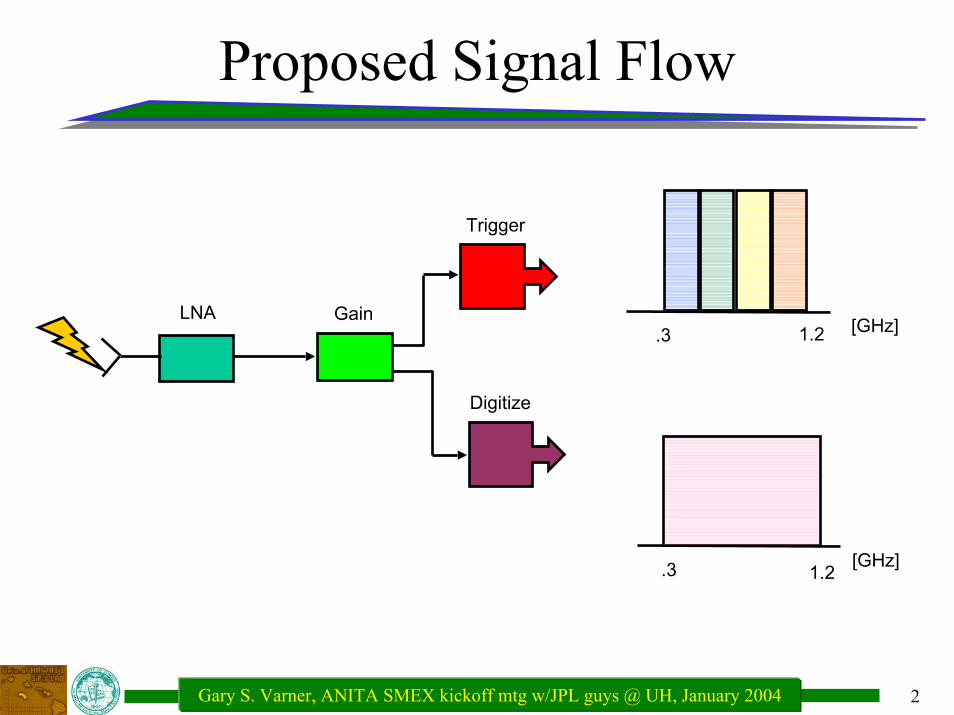
Proposed Signal Flow
LNA Gain
Digitize
Trigger
[GHz]1.2.3
[GHz].3 1.2
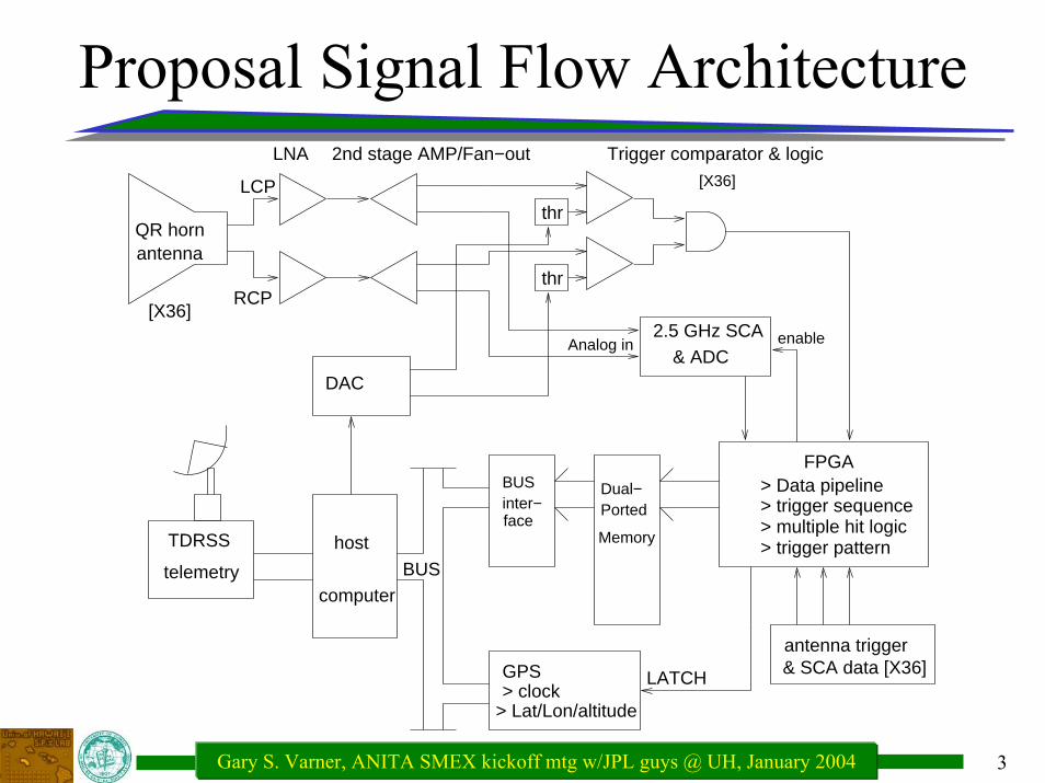
3Gary S. Varner, ANITA SMEX kickoff mtg w/JPL guys @ UH, January 2004
Proposal Signal Flow Architecture
BUSinter−
Dual−Ported
LATCH
LCP
RCP
FPGA
GPS> clock
> Lat/Lon/altitude
2nd stage AMP/Fan−out
faceMemory
Trigger comparator & logic
[X36]
> trigger sequence> multiple hit logic> trigger pattern
thr
thr
Analog in enable
[X36]
> Data pipeline
& SCA data [X36]
BUS
TDRSS
LNA
computer
host
telemetry
& ADC2.5 GHz SCA
antenna trigger
antennaQR horn
DAC
4Gary S. Varner, ANITA SMEX kickoff mtg w/JPL guys @ UH, January 2004
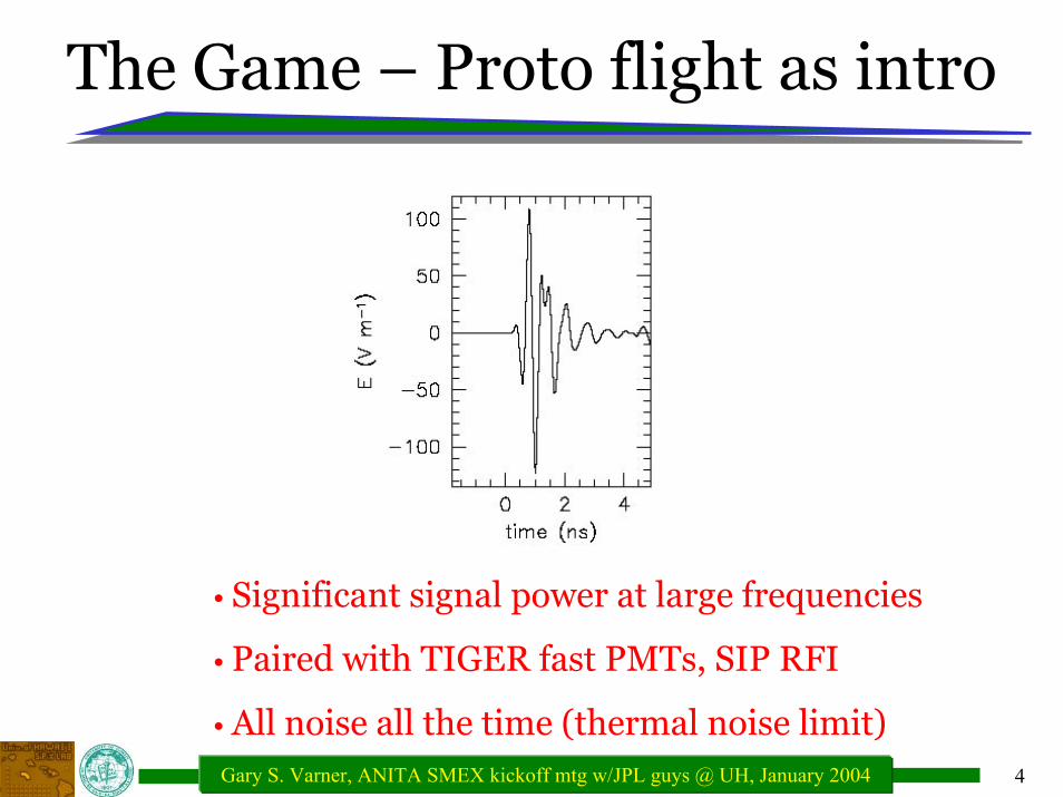
The Game – Proto flight as intro
• Significant signal power at large frequencies
• Paired with TIGER fast PMTs, SIP RFI
• All noise all the time (thermal noise limit)
5Gary S. Varner, ANITA SMEX kickoff mtg w/JPL guys @ UH, January 2004
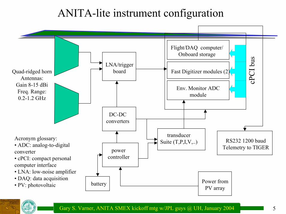
ANITA-lite instrument configuration
LNA/triggerboard
Flight/DAQ computer/ Onboard storage
transducerSuite (T,P,I,V,..)
Fast Digitizer modules (2)
Env. Monitor ADC module
powercontroller
DC-DCconverters
cPC
Ibus
Quad-ridged hornAntennas:
Gain 8-15 dBiFreq. Range:0.2-1.2 GHz
Power fromPV array
RS232 1200 baudTelemetry to TIGER
battery
Acronym glossary:• ADC: analog-to-digital converter• cPCI: compact personal computer interface• LNA: low-noise amplifier• DAQ: data acquisition• PV: photovoltaic
6Gary S. Varner, ANITA SMEX kickoff mtg w/JPL guys @ UH, January 2004
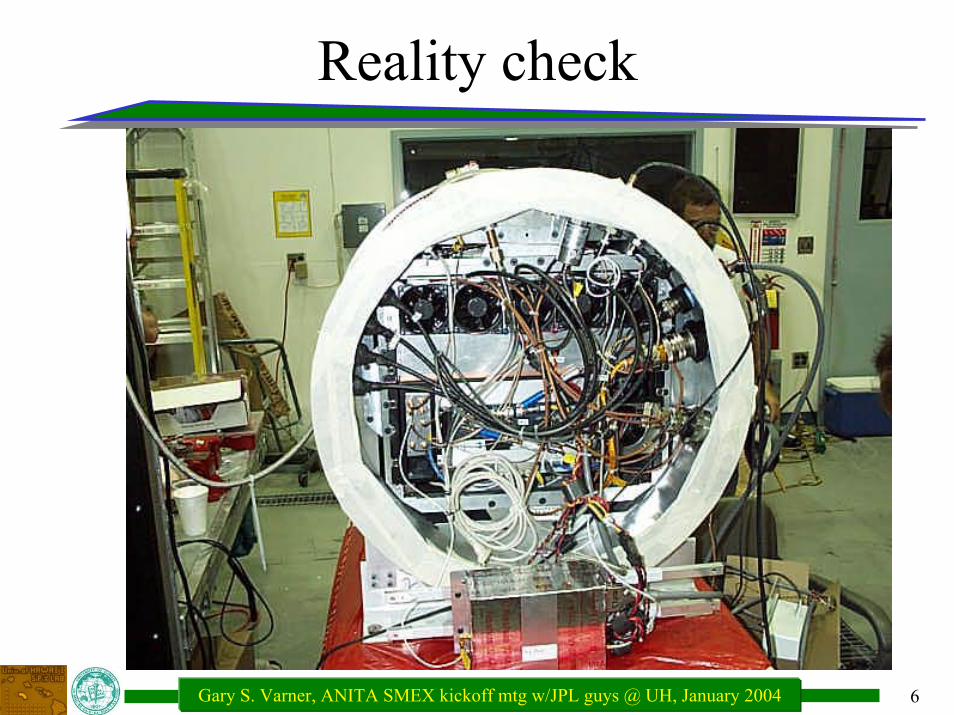
Reality check
7Gary S. Varner, ANITA SMEX kickoff mtg w/JPL guys @ UH, January 2004
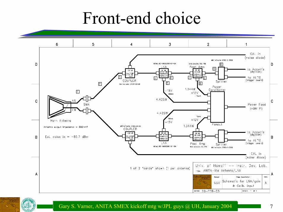
Front-end choice
8Gary S. Varner, ANITA SMEX kickoff mtg w/JPL guys @ UH, January 2004
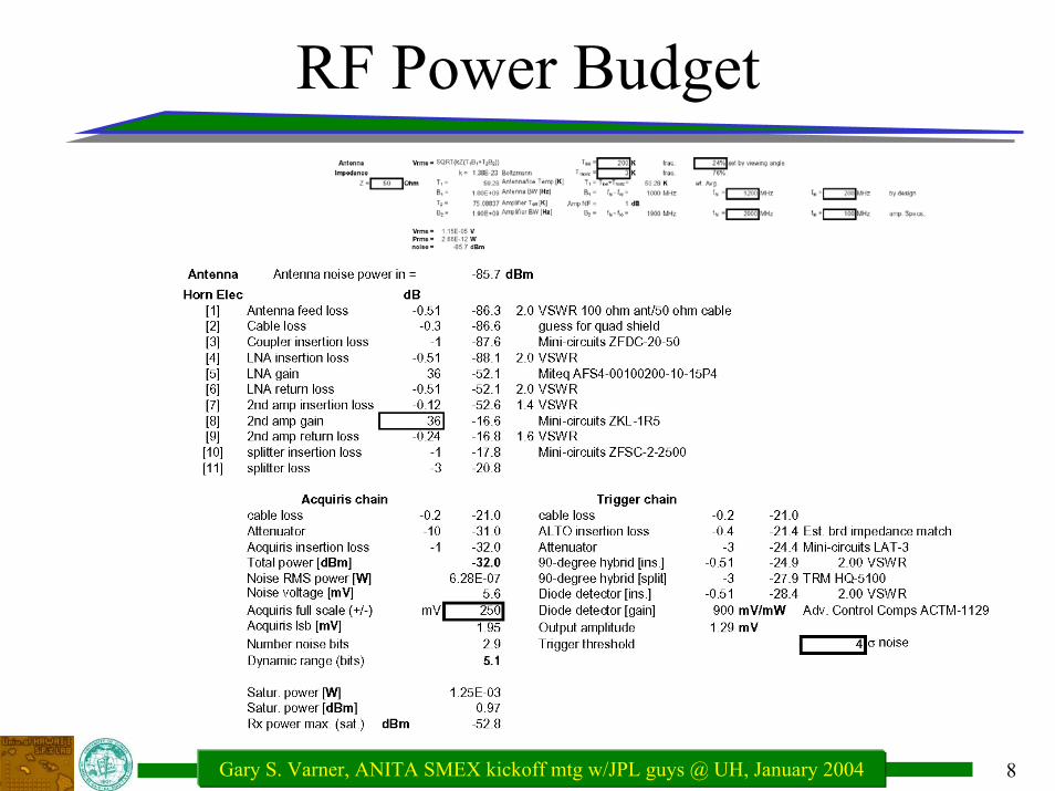
RF Power Budget
9Gary S. Varner, ANITA SMEX kickoff mtg w/JPL guys @ UH, January 2004
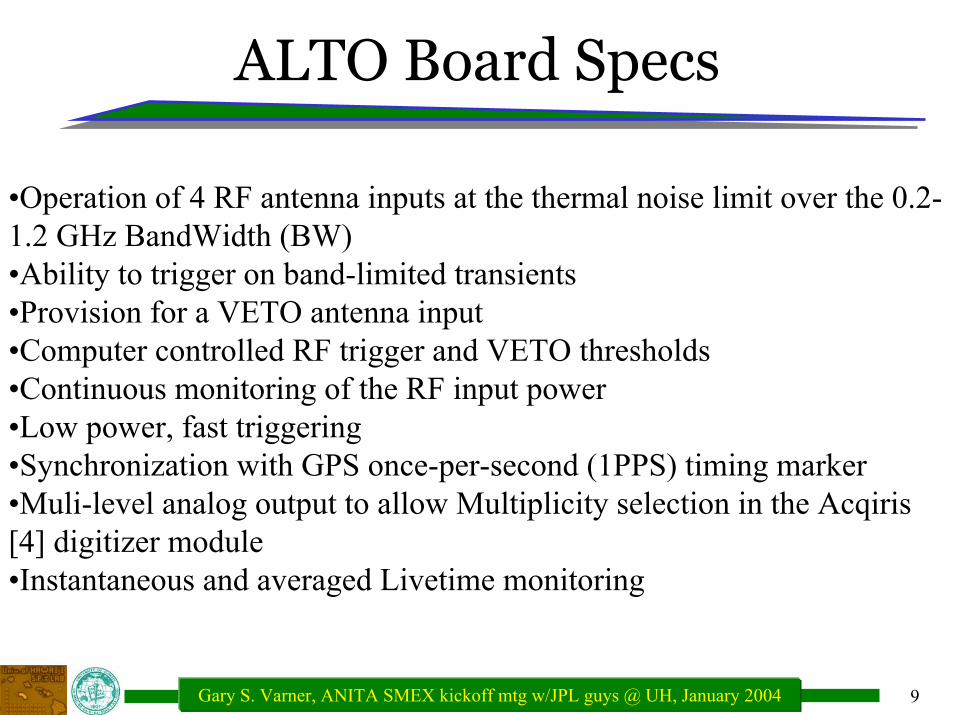
ALTO Board Specs
•Operation of 4 RF antenna inputs at the thermal noise limit over the 0.2-1.2 GHz BandWidth (BW) •Ability to trigger on band-limited transients•Provision for a VETO antenna input•Computer controlled RF trigger and VETO thresholds•Continuous monitoring of the RF input power•Low power, fast triggering•Synchronization with GPS once-per-second (1PPS) timing marker•Muli-level analog output to allow Multiplicity selection in the Acqiris [4] digitizer module•Instantaneous and averaged Livetime monitoring
10Gary S. Varner, ANITA SMEX kickoff mtg w/JPL guys @ UH, January 2004
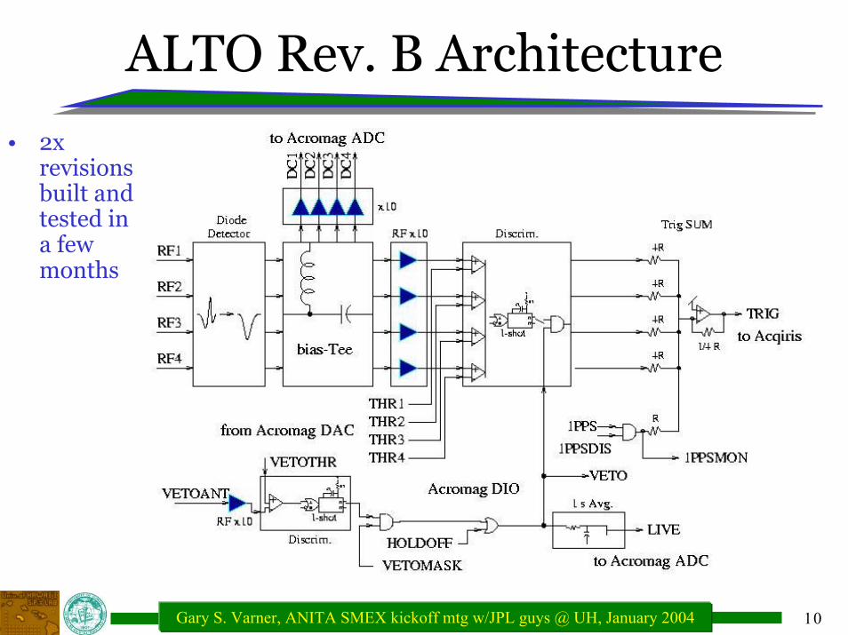
ALTO Rev. B Architecture
• 2x revisions built and tested in a few months
11Gary S. Varner, ANITA SMEX kickoff mtg w/JPL guys @ UH, January 2004
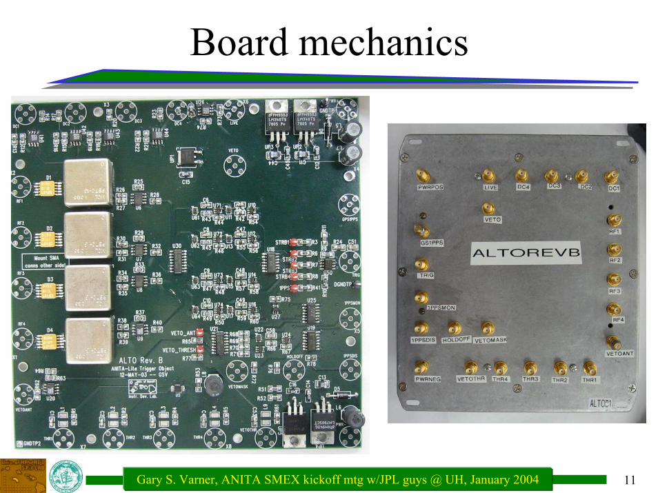
Board mechanics
12Gary S. Varner, ANITA SMEX kickoff mtg w/JPL guys @ UH, January 2004
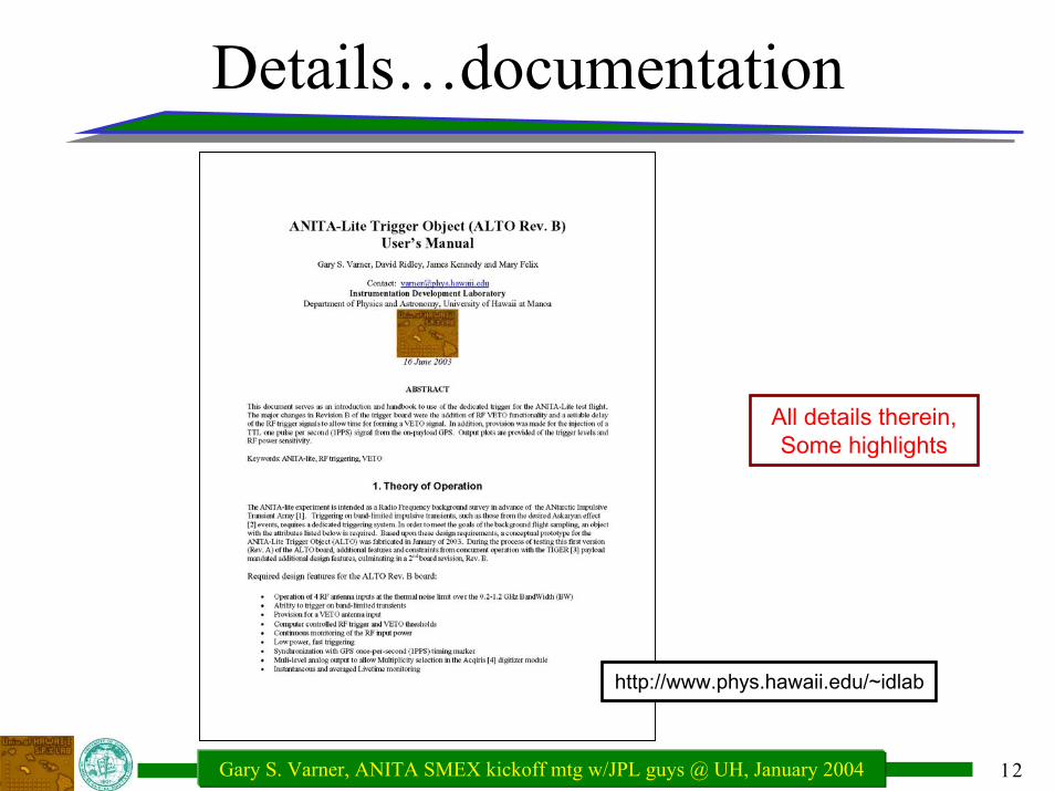
Details…documentation
http://www.phys.hawaii.edu/~idlab
All details therein,Some highlights
13Gary S. Varner, ANITA SMEX kickoff mtg w/JPL guys @ UH, January 2004
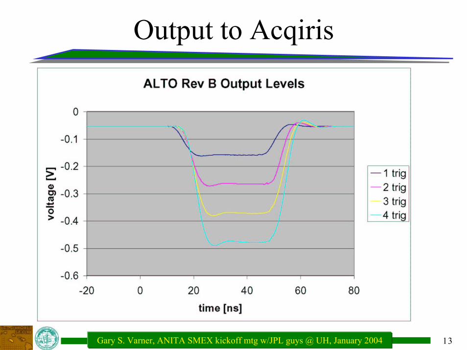
Output to Acqiris
14Gary S. Varner, ANITA SMEX kickoff mtg w/JPL guys @ UH, January 2004
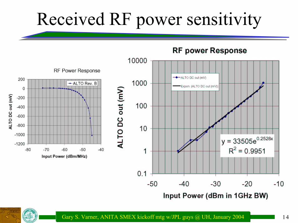
Received RF power sensitivity
15Gary S. Varner, ANITA SMEX kickoff mtg w/JPL guys @ UH, January 2004
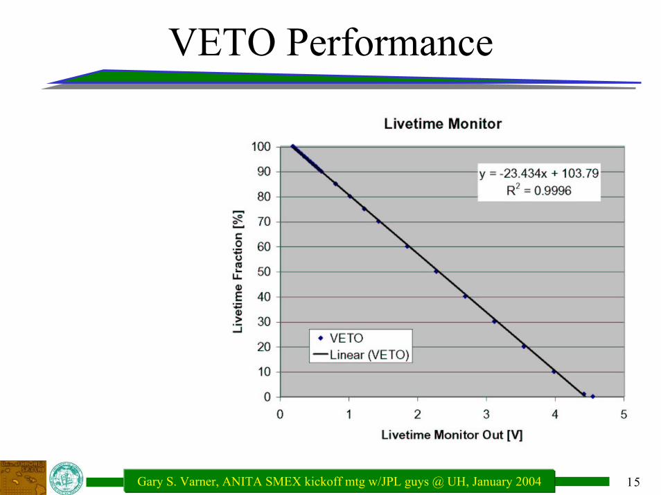
VETO Performance
16Gary S. Varner, ANITA SMEX kickoff mtg w/JPL guys @ UH, January 2004
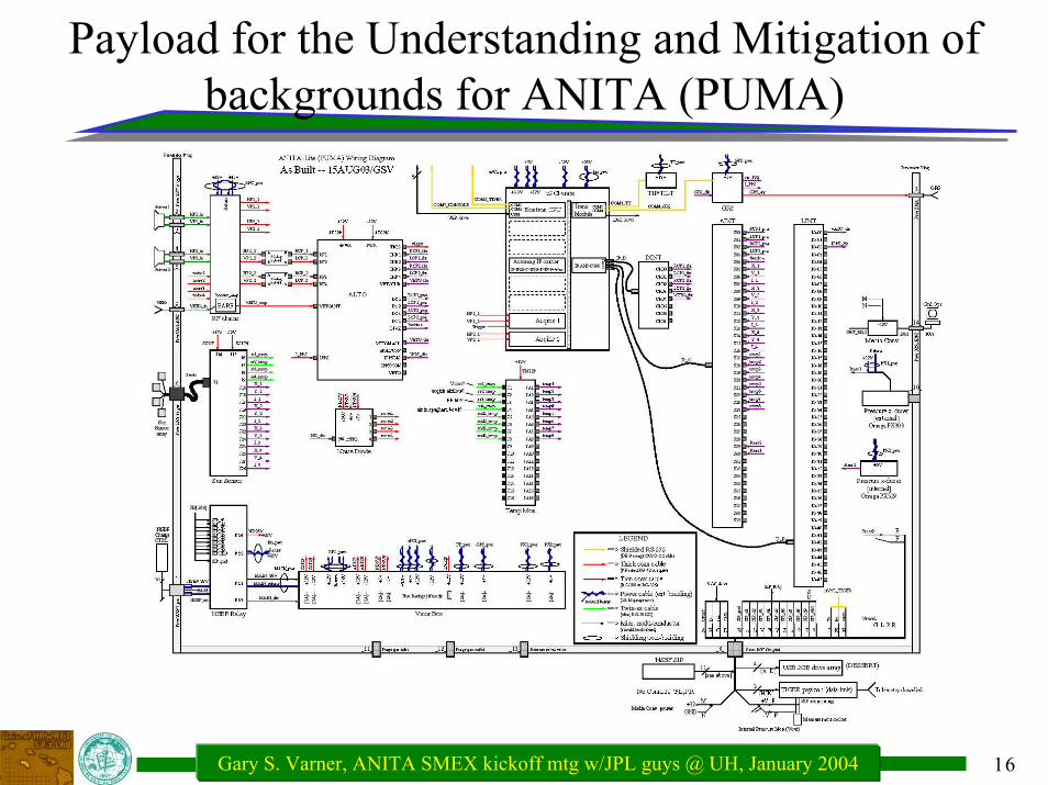
Payload for the Understanding and Mitigation of backgrounds for ANITA (PUMA)
17Gary S. Varner, ANITA SMEX kickoff mtg w/JPL guys @ UH, January 2004
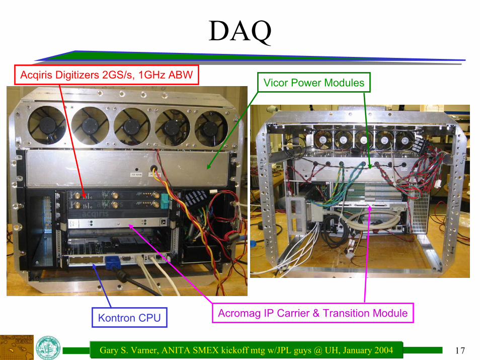
DAQAcqiris Digitizers 2GS/s, 1GHz ABW
Vicor Power Modules
Acromag IP Carrier & Transition ModuleKontron CPU
18Gary S. Varner, ANITA SMEX kickoff mtg w/JPL guys @ UH, January 2004
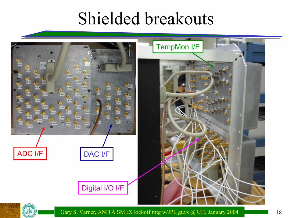
Shielded breakoutsTempMon I/F
ADC I/F DAC I/F
Digital I/O I/F
19Gary S. Varner, ANITA SMEX kickoff mtg w/JPL guys @ UH, January 2004
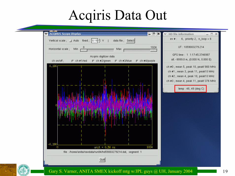
Acqiris Data Out
20Gary S. Varner, ANITA SMEX kickoff mtg w/JPL guys @ UH, January 2004
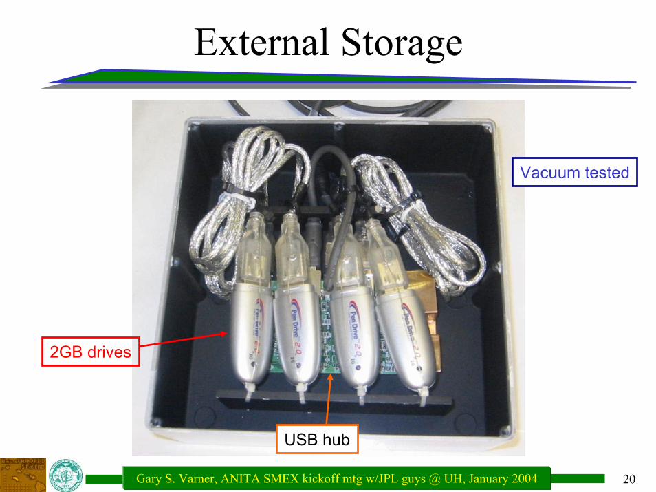
External Storage
USB hub
2GB drives
Vacuum tested
21Gary S. Varner, ANITA SMEX kickoff mtg w/JPL guys @ UH, January 2004
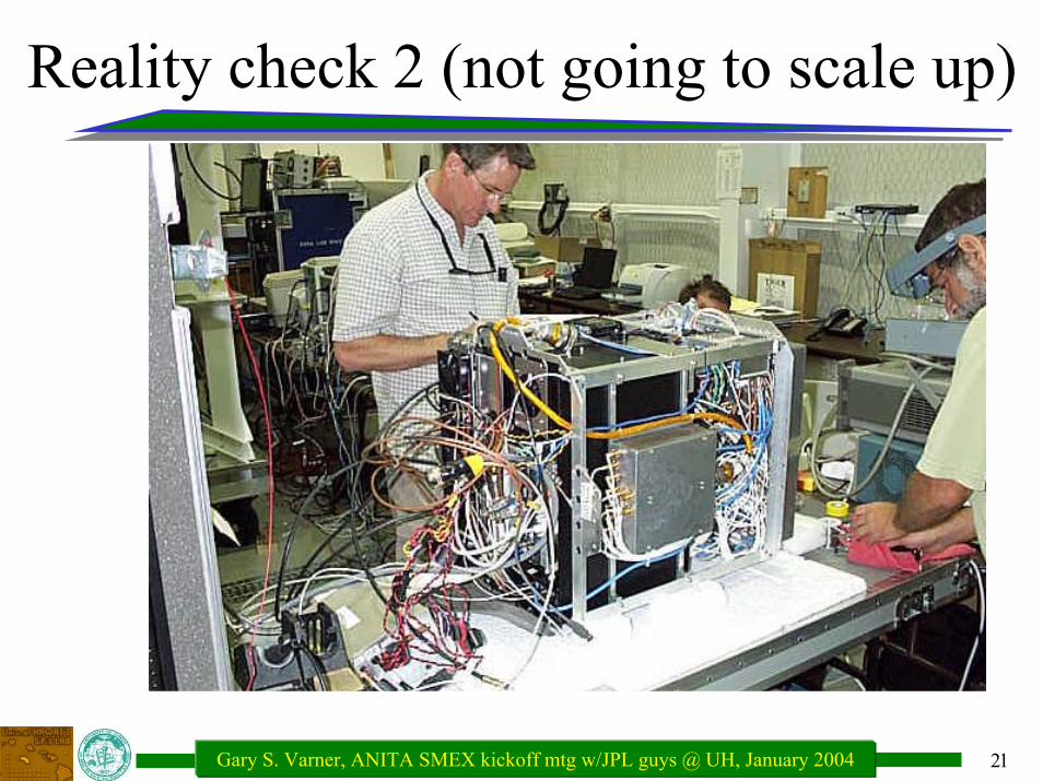
Reality check 2 (not going to scale up)
22Gary S. Varner, ANITA SMEX kickoff mtg w/JPL guys @ UH, January 2004
ANITA-lite Lessons (1)
• Mostly successful flight:– 1x ALTO channels went belly up– A lot of functionality not really implemented– Direct single channel rate monitoring (scalers) would help– Too many SMA cables
• Global Lessons:– Need better integration/packaging management– “RF front-end” part needs to be modular– Already at 200W for only 2 antennas, 2006 will come
quickly
• Major concern: Acqiris heating• Many items not covered
– Sun sensor, Noise diode, GPS
23Gary S. Varner, ANITA SMEX kickoff mtg w/JPL guys @ UH, January 2004
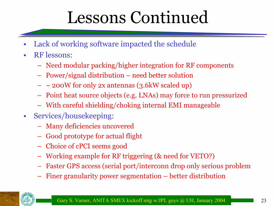
Lessons Continued• Lack of working software impacted the schedule
• RF lessons:– Need modular packing/higher integration for RF components
– Power/signal distribution – need better solution
– ~ 200W for only 2x antennas (3.6kW scaled up)
– Point heat source objects (e.g. LNAs) may force to run pressurized
– With careful shielding/choking internal EMI manageable
• Services/housekeeping:– Many deficiencies uncovered
– Good prototype for actual flight
– Choice of cPCI seems good
– Working example for RF triggering (& need for VETO?)
– Faster GPS access (serial port/interconn drop only serious problem
– Finer granularity power segmentation – better distribution

24Gary S. Varner, ANITA SMEX kickoff mtg w/JPL guys @ UH, January 2004
Askaryan Signature
0 2 4 6 8
Time (ns)
• Significant signal power at large frequencies
• Strong linear polarization (near 100%)
25Gary S. Varner, ANITA SMEX kickoff mtg w/JPL guys @ UH, January 2004
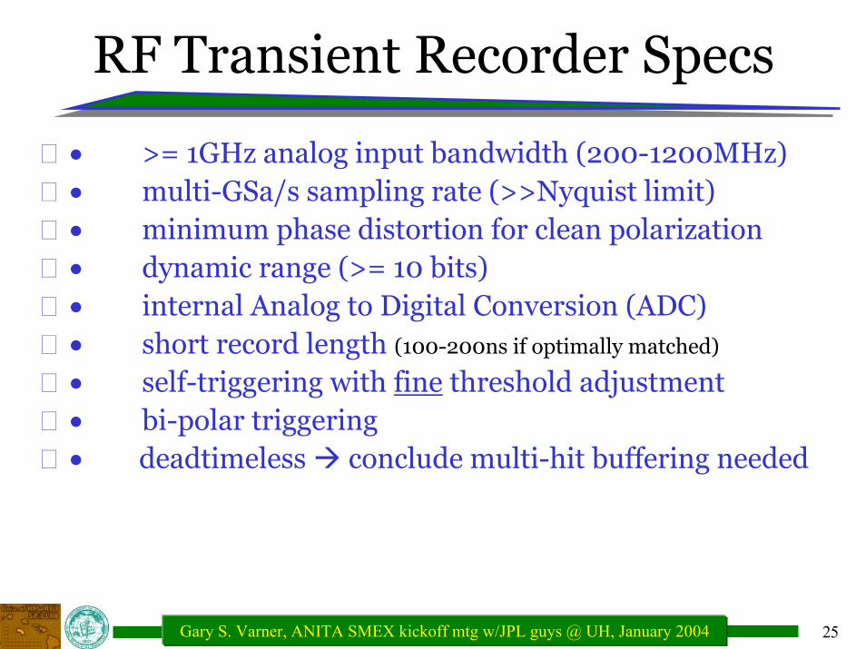
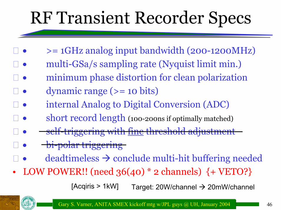
RF Transient Recorder Specs
• >= 1GHz analog input bandwidth (200-1200MHz)• multi-GSa/s sampling rate (>>Nyquist limit)• minimum phase distortion for clean polarization • dynamic range (>= 10 bits)• internal Analog to Digital Conversion (ADC)• short record length (100-200ns if optimally matched)
• self-triggering with fine threshold adjustment• bi-polar triggering• deadtimeless conclude multi-hit buffering needed
26Gary S. Varner, ANITA SMEX kickoff mtg w/JPL guys @ UH, January 2004
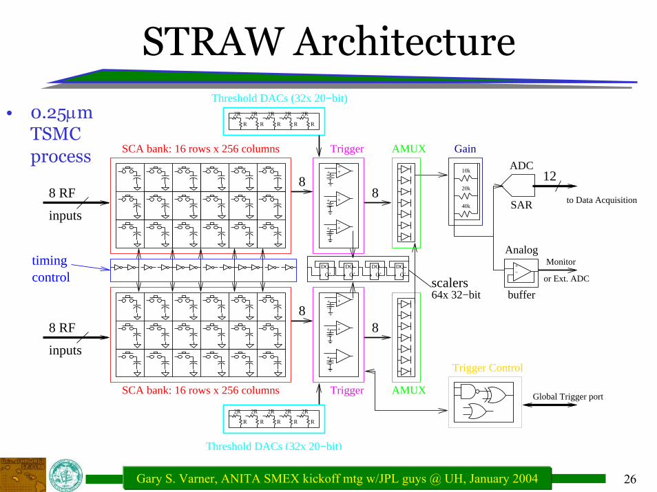
STRAW3 architectureSTRAW Architecture
40k
20k
10k
2R
R
2R
R
2R
RR
2R
R
2R
inputs
8 RF
inputs
8 RF
Analog
buffer
Trigger Control
AMUX
8
8
Monitor
or Ext. ADC
to Data Acquisition
Global Trigger port
Threshold DACs (32x 20−bit)
Threshold DACs (32x 20−bit)
64x 32−bit
12
timing control
SCA bank: 16 rows x 256 columns
SCA bank: 16 rows x 256 columns
8
8
Trigger
Trigger
AMUX
scalers
Gain
ADC
SAR
2R
R R
2R
R
2R
R
2R
R
2R
DQ
Q’
D Q
Q’
+−
Q
Q’
D Q
Q’
D
−+
+−
−+
−+
+−
+−
−+
+−
−+
+−
+−
−+
• 0.25µm TSMC process
27Gary S. Varner, ANITA SMEX kickoff mtg w/JPL guys @ UH, January 2004
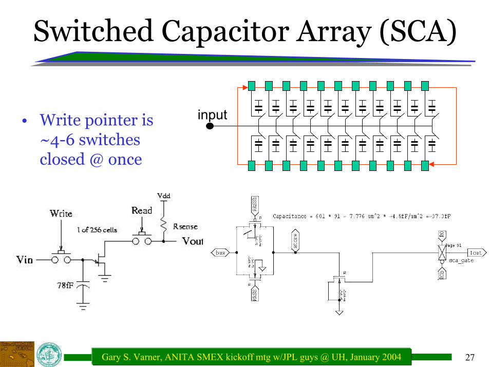
Switched Capacitor Array (SCA)
input• Write pointer is ~4-6 switches closed @ once
28Gary S. Varner, ANITA SMEX kickoff mtg w/JPL guys @ UH, January 2004
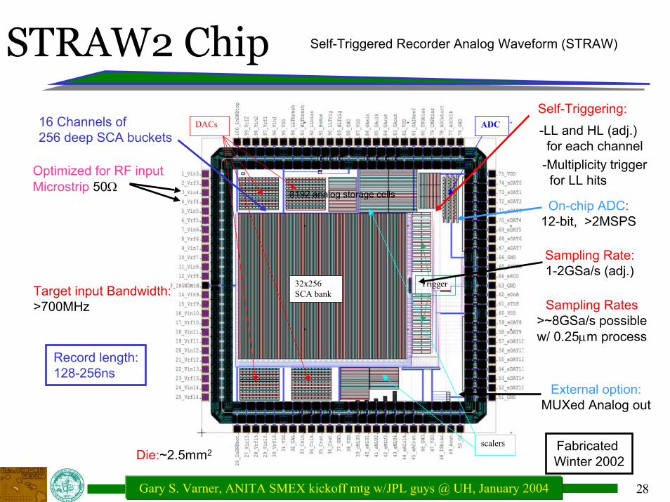
STRAW2 Chip Self-Triggered Recorder Analog Waveform (STRAW)
32x256 SCA bank
DACs ADC
Trigger
scalers
16 Channels of256 deep SCA buckets
Optimized for RF inputMicrostrip 50Ω
Record length:128-256ns
Target input Bandwidth:>700MHz
-LL and HL (adj.) for each channel
Sampling Rate:1-2GSa/s (adj.)
-Multiplicity triggerfor LL hits
On-chip ADC:12-bit, >2MSPS
External option:MUXed Analog out
Sampling Rates>~8GSa/s possiblew/ 0.25µm process
8192 analog storage cells
Die:~2.5mm2
Self-Triggering:
Fabricated Winter 2002
29Gary S. Varner, ANITA SMEX kickoff mtg w/JPL guys @ UH, January 2004
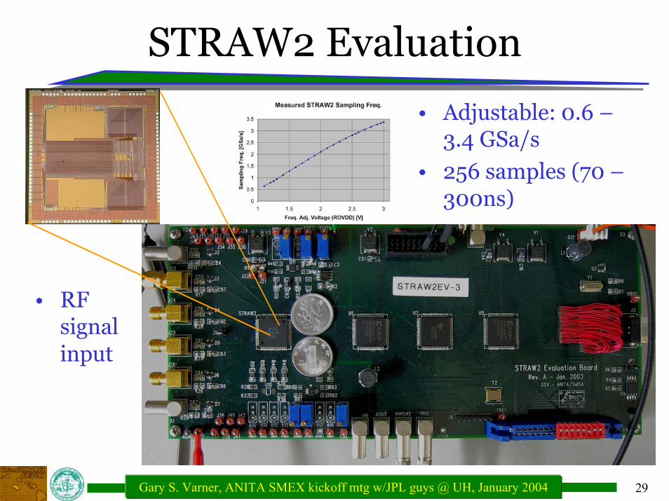
STRAW2 Evaluation
• RF signal input
• Adjustable: 0.6 –3.4 GSa/s
• 256 samples (70 –300ns)
30Gary S. Varner, ANITA SMEX kickoff mtg w/JPL guys @ UH, January 2004
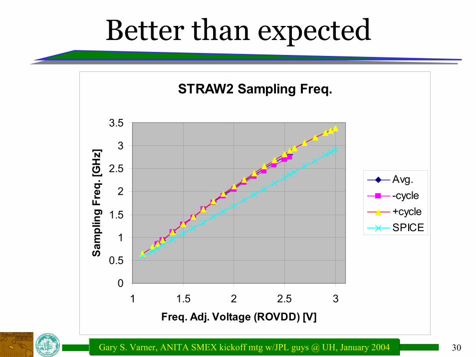
Better than expected
STRAW2 Sampling Freq.
0
0.5
1
1.5
2
2.5
3
3.5
1 1.5 2 2.5 3
Freq. Adj. Voltage (ROVDD) [V]
Sam
plin
g Fr
eq. [
GH
z]
Avg.-cycle+cycleSPICE
31Gary S. Varner, ANITA SMEX kickoff mtg w/JPL guys @ UH, January 2004
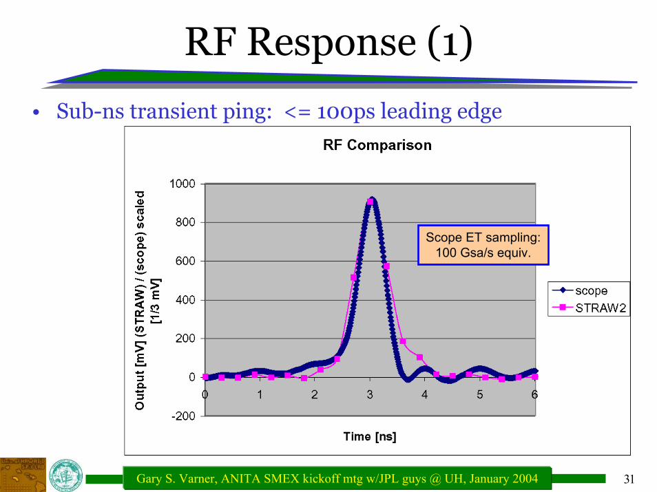
RF Response (1)
• Sub-ns transient ping: <= 100ps leading edge
Scope ET sampling:100 Gsa/s equiv.
32Gary S. Varner, ANITA SMEX kickoff mtg w/JPL guys @ UH, January 2004
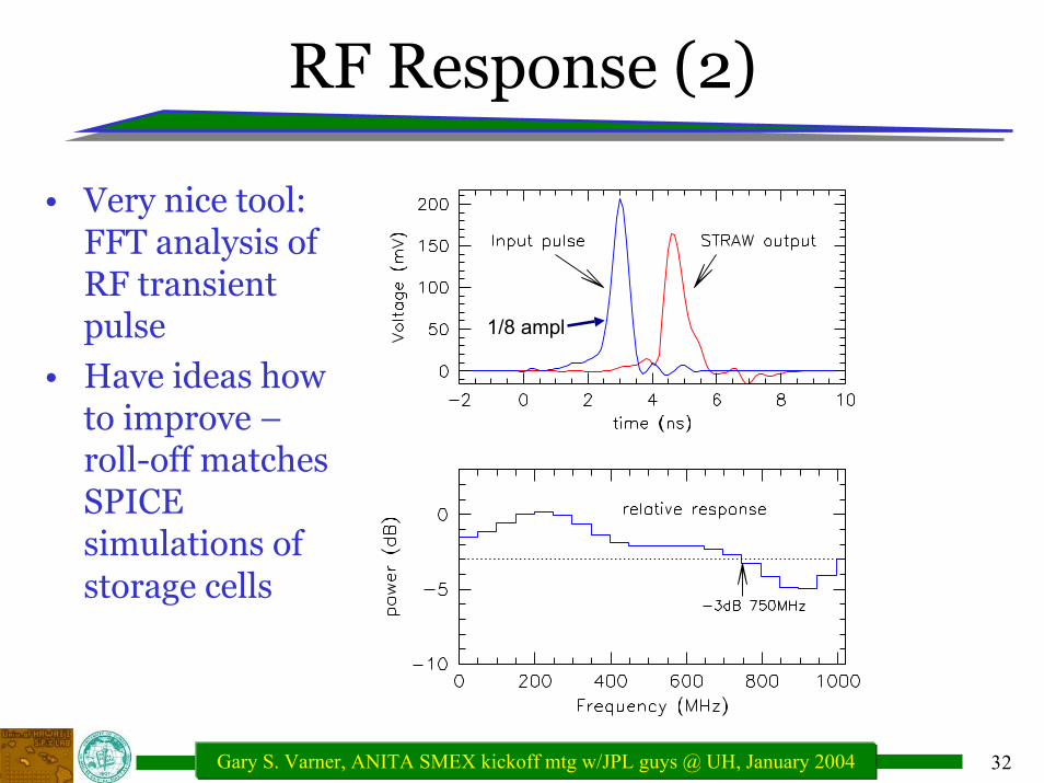
RF Response (2)
• Very nice tool: FFT analysis of RF transient pulse
• Have ideas how to improve –roll-off matches SPICE simulations of storage cells
1/8 ampl
33Gary S. Varner, ANITA SMEX kickoff mtg w/JPL guys @ UH, January 2004
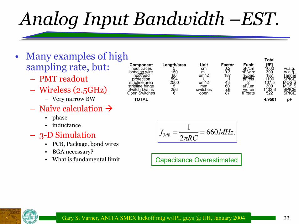
Analog Input Bandwidth –EST.
• Many examples of high sampling rate, but:– PMT readout– Wireless (2.5GHz)
– Very narrow BW
– Naïve calculation • phase• inductance
– 3-D Simulation• PCB, Package, bond wires• BGA necessary?• What is fundamental limit
Component Length/area Unit Factor FunitTotal [fF]
Input traces 5 cm 0.2 pF/cm 1000 w.a.g.bonding wire 150 mil 0.3 pF/wire 300 w.a.g.
input pad 60 um^2 187 fF/pad 187 Tannerinput protection 594 λ 1.1 pF/ckt 1100 SPICE
stripline area 2500 um^2 43aF/um^
2 107.5 MOSISstripline fringe 5 mm 60 aF/um 300 MOSISSwitch Drains 256 switches 5.6 fF/drain 1433.6 SPICE
Open Switches 6 open 87 fF/gate 522 SPICETOTAL 4.9501 pF
.6602
13 MHz
RCf dB ==
π
Capacitance Overestimated
34Gary S. Varner, ANITA SMEX kickoff mtg w/JPL guys @ UH, January 2004
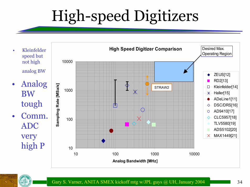
High-speed Digitizers
• Kleinfelder speed but not high
analog BW
High Speed Digitizer Comparison
10
100
1000
10000
10 100 1000 10000
Analog Bandwidth [MHz]
Sam
plin
g R
ate
[MS
a/s]
ZEUS[12]RD2[13]Kleinfelder[14]Haller[15]ADeLine1[11]DSC/DRS[16]AD9410[17]CLC5957[18]TLV5580[19]ADS5102[20]MAX1449[21]
Desired Max.Operating Region
STRAW2• Analog BW tough
• Comm. ADC very high P
35Gary S. Varner, ANITA SMEX kickoff mtg w/JPL guys @ UH, January 2004
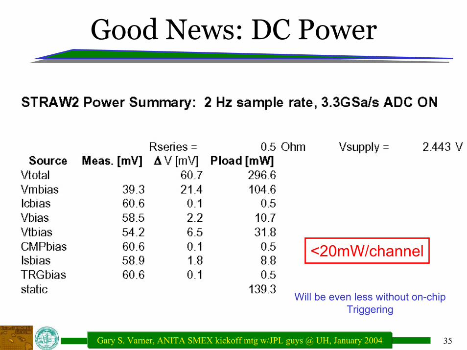
Good News: DC Power
<20mW/channel
Will be even less without on-chipTriggering
36Gary S. Varner, ANITA SMEX kickoff mtg w/JPL guys @ UH, January 2004
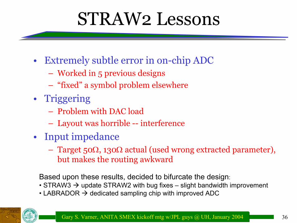
STRAW2 Lessons
• Extremely subtle error in on-chip ADC– Worked in 5 previous designs
– “fixed” a symbol problem elsewhere
• Triggering– Problem with DAC load
– Layout was horrible -- interference
• Input impedance– Target 50Ω, 130Ω actual (used wrong extracted parameter),
but makes the routing awkward
Based upon these results, decided to bifurcate the design:• STRAW3 update STRAW2 with bug fixes – slight bandwidth improvement• LABRADOR dedicated sampling chip with improved ADC
37Gary S. Varner, ANITA SMEX kickoff mtg w/JPL guys @ UH, January 2004
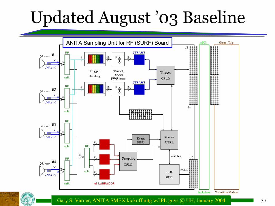
Updated August ’03 Baseline ANITA Sampling Unit for RF (SURF) Board
38Gary S. Varner, ANITA SMEX kickoff mtg w/JPL guys @ UH, January 2004
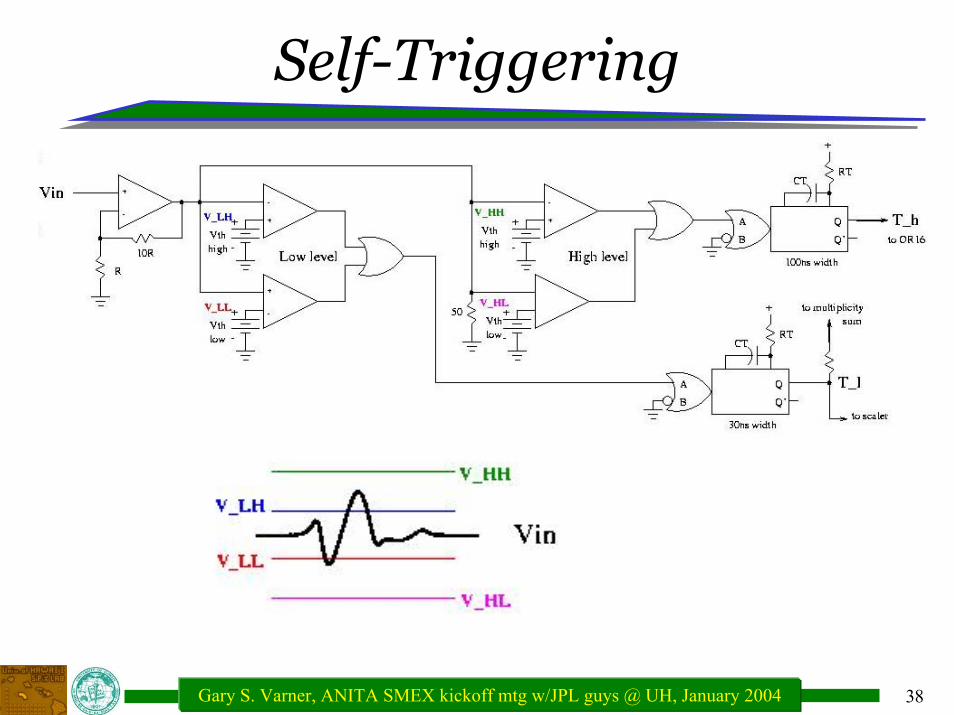
Self-Triggering
39Gary S. Varner, ANITA SMEX kickoff mtg w/JPL guys @ UH, January 2004
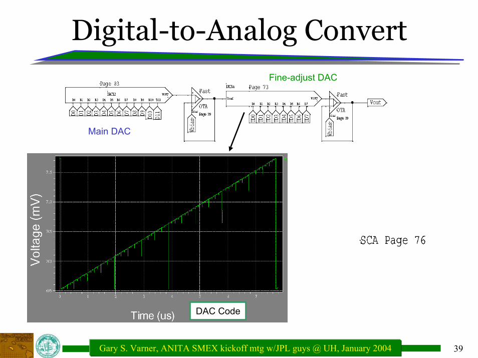
Digital-to-Analog Convert
Main DAC
Fine-adjust DAC
DAC Code
40Gary S. Varner, ANITA SMEX kickoff mtg w/JPL guys @ UH, January 2004
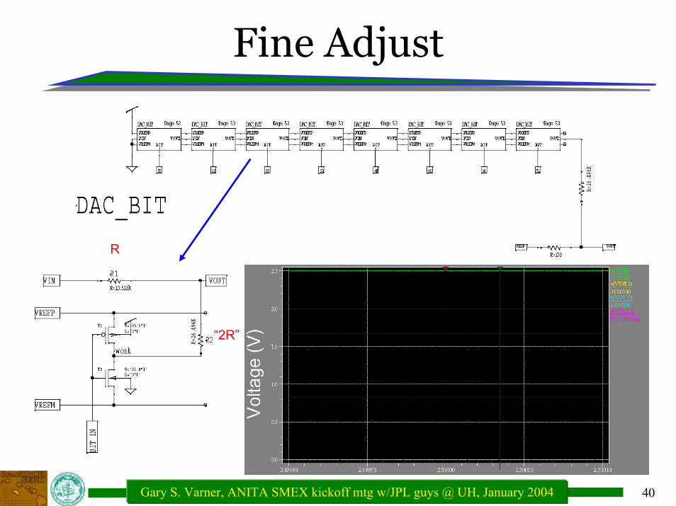
Fine Adjust
R
“2R”
41Gary S. Varner, ANITA SMEX kickoff mtg w/JPL guys @ UH, January 2004
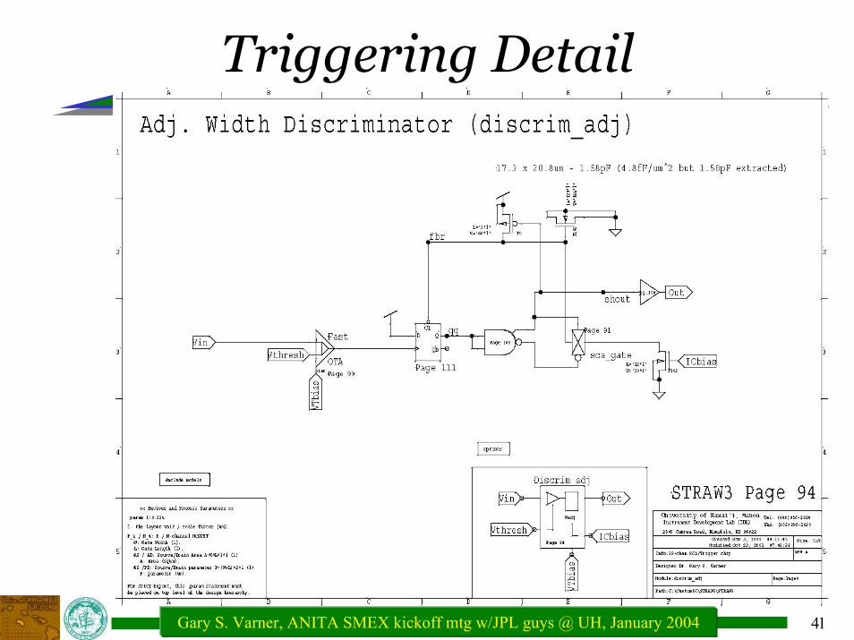
Triggering Detail
42Gary S. Varner, ANITA SMEX kickoff mtg w/JPL guys @ UH, January 2004
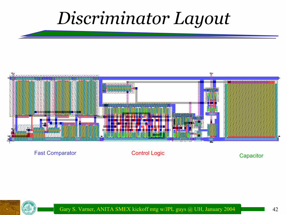
Discriminator Layout
Fast Comparator Control Logic Capacitor
43Gary S. Varner, ANITA SMEX kickoff mtg w/JPL guys @ UH, January 2004
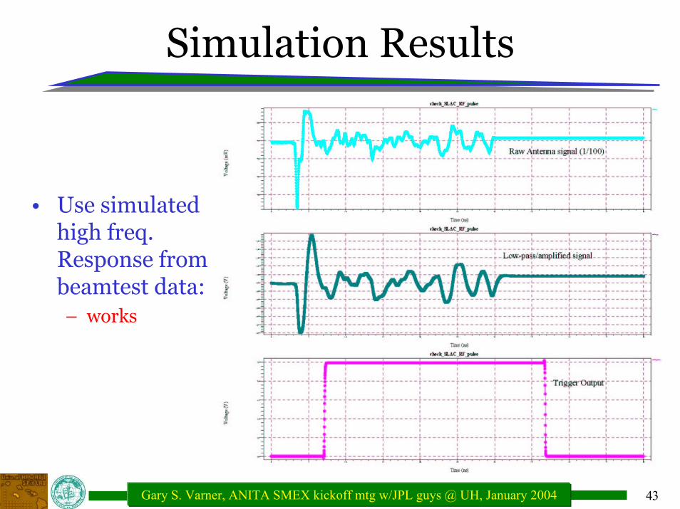
Simulation Results
• Use simulated high freq. Response from beamtest data:– works
44Gary S. Varner, ANITA SMEX kickoff mtg w/JPL guys @ UH, January 2004
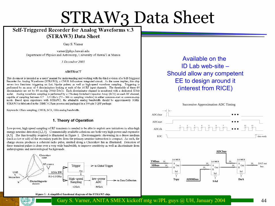
STRAW3 Data Sheet
16
16
16
SDbusTMbus
ADCbus
2:1 MUX
Out
Sel
B
A
TspySAd
ADDRbus DnA
busDAT out
16
2:1 MUX
Out
Sel
B
A16
1616
2:1 MUX
Out
Sel
B
A
data ready
12
Successive Approximation ADC Timing
1376543
EOC
ADCclear
ADCstart
ADCclk
1 2
Available on the ID Lab web-site –
Should allow any competentEE to design around it(interest from RICE)
45Gary S. Varner, ANITA SMEX kickoff mtg w/JPL guys @ UH, January 2004
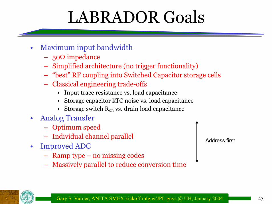
LABRADOR Goals
• Maximum input bandwidth– 50Ω impedance– Simplified architecture (no trigger functionality)– “best” RF coupling into Switched Capacitor storage cells– Classical engineering trade-offs
• Input trace resistance vs. load capacitance• Storage capacitor kTC noise vs. load capacitance• Storage switch Ron vs. drain load capacitance
• Analog Transfer– Optimum speed– Individual channel parallel
• Improved ADC– Ramp type – no missing codes– Massively parallel to reduce conversion time
Address first
46Gary S. Varner, ANITA SMEX kickoff mtg w/JPL guys @ UH, January 2004
RF Transient Recorder Specs
• >= 1GHz analog input bandwidth (200-1200MHz)
• multi-GSa/s sampling rate (Nyquist limit min.)
• minimum phase distortion for clean polarization
• dynamic range (>= 10 bits)
• internal Analog to Digital Conversion (ADC)
• short record length (100-200ns if optimally matched)
• self-triggering with fine threshold adjustment
• bi-polar triggering
• deadtimeless conclude multi-hit buffering needed
• LOW POWER!! (need 36(40) * 2 channels) + VETO?
[Acqiris > 1kW] Target: 20W/channel 20mW/channel
47Gary S. Varner, ANITA SMEX kickoff mtg w/JPL guys @ UH, January 2004
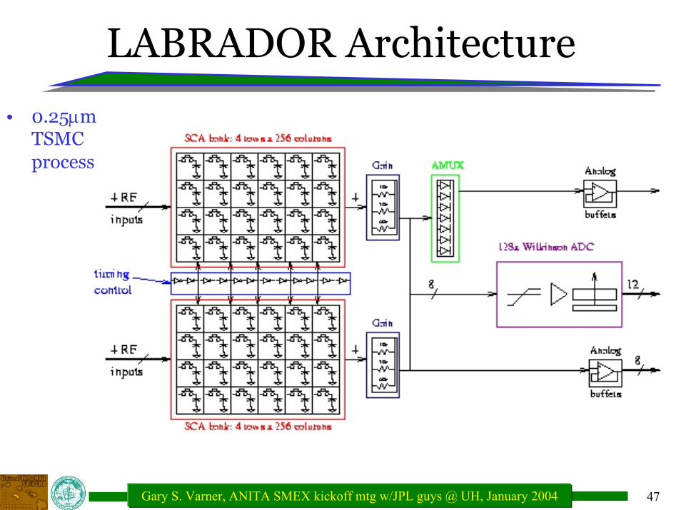
LABRADOR Architecture
• 0.25µm TSMC process
48Gary S. Varner, ANITA SMEX kickoff mtg w/JPL guys @ UH, January 2004
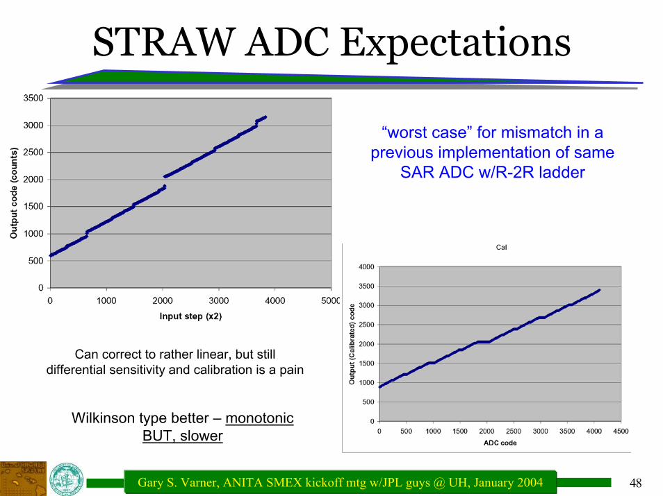
STRAW ADC Expectations
“worst case” for mismatch in a previous implementation of same
SAR ADC w/R-2R ladder
Can correct to rather linear, but still differential sensitivity and calibration is a pain
Wilkinson type better – monotonicBUT, slower
49Gary S. Varner, ANITA SMEX kickoff mtg w/JPL guys @ UH, January 2004
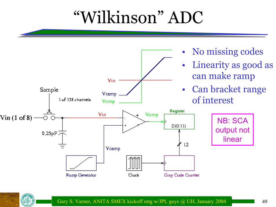
“Wilkinson” ADC
+-
• No missing codes
• Linearity as good as can make ramp
• Can bracket range of interest
NB: SCA output not
linear
50Gary S. Varner, ANITA SMEX kickoff mtg w/JPL guys @ UH, January 2004
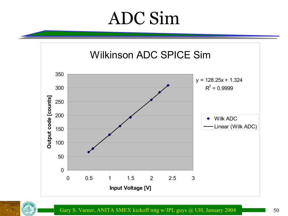
ADC Sim
Wilkinson ADC SPICE Sim
y = 128.25x + 1.324R2 = 0.9999
0
50
100
150
200
250
300
350
0 0.5 1 1.5 2 2.5 3
Input Voltage [V]
Out
put c
ode
[cou
nts]
Wilk ADCLinear (Wilk ADC)
51Gary S. Varner, ANITA SMEX kickoff mtg w/JPL guys @ UH, January 2004
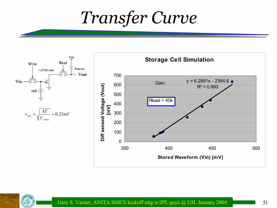
Transfer Curve
Storage Cell Simulation
y = 6.2891x - 2364.8R2 = 0.993
0
100
200
300
400
500
600
700
350 400 450 500
Stored Waveform (Vin) [mV]
Diff
sen
sed
Volta
ge (V
out)
[mV]
Rload = 40k
Gain:
mVCkTvstore
rms 23.0==
52Gary S. Varner, ANITA SMEX kickoff mtg w/JPL guys @ UH, January 2004
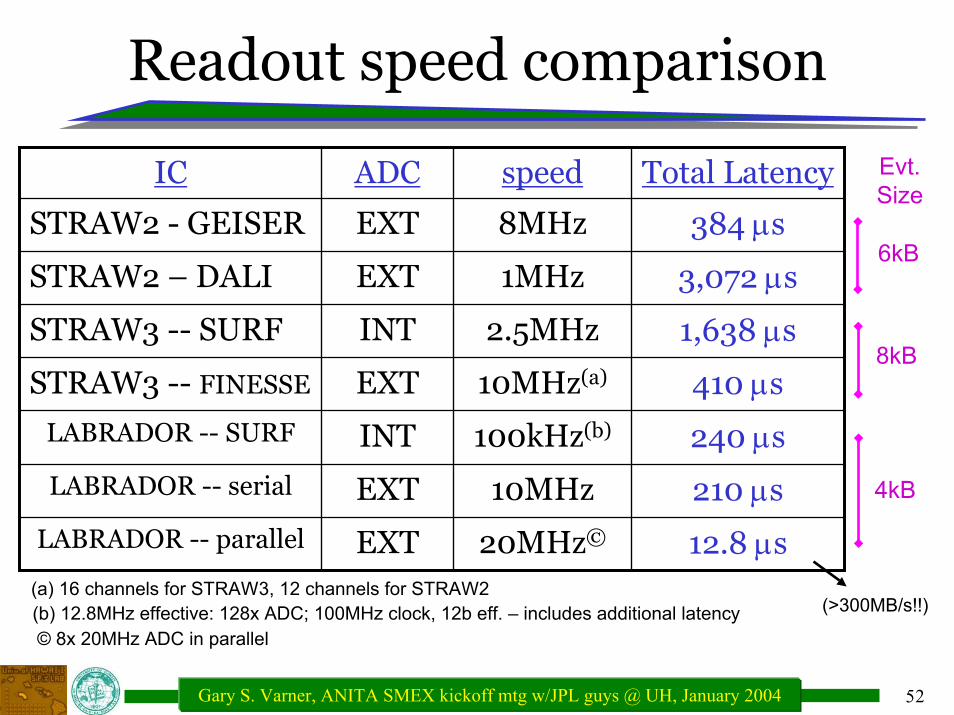
Readout speed comparison
12.8 µs20MHz©EXTLABRADOR -- parallel
210 µs10MHzEXTLABRADOR -- serial
240 µs100kHz(b)INTLABRADOR -- SURF
410 µs10MHz(a)EXTSTRAW3 -- FINESSE
1,638 µs2.5MHzINTSTRAW3 -- SURF
3,072 µs1MHzEXTSTRAW2 – DALI
384 µs8MHzEXTSTRAW2 - GEISER
Total LatencyspeedADCIC Evt.Size
6kB
8kB
4kB
(a) 16 channels for STRAW3, 12 channels for STRAW2(>300MB/s!!)(b) 12.8MHz effective: 128x ADC; 100MHz clock, 12b eff. – includes additional latency
© 8x 20MHz ADC in parallel
53Gary S. Varner, ANITA SMEX kickoff mtg w/JPL guys @ UH, January 2004
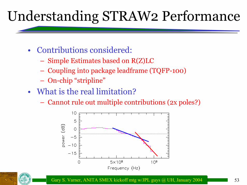
Understanding STRAW2 Performance
• Contributions considered:– Simple Estimates based on R(Z)LC
– Coupling into package leadframe (TQFP-100)
– On-chip “stripline”
• What is the real limitation?– Cannot rule out multiple contributions (2x poles?)
54Gary S. Varner, ANITA SMEX kickoff mtg w/JPL guys @ UH, January 2004
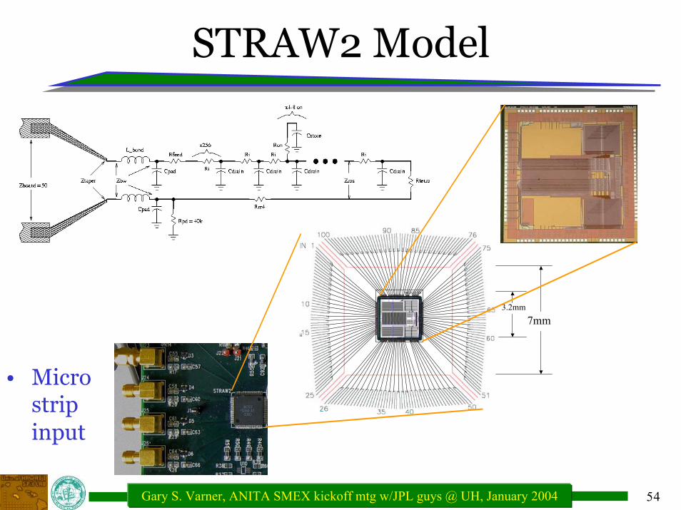
STRAW2 Model
7mm3.2mm
MOSIS ID
ii
• Microstripinput
55Gary S. Varner, ANITA SMEX kickoff mtg w/JPL guys @ UH, January 2004
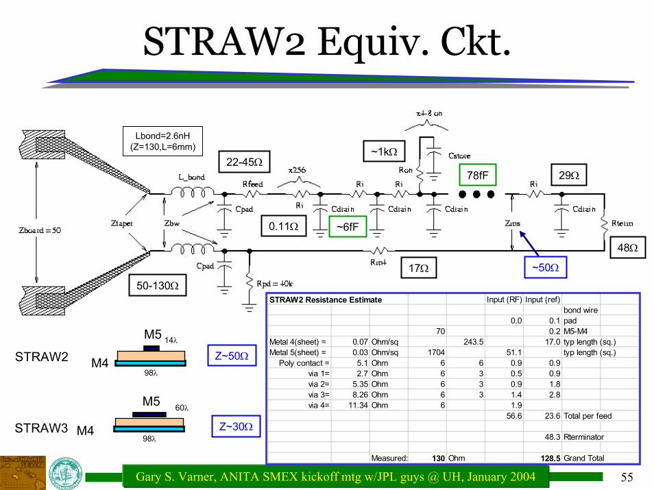
STRAW2 Equiv. Ckt.
STRAW2 Resistance Estimate Input (RF) Input (ref)bond wire
0.0 0.1 pad70 0.2 M5-M4
Metal 4(sheet) = 0.07 Ohm/sq 243.5 17.0 typ length (sq.)Metal 5(sheet) = 0.03 Ohm/sq 1704 51.1 typ length (sq.)
Poly contact = 5.1 Ohm 6 6 0.9 0.9via 1= 2.7 Ohm 6 3 0.5 0.9via 2= 5.35 Ohm 6 3 0.9 1.8via 3= 8.26 Ohm 6 3 1.4 2.8via 4= 11.34 Ohm 6 1.9
56.6 23.6 Total per feed
48.3 Rterminator
Measured: 130 Ohm 128.5 Grand Total
17Ω
29Ω
48Ω
~50Ω
78fF
~1kΩ
~6fF0.11Ω
22-45Ω
50-130Ω
M5 14λ
Lbond=2.6nH(Z=130,L=6mm)
STRAW2 Z~50ΩM498λ
M5 60λ
Z~30ΩSTRAW3 M498λ
56Gary S. Varner, ANITA SMEX kickoff mtg w/JPL guys @ UH, January 2004
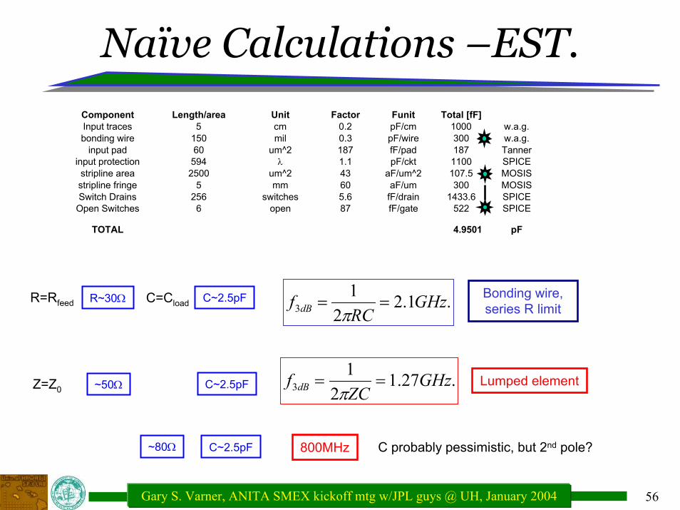
Naïve Calculations –EST.
Component Length/area Unit Factor Funit Total [fF]Input traces 5 cm 0.2 pF/cm 1000 w.a.g.bonding wire 150 mil 0.3 pF/wire 300 w.a.g.
input pad 60 um^2 187 fF/pad 187 Tannerinput protection 594 λ 1.1 pF/ckt 1100 SPICEstripline area 2500 um^2 43 aF/um^2 107.5 MOSISstripline fringe 5 mm 60 aF/um 300 MOSISSwitch Drains 256 switches 5.6 fF/drain 1433.6 SPICE
Open Switches 6 open 87 fF/gate 522 SPICE
TOTAL 4.9501 pF
.1.22
13 GHz
RCf dB ==
πBonding wire, series R limit
R=Rfeed C=Cload C~2.5pFR~30Ω
.27.12
13 GHz
ZCf dB ==
πLumped elementZ=Z0 C~2.5pF~50Ω
C probably pessimistic, but 2nd pole?800MHz~80Ω C~2.5pF
57Gary S. Varner, ANITA SMEX kickoff mtg w/JPL guys @ UH, January 2004
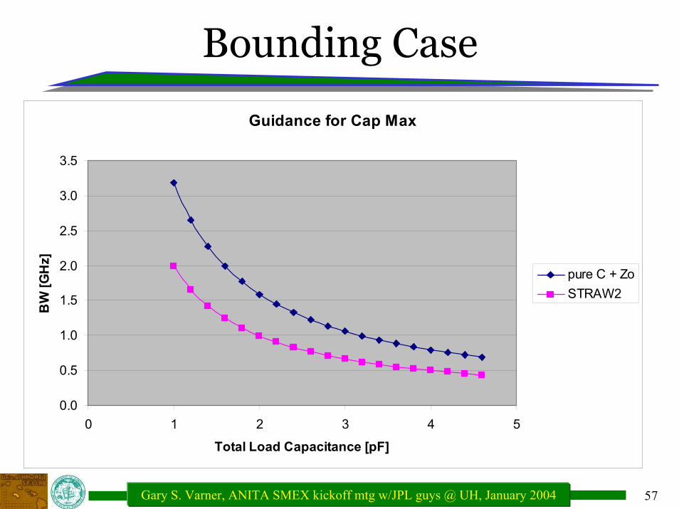
Bounding Case
Guidance for Cap Max
0.0
0.5
1.0
1.5
2.0
2.5
3.0
3.5
0 1 2 3 4 5
Total Load Capacitance [pF]
BW
[GH
z]
pure C + ZoSTRAW2
58Gary S. Varner, ANITA SMEX kickoff mtg w/JPL guys @ UH, January 2004
Storage Capacitor constraints
Impact of Storage Cap size
0
0.5
1
1.5
2
2.5
0 50 100 150 200
Storage Cap [fF]
Vrm
s [
mV
]
Vrms
STRAW2
For 1V useable input range
9bits
10bits
11bits
12bits
mVCkTvstore
rms 23.0==
Cstore only 78fF !!
Too big??
DC SPICE sim shows can make Rstatic ~ 920Ω, but there is a dynamic component also.
59Gary S. Varner, ANITA SMEX kickoff mtg w/JPL guys @ UH, January 2004
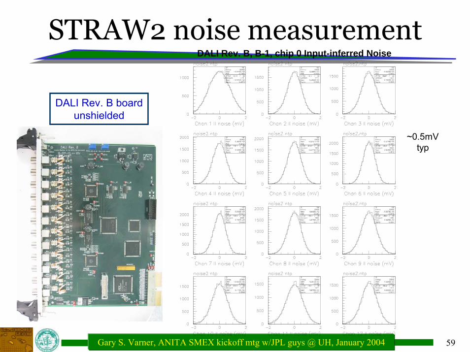
STRAW2 noise measurementDALI Rev. B, B-1, chip 0 Input-inferred Noise
DALI Rev. B boardunshielded
~0.5mVtyp
60Gary S. Varner, ANITA SMEX kickoff mtg w/JPL guys @ UH, January 2004
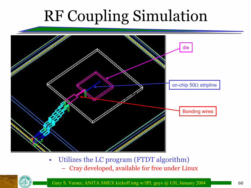
RF Coupling Simulation
.4.62
13 GHz
RCf dB ==
π.4.6
21
3 GHzRC
f dB ==π
.4.62
13 GHz
RCf dB ==
π.4.6
21
3 GHzRC
f dB ==π
die
on-chip 50Ω stripline
Bonding wires
• Utilizes the LC program (FTDT algorithm)– Cray developed, available for free under Linux
61Gary S. Varner, ANITA SMEX kickoff mtg w/JPL guys @ UH, January 2004
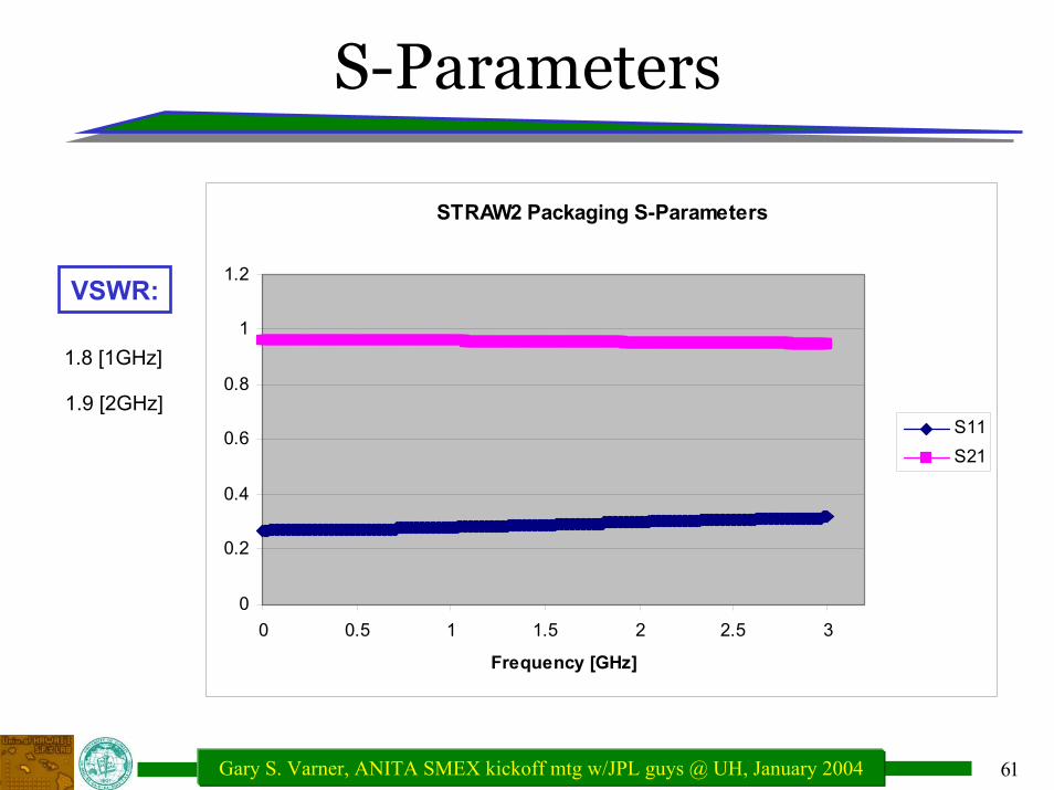
S-Parameters
STRAW2 Packaging S-Parameters
0
0.2
0.4
0.6
0.8
1
1.2
0 0.5 1 1.5 2 2.5 3
Frequency [GHz]
S11S21
VSWR:
1.8 [1GHz]
1.9 [2GHz]
62Gary S. Varner, ANITA SMEX kickoff mtg w/JPL guys @ UH, January 2004
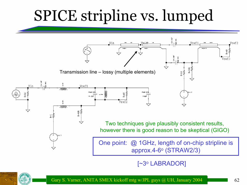
SPICE stripline vs. lumped
Transmission line – lossy (multiple elements)
Two techniques give plausibly consistent results, however there is good reason to be skeptical (GIGO)
One point: @ 1GHz, length of on-chip stripline is approx.4-6o (STRAW2/3)
[~3o LABRADOR]
63Gary S. Varner, ANITA SMEX kickoff mtg w/JPL guys @ UH, January 2004
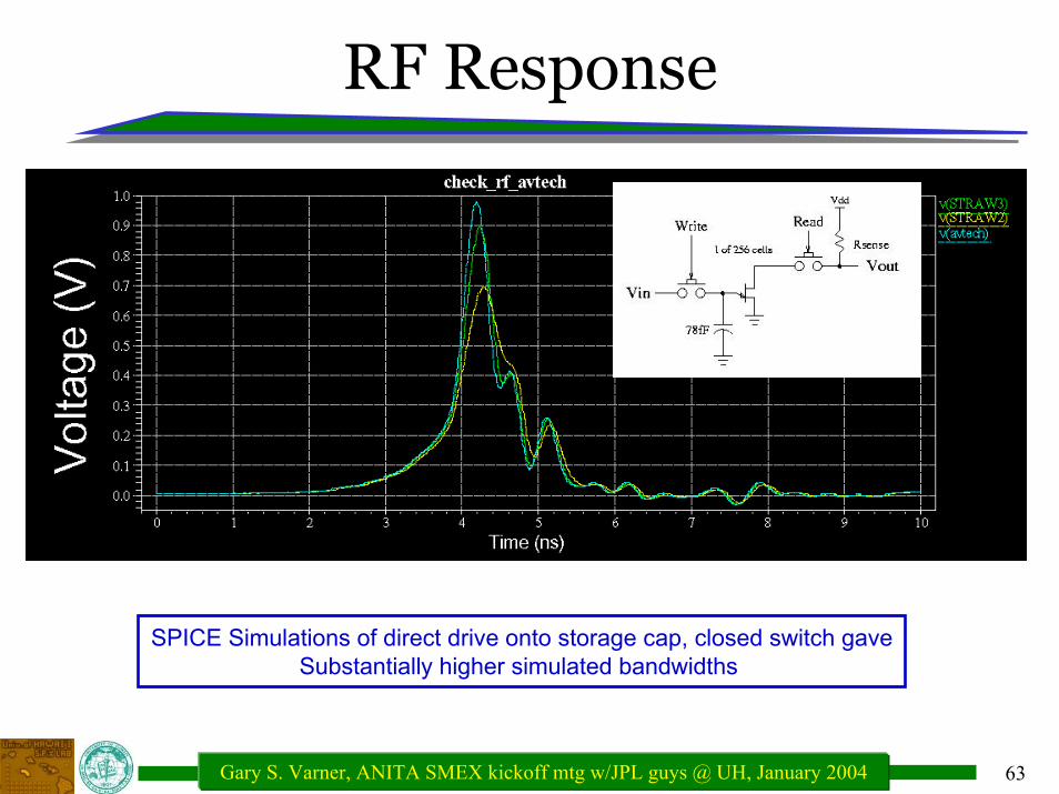
RF Response
SPICE Simulations of direct drive onto storage cap, closed switch gaveSubstantially higher simulated bandwidths
64Gary S. Varner, ANITA SMEX kickoff mtg w/JPL guys @ UH, January 2004
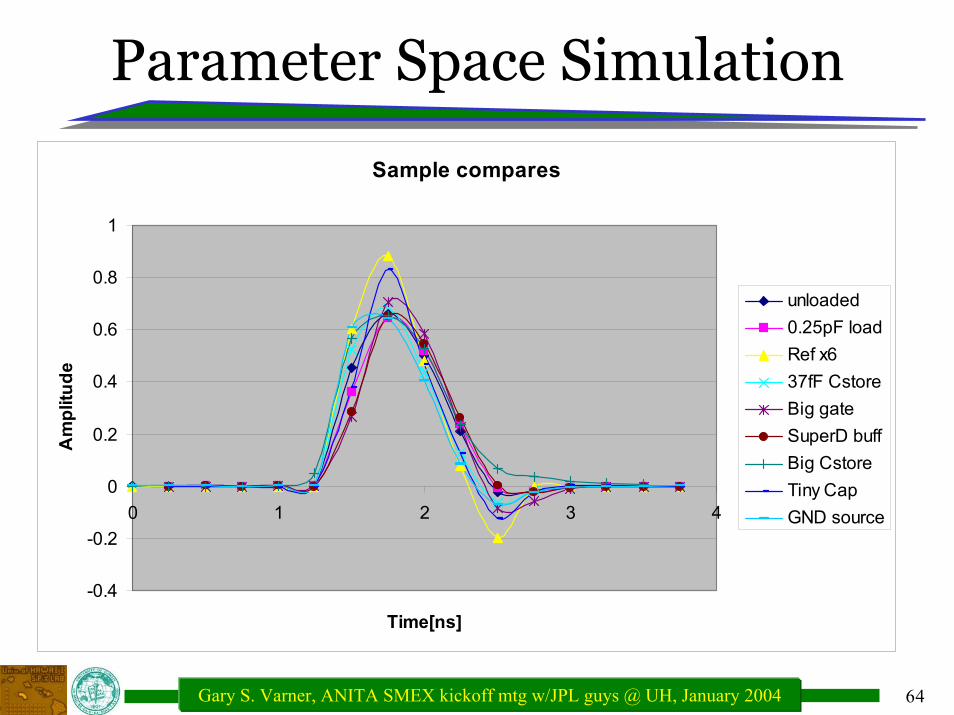
Parameter Space Simulation
Sample compares
-0.4
-0.2
0
0.2
0.4
0.6
0.8
1
0 1 2 3 4
Time[ns]
Am
plitu
de
unloaded0.25pF loadRef x637fF CstoreBig gateSuperD buffBig CstoreTiny CapGND source
65Gary S. Varner, ANITA SMEX kickoff mtg w/JPL guys @ UH, January 2004
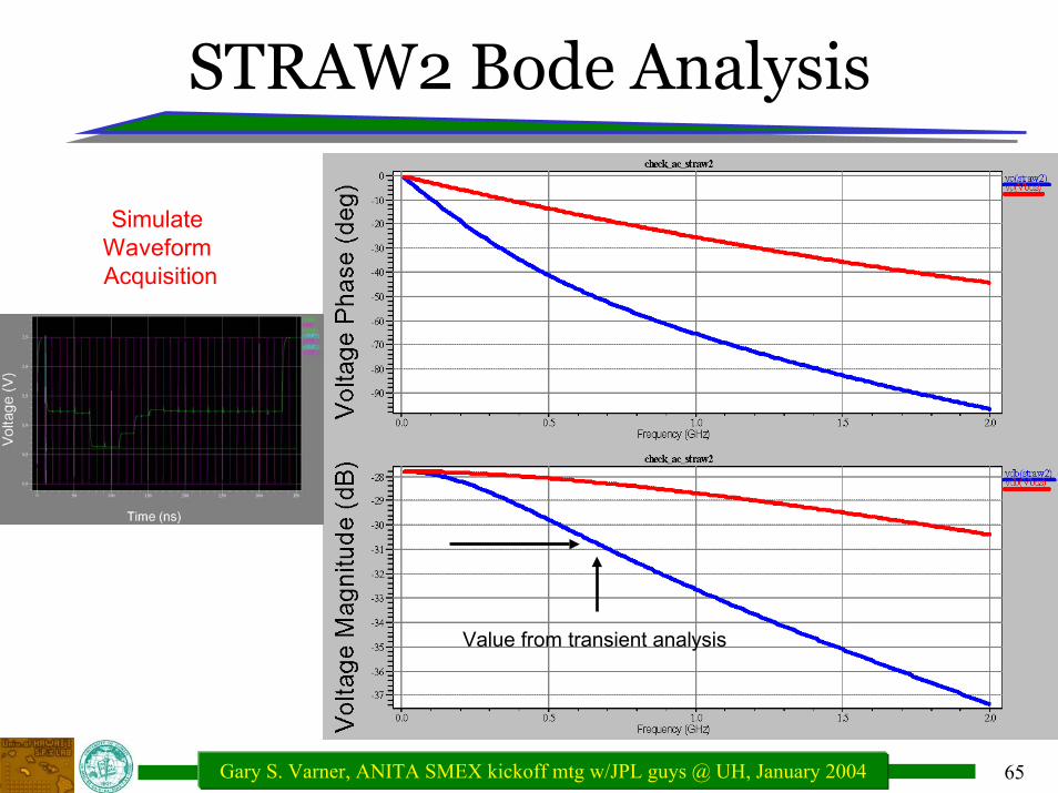
STRAW2 Bode Analysis
Value from transient analysis
Simulate Waveform Acquisition
66Gary S. Varner, ANITA SMEX kickoff mtg w/JPL guys @ UH, January 2004
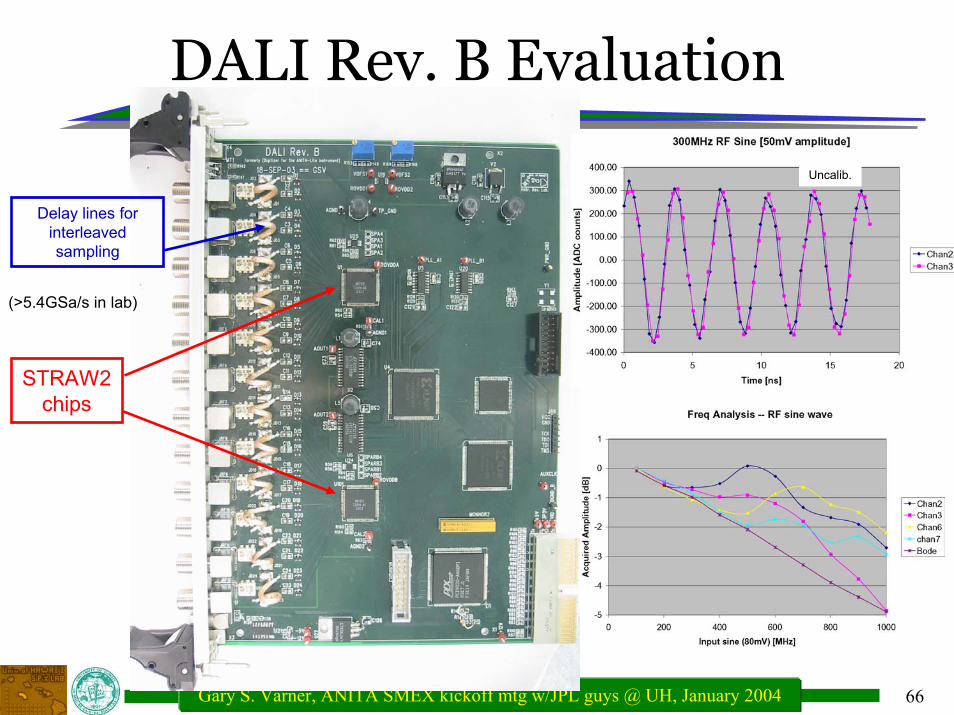
DALI Rev. B Evaluation
STRAW2chips
Delay lines for interleaved sampling
(>5.4GSa/s in lab)
Uncalib.
67Gary S. Varner, ANITA SMEX kickoff mtg w/JPL guys @ UH, January 2004
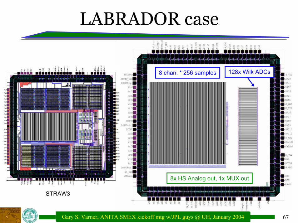
LABRADOR case
128x Wilk ADCs8 chan. * 256 samples
8x HS Analog out, 1x MUX out
STRAW3
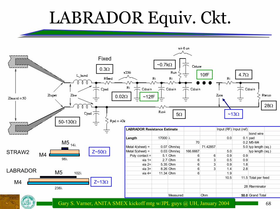
68Gary S. Varner, ANITA SMEX kickoff mtg w/JPL guys @ UH, January 2004
LABRADOR Equiv. Ckt.
5Ω
4.7Ω
28Ω
~13Ω
10fF
~0.7kΩ
~12fF0.02Ω
0.3Ω
50-130Ω
M5 14λ
Fixed
LABRADOR Resistance Estimate Input (RF) Input (ref)bond wire
Length 17000 λ 0.0 0.1 pad70 0.2 M5-M4
Metal 4(sheet) = 0.07 Ohm/sq 71.42857 5.0 typ length (sq.)Metal 5(sheet) = 0.03 Ohm/sq 166.6667 5.0 typ length (sq.)
Poly contact = 5.1 Ohm 6 6 0.9 0.9via 1= 2.7 Ohm 6 3 0.5 0.9via 2= 5.35 Ohm 6 3 0.9 1.8via 3= 8.26 Ohm 6 3 1.4 2.8via 4= 11.34 Ohm 6 1.9
10.5 11.5 Total per feed
28 Rterminator
Measured: Ohm 50.0 Grand Total
STRAW2 Z~50ΩM498λ
LABRADOR M5 102λ
M4 Z~13Ω238λ
69Gary S. Varner, ANITA SMEX kickoff mtg w/JPL guys @ UH, January 2004
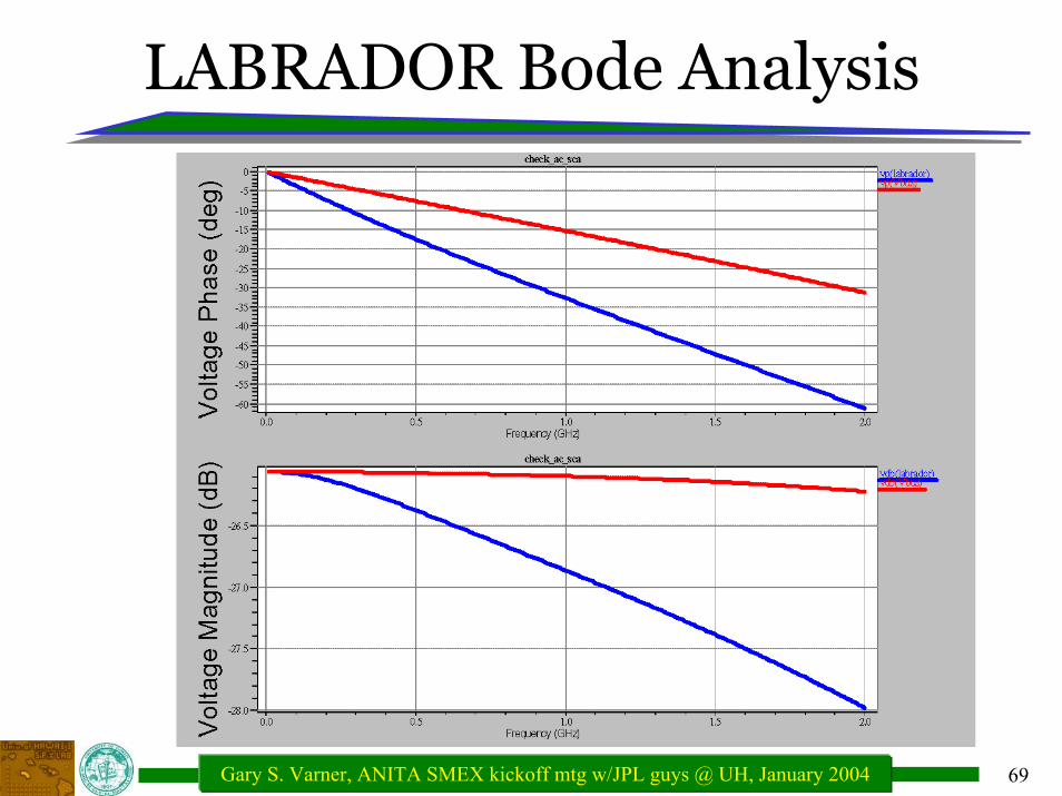
LABRADOR Bode Analysis
70Gary S. Varner, ANITA SMEX kickoff mtg w/JPL guys @ UH, January 2004
Current Status
• R&D into critical (non-standard) components:– Have a near-spec low-power sampler prototype
– Need for a custom trigger chip? (CF success of ALTO)
– Sufficiently low noise LNA? (low power enough?)
• Plans:– RFCeval board in debug – STRAW3 chip “alive”
– LABRADOR returns ~“now” (also test on RFCeval)
– cPCI interface development (DALI Rev. B)
• Discussion Items: (next slides)
ID Lab tour @ some point
71Gary S. Varner, ANITA SMEX kickoff mtg w/JPL guys @ UH, January 2004
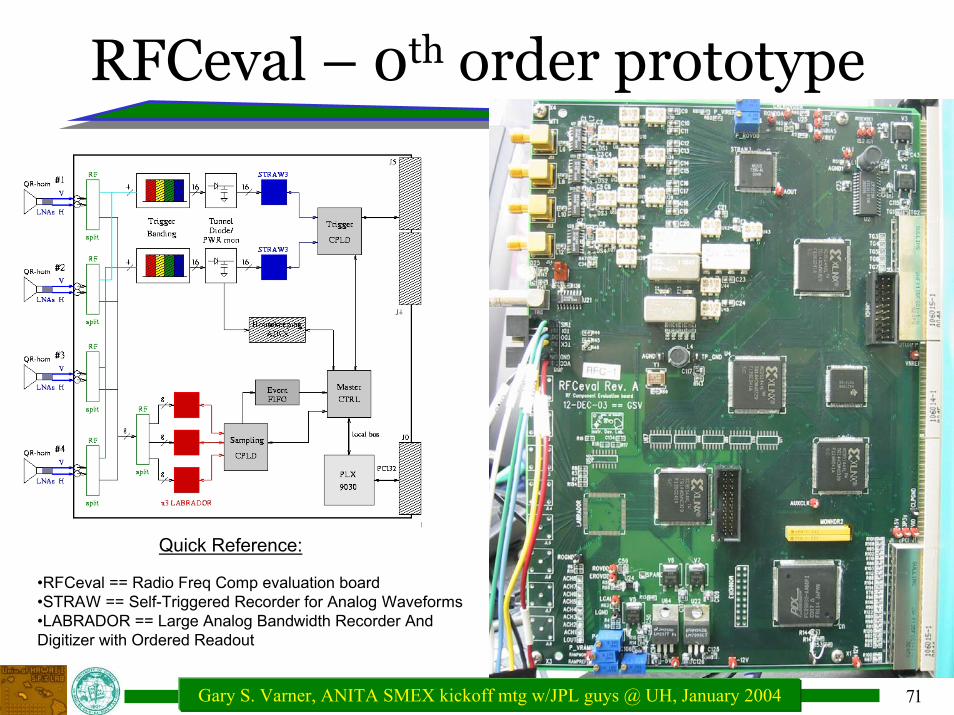
RFCeval – 0th order prototype
Quick Reference:
•RFCeval == Radio Freq Comp evaluation board•STRAW == Self-Triggered Recorder for Analog Waveforms•LABRADOR == Large Analog Bandwidth Recorder And Digitizer with Ordered Readout
72Gary S. Varner, ANITA SMEX kickoff mtg w/JPL guys @ UH, January 2004
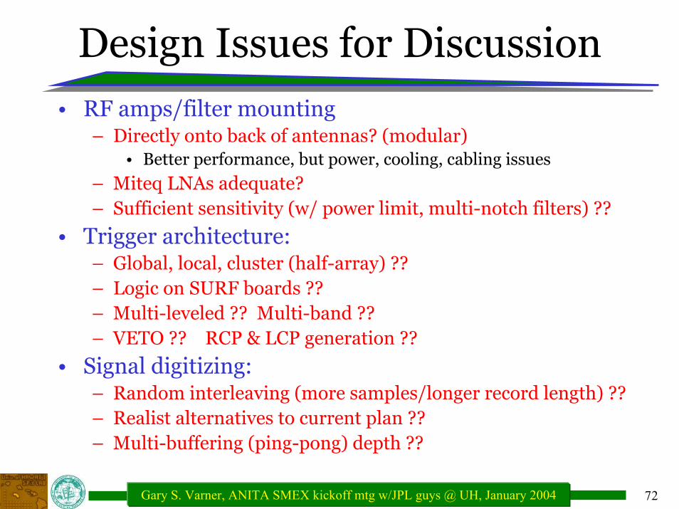
Design Issues for Discussion
• RF amps/filter mounting– Directly onto back of antennas? (modular)
• Better performance, but power, cooling, cabling issues
– Miteq LNAs adequate?– Sufficient sensitivity (w/ power limit, multi-notch filters) ??
• Trigger architecture:– Global, local, cluster (half-array) ??– Logic on SURF boards ??– Multi-leveled ?? Multi-band ??– VETO ?? RCP & LCP generation ??
• Signal digitizing:– Random interleaving (more samples/longer record length) ??– Realist alternatives to current plan ??– Multi-buffering (ping-pong) depth ??
73Gary S. Varner, ANITA SMEX kickoff mtg w/JPL guys @ UH, January 2004
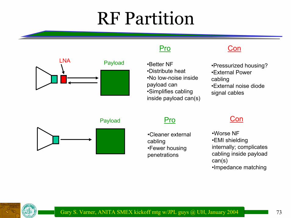
RF Partition
Pro ConLNA Payload •Better NF
•Distribute heat•No low-noise inside payload can•Simplifies cabling inside payload can(s)
•Pressurized housing?•External Power cabling•External noise diode signal cables
ConProPayload
•Worse NF•EMI shielding internally; complicates cabling inside payload can(s)•Impedance matching
•Cleaner external cabling•Fewer housing penetrations
74Gary S. Varner, ANITA SMEX kickoff mtg w/JPL guys @ UH, January 2004
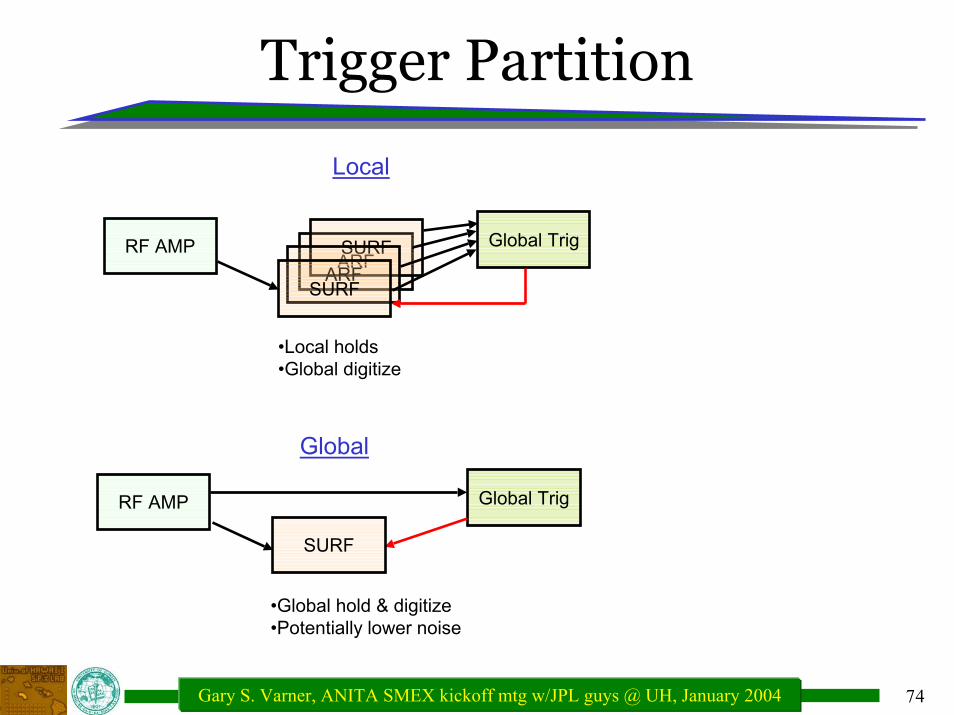
Trigger Partition
Local
ARFSURF
ARFSURF
Global TrigRF AMP
•Local holds•Global digitize
RF AMP
SURF
Global Trig
Global
•Global hold & digitize•Potentially lower noise
75Gary S. Varner, ANITA SMEX kickoff mtg w/JPL guys @ UH, January 2004
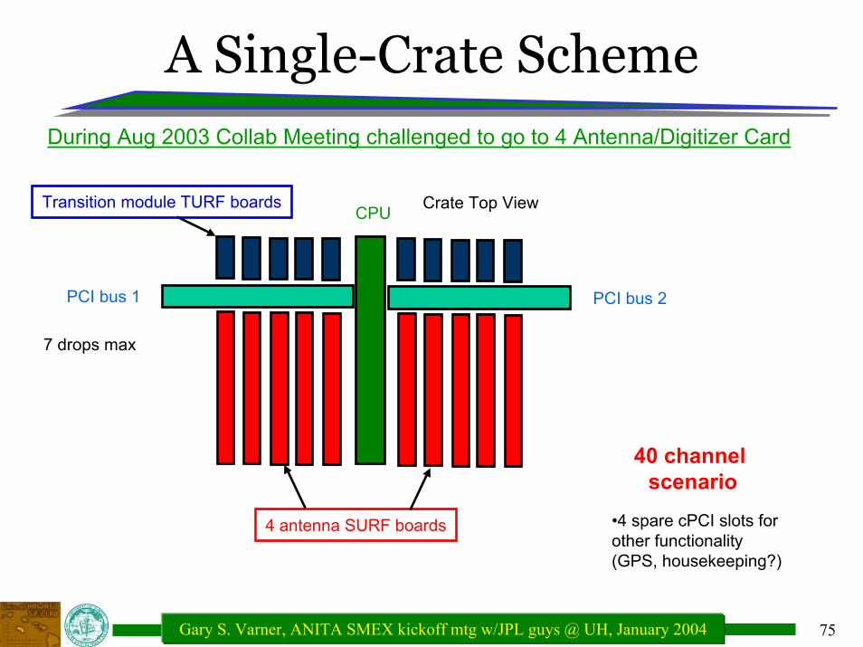
A Single-Crate SchemeDuring Aug 2003 Collab Meeting challenged to go to 4 Antenna/Digitizer Card
4 antenna SURF boards
Transition module TURF boards Crate Top ViewCPU
40 channel scenario
•4 spare cPCI slots for other functionality (GPS, housekeeping?)
PCI bus 1 PCI bus 2
7 drops max
76Gary S. Varner, ANITA SMEX kickoff mtg w/JPL guys @ UH, January 2004
WBS Impacts
• Forgotten issues?
• Specification for overall Power Max?
• Plans:– Milestones?
– Hardware Task sharing (suboptimal in ANITA-lite)
77Gary S. Varner, ANITA SMEX kickoff mtg w/JPL guys @ UH, January 2004
Back-up slides
78Gary S. Varner, ANITA SMEX kickoff mtg w/JPL guys @ UH, January 2004
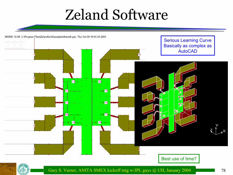
Zeland Software
Serious Learning CurveBasically as complex as
AutoCAD
Best use of time?
79Gary S. Varner, ANITA SMEX kickoff mtg w/JPL guys @ UH, January 2004
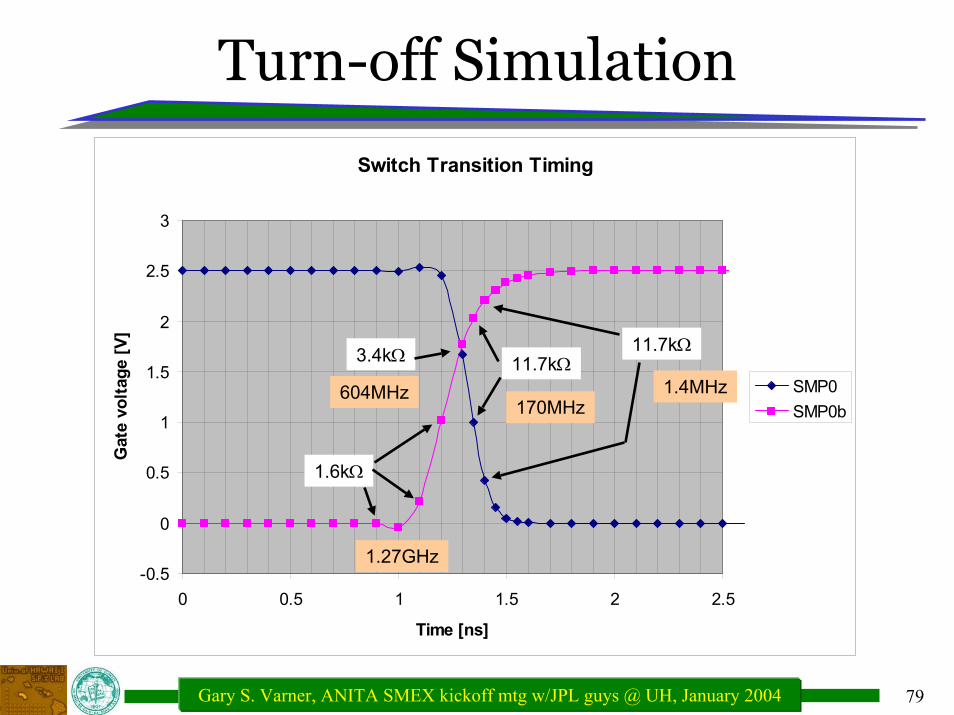
Turn-off Simulation
Switch Transition Timing
-0.5
0
0.5
1
1.5
2
2.5
3
0 0.5 1 1.5 2 2.5
Time [ns]
Gat
e vo
ltage
[V]
SMP0SMP0b
1.27GHz
1.6kΩ
3.4kΩ
604MHz11.7kΩ
170MHz
11.7kΩ
1.4MHz
80Gary S. Varner, ANITA SMEX kickoff mtg w/JPL guys @ UH, January 2004
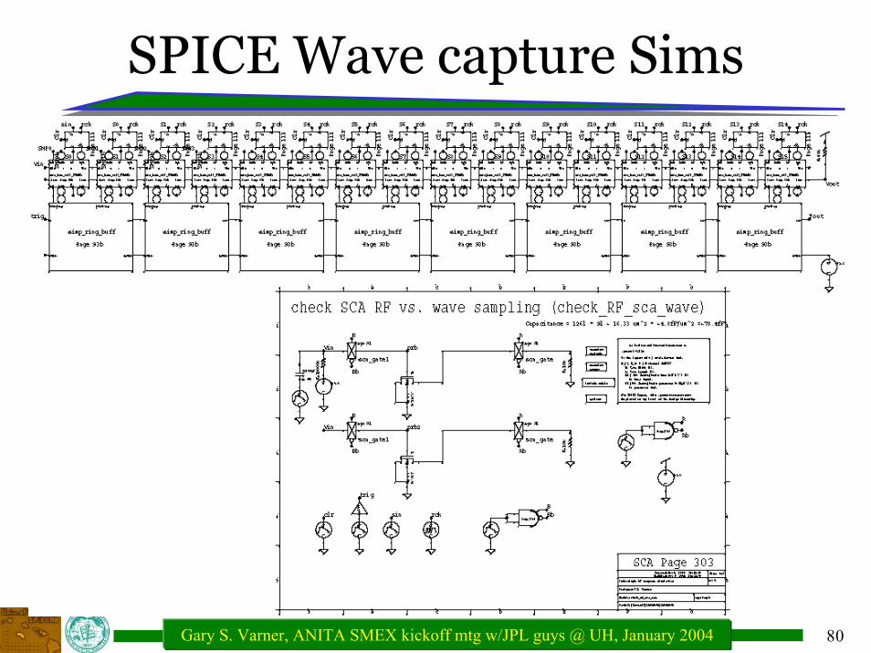
SPICE Wave capture Sims
81Gary S. Varner, ANITA SMEX kickoff mtg w/JPL guys @ UH, January 2004
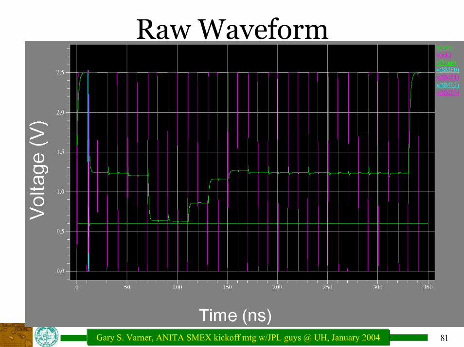
Raw Waveform
82Gary S. Varner, ANITA SMEX kickoff mtg w/JPL guys @ UH, January 2004
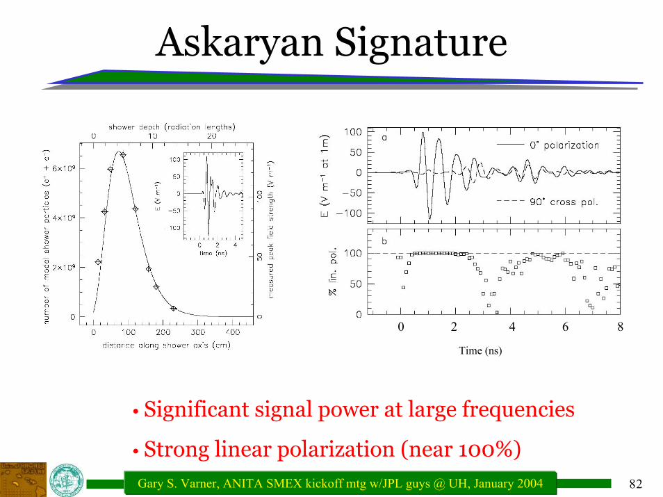
Askaryan Signature
0 2 4 6 8
Time (ns)
• Significant signal power at large frequencies
• Strong linear polarization (near 100%)
83Gary S. Varner, ANITA SMEX kickoff mtg w/JPL guys @ UH, January 2004
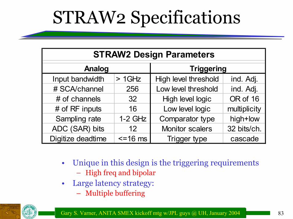
STRAW2 Specifications
> 1GHz ind. Adj.256 ind. Adj.32 OR of 1616 multiplicity
1-2 GHz high+low12 32 bits/ch.
<=16 ms cascadeADC (SAR) bits
Digitize deadtime
High level thresholdLow level threshold
High level logicLow level logic
Comparator typeMonitor scalers
Trigger type
# SCA/channel# of channels# of RF inputsSampling rate
Analog Triggering
STRAW2 Design Parameters
Input bandwidth
• Unique in this design is the triggering requirements – High freq and bipolar
• Large latency strategy:– Multiple buffering
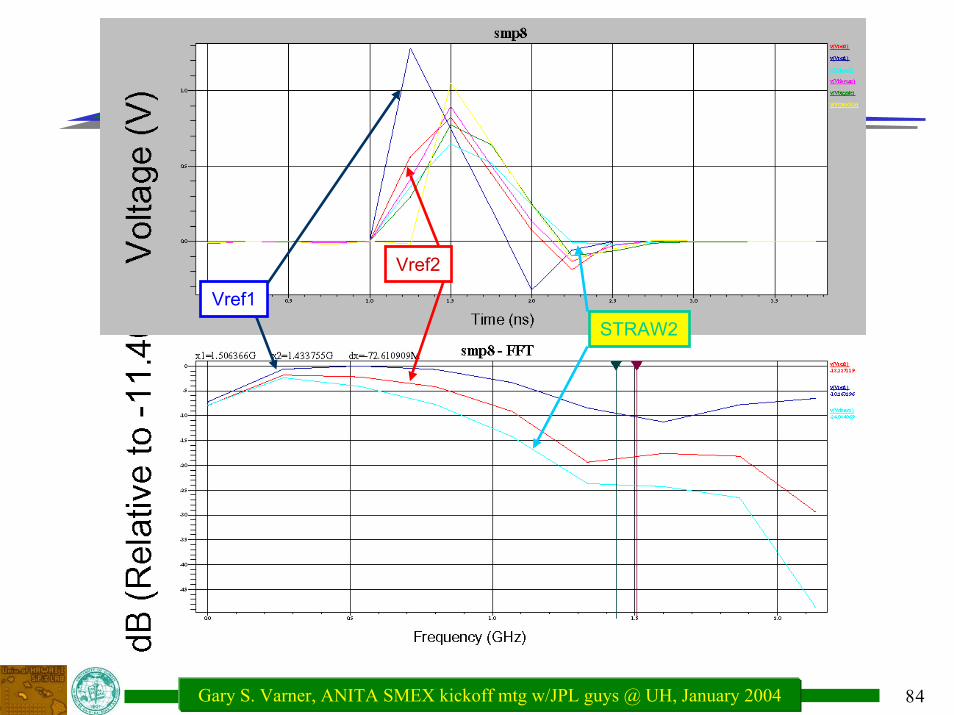
84Gary S. Varner, ANITA SMEX kickoff mtg w/JPL guys @ UH, January 2004
FFT curves
Vref1
Vref2
STRAW2
85Gary S. Varner, ANITA SMEX kickoff mtg w/JPL guys @ UH, January 2004
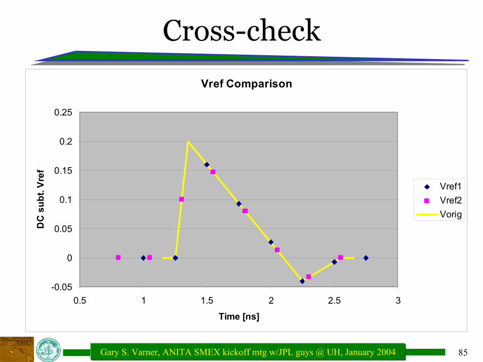
Cross-check
Vref Comparison
-0.05
0
0.05
0.1
0.15
0.2
0.25
0.5 1 1.5 2 2.5 3
Time [ns]
DC
sub
t. Vr
ef
Vref1Vref2Vorig
86Gary S. Varner, ANITA SMEX kickoff mtg w/JPL guys @ UH, January 2004
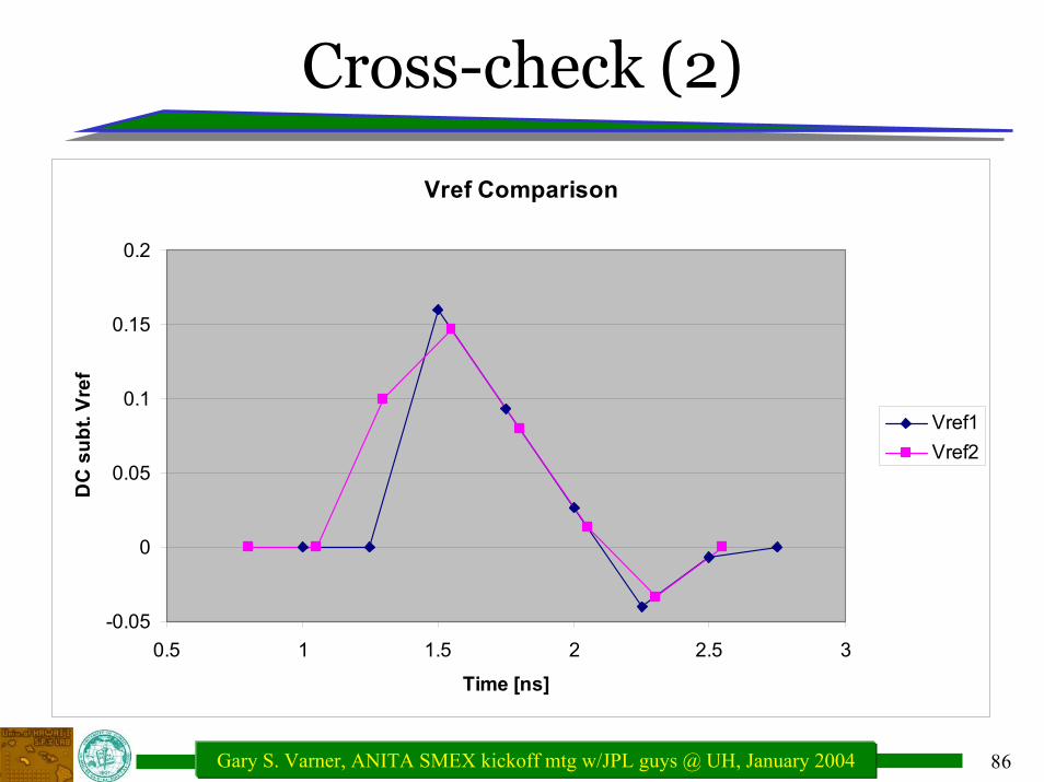
Cross-check (2)
Vref Comparison
-0.05
0
0.05
0.1
0.15
0.2
0.5 1 1.5 2 2.5 3
Time [ns]
DC
sub
t. Vr
ef
Vref1Vref2
87Gary S. Varner, ANITA SMEX kickoff mtg w/JPL guys @ UH, January 2004
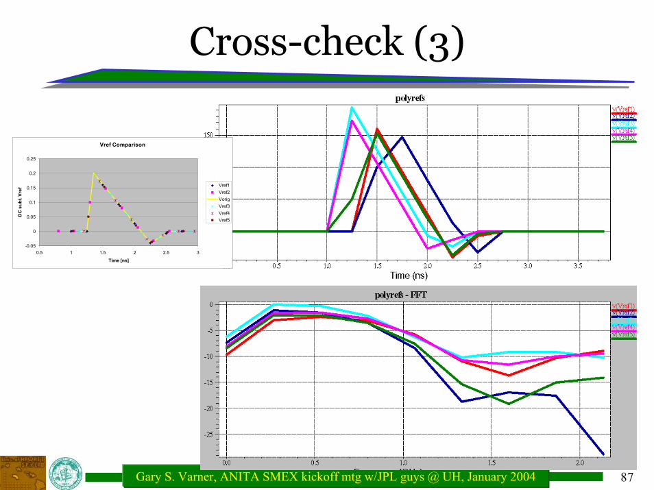
Cross-check (3)
Vref Comparison
-0.05
0
0.05
0.1
0.15
0.2
0.25
0.5 1 1.5 2 2.5 3
Time [ns]
DC
sub
t. Vr
ef
Vref1Vref2VorigVref3Vref4Vref5
88Gary S. Varner, ANITA SMEX kickoff mtg w/JPL guys @ UH, January 2004
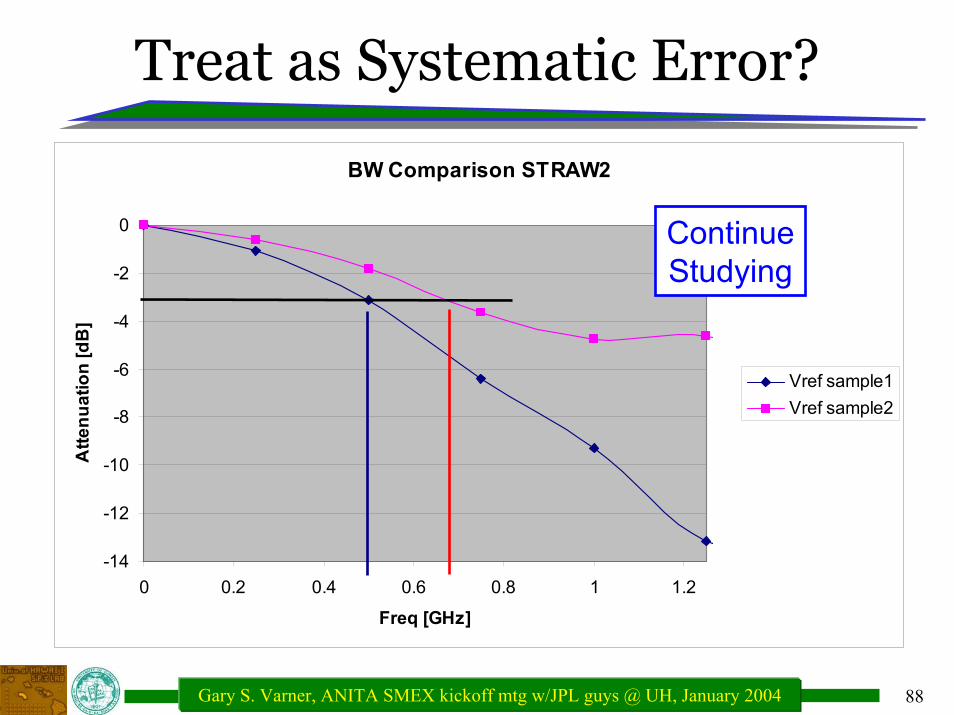
Treat as Systematic Error?
BW Comparison STRAW2
-14
-12
-10
-8
-6
-4
-2
0
0 0.2 0.4 0.6 0.8 1 1.2
Freq [GHz]
Atte
nuat
ion
[dB
]
Vref sample1Vref sample2
ContinueStudying
89Gary S. Varner, ANITA SMEX kickoff mtg w/JPL guys @ UH, January 2004
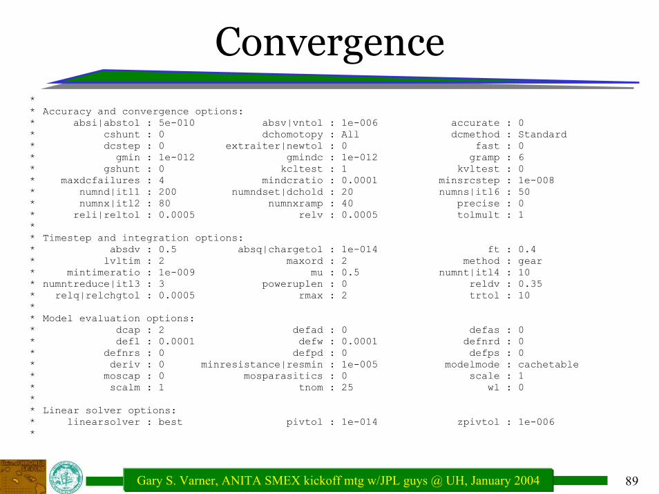
Convergence** Accuracy and convergence options:* absi|abstol : 5e-010 absv|vntol : 1e-006 accurate : 0* cshunt : 0 dchomotopy : All dcmethod : Standard* dcstep : 0 extraiter|newtol : 0 fast : 0* gmin : 1e-012 gmindc : 1e-012 gramp : 6* gshunt : 0 kcltest : 1 kvltest : 0* maxdcfailures : 4 mindcratio : 0.0001 minsrcstep : 1e-008* numnd|itl1 : 200 numndset|dchold : 20 numns|itl6 : 50* numnx|itl2 : 80 numnxramp : 40 precise : 0* reli|reltol : 0.0005 relv : 0.0005 tolmult : 1** Timestep and integration options:* absdv : 0.5 absq|chargetol : 1e-014 ft : 0.4* lvltim : 2 maxord : 2 method : gear* mintimeratio : 1e-009 mu : 0.5 numnt|itl4 : 10* numntreduce|itl3 : 3 poweruplen : 0 reldv : 0.35* relq|relchgtol : 0.0005 rmax : 2 trtol : 10** Model evaluation options:* dcap : 2 defad : 0 defas : 0* defl : 0.0001 defw : 0.0001 defnrd : 0* defnrs : 0 defpd : 0 defps : 0* deriv : 0 minresistance|resmin : 1e-005 modelmode : cachetable* moscap : 0 mosparasitics : 0 scale : 1* scalm : 1 tnom : 25 wl : 0** Linear solver options:* linearsolver : best pivtol : 1e-014 zpivtol : 1e-006*
90Gary S. Varner, ANITA SMEX kickoff mtg w/JPL guys @ UH, January 2004
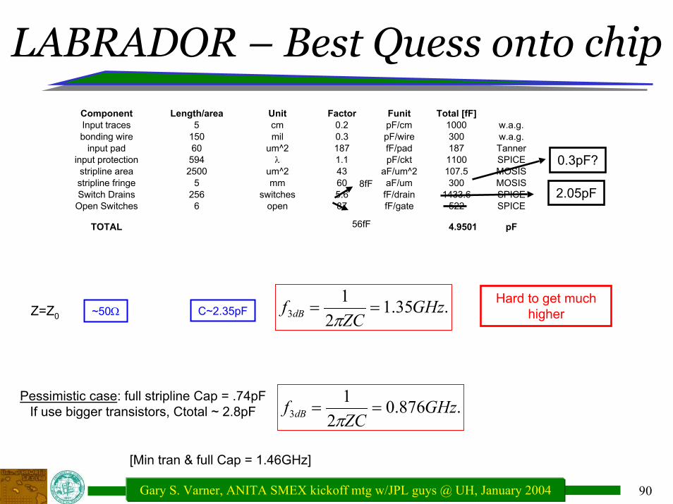
LABRADOR – Best Quess onto chip
Component Length/area Unit Factor Funit Total [fF]Input traces 5 cm 0.2 pF/cm 1000 w.a.g.bonding wire 150 mil 0.3 pF/wire 300 w.a.g.
input pad 60 um^2 187 fF/pad 187 Tannerinput protection 594 λ 1.1 pF/ckt 1100 SPICEstripline area 2500 um^2 43 aF/um^2 107.5 MOSISstripline fringe 5 mm 60 aF/um 300 MOSISSwitch Drains 256 switches 5.6 fF/drain 1433.6 SPICE
Open Switches 6 open 87 fF/gate 522 SPICE
TOTAL 4.9501 pF56fF
8fF
.35.12
13 GHz
ZCf dB ==
πHard to get much
higherZ=Z0 ~50Ω C~2.35pF
0.3pF?
2.05pF
.876.02
13 GHz
ZCf dB ==
πPessimistic case: full stripline Cap = .74pF
If use bigger transistors, Ctotal ~ 2.8pF
[Min tran & full Cap = 1.46GHz]
91Gary S. Varner, ANITA SMEX kickoff mtg w/JPL guys @ UH, January 2004
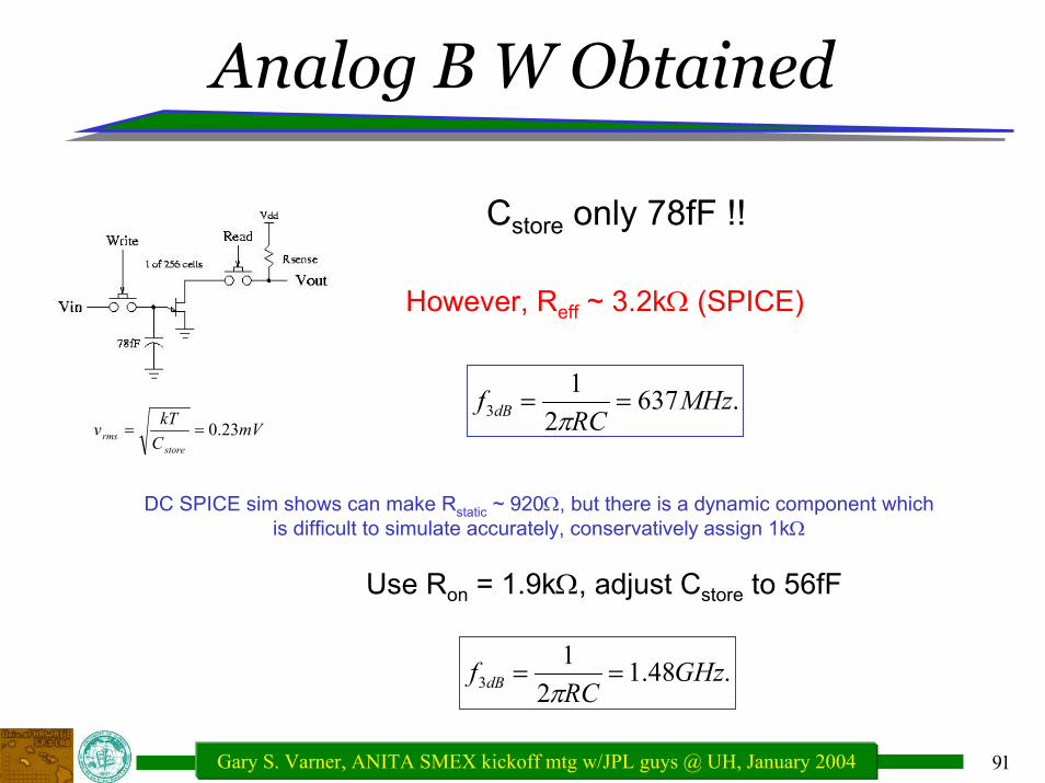
Analog B W Obtained
Cstore only 78fF !!
However, Reff ~ 3.2kΩ (SPICE)
.6372
13 MHz
RCf dB ==
πmVCkTvstore
rms 23.0==
DC SPICE sim shows can make Rstatic ~ 920Ω, but there is a dynamic component which is difficult to simulate accurately, conservatively assign 1kΩ
Use Ron = 1.9kΩ, adjust Cstore to 56fF
.48.12
13 GHz
RCf dB ==
π