Andrei Nomerotski 1 Instrumentation for Medical Applications Andrei Nomerotski (Oxford Particle...
36
Andrei Nomerotski 1 Instrumentation for Medical Applications Andrei Nomerotski (Oxford Particle Physics) VC Forum, 17 November 2009
-
date post
19-Dec-2015 -
Category
Documents
-
view
224 -
download
0
Transcript of Andrei Nomerotski 1 Instrumentation for Medical Applications Andrei Nomerotski (Oxford Particle...

Andrei Nomerotski
1
Instrumentation for Medical Applications
Andrei Nomerotski (Oxford Particle Physics)
VC Forum, 17 November 2009

Andrei Nomerotski
2
Particle Detectors in Medicine Energy scales of modern particle physics are much
beyond needs of medicine but detection techniques are similar High energy particles cascade to low energy particles
Detection of visible light and X-rays is in demand both in medical imaging and particle physics
Medical imaging Slow rates (~Hz) Modest # of frames per second Complicated processing Each frame is a lot of information High data rates

Andrei Nomerotski
3
Driving Factors Huge progress in micro (nano) electronics
New silicon technologies New types of detectors
Complicated processing at sensor level
New materials
Computing faster CPU Taking advantage of Moore’s law Software sophistication

Andrei Nomerotski
4
Outline
In the following will talk about
Positron Emission Tomography
Medical Imaging using silicon detectors
In Vivo Dosimetry

Andrei Nomerotski
5
Positron Emission Tomography (PET)
5
• Cancer diagnostic tool
• Distinguish normal and cancerous tissue on the basis of their biological function

Andrei Nomerotski
6
FDG-PET: basic principle
Two opposite PET detectors operating in coincidence
511 keV
511 keV -ray
511 keV -ray
18F-fluoro-deoxy-glucose

Andrei Nomerotski
7
Whole Body PET
Usually combined with Computer Tomography (CT)
PET accuracy ~5 mm Overlaid images give better accuracy CT allow for attenuation corrections
2M scans annually 20% per year growth

Andrei Nomerotski
8
Scintillator:Converts 511 keV gamma-rays into the light
PMTs: Convert the scintillation light into a measurable electrical voltage pulse
511 keVgamma-rays
8
PET detector componentsPET detector components

Andrei Nomerotski
9
Solid-State PET Detectors
• Avalanche photodiode (APD)
High detection efficiency (~50%)
Wide dynamic range
Low gain (~100)
• Silicon Photomultiplier (SiPM)
Work in Geiger mode
Gain is comparable to PMTs (~106)
High speed (similar to PMTs)
Limited dynamic range
Bein
g c
onsi
dere
dA
lready d
evelo
ped

Andrei Nomerotski
10
Silicon Photomultiplier (SiPM)
SiPM devices SiPM microcells
Schematic diagram
1mm x 1mm
HAMAMATSU Inc.
• Geiger mode operated silicon arrays on a common substrate• Invented in 90’s• Last years – big improvements in parameters and available bareas

Andrei Nomerotski
11
Silicon Photomultiplier
Hamamatsu MPPC

Andrei Nomerotski
12
New Fast Scintillators
Promising new scintillators: PreLudeTM420 (LYSO) and BrilLanCeTM380 (LaBr3(Ce)) By Saint-Gobain Cristaux et Detecteurs

Andrei Nomerotski
13
Time Of Flight PET
Use time information to localize interaction with ~few cm precision
Allows for better image quality for same dose
Or lower dose (=higher throughput) for same image quality
Need to achieve ~100 ps timing accuracy
Currently ~400 ps
Andrei Nomerotski
14
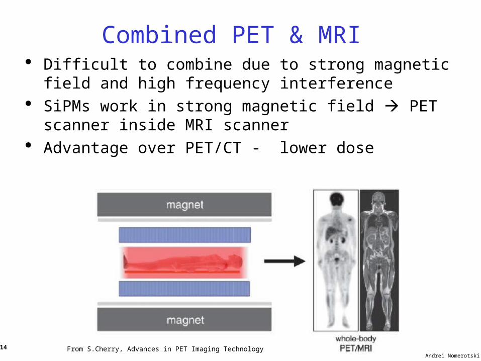
Combined PET & MRI Difficult to combine due to strong magnetic field and high
frequency interference SiPMs work in strong magnetic field PET scanner inside
MRI scanner Advantage over PET/CT - lower dose
From S.Cherry, Advances in PET Imaging Technology

Andrei Nomerotski
15
PET R&D Activities in Oxford Physics Ongoing R&D on SiPM can be used for
PET
Preparing a bid to Wellcome/STFC to build a TOF-PET demonstrator
Discussing common R&D projects with Churchill
Offer SiPM/TOF-PET MPhys project in Physics

Andrei Nomerotski
16
Medical Imaging

Andrei Nomerotski
17
Medical Imaging Concentrate on X-ray imaging with silicon detectors Nicely demonstrates advances in silicon industry
Not driven by science any more rather by telecommunications and PlayStation users
Nowadays use processes with 0.09 m = 90 nm min feature size with 45 nm in sight
Medipix – silicon pixel detector with integrated electronics and readout Started at CERN in 90’s as by-product of R&D for future
LHC experiments Very successful with dozens of applications outside of PP
(and medicine)

Andrei Nomerotski
18
X-Rays in Silicon Visible photon range few m 20keV X-ray range 5 m 100 keV X-ray range 80 m For larger energies need different materials (higher Z)

Andrei Nomerotski
19
Hybrid-Pixel DetectorsHybrid-Pixel Detectors
p+
n-
ASICn-well
p-substrate
Semiconductor detector
Bump-bond contact
Charged particle
gm
Iin Vout
Pulse processing electronics provides simultaneously fast and noise free images

Andrei Nomerotski
20
Medipix2 Bump BondingMedipix2 Bump Bonding

Andrei Nomerotski
21
Preamp
Disc1
Disc2
Double Disc logic
Vth Low
Vth High
13 bits
Shift Register
Input
Ctest
Testbit
Test Input
Maskbit
Maskbit
3 bits threshold
3 bits threshold
Shutter
Mux
Mux
ClockOut
Previous Pixel
Next Pixel
Conf
8 bits configuration
Polarity
Analog Digital
Preamp
Disc1
Disc2
Double Disc logic
Vth Low
Vth High
13 bits
Shift Register
Input
Ctest
Testbit
Test Input
Maskbit
Maskbit
3 bits threshold
3 bits threshold
Shutter
Mux
Mux
ClockOut
Previous Pixel
Next Pixel
Conf
8 bits configuration
Polarity
Analog Digital
Charge sensitive preamplifier with individual leakage current compensation
2 discriminators with globally adjustable threshold
3-bit local fine tuning of the threshold per discriminator
1 test and 1 mask bit
External shutter activates the counter
13-bit counter
1 Overflow bit
Signal ~ few 1000 electrons (!)
Medipix2 Pixel Cell SchematicMedipix2 Pixel Cell Schematic

Andrei Nomerotski
22
Medipix2 Cell LayoutMedipix2 Cell Layout
55 m
55 m
55 m
55 m

Andrei Nomerotski
23
Medipix2 Chip ArchitectureMedipix2 Chip Architecture
IO
Logic
LVDS
Input
LVDS
Output32-bi t C MOS Output
256-bi t Fast Shift Register
3328
-bit
Pix
el C
olum
n-0
13 8-bi t DACs
14111 m
3328
-bit
Pix
el C
olum
n-1
3328
-bit
Pix
el C
olum
n-1
1612
0
m
IO
Logic
LVDS
Input
LVDS
Output32-bi t C MOS Output
256-bi t Fast Shift Register
3328
-bit
Pix
el C
olum
n-0
13 8-bi t DACs
14111 m
3328
-bit
Pix
el C
olum
n-1
3328
-bit
Pix
el C
olum
n-1
1612
0
m
256 x 256 pixels
5ms readout time(serial @ 200MHz)
300s readout time (parallel @ 100MHz)

Andrei Nomerotski
24
Medipix Data Acquisition
Max frame rates ~ 1 kHz USB interface- easy to use
X-ray detector
Medipix with USB interface

Andrei Nomerotski
25
Sample ImagesSample Images

Andrei Nomerotski
26
High resolution X-ray imaging using a micro-High resolution X-ray imaging using a micro-focus X-ray sourcefocus X-ray source
Needle holding the sample
Edges are enhanced by phase contrast effect
S. Pospisil, J. Jakubek and co-workers, IEAP, CTU, Prague, CZ
Andrei Nomerotski
27
Future Trends
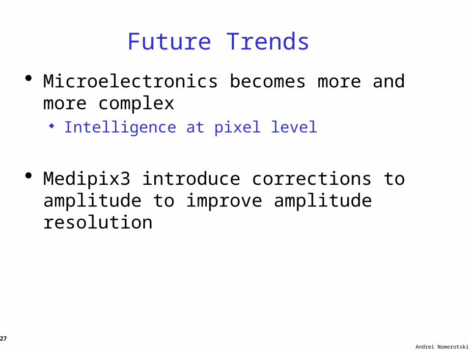
Microelectronics becomes more and more complex Intelligence at pixel level
Medipix3 introduce corrections to amplitude to improve amplitude resolution

Andrei Nomerotski
28
Charge summing and allocation concept
55µm
The winner takes all

Andrei Nomerotski
29
Medipix3 SimulationMedipix3 Simulation
Much improved amplitude resolution Immune to threshold variations

Andrei Nomerotski
30
Material Reconstruction in CTMaterial Reconstruction in CT
Photon counting at8 keV threshold
water /non iodine
iodine
Brightness = density of materials (g/cm3)
Measurements in collaboration with the University of Canterbury, Christchurch
G. Anton, T. Michel and co-workers, Univ. Erlangen, D
Amplitude information important to distinguish between different materials

Andrei Nomerotski
31
In Vivo Dosimetry A lot of interest given JAI activities on
therapy of cancer using particle accelerators
TLD, diodes, MOSFETs TLDs are complicated to process Diodes need a cable and continuous
readout New: MOSFET
Metal Oxide Semiconductor Field Effect Transistors
Absorbed dose change characteristics of MOSFET
Compact ~1 mm
Much needed instrument with a lot of room for improvement and new ideas
scanditronix-wellhofer.com

Andrei Nomerotski
32
Medipix Activities in Oxford Area Several Medipix/Timepix users
Diamond Light Source for crystal diffraction studies Oxford Chemistry/Physics for Ion Imaging Mass
Spectrometry Oxford Engineering for Mammography
Talking to each other, may think about joining the Medipix collaboration

Andrei Nomerotski
33
Future: Monolithic Sensors
Future trend is in integration of detector and electronics in one sensor, MAPS (Monolithic Active Pixel Sensor)
Pixels
Bump Bonds
Readout Electronics

Andrei Nomerotski
34
Monolithic Sensors with 3D Integration
Technologies becoming available to thin silicon wafers to 10 microns and to bond them together
New approach to monolithic sensors: 3D integration Precision 1 m alignment Interconnection of wafers by metal vias
Opto Electronics
Digital layer
Analog Layer
Sensor Layer
Optical Fiber I n Optical Fiber Out
Designer’s Dream
50 um

Andrei Nomerotski
35
Ultra Thin Devices First attempts to produce ultra-thin devices in industry and for
particle detection are under way hopefully will make its way to medical applications as well

Andrei Nomerotski
36
Summary Enormous progress in detector technologies and
nanoelectronics which can be applied to medical applications Especially to imaging
A lot of interest from Physics side to apply better detectors to medicine
Medical applications are driven by practical needs and economics benefit from communications between two communities
Acknowledgements: Medipix collaboration