Andes Embedded Processors Andes Embedded...
38
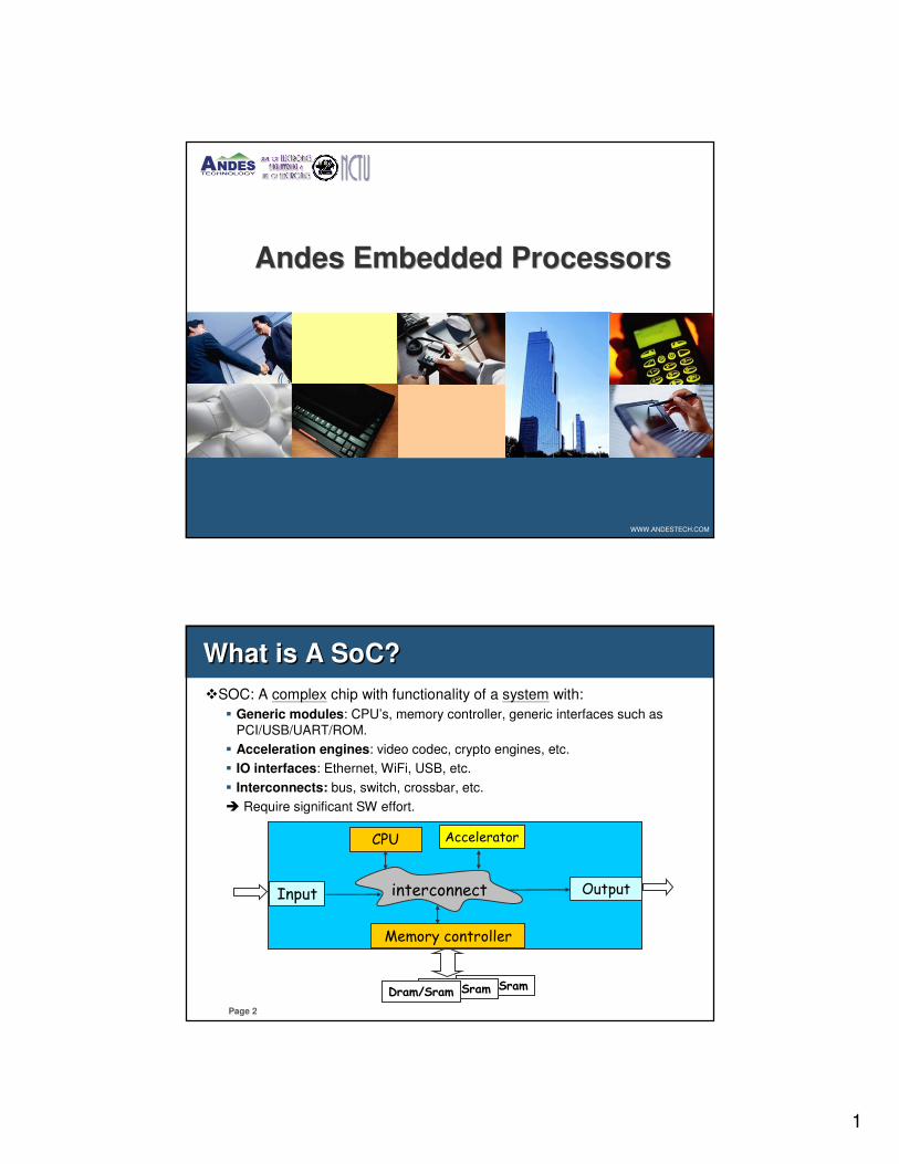
1 WWW.ANDESTECH.COM Andes Embedded Processors Andes Andes Embedded Processors Embedded Processors Page 2 What is A SoC? What is A SoC? SOC: A complex chip with functionality of a system with: Generic modules: CPU’s, memory controller, generic interfaces such as PCI/USB/UART/ROM. Acceleration engines: video codec, crypto engines, etc. IO interfaces: Ethernet, WiFi, USB, etc. Interconnects: bus, switch, crossbar, etc. Require significant SW effort. CPU Input Output Accelerator interconnect Memory controller Dram/Sram Dram/Sram Dram/Sram
Transcript of Andes Embedded Processors Andes Embedded...
1
WWW.ANDESTECH.COM
Andes Embedded Processors Andes Andes Embedded Processors Embedded Processors
Page 2
What is A SoC?What is A SoC?
�SOC: A complex chip with functionality of a system with:
� Generic modules: CPU’s, memory controller, generic interfaces such as
PCI/USB/UART/ROM.
� Acceleration engines: video codec, crypto engines, etc.
� IO interfaces: Ethernet, WiFi, USB, etc.
� Interconnects: bus, switch, crossbar, etc.
� Require significant SW effort.
CPU
Input Output
Accelerator
interconnect
Memory controller
Dram/SramDram/SramDram/Sram
2
Page 3
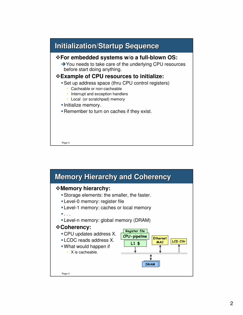
Initialization/Startup SequenceInitialization/Startup Sequence
�For embedded systems w/o a full-blown OS:�You needs to take care of the underlying CPU resources
before start doing anything.
�Example of CPU resources to initialize:�Set up address space (thru CPU control registers)
• Cacheable or non-cacheable
• Interrupt and exception handlers
• Local (or scratchpad) memory
� Initialize memory.
�Remember to turn on caches if they exist.
Page 4
Memory Hierarchy and CoherencyMemory Hierarchy and Coherency
�Memory hierarchy:�Storage elements: the smaller, the faster.
�Level-0 memory: register file
�Level-1 memory: caches or local memory
� . . .
�Level-n memory: global memory (DRAM)
�Coherency:�CPU updates address X.
�LCDC reads address X.
�What would happen if• X is cacheable.
CPU-pipelineRegister file
LCD CtlrEthernet
MAC
DRAMDRAM
L1 $

3
Page 5
Peripheral Control and DMAPeripheral Control and DMA
� How to control a peripheral (or a device)?� Thru control/status registers� SW controlling peripherals: device drivers
� Example: LCD controller (LCDC)� Preparation: CPU sets display’s resolution� Periodic data transfer
• scheme 1: CPU involved in all work– CPU reads each pixel from frame buffer and writes it to LCDC’s display
register.• scheme 2: CPU initiating the work
– CPU sets frame buffer’s base address.– CPU sets “GO” bit to start the whole operation, where LCDC reads frame
buffer data automatically and periodically.
� Status:• Record error status (e.g. data can’t arrive at LCDC on time).
� DMA: scheme 2� Free CPU to do something else
• after setting up batch job.
Page 6
ADP-XC5FF676 Main Board OverviewADP-XC5FF676 Main Board Overview
RJ45
VIRTEX
LED
GPIO Push
Buttons
UARTs
Audio Phone Jack
DC-IN Jack
SDRAM
Reset Button
Flash
Oscillator
SD/MMC
Nor Flash
Power Switch
AHB
Connector
MII
Connector
LCM
ConnectorEBI/X-BUS
A-ICE Connector
Power On
Button
4
Page 7
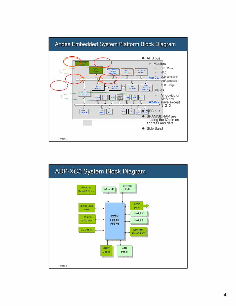
Andes Embedded System Platform Block DiagramAndes Embedded System Platform Block Diagram
Customerdesign
NCORE
INCTRL
CPU
Core
� AHB bus
� Masters
• CPU Core
• MAC
• LCD controller
• DMA controller
• APB Bridge
� Slaves
• All device on AHB are slave except N1213
� APB bus
� SRAM/SDRAM are sharing the IO pin on address and data
� Side Band
Page 8
ADP-XC5 System Block DiagramADP-XC5 System Block Diagram
5
Page 9
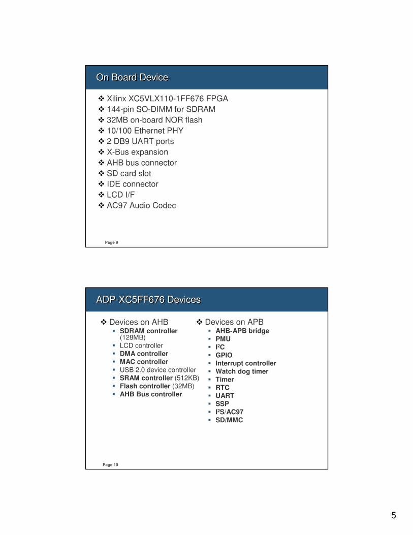
On Board DeviceOn Board Device
� Xilinx XC5VLX110-1FF676 FPGA
� 144-pin SO-DIMM for SDRAM
� 32MB on-board NOR flash
� 10/100 Ethernet PHY
� 2 DB9 UART ports
� X-Bus expansion
� AHB bus connector
� SD card slot
� IDE connector
� LCD I/F
� AC97 Audio Codec
Page 10
ADP-XC5FF676 DevicesADP-XC5FF676 Devices
� Devices on AHB� SDRAM controller
(128MB)
� LCD controller
� DMA controller
� MAC controller
� USB 2.0 device controller
� SRAM controller (512KB)
� Flash controller (32MB)
� AHB Bus controller
� Devices on APB� AHB-APB bridge
� PMU
� I2C
� GPIO
� Interrupt controller
� Watch dog timer
� Timer
� RTC
� UART
� SSP
� I2S/AC97
� SD/MMC
6
Page 11
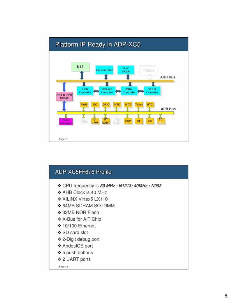
Platform IP Ready in ADP-XC5Platform IP Ready in ADP-XC5
N12N12Bus Controller
Bus Controller MAC
10/100
MAC
10/100 USB2.0USB2.0
LCD
Controller
LCD
ControllerSDRAM
Controller
SDRAM
ControllerDMA
Controller
DMA
ControllerSRAM
Controller
SRAM
Controller
AHB to APBBridge
AHB to APBBridge
PWMPWM I2CI2C GPIOGPIO INTCINTC WDTWDT TimerTimer RTCRTC
IrDAIrDA STUART
STUART
BT
UART
BT
UARTFF
UART
FF
UART SSPSSP CFCF I2SI2S SD/
MMC
SD/
MMCPower
Manager
Power
Manager
AHB Bus
APB Bus
Page 12
ADP-XC5FF676 ProfileADP-XC5FF676 Profile
� CPU frequency is 80 MHz : N1213; 40MHz : N903
� AHB Clock is 40 MHz
� XILINX Virtex5 LX110
� 64MB SDRAM SO-DIMM
� 32MB NOR Flash
� X-Bus for AIT Chip
� 10/100 Ethernet
� SD card slot
� 2-Digit debug port
� AndesICE port
� 5 push bottons
� 2 UART ports
7
Page 13
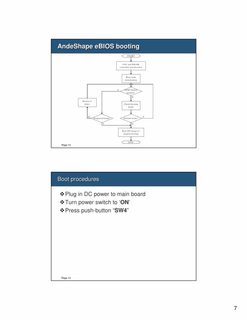
C P U an d D R A M
co n tro lle r in itia liz a tio n
G P IO b u tto n
p u sh ed ?
Y
N
S TA R T
C h eck b o o tin g
m o d e
B o o t co d e
in itia liza tio n
B u rn in o r
d em o
D efau lt m o d e?
E N D
N
Y
B o o t O S im ag e o r
d iagn o s is /s e tu p
D iag n o sis /se tu p ?
Y
N
AndeShape eBIOS bootingAndeShape eBIOS booting
Page 14
Boot procedures Boot procedures
�Plug in DC power to main board
�Turn power switch to ‘ON’
�Press push-button “SW4”
8
Page 15
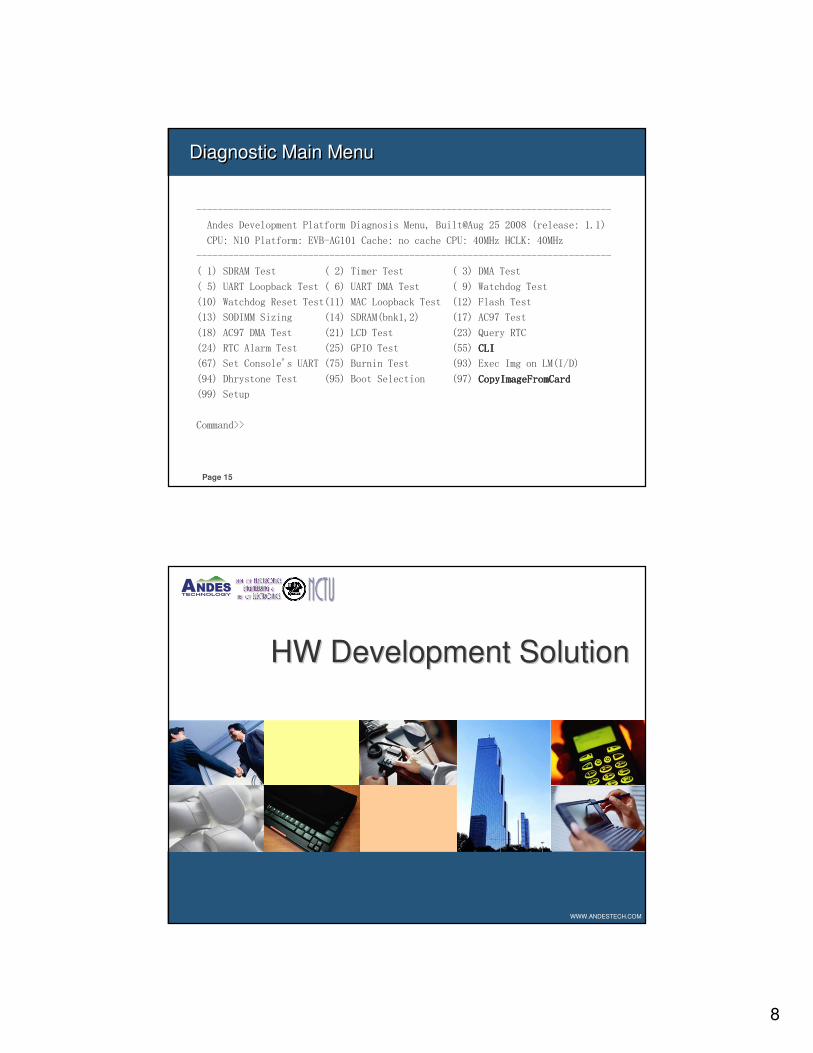
Diagnostic Main MenuDiagnostic Main Menu
------------------------------------------------------------------------------
Andes Development Platform Diagnosis Menu, Built@Aug 25 2008 (release: 1.1)
CPU: N10 Platform: EVB-AG101 Cache: no cache CPU: 40MHz HCLK: 40MHz
------------------------------------------------------------------------------
( 1) SDRAM Test ( 2) Timer Test ( 3) DMA Test
( 5) UART Loopback Test ( 6) UART DMA Test ( 9) Watchdog Test
(10) Watchdog Reset Test(11) MAC Loopback Test (12) Flash Test
(13) SODIMM Sizing (14) SDRAM(bnk1,2) (17) AC97 Test
(18) AC97 DMA Test (21) LCD Test (23) Query RTC
(24) RTC Alarm Test (25) GPIO Test (55) CLICLICLICLI
(67) Set Console's UART (75) Burnin Test (93) Exec Img on LM(I/D)
(94) Dhrystone Test (95) Boot Selection (97) CopyImageFromCardCopyImageFromCardCopyImageFromCardCopyImageFromCard
(99) Setup
Command>>
WWW.ANDESTECH.COM
HW Development SolutionHW Development SolutionHW Development Solution
9
Page 17
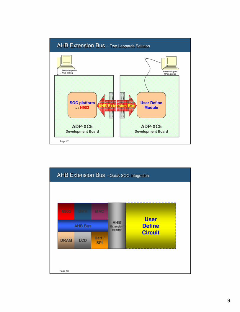
AHB Extension Bus – Two Leopards SolutionAHB Extension Bus – Two Leopards Solution
SOC platform
with N903
ADP-XC5Development Board
ADP-XC5Development Board
User Define
ModuleAHB Extension Bus
. SW development
. AICE debugDownload your FPGA design
Page 18
AHB Extension Bus – Quick SOC IntegrationAHB Extension Bus – Quick SOC Integration
UserDefineCircuit
AHBExtension
Header
N903
DRAM
DMA
LCD
MAC
Uart /
SPI
AHB Bus
10
Page 19
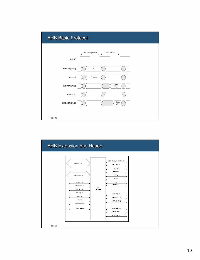
AHB Basic ProtocolAHB Basic Protocol
Page 20
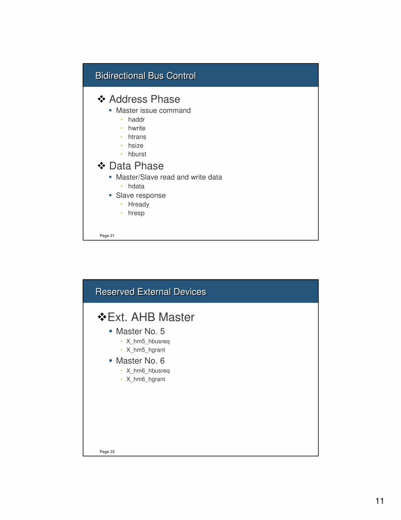
AHB Extension Bus HeaderAHB Extension Bus Header
11
Page 21
Bidirectional Bus ControlBidirectional Bus Control
� Address Phase� Master issue command
• haddr
• hwrite
• htrans
• hsize
• hburst
� Data Phase� Master/Slave read and write data
• hdata
� Slave response
• Hready
• hresp
Page 22
Reserved External DevicesReserved External Devices
�Ext. AHB Master� Master No. 5
• X_hm5_hbusreq
• X_hm5_hgrant
� Master No. 6 • X_hm6_hbusreq
• X_hm6_hgrant
12
Page 23
Reserved External DeviceReserved External Device
�Ext. AHB Slave� Slave No. 13,15,17,18,19,21,22
• X_hs13_hsel, X_hs15_hsel, X_hs17_hsel,
X_hs18_hsel, X_hs19_hsel, X_hs21_hsel,
X_hs22_hsel
• Memory Size : 1MB, 1MB, 1MB,
1MB, 1MB, 256MB,
128MB,
• Address Map : 0x90A0_0000, 0x90C0_0000, 0x90E0_0000,
0x90F0_0000, 0x9200_0000, 0xA000_0000,
0xB000_0000
Page 24
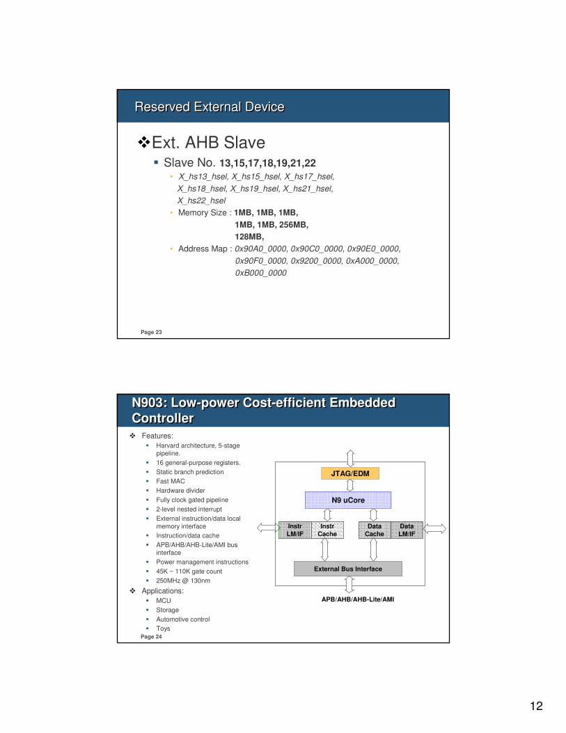
N903: Low-power Cost-efficient Embedded Controller
N903: Low-power Cost-efficient Embedded Controller
� Features:
� Harvard architecture, 5-stage
pipeline.
� 16 general-purpose registers.
� Static branch prediction
� Fast MAC
� Hardware divider
� Fully clock gated pipeline
� 2-level nested interrupt
� External instruction/data local
memory interface
� Instruction/data cache
� APB/AHB/AHB-Lite/AMI bus
interface
� Power management instructions
� 45K ~ 110K gate count
� 250MHz @ 130nm
� Applications:
� MCU
� Storage
� Automotive control
� Toys
External Bus Interface
APB/AHB/AHB-Lite/AMI
Instr
Cache
Instr
LM/IF
Data
Cache
Data
LM/IF
N9 uCore
JTAG/EDM
13
Page 25
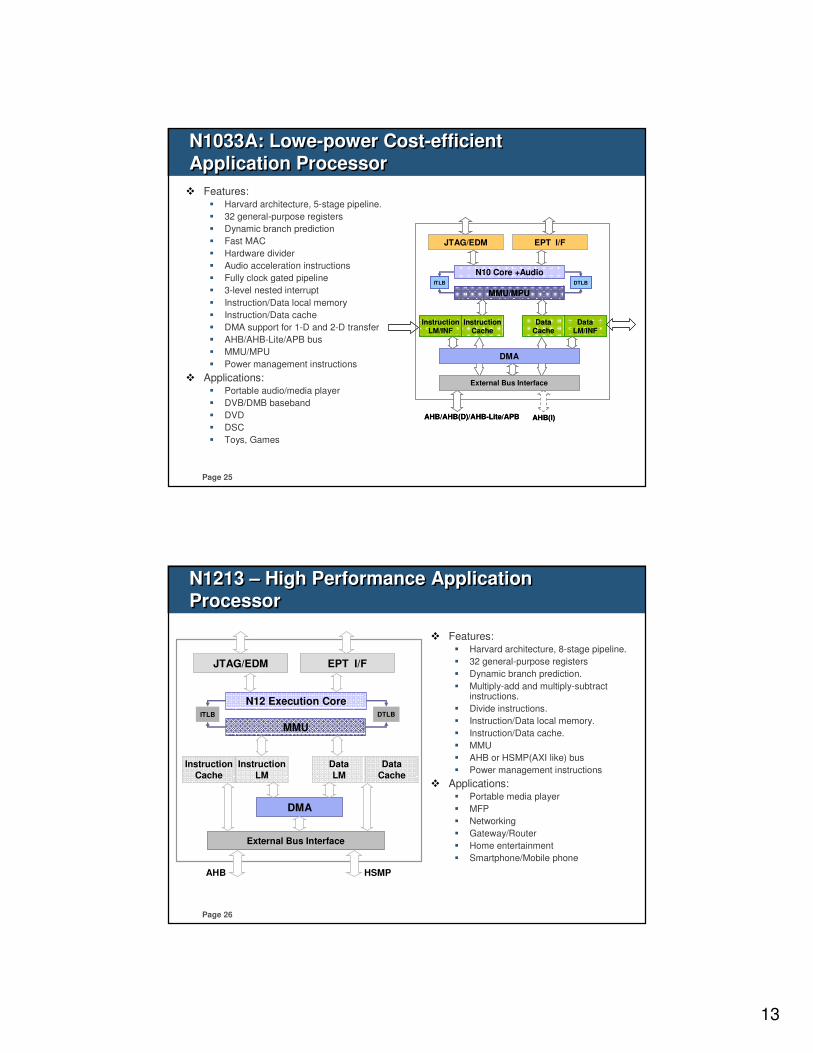
N1033A: Lowe-power Cost-efficient Application Processor
N1033A: Lowe-power Cost-efficient Application Processor
External Bus Interface
AHB/AHB(D)/AHB-Lite/APB
InstructionCache
InstructionLM/INF
DataCache
DataLM/INF
MMU/MPU
N10 Core +Audio
JTAG/EDM EPT I/F
DTLBITLB
DMA
AHB(I)
External Bus Interface
AHB/AHB(D)/AHB-Lite/APB
InstructionCache
InstructionLM/INF
DataCache
DataLM/INF
MMU/MPU
N10 Core +Audio
JTAG/EDM EPT I/F
DTLBITLB
DMA
AHB(I)
� Features:� Harvard architecture, 5-stage pipeline.
� 32 general-purpose registers
� Dynamic branch prediction
� Fast MAC
� Hardware divider
� Audio acceleration instructions
� Fully clock gated pipeline
� 3-level nested interrupt
� Instruction/Data local memory
� Instruction/Data cache
� DMA support for 1-D and 2-D transfer
� AHB/AHB-Lite/APB bus
� MMU/MPU
� Power management instructions
� Applications:� Portable audio/media player
� DVB/DMB baseband
� DVD
� DSC
� Toys, Games
Page 26
N1213 – High Performance Application Processor
N1213 – High Performance Application Processor
External Bus Interface
AHB
Instruction
LM
Instruction
Cache
Data
LM
Data
Cache
MMU
N12 Execution Core
JTAG/EDM EPT I/F
DTLBITLB
HSMP
DMA
� Features:� Harvard architecture, 8-stage pipeline.
� 32 general-purpose registers
� Dynamic branch prediction.
� Multiply-add and multiply-subtract instructions.
� Divide instructions.
� Instruction/Data local memory.
� Instruction/Data cache.
� MMU
� AHB or HSMP(AXI like) bus
� Power management instructions
� Applications:� Portable media player
� MFP
� Networking
� Gateway/Router
� Home entertainment
� Smartphone/Mobile phone
14
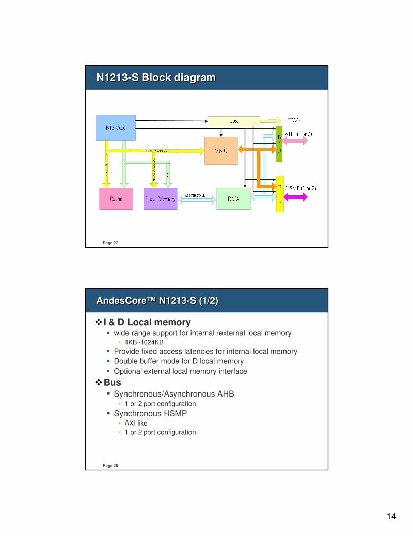
Page 27
N1213-S Block diagramN1213-S Block diagram
Page 28
AndesCore™ N1213-S (1/2)AndesCore™ N1213-S (1/2)
�I & D Local memory� wide range support for internal /external local memory
• 4KB~1024KB
� Provide fixed access latencies for internal local memory
� Double buffer mode for D local memory
� Optional external local memory interface
�Bus� Synchronous/Asynchronous AHB
• 1 or 2 port configuration
� Synchronous HSMP • AXI like
• 1 or 2 port configuration
15
Page 29
AndesCore™ N1213-S (2/2)AndesCore™ N1213-S (2/2)
� For performance� Improved memory accesses:
• 1D/2D DMA, load/store multiple
� Efficient synchronization without locking the whole bus• Load lock, store conditional instructions
� Vectored interrupt to improve real-time performance• 6 interrupt signals
� MMU• Optional HW page table walker• TLB management instructions
� For flexibility� Memory-mapped IO space
� JTAG-based debug support
� Optional embedded program trace interface
� Performance monitors for performance tuning
� Bi-endian modes to support flexible data input
Page 30
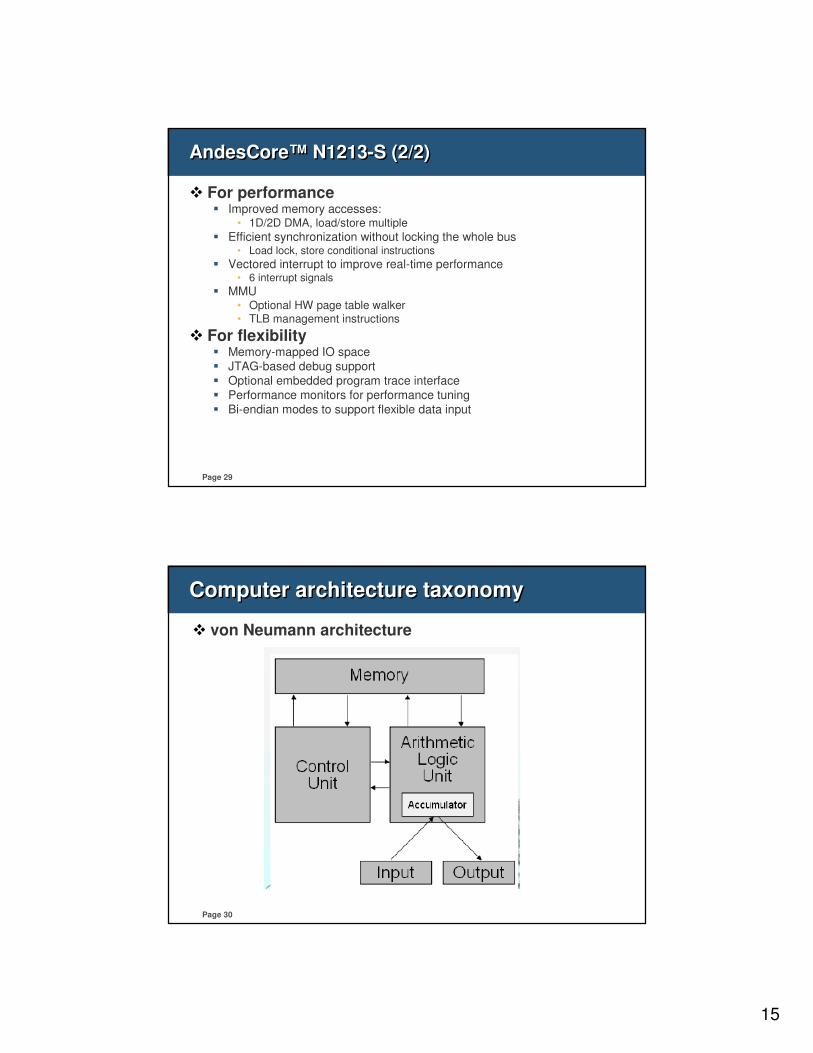
Computer architecture taxonomyComputer architecture taxonomy
� von Neumann architecture
16
Page 31
Computer architecture taxonomy (1/3)Computer architecture taxonomy (1/3)
� von Neumann architecture� Features of each:
• Execution in multiple cycles
� Serial fetch instructions & data
� Single memory structure• Can get data/program mixed
• Data/instructions same size
� Examples, von Neumann: PCs (Intel 80x86/Pentium, Motorola 68000, Mot 68xx uC families
Page 32
Computer architecture taxonomy (2/3)Computer architecture taxonomy (2/3)
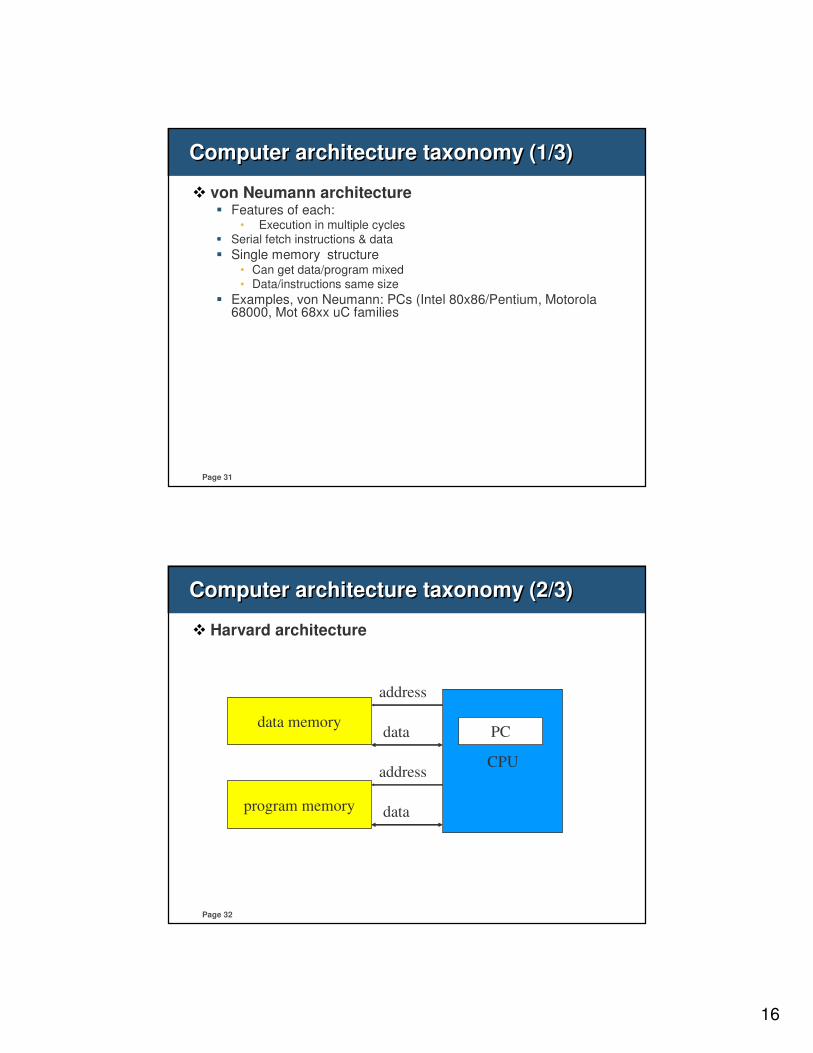
� Harvard architecture
CPU
PCdata memory
program memory
address
data
address
data

17
Page 33
Computer architecture taxonomy (3/3)Computer architecture taxonomy (3/3)
� Harvard architecture� Features of each: Execution in 1 cycle� Parallel fetch instructions & data
� More Complex H/W• Instructions and data always separate
• Different code/data path widths (E.G. 14 bit instructions, 8 bit data)
� Harvard: 8051, Microchip PIC families, Atmel AVR, AndeScore
Page 34
Architectures: CISC vs. RISC (1/2)Architectures: CISC vs. RISC (1/2)
�CISC - Complex Instruction Set Computers:� Emphasis on hardware
� Includes multi-clock complex instructions
� Memory-to-memory
� Sophisticated arithmetic (multiply, divide, trigonometry etc.).
� Special instructions are added to optimize performance with particular compilers.
18
Page 35
Architectures: CISC vs. RISC (2/2)Architectures: CISC vs. RISC (2/2)
�RISC - Reduced Instruction Set Computers:� A very small set of primitive instructions� Fixed instruction format
� Emphasis on software
� All instructions execute in one cycle (Fast!).
� Register to register (except Load/Store instructions)
� Pipline architecture
Page 36
CISC, RISC, MISC, etcCISC, RISC, MISC, etc
�CISC: complex instruction set computer
� Intel’s x86 and Motorola’s 68*
�RISC: reduced instruction set computer
� Load/store architecture
� (Mostly) single-cycle instructions
• Divide can’t be in 1 cycle
• Not to mention floating-point operations
�MISC: mixed instruction set computer
� Andes/ARM: load/store multiple (addresses)
• A little richer in semantics, but very regular in main pipeline.
� SIMD instructions: rich in semantics, but regular
� Complex coprocessor instructions
• Coprocessor can be a little more complicated since it’s separate from
main pipeline.
19
Page 37
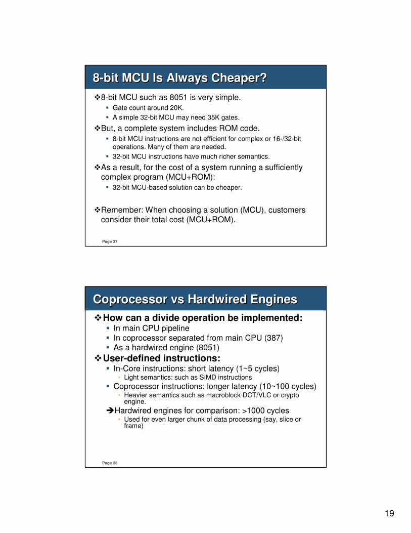
8-bit MCU Is Always Cheaper?8-bit MCU Is Always Cheaper?
�8-bit MCU such as 8051 is very simple.
� Gate count around 20K.
� A simple 32-bit MCU may need 35K gates.
�But, a complete system includes ROM code.
� 8-bit MCU instructions are not efficient for complex or 16-/32-bit
operations. Many of them are needed.
� 32-bit MCU instructions have much richer semantics.
�As a result, for the cost of a system running a sufficiently complex program (MCU+ROM):
� 32-bit MCU-based solution can be cheaper.
�Remember: When choosing a solution (MCU), customers consider their total cost (MCU+ROM).
Page 38
Coprocessor vs Hardwired EnginesCoprocessor vs Hardwired Engines
�How can a divide operation be implemented:� In main CPU pipeline
� In coprocessor separated from main CPU (387)� As a hardwired engine (8051)
�User-defined instructions:� In-Core instructions: short latency (1~5 cycles)
• Light semantics: such as SIMD instructions
� Coprocessor instructions: longer latency (10~100 cycles)• Heavier semantics such as macroblock DCT/VLC or crypto
engine.
�Hardwired engines for comparison: >1000 cycles• Used for even larger chunk of data processing (say, slice or
frame)
20
Page 39
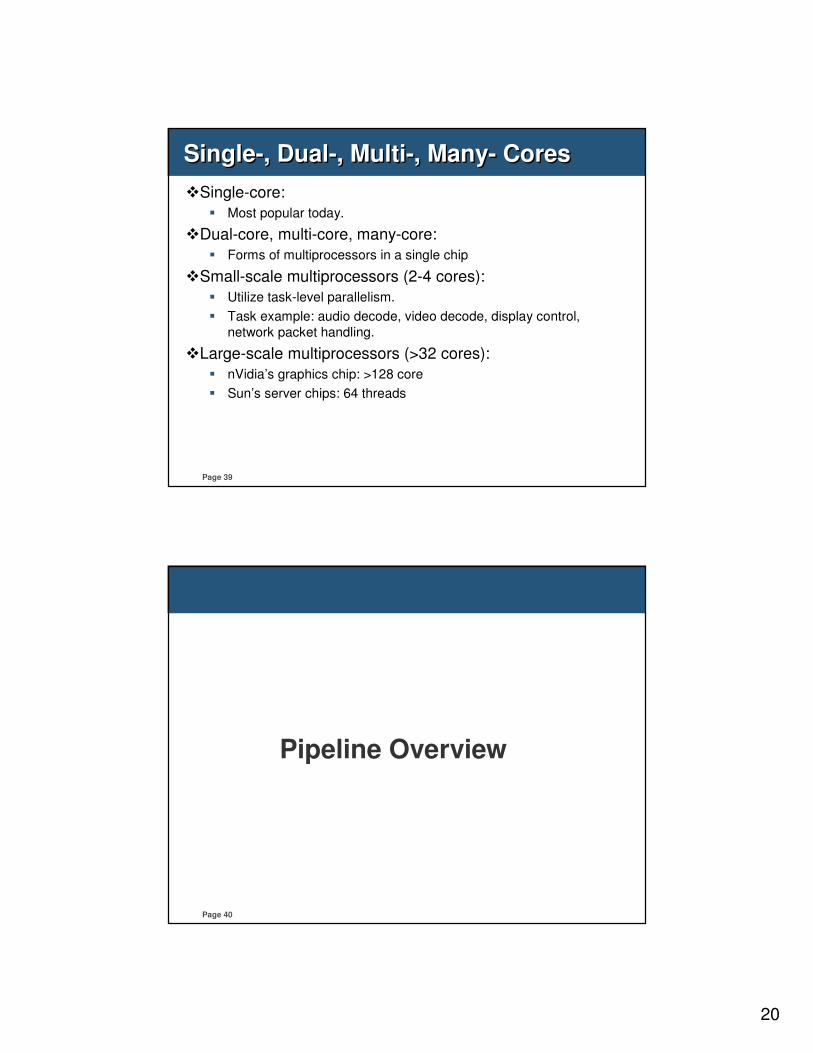
Single-, Dual-, Multi-, Many- CoresSingle-, Dual-, Multi-, Many- Cores
�Single-core:
� Most popular today.
�Dual-core, multi-core, many-core:
� Forms of multiprocessors in a single chip
�Small-scale multiprocessors (2-4 cores):
� Utilize task-level parallelism.
� Task example: audio decode, video decode, display control,
network packet handling.
�Large-scale multiprocessors (>32 cores):
� nVidia’s graphics chip: >128 core
� Sun’s server chips: 64 threads
Page 40
Pipeline Overview
21
Page 41
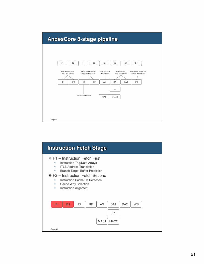
AndesCore 8-stage pipelineAndesCore 8-stage pipeline
RF
EX
IF1 IF2 ID DA1 DA2 WB
Instruction-Fetch
First and Second
Instruction Decode
Instruction Issue and
Register File Read
AG
Instruction Retire and
Result Write Back
Data Access
First and Second
Data Address
Generation
F1 F2 I1 I2 E1 E2 E3 E4
MAC1 MAC2
Page 42
Instruction Fetch StageInstruction Fetch Stage
� F1 – Instruction Fetch First� Instruction Tag/Data Arrays
� ITLB Address Translation
� Branch Target Buffer Prediction
� F2 – Instruction Fetch Second� Instruction Cache Hit Detection
� Cache Way Selection
� Instruction Alignment
IF1 IF2 ID RF AG DA1 DA2 WB
EX
MAC1 MAC2
22
Page 43
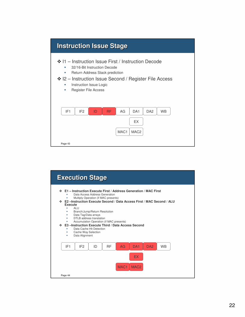
Instruction Issue StageInstruction Issue Stage
� I1 – Instruction Issue First / Instruction Decode� 32/16-Bit Instruction Decode
� Return Address Stack prediction
� I2 – Instruction Issue Second / Register File Access� Instruction Issue Logic
� Register File Access
IF1 IF2 ID RF AG DA1 DA2 WB
EX
MAC1 MAC2
Page 44
Execution StageExecution Stage
� E1 – Instruction Execute First / Address Generation / MAC First� Data Access Address Generation
� Multiply Operation (if MAC presents)
� E2 –Instruction Execute Second / Data Access First / MAC Second / ALU Execute� ALU
� Branch/Jump/Return Resolution
� Data Tag/Data arrays
� DTLB address translation� Accumulation Operation (if MAC presents)
� E3 –Instruction Execute Third / Data Access Second� Data Cache Hit Detection
� Cache Way Selection
� Data Alignment
IF1 IF2 ID RF AG DA1 DA2 WB
EX
MAC1 MAC2
23
Page 45
Write Back StageWrite Back Stage
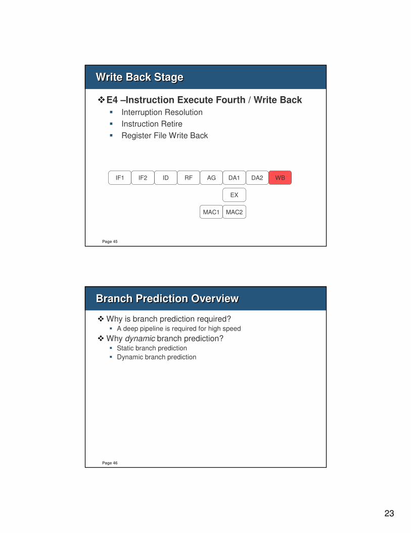
�E4 –Instruction Execute Fourth / Write Back
� Interruption Resolution
� Instruction Retire
� Register File Write Back
IF1 IF2 ID RF AG DA1 DA2 WB
EX
MAC1 MAC2
Page 46
Branch Prediction OverviewBranch Prediction Overview
� Why is branch prediction required?� A deep pipeline is required for high speed
� Why dynamic branch prediction?� Static branch prediction
� Dynamic branch prediction
24
Page 47
Branch Prediction UnitBranch Prediction Unit
�Branch Target Buffer (BTB)� 128 entries of 2-bit saturating counters
� 128 entries, 32-bit predicted PC and 26-bit address tag
�Return Address Stack (RAS)
� Four entries
�BTB and RAS updated by committing branches/jumps
Page 48
BTB Instruction PredictionBTB Instruction Prediction
� BTB predictions are performed based on the previous PC instead of the actual instruction decoding information, BTB may make the following two mistakes� Wrongly predicts the non-branch/jump instructions as branch/jump
instructions
� Wrongly predicts the instruction boundary (32-bit -> 16-bit)
� If these cases are detected, IFU will trigger a BTB instruction misprediction in the I1 stage and re-start the program sequence from the recovered PC. There will be a 2-cycle penalty introduced here
F1 F2 I1
F1 F2
F1
branch
PC+4
PC+4
BTB instruction misprediction
F1 F2 I1
killed
killed
Recovered PC
25
Page 49
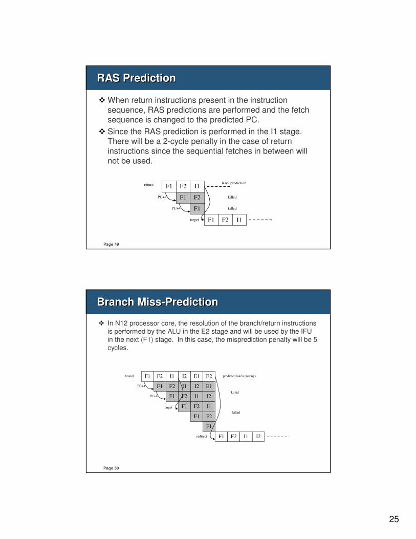
RAS PredictionRAS Prediction
� When return instructions present in the instruction
sequence, RAS predictions are performed and the fetch
sequence is changed to the predicted PC.
� Since the RAS prediction is performed in the I1 stage. There will be a 2-cycle penalty in the case of return
instructions since the sequential fetches in between will
not be used.
F1 F2 I1
F1 F2
F1
return
PC+4
PC+4
RAS prediction
F1 F2 I1
killed
killed
target
Page 50
Branch Miss-PredictionBranch Miss-Prediction
� In N12 processor core, the resolution of the branch/return instructions
is performed by the ALU in the E2 stage and will be used by the IFU
in the next (F1) stage. In this case, the misprediction penalty will be 5
cycles.
F1 F2 I1 I2
F1 F2 I1 I2
F1 F2 I1 I2
PC+4
PC+4
F1 F2 I1
F1 F2
E1 E2
E1
branch
target
F1
F1 F2 I1 I2
predicted taken (wrong)
killed
killed
redirect
26
Page 51
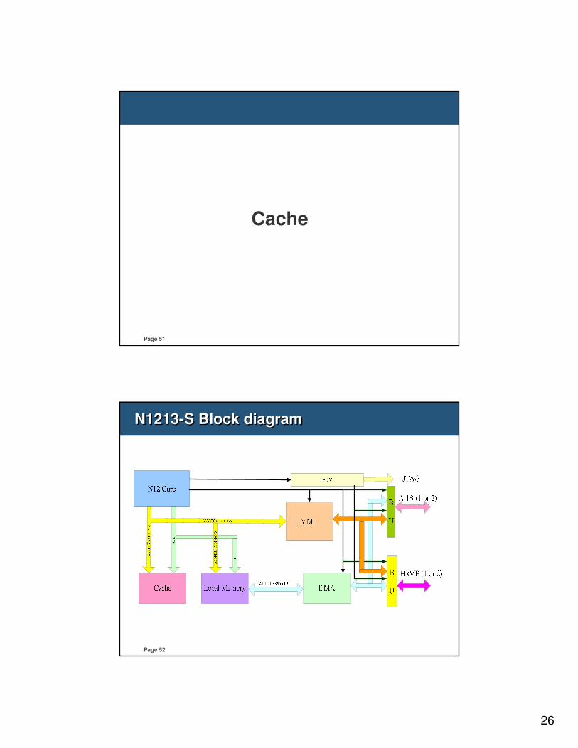
Cache
Page 52
N1213-S Block diagramN1213-S Block diagram
27
Page 53
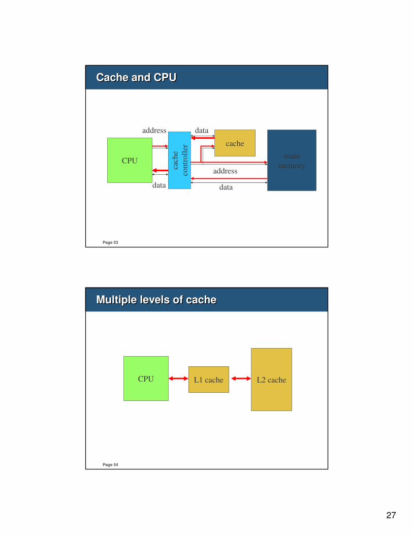
Cache and CPUCache and CPU
CPU
cach
e
contr
oll
er
cache
main
memory
data
data
address
data
address
Page 54
Multiple levels of cacheMultiple levels of cache
CPU L1 cache L2 cache
28
Page 55
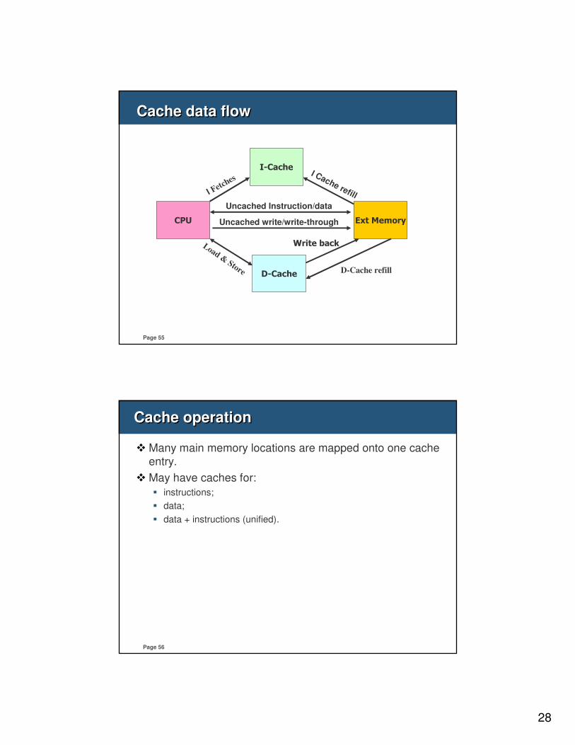
Cache data flowCache data flow
I-Cache
D-Cache
CPU Ext Memory
I Fetc
hes
Load &
Store
I Cache refill
Uncached Instruction/data
Uncached write/write-through
Write back
D-Cache refill
Page 56
Cache operationCache operation
� Many main memory locations are mapped onto one cache
entry.
� May have caches for:
� instructions;
� data;
� data + instructions (unified).

29
Page 57
Replacement policyReplacement policy
� Replacement policy: strategy for choosing which cache
entry to throw out to make room for a new memory
location.
� Two popular strategies:
� Random.
� Least-recently used (LRU).
Page 58
Write operationsWrite operations
� Write-through: immediately copy write to main memory.
� Write-back: write to main memory only when location is
removed from cache.
30
Page 59
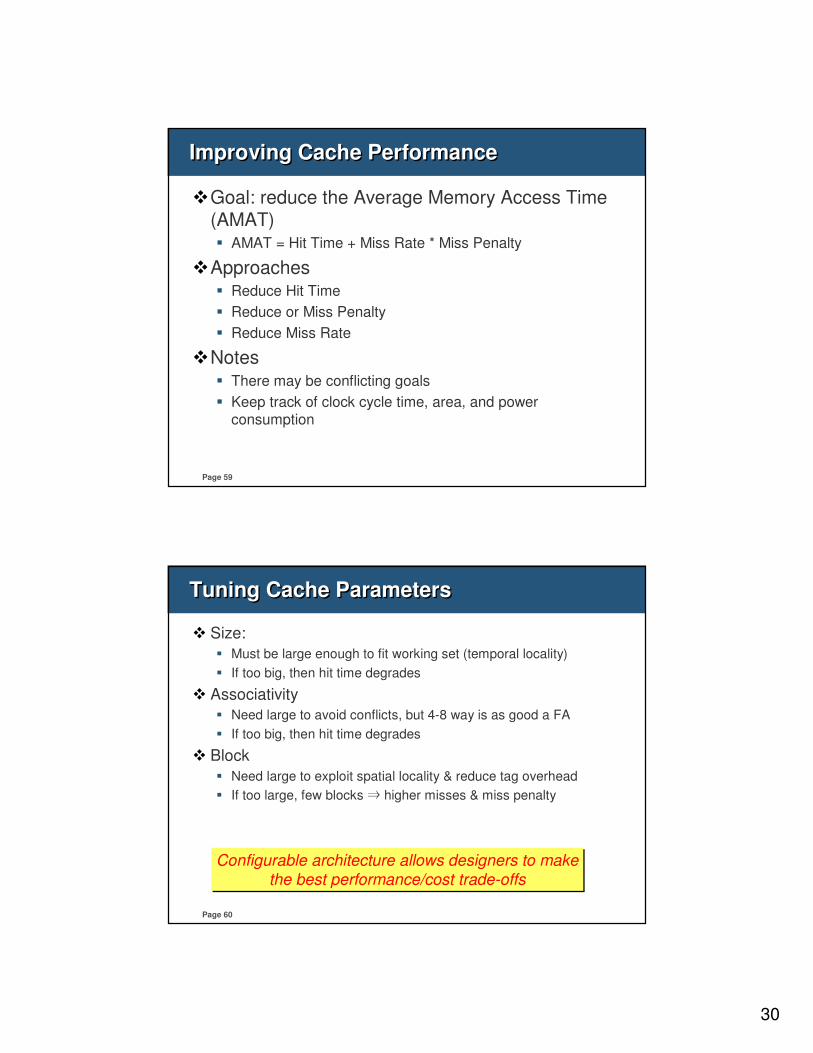
Improving Cache PerformanceImproving Cache Performance
�Goal: reduce the Average Memory Access Time (AMAT)� AMAT = Hit Time + Miss Rate * Miss Penalty
�Approaches� Reduce Hit Time
� Reduce or Miss Penalty
� Reduce Miss Rate
�Notes� There may be conflicting goals
� Keep track of clock cycle time, area, and power consumption
Page 60
Tuning Cache ParametersTuning Cache Parameters
� Size:
� Must be large enough to fit working set (temporal locality)
� If too big, then hit time degrades
� Associativity
� Need large to avoid conflicts, but 4-8 way is as good a FA
� If too big, then hit time degrades
� Block
� Need large to exploit spatial locality & reduce tag overhead
� If too large, few blocks ⇒ higher misses & miss penalty
Configurable architecture allows designers to make
the best performance/cost trade-offs
Configurable architecture allows designers to make
the best performance/cost trade-offs
31
Page 61
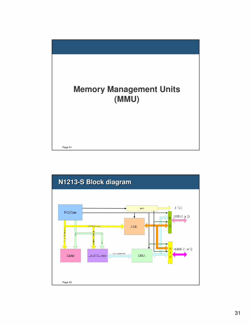
Memory Management Units(MMU)
Page 62
N1213-S Block diagramN1213-S Block diagram
32
Page 63
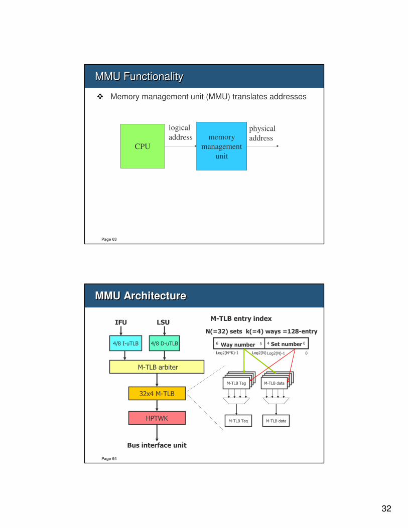
MMU FunctionalityMMU Functionality
� Memory management unit (MMU) translates addresses
CPU
memory
management
unit
logical
addressphysical
address
Page 64
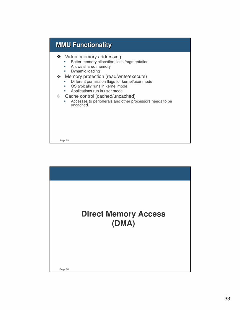
MMU ArchitectureMMU Architecture
4/8 I-uTLB 4/8 D-uTLB
M-TLB arbiter
32x4 M-TLB
HPTWK
N(=32) sets k(=4) ways =128-entry
M-TLB entry index
Set numberWay number
Log2(N)-1 0Log2(N*K)-1 Log2(N)
4 056
Bus interface unit
IFU LSU
M-TLB Tag
M-TLB Tag
M-TLB data
M-TLB data
33
Page 65
MMU FunctionalityMMU Functionality
� Virtual memory addressing� Better memory allocation, less fragmentation
� Allows shared memory
� Dynamic loading
� Memory protection (read/write/execute)� Different permission flags for kernel/user mode
� OS typically runs in kernel mode
� Applications run in user mode
� Cache control (cached/uncached)� Accesses to peripherals and other processors needs to be
uncached.
Page 66
Direct Memory Access(DMA)
34
Page 67
N1213-S Block diagramN1213-S Block diagram
Page 68
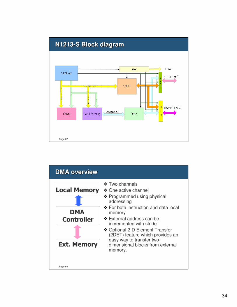
DMA overviewDMA overview
DMA Controller
Local Memory
Ext. Memory
� Two channels
� One active channel
� Programmed using physical addressing
� For both instruction and data local memory
� External address can be incremented with stride
� Optional 2-D Element Transfer (2DET) feature which provides an easy way to transfer two-dimensional blocks from external memory.
35
Page 69
Width byte stride (in DMA Setup register)=1
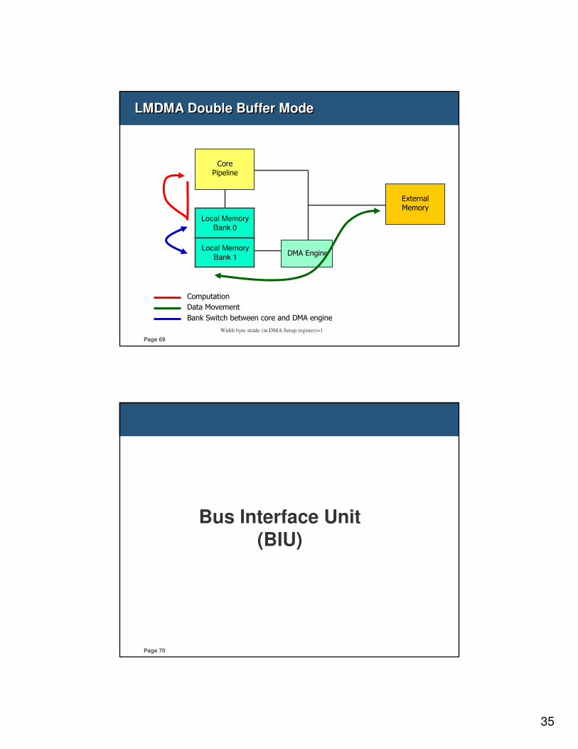
LMDMA Double Buffer ModeLMDMA Double Buffer Mode
Local Memory
Bank 0
Local Memory
Bank 1DMA Engine
CorePipeline
ExternalMemory
Computation
Data Movement
Bank Switch between core and DMA engine
Page 70
Bus Interface Unit (BIU)
36
Page 71
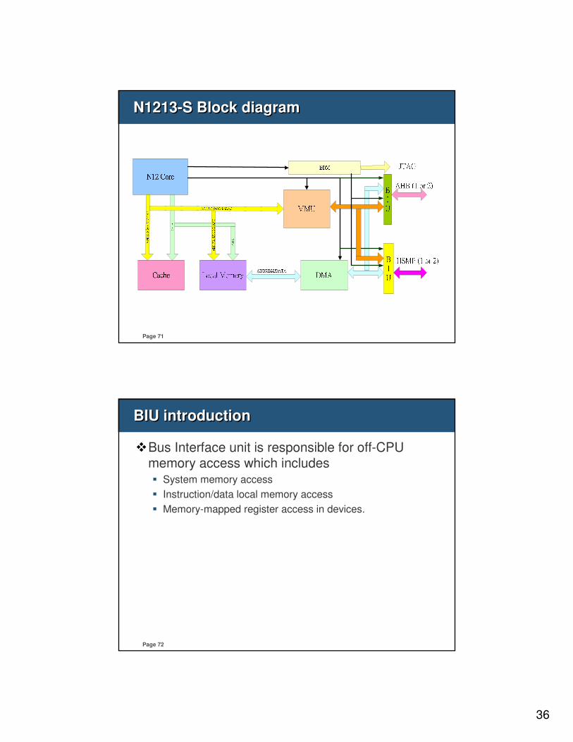
N1213-S Block diagramN1213-S Block diagram
Page 72
BIU introductionBIU introduction
�Bus Interface unit is responsible for off-CPU memory access which includes � System memory access
� Instruction/data local memory access
� Memory-mapped register access in devices.
37
Page 73
�Compliance to AHB/AHB-Lite/APB
�High Speed Memory Port
�Andes Memory Interface
�External LM Interface
Bus InterfaceBus Interface
Page 74
HSMP – High speed memory portHSMP – High speed memory port
�N12 also provides a high speed memory port interface which has higher bus protocol efficiency and can run at a higher frequency to connect to a memory controller.
�The high speed memory port will be AMBA3.0
(AXI) protocol compliant, but with reduced I/O requirements.
38
WWW.ANDESTECH.COM
Thank YouThank You