Analysis of RF Front-End Non-linearity on Symbol Error ...M-PSK modulation schemes. For high blocker...
89
Analysis of RF Front-End Non-linearity on Symbol Error Rate in the Presence of M-PSK Blocking Signals Jennifer Dsouza Thesis submitted to the Faculty of the Virginia Polytechnic Institute and State University in partial fulfillment of the requirements for the degree of Master of Science in Electrical Engineering Vuk Marojevic, Chair Jeffrey H. Reed R. Michael Buehrer July 19, 2017 Blacksburg, Virginia Keywords: Non-linearity, Bit error rate, Symbol error rate, M-PSK modulation, Blocking Signals Copyright 2017, Jennifer Dsouza
Transcript of Analysis of RF Front-End Non-linearity on Symbol Error ...M-PSK modulation schemes. For high blocker...
Analysis of RF Front-End Non-linearity on SymbolError Rate in the Presence of M-PSK Blocking Signals
Jennifer Dsouza
Thesis submitted to the Faculty of theVirginia Polytechnic Institute and State University
in partial fulfillment of the requirements for the degree of
Master of Sciencein
Electrical Engineering
Vuk Marojevic, ChairJeffrey H. Reed
R. Michael Buehrer
July 19, 2017Blacksburg, Virginia
Keywords: Non-linearity, Bit error rate, Symbol error rate, M-PSK modulation, BlockingSignals
Copyright 2017, Jennifer Dsouza
Analysis of RF Front-End Non-linearity on Symbol Error Rate inthe Presence of M-PSK Blocking Signals
Jennifer Dsouza
ACADEMIC ABSTRACT
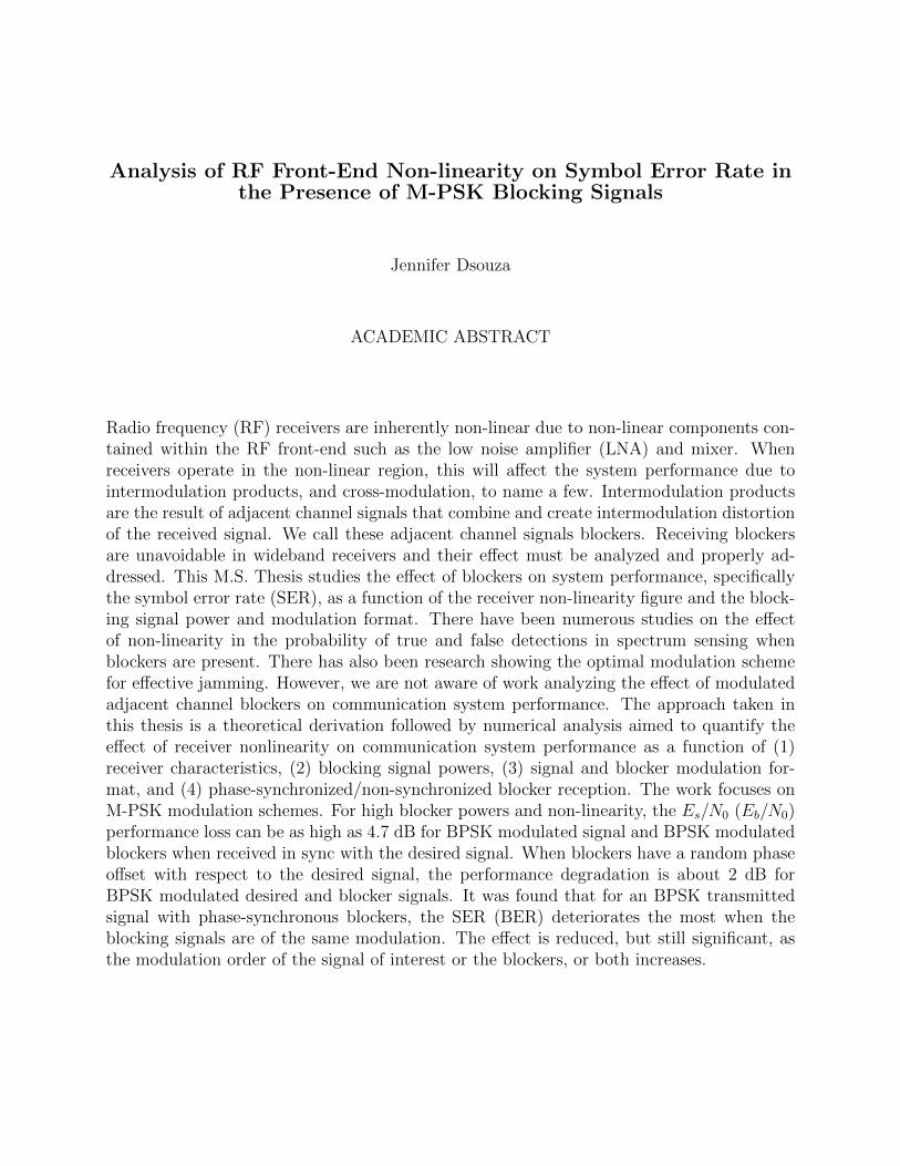
Radio frequency (RF) receivers are inherently non-linear due to non-linear components con-tained within the RF front-end such as the low noise amplifier (LNA) and mixer. Whenreceivers operate in the non-linear region, this will affect the system performance due tointermodulation products, and cross-modulation, to name a few. Intermodulation productsare the result of adjacent channel signals that combine and create intermodulation distortionof the received signal. We call these adjacent channel signals blockers. Receiving blockersare unavoidable in wideband receivers and their effect must be analyzed and properly ad-dressed. This M.S. Thesis studies the effect of blockers on system performance, specificallythe symbol error rate (SER), as a function of the receiver non-linearity figure and the block-ing signal power and modulation format. There have been numerous studies on the effectof non-linearity in the probability of true and false detections in spectrum sensing whenblockers are present. There has also been research showing the optimal modulation schemefor effective jamming. However, we are not aware of work analyzing the effect of modulatedadjacent channel blockers on communication system performance. The approach taken inthis thesis is a theoretical derivation followed by numerical analysis aimed to quantify theeffect of receiver nonlinearity on communication system performance as a function of (1)receiver characteristics, (2) blocking signal powers, (3) signal and blocker modulation for-mat, and (4) phase-synchronized/non-synchronized blocker reception. The work focuses onM-PSK modulation schemes. For high blocker powers and non-linearity, the Es/N0 (Eb/N0)performance loss can be as high as 4.7 dB for BPSK modulated signal and BPSK modulatedblockers when received in sync with the desired signal. When blockers have a random phaseoffset with respect to the desired signal, the performance degradation is about 2 dB forBPSK modulated desired and blocker signals. It was found that for an BPSK transmittedsignal with phase-synchronous blockers, the SER (BER) deteriorates the most when theblocking signals are of the same modulation. The effect is reduced, but still significant, asthe modulation order of the signal of interest or the blockers, or both increases.

Analysis of RF Front-End Non-linearity on Symbol Error Rate inthe Presence of M-PSK Blocking Signals
Jennifer Dsouza
GENERAL AUDIENCE ABSTRACT
This thesis analyzes the effect of non-linear components in wireless receivers on communica-tion system performance. We consider that two strong radio frequency signals adjacent infrequency to the desired signal enter the receiver and cause signal distortion known as 3rdorder intermodulation distortion. We analyze the effect on the symbol error rate (SER) inthe presence of two modulated blockers. SER defines the ratio of erroneously detected sym-bols to the total number of transmitted symbols and is a function of the modulation schemeand radio channel conditions. The SER analysis is done for Phase Shift Keying (PSK) mod-ulated signals and blockers for different receiver types and blocker power levels. This thesisderives the theoretical SER expressions followed by numerical analysis aimed to quantifythe effect of receiver non-linearity on communication system performance as a function of(1) receiver characteristics, (2) blocking signal powers, (3) signal and blocker modulationformats, and (4) phase-synchronized/non-synchronized reception of blockers. We justify theneed for these new SER expressions and verify them via simulations. The thesis showsthat modulated blockers can significantly impact communication system performance if theblockers are strong with respect to the signal of interest and if the device is highly non-linear.The work also shows that the performance degradation is a function of the blocker signalcharacteristics, but there are ways to overcome this loss by design or management. This hasimportant implications on the management of spectrum in the new shared spectrum bands,where heterogeneous systems and devices will coexist with strong signals coming from nearbytransmitters, radars or TV stations, among others.

Dedication
To my parents (Mary Thomas and William D’Souza) and my brother (Geoffrey D’Souza).
iv

Acknowledgements
First off, I would like to sincerely thank Dr. Vuk Marojevic for guiding me throughout myThesis. Every input was invaluable and immensely appreciated. Thank you for the countlesssleepless nights that you put into making the completion of this Thesis possible.
I would also like to thank my committee members, Dr. Jeffrey H. Reed and Dr. R. MichaelBuehrer for their support and insights into the work.
Thank you Aditya Padaki for always rescuing me when I was stuck in my work, pointing metowards the right resources and explaining concepts repeatedly, with patience.
A huge thanks to my Mom, who has always believed in me and never let me give up. Thankyou for the support and encouragement in my most difficult times.
Lastly, I would like to thank all my friends at Virginia Tech. Iqtidar Ahmad Khan, thankyou for bearing all my rants and always supporting me every time I thought I couldn’t makeit. Thank you Aishwarya Sukesh Kumar, Disha Sardana, Tarun Cousik and Komalbir Kaurfor the being the best friends I could have at VT. Without you Graduate School would havebeen more stressful than it was, and definitely boring!
v

Contents
Dedication iv
Acknowledgements v
1 Introduction 1
2 Memoryless Modulation Schemes 7
2.1 Fundamental Blocks of a Digital Communication System . . . . . . . . . . . 8
2.2 Types of Memoryless Modulation Schemes . . . . . . . . . . . . . . . . . . . 9
2.3 System Performance for Memoryless Modulation Schemes . . . . . . . . . . . 11
3 Signal Distortion due to Receiver RF Non-Linearity 15
3.1 Harmonic Distortion . . . . . . . . . . . . . . . . . . . . . . . . . . . . . . . 16
3.2 Gain Compression . . . . . . . . . . . . . . . . . . . . . . . . . . . . . . . . . 17
3.3 Cross Modulation . . . . . . . . . . . . . . . . . . . . . . . . . . . . . . . . . 19
3.4 Intermodulation . . . . . . . . . . . . . . . . . . . . . . . . . . . . . . . . . . 19
4 System Model and SER Derivations 23
4.1 System Model . . . . . . . . . . . . . . . . . . . . . . . . . . . . . . . . . . . 23
4.2 Assumptions . . . . . . . . . . . . . . . . . . . . . . . . . . . . . . . . . . . . 29
4.3 BER Analysis for BPSK . . . . . . . . . . . . . . . . . . . . . . . . . . . . . 29
vi
4.4 SER Analysis for M-PSK . . . . . . . . . . . . . . . . . . . . . . . . . . . . . 32
4.5 Non-Synchronous Reception of Blockers . . . . . . . . . . . . . . . . . . . . . 36
4.6 Union Bound and Improved Union Bound . . . . . . . . . . . . . . . . . . . 38
4.7 Limitations of the Model and Expressions . . . . . . . . . . . . . . . . . . . 40
4.7.1 Random Phase SER Curves . . . . . . . . . . . . . . . . . . . . . . . 41
4.7.2 Randomize Power of Blockers . . . . . . . . . . . . . . . . . . . . . . 41
4.7.3 Randomize Frequency . . . . . . . . . . . . . . . . . . . . . . . . . . 42
5 Numerical Results and Analyses 44
5.1 Power Calibration . . . . . . . . . . . . . . . . . . . . . . . . . . . . . . . . . 44
5.2 Simulator . . . . . . . . . . . . . . . . . . . . . . . . . . . . . . . . . . . . . 45
5.3 BER Analyses for BPSK Modulated Signal of Interest . . . . . . . . . . . . . 46
5.3.1 Numerical Analyses for MB-PSK and MC-PSK Modulated Blockerswith Fixed Blocker Power Levels (Phase-Synchronous Signals) . . . . 47
5.3.2 Mathematical Reasoning Behind Identical BER Performance for Cer-tain Modulation Orders of the Blockers . . . . . . . . . . . . . . . . . 48
5.3.3 Varying IIP3 and Blocker Power Levels . . . . . . . . . . . . . . . . 55
5.3.4 Varying Phase Offsets . . . . . . . . . . . . . . . . . . . . . . . . . . 57
5.4 SER Analysis for QPSK Modulated Signal of Interest . . . . . . . . . . . . 62
6 Conclusions and Future Work 68
Appendix A Conversion From Rectangular Coordinates to Polar Coordi-nates 71
Appendix B Integral Evaluation 73
Bibliography 74
vii
List of Figures
1.1 Spectrum of the blocking and desired signals . . . . . . . . . . . . . . . . . . 2
2.1 A simplified structure of a digital communication system. . . . . . . . . . . . 8
2.2 Amplitude Shift Keying for M = 2 (also known as on-off keying or OOK) . . 9
2.3 ASK/PAM constellation diagram for (a) M = 2, (b) M = 4 . . . . . . . . . . 10
2.4 Constellation for 3-FSK . . . . . . . . . . . . . . . . . . . . . . . . . . . . . 10
2.5 Constellation diagram for (a) M = 4, (b) M = 8 . . . . . . . . . . . . . . . . 11
2.6 Constellation for (a) circular 8-QAM (8 PAM-PSK), (b) rectangular 8-QAM,and 16-QAM . . . . . . . . . . . . . . . . . . . . . . . . . . . . . . . . . . . 12
2.7 SER plot for BPSK, QPSK, 8-PSK, and 16-PSK signaling. . . . . . . . . . . 14
2.8 BER plot for BPSK, QPSK, 8-PSK, and 16-PSK signaling. . . . . . . . . . . 14
3.1 A simplified structure of a digital communication system. The block in red isthe system under study - that is, the non-linear RF Front-End . . . . . . . . 15
3.2 Typical non-linear RF Front-End . . . . . . . . . . . . . . . . . . . . . . . . 16
3.3 Transfer function of a compressive amplifier on log scale . . . . . . . . . . . . 18
3.4 Illustration of the transfer of modulation due to the SOI from the interferer,due to non-linear devices . . . . . . . . . . . . . . . . . . . . . . . . . . . . . 19
3.5 Intermods closest to the fundamental signals formed due to receiver non-linearity at 2f1 − f2 and 2f2 − f1 . . . . . . . . . . . . . . . . . . . . . . . . 20
3.6 Graph depicting the theoretical IP3 point. Aout, ND Ain are essentially voltagevalues. . . . . . . . . . . . . . . . . . . . . . . . . . . . . . . . . . . . . . . . 21
viii
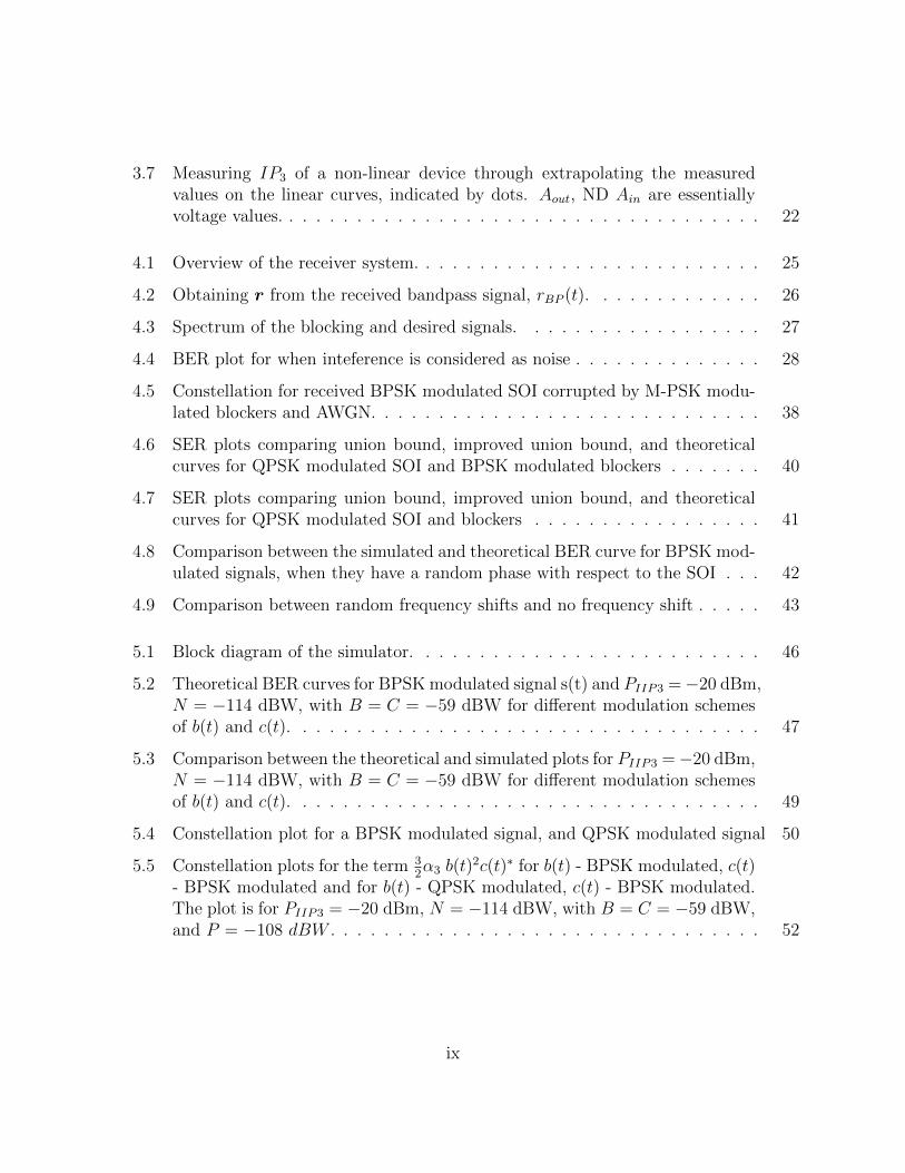
3.7 Measuring IP3 of a non-linear device through extrapolating the measuredvalues on the linear curves, indicated by dots. Aout, ND Ain are essentiallyvoltage values. . . . . . . . . . . . . . . . . . . . . . . . . . . . . . . . . . . . 22
4.1 Overview of the receiver system. . . . . . . . . . . . . . . . . . . . . . . . . . 25
4.2 Obtaining r from the received bandpass signal, rBP (t). . . . . . . . . . . . . 26
4.3 Spectrum of the blocking and desired signals. . . . . . . . . . . . . . . . . . 27
4.4 BER plot for when inteference is considered as noise . . . . . . . . . . . . . . 28
4.5 Constellation for received BPSK modulated SOI corrupted by M-PSK modu-lated blockers and AWGN. . . . . . . . . . . . . . . . . . . . . . . . . . . . . 38
4.6 SER plots comparing union bound, improved union bound, and theoreticalcurves for QPSK modulated SOI and BPSK modulated blockers . . . . . . . 40
4.7 SER plots comparing union bound, improved union bound, and theoreticalcurves for QPSK modulated SOI and blockers . . . . . . . . . . . . . . . . . 41
4.8 Comparison between the simulated and theoretical BER curve for BPSK mod-ulated signals, when they have a random phase with respect to the SOI . . . 42
4.9 Comparison between random frequency shifts and no frequency shift . . . . . 43
5.1 Block diagram of the simulator. . . . . . . . . . . . . . . . . . . . . . . . . . 46
5.2 Theoretical BER curves for BPSK modulated signal s(t) and PIIP3 =−20 dBm,N = −114 dBW, with B = C = −59 dBW for different modulation schemesof b(t) and c(t). . . . . . . . . . . . . . . . . . . . . . . . . . . . . . . . . . . 47
5.3 Comparison between the theoretical and simulated plots for PIIP3 =−20 dBm,N = −114 dBW, with B = C = −59 dBW for different modulation schemesof b(t) and c(t). . . . . . . . . . . . . . . . . . . . . . . . . . . . . . . . . . . 49
5.4 Constellation plot for a BPSK modulated signal, and QPSK modulated signal 50
5.5 Constellation plots for the term 32α3 b(t)
2c(t)∗ for b(t) - BPSK modulated, c(t)- BPSK modulated and for b(t) - QPSK modulated, c(t) - BPSK modulated.The plot is for PIIP3 = −20 dBm, N = −114 dBW, with B = C = −59 dBW,and P = −108 dBW . . . . . . . . . . . . . . . . . . . . . . . . . . . . . . . . 52
ix

5.6 Constellation plots for the term b(t)2c(t)∗ for b(t) - BPSK modulated, c(t) -8-PSK modulated and for b(t) - 8-PSK modulated, c(t) - 8-PSK modulated.The plot is for PIIP3 = −20 dBm, N = −114 dBW, with B = C = −59 dBW,and P = −108 dBW . . . . . . . . . . . . . . . . . . . . . . . . . . . . . . . . 54
5.7 BER curve for PIIP3 = −20 dBm, −15 dBm, 0 dBm, and 10 dBm. The noisepower is −114 dBW, and B = C = −54 dBW. . . . . . . . . . . . . . . . . . 55
5.8 Effect on BER for varying PIIP3 for Eb/N0 = 0 dB, 5 dB, and 10 dB andblocker power 60 dB above the noise floor. . . . . . . . . . . . . . . . . . . . 56
5.9 BER for varying blocker power levels for PIIP3 = −20 dBm. . . . . . . . . . 57
5.10 Performance loss for B = C = −59 dBW (55 dB above the noise power). Here,the performance loss is calculated using the ’no blockers’ curve and ’B=C=N+ 55 dB’ curve in Fig. 5.9 . . . . . . . . . . . . . . . . . . . . . . . . . . . . 58
5.11 BER plots for random phase of MB-PSK and MC-PSK modulated blockersfor BPSK modulated desired signal. B = C = −59 dBW (55 dB above thenoise power), N = -114 dBW, and PIIP3 = -20 dBm. . . . . . . . . . . . . . 58
5.12 Random and synchronized phase for BPSK modulated signal when blockersare both QPSK, and 8-PSK modulated. B = C = −59 dBW (55 dB abovethe noise power), N = -114 dBW, and PIIP3 = -20 dBm. . . . . . . . . . . . 59
5.13 BER curves for different phase shifts in blocker c(t), assuming b(t) is synchro-nized to s(t) when all the signals are BPSK modulated. B = C = −59 dBW(55 dB above the noise power), N = -114 dBW, and PIIP3 = -20 dBm. . . . 60
5.14 BER curves for different phase shifts in blocker b(t), assuming c(t) is synchro-nized to s(t) when all the signals are BPSK modulated. B = C = −59 dBW(55 dB above the noise power), N = -114 dBW, and PIIP3 = -20 dBm. . . . 61
5.15 BER curves for 90o phase shift in blockers b(t) and c(t), when all the signalsare BPSK modulated. B = C = −59 dBW (55 dB above the noise power), N= -114 dBW, and PIIP3 = -20 dBm. . . . . . . . . . . . . . . . . . . . . . . 61
5.16 System performance for different combinations of the signal of interest s(t)and synchronized blockers for a power of -59 dBW (55 dB above the noisepower) and an IIP3 of -20 dBm. The ideal SER curve (for QPSK SOI)without blockers is shown for reference. . . . . . . . . . . . . . . . . . . . . . 62
x
5.17 Comparison between the theoretical and simulated SER curves for QPSKmodulated SOI with M-PSK synchronized modulated blockers. The blockersare plotted for a power of -59 dBW (55 dB above the noise power) and anIIP3 of -20 dBm. . . . . . . . . . . . . . . . . . . . . . . . . . . . . . . . . . 63
5.18 Constellation plot for QPSK modulated signals. . . . . . . . . . . . . . . . . 65
5.19 Constellation plot for QPSK modulated SOI and 8-PSK modulated blocker. 65
5.20 SER curves for SOI and synchronized blockers for M = 2, 4, and 8. The AWGNcurves are shown for comparison. The blockers are plotted for a power of -59dBW (55 dB above the noise power) and an IIP3 of -20 dBm. . . . . . . . . 66
5.21 SER for QPSK modulated SOI and blockers, with phase aligned and phasemisaligned c(t). B = C = −59 dBW (55 dB above the noise power), N =-114 dBW, and PIIP3 = -20 dBm. . . . . . . . . . . . . . . . . . . . . . . . . 67
A.1 . . . . . . . . . . . . . . . . . . . . . . . . . . . . . . . . . . . . . . . . . . . 71
xi
List of Tables
4.1 Description of Varaibles Used in the System Model. . . . . . . . . . . . . . . 24
5.1 Es/N0 and Es/N0 losses for the corresponding SER . . . . . . . . . . . . . . 63
xii
Chapter 1
Introduction
In recent years, there has been an explosive demand for wireless services and this is expectedto further increase in the future [1]. This places an enormous demand on radio frequency(RF) spectrum, which is an expensive and limited natural resource. The increasing numberof connected devices (e.g. Internet of Things or IoT) in next generation wireless networkswill result in a spectrum crunch. In order to cope with this exponential increase in demand,finding innovative ways to better utilize the available spectrum is of paramount importance.It is commonly agreed that the current model of exclusive spectrum allocation is inefficient.The reasons for this is that spectrum results in being underused when exclusively licensed,because users access spectrum on demand and demands vary over the course of a day. Re-searchers as well as regulators therefore emphasize the need for exploring ways for harmoniousco-existence of heterogeneous radios in shared spectrum with dynamic allocations to improveeffectiveness in spectrum utilization [2–8].
Increasing spectrum congestion will result in receivers encountering increasingly more num-ber of unwanted signals in channels adjacent to the desired signal. In addition, next gener-ation radio receivers will be expected to operate in multiple radio access technology (multi-RAT) environments where the adjacent channels in the same band will be accessed by diversedevices in spatio-temporal vicinity. Examples are recently announced adoption of a three-tier spectrum access model in the 3550-3700 GHz band in the US [9], and also the recentlyauctioned AWS-3 band, where commercial wireless communications services need to co-existwith military systems [10].
In such diverse and congested radio environments, receivers will routinely encounter adja-cent channel blockers which can result in spurious distortions at the desired channel dueto the RF front-end non-linearity (Fig.1.1). Specifically, intermodulation products resultfrom two signals passing through a nonlinear RF device. When significant intermodulation
1

2
Figure 1.1: Spectrum of the blocking and desired signals
product power fall in the band of the signal of interest, signal distortion (intermodulationdistortion) can occur, affecting system performance. Wireless@Virginia Tech researchershave previously shown the adverse impact of RF front-end non-linearity on receiver opera-tions in heterogeneous and diverse radio environments [11–13]. These works were primarilyfocused on network level interference evaluation and management through channel allocationaccounting for receiver impairments. Strong blockers also affect the sensing capabilities of acognitive radio receiver and, hence, reduce the probability of detection. In [20], the proba-bility of true and false detection of the signal in the presence of blockers has been analyzedfor cyclostationary and energy detectors. The work proposes receiver architectures that canmitigate the effects of the third-order nonlinearities on the probabilities of true and falsedetection.
In general, the effects of non-linearity in devices has been previously analyzed. For in-stance, [22] studies the effect of PIM (Passive Intermodulation) in mobile communicationantennas. It discusses the sources of passive non-linearity in mobile communication antennasand develops a simple model for calculating the resultant PIM power. The work done in [23]relates to the linearization of analog circuits so as to deal with non-linearities. It describestwo linearization techniques parallel path and split path equalization.
Reference [28] focuses on reducing the non-linear distortion produced by a highly non-linearPA (and hence, high power efficiency for the amplifier) by using a feedforward linearizationfor OFDM systems. In general, three methods have been used to linearize PAs feedforward,pre-distortion, and feedback techniques. Feedforward linearization technique adopted in thepaper essentially considers two loops one for signal cancellation to obtain the IMD (Inter-modulation Distortion) signals, and the second is the error correction loop where the obtainedIMD signal from the first loop is used to correct for the non-linear distortion products. Refer-

3
ence [41] describes a pre-distortion technique to improve the non-linear performance of HPAand results are derived for Multi-Frequency Minimum Shift Keying (MF-MSK) systems.Analyses compared MF-MSK systems with and without the pre-distortion technique. Asexpected, the performance improves with the application of pre-distortion technique. Ref-erence [42] tackles the non-linear distortions that arise at the output of the non-linear PA(Power Amplifier) when the transmitted spectrum is non-contiguous. The approach takento suppress the IM3 (Third Order Intermodulation) products is through a low complexitysub-band digital predistortion technique (DPD).
With respect to CR (Cognitive Radio), effects of non-linearity of the RF receiver has been rec-ognized and techniques have been proposed to mitigate or minimize the non-linearly inducedinterference. Reference [24] studies the RF impairments formed in a wideband receivers,(specifically non-linear distortions like intermodulation products and cross-modulation) atthe RF receiver front-end for cognitive radios, which thereby increases the probability ofineffective sensing of the spectrum. They focus on mitigation of non-linear distortions toreduce the probability of false alarms in cognitive radios and hence improve the chances oftransmission in vacant bands. They use a technique called feed forward to accomplish thereduction of non-linear distortions on spectrum sensing. Though the paper states that thenon-linear distortions result in increased BER, they do not give mathematical or measuredresults to support the statement.
Reference [26] also focuses on mitigating the harmonic and intermodulation distortions pre-sented by the RF front-ends to the input of the wideband multichannel or multicarrier directconversion receivers. The mitigation of the non-linear distortion is performed through a digi-tal technique called, adaptive interference cancellation. The project described in [25] studiesthe effect of the large dynamic range, introduced by a wideband cognitive radio, on the ADC(Analog-to-Digital Convertor). In the presence of strong blockers, weak signals of interestexperience waveform clipping when input to the ADC. The paper aims at mitigating thisform of non-linearity at the ADC by using two different online post-processing approaches -enhanced adaptive interference cancellation and a method of recovering the clipped waveformthrough interpolation.
Reference [27] considers a direct conversion receiver with the absence of a SAW (SurfaceAcoustic Wave) filter. It aims at mitigating the non-linearity caused by the third order in-termodulation products, through system level linearization using equalization. This involvessplitting the original analog path into two, where the primary purpose of the second pathis to generate the baseband IM3 products, digitizes them and finally the equalizer uses thisinput to cancel the baseband IM3 from the baseband signal of interest (which is generatedin the main path). This is an indirect method of linearizing the receiver using an equalizer.
In [29] the degradation of system performance due to non-linearity is studied by analyzingthe BER for DSSS (Direct Sequence Spread Spectrum). The work assumes the non-linearity
4
presented by the RF amplifier alone, and uses the Taylor Series approximation for modelingthe non-linearity up until the third order. The paper derives the expression for the receivedsignal and uses a computer simulation to calculate the BER.
Reference [30] analyzes the BER performance for an FDMA satellite downlink communica-tion, taking into consideration an AWGN channel, RF non-linearities, and ISI (IntersymbolInterference). The non-linearity for the downlink communication arises from HPA (highpower amplifier) and 3 levels of non-linearity are considered negligible, moderate and se-vere. The modulation scheme analyzed for is QPSK. The non-linearity of the HPA is modeledusing Salehs model. There is no theoretical derivation of the BER, however the BER is plot-ted using a simulation model where different phase and delays are considered. They byconfirming through simulations that as the number of received frequency channel increases,the BER degrades further with a highly non-linear HPA.
The symbol probability of error for MIMO systems, as a result of HPA non-linearity, wasanalyzed in [32]. The MIMO system was assumed to be using space-time trellis codes. In [31],the effects of non-linear HPA (high power amplifier) for MIMO OFDM systems with Rayleighfading channel was studied. They have formulated analytical expressions for SNR, and hencedetermine the BER and capacity. They also propose non-linear compensation techniques andcompare them with the case when compensation is not applied. They conclude by statingthat BER and capacity are strongly affected by the non-linear distortions of HPA, which inturn demands compensation techniques to tackle the non-linear effects on BER and capacityfor MIMO-OFDM systems.
In [33], the effect of HPA for OFDM systems is studied for three different modulationsPSK, QAM, and PAM, and the BER is compared. Through MATLAB simulations, it wasconcluded that the BER for M-PSK modulation is least affected due to non-linear distortion,followed by QAM.
An analytical study of the optimal jamming signal based on the relative modulation of thejammer and received SOI was carried out in [34], [35]. Analytical expressions for SER arederived. Signals are considered to be sent over AWGN. The probability of error is calculatedby considering a ML detector. The analysis was carried out for both synchronized (phaseand time), and unsynchronized (phase) SOI. In the analysis, it is assumed that the detectoris unaware of the reception of the jamming signal. It was shown that, to maximize theprobability of error using a jamming signal, the jammer need not necessarily have the samemodulation as that of the SOI. References [36], [37] use OPSK-modulated OFDM signals forexperimentally analyzing the effects of targeted co-channel interference on LTE.
Research has looked into mitigating the effects of non-linearity [23]- [29], while others an-alyze non-linear effects on the BER performance through simulations [29], [30], [33]. Somehave derived analytical expressions for the BER performance for non-linear HPA [31], while
5
another has derived analytical expressions for the BER performance in the presence of jam-ming signals [34], [35]. This thesis presents the analytical derivations for received signal thatcontains M-PSK blockers and M-PSK SOI. In essence, we analyze the impact of RF font-endnon-linearity on the performance of the system, given that the receiver is wideband.
Quantification of physical layer performance and related analysis in terms of resulting biterrors in the presence of adjacent channel blockers is of critical importance for the successfuldeployment and operation of next generation wireless systems. In addition, it is important tocreate benchmarks with theoretical foundations on the permissible power levels of adjacentchannel blocking signals for a desired Quality of Service. This MS thesis analyzes the effectof modulated blockers on communications system performance. We quantify the effect ofreceiver nonlinearity on system performance as a function of (1) receiver characteristics, (2)blocking signal powers, (3) signal and blocker modulation format, and (4) synchronized/non-synchronized blocker reception.
We consider three spectrally equidistant signals input to the receiver RF chain, one of whichis desired and two adjacent channel blockers as shown in Fig. 1.1. We further assume a Taylorseries polynomial expansion model for receiver non-linearity. This non-linearity generatessignals at various frequencies surrounding the harmonics of both the blocker signals input atthe receiver front-end. Such spurious signals are termed as ‘Intermodulation Products’ [16].Upon expanding the terms, we also find that the power of the intermodulation productsdecreases as the polynomial order increases. The third order term contributes significantlylarger to the in-band (desired channel) intermodulation products than the other odd orderharmonics. Thus, a third order approximation gives a good estimate of the non-linearity forreceivers [14,16].
The main contributions of this thesis are:
• Theoretical analysis of SER with intermodulation distortion caused by two adjacentchannel blockers for M-PSK modulated signal and blockers,
• Analysis of the SER performance as a function of the relative power of adjacent channelblockers,
• Analysis of of SER for synchronized and non-synchronized reception of blockers fordifferent phase offsets, and
• Numerical evaluation and validation of the theoretical analyses.
The thesis is organized into six chapters. Chapters 2 and 3 provide some background ondigital modulation and receiver non-linearity. Chapter 3 presents the system model. Chapter4 derives the SER expression for M-PSK modulated transmitted and blocking signals. The

6
derivation first assumes perfect synchronization among the three signals at the receiver ofinterest. It then addresses how random phase offsets can be accommodated and how thiscan be reflected in the SER expressions. Chapter 5 presents theoretical and simulated SERover Es/N0 curves and analyzes the results. Chapter 6 concludes the thesis, discussing thepossible impact of our findings and proposing future research.
Chapter 2
Memoryless Modulation Schemes
A communication system consists of a transmitter, channel and receiver. The main build-ing blocks of a transmitter are the source, source encoder, channel encoder, and modulator.The receiver correspondingly features the demodulator, channel decoder and source decoder,among others, to deliver an estimate of the transmitted message at its output. The transmit-ter and receiver are separated by a channel that can be wired or wireless. Fig. 2.1 depictsthe basic structure of a digital communication system, ignoring several elements that areessential for effective communications [15], such as synchronization, channel estimation andequalization. A message to be transmitted is encoded in bits and modulated onto a carrier.The transmitted signal is corrupted by noise, interferers, attenuation, amplitude and phasedistortion due to multipath propagation [15] and other channel and receiver impairments.This affects the capability of the receiver for decoding the message. A quantity that helpsevaluating the system performance is the bit error rate (BER) which is a function of thetransceiver and channel characteristics. In the rest of this chapter we limit our discussion tomemoryless modulation schemes.
The rest of the chapter first describes the fundamental blocks in a digital communicationsystem. This is followed by a brief review of some of the fundamental digital modulationschemes that are used in present systems. Finally, the chapter concludes with describingBER performance for an Additive White Gaussian Noise (AWGN) communication channelfor M-ary Phase Shift Keying (M-PSK).
7

8
Figure 2.1: A simplified structure of a digital communication system.
2.1 Fundamental Blocks of a Digital Communication
System
The source (Fig. 2.1) generates either an analog or digital message which is encoded intok bits with minimal or no redundancy. The process of representing the message by bits iscalled data compression or source encoding and the stream of bits is called information bitsequence [15]. Redundancy is then added to the information bits by the channel encoder andthe resulting bit sequence is called a codeword containing n bits. The aim of introducingredundancy at this block is to overcome corruption to the information bits when transmittedthrough the channel. We term the ratio k/n as the code rate. The next major step ismodulation, that is, mapping the codeword to a signal. The signal is converted to an analogwaveform which then propagates through the channel - wired or wireless.
Once transmitted into the channel, the signal is deteriorated/corrupted by noise, amplitudeand phase distortions, signal attenuation etc. [15]. The type of deterioration is dependenton the channel. Different channel types also have different bandwidths due to physicalproperties or regulation, and hence they are limited by the maximum data rate that theycan support. Wired channels use twisted pair cables, coaxial cables, or fiber-optic cables asthe transmission medium. Wireless channel uses antennas to transmit and receive signalsover the air. Examples are cellular communications, WiFi and satellite communications.
On the receiver end, the demodulator maps the received waveform to samples that aredemodulated and then processed by the channel decoder to estimate the information bitssent. Finally the source decoder reconstructs an estimated message. The system performancein decoding the correct message depends on the amount of noise and distortion introducedto the transmitted message by the channel, the coding characteristics of the message, thetransmitted power etc. [15].
9
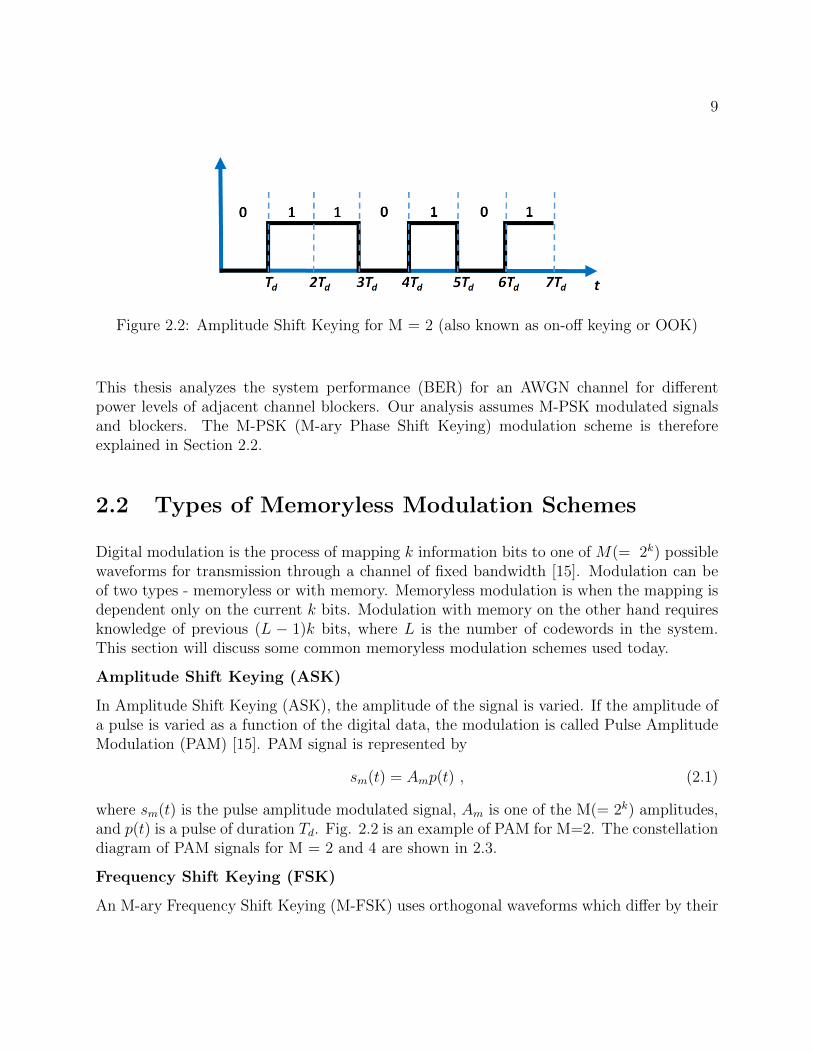
Figure 2.2: Amplitude Shift Keying for M = 2 (also known as on-off keying or OOK)
This thesis analyzes the system performance (BER) for an AWGN channel for differentpower levels of adjacent channel blockers. Our analysis assumes M-PSK modulated signalsand blockers. The M-PSK (M-ary Phase Shift Keying) modulation scheme is thereforeexplained in Section 2.2.
2.2 Types of Memoryless Modulation Schemes
Digital modulation is the process of mapping k information bits to one of M(= 2k) possiblewaveforms for transmission through a channel of fixed bandwidth [15]. Modulation can beof two types - memoryless or with memory. Memoryless modulation is when the mapping isdependent only on the current k bits. Modulation with memory on the other hand requiresknowledge of previous (L − 1)k bits, where L is the number of codewords in the system.This section will discuss some common memoryless modulation schemes used today.
Amplitude Shift Keying (ASK)
In Amplitude Shift Keying (ASK), the amplitude of the signal is varied. If the amplitude ofa pulse is varied as a function of the digital data, the modulation is called Pulse AmplitudeModulation (PAM) [15]. PAM signal is represented by
sm(t) = Amp(t) , (2.1)
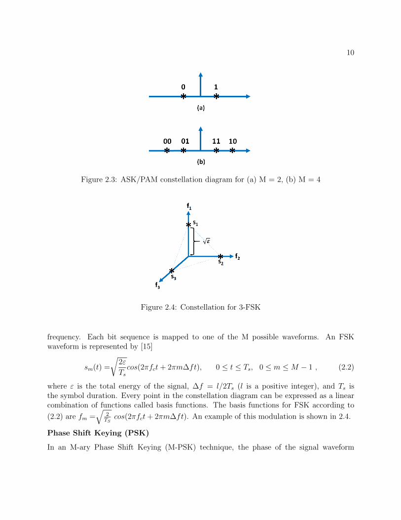
where sm(t) is the pulse amplitude modulated signal, Am is one of the M(= 2k) amplitudes,and p(t) is a pulse of duration Td. Fig. 2.2 is an example of PAM for M=2. The constellationdiagram of PAM signals for M = 2 and 4 are shown in 2.3.
Frequency Shift Keying (FSK)
An M-ary Frequency Shift Keying (M-FSK) uses orthogonal waveforms which differ by their
10
Figure 2.3: ASK/PAM constellation diagram for (a) M = 2, (b) M = 4
Figure 2.4: Constellation for 3-FSK
frequency. Each bit sequence is mapped to one of the M possible waveforms. An FSKwaveform is represented by [15]
sm(t) =
√2ε
Tscos(2πfct+ 2πm∆ft), 0 ≤ t ≤ Ts, 0 ≤ m ≤M − 1 , (2.2)
where ε is the total energy of the signal, ∆f = l/2Ts (l is a positive integer), and Ts isthe symbol duration. Every point in the constellation diagram can be expressed as a linearcombination of functions called basis functions. The basis functions for FSK according to
(2.2) are fm =√
2TS
cos(2πfct+ 2πm∆ft). An example of this modulation is shown in 2.4.
Phase Shift Keying (PSK)
In an M-ary Phase Shift Keying (M-PSK) technique, the phase of the signal waveform

11
Figure 2.5: Constellation diagram for (a) M = 4, (b) M = 8
is changed. Each signal has same symbol energy of εs. M-PSK signals are commonlyrepresented as
si(t) =√εscos
(2π
Mi
)f1︸ ︷︷ ︸
In-phase component
−√εssin
(2π
Mi
)f2︸ ︷︷ ︸
Quadrature component
, i = 0, 2...,M − 1 (2.3)
where f1 and f2 are orthonormal basis functions: f1 =√
2Tscos(2πfct) and f2 =
√2Tssin(2πfct)
for t ∈ [0, TS]. The constellation diagrams for M = 4 (QPSK), and M = 8 (8-PSK) areshown in 2.5.
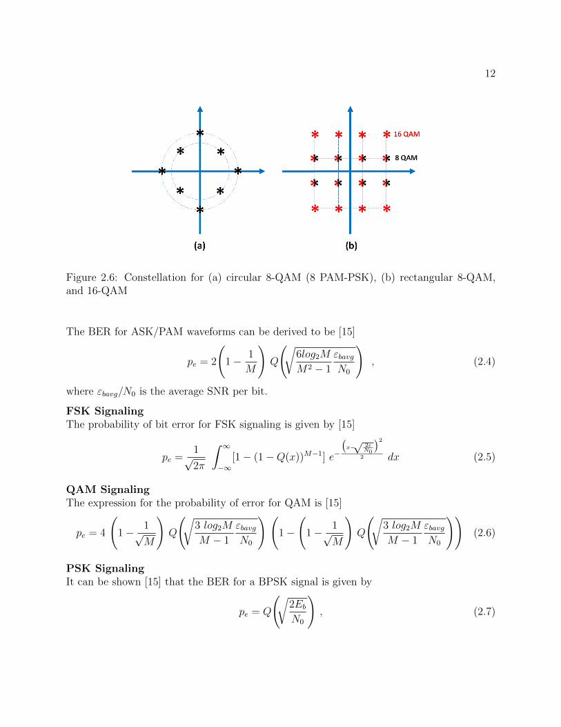
Quadrature Amplitude Modulation (QAM)
In Quadrature Amplitude Modulation, information is conveyed through its amplitude andphase. QAM can be represented in two ways - rectangular QAM or circular QAM (PAM-PSK). An example is shown in 2.6. The symbols in QAM do have the same energy.
2.3 System Performance for Memoryless Modulation
Schemes
In this section we consider the BER expressions for ASK/PAM, FSK, QAM, and M-PSK inan AWGN channel.
ASK/PAM Signaling
12
Figure 2.6: Constellation for (a) circular 8-QAM (8 PAM-PSK), (b) rectangular 8-QAM,and 16-QAM
The BER for ASK/PAM waveforms can be derived to be [15]
pe = 2
(1− 1
M
)Q
(√6log2M
M2 − 1
εbavgN0
), (2.4)
where εbavg/N0 is the average SNR per bit.
FSK SignalingThe probability of bit error for FSK signaling is given by [15]
pe =1√2π
∫ ∞−∞
[1− (1−Q(x))M−1] e−
(x−√
2εN0
)22 dx (2.5)
QAM SignalingThe expression for the probability of error for QAM is [15]
pe = 4
(1− 1√
M
)Q
(√3 log2M
M − 1
εbavgN0
) (1−
(1− 1√
M
)Q
(√3 log2M
M − 1
εbavgN0
))(2.6)
PSK SignalingIt can be shown [15] that the BER for a BPSK signal is given by
pe = Q
(√2EbN0
), (2.7)

13
where pe is the probability of error, Eb is the energy per bit, and N0 is the noise spectraldensity. Q(x) is the Q-function and is defined as Q(x) = 1√
2π
∫∞xe−(u
2/2)du. Using Greyencoding it can be seen that the probability of error for a single bit in a QPSK symbol is
the same the probability of bit error for BPSK, that is, pb = Q
(√2EbN0
). The probability
of symbol error, pS for QPSK can be derived from the Union bound or calculated exactlyas [15]:
pS = 1−
[1−Q
(2EbN0
)]2(2.8)
pS = 2Q
(√2EbN0
)[1− 1
2Q
(√2EbN0
)](2.9)
≈ 2Q
(√2EbN0
). (2.10)
For an M-PSK signal, the symbol error rate pS can be approximated using the improvedUnion bound as [ [15]
pS = 2Q
(√(2log2M)sin2
(pi
M
)EbN0
). (2.11)
Fig. 2.7 shows the SER plot for PSK signaling, for M = 2 (BPSK), 4 (QPSK), 8, and 16.For a SER of 10−6, BPSK needs 0.24 dB less energy per bit than QPSK, 3.8 dB less than8-PSK, and 8.4 dB less than 16-PSK. The advantage of using higher order modulation isthe improvement of spectral efficiency. For these modulation schemes, the BER curves canbe approximated as 1/(number of bits)*SER. This assumes Grey mapping, that is adjacentsymbols only differ by 1 bit. Hence the BER curves for Grey mapping is given in Fig. 2.8.The actual BERs for M-PSK, will be higher for M ≥ 4.

14
Figure 2.7: SER plot for BPSK, QPSK, 8-PSK, and 16-PSK signaling.
Figure 2.8: BER plot for BPSK, QPSK, 8-PSK, and 16-PSK signaling.

Chapter 3
Signal Distortion due to Receiver RFNon-Linearity
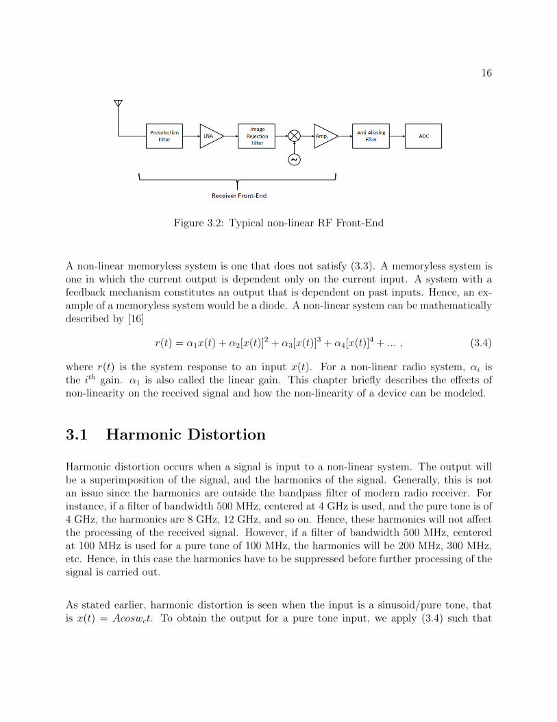
Figure 3.1 shows the part of the receiver where the non-linearity is studied, while Fig.3.2represents a typical RF non-linear front-end.
Linearity refers to homogeneity and additivity. A linear system is one in which if a given inputis altered by a scaling factor, the output of the system will also scale by an equal magnitude.The second condition for linearity is that, if an input to the system is a superimpositionof two inputs, the output will also be a superimposition of the responses corresponding tothe two inputs were, they subjected to the system individually. This is mathematicallysummarized in (3.1) - (3.3).
r1(t) = f(x1(t)) , (3.1)
r2(t) = f(x2(t)) , (3.2)
αr1(t) + βr2(t) = f [αx1(t) + βx2(t)] . (3.3)
Figure 3.1: A simplified structure of a digital communication system. The block in red isthe system under study - that is, the non-linear RF Front-End
15
16
Figure 3.2: Typical non-linear RF Front-End
A non-linear memoryless system is one that does not satisfy (3.3). A memoryless system isone in which the current output is dependent only on the current input. A system with afeedback mechanism constitutes an output that is dependent on past inputs. Hence, an ex-ample of a memoryless system would be a diode. A non-linear system can be mathematicallydescribed by [16]
r(t) = α1x(t) + α2[x(t)]2 + α3[x(t)]3 + α4[x(t)]4 + ... , (3.4)
where r(t) is the system response to an input x(t). For a non-linear radio system, αi isthe ith gain. α1 is also called the linear gain. This chapter briefly describes the effects ofnon-linearity on the received signal and how the non-linearity of a device can be modeled.
3.1 Harmonic Distortion
Harmonic distortion occurs when a signal is input to a non-linear system. The output willbe a superimposition of the signal, and the harmonics of the signal. Generally, this is notan issue since the harmonics are outside the bandpass filter of modern radio receiver. Forinstance, if a filter of bandwidth 500 MHz, centered at 4 GHz is used, and the pure tone is of4 GHz, the harmonics are 8 GHz, 12 GHz, and so on. Hence, these harmonics will not affectthe processing of the received signal. However, if a filter of bandwidth 500 MHz, centeredat 100 MHz is used for a pure tone of 100 MHz, the harmonics will be 200 MHz, 300 MHz,etc. Hence, in this case the harmonics have to be suppressed before further processing of thesignal is carried out.
As stated earlier, harmonic distortion is seen when the input is a sinusoid/pure tone, thatis x(t) = Acoswct. To obtain the output for a pure tone input, we apply (3.4) such that

17
we consider only three orders of non-linearity (that is, r(t) = α1x(t) + α2[x(t)]2 + α3[x(t)]3).Considering up until the third order term is a good approximation. Then the output is givenas [16]
r(t) =α2A
2
2+
(α1A+
3α3A3
4
)coswct+
α2A2
2cos2wct+
α3A3
4cos3wct . (3.5)
Note that due to non-linearity the gain experienced by the pure tone is not α1, rather(α1A+ 3α3A3
4
). Hence, from (3.5), we see that non-linearity of a device causes the output to
contain the input pure tone along with its harmonics. Harmonic distortion can be quantifiedas a power ratio (3.6) or by ’percentage of distortion’ (3.7) [17].
PHD = Pfundamental − Pharmonics [dBc] , (3.6)
where PHD is the harmonic distortion power ratio, Pfundamental is the power of the funda-mental tone (dB/dBm), and Pharmonics is the power contained in the harmonics (dB/dBm).If Pfundamental and Pharmonics are converted into voltage quantities, ’percentage of distortion’can be defined as in (3.7) [17].
PercentageofDistortion =VharmonicsVfundamental
× 100 % . (3.7)
3.2 Gain Compression
For pure tone inputs, we have seen that the gain of the fundamental tone after passing it to a
nonlinear device, is give by
(α1A+ 3α3A3
4
). If α1α3 > 0 (where α1 and α3 are in linear units),
the non-linear device exhibits expansive behavior where the slope (gain) of transfer functiongraph, increases as the amplitude A increases [16]. On the other hand, if α1α3 < 0, the thebehavior is compressive where the slope decreases as the amplitude A increases [16]. Mostnon-linear devices like amplifiers exhibit compressive behavior and hence attain saturationafter a given threshold of the input amplitude. For compressive behavior, we define the1-dB compression point which is associated with an input and output amplitude as shown inFig. 3.3. The 1-dB compression point is formally defined as the point at which the outputamplitude (dB) is 1-dB below the linearly amplified value for a given input amplitude (dB).For a pure tone input, the 1-dB input amplitude, Ain,1−dB is given in (3.8) [16].
Ain,1−dB =
√√√√0.145
∣∣∣∣∣α1
α3
∣∣∣∣∣ . (3.8)

18
Figure 3.3: Transfer function of a compressive amplifier on log scale
Gain compression can cause two phenomenons - loss of information in modulation schemes,and de-sensitization [16]. For modulation schemes that do not contain information in theamplitude, example - FM (Frequency Modulation), gain compression has no effect. However,for AM (Amplitude Modulation), gain compression has a significant impact since informationis contained in the amplitude.De-sensitization occurs when a large interferer is superimposed with the desired small signal.The large amplitude of the interferer reduces the gain for the small signal, causing thephenomenon of de-sensitization, which in turn reduces the signal-to-noise (SNR) ratio. Thegain experienced by the small signal in the presence of the large interferer has been derived
in [16] and is
(α1+ 3
2α3A
22
), where A2 is the amplitude of the interferer. Due to compressive
behavior (that is, α1α3 < 0, which implies that α3 is negative for a positive linear gain), asA2 increases, the gain of small signal decreases. For a sufficiently large interferer amplitude,the gain of the small signal (that is, (α1 + 3
2α3A
22)) reduces to zero, at which point the small
signal is said to be blocked [16].
19
Figure 3.4: Illustration of the transfer of modulation due to the SOI from the interferer, dueto non-linear devices
3.3 Cross Modulation
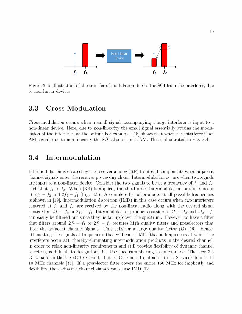
Cross modulation occurs when a small signal accompanying a large interferer is input to anon-linear device. Here, due to non-linearity the small signal essentially attains the modu-lation of the interferer, at the output.For example, [16] shows that when the interferer is anAM signal, due to non-linearity the SOI also becomes AM. This is illustrated in Fig. 3.4.
3.4 Intermodulation
Intermodulation is created by the receiver analog (RF) front end components when adjacentchannel signals enter the receiver processing chain. Intermodulation occurs when two signalsare input to a non-linear device. Consider the two signals to be at a frequency of f1 and f2,such that f1 > f2. When (3.4) is applied, the third order intermodulation products occurat 2f1 − f2 and 2f2 − f1 (Fig. 3.5). A complete list of products at all possible frequenciesis shown in [19]. Intermodulation distortion (IMD) in this case occurs when two interfererscentered at f1 and f2, are received by the non-linear radio along with the desired signalcentered at 2f1 − f2 or 2f2 − f1. Intermodulation products outside of 2f1 − f2 and 2f2 − f1can easily be filtered out since they lie far up/down the spectrum. However, to have a filterthat filters around 2f2 − f1 or 2f1 − f2 requires high quality filters and preselectors thatfilter the adjacent channel signals. This calls for a large quality factor (Q) [16]. Hence,attenuating the signals at frequencies that will cause IMD (that is frequencies at which theinterferers occur at), thereby eliminating intermodulation products in the desired channel,in order to relax non-linearity requirements and still provide flexibility of dynamic channelselection, is difficult to design for [16]. Use spectrum sharing as an example. The new 3.5GHz band in the US (CBRS band, that is, Citizen’s Broadband Radio Service) defines 1510 MHz channels [38]. If a preselector filter covers the entire 150 MHz for implicitly andflexibility, then adjacent channel signals can cause IMD [12].
20
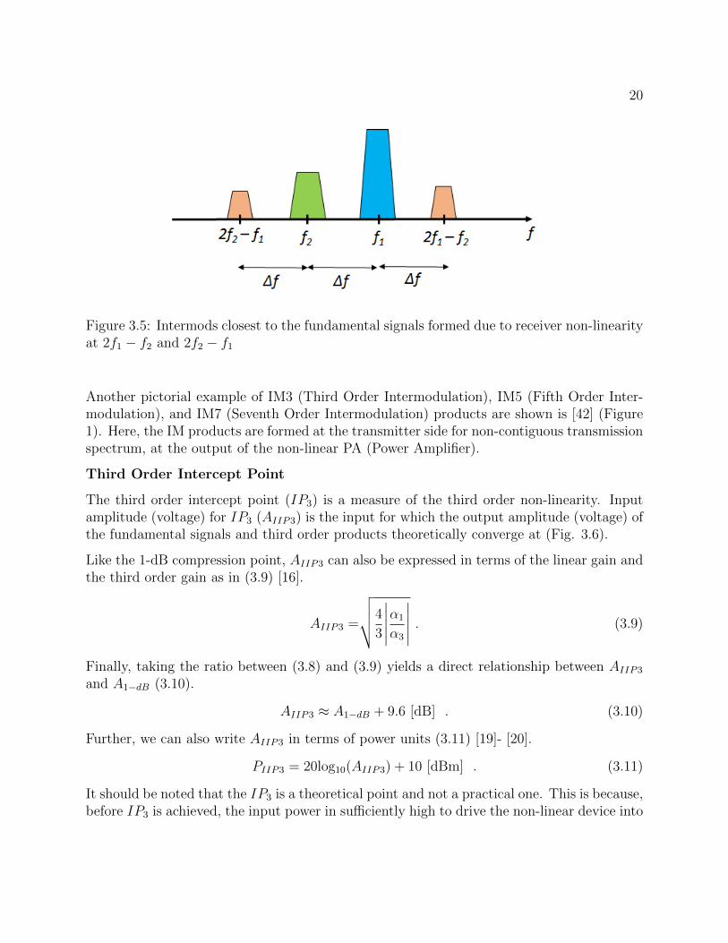
Figure 3.5: Intermods closest to the fundamental signals formed due to receiver non-linearityat 2f1 − f2 and 2f2 − f1
Another pictorial example of IM3 (Third Order Intermodulation), IM5 (Fifth Order Inter-modulation), and IM7 (Seventh Order Intermodulation) products are shown is [42] (Figure1). Here, the IM products are formed at the transmitter side for non-contiguous transmissionspectrum, at the output of the non-linear PA (Power Amplifier).
Third Order Intercept Point
The third order intercept point (IP3) is a measure of the third order non-linearity. Inputamplitude (voltage) for IP3 (AIIP3) is the input for which the output amplitude (voltage) ofthe fundamental signals and third order products theoretically converge at (Fig. 3.6).
Like the 1-dB compression point, AIIP3 can also be expressed in terms of the linear gain andthe third order gain as in (3.9) [16].
AIIP3 =
√√√√4
3
∣∣∣∣∣α1
α3
∣∣∣∣∣ . (3.9)
Finally, taking the ratio between (3.8) and (3.9) yields a direct relationship between AIIP3
and A1−dB (3.10).
AIIP3 ≈ A1−dB + 9.6 [dB] . (3.10)
Further, we can also write AIIP3 in terms of power units (3.11) [19]- [20].
PIIP3 = 20log10(AIIP3) + 10 [dBm] . (3.11)
It should be noted that the IP3 is a theoretical point and not a practical one. This is because,before IP3 is achieved, the input power in sufficiently high to drive the non-linear device into

21
Figure 3.6: Graph depicting the theoretical IP3 point. Aout, ND Ain are essentially voltagevalues.
saturation (Fig. 3.7). Hence practically, IP3 is determined through extrapolation of pointsmeasured on the linear curves (Fig. 3.7).

22
Figure 3.7: Measuring IP3 of a non-linear device through extrapolating the measured valueson the linear curves, indicated by dots. Aout, ND Ain are essentially voltage values.

Chapter 4
System Model and SER Derivations
This chapter introduces the system model. The relevant theory required has been presentedin chapters 2 and 3. Once the system model is discussed, the BER derivation for BPSK andthen higher order PSK will be presented. The derivation for BPSK is separated from thegeneral M-PSK derivation since it is possible to obtain a closed form equation for BPSK.First we assume synchronized reception of the signal of interest and blockers. However, thechapter concludes with how non-synchronous behavior is incorporated in the derivation.
4.1 System Model
Table 4.1 give a summary of the variables considered in the system model. An overview ofthe receiver system is given in Fig. 4.1. The desired signal is at frequency fc and the adjacentchannel blocking signals are at f1 and f2 such that 2f1 − f2 = fc (or 2f2 − f1 = fc) [19].The adjacent channel blockers produce intermodulation products at the desired frequency asshown in Fig. 4.3 [16], [19]. Using (3.4), the received equivalent baseband signal (complexenvelope) due to non-linearity, can then be expressed as [19]
r(t) = α1s(t) +3
2α3[b(t)]
2c(t)∗ + n(t) , (4.1)
where r(t) is the received equivalent baseband signal, s(t) is the equivalent baseband trans-mitted/desired signal, b(t) and c(t) are the equivalent baseband blocking signals, and α1 andα3 are the linear and third order gains. Using the complex envelop signal notation, (4.1) can
23

24
Table 4.1: Description of Varaibles Used in the System Model.
Variable RepresentationfC Center frequency for s(t)f1 Center frequency for blocker b(t)f2 Center frequency for blocker c(t)s(t) Modulated desired analog signal centered at fCb(t) Modulated analog interferer centered at f1c(t) Modulated analog interferer centered at f2P Transmitted power for s(t) over bandwidth WB Transmitted power for b(t) over bandwidth WC Transmitted power for c(t) over bandwidth WN Total noise power over bandwidth WM M -PSK modulation s(t)MB MB-PSK modulation b(t)MC MC-PSK modulation c(t)σn AWGN standard deviationTS Symbol period, same for all signals
b1,i ith symbol of b(t) that corresponds to the basis function f1 =√
2Tscoswct
b2,i ith symbol of b(t) that corresponds to the basis function f2 =√
2Tssinwct
c1,j jth symbol of c(t) that corresponds to the basis function f1 =√
2Tscoswct
c2,j jth symbol of c(t) that corresponds to the basis function f2 =√
2Tssinwct

25
Figure 4.1: Overview of the receiver system.
be rewritten as,
rI(t) + jrQ(t) = α1(sI(t) + jsQ(t)) (4.2)
+3
2α3[bI(t) + jbQ(t)]2(cI(t) + jcQ(t))∗ + (nI(t) + jnQ(t)),
where rI(t), sI(t), bI(t), cI(t), and nI(t) are the in-phase components and rQ(t), sQ(t), bQ(t),cQ(t), and nQ(t) the quadrature components. We further expand (4.2):
rI(t) + jrQ(t) = α1(sI(t) + jsQ(t)) +3
2α3
(((bI(t)
2 − bQ(t)2)c1 + 2bI(t)bQ(t)cQ(t)
)+
(4.3)
j
((bQ(t)2 − bI(t)2)cQ + 2bI(t)bQ(t)cI(t)
))+ (nI(t) + jnQ(t)) .
Then, the in-phase and quadrature components of the received equivalent baseband signalr(t) are given by
rI(t) = α1sI(t) +3
2α3
((bI(t)
2 − bQ(t)2)cI(t) + 2bI(t)bQ(t)cQ(t)
)+ nI(t) , (4.4)
rQ(t) = α1sQ(t) +3
2α3
((bQ(t)2 − bI(t)2)cQ(t) + 2bI(t)bQ(t)cI(t)
)+ nQ(t) .

26
Figure 4.2: Obtaining r from the received bandpass signal, rBP (t).
For PSK modulated signals, the signal state representation uses two basis functions. Properlyscaled in-phase and quadrature components can be represented in a two-dimensional vectorspace called constellation diagram. The in-phase and quadrature components are,
rI = α1sI +3
2α3
((b2I − b2Q)cI + 2bIbQcQ
)+ nI , (4.5)
rQ = α1sQ +3
2α3
((b2Q − b2I)cQ + 2bIbQcI
)+ nQ .
Note that for rI and rQ are still a function of time, but the time index has been droppedfor clarity. In the thesis, the in-phase and quadrature phase componenet are represented bysubscripts ’1’ and ’2’ respectively. Hence, (4.5) is rewritten as,
r1 = α1s1 +3
2α3
((b21 − b22)c1 + 2b1b2c2
)+ n1 , (4.6)
r2 = α1s2 +3
2α3
((b22 − b21)c2 + 2b1b2c1
)+ n2 .
Now, the practical implementation of extracting r from the bandpass signal rBP (t) is shown.r is the signal space representation of the bandpass signal rBP (t). The bandpass signalrBP (t) is demodulated using a matched filter, followed by sampling at every TS. This givesrise to discreet set of sampled values, r. This is shown in Fig. 4.1.
For the derivation, each term is represented by voltages in (4.6). The symbol rate is beingheld constant. That is, all signals - the signal of interest and the blockers, occupy the samebandwidth W, assuming the same pulse shaping filter. Also, we assume the transmitted andblocker signals to be M-PSK modulated in an AWGN channel. P is the transmit power for
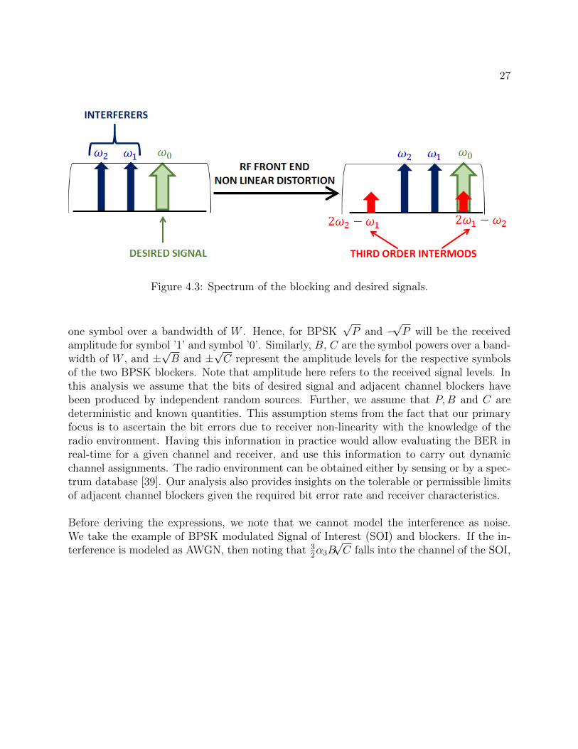
27
Figure 4.3: Spectrum of the blocking and desired signals.
one symbol over a bandwidth of W . Hence, for BPSK√P and −
√P will be the received
amplitude for symbol ’1’ and symbol ’0’. Similarly, B, C are the symbol powers over a band-width of W , and ±
√B and ±
√C represent the amplitude levels for the respective symbols
of the two BPSK blockers. Note that amplitude here refers to the received signal levels. Inthis analysis we assume that the bits of desired signal and adjacent channel blockers havebeen produced by independent random sources. Further, we assume that P,B and C aredeterministic and known quantities. This assumption stems from the fact that our primaryfocus is to ascertain the bit errors due to receiver non-linearity with the knowledge of theradio environment. Having this information in practice would allow evaluating the BER inreal-time for a given channel and receiver, and use this information to carry out dynamicchannel assignments. The radio environment can be obtained either by sensing or by a spec-trum database [39]. Our analysis also provides insights on the tolerable or permissible limitsof adjacent channel blockers given the required bit error rate and receiver characteristics.
Before deriving the expressions, we note that we cannot model the interference as noise.We take the example of BPSK modulated Signal of Interest (SOI) and blockers. If the in-terference is modeled as AWGN, then noting that 3
2α3B√C falls into the channel of the SOI,

28
Figure 4.4: BER plot for when inteference is considered as noise
we have the bit error rate as,
BER = Q
(α1
√2P√
N +
(32α3B√C
)2
)(4.7)
= Q
(α1
√2P√
N + 94(α3)2B2C
)
Then for the example of N = -114 dB, and B = C = -59 dB, and PIIP3 = -20 dBm, the BERplot is as given in Fig.4.4. Later we will show that for blockers received with random phaseoffset w.r.t. the signal of interest, the BER curves are approximately the same - irrespectiveof the modulation of the blockers. Hence, as can be seen from the figure, (4.7) is a goodapproximation for random phase blockers up until approximately 6-7 dB Eb/N0, after whichthe curves diverge. Hence a new theoretical expression is needed to accurately describe theeffect of blockers on the BER. Equation (4.7) is inaccurate if synchronized blockers, that is,blocker signals received phased synchronized with the signal of interest, are considered.
Above we have considered strong interferers/blockers in adjacent channels, which are neededto have an effect on the BER as will be shown later. Signals, blockers or other interferersfrom other cells, re-utilizing the same channel as the signals and blockers (considered above),will be much lower in power and will not affect the system performance due to intermodu-lation distortion.
29
Finally, we also see that though blockers should not be modeled as noise, we model out-of-cell signals as noise. We know that the noise is the addition of random signals - in-bandand adjacent channels. This is the measured noise floor. If the co-channel interference poweris high, we would not use those channels to begin with. However, if blockers are modulatedsignals in the adjacent channel and their signal power is strong with respect to the SOI, theycannot be modeled as noise. And this is the essence of the thesis, where high power blockersin the adjacent channels are studied and their effect on the performance of the system witha non-linear RF front-end is analyzed. Such high blocker signals can stem from TV stationsor radars, which are typical primary users in today’s shared and unlicensed bands [40].
4.2 Assumptions
The following are the assumptions made:
• An AWGN channel is considered
• All the signals are assumed to be of PSK modulation
• The signals are modulated to have the same symbol duration
• All symbols, desired and blockers, are synchronously received at the receiver of thedesired signal. This assumption is relaxed in 4.5
• We assume operation in the weak non-linear region. In particular, the ADC’s dynamicrange is not the limiting factor
4.3 BER Analysis for BPSK
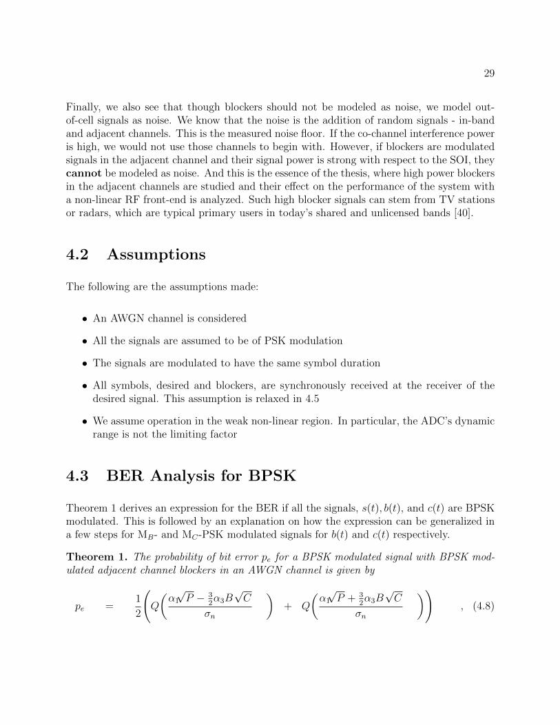
Theorem 1 derives an expression for the BER if all the signals, s(t), b(t), and c(t) are BPSKmodulated. This is followed by an explanation on how the expression can be generalized ina few steps for MB- and MC-PSK modulated signals for b(t) and c(t) respectively.
Theorem 1. The probability of bit error pe for a BPSK modulated signal with BPSK mod-ulated adjacent channel blockers in an AWGN channel is given by
pe =1
2
(Q
(α1
√P − 3
2α3B√C
σn
)+ Q
(α1
√P + 3
2α3B√C
σn
)), (4.8)
30
where Q(x) = 1√2π
∫∞x
(−u2
2
)du is the Q-function, α1 is the linear gain, α3 is the third order
gain, P,B,C are the received powers over bandwidth W of the desired signal and the twoblocking signals, and σn is the standard deviation of AWGN for the bandwidth W.
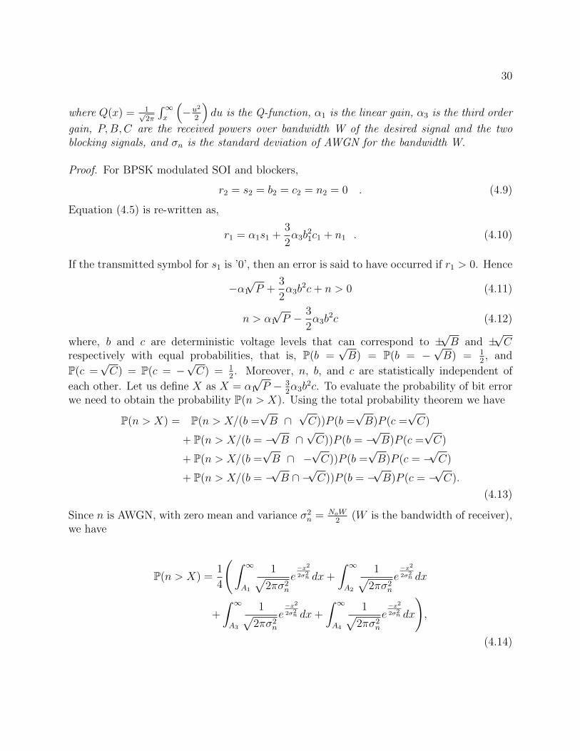
Proof. For BPSK modulated SOI and blockers,
r2 = s2 = b2 = c2 = n2 = 0 . (4.9)
Equation (4.5) is re-written as,
r1 = α1s1 +3
2α3b
21c1 + n1 . (4.10)
If the transmitted symbol for s1 is ’0’, then an error is said to have occurred if r1 > 0. Hence
−α1
√P +
3
2α3b
2c+ n > 0 (4.11)
n > α1
√P − 3
2α3b
2c (4.12)
where, b and c are deterministic voltage levels that can correspond to ±√B and ±
√C
respectively with equal probabilities, that is, P(b =√B) = P(b = −
√B) = 1
2, and
P(c =√C) = P(c = −
√C) = 1
2. Moreover, n, b, and c are statistically independent of
each other. Let us define X as X = α1
√P − 3
2α3b
2c. To evaluate the probability of bit errorwe need to obtain the probability P(n > X). Using the total probability theorem we have
P(n > X) = P(n > X/(b =√B ∩
√C))P (b =
√B)P (c =
√C)
+ P(n > X/(b = −√B ∩
√C))P (b = −
√B)P (c =
√C)
+ P(n > X/(b =√B ∩ −
√C))P (b =
√B)P (c = −
√C)
+ P(n > X/(b = −√B ∩ −
√C))P (b = −
√B)P (c = −
√C).
(4.13)
Since n is AWGN, with zero mean and variance σ2n = NoW
2(W is the bandwidth of receiver),
we have
P(n > X) =1
4
(∫ ∞A1
1√2πσ2
n
e−x2
2σ2n dx+
∫ ∞A2
1√2πσ2
n
e−x2
2σ2n dx
+
∫ ∞A3
1√2πσ2
n
e−x2
2σ2n dx+
∫ ∞A4
1√2πσ2
n
e−x2
2σ2n dx
),
(4.14)
31
where A1, A2, A3, and A4 are deterministic variables having the values
A1 = A2 = α1
√P − 3
2α3B√C , (4.15)
A3 = A4 = α1
√P +
3
2α3B√C . (4.16)
Making the substitution t = xσn
, and knowing that A1 = A2, and A3 = A4, (4.14) can becondensed to
P(n > X) =1
2
(∫ ∞A1σn
1√2πe−t22 dt+
∫ ∞A3σn
1√2πe−t22 dt
). (4.17)
Using the definition of Q-function,we obtain the probability of bit error as (4.8).
We now analyze certain specific cases of BER in relation to the blocker signal power withrespect to the power of the desired signal.
Case 1
For P << (B,C), (4.8) can be simplified to
pe =1
2
(Q
(−32α3B√C
σn
)+Q
( 32α3B√C
σn
))(4.18)
Since Q(x) = 1−Q(−x), pe = 12. Hence for very high blocker levels, reliable communication
is not possible.
Case 2
For P ≈ B ≈ C ≈ Z, we have
pe =1
2
(Q
(α1
√Z − 3
2α3Z√Z
σn
)+Q
(α1
√Z + 3
2α3Z√Z
σn
)), (4.19)
or
pe =1
2
(Q
(α1
√Z
σn
[1 +
3
2
α3
α1
Z
] )+Q
(α1
√Z
σn
[1− 3
2
α3
α1
Z
] )). (4.20)
32
Thus, receiver non-linearity plays an important role. If Z >> 1, pe = 12
(Q
(α1
√Z
σn32α3
α1Z
)+
Q
(− α1
√Z
σn32α3
α1Z
))which implies pe = 1
2.
Case 3
For P >> (B,C), pe = Q
(α1
√P
σn
)which agrees with the AWGN case without blockers when
α1 = 1.
pe = Q
(α1
√P
σn
)(4.21)
= Q
(α1
√EbW√
NoW/2
)(4.22)
= Q
(α1
√2EbNo
)(4.23)
BER Expression for an MB-PSK and MC-PSK modulation for b(t) and c(t)Equations (4.15) and (4.8), can be modified as follows
Ai,j = α1
√P − 3
2α3
((b21,i − b22,i
)c1,j + 2b1,i b2,i c2,j
), (4.24)
where bi and cj are the received voltages for basis function f1 =√
2TScoswCt. Then, for a
general MB-, MC- PSK modulation the BER is formulated as
pe =2
MBMC
MC∑j=1
MB2∑i=1
Q
(Ai,jσn
). (4.25)
4.4 SER Analysis for M-PSK
Theorem 2. The probability of symbol error pS for M-PSK modulated signal with MB-PSKand MC-PSK modulated adjacent channel blockers in an AWGN channel, where M > 2, is
33
given by
pS = 1− 1
2
(2
MBMC
)2 MC∑j=1
MB/2∑i=1
e−(m2
1,i+m22,j)
N
∫ π/M
−π/M
(1
π+
1√πN
φ eφ2
N erfc
(−φ√N
))dθ ,
(4.26)where
φ = m1,ij cosθ +m2,ij sinθ. (4.27)
M, MB, and MC represent the order of PSK modulation, where M, MB, and MC > 2. m1,ij
and m2,ij are the means and are defined as
m1,ij = α1
√P +
3
2α3
((b21,i − b22,i
)c1,j + 2b1,i b2,i c2,j
)(4.28)
m2,ij =3
2α3
((b22,i − b21,i
)c2,j + 2b1,i b2,i c1,j
)(4.29)
α1 is the linear gain, α3 is the third order gain, P,B,C are the received energy per symbol ofthe desired signal and the two blocking signals, and σn is the standard deviation of AWGN. b1,i
is the ith symbol corresponding to the basis function, f1 =√
2Tscoswct, and b2,i is the ith symbol
corresponding to the basis function, f2 =√
2Tssinwct. These are deterministic quantities since
B and C are deterministic as stated before. c1,j and c2,j follow similar interpretations.
Proof. Consider an M-PSK signal (M > 2). From (4.1), the received signal componentcorresponding to basis function f1 and f2 are:
r1 = α1s1 +3
2α3
((b21 − b22)c1 + 2b1b2c2
)+ n1 , (4.30)
r2 = α1s2 +3
2α3
((b22 − b21)c2 + 2b1b2c1
)+ n2 . (4.31)
r1 and r2 are Gaussian random variables and can be evaluated using the total probabilitytheorem as follows:
P(r1) =
MC∑j=1
MB∑i=1
P(r1/ b1,i ∩ c1,j) P(b1,i) P(c1,j) , (4.32)
=
MC∑j=1
MB∑i=1
P(r1/ b1,i ∩ c1,j)1
MB
1
MC
, (4.33)

34
where b1,i is a squared term in r1 and hence for a given c1,j, b1,i has a corresponding ± valueresulting is the same equation for r1. Hence, for a given c1,j , r1 occurs twice giving rise to
a factor of 2 and the summation for b(t) is now reduced to∑MB/2
i=1 :
P(r1) =
MC∑j=1
MB/2∑i=1
P(r1/ b1,i ∩ c1,j) 21
MBMC
. (4.34)
Since r1 is Gaussian, it has mean m1,ij which for a given transmitted symbol of s(t) (let usassume the symbol transmitted is (
√P , 0)) is defined as
m1,ij = α1
√P +
3
2α3
((b21,i − b22,i
)c1,j + 2b1,i b2,i c2,j
). (4.35)
Since every pair of (b1,i , b2,i) and (c1,j , c2,j) corresponds to one m1,ij , we can write P(r1) as
P(r1) =1√
2πσ2n
MC∑j=1
MB/2∑i=1
e−
(r1−m1,ij)2
2σ2n2
MBMC
, (4.36)
where σ2n = N
2= NoW
2, and No and W are the power spectral density and bandwidth
respectively.
Now, P(r) is given as
P(r) = P(r1, r2) = P(r1|r2)P(r2) (4.37)
=
(2
MBMC
)1
2πσn
(Mc∑j=1
Mb/2∑i=1
e−
(r1−m1,ij)2
2σ2n
)(Mc∑j=1
Mb/2∑i=1
e−
(r2−m2,ij)2
2σ2n
),
(4.38)
where m2,ij is defined as
m2,ij =3
2α3
((b22,i − b21,i
)c2,j + 2b1,i b2,i c1,j
). (4.39)
Let us evaluate P(r) for one pair of (m1,ij ,m2,ij), that is, (mX ,mY ). We then have
p′(r) =
(2
MBMC
)1
πNe−
(r1−mX )2
N e−(r2−mY )2
N . (4.40)

35
We can convert (4.40) to polar coordinates (the conversion is shown in Appendix A) toobtain
pθ,v(θ, v) =
(2
MBMC
)1
πNve−
(v−φ)2−φ2+(m2X+m2
Y )
N , (4.41)
where φ = mX cosθ +mY sinθ. Integrating v out we have
pθ(θ) =
(2
MBMC
)1
πNe−−φ2+(m2
X+m2Y )
N
∫ ∞0
ve−(v−φ)2−φ2+(m2
X+m2Y )
N , (4.42)
pθ(θ) =
(2
MBMC
)1
πNe−−φ2+(m2
X+m2Y )
N
(N
2e−
φ2
N +
√πN
2φ erfc
(− φ√
N
)), (4.43)
=1
2
(2
MBMC
)e−(m2
X+m2Y )
N
(1
π+
1√πN
φ eφ2
N erfc
(−φ√N
)), (4.44)
where erfc(x) = 2√π
∫∞xe−u22 du is called the complementary error function. A complete
evaluation of (4.43) is given in Appendix B. If p′correct represents the probability that thecorrect symbol is evaluated by the receiver, we have
p′correct =1
2
(2
MBMC
)e−(m2
X+m2Y )
N
∫ π/M
θ=−π/M
(1
π+
1√πN
φ eφ2
N erfc
(−φ√N
))dθ , (4.45)
It is to be noted that, φ = mX cosθ +mY sinθ and hence is not a constant. If the above isperformed for every pair of (m1,ij ,m2,ij), we have
pcorrect =1
2
(2
MBMC
)MC∑j=1
MB/2∑i=1
e−(m2
X+m2Y )
N
∫ π/M
θ=−π/M
(1
π+
1√πN
φ eφ2
N erfc
(−φ√N
))dθ .
(4.46)
Finally the probability of symbol error is obtained as
pS = 1− pcorrect (4.47)
= 1−
(1
MBMC
)MC∑j=1
MB/2∑i=1
e−(m2
1,ij+m22,ij)
N
∫ π/M
θ=−π/M
(1
π+
1√πN
φ eφ2
N erfc
(−φ√N
))dθ ,
(4.48)
where φ = m1,ij cosθ +m2,ij sinθ.
36
The probability of bit error for Grey Coding can be approximated as
pb =pS
log2M(4.49)
=1− pcorrectlog2M
(4.50)
=1
log2M
{1−
(1
MBMC
)× (4.51)
MC∑j=1
MB/2∑i=1
e−(m2
1,ij+m22,ij)
N
∫ π/M
θ=−π/M
(1
π+
1√πN
φ eφ2
N erfc
(−φ√N
))dθ
}. (4.52)
4.5 Non-Synchronous Reception of Blockers
We assume that the signal and blockers have the same symbol time and that there is nosignificant frequency offset of the carriers. To incorporate phases change, let us assume thatthe SOI (Signal Of Interest) does not undergo phase change w.r.t. the transmitted signal,but the blockers do. Then, before applying the power levels to the equations above, thein-phase and quadrature components should be multiplied by ejδ. That is
bi = (b1,i + jb2,i)ejδb (4.53)
cj = (c1,j + jc2,j)ejδc . (4.54)
Then the term b2i c∗j becomes,
b2i c∗j =
(kcosδ − lsinδ
)+ j
(ksinδ + lcosδ
), (4.55)
where,
δ = 2δb − δc , (4.56)
k =
(b21 − b22
)c1 + 2b1b2c2 ,
l =
(b22 − b21
)c2 + 2b1b2c1 .
Hence, we now replace k and l in (4.5) with (k cosδ−l sinδ) and (k sinδ+l cosδ) respectively.
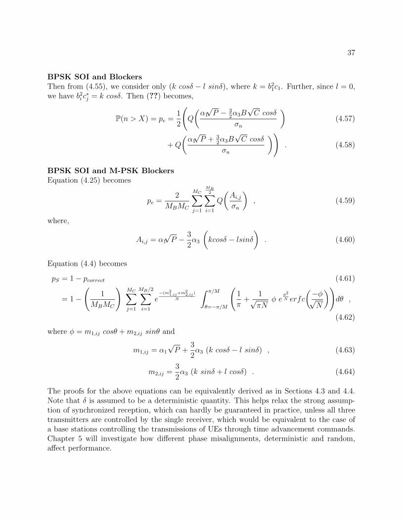
37
BPSK SOI and BlockersThen from (4.55), we consider only (k cosδ − l sinδ), where k = b21c1. Further, since l = 0,we have b2i c
∗j = k cosδ. Then (??) becomes,
P(n > X) = pe =1
2
(Q
(α1
√P − 3
2α3B√C cosδ
σn
)(4.57)
+Q
(α1
√P + 3
2α3B√C cosδ
σn
)). (4.58)
BPSK SOI and M-PSK BlockersEquation (4.25) becomes
pe =2
MBMC
MC∑j=1
MB2∑i=1
Q
(Ai,jσn
), (4.59)
where,
Ai,j = α1
√P − 3
2α3
(kcosδ − lsinδ
). (4.60)
Equation (4.4) becomes
pS = 1− pcorrect (4.61)
= 1−
(1
MBMC
)MC∑j=1
MB/2∑i=1
e−(m2
1,ij+m22,ij)
N
∫ π/M
θ=−π/M
(1
π+
1√πN
φ eφ2
N erfc
(−φ√N
))dθ ,
(4.62)
where φ = m1,ij cosθ +m2,ij sinθ and
m1,ij = α1
√P +
3
2α3 (k cosδ − l sinδ) , (4.63)
m2,ij =3
2α3 (k sinδ + l cosδ) . (4.64)
The proofs for the above equations can be equivalently derived as in Sections 4.3 and 4.4.Note that δ is assumed to be a deterministic quantity. This helps relax the strong assump-tion of synchronized reception, which can hardly be guaranteed in practice, unless all threetransmitters are controlled by the single receiver, which would be equivalent to the case ofa base stations controlling the transmissions of UEs through time advancement commands.Chapter 5 will investigate how different phase misalignments, deterministic and random,affect performance.
38
Figure 4.5: Constellation for received BPSK modulated SOI corrupted by M-PSK modulatedblockers and AWGN.
4.6 Union Bound and Improved Union Bound
The union bound and improved union bound provide practical approximations of the exactSER and BER in classic communications theory [15]. Hence, we derive the expressions forthe given case of M-PSK signals and M-PSK blockers in AWGN channels to compare themagainst the exact solutions.These upper bounds are obtained from evaluating the pairwise probabilities between onesymbol and all others (union bound) and between one symbol and the closest neighbors(improved union bound). The same approach is applied here. For a BPSK modulated SOIand M-PSK modulated blockers, assume the transmitted symbol is s1 which represents a ’0’(Fig.4.5). Then the upper bound for the probability of symbol error (or bit error since thesymbols are BPSK modulated) for linear gain of 1 (α1) is given by
pe = P(n+3
2α3 b
2i cj >
d122
) (4.65)
=2
MBMC
MC∑j=1
MB/2∑i=1
Q
( d122− 3
2α3
((b21,i − b22,i)c1,j + 2b1,ib2,ic2,j
)σn
)(4.66)
pe =2
MBMC
MC∑j=1
MB/2∑i=1
Q
(d12 − 3 α3
((b21,i − b22,i)c1,j + 2b1,ib2,ic2,j
)2σn
)(4.67)
Equation (4.67) implies that the blocker powers are in the same dimension as the signal,that is, the blockers and signal of interest use the same modulation and are received phasesynchronized. When applying this upper bound to, for example QPSK SOI, if the blockersare BPSK modulated, (4.67) is modified as
pe =2
MBMC
MC∑j=1
MB/2∑i=1
Q
(d12 − 3 α3
((b21,i − b22,i)c1,j + 2b1,ib2,ic2,j
)cosθ
2σn
), (4.68)

39
where cosθ accounts for the projection of the blocker powers in the direction of the pair ofsymbols considered.
Next, using (4.68) we derive the union and and improved union bounds for QPSK mod-ulated SOI, and (i) BPSK modulated blockers, (ii) QPSK modulated blockers.
QPSK Modulated SOI, and BPSK Modulated Blockers
The bit error rate for BPSK modulated SOI and BPSK modulated blockers is given by
pe =1
2
{Q
(√d2122N− 3
2α3 B
√2C
Ncosθ
)+Q
(√d2122N
+3
2α3 B
√2C
Ncosθ
)}. (4.69)
Then the symbol error rate for QPSK SOI (union bound) is given as
ps ≤1
2
{2
(Q
(√P
N− 3
2α3 B
√2C
N
)+Q
(√P
N+
3
2α3 B
√2C
N
))(4.70)
+Q
(√2P
N− 3
2α3 B
√2C
Ncos45o
)
+Q
(√2P
N+
3
2α3 B
√2C
Ncos45o
)}.
Further the symbol error rate for QPSK SOI (improved union bound) is given as
ps ≤1
2
{2
(Q
(√P
N− 3
2α3 B
√2C
N
)+Q
(√P
N+
3
2α3 B
√2C
N
))}. (4.71)
QPSK Modulated SOI, and QPSK Modulated Blockers
Again, we use (4.68) to derive bit error probability for BPSK modulated SOI and QPSKmodulated blockers. From here, we derive the union bound symbol error rate for QPSKmodulated SOI with QPSK modulated blockers as
ps ≤1
4
{2
(Q
(√P
N− 3
2α3 B
√2C
N
)+Q
(√P
N+
3
2α3 B
√2C
N
)(4.72)
+ 2Q
(√P
N
))+Q
(√2P
N− 3
2α3 B
√2C
N
)
+Q
(√2P
N+
3
2α3 B
√2C
N
)+ 2Q
(√2P
N
)}.

40
Figure 4.6: SER plots comparing union bound, improved union bound, and theoretical curvesfor QPSK modulated SOI and BPSK modulated blockers
The improved union bound is,
ps ≤1
4
{2
(Q
(√P
N− 3
2α3 B
√2C
N
)+Q
(√P
N+
3
2α3 B
√2C
N
)(4.73)
+ 2Q
(√P
N
))}.
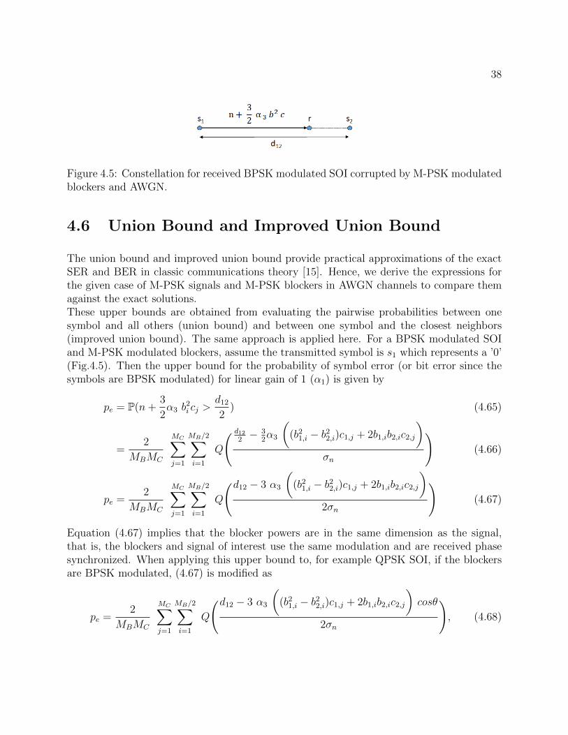
Figures 4.6 and 4.7 compare the plots for union bound and improved union bound withthe previously derived exact SER curves. In both figures we see that the improved unionbound is a good approximation until nearly 5-6 dB Eb/N0, after which the curve deviatesfrom the exact SER curve. At about SER = 10−4, both plots have a constant deviation ofapproximately 0.6 dB. In conclusion using the improved union bound, provides a reasonableapproximation within nearly 0.6 dB for both cases (Figs. 4.6 and 4.7).
4.7 Limitations of the Model and Expressions
In the above expressions, δ has been assumed to be deterministic. A more general expressionwould involve considering δ to be a random variable. Chapter 5 will show the simulated SERcurves where δ is random. Though an expression was not derived for random δ, Chapter 5talks about how this limitation in the theoretical derivation can be resolved. This section
41
Figure 4.7: SER plots comparing union bound, improved union bound, and theoretical curvesfor QPSK modulated SOI and blockers
qualitatively discusses the effects of random phase, random power, and random frequencyshifts of the blockers.
4.7.1 Random Phase SER Curves
We can get the random phase SER curve by averaging the SER curves over the differentdeterministic phase offsets. The deterministic phase offset SER curves can be obtained fromthe derived theory. Figure 4.8 shows a comparison between the simulated and theoreticalrandom phase (with respect to the SOI) curves for BPSK modulated signals. They agreewell.
4.7.2 Randomize Power of Blockers
The power of blockers could be taken as a random variable. In this case, r would no longer beof Gaussian distribution since when b(t) and c(t) are themselves Gaussian, the term b(t)2c(t)will no longer be Gaussian.Hence, in order to find the probability of error, we would first have to find the probabilitydistribution of r(t) with random powered blocker levels. Once the distribution is found, asimilar procedure described in the thesis can be applied to arrive at the error probabilities.

42
Figure 4.8: Comparison between the simulated and theoretical BER curve for BPSK mod-ulated signals, when they have a random phase with respect to the SOI
4.7.3 Randomize Frequency
Intermods are caused by the true frequencies (here, true frequencies imply received frequencyat the target receiver) of the signals. The SOI or blocker signals may experience relativefrequency shifts w.r.t. the nominal values fc, f1, and f2, as a result of local oscillator driftsor other phenomena. If the blockers are not exactly at f1, and f2, the third order intermodsformed will still fall in the band of the SOI, however, the overlap will not be complete.This means that, were the blockers exactly at f1, and f2, the performance degradation willbe the most. Figure 4.9 exemplifies this.
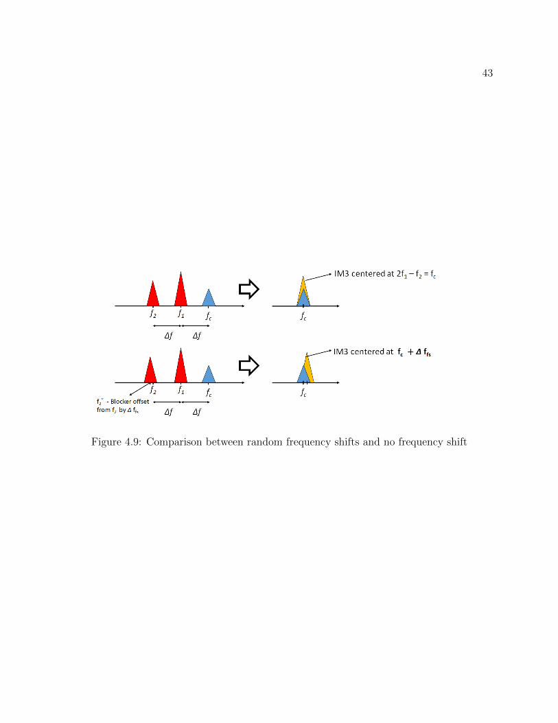
43
Figure 4.9: Comparison between random frequency shifts and no frequency shift

Chapter 5
Numerical Results and Analyses
In this chapter we present numerical results for probability of symbol error based on thederivations carried out in Chapter 4, supplemented with simulations. The objective is toevaluate and quantify the impact of receiver nonlinearity on communications system per-formance for different system parameters. We compare theoretical and simulation resultsfor various scenarios. The remainder of this chapter is divided into four sections. Section5.1 describes the power calibration. Section 5.2 outlines the simulator model that we havedeveloped. Sections 5.3 and 5.4 present the M-PSK SER results and analyses.
5.1 Power Calibration
Since we are dealing with non-linearity, we note that it is not possible to normalize the re-ceived power levels as generally done for simulations and analyses alike. More specifically, aBlocker that is 55 dB above the noise floor would have a different impact on system perfor-mance for different N0. Consequently, we cannot abstract away the radio system parameterslike operational bandwidth and noise floor. For simulation purposes, unless otherwise stated,the total noise power is set as N = −114 dBW (-84 dBm) for W = 1 MHz bandwidth ac-counting for noise floor elevation due to co-channel interference and receiver noise figure.The noise floor is high since it considers thermal noise (noise added to the received signalsby the RF receiver) and co-channel interference. The co-channel interference is consideredas the summation of a large number of random signals increasing the noise floor. And sincethe noise is a summation of a large number of random signals, the noise has a Gaussiandistribution.
44

45
The power associated with W = 1 MHz is -144 dBW (-114 dBm),
Power for 1 MHz = kTB (5.1)
= −174 dBm+ 10log10B
= −114 dBm (−144 dBW ) ,
where k is Boltzmann constant, T is the temperature (taken as 290 K), and B is the band-width.An additional 90 dB is added to account for the above mentioned elevation in noise floor.Note that in the analyses, a unit linear gain has been assumed. We consider both the desiredsignal and the adjacent channel power to be uniformly distributed across their bandwidthsof operation. Thus, for the desired signal with received power P over bandwidth W , thesignal-to-noise ratio has the same relation as the energy per symbol to noise power, that is,PN
= EsN0
. The relation between symbol energy and received signal power is given by Es = PW
,and likewise for the blockers. Table 5.1 shows the blocker power levels that are consideredin this thesis. The blocker-to-signal power ratio is obtained by subtracting the Eb/N0 fromthe blocker power relative to the noise power.
5.2 Simulator
Fig. 5.1 provides the block diagram of the simulator. Note that this does not represent theactual order of the blocks from the transmitter to the receiver. The steps involved are asfollows,
• ’X’ data points (modulation symbols) are generated for M-PSK, MB-PSK, and MC-PSK waveforms. As shown in 5.1, each data point is multiplied with its correspondingvoltage level. The voltage level accommodates for the possible phase shift the signalsexperience when transmitted through the AWGN channel.
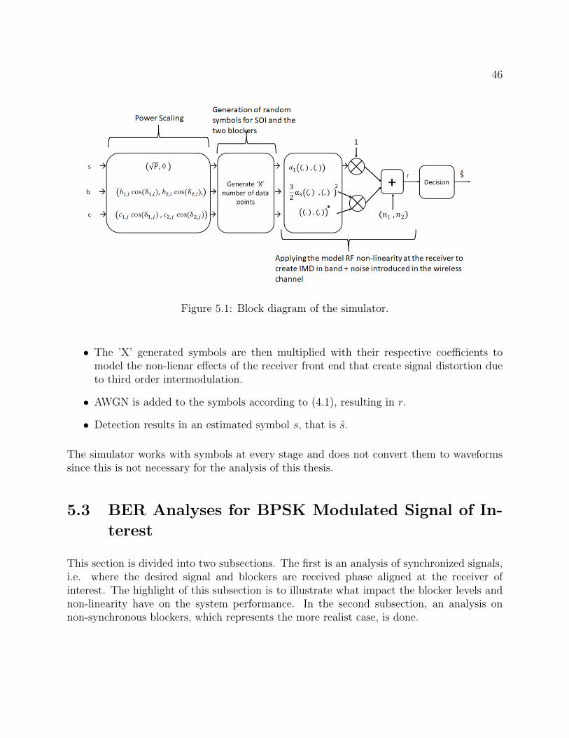
46
Figure 5.1: Block diagram of the simulator.
• The ’X’ generated symbols are then multiplied with their respective coefficients tomodel the non-lienar effects of the receiver front end that create signal distortion dueto third order intermodulation.
• AWGN is added to the symbols according to (4.1), resulting in r.
• Detection results in an estimated symbol s, that is s.
The simulator works with symbols at every stage and does not convert them to waveformssince this is not necessary for the analysis of this thesis.
5.3 BER Analyses for BPSK Modulated Signal of In-
terest
This section is divided into two subsections. The first is an analysis of synchronized signals,i.e. where the desired signal and blockers are received phase aligned at the receiver ofinterest. The highlight of this subsection is to illustrate what impact the blocker levels andnon-linearity have on the system performance. In the second subsection, an analysis onnon-synchronous blockers, which represents the more realist case, is done.

47
Figure 5.2: Theoretical BER curves for BPSK modulated signal s(t) and PIIP3 = −20 dBm,N = −114 dBW, with B = C = −59 dBW for different modulation schemes of b(t) and c(t).
5.3.1 Numerical Analyses for MB-PSK and MC-PSK ModulatedBlockers with Fixed Blocker Power Levels (Phase-SynchronousSignals)
Figure 5.2 plots theoretical, simulated and ideal (in absence of blockers) BER curves forPIIP3 = −20 dBm, and B = C = −59 dBW. The blocker power levels and the noise floor arefixed. The plot assumes BPSK modulation for s(t) and the modulation of b(t) and c(t) variesbetween BPSK, QPSK, and 8-PSK. The plots for QPSK and 8-PSK modulations for theblockers come from Theorem 1 formulated in Chapter 4. The aim of selecting the blockers tobe 55 dB above the noise floor (while Eb/N0 varies from 0 dB to 10 dB), is to consider theeffect of strong blockers that, in practice, may be because of the close vicinity of adjacentchannel transmitters and the desired receiver. Other blocker power levels are considered inthe next subsections. The following observations are made.
• The presence of blockers degrades the system performance, irrespective of the mod-ulation of the blockers. For a BER of 10−2, the worst case (when all the signals areBPSK modulated, and when b(t) is QPSK modulated, while c(t) is BPSK modulated)requires nearly 4.9 dB more energy per bit as compared to the case without blockers.

48
Even the best case (when b(t) is BPSK modulated and c(t) is 8-PSK modulated, orwhen both blockers are 8-PSK modulated), requires 3.9 dB more energy per bit whencompared to ’no blockers’ case.
• Some curves with different modulation schemes for blockers coincide. This can bejustified when observing the constellation plots. This will be further discussed in thesubsection 5.3.2.
• When the blockers are BPSK modulated, that is identical modulation with the sig-nal of interest, or when b(t) is QPSK modulated and c(t) is BPSK modulated, thesystem performance degrades the most. Other modulation schemes of blockers stillsignificantly degrades the performance.
• In general, when blockers have a modulation order greater than 2, the system perfor-mance is less affected. It can be seen from the graph that the BER is more dependenton the modulation of c(t). A higher modulation order of c(t) guarantees a lower BERcurve. This can be explained by taking a closer look at the term 3
2α3b(t)
2c(t)∗. Thepower of the term is, 9
4α23B
2C. Notice that since b(t) and c(t) will have values muchsmaller than 1 (implying B and C will also be much smaller than 1), B2 will furtherbe much smaller than C. Hence, the modualtion of c(t) plays a greater role in affect-ing the performance as compared to b(t) since its power term contributes more to thenon-linear term.
Figure 5.3 gives a comparison between the theoretical and simulated plots for a few modu-lations. It shows a good match between theory and simulations.
5.3.2 Mathematical Reasoning Behind Identical BER Performancefor Certain Modulation Orders of the Blockers
An observation made in subsection 5.3.1 was that certain combinations of blocker modulationschemes of the blockers resulted in identical BER curves. More precisely, from Fig. 5.2 themodulation orders of blockers that result in identical BER curves for a BPSK modulatedSOI are,
• BPSK modulated b(t) and BPSK modulated c(t); QPSK modulated b(t) and BPSKmodulated c(t),
• BPSK modulated b(t) and QPSK modulated c(t); QPSK modulated b(t) and QPSKmodulated c(t); 8-PSK modulated b(t) and BPSK modulated c(t),
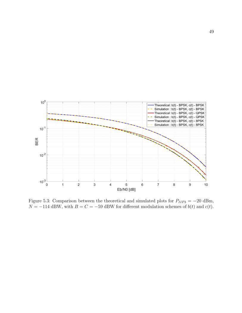
49
Figure 5.3: Comparison between the theoretical and simulated plots for PIIP3 = −20 dBm,N = −114 dBW, with B = C = −59 dBW for different modulation schemes of b(t) and c(t).

50
Figure 5.4: Constellation plot for a BPSK modulated signal, and QPSK modulated signal
• BPSK modulated b(t) and 8-PSK modulated c(t); 8-PSK modulated b(t) and 8-PSKmodulated c(t).
The identical curves can be explained by analyzing equation (4.5), and easily seen by ob-serving the effect of modulation order on the constellation diagram. Two of the above casesare explained in the remainder of the subsection.
b(t) - BPSK Modulated, c(t) - BPSK Modulated and b(t) - QPSK Modulated, c(t)- BPSK Modulated
The constellation plots for BPSK modulated and QPSK modulated signals are given in Fig.5.4. For BPSK modulated blockers and SOI, the received signal is represented as,
r1 = −α1
√P − 3
2α3b
21c1 + n1 (5.2)
The possible values that r1 can have are,
r1 = −α1
√P − 3
2α3B√C + n1 , and (5.3)
= −α1
√P +
3
2α3B√C + n1
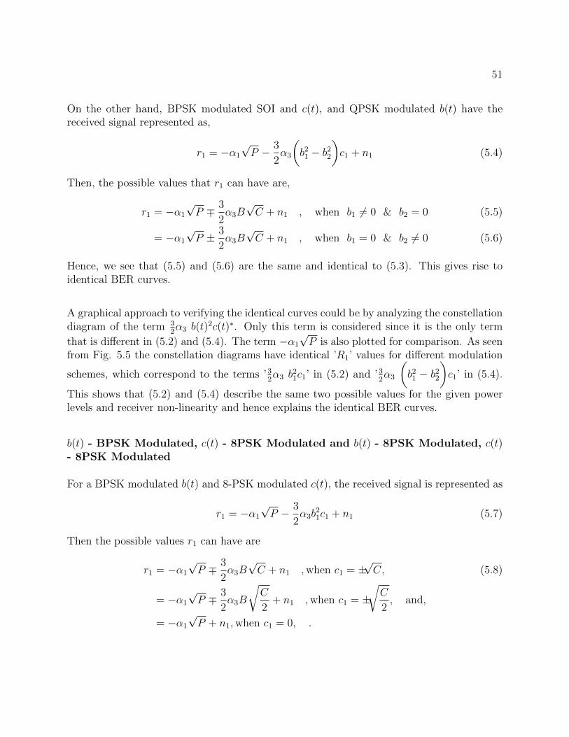
51
On the other hand, BPSK modulated SOI and c(t), and QPSK modulated b(t) have thereceived signal represented as,
r1 = −α1
√P − 3
2α3
(b21 − b22
)c1 + n1 (5.4)
Then, the possible values that r1 can have are,
r1 = −α1
√P ∓ 3
2α3B√C + n1 , when b1 6= 0 & b2 = 0 (5.5)
= −α1
√P ± 3
2α3B√C + n1 , when b1 = 0 & b2 6= 0 (5.6)
Hence, we see that (5.5) and (5.6) are the same and identical to (5.3). This gives rise toidentical BER curves.
A graphical approach to verifying the identical curves could be by analyzing the constellationdiagram of the term 3
2α3 b(t)
2c(t)∗. Only this term is considered since it is the only term
that is different in (5.2) and (5.4). The term −α1
√P is also plotted for comparison. As seen
from Fig. 5.5 the constellation diagrams have identical ’R1’ values for different modulation
schemes, which correspond to the terms ’32α3 b
21c1’ in (5.2) and ’3
2α3
(b21 − b22
)c1’ in (5.4).
This shows that (5.2) and (5.4) describe the same two possible values for the given powerlevels and receiver non-linearity and hence explains the identical BER curves.
b(t) - BPSK Modulated, c(t) - 8PSK Modulated and b(t) - 8PSK Modulated, c(t)- 8PSK Modulated
For a BPSK modulated b(t) and 8-PSK modulated c(t), the received signal is represented as
r1 = −α1
√P − 3
2α3b
21c1 + n1 (5.7)
Then the possible values r1 can have are
r1 = −α1
√P ∓ 3
2α3B√C + n1 ,when c1 = ±
√C, (5.8)
= −α1
√P ∓ 3
2α3B
√C
2+ n1 ,when c1 = ±
√C
2, and,
= −α1
√P + n1,when c1 = 0, .
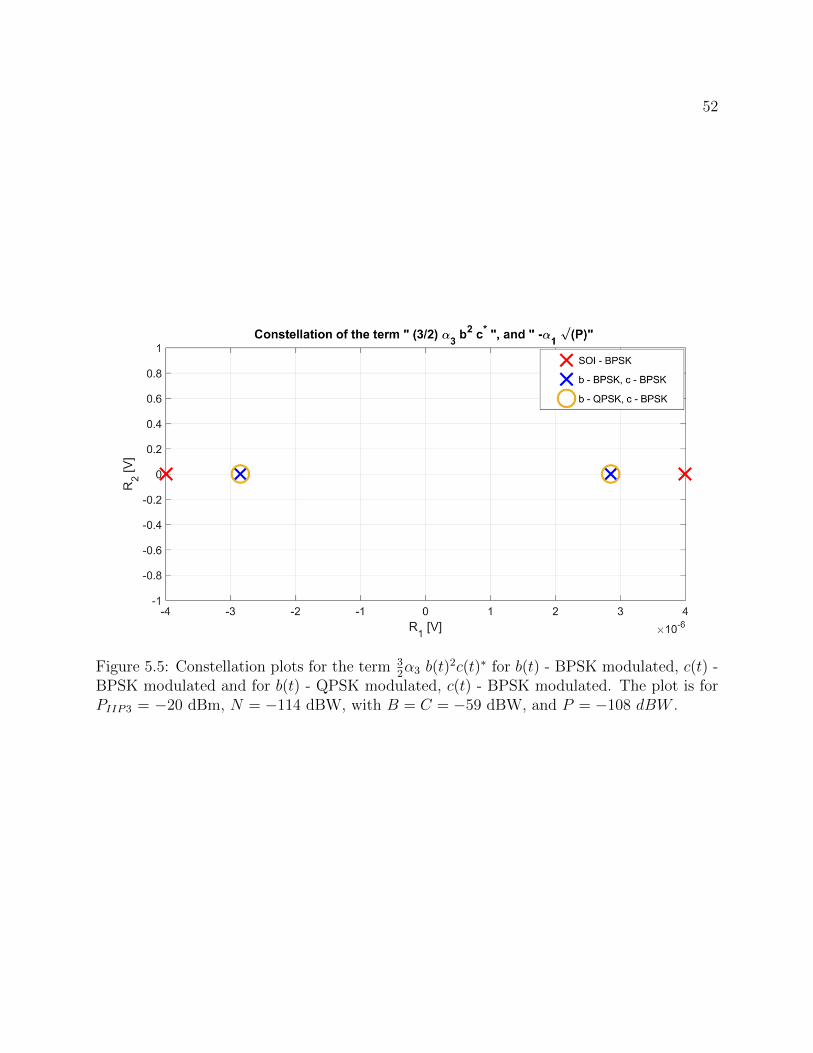
52
Figure 5.5: Constellation plots for the term 32α3 b(t)
2c(t)∗ for b(t) - BPSK modulated, c(t) -BPSK modulated and for b(t) - QPSK modulated, c(t) - BPSK modulated. The plot is forPIIP3 = −20 dBm, N = −114 dBW, with B = C = −59 dBW, and P = −108 dBW .
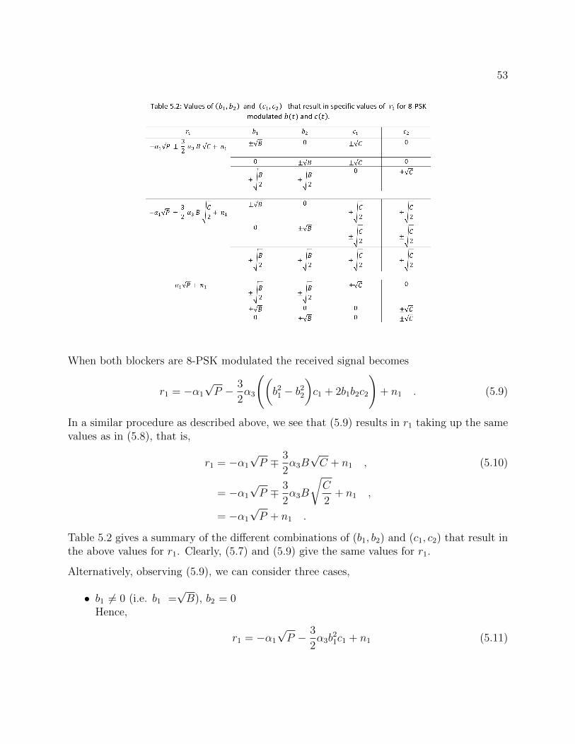
53
When both blockers are 8-PSK modulated the received signal becomes
r1 = −α1
√P − 3
2α3
((b21 − b22
)c1 + 2b1b2c2
)+ n1 . (5.9)
In a similar procedure as described above, we see that (5.9) results in r1 taking up the samevalues as in (5.8), that is,
r1 = −α1
√P ∓ 3
2α3B√C + n1 , (5.10)
= −α1
√P ∓ 3
2α3B
√C
2+ n1 ,
= −α1
√P + n1 .
Table 5.2 gives a summary of the different combinations of (b1, b2) and (c1, c2) that result inthe above values for r1. Clearly, (5.7) and (5.9) give the same values for r1.
Alternatively, observing (5.9), we can consider three cases,
• b1 6= 0 (i.e. b1 =√B), b2 = 0
Hence,
r1 = −α1
√P − 3
2α3b
21c1 + n1 (5.11)
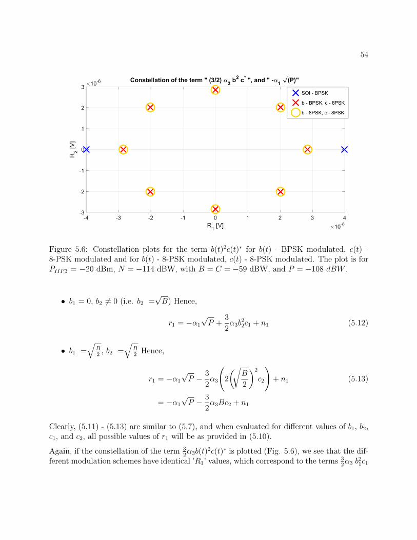
54
Figure 5.6: Constellation plots for the term b(t)2c(t)∗ for b(t) - BPSK modulated, c(t) -8-PSK modulated and for b(t) - 8-PSK modulated, c(t) - 8-PSK modulated. The plot is forPIIP3 = −20 dBm, N = −114 dBW, with B = C = −59 dBW, and P = −108 dBW .
• b1 = 0, b2 6= 0 (i.e. b2 =√B) Hence,
r1 = −α1
√P +
3
2α3b
22c1 + n1 (5.12)
• b1 =√
B2
, b2 =√
B2
Hence,
r1 = −α1
√P − 3
2α3
(2
(√B
2
)2
c2
)+ n1 (5.13)
= −α1
√P − 3
2α3Bc2 + n1
Clearly, (5.11) - (5.13) are similar to (5.7), and when evaluated for different values of b1, b2,c1, and c2, all possible values of r1 will be as provided in (5.10).
Again, if the constellation of the term 32α3b(t)
2c(t)∗ is plotted (Fig. 5.6), we see that the dif-ferent modulation schemes have identical ’R1’ values, which correspond to the terms 3
2α3 b
21c1
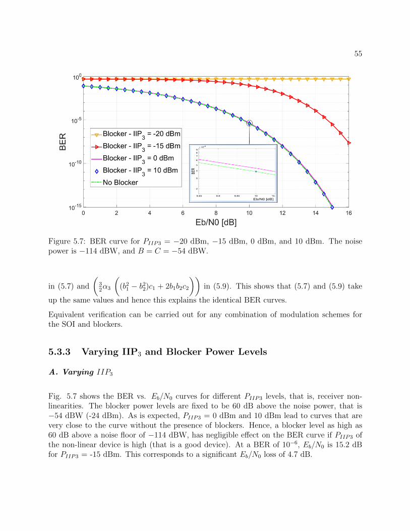
55
Figure 5.7: BER curve for PIIP3 = −20 dBm, −15 dBm, 0 dBm, and 10 dBm. The noisepower is −114 dBW, and B = C = −54 dBW.
in (5.7) and
(32α3
((b21 − b22)c1 + 2b1b2c2
))in (5.9). This shows that (5.7) and (5.9) take
up the same values and hence this explains the identical BER curves.
Equivalent verification can be carried out for any combination of modulation schemes forthe SOI and blockers.
5.3.3 Varying IIP3 and Blocker Power Levels
A. Varying IIP3
Fig. 5.7 shows the BER vs. Eb/N0 curves for different PIIP3 levels, that is, receiver non-linearities. The blocker power levels are fixed to be 60 dB above the noise power, that is−54 dBW (-24 dBm). As is expected, PIIP3 = 0 dBm and 10 dBm lead to curves that arevery close to the curve without the presence of blockers. Hence, a blocker level as high as60 dB above a noise floor of −114 dBW, has negligible effect on the BER curve if PIIP3 ofthe non-linear device is high (that is a good device). At a BER of 10−6, Eb/N0 is 15.2 dBfor PIIP3 = -15 dBm. This corresponds to a significant Eb/N0 loss of 4.7 dB.
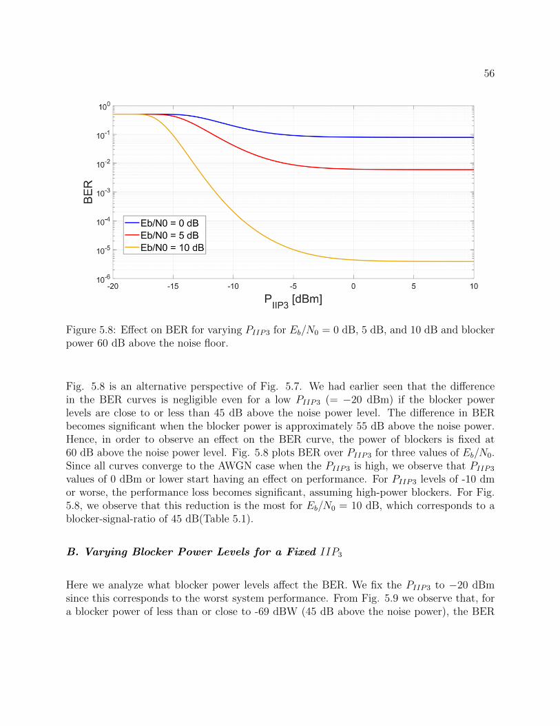
56
Figure 5.8: Effect on BER for varying PIIP3 for Eb/N0 = 0 dB, 5 dB, and 10 dB and blockerpower 60 dB above the noise floor.
Fig. 5.8 is an alternative perspective of Fig. 5.7. We had earlier seen that the differencein the BER curves is negligible even for a low PIIP3 (= −20 dBm) if the blocker powerlevels are close to or less than 45 dB above the noise power level. The difference in BERbecomes significant when the blocker power is approximately 55 dB above the noise power.Hence, in order to observe an effect on the BER curve, the power of blockers is fixed at60 dB above the noise power level. Fig. 5.8 plots BER over PIIP3 for three values of Eb/N0.Since all curves converge to the AWGN case when the PIIP3 is high, we observe that PIIP3
values of 0 dBm or lower start having an effect on performance. For PIIP3 levels of -10 dmor worse, the performance loss becomes significant, assuming high-power blockers. For Fig.5.8, we observe that this reduction is the most for Eb/N0 = 10 dB, which corresponds to ablocker-signal-ratio of 45 dB(Table 5.1).
B. Varying Blocker Power Levels for a Fixed IIP3
Here we analyze what blocker power levels affect the BER. We fix the PIIP3 to −20 dBmsince this corresponds to the worst system performance. From Fig. 5.9 we observe that, fora blocker power of less than or close to -69 dBW (45 dB above the noise power), the BER
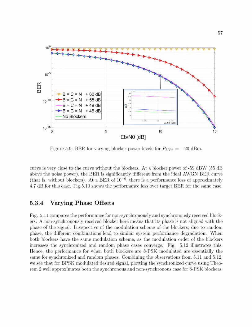
57
Figure 5.9: BER for varying blocker power levels for PIIP3 = −20 dBm.
curve is very close to the curve without the blockers. At a blocker power of -59 dBW (55 dBabove the noise power), the BER is significantly different from the ideal AWGN BER curve(that is, without blockers). At a BER of 10−6, there is a performance loss of approximately4.7 dB for this case. Fig.5.10 shows the performance loss over target BER for the same case.
5.3.4 Varying Phase Offsets
Fig. 5.11 compares the performance for non-synchronously and synchronously received block-ers. A non-synchronously received blocker here means that its phase is not aligned with thephase of the signal. Irrespective of the modulation scheme of the blockers, due to randomphase, the different combinations lead to similar system performance degradation. Whenboth blockers have the same modulation scheme, as the modulation order of the blockersincreases the synchronized and random phase cases converge. Fig. 5.12 illustrates this.Hence, the performance for when both blockers are 8-PSK modulated are essentially thesame for synchronized and random phases. Combining the observations from 5.11 and 5.12,we see that for BPSK modulated desired signal, plotting the synchronized curve using Theo-rem 2 well approximates both the synchronous and non-synchronous case for 8-PSK blockers.

58
Figure 5.10: Performance loss for B = C = −59 dBW (55 dB above the noise power). Here,the performance loss is calculated using the ’no blockers’ curve and ’B=C=N + 55 dB’ curvein Fig. 5.9
Figure 5.11: BER plots for random phase of MB-PSK and MC-PSK modulated blockers forBPSK modulated desired signal. B = C = −59 dBW (55 dB above the noise power), N =-114 dBW, and PIIP3 = -20 dBm.

59
Figure 5.12: Random and synchronized phase for BPSK modulated signal when blockers areboth QPSK, and 8-PSK modulated. B = C = −59 dBW (55 dB above the noise power), N= -114 dBW, and PIIP3 = -20 dBm.
Introducing Specific Phase Shift to BlockersConsider the blockers to be both BPSK modulated and synchronized in phase with the
desired signal. In this section we will analyze the performance of the system for when eitherb(t) or c(t) undergoes a phase shift. This is followed by analyzing what combination of phaseshifts for the blockers results in minimum performance degradation.
Figure 5.13 gives us an insight into how phase shift to c(t) affects the system performance.Note that here, it is assumed that every data point of the blocker signal goes through thesame phase shift. The system performance is the worst when c(t) are synchronized or are 180o
phase misaligned with the desired signal. On the other hand, the performance is unaffectedif the phase shift is 90o. This is easily explained if the constellation of the desired signal isconsidered. Since s(t) is a BPSK modulated signal, and the receiver is only concerned withthe power received in the dimension of its single basis function. When blockers are in-syncor 180o out if sync, all of the blocker power lies in the dimension of the desired signal. Onthe other hand, when c(t) experiences a shift of 90o, the blocker power falls perpendicular tothe dimension of the desired signal. This represents a case equivalent to the no blockers case,hence the system performance coincides with the pure AWGN case (that is, ideal theoreticalcurve with no blockers). Hence, if a system is designed where we have a 90o phase shift forBPSK modulated blockers, the presence of blockers would not cause system degradation dueto intermodulation distortion.

60
Figure 5.13: BER curves for different phase shifts in blocker c(t), assuming b(t) is synchro-nized to s(t) when all the signals are BPSK modulated. B = C = −59 dBW (55 dB abovethe noise power), N = -114 dBW, and PIIP3 = -20 dBm.
Figure 5.14 introduces specific phase shifts to b(t), while c(t) is kept synchronized with theSOI. We see here, as opposed to when c(t) was experiencing phase shifts, that the minimumdegradation corresponds to an angle of 45o. This is so because, the blocker b(t) experiencesa squaring effect due to non-linearity, as seen in (4.5). Hence, 45o phase shift on squaringgives a total phase shift of 90o for b(t)2.
Finally, Fig. 5.15 shows that if b(t) and c(t) both experience a phase shift of 90o, it leads toa performance that is equivalent to as if there were no blockers. This is so because the netphase shift experienced by b(t)2c(t)∗ is 2δb− δc (as seen from (4.56)). Figure 5.15 also showsthat a random phase of blockers is closer to the worst case of phase-synchronized blockerthan the ideal AWGN curve.

61
Figure 5.14: BER curves for different phase shifts in blocker b(t), assuming c(t) is synchro-nized to s(t) when all the signals are BPSK modulated. B = C = −59 dBW (55 dB abovethe noise power), N = -114 dBW, and PIIP3 = -20 dBm.
Figure 5.15: BER curves for 90o phase shift in blockers b(t) and c(t), when all the signalsare BPSK modulated. B = C = −59 dBW (55 dB above the noise power), N = -114 dBW,and PIIP3 = -20 dBm.
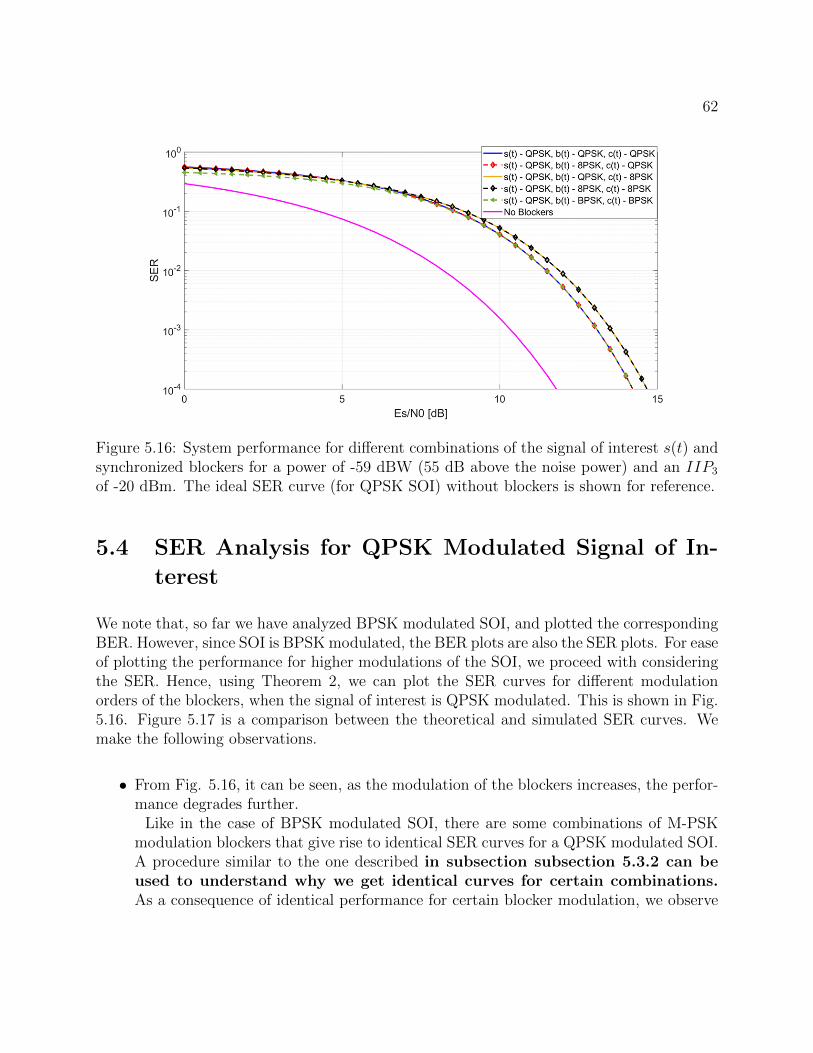
62
Figure 5.16: System performance for different combinations of the signal of interest s(t) andsynchronized blockers for a power of -59 dBW (55 dB above the noise power) and an IIP3
of -20 dBm. The ideal SER curve (for QPSK SOI) without blockers is shown for reference.
5.4 SER Analysis for QPSK Modulated Signal of In-
terest
We note that, so far we have analyzed BPSK modulated SOI, and plotted the correspondingBER. However, since SOI is BPSK modulated, the BER plots are also the SER plots. For easeof plotting the performance for higher modulations of the SOI, we proceed with consideringthe SER. Hence, using Theorem 2, we can plot the SER curves for different modulationorders of the blockers, when the signal of interest is QPSK modulated. This is shown in Fig.5.16. Figure 5.17 is a comparison between the theoretical and simulated SER curves. Wemake the following observations.
• From Fig. 5.16, it can be seen, as the modulation of the blockers increases, the perfor-mance degrades further.
Like in the case of BPSK modulated SOI, there are some combinations of M-PSKmodulation blockers that give rise to identical SER curves for a QPSK modulated SOI.A procedure similar to the one described in subsection subsection 5.3.2 can beused to understand why we get identical curves for certain combinations.As a consequence of identical performance for certain blocker modulation, we observe

63
Figure 5.17: Comparison between the theoretical and simulated SER curves for QPSK mod-ulated SOI with M-PSK synchronized modulated blockers. The blockers are plotted for apower of -59 dBW (55 dB above the noise power) and an IIP3 of -20 dBm.
Table 5.1: Es/N0 and Es/N0 losses for the corresponding SERSER Es/N0 [dB] Es/N0 loss [dB]10−1 8.6 4.410−2 11.5 3.310−4 14.2 2.4

64
the following.If the blockers have a modulation order less than or equal to that of the SOI, theSER curves are identical. Hence, the SER curves for BPSK modulated, and QPSKmodulated blockers for a QPSK modulated SOI are the same. As another example,we can also observe this in Fig. 5.20 for an 8-PSK modulated SOI with (i) QPSK, and(ii) 8-PSK modulated blockers.
• A QPSK modulated signal with synchronous QPSK blockers is worse than the idealAWGN case. We expected significant performance loss due to high power blockers,and this is what we have observed. The Es/N0 loss is 4.4 dB for an SER of 10−1 (atEs/N0 = 8.6 dB). Table 5.1 gives a summary of the losses for different SER values. Asseen from the table, the loss decreases with increasing Es/N0. This is intuitive, sincefor a fixed noise power, the power of the SOI increases with increase in SNR.
• In general, as the modulation order of the blockers increases, the SER curve becomesworse. This is a trend that is opposite to when the SOI is BPSK modulated. A qual-itative explanation is that for a BPSK modulated SOI, as the modulation order ofthe blockers increases, the energy per bit decreases for the blockers, since a constantenergy per symbol is assumed (that is, Eb = Es
M, hence when M increases, Eb decreases
since Es is constant). Hence, the interference energy per bit along a single dimensionfor the BPSK SOI decreases, giving rise to lower BER curves.
On the other hand, the increase in performance degradation for QPSK SOI, can beunderstood by comparing the two cases - QPSK modulated b(t), 8-PSK modulatedc(t) and 8-PSK modulated blockers (b(t) and c(t)). Their respective constellations forthe term 3
2α3b(t)
2c(t)∗ are shown in Figs. 5.5 and 5.6. For QPSK modulated b(t) and8-PSK modulated c(t), we see that the blocker symbols only affect the in-phase com-ponent of quadrature component of SOI (Fig. 5.5). For 8-PSK blockers on the otherhand, there is a possibility of affecting both bits of a QPSK SOI, at the same time(Fig. 5.6). This causes an 8-PSK modulated synchronized blocker to result in higherprobability of error.
• Further, Fig. 5.20 gives the SER curves for SOI with M = 2, 4, and 8. The mod-ulation order of the blockers is kept to be identical to that of the SOI. Clearly, theSER curve degrades with the presence of blockers, when the curves are compared to

65
Figure 5.18: Constellation plot for QPSK modulated signals.
Figure 5.19: Constellation plot for QPSK modulated SOI and 8-PSK modulated blocker.

66
Figure 5.20: SER curves for SOI and synchronized blockers for M = 2, 4, and 8. The AWGNcurves are shown for comparison. The blockers are plotted for a power of -59 dBW (55 dBabove the noise power) and an IIP3 of -20 dBm.
the corresponding AWGN case. More importantly, we see that the like AWGN cases,we should expect that the SER curves degrades as the modulation order of the SOIincreases, irrespective of the modulation order of the blockers. Hence, an 8-PSK mod-ulated SOI will have worse SER than a BPSK or QPSK modulated SOI, irrespectiveof the modulation order of the blockers.
• When comparing the curves to their respective AWGN curves, at SER = 10−2, theEs/N0 loss for BPSK SOI and blockers is 4.9 dB. While for QPSK modulated SOIand blockers, the loss is 3.3 dB, and for 8-PSK modulated SOI and blockers, the lossis 3.7 dB. This is so because BPSK blockers affect the BPSK modulated signal mostsince focusing the energy. However, not that orthogonal blockers can be easily createdfor this case.
Figure 5.21 plots the SER curves for phase misaligned blocker c(t). The performance de-grades, but not by much, when the signals are not phase aligned. The phase misalignmenthas little effect here, as opposed to case of BPSK signal of interest, where orthogonal blockerscan null the effect of intermodulation distortion on BER.
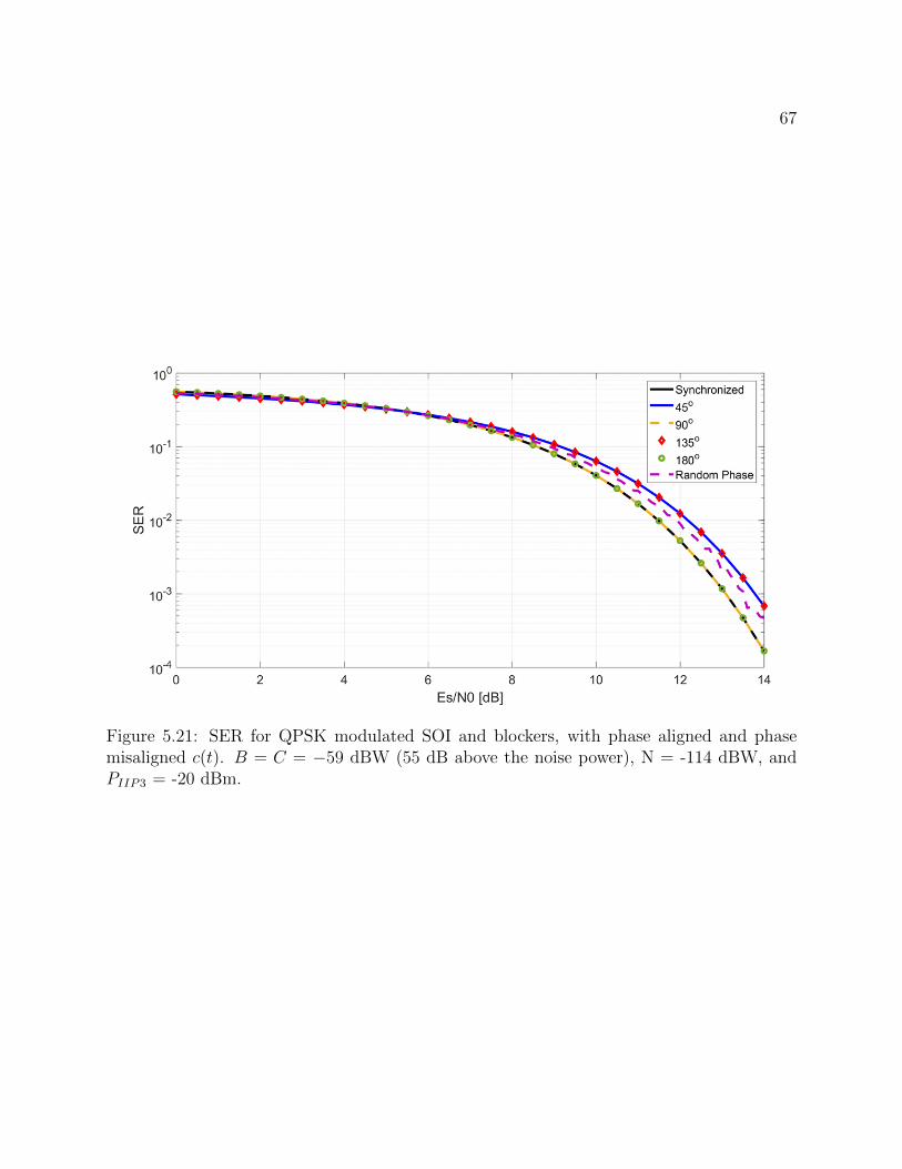
67
Figure 5.21: SER for QPSK modulated SOI and blockers, with phase aligned and phasemisaligned c(t). B = C = −59 dBW (55 dB above the noise power), N = -114 dBW, andPIIP3 = -20 dBm.
Chapter 6
Conclusions and Future Work
This thesis has shown that the presence of blockers can significantly degrade the systemperformance if the receiver is highly non-linear and the blocker signals are strong w.r.t. thedesired signal. If a BPSK message signal is considered with random phase M-PSK modulatedblockers, there can be an Eb/N0 loss of nearly 3.4 dB at a BER of 10−3 for strong blockingsignals.
We also observed the following:
• There is negligible difference between the BER performance curves for different ran-dom phase PSK modulated blockers (that is, BPSK, QPSK, 8-PSK etc.), for a BPSKmodulated s(t). Hence, knowing the performance curve of one case of PSK modulatedblockers is sufficient to analyze the performance for all PSK modulated blockers for agiven BPSK modulated s(t) (Fig. 5.11).
• The phase-synchronized and phase-unsynchronized blocker curves converge for higherorder modulation (M>4) (Fig. 5.12). In other words, the performance curve for phase-synchronized 8-PSK blockers approximates the performance for random phase MB- ,MC- PSK modulated blockers.
The above points can be generalized to M-PSK modulated SOI.
In general, the performance loss is significant for the unrealistic case of synchronously re-ceived signal and blockers. For a BPSK modulated SOI, the performance loss is lower, butnoticeable for the case where blockers are phase misaligned with a BPSK modulated SOI.However, if the system can be designed such that the blockers are orthogonal to the de-sired signal at the non-linear receiver, it is possible to completely eliminate the performancedegradation due to intermodulation distortion.
68
69
For an SOI modulation order greater than two, the performance loss further degrades forphase misaligned blockers, when compared to synchronous blockers. Hence, to have minimumperformance degradation, the blockers should either be completely in-phase, out-of-phase.
Our numerical analysis provides insights on the interplay between the adjacent channelblocker signal power, desired signal power and the receiver non-linearity. Receiver non-linearity can cause a 3 dB to 5 dB loss in Eb/N0 depending on the spectrum environmentand blocker power. Under severe scenarios (very high non-linearity and blocker power),while still operating in the weak nonlinear region, the communication link is significantlyimpaired. With increasing linearity of receivers, the BER degradation reduces considerablyeven for high blocker signal powers. This is primarily so because the multiplicative effect ofnon-linearity grows much faster than the additive/subtractive effect of blocker signal levelson distortion power. Likewise, with low-power blockers the BER degradation due to inter-modulation distortion diminishes even for highly non-linear receivers. Thus, we observedthat receiver non-linearity and signal characteristics play an important role for adjacentchannel co-existence in congested spectrum environments. Our BER expressions provide thetools to evaluate the impact of RF receiver nonlinearity on communications performance incongested and dense radio environments. Knowing the receiver characteristics, the sharedchannels can be allocated so that poor receivers experience low-power or orthogonal blockersin adjacent bands. The envisaged scenario is that of a spectrum access system (SAS) thatcentrally manages access to shared spectrum while taking into account the receiver charac-teristics. The analysis of this thesis gives insights into how to perform channel assignmentand network optimization.
The conclusions of our analysis can be summarized as follows:
1. Adjacent channel interference (blockers) can significantly impact performance of modu-lated signals when the receiver nonlinearity is poor and the received blocker power levelsare high.
2. Blockers are most effective for degrading the system performance when phase-synchronizedwith BPSK modulated signal of interest and least effective when phase-synchronized withQPSK or higher order PSK SOI.
3. Smart spectrum management (i.e. power control and spectrum allocation as a functionof the receiver characteristics) can minimize or avoid performance degradation caused byintermodulation distortion.
Our analysis can be extended and generalized to include other modulation schemes andsystem parameters. The analysis presented here is theoretical and simulations were carried

70
out using MATLAB. Hence, as a part of future work, software-defined radios (SDRs) will beused to build a testbed, create signals and blockers as assumed in this thesis and measurethe system performance for different system parameters. The system performance will becompared with the numerical results presented here.
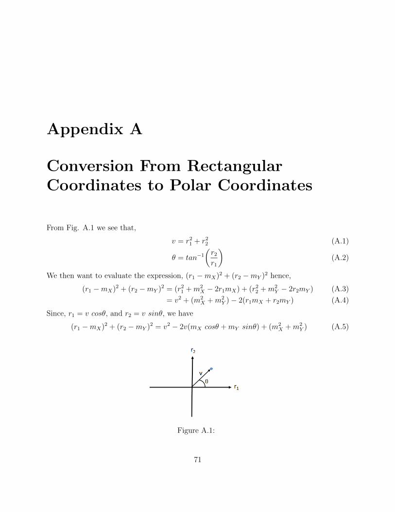
Appendix A
Conversion From RectangularCoordinates to Polar Coordinates
From Fig. A.1 we see that,
v = r21 + r22 (A.1)
θ = tan−1(r2r1
)(A.2)
We then want to evaluate the expression, (r1 −mX)2 + (r2 −mY )2 hence,
(r1 −mX)2 + (r2 −mY )2 = (r21 +m2X − 2r1mX) + (r22 +m2
Y − 2r2mY ) (A.3)
= v2 + (m2X +m2
Y )− 2(r1mX + r2mY ) (A.4)
Since, r1 = v cosθ, and r2 = v sinθ, we have
(r1 −mX)2 + (r2 −mY )2 = v2 − 2v(mX cosθ +mY sinθ) + (m2X +m2
Y ) (A.5)
Figure A.1:
71

72
Let φ = mX cosθ +mY sinθ. Completing the square we get
(r1 −mX)2 + (r2 −mY )2 = (v − φ)2 − φ2 + (m2X +m2
Y ) (A.6)

Appendix B
Integral Evaluation
We evaluate the following integral, ∫ ∞v=0
v e−(v−φ)2N dv (B.1)
Making a variable substitution, let v−φ√N
= u,∫ ∞v=0
v e−(v−φ)2N dv =
√N
∫ ∞u=−φ√
N
(√N u+ φ) e−u
2
du (B.2)
The above is evaluated using Wolfram Alpha,∫ ∞v=0
v e−(v−φ)2N dv =
N
2e−
φ2
N +√πN
φ
2
(erfc
(− φ√
N
))(B.3)
73

Bibliography
[1] Cisco Visual Networking Index: Global Mobile Data Traffic Forecast Update, 20162021,White Paper. Available: http://www.cisco.com/c/en/us/solutions/collateral/service-provider/visual-networking-index-vni/mobile-white-paper-c11-520862.pdf
[2] President’s Council of Advisors on Science and Technology (PCAST) report, Realiz-ing the Full Potential of Government-Held Spectrum to Spur Economic Growth, July2012. Available: http://www.whitehouse.gov/sites/default/files/microsites/
ostp/pcast_spectrum_report_final_july_20_2012.pdf
[3] S. M. Dudley, et. al., “Practical Issues for Spectrum Management With Cognitive Ra-dios,” Proceedings of the IEEE, vol. 102, no. 3, pp. 242-264, 2014.
[4] T. M. Taher, R. B. Bacchus, K. J. Zdunek, and D.A. Roberson, “Long-term SpectralOccupancy Findings in Chicago,” Proc. IEEE DySPAN 2011, pp. 100-107.
[5] T. M. Taher, R. B. Bacchus, K. J. Zdunek, and D.A. Roberson,, “Spectrum UtilizationStudy in Support of Dynamic Spectrum Access for Public Safety,” Proc. IEEE DySPAN2010.
[6] K. Patil, R. Prasad, and K. Skouby, “A Survey of Worldwide Spectrum Occupancy Mea-surement Campaigns for Cognitive Radio,” 2011 International Conference on Devicesand Communications (ICDeCom), pp.1-5, 2011.
[7] A. Martian, C. Vladeanu, I. Marcu, and I. Marghescu, “Evaluation of Spectrum Occu-pancy in an Urban Environment in a Cognitive Radio Context,” International Journalon Advances in Telecommunications, vol. 3, no. 3& 4, pp. 172-181, 2010.
[8] Sohul, Munawwar M., et al. ”Quality of service assurance-based auction for spectrumsharing systems.” Analog Integrated Circuits and Signal Processing 91.2 (2017): 203-216.
74
75
[9] FCC Report and Order and Second Notice of Proposed Rule Making, Amendment ofthe Commissions Rules with Regard to Commercial Operations in the 3550-3650 MHzBand, FCC 15-47, GN Docket No. 12-354, April 21, 2015.
[10] FCC Report and Order, Amendment of the Commissions Rules with Regard to Com-mercial Operations in the 1695-1710 MHz, 1755-1780 MHz, and 2155-2180 MHz Bands,FCC14-31, GN Docket No. 13-185, March 2014.
[11] A. V. Padaki, V. Marojevic and J. H. Reed, “Role of Receiver Performance Data inEfficient Spectrum Utilization,” Proc. IEEE DySPAN, 2014, McLean, VA.
[12] A. V. Padaki, R. Tandon, and J. H. Reed, “Receiver Non-Linearity Aware ResourceAllocation for Dynamic Spectrum Access Systems,” Proc. IEEE MILCOM, 2014, Bal-timore, MD.
[13] A. V. Padaki, R. Tandon, and J. H. Reed, “Efficient Spectrum Sharing with RF Diver-sity: Adapting to Nonlinearity of Front Ends,” Proc. IEE Globecom, 2015, San Diego,CA.
[14] K. McClaning, Wireless Receiver Design for Digital Communications, Scitech Publish-ers, North Carolina, 2012.
[15] John G. Proakis, Digital Communications, 5th Edition, McGraw-Hill, 1989.
[16] Behzad Razavi, RF microelectronics, New Jersey: Prentice Hall, 1998
[17] National Instruments. (2017, July 4). Harmonic Distortion [Online]. Available:http://www.ni.com/tutorial/3399/en/
[18] Ian Poole. (2017, July 5). Radio Receiver Cross Modulation [Online]. Avail-able: http://www.radio-electronics.com/info/rf-technology-design/receiver-overload/crossmodulation.php
[19] Zou, Qiyue, Mohyee Mikhemar, and Ali H. Sayed. “Digital compensation of cross-modulation distortion in software-defined radios,” IEEE Journal of Selected Topics inSignal Processing 3.3 (2009): 348-361.
[20] Rebeiz, Eric, et al. “Spectrum sensing under RF non-linearities: Performance analysisand DSP-enhanced receivers,” IEEE Transactions on Signal Processing 63.8 (2015):1950-1964.
[21] Texas Instruments. (2017, July 6). Intermodulation Distortion (IMD) [Online]. Avail-able: http://www.ti.com/lit/an/sboa077/sboa077.pdf
76
[22] Golikov, Viatcheslav, Sami Hienonen, and Pertti Vainikainen. ”Passive intermodula-tion distortion measurements in mobile communication antennas.” Vehicular TechnologyConference, 2001. VTC 2001 Fall. IEEE VTS 54th. Vol. 4. IEEE, 2001.
[23] Chiu, Yun. ”Equalization techniques for nonlinear analog circuits.” IEEE Communica-tions Magazine 49.4 (2011).
[24] Grimm, Michael, et al. ”Non-linearly induced interference and its mitigation in cognitivewideband receivers.” Wireless Conference (European Wireless), 2012 18th European.VDE, 2012.
[25] Alln, Markus, Jaakko Marttila, and Mikko Valkama. ”Digitally-enhanced widebandanalog-digital interfaces for future cognitive radio devices.” NEWCAS Conference(NEWCAS), 2010 8th IEEE International. IEEE, 2010.
[26] Valkama, Mikko, L. Anttila, and M. Renfors. ”Advanced digital signal processing tech-niques for compensation of nonlinear distortion in wideband multicarrier radio re-ceivers.” IEEE Transactions on Microwave Theory and Techniques 54.6 (2006): 2356-2366.
[27] Keehr, Edward A., and Ali Hajimiri. ”Digitally-assisted linearization of wideband directconversion receivers.” Microwave Integrated Circuit Conference, 2008. EuMIC 2008.European. IEEE, 2008.
[28] Yapici, Alparslan Cagri, and Cebrail Ciflikli. ”Reducing the intermodulation distortionin OFDM systems by feedforward linearization technique.” EUROCON 2009, EURO-CON’09. IEEE. IEEE, 2009.
[29] Demirkiran, Ilteris, Donald D. Weiner, and Andrew Drozd. ”Effect of In-band Inter-modulation Interference on Direct-Sequence Spread Spectrum (DSSS) CommunicationSystems for Electromagnetically Diverse Applications.” Electromagnetic Compatibility,2007. EMC 2007. IEEE International Symposium on. IEEE, 2007.
[30] Stefanovi, Hana, Dejan Mili, and Daniela Milovi. ”BER Performance Analysis of aMultichannel Satellite Link Employing FDMA.” mobile communications 6: 8.
[31] Dakhli, Maha Cherif, Rafik Zayani, and Ridha Bouallegue. ”BER Analysis and Com-pensation for the Effects of Polynomial HPA Non-linearity in MIMO OFDM SystemsOver Fading Channel.” Wireless Personal Communications81.1 (2015): 133-149.
[32] Lee, Byung Moo, and Rui JP de Figueiredo. ”MIMO-OFDM PAPR reduction by se-lected mapping using side information power allocation.” Digital Signal Processing 20.2(2010): 462-471.

77
[33] Singh, Amanjot, and Hardeep Kaur. ”Non linearity analysis of high power amplifier inOFDM system.” International Journal of Computer Applications37.2 (2012): 37-41.
[34] Amuru, SaiDhiraj, and R. Michael Buehrer. ”Optimal jamming strategies in digitalcommunicationsImpact of modulation.” Global Communications Conference (GLOBE-COM), 2014 IEEE. IEEE, 2014.
[35] Amuru, SaiDhiraj, and R. Michael Buehrer. ”Optimal jamming against digital modu-lation.” IEEE Transactions on Information Forensics and Security 10.10 (2015): 2212-2224.
[36] V. Marojevic, R. Rao, S. Ha, J.H. Reed, Performance analysis of a mission-criticalportable LTE system in targeted RF interference, IEEE VTC Fall 2017, 24-27 Sept.2017.
[37] R. Rao, V. Marojevic, S. Ha, J.H. Reed, LTE PHY layer vulnerability analysis andtesting using open-source SDR tools, Proc. IEEE MILCOM, Baltimore, MD, 23-25Oct. 2017, pp. 1-6.
[38] Sohul, Munawwar M., et al. ”Next generation public safety networks: a spectrum shar-ing approach.” IEEE Communications Magazine 54.3 (2016): 30-36.
[39] S. Kikamaze, V. Marojevic, C. Dietrich, ”Demo: Spectrum Access System on CognitiveRadio Network Testbed,” Proceedings ACM WiNTECH 2017, 20 Oct. 2017, Snowbird,Utah, USA.
[40] M. Labib, V. Marojevic, J.H. Reed, A.I. Zaghloul, ”Extending LTE into the unlicensedspectrum: technical analysis of the proposed variants,” IEEE Communications Stan-dards Magazine, Accepted for publication, Sept. 2017.
[41] Labib Francis Gergis, ”Performance of MF-MSK Systems with Pre-distortion Schemes”.[Online]. Available: https://arxiv.org/ftp/arxiv/papers/1105/1105.4380.pdf
[42] Abdelaziz, Mahmoud, et al. ”Low-Complexity Subband Digital Predistortion for Spuri-ous Emission Suppression in Noncontiguous Spectrum Access.” IEEE Transactions onMicrowave Theory and Techniques 64.11 (2016): 3501-3517.