Analysis of power factor correction converters
234
Rochester Institute of Technology Rochester Institute of Technology RIT Scholar Works RIT Scholar Works Theses 1992 Analysis of power factor correction converters Analysis of power factor correction converters Thomas Yeh Follow this and additional works at: https://scholarworks.rit.edu/theses Recommended Citation Recommended Citation Yeh, Thomas, "Analysis of power factor correction converters" (1992). Thesis. Rochester Institute of Technology. Accessed from This Thesis is brought to you for free and open access by RIT Scholar Works. It has been accepted for inclusion in Theses by an authorized administrator of RIT Scholar Works. For more information, please contact [email protected].
Transcript of Analysis of power factor correction converters

Rochester Institute of Technology Rochester Institute of Technology
RIT Scholar Works RIT Scholar Works
Theses
1992
Analysis of power factor correction converters Analysis of power factor correction converters
Thomas Yeh
Follow this and additional works at: https://scholarworks.rit.edu/theses
Recommended Citation Recommended Citation Yeh, Thomas, "Analysis of power factor correction converters" (1992). Thesis. Rochester Institute of Technology. Accessed from
This Thesis is brought to you for free and open access by RIT Scholar Works. It has been accepted for inclusion in Theses by an authorized administrator of RIT Scholar Works. For more information, please contact [email protected].
ANALYSIS OF POWER FACTOR CORRECTION CONVERTERS
by
Thomas I. Yeh
A Thesis su bmitted
in
Partial Fulfillment
of the
Requirement for the Degree of
MASTER OF SCIENCE
in
Electrical Engineering
Approved by:
Prof. R. Unnikrishnan
(Dr. R. Unnikrishnan)
Prof. s. Ramanam
Prof. James E. Palmer
Prof.-----------(Department Head)
DEPARTMENT OF ELECTRICAL ENGINEERING
COLLEGE OF ENGINEERING
ROCHESTER INSTITUTE OF TECHNOLOGY
ROCHESTER, NEW YORK

PERMISSION TO REPRODUCE
Title of thesis: Analysis ofPower Factor Correction Converters.
I, Thomas 1. Yeh, hereby grant permission to the Wallace Memorial Library ofRIT to
reproduce my Thesis in whole or in part. Any reproduction will not be for commercial
use or Profit.

TABLE OF CONTENTS
LIST OF SYMBOLS
LIST OF FIGURES
LIST OF TABLES
ABSTRACT
LITERATURE REVIEW
CHAPTER 1
CHAPTER 2
CHAPTER 3
3.1
3.2
LIST OF SYMBOLS 1
LIST OF FIGURES 1
LIST OF TABLES 1
CHAPTER 4
4.1
4.2
4.3
4.4
4.5
4.6
4.7
4.8
4.9
4.10
4.11
4.12
4.13
4.14
4.15
4.16
4.17
4.18
4.19
INTRODUCTION
MATHEMATICAL DESCRIPTION OF POWER FACTOR
PASSIVE POWER FACTOR CORRECTION
INDUCTIVE INPUT FILTER
RESONANT INPUT FILTER
ACTIVE POWER FACTOR CORRECTION
ACTIVE POWER FACTOR CORRECTION CONVERTERS
STATE SPACE ANALYSIS
LARGE SIGNAL ANALYSIS
DERIVING SINUSOIDAL AVERAGE INDUCTOR CURRENT
DUTY CYCLE CONTROL FUNCTIONS
CONTROL FUNCTION IMPLEMENTATION
DUTY CYCLE FUNCTION FOR AVERAGE INDUCTOR CURRENT
CONTROL
DUTY CYCLE FUNCTION FOR PEAK INDUCTOR CURRENT CONTROL
CONTROL FUNCTION COMPARISON
POWER FACTOR FOR CURRENTWITH DWELL ANGLE
TOTAL HARMONIC DISTORTION FOR CURRENTWITH DWELL ANGLE
POWER FACTOR FOR CURRENTWITH DELAY ANGLE
TOTAL HARMONIC DISTORTION FOR CURRENTWITH DELAY ANGLE
OUTPUT VOLTAGE CONTROL
SMALL SIGNAL ANALYSIS
INPUT VOLTAGE FEEDFORWARD
CONTROL VOLTAGE SAMPLE AND HOLD
PFC BOOST CONVERTER DRIVING CASCADED CONVERTERS
FUNCTIONAL BLOCK DIAGRAM OF THE PFC BOOST CONVERTER
1
3
6
14
25
25
35
44
44
47
52
58
63
68
71
71
72
77
79
81
83
85
89
96
99
103
108

CHAPTER 5 SIMULATION AND VERIFICATION
5.1 BASIC BOOST CONVERTER SIMULATION TEMPLATE
5.2 SIMULATION OF PFC BOOST CONVERTER WITH AVERAGE CURRENT
CONTROLLER.
5.3 SIMULATION OF PFC BOOST CONVERTER WITH PEAK CURRENT
CONTROLLER.
5.4 SIMULATION OF PFC BOOST CONVERTERWITH OUTPUTVOLTAGE
CONTROL LOOP.
5.5 SIMULATION OF AC SMALL SIGNAL RESPONSE OF PFC BOOST
CONVERTER.
5.6 EXPERIMENTAL VERIFICATION CIRCUIT DESCRIPTION.
5.7 EXPERIMENTAL VERIFICATION CIRCUIT SIMULATION RESULTS.
CONCLUSIONS
REFERENCES
111
111
113
138
162
186
196
199
215
219

List of Symbols
LIST OF SYMBOLS
a Peak value of the AC line voltage.
A Matrix in the state space equation.
b Peak value of the AC line current.
b Matrix in the state space equation.
C Capacitor or Capacitance.
C Matrix in the state space equation.
D Steady state Duty cycle.
D'
1 -D
DMax Maximum steady state duty cycle.
Gsh Transfer function for the sample and hold circuit.
Gv Compensated transfer function for the voltage error amplifier.
li RMS value for the fundamental component of i(t)
lg Inductor current peak value.
Ih Total RMS values of the harmonics of i(t).
iM Peak value for iM.
iM Control current source model for the PFC Boost Converter.
im Control current source model for the PFC Boost Converter.
I0 DC output current of the PFC Boost Converter.
IR Composite signal of lRef and mc.
[Ref Reference signal for the current controllers.
Irms RMS values of i(t).
i(t) AC line current.
ic Capacitor current.
iL Inductor current.
krms RMS value of the inductor current.
Ka Product of Kum and Km
Kb Product of Ki and Ka
Kl Gain from iRefto iL(t)
List of Symbols- 1-

List of Symbols
Km Multiplier gain.
Kr Scaling constant from vs to lR.
Kmn Scaling constant for vs sense.
Kvo Scaling constant for v0 sense.
Ki Constant = vg I v0
L Inductor or Inductance.
mi Positive going slope of the inductor current.
n%2 Negative going slope of the inductor current.
mc Compensation slope
PA Apparent Power.
Pac AC component of the output Power.
Pavg Average component of the output Power.
PF Power Factor.
PFC Power Factor Correction.
Pin Input power to the converter.
P0 Output power of the converter.
PR Real Power.
Q Normalized load parameter = r /col
Qc Critical Q value indicating the boundary of CCM and DCM.
R Converter output DC load = v0l h
Rc Equivalent Series Resistance of the output capacitor.
REff Equivalent input resistance of the PFC Boost Converter.
RL Series Resistance of the inductor.
R0 DC load resistance at the output of the converter.
ri Small signal input impedance of Switching Converters.
r0 Small signal value of R0.
S LaPlace operator.
T Period of the AC line.
THD Total Harmonic Distortion.
Ts Switching period of the converter.
u Input to the state equations.
List of Symbols-2-

List of Symbols
vc Voltage across output capacitor.
vcnt Control voltage to the current modulator.
verr Error voltage between the output voltage and voltage reference.
vg Peak value of v(t)
VR Fullwave rectified vs(t)
VL Voltage across the inductor.
v0 DC or average output voltage.
vref Reference voltage for the voltage control loop.
Vrms RMS value of v(t).
x State variable matrix.
y Output vector for the state equations.
z Z Transform operator.
z0 Output impedance of the converter.
zr Characteristic impedance of the resonant input filter.
0 Phase angle between u(t) and i(t).
6 Duty cycle: 0<6<1.
cp Inductor current dwell angle.
Y Inductor current delay angle.
e Efficiency: 0< 8^1.
uj Radian frequency = 2n/T.
ujr Resonant radian frequency for the resonant input filter.
List of Symbols-3-

List of Figures
LIST OF FIGURES
Chapter 1
Figure 1-1 Diagram of an Off-Line Power Converter, the input line source andthe output load.
Figure 1-2 Internal function block diagram of a Switching Power Converter.
Figure 1-3A Capacitive input filter circuit.
Figure 1-3B Capacitive input filter circuitwith switch selectable voltage doubler.
Figure 1-4 Capacitive input filterwaveforms.
Chapter 2
Figure 2-1 Plot of THD versus Power Factor.
Chapter 3
Figure 3-1 Inductive input filter circuit.
Figure 3-2 Equivalent circuit for the inductive input filter circuit.
Figure 3-3 Line AC voltage and current waveforms for the inductor input filter
circuit with power factor of 0.7337.
Figure 3-4 Line AC voltage and currentwaveforms for the inductor input filter
circuit with power factor of 0.8941 .
Figure 3-5 Line AC voltage and current waveforms for the inductor input filter
circuit with power factor of 0.9003.
Figure 3-6 Plot of power factor versus Q for the inductive input circuit.
Figure 3-7 Resonant input filter circuit.
Figure 3-8 Equivalent circuit for the resonant input filter circuit.
Figure 3-9 Line AC voltage and current waveforms for the resonant input filter
circuit with power factor of 0.94.
Figure 3-10 Line AC voltage and current waveforms for the resonant input filter
circuit with power factor of 0.9773.
Figure 3-1 1 Line AC \ oltage and current waveforms for the resonant input filter
circuit with power factor of 1 .00.
Figure 3-12 Plot of power factor versus Q for the resonant input circuit.
List of Figures -1-

List of Figures
Chapter 4
igure4-1 Boost Converter schematic.
igure 4-2 Boost Converter equivalent circuit during the switch ON interval.
igure 4-3 Boost Converter equivalent circuit during the switch OFF interval.
igure 4-4 pfc Boost Converter schematic.
igure 4-5 PFC Boost Converter schematic equivalent circuit.
igure 4-6 Plot of delay angle versus Q.
igure 4-7 Plot of the inductor current and the current reference signal for thePFC Boost Converter with average current controller.
igure 4-8 Plot of the AC voltage and the duty cycle signal for the PFC BoostConverterwith average current controller.
igure 4-9 Block diagram of PFC Boost Converterwith current controllers as
modulators.
igure 4-10 Schematic diagram of peak current controller.
igure 4-1 1 Schematic diagram of average current controller.
igure 4-12 Plot of the AC voltage and the duty cycle signal for the PFC Boost
Converterwith peak current controller.
igure 4-13 Plot of the dwell angle versus inductor value for compensation slope
of 2mc, m>c and mc/2.
igure 4-14 Plot of Power Factor versus Dwell Angle.
igure 4-1 5 Plot of THD versus Dwell Angle.
igure 4-16 Plot of Power Factor versus Delay Angle.
igure 4-17 Plot of THD versus Delay Angle.
igure 4-18 PFC Boost Converter conceptual functional schematic.
igure 4-19 Block diagram of PFCBoost Converterwith voltage control loop.
igure 4-20 PFC Boost Converter small signal equivalent circuit.
igure 4-21 Block diagram of PFC Boost Converter with voltage control loop andinput voltage feedforward.
igure 4-22 Block diagram of PFCBoost Converterwith voltage control loop andinput voltage feedforward.
igure 4-23 Plot of input voltage and output voltage ofpfc Boost Converter with
sample and hold sensing.
igure 4-24 Block diagram of pfc Boost Converterwith voltage control loop, input
voltage feedforward and sample and hold sensing.
igure 4-25 Small signal equivalent circuit of PFC Boost Converter driving cascadedconverters.
igure 4-26 Closed-Loop functional block diagram of the PFC Boost Converter.
List of Figures -2-

List of Figures
Chapter 5
Figure 5-1 PSPICE circuit model for dc-boost.
Figure 5-2 PSPICE circuit model schematic for pfc Boost Converterwith average
current controller.
Figure 5-3 PSPICE simulation results for PFC Boost Converter with averageto current controller.
Figure 5-22
Figure 5-23 PSPICE circuit model schematic for pfc Boost Converter with peak
current controller.
Figure 5-24 PSPICE simulation results for PFC Boost Converterwith peak currentto controller.
Figure 5-43
Figure 5-44 PSPICE circuit model schematic for PFC Boost Converter with voltage
control loop.
Figure 5-45 PSPICE simulation results for pfc Boost Converter with voltage
to control loop.
Figure 5-64
Figure 5-65 PSPICE small signal AC simulation results for PFC Boost Converterwith
to voltage control loop.
Figure 5-72
Figure 5-73 Experimental inverter circuit schematic.
Figure 5-74 Experimental control circuit schematic.
Figure 5-75 PSPICE simulation results for experimental verification.
to
Figure 5-86
List of Figures -3-

List of Tables
LIST OF TABLES
Chapter 2
Table 2-1 Power Factor versus Total Harmonic Distortion.
Chapter 5
Table 5-1 PSPICE listing for dc-boost.
Table 5-2 PSPICE listing for PFC Boost Converter with average current controller.
Table 5-3 PSPICE listing for PFC Boost Converter with peak current controller.
Table 5-4 PSPICE listing for PFC Boost Converter with voltage control loop.
Table 5-5 Calculation ofKRar\d DMaifrom experimental data.
Table 5-6 Verification results summary for 1 20Vrms input.
Table 5-7 Verification results summary for 220Vrms input.
ListofTables-1-

Abstract
ABSTRACT
Power Converterwith capacitive input filter is a non-linear load to the Utility AC
power lines. There are widely used as Switch-Mode Power Supplies in office
equipment applications ranging from Personal Computers to Office Printers and
Copiers. The distorted input currentwaveform extracted by the capacitive input
filter of the power converters produces unwanted harmonicswhich propagates to
other line powered equipments. The harmonic pollutes the AC lines and interferes
with the operations of sensitive line powered equipments. The distorted current
waveform also leads to inefficient utilization of the available power from the AC
outlet. This is because the AC line power is transferred to the load onlywhen each
frequency component of the line voltage is an in-phase, scaler related quantity with
respect to the same frequency component of the extracted current. The problems of
poor power factor and harmonic distortion are compounded by the proliferation of
Switch-Mode power supplies and the situation is rapidly becoming intolerable.
The problem of poor quality input currentwaveform can be described by two
quantitativemeasurements: Power Factor (pf) and Total Harmonic Distortion (thd).
Two general approaches are available to remedy the problem. One approach is to
install passive filter networks between the Utility AC lines and the capacitive input
filter. The second approach is to design active power processors as dedicated Power
Factor Correction (pfc) Converters and installed as the front end to the capacitive
input filter to shape the distorted current waveform intowaveforms which will yield
higher power factor.
This Thesis first introduce the general concept of PF and harmonic distortion in
Chapter 1 . Chapter 2 derive the mathematical description of pf based on the
concept of real power (pR) and apparent power {pA). Both sinusoidal andnon-
sinusoidal cases are studied. For comparison and completeness, two popular passive
power factor correction filter networks are analyzed in Chapter 3 to derive the
maximum achievable power factor for each network along with the corresponding
harmonic distortions. Governing equations are derived and presented graphically as
a function of the filter network and load parameters. Chapter 4 provides the analysis
of active power factor correction using switch mode Boost Converter. The analysis is
carried out for two types of current controllers used as the current modulators for
Page-1-

Abstract
current waveform shaping. The state space averaged modeling approach is
employed to derive the mathematical model of the Boost Converter suitable for
large signal time domain and small signal frequency domain analysis. The model is
further extended to derive the describing equations for the Boost Converter
operating as pfc converter. Characteristics of the two current controller functions
impacting the pfc operation are studied to expose their relative strength and
limitations. The analysis includes the supplementation of the current control loop by
an outer voltage control loop to regulate the output capacitor voltage of the pfc
converter. The large signal analysis is first investigated forPF, waveform quality and
voltage regulation. The small signal analysis follows to extract the frequency domain
behavior of the pfc Boost Converter. The limitation of the voltage control
bandwidth and its effect on the achievable pf is discussed.
Chapter 5 verified the analysis through computer simulation using PSPICE. The
original works of Bello[2] based on Berkeley SPICE are modified for PSPICE. The
models are extended to implement the PFC control functions and simulated in both
large signal time domain and small signal frequency domain.
Both the analysis and computer simulation results are compared to a published
design ofpfc Converter[3].
Page -2-

Literature Review
LITERATURE REVIEW
The analysis and modeling of Switch-Mode Power Converters (SMPC) using averaged
state-space equations was based on the works of Dr. R. D. Middlebrook of California
Institute of Technology first published in the late 1970's. References [1] and [2] are
the original source of the model derivation and verification for the basic converter
topologies. The introduction of state space averaged equations is considered a
breakthrough toward the advancement of SMPCs. The approach allowed the
designers to use a single linear circuit model to describe the behavior of the
switching power converter. The topology of the circuit model is the same regardless
of the original converter topology. Only the model element values are changed to
accommodate various converter topologies. The technique was further extended in
references [3], [4] and [5] to include current programmed power converters and
converters with multiple control loops. Two text books covering the basicvoltage-
mode, single loop control state space equationswithin an overall topic of SMPC are
listed as references [8] and [9].
Dr. Bello successfully adapted the state space averaged model of SMPC into SPICE2
circuit simulation models. Dr. Bello'swork is referenced in [6] and [7] covering both
single loop voltage mode control and multiple loop current programmed converters.
A NASA sponsored academic research report of using SMPC to correct for poor
quality input current waveform of the capacitive input filter off line power supplies
was published in 1986 and is listed as reference [10]. This report covered the basic
requirements of current waveform shaping using SMPC. The method developed in
reference [10] ,although not explicitly stated, was valid only for average current
control implementation of the power factor control function. The small signal
analysis of PFC SMPC was not included in the report. Reference [1 1] took an
pragmatic approach in the analysis of PFC Boost Converter. Both large signal and
small signal analysis are completed with an intuitive approach. Reference [17]
followed the same analytical approach of reference [11] but extended the result for
several different control circuits. The pros and cons of each control circuit was briefly
discussed and lead to the recommendation of "RegulationBand"
control circuit as
the inner current controller.
Page -3-

Literature Review
Henze and Mohan'swork, listed as reference [12], presented an AC to DC power
conditioner that draws sinusoidal input current. The current waveform shaping was
accomplished with hysteresis current programmed control loop. Henze and Mohan
used a multiplying DAC (Digital to Analog Converter) instead of an analog multiplier
circuit to generate the current program reference. The DC voltage control was
accomplished by varying digital byte input to the DAC which provide the gain
control of the multiplier. The digital byte was generated by an outer voltage control
loop using a digital proportional integral algorithm.
Reference [13] proposed a predictive control scheme for shaping the current
waveform. The actual waveform of the input current was not sensed but predicted
based on the sensed line voltage. The current control system is open loop which
resulted in a somewhat distorted input currentwaveform near the zero crossing of
the line voltage. This method produced a simpler current control circuit since actual
current sensing was not required. For practical applications this method will
probably require the use of a microprocessor/microcontroller based circuitry.
References [14] and [18] describes the effect of "Automatic CurrentShaping"
by
operating SMPC in discontinuous inductor current mode. A Flyback Converter was
illustrated in reference [14] while reference [18] used a Boost Converter. The benefit
of using these converters is they do not need an explicit current control loop to
achieve current shaping. The envelope of the peak inductor current will
automatically follow the sinusoidal line voltage if the inductor is operating in
discontinuous mode. The DC voltage control loop is still required to maintain voltage
regulation. Since the inductor current must change from zero to it's maximum peak
for each switching cycle, the discontinuous conduction mode is not desirable for
high power applications. The current distortion is quite substantial for these type of
converters, especiallywith high conversion ratio of input voltage to output voltage.
This phenomenon is identical to the delay angle effect of continuous conduction
mode Boost Converter with average current controller.
Reference [1 5] examined the analysis of the inductive input filter circuit of SMPC
with state equations. A BASIC program waswritten implementing the state
equations to calculate the power factor among other input parameters of the filter
circuit.
Page -4-

Literature Review
Reference [16] also examined the analysis of the inductive input filter circuit
covering both single phase and three phase AC input. Computer simulationswere
carried out to generate numerical and graphical results.
References [19] through [25] are various U. S. patents covering the subject matter of
power factor correction and current shaping for off line power converters. The
references [19], [20], [21] and [22] are active circuits while references [22] and [24]
are passive inductor/capacitor networks. Reference [19] presents a Buck Converter
with line input filter prior to the input bridge rectifiers. The input current is sensed,
integrated and compared to an error voltage derived from the output of the Buck
Converter. The output of the comparator is gated to the Buck Switch through an
isolated driver stage. The chopped input current envelope follows the rectified
sinusoidal AC voltage automatically. By the additional duty cycle control of the Buck
Switch, the patent claimed the improved PF can exceed 95%. The line filter is
necessary to remove the switching frequency components of the chopped input
waveform.
The integrated circuit ML4812 listed in reference [26] and [27] represented the initial
offering of power factor correction controller IC by a manufacturer of integrated
circuits. The circuit and data presented in reference [26] is used to verify the
derivation and simulations in this Thesis.
Page -5-

Chapter 1
CHAPTER 1
INTRODUCTION
Power Converters serve to convert the off line AC voltage supplied by the Utility into
voltage or current configuration required by it's loads (Figure 1-1). In the U.S. the AC
supply distribution lines are typically 60HZ sinusoidal voltage source stepped down
to 1 20 or 240 Vrms. Even under normal circumstances, the AC lines can experience
significant fluctuations in amplitude which must not be transmitted to the loads.
Therefore, in addition to the process of power conversion, the output of the
Converters must be regulated as well.
(t)>
+
(VAC) v(t) POWER CONVERTER
Vout
FIGURE 1-1
In the past few decades the use of high frequency power converters has steadily gain
popularity in use. The internal functions of these high frequency power converters
can be divided into four main subfunctions. The off line ACvoltage is first converted
into a relatively smooth DC voltage by an input circuit of the Converter. The DC is
Page -6-
Chapter 1
then inverted at high frequency and passed through an isolation transformer into
the secondary side of the Converter. The secondary side of the Converter filters the
inverted DC into the configuration suitable for the load. The inversion frequency is
typically many orders of magnitude higher then the AC line frequency to minimize
the size and weight of the isolation transformer and secondary filtering
components. Control is applied to regulate the converter output in a well behaved
manner in the event when the input AC and the output load magnitudes are both
fluctuation.
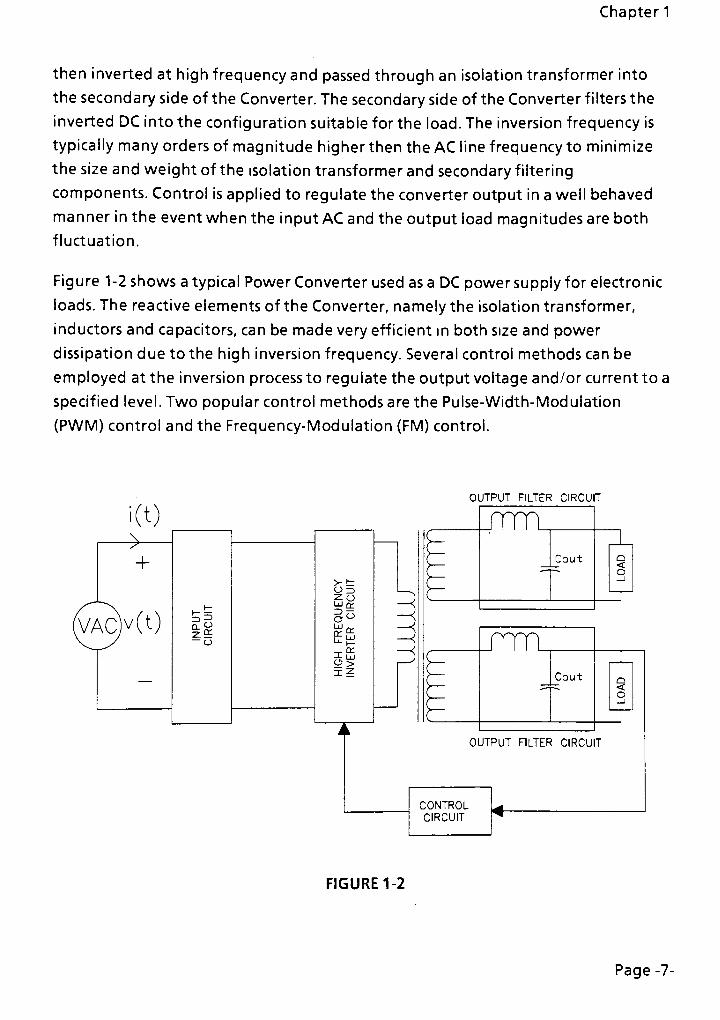
Figure 1-2 shows a typical Power Converter used as a DC power supply for electronic
loads. The reactive elements of the Converter, namely the isolation transformer,
inductors and capacitors, can be made very efficient in both size and power
dissipation due to the high inversion frequency. Several control methods can be
employed at the inversion process to regulate the output voltage and/or current to a
specified level. Two popular control methods are the Pulse-Width-Modulation
(PWM) control and the Frequency-Modulation (FM) control.
OUTPUT FILTER CIRCUIT
mm
Court
nm
Court
OUTPUT FILTER CIRCUIT
CONTROL
CIRCUIT
FIGURE 1-2
Page -7-

Chapter 1
Figure 1-3A illustrates a typical input circuit for the off line Power Converter. The
input AC is full wave rectified and feed to a smoothing capacitor. The AC is
converted into DC voltage across the capacitorwith only a small amount of AC ripple
superimposed at twice the AC line frequency. The high frequency inverter operates
from the capacitor voltage to produce the final output of the Power Converter.
Figure 1-3B is a slight modification of 1-3A to allow for switch modification for 120
or 240 Vrms input. When the switch is open the input is intended for 240 Vrms AC.
When the switch is closed, the input stage forms a voltage doubler to produce the
same DC voltage on the capacitor as the case for 1 20 Vrms AC.
Figure 1-4 displays typical voltage and current waveforms of the input circuit. The
voltage on the capacitor is charged to the peak value of the AC voltage.When the
AC amplitude is less then the voltage on the capacitor the bridge rectifiers are
reversed biased and the capacitor discharges due to the load demand of the
subsequent circuits. Consequently the current is drawn from the AC lines only for a
small duration of the AC cycle when the voltage on the capacitor is less then the
input AC voltage. This type of input circuit is referred to as capacitor input filter since
the capacitor is the primary filter element of the input circuit.
The voltage and current waveforms of the capacitor input filter circuit has significant
impact on the efficiency of the AC line to deliver power through the Converter.
Page -8-

Chapter 1
i(t)
+
(VAC)v(t)
r-
Dl
K~i
D2
B3
D4,<-^
CIN
>- tz
z 0u
eg
-r^
12
INPUT CIRCUIT
FIGURE 1-3A
i(t)^
r"
+
(VAC)v(t)
Dli'"I
D2
D3W-
D4
f*
120V
240V
CI
C2
CIN
. _l
z o
=5 r^o
Ow rv-
^
INPUT CIRCUIT
FIGURE 1-3B
Page -9-

Chapter 1
FIGURE 1-4
Page -10-

Chapter 1
The parameters of the current waveform that is of interest are:
The rms value of the current waveform at the fundamental frequency of the ACvoltage.
Total rms value of the current waveform at the harmonic frequencies of the AC
voltage.
Relative phase angle of the current and voltage waveform at the fundamental
frequency of the AC voltage.
The power delivered to the Power Converter by the AC lines is equal to the product
of the rms voltage and rms current values. This power is defined as the Apparent
Power input to the Converter (pA):
P=V IA rms rms
The one cycle average of the instantaneous product of the input AC voltage and
current is defined as the Real Power input to the Converter (pR):
PR= h \ v{t)i{t)dt
Where:
v(t) = AC line voltage
i(t) AC line current.
A figure of merit using the relative ratio of the real power over the apparent power
is the power factor of the Converter {pf):
PA
The power factor is maximized at unitywhen the real power and apparent power
are equal. The benefits in maximizing PF are summarized:
More power can be delivered through the Converter to the loads at the same AC
outlet rating:
Page -11-

Chapter 1
OutputPower=zV I PFrms rms
Where e = Efficiency of the Converter.
The available outlet power is maximized for output power for pf of unity.
In three phase with neutral AC supply configuration, lowering the harmonic
content of the AC current in each phase reduces the harmonic current that must be
carried by the neutral conductor.
Reducing the harmonic losses of the Utility line reactive elements such as
Transformers, Motors, Caoacitors, Reactors...
Reduce conducted and radiated electronic noise pollution.
To derive maximum power factor it is necessary to correct the distorted current
waveform of Figure 1-4. Methods to"shape"
the current waveform can be
categorized into passive Power Factor Correction {pfc) and active Power Factor
Correction. As the name implies, passive PFC uses passive elements in networks
which the current waveform is"shaped"
or filtered to remove the unwanted
harmonics. The passive PFC networks can be very effective in increasing the pf of the
capacitive input filter converters. However these passive PFC networks must operate
at the AC line frequencywhich dictates the bulky physical size and weight of the
passive elements. This disadvantage must be balanced against the appeal of the
relative simplicity of the passive pfc networks.
An alternative to passive PFC networks is to use active circuits to reshape the current
waveform. The active circuit consist of a power converter operating at frequencies
several orders of magnitude higher then the AC line frequency. The physical size and
weight of the reactive elements used in the active pfc converter is much reduced
compared to its counter parts in the passive pfc networks. The active pfc converter
can also achieve near unity pfwith very reasonable reactiveelement values. The
disadvantage of the active PFC Converter is it's relative complexity compared to the
passive PFC networks.
Page -12-

Chapter 1
The main thrust of this Thesis is focused on the analysis of active PFC Converters.
However for the purpose of comparison and completeness, two popular passive PFC
networks are analyzed and presented as well.
Page -13-

Chapter 2
CHAPTER 2
MATHEMATICAL DESCRIPTION
OF POWER FACTOR
2.1 POWER FACTOR FOR PURE SINUSOIDAL VOLTAGE AND CURRENT:
Power factor (pf), as generally applied to distortion free sinusoidal voltage and
current waveforms, describes the relationship between the apparent power
extracted from a driving source and the real power delivered to a receiving load. In
mathematical expression, pf is a ratio of the real power delivered to the load and
the apparent power supplied by the source:
PF=^- (2-1)
PA
where PR = Real Power and PA = Apparent Power.
Since power converters are typically operated by the Utility supplied power line, the
driving source is the alternating current (AC), 50 or 60HZ, sinusoidal voltage.
Let v(t) and i(t) represent the utility line voltage and current:
v(t) = a sindxtt) and i(t) = b sin((x>t) (2-2)
Where:
co = 2nf.
f= Utility line freq uency.
a = Voltage peak amplitude.
b = Current peak amplitude.
Real power is defined as the instantaneous product of the voltage and current
averaged over one line cycle:
l\T
p =-
v(t)i{t)dt (2-3)R T Jo
Page -14-

Chapter 2
The apparent power is defined as the product of the rms values of the voltage and
current:
p=v IA rms rms
(2-4)
Substituting (2-3) and (2-4) into (2-1):
PF
1
T
'T
v(t) i(t) dt
V Irms rms
(2-5)
Equation (2-5) is the basic mathematical definition of power factor.
For the casewhere the voltage and current waveforms are in phase and distortion
free sinusoids expressed by equation (2-2), the rms values are:
l
Tu(i)2dt
0.5
a
V2
1
T J
i(t)2
dt
0.5
b
V2
The apparent power expression:
ab
The real power as defined by (2-3):
ab
v(t) Hi) = a sin(03t) b sinfat) = ab sin (cor) -
1 cos(2(x>t)
Integrate over one line cycle:
0)
2n ,
r ab 1 -cos(2co<)w ab
dt-
2n 2
2nsin(4n)
CO
-
ab
2
Page -15-

Chapter 2
Using the expression forPA and P^, the power factor for in phase distortion free
sinusoidal voltage and currentwaveforms is equal to unity:
PF= = 1
pa
The unity power factor describes the case where the apparent power extracted from
the driving AC voltage source is equal to the real power delivered to the load.
Notice the voltage and current expressions of (2-2) are related by a scaler constant:
v(t) a
=-
=R
Ut) b
Where by definition, R = Resistance of the load.
When the load is not purely resistive but posses reactive elements, the current
extracted from the driving source will be phase shifted relative to the voltage:
v(t) = a sin(coi) and i(t) b sin(u>t+Q)
where 8 = phase angle between u(t) and i(t).
The real power delivered to the load is altered :
u(t) lit) ab siniut) sm(cot+ 9)
Expanding i(t):
i(t) = b sin{(x>t)eos(Q) + b cos((ot)sin(Q)
v(i) i(t) - ab sin2(a>t)cos(9) + sin((x>t)cos{ti)t)sin(Q)
The first term is further expanded :
a b sin (u>t)cos(Q) =-
a b2
1 -cos(2coi) cos(9)
Page -16-

Chapter 2
The second term is also further expanded:
a b sin{u>t)cos((x)t)sin(B) =-
sm(2cof)sin(9)
2
When both terms are integrated from 0 to 2n/co, the sin{2aat) term integrates to zero
and cos(O) cancels with cos(4n). The result is:
l
P =-
ab cos(9)H
2
The rms values of v(t) and i(t) were not changed by the phase shift, the apparent
power remains the same:
l
P=-abA 2
Finally, the power factor for phase shifted, distortion free sinusoidal voltage and
current waveforms is:
p
.-.
pf= = cosid) (2-6)
pa
Page-17-

Chapter 2
2.2 POWER FACTOR FOR DISTORTED SINUSOIDAL VOLTAGE AND
CURRENT:
A more general expression for PF can be derived with only v(t) is assumed to be
distortion free. The frequency component of v(t) is considered as the fundamental
frequency component of the system.
PF expression is first normalized about v(t):
PF =
1
T
Tb
v(t) i(t) dt cos(Q)
0 V2 V2
VI alrms rms rms
V2
Usingj- I = rms value ofthe i{t) component at the fundamental frequency of co.V z
-7-
I. cosiQ)V2 l
PF =
alrms
/
PF = cos(9) (2"7)/rms
Where:
7i = rms value of i(t) at the fundamental frequency cu.
9 = The phase angle between the fundamental component of at) and u<t>:
irms= Total rms value of i(t).
The power factor expression (2-7) indicates two contributing causes to the
degradation ofpf from unity:
The phase displacement of the fundamental frequency component of the current
with respect to the AC line voltage source.
The relative ratio of the rms value of the currentwaveform at the fundamental
frequency of the AC voltage to the total rms value of currentwaveform.
Page -18-

Chapter 2
The pf expression (2-7) now includes the phase shifted effect of linear reactive load
as well as the distortion effect of non-linear load.
Equation (2-7) can be further generalized to include the case when the voltage
source is also distorted. In real world situations where the Utility supply contains
non-zero source impedance, the voltage waveform will be corrupted by the
distorted current waveform. To generalize equation (2-7), both v(t) and i(t) are
assumed to posses frequency components at the harmonics of the fundamental
frequency co.
Let vn(t) and im(t) represent the nth and mth Fourier component of the voltage and
current respectively:
v it) = a sininat) and i (t) b sin(mcot)n m
(2-8)
Where n and m are integer numbers.
LetpftJ represent the product of vn(t) and im(t):
p(t) = v (t)i it) a b sininat) sinimat)r
n m
Expanding sin(neat)sin(mat):
l l
pit) =-
abcos[inm)(i>t]-
a b cos[in+ m)ozt]
2 2
Integrate pit) over one line cycle to yield real power:
CO 1,
P = abR 2n 2
1
R~
T
i
pit) dt
0
2n 2n
t
cos[ in m)u)t ] dt cos[ in+m)u>t] dt
i Jo 0
The first integral term inside the bracket:
Page -19-

Chapter 2
2n
co 1cos[ in-m)ut ] dt = sin[ in- m) 2n ] when n* m
'0 in-m)2u
2n
w 2ncos[ in- m)(at ]dt= when n= m
0 co
The second term integral term inside the bracket:
2n
cos[in+m)(ot]dt=sm[in+m)2u
0 in+m) 2n
Since n and m are integers and sine function evaluated at integer multiple of 2n are
always equal to zero, the first integral term inside the bracket for n* m and the
second integral term inside the bracket will always evaluate to zero. Therefore:
a b
2
and
PR-0whenn^m and PR= whenn=m (2-9)
PF = Qwhenn*m and PF -\whenn- m (2-10)
Equations (2-9) and (2-10) indicates only the frequency components of the current
that match those of the driving voltage source will deliver power from the source to
the load (n = m). Therefore any frequency component of the current not present in
the driving voltage source will not contribute to the power throughput to the load
(n^m).
However, the frequency component of the current not present in the driving voltage
source will still contribute to the total rms content of the current and consequently
to power lost in the parasitic impedances of the converter circuit. Therefore for a
particular total rms current magnitude, the maximum power is delivered to the load
onlywhen all of the Fourier component of the current are matched and in phase
with the Fourier component of the driving voltage source. Another word, maximum
power delivery occurs when all of the Fourier component of the current is related to
its matching voltage Fourier component by a scaler multiplier. The scaler multiplier,
Page -20-

Chapter 2
as previously described, is by definition the resistance of the load. Consequently pf is
at unity onlywhen the load seen by the driving source is purely resistive at all of its
Fourier component.
2.3 POWER FACTORAND TOTAL HARMONIC DISTORTION:
The Total Harmonic Distortion (thd) of the current i(t) is defined as the ratio of the
rms values of the harmonics over the rms value of the fundamental component:
0.5
THD =
II2
* n
71 = 2(2-11)
Where:
n = nth harmonic of i(t)
l\ rms value of the i(t) at the fundamental frequency co.
0.5
In = 2
total rms values ofthe harmonics ofiit)
Let ih = total rms values of the harmonic of i(t):
IH=
0.5
L
n = 2
2
arms
(2-12)
Rearrange equation (2-7) for 7i (since h is defined as a rms value, cos(Q) is set to 1):
i=pf I1 rms
(2-13)
/rms can be defined as the square root of the sum of the squares of the rms value of
i(t) at the fundamental frequency co and the total rms values of the harmonics of i(t):
0.5
Irms
i\+ X /;2
arms
n = 2
f +I2
1 h
10.5
(2-14)
Page -21

Chapter 2
Substituting equation (2-13) into equation (2-14) and solve for Iy.
h=
\.PF*
0.5(2-15)
Substituting equation (2-15) into equation (2-11):
THD - 1PF1
0.5
(2-16)
Using equations (2-7), (2-11) and (2-14) to solve for PF:
PF =
cosiB)
THD2+ 1
10.5 (2-17)
Where 6 = The phase angle between the fundamental component of i(t) and v(t).
Equations (2-16) and (2-17) indicates as pf approaches unity, thd will approach zero.
However, as THD approaches zero, the PFwill not approach unity. The pf becomes a
function of 0 as THD approaches zero.
Equation (2-16) is used to generate table 2-1 with 8 = 0. Table 2-1 examines power
factor versus total harmonic distortion as a percent of fundamental component.
From the data listed in table 2-1, with power factor <0.7, the total rms value of the
harmonics is actually greater then the rms value of the fundamental. It follows that
if power is only delivered to the load at the fundamental frequency of the driving
voltage source, assuming voltage is distortion free, the efficiency will be below 50%
for power factor <0.7. Also from table 2-1 ,power factor above 0.9992 is necessary if
THD below 4% is required.
Figure 2-1 is a plot of power factor versus total harmonic distortion generated from
equation (2-16).
Page -22-

Chapter 2
TABLE 2-1
Power Factor {pf) versus Total Harmonic Distortion (THD){6 = O.cosd = 1)
PF THDX100(%)
0.500 173.21%
0.600 133.33%
0.700 102.02%
0.800 75.00%
0.900 48.43%
0.950 32.87%
0.960 29.17%
0.970 25.06%
0.980 20.31%
0.990 14.25%
0.992 12.73%
0.994 11.00%
0.995 10.04%
0.996 8.97%
0.997 7.76%
0.998 6.33%
0.999 4.48%
0.9992 4.00%
0.9994 3.47%
0.9996 2.83%
0.9998 2.00%
0.9999 1.41%
1 .0000 0.00%
Page -23-

Chapter 2
FIGURE 2-1
Power Factor (pf) versus Total Harmonic Distortion (THD){6 = O.cosd = 1)
0.5 0.55 0.6 0.65
T
0.7 0.75 0.8
POWER FACTOR
0.85 0.9 0.95
Page -24-

Chapter 3
CHAPTER 3
PASSIVE POWER FACTOR CORRECTION
Passive power factor correction networks employs passive filters to"shape"
or filter
the input line current. Two popular passive PF correction filter networks are:
Inductive Input Filter.
Resonant Input Filter.
The governing equations and maximum achievable power factor for each network
are studied in this chapter.
3.1 INDUCTIVE INPUT FILTER:
The inductive input filter, depicted in Figure 3-1, differwith the capacitor input filter
by an additional inductor. The equivalent circuit of the filter is displayed in Figure 3-
2. The sinusoidal line source and the full bridge connected rectifiers are replaced by
an equivalent absolute value sinusoidal source for analysis.
Unlike the capacitor input filter, where the capacitor voltage charges to the peak
amplitude of the input voltage, the inductor input filter averages the full wave
rectified voltage, vr, over a period that is half the period of the line source, n/co. The
extent of PF correction achieved by the inductive input filter is a function of the
inductor value, L, and the output load of the filter, R. The inductor serve as the
energy storage element filling in the discontinuous sections of the current pulses
and resulting in a more continuous waveform. However, the inductive input filter
can not produce unity power factor since the inductor current will never become an
in phase sinusoidal waveform. This can be explained by considering an infinite
inductor as a constant current source regardless the amplitude of the input voltage.
Therefor ^ven with an infinite inductance the current waveform will not be related
to the applied voltage by a scaler constant.
The two modes of operation for the inductive input filter are Continuous
Conduction Mode (CCM) and Discontinuous Conduction Mode (DCM). As the
Page -25-

Chapter 3
inductor value is increased the conduction time of the input current increases. For a
particular load R, at some inductor value the input current will cease to cross zero
and become continuous. In the application of PFC network the inductive input filter
is almost always designed to operate in the CCM mode.
The output DC voltage across the capacitor can be derived by ignoring the AC ripple
voltage component and solve for the average voltage component. The assumption is
valid since for pfc application the time constant of the filter is much greater then the
time constant of the full wave rectified line frequency n/co.
Page 26-

i(t)
+
(VAC)v(t)
r"
Dl
?f
D2
D3
D4
*
rmrnnI
>
i(t)
CIN
INPUT CIRCUIT
FIGURE 3-1
Chapter 3
10
+
vo o<o
PEAK = a
nsnsn
(t)>
+
vr(t
mmm >
CIN
10
+
voR
EQUIVALENT INPUT CIRCUIT
FIGURE 3-2
Page -27-

Chapter 3
The input off line voltage v(t) once again is:
v(t) = a siniwt)
The full wave rectified voltage v/t) is:
v it) = a sinidot) (3-1)
The averaging effect of the inductive input filter on the full wave rectified voltage
ur(t) can be expressed as:
n
co to a
a sinicot) dt =
n J0 n
cosn + cosO
2a= = 0.6366a
n
(3-2)
The voltage across the inductor equals to the difference between the input voltage
Vr(t) and the capacitor voltage v0:
2a
vAt) = v it) - V - a siniat)- for 0 < at < n
L r Un
(3-3)
Using:
d i it)
vAt) =L
L dt
and integrating the inductor voltage to derive the inductor current:
lr.lt)=I JvAt)dt+ i.(0) = 7l L L
a siniat)
2a
dt + i (0)
Simplify:
^'ZL
2coL 2at
1 + cosiwt)
nR n(3-4)
Page -28-

Chapter 3
The rms value of the input current is solved from the expression for the inductor
current:
ilLrms
n
CO CO
n . 0 . coL
2coL 2cof1 H cosiat)
ni? n
dt
Expanding:
Sa'a
2k
24a 5a
Lrms+ +
co n R n 6 L co
Find the square root:
Lrms
8a 4a5a'
+ ^ +
0.5
L2co2n2 R2n2 6L2co2
5i?2n2
+ 24(L2co2
-
2i?2
0.5
6L2co2P2n2
4a" 5fl2n2
2P/
I24L2co2 L2co2
0.5
Finally:
2a f5#2n2
2P/0.5
*"ni?
l24L2co2 L2co2
+ 1(3-5)
A normalized load parameter constant of DC output resistance R versus the
inductive reactance of the inductive filter can be definedas:
R_coL
(3-6)
Page -29-

Equation (3-5) rewritten as a function of Q:
Chapter 3
2a 52 2
a52a
(,= Qn-2Q2+1 =
^^ni? 24
*
J nfl
Q'
n 224
, 0.5
+ 1 (3-7)
For convenience, define ka as:
k =\QZ
uA-2
24+ 1
0.5
The expression for the rms current is simplified :
2a
iT = kLrms ^ q (3-8)
The power factor as defined by equation (2-1) is:
PF=
PA
Since the output of the inductive input filter is assumed to be a pure DC, the input
real power is equal to the product of the output DC voltage and current (ignoring
DC losses within the filter):
4aP = V I =
R OlO 2pn R
(3-9)
The input apparent powerwas defined as the product of the rms values of input
voltage and current:
2a a
P.=i. V = k -7-
A Lrms rmsriR 9 V2 (3-10)
The power factor solved from the ratio of equations (3-9) and (3-10):
PF =
2V2 j_n k (3-11)
Page -30-

Chapter 3
Both kq and pf are functions of Q. Therefore as L approaches infinity and Q
approaches zero {kq approaches 1 ), the maximum PF obtainable by an inductive
input filter is:
PF2V2
= ~
0.9003 (3-12)MAXIMUM
7
Equation (3-4) rewritten as function of Q:
2 cor:
(3-13)
a 2 2wt1 + cos(coi)
nQ n
The Q value designate the onset of CCM, Qc, can be solved from equation (3-13) by
calculating the Q value required for il(V = 0:
In n-
=wt+ -cosiut)-
(3-14)
cof can be solved by differentiating equation (3-13) with respect to t and then set to
equal to 0:
diL{t)a 2a
= siniwt) = 0dt L nL
a 2a
sinioit) =
L nL
2
sini(i>t)
n
co*=
sin~l(-)==
39.54
(3-15)
Substituting equation (3-15) into equation (3-14):
Page -31-
Chapter 3
Q,sin
-1,
2X
\n
n /
+ -cos1
2sin
n
2
Qc-3
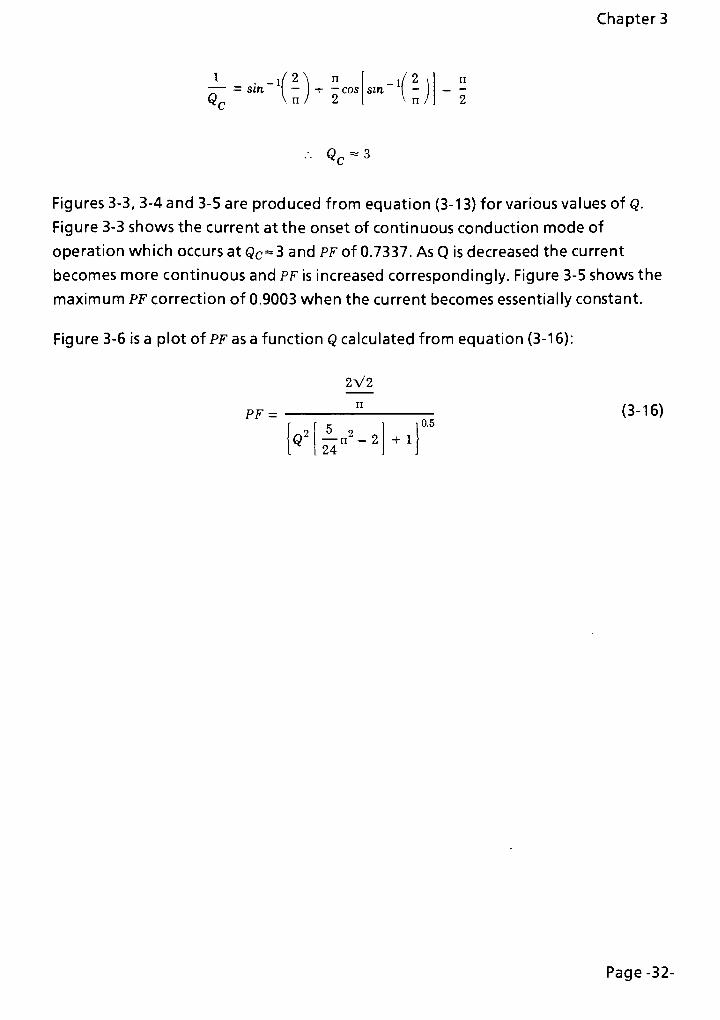
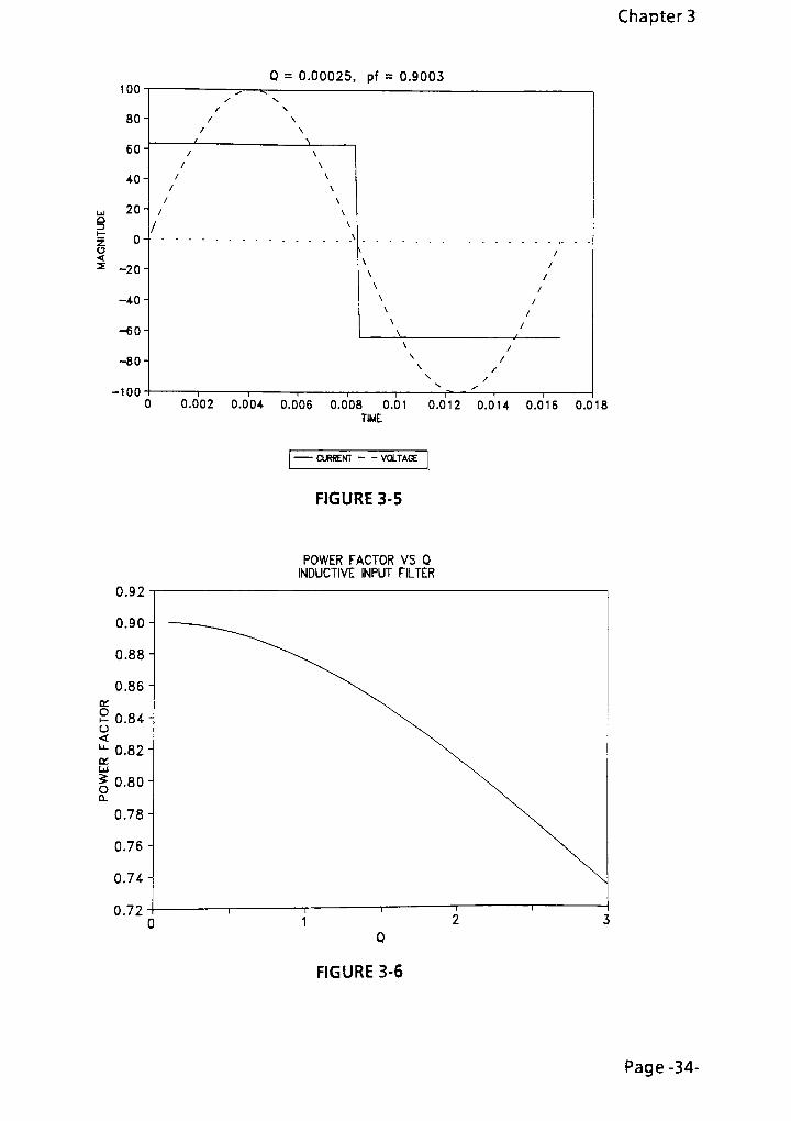
Figures 3-3, 3-4 and 3-5 are produced from equation (3-13) for various values of Q.
Figure 3-3 shows the current at the onset of continuous conduction mode of
operation which occurs at Qc=3 and PF of 0.7337. As Q is decreased the current
becomes more continuous and PF is increased correspondingly. Figure 3-5 shows the
maximum PF correction of 0.9003 when the current becomes essentially constant.
Figure 3-6 is a plot of PF as a function Q calculated from equation (3-1 6):
2V2
PF
Q' i- 29n I
24
,0.5
(3-16)
+ 1
Page -32-

Chapter 3
150
Q = 3. pf = 0.7337
0 0.002 0.004 0.006 0.008 0.01 0.012 0.014 0.016 0.018
TIME
CURRENT VOLTAGE
FIGURE 3-3
Q = 0.5, pf = 0.8941
0 0.002 0.004 0.006 0.008 0.01 0.012 0.014 0.016 0.0
TIME
18
CURRENT- - VOLTAGE
FIGURE 3-4
Page -33-
Chapter 3
Q = 0.00025, pf = 0.9003
100 -i
X
/ \
B0-/ \
/ \
' \60-
/ \
i \
40- i
i
i
\
uj20-
i \
Q
? o-
1 \
\
e> V
<3 -20-
\
\
/
/
/
-40-]\
\
/
/
-60-
\
\
/
\/
-80-
\
\/
/\
/
-100-
i 1 1 1 11=
s
0 0.002 0.004 0.006 0.008 0.01 0.012 0.014 0.016 0.0
TIME
18
CURRENT VOLTAGE
FIGURE 3-5
POWER FACTOR VS Q
INDUCTIVE INPUT FILTER
0.92
FIGURE 3-6
Page -34-

Chapter 3
3.2 RESONANT INPUT FILTER
The resonant input filter, displayed in Figure 3-7, inserts a series inductor/capacitor
filter between the input line and the rectifier bridge. The inductor/capacitor forms a
series resonant network which only allows current to pass at the resonant frequency
of the filter. At the resonant frequency of the filter the inductive reactance exactly
cancels the capacitive reactance and results in maximum current flowing through
the bridge rectifiers.When the resonant frequency of the filter is tuned to the line
frequency, only line frequency current component is allowed to pass through the
filter. For the ideal case of zero DC resistance, the input current can be shaped into a
sinusoidal waveform and resulting in power factor of unity.
The resonant input filter is defined by it's resonant frequency wr and it's
characteristic impedance ZR:
1(L^5
coR
j^0.5
R \ CLC
The resonant frequency of the filter is tuned to the frequency of the input line to
obtain maximum power factor:
"r
The AC ripple component across the bulk storage capacitor is again ignored. The DC
output voltage across the storage capacitor will produce a DC current in the load
resistance modeled by R. In the equivalent circuit of the resonantfilter displayed in
Figure 3-8 the effect of the bridge rectifier and the DC output voltage is modeled by
the square wave alternating between themagnitudes +v0 and -v0 at the load side
of the filter. Representing the alternatingamplitude square wave by Fourier Series:
v0it) =
4V0 sini3wt) sini5a>t)
siniut) -I +" +
The input voltage to the resonant input filteris the AC line voltage:
v(t) - a sinioit)
Page 35

Chapter 3
The inductive reactance and capacitive reactance cancels at the line frequency co.
With no DC resistance assumed in the filter, the net voltage drop across the filter
must then be zero at co. This condition is satisfied when the frequency component of
the input voltage at co exhibits equal magnitude compared to the frequency
component of the output voltage at co.
With the input voltage magnitude at frequency co equal to a and the output voltage
magnitude at frequency co given by the fundamental term in the Fourier Series:
a=2. (3-17)n
After rearranging:
a n
vo=T (3-18)
During the interval 0 ^ t < n/co, the KVL equation for the equivalent circuit of Figure
3-8 is:
vit)-
vLit)- vcit) - VQ
= 0 (3-19)
Where:
diAt)
vAt) = L (3-20)L dt
^=C)iit)dt (3.21)
Since the inductor and capacitor are series connected:
iLit)=icit)
Substituting the expression for v(t) andequations (3-20), (3-21) into equation (3-19):
Page -36-

Chapter 3
a sm(cot) L
diLit)
dt
1
C icit)dt-VQ= 0 (3-22)
Differentiating both side of equation (3-22) to eliminate the integral operator:
d
i
acocos(cot) L iAt) iAt) = 0dt2 L C L
(3-23)
During the interval 0< t < n/co, v0 is a DC voltage which differentiates to zero.
Solving equation (3-23) for iut) using LaPlace Transform.
Converting equation (3-23) to LaPlace Transform:
aco
c?2 ,2
& + co
- L SILiS)-SILiO)-iLiO)c
Where IL(0) is the initial value for iL(t) and iL'(0) is the initial value for the
differentiation of iL(t).
Collecting terms and solving foriLes;:
r {S) =-
;+ iLiO)
-^--
+ iL'iO)-yi-
.,
L L (S2
+S2
+S2
+co2
By definition:
2_
CO =
LC
Taking the inverse LaPlaceTransform to derive iL(t)
it
iLiO)
i (t) = sm(coi) + iLiO)cosi(t) + sin(cot)
A> 2L w
Page -37-

Chapter 3
iL(0) denotes the initial condition of the inductor current. Considering the inductor
current is in series with the input current, non-zero initial current condition is not
allowed. Therefore iL(0) is set to zero.
The inductor current expression becomes:
.
,at
lL(0)
irU) = sini(x>t) + sin(coi)L 2L co
(3-24)
The term for iL'(0) can be derived by equating the output DC current i0 to the
average current in the inductor. During the interval 0 < t < n/co:
iTii)dt =1 =
n 0L R
(3-25)
Substituting equation (3-24) into equation (3-25):
CO
n
co at co
sinicot) dt +
0 2L n
n >
-
iAO)co L
0
sm(co<) d( = IO
Solving the integral terms:
a
i
2 ^(0)
_
VQ
2coL co P
(3-26)
Rearrange foriL'(0)'
VOwnan
(3-27)
Substituting equation (3-27) into equation (3-24):
atVOn
an.
j ) = sin(cof) +-
siri(corO- sin(cofl
LK
2L 2R 4coL
(3-28)
Page -38

Using:
ZR= o>L
Chapter 3
atOn
anirit)=
sin(coi) -I siniat) - strt(cof)2i? 4ZD2L
(3-29)
Substitute the expression:
an
into equation (3-29):
at ann an
irit) sinicat) + siniwt) siniatt)L 2L 8P 4ZD
(3-30)
Rearrange:
ncoLa\ZRt
n
iTit) = sin(cor) HL 2Za\ L 2 [ 2R
- i siniat) (3-31)
Substituting the load parameters Q of equation (3-6) into equation (3-31):
a f ZR*
n
iT it) - siniwt) +
-
L
2ZR [ L 2
n
2Q~l
sm(cort)(3-32)
Equation (3-32) is the expression for the input current of the resonant input filter.
The average input current can be solved by integrating equation (3-32) over the
interval 0 < t < n/co:
to
Aug~
n
co a\ZRl
.
, sn
sini(x>t) +
0 2ZR\ L 2
n
2Q_1 siniu>t) \ dt =
a n
4ZRQ
(3-33)
Solving for the rms expression of the input current:
Page -39-

Chapter 3
. 2 w
rnzsn
n
co | a
o liz]sin(cot) H
I L 2 2Q
- 1 stn(cof) ) } dt
2 49 an
r =
rms. 2 ^.2
2 2 2an a
+
128Z^Q"
96Z2
16Z2
(3-34)
Factor out:
2 2a n
and2Z2 32
H
From equation (3-34) and solve for the square root:
a n
rms2ZD 4V2
1 4 8
Q2
3 J
0.5
(3-35)
The input real power is equal to the product of the output DC voltage and current:
an an
Pr,= VI=R 00 4 4ZDQ
(3-36)
The input apparent power is equal to the product of the rms values of input voltage
and current:
a a n
P = V IA rms rms V2 2 Z 4V 2
R.
/n2 0 2 4
Q 3 n n
0.5
(3-37)
The power factor as the ratio of real power and apparent power can now be solved
from equations (3-36) and (3-37):
PF=^
PA
1
Q
1_4_ 8_
Q2
3
0.5(3-38)
Page -40-

Chapter 3
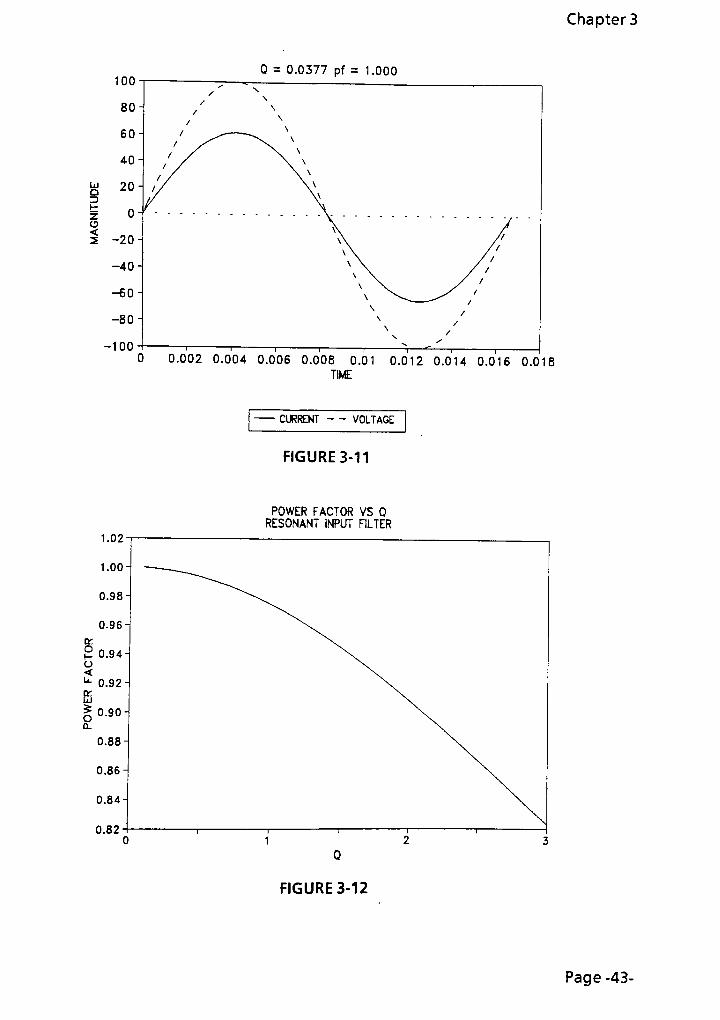
Figures 3-9, 3-10 and 3-11 are produced from equation (3-32) for various values of Q.
Figure 3-9 shows the current at the onset of continuous conduction mode which
occurs at Q = 1 .58 and pf of 0.94. As Q is decreased the power factor increases
correspondingly until maximum power factor of unity is reached in Figure 3-11.
Figure 3-9, 3-10 and 3-11 illustrates the degradation ofpf is attributed primarily to
phase displacement since the current distortion is relatively low, especially compared
to the current waveform of the Inductive input filter.
Figure 3-1 2 is a plot of pf as a function Q calculated from equation (3-38).
Page -41

i(t)r"
+
(VAC)v(t)
mmm->
iL(t)
Dl
D2
D3
D4,
Chapter 3
W-T 1
i 10
CIN
INPUT CIRCUIT
FIGURE 3-7
+
VO D<
O
mrmy c|(
L
i(t)+vo
-vol
EQUIVALENT INPUT CIRCUIT
FIGURE 3-8

Chapter 3
Q = 1.58 pf = 0.94
0 0.002 0.004 0.006 0.008 0.0! 0.012 0.014 0.016 0.01
TIME
CURRENT - - VOLTAGE
FIGURE 3-9
Q = 0.942 pf = 0.9773
0 0 002 0.004 0.006 0.008 0.01 0.012 0.014 0.016 0.018
TIME
CURRENT- - VOLTAGE
FIGURE 3-10
Page -42-
Chapter 3
Q = 0.0377 pf = 1.000
0.002 0.004 0.006 0.008 0.01 0.012 0.014 0,016 0.018
TIME
CURRENT - -
VOLTAGE
FIGURE 3-11
POWER FACTOR VS QRESONANT INPUT FILTER
FIGURE 3-12
Page -43-

Chapter 4
CHAPTER 4
ACTIVE POWER FACTOR CORRECTION
4.1 ACTIVE POWER FACTOR CORRECTION CONVERTERS:
Besides using passive networks, active power conversion circuits can be employed as
PF correction converters. Passive pf correction networks filter and shape the current
waveform to remove the unwanted harmonics. The active pfc converter accomplish
the same by modulating the current extracted from the power line at the switching
frequency of the converter. The converter is placed between the capacitive input
filter and the power line to shape the line current into a more desirable waveform.
Compared to the passive pfc networks, the pfc converter can achieve the same or
higher PFwith much lower inductance value. The consequence of high frequency
input current modulation effectively multiplies the actual inductor value in the
convertor reflected into the AC line.
Of the four switching converter topologies, the Boost Converter is most used as pfc
converter. However all four switching converter topology can be designed to extent
control over its average input currentwaveform. Comparing the four topologies,
the Buck Converter has the disadvantage of requiring an additional input filter to
remove the switching frequency component from its pulsating input current.
However since typically the switching frequency is many orders of magnitude higher
then the AC line frequency, the requirement of the additional input filter is still
much reduced when compared to the passive networks discussed in Chapter 3.
When operating in the continuous inductor current mode, the input current
waveforms for the Boost, Buck-Boost and Cuk converters are non-pulsating.
Therefore, unlike the Buck Converter, an additional filter is not needed to smooth
the switching frequency component for the Boost, Buck-Boost and Cuk converters.
The Buck-Boost or Flyback Converter is mostly use in low power applications and is
not well suited for high power applications where PF correction is most needed and
used. For the Cuk converter, the stringent requirement for the series energy
transferring capacitor at high power applicationsmakes it undesirable.
Page -44-

Chapter 4
A conventional Boost Converter is displayed in Figure 4-1 . The transistor switch Q is
driven by a quasi-square wave with duty cycle 8. The switch is on during the interval
Srs and is off during the interval (l-8)rs. Ts is the period of the transistor switchingfrequency. When operating in continuous inductor current mode, the two
topologies of the Boost Converter during the two switching intervals is displayed in
Figures 4-2 and 4-3.
RL iL(t)L
>_mmm
+
D
Q
Vicft
c
Re
+
:vcft
10
+
VOR
BOOST CONVERTER
FIGURE 4-1
Page -45-

Chapter 4
RL
+
vs(t)
iL(t)L
^_jyrrm
\/
c
ic(t)
Re
+
vc(t)
10
+
VOR
RL
+
vsft
EQUIVALENT CIRCUIT FOR INTERVAL DTs
FIGURE 4-2
iL(t)L
/ mum\/icft
c 4=
Re
+
:vc(t
EQUIVALENT CIRCUIT FOR INTERVAL DTS
FIGURE 4-3
10
+
voR
Page -46-

Chapter 4
4.2 STATE-SPACE ANALYSIS:
Each circuit topology of the Boost Converter can be described by a set of state
equations. The current in the input inductor and the voltage across the output
capacitor are conveniently chosen as state variables. The state equations are written
in the form:
dx (4-1)= ax + bu
dt
y- ex (4-2)
Where x is the state variable, u is the input to the converter and a, b, and c are
constants.
The two sets of state equations, one for the interval Srs and one for the interval (l-
8)TS, are combined to generate a single set of state equation describing the Boost
Convert for the entire switching period Ts-
Forthe circuit in Figure 4-2, the KVL equation around the input loop is:
di
VQ-iTR-L =0
Solving for the inductor current differential:
di. RT
i
-
=-
i, +-
Vs (4-3)dt L L L s
Forthe circuit in Figure 4-2, the KVL equation around the output loop is:
vc-Iovo +lcRc
=
Solving forthe capacitor voltage differential by using thefollowing:
dvcI0=-ic and ic
= C
Page -47-

Chapter 4
dV.
dtCiR0 + Rc)
Vr (4-4)
The output voltage v0 is related to the capacitor voltage Vc by:
R,
V = V0
C^R+R,(4-5)
Equations (4-3), (4-4) and (4-5) are the state equations for the Boost Converter
during the interval Srs. Notice equations (4-3) and (4-4) conforms to equation (4-1)
and equation (4-5) conforms to equation (4-2).
For the circuit in Figure 4-3, the KVL equation around the input loop is:
vc + lcRc-IoRo=
Using i0 = iL-ic;
VC +iCRC-[lL-iC R0
=
Once again, solving forthe capacitor voltage differential:
dt
R,
CiR0 + Rc: ClRQ + Rc)(4-6)
Forthe circuit in Figure 4-3, the KVL equation around the output loop is:
VS-lLRL-Lir-lCRC-VC=
Substituting for ;cand using equation (4-6) as the expression for the voltage
differential and then solve for the inductor current differential:
di^dt
i?L*(P0i|Pc)
lL~
R,
LiR0 + Rc)\ *A(4-7)
Page -48-

Where:
Chapter 4
RoRcRJRr =0 c R + R
O C
The expression for v0 is:
vo=
vc + icRc
Substituting for ic and using equation (4-6) for capacitor voltage differential and
solve for v0:
V0=iRO^C]lL +
R,
iR0 + Rc:(4-8)
Equations (4-6), (4-7) and (4-8) are the state equations for the Boost Converter
during the interval (1-8)PS. Notice equations (4-6) and (4-7) conforms to equation (4-
1) and equation (4-8) conforms to equation (4-2).
Combining equations (4-3) and (4-4) into a single matrix equation in the form of:
dx
dtA x + b u
dlL ~RL0
dt 1-f
L
dvrJ"
'[ -1 1 i
dt
u
CiRo+ Rc)
v
1
+ \l0
vr(4-9)
Similarly, equations (4-6) and (4-7) can also be combined into a single matrix
equation in the form of:
dx
-=V+ b2u
Page -49-

Chapter 4
diL RL + (.R0\\RC)~R0
lL
[vc1-
1
L
0
dt
1=(dvc I I
L
R0
LiRQ + Rc)
J-1
dtCiR0+Rc) CiRQ + Rc)
(4-10)
V,
The two state matrix equations of (4-9) and (4-10) describes the Boost Converter
during the intervals Srs and (1-8)TS. A single state matrix equation can now be
derived to describe the Boost Converter over the entire switching period Ts by
combining equations (4-9) and (4-10) afterweighting each equation by their
respective duty cycle:
^=8( Alx-!-b)u) hG'(A2, : b,;u (4-11)
Where8'
= 1-8.
Expanding equation (4-11):
dx= 8 A, x + 8b, u + 8'A.x + 8'bu
dt 1 l 2 2
Collecting like terms:
dx
dt=(8At
+ 8,A)x + (8b1 + 5'b2ju
Substituting:
A =
8A1 + 8'A2 and b =
8bj + 8'b2
dx= Ax + bu
dt(4-12)
Where the matrix constants A and b are:
Page -50-

RL + b-'iR0\\Rc. -8'R
o
L
8'R,
LiR0 + Rc)
-1
CiRQ+ Rc) C(RQ + RC
Chapter 4
b= \L
o
Following similar steps, equations (4-5) and (4-8) can also be averaged and combined
into a single equation. Using matrix notation, equations (4-5) and (4-8) can be
expressed:
y= C, x for interval 5T
J1 1 o
y= Cx for interval 8TC
Z L o
Combining the two equations:
y= 8C,x + 8'C_x
J 1 2
Using:
C =
8CX +8'C2
y= Cx (4-13)
The matrix constant C is:
R,
C= o'iRJR
0 C R + Rn0 C
A set of state equations has been derived to describethe BoostConverter over the
entire switching period Ts-
Page -51
Chapter 4
4.3 LARGE SIGNAL ANALYSIS:
Large signal analysis is necessary to derive the behavior of the Boost Converter
suitable for analysis interval of the 60HZ AC line.
By definition, for large signal analysis the state variables are at steady state value.
Setting the time varying variables of equation (4-12) to zero.
dx
dt
= Ax + b u (4-12)
Where:
dx
=0, 8 = D,8'= 1 -8 = 1 -D =
D'
dt
Substituting into equation (4-12):
0 = Ax + bu (4-14)
Solving forx:
x = A_1(-b)u(4-15)
Where the matrix constants and -b are
-i
D'R,
CiR0 + Rc) L(RQ + RC)
-D'R
0 RL + DAR0\\RC)
-l
CiR0+ Rc)
AD'
)
-b
-1
L
0
Page -52-

Chapter 4
and:
f{m =
rl(ro + rc) + d^rorc) + d'2r2o
LCiR0 +Rc)2
An expression for iL(t) can be extracted from equation (4-1 5):
~
LC(R, +flJ2
LdR0 + Rc) Q C
iAt) = u
RLiR0 + Rc) + D'iR0Rc) + D'2R2Q
After simplification:
iRn + Rr)uiAt) =
- - (4-16)
rl{Ro + rc) + d'{Rorc) + d Ro
In the application as a pfc converter, the input to the Boost Converter is the fullwave
rectified AC line voltage. In Figure 4-4, a Boost Converter is connected between the
AC line source and the energy storage, bulk DC filter capacitor. Figure 4-5 is the
equivalent circuit used for analysis.
Page -53-

Chapter 4
RL iL(t)L
D2w-+
vs(t)
D
D3
*
1
D4i
V
c ^k
ic(t
Re
+
Vc(t
10
+
VO<
o
BOOST POWER FACTOR CORRECTION (PFC) CONVERTER
FIGURE 4-4
+
\vs(t)
RL iL(t)L
D
\/ic(t
Re
C
+
vc
10
+
VO<
o
BOOST POWER FACTOR CORRECTION (PFC) CONVERTER
FIGURE 4-5
Page -54-

The input voltage source, u, is expressed as:
Chapter 4
u= V sinioit)
(4-17)
Using equation (4-17) as the input u for equation (4-16):
(R0 + Rc)vg sin(cort
i At) =
RTiRn + Rr,) +D'iRRr,) + D'2RlO O
(4-18)
Recalling from previous discussions (Chapter 2), maximum power factor of unity is
achieved when the voltage and current sinusoidal function is related by a scaler. For
a purely resistive load, the scaler is the resistance of the load. Examining equation(4-
18), the inductor current is a function of the termD'
in the denominator. The
inductor current waveform, hence the input current extracted from the line source,
can be controlled or"shaped"
by modulating the denominator term. To achieve
power factor correction, the denominator term is made to emulate a scaler term in
the form of an effective resistance:
p:
REff=
RL +D'(R0^ + D7i
(4-19)
(R0 + Rc)
The input terminals of the Boost Converter appears to be a resistive load to the line
source. The inductor current, hence the input current, is shaped by the effective
resistance REff-
sinioit)
W=-
R(4-20)
Eff
From the matrix equation (4-15), the large signal expression for the capacitor
voltage v^t) is:
Page -55-

Chapter 4
-D'Ro u
CiRn + Rr) L
VM) = - -
cfiD')
Vcit)D'R0iR0 + Rc)u
RLiR0 + Rc) + D'iR0Rc) + D'2R20
Which simplifies to:
Vcit) = D'R0iLit) (4-21)
The large signal input to output relationship of the Boost Converter is derived by
using the state equations (4-13) and (4-15):
The output state equation:
y= Cx (4-13)
For large signal analysis, set y = v0-
R
Vo=D^RJRc)lLit)+iI-f--Vcit) (4-22)
Substituting equation (4-21) into (4-22):
VQ= D'ILit)
R0 + R0RC
Ro + Rc
(4-23)
The large signal input to output relationship is derived by substituting state
equation (4-1 5) into state equation (4-1 3):
A_1(-b)u(4-15)
Substituting:
Page -56-

Chapter 4
y= CA"1(-b)u
Yields the Input to output equation:
-=CA_1(-b) (4-24)
Using the equation forthe vector C:
f RoC = D'ffljlff) +
0 C
<o+ >V
1and also using y
= v0, u = Vs and the equations for and -b
^=D'^- (4-25)V RS Eff
Equation (4-25) can be rearranged into a more common form:
yr>'2
_ ID'
R (4-26)
VS'
REff
With ideal components, the parasitic RL = RC = 0, the equation (4-26) is simplified:
-2
=1 (4-27)
VsD'
Page -57-

Chapter 4
4.4 DERIVING SINUSOIDAL AVERAGE INDUCTOR CURRENT:
Using equation (4-27), a large signal expression for duty cycle necessary to derive a
sinusoidal average inductor current can be estimated:
v
D = 1 siniat)
V0
Since the ratio of vg and Vo is constant, the large signal duty cycle expression
becomes:
v
D = 1 - K^iniut) whereK1= (4-28)
vo
Equation (4-28) is a generic duty cycle control expression, as a function of cof,
necessary to derive sinusoidal average inductor current for power factor correction.
It is based on the state space average analysis of the Boost Converterwhere the state
variables are averaged over the switching period. The expression forD hence are
valid only when averaged control function is implemented.
A significant amount of current distortion occurs near the zero crossing of the input
voltage waveform vs. The transistor switch is turned ON until the sensed average
current through the inductor reach the desired reference value. Referring to figure
4-3 and substituting the equation for vs into the KVL equation around the input
loop:
V siniwt) = Ucot)P. +L
diAut)
S L L dt
Rearranging:
diL(co<) v RL= sm(coi)
- t.(coi)r I L
dt L
Solve for iL(wt) by integrating both sides:
Page -58-

Chapter 4
t dJL(coy)
0 dt-dY =
{tV rtRg I
sm(coY) dx -
L(coY)dY0 ^ J o L L
(4-29)
Substituting equation (4-20) into equation (4-29):
tv
i (cofl = -5
sm(coY) dY -
sm(coY) dyJ o L J r rqLR
Eff
g
coL
1 cos(co<)
P. V
coLP
Eff
1 cx)s(cofl (4-30)
Simplify equation (4-30):
V"
iTiu>t) = S-L
coL
1 cos(cof)
p.
1 -
pEff
(4-31)
Solving equation (4-31) for the value of ujf when iL(cot) reaches the desired iLfco*)
expressed by equation (4-20):
V"
v
siniat)
REff <L
1 cosicot)
R,
1 -
pEff
Rearrange and simplify:
1 cosioit) g wL Eff coL
siniwt) Rff Vg REff-RL REff~RL(4-32)
Using the Trig identity to simplify equation (4-32):
9 1 - cos(6) siniQ)
tani~) = =
2 siniB) 1 + cosiB)
(dt coL
tani ) =
2 REff~
RL
Page -59-

Chapter 4
The value of at satisfying the the above equation will manifest as a lag in the
inductor current waveform relative to the input voltage. The current waveform
appear to be delayed while approaching the reference waveform.
Let y represent the delay angle of the inductor current:
(at (x>L
tani ) = tan(Y) = (4-33)2
REff~
RL
Solving the delay angle y as a function of P and Q:
Where: R = R - R Q=
bif Lco L
1
torc(y) =~
Q
y= tan-\-) (4-34)
Q
Figure 4-6 displays a plot of equation (4-34) where the delay angle is plotted over
three decade change in Q.
Page -60-

Chapter 4
FIGURE 4-6
The existence of the delay angle Ycan be physically explained by the inability of the
average inductor current to follow the input voltage near the zero crossings of the
voltage waveform. The rate of change of the input voltage is at maximum at the
zero crossing of the input voltage. The current in the inductor can not change as
rapidly as dictated by the input voltage at the zero crossings. The time constant of
the inductor, which is a function of the inductance and the effective impedance in
the circuit, constraints the ability of the inductor current to follow the voltage
waveform. The delay angle y is the result of the finite rate of change of the inductor
current and it is proportional to the relative dominance of the inductive time
constant of the converter. Using Q as a measure of the inductive time constant,
figure 4-6 shows as Q is increased, representing a decrease in the relative inductive
time constant, the delay angle Y falls off precipitously.
The existence and the explanation of the delay angle y is consistent with the known
fact in a purely inductive circuit, the current will lag behind the voltage by 90. A
Page -61-

Chapter 4
small Q means coL is much larger then the load P indicates the converter is relatively
inductive and the current lag is represented by Y. As Q is increased, the converter
becomes relatively resistive, the voltage and current becomes more in-phase, and
the delay angle decreases.
Page -62-

Chapter 4
4.5 DUTY CYCLE CONTROL FUNCTION:
The voltage across the inductor during the interval DTS is:
d i (cot)
= V sin(at) L(co()P.dt S L L
The voltage across the inductor during the interval D'TS is:
d i (cot)
= V siniat) - iAat)RT - Vdt 8 L L O
The average voltage voltage over the switching interval Ts is:
V siniat)- iAat)RT
g L L DTS + V siniat) - iAat)Rr - V_g L L U
D'Ts=VLiat)
After simplification:
VAat) = V siniat)- iAat)R. -
D'
VnL, g L, L, U
(4-35)
Using the desired averaged iL(cot) expression:
vg
i (cort = siniat)
REff(4-20)
The averaged voltage across the inductor can also be expressed as:
d iAat)
V
Rsiniat)
dt
= LEff
V coL
8
dt Rcosiat)
Eff
(4-36)
Equating (4-36) to (4-35) then substitute again (4-20):
V aL V
cosiat) = V siniat)-
-
siniat)-
D'
V
R g RrnnEff Eff
Page -63-

Solve forD'
vg v1 v
mLD'=
siniat) --^ -
siniat)R. -
cos(cof)
Collecting like terms:
Chapter 4
D'
=
, *ff~
RL \ ,co L
sm(coi) ( -
cosiat) \REff
REff
(4-37)
Equation (4-37) can be further simplified by using equations (4-33) and (4-38):
at co L sin(\)
tan( ) = tan(y) =
2^E/r
"
flL cos(y)
cos(Y)
P Pr = aL/F L
sm(y)(4-38)
Equation (4-37) becomes:
v
V0siniat)
aL \ / cos(y)
R I \ sin(y)
cosiat)
aL
REff
V aL
V0REff
,cos(Y) \
sinfcort ( - costcort
sin(y) /
V coL ,
8L
V0REff Sin(V} [siniat) cos(y)
- cosiat) sirc(y)
Using Trig identity to simplify the bracketedterm:
siniat) cos(y)- cosiat) sini\)
- siniat - y)
Page -64-

Chapter 4
D'
=
V aL siniat y)
V0REffsin(^(4-39)
Or:
D = 1 -
V aL siniat y)
V0REffsiniX)(4-40)
Equations (4-39) and (4-40) are valid for 0 <D'< 1 . Therefore:
V aL
g
V0REffsin(Y)
< 1
Notice sin(at-Y) is < Ofor at-Y < 0. Since it is by definition invalid forD'
to be < 0,D'
must then be constrained to 0 for small at values. This is precisely the condition
described by equation (4-33). During the lag angle interval, the actual current in the
inductor is below the desired sinusoidal current. The duty cycle control function for
the Boost Converter will attempt to correct for the lag angle by setting the duty cycle
to 1 until the average inductor current reaches the desired value at at = 2y.
Summarizing:
iLiat) =
g
co L
1 COSiUlt)
Eff
for 0 ut < 2y
(4-41)
sin(ut) for 2y < <j(< n
Eff
Equation (4-41) is used to calculate the desired and actual inductor current. The
value of at = 2y = 0.5 is exaggerated to show the distortion of the current when cut
becomes small. The magnitude of the current is normalized to 1 andthecoc scale is in
radian degree. Typical values of Q in an actual converter will not generate such
dramatic distortion unless the converter is very lightly loaded. Comparing to the
passive PFC networks where smaller Q will provide higher PF, the active pfc Boost
Converter actually degrades the PFfor small Q values due to the delay angle
distortions. Therefore there exist a lower bound for Q value in an active PFC Boost
Converter for a minimum acceptable PF.
Page -65-

Chapter 4
Diat) =
1 for 0 < wt < 2y
V co Lsirclcot- y>
18
V0REffsin(v)for 2y to* S n
(4-42)
Figure 4-8 display the duty cycle control function, calculated from equation (4-42)
and overlaid with the full wave rectified input voltage. The effect of the delay angle
is apparent. As at falls off below the delay angle region, the duty cycle is maintained
at 100% to maximize the average inductor current. Notice the inverse peak of the
duty cycle function is lagging behind the input voltage peak.
Page -66-
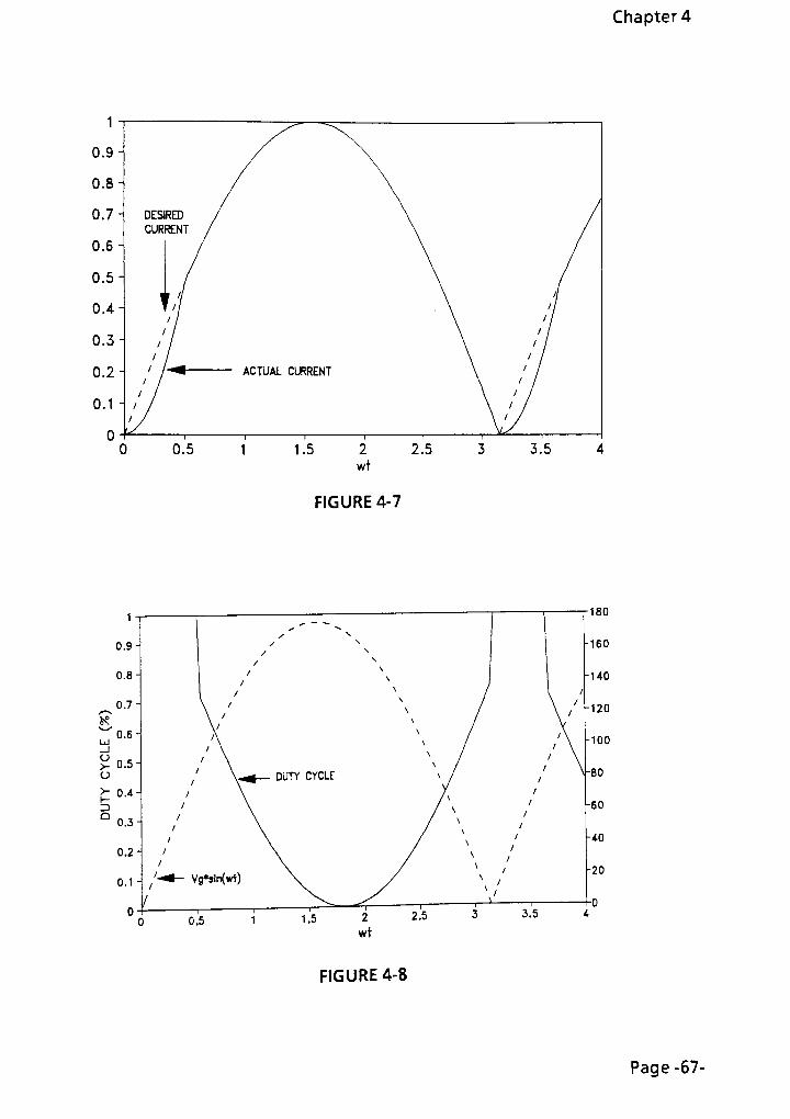
Chapter 4
FIGURE 4-7
FIGURE 4-8
Page -67-

Chapter 4
4.6 CONTROL FUNCTION IMPLEMENTATION:
The current waveform described by equation (4-41) is generated by the Boost
Converter when the duty cycle control function of equation (4-42) is implemented.
The dependent variables iL(at) and D(at) is referenced to the independent variables
Vs(at) where Vs(at) = vgsin(at). The functional diagram of such PFC Boost
Converter is displayed in Figure 4-9.
The current modulator control circuit of Figure 4-9 modulates the duty cycle
according to equation (4-42) to derive the averaged inductor current to follow the
input voltage reference. Two methods of implementing the current modulator
control function are displayed in Figure 4-10 and 4-11.
The current modulator control circuit of Figure 4-10 senses the inductor current and
compare it to a reference value iRef. The duty cycle is terminated when the peak
value of the inductor current reaches the value iRef. A negative compensation ramp
mc is added to the current reference to avoid subharmonic instabilitywhen the duty
cycle exceeds 50%. The duty cycle expression within the current modulator control
circuit can be derived as a function of the parameters displayed in Figure 4-10.
The current modulator control circuit of Figure 4-1 1 modulates the duty cycle as a
function of the averaged inductor current. The sensed inductor current is first
averaged then compared to the current reference iRef. The error amplifier output is
compared against a saw tooth signal to produce the duty cycle modulated
waveform.
Page -68-

Chapter 4
+
\vs(t
RL iL(t)L
e-v^^-irmm
SENSE
>
>
CURRENT
MODULATOR
CONTROLLER
d(t)
V SENSE
Q
\/ic(t
c 4=
Re
+
vcft
10
4-
VOQ
<
O
BOOST PFC WITH CURRENT MODULATOR CONTROLLER
FIGURE 4-9
Page -69-

PWM COMPARATOR
iL(0 5* K
0 ^j DRIVER >
RAMP COMPENSATION
^^c
:lock I
AVERAGE iL(0 = IL(t) x
FIGURE 4-10
-^ k;
Rz
R,[^
-VW^-Cf
; il(i)
PWM COMPARATOR
-> DR'VER : >
AVERAGE iL(t) = iL(t)
Vso*
FIGURE 4-11
Chapter 4
Page -70-

Chapter 4
4.7 DUTY CYCLE FUNCTION FOR AVERAGE INDUCTOR CURRENT
CONTROL:
The output of the PWM comparator will go high whenever the error signal, derived
by comparing the averaged inductor current to the current reference signal iRef,
exceeds the saw tooth signal. The duty cycle expression is the ratio of the averaged
error signal, il, and the saw tooth signal amplitude:
LetVs = peak amplitude of the saw tooth signal, then:
Saw
In the steady state condition where 8 = D:
D = (4-43)
Saw
4.8 DUTY CYCLE FUNCTION FOR PEAK INDUCTOR CURRENT CONTROL:
The inductor current ramp during the interval 8TS can be expressed as a straight
line:
mi5TsiT = + I,L 2
L
The control reference iR is the composite signal of /Re/-and the compensation ramp
mc:
/fl=
W-mc5Ts
Solving for 8:
Page -71-
Chapter4
8 ={R-lL
+ rn2 C
Again using steady state condition where 8 = D:
DWl
[T+mc
(4-44)
The slope of the inductor current ramps mi and m.2 were derived from Figure 4-2 and
Figure 4-3:
m
dlL VS~lLRL1 dt f
during DTS (4-45)
dlL VS-lLRL-VQm during D'T ,
2 dt L'
(4-46)
4.9 CONTROL FUNCTION COMPARISON:
Comparing the duty cycle function for the peak and average inductor current
control implementation reveals interesting differences between the two method of
PFC control. At the beginning of each line cycle when the inductor current is at zero,
according to equations (4-42) and (4-43), the duty cycle for average inductor current
control -function is set to maximum 100% once the current reference is greater then
zero During the interval of the delay angle, as illustrated by Figure 4-8, the duty
ratio will remain at maximum.
For peak current control, the duty ratio function described by equation (4-44) starts
*rom zero duty. The current reference signal, lR = rRef+ mc, being a scaled replica of
the input voltage, forces the numerator term of equation (4-44) to zero at the
beginning of each line cycle. The duty ratio increase from zero following the
reference iR signal. During this interval the converter do not provide sufficient
'Boost"
to the input voltage to forward bias the output diode and the inductor
Pag.

Chapter 4
current remains at zero. The maximum duty cycle is reached when the input voltage
and the duty cycle has steps up the input voltage sufficiently to forward bias the
output diode allowing the inductor current to flow into the load. The inductor
current then exhibits a "dwellangle"
at the beginning and end of each line cycle.
An expression for the dwell angle can be derived from the steady state duty cycle
expression equation (4-44).
The current reference iR is a scaled replica of the input voltage for power factor
correction:
IR=
KRVS= KRVgS^
Where KR is the scaling constant.
Substituting lR and mi into equation (4-44):
KDV siniat) - i,D= -
R 8 L
TS
V siniat)- I.R.
g L L
2L c
(4-46)
Let $ be the inductor current dwell angle and set/L = 0 during the duration of the
dwell angle 0 < at < <J>. The maximum duty cycle DMax is found when at - 4>:
KDV sin(cb)
D=-R 8
V sini<b)8 ,
r mn2L cTS
(4-47)
At steady state, the duty ratio can also be expressed as:
Vc V sin($)
D = l - =1 -
S, 8
'
(4.48)
vO 0
For simplicity, equation (4-27) is rearranged instead of equation (4-26) to yield
equation (4-48).
Setting equation (4-48) equal to equation (4-47):
Page -73-

Chapter 4
V sm(cj>)
1 -
KRV sin{$)
V\V"
sini&>)8 .
h m_
2L c
(4-49)
Rearranging equation (4-49) into quadratic equation form:
12
V sin(cj)) TQ+V sm(c{>)i 8 2KRLV0 + 2LmcTs-V0Ts -Vo2LmcTs
= 0 (4-50)
Using known values for vg, Ts, L and mc and a desired regulated v0, the dwell angle
and constant^ can be solved from equation (4-50) iteratively to simultaneously
satisfy equation (4-50) and v0. The result is plotted in Figure 4-12.
The term v0 in equation (4-50) can also be expressed as:
vo=[poRo
0.5
(4-51)
Substituting equation (4-51) into equation (4-50) provides an expression of the dwell
angle as a function of the output power. Knowing when at = <J> the duty cycle is at
the steady state maximum (Figure 4-12), an alternative expression for <J> can be
derived by equating (4-47) toDMax'
D
KDV sinify)R g
Max V sini<b)g
2L+ m.
(4-52)
Rearranging equation (4-52) for sin($):
sinity) -
2DM Lm TMax C o
V *KRL-DMaxTS
(4-53)
Taking the inverse sine function:
Page -74-

4> = sin
Vg
Chapter 4
2Z) LmT0Max (. S i
(4_54j
Although not explicitly expressed, the dwell angle $ in equation (4-54) is also a
function of the output power P0 through the maximum duty ratio term DMax.
Without output voltage control, DMax is a function of v0 and v0 is a function of P0.
Figure 4-13 displays the plot of the dwell angle as a function of L and various values
of mc-
Form Figure 4-13, the dwell angle of the inductor current is minimized by selecting L
as large as possible and mc as small as possible. A large L and small mc both serve to
reduce the difference between the peak and average value of the inductor current
which is an error term when control is extended over the peak value to achieve a
desirable average value. However the minimum mc value of one half the inductor
current down slope still must be observed to avoid the subharmonic oscillation when
duty cycle exceeds 50%.
The need of a large inductor for peak current control is contrary to the requirement
for average current control. The averaging of the inductor current effectively
remove the current ramp from the inductor current by filtering the switching
frequency component from the inductor current. The average value is used to
modulate the inductor current by the control function. In comparison, the peak
current control function modulates the inductor current based on the peak value of
the inductor current. Referring to Figure 4-10, the current ramp is an integral
element of the peak current control function. However, it is still the average value
of the inductor current that represent the fundamental current component
contributing to the power factor. The differences between the peak and the average
inductor current represents an error in the modulated inductor current when
compared to the sinusoidal reference. A smaller inductor value will introduce more
current ramp and provides a larger error term to the control function.
Page -75-

Chapter 4
-0.6 2
<
>-
3. 1416
FIGURE 4-12
60
mc 0.5mc
0.001
-1 1 1 I I I I
0.01
INDUCTANCE L (H)
0.1
FIGURE 4-13
Page -76-

Chapter 4
4.10 POWER FACTOR FOR CURRENTWITH DWELL ANGLE:
The power factor for peak current control can be derived from the inductor current
wave shape shown in Figure 4-12. The current can be modeled as a sinusoidal
waveform with zero level shifted negative. The magnitude of the current level is
then adjusted to compensate for the negative zero level shift:
iAat) =*-
u 1 sm(cj>)
siniat) sin(cj)) (4-55)
Where Ig = Peak sinusoidal inductor current for <J> < at< (n-<J>).
Using the input voltage for <J> < at < n:
VAat) = V siniat)S g
The real power can be calculated:
CO
n J
VAat)iAat)dt
Substituting the expressions for vs and iv-
n $
CO
P- -
Rn It g
V siniat)
1 sin(cj))
siniat) sin(cj)) dt
V Ig g
sini2$) + n - 2$ 2V I sini<b) cos(cj))
8 8
1 sin(4>)1 sm(cj))
Using the Trig identity:
2 sinix) cosix) - sini2x)
Page -77-
Chapter 4
v I8 8
1 sire(cj>)
sire(2cb) n
+"
~ 4> -
sini2<p)
V I8 8
1 sin.(cj))
sire(2cb) n
2 2 I(4-56)
Calculation of apparent power require the expression for the rms value of current:
n <{>
CO
Lrmsn J v
CO
1 sin(cj))
siniat) sinify) dt
1 sin(ij))
3 sire(cj)) cos(c{>) + n sin (cj>) 2cJ> sin (<J>) + 4>
After simplifying:
2
Lrms
1 sire(4>)
-
-
sm(2cj>) + (n-2cj>)sire (<J>) +-
- tj>
2 ^
Finding the square root:
Lrms i _ sini$) [ n
3 9 n
-
sire(2$) +(n- 2$) sire -(cj>) +
-
- cj>
2 2
0..5
Using:
v
rms y2
The apparent power is:
Page -78-

P.=V IA rms rms
Chapter 4
v I8 a
A 1 -
sire(cj)) [ 2n
3 n1 1 "5
--
sire(2<|>) + (n-2cj))sire2(cj)) + -
- 4>2 2
(4-59)
The power factor is the ratio of the equation (4-56) and (4-59):
Pf=
sire(2cb) n
+-
-cb
2 2
n
12
-
sire(2<J>) + (n-2<J>) sin 2(<J>) + -- <J>
^ 2
0..5(4-60)
Equation (4-60) is used to generate Figure 4-14where the power factor is plotted as
a function of the dwell angle. Notice as the dwell angle approaches 90, the current
waveform becomes a narrow pulse. The differences between real and apparent
power increases resulting in a rapidly decreasing pf.
4.11 TOTAL HARMONIC DISTORTION FOR CURRENTWITH DWELL ANGLE:
Equation (1-17) is used to generate Figure 4-15 where the total harmonic distortion
is plotted as a function of the dwell angle. At high dwell angle more power is
contained in the harmonics then the fundamental. As current waveform approaches
a narrow pulse, the harmonic spectrum of the currentwidens correspondingly. The
power carried in the harmonics is not transmitted to the load but contributes to the
losses in the converter.
Page -79-

Chapter 4
30 40 50 60
DWELL ANGLE IN DEGREE
90
FIGURE 4-14
1000%=r
10 20 30 40 50 60
DWELL ANGLE IN DEGREE
70 80 90
FIGURE 4-1 5
Page -80-

Chapter 4
4.12 POWER FACTOR FOR CURRENTWITH DELAY ANGLE:
The resultant power factor for average current control can be derived from the
inductor currentwaveform displayed in Figure 4-7. The equation for the current is
given in equation (4-41).
Calculate the real power:
CO
VAat)iAat)dtO Li
Substituting equation (4-41) for iL(at) and the expression for vs(at):
2Y
COV
V siniat)
t 8 aL
1 cosiat) 1-RL ]J a
dt+ -
REff J " J
V
V siniat) siniat) dt
% "
REff
Solving the integrals:
Pr =
V2sini2Y) V^jREfrRL)
2nREff naLREff
V>Eff-RL)sin2{2^ Vecos(2Y)-
"+
ncoL - 2YcoL + 2iREff-RL)
2naLREff
2naLREff
Rearrange and simplify:
v
p =
R aLR
Eff
/\(Y)(4-62)
Where:
sire(4Y)LRLco^Y) V''^V'
^Kff L
1 4n
Rc,cosi2Y) iRFff-RL)sin\2Y)+naL-2aLY + 2iREff-RL)
+ 2n
The expression for rms current is:
Page -81-

Chapter 4
2yr r V
2<> co g
'o1 cos(cot)
p,1-
REff
a
dt+ -
n2
~
r V sire(cort i
I~ dt
^l REff'
co
(4-63)
Solving the integral and the square root expression:
v
i =^(Y)-5
Eff
(4-64)
Where:
and..
W = /Q(Y) - /p(Y) + /"A(Y)
4(Y)
co2L2
+ P2 - 211 ItT
!
P
sire(4y)
4n
/p(Y)J/f
"
2i?/fflL + *L
n
sire(2y)
co2L2n - 2y
^(Y) =co2L2-3(p^-2Pf/i?L
+P2
2n
Using
v
rms y/2
P=i V =
g
A rms rms coLP
/?
4(Y)0.5
(4-65)
The power factor is the ratio of equation (4-62) and (4-65):
Page -82-

Chapter 4
PF =
/\(y)
f2(Y)0.5
(4-66)
Equations (4-66) and (4-34) are used to generate Figure 4-16 where the power factor
is plotted as a function of the delay angle. Equation (4-34) is needed to calculate the
required REffva\ue for each delay angle value. Compared to Figure 4-16, the power
factor decrease is not as rapid in the case of average current control as in the case of
peak current control. During the delay angle interval the non-zero current
contributes to real power delivered to the load versus zero real power delivery
during the dwell angle interval.
4.13 TOTAL HARMONIC DISTORTION FOR CURRENTWITH DELAY ANGLE:
Equation (1-17) is again used to generate Figure 4-17 where total harmonic
distortion {thd) is plotted as a function of the delay angle. At high delay angle,
significant amount of the power is contained in the harmonics. However, the non
zero current during the delay angle interval greatly reduces the harmonic spectrum
of the current waveform. The resulting harmonic distortion is significantly lower for
average current control then for peak current control.
Page -83-
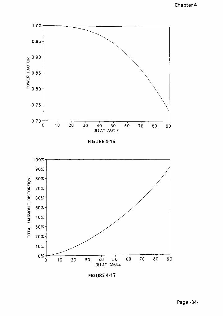
Chapter 4
1.00
10 20 30 40 50 60
DELAY ANGLE
70 80 90
FIGURE 4-16
100%
10 20 30 40 50 60
DELAY ANGLE
70 80 90
FIGURE 4-17
Page -84-

Chapter4
4.14 OUTPUT VOLTAGE CONTROL LOOP:
The PFC current modulator controller displayed in Figure 4-9 forces the power
converter to behave as a controlled current source. Both method of implementingthe current modulator function, Peak or Averaged Current control, will produce
output voltage that will vary as load and input line varies. The power converter
circuit can be modeled by a controlled current source driving the output port
impedance. Figure 4-18 displays a simple block diagram view of such model.
The output voltage of Figure 4-18 is a function of the current source magnitude and
output impedance:
vo= Vm,Z0) (4-67)
Where the variables are:
1 =IMm Msiniat) and Z0
=
<Zc+Rc)lRLoad
The only variable in equation (4-67) suitable for closed loop control is the magnitude
of the controlled current source, lM.
The current modulator controllers of Figures 4-10 and 4-1 1 produces the modulating
signal based on the current reference signal iRef. The current reference iRef\s a scaled
down signal derived from the input voltage vs as shown in Figure 4-9. The
magnitude the current control source of Figure 4-18 is determined by the magnitude
of iRef. To achieve output voltage control, the magnitude of iRefmust be the exact
value necessary to produce a corresponding magnitudeof the controlled current
source to balance the effects of output load and input voltage fluctuations. To
obtain dynamic voltage regulation, it is then necessary for the magnitude of iRefto
be a function of both input voltage and output voltage:
iRef= f vsit),v0 (4-68)
A conceptual block diagram of an additional voltage control loop to enable output
voltage regulation displayed in Figure 4-19. The current modulator function is
Page -85-

Chapter 4
supplemented by an outer voltage control loop. The function of the outer voltage
control loop is to modify the magnitude of ifle/-dynamically to compensate for input
voltage and output load variations.
ifiefsignals in Figures 4-9, 4-10 and 4-11 were a constant scaled version of the input
voltage vs. The voltage control loop of Figure 4-19 provides the dynamic control of
scaling of the reference signal based on a control voltage vcnt- The control voltage is
generated by comparing the output voltage to a desired voltage reference vRef. The
difference, verr, is amplified by an error amplifierwith frequency dependent gain Gv.
The current reference input of the current modulator controller is a product of the
scaled input voltage reference signal and the control voltage signal. The magnitude
of ifle/'is then controlled by modifying the magnitude of the control voltage vcnt-
Referring to Figure 4-19, the error voltage can be expressed as:
=vK -vt
(4-69)err o vo ref
Where Kv0 is the scaler for the output voltage sensing.
The control voltage expression is:
v =G vcnt v err
Combining with the input voltage sensing to derivethe current reference signal iRef.
iB =v K K v
Ref s vin m cnt
= vK . K G v
s vin m v err
v K K G iv K - v )s vin m v o vo ref
(4-71)
Let:
K =K Ka vin m
ifle/-expression:
Page -86-

Chapter 4
iRpf= vKG ivK -v j (4-72)
iief s a v o vo ref
Notice equation (4-72) is in the form of equation (4-68)
Page -87-

Chapter 4
=4= Co
Q
<
O
+
VS
FIGURE 4-18
RL IL(t)L
D
iL(t)
->
->
CURRENT
MODULATOR
CONTROLLER
d(t)
Q
\/ ,c(t)
iref
c
Re
+
=vc(t)
10
+
VO<
o
vs(t)
Kvin
vcnt
Gv < ++
Kvo ^
multiplier gain
Km
BOOST PFC WITH OUTER VOLTAGE CONTROL LOOP
Vref
FIGURE 4-19
Page -88-

Chapter 4
4.15 SMALL SIGNALANALYSIS:
A small signal model for the generic Boost Converter can be derived by introducing
small signal perturbations about the quiescent operating point in the state space
averaged equations([2]). The model can be further extended for current
programmed converters by incorporating the current information within the
expression for duty cycle([3], [4], [5]). The model is very useful for design of control
circuits for a Boost Converter but is of little value for the Boost Converter in power
factor correction application.
Equation (4-41) and (4-46) describes the duty cycle expression as a time varying
function with frequency equal to twice the line input frequency, 2a. In addition, the
control current source behavior of the pfc Boost Converter is highly non-linear when
expressed as output variables of voltage, current and load resistance. The function of
the current source in transmitting the input power to the converter's output must be
accomplished with the input port of the converter appearing resistive to the input
line to accomplish PFC
Equation (4-70) is rewritten as:
i_ Xt) = vit)K vt
(4-73)Ref s a cnt
The large signal condition for power factor correction dictates the inductor current
of the converter to behave as an amplified version of the reference current:
iAt) = Kip it) = K v it)K v,
(4-74)L i Ref i s a cnt
Ki is the gain from the current source reference iRefto the inductor current il-
Comparing equation (4-74) to equation (4-20) :
pEff K K v
i a cnt
Since the inductor current is the input current of the converter,the power input to
the PFC Boost Converter can be expressed as:
Page -89-

Chapter 4
P. it) = v it)iAt) = v it)K v it)K vin s L s i s a icnt
=V2
sire
2(cot)P"
if v
g i a cnt
(4-75)
Using Trig identity:
2 1 cos(2coi)sin iwt) =
P. (t)=in
1 cos(2co) K.K vi a cnt
Where Kb = Ki Ka.
P it) =vL
in rms
1 - cosi2at) Khvrb cnt
(4-76)
Equation (4-76) contains two power terms. A DC or average term and an AC or time
varying term:
P =Vs
Kuvaog rms o cnt
(4-77)
p (f)= cosi2wt)K,vt
ac rms b cnt
(4-78)
and...
p. it) = P +P it)in avg ac
(4-79)
The power output of the converter can be expressed as:
P0it) = zPAt)=
zPwg+ zPJt) (4-80)
Where e is the efficiency of the converterexpressed as the ratio of output power
delivered versus input power consumed by the converter.
Page -90-

Chapter 4
The output power also has a DC and an AC terms. If the output capacitor of the
converter is made sufficiently large, it would consume most of the AC power term
while leaving the DC power term to be delivered to the load. This is analogous to
having the AC voltage ripple on the output capacitor being much less then the DC
voltage on the capacitor. The AC term can then be ignored and using only the DC
term of the output power expression to derive the output voltage and current
variables. In practice, the bandwidth of the voltage control loop must be made to be
much less then the 2co frequency of the AC term to insure the AC term has an
insignificant affect on the duty cycle control voltage.The large signal condition
equations (4-41) and (4-46) must not be altered by the control circuit when the
output voltage ripple of 2q frequency is injected into the voltage control loop. The
small signal model of the pfc Boost Converter derived by using only the DC term is
valid by the necessity of narrow bandwidth voltage control loop. The higher
frequency poles and zeros of the generic Boost Converter do not contribute to any
significant factor at the low frequency portion of the voltage control loop. At higher
frequencies, the attenuation of the voltage control loop dominates and again
render the characteristic of the generic Boost Converter insignificant.
Using the approximation:
p~zP (4-81)O avg
To generate constant voltage output from equation (4-81), the power expression is
converter to a controlled current source:
=
p_o=^ =
lV% (4-82)lm~
y
~
yV"
V0 O 0
The expression for im is the small signal version of im depicted in Figure 4-18. The
term imcan be perturbed to deduce the small signal transfer function of the pfc
Boost Converter.
Three small signal expressions are necessary to fully describe the small signal
behavior of the PFC Boost Converter: the control to output transfer function; the
input to output transfer function; and the small signal impedance of the pfc Boost
Converter. The expression for im is perturbed about a quiescent control operating
Page -91-

Chapter 4
point to derive the small signal control to output transfer function. Referring to
Figure 4-19, it is desirable to select the control variable that is not time varying. In
addition, in practical design situations the compensation is typically applied at Gv to
produce the desirable control response. The term vcnt is the logical choice as the
control variable. It is the amplified and compensated version of the error voltage
between the output voltage and a voltage reference.
Perturbation is added to im and vcnt about the quiescent operating point:
V2
K.tlV +
7~
rms b \ cnt cnt
I + i =
mm y0
Where the overbar terms represent the small signal perturbation variables.
Using only the AC terms:
o
i V K.z ,. 0->\
m rms b (4-83)~~
vocnt u
Similarly, the input to output AC transfer function can be derived by perturbing im
and vrrns-
T 2 V K.tVm rms b cnt (4-84)
V"
u 0rms
"
The output power, considering only the DC term, can also be expressed by the
output variables:
p Vl (4-85)0 R
o
Equating equations (4-85) and (4-81):
Page -92-

0 2=
V2
K*vf> rms b cnt
Chapter 4
O b cnt
0.5
(4-86)
Substituting equation (4-86) into equation (4-84):
2K,&vtb cnt
PP\euO 6 cnt
0.5
After simplification:
= 2
KhZVrb cnt
R
0.5
(4-87)
The small signal output impedance of the pfc Boost Converter can be derived by
equating the small signal version of equation (4-85) to equation (4-81):
vz
rms b cnt
ro
Rearrange:
vi
V KKUr
rms b cnt
Substituting equation (4-86) into (4-88):
(4-88)
0 b cnt_
_
ro=
TTv'
~R<
b cnt
(4-89)
Page -93-

Chapter 4
Equation (4-89) concludes the small signal impedance of the PFC Boost Converter is
equal to the DC resistance of the load.
Equations (4-83), (4-87) and (4-89) constitute the small signal AC model of the PFC
Boost Converter. The equivalent circuit is displayed in Figure 4-20.
The equivalent circuit of Figure 4-20 is very different compared to the small signal
equivalent circuit of a generic Boost Converter. In actuality the right-half-plane zero,
the output capacitor esr zero, the complex pole pair of the output filter and the duty
cycle dependent gain of the generic Boost Converter are all still present in the PFC
Boost Converter. However since it is necessary for the PFC Boost Converter to
maintain very narrow voltage control bandwidth, i.e. much less then 2co to obtain
power factor correction, the effects of the generic frequency characteristics are of
minimal consequence and can be omitted.
FIGURE 4-20
The current source im is converted to output voltage by the parallel networkof c0,
r0ar\6Ro'.
Page -94-
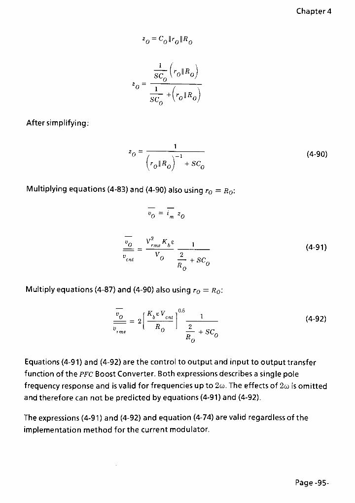
2o=
co II rolRo
Chapter 4
Zo=~
SC0\^Ro
s-c-0+VoWRo
After simplifying:
zo=
roWRo)
l
+ sco
(4-90)
Multiplying equations (4-83) and (4-90) also using r0= p0:
vn= I z
(J m O
V rms b 1
v Vn 2
Ro
(4-91)
Multiply equations (4-87) and (4-90) also using r0= r0:
= 2b cnt
R
0.5
+SCnR0
(4-92)
Equations (4-91) and (4-92) are the control to output and input to output transfer
function of the PFC Boost Converter. Both expressions describes a single pole
frequency response and is valid for frequencies up to 2co. The effects of 2co is omitted
and therefore can not be predicted by equations (4-91) and (4-92).
The expressions (4-91) and (4-92) and equation (4-74) are valid regardless of the
implementation method for the current modulator.
Page -95-

Chapter 4
4.16 INPUT VOLTAGE FEEDFORWARD:
Examination of equation (4-91) reveal the gain of the control to output transfer
function will vary as the square of the input voltage rms magnitude. In typical
applications the input line voltage will vary 50% from low line to high line
conditions (90-1 35VAC or 1 80 to 270VAC). The gain of the control to output transfer
function will vary by a factor of 2.25. If an universal input range is desired, the gain
of the control to output transfer function will vary by a factor of 9 for line variation
from 90VAC to 270VAC.
The gain dependence to input voltage magnitude can be eliminated by canceling
the voltage dependent term from the control to output transfer functional 1]). The
squared rms magnitude of the input voltage is feed into the control loop via a
divider function to eliminate the gain dependence. Figure 4-21 and Figure 4-22
displays two points of injecting the divider function into the voltage control loop. In
Figure 4-21 the divider is placed after the multiplierwhile in Figure 4-22 the divider is
placed after the Gv gain function.
The control to output transfer function with input voltage feedforward is:
X =
l(4-93)
cnt Vo 1. + SrR
Page -96-

Chapter 4
+
ys(t)
rms
vs(t)
RL iL(t)k D
e-v^ nrrmt N
iL(t)
">
->
CURRENT
MODULATOR
CONTROLLER
d(t)
\/IC
Re
10
Q
iref
+
:vc(t)
+
VO<
O
Y
Kvin
Divider
"7fT
->Square
vcnt
Gv < ++
multiplier gain
Km
Kvo <-
Vref
OUTER VOLTAGE CONTROL LOOP WITH INPUT VOLTAGE FEEDFORWARD
FIGURE 4-21
Page -97-
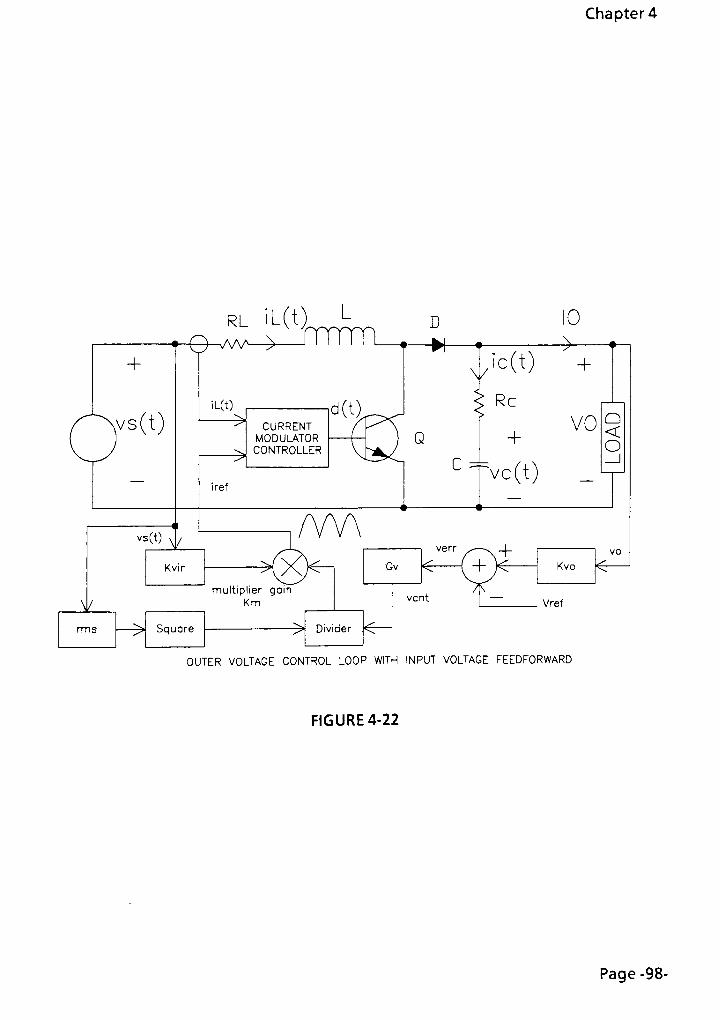
Chapter 4
+
v
^L
s(t)
vs(t)
RL lL(t)L
Ovvv^-mTTTTl
iL(t)
->
">
CURRENT
MODULATOR
CONTROLLER
d(t)
D
\/
10
c t +
Q
iref
C =k
Re
+
vc(t)
vo<
o
.
Kvin
multiplier gain
Km
->Square >
verr
Gv < ++
Divider ^
vcnt
Kvo <-
Vref
OUTER VOLTAGE CONTROL LOOP WITH INPUT VOLTAGE FEEDFORWARD
FIGURE 4-22
Page -98-

Chapter 4
4.17 CONTROL VOLTAGE SAMPLE AND HOLD:
The AC power term in equation (4-80) is ignored in the derivation of small signal
transfer function for pfc Boost Converter. However this assumption is no longer
valid when significant AC ripple exist at the output of the pfc Boost Converter. The
voltage control loop bandwidth must then be severely limited to provide sufficient
attenuation of the 2co AC term within the control loop to minimize the distortion of
the input currentwaveform. The distortion of the input currentwaveform is caused
by the control loop attempting to correct for the ripple voltage injected into the
loop. Considering the single pole frequency response of the control loop described
by equation (4-91), a 20db or better attenuation would require the bandwidth of
the control loop to be less then 2co + 1 0.
To eliminate the effect of the 2co AC term from distorting the current waveform, a
sample and hold circuit can be use to only sample the control voltage at the zero
crossing of the line input. Figure 4-23 shows the synchronization of the control
voltage sensing with the zero crossing of the line input. The voltage sample is held
until the next line cycle where a new value will be sampled. The ripple voltage on the
output is totally eliminated from affecting the voltage control loop. Figure 4-24
shows the additions of the sample and hold function in the voltage control loop. The
sample and hold is a zero order hold with transfer function of:
G AS) =^ (4-94)
s
Where t is the period of the sampler and S is the LaPlace operator.
Including the sample and hold in the control to output transfer function:
^0_ V 1l-e~ST
7"'
VQ 2 S (4-95)cnt
w + t>CnP
The introduction of the sample and hold to eliminate the current distortion effect of
the 2co voltage ripple effectively transformed thevoltage control loop into a sample
data system. Converting equation (4-95) intoZ-Transform equation:
Page -99-

Chapter 4
G iZ) =cnt
\Z \Z Transform of
V i
Vn ( 20s\ + scn\R
(4-96)
Where:
ST
Expanding the bracket term of equation (4-96) with partial fraction expansion:
V i
V*0
2Vo
s
Kb*R0
2Vo
VS{to+SCo)2
li +
C0R0
(4-97)
Using the transform of:
l l= and
S Z-\ S+X z_e-XT
Equation (4-97) becomes:
1 -z-i
Z-l
Z-e
-2T
C0R0
Kb*R0
2V
Simplified:
Gcnt^=
2V,
KbzR0 i_e
-IT
coRo
Z-e
-2T
coRo
(4-98)
Equation (4-98) is the Z-Transform transfer function from control to output of the
pfc Boost Converterwith input voltagefeedforward and output sense sample and
hold.
Page -100-

Chapter 4
The transforming of the voltage control loop into a sample data system by the use of
sample and hold also limits the bandwidth of the control loop. The sampling
frequency 2co of the sample and hold effectively limits the usable bandwidth of the
control loop to less then co. However, in practical application the bandwidth is
typically limited to less then 1 /5 th of 2co to prevent aliasing of the signalswithin the
control loop. For line frequencies of 50 or 60HZ, the voltage control loop is limited to
below20to24HZ.
Page -101-

Chapter 4
AC LINE
INPUT
OUTPUT
CAPACITOR
VOLTAGE
SAMPLES ni
Zero
Crossing
"7TT
+
rSvs(t)
vs(t)
FIGURE 4-23
RL iL(t)L
Qsw>- nrrm
iL(t)
->
">
CURRENT
MODULATOR
CONTROLLER
d(t)
D
Q
\/
iref fW\C
ic(t)
Re
+
vc(t)
Kvin
Divider
7TT
JL
->Square
JlL
S & H
vcnt
Gv < +
10
vo<
o
multiplier gain
Km
^L
Kvo
Vref
OUTPUT VOLTAGE CONTROL WITH INPUT VOLTAGE FEEDFORWARD AND CONTROL VOLTAGE SAMPLE AND HOLD
FIGURE 4-24
Page -102-

Chapter 4
4.18 PFC BOOST CONVERTER DRIVING CASCADED CONVERTERS:
The analysis so far has been with the pfc Boost Converter driving linear loads. The
resistance R0 is used to represent the DC ratio of the output voltage and current:
o
However in most applications the pfc Boost Converter serve as the front end to
additional voltage regulators that provides further conversion of the relatively high
DC output of the pfc Boost Converter into lower voltages. These cascaded DC to DC
converters also provides the line isolation and the fast transient response required by
the complex loads. The input characteristic of non-dissipative DC to DC converters
are inherently non-linear. The DC resistance P0 is not adequate to model the non
linear loading effects of the DC to DC converters. The loading effects of dissipative
DC to DC converters are adequately modeled by P0. Examples of non-dissipative DC
to DC converters are PWM Converters, FM Converters, Series and Parallel Resonant
Converters and Quasi-Resonant Converters.
The loads of the non-dissipative DC to DC converters are typically linear and can be
modeled by using a resistor. For any change at the of the pfc Boost Converter, the
cascaded regulators do not behave as a linear resistor. The current extracted by the
cascaded converters do not follow the voltage proportionally.
Let V0c and i0c represent the output DC voltage and current of the cascaded
converters. Let kc = DC gain of the Cascaded converters:
yoc
Where v0 is the DC output of the PFC Boost Converter.
Let Roc represent the DC load of the cascaded converter:
vy_oc_Roc~
ioc
Page -103-

Chapter 4
Let Poc represent the DC power delivered to the cascaded converter load:
p = v Ioc oc oc
Let PIC represent the power consumed by the cascaded converter:
P - *!ic
r
Where ec is the efficiency of the cascaded converter.
Pic can also be expressed as the power output of the PFC Boost Converter:
P = v Iic oo
And:
V I e = V I - k V I00 C OC OC C 0 oc
Solving for/0:
kcIoc
EC
The DC small signal input impedance of the cascaded converter, r;, can be derived by
solving the input equation of the cascaded converter for an incremental change in
the output of the PFC Boost Converter:
d.I jL^ Pr-2
dlo
'
dIo 'o
^ "
/C
Substituting forP/c:
-V
i oc
r = - VI~
-
KC 0
Page -104-

Chapter 4
Substituting fori0:
V e e
r.= --2-
= -- R (4-99)
A2
/A2 0C
^0*00 nc
Equation (4-99) state the DC small signal input impedance of the cascaded converters
is seen as a negative resistance. The value of the negative resistance equal to the DC
output load resistance of the cascaded converter, reflected into the input by the DC
gain kc and efficiency of the conversion. The cascaded converter function as constant
power sink where the current extracted by the cascaded converter is inversely
proportional to the output voltage of the pfc Boost Converter. The power extracted
by the cascaded converter is constant and equal to the power consumed by the loads
of the cascaded converter, plus losses represented by ec- The DC behavior of the
cascaded converter can then be modeled by a DC to DC transformerwith turns ratio
equal to kc. The load P0 in Figure 4-20 is replaced by a DC to DC transformer driving
load R0c- The revised Figure 4-20 is displayed as Figure 4-25.
The derivation for the small signal output impedance of the pfc Boost Converter is
based on input and output power expressions. Equation (4-95) is valid because P0
represent the ratio of output voltage and current produced by the controlled power
output of the converter. The parallel combination of R0 and r; is:
(v)
R0uv.v-v
~lv'
'o"
'o- '
vo Vo
[o lo
The negative incremental input resistance of the cascaded converter cancels the AC
small signal output resistance of the PFC Boost Converter. The output capacitor of
the PFC Boost Converter provides the single pole frequency response from DC.
The small signal transfer function described by equations (4-92), (4-93) and (4-96) are
revised without the AC output resistance r0:
Page -105-

Chapter 4
K^v0.5
b cnt
R SCr
(4-
100)
V 1
vt
V SCcnt u u
(4-
101)
G (Z) =cnt 2V
Kb*R0 1-e
-IT
0
Z - e
-2T
C0
(4-
102)
The term R0 in the DC gain of equations (4-101) and (4-102) represent the quiescent
operating point of the pfc Boost Converter.
Page -106-

Chapter 4
EFFICIENCY = c
>ro
Co Roc
DC MODEL OF CASCADED CONVERTER
SMALL SIGNAL EQUIVALENT CIRCUIT
WITH CASCADED CONVERTER LOAD
FIGURE 4-25
Page -107-

Chapter 4
4.19 FUNCTIONAL BLOCKDIAGRAM OF PFC BOOST CONVERTER:
An overall functional block diagram of the outer voltage control loop for pfc Boost
Converter is displayed in Figure 4-26. The output voltage is feedback through a
divider gain kvo. The feedback value is compared to a reference voltage vRef. The
error voltage is amplified by the transfer function GV(S). GV(S) is the frequency
dependent gain of the error amplifier. The output of the error amplifier is sampled
and hold to eliminate the injection of the AC ripple into the control loop. The sample
and hold output is multiplied with current reference derived through the divider
gain kuin. A multiplierwith gain of km is used to multiply the error amplifier output
with the current reference, the magnitude of the input rms voltage is squared and
divided out of the output of the multiplier. The output of the divider is feed into the
current modulator block to serve as the dynamic reference for the inductor current.
The current modulator control the current of the inductor to be an amplified replica
of the reference current.
The basic analytical steps are the same for either Peak Current or Average Current
Controlled Modulator. The assumption is the current modulator is capable of
replicating the current reference signal. The large signal distortion effects such as
delay angle and dwell angle are not relevant for small signal analysis. The outer
voltage control loop is rendered incapable of affecting the distortions generated
within the current modulator function.
The sample and hold is necessary to eliminate the effects of the AC ripple from
distorting the current modulator reference input signal. The AC ripple effect can be
reduced without the sample and hold by increasing the output capacitor value of
the PFC Boost Converter.The larger output capacitor will also decrease the
bandwidth of the converter described by equations (4-93), (4-1 01) and (4-102). The
effect of AC ripple can also be reduced by reducing the gain of GrfS) or making GV(S)
bandwidth limited to well below 2co. The effect on the overall bandwidth of the
control loop is the same. The 2co AC ripple must be attenuated to minimize the
distortion on the current reference signal. Gu(S) is typically designed to compensate
for the frequency response of the overall controlloop. Since the overall control loop
is inherently stable because only a single poleaffects the roll off, GV(S) can be made
into a constant gain term use to set the overall gain-bandwidth of the control loop.
Considering the bandwidth is constrained for the current waveform shaping large
Page -108-

Chapter 4
signal function of the converter, a more complex GV(S) characteristic yields only
modest improvement in the small signal response. A PFC Boost Converter is
governed by the large signal current waveform shaping behavior of the current
modulator.
Page -109-

Chapter 4
vref
RMS VALUE
Grms(S)
Kvin
SQUARE
MULTIPLIER GAIN
SAMPLE AND HOLD
-~\
Gsh(S)
CURRENT
MODULATOR
TRANSFER FUNCTION
(X>> Km -K3)-* Gim<S)
Kvo
CLOSED-LOOP BLOCK DIAGRAM FOR PFC BOOST CONVERTER
FIGURE 4-26
Page -110-

Chapters
CHAPTER 5
SIMULATIONAND VERIFICATION
5.1 BASIC BOOST CONVERTER SIMULATION TEMPLATE:
The operation of the pfc Boost Converter can be simulated with PSPICE using the
state space averaged large signal model as described by equations (4-1 5), (4-24) and
(4-25). The basic converter model was originally introduced by Bello with Berkeley
SPICE2 based on the results presented by Dr. Middlebrook. For this Thesis the Bello's
models were revised for PSPICE and used as the basic subcircuit module for the
simulation ofpfc Boost Converter.
The basic Boost Converter PSPICE equivalent circuit model is displayed in Figure 5-1 .
The PSPICE file for Figure 5-1 is listed in Table 5-1 . The DC to DC transformer
subcircuit dc-boost simulates the DC behavior of the Boost Converter. The step up
gain of the DC to DC transformer dc-boost is a function of the duty cycle signal at
node e.
Referring to Figure 5-1 and Table 5-1 , the input current of the subcircuit is measured
by the zero volt dc source vmtr. The effect of duty cycle is sensed at node e as a 0 to1
volt signal representing 0% to 100% duty cycle. The voltage across the primary
nodes, f and b, is equal to the voltage across the secondary nodes, d and c, multiplied
by 1 minus the signal at node e. This in effect modeled the (1-z>) gain of the Boost
Converter at DC. The secondary nodes are driven by a current source with its
magnitude equal to the input current measured by vmtr multiplied by 1 minus the
signal at node e. The input to output transfer function of the DC to DC transformer
match the behavior described by equation (4-27). The non-ideal terms are added as
external circuit components when the subcircuit is inserted into the whole pfc circuit
model. The feature of the subcircuit model is the inductor current is reflected into
the secondary side of the DC to DC transformerwhich properly models the effective
multiplication of the actual inductance by the duty cycle signal.
Page-111-

Chapter 5
dc_boost
FIGURE 5-1
SUBCIRCUIT DEFINITION
.subckt dc_boost a b c d e
gin a b value = { (I(vntr)*v(c,d))/v(a,b)eo f d value = { v(a,b)/(l-v(e)j }vmtr f c dc 0
rd e 0 1G
.ends
*
TABLE 5-1
Page-112-

Chapters
5.2 SIMULATION OF PFC BOOST CONVERTERWITH AVERAGE CURRENT
CONTROL :
The PSPICE model for Boost Converterwith average current control is displayed in
Figure 5-2. The accompany PSPICE file is listed in Table 5-2. The inductor L and the
series resistor RL is connected on the primary side of the DC to DC transformer dc-
boost. The model effectively implemented the behavior of the Boost Converter
described by equation (4-26).
The line voltage modeled by Vin is fullwave rectified by using an absolute value
function voltage-controlled-voltage-source model Ein. The current reference input
to the error amplifier, modeled by an ideal opamp, is Eref which is a scaled replica of
the fullwave rectified input voltage. The inductor current is sensed by the zero
voltage DC voltage source Vsen. The current through Vsen is the control input to the
current-controlled-voltage-source model Hse. The state space averaged equation
based DC to DC transformer model has effectively averaged the state variables over
the switching cycle. The switching frequency component is removed from the model
displayed in Figure 5-2. The error amplifier is compensated by Rz and Cz. The
dependent voltage source model Ecmp divides the opamp output by the peak value
of the saw tooth signal to derive the continuous duty cycle signal described in
equation (4-43). Finally Edut limits the duty cycle signal to be within the range of OV
(0%)to1V(100%).
Page -113-
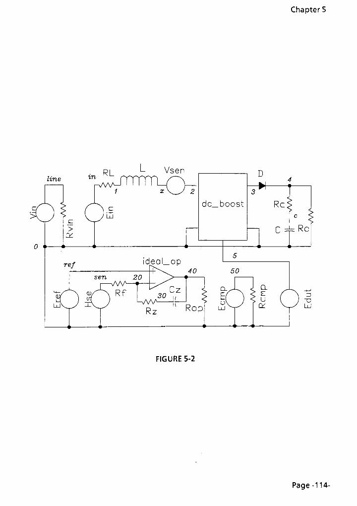
Chapters
L Vsen
FIGURE 5-2
Page -114-

Chapters
TABLE 5-2
PSPICE file for PFC Boost Converterwith average current control.
THOMAS YEHBST_PFC1.CIR
* FILE DESCRIPTION
* State Space model template file for a boost converter operating in*continuous conduction mode used in power factor correction with
*average current control.
* DEFINE NOMINAL PARAMTERS
.param L = 1.0m
.param RL = 0.01
.param Rload = 200
* CIRCUIT DESCRIPTION
* Input line source: 60HZ sine 230Vrms
Vin line 0 sin(0 325 60 0 0 0)
Rvin lineO 1Meg
* Full wave rectified line:
Ein in 0 value = {abs( V(line) )}
RL in 1 {RL}
L 1x{L}
Vsen x 2 dc 0
*The boost dc-dc transformer subcircuit call:
X1 2 0 3 0 5 dc_boost
*Output elements:
d1 3 4dmod
Re 4c1e-3
Co c0 820u
Ro 4 0 {rload}
* Current sense and control:
Eref ref 0 value = { 0.01*v(in) }
Hse sen 0 Vsen 0.35
Rf sen 20 1 OK
Rz 20 3015K
Cz 30 40.001 u
X2 ref 20 40 0 ideal_op
Rop 40 01G
Ecmp 50 0 value = { (v(40)+0.1)/3.5 }
Rcmp 50 0 1 G
Edut 5 0 table {v(50)}= (0,0) (1,1)
*SUBCIRCUIT DEFINITION
.subekt dc_boost a b c d e
vmtr a f dc 0
ein f b value = { v(c,d)*(1-v(e)) }
go d c value = { l(vmtr)*(1-v(e)) }
ro dc1G
rd e01G
.ends
.subekt ideal_op ninv inv out gnd
rin ninv inv 1G
eo out gnd table {v(ninv.inv)} =
+ (0,0) (2u, 0.1) (20u, 1) (70u, 3.5)
.ends
* DEVICE MODELS
.model dmod d(rs=1)
* SIMULATION DIRECTIVES
.stepparam L list 1m 5m 10m
.tran 0.5m 50m 0 0.5m
.options limpts=10000 itl5=0 abstol=1n VNTOL=1
.probe
.end
Page -115-

Chapter 5
The output of the current reference source, Eref, is equal to the absolute value
voltage source, Ein, multiplied by 0.01 . The current sense voltage source, Hse, has the
transfer gain of 0.35. The effective resistance, REffl of the PFC Boost Converter can be
calculated:
, , ,0.01(325)
Peak Programmed inductor current =1, ,
= = 9.2857 Amperes.LPeak 0_35
Vin Peak 325
P,, = = 35 Ohms.Eff /._
,9.2857
LPeak
The simulation runs of the PSPICE model listed in Table 5-2 is carried out for inductor
values of \mH, 5mtfand 10mff. The corresponding Q values are calculated:
REff~RL 35-0.01
ForL = l mH, Q =- = = 92.814
coL 2n60(lmH)
REff~RL 35-0.01
ForL = 5 mH, Q =r
=-
nn/c rn
= 18.563
coL 2n60(5mtf)
REff~RL 35-0.01
For L = 10 mH,Q = =~ = 9.2814
'^
aL 2n60(10/nfl)
The delay angles and delay durations for the three Q values are calculated:
For Q = 92.814, Y= tan~\-) = tari"1(92814) =
0617
2y = 12346= 57 .157p second duration.
ForQ = 18.563, Y= tan
~
lt - ) = tan ~\gg3
) =3.0836
2y =6.1672
= 285 52\i second duration.
For Q = 9.2814, Y= tan'H-)^ tan~l(f2~^) =
61495
2y =12.299= 569. 39u second duration.
Page -116-

Chapter 5
The calculated results corresponded to the simulated results displayed in Figures 5-3
to 5-20.
Figures 5-3 to 5-8 are the simulation results with inductor value of ImH. Figures 5-9
to 5-14 are the simulation results with inductor value of 5mH. Figures 5-1 5 to 5-20 are
the simulation results with inductor value of 10mH. Figure 5-21 superimposes an
expanded view of the inductor current for the three inductor values. Figure 5-22
superimposes an expanded view of the duty cycle control voltage for the three
inductor values.
The simulation results verified the waveform shaping performance of the pfc Boost
Converter with average current controlled current modulator The effectiveness of
the current shaping is displayed in Figures 5-3, 5-9 and 5-15. The inductor current
follows the fullwave rectified voltage waveform except during the delay interval.
The delay angle becomes more drastic as the inductor value is increased from 1 mH to
10 mHwhich is in accordance with the results predicted by equations (4-34) and (4-
41). The inductor currentwaveform in Figure 5-4 shows very little delay angle. The
delay angle in the simulation result of Figure 5-10 is equal to5.8428
or 270. 5u
seconds. This correspond with the calculated value of6.1672
based equation (4-34).
The simulated delay angle displayed in Figure 5-16 is equals to11.511
or 532 9u
seconds. This also corresponded with the calculated value of 1 2.299. The simulated
duty cycle control signal waveforms displayed in Figures 5-5, 5-11 and 5-17 follows
the predicted waveform displayed in Figure 4-8.
The delay angles for the three inductor values are superimposed in one simulation
output displayed in Figure 5-21. The slight oscillatory response in the current
waveform is attributed to the compensation of the average current control error
amplifier by Rf, Rz and Cz.
Page 117-

Chapter 5
FIGURE 5-3
Simulation result with inductor value = 1 mH.
Top Plot: Input Voltage and OutputVoltage.
Bottom Plot: Inductor Current.

Chapter 5
FIGURE 5-4
Simulation result with inductor value = 1 mH.
Expanded View of the Inductor Current.
- T
+
i
+
<x
o Page -119-
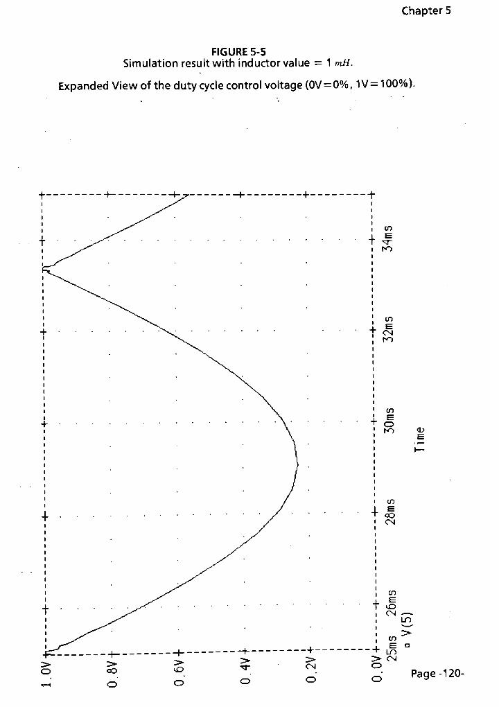
Chapter 5
FIGURE 5-5
Simulation resultwith inductor value = 1 mH.
Expanded View of the duty cycle control voltage (0V= 0%, 1V= 100%).
CL>
Page -120-

Chapter 5
FIGURE 5-6
Simulation resultwith inductor value = 1 mH.
Output voltage starting from 0 volt.
t r + 1 CO
s
OLO
CO
O"3-
cn
CDro
<L>
+ -r CD
CM
Page -121-

FIGURE 5-7
Simulation resultwith inductor value = 1 mH.
Inductor current.
Chapter 5
CD
Page -122-

FIGURE 5-8Simulation resultwith inductor value = 1 mH.
Duty cycle control voltage (0V= 0%, 1V=100%).
Chapter 5
<D
Page -123-

FIGURE 5-9
Simulation resultwith inductor value = 5 mH.
Top Plot: Input Voltage and OutputVoltage.
Bottom Plot: Inductor Current.
Chapter 5
<D
Page -124-

FIGURE 5-10
Simulation resultwith inductor value = 5 mH.
Expanded View of the Inductor Current.
Chapter 5
<u
Page -125-

Chapter 5
FIGURE 5-11
Simulation result with inductor value = 5 mH.
Expanded View of the duty cycle control voltage (0V=0%, 1V= 100%).
Delay Interval measured = 270.5u seconds.
ooo
CD CD CD
CD CD CD
en
ro
r 1 *-< O
-.
ro to co
CO
CM
ron n n
^-t CM
UU "O
<D
Page -126-

Chapters
FIGURE 5-12
Simulation resultwith inductor value = 5 mH.
Output voltage starting from 0 volt.
t"T +1-
OT
+
o
LO
CO
O
co
CD
ro
+ +
CO
o
CM
<D
O
OLO
OCD
O
OrO
CD
CDCM
O
CD Page -127-
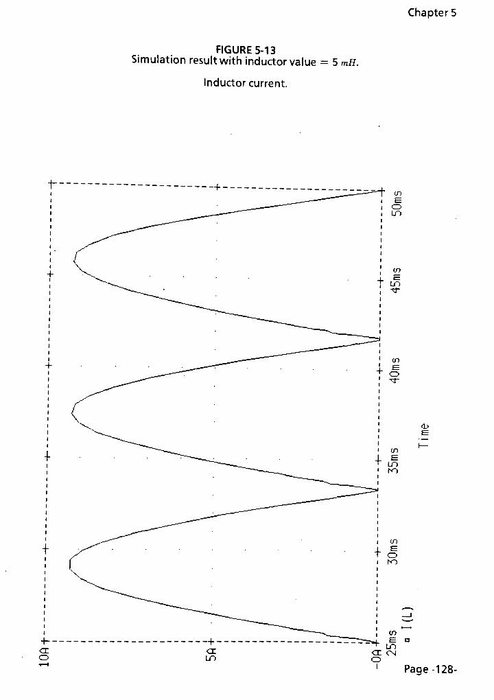
Chapter 5
FIGURE 5-13Simulation resultwith inductor value
Inductor current.
5 mH.
<D
Page -128-

Chapters
FIGURE 5-14
Simulation resultwith inductor value = 5 mH.
Duty cycle control voltage (0V= 0%, 1V= 100%).
Page -129-

Chapters
FIGURE 5-15
Simulation resultwith inductor value = 10 mH.
Top Plot: InputVoltage and OutputVoltage.Bottom Plot: Inductor Current.
<D
E a
Page -130-

FIGURE 5-16
Simulation result with inductor value = 10 mH.
Expanded View of the inductor current.
Chapters
Page -131-

Chapter 5
FIGURE 5-17
Simulation resultwith inductor value = 10 mH.
Expanded View of the duty cycle control voltage (0V= 0%,1V= 100%).
Delay Interval measured = 532.9u seconds.
oO
o o O
CM
O
CD CD CD
CD CD CD
OO o
COT-t T-l O
s
ro
ro ro co
UJUJUJ
KJOC7)
o~>tj-
CM
CO to ro to
ro ro lo
CM
ron u n
*4
^hCN-
UUT3
CO
CDro
co
CO
CM
CO
CO
CM
CD
LO
cnr,
s i a :-f-
i r\ < >
O
O
LO'
CM
Page -132-
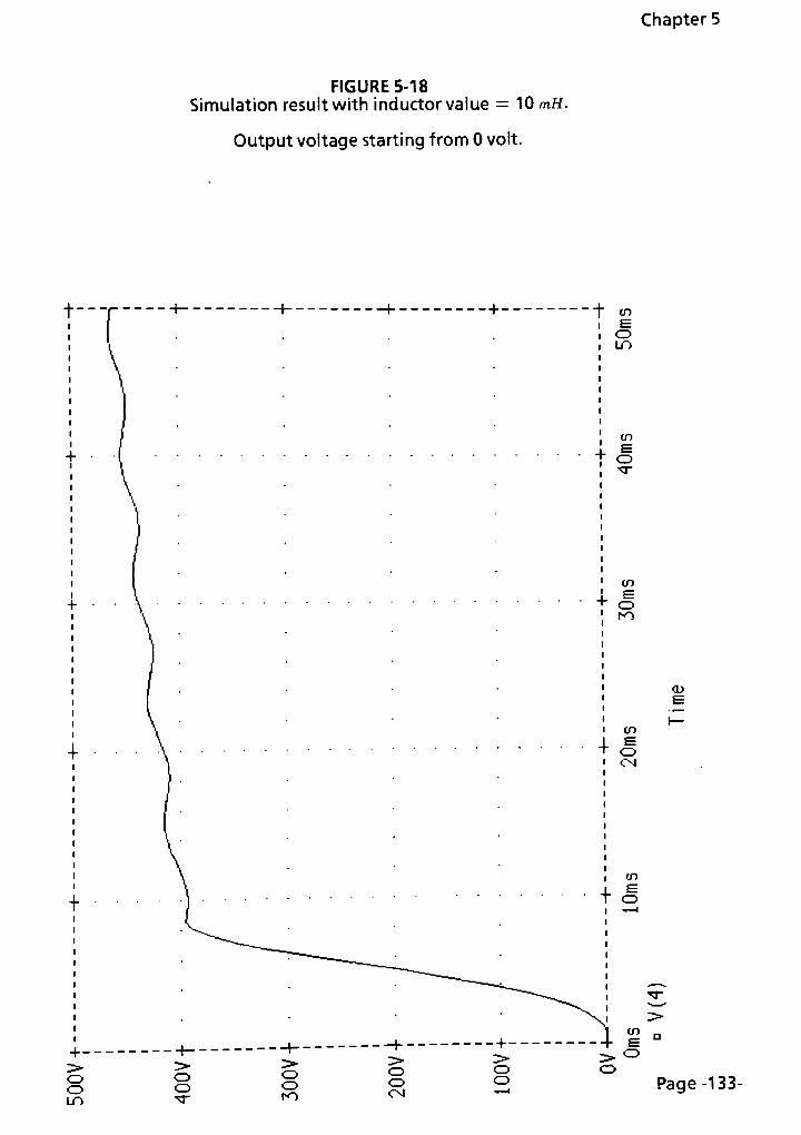
Chapters
FIGURE 5-18
Simulation resultwith inductor value = 10 mH.
Output voltage starting from 0 volt.
t-|
<D
Page -133-

FIGURE 5-19Simulation resultwith inductorvalue = 10 mH.
Inductor current.
Chapter 5
CD
+ 1 - --I----+-- +- -- --^f-
LO
<x
o
cr
cO
cr cr cr
CMcr
o
CM
Page -134-

Chapter 5
FIGURE 5-20Simulation result with inductor value = 10 mH.
Duty cycle control voltage (0V=0%,1V= 100%).
CD CD CD
CD CD CDCD CD CD
Page -135-

FIGURE 5-21Simulation resultwith inductor value = 1 mH, 5 mH, 10 mH.
Expanded View of the inductor currents.
Chapter 5
<D
cr lo
CD CM
1 Page -136-

Chapter 5
FIGURE 5-22Simulation resultwith inductor value = 1 mH, 5 mH, 10 mH.
Expanded View of the duty cycle control voltages (0V=0%, 1V=100%).
CD
Page -137-

Chapters
5.3 SIMULATION OF PFC BOOST CONVERTERWTTH PEAK CURRENT
CONTROL :
The Boost Converter with peak current control PSPICE model is displayed in Figure 5-
23. The accompany PSPICE file is listed in Table 5-3. The current control section of
Figure 5-2 is replaced by the model which effectively implemented the behaviorof
the Boost Converter described by equation (4-44).
The voltage source Em1 calculates the slope of the positive goinginductor current
ramp by implementing equation (4-46). The voltage across the inductor is calculated
by subtracting the voltage drop of RLfrom the input voltage. The slope, ml, is equal
to the voltage across the inductor divided by the inductor value.
The negative going slope of the inductor current, m2,is calculated by the voltage
source Em2. Equation (4-46) is carried out by subtracting the voltage across RL and
Vo from the input voltage. The negative slope, m2, is then calculated by dividing the
voltage across the inductor by the inductor value. Em2 can be used toprovide for
optimum slope compensation for the current control loop. The duty cyclecontrol
signal is calculated by implementing equation (4-44). The compensation slope value.
mc, is left as a parametricvariable and will be substituted at run time. The voltage
source Ed limits the duty cycle control signal from OV (0%) to 1V (100%). The current
reference is provided by scaling the absolute valueoutput of the voltage source Ein
by 0.01 . The inductor current is sensed by Hse which has transfer gain of0.5.
The simulation is carried out for inductor values of 1 mH, 5 mH and 10 mH. The
corresponding dwellangles and durations can be calculated from
equation (4-54):
For L = 1 mH, DUgx
= 0.67, cj> =18.770
= 868.98u seconds.
ForL = 5 mH, DMax= 0.85, $ =
9.431
= 436.62u seconds.
For L = 10 mH, D^
= 0.82, <J> =8.232
= 381.Up seconds.
These calculated resultscorresponded to the simulated results displayed in Figures 5-
24 to 5-41.
Page -138-

Chapter 5
line
0 * *
znRL
>
c
LxJ
L Vsen
dc_boost
D
Re:
C Ro
ref sen
LJ
cu
L
LYk5
72
/0 //
*5
?
"D
LJ
FIGURE 5-23
Page -139-

Chapter 5
TABLE 5-3
PSPICE file for PFC Boost Converterwith peak current control.
BST PFC4.CIR THOMAS YEH
* FILE DESCRIPTION
* State Space model template file for a boost converter operating in
*continuous conduction mode used in power factor correction with
*peak current control.
* DEFINE NOMINAL PARAMETERS
.param L = 1m
.param RL = 0.01
.paramRload = 200
.paramTs = 20u
.parammc = 25K
* CIRCUIT DESCRIPTION
* Input line source: 60HZ sine 230Vrms
Vin line 0 sin(0 325 60 0 0 0)
Rvin line 0 1Meg
* Full wave rectified line:
Ein in 0 value = {abs( V(line) )}
RL in 1 {RL}
L 1x{L}
Vsen x 2 dc 0
*The boost dc-dc transformer subcircuit call:
X1 203 012dc_boost
* Output elements:
d1 3 4 Dmod
Re 4c1e-6
Co c0 820u
Ro 4 0 {rload}
* Current mode control section:
Em1 10 0 value = { (v(in)-(l(Vsen)*RL))/L }
Rm1 10 01Meg
Em2 11 0 value = { abs((v(in)-(l(Vsen)*RL)-v(4))/L) }
Rm2 11 0 1MegEdu 13 0 value = { (v(ref)-V(sen))/(Ts*(0.5*v(10) +mc)) }
Rdu13 01MegEd 12 0 table = { v(13) } = (0, 0) (0.5, 0.5) (1, 1)
* Current sense and Voltage reference:
Eref ref 0 value = { 0.01*v(in) }
Rerf ref 0 1 Meg
Hse sen 0 Vsen 0.5
Rhs sen 0 1Meg
*SUBCIRCUIT DEFINITION
.subekt dc_boost a b c d e
vmtr a f dc 0
ein f b value = { v(c,d)*(1-v(e)) }
go d c value = { l(vmtr)*(1-v(e)) }
ro dc1G
rd e01G
.ends
.subekt ideal_op ninv inv out gnd
rin ninv inv 1 G
eo out gnd table {v(ninv, inv)} =
+ (0,0) (2u, 0.1) (20u, 1) (70u, 3.5)
.ends
*DEVICE MODELS
.modeldmod d(rs=1)
* SIMULATION DIRECTIVES
.stepparam L list 1m 5m 10m
.tran 0.1m 50m 0 0.25m
.options limpts=10000 itl5=0 abstol=1n vntol= 10u
.nodesetv(12)= 1.0
.probe
.end
Page -140-

Chapters
Figures 5-24 to 5-29 are the simulation results with L = 1 mH. Figures 5-30 to 5-35 are
the simulation results with L = 5 mH. Figures 5-36 to 5-41 are the simulation results
with L = 1 0 mH. Figure 5-42 is an expanded view of the inductor current for the
three simulation runs superimposed in one diagram for comparison. Similarly,
Figure 5-43 is an expanded view of the duty cycle control signal forthe three
simulation runs superimposed in one diagram for comparison.
The simulation results verified the waveform shaping performance of the pfc Boost
Converterwith peak current controlled current modulator. The effectiveness of the
current shaping is displayed in Figures 5-25, 5-31 and 5-37. The inductor current
follows the fullwave rectified voltage waveform except during the dwell interval.
The dwell angles decreases as the inductor value is increased from 1 mH to 10 mH
which is in accordance with the results predicted by equations (4-50) and (4-54). The
increasing inductor values has an opposite effect on the dwell angles compared to
the effect of increasing inductor values has on the delay angles. The inductor current
waveform in Figure 5-25 displays significant amount of dwell angle. The simulation
result of Figure 5-25 for the dwell angle is measured to be18.883
or 874.2u seconds.
This corresponded with the calculated value of18.770
based equation (4-54). The
simulated dwell angle displayed in Figure 5-31 is measured to be9.5
or 440u
seconds. This also corresponded with the calculated value of 9.431. The simulated
duty cycle control signal waveforms displayed in Figures 5-26, 5-32 and 5-38 follows
the predicted waveform presented in Figure 4-12.
The dwell angles for the three inductor values are superimposed in one simulation
output displayed in Figure 5-42.
Page -141

FIGURE 5-24
Simulation resultwith inductor value = 1 mH.
Top Plot: Input Voltage and OutputVoltage.Bottom Plot: Inductor Current.
Chapter 5
Page -142-

Chapter 5
FIGURE 5-25
Simulation result with inductor value = 1 mH.
Expanded View of the Inductor Current.
t +
T
co
e
ro
+
t
-f-
cr
o
CD
Page -143-

Chapter 5
FIGURE 5-26
Simulation result with inductor value = 1 mH.
Expanded View of the duty cycle control voltage (0V=0%,1V= 100%).
Delay Interval measured= 874.2u seconds.
to ^O CO
1 r- cO
uu (Or-
-> cO LO
cO
Oo~>
ro to <o
LU LU LUr^ o CM
to LO
<r
to CM r-
to ro oO
it n II
^H CM
LJ C_> o
CD
o CD
o CD
CO O
o
o
o
CD
CM
CD Page -144-
Chapter 5
FIGURE 5-27
Simulation resultwith inductor value = 1 mH.
Output voltage starting from 0 volt.
1 m
+
+
-r
T
oCD

FIGURE 5-28Simulation resultwith inductor value = 1 mH.
Inductor Current.
Chapter 5
<D
Page -146-
FIGURE 5-29Simulation resultwith inductor value = 1 mH.
Duty cycle control voltage (0V= 0%, 1V= 100%).
Chapter 5
t
+
+
T
+-
O
CD
Page -147-

FIGURE 5-30
Simulation resultwith inductor value = 5 mH.
Top Plot: Input Voltage and OutputVoltage.
Bottom Plot: Inductor Current.
Chapter 5
CD
Page -148-

Chapters
FIGURE 5-31
Simulation resultwith inductor value = 5 mH.
Expanded View of the Inductor Current.
CD
Page -149-

Chapters
FIGURE 5-32
Simulation result with inductor value = 5 mH.
Expanded View of the duty cycle control voltage (0V= 0%, 1V= 100%).
Delay Interval measured = 344.7u seconds.
CO CM zr
O r-vO
CD TT "vT
COCM co cO
1^T
ro
ro to ">
LU LU LU
LO CD r-
CM CD
^r
CO ro CM 'sT
to to to
CM
tou It it
T 1 CM -.
(_) <> TD
CD
Page -150-

FIGURE 5-33
Simulation resultwith inductor value = 5 mH.
Output voltage starting from 0 volt.
Chapter 5
t" +-
t CO
oLO
+
CO
O
XT
CO
sCD
to
CD
+4-
CO
CD
CM
TT
co
CD
OO
LO
OCD
OOro
CD
CD
CM
- + -
o
CD
^x
4 g -
Page -151-

Chapters
FIGURE 5-34
Simulation result with inductor value = 5 mH.
Inductor current.
CD
Page -152-
FIGURE 5-35Simulation resultwith inductor value = 5 mH.
Duty cycle control voltage (OV= 0%,1V= 1 00% ).
Chapter 5
<D
Page -153-

FIGURE 5-36
Simulation result with inductor value = 10 mH.
Top Plot: Input Voltage and OutputVoltage.
Bottom Plot: Inductor Current.
Chapter 5
Page -154-

FIGURE 5-37
Simulation result with inductor value = 10 mH.
Expanded View of the inductor current.
Chapters
<D
Page -155-

Chapters
FIGURE 5-38
Simulation result with inductor value = 10 mH.
Expanded View of the duty cycle control voltage (0V= 0% ,1 V= 1 00%).
Delay Interval measured = 389.3u seconds.
to ^r CO
1 oO CO
LU* 1 LO
ro CO r-
LO
CD
LO
,
to to ^o
LU LU LU
-or- ro
to CT)
CT)
to CM CO
to to to
II II u
1 CM
LJ LJ o
CD
Page -156-

Chapter 5
FIGURE 5-39
Simulation resultwith inductor value = 10 mH.
Output voltage starting from 0 volt.
t T +_j.
OT
o
LO
+ CD
co
so
to
+ +
CO
e
CD
CM
TT
co
O
CD
M CO
OCD
LO
CD
CD
OCD
ro
o
o
CM
oCD Page -157-

FIGURE 5-40
Simulation resultwith inductor value = 10 mH.
Inductor current.
Chapters
CD
Page -158-

FIGURE 5-41Simulation resultwith inductor value = 10 mH.
Duty cycle control voltage (0V=0%, 1V= 100%).
Chapters
CD
CD
o Page -159-

Chapter 5
FIGURE 5-42
Simulation resultwith inductor value = 1 mH, 5 mH, 10 mH.
Expanded View of the inductor currents.
CD
LO to CM
cr lo
CD CM
0Page -160-

Chapter 5
FIGURE 5-43
Simulation result with inductor value = 1 mH, 5 mH, 10 mH.
Expanded View of the duty cycle control voltages (0V=0%,1V= 100%).
Page -161

Chapter 5
5.4 SIMULATION OF PFC BOOST CONVERTERWITH OUTPUTVOLTAGE
CONTROL LOOP :
The PSPICE model for the PFC Boost Converterwith an output voltage control loopis displayed in Figure 5-44. The accompany PSPICE file is listed in Table 5-4. The
current modulator section is the average current controlled current modulator
model of Figure 5-2. The output voltage is sensed by the divider resistor Rdivl and
Rdiv2. The output of the dividers at node 6 is compared to a DC reference voltage,
Vref, at node 7. The difference error is amplified by subcircuit X3 which models an
ideal opamp. The reference for the current, modeled by Emul, is equal to the output
ofX3 at node 8 multiplied with the output of Eref. Eref is a scaled version of Ein. The
error amplifier gain is setup by the feedback resistor Rcmp. The simulation is carried
outwith the inductor value of 1 mH, resistive load of 200 Ohms and output
capacitance of 820 uF. These are the same values used to generate the simulation
results displayed in Figures 5-3 to 5-8.
The results of the simulation with Rvsetto 100K Ohms are displayed in Figures 5-45
to Figures 5-49. The regulation of the output voltage at about 400VDC by the
voltage control loop can be readily observed especiallywhen the output voltage is
compared to the simulation result displayed in Figure 5-6.
The distortion of the inductor current caused by the injection of 2co AC ripple into
the voltage control loop is illustrated in the bottom plot of Figure 5-46. The output
voltage ripple can be observed at the output of the voltage error amplifier. Figure 5-
49 shows the peak to peak value of the AC ripple present at the output of the
voltage error amplifier is about 1 .7V and it is superimposed on DC error signal of
2.2V. The resultant current reference signal to the current error amplifier is also
distorted as displayed in Figure 5-48.
Without a sample and hold function, the peak to peak amplitude of the AC ripple
injected into the loop is set by the loop gain at the frequency 2co. The distortion
produced by the AC ripple can be reduced by lowering the peak to peak amplitude
of the AC ripple at the output of the voltage error amplifier, X3. Figures 5-50 to 5-54
are the simulation results with the voltage error amplifier gain reduced by lowering
the value for Rv to 50K Ohms. The effect of the reduced loop gain is the control loop
now produces higher steady state output voltageas shown in Figure 5-50. However,
the distortion of the inductor current is also reduced as displayed in the bottom plot
Page -162-

Chapters
of Figure 5-51 . The corresponding peak to peak AC amplitude at the output of the
voltage error amplifier is about 0.5V and it is superimposed on DC error signal of
2.2V. The current modulator reference with the reduced voltage control loop gain
now has very small amount of distortion compared to Figure 5-48.
The effectiveness of the voltage regulation function is simulated by changing the
input voltage and output load of the PFC Boost Converter model. Figures 5-55 to 5-
59 displays the simulation resultswith 50% step down of the input voltage. Both the
simulated input voltage and output voltage are displayed in Figure 5-55. The step
change of the input voltage from 230Vrms to 125Vrms occurred at simulation time
of 50m second. Only a slight drop in the output voltage can be observed in the
simulation result. The corresponding increase in the inductor current is displayed in
the bottom plot of Figure 5-56. The simulation results confirmed the ability of the
PFC Boost Converter to function as a constant power regulatorwith voltage
regulation. Figures 5-57, 5-58 and 5-59 displays the response of the duty cycle signal,
current modulator reference signal and the output of the voltage error amplifier
due to the input voltage step change.
Figures 5-60 to 5-64 displays the response of the voltage regulation loop with an
output load step change. The input voltage is held constant while the output load
power is doubled at the simulation time of 50m second. A slight decrease in the
simulated DC output voltage can be observed in Figure 5-61 . The increase of the AC
ripple at the output voltage due to the additional load is also observed in Figure 5-
61. The additional output load must be compensated with corresponding increase in
the magnitude of the inductor current as seen in the bottom plot of Figure 5-61 . The
inductor current also exhibits greater amount of distortion, compared to Figure 5-
56, attributing to the additional AC ripple being injected into the voltage control
loop. Figure 5-64 displays the greater AC peak to peak amplitude at the output of
the error amplifier as compared to Figure 5-59.
Page -163-
Chapter 5
Ideal-P^Vref><
75
CL
FIGURE 5-44
Page -164-

Chapter 5
TABLE 5-4
PSPICE file for pfc Boost Converterwith outer voltage control loop.
PFCVFB.CIR THOMAS YEH
*FILE DESCRIPTION
*State Space model template file for a boost converter operating in
*continuous conduction mode used in power factor correction with
*average current control. An outer voltage control loop is included.
*DEFINE NOMINAL PARAMETERS
.param L = 1m
.param RL = 0.01
.param Rload = 200
.param Cv = 0.1 u
.param Rv = 1 0OK
.param Mulgain = 3.5
* CIRCUIT DESCRIPTION
* Input line source: 60HZ sine 230Vrms
Vin line 0 sin(0 325 60 0 0 0)
Rvin line 0 1 Meg
* Full wave rectified line:
Ein in 0 value = {abs( V(line) )}
RL in 1 {RL}
L 1x{L}
Vsen x 2 dc 0
Dby in 4 dmod
*The boost dc-dc transformer subcircuit call:
X1 2 0 3 0 5 dc_boost
* Output elements:
d1 3 4 dmod
Re 4 c 1 e-6
Co c 0 820u
Ro 4 0 {rload}
* Current sense and control:
Hse sen 0 Vsen 0.35
Rf sen20 10K
Rz 20 30 15K
Cz 30 40.001 u
X2 10 20 40 0ideal_op
Rop 40 01G
Ecmp 50 0 value = { (v(40)+0.1)/3.5 }
Rcmp 50 0 1 G
Edut 5 0 table {v(50)}= (0,0) (1,1)* Voltage feedback control loop:
Rdivl 4 6 770K
Rdiv2 6 0 10K
Vref 7 0 dc 5.0
Ccomp 6 8 {Cv}
*Rcomp 6 8 {Rv}
X3 7 6 8 0 ideal_op
Rx3 8 0 1 MEG
Eret ref 0 value = { 0.01 *v(in) }
Rerf ref 0 1 G
Emul 10 0 value = { v(ref)*v(8)/Mulgain }
Remul 10 0 1G
* SUBCIRCUIT DEFINITION
.subekt dc_boost a b c d e
vmtr a f dc 0
ein f b value = { v(c,d)*(1-v(e)) }
go d c value = { l(vmtr)*(1-v(e)) }
ro d c 1 G
rd e0 1G
.ends
.subekt ideal_op ninv inv out gnd
rin ninv inv 1 G
eo out gnd table {v(ninv,inv)} =
+ (0, 0) (2u, 0.1) (20u, 1) (70u, 3.5)
.ends
* DEVICE MODELS
.model dmod d(rs=,1)
.model switch vswitch(ron= 100 roff=1G von=2 voff=0.5)
* SIMULATION DIRECTIVES
'.step param Cv list 1 u 0.1 u 0.01 u
'.step param Rv list 200K 1 00K 50K
.four 120 i (I)
.tran 0.5m 50m 0 0.5m
.options limpts=10000 itl5=0 abstol=1n reltol=0.01
.probe
.end
Page -165-

Chapters
FIGURE 5-45
Simulation resultwith an output voltage control loop(Rv= 100KOhms)
Output voltage
t
T
+
+
O
oLO
^
CD
CD
^r-
o
CD
ro
oo
CM
CD
CD
t
+
+
CO
=
CD
CO
CDCM
CO
o
o
+
+
CO
s=
CD
cO
CO
s
CD
CO
CD^7"
CO
cm
CO
f S
CD
Page -166-

Chapter 5
FIGURE 5-46
Simulation result with an output voltage control loop(Rv= 100KOhms)
Top Plot: InputVoltage and Output Voltage.
Bottom Plot: Inductor Current.
CD
Page -167-
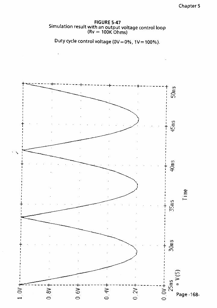
Chapters
FIGURE 5-47Simulation resultwith an output voltage control loop
(Rv= 100KOhms)
Duty cycle control voltage (0V=0%, 1V=100%).
CD
Page -168-

Chapter 5
FIGURE 5-48
Simulation resultwith an output voltage control loop(Rv= 100KOhms)
Current modulator reference.
f
+
+
+
T
+
>
Ol

Chapter 5
FIGURE 5-49
Simulation result with an output voltage control loop(Rv = 100KOhms)
Voltage error amplifier output.
t
4-
T
J
-r-
O
co
CD
LO
CO
s=
U~>
co
*=
CD
4-
CO
to
CO
to
<D
CO
O
rO
CD
Ol
en
+ LO
> C"M
OPage -170-

Chapter 5
FIGURE 5-50
Simulation result with an output voltage control loop(Rv= 50KOhms)
Output voltage
t
+
T
+
+
-r
o
o
LO
V
I
I
+ +
o
o
o
CD
to
O
CD
Ol
t
+
T
en
o
co
oOJ
co
CD
O
co
oO
+
CO
CD
CO
o"3-
4-
CO
CD
Ol
CD
-"3-
>
toH- S>
CD Page -171-

Chapter 5
FIGURE 5-51
Simulation resultwith an output voltage control loop(Rv = 50K Ohms)
Top Plot: InputVoltage and OutputVoltage.
Bottom Plot: Inductor Current.

Chapter 5
FIGURE 5-52
Simulation result with an output voltage control loop(Rv= 50KOhms)
Duty cycle control voltage (0V=0%, 1V=100%).

Chapter 5
FIGURE 5-53
Simulation result with an output voltage control loop(Rv= SOKOhms)
Current modulator reference.
1-
+
+
T
CM

Chapter 5
FIGURE 5-54
Simulation resultwith an output voltage control loop(Rv= 100KOhms)
Voltage error amplifier output.
CD
Page -175-

Chapter 5
FIGURE 5-55
Simulation result with an output voltagecontrol loopwith input step
change
(Rv = 100KOhms)
InputVoltage and OutputVoltage.
0 Page -176-

Chapter 5
FIGURE 5-56
Simulation resultwith an output voltage control loopwith input step change
(Rv= 100KOhms)
Top Plot: InputVoltage and Output Voltage.
Bottom Plot: Inductor Current.
CD
Page -177-

Chapter 5
FIGURE 5-57
Simulation resultwith an output voltage control loop with input step change
(Rv= 100KOhms)
Duty cycle control voltage (0V=0%, 1V=100%).
+
CO
's=
CD
O
co
CDCF>
co
CD
cO
co
O
t
T
co
CD
cO
co
e
CD
LO
CD
CO
+ C3
co
4- 8^to ^T
Page -178-

Chapter 5
FIGURE 5-58
Simulation result with an output voltage control loop with input step change
(Rv = 100KOhms)
Current modulator reference.
Page -179-

Chapters
FIGURE 5-59
Simulation result with an output voltage control loop with input step change
(Rv= 100KOhms)
Voltage error amplifier output.
Page -180-

Chapter 5
FIGURE 5-60
Simulation resultwith an output voltage control loop with load stepchange
(Rv= 100KOhms)
Output voltage starting from 0 volts.
+ + 1-
t t
CO
s
o
co
+ oCM
T T
co
CD
O
CO
+ o
CO CD
+ T
CO
CD
<JD
CO
o
+4-
CO
CDCM
r:r-
co
o
O
LO
CD
CD
o
o
rO
o
oCM
CD
CDPage -181-

Chapter 5
FIGURE 5-61
Simulation result with an output voltage control loop with load step change
(Rv = 100KOhms)
Top Plot: Input Voltage and OutputVoltage.
Bottom Plot: Inductor Current.
+ +
-r~
oo
LO
Page -182-
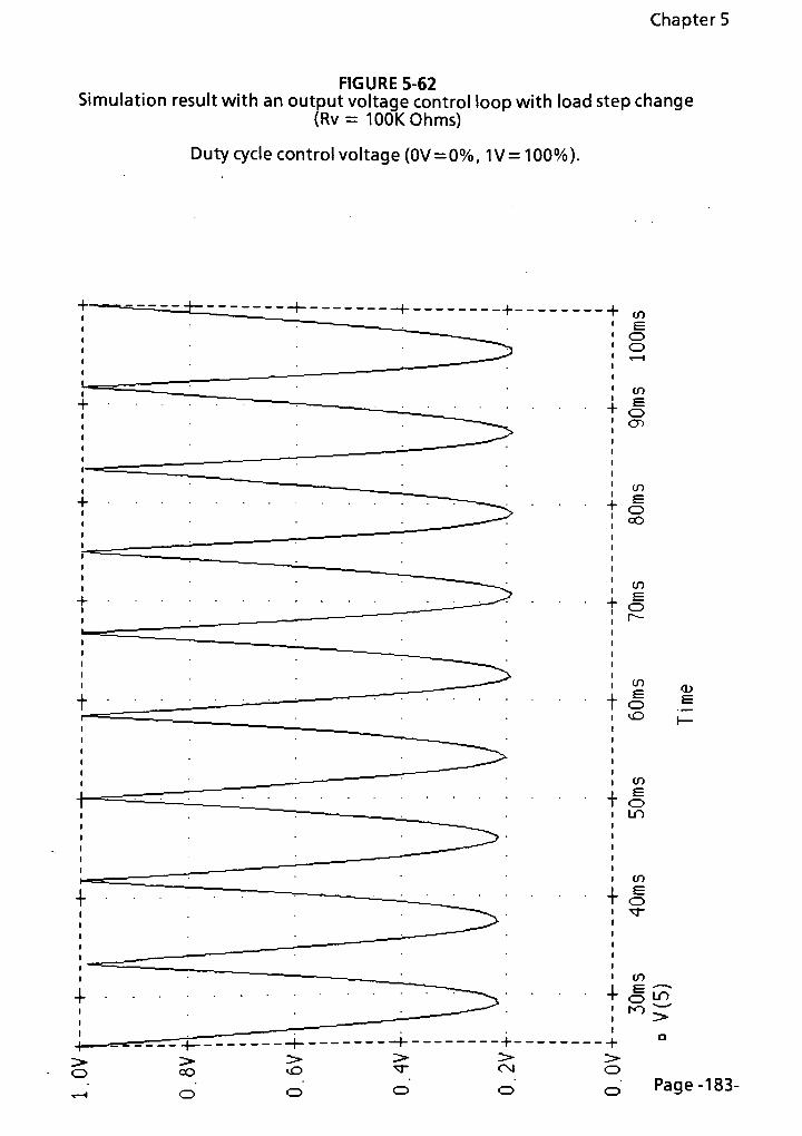
Chapters
FIGURE 5-62
Simulation result with an output voltage control loop with load step change(Rv= 100KOhms)
Duty cycle control voltage (0V= 0%, 1V= 100%).
CD
O
oPage -183-
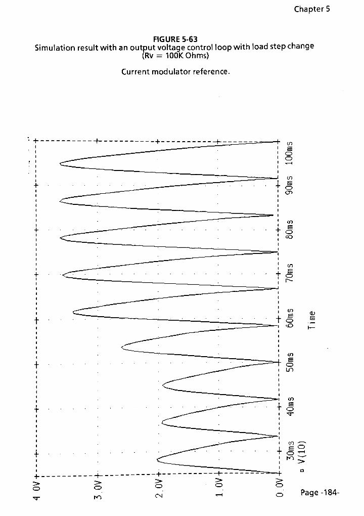
Chapters
FIGURE 5-63
Simulation result with an output voltage control loop with load step change(RV= 100KOhms)
Current modulator reference.
CD
Page -184-

Chapter 5
FIGURE 5-64
Simulation result with an output voltage control loop with load step change(Rv= 100KOhms)
Voltage error amplifier output.
CD
Page -185-

Chapter 5
5.5 SIMULATION OF PFC BOOST CONVERTER SMALL SIGNAL RESPONSE :
The PSPICE model of Figure 5-44 is modified to simulate the small signal
characteristics of the PFC Boost Converter. The sinusoidal input source Vin is replaced
by a DC source with magnitude equal to the RMS value of the sinusoidal source. An
AC source is inserted in series with Rdivl and the output node (4) to provide the AC
stimulus for the simulation. A new node, 4x, is created by the insertion of the AC
source. The control to output frequency response of the control loop, described by
equation (4-91), is measured as the ratio of the converter output (node 4) and the
output of the error amplifier (node 8). The overall loop frequency response is equal
to the ratio of the AC signal at node 4 and the AC signal at node 4x.
The dependence of the control to output frequency response on the RMS magnitude
of the sinusoidal line voltage is illustrated from the simulation results of Figures 5-63
to 5-68. Figure 5-65 is the control to output frequency response with input source
set to an equivalent of 115Vrms. Figure 5-66 is the control to output frequency
response with input source set to an equivalent of 230Vrms. The DC gain with input
of 230Vrms is about 1 2db higher then when input is set to 1 1 5Vrms. This is consistent
with the behavior described by equation (4-91) where the DC gain varies in
proportion to the square of the input voltage. The simulated result also illustrate the
single pole frequency response with the pole frequency determined by R0 and C0-
The 3db frequency of the simulated control to output response is about 2HZ which is
consistent with equation (4-91). The phase characteristic of the control to output
response is displayed in Figure 5-67. The phase characteristic is also consistentwith a
single pole frequency response system where45
phase shift occurs at 2HZ and
maximum phase shift is 90. The overall control loop frequency response simulation
result is displayed in Figure 5-68 for both equivalent input magnitudes of 1 1 5Vrms
and 230Vrms. The zero gain bandwidth when input is set to1 1 5Vrms is 1 /4 of the
bandwidth with the input set to 230Vrms. This result is in accordance with results
predicted by equation (4-91).
Figures 5-69 to 5-72 are simulation results with three gain settings for the voltage
error amplifier. Figure 5-69 displaysthe inductor current for Rv values of 200K Ohms,
100K Ohms and 50K Ohms. The amount of distortion increases as thevalue of Rv
increases. In Figure 5-70 the AC ripples at the output of the error amplifier for the
three Rv values are displayed. With Rv of 50K Ohms, the AC peak to peak ripple at
Page -186-

Chapters
the output of the error amplifier is about 0.45V. With Rv increased to 200K Ohms the
AC peak to peak ripple at the output of the error amplifier is increased to almost
1 .8V. The higher Rv value provides higher amplifier gain which injects greater
amount of AC ripple into the control loop.
The values of Rdivl, Rdiv2 and Vref set the steady state output of the converter to
about 400VDC. When the loop gain is increased the loop is more able to minimize
the steady state error at the output of the converter. Figure 5-71 displays the
converter output for the three Rv values. The output voltage plot with Rv value of
50K Ohms is about 430VDC while the output voltage plot with Rv value of 200K
Ohms is about 400VDC.
Figure 5-72 displays the overall control loop response with three Rv values. The gain
curve with Rv set to 200K Ohms has DC gain of approximately 28db while the gain
curve with Rv set to 50K Ohms has DC gain of approximately 1 6db. The attenuation
of the control loop at 1 20HZ is about 20db for Rv of 50K Ohms and decreases to
about 7db for Rv of 200K ohms. The differences is consistent with the 4 to 1 expected
differences in the AC ripple peak to peak amplitude displayed in Figure 5-70.
Page -187-

Chapters
FIGURE 5-65
Frequency response simulation result(Rv= 100KOhms)
Control to output gain with input equivalent of 1 15Vrms.
4-
+
+
T
t
Oo
o
CD
CT
<D
t
oto
oCM
-+-
o
I
<3>
oO
jQ
>
ITi
-Q
>
-+ O"
oO
7 Page -188-

Chapters
FIGURE 5-66
Frequency response simulation result(Rv= 100KOhms)
Control to output gain with input equivalent of 230Vrms.
Page -189-

Chapter 5
FIGURE 5-67
Frequency response simulation result(Rv = 100KOhms)
Control to output phase with input equivalent of 1 1 5/230 Vrms.
t+_
+
-r
+ + 2
t
oo
=
<D
<D
t
CO
Q.>
t
a.>
+-
o
o oCM
I
o
I
o
o
I
-+-
TD
OCO
I
-+ o
o'
o Page -190-

Chapters
FIGURE 5-68
Frequency response simulation result(Rv= 100KOhms)
Overall control to output gain with input equivalent of 1 1 5/230 Vrms.
to to to
LU
LO
LU
CO
LU
to
to
LOro
oO
1
to
LO
r-
cO
to
Ol
CM
LO
to
cr>
1
n II II
<_>
CM
LJ "O
a
CD
cr
CD
Page -191-

Chapter 5
FIGURE 5-69
Frequency response simulation result
(Vin = 230Vrms)
Top Plot: Inductor currentwith Rv = 50KOhms.
Middle plot: Inductor current with Rv = 100K Ohms.
Bottom Plot: Inductor currentwith Rv = 200KOhms.
CD
Page -192-

Chapters
FIGURE 5-70
Frequency response simulation result(Vin = 230Vrms)
Top Plot: Voltage error amplifier outputwith Rv = 50K Ohms.
Middle plot: Voltage error amplifier outputwith Rv = 100KOhms.
Bottom Plot: Voltage error amplifier output with Rv = 200K Ohms.
<D
- Page -193-

Chapter 5
FIGURE 5-71
Frequency response simulation result
(Vin = 230Vrms)
Top Plot: Converter output voltagewith Rv = 50K Ohms.
Middle plot: Converter output voltage with Rv = 100K Ohms.
Bottom Plot: Converter output voltage with Rv = 200K Ohms.
t <"
<D
Page -194-

Chapter 5
FIGURE 5-72
Frequency response simulation result
(Vin = 230Vrms)
Overall control to output gain with Rv = 50K/100K/200K Ohms.
Page -195-

Chapter 5
5.6 PFC BOOST CONVERTER EXPERIMENTAL CIRCUITDESCRIPTION :
The circuit and data used for experimental verification is based on the circuit and
data published in reference [27] and [28]. The circuit schematics is reproduced in
Figure 5-73 and Figure 5-74.
The schematic of Figure 5-73 is the power processor portion of the experimental pfc
Boost Converter. The schematic of Figure 5-74 is the control circuit portion of the
experimental pfc Boost Converter. The control circuit was implemented based on
Microlinear ML4812 integrated circuit.
The component values listed was chosen based on derivations provided in reference
[28]. The Boost Converter operates at 100KHZ switching frequency. The current in
the inductor is sensed during the ON time of the power switch with the current
transformer T1. The power switches are two parallel connected MOSFETsQI and Q2.
The output capacitors are the series connected capacitors C10 and C1 1 . C8, C9 and
C12 provides high frequency filtering at output DC voltage Vo. The input fullwave
rectified voltage is used as the reference input at node Vs. Vs is then converted into a
current signal by the resistor Rp. The inputs to the multiplier are the output of the
voltage error amplifier and the converted signal from Vs. Both multiplier inputs are
converted current signals. The slope compensation of the current modulation loop is
provided at the input to the PWM comparator at the collector of Q1 in Figure 4-74.
The compensation slope is chosen to equal to 60% of the worst case negative going
slope of the inductor current. The output of the current transformer T1 is converted
into a voltage signal by Rsand connected to anotherterminal of the PWM
comparator. The remaining input of the PWM comparator is connected to 5V and it
is used as the peak current limiting signal not involved with the PFC operation. The
experimental control circuit implemented with ML4812 is the peak current control
current modulator discussed in section 4-8 and illustrated in Figure 4-10.
Page -196-
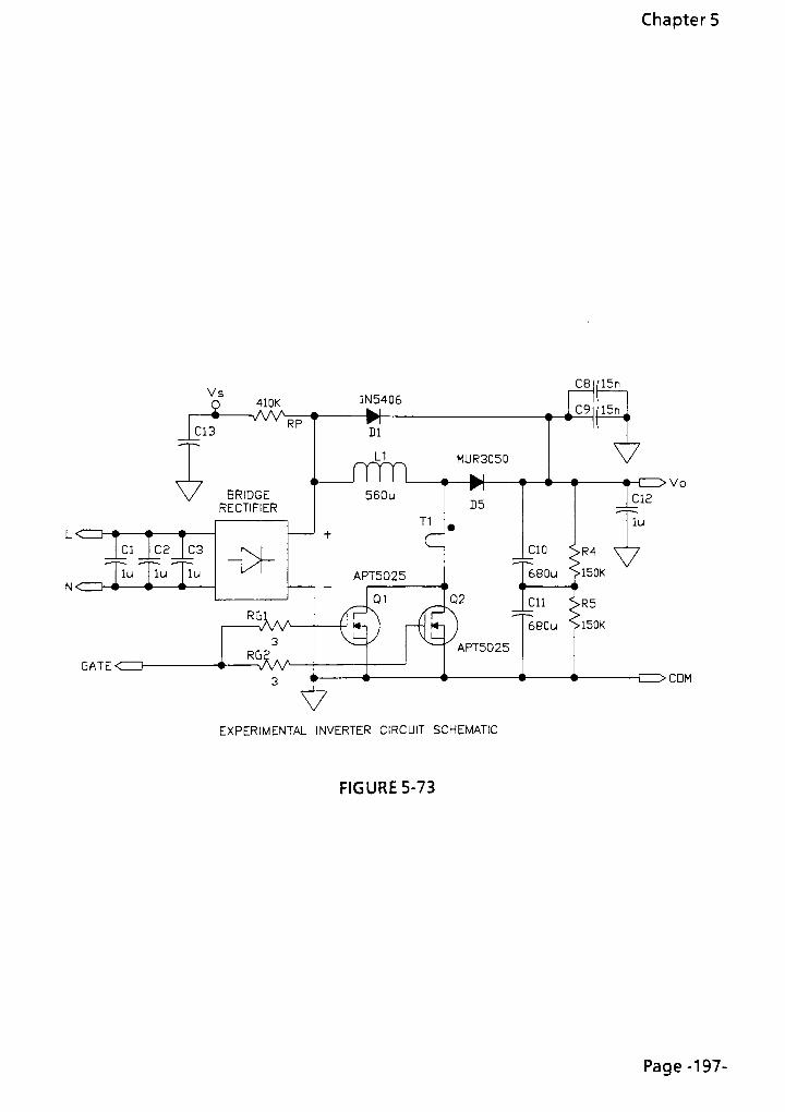
Chapter 5
Vs
-2-
410K
-vVv*
C13RP
1N5406
-w
DI
LI MUR3050
560u
C8|/15n
C9|/15n
CIO SR4
680u >150K
Cll SR5
680u >150K
GATE
EXPERIMENTAL INVERTER CIRCUIT SCHEMATIC
FIGURE 5-73
Vo
C12
lu
CDM
Page -197-
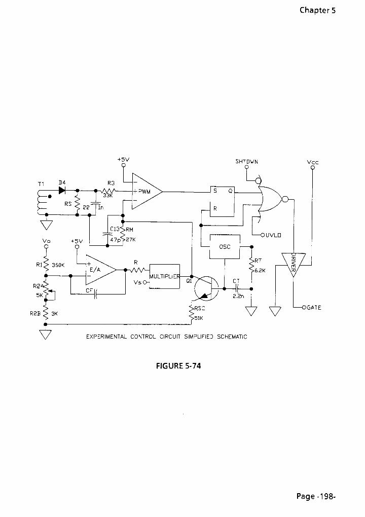
+5V
O
T1 D4
-?f
RS22
Vo +5V
Q
R3
In
C13SRM
47p>27K
Rl> 360KR
VsO
CF
Chapter 5
SHTDWN
O
Vcc
o
MULTIPLIER'
S Q
OSC
R2B > 3K
>UVLD
CT
2,2n
RT
6.3K
EXPERIMENTAL CONTROL CIRCUIT SIMPLIFIED SCHEMATIC
FIGURE 5-74
)GATE
Page -198-

Chapter 5
5.7 PFC BOOST CONVERTER EXPERIMENTAL CIRCUIT RESULTS :
The data provided in references [27] and [28] is used to verify the derivations and
PSPICE simulations. The current modulator control circuit implemented by the
experimental circuit is based on the peak value of the inductor current signal.
Equation (4-50) is the derived governing equation for the peak current controlled
current modulator. The term KR is adjusted by the voltage control loop to to
accomplish voltage regulation. Rearranging equation (4-50) to solve for KR:
m T'
V sini$) Tmc^S
R~
Vjini$)
~
2LVQ
"""
2L
~
VQ
The maximum steady state duty cycle, DMax, is solved by substituting the expression
iorKR into the equation (4-47).
KR and DMax uniquely characterizes the large signal pfcresponses of the Boost
Converter. Using the dwell angle values provided in reference [27], KR and DMax is
calculated and listed in Table 5-5. The other pertinent data are mc- 360K, l =
566uif, Ts = 10us and v0 = 385VDC.
As expected, KR and DMax is proportional to inputpower and inversely proportional
to input voltage.
Page -199-

TABLE 5-5
CALCULATION OF KR AND DMaz FROM EXPERIMENTAL DATA.
Chapter 5
ACTUAL EXPERIMENTAL DATA
INPUT
POWER
(WATTS)
INPUT
VOLTAGE
Vrms (DEGREE)KR
MAX.
DUTY
CYCLE
742 120 11.8 0.1022 0.910
615 120 13.7 0.0880 0.895
488 120 17.6 0.0683 0.866
365 120 21.9 0.0548 0.835
706 240 20.0'
0.0309 0.724
588 240 21.0 0.0292 0.711
469 240 24.0 0.0250 0.671
352 240 30.0 0.0191 0.596
CALCULATED DATA
Page -200-

Chapter 5
The PSPICE circuit model of Figure 5-23 and listed in Table 5-3 is modified to include
the KR values calculated in table 5-5. The output load resistance was changed to
match the input power magnitude listed in Table 5-5. The simulation results are
presented in Figures 5-75 to 5-86.
Figures 5-75 to 5-78 displays the simulated inductor current waveform for the
various power levels and with input voltage of 230Vrms. The dwell angles in the
inductor current agrees with the experimentally measured data. Figures 5-79 and5-
80 displays the simulated duty cycle signal variations. The maximum steady state
duty cycle signal values also agrees with theDMax values listed in Table 5-5.
Figures 5-81 to 5-84 displays the simulated inductor current waveform for the
various power levels and with input voltage of 120Vrms. The dwell angles in the
inductor current agrees with the experimentally measured data. Figures 5-85 and5-
86 displays the simulated duty cycle signal variations. The maximum steady state
duty cycle signal values also agrees with the DMax values listed in Table 5-5.
The PF and THD of the experimental circuit is calculated with equation (4-60) and (1-
17) respectively. Alternatively the PF and THD can be determined from the curves
displayed in Figures 4-14 and 4-15.
The experimental verification results is summarized in Tables 5-6 and 5-7.
Page -201
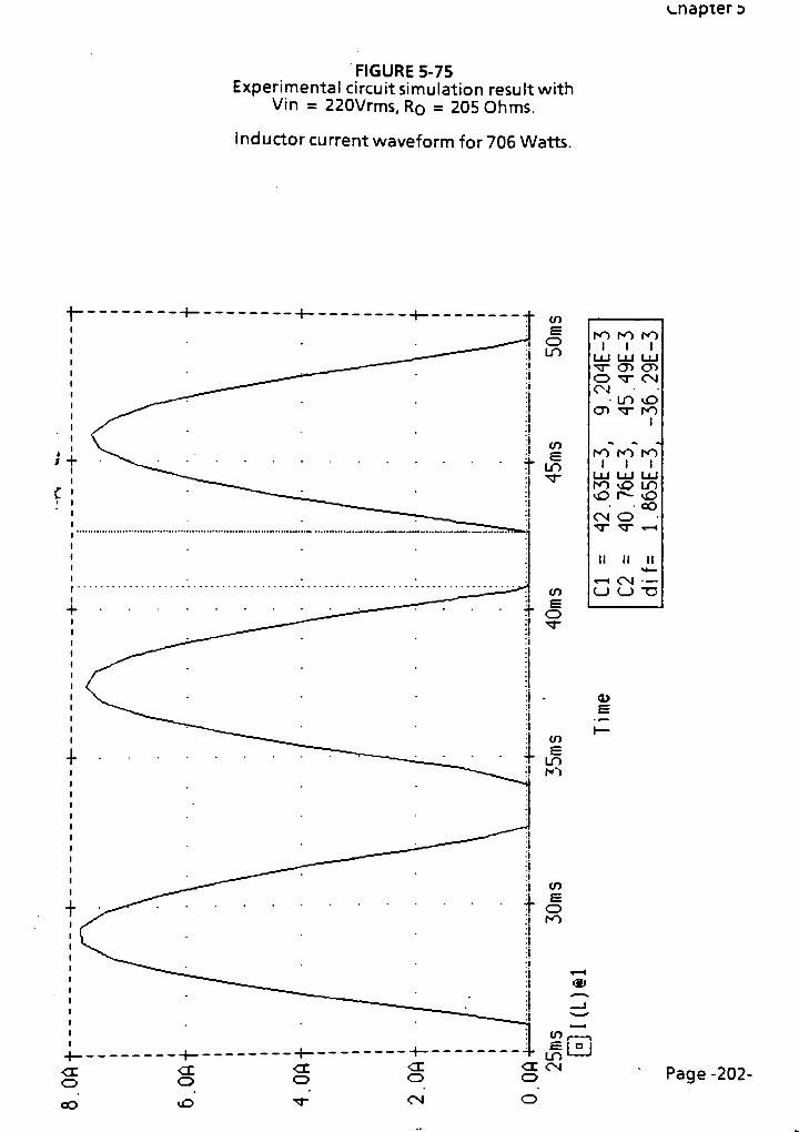
FIGURE 5-75
Experimental circuit simulation resultwithVin = 220Vrms,Ro = 205 Ohms.
Inductor currentwaveform for 706 Watts.
L,napter:>
ro ro to
LU LU LU
<r CD CT>
o T CM
OJ
LO <JD
cr> ^r to
1
. .
ro ro to
LU LU LU
ro vO LO
o r cO
CO
CM o
TT<T-
* t
II II II
1t CM
LJ LJ o
CD
Page -202-

FIGURE 5-76Experimental circuit simulation resultwith
Vin = 220Vrms, R0 = 246 Ohms.
Inductor currentwaveform for 588Watts.
L.napxer o
o <iD cn
LU LU LU
CD CM CO
CM to
ro OCO
""H T 1 cm
,
ro ro to
LU LU LUCM CD roro TT CM
cr>
ST CM
ro to """'
n II n
i CM ._
LJ LJ o
CD
Page -203-

FIGURE 5-77
Experimental circuit simulation resultwithVin = 220Vrms,Ro = 308 Ohms.
Inductor currentwaveform for 469 Watts.
cnapter :>
cr> <T> cr>
LU
to
LU
CD
LU
DO
CMcr>
r-
CMcr>
CD
I
ro ro ro
LU
CM
ro
to
LU
LO
CM
CM
to
LUt
r-
CD
CM
n II II
CM
LJ o
CD
Page -204-

Chapter 5
FIGURE 5-78Experimental circuit simulation result with
Vin =
220Vrms,Ro = 410 Ohms.
Inductor current waveform for 352Watts.
ro to toi i i
LU LU LU^h CD P-
HOO
I
CM CM LO
.
ro
i
to to
LU LU LUo T ( T
CO to cr>
sr
CM CDT t CM
11 n u
t CM ._
LJ LJ o
<D
LO ro CM
Page -205-

unapter o
FIGURE 5-79
Experimental circuit simulation resultwith
Vin = 220Vrms
Top Plot: Duty cycle signal for Ro = 205 Ohms.
Bottom Plot: Duty cycle signal for Rq = 246 Ohms.
CD
Page -206-

v_iidpie( o
FIGURE 5-80Experimental circuit simulation resultwith
Vin = 220Vrms
Top Plot: Duty cycle signal for R0 = 308 Ohms.Bottom Plot: Duty cycle signal for R0 = 410 Ohms.
CD
CD
O
CD
CD
o
o
CD
CD
CD
O
Ol
Page -207-

FIGURE 5-81Experimental circuit simulation resultwith
Vin = 120Vrms,Ro = 195 Ohms.
Inductor current waveform for 742Watts.
LnajJici J
I
^O CD
LU LU LUCD CO oCO to CM
to to
CDCM CM LO
.
to
1
to1
ro1
LU LU LUCD CO r-
oO r^- T<
ro CMto to T-
n n II
t CM
LJ LJ TD
CD
Page -208-
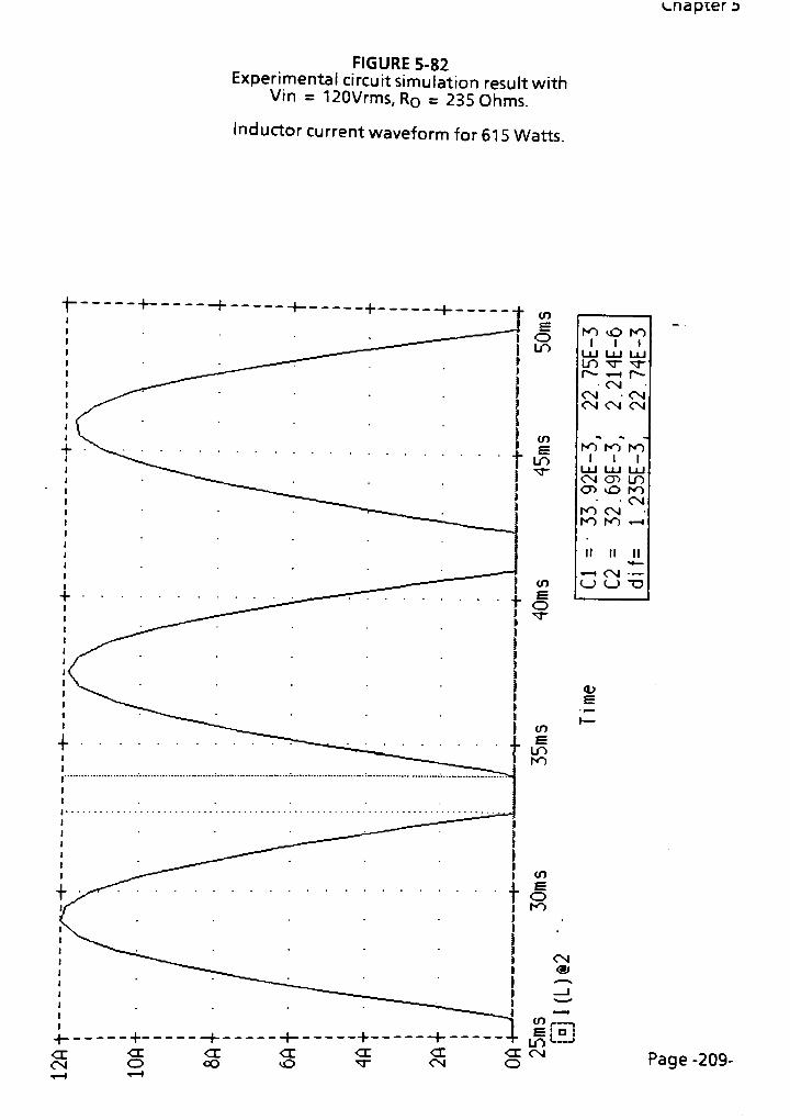
cnapxer 5
FIGURE 5-82Experimental circuit simulation resultwith
Vin = 120VrmsfRo = 235 Ohms.
Inductor currentwaveform for 61 5 Watts.
to O ro
LU LU LU
LO ^rT-
r-
o>i
r-
CM CMCM CM CM
,
ro ro to
LU LU LU
CM cr> lOCD kO ro
CMro OnI
ro to
u il n
^i CM ._
LJ LJ 10
CD
Page -209-

L,napier o
FIGURE 5-83Experimental circuit simulation resultwith
Vin = 120Vrms,Ro = 296 Ohms.
Inductor current waveform for 488Watts.
ro to to
i i i
LU LU LU
CD co or- LO CM
cO <CD
ro ro to
i i i
LU LU LU
TtOOr-4 LO
<r cm
ro ro ^
ii it u
LJ LJ TD
Page -210-

FIGURE 5-84
Experimental circuit simulation resultwith
Vin = 120Vrms,Ro = 396 Ohms.
Inductor current waveform for 365Watts.
v_napiet d
to to ro
LU
CD
CM
LUCD
LU
CD
LO
CD"3"
to t
to to ro
i
LU
LOCD
CDLO
LU
1
o
CD"3"
LU
toCD
II II II
^H CM
LJ LJ "O
CD
Page-211-

unapxet d
FIGURE 5-85
Experimental circuit simulation resultwith
Vin = 120Vrms
Top Plot: Duty cycle signal for Ro = 195 Ohms.
Bottom Plot: Duty cycle signal for Rq = 235 Ohms.
t
7
+
+
\
I
T
I
CD
<D
Page -212-

FIGURE 5-86
Experimental circuit simulation resultwith
Vin = 120Vrms
Top Plot: Duty cycle signal for Ro = 296 Ohms.
Bottom Plot: Duty cycle signal for Ro = 396 Ohms.
Chapter s
+ to
Page -213-

Chapters
TABLE 5-6
EXPERIMENTAL VERIFICATION RESULT SUMMARY FOR 120Vrms.
EXPERIMENTAL RESULTS CALCULATED/SIMULATED RESULTS
INPUT
POWER
(WATTS)
PFTHD
{%)
0>
(DEGREE)Ro
(OHMS)
PFTHD
{%)
0
(DEGREE)
742 0.991 12.30 11.80
615 0.988 14.36 13.70
488 0.983 16.95 17.60
365 0.976 20.53 21.90
195
235
296
396
0.9911
0.9890
0.9810
0.9720
13.45
14.94
19.19
24.17
12.064
13.338
17.388
20.920
TABLE 5-7
EXPERIMENTAL VERIFICATION RESULT SUMMARY FOR 220Vrms.
EXPERIMENTAL RESULTS
INPUT
POWER
(WATTS)
706
588
469
352
PF
0.976
0.969
0.958
0.940
THD
(%)
19.93
22.83
25.73
31.10
CD
(DEGREE)
20.00
21.00
24.00
30.00
CALCULATED/SIMULATED RESULTS
Ro(OHMS)
PFTHD
(%) (DEGREE)
205 0.9741 23.19 20.142
246 0.9724 23.98 20.768
308 0.9678 26.01 22.367
410 0.9523 32.04 26.935
Page -214-

Conclusions
CONCLUSIONS
The need for power factor correction of off line power converterswith capacitive
input filter has been established, pfc is necessary to increase the utilization
efficiency of the AC power and to minimize harmonic pollution of the AC lines. The
future adaptation of IEC-555 standard, stipulating the requirement for harmonic
magnitudes, is an additional impetus for implementing pfc across a broad base of
applications.When the regulatory standards are formalized, many of the office
equipments such as work stations, copiers, printers and computers of all sorts will be
held responsible for the current waveshape at its input terminals.
Passive methods of pfc are simplistic and effective. The two passive pfc networks
discussed in this Thesis, the inductive input filter and the resonant input filter, both
have been shown to be capable of improving power factor by eliminating the high
order harmonics from the currentwaveform. In the analysis of the inductive input
filter, the theoretical maximum PFachievable is calculated to be about 0.9. The
resonant input filter is theoretically capable of achieving unity pfwhen the resonant
frequency of the filter is tuned to the frequency of the AC line. The reactive elements
of the passive pfc networks must be designed for line frequency operation. The
resultant large and heavy reactive elements are unattractive for use in office
equipmentswhere the trends has been toward miniaturization.
Active power processors, based on switching converters or resonant converters, can
also be specially designed to"shape"
the line input current while operating at
frequencies orders of magnitudes above the line frequency. The high frequency
operation makes it possible to use very small and light weight reactive elements in its
design. The reduced size and weight must be balanced against the additional parts
and complexity associated withan active power processors.
A PFC Boost Converter is analyzed in detail for two methods of implementing the
current modulator controller. The two currentmodulator controllers are specified as
the peak current controller and the averagecurrent controller. Both current
modulators reshape the average input current of thePFCConverter into a scaled
replica of the fullwave rectified input voltagewaveform. The current waveform of
both current modulator controllers exhibitsdistortions at or near the zero crossings
of the voltage waveform. The source ofthe current waveform distortions for the
Page -215-

Conclusions
two currentmodulator controllers are different and they are treated separately in
detail in the Thesis.
The pfc function effectively forces the input port of the Boost Converter to appear
as a resistor. The effective value of the resistor is derived and is designated as REff.
The dynamicmagnitude of REff\s a function of the duty cycle and the output DC load
of the pfcConverter.
The distortion of the input current waveform for a pfcConverter implementing the
average current controller is attributed to delay intervalswhere the inductor current
lags the voltage waveform at or near the zero crossings. The delay is present because
the finite dildt of the inductor current is unable to match the dvldt of the voltage
waveform at and near the zero crossings. The delay interval distortion is minimized
by lowering the value of the inductorwhich increase the dildt response of the
inductor current.
The distortion of the input currentwaveform for a PFCConverter implementing the
peak current controller is attributed to dwell intervalswhere the inductor current is
zero. The dwell intervals in the inductor current is attributed to the current
controller responding to the peak value of the inductor current while attempting to
control the average value of the inductor current. The dwell interval distortion is
minimized by increasing the value of the inductor which reduces the differences
between the peak and average value of the inductor current.
The dwell interval is also affected by the compensation slope which is required to
avoid subharmonic oscillations when the duty cycle exceeds 50% . The compensation
slope increase the differences between the peak and average inductor current signal
in the controller and results in a longer dwell interval.
Both types of current controller shape the average current waveform of the input
current. For both current controllers discussed in the Thesis, the pfc Boost Converter
can be modeled as a controlled current source driving the output impedance of the
converter. The DC power consumed by the output load is reflected into the input
port as an effective resistor. The PFC BoostConverter inherently behaves as a
constant power converter. The output voltageof the converter can be regulated by
controlling the magnitudeof the current source driving the output port of the
converter.With the output voltage held to a constant value, the converter will force
Page -216-
the current source to beinversely proportional to the input voltage magnitude and
directly proportional to the output load power. The signal level of the current
reference for the current controller is dynamically adjusted to maintain the current
source magnitude at a level required to regulate the output voltage.
It is necessary to limit the response of the voltage control loop to be insensitive to
the AC ripples on the output capacitor. This mean the voltage control loop
bandwidth must be limited to below the ripple frequency of the capacitor. If not
properly attenuated, the AC ripple on the output capacitor can be injected into the
voltage control loop and be superimposed on the current controller reference signal.
The AC ripple signal will then introduce distortions in the input current waveform as
the current controller respond to the AC ripple signal.
The AC ripple signal can be eliminated entirely by preceding the output voltage
sense or after the voltage error amplifier output with a sample and hold circuit. The
sample and hold circuit is synchronized to the AC ripple frequency preventing the AC
ripples from being sensed and subsequently injected into the control loop.
The gain of the small signal model for the pfc converter is derived to be
proportional to the input voltage RMS value squared. The proportionality term can
be divided out of the loop by the addition of a squarer and divider circuit.
The small signal characteristic of the PFCConverter can be suitably described by a
single pole transfer function.When the converter load is purely resistive, the pole
frequency is set by the output capacitance and 50% of the output load resistance.
When the converter is powering cascaded converters, the negative incremental
input resistance of the cascaded converter cancels the small signal output resistance
of the PFC converter. The response of the converter is determined by the current
source driving into the output capacitance.
The performance of the pfc Boost Converters has been successfully simulated with
PSPICE. The simulation results corresponds with actual experimental results
published in references [27] and [28].
Several pfc controller IC has been introduced in the recent period.Without
exception these controllers are based on analogcircuit techniques. Non-of the
controller has a sample and hold circuit built into the IC. Considering the functions
necessary to implement thePFC controller, it is perhaps more suitable to use a low
end microcontrollerwith built in A/Dconverters and PWM outputs as the PFC
controller. Traditionally low end microcontroller based
Page -217-

Conclusions
power converter controllers can not produce the desirable wide control bandwidth
due to the limitation of calculation speed for real time compensation. Since the PFC
Converter has an inherent bandwidth limitation, a microcontroller is better suited
for functions such as multiplication, squaring and divisions, rms value calculations,
sample and hold sensing much more naturally then analog circuits.
Page -218-

References
REFERENCES
[1] G.W.Wester and R.D. Middlebrook, "Low-Frequency Characterizationof Switching DC-to-DC Converters", IEEE Power Processing andElectronics Specialist Conferences, 1972 Record.
[2] R.D. Middlebrook and Slobodan Cuk, "A General Unified Approach to
Modeling Switching-Converter Power Stages", IEEE Power ElectronicsSpecialist Conference, 1976 Record.
[3] Shi-Ping Hsu, Art Brown, Loman Rensink and R.D. Middlebrook,"Modeling and Analysis of Switching DC-to-DC Converters in
Constant-Frequency Current-Programmed Mode", IEEE PowerElectronics Specialist Conference, 1979 Record.
[4] R.D. Middlebrook, "Topics in Multiple-Loop Regulators and Current-Mode Programming", IEEE Power Electronics Specialist Conference,1985 Record.
[5] R.D. Middlebrook, "Modeling Current-Programmed Buck and Boost
Regulators", Proc. IEEE Transactions on Power Electronics, VOL. 4 NO.
1, January 1989.
[6] Dr. Vincent G. Bello, "Computer-Modeling the Pulse Width
Modulated (PWM) Inverter", Proceeding of POWERCON 7, 1980.
[7] Dr. Vincent G. Bello, "Using the Spice2 CAD package to simulate and
design the current mode Converter", Proceeding of POWERCON 1 1,
1984.
[8] K. Kit Sum, "Switch Mode Power Conversion", Marcel Dekker, Inc.
Electrical Engineering and Electronics/22, 1984.
[9] Rudolf P. Severns, Gordon E. Bloom, "Modern DC-to-DC Switchmode
Power Converter Circuits", Van Nostrand Reinhold
Electrical/Computer Science and Engineering Series, 1985.
[10] California Institute of Technology Power Electronics Group,"Input-
Current Shaped AC-to-DC Converters", Final Report Prepared for
NASA Lewis Research Center, May 1986.
[11] Lloyd H. Dixon, "High Power Factor Preregulators for Off-Line Power
Supplies", Unitrode Switching Regulator Power Supply Design
Seminal Manual, 1988, 6-1 to 6-16.
[12] C.P. Henze, N. Mohan, "A Digitally Controlled AC to DC Power
Conditioner that draws sinusoidal input current", IEEE Power
Electronics Specialist Conference, 1986 Record.
[13] M. Kazerani, G. Joos, P.D. Ziogas, "Programmable Input Power Factor
Correction Methods for single phase diode rectifier circuits", IEEE
Applied Power Electronics Conference, 1990 Record.
Page -219-

References
[14] Robert Erickson, Michael Madigan, Sigmund Singer, "Design of a
simple High-Power-Factor Rectifier Based on Flyback Converter", IEEE
Applied Power Electronics Conference, 1990 Record.
[1 5] Mark A. Geisler, "Predicting Power Factor and other Input Parametersfor Switching Power Supplies", IEEE Applied Power ElectronicsConference, 1990 Record.
[16] Arthur W. Kelley, William F. Yadusky, "Rectifier Design for minimumLine Current Harmonics and Maximum Power Factor", IEEE Power
Electronics Specialist Conference, 1989 Record.
[17] James B. Williams, "Design of Feedback loops in Unity Power FactorAC to DC Converter", IEEE Applied Power Electronics Conference,1989 Record.
[18] Kwang-Hwa Liu, Yung-Lin Lin, "Currentwaveform distortion in Power
Factor Correction Circuits Employing Discontinuous-Mode Boost
Converters", IEEE Applied Power Electronics Conference, 1989 Record
[19] Alex J. Severinsky, "AC to DC Power Converters with Integrated Line
Current Control for Improving Power Factor", United State Patent
4,816,982, Mar. 28, 1989.
[20] Michika Uesugi, "AC-DC Converting Appratus Having Power Factor
Improving Circuit Utilizing a Photocoupler", United State Patent
4,825,351, Apr. 25, 1989.
[21] Patrick L. Hunter, "Power Supply System Having Improved Input
Power Factor", United State Patent 4,831,508, May 16, 1989.
[22] Neil Kammiller, "Power Factor Correction Circuit", United State
Patent 4,855,890, Aug. 8, 1989.
[23] Frank Cover, "Power Factor Corrector", United State Patent 4,876,497,
Oct. 24, 1989.
[24] Cecil W. Deisch, "Power Factor Improving Arrangement", United State
Patent 4,914,559, Apr. 3, 1990.
[25] William F. Slack, James C. Wedlington, "Method and Network for
Enhancing Power Factor of Off-Line Switching Circuit",United State
Patent 4,930, 061, may 29, 1990.
[26] MehmetK. Nalbant, "Power Factor Calculation and Measurements",
IEEE Applied Power Electronics Conference, 1990 Record.
[27] ML481 2 data sheet, Microlinear Corportion.
[281 Mehmet K. Nalbant, Jon Klein, "Design of a 1 KW Power Factor
Correction Circuit",PGM July 1990 pp17-pp24.
[29] PSPICE User's manual.
[30] Benjamin C. Kuo, "Automatic Control Systems",5th Edition, Prentic
Hall 1987.
Page -220-

References
[31] MC68HC05B5 User's Manual, Motorola Corporation.
[32] Signetics Microcontroller User's Guide, Philips Corporation.
[33] Single-Chip 8-Bit Microcontrollers PCB83C552/562 users Manual 1989,Philips Corporation.
Page -221-