Analysis of InGaAs/InAlAs Optoelectronic Mixers for … · Analysis of InGaAs/InAlAs Optoelectronic...
22
Analysis of InGaAs/InAlAs Optoelectronic Mixers for Fuze and LADAR by Neal K. Bambha, Justin R. Bickford, Stephen Drew, and Nuri W. Emanetoglu ARL-TR-5071 March 2010 Approved for public release; distribution unlimited.
Transcript of Analysis of InGaAs/InAlAs Optoelectronic Mixers for … · Analysis of InGaAs/InAlAs Optoelectronic...

Analysis of InGaAs/InAlAs Optoelectronic Mixers for Fuze
and LADAR
by Neal K. Bambha, Justin R. Bickford, Stephen Drew, and Nuri W. Emanetoglu
ARL-TR-5071 March 2010 Approved for public release; distribution unlimited.

NOTICES
Disclaimers The findings in this report are not to be construed as an official Department of the Army position unless so designated by other authorized documents. Citation of manufacturer’s or trade names does not constitute an official endorsement or approval of the use thereof. Destroy this report when it is no longer needed. Do not return it to the originator.

Army Research Laboratory Adelphi, MD 20783-1197
ARL-TR-5071 March 2010 Analysis of InGaAs/InAlAs Optoelectronic Mixers for Fuze
and LADAR
Neal K. Bambha, Justin R. Bickford, Stephen Drew, and Nuri W. Emanetoglu
Sensors and Electron Devices Directorate, ARL Approved for public release; distribution unlimited.

ii
REPORT DOCUMENTATION PAGE Form Approved OMB No. 0704-0188
Public reporting burden for this collection of information is estimated to average 1 hour per response, including the time for reviewing instructions, searching existing data sources, gathering and maintaining the data needed, and completing and reviewing the collection information. Send comments regarding this burden estimate or any other aspect of this collection of information, including suggestions for reducing the burden, to Department of Defense, Washington Headquarters Services, Directorate for Information Operations and Reports (0704-0188), 1215 Jefferson Davis Highway, Suite 1204, Arlington, VA 22202-4302. Respondents should be aware that notwithstanding any other provision of law, no person shall be subject to any penalty for failing to comply with a collection of information if it does not display a currently valid OMB control number. PLEASE DO NOT RETURN YOUR FORM TO THE ABOVE ADDRESS.
1. REPORT DATE (DD-MM-YYYY)
March 2010 2. REPORT TYPE
3. DATES COVERED (From - To)
4. TITLE AND SUBTITLE
Analysis of InGaAs/InAlAs Optoelectronic Mixers for Fuze and LADAR 5a. CONTRACT NUMBER
5b. GRANT NUMBER
5c. PROGRAM ELEMENT NUMBER
6. AUTHOR(S)
Neal K. Bambha, Justin R. Bickford, Stephen Drew, and Nuri W. Emanetgolua 5d. PROJECT NUMBER
5e. TASK NUMBER
5f. WORK UNIT NUMBER
7. PERFORMING ORGANIZATION NAME(S) AND ADDRESS(ES)
U.S. Army Research Laboratory Attn: RDRL-SEE-M 2800 Powder Mill Road Adelphi, MD 29783-1197
8. PERFORMING ORGANIZATION REPORT NUMBER
ARL-TR-5071
9. SPONSORING/MONITORING AGENCY NAME(S) AND ADDRESS(ES)
10. SPONSOR/MONITOR’S ACRONYM(S) 11. SPONSOR/MONITOR'S REPORT NUMBER(S)
12. DISTRIBUTION/AVAILABILITY STATEMENT
Approved for public release; distribution unlimited.
13. SUPPLEMENTARY NOTES
14. ABSTRACT
We are developing a symmetric gain optoelectronic mixer for chirped-FM laser detection and ranging systems (LADAR) operating in the 1.55 μm wavelength range. Signal processing of a chirped-FM LADAR system is simplified if the photodetector in the receiver is used as an optoelectronic mixer (OEM). Adding gain to the optoelectronic mixer allows a reduction of the following transimpedance amplifier’s gain, increasing bandwidth and improving the system’s noise performance. The symmetric gain optoelectronic mixer is based on a symmetric heterojunction phototransistor. The base layer is indium gallium arsenide (In0.53Ga0.47As), and the emitter/collector layer is In0.48Al0.52As. Two-dimensional simulations of the devices were carried out to analyze device performance. Two sample heterostructures were grown using molecular beam epitaxy. We are currently in the prototype development stage. Simulation results and preliminary results from the initial batch of devices are presented. These symmetric gain optoelectronic mixer devices can lead to a miniaturized LADAR-on-chip system. Such a system will have many military and civilian applications, such as range finding, terrain mapping, reconnaissance, and face recognition. 15. SUBJECT TERMS
LADAR, FUZE, photodetector
16. SECURITY CLASSIFICATION OF: 17. LIMITATION
OF ABSTRACT
UU
18. NUMBER OF PAGES
22
19a. NAME OF RESPONSIBLE PERSON Neal K. Bambha
a. REPORT
Unclassified b. ABSTRACT
Unclassified c. THIS PAGE
Unclassified 19b. TELEPHONE NUMBER (Include area code) (301) 394-4161
Standard Form 298 (Rev. 8/98) Prescribed by ANSI Std. Z39.18

iii
Contents
List of Figures iv
List of Tables iv
Acknowledgments v
1. Introduction 1
2. Simulation Study and Device Design 3
3. Material Growth and Device Fabridcation 7
4. Experimental Results 8
5. Conclusions 9
6. References 10
Symbols, Abbreviations, and Acronyms 12
Distribution List 13

iv
List of Figures
Figure 1. Schematic structure of basic symmetric gain optoelectronic mixer. ...............................2
Figure 2. DC responsivity of a sample OEM device, simulated with SimWindows. ......................3
Figure 3. Predicted mixing responsivity vs. LO voltage for the device of figure 2.........................4
Figure 4. Vertical structure of the two samples selected for material growth and device fabrication. .................................................................................................................................4
Figure 5. Current density distribution in a device with the Sample 1 layer structure. .....................5
Figure 6. Simulated I-V characteristics of an SG-0EM device on sample 1, using TCAD-Sentaurus. ...................................................................................................................................6
Figure 8. Comparison of I-V characteristics for an ‘ideal’ 1D SG-OEM device and an ‘actual’ 2D device showing the effect of the bottom contact placements on SG-OEM device performance ....................................................................................................................7
Figure 9. Top-view photograph of a prototype symmetric gain optoelectronic mixer. ...................7
Figure 10. I-V curves for top- (red) and back-side (blue) illumination devices with r = 9 µm. .....8
List of Tables
Table 1. Simulated device parameters .............................................................................................5

v
Acknowledgments
We acknowledge Paul H. Shen and Wayne Chang for discussions regarding device design and development, and Stefan Svenson for growing the heterostructure samples. This research was partially funded by the U.S. Army Research Office/Laboratory (ARL) through a Scientific and Technical Services Agreement issued by Battelle Chapel Hill Operations, TCN 07-058 under contract W911NF-07-D-0001.

vi
INTENTIONALLY LEFT BLANK.
1
1. Introduction
The U.S. Army Research Laboratory (ARL) has been developing chirped-FM laser detection and ranging (LADAR) systems for applications such as reconnaissance, terrain mapping, force protection, facial recognition, robotic navigation, and weapons fuzing. Signal processing of a chirped-FM LADAR system is simplified if the photodetector in the receiver is used as an optoelectronic mixer (OEM) [Ruff, et al. 2000]. A symmetric I-V characteristic photodetector can be used as an OEM. This allows the OEM to be driven directly with the local oscillator (LO) signal, without a direct current (DC) bias. Sensitivity to background light is reduced, as the response from background light averages to zero. An additional 3 dB signal processing gain is also obtained. The OEM output is the low frequency difference signal—several orders of magnitude lower than the LO signal. Therefore, the gain of the transimpedance amplifier (TZA) following the photodetector can be increased, improving LADAR range. The metal-semiconductor-metal (MSM) Schottky detector is such a symmetric device. ARL has previously demonstrated chirped FM LADAR systems with gallium arsenide (GaAs) and indium gallium arsenide (InGaAs) MSM OEMs for operation at the 800 nm [Ruff, et al. 2000, Shen et al. 2002] and 1550 nm [Shen, et al. 2003, Shen et al. 2004] wavelengths.
A symmetric photodetector with gain would improve overall system performance, while preserving the advantages offered by MSM OEM devices. An OEM with gain would allow the gain of the following transimpedance amplifier to be reduced, increasing the TZA frequency bandwidth and improving overall system performance. Such a device can be based on the heterojunction phototransistor (HPT) or the modulated barrier diode (MBD), also known as a Camel diode.
The basic HPT is a two terminal device, with the emitter made of a semiconductor that has a wider bandgap than the base and collector regions. A number of modifications to the basic HPT structure have been investigated to improve performance. A base bias can be provided, either optically or by an electrical contact [Chandrasekhar, et al. 1991]. The base composition can be graded to establish an electric field, which enhances electron transport [Capasso, et al. 1983, Thuret, et al. 1999]. Improvements in material growth, device design, and fabrication techniques have increased the maximum bandwidth of HPTs to the tens of GHz range [Choi, et al. 2005, Polleux, et al. 2004]. HPT responsivity typically increases with increasing optical power. This has been attributed to recombination at the base-emitter heterojunction. It is desirable to have gain independent from the optical power, or have larger gain at lower optical power levels. One approach to improve the gain dependence on optical power is to adjust the doping profile of the emitter and base layers of indium phosphide (InP) emitter/InGaAs base HPTs [Lue, et al. 1991]. By reducing the emitter doping in a thin layer at the emitter-base junction, the quantum well trapping of the electrons at this interface was reduced. The recombination currents were thus reduced, and the ideality factor of the transistor improved, leading to a flattening of the gain versus incident power characteristics. HPTs have been demonstrated for optoelectronic mixing applications, where the LO signal was provided electrically [Choi, et al. 2005, Liu, et al. 1997] or optically [Van de Casteele, et al., 1996].

2
The MBD, also known as the Camel diode, is a non-Schottky majority carrier diode in which the carrier transport is controlled by a potential barrier in the bulk of the semiconductor. The application of MBDs as photodetectors was first demonstrated by A.Y. Cho and co-workers [Chen, et al. 1981, Chen 1981]. The gain of the MBD is due to the hole trapping at the heterostructure interface. As holes accumulate in this quantum well, the barrier height will be lowered, resulting in an increased electron current, thus providing gain. As a majority carrier device, the MBD has fast intrinsic response [Chen, et al. 1981, Bethea, et al. 1982]. In contrast with the HPT, the MBD device has higher responsivity at lower optical power levels. The MBD has been used in a front-end photoreceiver, integrated with an FET [Li and Bhattacharya, 1989], and a monolithically integrated phototransceiver, in which it was integrated with an LED [Qasaimeh, et al. 2000]. In the first case, the MBD and FET shared a common structure, and the circuit used the MBD’s gain and response speed. In the second case, the MBD’s increasing gain with lower optical power was used to improve optical transceiver performance.
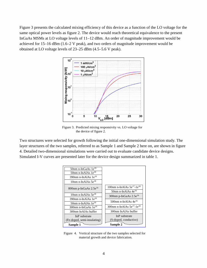
A symmetric gain OEM (SG-OEM) is being investigated in this work, for chirped-AM LADAR applications. The device is based on a symmetric heterostructure, as shown in figure 1. The targeted operating wavelength is 1.55 µm. The emitter/collector is In0.52Al0.48As, and the base is In0.53Ga0.47As, both of which are lattice matched to the InP substrate. Through proper design, particularly of the In0.52Al0.48As E/C layers, the device can have larger gain at lower optical power levels. Initial simulation studies at ARL used the one-dimensional SimWindows program. Two- and three-dimensional device simulations, using the Synopsis TCAD Sentaurus suite, are being carried out at the University of Maine to design OEM with suitable optical gain and frequency bandwidth. Two symmetric gain OEM heterostructures were grown at ARL using molecular beam epitaxy. Sample 1 has a base width of 800 nm and sample 2’s width is 300 nm. Both samples nominally have the same base doping of 2.5x1016 cm–3. Prototype devices were fabricated at the University of Maine, in collaboration with ARL. Device diameters range from 18 µm to 30 µm.
N-InAlAs emitter/ collector
p-InGaAs base
N-InAlAs emitter/ collector
InP
n+-InGaAs contact layer
SI InP substrate
n+-InGaAs contact layer
Figure 1. Schematic structure of basic symmetric gain optoelectronic mixer.

3
2. Simulation Study and Device Design
The initial one-dimensional device simulation study was done using the program SimWindows (copyright: David W. Winston). Both symmetric HPTs and symmetric MBDs were investigated as candidates for the OEM. The effects of the layer thicknesses and doping densities were investigated for the two types of devices, including positional variation of the doping densities. The optimum for both types of devices converged to similar structures. The symmetric HPT based structure was chosen for the symmetric gain OEM.
Two parameters need to be balanced in designing the SG-OEM. First, the responsivity needs to be highly symmetric, with as large a value as possible to make the device a practical alternative to the existing MSM-OEMs. Second, the device should turn on at low voltages to avoid large power dissipation. These two requirements place contradictory constraints on the device design, resulting in a trade off between gain and turn-on voltage, and need to be optimized for specific applications.
The SG-OEM can be designed with a very symmetric responsivity, and the “turn on” voltage can be reduced to below 0.1 V, significantly reducing the voltage swing range for the device. The symmetric OEM behaves similarly to a MBD, in that the gain increases with decreasing optical power. This behavior is shown in figure 2, which presents the simulated DC responsivity curves of a sample device for incident optical powers ranging from 1 µW/cm2 to 1 mW/cm2. The device has a base thickness of 0.2 µm and doping of 1017 cm–3, while the InAlAs layer doping is 4x1016 cm–3.
Figure 2. DC responsivity of a sample OEM device, simulated with SimWindows.
4
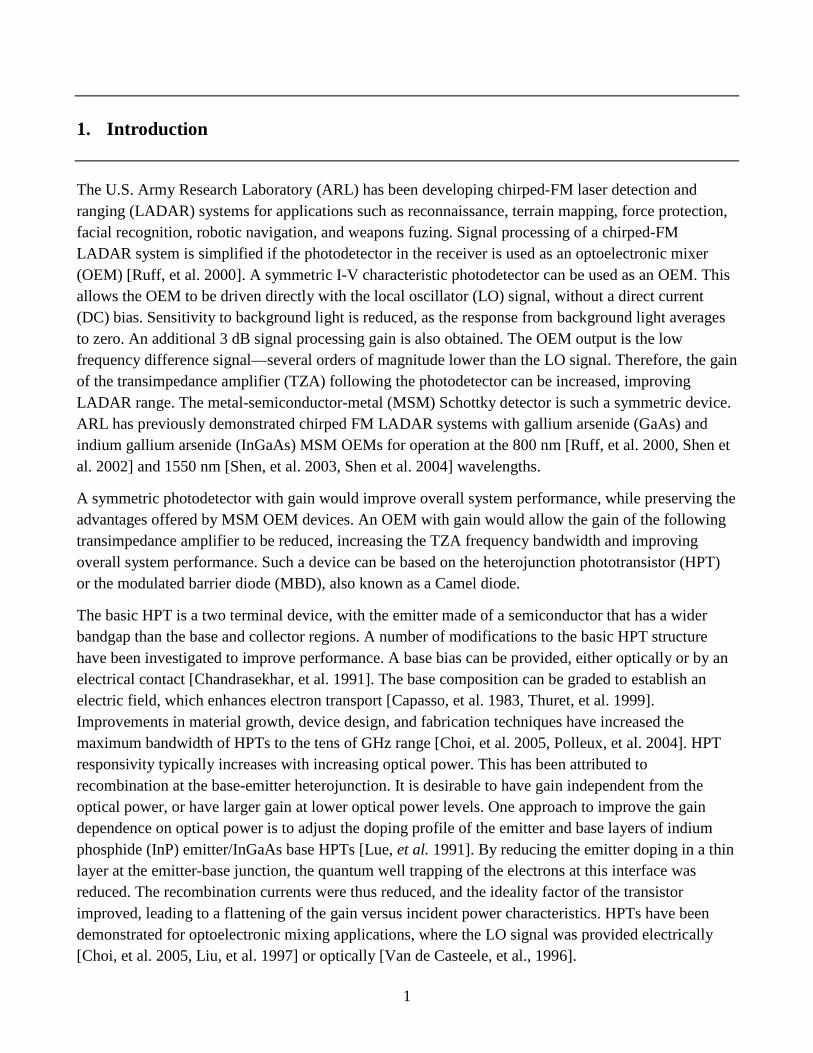
Figure 3 presents the calculated mixing efficiency of this device as a function of the LO voltage for the same optical power levels as figure 2. The device would reach theoretical equivalence to the present InGaAs MSMs at LO voltage levels of 11–12 dBm. An order of magnitude improvement would be achieved for 15–16 dBm (1.6–2 V peak), and two orders of magnitude improvement would be obtained at LO voltage levels of 23–25 dBm (4.5–5.6 V peak).
Figure 3. Predicted mixing responsivity vs. LO voltage for the device of figure 2.
Two structures were selected for growth following the initial one-dimensional simulation study. The layer structures of the two samples, referred to as Sample 1 and Sample 2 here on, are shown in figure 4. Detailed two-dimensional simulations were carried out to evaluate candidate device designs. Simulated I-V curves are presented later for the device design summarized in table 1.
300nm InAlAs bufferInP substrate
(S-doped, conductive)Sample 2
300nm InAlAs bufferInP substrate
(Fe-doped, semi-insulating)Sample 1
800nm p-InGaAs 2.5e16
390nm n-InAlAs 1e16
50nm n-InGaAs 1e19
50nm n-InAlAs 1e19
10nm n-InAlAs 5e18
10nm n-InAlAs 5e18
390nm n-InAlAs 1e1650nm n-InAlAs 1e19
300nm n-InGaAs 1e19
300nm p-InGaAs 2.5e16
500nm n-InAlAs 4e16
50nm n-InAlAs 4e16100nm n-InAlAs 5e17-1e18
300nm n-InAlAs 5e17-1e18
Figure 4. Vertical structure of the two samples selected for material growth and device fabrication.

5
Table 1. Simulated device parameters.
Size [µm] Inner mesa Outer mesa (bottom contact) Top contact width Top contact metal width Bottom contact width 2 Bottom contact metal width 4 Bond pads 80 x 80
Two-dimensional simulations of the devices were carried out using the Synopsys TCAD Sentaurus software suite. The Sentaurus Structure editor was used to construct the two-dimensional device, and the simulations were performed using Sentaurus Device.
Figure 5 shows the simulated current density profile in a two-dimensional cross section of a device on Sample 1. The insulation layers and metal stack are not shown for clarity. The active area diameter is 16 µm, and the top contact diameter is 12 µm. The bottom contact is 2 µm wide.
Figure 5. Current density distribution in a device with the Sample 1 layer structure.
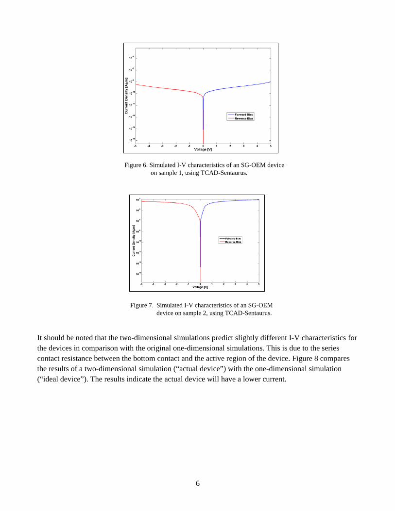
Figures 6 and 7 compare the forward and reverse bias currents for devices on Sample 1 and 2, with the dimensions listed in table 1. There is a slight asymmetry in the I-V curves due to the asymmetry of the two structures, more pronounced in Sample 2.
6
Figure 6. Simulated I-V characteristics of an SG-OEM device on sample 1, using TCAD-Sentaurus.
Figure 7. Simulated I-V characteristics of an SG-OEM device on sample 2, using TCAD-Sentaurus.
It should be noted that the two-dimensional simulations predict slightly different I-V characteristics for the devices in comparison with the original one-dimensional simulations. This is due to the series contact resistance between the bottom contact and the active region of the device. Figure 8 compares the results of a two-dimensional simulation (“actual device”) with the one-dimensional simulation (“ideal device”). The results indicate the actual device will have a lower current.

7
Figure 8. Comparison of I-V characteristics for an ‘ideal’ 1D SG-OEM device and an ‘actual’ 2D device showing the effect of the bottom contact placements on SG-OEM device performance
3. Material Growth and Device Fabrication
Mask design was done using Tanner L-Edit Pro 11. The die area is 1mm x 1mm. Each die has 32 devices of six basic designs, including square and circular devices. There are two types of circular devices, with ring contacts for top illumination and with circular contacts for bottom illumination through the substrate. The active area ranges from 18 µm to 30 µm for the circular devices, and from 10 µm to 16 µm for the square devices. Figure 9 shows a sample fabricated device, with a ring contact for top illumination.
Figure 9. Top-view photograph of a prototype symmetric gain optoelectronic mixer.

8
The two samples were grown at ARL using molecular beam epitaxy. The two mesa etches (top contact and device isolation) were done with an RIE-ICP etcher, using a chlorine/borontri-chloride (Cl2/BCl3) gas mixture. A 190 nm silicon nitride (Si3N4) anti-reflection coating was deposited for the top-illumination devices. This layer also served as an insulation layer for the bond pads. An ohmic contact metallization scheme of 50Å nickel (Ni) / 400Å germanium (Ge) / 1500Å gold (Au) was used.
4. Experimental Results
Current-voltage curves for two devices on sample 2 with r = 9 µm are shown in figure 10. ‘Dark’ refers to the dark current of the devices, while ‘light’ refers to the microscope light on the probe station being turned on during measurement. The voltage was applied to the top contact, and the bottom contact was grounded. There is a slight asymmetry in the I-V curves, due to the asymmetry in the structure of Sample 2 (figure 4).
Figure 10. I-V curves for top- (red) and back-side (blue) illumination devices with r = 9 µm.
Full characterization of the prototype devices is in progress at the time of the print. The full characterization will include DC responsivity, frequency response (AC responsivity), and mixing efficiency (mixing responsivity).

9
5. Conclusions
Symmetric gain optoelectronic mixers are promising for chirped-FM LADAR developed at ARL. Signal processing of a chirped-FM LADAR system is simplified if the photodetector in the receiver is used as an OEM. Adding gain to the OEM allows a reduction of the following transimpedance amplifier’s gain, increasing bandwidth, and improving the system’s noise performance. These symmetric gain OEM devices can lead to miniaturized LADAR-on-chip system. Such a system will have many military and civilian applications, such as range finding, terrain mapping, reconnaissance, and face recognition.
10
6. References
Ruff, W.; Bruno, J.; Kennerly, S.; Ritter, K.; Shen, P.; Stann, B.; Stead, M.; Sztankay, G.; Tobin, M. Self-mixing Detector Candidates for an FM/cw Ladar Architecture. Laser Radar Technology and Applications V, Proc. SPIE 2000, 4035, 152–62.
Shen, H.; Aliberti, K. Theoretical Snalysis of an Snisotropic Metal-semiconductor-metal Optoelectronic Mixer. J. Appl. Phys. 2002, 91 (6), 3880–90.
Shen, H.; Aliberti, K.; Stann, B.; Newman, P.; Mehandri, R.; Ren, F. Mixing Characteristics of InGaAs Metal-semiconductor-metal Photodetectors with Schottky Enhancement Layers. Appl. Phys. Lett. June 2003, 82 (22), 3814–6.
Shen, H.; Aliberti, K.; Stann, B.; Newman, P. G.; Mehandru, R.; Ren, F. Analysis of InGaAs Metal-Semiconductor-metal OE Mixers. Physics and Simulation of Optoelectronic Devices XII, Proc. SPIE 2004, 5349, 197–205.
Chandrasekhar, S.; Hoppe, M. K.; Dentai, A. G.; Joyner, C. H.; Qua, G. J. Demonstration of Enhanced Performance of an InP/InGaAs Heterojunction Phototransistor With a Base Terminal. IEEE Elec. Dev. Lett. October 1991, 12 (12), 550–552.
Capasso, F.; Tsang, W. T.; Bethea, C. G.; Hutchinson, A. L.; Levine, B. F. New Graded Band-gap Picosecond Phototransistor. Appl. Phys. Lett. January 1983, 42 (1), 93–95.
Thuret, J.; Gonzales, C.; Benchimol, J. L.; Riet, M.; Berdaguer, P. High-speed InP/InGaAs Heterojunction Phototransistor for Millimeter-wave Fibre Radio Communications. Proc. 11th Int. Conference on Indium Phosphide and Related Materials, 389–392 (1999)
Choi, C. S.; Seo, J. H.; Choi, W. Y.; Kamitsuna, H.; Ida, M.; Kurishima, K. 60-GHz Bidirectional Radio-on-Fiber Links Based on InP–InGaAs HPT Optoelectronic Mixers. IEEE Photon. Tech. Lett. December 2005, 17 (12), 2721–3.
Polleux, J. L.; Paszkiewicz, L.; Billabert, A. L.; Salset, J.; Rumelhard, C. Optimization of InP–InGaAs HPT Gain: Design of an Opto-Microwave Monolithic Amplifier. IEEE Trans. Microwave Theory Tech. March 2004, 52 (3), 871–81.
Leu, L. Y.; Gardner, J. T.; Forrest, S. R. A High-gain High-bandwidth In0.53Ga0.47As/InP Heterojunction Phototransistor for Optical Communications. J. Applied Physics January 1991, 69 (2), 1052.
Liu, C. P.; Seeds, A. J.; Wake, D. Two-terminal Ridge-coupled InP/InGaAs Heterojunction Phototransistor Optoelectronic Mixer. IEEE Microwave and Guided Wave Lett. March 1997, 7 (3), 72–74.

11
Van de Casteele, J.; Vilcot, J. P.; Gouy, J. P.; Mollot, F.; Decoster, D. Electro-optical Mixing in an Edge-coupled GaInAs/InP Heterojunction Phototransistor. Elec. Lett. May 1996, 32 (11), 1030–2.
Chen, C. Y.; Cho, A. Y.; Garbinski, P. A.; Bethea, C. G.; Levine, B. F. Modulated Barrier Photodiode: A New Majority-carrier Photodetector. Appl. Phys. Lett. August 1991, 39 (4), 340-2.
Chen, C. Y. Theory of a Modulated Barrier Photodiode. Appl. Phys. Lett. December 1981, 39 (12), 79–81.
Bethea, C. G.; Chen, C. Y.; Cho, A. Y.; Garbinski, P. A. Opto-electronic Picosecond Sampling System Utilizing a Modulated Barrier Photodiode. Appl. Phys. Lett. April 1982, 40 (7), 591–4.
Li, W. Q.; Bhattacharya, P. K. Integration of a Modulated Barrier Photodiode with a Doped-channel Quasi-MISFET. IEEE Elec. Dev. Lett. September 1989, 10 (9), 415–6.
Qasaimeh, O.; Zhou, W. D.; Bhattacharya, P.; Huffaker, D.; Deppe, D. G. Monolithically Integrated Low-Power Phototransceiver Incorporating InGaAs/GaAs Quantum-dot Microcavity LED and Modulated Barrier Photodiode. Electronics Lett. November 2000, 36 (23), 1955–7.

12
List of Symbols, Abbreviations, and Acronyms
ARL U.S. Army Research Laboratory
Au gold
Cl2/BCl3 chlorine/borontri-chloride
DC direct current
GaAs gallium arsenide
Ge germanium
HPT heterojunction phototransister
InGaAs indium gallium arsenide
InP indium phosphide
LADAR laser detection and ranging
LO local oscillator
MBD modulated barrier diode
MSM metal-semiconductor-metal
Ni nickel
OEM optoelectronic mixer
SG-OEM symmetric gain OEM
Si3N4 silicon nitride
TZA transimpedance ampelifier

13
NO. OF COPIES ORGANIZATION 1 ADMNSTR ELEC DEFNS TECHL INFO CTR ATTN DTIC OCP 8725 JOHN J KINGMAN RD STE 0944 FT BELVOIR VA 22060-6218 1 CD OFC OF THE SECY OF DEFNS ATTN ODDRE (R&AT) THE PENTAGON WASHINGTON DC 20301-3080 1 US ARMY RSRCH DEV AND ENGRG CMND ARMAMENT RSRCH DEV AND ENGRG CTR ARMAMENT ENGRG AND TECHNLGY CTR ATTN AMSRD AAR AEF T J MATTS BLDG 305 ABERDEEN PROVING GROUND MD 21005-5001 1 PM TIMS, PROFILER (MMS-P) AN/TMQ-52 ATTN B GRIFFIES BUILDING 563 FT MONMOUTH NJ 07703 1 US ARMY INFO SYS ENGRG CMND ATTN AMSEL IE TD A RIVERA FT HUACHUCA AZ 85613-5300
NO. OF COPIES ORGANIZATION 1 COMMANDER US ARMY RDECOM ATTN AMSRD AMR W C MCCORKLE 5400 FOWLER RD REDSTONE ARSENAL AL 35898-5000 1 US GOVERNMENT PRINT OFF DEPOSITORY RECEIVING SECTION ATTN MAIL STOP IDAD J TATE 732 NORTH CAPITOL ST NW WASHINGTON DC 20402 1 US ARMY RSRCH LAB ATTN RDRL CIM G T LANDFRIED BLDG 4600 ABERDEEN PROVING GROUND MD 21005-5066 7 US ARMY RSRCH LAB ATTN IMNE ALC HRR MAIL & RECORDS MGMT ATTN RDRL CIM L TECHL LIB ATTN RDRL CIM P TECHL PUB ATTN RDRL SEE M N BAMBHA (4 COPIES) ADELPHI MD 20783-1197 TOTAL: 15 (13 HCS, 1 CD, 1 ELEC)

14
INTENTIONALLY LEFT BLANK.


![Theoretical Analysis of InGaAs/InAlAs Single-Photon ......based APDs have high-electron mobility, leads to faster response times than that of InP-based APDs [16]. More-over, ionization](https://static.fdocuments.us/doc/165x107/60a9c8a12cb26c328b5f2fb4/theoretical-analysis-of-ingaasinalas-single-photon-based-apds-have-high-electron.jpg)