A Dynamic Voltage and Current Regulator Control Interface for the Linux Kernel.
Analysis of a Dynamic Voltage Regulator
A Low voltage compensation circuit based on an AC chopper
Wang Kai
Master of Science Thesis
Stockholm, Sweden 2009
XR-EE-EME 2009:010


I
Abstract
Dynamic Voltage Regulator(DVR) based on a PWM controlled AC chopper is proposed in the
present thesis. The DVR is suitable to settle the low-voltage problem at the terminals of the
distribution system, especially in rural power networks. The AC buck chopper is composed of
four self-turn-off devices and is controlled by the non-complementary method without
current detection. The operation principle of the switches is pulse width modulation (PWM),
and the duty cycle is adjusted according to the degree of voltage drop at the input line. The
compensation device is connected to the power supply line in series and starts up when the
line voltage drops. This device doesn’t need any energy storage component and it only acts on
the voltage difference. So the voltage rating can be kept low, which yields a low cost.
Additionaly it has a high reliability and wide compensation range. It is suitable for continuous
voltage regulation and long time operation. The accuracy and availability of this solution is
proved by the simulations.
Key words: power quality, dynamic voltage regulator, AC chopper, voltage compensation,
pulse width modulation
II
Index
ABSTRACT ................................................................................................................................................... I
INDEX ........................................................................................................................................................... II
FIGURES INDEX ...................................................................................................................................... IV
TABLES INDEX ........................................................................................................................................ VI
1. INTRODUCTION.............................................................................................................................. 1
1.1 DEVELOPMENT OF MODERN POWER ELECTRONICS............................................................................................... 1
1.1.1 Problem on Power Quality ............................................................................................................... 3
1.1.2 Classification of Power Quality Problems ........................................................................................ 4
1.1.3 The Influence of Power Quality Problem ......................................................................................... 5
1.2 VOLTAGE SAG AND SWELL ............................................................................................................................... 6
1.2.1 Definition ......................................................................................................................................... 6
1.2.2 Characterization and Effect ............................................................................................................. 6
1.2.3 Treatment ........................................................................................................................................ 9
1.3 THE AIMS ..................................................................................................................................................... 9
2. DYNAMIC VOLTAGE REGULATOR ......................................................................................... 10
2.1 CONSTRUCTION OF VOLTAGE REGULATOR [9] [10]
................................................................................................ 10
2.1.1 Main Circuit ................................................................................................................................... 10
2.1.2 Energy Storage Unit ...................................................................................................................... 11
2.1.3 Inverter .......................................................................................................................................... 12
2.1.4 Filter .............................................................................................................................................. 13
2.1.5 Connecting type [12]
........................................................................................................................ 14
2.2 PRINCIPLE OF WORK [17]
................................................................................................................................ 16
2.3 CONTROL STRATEGY OF VOLTAGE COMPENSATION [14]
........................................................................................ 21
2.3.1 Reactive power compensation ...................................................................................................... 22
2.3.2 In-phase compensation ................................................................................................................. 22
2.3.3 Best quality compensation ............................................................................................................ 22
2.3.4 Minimum power compensation .................................................................................................... 23
III
2.4 CONCLUSION .............................................................................................................................................. 23
3. CIRCUIT DESIGN .............................................................................................................................. 24
3.1 INTRODUCTION TO PSCAD ............................................................................................................................ 24
3.2 CIRCUIT ..................................................................................................................................................... 24
4. EXPERIMENT AND SIMULATION ................................................................................................. 30
4.1 GENERAL SIMULATION RESULT ........................................................................................................................ 30
4.2 ADJUSTMENT AND ADVANCED EXPERIMENT....................................................................................................... 33
4.3 CONCLUSION .............................................................................................................................................. 44
4.4 HARMONIC ANALYSIS .................................................................................................................................... 44
ACKNOWLEDGEMENT ............................................................................................................................ 46
REFERENCE .............................................................................................................................................. 47

IV
Figures index
Figure 1-1 Block diagram of a power electronic system ................................................................. 1
Figure 1-2 Regular power quality problem in Power system .......................................................... 4
Figure 1-4 Amplitude value of fundamental when unbalanced three-phases voltage sag happens
................................................................................................................................................. 7
Figure 1-3 a) Three-phase balance voltage sag, b)six types of three-phase unbalance voltage sags
................................................................................................................................................. 7
Figure 1-5 Amplitude value of fundamental when the induction-machine starts .......................... 8
Figure 2-1 Series and parallel connection DVR ............................................................................. 10
Figure 2-2 Series and parallel connection DVR ............................................................................. 11
Figure 2-3 Series DVR .................................................................................................................... 11
Figure 2-4 Three typical inverters ................................................................................................. 13
Figure 2-5 Three locations of filter ................................................................................................ 14
Figure 2-6 System block diagram .................................................................................................. 16
Figure 2-7 AC chopper circuit structure ........................................................................................ 17
Figure 2-8 Gate pulses for the IGBTs using non-complementary control ..................................... 17
Figure 2-9 Current path when P1, P2, P4 turn on and P3 turns off .............................................. 18
Figure 2-10 Current path when P1, P2, P4 turn on and P3 turns off ............................................ 18
Figure 2-11 Current path when P2, P4 turn on and P1, P3 turn off .............................................. 19
Figure 2-12 Current path when P2, P4 turn on and P1, P3 turn off .............................................. 19
Figure 2-13 Current path when P2, P3, P4 turn on and P1 turns off ............................................ 20
Figure 2-14 Current path when P3, P4 turn on and P1, P2 turn off .............................................. 20
Figure 2-15 Equivalent circuit of DVR ............................................................................................ 21
Figure 2-16 Compensation voltage vector .................................................................................... 21
Figure 2-17 Compensation voltage vector .................................................................................... 22
Figure 2-18 Compensation voltage vector .................................................................................... 22
Figure 2-19 Compensation voltage vector .................................................................................... 23
V
Figure 3-1 Whole view of Circuit ................................................................................................... 25
Figure 3-2 Block of power source .................................................................................................. 25
Figure 3-3 The impedance curve of Γ-type LPF ............................................................................. 26
Figure 3-4 Filter circuit .................................................................................................................. 28
Figure 3-5 Inverter unit ................................................................................................................. 28
Figure 3-6 Actuating signal control................................................................................................ 29
Figure 4-1 RMS value of voltage waveform .................................................................................. 30
Figure 4-2 Zoom-in graph of system voltage usys ......................................................................... 31
Figure 4-3 Compensation output voltage waveform .................................................................... 31
Figure 4-4 Load voltage waveform ................................................................................................ 32
Figure 4-5 RMS value of voltage waveform .................................................................................. 32
Figure 4-6 Measuring point ........................................................................................................... 33
Figure 4-7 comparison of voltage on different winding in normal size and in expanding view ... 34
Figure 4-8 comparison of voltage on S2 and primary winding in normal size and in expanding
view ....................................................................................................................................... 34
Figure 4-9 comparison of voltage on S1 and primary winding in normal size and in expanding
view ....................................................................................................................................... 35
Figure 4-10 comparison of voltage on S4 and primary winding in normal size and in expanding
view ....................................................................................................................................... 35
Figure 4-11 comparison of voltage on S3 and primary winding in normal size and in expanding
view ....................................................................................................................................... 36
Figure 4-12 comparison of voltage on resistance and primary winding ....................................... 36
Figure 4-13 comparison of input voltage and voltage on primary winding in normal size and in
expanding view ...................................................................................................................... 37
Figure 4-14 comparison of the peak value of input voltage and voltage in primary winding ...... 37
Figure 4-15 ..................................................................................................................................... 38
Figure 4-16 ..................................................................................................................................... 38
Figure 4-17 comparison of input voltage Vac and output voltage in normal size and expanding
view ....................................................................................................................................... 39

VI
Figure 4-18 comparison of input voltage Vac and output voltage in normal size and expanding
view ....................................................................................................................................... 40
Figure 4-19 Waveform when S3 or S1 turns off ............................................................................ 40
Figure 4-20 Source voltage and its expanding graph .................................................................... 41
Figure 4-21 Input voltage and its expanding graph ....................................................................... 41
Figure 4-22 Compensation voltage and its expanding graph ........................................................ 42
Figure 4-23 Load voltage and its expanding graph ....................................................................... 42
Figure 4-24 General view and zoom-in view of waveform when S1 turns off .............................. 43
Figure 4-25 General view and zoom-in view of waveform when S2 turns off .............................. 43
Figure 4-26 General view and zoom-in view of waveform when S3 turns off .............................. 43
Figure 4-27 General view and zoom-in view of waveform when S4 turns off .............................. 44
Tables index
Table 1-1 Power Electronics Applications [1]
.................................................................................... 2
Table 1-2 Character and classification of electromagnetic phenomenon in IEEE standard [2]
........ 4
Table 1-3 Definition of Different kinds of power quality problems ................................................ 5
Table 4-1 Parameters .................................................................................................................... 33
Table 4-2 Parameters .................................................................................................................... 39
Table 4-3 Parameters .................................................................................................................... 39
Table 4-4 Parameters .................................................................................................................... 41
1. Introduction
1
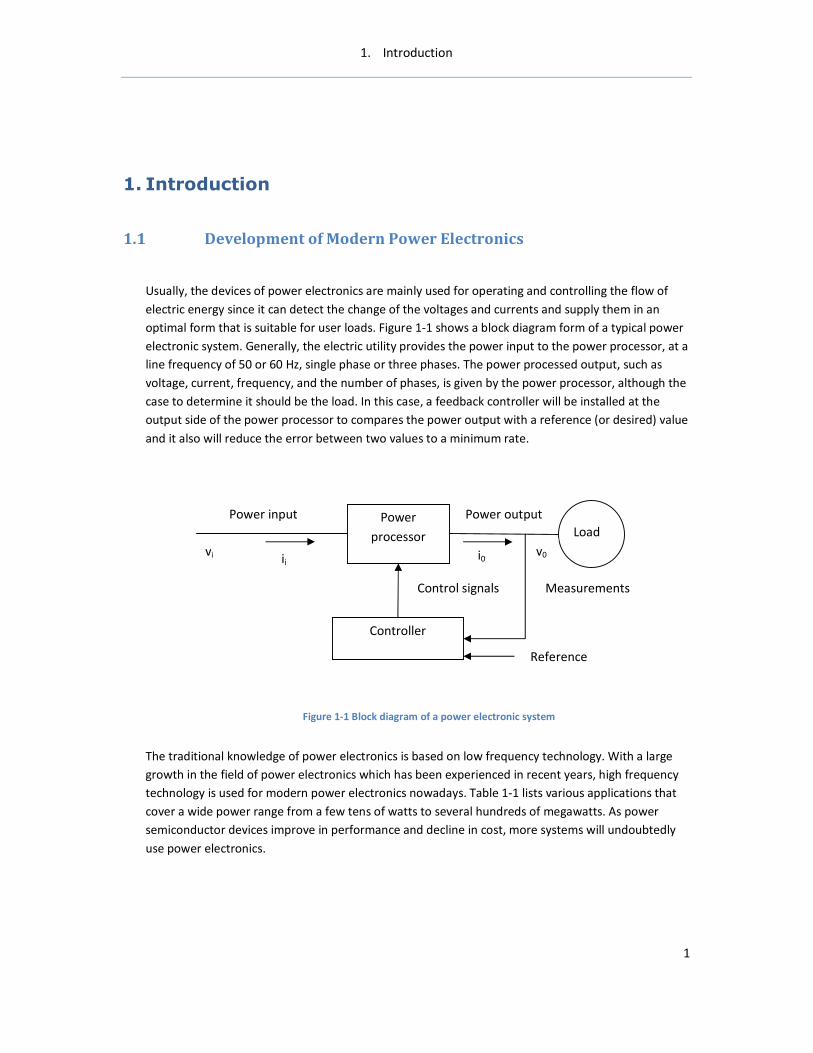
1. Introduction
1.1 Development of Modern Power Electronics
Usually, the devices of power electronics are mainly used for operating and controlling the flow of
electric energy since it can detect the change of the voltages and currents and supply them in an
optimal form that is suitable for user loads. Figure 1-1 shows a block diagram form of a typical power
electronic system. Generally, the electric utility provides the power input to the power processor, at a
line frequency of 50 or 60 Hz, single phase or three phases. The power processed output, such as
voltage, current, frequency, and the number of phases, is given by the power processor, although the
case to determine it should be the load. In this case, a feedback controller will be installed at the
output side of the power processor to compares the power output with a reference (or desired) value
and it also will reduce the error between two values to a minimum rate.
The traditional knowledge of power electronics is based on low frequency technology. With a large
growth in the field of power electronics which has been experienced in recent years, high frequency
technology is used for modern power electronics nowadays. Table 1-1 lists various applications that
cover a wide power range from a few tens of watts to several hundreds of megawatts. As power
semiconductor devices improve in performance and decline in cost, more systems will undoubtedly
use power electronics.
Load Power
processor
Controller
Power input Power output
Measurements
Reference
Control signals
vi ii v0 i0
Figure 1-1 Block diagram of a power electronic system

1. Introduction
2
(a) Residential (d) Transportation
Refrigeration and freezers
Space heating
Air conditioning
Cooking
Lighting
Electronics (personal computers, etc.)
Traction control of electric vehicles
Battery chargers for electric vehicles
Electric locomotives
Street cars, trolley buses
Subways
Automotive electronics including engine control
(b) Commercial (e) Utility systems
Heating, ventilating, and air conditioning
Central refrigeration
Lighting
Computers and office equipment
Uninterruptible power supplies (UPSs)
Elevators
High-voltage dc transmission (HVDC)
Static var compensation (SVC)
Supplemental energy sources, fuel cells
Energy storage systems
Induced-draft fans and boiler feed water pumps
Dynamic voltage regulator (DVR)
(c) Industrial (f) Aerospace
Pumps
Compressors
Blowers and fans
Machine tools (robots)
Arc furnaces, induction furnaces
Lighting
Industrial lasers
Induction heating
Welding
Space shuttle power supply systems
Satellite power systems
Aircraft power systems
(g) Telecommunications
Battery chargers
Power supplies (dc and UPS)
Table 1-1 Power Electronics Applications [1]
1. Introduction
3
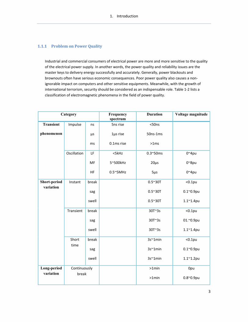
1.1.1 Problem on Power Quality
Industrial and commercial consumers of electrical power are more and more sensitive to the quality
of the electrical power supply. In another words, the power quality and reliability issues are the
master keys to delivery energy successfully and accurately. Generally, power blackouts and
brownouts often have serious economic consequences. Poor power quality also causes a non-
ignorable impact on computers and other sensitive equipments. Meanwhile, with the growth of
international terrorism, security should be considered as an indispensable role. Table 1-2 lists a
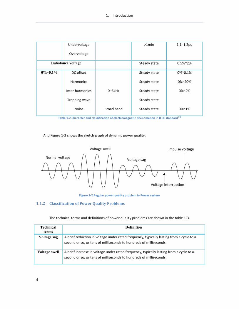
classification of electromagnetic phenomena in the field of power quality.
Category Frequency
spectrum
Duration Voltage magnitude
Transient
phenomenon
Impulse ns
μs
ms
5ns rise
1μs rise
0.1ms rise
<50ns
50ns-1ms
>1ms
Oscillation LF
MF
HF
<5kHz
5~500kHz
0.5~5MHz
0.3~50ms
20μs
5μs
0~4pu
0~8pu
0~4pu
Short-period
variation
Instant break
sag
swell
0.5~30T
0.5~30T
0.5~30T
<0.1pu
0.1~0.9pu
1.1~1.4pu
Transient break
sag
swell
30T~3s
30T~3s
30T~3s
<0.1pu
01.~0.9pu
1.1~1.4pu
Short
time
break
sag
swell
3s~1min
3s~1min
3s~1min
<0.1pu
0.1~0.9pu
1.1~1.2pu
Long-period
variation
Continuously
break
>1min
>1min
0pu
0.8~0.9pu
1. Introduction
4
Undervoltage
Overvoltage
>1min 1.1~1.2pu
Imbalance voltage Steady state 0.5%~2%
0%~0.1% DC offset
Harmonics
Inter-harmonics
Trapping wave
Noise
0~6kHz
Broad band
Steady state
Steady state
Steady state
Steady state
Steady state
0%~0.1%
0%~20%
0%~2%
0%~1%
Table 1-2 Character and classification of electromagnetic phenomenon in IEEE standard [2]
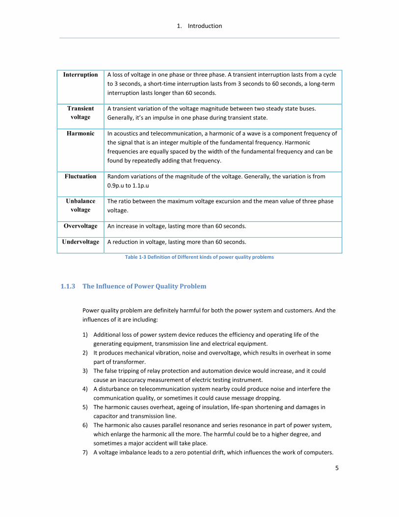
And Figure 1-2 shows the sketch graph of dynamic power quality.
Figure 1-2 Regular power quality problem in Power system
1.1.2 Classification of Power Quality Problems
The technical terms and definitions of power quality problems are shown in the table 1-3.
Technical
terms
Definition
Voltage sag A brief reduction in voltage under rated frequency, typically lasting from a cycle to a
second or so, or tens of milliseconds to hundreds of milliseconds.
Voltage swell A brief increase in voltage under rated frequency, typically lasting from a cycle to a
second or so, or tens of milliseconds to hundreds of milliseconds.
Normal voltage
Voltage swell
Voltage sag
Voltage interruption
Impulse voltage
1. Introduction
5
Interruption A loss of voltage in one phase or three phase. A transient interruption lasts from a cycle
to 3 seconds, a short-time interruption lasts from 3 seconds to 60 seconds, a long-term
interruption lasts longer than 60 seconds.
Transient
voltage
A transient variation of the voltage magnitude between two steady state buses.
Generally, it’s an impulse in one phase during transient state.
Harmonic In acoustics and telecommunication, a harmonic of a wave is a component frequency of
the signal that is an integer multiple of the fundamental frequency. Harmonic
frequencies are equally spaced by the width of the fundamental frequency and can be
found by repeatedly adding that frequency.
Fluctuation Random variations of the magnitude of the voltage. Generally, the variation is from
0.9p.u to 1.1p.u
Unbalance
voltage
The ratio between the maximum voltage excursion and the mean value of three phase
voltage.
Overvoltage An increase in voltage, lasting more than 60 seconds.
Undervoltage A reduction in voltage, lasting more than 60 seconds.
Table 1-3 Definition of Different kinds of power quality problems
1.1.3 The Influence of Power Quality Problem
Power quality problem are definitely harmful for both the power system and customers. And the
influences of it are including:
1) Additional loss of power system device reduces the efficiency and operating life of the
generating equipment, transmission line and electrical equipment.
2) It produces mechanical vibration, noise and overvoltage, which results in overheat in some
part of transformer.
3) The false tripping of relay protection and automation device would increase, and it could
cause an inaccuracy measurement of electric testing instrument.
4) A disturbance on telecommunication system nearby could produce noise and interfere the
communication quality, or sometimes it could cause message dropping.
5) The harmonic causes overheat, ageing of insulation, life-span shortening and damages in
capacitor and transmission line.
6) The harmonic also causes parallel resonance and series resonance in part of power system,
which enlarge the harmonic all the more. The harmful could be to a higher degree, and
sometimes a major accident will take place.
7) A voltage imbalance leads to a zero potential drift, which influences the work of computers.
1. Introduction
6
1.2 Voltage Sag and Swell
A rough statistics suggests that about 92% of the interruptions in industrial installations are voltage
sag related.[3]
And in most cases, the problem is caused by remote faults or changes in the loading
condition.
1.2.1 Definition
The voltage sag as defined by IEEE standard 1159-1995, IEEE Recommended Practice for
Monitoring Electric Power Quality, is: “a brief reduction in voltage, typically lasting from a cycle to
a second or so, or tens of milliseconds to hundreds of milliseconds.” To the contrary, voltage
swell is a brief increases in voltage over the same time range. But a low or high voltage last in
longer periods is referred to as “undervoltage” or “overvoltage”.
The voltage sag/swell lasts just as little as a few cycles, but it can also affect some certain
sensitive loads, such as adjustable speed drives (ASD) and programmable logic controllers (PLC).
1.2.2 Characterization and Effect
Voltage sag
The causes for voltage sags are abrupt increases in loads, such as disturbances, induction-
machine starting, electric heaters turning on, or an unplanned increase in source impedance
caused by a loose connection, etc. On the contrary, voltage swells are almost always caused by an
abrupt reduction in loads, such as a poor or damaged voltage regulator. Besides all, they can also
be caused by a damaged or loose neutral connection. [4]
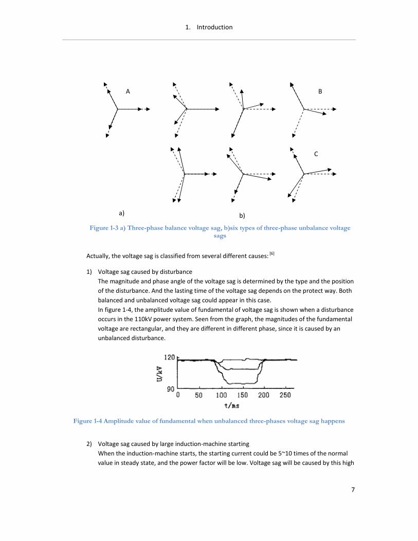
Based on symmetrical components, the voltage sag type indicates which phases are involved in
the event. Figure 1-3 gives a basic type of balanced voltage sag and six types of unbalanced
voltage sags.
Balanced voltage sag (type A) is due to an equal drop in the values of voltage in three-phases.
Unbalanced voltage sag (types B and C) is due to a drop between two phases or a drop in one
phase.[5]
1. Introduction
7
Actually, the voltage sag is classified from several different causes: [6]
1) Voltage sag caused by disturbance
The magnitude and phase angle of the voltage sag is determined by the type and the position
of the disturbance. And the lasting time of the voltage sag depends on the protect way. Both
balanced and unbalanced voltage sag could appear in this case.
In figure 1-4, the amplitude value of fundamental of voltage sag is shown when a disturbance
occurs in the 110kV power system. Seen from the graph, the magnitudes of the fundamental
voltage are rectangular, and they are different in different phase, since it is caused by an
unbalanced disturbance.
Figure 1-4 Amplitude value of fundamental when unbalanced three-phases voltage sag happens
2) Voltage sag caused by large induction-machine starting
When the induction-machine starts, the starting current could be 5~10 times of the normal
value in steady state, and the power factor will be low. Voltage sag will be caused by this high
Figure 1-3 a) Three-phase balance voltage sag, b)six types of three-phase unbalance voltage sags
a) b)
A B
C
1. Introduction
8
starting current, and the magnitude of it depends on the characteristic of the induction-
machine and the short-current capacity of the system.
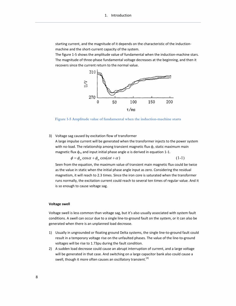
The figure 1-5 shows the amplitude value of fundamental when the induction-machine stars.
The magnitude of three-phase fundamental voltage decreases at the beginning, and then it
recovers since the current return to the normal value.
Figure 1-5 Amplitude value of fundamental when the induction-machine starts
3) Voltage sag caused by excitation flow of transformer
A large impulse current will be generated when the transformer injects to the power system
with no-load. The relationship among transient magnetic flux ϕ, static maximum main
magnetic flux ϕm and input initial phase angle α is derived in equation 1-1.
cos cos( ) (1-1)m m tφ φ α φ ω α= + +
Seen from the equation, the maximum value of transient main magnetic flux could be twice
as the value in static when the initial phase angle input as zero. Considering the residual
magnetism, it will reach to 2.3 times. Since the iron core is saturated when the transformer
runs normally, the excitation current could reach to several ten times of regular value. And it
is so enough to cause voltage sag.
Voltage swell
Voltage swell is less common than voltage sag, but it’s also usually associated with system fault
conditions. A swell can occur due to a single line-to-ground fault on the system, or it can also be
generated when there is an unplanned load decrease.
1) Usually in ungrounded or floating ground Delta systems, the single line-to-ground fault could
result in a temporary voltage rise on the unfaulted phases. The value of the line-to-ground
voltages will be rise to 1.73pu during the fault condition.
2) A sudden load decrease could cause an abrupt interruption of current, and a large voltage
will be generated in that case. And switching on a large capacitor bank also could cause a
swell, though it more often causes an oscillatory transient.[4]
1. Introduction
9
1.2.3 Treatment
Several ways to correct the voltage sag/swell are commonly used nowadays. [7]
1) Uninterruptable Power Supply (UPS)
A continuous power supply will be used during the period of voltage sag/swell in high
efficient as 92%~97%. An expensive expense and restricted capacity is the disadvantage of
UPS.
2) Constant Voltage Transformer (CVT)
It’s generally used under 20kVA power system. A balanced voltage will be supplied even the
voltage drops to the 70% of normal value. And its efficient is between 70%~75%.
3) Static Transfer Switch (STS)
It’s set in a dual-power system. When one of the power supplies has problem, the STS will
switch to another one as the power supply for the load.
4) Transformer Tap-Change (TC)
It can reduce the effect of voltage sag/swell during a certain extent, which is determined by
the adjusting range of the tap changer.
5) Motor-Generator (MG)
The inertia of the motor could be used to keep the normal voltage when the voltage
sag/swell happens.
6) Dynamic Voltage Regulator (DVR)
It’s the cheapest device according to the other ones. It has a high efficient, since the DVR
only works when the voltage sag/swell happens.
1.3 The aims
Due to the excellent dynamic performance of the Dynamic Voltage Regulator it is the most efficiency
solution dealing with the dynamic voltage problem. Additionally, the large capacity of the DVR makes
it as an economic method also.
The analysis of DVR will be performance in several divisions during the following work:
1) Construction, operation principle of DVR
An overall presentation of the whole system and some detailed description of each component
will be given in the second chapter.
2) Corresponding circuit design of DVR
To use PSCAD to organize an AC buck chopper circuit that is corresponding to the DVR.
3) Simulation
Some simulations and comparisons will be given in the forth chapter.
2. Dynamic Voltage Regulator
10
2. Dynamic Voltage Regulator
2.1 Construction of Voltage regulator [9] [10]
The Dynamic Voltage Regulator consists of several parts. Besides of the structure, the control strategy
is also an important thing to consider. In this section, the construction a DVR and some regular control
strategies for it will be introduced.
2.1.1 Main Circuit
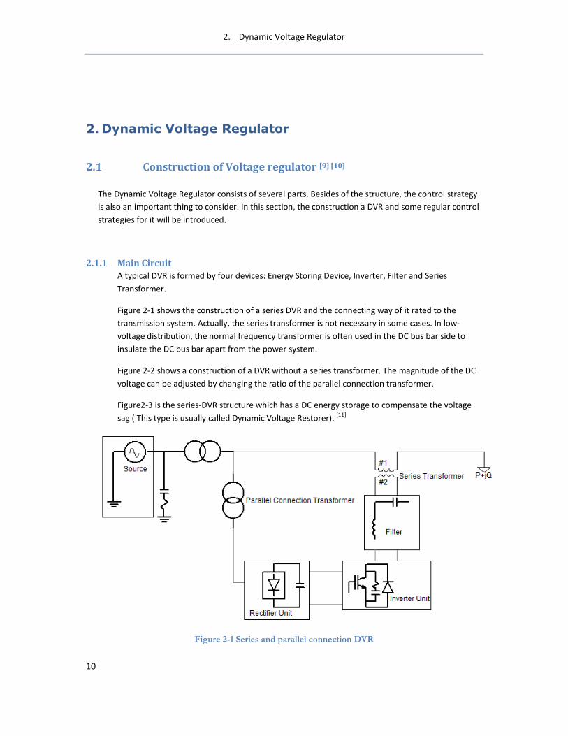
A typical DVR is formed by four devices: Energy Storing Device, Inverter, Filter and Series
Transformer.
Figure 2-1 shows the construction of a series DVR and the connecting way of it rated to the
transmission system. Actually, the series transformer is not necessary in some cases. In low-
voltage distribution, the normal frequency transformer is often used in the DC bus bar side to
insulate the DC bus bar apart from the power system.
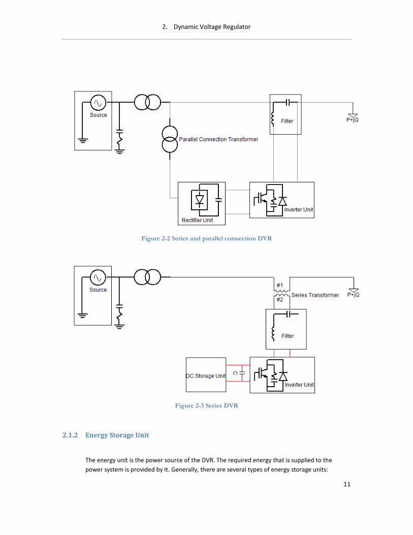
Figure 2-2 shows a construction of a DVR without a series transformer. The magnitude of the DC
voltage can be adjusted by changing the ratio of the parallel connection transformer.
Figure2-3 is the series-DVR structure which has a DC energy storage to compensate the voltage
sag ( This type is usually called Dynamic Voltage Restorer). [11]
Figure 2-1 Series and parallel connection DVR
2. Dynamic Voltage Regulator
11
Figure 2-2 Series and parallel connection DVR
Figure 2-3 Series DVR
2.1.2 Energy Storage Unit
The energy unit is the power source of the DVR. The required energy that is supplied to the
power system is provided by it. Generally, there are several types of energy storage units:

2. Dynamic Voltage Regulator
12
1) Accumulator cell
An accumulator cell not only provides reactive power adjusting, but also provides active
power supply. And it can continue to supply the device when the power system is blackout
for a short time, performing as an UPS. But an accumulator cell could only provide a short
time compensation because of its capability limit. Furthermore it’s expensive and it needs
maintenance, which leading to an increase of the cost of DVR.
2) Energy supply by power system through Non-controlled rectifier
A rectifier energy supply system could work continuous in a long period. But the main defect
is that the energy only has an one-way flow from system to the capacitor. So when voltage
swell occurs, the DC voltage will increase sharply.
3) Energy supply by power system through controlled rectifier
The main improve is to solve the one-way flow problem. But a more complicated system
needs more complex control strategy and increases the cost of DVR.
4) Other types
Superconductivity energy supply has high efficiency of energy transformation, and the
response time is very short. Moreover, it is easy maintenance and it has no power pollution
to the system. But such technique is still immature now, and the research on it will be
continuing.
2.1.3 Inverter
The inverter is used to produce a compensation voltage into the power transmission line.
Generally, it has several kinds of structure, such as semi-bridge, full-bridge and push-pull. In DVR
design, the full-bridge inverter is the mostly used. It could compensate the zero sequence voltage,
and it is easy to control. However, it has the bridge-arm shoot-through problem. Therefore, when
such kind of structure is used, a reliable bridge-arm protection must be supplied.
The main advantage of the push-pull inverter is that, at any moment there is no more than one
switching device operating. This means that the bridge-arm shoot-through problem eliminated.
However, the voltage rating of the switch is twice of the capacitor voltage. So it is more suitable
for a high power converter.
Figure 2-4 shows examples of typical half bridge, full bridge and push-pull inverters for DVRs,

2. Dynamic Voltage Regulator
13
Figure 2-4 Three typical inverters
2.1.4 Filter
The inverter also produces harmonics into the circuit. Therefore, a filter is installed to eliminate
the harmonics. And the inverter in different locations could give different influence on the DVR.
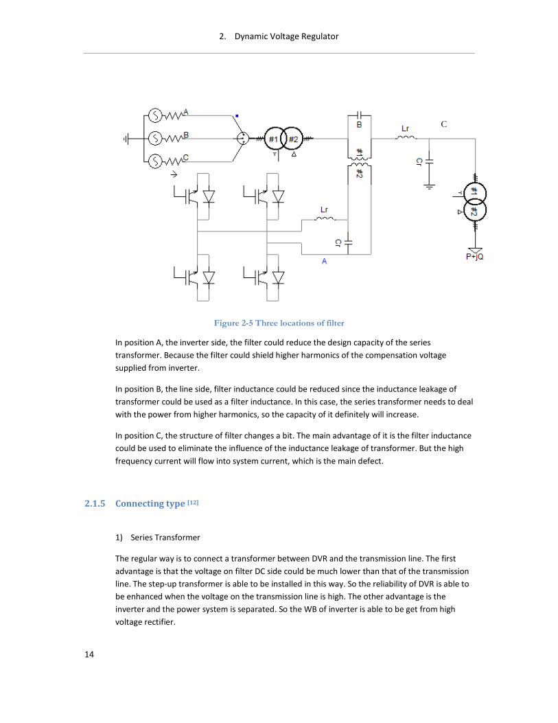
Figure 2-5 shows three different location of inverter in a DVR.
2. Dynamic Voltage Regulator
14
Figure 2-5 Three locations of filter
In position A, the inverter side, the filter could reduce the design capacity of the series
transformer. Because the filter could shield higher harmonics of the compensation voltage
supplied from inverter.
In position B, the line side, filter inductance could be reduced since the inductance leakage of
transformer could be used as a filter inductance. In this case, the series transformer needs to deal
with the power from higher harmonics, so the capacity of it definitely will increase.
In position C, the structure of filter changes a bit. The main advantage of it is the filter inductance
could be used to eliminate the influence of the inductance leakage of transformer. But the high
frequency current will flow into system current, which is the main defect.
2.1.5 Connecting type [12]
1) Series Transformer
The regular way is to connect a transformer between DVR and the transmission line. The first
advantage is that the voltage on filter DC side could be much lower than that of the transmission
line. The step-up transformer is able to be installed in this way. So the reliability of DVR is able to
be enhanced when the voltage on the transmission line is high. The other advantage is the
inverter and the power system is separated. So the WB of inverter is able to be get from high
voltage rectifier.
C
2. Dynamic Voltage Regulator
15
However, since the transformer is a non-linear device, it will introduce some disadvantages
indeed.
Firstly, high-frequency harmonics from the inverter causes difficulties in the transformer design.
In this case, a higher capacity transformer must be used. Sometimes a filter at the output could
be installed to solve the problem, but it will increase the cost of system significantly. Furthermore,
especially in high voltage and high capacity systems, the design of such a filter is very difficult.
Secondly, the influence between series transformer and L-C filter certainly will bring an additional
phase shift and voltage sag. Using a closed-loop voltage control is one way to solve the problem,
but it also will increase the complexity of the control.
Thirdly, the introduction of a transformer obviously increases the cost of the system.
In conclusion, a usage of series transformer needs to consider all kinds of factors and the
particulars of the power system in practical. Especially when it comes to a high-voltage power
system, the series transformer is the preferable choice after considering the DVR structure, the
DC-link voltage, and the cost of the devices.
2) Capacitance[13]
In low-voltage power systems, a transformerless structure usually applies. Figure 2-2 shows a
structure of this kind. When there is no series transformer, the DC side of the inverter must be
separated from the power system. A power transformer is often installed to achieve such
separation.
2. Dynamic Voltage Regulator
16
2.2 Principle of Work [17]
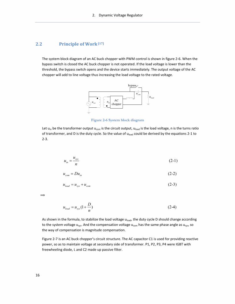
The system block diagram of an AC buck chopper with PWM control is shown in figure 2-6. When the
bypass switch is closed the AC buck chopper is not operated. If the load voltage is lower than the
threshold, the bypass switch opens and the device starts immediately. The output voltage of the AC
chopper will add to line voltage thus increasing the load voltage to the rated voltage.
AC
chopperinu
sysu
comu
loadu
bypass
Figure 2-6 System block diagram
Let uin be the transformer output ucom is the circuit output, uload is the load voltage, n is the turns ratio
of transformer, and D is the duty cycle. So the value of uload could be derived by the equations 2-1 to
2-3.
(2-1)sys
in
uu
n=
(2-2)com inu Du=
(2-3)load sys comu u u= +
⟹
(1 ) (2-4)load sys
Du u
n= +
As shown in the formula, to stabilize the load voltage uload, the duty cycle D should change according
to the system voltage usys. And the compensation voltage ucom has the same phase angle as usys, so
the way of compensation is magnitude compensation.
Figure 2-7 is an AC buck chopper’s circuit structure. The AC capacitor C1 is used for providing reactive
power, so as to maintain voltage at secondary side of transformer. P1, P2, P3, P4 were IGBT with
freewheeling diode, L and C2 made up passive filter.

2. Dynamic Voltage Regulator
17
Figure 2-7 AC chopper circuit structure
This circuit operates under the strategy of non-complementary control without current detection.
During the positive half cycle, P1 and P3 are closed in turns while P2 and P4 are kept closed. On the
contrary, in negative half cycle P2 and P4 are closed in turns while P1 and P3 are kept closed. [19]
Figure 2-8 Gate pulses for the IGBTs using non-complementary control
Through closed-loop feedback, the duty cycle changes according to the degree of voltage drop at
system network. The difference between uload and 220V is the necessary compensation voltage. D is
defined as:
220 (2-5)load
in
uD
u
−=
P1~P4 are controlled with PWM according to D. Then the output voltage of this circuit is adjusted
smoothly.
The topological modes are classified into active mode, dead time, and freewheeling modes. The
inductor current flows through the voltage source during the active mode. The current direction is
shown in figure 2-9 and 2-10.

2. Dynamic Voltage Regulator
18
Figure 2-9 Current path when P1, P2, P4 turn on and P3 turns off
P1 P2
P4
P3T1
D1D2
D3
D4
L
C
R
Figure 2-10 Current path when P1, P2, P4 turn on and P3 turns off

2. Dynamic Voltage Regulator
19
Then two modulated switches are turned off, the circuit comes in to dead-time mode. The current
path is shown in figure 2-11 and 2-12.
P1 P2
P4
P3T1
D1D2
D3
D4
L
C
R
Figure 2-11 Current path when P2, P4 turn on and P1, P3 turn off
Figure 2-12 Current path when P2, P4 turn on and P1, P3 turn off
2. Dynamic Voltage Regulator
20
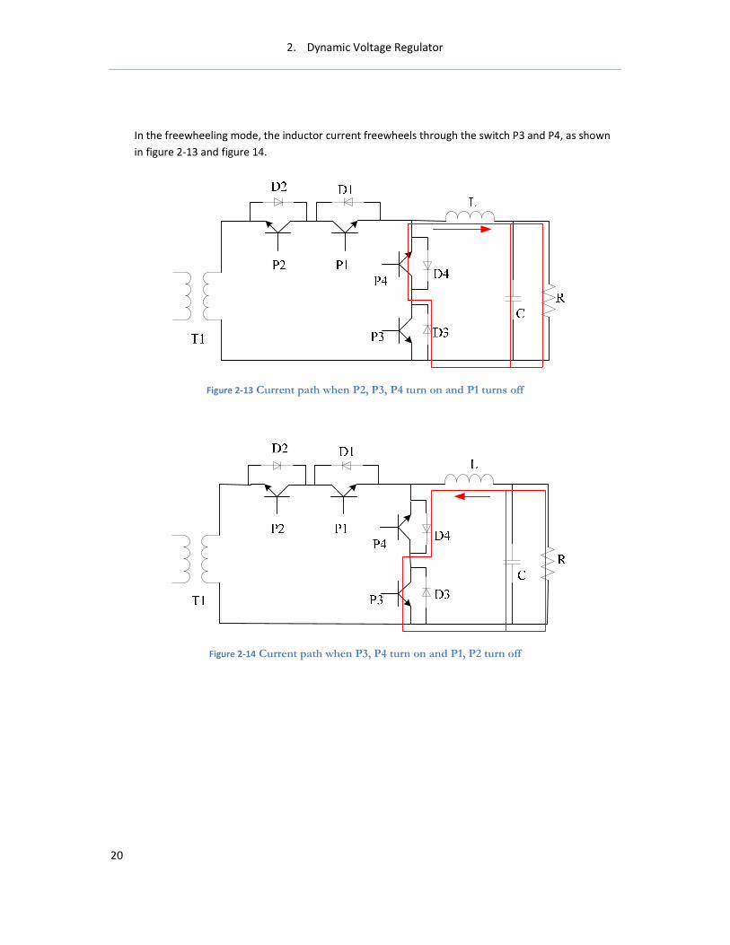
In the freewheeling mode, the inductor current freewheels through the switch P3 and P4, as shown
in figure 2-13 and figure 14.
Figure 2-13 Current path when P2, P3, P4 turn on and P1 turns off
Figure 2-14 Current path when P3, P4 turn on and P1, P2 turn off
2. Dynamic Voltage Regulator
21
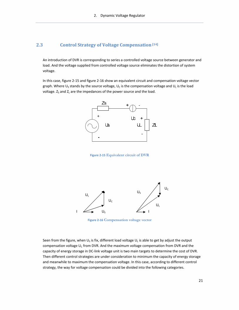
2.3 Control Strategy of Voltage Compensation [14]
An introduction of DVR is corresponding to series a controlled voltage source between generator and
load. And the voltage supplied from controlled voltage source eliminates the distortion of system
voltage.
In this case, figure 2-15 and figure 2-16 show an equivalent circuit and compensation voltage vector
graph. Where US stands by the source voltage, UC is the compensation voltage and UL is the load
voltage. ZS and ZL are the impedances of the power source and the load.
Figure 2-15 Equivalent circuit of DVR
Seen from the figure, when US is fix, different load voltage UL is able to get by adjust the output
compensation voltage UC from DVR. And the maximum voltage compensation from DVR and the
capacity of energy storage in DC-link voltage unit is two main targets to determine the cost of DVR.
Then different control strategies are under consideration to minimum the capacity of energy storage
and meanwhile to maximum the compensation voltage. In this case, according to different control
strategy, the way for voltage compensation could be divided into the following categories.
UC
UL
US I
US
UL
UC
I
Figure 2-16 Compensation voltage vector

2. Dynamic Voltage Regulator
22
2.3.1 Reactive power compensation
In this case the DVR could not provide active power compensation to a DC-link voltage unit, but it
could compensate reactive power. So the compensation voltage UC keeps vertical to load current
IL. In figure 2-17, US and UL are the voltage in system side and voltage in load side when the sag
occurs, UC is the compensation voltage, U is the system voltage in nominal condition, ϕ is the
power coefficient angle of the load, α is the phase trip angle when sag occurs, and θ is the power
coefficient angle of the compensation output. And in this case, θ=90°.
2.3.2 In-phase compensation
The compensation voltage UC has the same phase angle as the system voltage US. In figure 2-18,
ϕ=θ, so the magnitude of compensation voltage output from DVR is minimum. And both active
power and reactive power are compensated in this way.
2.3.3 Best quality compensation
US
UL
U
UC
IL
θ
α
ϕ
US
UL U
UC
IL
θ α
ϕ
Figure 2-17 Compensation voltage vector
Figure 2-18 Compensation voltage vector

2. Dynamic Voltage Regulator
23
The magnitude and phase angle of load voltage are compensated to the same as before the sag
occurs. It is suitable for the sensitive load, which has a strict quality demand in voltage magnitude
and phase angle. And figure 2-19 shows the vector graph. Also both active power and reactive
power are compensated in this way.
2.3.4 Minimum power compensation
Two ways mentioned above, which are able to compensate both active power and reactive
power, have demanding in active power supply of DC-link voltage unit. And the output energy of
both of them are not able to control. So when the voltage swell occurs, the energy might be
backward. And it will cause a boost arise of DC capacitor voltage.
As a result, the way to minimum power compensation is brought forward. And the active power
output is cosC LP U I θ= × × . Since the DVR is series connection between generator and load,
it has the same current as the load current IL. So in order to reduce the active power output P, the
magnitude of compensation voltage UC should reduce or the power coefficient angle θ should
increase. And the way to realize minimum power compensation is to force the output voltage
vector being vertical to the load current by change the phase angle between output voltage and
load current. At this moment, the output active power from DVR is minimised. So in another
saying, the way of reactive power compensation is a particular case of minimum power
compensation.
2.4 Conclusion
1) Description on the main structure of DVR, and comparison between the series transformer
connecting way and non series transformer connecting way are given in this section. And the
position where the filter unit is switched in is discussed also.
2) The principle and the course of the work of DVR is explained. The AC buck chopper’s circuit
structure is described and analysis in detail.
3) Four different voltage compensation strategies are explained: reactive power compensation, in-
phase compensation, best quality compensation and minimum power compensation.
Figure 2-19 Compensation voltage vector
US
UL
U
UC
IL
θ
α
ϕ

3. Circuit Design
24
3. Circuit Design
The circuit of DVR is formed in PSCAD software. And the simulation should be given in specified
environment. Especially, the influence of the modules should be consider, and the experiment will be
given based on it.
3.1 Introduction to PSCAD
PSCAD(Power System Computer Aided Design) is a popular software for power system design and
simulation. It was developed by Dr. Dennis Woodford since year 1976. It is the pre-processing
program of EMTDC(Electro Magnetic Transient in DC System). The customers could form electrical
circuit, input the parameter of each component and compile by the FORTRAN compiler. The result is
able to display in PLOT windows along with the working procedure. Besides all, PSCAD has an
interface with MATLAB, and the latest version is PSCAD 4.2. [20]
3.2 Circuit
A whole view of the circuit designed is shown in figure 3-1. It is including a controllable power source,
an isolating transformer, a typical load system, a controllable filter circuit, an inverter unit and a
compensation voltage source. And some oscillographs are including in the circuit also.
There is a conductance parallel connecting with the input voltage, which is used for compensating the
reactive power. The value is 25μF, and it’s an experience value. And more detailed description will be
given in the following text.

3. Circuit Design
25
Figure 3-1 Whole view of Circuit
The power source is controllable, and the
variation range is from 150V to 200V. And it’s
RMS value. For an ideal simulation, the
resistance is set as zero, and frequency is
50Hz. Figure 3-2 shows the part of power
source.
Figure 3-2 Block of power source
3. Circuit Design
26
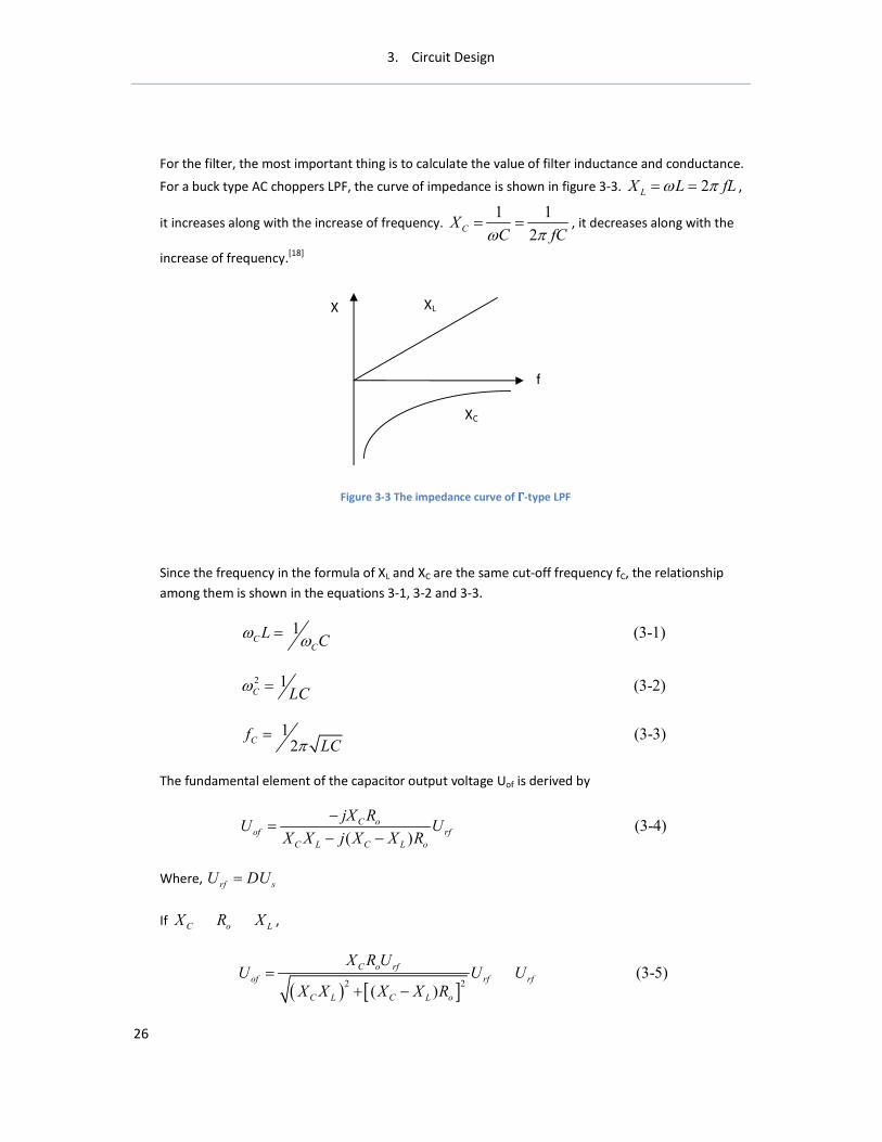
For the filter, the most important thing is to calculate the value of filter inductance and conductance.
For a buck type AC choppers LPF, the curve of impedance is shown in figure 3-3. 2LX L fLω π= = ,
it increases along with the increase of frequency. 1 1
2CX
C fCω π= = , it decreases along with the
increase of frequency.[18]
Since the frequency in the formula of XL and XC are the same cut-off frequency fC, the relationship
among them is shown in the equations 3-1, 3-2 and 3-3.
1 (3-1)CC
LC
ω ω=
2 1 (3-2)C LCω =
1 (3-3)2
CfLCπ
=
The fundamental element of the capacitor output voltage Uof is derived by
(3-4)( )
C oof rf
C L C L o
jX RU U
X X j X X R
−=
− −
Where, rf sU DU=
If C o LX R X� � ,
( ) [ ]22 (3-5)
( )
C o rf
of rf rf
C L C L o
X R UU U U
X X X X R
=+ −
�
Figure 3-3 The impedance curve of ΓΓΓΓ-type LPF
X XL
XC
f
3. Circuit Design
27
Their total harmonic distortion factors (THD) are defined as follows:
2
1
100[%] (3-6)V ok
kof
THD UU
∞
=
= ∑
Where Uok is the magnitude of the harmonic elements of the capacitor output voltage.
In this paper, the base frequency f1 is 50Hz, the lowest frequency of harmonic fk1 is 5kHz, and the cut-
off frequency fC is set as 500Hz.
Since f1 ≪ fC, 1
1
1L
Cω
ω� . So ω1L has a tiny resistance on base wave signal, and 1/ω1C has a
minimum split from base wave signal. Meanwhile, since fC≪fk1, 1
1
1k
k
LC
ωω
� . So ωk1L has a large
resistance on base wave signal, and 1/ωk1C has a large split from base wave signal. So the filter blocks
the lowest frequency of harmonic signal. And for the other harmonic signals which have higher
frequency, the filter will block them too.
The system parameters L and C are designed within the THD value required in the system. The
inductor and capacitor value can be obtained as:
2
1
100 2 (3-7)o
R THL
D THD
⋅=
⋅
1 1
2
(3-8)V o
THD THC
THD R TH
⋅=
⋅ ⋅
Since the inductor is chosen as 1mH already, the capacitor could be calculated as:
1 (3-9)100 2
V
TH DC
L THD
⋅=
⋅ ⋅
Where D is duty ratio,
2
1 2 61
1 sin
ks
kDTH
k
πω π
∞
=
= ∑
Considering other condition, such as the overheat of capacitor, the value of C couldn’t be to large.
Otherwise the impedance will be too small, since it depends on 1/ωC.
So the value to define for the capacitance is 0.22μF in the circuit.
3. Circuit Design
28
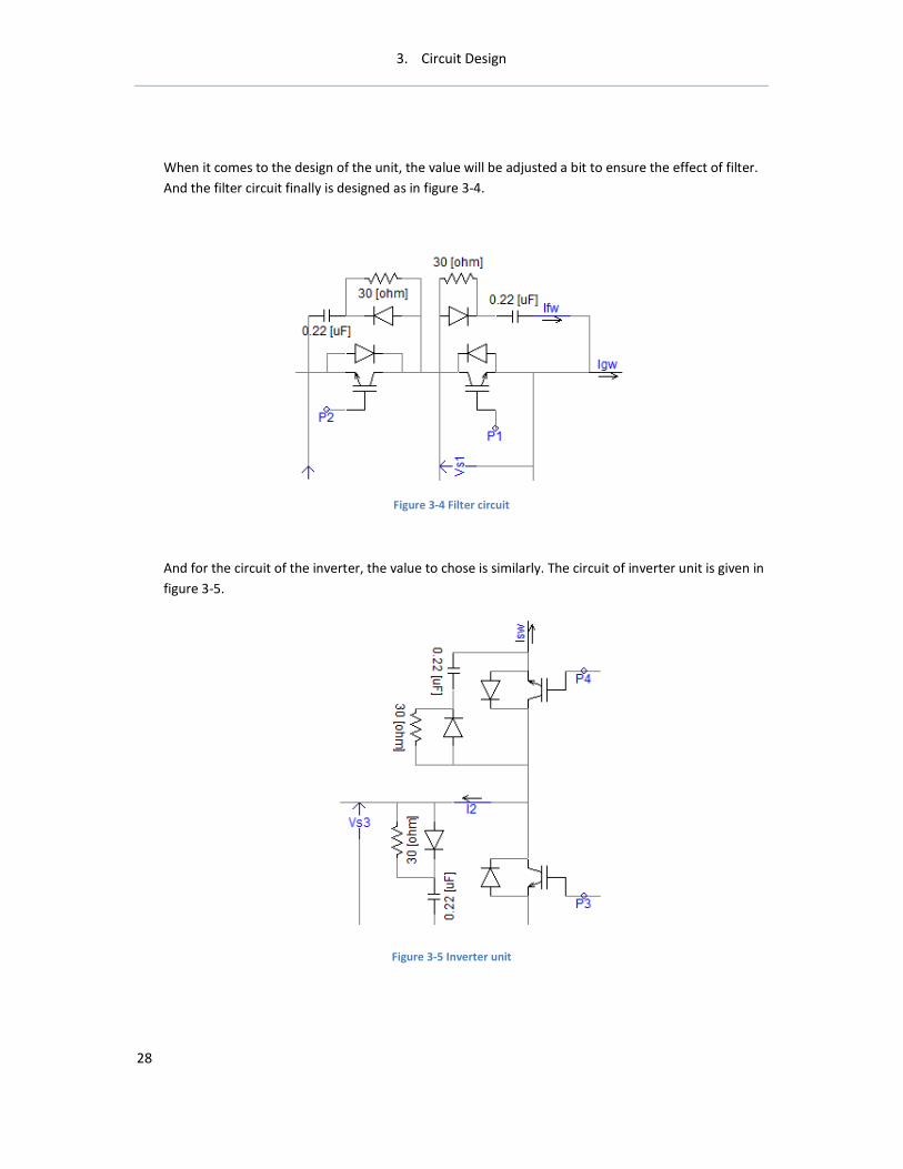
When it comes to the design of the unit, the value will be adjusted a bit to ensure the effect of filter.
And the filter circuit finally is designed as in figure 3-4.
Figure 3-4 Filter circuit
And for the circuit of the inverter, the value to chose is similarly. The circuit of inverter unit is given in
figure 3-5.
Figure 3-5 Inverter unit
3. Circuit Design
29
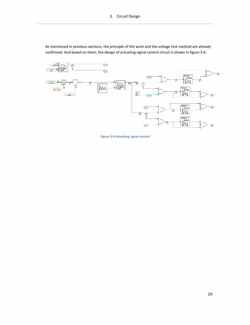
As mentioned in previous sections, the principle of the work and the voltage test method are already
confirmed. And based on them, the design of actuating signal control circuit is shown in figure 3-6.
Figure 3-6 Actuating signal control
4. Experiment and Simulation
30
4. Experiment and Simulation
4.1 General simulation result
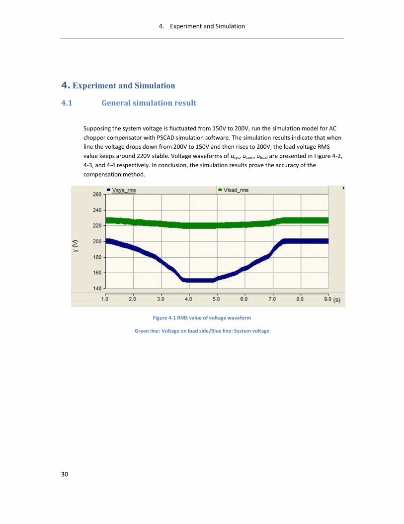
Supposing the system voltage is fluctuated from 150V to 200V, run the simulation model for AC
chopper compensator with PSCAD simulation software. The simulation results indicate that when
line the voltage drops down from 200V to 150V and then rises to 200V, the load voltage RMS
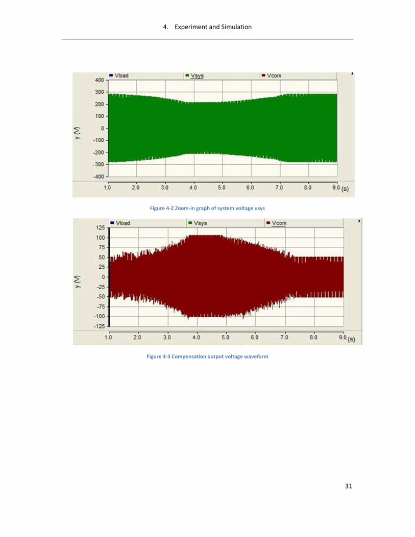
value keeps around 220V stable. Voltage waveforms of usys, ucom, uload are presented in Figure 4-2,
4-3, and 4-4 respectively. In conclusion, the simulation results prove the accuracy of the
compensation method.
Figure 4-1 RMS value of voltage waveform
Green line: Voltage on load side/Blue line: System voltage
4. Experiment and Simulation
31
Figure 4-2 Zoom-in graph of system voltage usys
Figure 4-3 Compensation output voltage waveform
4. Experiment and Simulation
32
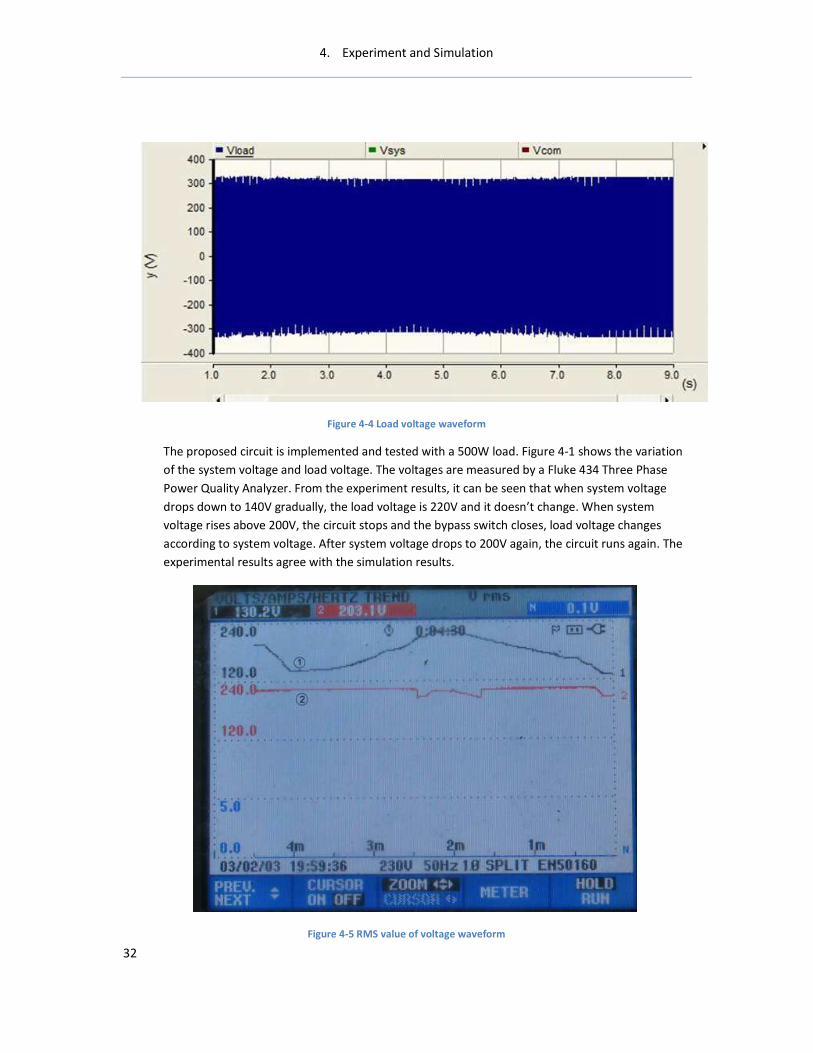
Figure 4-4 Load voltage waveform
The proposed circuit is implemented and tested with a 500W load. Figure 4-1 shows the variation
of the system voltage and load voltage. The voltages are measured by a Fluke 434 Three Phase
Power Quality Analyzer. From the experiment results, it can be seen that when system voltage
drops down to 140V gradually, the load voltage is 220V and it doesn’t change. When system
voltage rises above 200V, the circuit stops and the bypass switch closes, load voltage changes
according to system voltage. After system voltage drops to 200V again, the circuit runs again. The
experimental results agree with the simulation results.
Figure 4-5 RMS value of voltage waveform

4. Experiment and Simulation
33
4.2 Adjustment and advanced experiment
In this section, some adjustments on the circuit will be operated, and the influence could be
recognized by the simulation results. Actually, two experiments will be given in the next work.
The experiment to detect the influence of non-complementary control strategy is given first.
Experiment purpose: reduce the carrier wave frequency, detect whether the input voltage will fall
off when S1 turn on.
Program: LM_1126_01, duty cycle: 0.3, frequency: 500Hz
Measuring point:
Figure 4-6 Measuring point
A 100 ohm resistance is parallel with the primary winding of the isolating transformer which is
shown in figure 4-6. The current through the resistance is measured and the such measuring wave
is considered as the reference value for the isolating transformer primary winding. And the
positive half wave in CH2 is assumed as the output from the primary winding of the isolating
transformer.
Firstly, consider the case when the AC chopper does not operate, which means in positive half
wave, S1, S2 and S4 turn on, S3 turns off continued; in negative half wave, S1, S3, and S2 turn on,
S4 turn off continued. The output voltage is corresponding to the input voltage, without fall off
and loss. Observe the waveform.
The parameters are shown in table 4-1.
Input voltage(Vac) Inductance(mH) Conductance(μF) Resistance(Ω) Buffering circuit
15 2 100 1k Without S3, S4 buffer
Table 4-1 Parameters
4. Experiment and Simulation
34
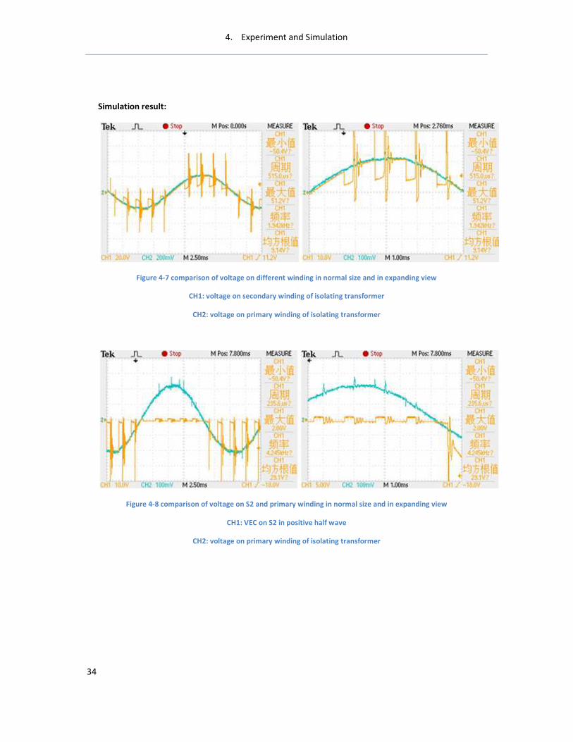
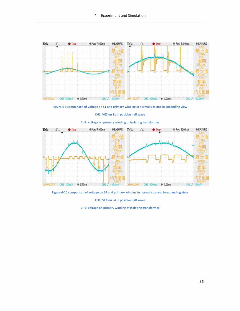
Simulation result:
Figure 4-7 comparison of voltage on different winding in normal size and in expanding view
CH1: voltage on secondary winding of isolating transformer
CH2: voltage on primary winding of isolating transformer
Figure 4-8 comparison of voltage on S2 and primary winding in normal size and in expanding view
CH1: VEC on S2 in positive half wave
CH2: voltage on primary winding of isolating transformer
4. Experiment and Simulation
35
Figure 4-9 comparison of voltage on S1 and primary winding in normal size and in expanding view
CH1: VEC on S1 in positive half wave
CH2: voltage on primary winding of isolating transformer
Figure 4-10 comparison of voltage on S4 and primary winding in normal size and in expanding view
CH1: VEC on S4 in positive half wave
CH2: voltage on primary winding of isolating transformer
4. Experiment and Simulation
36
Figure 4-11 comparison of voltage on S3 and primary winding in normal size and in expanding view
CH1: VEC on S3 in positive half wave
CH2: voltage on primary winding of isolating transformer
Figure 4-12 comparison of voltage on resistance and primary winding
CH1: voltage on the resistance
CH2: voltage on primary winding of isolating transformer

4. Experiment and Simulation
37
Figure 4-13 comparison of input voltage and voltage on primary winding in normal size and in expanding view
CH1: input voltage Vac
CH2: voltage on primary winding of isolating transformer
Figure 4-14 comparison of the peak value of input voltage and voltage in primary winding
CH1: peak value in figure 4-13
CH2: voltage on primary winding of isolating transformer
In figure 4-14, the dead zone of the expanding of peak is shown in the left one. And the dead zone
when S1 turns off is shown in the right one.

4. Experiment and Simulation
38
Figure 4-15
Figure 4-16
In figure 4-16, the peak of Vac is extreme high which is shown in the left one. And there is a partial
voltage seen from the wave in the right one when S1 turns on. The causation is that the
impedance of isolating transformer is too large, but the load impedance is not large enough.
When the voltage in primary winding is 11.5V, the voltage on the resistance is 7.5V. So the partial
voltage on the isolating transformer impedance is 4V. The leakage inductance is calculated in
equation 4-1:
40.0127( ) (4-1)
2 *50L H
π= =

4. Experiment and Simulation
39
The parameters are modified and are shown in table 4-2
Input voltage(Vac) Inductance(mH) Conductance(μF) Resistance(Ω) Buffering circuit
15 2 100|50|20 1k Without S3, S4 buffer
Table 4-2 Parameters
The conductance is reduced, and load resistance is increased in order to increase the partial
voltage on load and reduce the partial voltage on isolating transformer impedance.
Figure 4-17 comparison of input voltage Vac and output voltage in normal size and expanding view
CH1: input voltage Vac
CH2: output voltage from isolating transformer
The parameters are modified and are shown in table 4-3
Input voltage(Vac) Inductance(mH) Conductance(μF) Resistance(Ω) Buffering circuit
15 2 100|50|20 1k No
Table 4-3 Parameters
4. Experiment and Simulation
40
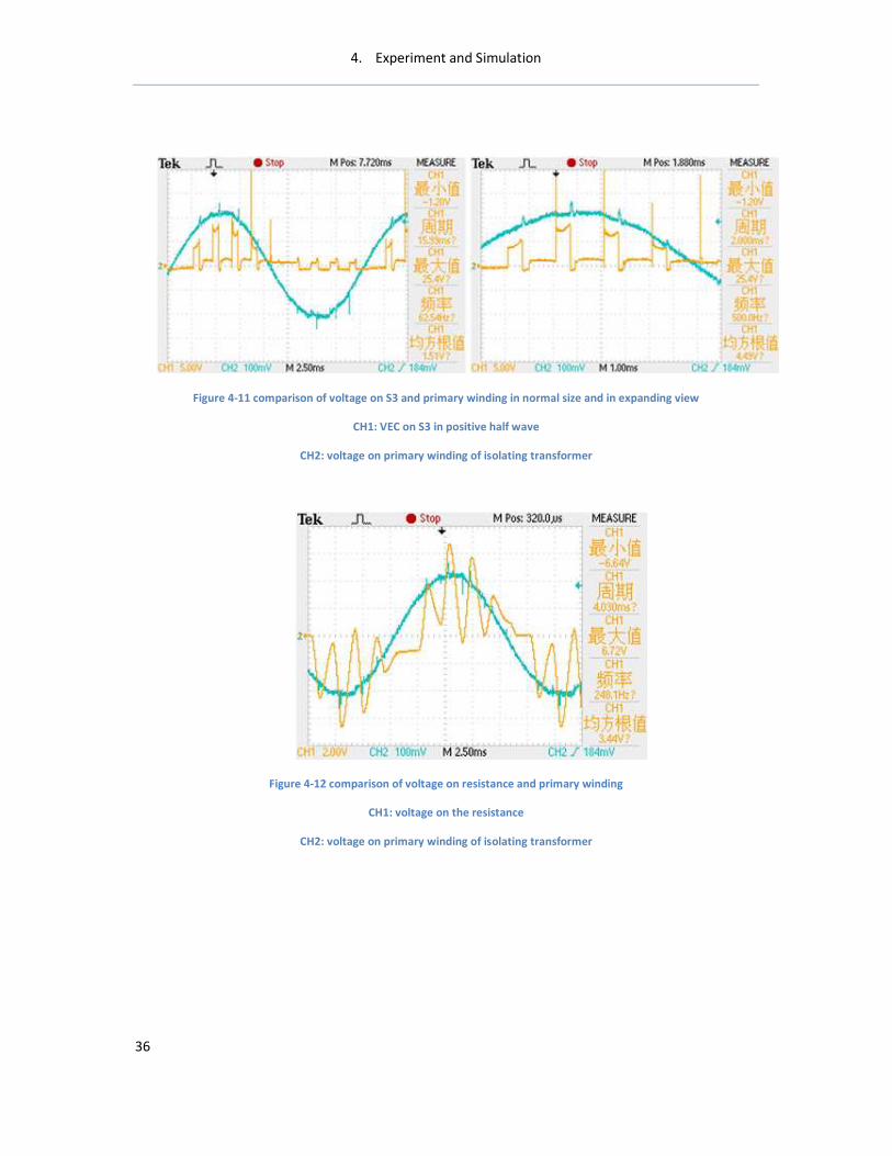
Figure 4-18 comparison of input voltage Vac and output voltage in normal size and expanding view
CH1: input voltage Vac
CH2: output voltage from isolating transformer
Seen from the right one of figure 4-18, the first peak is higher when the buffer circuit is removed,
and the oscillation is reduced.
Figure 4-19 Waveform when S3 or S1 turns off
The left one of figure 4-19 is the wave when S3 turns off. The oscillation of peak is about 10μs,
which is the dead zone.
The right one of figure 4-19 is the wave when S1 turns off. And the oscillation is totally
disordered.
On the whole, while the isn’t any conductance for compensating reactive power, the output
voltage of isolating transformer will fall off obviously when IGBT acts. And when the conductance
is added, the sag is compensated.

4. Experiment and Simulation
41
The experiment of duty cycle adjustment with load carried in given below.
Experiment purpose: Synchronization and loaded experiment, including AD sampling and duty
cycle adjustment.
Program: LV_1210_01, frequency 5kHz
Connecting way: input 380V, output 220V
Parameters are shown in table 4-4, when Vin=173V, Vload=221V
Parallel Conductance(μF) Inductance(mH) Conductance(μF) Load(W) Buffering circuit
25 (50 slots) 2 50 500 C=0.22μF, R=30Ω
Table 4-4 Parameters
Figure 4-20 Source voltage and its expanding graph
Seen from the figure 4-20, there are glitch at the peak.
Figure 4-21 Input voltage and its expanding graph
Seen from the figure 4-21, the input voltage is not smooth enough.
4. Experiment and Simulation
42
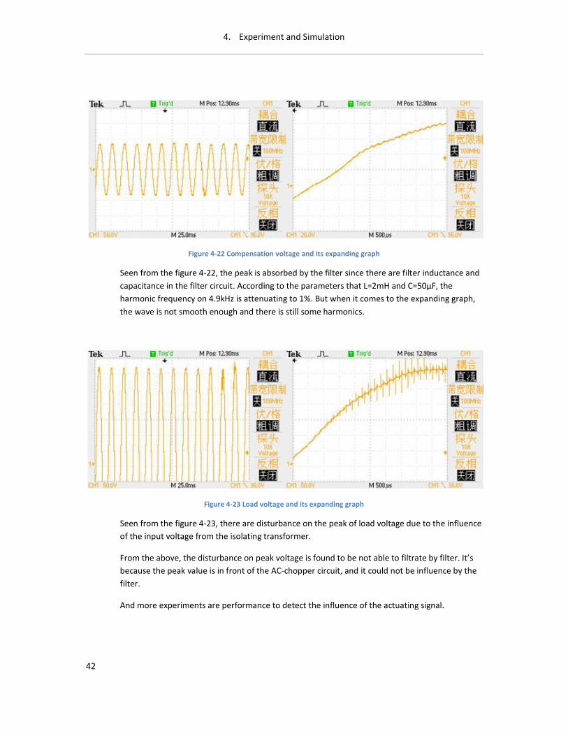
Figure 4-22 Compensation voltage and its expanding graph
Seen from the figure 4-22, the peak is absorbed by the filter since there are filter inductance and
capacitance in the filter circuit. According to the parameters that L=2mH and C=50μF, the
harmonic frequency on 4.9kHz is attenuating to 1%. But when it comes to the expanding graph,
the wave is not smooth enough and there is still some harmonics.
Figure 4-23 Load voltage and its expanding graph
Seen from the figure 4-23, there are disturbance on the peak of load voltage due to the influence
of the input voltage from the isolating transformer.
From the above, the disturbance on peak voltage is found to be not able to filtrate by filter. It’s
because the peak value is in front of the AC-chopper circuit, and it could not be influence by the
filter.
And more experiments are performance to detect the influence of the actuating signal.
4. Experiment and Simulation
43
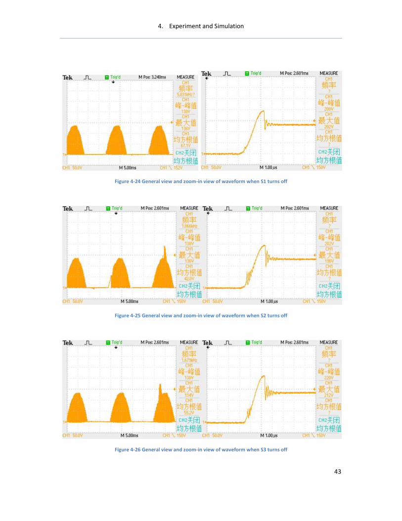
Figure 4-24 General view and zoom-in view of waveform when S1 turns off
Figure 4-25 General view and zoom-in view of waveform when S2 turns off
Figure 4-26 General view and zoom-in view of waveform when S3 turns off

4. Experiment and Simulation
44
Figure 4-27 General view and zoom-in view of waveform when S4 turns off
Seen from four figures shown above, there is too much oscillation when S2, S3 and S4 turn off.
4.3 Conclusion
This thesis proposed a voltage compensator based on an AC buck chopper, which is operated using the
strategy of non-complementary control without current detection. It is suitable for compensation long-
term voltage sags and could adjust pulse widths according to the ratio of required output in real time.
Simulations and experiment results proved functionality of this circuit. The only drawback of the circuit is
that PWM pulsations will produce harmonic current. We will settle this problem in the next work
additionally.
4.4 Harmonic analysis
System voltage is defined as follow:
0sin(2 ) (4-2)sys mu U f tπ=
where Um and f0 are the magnitude and frequency of the system voltage. The output ucom is expressed as
follow:
( ) (4-3)com sysu S t u= ×
where S(t) is switching function expressed as:
1( ) 0, 1, 2 (4-4)
0 ( 1)
s s s
s s s
nT t nT DTS t n
nT DT t n T
≤ ≤ += = ± ± ⋅⋅⋅
+ ≤ ≤ +
4. Experiment and Simulation
45
where Ts is switching period. The Fourier series of ucom by substitution of (4-2) and (4-3) into (4-5) is
obtained:
}{0 0 0
1
sinsin(2 ) sin[2 ( ) ] sin[2 ( ) ] (4-5)m
com m s s
m
Uu DU f t mf f t mf f t
m
απ π α π α
π
∞
=
= + + − − − −∑
where fs is frequency of PWM, and m Dα π= . It is indicated that there were harmonic in ucom, the
frequency of harmonic distributes at mfs±f0. Felting harmonic voltage improving switching frequency and
varying L and C2 are useful for felting harmonic voltage.

Acknowledgement
46
Acknowledgement
First of all I would like to express my highest appreciated to all the people that give me so much help
during the whole period of this project. Professor Liu Kaipei and Dr. Su yi at Wuhan University
support me a lot in the summer, and I wasn’t able to finish this thesis work without their guidance
and experience shared.
I also want to show my sincere gratitude to my thesis supervisor and examiner at KTH – Hans Peter
Nee for his continuously support and encouragement.
Especially, I will thank my girlfriend Chenjie who is always encourage me and inspire me all of these
days.
Finally, special thanks are expressed to my parents for their endless support and love.
Stockholm, 3rd
/Sep. 2009
Kai Wang
Reference
47
Reference
[1] Ned Mohan, Tore M. Undeland and Willam P. Robbins, Power Electronics. John Wiley & Sons, INC. United States, 2003.
[2] IEEE Standard board. IEEE Std 1159-1995: IEEE Recommended Practice for Monitoring Electric Power Quality. The
Institute of Electrical and Electronics Engineers, Inc. 1995, Page(s):11~23
[3] M. Bollen, Understanding Power Quality Problem, Voltage Sags and Interruption, Piscataway, NJ: IEEE Press, 1999.
[4] Alex McEachern, http://www.powerstandards.com/tutorials/sagsandswells.htm, Power Standards Lab. 2004
[5] Arrillaga, J.; Bollen, M.H.J.; Watson, N.R, Power quality following deregulation, Proceedings of the IEEE, Vol.88 No.2,
Page(s): 246-261, Feb. 2000.
[6] Yang Honggen, Xiao Xianyong, Liu Junyong, Power Quality Problem Research and Technique (Three)-Voltage Sags in
Power System, Power Electrical Equipment. No.12, 2003.
[7] Zhao He, Zhou Xiaoxin, Wu Shouyuan, Compensation of Power Network to Improve Power Quality, Electrical
Equipment. Vol. 4, No. 1, February, 2003.
[8] Hingorani NG, Introducing Custom Power, IEEE Spectrum, 1995, 12(2), Page(s): 41~48
[9] You Yong, Han Mingxiao, The Implementation of Dynamic Voltage Restorer, Power system automation, 2003, 21(27).
[10] Arindam Ghosh, Gerard Ledwich, STRUCTURES AND CONTROL OF A DYNAMIC VOLTAGE REGULATOR,
IEEE, 2001, Page(s): 1027~1031.
[11] Wang Kaifei, Li Yandong, Research on continuous three phase dynamic voltage regulator, Power Electronics.
[12] Tang Zhi, Yang Chao, Ma Weixin, Design on series power compensation circui,. Power system automation, Vol. 26, No.19,
Oct, 10, 2002.
[13] B.H.Li, S.S.Choi and D.M. Vilathgamuwa, Transformerless dynamic voltage restorer, IEE Proc-Gener, Transm. Distrib.
Vol. 149, No.3, May 2002.
[14] Huang Han, Yang Chao, Han Yingyi, Reseauch on control strategy of Dynamic Voltage Restorer, Power system technique,
Vol.26, No.1, 2002.
[15] Santo, Grady W M, Characterization of distribution power quality events with Fourier and wavelet transforms, IEEE Trans
on Power Delivery, 2000, 15(1), Page(s): 247~254.
[16] Chung Jaehak, Powers EJ, An automatic voltage sag detector using a discrete wavelet transform and a CFAR detector, PES
Summer Meeting, 2001. Vol 1(1), Page(s): 689~693.
[17] Nabil A Ahmed, Kenji Amei, and Masaaki Sakui, A New Configration of Single-Phase Symmetrical PWM AC Chopper
Voltage Controller, Transaction of IEEE on Industrial Electronics, Vol.46, No.5, October 1999, Page(s): 942~952.
[18] Chen Daolian, DC-AC inversion technique and application, Machinery Industry Press(2006), Page(s): 223~225.
Acknowledgement
48
[19] Y, Okuma. PWM Controlled AC Power Supply based on AC Chopper Technology and Its Applications, Transaction of
IEE Japan Vol.199-D, No.3, 1999, Page(s): 412-418.
[20] PSCAD/EMTDC User’s Guide, Page(s): 3~5.