
ANALYSIS AND PWM CONTROL OF SWITCHED BOOST INVERTER …docs.neu.edu.tr/library/6727769928.pdf ·...
84
ANALYSIS AND PWM CONTROL OF SWITCHED BOOST INVERTER A THESIS SUBMITTED TO THE GRADUATE SCHOOL OF APPLIED SCIENCES OF NEAR EAST UNIVERSITY By TARIQ MOHAMMED ATEEYAH MOHAMMED In Partial Fulfillment of the Requirements for the Degree of Master of Science in Electrical and Electronic Engineering NICOSIA, 2019 TARIQ MOHAMMED ATEEYAH ANALYSIS AND PWM CONTROL OF NEU MOHAMMED SWITCHED BOOST INVERTER 2019
Transcript of ANALYSIS AND PWM CONTROL OF SWITCHED BOOST INVERTER …docs.neu.edu.tr/library/6727769928.pdf ·...

ANALYSIS AND PWM CONTROL OF SWITCHED BOOST
INVERTER
A THESIS SUBMITTED TO THE GRADUATE SCHOOL OF APPLIED SCIENCES
OF NEAR EAST UNIVERSITY
By
TARIQ MOHAMMED ATEEYAH MOHAMMED
In Partial Fulfillment of the Requirements for the Degree of Master of Science
in Electrical and Electronic Engineering
NICOSIA, 2019
TA
RIQ
MO
HA
MM
ED
AT
EE
YA
H A
NA
LY
SIS
AN
D P
WM
CO
NT
RO
L O
F N
EU
MO
HA
MM
ED
SW
ITC
HE
D B
OO
ST
INV
ER
TE
R 2
019

ANALYSIS AND PWM CONTROL OF SWITCHED BOOST
INVERTER
A THESIS SUBMITTED TO THE GRADUATE
SCHOOL OF APPLIED SCIENCES
OF
NEAR EAST UNIVERSITY
By
TARIQ MOHAMMED ATEEYAH MOHAMMED
In Partial Fulfillment of the Requirements for
the Degree of Master of Science
in
Electrical and Electronic Engineering
NICOSIA, 2019

I hereby declare that all information in this document has been obtained and presented in accordance with
academic rules and ethical conduct. I also declare that, as required by these rules and conduct, I have fully
cited and referenced all material and results that are not original to this work.
Name: Tariq Mohammed Ateeyah Mohammed
Signature:
Date:

i
ACKNOWLEDGEMENTS
First, I would like to thank Allah and to express my deep and sincere gratitude to my thesis
advisor Prof. Ebrahim Babaei for his excellent supervision and helps during this work. It is a
pleasure for me to take the opportunity to thank all my colleagues also for support.
Moreover, my deep thanks to all my family to fully support.

ii
ABSTRACT
The Z source inverter or impedance source inverter is derived by placing an impedance network composed
of inductor and capacitor with symmetrical features between the power and the inverter bridge of voltage
and current source inverters. Some the distinctive attributes of the impedance source inverter when
employed in power conditioning is the ability to function either as buck inverter, boost inverter or buck-
boost inverter, immunity to the negative effects of EMIs, useful for renewable energy applications due to
its wide peak to peak power functionality. Despite the numerous advantages of ZSI over VSI/CSI, the
size, weight and cost of ZSI is of great concern and this is caused by the size of the impedance network
components. The switched boost inverter topology which possesses all the advantages of the traditional
impedance source inverter (ZSI) but with reduced passive component count and an increase in the number
of required active components. Simulation and mathematical analysis of the switched boost inverter
topology is carried out the environs of PSCAD software and results produced. Two types of PWM control
techniques are utilized in the control of the SBI topology during simulation.
Keywords: Z source inverter; boost factor; switched boost inverter; PWM; buck inverter

iii
ÖZET
Z kaynağı inverteri ya da direnç kaynak inverteri, voltaj ve akım kaynağı inverterlarının inverter köprüsü
ve gücü arasında simetrik özellikleri olan kapasitör ve endüktörden oluşan direnç ağından elde edilir. Güç
düzenleyici üniteler uygulandığı zaman oluşan direnç kaynağı inverterinin önemli özelliklerinden bazıları
buck inverter, boost inverter veya buck-boost inverter gibi işleyebilme yeteneği EMI’lerin olumsuz
etkilerine karşı bağışıklığı ve geniş zirveden zirveye güç işlevselliğine bağlı yenilenebilir enerji
uygulamaları için kullanışlı olmalarıdır. VSI/CSI'ye göre ZSI’nin birçok avantajı olmasına rağmen,
ZSI’nin boyutu, ağırlığı ve fiyatı büyük bir problem ve bu direnç ağı bileşenlerinden kaynaklanmaktadır.
Kurmalı boost inverter topolojisi geleneksel direnç ağı inverterinin (ZSI) tüm avantajlarını, indirgenmiş
pasif bileşen ve artırılmış gerekli aktif bileşen miktarını kapsamaktadır. Kurmalı itiş inverter topolojisinin
simulasyon ve matematiksel analizi PSCAD yazılımı kullanılarak yapılmıştır ve sonuçlar elde edilmiştir.
PWM kontrol tekniklerinin iki türü, simulasyon süresince SBI topoloji kontrolüyle kullanılmıştır.
Anahtar kelimeler: Z kaynağı inverteri; boost Faktörü; kurmalı boost inverteri; PWM; buck inverteri

iv
TABLE OF CONTENTS
ACKNOWLEDGEMENTS ............................................................................................................... i
ABSTRACT ....................................................................................................................................... ii
ÖZET ................................................................................................................................................ iii
TABLE OF CONTENTS ................................................................................................................... iv
LIST OF TABLE ............................................................................................................................... vi
LIST OF FIGURES .......................................................................................................................... vii
LIST OF ABBREVIATIONS ............................................................................................................. ix
CHAPTER 1 INTRODUCTION
1.1 General Concept .................................................................................................................................... 1
1.2 Thesis Problem ...................................................................................................................................... 3
1.3 The aim of Thesis .................................................................................................................................. 3
1.4 The importance of Thesis ...................................................................................................................... 4
1.5 Limitation of study ................................................................................................................................ 4
1.6 Overview of the Thesis ......................................................................................................................... 4
CHAPTER 2 LITERATURE REVIEW
2.1 Introduction ........................................................................................................................................... 5
2.2 Z source inverter ................................................................................................................................... 5
2.3 Z Source Matrix Converter ................................................................................................................... 8
2.4 MCZS .................................................................................................................................................. 10
2.5 Quasi ZSI ............................................................................................................................................ 12
2.6 Impedance Source Rectifier ................................................................................................................ 14
2.7 Z-H Buck Converter ........................................................................................................................... 15
2.8 ZS-HB Converter ................................................................................................................................ 17
2.9 Trans and Quasi Topologies ............................................................................................................... 20
2.10 Z Source dc-dc Converter ................................................................................................................... 23
2.11 qZSI Based 1ph to 3ph ........................................................................................................................ 33
2.12 qZSI + T-type Inverter ........................................................................................................................ 35
2.13 Quasi Z Source Multipoint Converter ................................................................................................. 37
2.14 qSBZS+T-type .................................................................................................................................... 39
2.15 Quasi Switched Boost Cascaded HB Inverter ..................................................................................... 41
2.16 Quasi switched Boost dc-dc Converter ............................................................................................... 43
2.17 SC/qSBI .............................................................................................................................................. 43
2.18 SCL/qZSI ............................................................................................................................................ 46

v
2.19 Conclusion .......................................................................................................................................... 49
CHAPTER 3 POWER CIRCUIT DESCRIPTION AND SIMULATION RESULTS
3.1 Introduction ........................................................................................................................... 50
3.2 Chosen Topology .................................................................................................................... 50
3.3 Conclusion ............................................................................................................................. 54
3.4 Switch Boost Inverter Controlled by PWM ................................................................................ 54
3.5 Simulation Results .................................................................................................................. 57
CHAPTER 4 CONCLUSION AND RECOMMENDATIONS
4.1 Conclusion ............................................................................................................................. 61
4.2 Recommendations ................................................................................................................... 63
REFERENCES ................................................................................................................................ 64

vi
LIST OF TABLE
Table 2.1: Current of each Component in Different States .............................................................................. 26
Table 2.2: Comparison on Number of Component .......................................................................................... 27
Table 2.3: Comparison of Switch Stress .......................................................................................................... 27
Table 2.4: Comparison of Diode Stress ........................................................................................................... 28
Table 2.5: Comparison between Proposed ZIMPC and conventional ASHB Topology ................................. 38
Table 2.6: Switching States of the Proposed QSBT2I (x=a, b, c)..................................................................... 40
Table 2.7: Comparison of the three–level QSBT2I with other impedance–source –based three level inverter 41
Table 2.8 : Comparison between cascaded five – level qSBI and qZSI .......................................................... 42
Table 2.9: Comparison of selected transformer type impedance source inverters ........................................... 48
Table 3.1: Simulation Parameters .................................................................................................................... 58
vii
LIST OF FIGURES
Figure 1.1: Voltage source inverter .................................................................................................................. 2
Figure 1.2: Current source inverter ................................................................................................................... 3
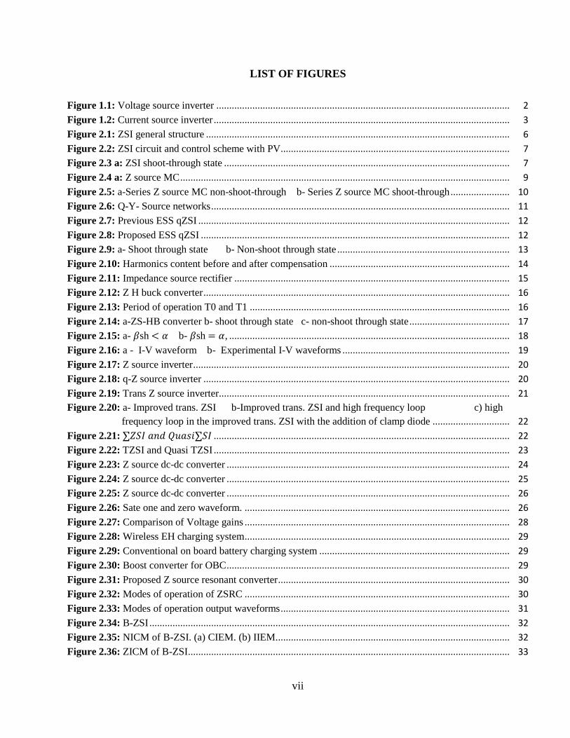
Figure 2.1: ZSI general structure ...................................................................................................................... 6
Figure 2.2: ZSI circuit and control scheme with PV ......................................................................................... 7
Figure 2.3 a: ZSI shoot-through state ............................................................................................................... 7
Figure 2.4 a: Z source MC ................................................................................................................................ 9
Figure 2.5: a-Series Z source MC non-shoot-through b- Series Z source MC shoot-through ....................... 10
Figure 2.6: Q-Y- Source networks .................................................................................................................... 11
Figure 2.7: Previous ESS qZSI ......................................................................................................................... 12
Figure 2.8: Proposed ESS qZSI ........................................................................................................................ 12
Figure 2.9: a- Shoot through state b- Non-shoot through state ................................................................... 13
Figure 2.10: Harmonics content before and after compensation ...................................................................... 14
Figure 2.11: Impedance source rectifier ........................................................................................................... 15
Figure 2.12: Z H buck converter ....................................................................................................................... 16
Figure 2.13: Period of operation T0 and T1 ..................................................................................................... 16
Figure 2.14: a-ZS-HB converter b- shoot through state c- non-shoot through state ....................................... 17
Figure 2.15: a- 𝛽sh < 𝛼 b- 𝛽sh = 𝛼, ............................................................................................................. 18
Figure 2.16: a - I-V waveform b- Experimental I-V waveforms ................................................................. 19
Figure 2.17: Z source inverter ........................................................................................................................... 20
Figure 2.18: q-Z source inverter ....................................................................................................................... 20
Figure 2.19: Trans Z source inverter................................................................................................................. 21
Figure 2.20: a- Improved trans. ZSI b-Improved trans. ZSI and high frequency loop c) high
frequency loop in the improved trans. ZSI with the addition of clamp diode .............................. 22
Figure 2.21: ∑𝑍𝑆𝐼 𝑎𝑛𝑑 𝑄𝑢𝑎𝑠𝑖∑𝑆𝐼 ................................................................................................................... 22
Figure 2.22: TZSI and Quasi TZSI ................................................................................................................... 23
Figure 2.23: Z source dc-dc converter .............................................................................................................. 24
Figure 2.24: Z source dc-dc converter .............................................................................................................. 25
Figure 2.25: Z source dc-dc converter .............................................................................................................. 26
Figure 2.26: Sate one and zero waveform. ....................................................................................................... 26
Figure 2.27: Comparison of Voltage gains ....................................................................................................... 28
Figure 2.28: Wireless EH charging system ....................................................................................................... 29
Figure 2.29: Conventional on board battery charging system .......................................................................... 29
Figure 2.30: Boost converter for OBC .............................................................................................................. 29
Figure 2.31: Proposed Z source resonant converter .......................................................................................... 30
Figure 2.32: Modes of operation of ZSRC ....................................................................................................... 30
Figure 2.33: Modes of operation output waveforms ......................................................................................... 31
Figure 2.34: B-ZSI ............................................................................................................................................ 32
Figure 2.35: NICM of B-ZSI. (a) CIEM. (b) IIEM........................................................................................... 32
Figure 2.36: ZICM of B-ZSI ............................................................................................................................. 33

viii
Figure 2.37: qZSI based 1ph to 3ph .................................................................................................................. 34
Figure 2.38: a- shoot through mode b- non shoot through mode .................................................................. 34
Figure 2.39: qZSI + T type inverter .................................................................................................................. 36
Figure 2.40: qZSI + T type inverter fault mode ................................................................................................ 37
Figure 2.41: qZSI + T type inverter fault mode ................................................................................................ 37
Figure 2.42: qZIMPC ........................................................................................................................................ 38
Figure 2.43: qZSAHB ....................................................................................................................................... 38
Figure 2.44: qSBZS+T-type ............................................................................................................................. 39
Figure 2.45: Modes of operation of qSBZS+T-type ......................................................................................... 40
Figure 2.46: qSBCHBI ..................................................................................................................................... 41
Figure 2.47: a- Shoot through b- Non-shoot through....................................................................................... 42
Figure 2.48: Quasi switched boost dc-dc converter .......................................................................................... 43
Figure 2.49: SC/qSBI a- type 1 b- type 2 ................................................................................................... 44
Figure 2.50: Operational states of SC/qSBI ...................................................................................................... 45
Figure 2.51: Multicell structure of SC/qSBI ..................................................................................................... 46
Figure 2.52: SCL/qZSI ..................................................................................................................................... 47
Figure 2.53: a- Shoot through b- Non-shoot through........................................................................................ 47
Figure 3.1: Switched boost inverter .................................................................................................................. 50
Figure 3.2: a- shoot through b- non-shoot through ......................................................................................... 51
Figure 3.3: Clarified switch boost inverter circuit. ........................................................................................... 51
Figure 3.4: a- SBI stable state waveforms b- SBI duty ratio ....................................................................... 52
Figure 3.5: Conventional PWM control signals................................................................................................ 55
Figure 3.6: Modified PWM control signals ...................................................................................................... 55
Figure 3.7: Control circuit of modified PWM .................................................................................................. 56
Figure 3.8: Shoot through waveform ................................................................................................................ 56
Figure 3.9: SBI circuit for simulation ............................................................................................................... 57
Figure 3.10: SBI circuit for simulation ............................................................................................................. 58
Figure 3.11: SBI circuit for simulation ............................................................................................................. 59
Figure 3.12: SBI circuit for simulation ............................................................................................................. 59
Figure 3.13: SBI circuit for simulation ............................................................................................................. 60

ix
LIST OF ABBREVIATIONS
VSI Voltage Source Inverter
FACTS Flexible alternating current transmission system
CSI Current Source Inverter
ZSI Impedance Source Network
BZSI Bidirectional Impedance Source Network
IZSI Improved Z Source Inverter
PV Photovoltaic Systems
HPZSI High Performance Impedance Source Network
EMI Electromagnetic Interference
FLZSI Four Leg Z Source Inverter
DuZSI Dual Z Source Inverter
NPZSI Neutral Point Z Source Inverter
ZSID Z Source Inverter Diode
ZSIS Z Source Inverter Switch
QZSI Quasi-Z-Source Inverter
SLQZSI Switched Inductor Quasi-Z-Source Inverter
DGC Doubly Grounded Circuits
HFTI High Frequency Transformer Isolation
PWM Pulse Width Modulation
CB Circuit Breakers
UC Ultra-Capacitor
CFSI Current Fed Switched Inverter
KVL Kirchhoff Voltage Low
RL Resistive-Inductive SBI Impedance Based Inverter
MC Matrix Converters
PSC Phase Shift Control
CIEM Complete Inductor Energy-supplying Mode
IIEM Incomplete Inductor Energy-supplying Mode
ZPCM Zero-crossing Input Current Mode
NPCM Non-zero-crossing Input Current Mode
ZICM Zero-crossing Inductor Current Mode
NICM Non-zero-crossing Inductor Current Mode
DC Direct Current
AC Alternating Current

1
CHAPTER 1
INTRODUCTION
1.1 General Concept
The process of changing dc voltage/power to ac voltage/power is known as inversion; this process is
realized by the use of principal device called an inverter. The first inverter is commonly known as the
conventional 2-level inverter which is a voltage source inverter- VSI. The function of the conventional 2-
level inverter is to utilize a fixed source voltage to provide changeable frequency/voltage at the inverter
output for use by varied applications such as adjustable speed drive etc. inverters are classified into two
groups from the input/source point of view and these categories are current source inverter CSI and
voltage source inverter VSI.
A voltage source inverter is an inverter in which the source voltage (dc) amplitude is constant and it is
not affected by the current of the load. Basically the output voltage is dependent on the characteristics of
the inverter and the current value is dependent on the type of load. Voltage source inverters have wide
areas of applications because the input is voltage source and it is suitable for many applications which
require voltage source as the input. Variable or adjustable speed drives and FACTS devices are some
major the major applications of voltage source inverters. Although VSI can be applied high power system,
it is most suitable in medium power applications because they are able to generate output voltage with
very high quality waveforms. The dc input voltage of a voltage source inverter can be any of the
following; capacitor, battery, rectifier circuit source, fuel cell, PV systems etc. in the case of multilevel
inverters where multiple dc source are required, a combination of the above sources can be utilized. A
common type of VSI circuit is the single phase H Bridge inverter with four switches each connected with
an anti-parallel diode, this switch topology allows for current flow in bi-direction and unidirectional
voltage flow.
The voltage source inverter also known as voltage source converter (when used for both inversion and
rectifying purposes) has wide areas of applications but it’s fraught with many limitations such:
It’s a buck or step down inverter that’s the output voltage is always less than the input voltage unless a
buck-boost converter is applied. When used as a rectifier, it’s a boost rectifier circuit.
a. Applications of buck-boost converter in VSI topology increases the cost of the unit, reduces the
efficiency of the system and complicated control technique is introduced.
b. Shoot through property is absent in VSI or CSI hence EMIs immunity is absent

2
c. Inductor – capacitor filter is required to reduce power systems noises.
On the other hand, the current source inverter or converter is achieved by putting a large inductor in series
with the dc source. Just as in the case of voltage source inverter, the dc input voltage of a current source
inverter can be any of the following; capacitor, battery, rectifier circuit source, fuel cell, PV system. Figure
1.1 and Figure 1.2 show the circuit diagram of voltage and current source inverters. These topologies are
similar but have differences in the type of source voltage and the type of switches used. The difference in
switch types is because in the VSI; bidirectional current flow and unidirectional voltage flow is required
whilst in the CSI; bidirectional voltage flow is required and unidirectional current flow is required. In the
case of CSI, several switch types can be utilized to achieve bidirectional voltage flow and unidirectional
current flow, some examples of such switches are: SCR, series connection of IGBT and diode, GTO,
SCR. Some limitations of CSI are:
a. The current source inverter is a boost inverter and when applied as rectifier, it’s a buck rectifier
circuit.
b. Buck dc converters are required to reduce the cost hence, cost of system and efficiency increases
and reduces respectively.
c. Open circuit on a load side is a big problem when preventive measures are not taken and reverse
voltage path should be provide or blocked.
Figure 1.1: Voltage source inverter

3
Figure 1.2: Current source inverter
1.2 Thesis Problem
Voltage source inverters and current source inverters have revolutionized power conditioning for
industrial applications in varied areas of the engineering fields. Also they have contributed immensely to
development of inverters most especially multilevel inverters. The quality of their output waveforms is
good and they have wide range of applications. Although VSI and CSI are very useful in industrial
applications, they are still bedeviled some drawbacks which when eliminated can improve their
efficiency.
The major limitations of these converters have enumerated in the introduction section of this chapter. The
introduction of Z source or impedance networks into VSI and CSI solves the problems of buck or boost
quality depending on the topology and also shoot through property provides immunity to the effects of
EMIs. The conventional Z source based inverter solves major drawbacks of VSI and CSI but they also
introduce some limitations such as increased cost and size hence they are not appropriate for use in low
power systems when they following factors are off great concern; cost, weight and size.
1.3 The aim of Thesis
The primary aim of this thesis is to provide solutions to the disadvantages of voltage source inverter,
current source and conventional Z source based inverters in application areas where size, weight and cost
are major factors for the system designing. This is achieved by introducing a novel impedance based
inverter called SBI; switched Boost inverter. This inverter has the advantage of the conventional Z source
inverter plus its own advantages such as reduced passive
Component count but increased active component count hence better control of the circuit. Analysis of
the proposed inverter will be carried in two phases; a. steady state and b. small signal.

4
1.4 The importance of Thesis
It’s evident that power conditioning units such as power electronic converters have come to stay are
contributing immensely to development of power systems. They are used in almost every sphere of human
endeavor. Some notable application areas of power electronics are: transportation, space technology,
utility systems, industrial settings and home appliances.
The efficient and effective use of power electronic converters to produce good quality waveforms as
desired by loads is the importance of this research. This will result in minimizing loses, increase efficiency
thereby driven down the cost of power for the consumer, efficient use of power source will increase the
lifespan of source and also reduce monopoly in marketing.
1.5 Limitation of study
Even though this research was conducted with outermost care, the possibilities of shortcomings and
limitations are unavoidable. First the research was conducted using EMTDC/PSCAD software hence the
ability to control the research is limited to the mathematical modeling of the software. Although research
based simulation results have become an acceptable standard in academia, the disadvantage of not having
experimental results due cost of components, proper practical knowledge and conducive laboratory cannot
be ignored.
1.6 Overview of the Thesis
The structure of this thesis is as follows:
Chapter 1: Introduction. This chapter is made of introduction, Thesis Problem, The aim of Thesis, The
important of Thesis and overview of the thesis.
Chapter 2: Literature Review of Z Source Inverters Chapter 3: Power Circuit Description and
Simulation Results Chapter 4: Conclusion and Future Works

5
CHAPTER 2
LITERATURE REVIEW
2.1 Introduction
The goal of this literature review is to review previously published papers on Z-Source inverters
popularly known as ZSI. The review will consider the various topologies that have been developed after
the introduction of the main ZSI topology, their applications and usefulness in industry when compared
to other inverter topologies; the various control methodologies which are applicable to ZSI and other
factors which makes the ZSI a suitable inverter for power electronics applications.
2.2 Z source inverter
The impedance structure or Z source system was basically developed to overcome the limitations
associated with conventional voltage or current source converters/inverters, dc-dc converters and
bidirectional and unidirectional converters. The main attraction of the impedance structure lies in its
flexible source characteristics and the ability to increase output voltage from 0 to infinity theoretically.
Different topologies of Z source structure have developed to increase the voltage gain or boosting factor
of the converter and also limit stress imposed on the semiconductor switches whiles maintaining the
basic structure of Z source system. These topologies are classified according to the following categorizes
listed below and the magnetically coupled type seems promising because least number of electronic
components are used and also higher voltage gain is achieved using only short ratio of duty cycle during
the short-through state .
Switched device technique.
Cascading methodology.
Magnetically coupled methodology.
The authors in (Xu, P., Zhang, X., Zhang, C. W., Cao, R. X., & Chang, L, 2006) studies the application
of ZSI in photovoltaic systems; the disadvantages of voltage source inverters such as; random
fluctuations in generated photovoltaic power means that buck or boost or a combination of the two;
buck-boost converter is required for injected grid power stability which increases the cost of the system
and also reduces the efficiency of the system, shoot through scheme is not applicable but dead-time
control method is rather employed and this results in distorted output current waveforms. Other
disadvantage reported in (Peng, F. Z., Yuan, X., Fang, X., & Qian, Z, 2003) is an output filter is required
6
to produce quality output power which also leads to more losses. All the problems enumerated above
concerning the VSI are solved by the introduction of the ZSI topology. The Z source inverter or
converter for general forms of power conversion is the utilization of an impedance network between the
voltage source and the main converter circuitry. The impedance network is made up of two passive
components; inductors and capacitors, other improved impedance network reduces the number of
passive components and applies active component instead. In photovoltaic applications, a diode is
connected in series with the panels to protect the panels from reverse current from the load because the
PV panels are not energy storage systems i.e. unable to store dc voltage. The ZSI topology was
developed by (Peng, F. Z., Yuan, X., Fang, X., & Qian, Z, 2003) in 2003 and after since several
improved ZSI circuitry have been developed. Figure 2.1 shows the main ZSI developed by (Peng, F. Z.,
Yuan, X., Fang, X., & Qian, Z, 2003). The main advantage of the ZSI over other inverter topologies
such as VSI or CSI is the shoot through characteristics which when controlled properly can increase or
decrease the magnitude of the input voltage for both ac and dc voltages respectively. The shoot through
attribute of the ZSI eliminates the need for the dead time hence the inverter output current is devoid of
distortions increasing the quality of the produced power (Xu, P., Zhang, X., Zhang, C. W., Cao, R. X.,
& Chang, L, 2006).
Figure 2.1: ZSI general structure
Basic analysis of ZSI when connected to PV system is done in (Xu, X. Zhang, et al, 2006) which will
be grid tied at the converter output. This analysis is achieved by designing a suitable control scheme for
the setup, the ZSI capacitor voltage and grid current is regulated by controlling the modulation index,
the shoot through property is regulates the PV output voltage. Figure 2.2 shows the ZSI based
photovoltaic system which includes the control scheme. Certain assumptions are made for the successful
operation of the ZSI.

7
Figure 2.2: ZSI circuit and control scheme with PV
The magnitude of the two inductors L1 and L2 are equal and the magnitude of the two capacitors C1 and
C2 are equal. Thus L1 = L2 = L and C1 = C2 = C. with these assumptions made, the voltage across the
inductor and capacitors are given by VL and VC respectively.
VL = VL1 = VL2 and VC = VC1 = VC2………………………………..…….……..…… (2.1)
VC = 1−𝐷
1−2𝐷Vd, D =
𝑇0
𝑇 ……………………….………………………………………… (2.2)
{Vo = VC = BVd For non shoot through condition
Vo = 0 For shoot through condition ……………...…………....... (2.3)
Two states of operations exist in the ZSI principles of operation; shoot through and non-shoot through.
The circuitry of the two states of operations is shown in figure 2.3a and 2.3b. The shoot through state is
shown in figure 2.3a. The following mathematical statements are valid from KVL and KCL point of
view;
{
VL = VC Vd = 2VC > VPV
VPN = 0 …………………………………………………………..…...… (2.4)
The inverter input voltage VPN which is also the impedance network output voltage is zero because
switches on the same leg are put on to derive the shoot-through characteristics which results in short
circuit of the inverter switches.
Figure 2.3 a: ZSI shoot-through state

8
In the shoot-through stage, diode D5 is forward biased hence the impedance network output voltage
doubles as the inverter input voltage which is actually a current source input VPN, again applying KVL
and KCL will produce the following mathematical statements;
{Vd = VPV = VL + VC
VPN = VC − VL = 2VC − VPV……………………………………………………….….. (2.5)
Figure 2.3 b: ZSI non shoot-through state
The capacitor voltage plays a crucial role in determining the stability and efficiency of the ZSI; the
quality of the output voltage is linked to the modulation which is affected when unreasonably low
capacitor voltage is applied whiles on the other hand semiconductor switches will be damaged when
excessively high capacitor voltage is applied. These problems require the stabilization and control of the
capacitor voltage which can be achieved by outer loop regulation of the capacitor voltage. Controlling
the ac grid currents control the value of the capacitor voltage and this is explained the equations below:
The power balance equation is given by (2.4) where Idc and Iac represents impedance network output
current and grid ac current respectively. s is the Laplace operator and VC capacitor voltage
VCIdc = EIac……………………………………………………………………………. (2.6)
Idc = 𝐸
𝑉𝐶 Iac………………………………………………………………….….……….. (2.7)
VC = 𝐼𝐶
𝑠𝐶 =
𝐼𝐿−𝐼𝑑𝑐
𝑠𝐶 ……………………………………………………………….………. (2.8)
2.3 Z Source Matrix Converter
Extensive commercial application of matrix converters (MC) been very limited over the years even
though comprehensive research has been conducted over the previous two decennium and this can be
attributed to extensive semiconductor switch count, limited voltage gain, complicated modulation
strategies. To reduce the high number of switches required, the indirect matrix converter also known as
sparse or ultra-sparse matrix converters were developed (Kolar, J. W et al, 2007). To improve the voltage
gain capabilities of the MC, different types of topologies and control techniques have propounded and

9
the ZSI conceptualization is better than the others in producing output power with superior quality and
a dependable inverter/converter (Karaman, E et al, 2014). The greater numbers of research on MC have
been geared towards the control techniques, developing newer topologies and PWM utilizations (Garcia-
Vite, P. M et al,. 2013). Nevertheless, a few ZSMC papers have been published, in (Siwakoti, Y. P.,
Blaabjerg, F., & Loh, P. C.2016) the idea of impedance network is applied to indirect MC where their
characteristics and principles of operations are analyzed, also in (Nguyen, M. K., Lim, Y. C., & Cho, G.
B. 2011) sparse MC with impedance network is applied to grid tied wind farm. The presented topology
in (Karaman, E., Farasat, M., & Trzynadlowski, A. M. 2014) is derived from cascaded Z source MC and
it’s known as series Z source MC. The advantage of series Z source MC over cascaded Z source MC is
that inrush current is limited, capacitor voltages are reduced and still maintaining the boosting factor of
the latter. Figure 4a and 4b represents cascaded Z source MC and series Z source MC respectively while
figure 5a and 5b shows the non-shoot through and shoot through properties of series Z source MC.
Figure 2.4 a: Z source MC
Figure 2.4 b: Series Z source MC

10
Figure 2.5: a) Series Z source MC non-shoot-through b) Series Z source MC shoot-through
The principle of operation of the above MC topology is similar to other ZSI, the difference being that a
rectifier is used to change the ac source voltage into dc before being feed into the impedance network.
All mathematical assumptions concerning the capacitor and inductor values remain the same. For the
series Z source MC in shoot-through state, the inductor voltage is given by:
VL = VC + VV……………………………………………………………………..……. (2.9)
Where VV is the rectifier output voltage; Vnp, 0, Vpn and the inductor voltage for non-shoot through state
is given by:
VL = VC………………………………………………………………………..……….. (2.10)
The boost factor B, for both Z source MC and Series Z source MC is given by (11) where dsh-th is duty
ratio for the shoot through state:
B = 1
1−2𝑑𝑠ℎ−𝑡ℎ……………………………………....………………………………...…. (2.11)
Two pulse width modulation strategies namely space vector inversion and space vector rectification are
the control mechanism employed to control Z source MC and Series Z source MC. The successful
realization of the Z source network employed in any inverter is heavily dependent on correct passive
component selection for the impedance network. Selection of the values of inductor and capacitor are
based on ripple current and ripple voltage and capacitor current respectively.
2.4 MCZS
The main objective of magnetically coupled Z source MCZS or impedance network is to utilize less
number of passive components and still produce higher modulation index and boosting factor or voltage
gain also MCZS components experience minor stress when compared to other topologies. Examples of
MCZS topologies employing two windings only are:

11
1 Γ-Z-source LCCTZ-source
2 Flipped-Γ-Z-source quasi-LCCT-Z-source
3 T-source High-frequency transformer-isolated Z-source
4 Trans-Z-source TZ-source
The magnetically coupled based networks in which input currents are pulled continuously are better than
systems which draws discontinuous input currents; examples are of such networks are presented in
(Adamowicz, M., Strzelecki, R., Peng, F. Z., Guzinski, J., & Rub, H. A. 2011, August). Constraints
occur when the networks are connected to fuel cells or PV system.
Different methods have been reported to smoothen the current drawn from the source current in various
literatures (Liu, C., & Lai, J. S. 2007, Karaman, E et al, 2014); this is achieved by connecting extra
capacitor and inductor to the circuit. The changes which are made to the various magnetically coupled
Z source converters increases the stress levels of the components in the circuits but in most cases they
are ignored (Siwakoti, Y. P et al, 2016). A new topology which seeks to achieve the same results of
smoothing input current is realize by the addition of only a capacitor; accurate predetermined
capacitance ratio of the capacitors can lead to intake of continuous source current but parasitic resistance
and incorrect capacitance ratio will several affect smooth source current, during startups huge inrush
current is drawn and parasitic capacitance and inductance causes oscillation at the input (Adamowicz,
M et al, 2011). The problems numerated above are solved by three new types of magnetically coupled
Z source converters namely:
Quasi-Y-source, Quasi-Γ-Z-source, Quasi-T-source or quasi-trans-Z-source networks
Figure 2.6: Q-Y- Source networks

12
2.5 Quasi ZSI
A novel quasi ZSI has been presented in (Ge, B et al, 2014) which incorporate the existing advantages
of ZSI together with the proposed topology. Due to the disadvantage of double stage conversion required
for conventional converters, the ZSI is chosen to overcome the cost and losses of the traditional
converter. The ZSI has several advantages in PV applications such as the ability to perform under large
range of PV voltage variations with limited number of components at heavily reduced cost. The quasi
ZSI is an improvement of the Z source converter and has added advantages which makes suitable for
photovoltaic systems applications; a) continuous current is drawn from the photovoltaic panel, extra
capacitors as filters are not required b) switching ripples are reduced as c) capacitor ratings are low
which means reduced cost of the system. The proposed topology in (Ge, B et al, 2014) incorporates
energy storage systems such as a battery to the qZSI circuitry. Due to unreliability nature of the output
power from photovoltaic structure, the energy storage systems act as buffer to solve the problems of
fluctuations and intermittency. Figure 2.7 shows the previous qZSI with energy storage system and
figure 2.8 shows the proposed novel structures which are both applied in PV system.
Figure 2.7: Previous ESS qZSI
Figure 2.8: Proposed ESS qZSI

13
Figure 2.9: a) Shoot through state b) Non-shoot through state
The purpose of the battery in Figure 2.7 which is in parallel connection with capacitor C2 is to balance
the power of the source i.e. photovoltaic system and grid connected power. Duty ratio of the shoot
through state is applied to maximize the power at the source and to manage the charging of the battery,
power-flow regulation was proposed in (Sun, D et al, 2011). This methodology has demerit, which is at
peak voltage there’s loss of continuous voltage flow. There is discontinuous conduction mode in figure
2.7 which limits the flow of battery power hence the output of the inverter is adversely affected. The
solution to this problem is presented in (Sun, D et al, 2011),( Li, F et al, 2011) where the diode is
replaced with an active switch.
Figure 2.8 represents the proposed qZSI with energy storage unit and this topology has three power
sources in its circuitry; the PV or input power PV, the output or grid power PG and the ESS power PE,
controlling two of the power sources will produce the desired power in the last source, i.e.
PV - PG + PE = 0………………………………………………………..…………………………. (2.12)
The power from the photovoltaic system is unidirectional but the power from the energy storage system
is bidirectional; when its charging the power is positive and negative during discharging period. The
output power is positive when the grid/load is consuming power from the inverter and negative when
the load is delivering power to the energy storage unit. Just like in the case of the ZSI, two states or
modes of operation are available in the ESS based qZSI system; the shoot through state and non-shoot
through state. The shoot through state is derived when all switches on the same phase or leg are
simultaneously put on and this results in reverse biased current flowing to the diode hence the diode
goes off (non-conducting). Figure 2.9a show the shoot through state and the following equation are
derived for this period.
C 𝑑𝑉𝐶1
𝑑𝑡 = iB – iL2 ………………………………………………………………………… (2.13)
C 𝑑𝑉𝐶2
𝑑𝑡 = – iL2 …………………………………………………………………..…...…… (2.14)
L 𝑑𝑖𝐿1
𝑑𝑡 = Vin + VC2 …………….…………………………………………………….…… (2.15)

14
L 𝑑𝑖𝐿2
𝑑𝑡 = VC1 ………………………………………………………………………..…..… (2.16)
In the non-shoot through state, the inverter is operated just like any three phase inverter with six states
which are active and conventional zero states of two. Figure 2.9b represents non-shoot through state of
figure 2.8. Also the following equations are valid for the non-shoot through condition.
C 𝑑𝑉𝐶1
𝑑𝑡 = iB + iL1 – id ...……………….…… ……………………………………….…… (2.17)
C 𝑑𝑉𝐶1
𝑑𝑡 = iL2 - id...…………… ……………………………………………………...…… (2.18)
L 𝑑𝑖𝐿1
𝑑𝑡 = Vin - VC1 ………………………………………………………………..….…… (2.19)
L 𝑑𝑖𝐿1
𝑑𝑡 = - VC2 ………………….………………………...........................................…… (2.20)
In (Chen, X., Fu, Q., & Infield, D. G. 2009) a photovoltaic based ZSI power conditioning system is
presented. The paper makes use of the existing basic ZSI topology to design the power condition unit
because of the wide application areas that can be achieved when impedance network is used; this is a
plus when compared to the traditional converter. Simulation is performed using matlab software and the
results indicate that output voltage boosting and maximum power tracking is achievable with the Z
source inverter. The harmonic content in the system can be reduced drastically and also used as reactive
power compensation in utility where it’s needed. The mathematical equations are similar to that basic Z
source inverter but MPPT algorithm was introduced here for power point tracking. Shoot through and
non-shoot through mythologies were also applied, Figure 2.10. Shows the harmonic contents of the
current before compensation and after compensation.
Figure 2.10: Harmonics content before and after compensation
2.6 Impedance Source Rectifier
Similarly application of Z source inverter for offshore wind farm integration to utility grids has been
presented in (Shahinpour et al, 2014). In this application the Z source converter is used as rectifier since

15
the voltage from the wind farm is ac voltage and it’s connected to High voltage direct current
transmission system. Again the impedance network is composed of two inductors and two capacitors
and is connected between the load and the rectifier circuit as shown in Figure 2.11. Two modes of
operation exist, the shoot through and the non-shoot through. The main advantage of this structure is
voltage gain boosting capabilities and the ability to provide any power factor irrespective of the load.
Figure 2.11: Impedance source rectifier
Three types of control techniques are presented in (Shahinpour et al, 2014), each of the three control
methods are applied in simulation and the results (graph) are shown, and the three control methods are:
[89] Simple boost control
[90] Maximum or peak boost control
[91] Maximum or peak constant boost control
The boost factor f and voltage gain for the above control methods in ascending are presented in the
following equations:
B = 2M – 1, G = 2𝐵
𝑀……………………………………………..…………………….… (2.21)
B = 3√3𝑀 −𝜋
𝜋, M =
𝜋(𝐵+1)
3√3𝐵, …………………………….....................................………….(2.22)
2.7 Z-H Buck Converter
A new type of Z source topology is presented in (Ahmadzadeh, T et al, 2018) which is known as Z-H
buck converter. This structure combines the H bridge structure with impedance network but with
reduced component count in the impedance structure. Figure 2.12. Shows the Z H buck converter
system. The type of switches used depends on the application type; when the converter is used as
chopper, inverter or rectifier, unidirectional switches are employed and bidirectional switches used when
the converter is applied as a cycloconverter. Two duty cycles mode of operations exist; D = (0, 0.5) and
D = (0.5, 1). The main purpose of this topology is step down the input voltage to a desirable level. Two

16
operating states exist in the operating zone of the duty cycle D, inductor current charging state and
inductor current discharging state. In the inductor (L1 and L2) current charging mode, two switches S2
and S3 are switched on to conduct, in the time period of T0 and during the inductor (L1 and L2) current
discharging mode switches S1 and S4 are switched on to conduct during T1 period. The equivalent
circuits of the two modes of operations are shown in Figure 2.13. a and b respectively. Phase shift
method is used in ripple reduction (Ahmadzadeh, T., & Babaei, E. 2015)
Figure 2.12: Z H buck converter
Figure 2.13: Period of operation T0 and T1
For the purpose of symmetry, the passive components have the same magnitude of values i.e. L1 equals
L2 and C1 equals C2. The following mathematical equations are valid for when Kirchhoff’s voltage law
is applied to figure 2.13, first let’s consider the period T0:
The voltage across the inductor VL:
VL = Vi – VC………………………………….…………………………………………. (2.23)
And the output voltage Vo:
Vo = Vi – 2VC……………………………………………………………………………. (2.24)
Again using the symmetry analogy for the passive components and writing the Kirchhoff’s voltage law
for T1 period of figure 13:
The voltage across the inductor VL:
VL = – VC………………………………………………………………….……….…….. (2.25)
And the output voltage Vo:

17
Vo = Vi – 2VC……………………………………………………………………………. (2.26)
Using voltage balance law, we have:
(Vi – VC)To + (– VC)T1 = 0…………………………………………………….…..……..(2.27)
The average voltage across the capacitor:
VC = 𝑇𝑂
𝑇𝑂+𝑇1Vi = =
𝑇𝑂
𝑇 = DVi……………..……………………………………………...….. (2.28)
VC = DVi ≥ 0 for D = (0, 0.5) ………………………………….…………………….….. (2.29)
VC = DVi ≥ 0 for D = (0.5, 1). ……………………………………….………………….. (2.30)
An innovative phase shift control (PSC) method has been proposed in (Pilehvar, M. S., & Mardaneh,
M., 2014) , this method is applied in harmonics elimination in an impedance H bridge inverter. Although
PSC is not new; a new or improved form of PSC method having four states of shoot through is proposed
in this paper. The main benefit of this novel method is the elimination or reduction of harmonics
concurrently, also when this new method is compared to conventional PSC as applied in H bridge
inverters; this novel PSC method produces lower amplitude of low order harmonics than the
conventional PSC.
2.8 ZS-HB Converter
Figure 2.14. Shows the combination of the impedance source and the H bridge inverter topology (ZS-
HB converter) with the modes of operations; shoot through state and non-shoot through state.
Figure 2.14: a) ZS-HB converter b) shoot through state c) non-shoot through state
Since the basic operation of the impedance source topology is well presented, I will proceed to the output

18
voltage of the impedance network which doubles as the input voltage of the H bridge inverter. B is
known as boost factor and Dis the duty ratio.
Vi = 2VC – Vdc = 𝑇𝑆𝑊
𝑇1−𝑇0Vdc = BVdc…………………………………………….………..… (2.31)
B = 𝑇𝑆𝑊
𝑇𝑛𝑠ℎ−𝑇𝑠ℎ =
1
1−2(𝑇𝑠ℎ𝑇𝑠𝑤
) =
1
1−2𝐷≥ 1………………………………………………..…….... (2.32)
Three modes of switching patterns exist for the shoot through state; 𝛽sh < 𝛼, 𝛽sh = 𝛼, 𝛽sh > 𝛼, and
these mode are represented in Figure 2.15a, 15b and 15c respectively.
(a) (b)
Figure 2.15: a) 𝛽sh < 𝛼 b) 𝛽sh = 𝛼,
Figure 2.15: c) 𝛽sh > 𝛼
19
(a) (b)
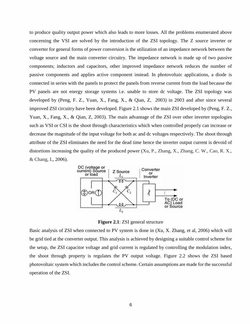
Figure 2.16: a) I-V waveform b) Experimental I-V waveforms
Even though Z source inverters have several advantages when compared to the traditional voltage or
source inverters, their applications in industry is limited. Conventional voltage or current source
inverters have much industrial application than Z source inverter. This limitation of the ZSI in industrial
application can be traced to but not limited to design layout, long frequency loop dc voltage bus
clamping which are investigated in (Cha, H., Li, Y., & Peng, F. Z., 2016) by adding clamping diode to
the circuit to reduce the frequency loop and circuit modification by intuition. So the useful solid structure
of the Z source inverter together with voltage clamping method for MCSI is simulated and experimental
results produce.

20
2.9 Trans and Quasi Topologies
The following procedures describe how the quasi Z source inverter is obtained from the basic impedance
network known as Z source inverter. Figure 2.17 shows the ZSI and Figure 2.18 shows the quasi Z
source inverter. These two inverter topologies are similar but with different passive component
arrangement. The qZSI is obtained from ZSI which is the foundation of all Z source topologies.
Capacitor C2 in Figure 2.17 shares the same ground with the source voltage which means that it can be
moved to the top of the source as in Figure 2.18. Once that is done, inductor L2 of Figure 2.17 is in series
with the source voltage so it can be arranged as in Figure 2.18. The position of L1 and L2 do not matter
because in the case of symmetry, the values of L1 and L2 are equal so is it the case of the capacitors. The
main advantage of qZSI over ZSI is the continuous input current from the source because inductor L1 is
connected in series to source voltage and the simple layout of the circuit. However the voltage gain and
the boost factor of ZSI and qZSI are equal and given by (2.33) and (2.34).
Figure 2.17: Z source inverter
Figure 2.18: q-Z source inverter
G = 𝑣�̂�𝑉𝑖𝑛2
= MB……………………………………………………………………………. (2.33)
B = 1
1−2𝐷𝑠ℎ ……………………………………………………………………………….. (2.34)
Theoretically the voltage gain capabilities of the ZSI and qZSI are infinite hence a smaller modulation
index is used when very high voltage gains are required. The smaller the modulation index, the higher

21
the stress developed across the inverter components (Qian, W., Peng, F. Z., & Cha, H., 2011). The Trans
ZSI was improved version of the qZSI to reduce the stress levels of the inverter and also increase the
boost factor. In the case of the inductors, single inductors or coupled inductors can be used and the turns
ratio is 1:1. The turns ratio when coupling is done between L1 and L2 is x:1 when capacitor C2 is taken
out of the circuit (Figure 2.19a) and the turns ratio changes to 1:x when C1 capacitor is removed. The
coupled inductor turns ratio is represented by x and the boost factor for the Trans Z source inverter is
given by:
B = 1
1−(1+𝑛)𝐷𝑠ℎ …………………………………………………………………………. (2.35)
Detailed analysis of the effects of stray inductance on the performance of the inverter is explained in
(Cha, H., Li, Y., & Peng, F. Z., 2016) and practical solutions given. This is mainly achieved by reducing
the loop area and loop length between the dc source and the inverter bridge. One method proposed is
application of two layer busbar lamination; this solves the problem caused by parasitic inductance or
stray inductance. Also the number of busbar is not limited on two since 5 busbar is applicable; the other
solution is the application of snubber circuits. In the improved Trans Z source inverter, a clamping diode
Dc is added to the circuit to reduce the loop length and also solve the effects of stray inductance.
Figure 2.19: Trans Z source inverter.

22
(a)
(b) (c)
Figure 2.20: a) Improved trans. ZSI b) Improved trans. ZSI and high frequency loop
c) high frequency loop in the improved trans. ZSI with the addition of clamp diode
(a) ∑ZSI
(b)Quasi ∑ZSI (c) Quasi ∑ZSI with Dc
Figure 2.21: ∑𝑍𝑆𝐼 𝑎𝑛𝑑 𝑄𝑢𝑎𝑠𝑖∑𝑆𝐼

23
(a)TZSI ([25] S. Jiang, D. Cao, and F. Z. Peng, 2011)
(b) Quasi TZSI (c) Quasi TZSI with Dc
Figure 2.22: TZSI and Quasi TZSI
An improvement in the basic structure of the Z source inverter was reported in (Shen, H., Zhang, B.,
Qiu, D., & Zhou, L.,2016) in which a common ground application was applied in Z source dc-dc
converter having very high voltage gain. The introduction of renewable energy sources into power
generation is an added advantage because of its positive attributes to the environment and relatively
cheap when compared to conventional power generation systems. Wind and photovoltaic systems are
the leaders in renewable energy system because of ease of installation and availability of smaller units
for residential applications; fuel cells are gradually becoming widely available.
For better and efficient utilization of renewable energy, a good power converter is required to efficiently
condition the power for standalone residential application or grid integration. Renewable energy source
power generation systems have a wide range of output power because of the unreliable nature of the
weather which is the ‘fuel’, hence a good power converter should be able to boost the output power
regardless of the input power. Previous applications make use of double stage power conversion because
a single converter does not have buck-boost capabilities.
2.10 Z Source dc-dc Converter
The conventional boost dc-dc converter has been applied widely for output power boosting and can
produce infinite voltage if the duty cycle of the converter is equivalent to one. However parasitic
resistance causes limitation on the peak level of the duty cycle. Theoretically the voltage gain of this
converter is infinite but in practical applications it’s limited (Li, W., & He, X..,2011; Wai, R. J., & Duan,
R. Y, 2005; Zhou, Y et al, 2003; Emadi,A. 2014 ). To overcome the limitations of this converter, several

24
topologies of converters have been proposed, examples are; non isolated boost dc-dc converter, non-
isolated with voltage multiplier technique (Prudente, M et al, 2008; Pfitscher, L. L et al, 2014, Axelrod,
B et al, 2003). Switched inductor topology (Axelrod, B et al, 2003, Tang, Y et al, 2015), switched
capacitor topology (Abutbul, O e al, 2003, Luo, F. L., & Ye, H., 2004; Wu, G et al, 2015, Liang, T. J et
al, 2012), cascaded topology (Walker, G. R., & Sernia, P. C., 2004).
The above so called improved topologies are too complex to operate also escalates the overall cost of
the system and the system volume is also enlarged, efficiency is also reduced. The Z source network can
overcome all the drawback of this converter and also render a high boosting ability with higher
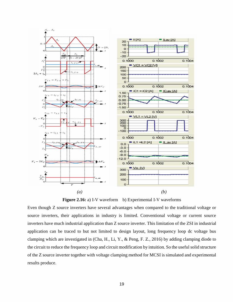
efficiency. An example of the impedance network coupled to a dc-dc converter (Zhang, J., & Ge, J.,
2010) is shown in Figure 2.23a whiles Figure 2.23b shows the novel version of the ZS dc-dc converter.
The difference between the topologies is that the diode in Figure 2.23a. is substituted to an inductor in
Figure 2.23b. Detailed explanations of the merits and demerits of various improved Z source topologies
have been presented in (Shen, H., Zhang, B., Qiu, D., & Zhou, L, 2016).
Figure 2.23: Z source dc-dc converter
The presented Z source dc-dc converter in (Shen, H et al, 2016) is shown in Figure 2.22, Figure 2.21a
and Figure 2.21b shows the circuit diagram of the modes of operations; ‘zero’ state and ‘one’ state. The
advantage of this dc-dc converter is the high voltage gain attributes and the common ground between
the input and output sections of the converter. Slight adjustment of the load location produce the
magnitude of the high voltage gain desired (Shen, H et al, 2016), other merits of the converter is the low
voltage stress on the components and simple layout of the converter. The application of this converter
can be in two folds; in single stage power conversion systems and double stage power conversion
systems like PV systems. The application of this topology in double stage conversion system will
produce highly efficient system and allow maximum power tracking (Xue, Y et al, 2004). The layout of
this topology is very and it is made up of the following passive components; two inductors L1and L2,
two capacitors C1 and C2, and two diodesD1 and D2, one switch S, a filtering capacitor C3 and the load
R. The difference between this topology and conventional converter in Figure 2.23a is the position of

25
the load and ground with respect to the source input, also the load and the source input are located on
the same section of the impedance network of the converter and share the ground.
Figure 2.24: Z source dc-dc converter
The principle of operating the Z source dc-dc converter is similar to other z source converters, the
symmetric conditions that exist in the basic Z source network applies to this topology as well, there’s a
linear increase and decrease of the capacitor voltage (vL1 and vL2) and inductor currents (iL1 and iL2).
Hence the following conditions are valid:
{𝑖𝐿 = 𝑖𝐿1 = 𝑖𝐿2, 𝑖𝐶 = 𝑖𝐶1 = 𝑖𝐶2
𝑣𝐿 = 𝑣𝐿1 = 𝑣𝐿2, 𝑣𝐶 = 𝑣𝐶1 = 𝑣𝐶2…………………………………….……….…... (2.36)
In state 0:
vL = vC = L𝑑𝑖𝐿
𝑑𝑡 ….……………………………………………..………………....…... (2.37)
Vo = vL + vC = L𝑑𝑖𝐿
𝑑𝑡 + vC ….……………………………………………………..…... (2.38)
iC = C𝑑𝑖𝐶
𝑑𝑡 ≈ iL + Io ….……………………………………………………..……..….... (2.39)
In state 1:
Vi = vL + vL = L𝑑𝑖𝐿
𝑑𝑡 + vC….………………………………………………………….... (2.40)
ii = iC + iL = C𝑑𝑣𝐶
𝑑𝑡 + iL ………….……………………………………………………. (2.41)
The continuous conduction mode of the converter can be categorized into two modes of operation; 0
states and 1 states. Figure 2.26 show waveform output for these modes of operation. These modes of
operation occur in the dynamic state. The zero state is shown in Figure 2.26a while the one state or state
one is shown by Figure 2.26b.
26
Figure 2.25: Z source dc-dc converter
Figure 2.26: Sate one and zero waveform.
Table 2.1: Current of each Component in Different States

27
Table 2.2: Comparison on Number of Component
Table 2.3: Comparison of Switch Stress

28
Table 2.4: Comparison of Diode Stress
Figure 2.27: Comparison of Voltage gains
A resonant Z source converter (González-Santini, N. S et al, 2016) with power factor correction is
applied in wireless power transfer applications such as the charging of electric vehicle batteries. The Z
source resonant converter executes output voltage regulation and power factor correction simultaneously
due to impedance network in the structure of the converter. Three different on board battery charging
converter is presented and compared with proposed topology. A simplified diagram of electric vehicle
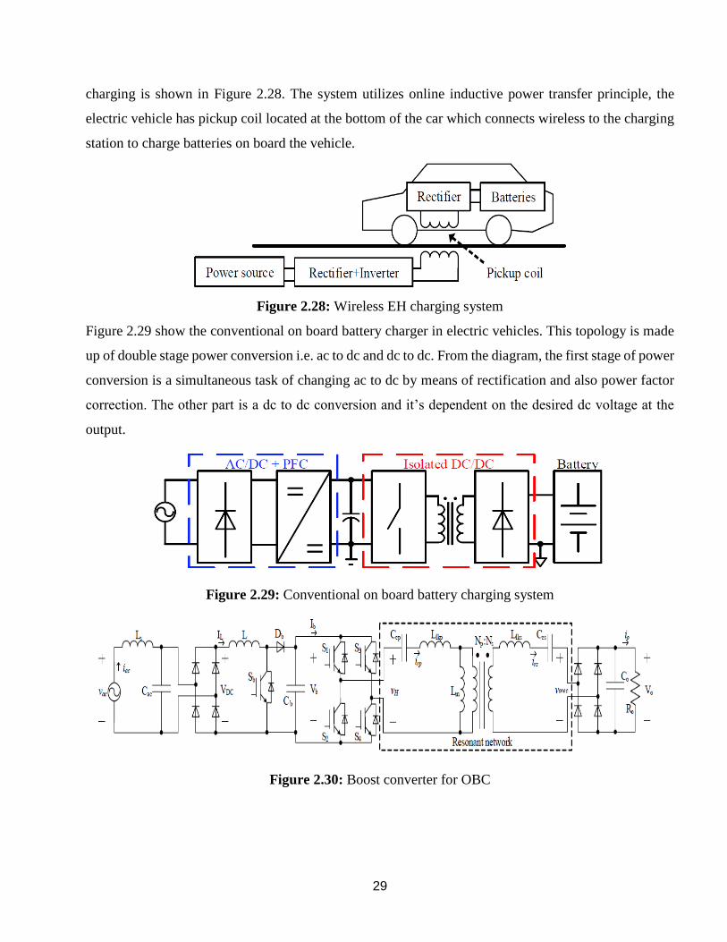
29
charging is shown in Figure 2.28. The system utilizes online inductive power transfer principle, the
electric vehicle has pickup coil located at the bottom of the car which connects wireless to the charging
station to charge batteries on board the vehicle.
Figure 2.28: Wireless EH charging system
Figure 2.29 show the conventional on board battery charger in electric vehicles. This topology is made
up of double stage power conversion i.e. ac to dc and dc to dc. From the diagram, the first stage of power
conversion is a simultaneous task of changing ac to dc by means of rectification and also power factor
correction. The other part is a dc to dc conversion and it’s dependent on the desired dc voltage at the
output.
Figure 2.29: Conventional on board battery charging system
Figure 2.30: Boost converter for OBC

30
Figure 2.31: Proposed Z source resonant converter
The advantages of the traditional boost converter for on board battery charger are; low cost of the
converter, power factor and power density are high, has good efficiency (Musavi, F et al, 2012). This
topology is not suitable for high power applications the efficiency decreases due to the high losses
incurred at the rectifier stage hence powers up to 3.5kW are suitable range for applications (Musavi, F
et, 2012, Yilmaz, M., & Krein, P. T., 2013). The proposed topology has fewer semiconductor switches
when compared to the boost topology but the proposed topology also has more passive components than
the boost topology. The size and weight of the boost topology will be much higher due to the heat sink.
There are three modes of operation state for the proposed Z source resonant converter as depicted in
Figure 2.32. And the corresponding output waveforms are shown in Figure 2.33
a) Active state
b) Shoot through state
c) Traditional zero state
Figure 2.32: Modes of operation of ZSRC

31
Figure 2.33: Modes of operation output waveforms
This paper (Dong, S., Zhang, Q., & Cheng, S., 2015) analysis the effects of ripples produced by the
capacitor voltage and the critical inductance on bidirectional Z source inverter. Different literature areas
(topology, parameters of the design, PWM control techniques) of Z source converter have been
published over the and suitable application areas such as renewable energy sources; PV systems, wind
energy, hybrid electric vehicles, power factor correction, motor speed control have been noted (Peng, F
e al, 2007 , Lei, Q et al, 2014). Although Z source inverters have several advantages, there are a few
draw backs such as large area required by capacitor and inductor which increase the overall space of the
system. Conventional ZSI operates in two modes; continuous conduction mode CCM or discontinuous
conduction mode DCM but that’s not the case of the bidirectional Z source inverter shown in Figure
2.34. B-ZSI operates in CCM only because the bidirectional switch Sw7 enables reverse current flow
from the load to the source. This paper categorizes the conduction modes of the bidirectional ZSI into
the following groups:
[1] Complete Inductor Energy-supplying Mode (CIEM)
[2] Incomplete Inductor Energy-supplying Mode (IIEM)
[3] Zero-crossing Input Current Mode (ZPCM)
[4] Non-zero-crossing Input Current Mode (NPCM)
[5] Zero-crossing Inductor Current Mode (ZICM)
[6] Non-zero-crossing Inductor Current Mode (NICM)

32
Figure 2.34: B-ZSI
Two modes (NICM and ZICM) of operation of Z source inverters exist; this is as results of the fact that
the current of the inductor intersect the zero point or not. There are two groups of NICM mode of
operation; CIEM and IIEM and their waveforms of the inductor current and capacitor voltage are shown
in Figure 2.35 a and b respectively. The indictor current and capacitor voltage for the other mode of
operation ZICM is shown in Figure 2.36.
Figure 2.35: NICM of B-ZSI. (a) CIEM. (b) IIEM.

33
Figure 2.36: ZICM of B-ZSI
2.11 QZSI Based 1ph to 3ph
Several quasi Z source topology and applications have been presented since the four different quasi
impedance topologies were presented in 2008 (Anderson, J., & Peng, F. Z., 2008). The first publication
based application of qZSI is in photovoltaic energy generation system (Cintron-Rivera et al, 2009).
Subsequently other forms of application have been published. In (Khosravi, N. A. e al, 2014), a qZSI
topology is presented with reduced number of components and also three phase system is derived from
a single phase inverter. The circuit of the proposed inverter is composed of four switches (H Bridge)
and two capacitors in series with a neutral point in them. Figure.37 shows the circuit structure of the
proposed inverter. The following advantages makes the HBqZSI more suitable for practical applications
than the conventional ZSI; four switches means reduced switching losses, THD content is minimized,
cost of the system is reduced because of less component usage. The application of space vector PWM
translates into quality dc link voltage into the main converter circuitry hence filter cost and losses are
eliminated. The structure of Figure 2.33 is made up of quasi impedance block, the H bridge block
together series chain capacitors, three phase load and an LC filter block. The load is a resistive connected
in wye connection. This topology is also suitable for 3-ph induction motor applications.
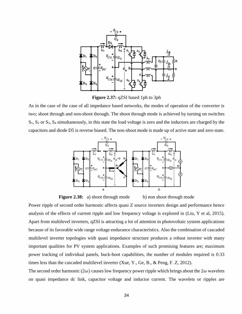
34
Figure 2.37: qZSI based 1ph to 3ph
As in the case of the case of all impedance based networks, the modes of operation of the converter is
two; shoot through and non-shoot through. The shoot through mode is achieved by turning on switches
S1, S2 or S3, S4 simultaneously, in this state the load voltage is zero and the inductors are charged by the
capacitors and diode D5 is reverse biased. The non-shoot mode is made up of active state and zero state.
Figure 2.38: a) shoot through mode b) non shoot through mode
Power ripple of second order harmonic affects quasi Z source inverters design and performance hence
analysis of the effects of current ripple and low frequency voltage is explored in (Liu, Y et al, 2015).
Apart from multilevel inverters, qZSI is attracting a lot of attention in photovoltaic system applications
because of its favorable wide range voltage endurance characteristics. Also the combination of cascaded
multilevel inverter topologies with quasi impedance structure produces a robust inverter with many
important qualities for PV system applications. Examples of such promising features are; maximum
power tracking of individual panels, buck-boot capabilities, the number of modules required is 0.33
times less than the cascaded multilevel inverter (Xue, Y., Ge, B., & Peng, F. Z, 2012).
The second order harmonic (2𝜔) causes low frequency power ripple which brings about the 2𝜔 wavelets
on quasi impedance dc link, capacitor voltage and inductor current. The wavelets or ripples are

35
detrimental to smooth design and operation of qZSI hence they must be reduced to an acceptable range.
As at the time of the publication of (Liu, Y et al, 2015) no literature has been published to investigate
the effects of second order harmonic on qZSI. In the case of multilevel inverters, several publications
have been made which address the concern of 2𝜔 and three phase qZSI analysis has been done to curtail
the effects second order effects on inductor current, dc link and capacitor voltage. (Liu, Y et al, 2015;
Xue, Y et al, 2012; Xue, Y et al, 2011; et al, 2014; Rajakaruna, S., & Jayawickrama, L., 2010). The
circuit structure is similar to all qZSI but with PV as source input.
A similar topology of qZSI is proposed to investigate the effects of the second order harmonics on
systems design and performance. In this topology the qZSI has energy storage device (battery)
connected in parallel to the capacitor. The main analysis of this paper (Liang, W et al, 2018) is to add a
battery to topology and also use asymmetrical impedance components to see the effects on the system
size which is a good parameter for an efficient converter. The asymmetrical quasi impedance based
inverter has the ability to reduce the volume, size and eventually the cost and most importantly maximize
the power density of the system (Liang, Z et al, 2015; . Hu, Z. Liang, and X. He, 2016; S. Hu, Z. Liang,
D. Fan, and X. He, 2016).
2.12 QZSI and T type Inverter
A quasi Z source inverter combined with T type multilevel inverter is proposed in (Pires, V. F et al,
2016) and its operations investigated under two modes; normal operating condition and fault operating
conditions. Application of the conventional 3-ph 2-level converter is enormous in industry due to its
simple structure and ease of control, low cost and very high efficiency but there are some demerits which
hinders the optimum operation of this converter; only buck capabilities unless boost converter is added
to the structure, dead time or short circuit. The ZSI topology overcomes all this disadvantages [Abu-
Rub, H et al, 2013; Battiston, A et al, 2014; T.-W. Chun, E.-C. Nho, 2015; Pires, V. F et al, 2014 Guo,
F., et al., 2013; Husev, O et al, 2015).
The qZSI, which is an improvement of the conventional ZSI topology, provides the following attributes;
continuous input current from the source, wide range of voltage applications and reduced ratings of
components. Also the combination of qZSI and other multilevel inverters is not successful but able to
retain the advantages of the two topologies hence several publications has been made about multilevel
inverter based qZSI (Ott, S et al, 2011). The presented topology of (Abu-Rub, H et al, 2013) is shown
in Figure 2.39.

36
Figure 2.39: qZSI + T type inverter
The circuit of qZSI + T type inverter is made up of two quasi impedance network connected to a two
series chain capacitor with a neutral point between the capacitor connection, a T type composed of
bidirectional and unidirectional is connected an RL load. The number of bidirectional switch is 3 and 6
unidirectional switches for H Bridge. Two modes of operations exist; shoot through and non-shoot
through. Five levels of voltage can be produced at the inverter and their magnitude is dependent on the
boost factor. Two conditions of fault are critical for the components in the converter i.e. open circuit and
short circuit. The short circuit fault is already protected by the impedance network so the open circuit
fault was investigated by (Abu-Rub, H et al, 2013). An open circuit fault in any of the lower or upper
legs leads to a new arrangement of the circuit to produce a new topology. For example if there should
be a fault in phase A in Figure 2.39, its corresponding configuration is shown in Figure 2.40. The new
topology is derived by precluding all switches on that leg (phase A) turning on its corresponding
bidirectional switch (S2), also the modulation methodology will change. Figure 2.41 show the new
arrangement or topology if the open circuit fault occurs in any of the bidirectional switches which links
the impedance network to the T type inverter. In this specific example, the bidirectional switch S2 is
disabled due to open circuit fault. The change in the modulation strategy is not as huge as in the open
circuit fault of a phase leg.
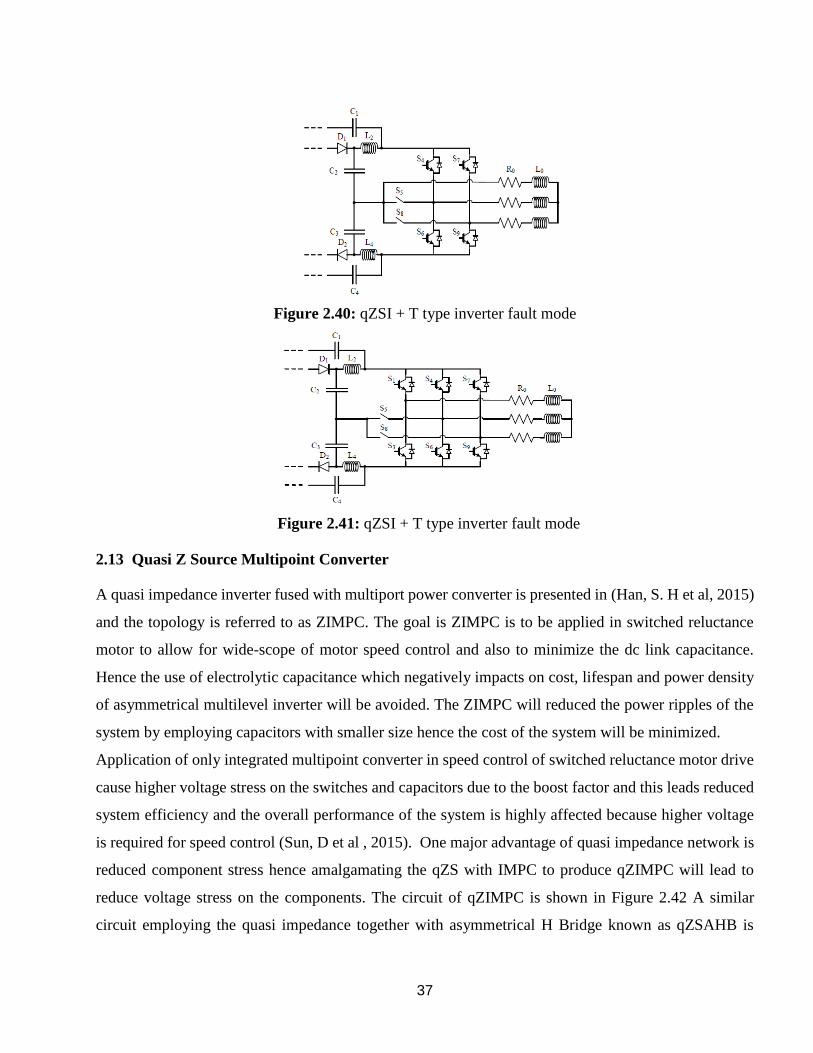
37
Figure 2.40: qZSI + T type inverter fault mode
Figure 2.41: qZSI + T type inverter fault mode
2.13 Quasi Z Source Multipoint Converter
A quasi impedance inverter fused with multiport power converter is presented in (Han, S. H et al, 2015)
and the topology is referred to as ZIMPC. The goal is ZIMPC is to be applied in switched reluctance
motor to allow for wide-scope of motor speed control and also to minimize the dc link capacitance.
Hence the use of electrolytic capacitance which negatively impacts on cost, lifespan and power density
of asymmetrical multilevel inverter will be avoided. The ZIMPC will reduced the power ripples of the
system by employing capacitors with smaller size hence the cost of the system will be minimized.
Application of only integrated multipoint converter in speed control of switched reluctance motor drive
cause higher voltage stress on the switches and capacitors due to the boost factor and this leads reduced
system efficiency and the overall performance of the system is highly affected because higher voltage
is required for speed control (Sun, D et al , 2015). One major advantage of quasi impedance network is
reduced component stress hence amalgamating the qZS with IMPC to produce qZIMPC will lead to
reduce voltage stress on the components. The circuit of qZIMPC is shown in Figure 2.42 A similar
circuit employing the quasi impedance together with asymmetrical H Bridge known as qZSAHB is

38
shown in Figure 2.43. The circuit in Figure 2.42 requires extra leg to provide the shoot through mode.
Figure 2.42: qZIMPC
Figure 2.43: qZSAHB
Compared to asymmetrical H bridge topology the proposed qZIMPC has the following advantages
which are summarized in Table 2.5;
1. The dc source voltage is not modified by the capacitor voltage because the two are not linked
together.
2. The magnitude of the capacitors ripple voltage and average voltage should be high as possible in
other to minimize the capacitance value to the least feasible level.
3. Electrolytic capacitor is eliminated because the source current is filtered by an inductor.
4. The impedance source provides an easily changeable dc link voltage which useful in the speed
control of the switched reluctance motor.
5. The component count is minimized which directly translates to reduced cost and improved power
density.
Table 2.5: Comparison between Proposed ZIMPC and conventional ASHB Topology

39
2.14 qSBZS+T-type
Quasi switched boost topologies are further improvements on the quasi impedance source inverter to
basically maximize the boost factor as much as possible. A quasi switched boost T type inverter is
presented in (Nguyen, M. K et al, 2016), its pulsewidth control methods, analysis verification of the
inverter are investigated. The voltage output level of the proposed inverter is 3. In other to reduce the
current ripples, novel PWM control technique is proposed. The proposed control technique, the duty
cycle of the shoot through mod is kept constant and the duty cycles (of the switches) are varied, this
helps to maintain a very high modulation index. The circuit of the proposed qSBZS+T-type is shown in
Figure 2.44. Figure 2.45 shows the various states of operation of the inverter; shoot through and noon-
shoot through. There are four modes (Figure 2.45a to Figure 2.45d) of non-shoot through which
represents the active states of the switches and one shoot through mode; Figure 2.45e.
Figure 2.44: qSBZS+T-type

40
Figure 2.45: Modes of operation of qSBZS+T-type
The circuit of Figure 2.44 is derived by adding an impedance network which is made up of two switches,
four diodes, two capacitors and an inductor (which connected in series to the dc source) to traditional
the three-level T type inverter. This methodology is helps in boosting the output ac voltage and the
inductor provides continuous current input from the source. The mode of operation is summarized into
table 2.6 and its corresponding boost factor is given by (2.42). Comparison of the proposed invert to
other similar topologies is presented in Table 2.7
B = 2𝑀
4−6𝐷𝑜−𝑑1−𝑑2 …………………………………………………………………… (2.41)
Table 2.6: Switching States of the Proposed QSBT2I (x=a, b, c)

41
Table 2.7: Comparison of the three – level QSBT2I with other impedance – source – based three level
inverter
2.15 Quasi Switched Boost Cascaded HB Inverter
A cascaded H-bridge topology is improved by the addition of quasi switched boost impedance network.
As stated above the quasi switched boost is an improvement over the quasi Z source network having the
following merits; reduced component number and higher boost factor. In (Bratcu, A. I et al, 2011) the
quasi switched boost impedance structure is combined with H Bridge inverter to produce 5 level
qSBCHBI. This topology combines the advantages of the cascaded H Bridge inverter (quality output
waveform, reduced harmonic content, reduced filter component ratings and good resistant to the effects
of EMIs) and the quasi impedance network. The topology of qSBCHBI is shown in Figure 2.46.
Figure 2.46: qSBCHBI
The proposed qSBCHBI is made up of two modules of H Bridge connected in series. Each module has

42
dc voltage source quasi switched boost impedance network connected to it. The impedance network is
made up of one switch, one inductor, one capacitor and two diodes. The output voltage of qSBCHBI is
the addition of the output voltages of the modules; Vo1 and Vo2 as shown in Figure 2.46. Table 1
compares two cascaded quasi Z source topologies. From the table 2.8, it is evident that the proposed
topology has reduced component count hence the cost of the system is decreased but the switching loses
is increased because two more switches are employed in qSBCHBI. Higher levels of output voltage will
reduced the system size.
Table 2.8 : Comparison between cascaded five – level qSBI and qZSI
Cascaded qSBI Cascaded qZSI
number of inductors 2 4
number of capacitors 2 4
number of diodes 12 10
number of switch 10 8
Just as in the case all impedance source structures, two modes of operations exist; shoot through mode
and non-shoot through mode. Figure 2.47a and 2.47b shows these two modes respectively. In the shoot
through mode switch So is gated on and the two diodes Da and Db are reverse biased. The inductor is
charged by the capacitor and the dc link voltage VPN is zero. In the non-shoot through mode switch So
is opened and diodes Da and Db are forward biased, the inverter circuit power is supplied by the inductor
and it functions as a current source. (2.42) and (2.43) give the KVL for the two modes respectively. The
voltage output level of this proposed inverter is not limited to 5 but can be extended to a much higher
levels as desired. In multilevel inverters, high levels of output voltage correspond to much higher quality
output waveforms.
(a) (b)
Figure 2.47: a) Shoot through b) Non-shoot through
VL =L 𝑑𝑖𝐿
𝑑𝑡 = 𝑉𝑑𝑐 + 𝑉𝐶……………………………………………………………….. (2.42)

43
{𝑉𝐿 = 𝑉𝑑𝑐 − 𝑉𝑐𝑉𝑐 = 𝑉𝑃𝑁
…………………………………………………………….………….. (2.43)
2.16 Quasi switched Boost dc-dc Converter
An isolated high boost quasi switched boost inverter is presented in (Wu, G., et al, 2015). This topology
has the following merits; the source current is continuous, the system is definitive because its operation
in open and short circuits are not restricted, the isolation transformer has minimized turns ratio, variable
shoot through duty cycle does not change the voltage waveforms of the secondary and primary windings.
Isolated and non-isolated converters have received much attention in recent years in areas of higher
boosting capabilities. Galvanic seclusion is not present in non-isolated converters hence the following
methods have been provided: cascaded topologies, switched capacitor, coupled inductor, voltage
multiplier units, switched inductor to function in transformer less systems to provide high boost and
maximum power density and efficiency (ang, Y et al, 2015 , Nymand, M., & Andersen, M. A,2010).
Isolated converters were proposed to address the drawbacks in the no-isolated topologies; these
drawbacks are mainly about safety standards (Wu, G et al, 2015). Step-up converters combined with
transformers and voltage lift methodologies are some examples of isolated converters (LaBella, T., &
Lai, J. S, 2014 , Nguyen, M. K et al, 2018).
The proposed high step-up quasi switch boost dc to dc converter is shown in Figure 2.48. The circuit is
composed of quasi switched boost inverter, voltage double rectifier and isolation transformer. The
impedance network is made up of two diodes, one inductor and capacitor each, the inverter circuit has
four semiconductor switches with four anti-parallel diodes, one step-up seclusion transformer and the
voltage double rectifier has two capacitors and two diodes. The modes of operations are continuous
conduction mode and discontinuous conduction mode. Also shoot through and non-shoot through modes
exist.
Figure 2.48: Quasi switched boost dc-dc converter
2.17 SC/qSBI
Combinations of two switched topologies are presented in (Ahmed, H. F et al, 2016) the switched
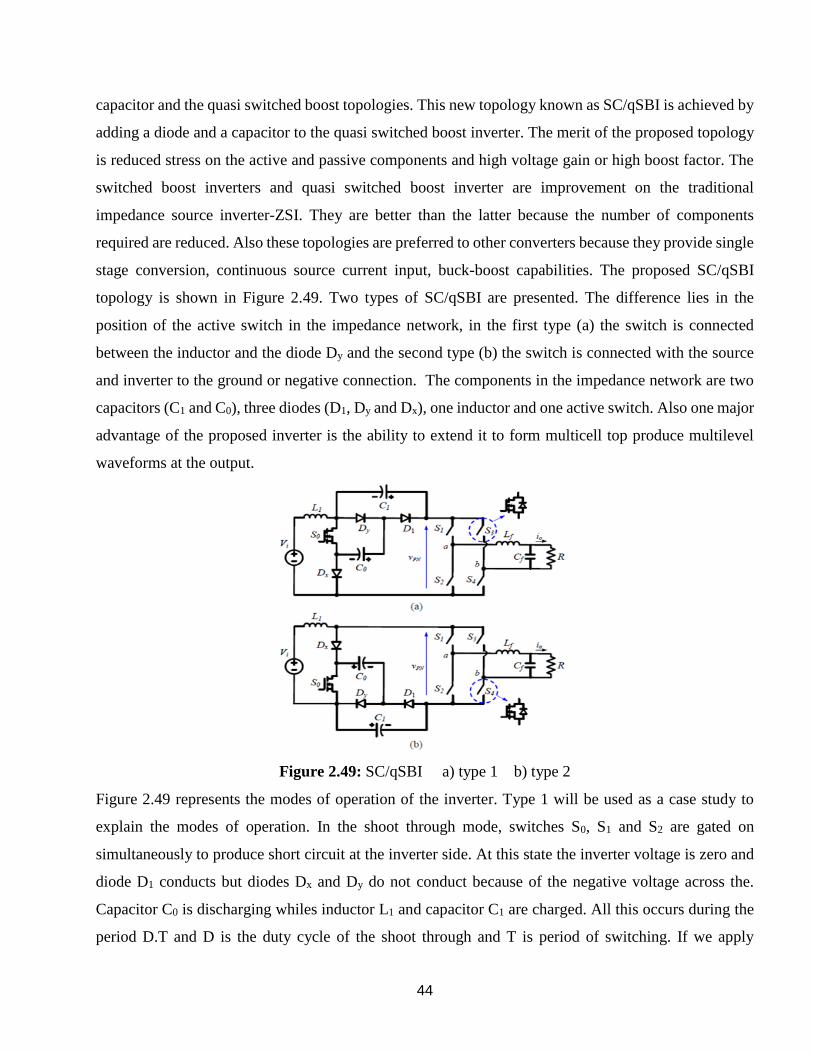
44
capacitor and the quasi switched boost topologies. This new topology known as SC/qSBI is achieved by
adding a diode and a capacitor to the quasi switched boost inverter. The merit of the proposed topology
is reduced stress on the active and passive components and high voltage gain or high boost factor. The
switched boost inverters and quasi switched boost inverter are improvement on the traditional
impedance source inverter-ZSI. They are better than the latter because the number of components
required are reduced. Also these topologies are preferred to other converters because they provide single
stage conversion, continuous source current input, buck-boost capabilities. The proposed SC/qSBI
topology is shown in Figure 2.49. Two types of SC/qSBI are presented. The difference lies in the
position of the active switch in the impedance network, in the first type (a) the switch is connected
between the inductor and the diode Dy and the second type (b) the switch is connected with the source
and inverter to the ground or negative connection. The components in the impedance network are two
capacitors (C1 and C0), three diodes (D1, Dy and Dx), one inductor and one active switch. Also one major
advantage of the proposed inverter is the ability to extend it to form multicell top produce multilevel
waveforms at the output.
Figure 2.49: SC/qSBI a) type 1 b) type 2
Figure 2.49 represents the modes of operation of the inverter. Type 1 will be used as a case study to
explain the modes of operation. In the shoot through mode, switches S0, S1 and S2 are gated on
simultaneously to produce short circuit at the inverter side. At this state the inverter voltage is zero and
diode D1 conducts but diodes Dx and Dy do not conduct because of the negative voltage across the.
Capacitor C0 is discharging whiles inductor L1 and capacitor C1 are charged. All this occurs during the
period D.T and D is the duty cycle of the shoot through and T is period of switching. If we apply

45
KVL/KCL to Figure 2.50a, the following mathematical expressions will be produced:
{
𝑉𝐿1 = 𝑉𝑖 + 𝑉𝐶𝑂𝑉𝐶𝑂 = 𝑉𝐶1𝑉𝑃𝑁 = 0
…………………………………………………….…………………… (2.44)
{𝑖𝑐0 = −𝑖𝐶1𝑆𝑇 − 𝐼𝐿1
𝑖𝐶1 = 𝑖𝐶1𝑆𝑇………….……………………………………………………….…. (2.45)
Figure 2.50b represents the non-shoot through mode of the inverter, switch S0 is turned off and the
inverter operation is the same conventional modes of operation; active states and zero state. Diode D1 is
now non-conducting while’s diodes Dx and Dy are conducting. Capacitor C0 is fully charged and
capacitor C1 and inductor L1 are discharged. If we apply KVL/KCL to Figure 2.50a, the following
mathematical expressions will be produced:
{𝑉𝐿1 = 𝑉𝑖 − 𝑉𝐶0𝑉𝑃𝑁 = 𝑉𝐶0 + 𝑉𝐶1
………………………….……………………………………..…….. (2.46)
{𝑖𝐶0 = 𝐼𝐿1 − 𝐼𝑃𝑁𝑖𝐶1 = −𝐼𝑃𝑁
…………………………………………………………….………….. (2.48)
The boost factor of the proposed switched capacitor – quasi switched boost inverter is twice that of the
quasi boost inverter and is given in (2.49).
B = 2
1−2𝐷 …………………………………………………………………………………. (2.49)
Figure 2.50: Operational states of SC/qSBI
The multi cell structure of the proposed switched capacitor – quasi switched boost inverter is shown in
Figure 2.51 and the boost factor is represented in two forms i.e. when n is odd or even.

46
Figure 2.51: Multicell structure of SC/qSBI
Boost factor B =
{
2+𝑖𝑛 (
𝑛
2)
1− [2+𝑖𝑛 (𝑛
2)]𝐷 𝑛 = 𝑜𝑑𝑑 𝑛𝑢𝑚𝑏𝑒𝑟
1+𝑛
2
1−(2+𝑛
2)𝐷 𝑛 = 𝑒𝑣𝑒𝑛 𝑢𝑚𝑏𝑒𝑟
………………………………………….………. (2.50)
2.18 SCL/qZSI
The switched capacitor/coupled inductor quasi Z source topology (Peng, F. Z., Shen, M., & Qian, Z.,
2005) is derived by combining three other impedance sourced topologies: the switched capacitor, the
switched couple inductor with three windings and the quasi Z source inverter.
This new topology is referred to as SCL/qZSI and it possess all the advantages of three topologies;
reduced voltage stress on the active and passive components. Higher boost factor, immunity to the
effects EMI, continuous input current, reduced component count, the applied modulation index is hence
quality output waveforms are produced, inrush current at startup is reduced, common node for the source
voltage. in the inverter circuit (Shen, M., et al, 2006 , Adda, R et al, 2013). The proposed SCL/qZSI is
shown in Figure 2.52. The circuit is made up of the impedance network which is composed of the
switched capacitor, switched coupled inductor and the quasi impedance network and the three phase H
bridge circuit made up of six switches. The impedance structure has one inductor, three windings of
coupled inductor, two capacitors, three diodes. The modes of operations are shoot through state and the
non-shoot through state which are shown in Figure 2.53a and 53b respectively.

47
Figure 2.52: SCL/qZSI
Figure 2.53: a) Shoot through b) non-shoot through
In the shoot through state diode Din is reversed biased and diode D1 and D2 are forward biased, capacitor
C1 charges windings N1 and N2, also C1 charges capacitor 3 via windings N3. In the non-shoot through
state, diode Din is forward biased and diode D1 and D2 are reverse biased. Power to the inverter circuit
is provided capacitor C3 and the three windings. Applying KVL/KCL to Figure 2.53a and 53b will
produce (2.51) and (2.52) respectively.
{
𝑉𝐿1 = 𝑉𝑖𝑛 + 𝑉𝐶2𝑉𝑁1 = 𝑉𝐶1, 𝑉𝑁3 = 𝑛𝑉𝑁1𝑉𝐶3 = (𝑛 + 1)𝑉𝐶1
………………………………………….………………….. (2.51)
{
𝑉𝐿1 = 𝑉𝑃𝑁 − 𝑉𝑖𝑛 − 𝑉𝐶2𝑉𝐶2 − 𝑉𝐶3 = 𝑉𝑁1 + 𝑉𝑁2 + 𝑉𝑁3
𝑉𝑁1 + 𝑉𝑁2 + 𝑉𝑁3 = 𝑉𝑃𝑁 − 𝑉𝐶1 − 𝑉𝐶3
………………………………………………….. (2.52)
The boost is given by (2.53) where n is the turns ratio of the windings
B = 𝑛+2
(1−(3+𝑛)𝐷) ……………………………………………………………..…………….. (2.53)

48
Table 2.9: Comparison of selected transformer type impedance source inverters
Topology TSI-TZSI Y- ZS ΣZSI ITQSZI AгZSI LCCTZSI TQZSI г ZSI TransAZSI
Component count 1-T
1-C
1-D
1-3wT
1-C
1-D
2-T
2-C
1-D
1-T
1-L
2-C
1-D
1-T
1-L
2-C
1-D
1-T
1_L
2-C
1-D
2-T
1-D
2-C
1-T
1-C
1-D
1-T
1-C
1-D
C.I.C No No No Yes Yes Yes Yes No Yes
Inrush current Yes Yes Yes No No No No Yes Yes
Common ground Yes Yes No Yes Yes Yes Yes Yes Yes
Boost Factor (1/1 – (n+1)D0) (1/1 – kD0) (1/1 - ɤD0) (1/1 (n + 2)D0) [1/1 (2 + (1/ɤгz
))D0]
(1/1 – (n + 1)D0) (1/1 – (n1 + n2
+2)D0)
[1/1 – (1 +
(1/гɤz –
1))D0]
(1/1 – (n + 1)
D0)
Footnotes:
1-T: one transformer
1-3wT: one transformer with 3 windings
2-C: two capacitors
1-D: one diode

49
2.19 Conclusion
The goal of this chapter of my thesis is a review of Z source inverter topologies or structures taken into
considerations the type of topology, mathematical analysis, its application in either industry or academia.
This review has exposed to me the qualities of Z source inverter such high boost functionality, single
stage voltage conversion, shoot through capabilities which protects the inverter from the negative
effectives EMIs. The Z source inverter employs an impedance network between the source and the main
inverter circuit to produce high boost or increase the voltage gain which absent in the conventional voltage
or current source inverters. Also voltage source converters are applicable in dc-ac inversion, dc-dc
conversion, ac-dc rectification and ac-ac conversion.

50
CHAPTER 3
POWER CIRCUIT DESCRIPTION AND SIMULATION RESULTS
3.1 Introduction
The process of changing dc voltage/power to ac voltage/power is known as inversion; this process is
realized by the use of principal device called an inverter. The first inverter is commonly known as the
conventional 2-level inverter which is a voltage source inverter- VSI. The voltage source inverter also
known as voltage source converter (when used for both inversion and rectifying purposes) has wide areas
of applications but it’s fraught with many limitations: a. it’s a buck or step down inverter that’s the output
voltage is always less than the input voltage unless a buck-boost converter is applied. When used as a
rectifier, it’s a boost rectifier circuit, b. applications of buck-boost converter in VSI topology increases
the cost of the unit, reduces the efficiency of the system and complicated control technique is introduced,
shoot through property is absent in VSI or CSI hence EMIs immunity is absent, inductor – capacitor filter
is required to reduce power systems noises. The introduction of conventional Z source inverter solved the
limitations of VSI and CSI, ZSI also has a number of limitation such as limited boosting capabilities and
high number of passive components as well as limited control of the impedance structure due to lack
active components.
3.2 Chosen Topology
The circuit impedance source topology is known as switched boost inverter (SBI); its circuit is shown in
Figure 3.1. The circuit of switched boost inverter is composed of passive and active components as the
impedance network sandwiched between the dc source and the single phase inverter bridge. The active
components are two diodes and a switch, whiles one inductor and one capacitor constitute the passive
components. The output of the H Bridge inverter is connected with an inductor-capacitor (LC) filter to
minimize the harmonic content in the output voltage.
Figure 3.2.1: Switched boost inverter

51
The circuit analysis of the switched boost inverter is similar to the traditional impedance source network;
shoot through analysis and non-shoot through analysis. In the shoot through mode, switch Gs is gated on
and this results in diodes Db and Da being turned off because the capacitor voltage is greater than the
source/input voltage, at this state the inductor is charged by the capacitor and the discharging current from
the capacitor equals to the inductor current. The duration of this process is D.Ts during switching period
of Ts. The circuit of the shoot through mode is shown if Figure 3.2a. The shoot through mode is achieved
by turning on simultaneously all switches on the same leg; this renders the inverter bridge short circuited
and hence the input voltage vi to the inverter bridge which is the output voltage from the impedance
network is zero. The non-shoot through mode is shown in Figure 3.2b and this occurs during the switching
period of Ts (1 – D); in this mode, the switch Gs is switched off. The input voltage to the bridge circuit
is supplied by the main source Vg and the inductor vL, also the capacitor is charged by these two voltages
(Vg and vL). The two diodes Da and Db are forward biased. Due to the inductor in series with the main
voltage source, the input to the inverter bridge is now a current source hence the inverter bridge becomes
current source inverter. The inverter input current Ii is the difference between the inductor current and the
capacitor current. Figure 3.3 show the equivalent switched boots inverter circuit in its simplified form.
Figure 3.2.2: a) shoot through b) non-shoot through
Figure 3.2.3: Clarified switch boost inverter circuit.

52
(a) (b)
Figure 3.2.4: a) SBI stable state waveforms b) SBI duty ratio
Using the stable state waveform analysis of Figure 3.4a, the following mathematical equations are derived
for the shoot through and non-shoot through modes. The inductor voltage, capacitor current and the
inverter bridge voltage are given by vL, iC, and vi respectively.
vL = vC, 0 < t < D.Ts and vL = Vg – vC, D.Ts < t < Ts (3.3)
iC = -iL, 0 < t < D.Ts and iC = iL – ii, D.Ts < t < Ts (3.4)
vi = 0, 0 < t < D.Ts and vi = vC, D.Ts < t < Ts (3.5)
The following equations (3.6) to (3.8) are derived from the above equations after applying small ripple
estimation.
vL = VC, 0 < t < D.Ts and vL = Vg – VC, D.Ts < t < Ts (3.6)
iC = -IL, 0 < t < D.Ts and iC = IL – Ii, D.Ts < t < Ts (3.7)
vi = 0, 0 < t < D.Ts and vi = VC, D.Ts < t < Ts (3.8)
The inverter bridge input voltage Vi which is known as the dc link voltage is determined by (3,9) and its
derived after applying charge second balance rule:
Vi = VC (1 – D) (3.9)
To determine the passive component values, KCL (Kirchhoff’s current law) and KVL (Kirchhoff’s voltage law)
can be applied to Fig. 3a and 3b, to derive the equations below. When switch S is closed, diodes Da and Db are
reverse biased because VC is greater VL and also the SBI is in the shoot through state hence they are in no-
conduction mode but when switch S is opened (non-shoot through state), diodes Da and Db are forward biased
hence they are in conduction mode. The inductor voltage VL equals to the capacitor voltage VC and the inductor
voltage is given by:
VL = VC (3.11)
Generally, the voltage across an inductor is given by

53
VL = L𝑑𝑖𝐿
𝑑𝑡 (3.12)
Hence the inductor current iL is given by
iL = 𝑉𝐶
𝐿t + ILV (3.13)
When the voltage across switch S is zero, the following mathematical equations are valid:
VS = 0
iS = iL = 𝑉𝐶
𝐿t + ILV (3.14)
The voltage across diodes D1 and D2 are given by:
VD1 = Vi – VC (3.15)
VD2 = -VC (3.16)
iD1 = iD2 = 0 (3.17)
When the voltage between the switched boost network and H-bridge is zero
Vdc = 0 (3.18)
idc = iS = iL = 𝑉𝐶
𝐿t + ILV (3.19)
Then the capacitor current becomes:
iC = -iL = - 𝑉𝐶
𝐿t - ILV (3.20)
When the voltage across switch S is not zero, the following mathematical equations are valid:
VS = VC - Vi (3.21)
Then the current across the switch becomes zero.
iS = 0 (3.22)
VD1 = VD2 = 0 (3.23)
iD1 = iL = 𝑉𝑖− 𝑉𝐶
𝐿t + ILP (3.24)
For state 1, idc equals to the current across the low pass filter inductor and for state 2, idc equals to zero,
however the capacitor current is given by:
iC = iD2 = iL – idc = 𝑉𝑖− 𝑉𝐶
𝐿t + ILP – iLf for state 1, (3.25)
For state 2, iC = iD2 = iL – idc = 𝑉𝑖− 𝑉𝐶
𝐿t + ILP (3.26)

54
3.3 Conclusion
Analysis and simulation of the proposed impedance source inverter known as Switched Boost Inverter
has been investigated in this chapter. The mathematical analysis of the inverter to determine various
components ratings has been done, also the two modes of operations of the Z source topologies has been
verified. Two techniques (conventional PWM and Modified PWM) for inverter control was applied for
simulation and the results generated in Figure 3.5 to Figure 3.6.
3.4 Switch Boost Inverter Controlled by PWM
In the switched boost inverter, the source or input voltage is increased by virtue of the shoot through mode
but in the case of conventional VSI controlled by conventional PWM method, the shoot through mode is
not applicable; applying the shoot through mode will result in the destruction of switches. Two method
of PWM technique is applicable in the control of the switched boost inverter; a) conventional PWM (Xu,
P., Zhang, X., Zhang, C. W., Cao, R. X., & Chang, L, 2006) and b) modified PWM. The conventional
PWM control method’s gate signal for the proposed switched boost inverter is shown in Figure 3.5. Four
gate signals are generated because of the single H Bridge inverter; this done by comparing the four
reference signals to the carrier signal (triangular) as shown in Figure 3.5. By summing the shoot through
modes (ST1 + ST2), the gate signal of switch S in Figure 3.1 is generated. From Figure 3.5 it can be seen
that each period of switching of the modulation method contains four shoot through modes; this means
that there are four switching cycles for switches S and this can translate to higher losses due to switching
and inconsistent frequency, the four reference signals are Refs1, Refs2, Refs3 and Refs4.
The modified pulse width modulation technique’s output waveform is shown in Figure 3.6. This technique
is an improvement on the conventional PWM technique which is combined with UVS (unipolar voltage
switching). Unlike the conventional PWM, the modified PWM switching cycles for switch S is limited to
two for each period and the switching frequency is not variable but constant. In choosing the carrier signal,
switching frequency fs should very greater than the output frequency fo.

55
Figure 3.4.1: Conventional PWM control signals
Figure 3.4.2: Modified PWM control signals
Comparison of triangular carrier signal (amplitude Vp) and sinusoidal reference signal is done to generate
the gate control signals of S1 and S2. To generate the signals for the two shoot through modes ST1 and
ST2, triangular carrier signal is compared to the positive and negative values of a constant amplitude
value as shown in Figure 3.6. Other figures as associated with modified control method are shown below.
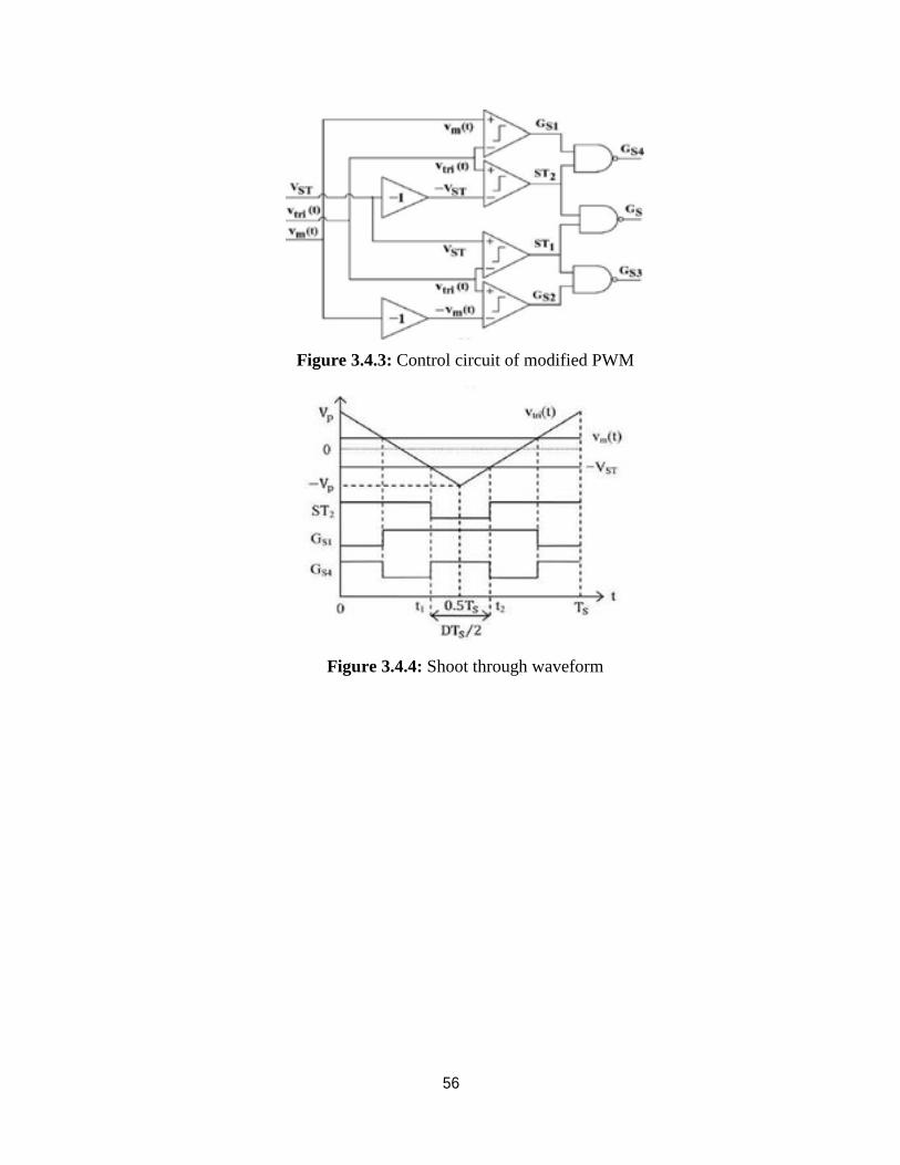
56
Figure 3.4.3: Control circuit of modified PWM
Figure 3.4.4: Shoot through waveform

57
3.5 Simulation Results
Simulation results for the two PWM techniques will be presented and comparison of switched boost
inverter and conventional Z source inverter will be investigate. Changing the value of VST will lead a
change in the duty ratio D of the shoot through mode as shown in Figure 3.6. The relationship between
VST and D is given by (3.27). The output voltage waveform vAB and the input voltage waveform Vi is
shown in Figure 3.8. There are five inters for the output voltage, three of them are zero states and two are
power states i.e. vAB = 0 and vAB = VC respectively. This occurs in one switching period and the five states
occur in one switching cycle. The duty ratio D selection is necessary to overlap of the shoot through phase
and power phase, expressions (3.28) to
(3.29) helps in resolving that. The parameters used for the simulation of the two cases of switched boost
inverter are given in Table 1.
D = 1 - 𝑉𝑆𝑇
𝑉𝑃 (3.27)
[𝐷. 𝑇𝑆 < 𝑇𝑆 −max(𝑣𝑚(𝑡).𝑇𝑆
𝑉𝑃)], D < 1 - M (3.28)
M = max [𝑣𝑚(𝑡)
𝑉𝑃 ] (3.29)
The maximum fundamental component of the output voltage expression is given by (3.30):
vAB = M [1−𝐷
1−2𝐷] vg= M.VC (3.30)
Figure 3.5.1: SBI circuit for simulation

58
Table 3.5.1: Simulation Parameters
SWITCHED BOOST INVERTER
Component Conventional PWM Modified PWM
Input Voltage Vi 64 64
Impedance inductor L 5.6mH 5.6mH
Filter inductor Lf 4.6mH 4.6mH
Impedance capacitor C 470F 470F
Impedance Capacitor Cf 10F 10F
Load resistor Ro 25ohm 25ohm
Switching frequency fo 5kHz 5kHz
D_Ref1 0.8 0.8
D_Ref2 0.4
D_VST - 0.6
D_Vm - 0.5
Simulation results for the first PWM method i.e. conventional pulse width modulation method as
discussed in the above literature is shown below:
Figure 3.5.2: SBI circuit for simulation

59
Figure 3.5.3: SBI circuit for simulation
Simulation results for the second PWM method ie modified pulse width modulation technique as
discussed in the above literature is shown below:
Figure 3.5.4: SBI circuit for simulation

60
Figure 3.5.5: SBI circuit for simulation
Simulation results for the first PWM method i.e. conventional pulse width modulation method as
discussed in the above literature is shown in Figure 3.10 and Figure 3.11. In Figure 3.11 the two reference
signals (Ref1 and Ref2) output waveforms together with the control signals of gates G1 to G4 are shown.
The carrier signal is given by vtri. Also the shoot through states ST1 and ST2 together produces the
control signal for gate Gs. Figure 3.11 shows the component voltage and current, the input and output
voltage are also shown. The capacitor voltage and switch voltage are represented by vC and Vsn, the
source voltage and the inverter bridge input which is also the output voltage of the Z source network are
given by Vi and Vdc respectively. It should be noted that LfCf filter is connected at the output and V01 is
the output voltage before the filter and V02 is the output voltage after the filter. Figure 3.12 and Figure
3.13 show the output waveforms for the second PWM method which is the modified PWM. The
parameters of the graph for the two control methods are similar the difference lies in the carrier signal
and the method for generating the various gate signals.

61
CHAPTER 4
CONCLUSION AND RECOMMENDATIONS
4.1 Conclusion
Voltage source inverters have wide areas of applications because the input is voltage source and it’s
suitable for many applications which require voltage source as the input. Variable or adjustable speed
drives and FACTS devices are some major of the major applications areas of voltage source inverters.
Although VSI can be applied to high power system, it’s most suitable in medium power applications
because they are able to generate output voltage with very high quality waveforms. The voltage source
inverter also known as voltage source converter (when used for both inversion and rectifying purposes)
has wide areas of applications but it’s fraught with many limitations such: it’s a buck or step down inverter
that’s the output voltage is always less than the input voltage unless a buck-boost converter is applied.
When used as a rectifier, it’s a boost rectifier circuit, applications of buck-boost converter in VSI topology
increases the cost of the unit, reduces the efficiency of the system and complicated control technique is
introduced, shoot through property is absent in VSI or CSI hence EMIs immunity is absent, inductor –
capacitor filter is required to reduce power systems noises. Current source inverters have some limitations
such as: the current source inverter is a boost inverter. and when applied as rectifier, it’s a buck rectifier
circuit, buck dc converters are required to reduce the cost hence, cost of system and efficiency increases
and reduces respectively, Open circuit on a load side is a big problem when preventive measures are not
taken and reverse voltage path should be provide or blocked.
The introduction of Z source or impedance networks into VSI and CSI topologies solves the problems of
buck or boost quality depending on the structure and shoot through property of ZSI provides immunity to
the effects of EMIs and boost the voltage gain proportions of ZSI based inverters. The conventional Z
source based inverter solves major drawbacks of VSI and CSI but they also introduce some limitations
such as increased cost and size hence they are not appropriate for use in low power systems when they
following factors are off great concern; cost, weight and size.
62
The switched boost inverter topology (SBI) was introduced to solve the limitations of the traditional
impedance source inverter (ZSI). Due the sheer size of capacitor required to in LC network of ZSI, the
size, weight and cost of ZSI topology is significant increased and low power systems are not appropriate
areas for usage or application. The switched boost inverter is made up two passive components; inductor
and capacitor and two passive switch components; diodes and one active switch component; IGBT. SBI
retains all the advantages of the traditional ZSI plus merits of reduced passive components in the SBI
structure.
Comparing the SBI and ZSI topologies shows that the two topologies have similar mathematical equations
except in the case of dc link voltage where the SBI’s value is lower due to this equation 1 – D. In the case
of component count, SBI topology has reduced number of passive components but an increase in the
active and passive switch components. Due to the introduction of the active switch component in the
switched boost topology, the SBI can be viewed as an active realization of the ZSI topology. The total
number of components in the two topologies are five each and but ZSI has one capacitor more than SBI
hence the structure of SBI is minimized, the weight and cost of the structure is also reduced. Detailed
explanations of components stress is done experimentally in (Ravindranath, A et al, 2013). Analysis and
PWM control of switched boost inverter. IEEE Transactions on industrial electronics, 60(12), 5593-5602,
( Mohan, N., & Undeland, T. M., 1995) where its confirmed that SBI has lower peak voltage for the dc
link hence the voltage stress on the inverter bridge components is less; the comparison was based on same
input parameters for ZSI and SBI but the modulation index in SBI is much higher than that of ZSI. Also
it’s confirmed that the switch utilization ratio for the two topologies are almost same. Both ZSI and SBI
are able to protect inverter bridge components in the advent of shoot through caused electromagnetic
noise interference or short circuit faults; this advantage is lacked in VSI and CSI topologies. However,
the SBI has some drawbacks when compared to ZSI; increased number of diodes and switches i.e. one
diode and an extra switch is introduced in the SBI topology. Switching losses will increase the SBI due
to the extra switch. More semiconductor switches means superior defense mechanism is required to
protect the switches but current in the SBI topology is consistently limited due to the inductor. The dc
link voltage (1 – D) is also less in SBI topology; to achieve same dc link voltage levels as in ZSI topology,
higher modulation index is required.
SBI topology was presented in this thesis and simulation done for two PWM control methods;
conventional and modified. Comparison of SBI and ZSI was also investigated.

63
4.2 Recommendations
Although switched Boost inverter topology offers better boosting capabilities when compared
conventional Z source inverter, the introduction of the active switch into the structure increases the cost
of and losses the inverter. In the case of losses, conduction and switching losses are present in the SBI
topology whiles only conduction losses are present conventional ZSI. The cost is increased also because
the trigger circuit which is not required in the conventional ZSI. For future work, a detailed investigation
of the two topologies ZSI and SBI should be investigated with reference to financial cost for a period of
time to determine the best topology for practical applications.

64
REFERENCES
Abu-Rub, H., Iqbal, A., Ahmed, S. M., Peng, F. Z., Li, Y., & Baoming, G. (2013). Quasi-Z-source
inverter-based photovoltaic generation system with maximum power tracking control using
ANFIS. IEEE Transactions on Sustainable Energy, 4(1), 11-20.
Abutbul, O., Gherlitz, A., Berkovich, Y., & Ioinovici, A. (2003). Step-up switching-mode converter with
high voltage gain using a switched-capacitor circuit. IEEE Transactions on Circuits and Systems
I: Fundamental Theory and Applications, 50(8), 1098-1102..
Adamowicz, M., Strzelecki, R., Peng, F. Z., Guzinski, J., & Rub, H. A. (2011, August). New type LCCT-
Z-source inverters. In Power Electronics and Applications (EPE 2011), Proceedings of the 2011-
14th European Conference on (pp. 1-10). IEEE.
Adda, R., Joshi, A., & Mishra, S. (2013, September). Pulse width modulation of three-phase switched
boost inverter. In Energy Conversion Congress and Exposition (ECCE), 2013 IEEE (pp. 769-
774). IEEE.
Ahmadzadeh, T., & Babaei, E. (2015, February). ZH buck converter: Analysis and simulation. In Power
Electronics, Drives Systems & Technologies Conference (PEDSTC), 2015 6th (pp. 436-441).
IEEE.
Ahmadzadeh, T., & Babaei, I. (2018, February). Improved quasi-Z-source based three-phase three-level
neutral point clamped inverter. In Power Electronics, Drives Systems and Technologies
Conference (PEDSTC), 2018 9th Annual (pp. 99-103). IEEE..
Ahmed, H. F., Cha, H., Kim, S. H., & Kim, H. G. (2016). Switched-coupled-inductor quasi-Z-source
inverter. IEEE Transactions on Power Electronics, 31(2), 1241-1254.
Alcazar, Y. J. A., de Souza Oliveira, D., Tofoli, F. L., & Torrico-Bascopé, R. P. (2013). DC–DC
nonisolated boost converter based on the three-state switching cell and voltage multiplier
cells. IEEE Transactions on Industrial Electronics, 60(10), 4438-4449.
Anderson, J., & Peng, F. Z. (2008, June). Four quasi-Z-source inverters. In Power Electronics Specialists
Conference, 2008. PESC 2008. IEEE (pp. 2743-2749). IEEE..
Axelrod, B., Berkovich, Y., & Ioinovici, A. (2003, May). Transformerless DC-DC converters with a very
high DC line-to-load voltage ratio. In Circuits and Systems, 2003. ISCAS'03. Proceedings of the
2003 International Symposium on (Vol. 3, pp. III-III). IEEE.
Bratcu, A. I., Munteanu, I., Bacha, S., Picault, D., & Raison, B. (2011). Cascaded dc–dc converter
photovoltaic systems: Power optimization issues. IEEE Transactions on Industrial

65
Electronics, 58(2), 403-411.
Cha, H., Li, Y., & Peng, F. Z. (2016). Practical layouts and DC-rail voltage clamping techniques of Z-
source inverters. IEEE Transactions on Power Electronics, 31(11), 7471-7479.
Chen, X., Fu, Q., & Infield, D. G. (2009, April). PV grid-connected power conditioning system with Z-
source network. In Sustainable Power Generation and Supply, 2009. SUPERGEN'09.
International Conference on (pp. 1-6). IEEE.
Chiang, G. T., & Itoh, J. I. (2013). Comparison of two overmodulation strategies in an indirect matrix
converter. IEEE Transactions on Industrial Electronics, 60(1), 43-53.
Cintron-Rivera, J. G., Li, Y., Jiang, S., & Peng, F. Z. (2011, March). Quasi-Z-source inverter with energy
storage for photovoltaic power generation systems. In Applied power electronics conference and
exposition (APEC), 2011 twenty-sixth annual IEEE (pp. 401-406). IEEE.
Do, D. T., & Nguyen, M. K. (2018). Three-Level Quasi-Switched Boost T-Type Inverter: Analysis, PWM
Control, and Verification. IEEE Transactions on Industrial Electronics, 65(10), 8320-8329.
Dong, S., Zhang, Q., & Cheng, S. (2015). Analysis of critical inductance and capacitor voltage ripple for
a bidirectional Z-source inverter. IEEE Transactions on Power Electronics, 30(7), 4009-4015.
Emadi, A. (2014). Advanced electric drive vehicles. CRC Press.
Empringham, L., Kolar, J. W., Rodriguez, J., Wheeler, P. W., & Clare, J. C. (2013). Technological issues
and industrial application of matrix converters: A review. IEEE Transactions on Industrial
Electronics, 60(10), 4260-4271.
Gajanayake, C. J., Luo, F. L., Gooi, H. B., So, P. L., & Siow, L. K. (2010). Extended-boost $ Z $-source
inverters. IEEE Transactions on Power Electronics, 25(10), 2642-2652.
Garcia-Vite, P. M., Mancilla-David, F., & Ramirez, J. M. (2013). Per-sequence vector-switching matrix
converter modules for voltage regulation. IEEE transactions on industrial electronics, 60(12),
5411-5421.
Ge, B., Peng, F. Z., Abu-Rub, H., Ferreira, F. J., & de Almeida, A. T. (2014). Novel energy stored single-
stage photovoltaic power system with constant DC-link peak voltage. IEEE Transactions on
Sustainable Energy, 5(1), 28-36.
González-Santini, N. S., Zeng, H., Yu, Y., & Peng, F. Z. (2016). Z-source resonant converter with power
factor correction for wireless power transfer applications. IEEE Transactions on Power
Electronics, 31(11), 7691-7700.
66
Gu, B., Dominic, J., Lai, J. S., Zhao, Z., & Liu, C. (2013). High boost ratio hybrid transformer DC–DC
converter for photovoltaic module applications. IEEE Transactions On Power Electronics, 28(4),
2048-2058.
Guo, F., Fu, L., Lin, C. H., Li, C., Choi, W., & Wang, J. (2013). Development of an 85-kW bidirectional
quasi-Z-source inverter with DC-link feed-forward compensation for electric vehicle
applications. IEEE Transactions on Power Electronics, 28(12), 5477-5488..
Han, S. H., Kim, H. G., Gu, B. G., Cha, H., Chun, T. W., & Nho, E. C. (2015, June). Induction motor
control system using bidirectional quasi-Z source inverter. In Power Electronics and ECCE Asia
(ICPE-ECCE Asia), 2015 9th International Conference on (pp. 588-593). IEEE.
Hu, S., Liang, Z., & He, X. (2016). Ultracapacitor-battery hybrid energy storage system based on the
asymmetric bidirectional Z-source topology for EV. IEEE Transactions on Power
Electronics, 31(11), 7489-7498.
Hu, S., Liang, Z., Fan, D., & He, X. (2016). Hybrid ultracapacitor–battery energy storage system based
on quasi-Z-source topology and enhanced frequency dividing coordinated control for EV. IEEE
Transactions on Power Electronics, 31(11), 7598-7610.
Husev, O., Roncero-Clemente, C., Romero-Cadaval, E., Vinnikov, D., & Stepenko, S. (2014). Single
phase three-level neutral-point-clamped quasi-Z-source inverter. IET Power Electronics, 8(1), 1-
10.
J. W. Kolar, T. Friedli, J. Rodriguez, P. W. Wheeler, "Review of three-phase PWM ac-ac converter
topologies", IEEE Trans. Ind. Electron., vol. 58, no. 11, pp. 4988-5006, Nov. 2011.
Jiang, S., Cao, D., & Peng, F. Z. (2011, March). High frequency transformer isolated Z-source inverters.
In Applied Power Electronics Conference and Exposition (APEC), 2011 Twenty-Sixth Annual
IEEE (pp. 442-449). IEEE.
Karaman, E., Farasat, M., & Trzynadlowski, A. M. (2014). A comparative study of series and cascaded
Z-source matrix converters. IEEE Transactions on Industrial Electronics, 61(10), 5164-5173.
Karaman, E., Farasat, M., & Trzynadlowski, A. M. (2014). A comparative study of series and cascaded
Z-source matrix converters. IEEE Transactions on Industrial Electronics, 61(10), 5164-5173.
Khosravi, F., Azli, N. A., & Kaykhosravi, A. (2014). Design of a reduced component count single-phase
to three-phase quasi-Z-source converter. IET Power Electronics, 7(3), 489-495.
Kolar, J. W., Schafmeister, F., Round, S. D., & Ertl, H. (2007). Novel three-phase AC–AC sparse matrix
converters. IEEE transactions on power electronics, 22(5), 1649-1661.

67
LaBella, T., & Lai, J. S. (2014). A hybrid resonant converter utilizing a bidirectional GaN AC switch for
high-efficiency PV applications. IEEE Transactions on Industry Applications, 50(5), 3468-3475.
Lei, Q., Cao, D., & Peng, F. Z. (2014). Novel loss and harmonic minimized vector modulation for a
current-fed quasi-Z-source inverter in HEV motor drive application. IEEE Trans. Power
Electron, 29(3), 1344-1357.
Li, D., Loh, P. C., Zhu, M., Gao, F., & Blaabjerg, F. (2013). Generalized multicell switched-inductor and
switched-capacitor Z-source inverters. IEEE Transactions on Power Electronics, 28(2), 837-848.
Li, F., Ge, B., Sun, D., Bi, D., Peng, F. Z., & Haitham, A. R. (2011, August). Quasi-Z source inverter
with battery based PV power generation system. In Electrical Machines and Systems (ICEMS),
2011 International Conference on (pp. 1-5). IEEE.
Li, W., & He, X. (2011). Review of nonisolated high-step-up DC/DC converters in photovoltaic grid-
connected applications. IEEE Transactions on Industrial Electronics, 58(4), 1239-1250.
Liang, T. J., Chen, S. M., Yang, L. S., Chen, J. F., & Ioinovici, A. (2012). Ultra-large gain step-up
switched-capacitor DC-DC converter with coupled inductor for alternative sources of
energy. IEEE Transactions on Circuits and Systems I: Regular Papers, 59(4), 864-874.
Liang, W., Liu, Y., Ge, B., Abu-Rub, H., Balog, R. S., & Xue, Y. (2018). Double-Line-Frequency Ripple
Model, Analysis, and Impedance Design for Energy-Stored Single-Phase Quasi-Z-Source
Photovoltaic System. IEEE Transactions on Industrial Electronics, 65(4), 3198-3209.
Liang, Z., Hu, S., Hu, S., Li, W., & He, X. (2015, September). Estimation and control of battery charging
current for the asymmetrical Z-source topology in the HESS application. In Energy Conversion
Congress and Exposition (ECCE), 2015 IEEE (pp. 6180-6186). IEEE.
Liu, C., & Lai, J. S. (2007). Low frequency current ripple reduction technique with active control in a
fuel cell power system with inverter load. IEEE Transactions on Power Electronics, 22(4), 1429-
1436.
Liu, X., Wang, P., Loh, P. C., & Blaabjerg, F. (2013). A three-phase dual-input matrix converter for grid
integration of two AC type energy resources. IEEE Transactions on Industrial Electronics, 60(1),
20-30.
Liu, Y., Ge, B., Abu-Rub, H., & Peng, F. Z. (2014). Phase-shifted pulse-width-amplitude modulation for
quasi-Z-source cascade multilevel inverter-based photovoltaic power system. IET Power
Electronics, 7(6), 1444-1456.
68
Liu, Y., Ge, B., Abu-Rub, H., & Sun, D. (2015). Comprehensive modeling of single-phase quasi-Z-source
photovoltaic inverter to investigate low-frequency voltage and current ripple. IEEE Transactions
on Industrial Electronics, 62(7), 4194-4202.
Loh, P. C., & Blaabjerg, F. (2013). Magnetically coupled impedance-source inverters. IEEE Transactions
on Industry Applications, 49(5), 2177-2187.
Loh, P. C., Li, D., & Blaabjerg, F. (2013). Γ-Z-source inverters. IEEE transactions on Power
Electronics, 28(11), 4880-4884..
Luo, F. L., & Ye, H. (2004). Positive output multiple-lift push-pull switched-capacitor Luo-
converters. IEEE transactions on industrial electronics, 51(3), 594-602.
Mo, W., Loh, P. C., & Blaabjerg, F. (2014). Asymmetrical $\Gamma $-Source Inverters. IEEE
Transactions on Industrial Electronics, 61(2), 637-647..
Mohan, N., & Undeland, T. M. (2007). Power electronics: converters, applications, and design. John
Wiley & Sons.
Musavi, F., Edington, M., Eberle, W., & Dunford, W. G. (2012). Evaluation and efficiency comparison
of front end AC-DC plug-in hybrid charger topologies. IEEE Transactions on Smart grid, 3(1),
413-421.
Nguyen, M. K., Duong, T. D., Lim, Y. C., & Kim, Y. G. (2018). Switched-Capacitor Quasi-Switched
Boost Inverters. IEEE Transactions on Industrial Electronics, 65(6), 5105-5113.
Nguyen, M. K., Lim, Y. C., & Cho, G. B. (2011). Switched-inductor quasi-Z-source inverter. IEEE
Transactions on Power Electronics, 26(11), 3183-3191.
Nguyen, M. K., Lim, Y. C., & Cho, G. B. (2011). Switched-inductor quasi-Z-source inverter. IEEE
Transactions on Power Electronics, 26(11), 3183-3191..
Nguyen, M. K., Lim, Y. C., & Cho, G. B. (2011). Switched-inductor quasi-Z-source inverter. IEEE
Transactions on Power Electronics, 26(11), 3183-3191.
Nguyen, M. K., Lim, Y. C., & Kim, Y. G. (2013). TZ-source inverters. IEEE Transactions on Industrial
Electronics, 60(12), 5686-5695..
Nguyen, M. K., Lim, Y. C., Choi, J. H., & Cho, G. B. (2016). Isolated High Step-Up DC-DC Converter
Based on Quasi-Switched-Boost Network. IEEE Trans. Industrial Electronics, 63(12), 7553-7562.
Nymand, M., & Andersen, M. A. (2010). High-efficiency isolated boost DC–DC converter for high-
power low-voltage fuel-cell applications. IEEE Transactions on Industrial Electronics, 57(2), 505-
514.
69
Ott, S., Roasto, I., Vinnikov, D., & Lehtla, T. (2011). Analytical and experimental investigation of neutral
point clamped quasi-impedance-source inverter.
Peng, F. Z., Shen, M., & Holland, K. (2007). Application of Z-source inverter for traction drive of fuel
cell—Battery hybrid electric vehicles. IEEE Transactions on Power Electronics, 22(3), 1054-
1061.
Peng, F. Z., Shen, M., & Qian, Z. (2005). Maximum boost control of the Z-source inverter. IEEE
Transactions on power electronics, 20(4), 833-838.
Peng, F. Z., Yuan, X., Fang, X., & Qian, Z. (2003). Z-source inverter for adjustable speed drives. IEEE
power electronics letters, 1(2), 33-35.
Pilehvar, M. S., & Mardaneh, M. (2014, February). Novel approaches for phase-shift control and
harmonics reduction in H-bridge Z-source inverter. In Power Electronics, Drive Systems and
Technologies Conference (PEDSTC), 2014 5th(pp. 445-451). IEEE.
Pires, V. F., Cordeiro, A., Foito, D., & Martins, J. F. (2016). Quasi-Z-source inverter with a T-type
converter in normal and failure mode. IEEE Transactions on Power Electronics, 31(11), 7462-
7470.
Pires, V. F., Romero-Cadaval, E., Vinnikov, D., Roasto, I., & Martins, J. F. (2014). Power converter
interfaces for electrochemical energy storage systems–A review. Energy Conversion and
Management, 86, 453-475.
Potamianos, P. G., Mitronikas, E. D., & Safacas, A. N. (2014). Open-circuit fault diagnosis for matrix
converter drives and remedial operation using carrier-based modulation methods. IEEE
Transactions on Industrial Electronics, 61(1), 531-545.
Prudente, M., Pfitscher, L. L., Emmendoerfer, G., Romaneli, E. F., & Gules, R. (2008). Voltage multiplier
cells applied to non-isolated DC–DC converters. IEEE Transactions on Power Electronics, 23(2),
871-887.
Q. Zhao and F. C. Lee, “High-efficiency, high step-up dc–dc converters,” IEEE Trans. Power Electron.,
vol. 18, no. 1, pp. 65–73, Jan. 2003.
Qian, W., Peng, F. Z., & Cha, H. (2011). Trans-Z-source inverters. IEEE transactions on power
electronics, 26(12), 3453-3463.
Rajakaruna, S., & Jayawickrama, L. (2010). Steady-state analysis and designing impedance network of
Z-source inverters. IEEE Transactions on Industrial Electronics, 57(7), 2483-2491.

70
Ravindranath, A., Mishra, S. K., & Joshi, A. (2013). Analysis and PWM control of switched boost
inverter. IEEE Transactions on industrial electronics, 60(12), 5593-5602.
Shahinpour, A., Moghani, J. S., Gharehpetian, G. B., & Abdi, B. (2014, February). High gain high-voltage
z-source converter for offshore wind energy systems. In Power Electronics, Drive Systems and
Technologies Conference (PEDSTC), 2014 5th (pp. 488-493). IEEE.
Shen, H., Zhang, B., Qiu, D., & Zhou, L. (2016). A common grounded Z-source DC–DC converter with
high voltage gain. IEEE Transactions on Industrial Electronics, 63(5), 2925-2935.
Shen, M., Wang, J., Joseph, A., Peng, F. Z., Tolbert, L. M., & Adams, D. J. (2006). Constant boost control
of the Z-source inverter to minimize current ripple and voltage stress. IEEE transactions on
industry applications, 42(3), 770-778..
Siwakoti, Y. P., Blaabjerg, F., & Loh, P. C. (2016). New magnetically coupled impedance (Z-) source
networks. IEEE Trans. Power Electron, 31(11), 7419-7435..
Song, W., Zhong, Y., Zhang, H., Sun, X., Zhang, Q., & Wang, W. (2013). A study of Z-source dual-
bridge matrix converter immune to abnormal input voltage disturbance and with high voltage
transfer ratio. IEEE Transactions on Industrial Informatics, 9(2), 828-838.
Strzelecki, R., Adamowicz, M., Strzelecka, N., & Bury, W. (2009, May). New type T-source inverter.
In Compatibility and Power Electronics, 2009. CPE'09. (pp. 191-195). IEEE.
Sun, D., Ge, B., Liang, W., Abu-Rub, H., & Peng, F. Z. (2015). An energy stored quasi-Z-source cascade
multilevel inverter-based photovoltaic power generation system. IEEE Transactions on
Industrial Electronics, 62(9), 5458-5467.
Sun, D., Ge, B., Peng, F. Z., Rub, H. A., & de Almeida, A. T. (2011, September). Power flow control for
quasi-Z source inverter with battery based PV power generation system. In Energy Conversion
Congress and Exposition (ECCE), 2011 IEEE (pp. 1051-1056). IEEE.
Tang, Y., Fu, D., Wang, T., & Xu, Z. (2015). Hybrid Switched-Inductor Converters for High Step-Up
Conversion. IEEE Trans. Industrial Electronics, 62(3), 1480-1490.
Thang, T. V., Thao, N. M., Jang, J. H., & Park, J. H. (2014). Analysis and design of grid-connected
photovoltaic systems with multiple-integrated converters and a pseudo-dc-link inverter. IEEE
Transactions on industrial electronics, 61(7), 3377-3386.
Tran, T. T., & Nguyen, M. K. (2017). Cascaded five-level quasi-switched-boost inverter for single-phase
grid-connected system. IET Power Electronics, 10(14), 1896-1903.

71
Tseng, K. C., & Huang, C. C. (2014). High step-up high-efficiency interleaved converter with voltage
multiplier module for renewable energy system. IEEE transactions on industrial electronics, 61(3),
1311-1319.
Wai, R. J., & Duan, R. Y. (2005). High step-up converter with coupled-inductor. IEEE Transactions on
Power Electronics, 20(5), 1025-1035.
Walker, G. R., & Sernia, P. C. (2004). Cascaded DC-DC converter connection of photovoltaic
modules. IEEE transactions on power electronics, 19(4), 1130-1139..
Wang, J., Wu, B., Xu, D., & Zargari, N. R. (2013). Indirect space-vector-based modulation techniques
for high-power multimodular matrix converters. IEEE Transactions on Industrial
Electronics, 60(8), 3060-3071..
Wang, J., Wu, B., Xu, D., & Zargari, N. R. (2013). Phase-shifting-transformer-fed multimodular matrix
converter operated by a new modulation strategy. IEEE Transactions on Industrial
Electronics, 60(10), 4329-4338.
Wu, G., Ruan, X., & Ye, Z. (2015). Nonisolated high step-up DC–DC converters adopting switched-
capacitor cell. IEEE Transactions on Industrial Electronics, 62(1), 383-393.
Xia, C., Zhao, J., Yan, Y., & Shi, T. (2014). A Novel Direct Torque Control of Matrix Converter-Fed
PMSM Drives Using Duty Cycle Control for Torque Ripple Reduction. IEEE Trans. Industrial
Electronics, 61(6), 2700-2713.D. Cao, S. Jiang,
X. Yu, F. Z. Peng, "Low-cost semi-Z-source inverter for single-phase photovoltaic systems", IEEE Trans.
Power Electron., vol. 26, no. 12, pp. 3514-3523, Dec. 2011.
Xu, P., Zhang, X., Zhang, C. W., Cao, R. X., & Chang, L. (2006, June). Study of Z-source inverter for
grid-connected PV systems. In Power Electronics Specialists Conference, 2006. PESC'06. 37th
IEEE (pp. 1-5). IEEE.
Xue, Y., Chang, L., Kjaer, S. B., Bordonau, J., & Shimizu, T. (2004). Topologies of single-phase inverters
for small distributed power generators: an overview. IEEE transactions on Power
Electronics, 19(5), 1305-1314.
Xue, Y., Ge, B., & Peng, F. Z. (2012, September). Reliability, efficiency, and cost comparisons of MW-
scale photovoltaic inverters. In Energy Conversion Congress and Exposition (ECCE), 2012
IEEE (pp. 1627-1634). IEEE.

72
Yi, F., & Cai, W. (2016). A quasi-Z-source integrated multiport power converter as switched reluctance
motor drives for capacitance reduction and wide-speed-range operation. IEEE Transactions on
Power Electronics, 31(11), 7661-7676.
Yilmaz, M., & Krein, P. T. (2013). Review of battery charger topologies, charging power levels, and
infrastructure for plug-in electric and hybrid vehicles. IEEE Transactions on Power
Electronics, 28(5), 2151-2169.
Zhang, J., & Ge, J. (2010, March). Analysis of Z-source DC-DC converter in discontinuous current mode.
In Power and Energy Engineering Conference (APPEEC), 2010 Asia-Pacific(pp. 1-4). IEEE.
Zhou, Y., Liu, L., & Li, H. (2013). A high-performance photovoltaic module-integrated converter (MIC)
based on cascaded quasi-Z-source inverters (qZSI) using eGaN FETs. IEEE Transactions on
Power Electronics, 28(6), 2727-2738.


![The PWM Control of the Three-phase Induction Motor · [7] R. M Tallam, R. Naik, T. A. Nondah. A carrier based PWM scheme for neutral—point voltage balancing in three-level inverters](https://static.fdocuments.us/doc/165x107/6134dd0bdfd10f4dd73c00d7/the-pwm-control-of-the-three-phase-induction-motor-7-r-m-tallam-r-naik-t.jpg)


