Analysis and Design for a High Power Density Three-Phase AC Converter ... · Analysis and Design...
178
Analysis and Design for a High Power Density Three-Phase AC Converter Using SiC Devices Rixin Lai Dissertation submitted to the faculty of the Virginia Polytechnic Institute and State University in partial fulfillment of the requirements for the degree of Doctor of Philosophy In Electrical Engineering Committee: Dr. Fred Wang (Chair) Dr. Dushan Boroyevich Dr. Rolando Burgos Dr. Yilu Liu Dr. Tao Lin December 10, 2008 Blacksburg, Virginia Keywords: high power density, SiC devices, passive component minimization, topology evaluation, high performance control development, failure mode analysis
-
Upload
truongkiet -
Category
Documents
-
view
214 -
download
1
Transcript of Analysis and Design for a High Power Density Three-Phase AC Converter ... · Analysis and Design...
Analysis and Design for a High Power Density
Three-Phase AC Converter Using SiC Devices
Rixin Lai
Dissertation submitted to the faculty of the Virginia Polytechnic Institute and State University in partial fulfillment of the
requirements for the degree of
Doctor of Philosophy In
Electrical Engineering
Committee: Dr. Fred Wang (Chair) Dr. Dushan Boroyevich
Dr. Rolando Burgos Dr. Yilu Liu Dr. Tao Lin
December 10, 2008 Blacksburg, Virginia
Keywords: high power density, SiC devices, passive component minimization, topology evaluation, high performance control development,
failure mode analysis

Analysis and Design for a High Power Density
Three-Phase AC Converter Using SiC Devices
Rixin Lai
Abstract
The development of a high-power-density three-phase ac converter has been a hot
topic in power electronics due to the increasing need in applications like electric vehicles,
aircraft and aerospace, where light weight and/or a low volume is usually a must. There
are many challenges due to the complicated relationships in a three-phase power
converter system. In addition, with the emerging SiC device technology, the operating
frequency of the converter can be potentially pushed to tens of kHz to hundreds of kHz at
high-voltages and high-power conditions. The extended frequency range brings
opportunities to further improve the power density of the converter. The technologies
based on existing devices need to be revisited.
In this dissertation, a systematic methodology to analyze and design a high-power-
density three-phase ac converter is developed. All the key factors of the converter design
are investigated with the goal of high power density. The dissertation is divided into five
sections. Firstly, the criteria for passive filter selection are derived, and the relationship
between the switching frequency and the size of the EMI filter is investigated. A
functional integration concept is proposed together with the physical design approach.
Secondly, a topology evaluation method is presented, which provides insight into the

relationships between the system constraints, operating conditions and design variables.
Four topologies are then compared with the proposed approach, culminating with a
preferred topology under the given conditions. Thirdly, a novel average model is
developed for the selected topology, and is used for devising a carrier-based control
approach with simple calculations and good regulation performance. Fourthly, the
converter failure mode operation and corresponding protection approaches are discussed
and developed. Finally, a 10 kW three-phase ac/ac converter is built with the SiC devices.
All the key concepts and ideas developed in this work are implemented in this hardware
system and then verified by the experimental results.

iv
Acknowledgements
I owe an enormous debt of gratitude to my advisor, Dr. Fred Wang, for his patience,
support, guidance and belief during my study as well as my daily life. He taught me
something beyond just techniques for solving problems and led me to a new world full of
challenges and opportunities. His profound knowledge, gentle personality and rigorous
attitude toward research will benefit my career as well as my whole personal life.
I would like to express my appreciation to my committee member, Dr. Dushan
Boroyevich, who has very creative thinking and also a sense of humor, for his instruction
and many vivid ideas. I would like to thank Dr. Rolando Burgos, who always has
infectious enthusiasm on work and daily life, for his help and time at many aspects. I
would also like to thank my other committee members Dr. Yilu Liu and Dr. Tao Lin for
always helping and encouraging me during my time as a graduate student.
I would also like to thank all my colleagues in CPES for their help, mentorship, and
friendship. I cherish the wonderful time that we worked together. Although this is not a
complete list, I must mention some of those who made valuable input to my work. They
are Dr. Shuo Wang, Dr. Ming Xu, Dr. Yunqing Pei, Dr. Wei Shen, Dr. Qian Liu, Dr.
Hongfang Wang, Honggang Sheng, Jerry Francis, Carson Baisden, Tim Thacker, Ball
Arthur, Arnedo Luis, Reusch David, Doug Sterk, Dianbo Fu, Chuanyun Wang, Jing Xu,
Michele Lim, Yan Liang, Sebastian Rosado, Yoann Maillet, Yi Sun, Jian Li, Pengju
Kong, Ruxi Wang, Dong Dong, Zheng Chen, Qian Li, Xiao Cao, Tong Liu, Daocheng
Huang, Ying Lu, Jing Xue, and so many others. In particular, I would like to thank Puqi
Ning, Di Zhang, Dong Jiang and Zhiyu Shen for their help and time on this project.

v
I would like to thank the administrative staff members, Marianne Hawthorne, Robert
Martin, Teresa Shaw, Trish Rose, Elizabeth Tranter, Linda Gallagher and Dan Huff, who
always smiled at me and helped me to get things done smoothly.
I offer my deepest gratitude to my girlfriend, Yan Jiang, my aunt, Jufen Xie, my
brother, and my mom and dad, for their love, support and confidence in me.

vi
Table of Contents
Chapter 1 Introduction..................................................................................................... 1
1.1 Background......................................................................................................... 1
1.2 State-of-the-art Research .................................................................................... 8
1.3 Research Challenges and Objectives ................................................................ 13
1.4 Dissertation Organization ................................................................................. 15
Chapter 2 Passive Filter Minimization .......................................................................... 17
2.1 Introduction on Filter Design............................................................................ 17
2.2 Passive Parameters Selection and Minimization .............................................. 20
2.2.1 Switching Frequency Selection and EMI Filter Design ........................... 20
2.2.2 Boost Inductor and DC-Link Capacitor Design........................................ 30
2.2.3 Simulation Verification............................................................................. 34
2.3 Summary ........................................................................................................... 38
Chapter 3 Topology Evaluation..................................................................................... 39
3.1 Introduction....................................................................................................... 39
3.2 Evaluation Approach ........................................................................................ 42
3.3 Topology Comparison ...................................................................................... 52
3.4 Summary ........................................................................................................... 69
Chapter 4 Modeling and Control for Non-Regenerative Three-Level Boost Rectifier. 71
4.1 Introduction....................................................................................................... 71
4.2 Average Model Derivation ............................................................................... 74
4.3 Proposed Controller .......................................................................................... 79
4.4 Simulation and Experiment Results.................................................................. 82

vii
4.5 Space Vector Analysis ...................................................................................... 89
4.6 Summary ........................................................................................................... 94
Chapter 5 Failure Mode Analysis and Protection.......................................................... 95
5.1 Introduction....................................................................................................... 95
5.2 Neutral Switch Shorted Failure of Vienna-Type Rectifier ............................... 98
5.2.1 Fault Mechanism Analysis........................................................................ 98
5.2.2 Over Voltage Protection ......................................................................... 100
5.2.3 Experimental Verification....................................................................... 110
5.3 Shoot-Through Failure and Protection............................................................ 112
5.3.1 Proposed Protection Approach ............................................................... 112
5.3.2 Gate Driver Circuit Design ..................................................................... 115
5.3.3 Experiment Results ................................................................................. 117
5.4 Summary ......................................................................................................... 119
Chapter 6 Hardware Development and Experiments .................................................. 121
6.1 System Configuration and Interface ............................................................... 121
6.2 Hardware Design and Construction ................................................................ 123
6.2.1 Digital Controller .................................................................................... 123
6.2.2 DC Bus Board ......................................................................................... 124
6.2.3 Input Filter .............................................................................................. 127
6.2.4 Phase Leg Module and Gate Drive ......................................................... 129
6.2.5 SiC JFET Characterization ..................................................................... 134
6.3 System Assembly and Test ............................................................................. 135
6.3.1 System Assembly.................................................................................... 136

viii
6.3.2 Controller Structure and Start-up Sequence ........................................... 136
6.3.3 Experimental Results .............................................................................. 138
6.4 System Efficiency ........................................................................................... 144
6.5 Weight Discussion for the Hardware System ................................................. 146
6.6 Summary ......................................................................................................... 148
Chapter 7 Conclusions and Future Work .................................................................... 150
7.1 Conclusions..................................................................................................... 150
7.2 Future Work .................................................................................................... 152
Reference ........................................................................................................................ 154

ix
Table of Figures
Figure 1-1 Power density roadmap for power electronics converters [7]........................... 2
Figure 1-2 Comparison of SiC and Si based devices [9] .................................................... 3
Figure 1-3 Switching loss comparison between Si-pin diode and SiC Schottky diode [9] 4
Figure 1-4 Shipboard motor drive [11]............................................................................... 5
Figure 1-5 Weight distribution of shipboard converter system [11]................................... 5
Figure 1-6 Approaches to achieve high power density....................................................... 6
Figure 2-1 Diagram for back-to-back VSC ...................................................................... 18
Figure 2-2 Spectrum analysis for SVM ............................................................................ 22
Figure 2-3 Spectrum analysis for DPWM ........................................................................ 23
Figure 2-4 Differential mode noise................................................................................... 25
Figure 2-5 Common mode noise....................................................................................... 25
Figure 2-6 Corner frequency vs. switching frequency...................................................... 26
Figure 2-7 Two-stage EMI filter....................................................................................... 26
Figure 2-8 DM noise spectrum around the first order switching frequency..................... 29
Figure 2-9 Required inductance for power quality standard and EMI standard............... 29
Figure 2-10 Cascaded subsystem diagram........................................................................ 32
Figure 2-11 Impedance bode plot ..................................................................................... 32
Figure 2-12 Failure mode comparison for 10uF and 100uF DC link capacitance............ 34
Figure 2-13 Circuit diagram for Vienna rectifier.............................................................. 34
Figure 2-14 Simulation results for load step change (The top traces are the capacitor
voltages, the bottom traces are the source input current.)................................................. 35

x
Figure 2-15 Steady state simulation waveforms (The top traces are the input currents, the
bottom traces are the capacitor voltages.)......................................................................... 36
Figure 2-16 Harmonic current spectrum........................................................................... 37
Figure 2-17 EMI spectrum................................................................................................ 37
Figure 3-1 Key components for an ac-ac converter.......................................................... 42
Figure 3-2 Topology evaluation procedure....................................................................... 43
Figure 3-3 Device thermal structure illustration............................................................... 46
Figure 3-4 Thermal equivalent model............................................................................... 46
Figure 3-5 CL-CL filter for CSC ...................................................................................... 49
Figure 3-6 Design variables for the EE core..................................................................... 51
Figure 3-7 Design variables for the toroid core ................................................................ 51
Figure 3-8 (a) Back-to-back VSC, (b) Non-generative three-level boost rectifier plus
voltage source inverter, (c) Back-to-back CSC and (d) 12-switch matrix converter........ 53
Figure 3-9 Simulation results for BTB-VSC: (a) ac-line currents; (b) PWM line-to-line
voltage............................................................................................................................... 54
Figure 3-10 Vector synthesis in sector I of space vector diagram.................................... 55
Figure 3-11 Pulse pattern for the top switches in the first 30° ......................................... 55
Figure 3-12 Simulation results for NTR-VSI: (a) ac-line currents; (b) PWM line-to-line
voltage............................................................................................................................... 58
Figure 3-13 Spectrum of the PWM voltage for NTR-VSI ............................................... 59
Figure 3-14 Simulation results for BTB-CSC: (a) ac-line source currents; (b) rectifier
input current ...................................................................................................................... 60
Figure 3-15 Spectrum of the PWM current for BTB-CSC............................................... 60

xi
Figure 3-16 Simulation results for 12-switch matrix converter: (a) source currents; (b)
PWM line current.............................................................................................................. 63
Figure 3-17 Spectrum of the PWM current for matrix converter ..................................... 63
Figure 3-18 Weight comparison of four topologies under consideration ......................... 65
Figure 3-19 Formulation of the converter optimization ................................................... 68
Figure 4-1 Rectifier topology............................................................................................ 74
Figure 4-2 State space average model .............................................................................. 78
Figure 4-3 Neutral point voltage control loop .................................................................. 78
Figure 4-4 Time domain waveform of d0’ (M=1, ω0=400 Hz)......................................... 79
Figure 4-5 Spectrum of d0’ (M=1, ω0=400 Hz) ................................................................ 80
Figure 4-6 Control scheme diagram ................................................................................. 80
Figure 4-7 Steady state simulation results (The top traces are the voltages across the two
dc-link capacitors respectively. The bottom two traces are the input voltage and the line
current of phase A.)........................................................................................................... 83
Figure 4-8 Simulation results of load step up transient (The top traces are the dc link
voltages. The bottom traces are the input phase currents.) ............................................... 83
Figure 4-9 Voltage unbalance behavior under pulsating ∆d0 (The top trace is the
waveform of ∆d0. The bottom traces show the dc-link voltage unbalance corresponding to
the given ∆d0. The light color line is the simulation result and the dark color line is the
calculation result from the proposed model.) ................................................................... 84
Figure 4-10 Experimental system ..................................................................................... 85

xii
Figure 4-11 Experimental waveform of the transient for operation mode transition
(Traces from top to bottom: dc-link voltages, rectifier pole to pole voltage VAB, and
input current of phase A.) ................................................................................................. 86
Figure 4-12 Steady state results with the carrier-based control scheme........................... 86
Figure 4-13 Dc-link voltage unbalance with the carrier-based control scheme ............... 87
Figure 4-14 Steady state results with the space vector based control approach ............... 87
Figure 4-15 Dc-link voltage unbalance with the space vector based control approach.... 88
Figure 4-16 Measured duty cycle components of the proposed carrier-based control
scheme (The top traces are the duty cycles for three phases. The bottom trace is the zero
sequence component.)....................................................................................................... 88
Figure 4-17 Measured duty cycle components of the space vector control scheme (The
top traces are the duty cycles for three phases. The bottom trace is the zero sequence
component.) ...................................................................................................................... 89
Figure 4-18 Space vector diagram in 60º.......................................................................... 90
Figure 5-1 Circuit diagram of the non-regenerative three-level boost rectifier................ 98
Figure 5-2 Circuit structure when Qa is shorted ............................................................... 99
Figure 5-3 Simulation results during the Qa short: the top traces are capacitor voltages,
the bottom traces are input currents .................................................................................. 99
Figure 5-4 (a) Diagram for the voltage clamping protection circuit, (b) simplified circuit
for peak voltage approximation ...................................................................................... 101
Figure 5-5 Simulation results for resistor clamping ....................................................... 102
Figure 5-6 Simulation results for varistor clamping ....................................................... 103

xiii
Figure 5-7 (a) Input current waveform in positive half cycle, (b) mode 1, (c) mode 2, and
(d) mode 3 ....................................................................................................................... 105
Figure 5-8 Impact of L and k on the peak fault current .................................................. 108
Figure 5-9 Impact of L and k on the dc-link power dissipation ...................................... 108
Figure 5-10 Circuit diagram for current breaking approach........................................... 109
Figure 5-11 Simulation results for current breaking approach ....................................... 110
Figure 5-12 Experimental waveform neutral switch shorted failure without protection 111
Figure 5-13 Experimental waveform neutral switch shorted failure with current breaking
protection approach......................................................................................................... 112
Figure 5-14 Proposed protection circuit ......................................................................... 113
Figure 5-15 Modes of operation ..................................................................................... 114
Figure 5-16 Gate driver circuit for protection................................................................. 116
Figure 5-17 Experimental setup for shoot-through protection ....................................... 117
Figure 5-18 Experimental results: Traces from top to bottom: gate to source voltage of
IGBT (Vge), drain to source voltage of MOSFET (Vds), drain current of MOSFET (Id)
and collector to emitter voltage of IGBT (Vce).............................................................. 118
Figure 6-1 Hardware system circuit diagram.................................................................. 121
Figure 6-2 Hardware system interface............................................................................ 123
Figure 6-3 Structure of the controller ............................................................................. 124
Figure 6-4 Diagram of the dc bus board ......................................................................... 125
Figure 6-5 Circuit diagram of the dc bus including protection....................................... 126
Figure 6-6 Voltage sensing circuit.................................................................................. 126
Figure 6-7 Physical structure of the dc bus board........................................................... 127

xiv
Figure 6-8 Circuit diagram of the input filter ................................................................. 128
Figure 6-9 Physical structure of the input filter .............................................................. 128
Figure 6-10 Rectifier phase leg....................................................................................... 129
Figure 6-11 Inverter phase leg ........................................................................................ 129
Figure 6-12 Gate driver circuit ....................................................................................... 130
Figure 6-13 Phase leg modules ....................................................................................... 131
Figure 6-14 Test circuit for the inverter phase leg.......................................................... 131
Figure 6-15 Waveforms of top switch turn on................................................................ 132
Figure 6-16 Waveforms of top switch turn on with additional 1.5 nF capacitor............ 133
Figure 6-17 Waveforms of top switch turn off with additional 1.5 nF capacitor ........... 133
Figure 6-18 RDS,on versus temperature ............................................................................ 134
Figure 6-19 System assembling ...................................................................................... 135
Figure 6-20 Controller structure ..................................................................................... 136
Figure 6-21 Start-up sequence ........................................................................................ 137
Figure 6-22 System start-up transient waveforms .......................................................... 138
Figure 6-23 Steady state waveforms at full power ......................................................... 139
Figure 6-24 Input current spectrum analysis .................................................................. 140
Figure 6-25 EMI measurement results............................................................................ 141
Figure 6-26 Motor test setup........................................................................................... 142
Figure 6-27 Measurement results for the rectifier .......................................................... 143
Figure 6-28 Measurement results for the inverter........................................................... 143
Figure 6-29 Weight distribution of the hardware system ............................................... 147

xv
List of Tables
Table 2-1 Double Fourier Integral Limits for SVM (Phase A) ........................................ 21
Table 2-2 Outer and Inner Double Fourier Integral Limits for DPWM (Phase A) .......... 22
Table 2-3 Harmonic Current Limits ................................................................................. 27
Table 2-4 Operation Conditions and Design Results........................................................ 35
Table 3-1 System Specifications....................................................................................... 54
Table 3-2 Design Results for BTB-VSC .......................................................................... 65
Table 3-3 Design Results for NTR-VSI............................................................................ 66
Table 3-4 Design Results for BTB-CSC........................................................................... 67
Table 3-5 Design Results for 12-Switch Matrix Converter .............................................. 67
Table 4-1 Parameters Used in Simulation ........................................................................ 82
Table 5-1 Parameters Used in Experiment ..................................................................... 111
Table 6-1 Physical Parameters for the CM Choke.......................................................... 128
Table 6-2 Switching energy under different conditions (@ 25°C)................................. 134
Table 6-3 Circuit Parameters for the experiment............................................................ 139
Table 6-4 Conditions for the Motor Test ........................................................................ 142
Table 6-5 Efficiency Measurement................................................................................. 144
Table 6-6 Loss Calculation @ Estimated Junction Temperature of 56.5C .................... 145
Table 6-7 Weight Comparison........................................................................................ 147

Chapter 1
1
Chapter 1 Introduction
This chapter starts with an introduction to the background of high-power-density
three-phase ac converters. The state-of-the-art research activities in the corresponding
area are reviewed, which helps to identify this work and its originality. The challenges
and the scope of high-density design are then presented, followed by an explanation of
the structure of the dissertation.
1.1 Background
High power density is one of the key topics for the continual development of power
electronics converters [1]. Power converters are designed not only to meet the input and
output requirements, but also to achieve a low volume or a light weight in many specific
applications. The demand for reduced converter volume is usually driven by the
requirements in information technology or hybrid vehicles due to the limited space as
well as the progress of the integrated circuit technology [2]-[4]. Additionally, a low
converter weight is particularly important for applications in aircraft and avionics, where
the weight has a dramatic impact on the cost and feasibility of the operation and
maintenance [5], [6].
There has been a large increase in the power density of the power electronics
converters over the last few decades, which covers a wide range of applications and
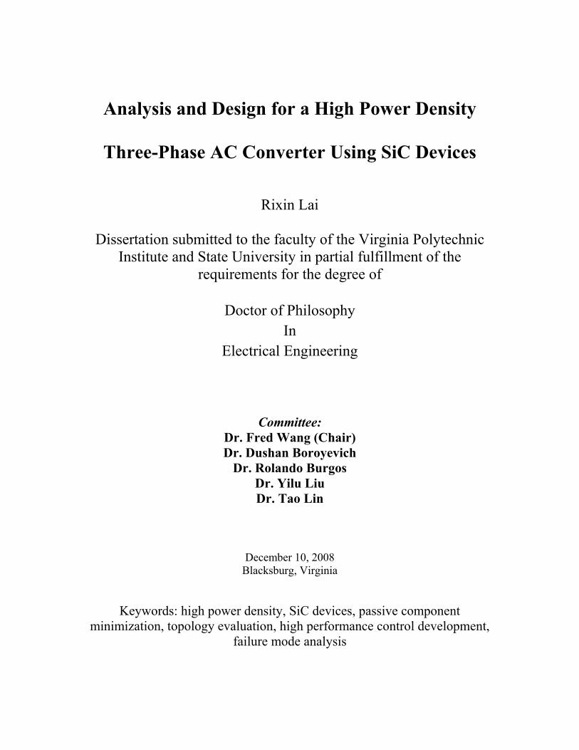
converter types. This trend is shown in Figure 1-1 [7]. The increase of power density is
mainly achieved by increasing the switching frequency, enabled by faster and lower loss
devices. In the early stages of power electronics converters, the power density was
Chapter 1
2
relatively low due to the limited speed of the available switching devices (SCR and
GTO), which usually operated at less than hundreds of Hz. Since the 1990’s, the power
density of the converter has improved greatly with the development of high-power high-
switching-frequency devices, like IGBTs and MOSFETs. Figure 1-2 indicates that further
improvement is expected in the near future with the implementation of SiC devices.
Figure 1-1 Power density roadmap for power electronics converters [7]
The SiC wide band-gap power semiconductor switches and diodes can potentially
bring significant improvement to the design of the converter system. The SiC field effect
transistor (FET) is expected to out-perform the Si IGBT and Si MOSFET in high voltage
ranges due to their low on-resistance and very fast switching characteristics [8]. Figure 1-
2 shows the static behavior of the most popular switches as well as the SiC Cascode
device [9]. For comparison, the devices are chosen with a breakdown capability of 1000
V and a 1 cm2 die size. As can be seen from Figure 1-2, the SiC switching device shows
much better performance in terms of forward voltage drop. High-voltage SiC Schottky
diodes also show very promising static and dynamic characteristics [10]. Figure 1-3

Chapter 1
3
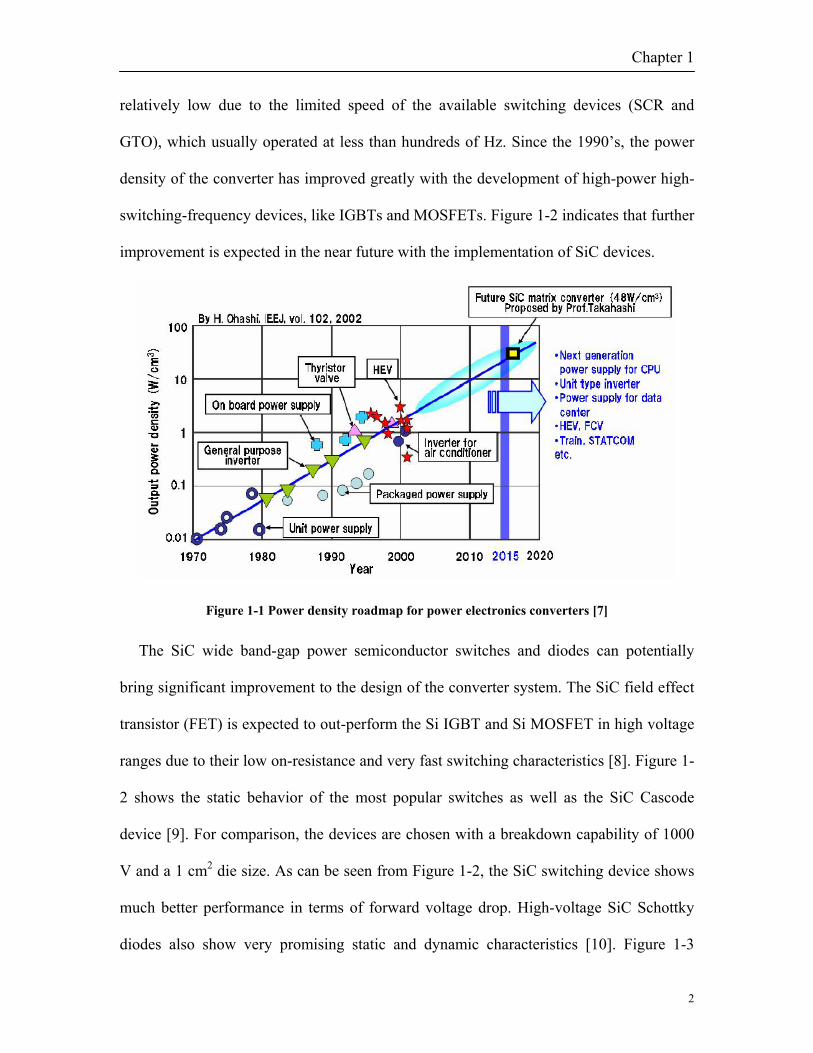
shows the switching loss of a SiC Schottky diode compared to a Si pin diode [9]. In
addition to the electrical characteristics, these devices have a higher maximum operation
junction temperature, which can potentially lead to reduced cooling effort. The features
of the SiC devices provide the possibility of a high switching frequency with low loss,
and therefore the flexibility to further improve the converter system design over a very
wide frequency range. Technology evaluation and converter design approaches based on
existing devices and materials should be revisited and modified in order to fully utilize
the SiC devices and further improve the power density. For this reason, SiC devices are
selected in this work while studying the high-density power converters.
Figure 1-2 Comparison of SiC and Si based devices [9]
Chapter 1
4
Figure 1-3 Switching loss comparison between Si-pin diode and SiC Schottky diode [9]
A power electronics converter usually consists of the following elements [1]:
• Passive filter components (input/output filter, dc-link filter)
• Cooling system
• Power semiconductors
• Control circuit and auxiliaries
• Interconnection and housing
The size and weight distribution of these elements is highly dependent on the
converter structure and the system requirements. There are thousands types of topologies
which vary with the application. Different types of topologies may require various
approaches for high-density analysis and design. This work focuses on three-phase ac
converters, since they are currently widely used in the electric transportation system

Chapter 1
5
(electric vehicle/ship/aircraft) to drive variable speed motors, where high-power-density
is usually necessary [2], [6], [11].
Figure 1-4 Shipboard motor drive [11]
Figure 1-5 Weight distribution of shipboard converter system [11]
Figure 1-4 shows the diagram for a shipboard motor drive as an example of a three-
phase ac converter [11]. The size and weight of the converter are heavily influenced by
the interface requirements that are imposed on the system. Those interface requirements
[1]

Chapter 1
6
include not only electric compatibility, such as power quality standard and EMI standards,
but also mechanical concerns, such as shock and vibration. Reference [11] carries out
example designs for two different standards, and the components weights of the whole
system are shown in Figure 1-5 [11], indicating that for both passive filter designs, the
cooling system and the housing are the key contributors to the weight. The housing
usually is related to the system profile. Its size and weight will be reduced if the overall
size is reduced. Therefore this work did not put special effort on reducing the size and
weight of the housing.
Reduce Passives
• High switching frequency• Circuit & filter topology• Components & materials• Integration
• Topology for reduced noises, losses, filter needs• SiC devices for low loss, high frequency, & high temperature• Passive materials & components • Design limit and optimization
High-density ConverterHigh-density Converter
Reduce Heatsink
• Low loss• High junction temperature• Cooling technology
Figure 1-6 Approaches to achieve high power density
There are two ways to reduce the size of the converter by changing the electrical
components. One is to reduce the passive filter; the other is to reduce the heatsink, as
shown in Figure 1-6. In order to achieve the first objective, several approaches may be
appropriate: raise the switching frequency, improve the circuit and filter topology, use
new components and materials, and use advanced integration technology. Using a higher

Chapter 1
7
switching frequency is a common practice for reducing the passive components. As
mentioned above, the feasible switching frequency range has been greatly extended by
the advanced SiC device technology, which will lead to new opportunities for higher-
density design. Different circuit topologies will have different noise levels, loss
performance, and energy storage requirements; therefore their choice will significantly
impact the size of the passive components and the heatsink. Components and materials
selection as well as the integration approach are clearly important aspects to reducing the
component size. For the heatsink reduction, the effort is on reducing the loss and
increasing the device operating junction temperature while searching for better cooling
technologies.
Although the approaches discussed above seem to be common methods in the
development of high-power-density power electronics converters, the relationship
between the overall system performance and the variables is far from well-understood by
average practitioners, especially in the extended frequency range offered by SiC devices.
In addition, implementation of SiC devices in high-power three-phase converters remains
a challenge due to lack of experience and the normally-on characteristics of the JFET
structure. Therefore there is a clear need for a systematic analysis and design approach
for high-power-density converters using SiC devices, as well as hardware implementation
and verification. The literature review in the next section shows the state-of-the-art status
of the research related to the high-power-density three-phase ac converter design and
hardware development using SiC devices, which helps to define the challenges and
research topics of this work.

Chapter 1
8
1.2 State-of-the-art Research
The analysis and design for high-density power electronics converters require a wide
area in research focus from the classical electrical aspects of topologies, passive filter
design, modulation, and control; to other aspects such as the power semiconductors,
cooling techniques, magnetic and dielectric materials, interconnection, and packaging
approaches. In this work we focus on the research in the classical electrical aspects.
From the system approach standpoint, J. W. Kolar [1] indentified and quantified the
technological barriers for high-power-density converters by investigating the volume of
the cooling system and the main passive components as functions of the switching
frequency. Analysis is carried out for 5 kW rated power while using high-performance air
cooling and advanced power semiconductors. The results indicate a volume density limit
of 45 kW/dm3 for a three-phase PWM rectifier with the present technology. This paper
provided a full vision for the design of high-density power converters in a general sense,
but the key correlations between the system requirements and the system parameters are
not clearly analyzed and reported. Y. Hayashi [7] [12] proposed a high-density power
converter design platform. A power converter is classified by four factors: the power
device, the converter circuit, including stray parameters, the passive filter, and control.
The relationships among the factors are quantified and stored in the design database, but
only the power loss estimation of the converter system was reported in this paper.
The practical approach to achieving high-density design is to investigate the key
factors one by one and try to obtain minimum weight design for each of them. Obviously
topology is one of the key factors, since it has a dramatic impact on the filter size and loss
performance. There has been some previous work on evaluating ac converter topologies

Chapter 1
9
[13]-[16]. Reference [13] compares three ac-dc converter topologies in terms of volume
and weight for application in future more-electric aircraft. The loss and the input
inductance with the corresponding current’s harmonic performance are analyzed.
Reference [14] investigated three-phase converter topologies for integrated motor drives
by discussing the hardware requirements and comparing their performance. The
evaluation effort focused on the size of the input inductance and the efficiency of the
system. Reference [15] calculated and compared the efficiency and loss distribution of
the voltage source and current source drive systems. The impact of the switching pattern
is considered, and during the comparison the optimized modulation approach is
implemented for the current-source converters. Reference [16] evaluates three-level
topologies as a replacement for two-level topologies. The input harmonic filter size and
the semiconductor loss are carefully studied. The cost and the life time are also estimated
in this paper.
In summary, the previous work discussed above focuses on specific aspects of the
converter design. The EMI filter, which is one of the main size contributors for active
front end rectifier, is usually ignored in the evaluation. Moreover, the previous work
concentrated on the evaluation and comparison of some given topologies instead of
providing a systematic analysis and selection tool. In-depth understanding of the
correlations between system variables and power density is still desired.
Another key aspect for the high-power-density converter is the passive filter
component. In terms of function, the passive filter component includes the input
harmonic filter, EMI filter, dc-link filter and output filter. The values of the passive
components are related to performance requirements, such as EMI and power quality

Chapter 1
10
standards, as well as to the switching frequency and control strategy. Habetler et al. [17]
concluded that the voltage source configuration provides the lowest passive component
size, and they also studied the effect of the modulation scheme. References [18] and [19]
designed the boost inductor based on THD and the switching ripple requirement.
Reference [20] proposed a step-by-step design procedure for the LCL filter to limit the
switching frequency ripple injection in the range of 2-150 kHz. The boost inductor and
the high-frequency stage are designed separately. For the EMI filter, reference [21]
provided guidelines for the design of a multistage structure. This study points out that the
capacitors and inductors have to be chosen with equal values in order to obtain maximum
attenuation with minimum overall capacitance and inductance. Reference [22] designed a
differential-mode input filter based on a harmonic analysis of the rectifier input current
and a mathematical model of the measurement procedure, including a line impedance
stabilization network (LISN) and the test receiver. However [21] and [22] did not
investigate the relationship between the switching frequency and the required filter size.
P. M. Barbosa [23] studied the DM filter design for a three-phase boost rectifier. The
impact of the switching frequency on the EMI filter parameters was studied based on
circuit simulation. However, the boost inductor was not considered to be part of the EMI
filter in the design stage; therefore overall minimization may not be achieved. For the dc-
link filter selection, reference [24] derived the minimum capacitance as defined in terms
of power balance. The energy variations for the input rectifier and the motor load over
one switching cycle were carefully studied. Reference [19] developed the criteria for dc-
link capacitor selection based on the zeros and poles characteristics of the system.
References [19] and [24] are highly dependent on the load condition as well as the

Chapter 1
11
control approach, and complicated calculations are required. It is difficult to directly
expand these approaches to general cases. For the passive filter, it can be concluded that
the relationship between the switching frequency and the passive parameters, especially
for the EMI filter, were not well-studied in the aforementioned work. For the input filter,
the low-frequency stage and the high-frequency stage are always designed separately,
which may lead to oversized selections.
In addition to electrical analysis and design, hardware implementation using SiC
devices is also a challenge, due to the normally-on characteristics as well as the special
gate driver requirement of JFETs, the fast switching speed, and lack of application
experience. There have been increasing research efforts for SiC device hardware
development in recent years [25] – [36]. Some of these efforts are focused on dc/dc
applications [25] – [28], where the converter topologies are relatively simple and less
fault possibility is expected. References [29] and [30] presented a 2 kW three-phase buck
rectifier with a 150 kHz switching frequency. The current source topology takes the
advantage of the normally-on characteristics. In 2003, reference [31] claimed to have
designed the first three-phase inverter using only SiC JFETs. The inverter was tested up
to 5700 W/540 Vdc with 4 kHz switching frequency. However the switching speed was
limited to 1 kV/μs with a rather large gate resistance. Also in 2003, reference [32]
presented a SiC voltage source inverter module, which was tested at 6500 W/250 Vdc
with 4 kHz. Arkansas Power Electronics International, Inc. [33] – [35] fabricated a 4 kW
high-temperature inverter module with SiC JFETs, which was tested at about 250 °C with
20 kHz switching frequency. Reference [36] presented a 100 kHz, 1.5 kW SiC sparse
matrix converter. However SiC cascode devices are utilized instead of SiC JFETs. The Si

Chapter 1
12
MOSFET in the cascade structure provides normally-off characteristics and allowed the
use of a conventional high-speed gate driver, but the Si MOSFET also limits the
maximum case temperature. Based on the reviews on the previous work for hardware
implementation, we can conclude that for the three-phase voltage source inverters using
SiC JFETs, only limited power and switching frequencies have been verified by
hardware. There is yet to be verification of a three-phase voltage source inverter using
SiC JFETs in an ac-ac converter system.
In summary, in terms of electrical design, there has been some research on various
aspects for high-power-density converter design, but an in-depth systematic
understanding and design tool are still desired. In addition, as the SiC devices advance,
the converters operate at higher frequencies and/or have higher power ratings. The
corresponding analysis and design have to cater to this need. For the hardware
implementation in three-phase converters, the performance of SiC devices was verified
with limited operating conditions. Higher power and/or higher switching frequency
operation in a full ac/ac system needs to be explored.
We need to emphasize that control design and implementation are also key issues for
high-density converters, since the higher switching frequency and smaller passive
components will lead to increasing requirements for calculation speed and control
performance. Since this depends on the topology, it will be included in the later chapters
of this work.

Chapter 1
13
1.3 Research Challenges and Objectives
According to our survey, the state-of-the-art research has investigated various aspects
of high-density design for three-phase ac converters. However the system-level
understanding and design approach, especially for the extended operation frequency
range offered by the SiC devices, is not established. The hardware verification for SiC
devices implemented in a full ac/ac system is still desired for higher switching
frequencies and/or higher-power operating conditions. Many challenges still exist due to
the complicated correlations in the three-phase power converter system and also the new
characteristics of the SiC devices.
When developing a new converter for high-density applications, the design must take
into account all aspects contributing to the converter size and weight, which requires
investigation into the correlation between all major design parameters. There is thus a
clear need for a systematic analysis considering the strong interdependence of all design
variables and constraints. For example, increasing the switching frequency generally
helps to reduce the passive size, but it also increases the converter switching loss and
therefore heat sink size. As is shown later in the work, even the relationship between the
filter size and switching frequency is not monotonous, due to changing spectrum
characteristics and the attenuation requirements of harmonic and EMI standards.
Topology is obviously another important aspect for the system design. It impacts the loss,
passive filter selection and the control requirement. Determining how to make a fair
comparison among different topologies under given conditions is still an issue. The
controller is normally not a concern in terms of power density. However, for high-
switching-frequency and high-control-bandwidth designs, the controller calculation time

Chapter 1
14
and the regulation performance may become a constraint on the system. Therefore a high-
performance control approach is desired to guarantee the design feasibility. Failure mode
analysis and the corresponding protection are also significant, especially for applications
in the aircraft and aerospace industry, where high reliability is essential [37]. The
protection circuit will impact the converter size, and its requirements vary for different
topologies, devices and passive parameters. It should be also taken into consideration
during the design stage. For the voltage source converter built with SiC JFETs, a shoot-
through failure could be a big concern for the hardware implementation due to the
normally-on characteristics of the devices.
Corresponding to the challenges discussed above, the objective of this work is to
develop a systematic methodology for the analysis and design of a three-phase high-
power-density converter using SiC devices, and to verify the developed concepts with
hardware. The dissertation accomplishes five tasks:
(1) Develops system-level criteria for minimum passive component design and selection
considering all the key correlations, and investigates the optimal physical design for
integration function.
(2) Provides a systematic tool for topology evaluation, based on which different
topologies can be fairly compared under the given conditions and constraints.
(3) Develops a mathematical model as well as a high-performance control scheme with
low calculation effort and good regulation for the selected topology.
(4) Analyzes the failure mode of the system and develops corresponding protection
approaches.

Chapter 1
15
(5) Builds a 10 kW three-phase ac/ac system using SiC devices. All the ideas and
concepts developed in this work are included and tested.
These five items form the main content of this work. A review of the relevant
literature is included within the introductory sections of each chapter.
1.4 Dissertation Organization
The dissertation presents a systematic methodology for analyzing and designing a
high-power-density three-phase ac converter. The chapters are organized as follows.
Chapter 2 starts with the standard requirements on the source side. A double Fourier
analysis is carried out to achieve the voltage noise spectrum, based on which the required
EMI filter corner frequency can be obtained. The relationship between the switching
frequency and the filter size is carefully studied. The criteria for other filter passives are
developed with the system operation requirements. A filter integration concept is
included in this chapter, as well as the physical design approach.
Chapter 3 presents a systematic methodology for the topology evaluation of three-
phase ac converters. All the design constraints, conditions and variables of the converter
system are clearly defined, and the correlations between the key factors are carefully
investigated. Based on the proposed approach, four popular topologies are evaluated and
compared with weight metrics under given conditions.
Chapter 4 develops a novel wide-frequency-range average model for the Vienna-type
rectifier, which is chosen based on the topology comparison results in Chapter 3. An
optimal zero-sequence injection is proposed for dc-link voltage balance. Using the
proposed model, a carrier-based control approach is presented for the Vienna-type

Chapter 1
16
rectifier, and a space vector representation is utilized to analyze the feasible operation
region of this control approach.
Chapter 5 analyzes a specific over-voltage failure mode that is related to the Vienna-
type rectifier topology. Two protection approaches corresponding to this failure mode are
discussed, and the impact of the input inductance is investigated. Then a novel protection
circuit for shoot-through failure is proposed and analyzed, which is also implemented
into the converter built with SiC JFETs.
Chapter 6 presents the hardware design and development of a 10 kW three-phase ac/ac
SiC converter that implements all the concepts developed in this work. The system
structure, component selection, control interface, signal sensing, circuit protection and
gate driver design are described in detail. The experimental results are presented and
analyzed.
Finally Chapter 7 summaries the entire dissertation and discusses some ideas for
future work.

Chapter 2
17
Chapter 2 Passive Filter Minimization
This chapter develops design approach for finding the lower bound of the passive
components for three-phase ac converter. Since the passive filter design highly relates to
the topology, the two-level voltage source converter is considered as an example in this
chapter. And the methodology can be extended to other three-phase ac converters. The
impact of the switching frequency on the input filter is carefully studied in this chapter
and some favored operating points are found. The rules for ac line inductance and dc-link
capacitors are also derived from the consideration of ripple and system stability. The
design approach is verified by simulation.
2.1 Introduction on Filter Design
The passive components are essential components in the converter system. They are
used to maintain the dc link voltage, attenuate the input current noise and suppress the
output surge voltage caused by the feeding cable. For the converter system with diode
bridge front end rectifier, the filter components are usually very bulky and heavy due to
its low frequency harmonics. For the converter topologies with active front end, the
interaction between the grid and the converter system can be improved and the size of the
harmonic filters can be highly reduced. But the front end system may also raise the issues
of electromagnetic interference (EMI), which requires additional filtering [38]. At some
occasions the EMI filter is also a key contributor to the size of the converter system [11].
Therefore it is still desirable to minimize the passive components value and size even in
the topologies with active front end.

Chapter 2
18
InputFilter
AC
AC
AC
A
B
C
Front EndConverter Inverter
DCLink
MOutputFilter
Figure 2-1 Diagram for back-to-back VSC
Section 2.2 mainly focuses on the parameters selection for a back-to-back voltage
source converter (VSC) with a three-phase motor load, since it is one of the most
important cases in the electric industry. Figure 2-1 shows the general configuration of an
AC active VSC with required filter with a motor load. The passive components include
DC link capacitor, AC input inductor, and the input EMI filter. In some cases the output
filter is also required according to the concerns of over voltage and over current
suppression [39] [40]. The output filter design relates to the cable length and the motor
insulation, which is not in the scope of this work.
The values of the passive components under consideration are related to the
performance requirements, as well as to the switching frequency and control strategy.
There have been some previous studies on the passive design for the rectifier and inverter
system. Habetler et al. [17] concluded that the voltage source configuration provides the
lowest passive components size, and the effect of the modulation scheme was also
studied. Ref [18] [19] designed the boost inductor based on THD and switching ripple
requirement. Ref [20] developed the criteria for LCL filter by designing the boost
inductor and the high frequency stage. Ref. [24] [41] investigated the dc link minimum
capacitance from the power balance point of view, and [19] sized the capacitors based on
the zeros and poles characteristics of the system. These studies were all based on the

Chapter 2
19
normal operation mode with specific control techniques. In addition, the EMI filter,
which can be a dominant part of the size and cost in the active front end, was not
discussed in the previous work.
Generally speaking, higher switching frequency leads to smaller passives. But that is
not necessarily true for EMI filter due to the noise spectrum. In section 2.2, the proposed
procedure for passive minimization starts with selection of modulation scheme and
switching frequencies based on EMI filter considerations. This is especially important for
high-switching frequency (>tens of kHz) converters based on advanced Si or SiC devices.
The impact of the switching frequency on the input filter is carefully studied, culminating
with some favored operating points from the EMI standpoint.
Under a given switching frequency the minimum AC line inductance and DC link
capacitance are then selected considering control, stability, power quality and dynamic
performance requirements. The impact of the DC link ripple current and the failure mode
performance on the parameter values are also investigated. In the end of this section, an
integration design concept for the input filter is presented. It indicates that the boost
inductor and the DM inductance of the EMI filter can be design as one entity for high
switching frequency applications, while in the previous works the EMI filter is normally
designed after the boost inductor is selected. In the end of this chapter, a Saber circuit
model is built and the simulation results verify the design concepts.
The discussions below use back-to-back two-level VSC as example. The approaches
can be extended to other three-phase topologies.

Chapter 2
20
2.2 Passive Parameters Selection and Minimization
2.2.1 Switching Frequency Selection and EMI Filter Design
It is well know that switching frequency has a great impact on the EMI performance of
the system. But the relationship was not well studied so far. Usually, the conducted EMI
standard starts from the frequency of 150 kHz. If the switching frequency is lower than
150 kHz the high order harmonics of the switching frequency are required to be damped
while the first order harmonic should be considered when the switching frequency is
higher than 150 kHz. Therefore the relationship between the switching frequency and the
EMI performance could be non-monotonous. In order to investigate the impact of the
switching frequency on the required attenuation, which corresponds to the filter size, a
two-level VSC as well as a commercial EMI standard for aircraft are implemented as an
example in this section.
Since the phase-leg pulsating voltage is the source for the input current ripple and EMI
noise, its spectrum is an important part for the analytical filter design. Double Fourier
integral transform is applied to determine the harmonic spectrum of the phase-leg voltage.
The harmonic components are given in complex form [42].
∫ ∫ +=f
r
f
r
s
y
y
x
xs
tntmjdcmn tdtdeVC )()(
21
0)(
20 ωω
πωω (2-1)
where Vdc is the voltage across the dc link, ωs is the switching frequency, ω0 is the
fundamental frequency. The outer integral limit yf and yr, the inner integral limit xf and
xr are determined by the modulation scheme.

Chapter 2
21
Two kinds of space vector modulation schemes are discussed in this section: center-
aligned continuous modulation (SVM) and center-aligned discontinuous modulation
(DPWM). The modulation index is defined by
dc
ph
VV
M2
= (2-2)
where phV is the amplitude of the phase voltage. Table 2-1 [42] and table 2-2 show the
outer and inner double Fourier integral limits for SVM and DPWM respectively.
Table 2-1 Double Fourier Integral Limits for SVM (Phase A)
ry fy rx (rising edge) fx (falling edge)
0 3π
)]6
cos(231[
2ππ
−+− yM )]6
cos(231[
2ππ
−+ yM
3π
π32
]cos231[
2yM+−
π ]cos
231[
2yM+
π
π32
π )]6
cos(231[
2ππ
++− yM )]6
cos(231[
2ππ
++ yM
3π
− 0 )]6
cos(231[
2ππ
++− yM )]6
cos(231[
2ππ
++ yM
π32
− 3π
− ]cos231[
2yM+−
π ]cos
231[
2yM+
π
π− π32
− )]6
cos(231[
2ππ
−+− yM )]6
cos(231[
2ππ
−+ yM

Chapter 2
22
Table 2-2 Outer and Inner Double Fourier Integral Limits for DPWM (Phase A)
ry fy rx (rising edge) fx (falling edge)
6π
− 6π
π− π
6π
π21
)6
cos(23 ππ −− yM )
6cos(
23 ππ −yM
π21
π65
))6
cos(231( ππ ++− yM ))
6cos(
231( ππ ++ yM
π65
π67
0 0
π67
π23
))6
cos(231( ππ −+− yM ))
6cos(
231( ππ −+ yM
π23
π6
11 )
6cos(
23 ππ +− yM )
6cos(
23 ππ +yM
0 0.5 1 1.5 2
x 105
0
50
100
150
200
250
300
350spectrum of the phase leg PWM voltage for SVM
frequency (Hz)
ampl
itude
of h
arm
onic
s (V
)
Figure 2-2 Spectrum analysis for SVM

Chapter 2
23
0 0.5 1 1.5 2
x 105
0
50
100
150
200
250
300
350spectrum of the phase leg PWM voltage for DPWM
frequency (Hz)
ampl
itude
of h
arm
onic
s (V
)
Figure 2-3 Spectrum analysis for DPWM
Assuming ideal switching behaviors, we can obtain the noise voltage spectrum for a
given modulation scheme based on the data of the two tables. Figure 2-2 and Figure 2-3
show the noise spectrum results for a sample three-phase boost rectifier running at 650V
DC link voltage and 40 kHz switching frequency with space vector modulation scheme
(SVM) and 60° discontinuous pulse width modulation scheme (DPWM) respectively [42].
As we can see, the amplitudes of the first switching harmonic and its adjacent side band
for DPWM are higher than those of SVM. But the amplitudes of the high order
harmonics for DPWM decrease more quickly than SVM. It indicates that DPWM will
cause higher switching current ripple. From the EMI point of view, if the switching
frequency is lower than 150 kHz, which is the starting point for radio frequency
conducted emission requirement, DPWM will lead to lower EMI noise level as it has
lower high order harmonic component. In the applications with SiC devices, the
switching frequency of tens of kilo Hertz can be achieved. The low-frequency harmonics
caused by switching is not a concern, so DPWM is favored as it has better EMI noise

Chapter 2
24
performance and lower semiconductor loss compared to SVM. All the following analysis
in this work is based on DPWM.
With the phase-leg voltage spectrum differential mode (DM) and common mode (CM)
noise can be extracted as
3cba
CMVVVV ++
= (2-3)
CMcbaDM VVV −= ),,( (2-4)
where V(a,b,c) is the phase-leg voltage spectrum, VCM and VDM are the CM and DM noise
respectively.
Figure 2-4 and Figure 2-5 show the DM and CM noise spectrum. Figure 2-6 shows the
relationship obtained between the required filter corner frequency [43] (a two-stage filter
with 80 dB attenuation is assumed, as shown in Figure 2-7) and the switching frequency
based on the DO-160E standard [44], which defines the maximum power line noise
current as 53 dBµA at 150 kHz. For simplicity, the terminal impedance of the LISN is
assumed to be 50 Ω in this analysis. A higher filter corner frequency is desirable since it
indicates a smaller filter. The non-monotonous relationship in Figure 2-6 indicates that
higher switching frequencies do not necessarily lead to higher filter corner frequencies,
unless the switching frequencies are beyond 300−500 kHz. Clearly, there are some
preferred switching frequencies, from the standpoint of input EMI filters, as can be seen
in Figure 2-6: below 40 kHz, 70 kHz, 140 kHz, or above 300-500 kHz.

Chapter 2
25
104
105
106
0
5
10
15
20
25
30
35
40
45
50DM noise of the phase leg
Frequency (Hz)
dB A
bove
1 V
olt
Figure 2-4 Differential mode noise
104 105 1060
5
10
15
20
25
30
35
40
45
50CM noise of the phase leg
Frequency
dB A
bove
1 V
olt
Figure 2-5 Common mode noise
Similar relationships can be established for other voltage levels, other topologies, or
different filter structures. In final switching frequency determination, the impacts on the
boost inductor and the loss should be also included. The result will vary with the given
specs, and will also depend on which factor plays the dominant role. As can be seen in

Chapter 2
26
the later sections, the impact of EMI filter is dominant compared to the harmonics filter
under the conditions studied in this dissertation.
Figure 2-6 Corner frequency vs. switching frequency
Figure 2-7 Two-stage EMI filter
Figure 2-6 indicates that if the switching frequency is lower than 40 kHz, the EMI
filter size will decrease while the switching frequency decreases. But at the same time the
required boost inductance will increase due to the higher switching current ripple. In
0 50 100 150 200 250 300 350 400 450 50010
15
20
25
30
35
40
Switching frequency (kHz)
Filte
r cor
ner f
requ
ency
(kH
z)
Two-stage fitler corner frequency versus switching frequency
DM filterCM filter

Chapter 2
27
addition, the power quality standard defines the harmonic current requirement which is
usually specified in the range up to 40 times of the fundamental frequency.
Table 2-3 Harmonic Current Limits
For example, Table 2-3 shows the current harmonic limits for the aircraft [44], where
I1 is the amplitude of the fundamental component. Given the 400-800 Hz fundamental
frequency range, the limit is defined up to 32 kHz. If the switching frequency locates in
this region the switching ripple current also needs to meet the power quality standard,
which brings additional requirement for the filter design. Assuming the same filter
structure, Cx1 will not have much impact on the harmonic performance since the source
impedance is usually much lower compared to the capacitor in this frequency range.
Therefore the input filter is simplified to a LCL structure for the low frequency current
harmonics. The relationship between the harmonic amplitude and the filter parameters is

Chapter 2
28
given by (2-5), where Ik and uk is the amplitude of the kth current and voltage harmonic
respectively.
LCL
uI h
h 22 ωω −⋅= (2-5)
uk can be achieved by the spectrum analysis. In this case, the DM noise spectrums
around the first order switching frequency are dominant. Figure 2-8 shows the DM noise
of the first order switching frequency for the case of 30 kHz with 800 Hz fundamental
frequency. As can be seen, the second order side band is much higher than the other side
band harmonics and therefore it will determine the filter size. On the other hand, as far as
the switching frequency is much higher than the fundamental frequency, the amplitude of
the spectrum will not change with the frequency. We can use the same amplitude value
for uk when doing the calculation for different operation point. Then with (2-5) we can
obtain the required inductance for a given harmonic limit. Figure 2-9 shows the required
inductance versus switching frequency while assuming the capacitance to be 1 μF. For
comparison the inductance to meet EMI requirement is also shown in the same figure. As
can be seen, the required inductance increases dramatically once the switching frequency
enters the range defined by the power quality standard. Although the lower switching
frequency can improve the efficiency and reduce the heatsink, the total system size may
still increases due to the tremendous increase of the inductors.
Therefore the low switching frequency boundary is selected to be 40 kHz to avoid
relatively low-order harmonics, given the 400-800 Hz fundamental frequency range. For
a different design spec, a lower or higher switching frequency range may be selected.

Chapter 2
29
2 2.2 2.4 2.6 2.8 3 3.2 3.4 3.6 3.8 4
x 104
0
20
40
60
80
100
120
Frequency (Hz)
Noi
se V
olta
ge (V
)
Figure 2-8 DM noise spectrum around the first order switching frequency
20 22 24 26 28 30 32 34 36 38 400
200
400
600
800
1000
1200
Switching Frequency (kHz)
Indu
ctan
ce (u
H)
Inductance required by PQInductance required by EMI
Figure 2-9 Required inductance for power quality standard and EMI standard

Chapter 2
30
2.2.2 Boost Inductor and DC-Link Capacitor Design
A. Boost Inductance
When determining the boost inductance, considerations are needed for AC current
harmonics, maximum ripple and inrush current. THD can be obtained with the spectrum
analysis results under a given switching frequency. It is given by
1
2)(
IL
u
THD i
i∑=
ω (2-6)
where ui is the amplitude of the harmonic voltage with order i, ωi is the harmonic
frequency, L is the harmonic inductor and I1 is the fundamental current.
Another consideration for the boost inductance design is the instantaneous switching
ripple. It should be suppressed into a reasonable level to guarantee the control feasibility
and the proper operation of the switching device [45]. The current ripple will vary as the
mains input voltage varies over a fundamental cycle. Here we only discuss the point
when the fundamental phase current reaches the peak value as it is important for the
inductor physical design. The peak current can be approximated by:
LVTMii asmpeak /)431(
21
−+= (2-7)
where M is the modulation index, im is the amplitude of the fundamental phase current, Ts
is the switching cycle and Va is the voltage of phase A at that instant. Considering the
worse case, the possible minimum modulation index and maximum peak phase voltage
should be utilized in (2-6).
During the inrush period, the rectifier works like a diode bridge, the peak current
should be constrained due to the limit of the semiconductor device. The relationship
between the peak inrush current ipeak and the passive parameters is given by

Chapter 2
31
222
43)(
21
minitialLinepeak LIVVCLi +−= (2-8)
where Vline is the line-to-line voltage, Vinitial is the initial voltage of the DC link cap when
the inrush occurs, and Im is the amplitude of the line current. With (2-6), (2-7) and (2-8),
we can determine the minimum line inductance for the given current requirement.
Actually the boost inductor can also be a part of the EMI filter. So the total input
inductance should be the larger one between the two values designed for the EMI filter
and the line inductor respectively. Therefore the input filter can be designed as one entity
to achieve both harmonic filtering and EMI suppression. For high switching frequency
cases, the required harmonic attenuation is small. There is an opportunity to use only
EMI filter as the whole input filter since the leakage inductance of the common mode
choke is big enough to meet also the harmonic requirement.
B. DC Link Capacitance
For the DC link capacitors selection, considerations are needed for energy storage and
system stability.
DC link capacitor is utilized to maintain the DC link voltage for robustness
consideration and operation requirement. From the energy point of view, only extreme
cases are considered for simplicity. We assume in one switching cycle the rectifier input
power is zero while the inverter output power reaches maximum and vice versa. The
relationship between the capacitance and the voltage dip is given by
swdc fUUV
PC
)21( 2
max
Δ±Δ= (2-9)
where fSW is the switching frequency, U0 and ΔU denote the DC link voltage and voltage
ripple.

Chapter 2
32
Figure 2-10 Cascaded subsystem diagram
out
dc
PVR
2
=−
Cω1
Figure 2-11 Impedance bode plot
Another concern for the DC link capacitor is the system stability. The rectifier and the
inverter are two cascaded subsystems, as shown in Figure 2-10. In order to avoid the
interaction between the two systems the output impedance of the rectifier should be lower
than the input impedance of the inverter [46]. Figure 2-11 illustrates the impedance
relationship in bode plot. The inverter can be considered as a constant power load. And
we assume that the output impedance is very low in the control bandwidth while the DC
link capacitor is dominant outside the bandwidth. Then the constraint for DC link
capacitance is given by
mBWout
dc ZCfP
V )
21lg(20)lg(20
2
≥−π
(2-10)

Chapter 2
33
where fBW is the control bandwidth, Zm is the impedance margin. Then we can decide the
minimum capacitance by (2-9) and (2-10) with the specific system requirement.
In addition to the capacitance, the rms current stress is very important for the capacitor
selection as it determines the actual number of capacitors required to be connected in
parallel. For voltage source converter, the analytical calculation of rms current stress on
the DC link is given by [47]
)]1693(cos
43[ 2 MMII Mlink −+=
πθ
π (2-11)
where M is the modulation index, IM is the amplitude of the phase current and θ is the
power factor angle. Then the rms current stress on the capacitor can be approximated by
2_
2_ invlinkreclinkC III += (2-12)
C. Failure Mode Consideration
The parameters of the passive components will also impact the failure mode
performance of the system. Figure 2-12 shows the switch short failure simulation results
with the DC capacitance of 10uF and 100 µF respectively (line inductance is 100 µH for
both cases). All other switches are assumed to open after the failure is detected, and the
input side circuit breaker to open when the phase current crosses zero. As can be seen
from the figures, the DC link voltage in 10 µF case is much higher, extra DC link
protection is needed, which will increase the cost and weight of the system. Usually,
lower line inductance and higher DC link capacitance can decrease the peak of the over
voltage in DC link under failure modes. When designing passive components for a
converter, this impact should be taken into consideration.

Chapter 2
34
Figure 2-12 Failure mode comparison for 10uF and 100uF DC link capacitance
Figure 2-13 Circuit diagram for Vienna rectifier
2.2.3 Simulation Verification
In order to verify the design concept developed in this work, a three-phase Vienna
type rectifier simulation model is built in Saber. The circuit diagram is shown in Figure
2-13. The parasitic capacitance from the bus to the ground is not considered in this
simulation. For the EMI measurement, a 50 Ω LISN is assumed.

Chapter 2
35
Table 2-4 Operation Conditions and Design Results
Source voltage 230V (line to neutral, rms)
Source frequency 400Hz
DC link voltage 650V
Switching frequency 70kHz
DC Load 10kW constant power load
CM inductor 8mH
DM inductor 100µH
DM capacitor 1µF
CM capacitor 10nF
Damping resistor 1Ω
DC link capacitor 40µF/each
Figure 2-14 Simulation results for load step change (The top traces are the capacitor voltages, the
bottom traces are the source input current.)
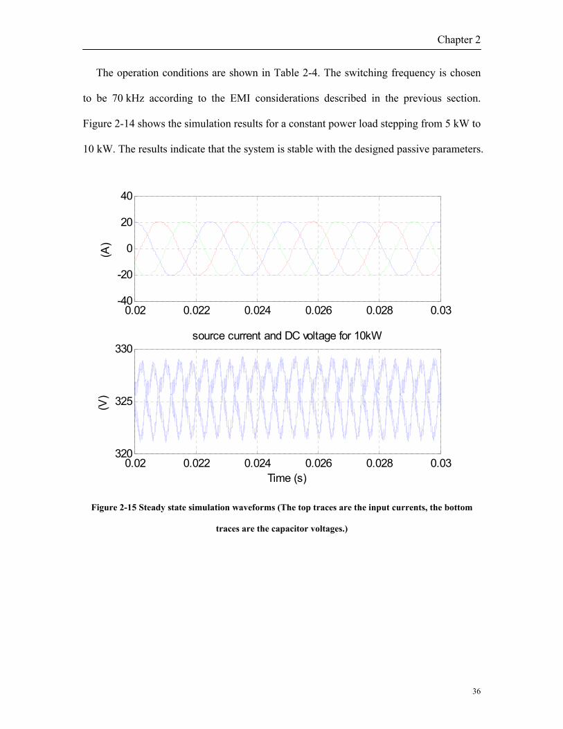
Chapter 2
36
The operation conditions are shown in Table 2-4. The switching frequency is chosen
to be 70 kHz according to the EMI considerations described in the previous section.
Figure 2-14 shows the simulation results for a constant power load stepping from 5 kW to
10 kW. The results indicate that the system is stable with the designed passive parameters.
0.02 0.022 0.024 0.026 0.028 0.03-40
-20
0
20
40
(A)
0.02 0.022 0.024 0.026 0.028 0.03320
325
330source current and DC voltage for 10kW
Time (s)
(V)
Figure 2-15 Steady state simulation waveforms (The top traces are the input currents, the bottom
traces are the capacitor voltages.)

Chapter 2
37
Figure 2-16 Harmonic current spectrum
Figure 2-17 EMI spectrum
105 106-40
-20
0
20
40
60
80
100Phase current EMI spectrum
(dB
uA)
Frequency (Hz)
SpectrumEMI Standard
0 2000 4000 6000 8000 10000 12000 14000 160000
0.1
0.2
0.3
0.4
0.5
0.6
0.7
0.8
0.9Current spectrum of 10kW case
Frequency (Hz)
(A)
SpectrumPQ Standard

Chapter 2
38
The full power steady state waveform is shown in Figure 2-15. The harmonic
spectrum analysis results of the input current as well as the power quality standard are
shown in Figure 2-16. The EMI spectrum analysis results and the standard requirement
are shown in Figure 2-17. The simulation results show that the converter designed
parameters meet the standard.
2.3 Summary
The design considerations and procedures to minimize the passive components of the
back-to-back VSC converter system are discussed and developed in this chapter. The
impact of the switching frequency on the filter corner frequency is studied by the
spectrum analysis. It shows that the relationship is non-monotonous. Higher switching
frequency will not necessarily lead to smaller EMI filter. Some preferred operating points
are determined. Then the lower bound for the line inductance is derived with the current
ripple requirement under a given switching frequency. The concept of using the same
inductor for boost function and EMI suppression is introduced in the design. Energy
storage and impedance interaction requirement are set up to determine the minimum DC
link capacitor. The current stress on the DC link cap and the failure mode impact are also
discussed. With the principles developed in this chapter, component parameters and
switching frequency selection can be traded off in order to achieve minimum passives.
The design approach is verified by simulation.

Chapter 3
39
Chapter 3 Topology Evaluation
This chapter presents a methodology to evaluate the three-phase ac topologies with the
metric of minimum weight [48]. The approach for passive filter selection developed in
Chapter 2 is applied when comparing different topologies. All major components and
subsystems in a converter are considered and the interdependence of all the constraints
and design parameters is systematically studied. The key design parameters, including
switching frequency, modulation scheme, and passive values, are selected considering
their impacts on loss, harmonics, electromagnetic interference (EMI), control dynamics
and stability, and protection. In this chapter four popular topologies are compared with
the proposed methodology.
3.1 Introduction
The power stage design clearly depends on the converter circuit topology. Therefore to
achieve a high-density design, it is a logical and necessary step to carry out the systematic
design and evaluation for the topologies that meet the application requirements, and
select among them the most suitable candidate.
For three-phase ac-ac converters, such as industrial motor drives, the two-level PWM
voltage source inverters with 6-pulse diode front-end rectifier has become the topology of
choice, due to its simplicity and relatively low cost. One drawback of the diode front-end
topology is the low order, low frequency harmonics on the dc link and ac input line,
which consequently requires bulky dc-link capacitor and inductor (ac or dc) filters. In
order to improve converter performance and achieve higher power density, many

Chapter 3
40
topologies for three-phase ac-ac converters or motor drives with active front-end
rectifiers have been proposed and studied [49-57]. These topologies can generally operate
with reduced passive components and improved input current wave form. On the other
hand, they may have increased loss and electromagnetic interference (EMI) noise,
requiring additional cooling and filtering [38]. Different active front-end topologies have
different loss, harmonics, and EMI characteristics, which often have contradictory impact
on the size and performance of the converter. To achieve a high power density design for
a specific application, comprehensive analysis and evaluation are needed to obtain an
optimal converter topology selection.
There has been considerable work on ac converter topologies evaluation. The previous
work generally focused on specific aspects of the converter design. For instance, [58]
compared the steady-state current and voltage waveforms as well as the harmonics
injected to the grid for two inverter topologies; [16] discussed device losses, input filter
and cost for three-level voltage source converters; [13] [14] [59] evaluated different
converter systems in terms of the grid-side power quality and loss distribution; [15]
compared the efficiency of the current source and the voltage source drive systems.
However, when developing a new converter for high-density applications, all aspects
contributing to the converter size and weight must be examined in the design, which
requires the correlation between all major design parameters be clearly established. There
is a clear need then for a systematic evaluation methodology considering the strong
interdependence of all design variables and constraints. For example, increasing
switching frequency generally helps to reduce the passive size, but it also increases the
converter switching loss and therefore heatsink size. As will be shown later in the chapter,

Chapter 3
41
even the relationship between the filter size and switching frequency is not monotonous,
as a result of changing loss characteristics and attenuation requirements of harmonic and
EMI standards. Generally speaking, operation conditions and constraints have great
influence on the component and converter size and weight. The constraints can be
physical ones as well as performance and system related. The examples of physical
constraints are: maximum junction temperature for devices, acceptable temperature rise
for magnetic and dielectric components, and voltage and current stress limits; the
examples of performance and system related constraints include: power ratings, power
quality and EMI requirements, etc. The auxiliary circuits, such as inrush current control,
protection and sensors, can also impact converter size and vary for different topologies,
and therefore should be considered in the topology evaluation as well. Finally the
selection of semiconductor devices, components, materials, and packaging also affect the
topology choice.
This chapter presents a systematic evaluation methodology of ac-ac converter
topologies for high density applications with emphasis on topologies with active front-
end rectifiers. The evaluation approach and selection criteria are first developed and
described in section 3.2. The evaluation examines all aspects of the design that contribute
to the size and weight of the converter, including: control, switching frequency,
semiconductor device loss and cooling, harmonic and EMI filters, and component design
and selection. The conclusions developed in chapter 2, including the parameters selection
criteria and switching frequency impact, are utilized in the evaluation. Following the
evaluation approach, a comparison study is carried out for four exemplary active front-
end topologies: back-to-back voltage source converters (BTB-VSC) [49], non-

Chapter 3
42
regenerative three-level boost (or Vienna-type) rectifier plus voltage source inverter
(NTR-VSI) [50-52], back-to-back current source converters (BTB-CSC) [53-54], and 12-
switch matrix converter [55-57]. Not only are these four well-known topologies for three-
phase ac-ac converters, but they also represent a broad category of implementations (two-
level, three-level, voltage-source, current-source, matrix, etc.). For each topology, a least-
weight design is sought under the same design conditions. The state-of-the-art SiC
devices are assumed in this study.
A main objective of this chapter is to provide a useful tool for practicing engineers for
selecting a high density topology for a given application. While the methodology applies
to both size and weight, the focus will be on the lowest weight design in the comparison
study, owing to the complexity involving system layout in determining the volume of a
converter.
Figure 3-1 Key components for an ac-ac converter
3.2 Evaluation Approach
Figure 3-1 shows a generic three-phase ac-ac converter diagram with active front-end.
All key size and weight contributors are shown, including input filter, dc link (filter and
auxiliary circuits), output filter, switching devices and heatsink, and need to be

Chapter 3
43
considered in the high-density design. It should be noted that not all of these elements are
needed for all topologies, or for all applications. The basic evaluation and comparison
approach is formulated similarly to a design optimization problem [60]. Design
conditions and constraints are first identified, including: performance constraints, such as
power quality and EMI standards; physical conditions and constraints, such as ambient
temperature, maximum device junction temperature and passive component thermal and
electrical limits. With a given design objective (in this case, size or weight), key design
parameters can then be varied and determined, including: switching frequency,
control/modulation strategy, minimum L and C values for both energy storage and filter
passives, device losses and cooling system thermal impedances.
Figure 3-2 Topology evaluation procedure

Chapter 3
44
The flowchart in Figure 3-2 shows the evaluation procedure for a low weight topology
selection: (1) First, the type of devices are specified, whether it is IGBT, MOSFET, GTO,
or SiC switches; (2) For a candidate topology, the semiconductor devices with proper
datasheet rating are preliminarily selected according to the operation conditions, such as
operating voltage and current; (3) Select the control and modulation scheme, which
impacts passive and thermal design; (4) Choose a preferred switching frequency within a
feasible range that is determined by the device characteristics. The “preferred” switching
frequency concept will be explained later in this section; (5) With chosen modulation and
switching frequency, the harmonic and EMI noise spectrum can be determined as
functions of passive components, based on which minimum L and C parameters are
designed to meet the system standards. In parallel, the device loss can be determined; (6)
Carry out physical design and selection for inductors and capacitors for the least weight,
and carry out thermal analysis and design for heatsink with given temperature conditions
and the thermal impedances; (7) Evaluate the total weight of the converter, including the
passives, heatsink, semiconductor devices, and the auxiliary circuit. Note that iterations
should be expected in the design process, such as selection of a different modulator,
varying the switching frequency, and adjustment of device rating selection as a result of
thermal design. For clarity, the iteration processes are omitted in Figure 3-2 flowchart.
All candidate topologies can be evaluated and compared with the same procedure. Some
of the key steps of the evaluation approach are described in details in this section below.
A. Modulation Scheme
Ac active converters are PWM controlled. Modulation schemes affect switching loss,
as well as voltage and current ripple spectrum, therefore the filter design. Modulation

Chapter 3
45
schemes are topology dependent. In general, there are no clear “optimal” modulators
since some are better for loss, while others may be better for ripple, or for dynamics.
Selection of the modulator is a key design choice. At least, two types of modulation
schemes should be evaluated in high-density design, the continuous PWM scheme, which
usually generates lower ripple, and the discontinuous PWM, which results in lower loss.
For some topologies, the modulator has extra functions, which have to be considered, e.g.,
the modulator of a multi-level converter often performs dc-link neutral-point control.
B. Preferred Switching Frequency
Switching frequency is a key design parameter. In general, increasing switching
frequency is an effective way to reduce passive components and increase power density,
until the increased loss in switching devices and in passive components outweighs the
benefit of the increased frequency. Therefore, for a specific application, there can be an
“optimal” switching frequency, which depends on the system, modulator, and
components. In principle, the switching frequency selection could involve search for the
optimal frequency. The conclusions from Chapter 2 can be utilized.
C. Loss Calculation and Heatsink Design
With selected modulation scheme and switching frequency, the power stage design
can be carried out, particularly, design of the major weight/size contributors of heatsink
and passives. The key to the heatsink design is power semiconductor device losses, which
are highly dependent on the device characteristics. There are many device
characterization methods. For topology evaluation study, it is appropriate to use a linear
approximation device model in (3-1) to (3-4) for the loss calculation. The conduction
voltage drop of the devices is given by (3-1) and (3-2), where VfT and Ron are the

Chapter 3
46
threshold forward voltage and the on-resistance of the switching device, VfD and RD are
the forward voltage and the on-resistance of the diode, vT , iT and vD , iD are the voltages
and currents of switch and diode respectively. The switching loss energy eT_on(off) and
eD_rev for switch and diode at operating point v(t) and i(t) can be modeled in (3-3) and (3-
4), where eT_on(off)_r and eD_rev_r are the switching energy and the reverse-recovery energy
at the measured operating point vr and ir, which can be obtained from either the datasheet
or experiments. Note that the device parameters VfT, Ron, VfD, RD, eon(off)_r and erev_r are all
significant functions of junction temperature. For the evaluation, the appropriate
temperature should be assumed, usually corresponding to the peak junction temperature.
On-state voltage drop of switch: TonfTT iRVv ⋅+= (3-1)
On-state voltage drop of diode: DDfDD iRVv ⋅+= (3-2)
Switching energy of switch: rr
roffonToffonT ivtitvee
⋅⋅
⋅=)()(
_)(_)(_ (3-3)
Switching energy of diode: rr
rrevDrevD ivtitvee
⋅⋅
⋅=)()(
___ (3-4)
Given the semiconductor devices and operating conditions, the power loss for any
given topology and modulation scheme can be found with (3-1) to (3-6). Examples of
loss calculations will be given for selected topologies and devices in Section III.
+−
jT hT
cQ
0T
Figure 3-3 Device thermal structure illustration Figure 3-4 Thermal equivalent model

Chapter 3
47
Knowing the loss, the thermal calculation can be performed. For topology evaluation,
one dimensional equivalent thermal model, consisting of equivalent thermal impedances
of device package, heatsink, and other thermal interface materials, should be sufficient.
Figure 3-3 shows an example of the thermal interface structure and Figure 3-4 shows the
corresponding one dimensional steady-state thermal equivalent circuit, where Qc is the
power loss generated by the device, R1 is the thermal resistance from junction to case, R2
represents the thermal resistance of thermal interface between the case and the heatsink,
R3 is the thermal resistance of the heatsink to the ambient. Tj, Th, and T0 are temperatures
of the semiconductor device junction, heatsink and ambient respectively. The thermal
resistances can be obtained from datasheet, measurements, or simulation. If there is
transient overload, thermal capacitances should also be considered. In the case without
transient overload, the junction temperature of the k-th device can be obtained as in (3-5),
where Tj_k and Qc_k correspond to the junction temperature and power losses for the k-th
device, Tlimit is the upper limit for the operating junction temperature for that device (e.g.
125°C for many commercial Si devices).
ithkckj TTRRQT lim21__ )( ≤++⋅= (3-5)
With (3-5), the acceptable upper limit of the heatsink temperature corresponding to
that particular device may be readily found. For an ac converter with multiple devices,
this value could vary with device and the lowest one should be chosen as the upper
temperature limit for the whole heatsink. Then the required thermal resistance for the
heatsink is given in (3-6). With a given ambient temperature and cooling
method/conditions, heatsink can be selected or designed to meet the requirement of (3-6)
and the corresponding size and weight of the cooling system can be determined.

Chapter 3
48
ch QTTR /)( 03 −= (3-6)
D. Passive Component Parameter Minimization and Physical Design
Depending on topologies, the passives in an ac-ac converter can include dc-link
capacitor and/or dc-link inductor, ac input line inductor or capacitor, as well as input
and/or output filter for suppressing harmonics, EMI, and dv/dt. The output filters are
generally application dependent and will not be considered in this work. The approach
used here should be applicable to output filters for specific applications.
Energy storage capacitance and inductance minimization: For energy storage passives,
i.e., dc-link and ac-line capacitors and inductors, minimum parameters should first be
determined according to a number of performance and system requirements. The
parameter selection is topology dependent. In general, for the dc-link capacitor (for
voltage source topology) or inductor (for current source topology), their selection needs
to consider the following requirements:
1) Energy storage: The dc-link voltage variation (for voltage source topology) or
current variation (for current source topology) caused by the instantaneous
energy unbalance should be limited to an acceptable level. The energy
unbalance can be caused by a sudden change in load or source conditions.
2) Stability: Impedance characteristics of the dc link determine the stability of
the converter system [46].
For boost inductor (for boost topology) and capacitor (for buck topology), their
selection need to consider:
1) Harmonics: often in terms of total harmonic distortion (THD).

Chapter 3
49
2) Peak ripple current: The peak ripple current as results of switching will impact
the inductor flux, and therefore the inductor sizes.
3) Inrush: High current peaks will occur in voltage source topologies during start
up or recovery from a voltage drop, which will impact both the inductor
design and the capacitor selection.
Figure 3-5 CL-CL filter for CSC
Filter Passive Minimization: The ac input filters should also be designed to meet EMI
standards requirements. For comparison discussion, this section uses a two-stage LC-LC
filter for voltage source topologies, as shown in Figure 2-7, and a CL-CL filter for current
source topologies, as shown in Figure 3-5. The design objective is to minimize the L and
C values while complying with the EMI standard. The design approach was discussed in
Chapter 2. While damping design for high frequency resonance is an integral part of filter
design, it is omitted here since damping components contribute little to weight and size
and they can be common for all topologies. Both passive [20] and active [61] [62]
damping schemes can be used. Note that the EMI filter passives and energy storage
passives can be combined or integrated in the design for further reduction of size and

Chapter 3
50
weight, which means that the input filter can be designed as one entity to achieve
harmonic and EMI filtering functions as well as for energy storage. Examples of such
design will be shown in Section 3.3.
Capacitor Design and Selection: In most practical converter designs, the capacitors
are selected based on available commercial parts. For high density and light weight
design, the smallest and lightest capacitors should be selected that also meet the
capacitance, voltage, current, and thermal requirements. Commercial film capacitors are
selected in this work for comparison purposes. The section examples are demonstrated in
Section 3.3.
Inductor Design: Toroid cores are assumed for the CM choke, and EE cores for the
ac-line and dc-link inductors. The design constraints are: required inductance and
physical limits such as saturation, window area, insulation and maximum temperature
rise [63]. The leakage inductance of the CM choke [64] is also considered as a design
constraint in order to achieve the required DM attenuation. In this work ferrite (R
material) from Magnetics are used for the ac-line and dc-link inductor design, and
nanocrystalline (FT-3M) material for the CM choke design. The core losses under
sinusoidal excitation are given by (3-7) [65] and (3-8) [66], where the core loss is in W, f
is the frequency in kHz, dB is the peak flux density change in kGauss, and Vcore is the core
volume in cm3. Based on (3-7) and (3-8) the improved Generalized Steinmetz Equation
[67] can be used to calculate the core loss of the inductors.
Loss of ferrite (R material): 104.7 85.243.15corecore VdBfP ⋅⋅⋅×= − (3-7)
Loss of nanocrystalline (FT-3M material): corecore VdBfP ⋅⋅⋅×= − 982.1621.151034.8 (3-8)

Chapter 3
51
b a
c
Figure 3-6 Design variables for the EE core Figure 3-7 Design variables for the toroid core
An optimization function (FMINCON) in Matlab is used to determine the physical
dimensions to achieve minimum weight. The design variables are the core dimensions (as
shown in Figure 3-6 and Figure 3-7), air gap and the number of turns. All the designed
constraints mentioned above are considered and the total weight is the objective function
for both inductors. Based on this algorithm the optimal inductor design and the
corresponding weight can be obtained under the given operating conditions and the
designed inductance value.
E. Auxiliary Circuits, Design Variation and Iteration
In addition to cooling and passive components, the other relatively important
topology-dependent weight contributors include power device packages and auxiliary
circuits, such as inrush control and protection circuits. Together, the total weight of the
converter can be determined and compared with the result of a different design or
topology.
Clearly, for each given topology, there can be different designs with different
converter weights, while all meeting the performance requirements and design constraints.
In principle, every key parameter can have its design range. In practice, design variation
and iteration should be performed to achieve the least weight design. For example, there

Chapter 3
52
are several preferred switching frequencies observed in Figure 2-6, and the most suitable
one needs to be selected through design iteration. The device rating selection should be
traded off with losses, thermal impedance, and heatsink. The design variation can be
systematically carried out following the flowchart process in Figure 3-2 and even
automated with computer programming or optimization.
3.3 Topology Comparison
Based on the proposed approach, four three-phase ac-ac active front-end topologies as
shown in Figure 3-8 are evaluated and compared. While these candidate topologies cover
a range of circuits often used in high-density converter design and study, their selection is
not meant to be exhaustive and is intended only to demonstrate the effectiveness of the
evaluation procedure, which should also be applicable to other topologies. Table 3-1 lists
the sample system specifications and requirements used in this comparison study. SiC
devices are selected in the comparison since they offer the advantages of low loss, high
switching frequency and high operating temperature [68]. The commercial SiC diode
C2D20120 (1200V/20A) and a 1200V/5A JFET from SiCED are selected in this study.
The diode parameters are available from datasheet. At 175°C, the JFET has an on-
resistance of 0.8 Ω and a switching energy of 155 µJ (at 400V/10A) [69]. The number of
paralleling devices required varies with the topologies according to the current and
thermal requirement. For comparison purpose, all candidate topologies keep the same
total number of devices (a total of 72 devices including the diodes and JFETs).

Chapter 3
53
Figure 3-8 (a) Back-to-back VSC, (b) Non-generative three-level boost rectifier plus voltage source
inverter, (c) Back-to-back CSC and (d) 12-switch matrix converter
As explained in Section 3.2, switching frequency is a key design parameter. There are
preferred switching frequencies for the front-end rectifier based on input EMI filter
requirements. In principle, for the inverter, the switching frequency can be separately
selected based on output filter requirement and the load specs. Since the output filter is
very application dependent and therefore omitted in this work, the inverter switching
frequency is chosen to be the same as the rectifier for comparison purpose. In the
comparison study, four switching frequencies are used, 40 kHz, 70 kHz, 100 kHz, and
140 kHz, and the corresponding designs are obtained and compared. From Figure 2-6, it
can be seen that fsw<40 kHz can result in higher corner frequency for EMI filter. The low
switching frequency boundary is selected to be 40 kHz to avoid relatively low-order
harmonics, given the 400-800 Hz fundamental frequency range. For a different design
spec, a lower or higher switching frequency range may be selected.
MAC
AC
AC
LinCdc M
AC
AC
AC
Lin C1
C2
M
AC
AC
AC
Cin
Lin
(a) (b)
(c) (d)
M
AC
AC
AC
Lin
Cin
Ldc
Cout

Chapter 3
54
Table 3-1 System Specifications
Input Voltage 230 Vrms Dc-link Voltage (for VSC) 650 V
Power 10 kW Dc-link Current (for CSC) 25 A
Devices 1200V SiC JFET, SiC Schottky Diode
Line Frequency 400-800 Hz Junction Temperature 175°C
Ambient Temp. 70°C Air Flow 2 m/s
Standard Requirement RTCA/DO-160E
0.025 0.026 0.027 0.028 0.029 0.03-50
0
50
(a)
0.025 0.026 0.027 0.028 0.029 0.03-1000
0
1000
(b)
Figure 3-9 Simulation results for BTB-VSC: (a) ac-line currents; (b) PWM line-to-line voltage
A. BTB-VSC
BTB-VSC, as shown in Figure 3-8 (a), is a popular topology in many applications. 60°
DPWM is implemented in this work for better EMI noise performance and lower
semiconductor loss compared to continuous PWM [42]. In Figure 3-9 the simulation
waveforms of ac-line currents and PWM line-to-line voltage are shown (Circuit
parameters: Lin = 100 μH, Cdc=10 μF, fSW=40 kHz).

Chapter 3
55
Based on the conclusions in Chapter 2, we can determine the required passive filter
parameters. For comparison purpose, the capacitor Cx and Cy are selected to be 1 µF and
6.8 nF respectively for all the topologies and then the inductances vary to meet the corner
frequency. For the 40 kHz case, the common mode and differential mode inductances are
10 mH and 110 µH respectively. Since the ac-line inductor can also be a part of the EMI
filter. So the total input inductance should be the larger one between the two values
designed for the DM inductor and the line inductor respectively. In this case the EMI
filter DM inductance is dominant, which can be the leakage inductance of the CM choke.
Based on the designed parameters and operating conditions, the optimization algorithm
shown in the previous section is used to design the actual inductor (physical unit). The
dc-link capacitance is selected to be 10 µF for 40 kHz switching frequency. Four 400 V /
10 µF film capacitors are chosen in the design to form the equivalent 10 µF dc-link
capacitor bank to meet the voltage and the ripple current requirement.
refvv
tω 1Vv
2Vv
0Vv
11 Vdv
⋅
22 Vdv
⋅
Figure 3-10 Vector synthesis in sector I of space
vector diagram
Figure 3-11 Pulse pattern for the top switches in
the first 30°
Cooling System: For loss calculation in topology evaluation, the dc-link voltage ripple
and ac input/output current harmonics can be neglected. Under the assumption, the
current through each device is only determined by the switching pattern and the duty

Chapter 3
56
cycle. With the three-phase symmetrical system, for the loss calculation, we can just
consider the losses in one sixth of the line cycle. Figure 3-10 shows the voltage vector
synthesis in sector I of the space vector diagram [42]. The duty cycles d1, d2, and d0 for
voltage vectors 1Vr
, 2Vr
and 0Vr
are given by (3-9). Figure 3-11 shows the pulse patterns of
the top switches for the first 30° in sector I. With (3-9) the duty cycles for phase-legs are
given by (3-10).
⎪⎪⎪⎪
⎩
⎪⎪⎪⎪
⎨
⎧
−−=
=
−=
210
2
1
1
sin23
)3
sin(23
ddd
tMd
tMd
ω
ωπ
(3-9)
⎪⎪⎪
⎩
⎪⎪⎪
⎨
⎧
−⋅−==
+⋅−=+=
=
)6
cos(231
)6
cos(231
1
0
02
πω
πω
tMdd
tMddd
d
c
b
a
(3-10)
The switching loss of SiC diodes is ignored as they have excellent reverse recovery
performance [70]. With the linear assumption the power losses of the SiC JFET and
diode in the phase-leg of the rectifier at the j-th switching cycle are given by (3-11) and
(17), where Ir(t) is the instantaneous rectifier input current, dr(t) is the instantaneous duty
cycle of the corresponding phase-leg of the rectifier given by (3-10), Vdc is the dc-link
voltage, Nr_T and Nr_D are the numbers of parallel JFETs and diodes in the rectifier
respectively. Nr_T=4 and Nr_D=2 for the BTB-VSC.
( )sw
rr
rdcroffonTr
Tr
onrjJFETr f
ivtIV
etINR
tdP ⋅⋅⋅
⋅+⋅⋅−= _)(_2
___ )())(1( (3-11)
])()([)( 2
___ tI
NRtIVtdP r
Dr
DrfDrjDior ⋅+⋅⋅= (3-12)

Chapter 3
57
The power losses in the inverter are given by (3-13) and (3-14), where Ii(t) is the
instantaneous inverter output current, di(t) is the instantaneous duty cycle of the
corresponding phase-leg of the inverter, Ni_T and Ni_D are the numbers of parallel JFETs
and diodes an inverter phase-leg respectively. Ni_T=5 and Ni_D=1 in this case.
( )sw
rr
idcroffonTi
Ti
onijJFETi f
ivtIV
etINR
tdP ⋅⋅⋅
⋅+⋅⋅= _)(_2
___ )()( (3-13)
])()([))(1( 2
___ tI
NRtIVtdP i
Di
DifDijDioi ⋅+⋅⋅−= (3-14)
Assume sinusoidal Ir(t) and Ii(t), equations (3-11) to (3-14) are used to calculate the
average losses of the semiconductor devices on the phase-leg. The same procedure is
used to obtain the losses of the other phase-legs and the sum of the phase-leg losses
yields the total converter loss. And then with (3-5) and (3-6) the required thermal
impedance for the heatsink can be determined. The aluminum heatsink OS080 from
Aavid Thermalloy is selected in this work. The width and the height are 135 mm and 25
mm respectively. The length of the heatsink varies with the required thermal resistance.
Two fans (614F series from ebm-papst Inc.) are assumed for all the topologies. The
weights of the inductors are calculated by the designed core dimensions and the number
of winding turns with the material density. The weights of the other components are
obtained from the data sheet. The loss calculation results and the weight distribution for
the BTB-VSC are shown in Table 3-2.
B. NTR-VSI
The topology is shown in Figure 3-8 (b). In comparison to the BTB-VSC, the two-
level active front-end is replaced in this case by a non-regenerative three-level boost
rectifier, which offers the advantages of lower voltage stress to the devices and lower

Chapter 3
58
harmonic distortion. But it does not provide the regenerative capability. Three-level
continuous space vector PWM is used for the rectifier [71] and DPWM is implemented
for the VSI as the BTB-VSC. Figure 3-12 shows the simulation waveforms (Lin = 100 μH,
C1=C2=20 μF, fSW=40 kHz). The spectrum analysis for the PWM voltage is shown in
Figure 3-13 for 40 kHz switching frequency. Since the non-regenerative three-level
rectifier is a voltage source rectifier, the input filter design and the dc-link capacitor
selection can follow the same approach as the BTB-VSC. For the 40 kHz case, the
common mode and differential mode inductances are 7.8 mH and 97 µH respectively.
The dc-link capacitors are 20 µF each so that the total dc-link capacitance is 10 µF.
0.025 0.026 0.027 0.028 0.029 0.03-50
0
50
(a)
0.025 0.026 0.027 0.028 0.029 0.03-1000
0
1000
(b)
Figure 3-12 Simulation results for NTR-VSI: (a) ac-line currents; (b) PWM line-to-line voltage

Chapter 3
59
0 0.5 1 1.5 2
x 105
0
50
100
150
200
250
300
350
Frequency (Hz)
Am
plitu
de o
f har
mon
ics
(V)
Figure 3-13 Spectrum of the PWM voltage for NTR-VSI
For the rectifier, the power losses of the JFET and the main bridge diode have the
same expressions as (16) and (17) except that 0.5Vdc should be utilized instead of Vdc for
the JFET switching energy calculation in (16). The loss of the neutral bridge diode is
given by (20), where Nr_Dn is the number of parallel diodes in the neutral bridge. Nr_T,
Nr_D and Nr_Dn are 4, 2 and 1 respectively in the design.
])()([))(1(2 2
____ tI
NRtIVtdP r
Dnr
DfDrjneuDior ⋅+⋅⋅−⋅= (3-15)
The VSI is modulated using DPWM and therefore its losses are determined by (3-13)
and (3-14). Similar to the BTB-VSC the heatsink design is then carried out based on the
loss calculation. Table 3-3 shows the design results for NTR-VSI.
C. BTB-CSC
Figure 3-8 (c) shows the topology of BTB-CSC. The energy storage component in the
dc link is an inductor instead of a capacitor. Both input and output filters are required to
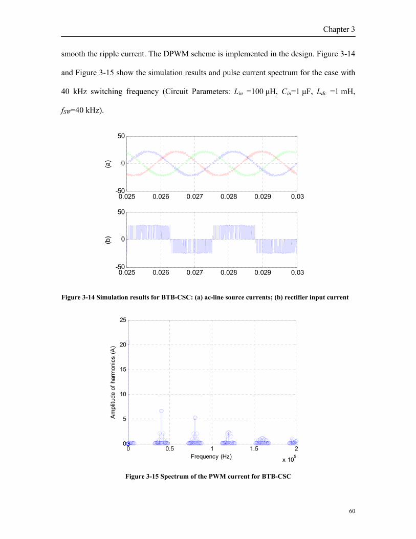
Chapter 3
60
smooth the ripple current. The DPWM scheme is implemented in the design. Figure 3-14
and Figure 3-15 show the simulation results and pulse current spectrum for the case with
40 kHz switching frequency (Circuit Parameters: Lin =100 μH, Cin=1 μF, Ldc =1 mH,
fSW=40 kHz).
0.025 0.026 0.027 0.028 0.029 0.03-50
0
50
(a)
0.025 0.026 0.027 0.028 0.029 0.03-50
0
50
(b)
Figure 3-14 Simulation results for BTB-CSC: (a) ac-line source currents; (b) rectifier input current
0 0.5 1 1.5 2
x 105
0
5
10
15
20
25
Frequency (Hz)
Am
plitu
de o
f har
mon
ics
(A)
Figure 3-15 Spectrum of the PWM current for BTB-CSC

Chapter 3
61
For the filter design, the same procedure as BTB-VSC is followed while the Fourier
analysis is carried out for the pulsating current instead of the voltage at the rectifier input
terminal. As mentioned in Section II, a CL-CL input filter is used for this topology. For
the 40 kHz switching frequency case, the required inductance is 162 µH with 1 µF
capacitance. This dc-link inductor should also meet the stability and energy storage
requirements, expressed by (3-16) and (3-17), where Idc is the dc-link current, and ΔI is
the maximum ripple current (7 A in the example design).
)21( 2
max
IIIf
PL
dcsw Δ±Δ≥ (3-16)
mdc
outBW Z
IP
Lf ≥− )lg(20)2lg(20 2π (3-17)
With the above two equations the dc-link inductor is designed to be 1.27 mH for
40 kHz switching frequency case with 6 dB impedance margin and 4 kHz control
bandwidth. In BTB-CSC the output capacitors are usually required to smooth the output
waveform, especially for the motor load. In this work the voltage THD requirement is
used to determine the output capacitance. Assuming all ripple components of the output
current go through the output capacitors, the relationship between the output capacitance
and the voltage THD can be achieved with the spectrum analysis result for the output
current. For a 30% THD requirement, the capacitance is designed to be 1 µF when the
switching frequency is 40 kHz.
For BTB-CSC the losses of the power devices have the same expressions for the
rectifier and inverter, which are given by (3-18) and (3-19), where d(t) is the
instantaneous duty cycle, VL(t) is the instantaneous line-to-line voltage, NT and ND are the
numbers of parallel JFETs and diodes respectively. NT =5 and ND =1 for this case. With

Chapter 3
62
(3-18) and (3-19) the losses of each individual device and the total system can be
achieved and then heatsink can be readily designed. The design results for the B2B-CSC
are shown in Table 3-4.
swrr
dcLroffonTdc
T
onjJFET f
ivItVeI
NRtdP ⋅
⋅⋅
⋅+⋅⋅=)()( _)(_
2__ (3-18)
)()( 2__ dc
D
DdcfDjDio I
NRIVtdP ⋅+⋅⋅= (3-19)
D. 12-Switch Matrix Converter
The 12-switch matrix converter, as shown in Figure 3-8 (d), consists of a cascaded
connection of two bridge converters without any dc-link energy storage components. The
converter at the input terminal has the same structure as the front-end rectifier of the
BTB-CSC, which is treated as the current source bridge (CSB); and the converter at the
output terminal is treated as the voltage source bridge (VSB) since it has the same
structure as the inverter of BTB-VSC.
A carrier based modulation scheme [72] is implemented and the corresponding noise
spectrum is used for the filter parameters design. The simulation results and the spectrum
analysis for the phase-leg pulsating current for 40 kHz switching frequency case are
shown in Figure 3-16 and Figure 3-17 respectively (Lin = 100 μH, Cin= 4 μF, fSW=40 kHz).
Since the pulsating current is the noise source in the 12-switch matrix converter, the CL-
CL structure is chosen for the input filter and the design follows the same way as the
BTB-CSC. For the case of 40 kHz switching frequency, the inductance is 128 µH with
the capacitance selected to be 1 µF.

Chapter 3
63
0.025 0.026 0.027 0.028 0.029 0.03-50
0
50
(a)
0.025 0.026 0.027 0.028 0.029 0.03-50
0
50
(b)
Figure 3-16 Simulation results for 12-switch matrix converter: (a) source currents; (b) PWM line
current
0 0.5 1 1.5 2
x 105
0
5
10
15
20
25
Frequency (Hz)
Am
plitu
de o
f har
mon
ics
(A)
Figure 3-17 Spectrum of the PWM current for matrix converter
Losses are determined in the following way: for CSB, the switching loss is zero under
the modulations scheme used, and the conduction losses are given in (3-20) [73], where I0
is the amplitude of the output current, M0 is the modulation index, and 0φ is the output

Chapter 3
64
power factor angle, which is assumed to be 0° for all the sample designs. The numbers of
parallel JFETs Nr_T and diodes Nr_D in CSB are 5 and 1 respectively for the sample design.
))cos(41()(2
33)cos(29 2
02
00__
2000_ φπ
φπ
⋅+⋅⋅⋅+⋅+⋅⋅⋅⋅= IMN
RNR
IMVPDr
D
Tr
onfDCSBc (3-20)
For VSB, the conduction and switching losses are given in (3-21) and (3-22) by [73],
where Vs is the amplitude of the input phase voltage and iφ is the input power factor
angle (0° for the sample designs). The numbers of JFETs Ni_T and diodes Ni_D in VSB are
5 and 1 respectively.
⎥⎥⎥⎥⎥
⎦
⎤
⎢⎢⎢⎢⎢
⎣
⎡
⋅⋅⋅−+⋅⋅⋅⋅
−⋅++⋅
=
)cos()()cos(83
8)(
26
002
20
__000
20
__
0
_
φπ
φπ
π
MINR
NRMIV
INR
NRIV
P
Di
fD
Ti
onfD
Di
fD
Ti
onfD
VSBc (3-21)
)cos(27 0_)(_2_ i
rr
sroffonTswVSBsw iv
IVefP φπ
⋅⋅⋅
⋅⋅⋅= (3-22)
With (25-27), the losses for the devices can be obtained and then the heatsink can be
selected. Table 3-5 shows the design results for the 12-switch matrix converter.
E. Topology Comparison Results and Discussions
Figure 3-18 shows the total weight comparison of the four different topologies under
consideration for four switching frequencies. From the results, it can be seen that the
BTB-CSC has the highest losses and also the heaviest passive components. The NTR-
VSI and the BTB-VSC present comparable weights, with the latter having slightly lower
loss, but slightly larger filter. The 12-switch matrix converter requires the least passives
but its higher loss makes it an inferior to the BTB-VSC and NTR-VSI topologies. It can
also be seen that 40 kHz switching frequency is the best choice for all topologies due to
the dominance of heatsink weight, except for BTB-CSC. It should be emphasized that

Chapter 3
65
these conclusions are based on specific design conditions and component characteristics.
For a different design, the same procedure can be applied and different conclusions on
topology selections may arise.
Figure 3-18 Weight comparison of four topologies under consideration
Table 3-2 Design Results for BTB-VSC
BTB-VSC f=40k f=70k f=100k f=140k
Loss (W) 206 238 268 309
Heatsink (g) 426 492 558 754
Power device (g) 432 432 432 432
Input filter (g) 576 676 912 614
DC Cap (g) 110 80 50 40
Fan (g) 50 50 50 50
Protection (g) 30 30 30 30
Total Weight (g) 1624 1760 2032 1920

Chapter 3
66
Table 3-3 Design Results for NTR-VSI
NTR-VSI f=40k f=70k f=100k f=140k
Loss (W) 236 267 297 338
Heatsink (g) 459 590 738 951
Power device (g) 432 432 432 432
Input filter (g) 498 432 502 358
DC Cap (g) 110 80 50 40
Fan (g) 50 50 50 50
Protection (g) 60 60 60 60
Total Weight (g) 1609 1644 1832 1891
As mentioned above, auxiliary circuits such as inrush control and protection circuits
also contribute to the converter weight and should be considered in topology evaluation.
They are topology dependent. Among the four studied topologies, BTB-VSC and NTR-
VSI require extra inrush control and dc-link over voltage protections [74]. Their
estimated weights are included in Tables 3-2 and 3-3. Since the weights are relatively
small, the detailed design descriptions are omitted here.
Note that in these Tables, the weights of the power devices are the same for all
topologies with the comparison condition that all topologies use the same number of
devices with the same packages. Because of the commercial package limitations for SiC
devices, the device weights constitute an unusually high percentage in the converters.
With better packaging, device weights should be significantly reduced. In this case, the
device weight does not change the comparison results of the topologies as a common
factor. The same cooling fan is also assumed in different designs due to its relatively
small size.

Chapter 3
67
Table 3-4 Design Results for BTB-CSC
BTB-CSC f=40k f=70k f=100k f=140k
Loss (W) 678 712 745 790
Heatsink (g) 2408 2685 3010 3565
Power device (g) 432 432 432 432
Input filter (g) 724 730 1010 756
DC Inductor (g) 1166 767 600 477
Output filter (g) 24 18 15 10
Fan (g) 50 50 50 50
Total Weight (g) 4804 4682 5117 5290
Table 3-5 Design Results for 12-Switch Matrix Converter
Matrix f=40k f=70k f=100k f=140k
Loss (W) 369 401 433 475
Heatsink (g) 902 1066 1230 1460
Power device (g) 504 504 504 504
Input filter (g) 604 548 674 510
Fan (g) 50 50 50 50
Total Weight (g) 2060 2168 2458 2524
Some interesting observations can be made based on the topology comparison results.
Matrix converter, which requires no dc-link capacitors, has often been considered a
natural choice for high-density design. In our case, the comparison clearly shows that the
matrix converter does not result in a lower weight design due to its higher loss and
corresponding larger heatsink. The BTB-CSC would be a good topology that suits well
with the normally-on characteristics of SiC JFET. Unfortunately, its high loss makes it

Chapter 3
68
the heaviest design among the four candidate topologies. These comparison results prove
the value of a systematic topology evaluation in high-density converter design.
Figure 3-19 Formulation of the converter optimization
As mentioned earlier, the presented topology evaluation approach is formulated
similarly to an optimization problem. The design conditions, constraints, and variables
are defined for achieving a high-density design. The focus of the work has been on
establishing the relationships between all these parameters and on determining the
preferred topology relative to the others. Although the presented designs may only be
preferred rather than optimal due to limited iterations, the approach provides insight on
correlations of all key parameters, which can be applied to any ac-ac converters. The
proposed approach and analysis can also form a basis for global optimization of an ac-ac
converter. Figure 3-19 shows the conceptual formulation of such an optimization. The

Chapter 3
69
key to the optimization is establishing the relationships, through models and equations,
between design conditions, constraints, variables, and objectives, which has been the
main focus of this work. The actual optimization can follow various standard algorithms
including generic algorithm [75], which is not covered in this dissertation.
3.4 Summary
A systematic evaluation approach of three-phase PWM ac-ac converter topologies for
high-density design has been developed in this chapter. All major components and
subsystems in a converter system are considered, including the switching devices,
heatsink, energy storage and filter passive components, and auxiliary circuits. A
comprehensive list of design conditions, constraints, and parameters, and their
interdependencies on converter density are considered. With the high frequency
capability SiC devices assumed, the impact of the switching frequency is carefully
studied considering loss, passive size, and EMI filter design, culminating with identifying
a non-monotonous relationship. The impact of modulation schemes on loss and passives
is also considered, and it is found that lower-loss modulation schemes do not necessarily
lead to bigger passives. The concept of using the same inductor for harmonic suppression
and EMI filtering is implemented in the design. In addition, auxiliary circuits such as
protection circuits can add to the total size and weight. Based on the proposed approach
four active front-end converters using SiC devices are quantitatively compared for lowest
weight design. The comparison results show that the BTB-VSI and NTR-VSI topologies
present lighter total weight for the given specifications than BTB-CSC or matrix

Chapter 3
70
converter. The proposed methodology can be extended to other topologies with different
comparison metrics and can be a useful tool for high-density topology selection.

Chapter 4
71
Chapter 4 Modeling and Control for Non-Regenerative
Three-Level Boost Rectifier
In the previous chapter the non-regenerative three-level boost (Vienna-type) rectifier
plus voltage source inverter is found to be the preferred topology from the system weight
standpoint. However the control for the Vienna-type rectifier is relatively complicated
due to the three-level structure. Good control approach is desired to guarantee the high
frequency operation in order to achieve the high density.
This chapter starts with the development of a new average d-q model for the Vienna-
type rectifier. An optimal zero sequence injection concept is found from the perspective
of dc-link voltage balance. With this average model a new control algorithm with carrier-
based PWM implementation is developed, which features great simplicity and good
neutral point regulation. The proposed control approach is verified by experiments.
4.1 Introduction
The non-regenerative three-level boost rectifier [76] [77] [78] is characterized by
reduced number of active switching devices, high input power factor and low device
voltage stress, which make it a suitable topology for medium and high power applications
[13] [79]. But its controller is relatively complex because of the current forced
commutation characteristics and the dc-link neutral point voltage regulation requirement.
In the past several years lots of research work has been put on the Vienna-type
rectifier, including the average model manipulation [80] [81] [82] and the control scheme
development [52] [71] [83] [84] [85]. The previous modeling efforts focused on the d-q

Chapter 4
72
representation for the rectifier system. However, due to the intrinsic time variant nature
of the dc-link neutral point current [50] it is difficult to directly achieve the equilibrium
point with the conventional d-q coordinate transformation. For this reason low frequency
state model [80] [81] [82] was built by averaging the dc-link neutral point operation in a
complete ac line cycle.
On the control side, several approaches have been proposed for this type of rectifier.
Hysteresis current control [83] is simple to implement as the switch gating signals are
generated by comparison of the reference and measured currents. The drawback of this
approach is that the frequency is not constant, which is not desirable for industrial
applications. Constant-frequency integration control [84] and unity power factor control
[52] feature both simplicity and constant switching frequency, but they do not provide
closed loop regulation capability for the dc-link neutral point voltage. Consequently in
order to limit the voltage unbalance of the dc link, bigger dc-link capacitors are needed.
Three-level space vector based control scheme [71] [85] provides a clear insight into the
system control and operation as the redundant vectors can be utilized to regulate the
neutral point voltage. However large calculation effort is required for the implementation,
which has limited its application in high switching frequency cases. And the control loop
design for the voltage balance is absent in the existent control approaches [52] [71] [84]
due to the limited frequency range of the available models.
In this chapter, a new average model for the Vienna-type rectifier with extended
frequency range is proposed based on the state space analysis and the concept of optimal
neutral point current injection. The state space model for the system is first built and the
relationship between the controlled duty cycle and the voltage unbalance is set up with

Chapter 4
73
the differential equation. Based on this correlation an optimal zero-sequence component
for the duty cycle is found to achieve zero current injection to the dc-link neutral point,
which implies an equilibrium point of dc-link voltage balance. By utilizing this optimal
zero component into the duty cycle the average model for the neutral point operation can
be greatly simplified, and a simple mathematical relationship between the voltage
unbalance and the controlled zero sequence duty cycle is found. Therefore the neutral
point voltage control loop can be easily designed.
Based on the proposed average model, a new control algorithm with carrier-based
implementation is presented, with which the full control function of the Vienna-type
rectifier is achieved by simply embedding the dc-link voltage balance control loop into
the conventional multi-loop d-q controller. Compared to the previous methods, the new
control approach features great simplicity and better dc-link voltage regulation. An
FPGA-DSP controlled rectifier prototype is built and the proposed model and control
approach are verified by the simulation and the experiment results.
The space vector representation is also utilized to analyze the voltage balance
mechanism of the neutral point as well as the feasible operation region. The analysis
shows that they are mathematically the same in terms of keeping the neutral point balance.
However, in the proposed approach the zero sequence duty cycle is partially generated by
a feed-forward method instead of the space vector modulator, which leads to a significant
reduction of the calculations.

Chapter 4
74
4.2 Average Model Derivation
The topology of a non-regenerative three-level boost rectifier is shown in Figure 4-1,
which comprises of a main diode bridge and the neutral point switch cells. As can be seen,
only one controlled switch is used for each phase leg. Since this type of rectifier is
current force commutated, the rectifier pole voltage (VAN, VBN, VCN) is determined by not
only the controlled switch state but also the polarity of the phase current at the
corresponding instant. For instance, if the switch Qa is off and the line current iA is
positive, the phase leg A is clamped to the positive dc link, therefore VAN is equal to Vdc/2.
Similarly, if Qa is off and iA is negative, VBN will be –Vdc/2. If the Qa is on, phase leg A
will be clamped to the midpoint of the dc link and VAN is zero, regardless of what the
current polarity it is. The same operation principle applies to phase B and phase C.
Figure 4-1 Rectifier topology
For the input stage, the state space equations are given by

Chapter 4
75
⎪⎪⎪
⎩
⎪⎪⎪
⎨
⎧
++=
++=
++=
NOCNC
cs
NOBNB
bs
NOANA
as
VVdt
diLV
VVdt
diLV
VVdt
diLV
. (4-1)
Since the Vienna-tupe rectifier is current force commutated, the switch voltage VAN,
VBN and VCN are determined by both the switching pattern and the current polarity, which
are given by
⎪⎪⎪⎪
⎩
⎪⎪⎪⎪
⎨
⎧
−⋅Δ
+⋅=
−⋅Δ
+⋅=
−⋅Δ
+⋅=
)1(])[sgn(2
)1(])[sgn(2
)1(])[sgn(2
cdc
Cdc
CN
bdc
Bdc
BN
adc
Adc
AN
Sv
vivV
Sv
vivV
Sv
vivV
. (4-2)
where vdc=vC1+vC2, ∆v=vC1-vC2, sgn is the sign function, Sa, Sb and Sc are the switching
function defined as
⎪⎩
⎪⎨⎧
=on turnedis Q if1
off turnedis Q if0
cb,a,
cb,a,,, cbaS . (4-3)
Normally ∆v is much smaller than vdc and therefore the ∆v components in (4-2) can be
ignored, which leads to
⎪⎪⎪
⎩
⎪⎪⎪
⎨
⎧
−⋅⋅=
−⋅⋅=
−⋅⋅=
)1()sgn(2
)1()sgn(2
)1()sgn(2
cCdc
CN
bBdc
BN
aAdc
AN
SivV
SivV
SivV
. (4-4)
Defined the phase leg duty cycle as
0,,,,,,,, ')sgn()1( ddiSd cbaCBAcbacba +=⋅−= . (4-5)

Chapter 4
76
where cbaS ,, represents the average switch on time for Qa, Qb and Qc respectively, d’a,b,c
and d0 are the sinusoidal components and the zero sequence duty cycle.
In addition, assuming the input voltages are balanced sinusoidal and the neutral point
is disconnected, it follows
0=++ csbsas VVV . (4-6)
0=++ CBA iii . (4-7)
Substituting (4-3)-(4-7) into (4-1), we can achieve the state space average model for
the Vienna rectifier input stage, which is given by
⎪⎪⎪
⎩
⎪⎪⎪
⎨
⎧
⋅+=
⋅+=
⋅+=
'2
'2
'2
cdcC
cs
bdcB
bs
adcA
as
dvdt
diLV
dvdt
diLV
dvdt
diLV
. (4-8)
(4-8) has the same expression as the conventional two-level voltage source rectifier. With
Park’s transformation the equivalent d-q representation of (4-8) is given by
⎪⎪⎩
⎪⎪⎨
⎧
⋅+⋅⋅+=
⋅+⋅⋅−=
'2
'2
0
0
qdc
dq
sq
ddc
qd
sd
dv
iLdt
diLV
dv
iLdt
diLV
ω
ω. (4-9)
For the dc output stage, the state space model is given by
⎪⎪⎩
⎪⎪⎨
⎧
−=
−=
−
+
Rv
idt
dvC
Rv
idt
dvC
dcC
dcC
20
10
. (4-10)
According to KCL and the switching pattern, the relationship between the dc bus
current and the input current is given by

Chapter 4
77
CcBbAa idididii ⋅+⋅+⋅=+ −+ . (4-11)
CcBbAaneu iSiSiSiii ⋅+⋅+⋅=−= +− . (4-12)
After substituting (4-5), (4-11), (4-12) into (4-10) and some algebraic manipulation,
the state space average model can be given by
Rvidid
Rvididid
dtdvC dc
dddddc
ccbbaadc 2''2'''0 −⋅+⋅=−⋅+⋅+⋅= . (4-13)
)(''' 00 CBAcCbBaA iiiddidididt
vdC +++⋅+⋅+⋅=Δ . (4-14)
Assuming
cba
ccbbaa
iiidididi
d++
⋅+⋅+⋅−=
''''0 . (4-15)
000 ' ddd Δ+= . (4-16)
then (4-14) can be simplified as
22 00
CBA iiid
dtvdC
++⋅Δ=
Δ . (4-17)
Actually 2
CBA iii ++ is equal to the absolute value of the maximum instantaneous
input current. Ignoring all the harmonic components, (4-17) can be further simplified for
unity power factor application as (4-18) for unity power factor case.
0062 di
dtvdC d Δ⋅≈
Δπ
. (4-18)

Chapter 4
78
2' dcd Vd ⋅
2' dcq Vd ⋅
2' dd id ⋅
2' qq id ⋅
20C
062
did Δ⋅
π0C
+
−vΔ
R
+
−
sqV
+
−
sdV
L
L
qLi0ω
dLi0ω
+−+ −
di
qi
+
−dcV
Figure 4-2 State space average model
With (4-9), (4-13) and (4-18) the equivalent circuit model is shown in Figure 4-2. In
this model the impact of the voltage unbalance on the input current is neglected. As can
be seen, the behavior of the dc-link unbalance is modeled as a simple first order system,
based on which the neutral point voltage controller can be easily designed under a given
operating point. Figure 4-3 shows the control loop for the dc-link voltage balance. A
simple proportional compensator is utilized for the feed back regulation. Kp is the
proportional gain, which is given by
d
np
IC
K⋅
⋅⋅=
620ωπ . (19)
where Id is the steady state d channel current and ωn is the control bandwidth.
0
162sC
Id
πvΔ+
−pK
0 0dΔ
Figure 4-3 Neutral point voltage control loop

Chapter 4
79
4.3 Proposed Controller
The key to making use of the proposed model is to find the zero component d’0
defined in (4-15). In unity power factor case, ignoring the voltage drop across the
inductor L, (4-15) can be represented by (4-20). M is the modulation index defined as the
peak phase voltage over half of the dc-link voltage, ω0 is the frequency of the source
voltage.
)120cos()120cos()cos()120cos()120cos()120cos()120cos()cos()cos(
'000
0000000 °++°−+
°+⋅°++°−⋅°−+⋅−=
ttttttttt
Mdωωω
ωωωωωω .
(4-20)
0 0.5 1 1.5 2 2.5
x 10-3
-0.25
-0.125
0
0.125
0.25
Time (s)
Figure 4-4 Time domain waveform of d0’ (M=1, ω0=400 Hz)

Chapter 4
80
0 2000 4000 6000 80000
0.05
0.1
0.15
0.2
0.25
0.3
Frequency (Hz)
Figure 4-5 Spectrum of d0’ (M=1, ω0=400 Hz)
The time domain waveform and the spectrum analysis of (4-20) are shown in Figure
4-4 and Figure 4-5 respectively, which indicate that
)3cos(4
' 00 tMd ω−≈ . (4-21)
PLL
D-Q Frame
Controller
VC1+VC2
iA, iB, iC
θ)3cos(
41 θ−
VC2
VC1
+
−Kp
+
+
DQ to ABC
dd
dq
da
db
dc
d’0
Δd0
Vas
Vbs
Vcs
d0
++
++
++
Figure 4-6 Control scheme diagram

Chapter 4
81
The multi-loop controller in the synchronous reference frame (d-q frame) [86] [87] is
commonly used to control the three phase boost rectifiers, either two-level or three-level
topologies. Typically, the outer loop is designed for the dc link voltage regulation. For
the three-level neutral point clamping topology, additional dc voltage balance loop is
required. The voltage error is fed to a proportional and integral regulator (PI) and the
output of the PI is fed to the inner current loop as the d channel current reference. And
then the voltage reference can be achieved by regulating the current error with another PI.
Since the reference voltage is in d-q frame, space vector modulation is often the choice
for implementation, which is complicated, especially for the Vienna-type rectifier.
Based on the analysis in the previous section, a new controller is proposed, as shown
in Figure 4-6. The basic idea of this controller is to implement the space vector
modulation scheme in a carrier-based way with the optimal zero sequence developed in
this work, which can guarantee zero current injection to the neutral point. In Figure 4-6,
the d-q controller represents the standard multi-loop control for a two-level boost rectifier
in d-q coordinates [88]. But in this case instead of using the complicated three-level space
vector modulator, dd and dq are directly converted into abc-coordinates da, db and dc
through the inverse Park’s transformation. The dc link midpoint voltage balance is
regulated by the zero sequence component d0, which consists of two parts: a feed forward
component d0’ and a feedback component Δd0. d0’ is the optimal zero sequence given by
(4-21) to achieve no current injection into the neutral point. The feedback component Δd0
is used to compensate the non-ideal factors in the real system. As can be seen, the control
calculations are significantly reduced when compared to previous control schemes

Chapter 4
82
developed, and the neutral point voltage is effectively regulated by the zero sequence
component.
4.4 Simulation and Experiment Results
A detailed Saber model has been built to verify the model and the control scheme.
Table 4-1 shows the parameters used in the small scaled simulation model. Figure 4-7
shows the steady state waveforms of dc-link voltages, source voltage and source current
of phase A. As can be seen, both the input currents and the dc-link voltages are well
controlled. Figure 4-8 shows the transient response for a load step up case (the load
resistance steps from 50 Ω to 25 Ω). The simulation results indicate that the proposed
control approach is stable under load step transient condition. Figure 4-9 shows the
voltage unbalance behavior under pulsating ∆d0 with the neutral point voltage feedback
loop open. For comparison the results with the mathematical model is also shown. The
results show that the proposed model can predict the neutral point voltage unbalance
performance under small signal perturbation.
Table 4-1 Parameters Used in Simulation
Source voltage 60 Vrms
Source frequency 400 Hz
DC link voltage 180 V
Switching frequency 40 kHz
Input inductance L 160 µH
DC link capacitor C0 40 µF
Load resistance R 50 Ω

Chapter 4
83
Figure 4-7 Steady state simulation results (The top traces are the voltages across the two dc-link
capacitors respectively. The bottom two traces are the input voltage and the line current of phase A.)
Figure 4-8 Simulation results of load step up transient (The top traces are the dc link voltages. The
bottom traces are the input phase currents.)
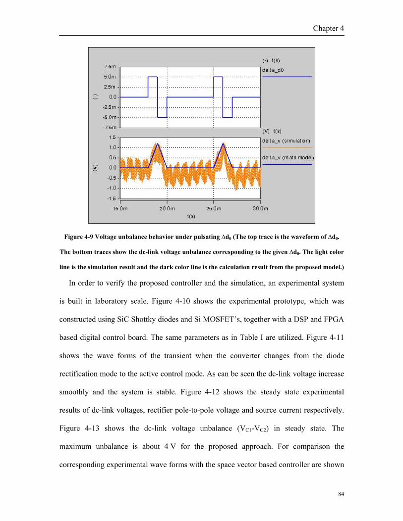
Chapter 4
84
Figure 4-9 Voltage unbalance behavior under pulsating ∆d0 (The top trace is the waveform of ∆d0.
The bottom traces show the dc-link voltage unbalance corresponding to the given ∆d0. The light color
line is the simulation result and the dark color line is the calculation result from the proposed model.)
In order to verify the proposed controller and the simulation, an experimental system
is built in laboratory scale. Figure 4-10 shows the experimental prototype, which was
constructed using SiC Shottky diodes and Si MOSFET’s, together with a DSP and FPGA
based digital control board. The same parameters as in Table I are utilized. Figure 4-11
shows the wave forms of the transient when the converter changes from the diode
rectification mode to the active control mode. As can be seen the dc-link voltage increase
smoothly and the system is stable. Figure 4-12 shows the steady state experimental
results of dc-link voltages, rectifier pole-to-pole voltage and source current respectively.
Figure 4-13 shows the dc-link voltage unbalance (VC1-VC2) in steady state. The
maximum unbalance is about 4 V for the proposed approach. For comparison the
corresponding experimental wave forms with the space vector based controller are shown
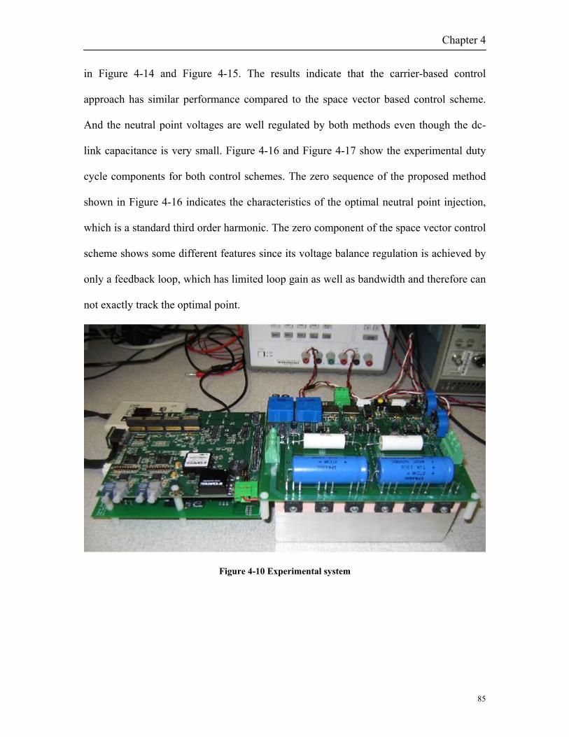
Chapter 4
85
in Figure 4-14 and Figure 4-15. The results indicate that the carrier-based control
approach has similar performance compared to the space vector based control scheme.
And the neutral point voltages are well regulated by both methods even though the dc-
link capacitance is very small. Figure 4-16 and Figure 4-17 show the experimental duty
cycle components for both control schemes. The zero sequence of the proposed method
shown in Figure 4-16 indicates the characteristics of the optimal neutral point injection,
which is a standard third order harmonic. The zero component of the space vector control
scheme shows some different features since its voltage balance regulation is achieved by
only a feedback loop, which has limited loop gain as well as bandwidth and therefore can
not exactly track the optimal point.
Figure 4-10 Experimental system
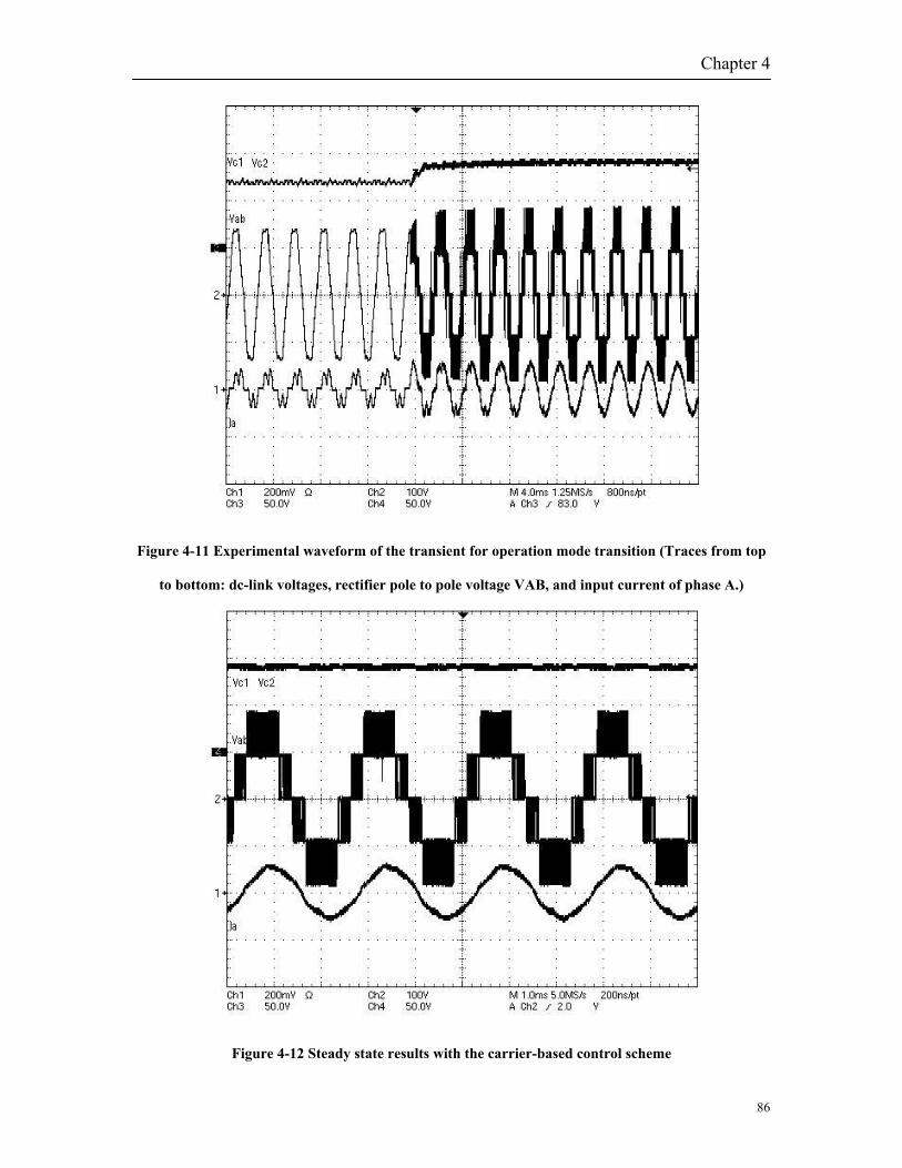
Chapter 4
86
Figure 4-11 Experimental waveform of the transient for operation mode transition (Traces from top
to bottom: dc-link voltages, rectifier pole to pole voltage VAB, and input current of phase A.)
Figure 4-12 Steady state results with the carrier-based control scheme

Chapter 4
87
Figure 4-13 Dc-link voltage unbalance with the carrier-based control scheme
Figure 4-14 Steady state results with the space vector based control approach

Chapter 4
88
Figure 4-15 Dc-link voltage unbalance with the space vector based control approach
1 1.5 2 2.5 3 3.5 4 4.5 5
x 10-3
-1
0
1duty cycle
1 1.5 2 2.5 3 3.5 4 4.5 5
x 10-3
-0.5
0
0.5zero component
t(s)
Figure 4-16 Measured duty cycle components of the proposed carrier-based control scheme (The top
traces are the duty cycles for three phases. The bottom trace is the zero sequence component.)

Chapter 4
89
1 1.5 2 2.5 3 3.5 4 4.5 5
x 10-3
-1
0
1duty cycle
1 1.5 2 2.5 3 3.5 4 4.5 5
x 10-3
-0.5
0
0.5zero component
t(s)
Figure 4-17 Measured duty cycle components of the space vector control scheme (The top traces are
the duty cycles for three phases. The bottom trace is the zero sequence component.)
4.5 Space Vector Analysis
Space vector representation is a powerful tool for the analysis of three-phase converter
since it provides the clear insight for the terminal voltage and current behavior. In this
section space vector analysis is carried out to study the neutral voltage balance
mechanism and the feasible operation region under the balance condition.
A. Neutral Point Voltage Balance Mechanism
According to the symmetry of space vectors, only 60° needs to be considered as
shown in Figure 4-18. 1 and 0 represent the on and off states of the corresponding switch
respectively. And φ is the angle between the vector (0,0,0) and the reference voltage
vector. In sector I, if φ is smaller than 30°, (1,0,0) and (0,1,1) point to the same vector. If
φ is larger than 30°, (1,1,0) and (0,0,1) point to the same vector. Although these

Chapter 4
90
redundant vectors have the same voltage representation in the α-β plane, they lead to
different current injection into the neutral point. For instance, in the first 30° region,
(1,0,0) indicates the midpoint injecting current to be iA while (0,1,1) leads to -iA. In the
second 30° region, (0,0,1) and (1,1,0) indicate the current injection of iC and –iC
respectively. Assuming the line current is in phase with the reference voltage, the
redundant vectors are always charging or discharging the dc link midpoint with the
maximum line current. Therefore the combination of these redundant vectors can be used
to balance the neutral point voltage as an extra control variable in the space vector based
approach [19].
refvv
ϕ
Figure 4-18 Space vector diagram in 60º
For example, if the reference voltage vector lies in sub-sector 2, the corresponding
relative on-times for the vectors are given by [20].
⎪⎪⎩
⎪⎪⎨
⎧
⋅⋅=
−°+⋅⋅=
°+⋅⋅−=+
)sin(3
1)30cos(3
)60sin(32
)0,1,0(
)0,0,0(
)1,1,0()0,0,1(
ϕ
ϕ
ϕ
Md
Md
Mdd
. (4-22)
where M is the modulation index defined as the peak phase voltage over half of the DC
link voltage.

Chapter 4
91
Notice that the first equation of (4-22) shows the redundant vectors (1,0,0) and (0,1,1)
corresponding to sub-sector 2. And there are infinite solutions. In order to achieve zero
neutral point current injection, the relative on-times in (4-22) should be also subject to
0)( )1,1,0()0,0,1()0,1,0( =⋅−+⋅ AB iddid . (4-23)
With (4-22) and (4-23) the relative on-times of the voltage vectors can be achieved.
Due to the characteristics of current force commutation, the phase leg duty cycles can be
given by
⎪⎪⎩
⎪⎪⎨
⎧
⋅−=
⋅−−=
⋅−=
)sgn()1(
)sgn()1(
)sgn()1(
)1,1,0(
)0,1,0()1,1,0(
)0,0,1(
Cc
Bb
Aa
idd
iddd
idd
. (4-24)
where sgn is the signum function. Then the equivalent zero sequence for the space vector
modulation scheme (SVM) can be obtained through
3_0cba
SVMddd
d++
= . (4-25)
Assuming the line currents are in phase with the reference voltage, they are given by
⎪⎩
⎪⎨
⎧
°+⋅=°−⋅=
⋅=
)120cos()120cos(
cos
ϕϕϕ
mC
mB
mA
IiIiIi
. (4-26)
where Im is the amplitude of the line current.
With (4-21)-(4-26) the optimal zero sequence duty cycle for the space vector
modulation scheme in sub-sector 2 can be derived as
°≤≤−⋅= 300)2cos21(
cos2_0 ϕϕϕ
Md SVM . (4-27)

Chapter 4
92
Following the same method, the zero sequence leading to zero neutral current injection
for the other sub-sectors can be derived. The analysis results show that the optimal zero
sequence is only the function of M and φ regardless of the sub-sector location. For
example, When 30°≤ φ ≤60°, the zero component is given by
)6030(cossin3
)cossin3(cos_0 °≤≤°
+
−⋅⋅= ϕ
ϕϕϕϕϕMd SVM . (4-28)
With the same assumption, substituting φ for ω0t in (20) leads to
)2cos21(
cos2'0 ϕ
ϕ−⋅=
Md . (4-29)
(4-28) and (4-29) show that in sub-sector 2 the space vector based control scheme has
the same zero sequence duty cycle as the proposed carrier based control scheme. Actually
this conclusion stands for all the other sub-sectors. This analysis indicates that the
proposed control approach is the same as the space vector approach from the math
standpoint. But the zero sequence in the carrier-based method is generated in a partially
feed-forward way instead of going through the complicated space vector modulator.
B. Operating Region Analysis
In general, the zero sequence injection technique is used in the carrier-based
modulation scheme in order to increase the possible modulation index [42]. However, the
zero sequence component in this work is derived from the neutral voltage balance
standpoint instead. Therefore its impact on the operating region (feasible modulation
index) needs to be investigated.
The analysis can be carried out based on the vector synthesis equations. For example,
if the target reference voltage locates in sub-sector 2 as shown in Figure 4-15, define the
distribution ratio of the redundant voltage vectors as

Chapter 4
93
)1,1,0()0,0,1(
)0,0,1(
ddd
r+
= . (4-30)
After substituting (4-26), (4-30) into (4-22), (4-23) and some algebraic manipulation,
the following relationship can be achieved.
)60sin(32sin3
cos)120cos(21
°+−⋅
°−=−
ϕϕ
ϕϕ
MMr . (4-31)
Since (4-23) is included in the derivation, (4-31) guarantee zero current injection to
the dc link midpoint. For a feasible solution, the distribution ratio r should be within the
range between 0 and 1, which leads to
1211 ≤−≤− r . (4-31)
With (4-31) and (4-32) the upper boundary for the modulation index can be obtained
as
)602sin(3cos2
°+≤
ϕϕM . (4-32)
In sub-sector 2, 0≤ φ ≤30°, therefore the minimum upper boundary in (4-32) can be
achieved when φ = 30°, as
32
≤M . (4-33)
(4-33) indicates that the full modulation index can be achieved in sub-sector 2 when
considering zero current injection to the dc link midpoint. The approach is applied to the
other sectors and the results lead to the same conclusion. The full modulation index can
be achieved when using the optimal zero sequence injection.

Chapter 4
94
4.6 Summary
This chapter presented a new average model for the non-regenerative three-level boost
(Vienna-type) rectifier using the concept of zero neutral point current injection. The
optimal zero sequence duty cycle is found to guarantee the dc-link voltage balance, based
on which an equilibrium operating point can be found and the behavior of the neutral
point voltage deviation can be modeled as a simple first order system. The proposed
model features extended frequency range (up to half of the switching frequency) using
the conventional d-q representation and therefore can be applied for the high performance
controller design. Based on the proposed model a carrier-based control approach is
developed. The zero sequence duty cycle, which consists of two components, is used to
control the neutral point voltage balance. The feed forward component ensures zero
current injection to the neutral point with simple calculation and the feedback component
compensates the non-ideal factors in the real system. The space vector analysis shows
that the proposed control approach is the same as the space vector based control approach
from the math standpoint while it achieves the zero sequence duty cycle in a partially
feed forward way. Therefore the proposed control method can significantly reduce the
calculation effort. The analysis also proves that that with the optimal zero sequence duty
cycle the full modulation index can be still achieved. The proposed model and control
scheme are verified by both simulation and experimental results.

Chapter 5
95
Chapter 5 Failure Mode Analysis and Protection
This chapter investigates the failure modes and protection approaches related to the
structure of the circuit and the characteristics of SiC devices. A fault type unique to three-
level converter including Vienna-type rectifiers, the dc-link voltage-doubling fault, is first
introduced. Then two types of protection methods are proposed, discussed and analyzed:
the voltage-clamping and the current-breaking protection schemes. The impact of ac
inductors on the voltage-doubling phenomenon is studied carefully, and a guideline for
the protection scheme selection is provided. This failure mode and the current breaking
protection scheme are fully analyzed and verified by simulation and experimental results.
This chapter also develops a special protection approach for the shoot-through failure that
is suitable for the voltage source converter system built with SiC JFETs. Design
considerations are presented, and experiments demonstrate the feasibility of the proposed
failure protection.
5.1 Introduction
Failure mode detection and protection is an important aspect for any converter system,
especially high-power converters in critical applications where high reliability is required.
Therefore, a detailed failure mode analysis and corresponding protection scheme
development should be considered in the converter design stage. There are many factors
that can lead to faults, such as incorrect operation, loose mechanical connections, and
component malfunction. Among these, semiconductor device failure, including short or
open of both switches and diodes, is one of the most common faults in a converter. For
multi-level converters, the probability of device fault and the modes of failure increase

Chapter 5
96
due to the complicated topology and the large number of devices. Although there has
been a great effort to analyze the Vienna-type rectifier [52] [84] [85], most of this work
has focused on modulation and control schemes development, with only a few limited
studies on failure modes and faults of three-level neutral-point-clamped (NPC) converters,
which includes the Vienna-type of converters [89]. These mainly focus on short-circuit
and over-current protections [90] [91] [92], or on fault-tolerant control and operation
[93]-[100]. The failure mode related to the neutral switching cell and the impacts of the
system parameters remain unclear.
Addressing the above, this chapter first focuses on analysis and protection scheme
development for the neutral ac switch short-circuit fault in Vienna-type converters.
Specifically, it deals with the voltage doubling behavior under this fault condition—
unique to three-level NPC structures, and analyzes two different types of protection
schemes, namely voltage clamping and current breaking. For the voltage-clamping
approach, a simplified design method for the conventional resistor clamping is first
developed. Then a protection circuit with varistor clamping is proposed and discussed,
which shows a better performance than the resistor clamping. The impact of the input
inductance and the dc-link clamping voltage is also investigated, showing that the peak
fault current and the power dissipation in the dc-link are proportional to the inverse of the
ac inductance when using the voltage-clamping approach. An experimental setup has
been constructed and used for verification purposes, demonstrating the validity and good
results obtained by the proposed protection schemes. Although the discussions in this
work are based on Vienna-type rectifiers, the results and conclusion apply to other three-
level NPC converters as well.

Chapter 5
97
Shoot-through failure is another concern for the converter system. The dc-link positive
bus and negative bus are directly shorted during a shoot-through failure, and the shoot-
through current can reach a level several times higher than the peak current limit of the
semiconductor devices in just microseconds. For this reason, the key challenges for
designing an effective protection approach are to detect the fault current and to block the
short circuit loop within a very short time, which should be in the range of 3 to 10 μs
[102]. The de-saturation characteristic of IGBT is usually utilized to detect an over
current fault for a converter system built with IGBTs. The detection can be integrated
into the gate driver and the protection function can be achieved with an auxiliary logic
circuit [103]. This technology has been widely used in commercial gate drivers. However,
the situation differs for converter systems built with SiC JFETs, because of the limited
knowledge of the characteristics of these new devices. In addition, the de-saturation
approach cannot protect the SiC JFETs from shoot-through failure when losing the gate
drive power since they are normally-on devices. Therefore it is a necessity to design a
protection circuit that can fill the need created by the SiC JFET devices.
This chapter proposes a novel shoot-through protection scheme, which is especially
suitable for a converter system built with SiC JFETs. A bi-directional switch cell is
embedded in the dc-link capacitor tank, with which the functions of shoot-through
protection and dc-link capacitors pre-charge can be achieved. Section II explains the
operation mechanism of the protection circuit. Section III describes some considerations
for the parameter selection and presents the gate drive circuit. An experimental system is
built and to verify the feasibility of the proposed protection approach.

Chapter 5
98
5.2 Neutral Switch Shorted Failure of Vienna-Type Rectifier
5.2.1 Fault Mechanism Analysis
L
i+
i-
ineu
io+
io-
O
A
NL B
vas
vbs
Lvcs C
C1
C2
+
-vC1
+
-vC2
iAiBiC
Qa
Qb
QcR
Figure 5-1 Circuit diagram of the non-regenerative three-level boost rectifier
As shown in Figure 5-1, the phase leg terminals in the Vienna-type rectifier are
connected to the neutral point of the dc-link through ac switches. Any short-circuit failure
of the switching device in these switches leads to a short circuit between the
corresponding phase leg and the neutral point, resulting in an over-voltage failure in the
dc-link. For example, if Qa is shorted, point A is clamped to mid-point N. If all other
healthy switches are assumed to open once the fault is detected, the equivalent circuit
under the fault is like the one shown in Figure 5-2. In this figure, when VA is positive and
VB and VC are negative, capacitor C2 charges to the peak voltage of VAB and VAC, as the
remaining circuit acts as a diode bridge. The charging currents are indicated by the
arrows shown in Figure 5-2. On the following half line-cycle, capacitor C1 is accordingly
charged to the peak voltage of VBA and VCA.

Chapter 5
99
Figure 5-2 Circuit structure when Qa is shorted
Figure 5-3 Simulation results during the Qa short: the top traces are capacitor voltages, the bottom
traces are input currents
Figure 5-3 shows the simulation results for the case when Qa is shorted. The
simulation parameters used were: input inductance of 150 μH, input phase voltage of
230 V rms and 400 Hz, dc-link load of 42 Ω, and dc-link of 650 V (Vc1 and Vc2 equal 325
V). The load resistor is assumed to be disconnected once the fault is detected. At time t =
20 ms, S1 is shorted and the other two switches are open when the over-voltage condition

Chapter 5
100
is detected. Assuming the source voltages remain unchanged, voltage Vc1 rises to 620 V
and Vc2 rises to 750 V. The peak half DC voltage is higher than the peak line-to-line
voltage due to the energy stored in the input inductors. Compared with the normal
operation, where the peak line-to-line voltage is equally shared by C1 and C2, the voltages
across the dc-link capacitors is basically doubled.
Although the previous analysis is based on the Vienna-type rectifier, it can be applied
to any other three-level NPC converter where similar failure modes will be found. In
principle, the dc-link voltage doubling can occur for inner device short circuits in both
source-side and load-side converters, as long as the ac line-to-line terminal voltages are
present during the fault. For instance, in a high-power drive application, the source side
usually is connected to the utility grid through an electromechanical switchgear. These
take several cycles (on the order of tens of ms) to open when a fault occurs: therefore
they will continue feeding the fault in its occurrence. This same behavior is seen when
driving synchronous motors, i.e., the terminal voltage remains during the fault, but not
when driving induction motors where the voltage would drop, quickly minimizing the
fault effect. In this work the focus is on the analysis and protection of the source-side
converter.
5.2.2 Over Voltage Protection
As can be seen in Figure 5-3, the voltage across the dc-link capacitors will greatly
exceed their voltage rating as well as that of the semiconductors when a short-circuit fault
occurs. A protection scheme must then be designed to prevent this over-voltage condition.
Based on the above analysis, there are two general approaches to limit the dc-link over-

Chapter 5
101
voltage: 1) a voltage-clamping circuit; and 2) a current-breaking circuit in the charging
loop. These two schemes are discussed below.
A. Voltage Clamping Approach
Figure 5-4 (a) shows the basic circuits for the clamping approach. In normal operation,
switches S1 and S2 are open and the protection circuit does not affect the system. When
an over-voltage is detected, the switches are closed and the resistors are connected to the
capacitors. In this way the extra energy caused by the fault is dissipated, clamping the dc-
link voltage. The actual voltage reached during the fault and the power dissipation is
highly dependent on the system parameters, such as input voltage, input inductance, and
the clamping resistance. Therefore the protection circuit must be designed according to
these parameters and the worst-case system conditions.
(a) (b)
Figure 5-4 (a) Diagram for the voltage clamping protection circuit, (b)
simplified circuit for peak voltage approximation
In the fault shown in Figure 5-2, C1 is charged by the peak line-to-line voltage in a
half line-cycle with the highlighted current direction, and C2 is charged in the following
half line-cycle with opposite current direction. If the capacitance value is the same for

Chapter 5
102
both capacitors (as is expected per the design), the voltage across each capacitor can be
roughly approximated by the circuit shown in Figure 5-4 (b). The positive half line-cycle
represents the charging period for capacitor C2, while the negative half line-cycle
represent the charging of C1 with opposite voltage polarity. The failure mode behavior of
the converter can then be approximated by a second-order circuit with sinusoidal
excitation. The peak voltage across the capacitor is then given by
RLjLCV
V
pll
pC
ωω 221
12_
_
+−≈ (5-1)
where Vll_p is the peak line-to-line voltage, ω is the line frequency and R is the clamping
resistance. Equation (5-1) can accordingly be used to design R. For example, using the
simulation parameters in the previous section, if the clamping voltage is set to 450 V, the
required clamping resistance is 0.9 Ω.
Figure 5-5 Simulation results for resistor clamping

Chapter 5
103
Figure 5-6 Simulation results for varistor clamping
The simulation result with resistor clamping is shown in Figure 5-5. The peak voltage
across the capacitor is 430 V, which is close to the design value indicating that (5-1) can
be used to design the clamping resistance The peak value of the fault input current is
450 A and the average power dissipation across the resistor is 78 kW. The rating of the
resistor can be determined based on the power dissipation and the fault clear time.
Figure 5-5 shows simulation results of the proposed protection scheme where very
high fault currents are observed on the input side. (With magnetic saturation, these fault
currents could be even higher). There are high fault currents on the input side because the
dc-link capacitors are always being discharged by the clamping resistors; therefore the
average capacitor voltage is relatively low at the expense of a high fault current. In order
to reduce the fault current and the power dissipation in the protection circuit, a voltage
clamping circuit using a varistor is proposed instead.

Chapter 5
104
The varistor is a variable resistor. When the voltage across the varistor is lower than a
threshold level, the varistor shows a very high resistance; when the voltage increases
above the threshold, the resistance diminishes sharply. This characteristic is usually
expressed in the following way [101]:
αqVI = (5-2)
where q and α are the coefficients dependent on the varistor material. At low voltage,
even when switches S1 or S2 in Figure 5-4 (a) are closed, the energy stored in the
capacitor will not be discharged by the varistor. At high voltages, with dramatically lower
resistance, the capacitor over-voltage will be clamped to the varistor threshold voltage.
Figure 5-6 shows the simulation results for the varistor clamping approach using varistor
VE24P01750K from AVX (α=30, q=1.0737×10-79). As can be observed from this figure,
the peak voltage is clamped to 450 V and the fault current is reduced to 200 A; the power
dissipation is 29.4 kW.
B. Impact of Input Inductance and Clamping Voltage
The input inductance of the converter has a significant impact on the failure mode
evolution, particularly on the input current and the dc-link power dissipation during a
fault. This is analyzed as follows, where, in order to simplify the study, the voltages
across the dc-link capacitors are assumed to be fixed at their maximum feasible value
during the fault, which is determined by both the capacitor and semiconductor device
ratings. This assumption corresponds to the best scenario from the fault current
standpoint, since the dc link voltage remains constant at a high level helping suppress the
fault current.

Chapter 5
105
(a) (b)
(c) (d)
Figure 5-7 (a) Input current waveform in positive half cycle, (b) mode
1, (c) mode 2, and (d) mode 3
According to the condition states of the diodes, there are three distinct periods or
operating modes during an ac switch fault. Figure 5-7 (a) shows the typical waveforms
for currents iA, iB, and iC observed during the three periods t0–t1, t1–t2, and t2–t3 within a
half line-cycle. Figure 5-7 (b)–(d) show the respective equivalent circuits for the different
modes. In this analysis, the ac source voltage in Figure 5-1 is assumed to remain
sinusoidal during the fault, which is given by
⎪⎪⎪
⎩
⎪⎪⎪
⎨
⎧
−=
−=
=
)34cos(
)32cos(
)cos(
πω
πω
ω
tVV
tVV
tVV
mcs
mbs
mas
(5-3)

Chapter 5
106
where Vm is the amplitude of the phase voltage. For convenience, the clamping voltage
Vcap is defined as in (5-4), where k is a constant ratio.
mcap VkV ⋅= (5-4)
Mode 1 (t0 ≤ t < t1): Capacitor C2 is charged by Vas and Vbs through the neutral short-
circuit path and Dbn (Figure 5-2). The voltages across the inductors of Phase A and Phase
B are respectively given by
⎪⎩
⎪⎨⎧
−=
−+=
LaLb
mLa
VV
ktV
V ])6
cos(3[2
πω (5-5)
Mode 2 (t1 ≤ t < t2): All the three phases of the input source are feeding the capacitor C2.
Both Dbn and Dcn are conducting current. The voltages across the inductors are given by
⎪⎪⎪
⎩
⎪⎪⎪
⎨
⎧
+−=
+−=
−=
]31)
34[cos(
]31)
32[cos(
]32)[cos(
ktVV
ktVV
ktVV
mLc
mLb
mLa
πω
πω
ω
(5-6)
Mode 3 (t2 ≤ t < t3): Similarly to Mode 1, the capacitor is charged by Phase A and Phase
C through Dcn. The inductor voltages can be obtained as
⎪⎩
⎪⎨⎧
−=
−−=
LaLc
mLa
VV
ktV
V ])6
cos(3[2
πω (5-7)
The inductor volt-second balance condition can be applied to obtain,
⎪⎪⎩
⎪⎪⎨
⎧
==Δ
==Δ
∫
∫01
01
3
1
2
0
t
tLcc
t
tLbb
dtVL
i
dtVL
i (5-8)

Chapter 5
107
and considering the natural commutation characteristics of the diodes, the transition times
for the operating modes can be found as (5-9), where T is the fundamental line cycle.
⎪⎪⎪
⎩
⎪⎪⎪
⎨
⎧
=−
−=
−−=
discont.) is I(when 2
discont.) is I(when /]6
)3
[arccos(
/]32)
31[arccos(
a03
a0
1
Ttt
kt
kt
ωπ
ωπ
(5-9)
Equations (5-8) and (5-9) indicate that the transition times are only a function of k for a
given fundamental line frequency.
In equations (5-3) to (5-9), the correlation between the peak fault current and the input
inductance is given by (5-10). The expression for the average power dissipation in the dc
link is given by (5-11), with f(k) and g(k) representing functions of k. As seen above, both
ipeak and Pdiss are inversely proportional to inductance L.
)(kfL
Vi m
peak = (5-10)
)(2
kgL
VP m
diss = (5-11)
Figure 5-8 and Figure 5-9 show the peak fault current and dc-link power dissipation
under different input inductances and clamping voltages. A 400 Hz fundamental
frequency is assumed in the analysis. As can be seen from these figures, higher input
inductance and higher k always lead to lower peak fault currents and power dissipation.
From this standpoint, the clamping voltage selection of the protection circuit should be as
high as possible while meeting the component ratings. Figure 5-8 and Figure 5-9 also
indicate that the fault current and power dissipation increase dramatically when the input
inductance is low. In the real system the magnetic core of the inductors would normally

Chapter 5
108
saturate during the fault worsening the results of the failure. In consequence, the voltage-
clamping protection approach is deemed inappropriate for a converter system with low
input inductance.
0
12
3x 10⁻³
11.2
1.41.6
1.80
200
400
600
800
kL (H)
ipea
k (A
)
Figure 5-8 Impact of L and k on the peak fault current
0
12
3x 10⁻³
11.2
1.41.6
1.80
2
4
6
8
x 104
kL (H)
Pis
s (W
)
Figure 5-9 Impact of L and k on the dc-link power dissipation

Chapter 5
109
C. Current Breaking Approach
The second approach to over-voltage protection is to add a current-breaking circuit in
the charging loop, as shown in Figure 5-10. The additional current breaker Sw can be
realized by semiconductor devices, such as a pair of IGBTs or MOSFETs. In normal
operation Sw is always closed, but once the over-voltage across the capacitor is detected
it opens immediately, interrupting the neutral charging loop path. Under this condition,
the converter turns into a two-level diode bridge rectifier. Figure 5-11 shows simulation
waveforms obtained with the current-breaking approach. These results show that the
capacitors are over-charged and that the fault current is low compared to the voltage-
clamping approach. Additionally, no energy absorption units are required in the dc-link
during the fault. However, switch Sw is always connected in series with the neutral
switches increasing the converter semiconductor losses.
L
O
A
NL B
vas
vbs
Lvcs C
C1
C2
+
-vC1
+
-vC2
Sw
Figure 5-10 Circuit diagram for current breaking approach
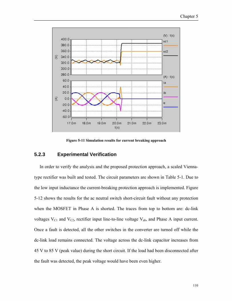
Chapter 5
110
Figure 5-11 Simulation results for current breaking approach
5.2.3 Experimental Verification
In order to verify the analysis and the proposed protection approach, a scaled Vienna-
type rectifier was built and tested. The circuit parameters are shown in Table 5-1. Due to
the low input inductance the current-breaking protection approach is implemented. Figure
5-12 shows the results for the ac neutral switch short-circuit fault without any protection
when the MOSFET in Phase A is shorted. The traces from top to bottom are: dc-link
voltages VC1 and VC2, rectifier input line-to-line voltage Vab, and Phase A input current.
Once a fault is detected, all the other switches in the converter are turned off while the
dc-link load remains connected. The voltage across the dc-link capacitor increases from
45 V to 85 V (peak value) during the short circuit. If the load had been disconnected after
the fault was detected, the peak voltage would have been even higher.

Chapter 5
111
Figure 5-13 shows the experimental waveforms for the same fault under the current-
breaking protection scheme. The protection signal is triggered by the over-current in this
case. The results obtained show that both the peak voltage and the fault current are indeed
reduced to within specified levels, verifying the effectiveness of the proposed protection
scheme for non-regenerative three-level boost rectifiers.
Table 5-1 Parameters Used in Experiment
Source voltage 30 Vrms Source frequency 400 Hz DC link voltage 90 V
Switching frequency 40 kHz Input inductance L 150 µH DC link capacitor C 40 µF/each Load resistance R 50 Ω
Figure 5-12 Experimental waveform neutral switch shorted failure without protection

Chapter 5
112
Figure 5-13 Experimental waveform neutral switch shorted failure with current breaking protection
approach
5.3 Shoot-Through Failure and Protection
5.3.1 Proposed Protection Approach
The protection concept is presented in Figure 5-14. The key idea is to embed a fast
response bi-directional switch into the dc-link capacitor tank. The protection circuit is
highlighted by the dashed frame. The protection circuit consists of an IGBT (S2), an anti-
parallel diode (D1), a relay (S1) and a charging resistor (Rcd). The protection circuit is
embedded into the neutral point between the two dc capacitors so that it will not impact
the main power transmission through the positive and negative dc bus.
Usually the dc source side will have higher high frequency impedance compared to the
dc capacitor tank due to the line inductance. For example, if the dc voltage is achieved

Chapter 5
113
through bridge rectification as shown in Figure 5-14, the input inductor L will limit the
current when the fault occurs. Therefore when the shoot-through occurs, most of the
short-circuit current will have to go through the dc-link capacitor tank at the beginning
instant. Then the embedded protection circuit can be used to detect and clear the fault.
Figure 5-14 Proposed protection circuit
Figure 5-15 illustrates the circuit operation for different mode. For simplicity, switch S
represents the combination of the relay and the IGBT. When the system starts up, the
switch is open, and the dc-link capacitors are charged through the resistor Rcd. This stage
is called dc-link pre-charge, as shown in Figure 5-15 (a). Once the dc link voltage is
charged to the given value, the relay and the IGBT are controlled to be closed, as shown
in Figure 5-15 (b). The main power will go through the positive and negative dc rails and
the ripple energy will go through the capacitor-switch path. Both the IGBT and diode will
conduct ripple current. Figure 5-15 (c) shows the situation for the fault case. Rdson
represents the on resistance of the devices in the shorted phase leg, and Lparasitic represents
the short-circuit loop parasitic inductance. If a short circuit occurs in the inverter stage,
the short-circuit current goes through the dc-link capacitors, the relay and the IGBT. The

Chapter 5
114
IGBT exhibits a de-saturation feature above a certain collector current level, depending
on the gate drive voltage. The collector-emitter voltage increases rapidly. Then the fault
can be detected and cleared by the IGBT and its corresponding gate driver, regardless of
what devices are implanted in the inverter bridge. Figure 5-15 (d) shows the circuit
diagram after a fault is detected. The IGBT is open and therefore the short circuit current
is limited by the charging resistor. In the meantime, a fault signal will be sent out to lock
the active switches in the converter.
Rcd
… to inverter
… to inverter
Vdc
Idc
Vg
high
S
Co
Co
(a) Start up (dc-link pre-charge) (b) Normal operation
(c) Shoot-through (before protection) (d) Shoot-through (after protection)
Figure 5-15 Modes of operation

Chapter 5
115
5.3.2 Gate Driver Circuit Design
In order to implement the protection concept, the gate drive voltage level for the IGBT
has to be determined appropriately, and the corresponding gate driver circuit needs to be
designed. Saturation current level and the conduction loss are the key factors for the gate
drive voltage level selection. Usually lower gate drive voltage will lead to lower de-
saturation current but it also leads to higher conduction loss. In terms of protection, the
de-saturation current level can not be too high, or the devices in the shorted phase leg
may be destroyed before the fault is cleared. On the other hand, under normal operation,
the voltage drop across the collector and emitter of the IGBT should be as low as possible
in order to minimize the conduction loss raised by the protection circuit itself. In most
cases these two requirements have contradictory effects on the gate drive voltage level, so
a tradeoff needs to be made in the practical design based on the system conditions and
requirements.
The gate driver for the protection circuit has three functions: driving the IGBT, over-
current detection and protection, and driving the coil of the relay. The first two functions
are combined together in many commercial gate driver chips. However, the driving
voltage for the relay coil might be different from the required IGBT gate drive voltage.
On the other hand, it is desirable for the gate drive voltage of the IGBT to be adjustable,
which means we can select the current protection level based on the system parameters.
In order to achieve all these functions with only one power supply, a gate driver circuit
is proposed, as shown in Figure 5-16. The commercial gate driver IR21271 is utilized for
the IGBT driving and protection, which is highlighted with the dashed frame. Other
commercial gate drivers with the same function may be applied. Resistor R1 and R2 form

Chapter 5
116
a voltage divider from which desired gate driving voltage can be achieved by changing
the resistance ratio. The relationship between the gate-to-source voltage and the
resistance is given by (5-12). Vg is the output voltage of the gate driver chip, which is
determined by the supply voltage. A 12 V isolated power supply is utilized in this work.
21
2
RRR
VV gge +⋅= (5-12)
Since the IGBT is not switching during the normal operation, the resistance can be large
and the gate driver loss can be very small. In order to increase the turn-off speed in the
fault transient, Schottky diode D2 is connected parallel to R1. During the turn-off period,
D2 will bypass R1, and the gate-to-source capacitor discharges only through the gate
resistor Rg. D3 is a Zener diode, which can help to constrain the voltage spike that occurs
during the fault transient. D4 is the free-wheeling diode for the relay winding. Under
normal operation, both logic signals gneu and error are high. Once a shoot-through is
detected, the gate driver output will be locked and the error logic signal will appear low,
which can be used to block all the other active switches and inform the control system.
Figure 5-16 Gate driver circuit for protection

Chapter 5
117
Figure 5-17 Experimental setup for shoot-through protection
5.3.3 Experiment Results
An experimental system was built to verify the protection concept and design. Figure
5-17 shows the experimental setup. The dc link capacitors are 40 µF each. The IGBT is
IRG4BC20SD from International Rectifier. The gate driving voltage is selected to be
9.5 V, which leads to the de-saturation current level of 30 A. The driving voltage for the
relay coil is 12 V. A MOSFET and a 0.1 μF decoupling capacitor are connected across
the dc bus to emulate a shoot-through failure.
Figure 5-18 shows the experimental results for the dc link voltage of 300V. At instant
t1, the MOSFET is closed. It forms a short circuit with dc-link capacitor. The MOSFET
drain current Id starts to increase dramatically, and the drain-to-source voltage Vds starts
to drop. At the same time, the collector-emitter voltage of the IGBT starts to increase.

Chapter 5
118
At instant t2, the fault is detected by the gate driver chip. After about 240 ns, which is
a built-in delay in the gate drive chip, the IGBT starts to turn off at t3. At instant t4, the
MOSFET starts to turn off. The response delay of the MOSFET (t4-t2) is about 900 ns.
This is mainly due to the propagation time of the gate driver chip and the peripheral
optical couplers. As can be seen from Figure 5-18, the fault is clear in less than 1.2 µs.
The semiconductor devices are protected from being destroyed by the over-current. Some
oscillations are also seen in the MOSFET drain current during the transient. These are
due to the resonance between the decoupling capacitor and the stray inductance in the
short circuit loop.
Figure 5-18 Experimental results: Traces from top to bottom: gate to source voltage of IGBT (Vge),
drain to source voltage of MOSFET (Vds), drain current of MOSFET (Id) and collector to emitter
voltage of IGBT (Vce)

Chapter 5
119
5.4 Summary
In this chapter, an over-voltage failure mode of non-regenerative three-level boost
rectifiers is identified, in which the dc-link voltage is seen to double when any of the ac
neutral switches of the converter failed in short-circuit mode. Two protection approaches,
voltage-clamping and current-breaking, have been thoroughly analyzed.
In voltage-clamping protection, both a resistor-based and a varistor-based clamping
protection circuits were proposed, but the varistor-based circuit presented much better
performance than the resistor-based circuit. The impact of the ac inductance and the
clamping voltage chosen was studied carefully in this scheme. It was found that a higher
clamping voltage always leads to a lower fault current and less power dissipation,
indicating that the highest possible clamping voltage should be chosen within the safety
margins of the converter capacitor and semiconductor devices. However, it was also
found that the peak fault current and the power dissipation in the dc-link during vary
inversely to the input inductance of the converter, which rules out this protection scheme
for high power density applications with reduced input inductance. The current-breaking
approach on the other hand, showed that it can lead to lower fault currents without any
energy absorption components, at the expense of increased losses of the converter system
during normal operation.
Consequently, the final choice of protection scheme needs to consider the converter
operating conditions and specifications. All the above was verified through
comprehensive analysis, simulations, and tests conducted with an experimental
laboratory prototype. Finally, although the discussions in this work are based on Vienna-

Chapter 5
120
type rectifiers, the results and conclusions apply as well to other three-level NPC
converters.
A unique protection scheme for the shoot-through failure mode is also proposed in this
chapter. A bidirectional switch, which is formed by an IGBT and a relay, is embedded
into the dc capacitor tank to detect and clear the fault occurs in the converter bridge. The
proposed protection scheme did not rely on the characteristics of the semiconductor
devices in the converter. Therefore it can be used to protect against shoot-through failure
in the converter system built with SiC JFETs. The circuit design for the gate driver is also
presented. With the proposed circuit, different driving functions can be achieved by using
only one isolated power supply, which help to minimize the size and the cost of the
protection circuit. The experiments carried out verify the feasibility of the proposed
approach. The shoot-through fault is clear in less than 1.2 µs, and the device in the bridge
is protected from being destroyed.

Chapter 6
121
Chapter 6 Hardware Development and Experiments
This chapter presents the hardware development for a 10 kW three-phase ac-ac
converter with the metric of high weight density. SiC JFETs and SiC Schottky diodes are
selected for the power stage in order to achieve high power and high switching
frequency. Based on the topology analysis in Chapter 3, a Vienna-type rectifier plus a
voltage source inverter is chosen for the hardware system. All the concept and
technologies developed and described in previous chapters, including filter design,
control approach and protection schemes, are implemented and verified in this hardware
system. The hardware design, construction and test results are described in details. At the
end of this chapter, the weight breakdown of the hardware system is analyzed and
compared to the paper design.
6.1 System Configuration and Interface
Figure 6-1 Hardware system circuit diagram
Figure 6-1 shows the circuit diagram for the hardware system. The input filter block
represents the multi-stage three-phase LC filter. The protection circuit embedded in the
dc-link includes the neutral blocking protection for the voltage doubling failure and the
shoot-through protection for the SiC JFET inverter, which are discussed in the previous

Chapter 6
122
chapter. The hardware system is classified into the following sub-systems according to
the functions and layout considerations:
(1) Phase leg modules, which include all the switching devices and the corresponding
gate drive, decoupling capacitors and heatsink. A compact circuit layout design is
normally required for this part in order to reduce the parasitic inductance and then
avoid high peak voltage stress during the switch transition. On the other hand,
good noise immunity is also desired; especially for the gate drive circuit, to
prevent faulty operation of the gate drive signal.
(2) DC bus board, which provides the planar dc bus structure and the connection
interface for the phase modules and protection circuits. The voltage and current
sensors and the corresponding processing circuits are also included on this board.
(3) Input filter, which combines the functions of boost inductor and EMI suppression.
(4) Digital controller, which consists of analog to digital conversion, DSP and FPGA
for control implementation. The control system also includes the auxiliary power
supplies for the control circuits.
Figure 6-2 shows the interface of the system. Converter power stage represents the
combination of the phase leg modules, dc bus board and the input filter. The hardware
system terminals include a three-phase main power input, a 28 V control power input, a
three-phase variable frequency output, and external control buttons. The interconnections
between the controller and the converter power stage include the analog sensor signals
(10 channels for the full system), the error signal generated by the shoot-through
detection, the 24 V power supply for the gate driver and the gate drive signals (9
channels, 3 for the rectifier and 6 for the inverter).

Chapter 6
123
Figure 6-2 Hardware system interface
6.2 Hardware Design and Construction
6.2.1 Digital Controller
A previously developed DSP (ADSP-21160) and FPGA (XILINX-XCV400) based
universal controller is chosen for the control function implementation. Two analog-to-
digital converters AD7864 are included in this controller, which provides 8 channels of
analog-to-digital conversion. However, a total of 10 channels analog signals are required
to be processed for the full system. In addition, the calculation capability of the universal
controller cannot support the high speed operation for the full system. Therefore two
universal controllers are utilized at the same time to control the rectifier and inverter
separately. An interface board is built to provide the necessary interconnection functions,
which include the power management for the controller system, the button signal
isolation, sensor signal fault detection, logic protection and signal buffering. The
structure of the controller is shown in Figure 6-3.

Chapter 6
124
UC AD Board UC AD Board
Interface Board (Signal Processing, Logic Protection, Power Management)
Button Functions:Start/Stop, Emergency Stop,
Reset, Speed Control
Isolated by optical coupler
GateSignal 5.1V
Err &Start
AnalogSignal
12VGate
Signal 5.1VErr &Start
AnalogSignal
12V
28V Input
Rectifier Controller Inverter Controller
GateSignal
Sensor Signal
Shoot through Err 24V
To Converter
Figure 6-3 Structure of the controller
6.2.2 DC Bus Board
The dc bus board is the key interface for all the power components, which is
highlighted with the solid frame in Figure 6-4. The dash frames in this figure represent
the connectors for the inverter and rectifier phase leg modules. As can be seen, the dc bus
board includes the over voltage protection, shoot-through protection and all the sensor
circuits. The dc bus board is designed into a ring shape, which makes it suitable to be
integrated with a motor.

Chapter 6
125
Figure 6-4 Diagram of the dc bus board
The circuit diagram for the protection is shown in Figure 6-5. The IGBT for the shoot-
through detection is IRG4BC20SD from International Rectifier, which features a
saturation current of 35 A at 10 V gate drive voltage. With the current level the JFET in
the inverter phase leg should be safe even in a shoot-through condition if the fault only
last for a short while. For the neutral blocking circuit, a CoolMOS power transistor
IPW60R045CP from Infineon is selected since it has very low on resistance (0.045 Ω at
25 ºC).
In this design the dc-link capacitance is very small, therefore a film capacitor is
utilized for energy storage instead of electrolytic capacitors in order to achieve better
reliability and lifetime. The MKP series dc capacitors from EPCOS are selected with the
rated value of 35 µF/450 V. In addition, some 10 nF/1000 V ceramic capacitors are also
connected to the dc bus for decoupling purpose.

Chapter 6
126
S1
S2
35 μF
5kΩ
D1
50nF
35 μF
300kΩ
300kΩ
V+
V-
Vneu
Figure 6-5 Circuit diagram of the dc bus including protection
Figure 6-6 Voltage sensing circuit

Chapter 6
127
Figure 6-7 Physical structure of the dc bus board
The dc bus board includes 10 sensing signals: 2 channels for input current, 2 for
output current, 2 for input voltage, 2 for output voltage and 2 for dc link voltage. Sensor
HX 15-P from LEM is utilized for the input and output current sensing. For the voltage
measurement, non-isolated operational amplifiers are utilized to achieve low profile and
good performance. Figure 6-6 shows the measurement circuit for inverter output voltage
Vab. The physical layout of the dc bus board is shown in Figure 6-7.
6.2.3 Input Filter
Based on the discussion in Chapter 2, the input filter structure and the corresponding
parameters are designed as shown in Figure 6-8. A customized nanocrystalline toroid
core is selected for the common mode choke. In physical design the peak current is 25 A
and the maximum durable flux density is 0.84 T. The design parameters are shown in

Chapter 6
128
Table 6-1. CX is the film capacitor from EPCOS and CY is the ceramic capacitor from
Panasonic. Figure 6-9 shows the physical structure of the input filter.
Table 6-1 Physical Parameters for the CM Choke
Outer Diameter Inner Diameter Height Number of Turns
6.2 cm 4.8 cm 1.1 cm 48 for the first two stages
30 for the last stage
Lcm
CY1=10nF
Ldm Lcm Ldm
Common Mode ChokeLcm=12mH, Ldm=100uH
CX1=1uF
CY2=10nF
CX2=1uF
RC2=1 ohm
Common Mode ChokeLcm=12mH, Ldm=100uH
Lcm
Common Mode ChokeLcm=4mH, Ldm=35uH
Mai
nsR
ectifier
Ldm
Figure 6-8 Circuit diagram of the input filter
Figure 6-9 Physical structure of the input filter

Chapter 6
129
6.2.4 Phase Leg Module and Gate Drive
The combination of the SiC JFET from SiCED and the SiC Schottky diode from Cree
forms the power stage of the converter. Due to the limited JFET die size (2.4 mm by 2.4
mm) the parallel structure is implemented for the phase leg construction to achieve a high
current capability. The number of devices in parallel is determined by the power rating.
Figure 6-10 shows the circuit diagram of the rectifier phase leg. Two JFETs are
connected in parallel for the neural switching cell. 1200 V/20 A SiC diodes are selected
for D1 and D2 while 1200 V/10 A diodes are chosen for D3 and D4. The circuit diagram
for the inverter is shown in Figure 6-11. The switching cell in inverter phase leg consists
of three JFETs and one 1200 V/10 A diode.
Figure 6-10 Rectifier phase leg
Figure 6-11 Inverter phase leg

Chapter 6
130
SiC JFET is a normally-on device and a negative gate to source voltage is required to
turn it off. In addition, the pinch-off voltage as well as the breakdown voltage is device
and temperature dependent [104], and the tolerable voltage window between these two
values is very narrow. In this hardware system a “RCD” gate driver circuit [104] is
implemented to cope with the large variability in the gate characteristics. With this circuit
the JFET gate can operate in avalanche without damage. Other than the special
requirements of the JFET device, a short signal propagation delay-time, a good edge
shape and a good common-mode transient immunity are necessary for the gate driver of a
high switching frequency converter. In order to meet these demands, a digital isolator
ADuM5241 and a high speed high current gate driver IXDN409 are used. ADuM5241
offers the high common-mode transient immunity of 25 kV/µs. This characteristic is
particularly important for the SiC converter due to the fast turn-on and turn-off times.
Figure 6-12 shows the gate driver circuit. As can be seen, the devices in parallel share the
same driver chip. But each of them has their own gate resistor and RCD network, which
can compensate for the gate parameters variation from device to device.
D
S
G
RG
RG
IXYSIXDN409
Vcc
GN
D
OUT
IN
AnalogADuM5241VIB
VDD
VOA
GND
VOB
VISO
VIA
GNDISO
-30 V
-30 V
PWM
Figure 6-12 Gate driver circuit

Chapter 6
131
Figure 6-13 Phase leg modules
Figure 6-13 shows the physical structure of the phase leg modules. The gate driver
board is directly mounted on top of the semiconductor devices. In order to verify the
circuit functions, the phase leg modules are tested as a buck converter with resistor and
inductor load. Figure 6-14 shows the test circuit for the inverter phase leg. The top switch
is operating with a constant duty cycle while the gate of the bottom switch is always
negative biased.
Figure 6-14 Test circuit for the inverter phase leg

Chapter 6
132
Figure 6-15 Waveforms of top switch turn on
Figure 6-15 shows the test results when the dc-link voltage is 80 V. A high voltage
peak is observed in Vgs2 during the turn on transient of the top switch, which indicates a
strong cross coupling between the top and bottom switch. This is due to the Miller
capacitors. When the top switch turns on, the voltage across the bottom switch increases
rapidly. A current will be induced via the Miller capacitor and then injected into the gate
drive circuit. Since the impedance of the gate driver is not zero, a voltage peak will be
generated. This voltage peak could falsely turn on the bottom switch and then lead to a
shoot-through fault. A 1.5 nF capacitor is connected to the gate and source terminal in
order to suppress the voltage peak.
Figure 6-16 and Figure 6-17 show the turn-on and turn-off waveforms at 600 Vdc with
the additional gate-to-source capacitor. The turn-on time and turn-off time are about 60
ns. The voltage peak is less than 3 V, which is much less than the previous case. For the

Chapter 6
133
rectifier phase leg module the cross coupling is not a concern since there is only one
active switching cell in each bridge.
Figure 6-16 Waveforms of top switch turn on with additional 1.5 nF capacitor
Figure 6-17 Waveforms of top switch turn off with additional 1.5 nF capacitor

Chapter 6
134
6.2.5 SiC JFET Characterization
Because the SiC JFET is not fully commercialized, a full datasheet is not available. In
this section the characterization results for on-resistance, switching energy and junction-
to-case thermal impedance are shown since they are essential to the loss calculation and
thermal design for the converter system.
20 40 60 80 100 120 140 160 180 2000.2
0.25
0.3
0.35
0.4
0.45
0.5
Temperature (oC)
RDS
,on (o
hm)
Temperature dependence of the on resistance
MeasurementCurve fitting
Figure 6-18 RDS,on versus temperature
Table 6-2 Switching energy under different conditions (@ 25°C)
Test Condition Switch On (μJ) Switch Off (μJ)
150 Vdc, 5 A 18.9 13.4
300 Vdc, 5A 53.9 31.0
450 Vdc, 5 A 93.3 48.3
600 Vdc, 5 A 143.9 69.2
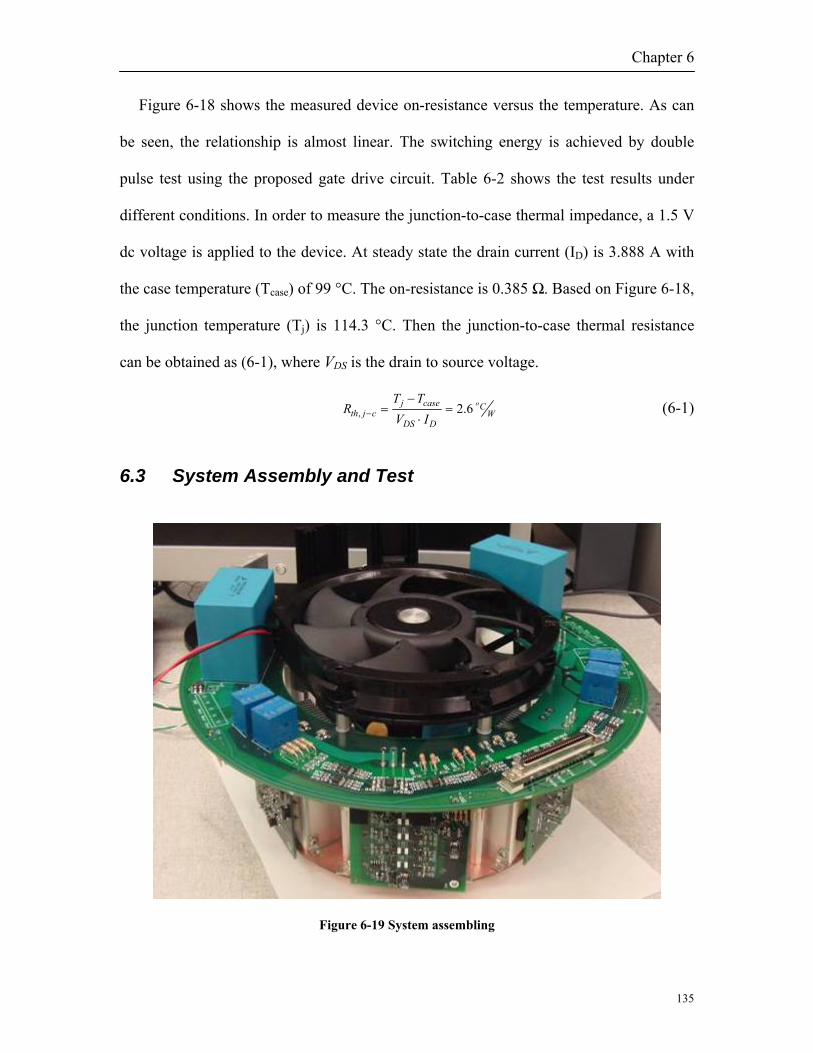
Chapter 6
135
Figure 6-18 shows the measured device on-resistance versus the temperature. As can
be seen, the relationship is almost linear. The switching energy is achieved by double
pulse test using the proposed gate drive circuit. Table 6-2 shows the test results under
different conditions. In order to measure the junction-to-case thermal impedance, a 1.5 V
dc voltage is applied to the device. At steady state the drain current (ID) is 3.888 A with
the case temperature (Tcase) of 99 °C. The on-resistance is 0.385 Ω. Based on Figure 6-18,
the junction temperature (Tj) is 114.3 °C. Then the junction-to-case thermal resistance
can be obtained as (6-1), where VDS is the drain to source voltage.
WC
DDS
casejcjth
o
IVTT
R 6.2, =⋅
−=− (6-1)
6.3 System Assembly and Test
Figure 6-19 System assembling

Chapter 6
136
6.3.1 System Assembly
The six phase-leg modules and the input filter are mounted on a baseplate and then the
dc bus board is connected to the modules via solder, as shown in Figure 6-19. The two
universal controllers and the interface board are assembled in a control box. A 68-pin
mini delta ribbon (MDR) cable is used to connect the control box and the dc bus board.
6.3.2 Controller Structure and Start-up Sequence
As mentioned in the previous chapter, the DSP/FPGA based controller is used for the
control approach implementation. The FPGA is the interface between the peripheral I/O
and the DSP. The AD data and button status are stored in the registers of the FPGA. The
FPGA also realizes the modulation function for the gate signals and generates the
interruption signal which indicates the starting point of a new switching cycle. Once the
DSP detects the interruption signal, it will update all the feedback signals via the
corresponding registers and then carry out the control calculation. When the calculation is
done, the duty cycle will be sent to the FPGA and then translated into the gate drive pulse
signal. Figure 6-20 shows the structure of the controller.
Figure 6-20 Controller structure

Chapter 6
137
Figure 6-21 Start-up sequence
Since the Vienna-type rectifier is non-regenerative, it cannot start from a zero load
condition. Therefore in the experimental system a special start-up sequence is utilized, as
shown in Figure 6-21. The controllers for both rectifier and inverter are running at
iteration mode for sampling and button status detection. Once the start button is pushed,
the rectifier controller compares the current dc-link voltage with the given threshold
value. If the dc-link voltage is higher the dc-relay will be close. At the same time the
inverter will wait until the relay is totally close, which usually take tens of ms. After the
waiting period the inverter runs at open loop control mode to start the motor while the

Chapter 6
138
rectifier runs as a diode bridge. When the inverter runs to a certain power level, the
rectifier starts running at active mode and regulates the dc bus voltage to the reference
value. Then, the inverter starts the close-loop control. Figure 6-22 shows the
experimental waveforms for the startup period. The traces from top to bottom are: dc-link
voltages, rectifier input current and inverter output current.
Figure 6-22 System start-up transient waveforms
6.3.3 Experimental Results
Table 6-3 shows the circuit parameters for the experiments. The steady state
experimental waveforms are shown in Figure 6-23. The traces from top to bottom are: dc-

Chapter 6
139
link voltages, input source current and inverter output current. As can be seen, the dc-link
voltage is well balanced, and both input and output current show good waveform.
Table 6-3 Circuit Parameters for the experiment
Input Voltage 230 Vrms/ 400 Hz Load Resistance 16 Ω
Output Voltage 230 Vrms/400 Hz Load Inductance 1.2 mH
DC-Link Voltage 660 V Power 10 kW
Figure 6-23 Steady state waveforms at full power
Figure 6-24 shows the Fourier analysis result for the input current. For comparison,
the power quality requirement defined in DO-160E is also plotted in the same figure. As
can be seen, the entire harmonics meet the standard except the fourth order, which
exceeds a little bit. The non-ideality of the power source is one of the reasons for the low

Chapter 6
140
frequency current harmonics. In order to improve the harmonic performance, a higher
bandwidth for the current control loop is desired.
0 2000 4000 6000 8000 10000 12000 14000 160000
0.1
0.2
0.3
0.4
0.5
0.6
0.7
0.8
0.9
1
Current spectrumPQ standard
Figure 6-24 Input current spectrum analysis
In order to verify the input filter design, EMI measurement is carried out. The current
probe used for the noise measurement is 91550-1 from ETS-Lindgren. Figure 6-25 shows
the measurement results. The blue line is the noise current spectrum of Phase A. The pink
curve is the total common mode noise current of the three phases and the red dash line
represents the narrow band requirement specified by the standard DO-160E. As can be
seen, the noise spectrum meets the EMI standard up to 800 kHz. This result demonstrates
the EMI filter design concept proposed in Chapter 2 since the L and C parameters are
determined by the relatively low frequency noise. In the frequency range higher than 800
kHz, the standard requirement is not met. The measurement results indicate that in this

Chapter 6
141
frequency range the CM noise is dominant. The grounding condition of the EMI filter
and the relatively high equivalent parallel capacitance (EPC) of the double-layer winding
structure could be the reasons for the high CM noise. It can be improved by reducing the
grounding impedance of the EMI filter.
106 107-10
0
10
20
30
40
50
60
Frequency (Hz)
dBuA
Phase A currentCM currentStandard
Figure 6-25 EMI measurement results
This converter is also successfully tested with a 3 kW axial flux permanent magnet
motor which has 6 pole pairs. The system setup is shown in Figure 6-26. The motor is
connected to the YASKAWA dynamometer via an 8 to 1 gearbox. Table 6-4 shows the
test conditions. Figure 6-27 shows the measurements for the rectifier. The traces from top
to bottom are: dc-link voltages, rectifier line-to-line voltage and input current. Figure 6-
28 shows the measurement results for the inverter. The traces from top to bottom are: dc-

Chapter 6
142
link voltage, inverter line-to-line voltage, inverter output current and rectifier input
current.
Figure 6-26 Motor test setup
Table 6-4 Conditions for the Motor Test
Input Voltage 115 Vrms/ 400 Hz Rotor Speed 5500 rpm
DC-Link Voltage 330 V Torque 5 Nm

Chapter 6
143
Figure 6-27 Measurement results for the rectifier
Figure 6-28 Measurement results for the inverter

Chapter 6
144
6.4 System Efficiency
In order to evaluate the loss calculation and verify the overall thermal design,
efficiency measurement is carried out in scale down power level with the power analyzer
PZ 4000. In this test, the dc-link voltage is 450 V and the input voltage is 160 Vrms. A
1.2 mH three-phase inductor and three 16 Ω resistors are utilized as the three phase load.
The ambient temperature is 25 °C. The load current amplitudes and corresponding
measurement results are shown in Table 6-5.
Table 6-5 Efficiency Measurement
Load Current (A) Input Power (W) Output Power (W) Loss (W) Efficiency
9.43 2343 2238 105 95.3%
11.55 3475 3330 145 95.6%
14.33 5336 5102 234 95.4%
The temperature of the side fin for each heatsink is also monitored during the test. For
the case with 14.33 A load current, the temperature rise at the measurement point are 11
°C for the rectifier and 8 °C for the inverter, which indicates that the rectifier has higher
loss under this condition. Based on the finite element analysis, the thermal resistance for
each heatsink is about 0.45 °C/W. Then the average temperature rise of the heatsink for
this case can be roughly estimated to be 13.5 °C according to the loss measurement.
Considering the non-uniform temperature distribution, the estimation is within a
reasonable range compared to the measurement result. Since we measure the junction-to-
case thermal resistance of the JFET device, the junction temperature can be estimated to

Chapter 6
145
be 56.5 °C for this case assuming a 1 °C/W thermal resistance for the interface between
the heatsink and the device case.
For comparison, the loss calculation results under the same conditions are shown in
Table 6-6. The calculation results show similar trend but lower value. There is about 35%
error for the loss calculation. Several factors may contribute to the discrepancy. First, the
characteristics of JFET are device dependent, and the switching energy highly depends
on the circuit conditions including the parasitic. Therefore the switching loss could be
different from the one achieved by double pulse test. Second, the impact of the switching
ripple is ignored in the calculation. Third, the power in the parallel devices may not be
ideally shared and the on-resistance could be higher than the ideal value. Fourth, the loss
in the interconnection and some other auxiliary components are not included. Fifth, errors
exist for the power and temperature measurement.
Table 6-6 Loss Calculation @ Estimated Junction Temperature of 56.5C
Load Current (A) Rectifier (W) Inverter (W) Filter & Protection (W) Total (W)
9.43 27.3 24 18.1 69.4
11.55 44.5 33.8 30.2 108.5
14.33 79.3 48.2 50.9 178.4
Considering the 35% error, the total loss and junction temperature at full power case
can be estimated. Iteration approach is applied for this calculation. A junction
temperature is first assumed for the loss calculation. And then based on the calculated
loss we recalculate the junction temperature. If this junction temperature is higher or
lower than the previous assumption, we will pick the average value of these two to do the
calculation again. This procedure is iterated until the junction temperature converges to a

Chapter 6
146
constant value. With this approach, the total loss is estimated to be 490 W with a JFET
junction temperature of 90 °C. The system efficiency is 95.1%. It indicates that the high
junction temperature advantage of the SiC JFET is not fully taken. The heatsink and the
fan are oversized.
6.5 Weight Discussion for the Hardware System
In this chapter, all the design concepts and procedures developed in the previous
chapter are investigated and verified by experiments. The converter system can meet the
EMI standard at low frequency range, which proves the integration design concept for the
input filter. The stable operation under different conditions demonstrates the feasibility of
the dc-link capacitor selection as well as the control design. For the heatsink passive,
although there are some errors for the loss calculation, the design approach is still valid in
terms of estimating the size of the heatsink and the junction temperature with some
correction factors. Since high weight density is the key design objective for the converter
system in this work, the weight distribution of the physical system also needs to be
investigated and then compared to the paper design.
Figure 6-29 shows the weight breakdown of the converter system. The total weight of
the system is 2785 g (6.14 lbs.). The power density of the system is 1.63 kW/lbs. As can
be seen, the heatsink, the fan and the input filter dominate the weight of the system.
Before the hardware construction, the paper design is carried out based on the
approaches describe in the previous sections. Table 6-7 presents the comparison between
the real system and the design values.

Chapter 6
147
Weight Distribution of the Hardware System
0200400600800
1000
Hea
tsin
k
Sem
icon
duct
orD
evic
es
DC
cap
Pro
tect
ion
Inpu
t Filt
er
DC
Bus
PC
B
Gat
e D
rive
PC
B Fan
Wei
ght (
g)
Figure 6-29 Weight distribution of the hardware system
Table 6-7 Weight Comparison
Heatsink Devices DC
cap
Prote-
ction Fan
LCLC
Filter
Additional
Inductor
DC
Bus
PCB
Gate
Drive
PCB
Total
Real
Value (g) 768 120 204 100 430 513 183 248 219 2785
Design
Value (g) 318 120 80 80 162 432 1192
The explanations for the weight discrepancy between the design and the real system
are given as following:
• Heatsink and fan are the key contributors to the weight difference. As discussed in
the previous section, these components are over-sized because of an availability
issue for the commercial products.

Chapter 6
148
• Dc-link capacitor: Due to the limitation of the universal controller, the actual
control frequency is 35 kHz for the rectifier although the switching frequency is
70 kHz. We chose 17.5 μF instead of 10 μF for the total dc-link capacitance. On
the other hand, there is also some error when scaling the size of the capacitor
based on energy storage in the design stage.
• LCLC filter: The difference is caused by the winding. In the real system the
weight of the winding is bigger than the designed value due to an estimation error
for the multi-layer winding structure, where the mean length per turn of the outer
layer is longer than the inner layer. But it is ignored in the paper design.
• As explained in the previous chapters, an additional inductor is used to
compensate the impedance of the LISN at low frequency.
• The weight of the printed circuit board and some auxiliary power supplies and
connectors is not considered in the paper design.
6.6 Summary
This chapter presents the hardware development of a 10 kW high power density three-
phase ac-dc-ac converter using SiC JFETs and SiC Schottky diodes. The structure of
parallel devices is implemented for the phase leg to achieve a high power rating and the
corresponding gate driver circuit is proposed and tested. All the technologies and
concepts developed in the previous chapters are applied in this hardware system and a
special start-up sequence in software is developed to cope with the non-regenerative
characteristics of the Vienna-type rectifier. The converter system is tested with full power
and all the key functions are verified. The EMI measurement is also carried out. The low

Chapter 6
149
frequency noise spectrum demonstrates the input filter design. The high frequency noise
does not meet the standard, and there is still room to improve by reducing the ground
impedance of the CM filter. The converter system is also successfully tested with a 3 kW
permanent magnet motor. The efficiency and the heatsink temperature of the system are
measured in a scaled down power level and then compared to the theoretical calculation.
The results indicate that smaller heatsink and fan can be used.
The hardware system achieved 1.63 kW/lbs. The difference between the real system
and the paper design is discussed and analyzed. It shows that a higher density can be
obtained by customizing the heatsink and fan since the ones used in the systems are over-
sized.

Chapter 7
150
Chapter 7 Conclusions and Future Work
This chapter summarized the entire dissertation and discusses some ideas for the
future work.
7.1 Conclusions
This work presents a systematic methodology for the analysis and design of high
power density three-phase ac converter. Four key factors of the converter system,
including topology, passive, control and failure mode, are carefully studied.
First, the parameters selection criteria for both input filter and dc bus energy storage
are developed. The correlation between the switching frequency and the size of the input
filter are investigated when considering EMI standard and power quality requirement. A
non-monotonous relationship was found, accumulating with some favored operating
frequency from the size standpoint. A function integration concept for input filter design
is proposed, which means the input filter, including EMI filter and harmonic filter, can be
designed as an entity based on the output standard requirement and the converter terminal
voltage or current spectrum. The same inductors can be used for EMI suppression and for
boost function. Energy storage and impedance interaction requirements are also set up to
determine the minimum DC link capacitor.
Second, a systematic methodology for a three-phase converter topology evaluation, as
well as the design approach, is proposed. The design objective (size/weight), constraints,
conditions, and variables are clearly defined. All the key size contributors and their
correlations are introduced and analyzed in a systematic way. It provides the design

Chapter 7
151
guideline for both circuit parameter selection and system operation condition
determination. Based on the proposed methodology, 4 candidate topologies are compared.
The results show that the three-phase non-regenerative three-level boost rectifier (NTR)
plus voltage source inverter has a better weight performance under the given conditions.
This approach can be applied to other topologies with different metric.
Third, in order to achieve a high performance control algorithm for a high speed
operation, a wide frequency range average model for the NTR is developed. An
“optimal” zero sequence injection concept is proposed from the voltage balance
standpoint. Based on this concept an equilibrium point for the dc-link neutral voltage
balance can be found and then the average model can be built in the conventional d-q
coordinate. In the proposed model the neutral point behavior is represented by a simple
first order system. The control loop can be easily designed. A carrier-based control
approach is developed by doing the optimal zero sequence injection in a partially feed
forward way. The proposed control approach features great simplicity and good neutral
regulation. Both simulations and experiments verified the validity of the model and the
controller.
Fourth, an over voltage failure mode is identified for the NTR. It is a short failure
associated with the switches and diodes of the neutral legs. The voltage across the
capacitor will double once the failure occurs. Two protection approaches as well as the
input inductance impact are investigated. For the voltage clamping approach, the fault
current and the energy dissipation will increase inversely to the input inductance. It
indicates that a neutral point blocking approach is preferred for the converter system with
low input inductance. The shoot-through failure mode, which is particularly a serious

Chapter 7
152
issue for the converter built with normally-on devices, is also discussed and analyzed. A
unique protection circuit is proposed, which achieves both functions of shoot-through
protection and dc-link pre-charge. The proposed approaches are verified by the
experiments.
In the end, a 10 kW three-phase ac converter is design and built with SiC JFETs and
SiC Schottky diodes. All the design concepts and technologies developed in this work are
implemented into this hardware system. The system is successfully tested to high power
and high switching frequency. The EMI measurement and current harmonics analysis are
carried out and the results verify the validity of the proposed design approaches. The
experimental results also indicate a clear need to further improve the high frequency EMI
performance. A power density of 1.63 kW/lbs is achieved by the experimental system. It
shows a larger weight than the paper design, which is mainly due to the over-sized
cooling system and the printed circuit board. A customized heatsink and fan can help to
further reduce the weight of the converter system.
7.2 Future Work
In order to further improve the power density of the three-phase ac converter, future
work can be carried out in the following directions.
In this work the commercial cooling technologies are chosen in the design, and
there are some errors for the thermal calculation. A delicate model for the thermal
system is desired. Since the heatsink and fan remain the key weight/size
contributors, advanced cooling technologies and package approaches can be
explored to further reduce the size of the cooling system. On the other hand, as

Chapter 7
153
the advantage of SiC devices, the junction temperature of the devices can be
pushed to a higher level, with which the size of cooling system can be further
reduced. This requires a thermal reliability evaluation for the devices and
components. The development of corresponding high temperature auxiliary
circuits and packaging technology is also a necessity.
The EMI filter design approach proposed in this work is based on the low
frequency analysis. The three-phase common choke is designed to achieve a
relatively high leakage inductance for the function integration purpose. That may
exaggerate the coupling issues between the different filter stages and impact the
noise attenuation capability. Further investigation on filter structure and shielding
approach is desired. In addition, the filter behavior at high frequency, including
the grounding impact, and the corresponding approach for improvements needs to
be further analyzed. A full frequency range model for the input filter is desired.
In this dissertation, the average model for the Vienna-type rectifier is built on the
equilibrium point when the dc-link voltage is balanced. How to extend the model
to other operating points can be further explored.
From the system point of view, an advanced modulation scheme or circuit
topology can be studied to reduce the EMI noise. For example, random PWM can
spread out the noise energy in the frequency spectrum, which potentially can
reduce peak noise and then lead to smaller EMI filter. The parallel topology can
be also investigated since it can cancel switching ripple at some specific
frequency range. This will provide new opportunities for the input filter design.

Reference
154
Reference
[1] J. W. Kolar, U. Drofenik, J. Biela, M. L. Heldwein, H. Ertl, T. Friedli and S. D. Round, “ PWM
converter power density barriers,” Power Conversion Conf. (PCC), Nagoya, Apr. 2007, pp. 9-29.
[2] M. Maerz, E. Schimanek and M. Billmann, “Towards an integrated drive for hybrid traction,” Proc.
of Center for Power Electronics Systesm (CPES) Annual Conf., Apr. 2005, pp. 3-7.
[3] M. Pavlovsky, Y. Tsuruta and A. Kawamura, “Pursuing high power-density and high efficiency in
DC-DC converters for automotive application,” IEEE Electronics Specialists Conference (PESC),
Jun. 2008, pp. 4142-4148.
[4] P. K. Jain, “Power electronics for low voltage semiconductor technology: challenges and some
possible solutions,” Proc. of Power Electronics and Motion Control Prof. (IPEMC’04), Aug. 2004,
pp. 20-28.
[5] W. G. Homeyer, E. E. Bowles, S. P. Lupan, P. S. Walia, M. A. Maldonado, “Advanced power
converters for more electric aircraft applications,” Energy Conversion Engineering Conf.
(IECEC’97), Jul. 1997, pp. 591-596.
[6] F. Barruel, JL. Schanen and N. Retiere, “Volumetric optimization of passive filter for power
electronics input stage in the more electrical aircraft,” IEEE Electronics Specialists Conference
(PESC), Jun. 2004, pp. 433-481.
[7] Y. Hayashi, K. Takao, T. Shimizu and H. Ohashi, “High power density design methodology,”
Power Conversion Conf. (PCC), Nagoya, Apr. 2007, pp. 569-574.
[8] L. Lorenz and H. Mitlehner, “Key power semiconductor device concepts for the next decade,” Proc.
of Industry Application Conference, Oct. 2002, pp. 564-569.
[9] P. Friedrichs, “Recent progress in SiC device technology and applications,” CPES Seminar, May.
2006.
[10] I. Omura, M. Tsukuda, W. Saito and T. Domon, “High power density converter using SiC-SBD,”
Power Conversion Conf. (PCC), Nagoya, Apr. 2007, pp. 575-580.
[11] R. M. Cuzner and J. C. VanderMeer, “Impacts to the power density of ship electric drives,” IEEE
Power Electronics Society Newsletter, vol. 16, no. 3, pp.10-12, 2004.

Reference
155
[12] Y. Hayashi, K. Takao, K. Adachi and H. Ohashi, “Design consideration for high output power
density (OPD) converter based on power-loss limit analysis method,” European Conference on
Power Electronics and Applications, Sep. 2005.
[13] G. Gong, M. L. Heldwein, U. Drofenik, J. Minibock, K. Mino, and J. W. Kolar, “Comparative
evaluation of three-phase high-power-factor AC-DC converter concepts for application in future
more electric aircraft,” IEEE Trans. Industrial Electronics, vol. 52, no. 3, pp. 727–737, Jun. 2005.
[14] C. Klumper, F. Blaabjerg, P. Thoegersen, “Alternate ASDs: Evaluation of the converter topologies
suited for integrated motor drives,” Industry Applications Magazine, vol. 12, no. 2, pp. 71-83, Apr.
2006.
[15] Y. Suh, J. K. Steinke, P. K. Stermer, “Efficiency comparison of voltage-source and current-source
drive systems for medium-voltage applications,” IEEE Trans. Industrial Electronics, vol. 54, no. 5,
pp. 2521-2531, Oct. 2007.
[16] R. Teichmann, M. Malinowski, and S. Bernet, “Evaluation of three-level rectifiers for low-voltage
utility applications,” IEEE Trans. Industrial Electronics, vol. 52, no. 2, pp. 471-481, Apr. 2005.
[17] T. G. Habetler, D. M. Divan, “Rectifier/inverter reactive component minimization,” IEEE
Transactions on Industry Application, Volume 25, Issue 2, pp. 307-316, Mar., 1989.
[18] N. J. Wheeler, H. Zhang, D. A. Grant, “Minimization of reactive component values in back-to-back
converters,” Proc. Power Electronics and Variable-Speed Drives, pp. 240-245, 1994.
[19] B. Shi, G. Venkataramanan, and N. Sharma, “Design considerations for reactive elements and
control parameters for three phase boost rectifiers,” Proc. Int. Elect. Machines Drives Conf., San
Antonio, TX, 2005, pp. 1757–1764.
[20] M. Liserre, F. Blaabjerg, S. Hansen, “Design and control of an LCL-filter-basaed three-phase active
rectifier,” IEEE Trans. Ind. App., vol. 41, no. 5, pp. 1281-1291, 2005.
[21] A. Nagel and R. W. De Doncker, “Systematic design of EMI-filters for power converters,” Proc. of
Industry Application Conference, Oct. 2000, pp. 2523-2525.
[22] T. Nussbaumer, M. L. Heldwein and J. W. Kolar, “Differential mode input filter design for a three-
phase buck-type PWM rectifier based on modeling of the EMC test receiver,” IEEE Trans.
Industrial Electronics, vol. 53, no. 5, Oct. 2006, pp. 1649-1661.

Reference
156
[23] P. M. Barbosa, “Three-phase power factor correction circuits for low-cost distributed power
systems,” Ph.D. Dissertation, Virginia Tech, Jul., 2002.
[24] Gu, B.G.; Nam, K, “Theoretical minimum DC-Link capacitance in PWM converter-inverter
systems”, IEE Proceedings of Electric Power Applications, Volume 152, Issue 1, pp. 81-88, 2005.
[25] B. Ray, H. Kosai, J. D. Scofield and B. Jordan, “200 ºC operation of a dc-dc converter with SiC
power devices,” Proc. of APEC 2007, pp. 998-1002.
[26] D. Aggeler, J. Biela and J. W. Kolar, “A compact, high voltage 25 kW, 50 kHz dc-dc converter
based on SiC JFETs,” Proc. of APEC 2008, pp. 801-807.
[27] S. K. Mazumder, K. Acharya and C. M. Tan, “Design of an all-SiC radio-frequency controlled
parallel dc-dc converter unit,” Proc. of PESC 2007, pp. 2833-2839.
[28] S. Mounce, B. McPherson, R. Schupbach and A. B. Lostetter, “Ultra-lightweight, high efficiency
SiC based power electronic converters,” IEEE Aerospace Conference, Mar. 2006.
[29] C. Cass, R. Burgos, F. Wang and B. Dushan, “Three-phase ac buck rectifier using normally-on SiC
JFETs at 150 kHz switching frequency,” Proc. of PESC 2007, pp. 2162-2167.
[30] C. Cass, R. Burgos, F. Wang and B. Dushan, “Improved charge control with adjustable input power
factor and optimized switching pattern for a 150 kHz three-phase buck rectifier,” Proc. of APEC
2008, pp. 1200-1206.
[31] C. Rebbereh, H. Schierling and M. Braun, “First inverter using silicon carbide power switches
only,” Proc. of EPE 2003.
[32] H. R. Chang, E. Hanna and A. V. Radun, “Demonstration of silicon carbide (SiC)-based motor
drive,” Proc. of IECON 2003, pp. 1116-1121.
[33] E. Cilio, J. M. Hornberger, B. McPherson, R. M. Schupbach and A. B. Lostetter, “Design and
fabrication of a high temperature (250 ºC baseplate), high power density silicon carbide (SiC)
multichip power module (MCPM) inverter,” Proc. of IECON 2006, pp. 1822-1827.
[34] J. M. Hornberger, E. Cilio, B. McPherson, R. M. Schupbach and A. B. Lostetter, “A fully integrated
300 ºC, 4 KW, 3-phase, SiC motor drive module,” Proc. of PESC 2007, pp. 1048-1053.

Reference
157
[35] E. Cilio, J. M. Hornberger, B. McPherson, R. M. Schupbach, A. B. Lostetter and J. Garrett, “A
novel high density 100 kW three-phase silicon carbide (SiC) multichip power module (MCPM)
inverter,” Proc. of APEC 2007, pp. 666-672.
[36] T. Friedli, S. D. Round and J. W. Kolar, “A 100 kHz SiC sparse matrix converter,” Proc. of PESC
2007, pp. 2148-2154.
[37] J. J. Wolmarans, M. B. Gerber, H. Polinder, S. W. H. de Haan, J. A. Ferreira and D. Clarenbach, “A
50 kW integrated fault tolerant permanent magnet machine and motor drive,” Proc. of PESC 2008,
pp. 345-351.
[38] R. Zhang, X. Wu, and T. Wang, “Analysis of common mode EMI for three-phase voltage source
converters,” Proc. IEEE Power Electron. Spec. Conf. (PESC03), pp. 1510–1515, 2003.
[39] H. Ma, D. Xu, “Research of inverter output filters for PWM drives,” ICEMS 2001, pp. 546-549.
[40] Finlayson, P. T., “Output filter for PWM drives with induction motors”, IEEE Industry Applications
Magazine, Vol. 4, Issue 1, pp. 46-52, 1998.
[41] Malesani, L., etc., “AC/DC/AC PWM converter with minimum energy storage in the DC Link,”
Proc. APEC 1993, pp. 306-311.
[42] D. G. Holmes and T. A. Lipo, Pulse Width Modulation for Power Converters: Principles and
Practice, Wiley-Interscience, c2003.
[43] Fu-Yuan Shih, Chen, D.Y., etc., “A procedure for designing EMI filters for AC line applications,”
IEEE Transaction on Power Electronics, Volume 11, Issue 11, Jan. 1996 pp. 170 – 181.
[44] RTCA DO-160E, “Environmental Conditions and Test Procedures for Airborne Equipment,” Dec.,
2004.
[45] Dongsheng Zhou, Didier Rouaud, “Regulation and design iissues of a PWM three-phase rectifier,”
the 25th Annual Conference of IES, 1999, vol. 1, pp. 485-489.
[46] Wildrick, C.M., Lee, F.C., etc., “A method of defining the load impedance specification for a stable
distributed power system,” IEEE Transaction on Power Electronics, Volume 10, Issue 3, May
1995, pp. 280 – 285.

Reference
158
[47] Kolar, J.W.; Wolbank, T.M.; Schrodl, M., “Analytical calculation of the RMS current stress on the
DC link capacitor of voltage DC link PWM converter systems,” Proc. Electrical Drives and
Machines, 1999, pp. 81 – 89.
[48] R. Lai, F. Wang, R. Burgos, Y. Pei, D. Boroyevich, B. Wang, T. A. Lipo, V. D. Immanuel, and K. J.
Karimi, “A systematic topology evaluation methodology for high-density three-phase PWM ac-ac
converters,” IEEE Trans. Power Electron., vol. 23, no. 6, pp. 2665 – 2680, Nov. 2008.
[49] H. Mao, F. C. Lee, D. Boroyevich, and S. Hiti, “Review of high-performance three-phase power-
factor correction circuits,” IEEE Trans. Industrial Electronics, vol. 44, no. 4, pp. 437–446, Aug.
1997.
[50] J. W. Kolar and U. Drofenik, “A new switching loss reduced discontinuous PWM scheme for a
unidirectional three-phase/switch/level boost-type PWM (Vienna) rectifier,” Proc. 21st INTELEC,
1999.
[51] T. Viitanen and H. Tuusa, “Experimental results of vector controlled and vector modulated Vienna I
rectifier,” Proc. IEEE Power Electron. Spec. Conf. (PESC), pp. 1680-1686, 2004.
[52] B. Wang, G. Venkataramanan, A. Bendre, “Unity power factor control for three phase three level
rectifiers without current sensors”, IEEE Trans. on Industry Applications, vol. 43, no. 5, pp. 1341-
1348, Sep. 2007.
[53] J. R. Espinoza and G. Joos, “A current-source-inverter-fed induction motor drive system with
reduced losses,” IEEE Trans. Industry Applications, vol. 34, no. 4, pp. 796-805, Aug. 1998.
[54] N. R. Zargari, G. Joos, and P. D. Ziogas, “Input filter design for PWM current-source rectifiers,”
IEEE Trans Industry Applications, vol. 30, no. 6, pp. 1573-1579, Dec. 1994.
[55] L. Wei, T. A. Lipo, and H. Chan, “Matrix converter topologies with reduced number of switches,”
Proc. IEEE Power Electron. Spec. Conf. (PESC), pp. 57-63, 2002.
[56] J. W. Kolar, F. Schafmeister, S. D. Round, H. Ertl, “Novel three-phase ac–ac sparse matrix
converters,” IEEE Trans. Power Electronics, vol. 22, no. 1, pp. 277 – 287, Jan. 2007.
[57] L. Wei and T. A. Lipo, “A novel matrix converter topology with simple commutation,” Proc.
Industry Application Conference, pp. 1749-1754, 2001.

Reference
159
[58] M. N. Eskander, O. Arafa, M. E. Adelhakiem, and S. A. Elkhakiem, “Comparison between two
inverter topologies for application in industrial drives,” Proc. Industry Application Conference, pp.
1100-1105, 2001.
[59] C. Klumper, F. Blaabjerg, P. Thoegersen, “Evaluation of the converter topologies suited for
integrated motor drives,” Proc. Industry Application Conference, pp. 890-897, 2003.
[60] S. Balachandran and F. C. Lee, “Algorithms for power converter design optimization,” IEEE Trans.
Aerospace and Electronic Systems, Vol. AES-17, pp. 422-432, May 1981.
[61] V. Blasko and V. Kaura, “A novel control to actively damp resonance in input LC filter of a three-
phase voltage source converter,” IEEE Trans. Industrial Applications, vol. 33, no. 2, pp. 542-550,
Apr. 1997.
[62] Y. W. Li, B. Wu, N. R. Zargari, J. C. Wiseman, D. Xu, “Damping of PWM current-source rectifier
using a hybrid combination approach,” IEEE Trans. Power Electronics, vol. 22, no. 4, pp. 1383 –
1393, Jul. 2007.
[63] Colonel Wm. T. Mclyman, Magnetic Core Selection for Transformers and Inductors, Marcel
Dekker, Inc., 1997.
[64] M. J. Nave, “On modeling the common mode inductor,” Proc. IEEE International Symposium on
Electromagnetic Compatibility, pp. 452-457, 1991.
[65] Ferrite Cores Design Manual, Magnetics Inc., Pittsburgh, PA, 2004.
[66] W. Shen, F. Wang, D. Boroyevich, C. W. Tipton, “Loss characterization and calculation of
nanocrystalline cores for high-frequency magnetics applications,” IEEE Trans. Power Electronics,
vol. 23, no. 1, pp. 475 – 484, Jan. 2008.
[67] K. Venkatachalam, C. R. Sullivan, T. Abdallah, H. Tacca, “Accurate prediction of ferrite core loss
with nonsinusoidal waveforms using only Steinmetz parameters,” Proc. IEEE Computers in Power
Electron. Conf., pp. 36-41, 2002.
[68] T. Funaki, J. C. Balda, J. Junghans, A. S. Kashyap, H. A. Mantooth, F. Barlow, T. Kimoto, T.
Hikihara, “Power conversion with SiC devices at extremely high ambient temperatures,” IEEE
Trans. Power Electronics, vol. 22, no. 4, pp. 1321-1329, Jul. 2007.

Reference
160
[69] C. Callaway, Y. Wang, R. Burgos, T. P. Chow, F. Wang, and D. Boroyevich, “Evaluation of SiC
JFETs for a three-phase current-source rectifier with high switching frequency,” Proc. IEEE Appl.
Power Electron. Conf. (APEC), pp. 345-351, 2007.
[70] A. Elasser, M. H. Kheraluwala, M. Ghezzo, R. L. Steigerwald, N. A. Evers, J. Kretchmer, T. P.
Chow, “A comparative evaluation of new silicon carbide diodes and state-of-the-art silicon diodes
for power electronic applications,” IEEE Trans. on Industrial Applications, vol. 39, no. 4, pp. 915-
921, Aug. 2003.
[71] T. Viitanen and H. Tuusa, “Three-level space vector modulation – an application to a space vector
controlled unidirectional three-phase/level/switch Vienna I rectifier,” European Conference on
Power Electronics and Applications (EPE), 2003.
[72] B. Wang and G. Venkataramanan, “A carrier based PWM algorithm for indirect matrix converters,”
Proc. IEEE Power Electron. Spec. Conf. (PESC), pp. 1–8, 2006.
[73] B. Wang and G. Venkataramanan, “Analytical modeling of semiconductor losses in matrix
converters,” IEEE Power Electronics and Motion Control Conference (IPEMC), pp. 1-8, 2006.
[74] R. Lai, Y. Pei, F. Wang, R. Burgos, D. Boroyevich, T. A. Lipo, V. Immanuel, and K. Karimi, “A
systematic evaluation of AC-fed converter topologies for light weight motor drive applications
using SiC semiconductor devices,” Proc. IEEE Electric Machines & Drives Conference, pp. 1300-
1305, 2007.
[75] S. Busquets-monge, G. Soremekun, E. Hefiz, C. Crebier, S. Ragon, D. Boroyevich, Z. Gurdal, M.
Arpilliere, and D. K. Lindner, “Power converter design optimization,” IEEE Industry Applications
Magazine, Vol. 10, no. 1, pp. 32-38, Jan. 2004.
[76] Y. Zhao, Y. Li, T. A. Lipo, “Force commutated three level boost type rectifier,” IEEE Trans. Ind.
Appl., vol. 31, no. 1, pp. 155-161, Jan./Feb. 1995.
[77] P. Ide, F. Schafmeister, N. Frohleke, h. Grotstollen, “Enhanced control scheme for three-phase
three-level rectifiers at partial load,” IEEE Trans. Ind. Electron., vol. 52, no. 3, pp. 719-726, Jun.
2005.
[78] A. Bendre, G. Venkataramanan , “Neutral current ripple minimization in a three-level rectifier,”
IEEE Trans. Ind. Appl., vol. 42, no. 2, pp. 582-590, Mar. 2006.

Reference
161
[79] U. Drofenik, G. Laimer, and J. W. Kolar, “Pump characteristic based optimization of a direct water
cooling system for a 10-kW/500-kHz vienna rectifier,” IEEE Trans. Power Electron., vol. 20, .no. 3,
pp. 704-714, May 2005.
[80] H. Kanaan, K. Al-Haddad, R. Chaffai, L. Duguay, F. Fnaiech, “A new low-frequency state model of
a three-phase three-switch three-level fixed-frequency PWM rectifier,” INTELEC 2001, pp. 384-391.
[81] N. B. H. Youssef, F. Fnaiech and K. Al-Haddad, “Small signal modeling and control design of a
three-phase AC/DC Vienna converter,” Proc. IECON 2003, pp. 656-661.
[82] H. Kanaan, K. Al-Haddad and F. Fnaiech, “Modelling and control of three-phase/switch/level fixed-
frequency PWM rectifier: state-space averaged model,” IEE Proc. Electric Power Applications,
2005, pp. 551-557.
[83] J. W. Kolar, F. C. Zach, “A novel three-phase utility interface minimizing line current harmonics of
high-power telecommunications rectifier modules,” IEEE Trans. Industry Electronics, vol. 44, no. 4,
pp. 456-467, Aug. 1997.
[84] C. Qiao, K. M. Smedley, “Three-phase unity-power-factor star-connected switch (VIENNA)
rectifier with unified constant-frequency integration control,” IEEE Trans. on Power Electronics,
vol. 18, .no. 4, pp. 952-957, Jul. 2003.
[85] T. Viitanen and H. Tuusa, “Space vector modulation and control of a unidirectional three-
phase/level/switch VIENNA I rectifier with LCL-type AC filter,” Proc. IEEE Power Electron. Spec.
Conf. (PESC), pp. 1063–1068, 2003.
[86] S. Hiti, D. Boroyevich, “Control of front-end three-phase boost rectifier,” Proc. IEEE Applied
Power Electronics Conference (APEC), pp. 927-933, 1994.
[87] M. Malinowski, M. Jasinski, and M. P. Kazmierkowski, “Simple direct power control of three-phase
PWM rectifier using space-vector modulation (DPC-SVM),” IEEE Trans. Industry Electronics, vol.
51, no. 2, pp. 447–454, Apr. 2004.
[88] S. Hiti, D. Boroyevich, “Control of front-end three-phase boost rectifier,” Proc. IEEE Applied
Power Electronics Conference (APEC), pp. 927-933, 1994.

Reference
162
[89] G. Sinha, C. Hochgraf, R.H. Lassctcr, D.M. Divan, T.A. Lipo, “Fault protection in a multilevel
inverter implementation of a static condenser,” in Proc. IAS’95Conf., vol. 3, pp. 2557-2564,Oct.
1995.
[90] Hu Zhaoqing, Mao Chengxiong, Lu Jiming, and Fan Shu, “Fuse protection of IGCTs against rupture
in three-level commutated inverter,” in Proc. PowerCon’02 Conf., vol. 1, pp. 611-615, Oct. 2002.
[91] P.K. Steimer, J.K. Steinke, H.E. Gruning, “A reliable, interface-friendly medium voltage drive
based on the robust IGCT and DTC technologies,” in Proc. IAS’99 Conf., vol. 3, pp. 1505-1512,Oct.
1999.
[92] Manoel Eustaquio dos Santos and Braz de J. Cardoso Filho, “Short circuit and overcurrent
protection of IGCT-based three-level NPC inverters,” in Proc. PESC’04 Conf., pp. 2553-2558, June
2004.
[93] Ho-In Son , Tae-Jin Kim , Dae-Wook Kang and Dong-Seok Hyun, “Fault diagnosis and neutral
point voltage control when the 3-level inverter faults occur,” in Proc. PESC’04 Conf., pp. 4558-
4563, June 2004,.
[94] Alian Chen, Lei Hu, Lifeng Chen, Yan Deng, and Xiangning He, “A multilevel converter topology
with fault-tolerant ability,” IEEE Trans. Power Electron., vol. 20, no. 2, pp. 405-415, March 2005.
[95] Jorge Pontt, José Rodríguez, Rodrigo Huerta, Patricio Newman, Werner Michel, and Cristián Lastra
Argandoña, “High-power regenerative converter for ore transportation under failure conditions”,
IEEE Trans. Ind. Appl., vol. 41, no. 6, pp. 1411-1419, Nov./Dec. 2005,
[96] Shengming Li and Longya Xu, “Strategies of fault tolerant operation for three-level PWM
inverters,” IEEE Trans. Power Electron., vol. 21, no. 4, pp. 933-940, July 2006.
[97] B. Francois and J.P. Hautier, “Design of a fault tolerant control system for a NPC multilevel
inverter,” in Proc. ISIE’02 Conf., vol. 4, pp. 1075-1080, July 2002.
[98] E. R. da Silva, W. S. Lima, A. S. de Oliveira, C. B. Jacobina and H. Razik, “Detection and
compensation of switch faults in a three level inverter,” in Proc. PESC’06 Conf., vol.3, pp. 1-7, Jun.
2006.
[99] United States Patent 6,633,092, Protection of a dynamic voltage restorer, Oct. 2003.

Reference
163
[100] D. Kastha and B. K. Bose, “Investigation of fault modes of voltage fed inverter system for induction
motor drive,” IEEE Trans. Ind. Appl., vol. 30, no. 4, pp. 1028-1038, July./August.1994.
[101] Allan Greenwood, Electrical Transients in Power Systems, Second Edition, Wiley-Interscience,
1991.
[102] Hitachi America Motor Control Tech Tips, “BLDC Motor Drive Over Current Protection (Over
Current Faults) - Part 1,” vol. 2, issue 17, Oct. 2003.
[103] S. K. Biswas, B. Basak, K. S. Rajashekara, “Gate drive methods for IGBTs in bridge
configurations,” Proc. IAS 1994, pp. 1310-1316.
[104] S. Round, M. Heldwein, J. Kolar, I. Hofsajer, and P. Friedrichs, “A SiC JFET driver for a 5 kW,
150 kHz three-phase PWM converter,” Proc. IAS 2005, pp. 410-416.