Analysis and Application of Analog Electronic Circuits to ... · Analysis and Application of Analog...
556
Analysis and Application of Analog Electronic Circuits to Biomedical Instrumentation © 2004 by CRC Press LLC
Transcript of Analysis and Application of Analog Electronic Circuits to ... · Analysis and Application of Analog...

Analysis and Applicationof Analog Electronic
Circuits to BiomedicalInstrumentation
© 2004 by CRC Press LLC
Published TitlesElectromagnetic Analysis and Design in Magnetic ResonanceImaging, Jianming Jin
Endogenous and Exogenous Regulation andControl of Physiological Systems, Robert B. Northrop
Artificial Neural Networks in Cancer Diagnosis, Prognosis,and Treatment, Raouf N.G. Naguib and Gajanan V. Sherbet
Medical Image Registration, Joseph V. Hajnal, Derek Hill, andDavid J. Hawkes
Introduction to Dynamic Modeling of Neuro-Sensory Systems,Robert B. Northrop
Noninvasive Instrumentation and Measurement in MedicalDiagnosis, Robert B. Northrop
Handbook of Neuroprosthetic Methods, Warren E. Finnand Peter G. LoPresti
Signals and Systems Analysis in Biomedical Engineering,Robert B. Northrop
Angiography and Plaque Imaging: Advanced SegmentationTechniques, Jasjit S. Suri and Swamy Laxminarayan
Analysis and Application of Analog Electronic Circuits toBiomedical Instrumentation, Robert B. Northrop
Edited by Michael R. Neuman
Biomedical EngineeringSeries
© 2004 by CRC Press LLC

CRC PR ESSBoca Raton London New York Washington, D.C.
The BIOMEDICAL ENGINEERING SeriesSeries Editor Michael R. Neuman
Analysis and Applicationof Analog Electronic
Circuits to BiomedicalInstrumentation
Robert B. Northrop
© 2004 by CRC Press LLC

This book contains information obtained from authentic and highly regarded sources. Reprinted materialis quoted with permission, and sources are indicated. A wide variety of references are listed. Reasonableefforts have been made to publish reliable data and information, but the author and the publisher cannotassume responsibility for the validity of all materials or for the consequences of their use.
Neither this book nor any part may be reproduced or transmitted in any form or by any means, electronicor mechanical, including photocopying, microfilming, and recording, or by any information storage orretrieval system, without prior permission in writing from the publisher.
The consent of CRC Press LLC does not extend to copying for general distribution, for promotion, forcreating new works, or for resale. Specific permission must be obtained in writing from CRC Press LLCfor such copying.
Direct all inquiries to CRC Press LLC, 2000 N.W. Corporate Blvd., Boca Raton, Florida 33431.
Trademark Notice: Product or corporate names may be trademarks or registered trademarks, and areused only for identification and explanation, without intent to infringe.
© 2004 by CRC Press LLC
No claim to original U.S. Government worksInternational Standard Book Number 0-8493-2143-3
Library of Congress Card Number 2003065373Printed in the United States of America 1 2 3 4 5 6 7 8 9 0
Printed on acid-free paper
Library of Congress Cataloging-in-Publication Data
Northrop, Robert B.Analysis and application of analog electronic circuits to biomedical instrumentation / by
Robert B. Northrop.p. cm. — (Biomedical engineering series)
Includes bibliographical references and index.ISBN 0-8493-2143-3 (alk. paper)1. Analog electronic systems. 2. Medical electronics. I. Title. II. Biomedical engineering
series (Boca Raton, Fla.)
TK7867.N65 2003610¢.28—dc22 2003065373
© 2004 by CRC Press LLC
Visit the CRC Press Web site at www.crcpress.com

Dedication
I dedicate this text to my wife and daughters: Adelaide, Anne, Kate, and Victoria.
© 2004 by CRC Press LLC
vii
Preface
Reader Background
This text is intended for use in a classroom course on analysis and applicationof analog electronic circuits in biomedical engineering taken by junior orsenior undergraduate students specializing in biomedical engineering. It willalso serve as a reference book for biophysics and medical students interestedin the topics. Readers are assumed to have had introductory core coursesup to the junior level in engineering mathematics, including complex alge-bra, calculus, and introductory differential equations. They also should havetaken an introductory course in electronic circuits and devices. As a resultof taking these courses, readers should be familiar with systems block dia-grams and the concepts of frequency response and transfer functions; theyshould be able to solve simple linear ordinary differential equations andperform basic manipulations in linear algebra. It is also important to havean understanding of the working principles of the various basic solid-statedevices (diodes, bipolar junction transistors, and field-effect transistors) usedin electronic circuits in biomedical applications.
Rationale
The interdisciplinary field of biomedical engineering is demanding in thatit requires its followers to know and master not only certain engineeringskills (electronics, materials, mechanical, photonic), but also a diversity ofmaterial in the biological sciences (anatomy, biochemistry, molecular biology,genomics, physiology, etc.). This text was written to aid undergraduate bio-medical engineering students by helping them to understand the basic ana-log electronic circuits used in signal conditioning in biomedicalinstrumentation. Because many bioelectric signals are in the microvolt range,noise from electrodes, amplifiers, and the environment is often significantcompared to the signal level. This text introduces the basic mathematicaltools used to describe noise and how it propagates through linear systems.It also describes at a basic level how signal-to-noise ratio can be improvedby signal averaging and linear filtering.
© 2004 by CRC Press LLC

viii Analysis and Application of Analog Electronic Circuits
Bandwidths associated with endogenous (natural) biomedical signalsrange from dc (e.g., hormone concentrations or dc potentials on the bodysurface) to hundreds of kilohertz (bat ultrasound). Exogenous signals asso-ciated with certain noninvasive imaging modalities (e.g., ultrasound, MRI)can reach into the tens of megahertz. Throughout the text, op amps areshown to be the keystone of modern analog signal conditioning systemdesign. This text illustrates how op amps can be used to build instrumenta-tion amplifiers, isolation amplifiers, active filters, and many other systemsand subsystems used in biomedical instrumentation.
The text was written based on the author’s experience in teaching coursesin electronic devices and circuits, electronic circuits and applications, andbiomedical instrumentation for over 35 years in the electrical and computerengineering department at the University of Connecticut, as well as on hispersonal research in biomedical instrumentation.
Description of the Chapters
Analysis and Application of Analog Electronic Circuits in Biomedical Engineeringis organized into 12 chapters, an index, and a reference section. Extensiveexamples in the chapters are based on electronic circuit problems in biomed-ical engineering.
bioelectric phenomena in nerves and muscles are described. Thegeneral characteristics of biomedical signals are set forth and weexamine the general properties of physiological systems, includingnonlinearity and nonstationarity.
Systems, we describe the mid- and high-frequency models used foranalysis of pn junction diodes, BJTs, and FETs in electronic circuits.The high-frequency behavior of basic one- and two-transistor am-plifiers is treated and the Miller effect is introduced. This chapteralso describes the properties of photodiodes, photoconductors,LEDs, and laser diodes.
circuit architecture is analyzed for BJT and FET DAs. Mid- and high-frequency behavior is treated, as well as the factors that lead to adesirable high common-mode rejection ratio. DAs are shown to beessential subcircuits in all op amps, comparators, and instrumenta-tion amplifiers.
© 2004 by CRC Press LLC
In Chapter 1, Sources and Properties of Biomedical Signals, the sources of
In Chapter 2, Models for Semiconductor Devices Used in Analog Electronic
In Chapter 3, The Differential Amplifier, this important analog electronic
Preface ix
we introduce the four basic kinds of electronic feedback (positive/negative voltage feedback and positive/negative current feedback)and describe how they affect linear amplifier performance.
Bode plots and the root-locus technique as design tools and meansof predicting closed-loop system stability. The effects of negativevoltage and current feedback, as well as positive voltage feedback,on an amplifier’s gain and bandwidth, and input and output imped-ance are described. The design of certain “linear” oscillators is treated.
ideal op amp and how its model can be used in quick pencil-and-paper circuit analysis of various op amp circuits. Circuit models forvarious types of practical op amps are described, including currentfeedback op amps. Gain-bandwidth products are shown to differ fordifferent op amp types and circuits. Analog voltage comparators areintroduced and practical circuit examples are given. The final sub-section illustrates some applications of op amps in biomedicalinstrumentation.
easily used to design for op amp-based active filters. These includethe Sallen and Key quadratic AF, the one- and two-loop biquad AF,and the GIC-based AF. Voltage and digitally tunable AF designs aredescribed and examples are given; AF applications are discussed.
the general properties of instrumentation amplifiers (IAs) and someof the circuit architectures used in their design. Medical isolationamplifiers (MIAs) are shown to be necessary to protect patients fromelectrical shock hazard during bioelectric measurements. All MIAsprovide extreme galvanic isolation between the patient and the mon-itoring station. We illustrate several MIA architectures, including anovel direct sensing system that uses the giant magnetoresistiveeffect. Also described are the current safety standards for MIAs.
Applications, descriptors of random noise, such as the probabilitydensity function; the auto- and cross-correlation functions; and theauto- and cross-power density spectra, are introduced and theirproperties discussed. Sources of random noise in active and passivecomponents are presented and we show how noise propagates sta-tistically through LTI filters. Noise factor, noise figure, and signal-to-noise ratio are shown to be useful measures of a signal condition-ing system’s noisiness. Noise in cascaded amplifier stages, DAs, andfeedback amplifiers is treated. Examples of noise-limited signal
© 2004 by CRC Press LLC
In Chapter 4, General Properties of Electronic Single-Loop Feedback Systems,
Chapter 5, Feedback, Frequency Response, and Amplifier Stability, presents
In Chapter 6, Operational Amplifiers, we examine the properties of the
In Chapter 7, Analog Active Filters, we illustrate three major architectures
In Chapter 8, Instrumentation and Medical Isolation Amplifiers, we describe
In Chapter 9, Noise and the Design of Low-Noise Amplifiers for Biomedical

x Analysis and Application of Analog Electronic Circuits
resolution calculations are given. Factors affecting the design of low-noise amplifiers and a list of low-noise amplifiers are presented.
as derivation of aliasing and the sampling theorem. Analog-to-dig-ital and digital-to-analog converters are described. Hold circuits andquantization noise are also treated.
illustrate the basics of modulation schemes used in instrumentationand biotelemetry systems. Analysis is conducted on AM; single-sideband AM (SSBAM); double-sideband suppressed carrier (DSBSC)AM; angle modulation including phase and frequency modulation(FM); narrow-band FM; delta modulation; and integral pulse fre-quency modulation (IPFM) systems, as well as on means for theirdemodulation.
ical Instrumentation, we describe and analyze circuits and systemsimportant in biomedical and other branches of instrumentation.These include the phase-sensitive rectifier; phase detector circuits;voltage- and current-controlled oscillators, including VFCs andVPCs, phase-locked loops, and applications; true RMS converters;IC thermometers; and four examples of complex measurement sys-tems developed by the author.
In addition, the comprehensive references at the end of the book containentries from periodicals, the World Wide Web, and additional texts.
Features
Some of the unique contents of this text are:
•and emitters, including PIN and avalanche photodiodes, and pho-toconductors. Signal conditioning circuits for these sensors are givenand analyzed. This section also describes the properties of LEDs andlaser diodes, as well as the circuits required to power them.
•tion amplifiers and medical isolation amplifiers. Also described indetail are current safety standards for MIAs.
• A comprehensive treatment of noise in analog signal conditioning
© 2004 by CRC Press LLC
In Chapter 11, Modulation and Demodulation of Bioelectric Signals, we
In Chapter 12, Examples of Special Analog Circuits and Systems in Biomed-
Section 2.6 in Chapter 2 describes the properties of photonic sensors
Chapter 8 gives a thorough treatment of the design of instrumenta-
systems is given in Chapter 9.
Digital Interfaces, Chapter 10, details these particular interfaces, as well

Preface xi
•of ADCs and DACs and introduces aliasing and quantization noiseas possible costs for going to or from analog or digital domains.
•demodulate angle-modulated signals, including phase and fre-quency modulation as well as AM and DSBSCM signals.
•circuit “building blocks,” including: phase-sensitive rectifiers; phasedetectors; phase-locked loops; VCOs and ICOs, including VFCs andVPCs; true RMS converters; IC thermometers; and examples of com-plex biomedical instrument systems designed by the author that useop amps extensively.
• Many illustrative examples from medical electronics are given in thechapters.
•
Robert B. NorthropChaplin, Connecticut
© 2004 by CRC Press LLC
Chapter 10 on digital interfaces examines the designs of many types
Chapter 11 illustrates the use of phase-locked loops to generate or
Chapter 12 describes an applications-oriented collection of analog
Home problems that accompany each chapter (except Chapter 1,Chapter 8, and Chapter 12) stress biomedical electronic applications.
xiii
The Author
Robert B. Northrop was born in White Plains, New York in 1935. Aftergraduating from Staples High School in Westport, Connecticut, he majoredin electrical engineering at MIT, graduating with a bachelor’s degree in 1956.At the University of Connecticut, he received a master’s degree in controlengineering in 1958. As the result of a long-standing interest in physiology,he entered a Ph.D. program at UCONN in physiology, doing research on theneuromuscular physiology of molluscan catch muscles. He received hisPh.D. in 1964.
In 1963, Dr. Northrop rejoined the UCONN electrical engineering depart-ment as a lecturer and was hired as an assistant professor of electricalengineering in 1964. In collaboration with his Ph.D. advisor, Dr. Edward G.Boettiger, he secured a 5-year training grant in 1965 from NIGMS (NIH) andstarted one of the first interdisciplinary biomedical engineering graduatetraining programs in New England. UCONN currently awards M.S. andPh.D. degrees in this field of study.
Throughout his career, Dr. Northrop’s areas of research have been broadand interdisciplinary and have centered around biomedical engineering. Hehas conducted sponsored research on the neurophysiology of insect and frogvision and devised theoretical models for visual neural signal processing.He also performed sponsored research on electrofishing and, in collaborationwith Northeast Utilities, developed effective working systems for fish guid-ance and control in hydroelectric plant waterways on the Connecticut Riverusing underwater electric fields.
Still another area of Dr. Northrop’s sponsored research has been in thedesign and simulation of nonlinear adaptive digital controllers to regulatein vivo drug concentrations or physiological parameters such as pain, bloodpressure, or blood glucose in diabetics. An outgrowth of this research led tohis development of mathematical models for the dynamics of the humanimmune system, which were used to investigate theoretical therapies forautoimmune diseases, cancer, and HIV infection.
Biomedical instrumentation has also been an active research area: an NIHgrant supported Dr. Northrop’s studies on use of the ocular pulse to detectobstructions in the carotid arteries. Minute pulsations of the cornea fromarterial circulation in the eyeball were sensed using a no-touch, phase-lockedultrasound technique. Ocular pulse waveforms were shown to be related tocerebral blood flow in rabbits and humans.
Most recently, he has been addressing the problem of noninvasive bloodglucose measurement for diabetics. Starting with a Phase I SBIR grant,
© 2004 by CRC Press LLC

xiv Analysis and Application of Analog Electronic Circuits
Dr. Northrop developed a means of estimating blood glucose by reflectinga beam of polarized light off the front surface of the lens of the eye andmeasuring the very small optical rotation resulting from glucose in theaqueous humor that, in turn, is proportional to blood glucose. As an offshootof techniques developed in micropolarimetry, he developed a magnetic sam-ple chamber for glucose measurement in biotechnology applications; thewater solvent was used as the Faraday optical medium.
Dr. Northrop has written six textbooks that address analog electronic cir-cuits; instrumentation and measurements; physiological control systems;neural modeling; signals and systems analysis in biomedical engineeringand instrumentation; and measurements in noninvasive medical diagnosis.He was a member of the electrical and computer engineering faculty atUCONN until his retirement in 1997; throughout this time, he was programdirector of the biomedical engineering graduate program. As Emeritus Pro-fessor, he still teaches courses in biomedical engineering, writes texts, sails,and travels. He lives in Chaplin, Connecticut, with his wife, cat, and smoothfox terrier.
© 2004 by CRC Press LLC

xv
Table of Contents
Preface.................................................................................................................... viiReader Background ............................................................................................. viiRationale................................................................................................................ viiDescription of the Chapters .............................................................................. viiiFeatures.....................................................................................................................x
1 Sources and Properties of Biomedical Signals ........................... 11.1 Introduction ....................................................................................................11.2 Sources of Endogenous Bioelectric Signals ...............................................11.3 Nerve Action Potentials................................................................................21.4 Muscle Action Potentials ..............................................................................5
1.4.1 Introduction........................................................................................51.4.2 The Origin of EMGs .........................................................................61.4.3 EMG Amplifiers.................................................................................9
1.5 The Electrocardiogram..................................................................................91.5.1 Introduction........................................................................................91.5.2 ECG Amplifiers ...............................................................................10
1.6 Other Biopotentials...................................................................................... 111.6.1 Introduction...................................................................................... 111.6.2 EEGs ..................................................................................................121.6.3 Other Body Surface Potentials ......................................................13
1.7 Discussion .....................................................................................................131.8 Electrical Properties of Bioelectrodes .......................................................131.9 Exogenous Bioelectric Signals ...................................................................171.10 Chapter Summary .......................................................................................20
2 Models for Semiconductor Devices Used in Analog Electronic Systems ........................................................................ 23
2.1 Introduction ..................................................................................................232.2 pn Junction Diodes ......................................................................................24
2.2.1 Introduction......................................................................................242.2.2 The pn Diode’s Volt–Ampere Curve............................................242.2.3 High-Frequency Behavior of Diodes ...........................................282.2.4 Schottky Diodes...............................................................................30
2.3 Mid-Frequency Models for BJT Behavior................................................332.3.1 Introduction......................................................................................332.3.2 Mid-Frequency Small-Signal Models for BJTs............................35
© 2004 by CRC Press LLC
xvi Analysis and Application of Analog Electronic Circuits
2.3.3 Amplifiers Using One BJT .............................................................402.3.4 Simple Amplifiers Using Two Transistors at
Mid-Frequencies ..............................................................................442.3.5 The Use of Transistor Dynamic Loads To Improve Amplifier
Performance .....................................................................................532.4 Mid-Frequency Models for Field-Effect Transistors ..............................56
2.4.1 Introduction......................................................................................562.4.2 JFETs at Mid-Frequencies...............................................................572.4.3 MOSFET Behavior at Mid-Frequencies .......................................602.4.4 Basic Mid-Frequency Single FET Amplifiers..............................622.4.5 Simple Amplifiers Using Two FETs at Mid-Frequencies..........65
2.5 High-Frequency Models for Transistors, and Simple Transistor Amplifiers .....................................................................................................712.5.1 Introduction......................................................................................712.5.2 High-Frequency SSMs for BJTs and FETs ...................................742.5.3 Behavior of One-BJT and One-FET Amplifiers at High
Frequencies.......................................................................................782.5.4 High-Frequency Behavior of Two-Transistor Amplifiers .........892.5.5 Broadbanding Strategies ................................................................94
2.6 Photons, Photodiodes, Photoconductors, LEDs, and Laser Diodes.....972.6.1 Introduction......................................................................................972.6.2 PIN Photodiodes .............................................................................992.6.3 Avalanche Photodiodes................................................................1052.6.4 Signal Conditioning Circuits for Photodiodes .........................1082.6.5 Photoconductors............................................................................ 1132.6.6 LEDs ................................................................................................ 1152.6.7 Laser Diodes................................................................................... 117
2.7 Chapter Summary .....................................................................................126
3 The Differential Amplifier ........................................................ 1413.1 Introduction ................................................................................................1413.2 DA Circuit Architecture............................................................................1423.3 Common-Mode Rejection Ratio (CMRR) ..............................................1453.4 CM and DM Gain of Simple DA Stages at High Frequencies...........147
3.4.1 Introduction....................................................................................1473.4.2 High-Frequency Behavior of AC and AD for the JFET DA......1473.4.3 High-Frequency Behavior of AD and AC for the BJT DA .......152
3.5 Input Resistance of Simple Transistor DAs...........................................1533.6 How Signal Source Impedance Affects Low-Frequency CMRR .......1573.7 How Op Amps Can Be Used To Make DAs for Medical
Applications................................................................................................1603.7.1 Introduction....................................................................................1603.7.2 Two-Op Amp DA Designs...........................................................161
3.8 Chapter Summary .....................................................................................162
© 2004 by CRC Press LLC
Table of Contents xvii
4 General Properties of Electronic Single-Loop Feedback Systems......................................................................................... 173
4.1 Introduction ................................................................................................1734.2 Classification of Electronic Feedback Systems .....................................1734.3 Some Effects of Negative Voltage Feedback .........................................175
4.3.1 Reduction of Output Resistance .................................................1754.3.2 Reduction of Total Harmonic Distortion...................................1774.3.3 Increase of NFB Amplifier Bandwidth at the Cost of Gain....1794.3.4 Decrease in Gain Sensitivity........................................................181
4.4 Effects of Negative Current Feedback ...................................................1834.5 Positive Voltage Feedback........................................................................187
4.5.1 Introduction....................................................................................1874.5.2 Amplifier with Capacitance Neutralization .............................188
4.6 Chapter Summary .....................................................................................190
5 Feedback, Frequency Response, and Amplifier Stability ...... 1995.1 Introduction ................................................................................................1995.2 Review of Amplifier Frequency Response ............................................199
5.2.1 Introduction....................................................................................1995.2.2 Bode Plots .......................................................................................200
5.3 What Stability Means................................................................................2055.4 Use of Root Locus in Feedback Amplifier Design...............................2145.5 Use of Root-Locus in the Design of “Linear” Oscillators...................223
5.5.1 Introduction....................................................................................2235.5.2 The Phase-Shift Oscillator............................................................2255.5.3 The Wien Bridge Oscillator .........................................................228
5.6 Chapter Summary .....................................................................................230
6 Operational Amplifiers............................................................... 2396.1 Ideal Op Amps...........................................................................................239
6.1.1 Introduction....................................................................................2396.1.2 Properties of Ideal OP Amps ......................................................2406.1.3 Some Examples of Op Amp Circuits Analyzed Using
IOAs.................................................................................................2406.2 Practical Op Amps.....................................................................................245
6.2.1 Introduction....................................................................................2456.2.2 Functional Categories of Real Op Amps...................................245
6.3 Gain-Bandwidth Relations for Voltage-Feedback OAs.......................2486.3.1 The GBWP of an Inverting Summer..........................................2486.3.2 The GBWP of a Noninverting Voltage-Feedback OA.............250
6.4 Gain-Bandwidth Relations in Current Feedback Amplifiers .............2516.4.1 The Noninverting Amplifier Using a CFOA............................2516.4.2 The Inverting Amplifier Using a CFOA....................................2526.4.3 Limitations of CFOAs...................................................................253
© 2004 by CRC Press LLC
xviii Analysis and Application of Analog Electronic Circuits
6.5 Voltage Comparators.................................................................................2566.5.1 Introduction....................................................................................2566.5.2. Applications of Voltage Comparators .......................................2596.5.3 Discussion.......................................................................................261
6.6 Some Applications of Op Amps in Biomedicine .................................2636.6.1 Introduction....................................................................................2636.6.2 Analog Integrators and Differentiators .....................................2636.6.3 Charge Amplifiers .........................................................................2676.6.4 A Two-Op Amp ECG Amplifier .................................................268
6.7 Chapter Summary .....................................................................................270
7 Analog Active Filters.................................................................. 2817.1 Introduction ................................................................................................2817.2 Types of Analog Active Filters ................................................................282
7.2.1 Introduction....................................................................................2827.2.2 Sallen and Key Controlled-Source AFs .....................................2837.2.3 Biquad Active Filters ....................................................................2887.2.4 Generalized Impedance Converter AFs ....................................292
7.3 Electronically Tunable AFs.......................................................................2977.3.1 Introduction....................................................................................2977.3.2 The Tunable Two-Loop Biquad LPF ..........................................2997.3.3 Use of Digitally Controlled Potentiometers To Tune a
Sallen and Key LPF.......................................................................3017.4 Filter Applications (Anti-Aliasing, SNR Improvement, etc.) .............3037.5 Chapter Summary .....................................................................................304
7.5.1 Active Filters ..................................................................................3047.5.2 Choice of AF Components...........................................................304
8 Instrumentation and Medical Isolation Amplifiers ................ 3118.1 Introduction ................................................................................................ 3118.2 Instrumentation Amps..............................................................................3128.3 Medical Isolation Amps............................................................................314
8.3.1 Introduction....................................................................................3148.3.2 Common Types of Medical Isolation Amplifiers.....................3168.3.3 A Prototype Magnetic IsoA.........................................................319
8.4 Safety Standards in Medical Electronic Amplifiers .............................3228.4.1 Introduction....................................................................................3228.4.2 Certification Criteria for Medical Electronic Systems.............324
8.5 Medical-Grade Power Supplies...............................................................3298.6 Chapter Summary .....................................................................................329
9 Noise and the Design of Low-Noise Amplifiers for Biomedical Applications ............................................................ 331
9.1 Introduction ................................................................................................3319.2 Descriptors of Random Noise in Biomedical Measurement
Systems........................................................................................................332
© 2004 by CRC Press LLC

Table of Contents xix
9.2.1 Introduction....................................................................................3329.2.2 The Probability Density Function ..............................................3329.2.3 The Power Density Spectrum .....................................................3349.2.4 Sources of Random Noise in Signal Conditioning Systems ...338
9.2.4.1 Noise from Resistors ......................................................3389.2.4.2 The Two-Source Noise Model for Active Devices ....3419.2.4.3 Noise in JFETs .................................................................3429.2.4.4 Noise in BJTs....................................................................344
9.3 Propagation of Noise through LTI Filters .............................................3469.4 Noise Factor and Figure of Amplifiers ..................................................347
9.4.1 Broadband Noise Factor and Noise Figure of Amplifiers .....3479.4.2 Spot Noise Factor and Figure .....................................................3499.4.3 Transformer Optimization of Amplifier NF and Output
SNR..................................................................................................3519.5 Cascaded Noisy Amplifiers .....................................................................353
9.5.1 Introduction....................................................................................3539.5.2 The SNR of Cascaded Noisy Amplifiers...................................354
9.6 Noise in Differential Amplifiers..............................................................3559.6.1 Introduction....................................................................................3559.6.2 Calculation of the SNRo of the DA ............................................356
9.7 Effect of Feedback on Noise ....................................................................3579.7.1 Introduction....................................................................................3579.7.2 Calculation of SNRo of an Amplifier with NVFB....................357
9.8 Examples of Noise-Limited Resolution of Certain Signal Conditioning Systems ...............................................................................3599.8.1 Introduction....................................................................................3599.8.2 Calculation of the Minimum Resolvable AC Input Voltage
to a Noisy Op Amp ......................................................................3599.8.3 Calculation of the Minimum Resolvable AC Input Signal
to Obtain a Specified SNRo in a Transformer-Coupled Amplifier.........................................................................................361
9.8.4 The Effect of Capacitance Neutralization on the SNRo of an Electrometer Amplifier Used for Glass Micropipette Intracellular Recording.................................................................363
9.8.5 Calculation of the Smallest Resolvable DR/R in a Wheatstone Bridge Determined by Noise ................................3659.8.5.1 Introduction .....................................................................3659.8.5.2 Bridge Sensitivity Calculations.....................................3669.8.5.3 Bridge SNRo .....................................................................367
9.8.6 Calculation of the SNR Improvement Using a Lock-In Amplifier.........................................................................................367
9.8.7 Signal Averaging of Evoked Signals for Signal-to-Noise Ratio Improvement .......................................................................3719.8.7.1 Introduction .....................................................................3719.8.7.2 Analysis of SNR Improvement by Averaging ...........3739.8.7.3 Discussion ........................................................................377
© 2004 by CRC Press LLC

xx Analysis and Application of Analog Electronic Circuits
9.9 Some Low-Noise Amplifiers....................................................................3779.10 The Art of Low-Noise Signal Conditioning System Design ..............378
9.10.1 Introduction....................................................................................3789.11 Chapter Summary .....................................................................................381
10 Digital Interfaces ........................................................................ 39110.1 Introduction ................................................................................................39110.2 Aliasing and the Sampling Theorem .....................................................391
10.2.1 Introduction....................................................................................39110.2.2 The Sampling Theorem................................................................392
10.3 Digital-to-Analog Converters (DACs)....................................................39710.3.1 Introduction....................................................................................39710.3.2 DAC Designs .................................................................................39710.3.3 Static and Dynamic Characteristics of DACs...........................402
10.4 Hold Circuits ..............................................................................................40510.5 Analog-to-Digital Converters (ADCs)....................................................406
10.5.1 Introduction....................................................................................40610.5.2 The Tracking (Servo) ADC ..........................................................40710.5.3 The Successive Approximation ADC.........................................40810.5.4 Integrating Converters .................................................................41010.5.5 Flash Converters............................................................................41410.5.6 Delta–Sigma ADCs........................................................................418
10.6 Quantization Noise....................................................................................42210.7 Chapter Summary .....................................................................................427
11 Modulation and Demodulation of Biomedical Signals ......... 43111.1 Introduction ................................................................................................43111.2 Modulation of a Sinusoidal Carrier Viewed in the Frequency
Domain ........................................................................................................43211.3 Implementation of AM .............................................................................434
11.3.1 Introduction....................................................................................43411.3.2 Some Amplitude Modulation Circuits ......................................435
11.4 Generation of Phase and Frequency Modulation ................................44111.4.1 Introduction....................................................................................44111.4.2 NBFM Generation by Phase-Locked Loop ...............................44211.4.3 Integral Pulse Frequency Modulation as a Means of
Frequency Modulation .................................................................44411.5 Demodulation of Modulated Sinusoidal Carriers................................447
11.5.1 Introduction....................................................................................44711.5.2 Detection of AM ............................................................................44711.5.3 Detection of FM Signals ...............................................................45111.5.4 Demodulation of DSBSCM Signals............................................453
11.6 Modulation and Demodulation of Digital Carriers.............................45711.6.1 Introduction....................................................................................45711.6.2 Delta Modulation ..........................................................................459
11.7 Chapter Summary .....................................................................................461
© 2004 by CRC Press LLC
Table of Contents xxi
12 Examples of Special Analog Circuits and Systems in Biomedical Instrumentation ...................................................... 467
12.1 Introduction ................................................................................................46712.2 The Phase-Sensitive Rectifier ...................................................................467
12.2.1 Introduction....................................................................................46712.2.2 The Analog Multiplier/LPF PSR................................................46812.2.3 The Switched Op Amp PSR ........................................................46912.2.4 The Chopper PSR..........................................................................46912.2.5 The Balanced Diode Bridge PSR ................................................470
12.3 Phase Detectors ..........................................................................................47212.3.1 Introduction....................................................................................47212.3.2 The Analog Multiplier Phase Detector......................................47212.3.3 Digital Phase Detectors ................................................................475
12.4 Voltage and Current-Controlled Oscillators..........................................48212.4.1 Introduction....................................................................................48212.4.2 An Analog VCO ............................................................................48212.4.3 Switched Integrating Capacitor VCOs ......................................48412.4.4 The Voltage-Controlled, Emitter-Coupled Multivibrator.......48512.4.5 The Voltage-to-Period Converter and Applications................49012.4.6 Summary.........................................................................................495
12.5 Phase-Locked Loops..................................................................................49512.5.1 Introduction....................................................................................49512.5.2 PLL Components...........................................................................49712.5.3 PLL Applications in Biomedicine ...............................................49712.5.4 Discussion.......................................................................................502
12.6 True RMS Converters................................................................................50212.6.1 Introduction....................................................................................50212.6.2 True RMS Circuits .........................................................................503
12.7 IC Thermometers .......................................................................................50812.7.1 Introduction....................................................................................50812.7.2 IC Temperature Transducers .......................................................509
12.8 Instrumentation Systems .......................................................................... 51112.8.1 Introduction.................................................................................... 51112.8.2 A Self-Nulling Microdegree Polarimeter................................... 51112.8.3 A Laser Velocimeter and Rangefinder.......................................52212.8.4 Self-Balancing Impedance Plethysmographs ...........................52812.8.5 Respiratory Acoustic Impedance Measurement System ........533
12.9 Chapter Summary .....................................................................................537
References ............................................................................................ 539
© 2004 by CRC Press LLC
1
1Sources and Properties of Biomedical Signals
1.1 Introduction
Before describing and analyzing the electronic circuits, amplifiers, and filtersrequired to condition the signals found in clinical medicine and biomedicalresearch, it is appropriate to describe the sources and properties of thesesignals (i.e., their bandwidths, distribution of amplitudes, and noisiness).Broadly speaking, biomedical signals can be subdivided into two majorclasses: (1) endogenous signals that arise from natural physiological pro-cesses and are measured within or on living creatures (e.g., ECG; EEG;respiratory rate; temperature; blood glucose; etc.) and (2) exogenous signalsapplied from without (generally noninvasively) to measure internal structuresand parameters. These include but are not limited to ultrasound (imagingand Doppler); x-rays; monochromatic light (e.g., two wave lengths used intranscutaneous pulse oximeters); fluorescence from fluorophore-tagged cellsand molecules stimulated with blue or near UV light; optical coherencetomography (OCT); laser Doppler velocimetry (LDV) used to measure bloodvelocity; and applied magnetic fields used in NMR). Other examples ofexogenous signals can be found in the text by Northrop (2002).
The following section examines the properties of endogenous bioelectricsignals used in medical diagnosis, care, and research.
1.2 Sources of Endogenous Bioelectric Signals
The sources of nearly all bioelectric signals are transient changes in thetransmembrane potential observed in all living cells. In particular, bioelectricsignals arise from the time-varying transmembrane potentials seen in nervecells (neuron action potentials and generator potentials) and in muscle cells,including the heart. The electrochemical basis for transmembrane potentialsin living cells lies in two phenomena: (1) cell membranes are semipermeable,
© 2004 by CRC Press LLC
2 Analysis and Application of Analog Electronic Circuits
i.e., they have different transmembrane conductances and permeabilities fordifferent ions and molecules (e.g., Na+, K+, Ca++, Cl-, glucose, proteins, etc.)and (2) cell membranes contain ion pumps driven by metabolic energy (e.g.,ATP). The ion pumps actively transport ions and molecules across cell mem-branes against energy barriers set up by the transmembrane potential and/orconcentration gradients between the inside and outside of the cell. In thesteady state, ions continually leak into a cell (e.g., Na+) or out of a cell (e.g.,K+) and ongoing ion pumping restores the steady-state concentrations.
In squid giant axons, the steady-state, internal concentrations are [Na+]i =50 mM, [K+]i = 400 mM, [Cl-]i = 52 mM. The steady-state external concentra-tions (in extracellular fluid) are [Na+]e = 440 mM, [K+]e = 20 mM, [Cl–]e =560 mM, and [A–]i = 385 mM (Kandel et al., 1991). [A–] is the equivalentconcentration of large, impermeable protein anions in the cytosol. Ion con-centration data exist for the neurons and muscles of a variety of invertebrateand vertebrate species (Kandel et al., 1991; West, 1985; Katz, 1966).
The steady-state transmembrane potential can be modeled by the Gold-man–Hodgkin–Katz equation (Guyton, 1991):
(1.1)
where T is the Kelvin temperature; R is the MKS gas constant (8.314 J/mol K);F is the Faraday number, 96,500 Cb/mol; and PX is the permeability for ionspecies, X. The resting transmembrane potential of neurons, Vmo, varies withspecies, neuron type, ionic environment, and temperature; it can range from60 to 90 mV (inside negative with respect to outside). Muscle fibers, too,have a transmembrane potential of approximately 80 < Vmo < 95 mV, insidenegative.
1.3 Nerve Action Potentials
Nerve action potentials (APs) are in general the result of transient changesin specific ionic conductances and permeabilities induced electrically (orchemically by neurotransmitters) in the nerve cell membrane. In excitableneuron membranes, an increase in sodium permeability leads to a depolar-ization of the transmembrane potential (i.e., sodium ions flow rapidly intothe neuron down a concentration gradient and electric field). The inrush ofNa+ causes the Vm to go positive, which is a depolarization.
When the excitable nerve membrane voltage reaches a depolarizationthreshold on the order of a few millivolts, the permeability events that leadto a propagating action potential or nerve spike occur. First, there is a further,“all-or-nothing,” large transient increase in sodium permeability causing a
VRT P P P
P Pmo = -[ ] + [ ] + [ ]
[ ] + [ ] + [ ]ÏÌÔ
ÓÔ
¸ýÔ
þÔ
+ + -
+ + -
-
+ + -F
Na K Cl
Na K Cl Pi Na i K i Cl
e Na e K e Cl
+ +ln
© 2004 by CRC Press LLC
Sources and Properties of Biomedical Signals 3
strong transient inrush of Na+ ions. This inrush causes a large, fast depolar-ization so that Vm actually goes positive by tens of millivolts, generally inless than a millisecond. Immediately, permeability to K+ ions also increases,but at a slower rate, which causes an outward JK+, making Vm decrease fromits positive peak to its negative resting value after a slight, transient under-shoot (hyperpolarization). The total duration of the positive nerve actionpotential spike is on the order of 2 MS.
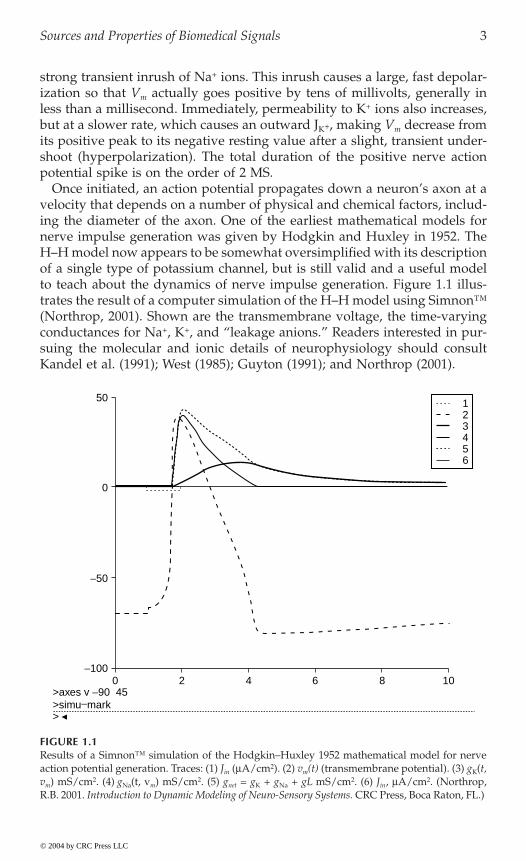
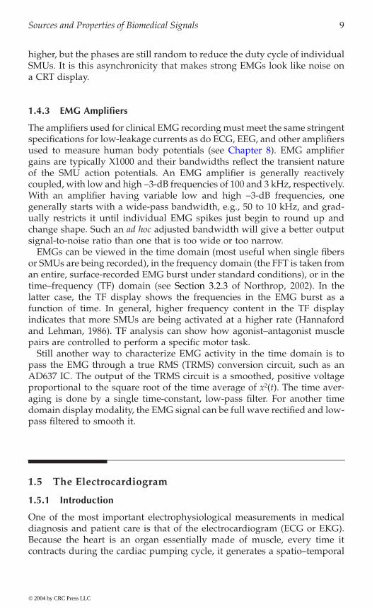
Once initiated, an action potential propagates down a neuron’s axon at avelocity that depends on a number of physical and chemical factors, includ-ing the diameter of the axon. One of the earliest mathematical models fornerve impulse generation was given by Hodgkin and Huxley in 1952. TheH–H model now appears to be somewhat oversimplified with its descriptionof a single type of potassium channel, but is still valid and a useful modelto teach about the dynamics of nerve impulse generation. Figure 1.1 illus-trates the result of a computer simulation of the H–H model using Simnon™(Northrop, 2001). Shown are the transmembrane voltage, the time-varyingconductances for Na+, K+, and “leakage anions.” Readers interested in pur-suing the molecular and ionic details of neurophysiology should consultKandel et al. (1991); West (1985); Guyton (1991); and Northrop (2001).
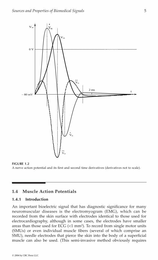
FIGURE 1.1Results of a Simnon™ simulation of the Hodgkin–Huxley 1952 mathematical model for nerveaction potential generation. Traces: (1) Jin (mA/cm2). (2) vm(t) (transmembrane potential). (3) gK(t,vm) mS/cm2. (4) gNa(t, vm) mS/cm2. (5) gnet = gK + gNa + gL mS/cm2. (6) Jin, mA/cm2. (Northrop,R.B. 2001. Introduction to Dynamic Modeling of Neuro-Sensory Systems. CRC Press, Boca Raton, FL.)
© 2004 by CRC Press LLC
50
0
−50
−1000 2 4 6 8 10
>axes v −90 45>simu−mark>
2
654
1
3
4 Analysis and Application of Analog Electronic Circuits
Most neurons in the vertebrate CNS are too small to record their trans-membrane potentials with glass micropipette electrodes directly. However,their action potentials can be recorded over long periods of time with extra-cellular, metal microelectrodes whose uninsulated tips are in the neuropilewithin several microns of axons or cell bodies. Action potentials from periph-eral nerve bundles can be recorded with simple platinum hook electrodes,saline-filled suction electrodes, or saline-wetted wick electrodes coupled tosilver–silver chloride electrodes. All extracellular recording techniques sufferfrom the problem that the electrodes pick up nerve spikes from active,adjacent, or neighboring neurons. This neural background noise is added tothe desired unit’s signal and, unfortunately, has the same bandwidth as thedesired unit’s spikes. In dissected peripheral nerve fibers, it may be possibleto isolate single axons with hook, suction, or wick electrodes, thus greatlyimproving the recording SNR.
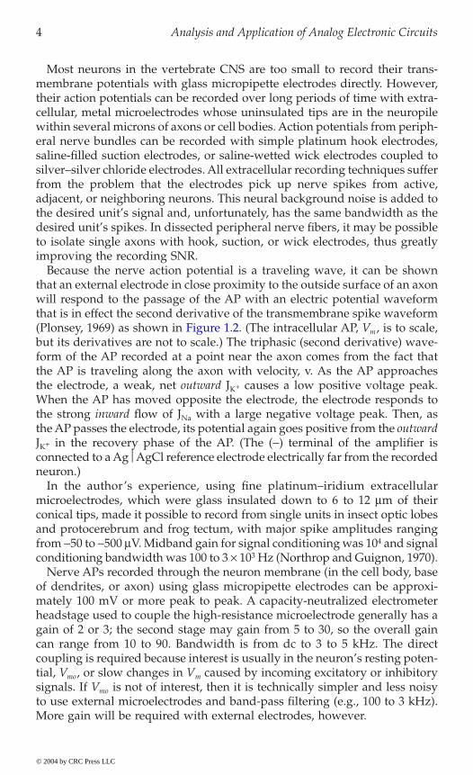
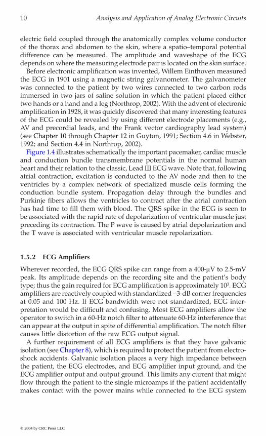
Because the nerve action potential is a traveling wave, it can be shownthat an external electrode in close proximity to the outside surface of an axonwill respond to the passage of the AP with an electric potential waveformthat is in effect the second derivative of the transmembrane spike waveform
m
but its derivatives are not to scale.) The triphasic (second derivative) wave-form of the AP recorded at a point near the axon comes from the fact thatthe AP is traveling along the axon with velocity, v. As the AP approachesthe electrode, a weak, net outward JK+ causes a low positive voltage peak.When the AP has moved opposite the electrode, the electrode responds tothe strong inward flow of JNa with a large negative voltage peak. Then, asthe AP passes the electrode, its potential again goes positive from the outwardJK+ in the recovery phase of the AP. (The (-) terminal of the amplifier isconnected to a AgΩAgCl reference electrode electrically far from the recordedneuron.)
In the author’s experience, using fine platinum–iridium extracellularmicroelectrodes, which were glass insulated down to 6 to 12 mm of theirconical tips, made it possible to record from single units in insect optic lobesand protocerebrum and frog tectum, with major spike amplitudes rangingfrom -50 to -500 mV. Midband gain for signal conditioning was 104 and signalconditioning bandwidth was 100 to 3 ¥ 103 Hz (Northrop and Guignon, 1970).
Nerve APs recorded through the neuron membrane (in the cell body, baseof dendrites, or axon) using glass micropipette electrodes can be approxi-mately 100 mV or more peak to peak. A capacity-neutralized electrometerheadstage used to couple the high-resistance microelectrode generally has again of 2 or 3; the second stage may gain from 5 to 30, so the overall gaincan range from 10 to 90. Bandwidth is from dc to 3 to 5 kHz. The directcoupling is required because interest is usually in the neuron’s resting poten-tial, Vmo, or slow changes in Vm caused by incoming excitatory or inhibitorysignals. If Vmo is not of interest, then it is technically simpler and less noisyto use external microelectrodes and band-pass filtering (e.g., 100 to 3 kHz).More gain will be required with external electrodes, however.
© 2004 by CRC Press LLC
(Plonsey, 1969) as shown in Figure 1.2. (The intracellular AP, V , is to scale,
Sources and Properties of Biomedical Signals 5
1.4 Muscle Action Potentials
1.4.1 Introduction
An important bioelectric signal that has diagnostic significance for manyneuromuscular diseases is the electromyogram (EMG), which can berecorded from the skin surface with electrodes identical to those used forelectrocardiography, although in some cases, the electrodes have smallerareas than those used for ECG (<1 mm2). To record from single motor units(SMUs) or even individual muscle fibers (several of which comprise anSMU), needle electrodes that pierce the skin into the body of a superficialmuscle can also be used. (This semi-invasive method obviously requires
FIGURE 1.2A nerve action potential and its first and second time derivatives (derivatives not to scale).
•Vm
Vm
• •
Vm
− 80 mV
Vm
t2 ms
•
Vm
• •
Vm
0 V
© 2004 by CRC Press LLC
6 Analysis and Application of Analog Electronic Circuits
sterile technique.) EMG recording is used to diagnose some causes of muscleweakness or paralysis, muscle or motor problems such as tremor or twitch-ing, motor nerve damage from injury or osteoarthritis, and pathologiesaffecting motor end plates.
1.4.2 The Origin of EMGs
There are several types of muscle in the body, e.g., striated, cardiac, andsmooth. Striated muscle in mammals can be further subdivided into fast andslow muscles (Guyton, 1991). Fast muscles are used for fast movements; theyinclude the two gastrocnemii, laryngeal muscles, extraocular muscles, etc.Slow muscles are used for postural control against gravity and include thesoleus; abdominal, back, and neck muscles; etc. EMG recording is generallycarried out on both types of skeletal muscles. It can also be done on lesssuperficial muscles such as the extraocular muscles that move the eyeballs,the eyelid muscles, and the muscles that work the larynx.
A particular striated muscle is innervated by a group of motor neuronsthat have origin at a certain level in the spinal cord. In the spinal cord, motorneurons receive excitatory and inhibitory inputs from motor control neuronsfrom the CNS, as well as excitatory and inhibitory inputs from local feedbackneurons from muscle spindles (responding to muscle length, x, and dx/dt),Golgi tendon organs (responding to muscle tension), and Renshaw feedbackcells (Northrop, 1999; Guyton, 1991). Individual motor neuron axons con-trolling the contraction of a particular striated muscle innervate small groupsof muscle fibers in the muscle called a single motor unit (SMU). Many SMUscomprise the entire muscle. The synaptic connections between the terminalbranches of a single motor neuron axon and its SMU fibers are called motorend plates (MEPs). MEPs are chemical synapses in which the neurotransmit-ter, acetylcholine (ACh), is released presynaptically and then diffuses acrossthe synaptic cleft or gap to ACh receptors on the subsynaptic membrane.
When a motor neuron action potential arrives at an MEP, it triggers theexocytosis or emptying of about 300 presynaptic vesicles containing ACh.(Approximately 3 ¥ 105 vesicles are in the terminals of a single MEP; eachvesicle is about 40 nm in diameter.) Some 107 to 5 ¥ 108 molecules of AChare needed to trigger a muscle action potential (Katz, 1966). The ACh diffusesacross the 20 to 30 nm synaptic cleft in approximately 0.5 MS; here someACh molecules combine with receptor sites on the protein subunits formingthe subsynaptic, ion-gating channels. Five high molecular weight proteinsubunits form each ion channel. ACh binding to the protein subunits triggersa dilation of the channel to approximately 0.65 nm. The dilated channelsallow Na+ ions to pass inward; however, Cl– is repelled by the fixed negativecharges on the mouth of the channel.
Thus, the subsynaptic membrane is depolarized by the inward JNa (i.e., itstransmembrane potential goes positive from the approximately -85 mV rest-ing potential), triggering a muscle action potential. The local subsynaptic
© 2004 by CRC Press LLC
Sources and Properties of Biomedical Signals 7
transmembrane potential can go to as much as +50 mV, forming an end platepotential (EPP) spike fused to the muscle action potential it triggers with aduration of approximately 8 MS, much longer than a nerve action potential.The ACh in the cleft and bound to the receptors is rapidly broken down(hydrolized) by the enzyme cholinesterase resident in the cleft, and its molec-ular components are recycled. A small amount of ACh also escapes the cleftby diffusion and is hydrolyzed as well.
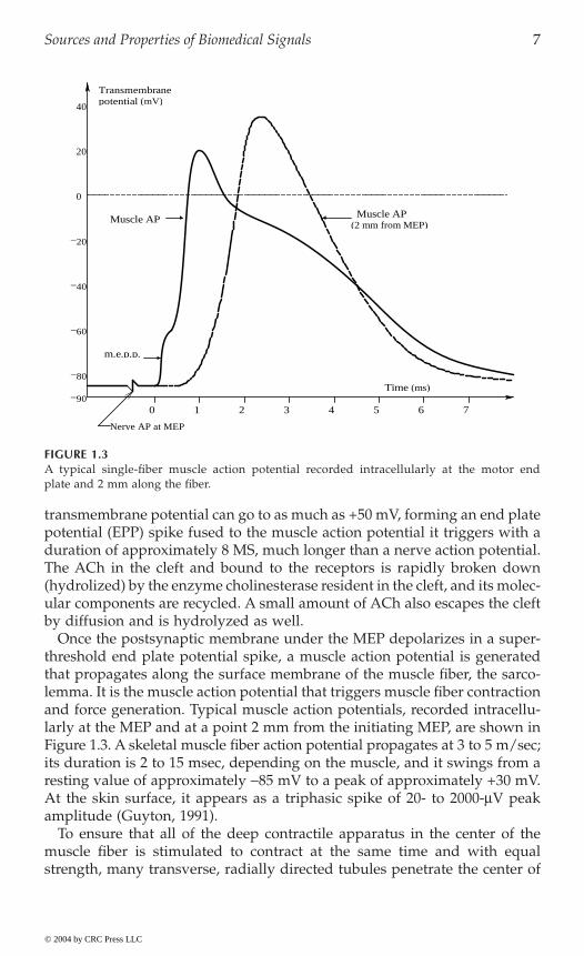
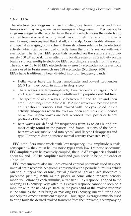
Once the postsynaptic membrane under the MEP depolarizes in a super-threshold end plate potential spike, a muscle action potential is generatedthat propagates along the surface membrane of the muscle fiber, the sarco-lemma. It is the muscle action potential that triggers muscle fiber contractionand force generation. Typical muscle action potentials, recorded intracellu-larly at the MEP and at a point 2 mm from the initiating MEP, are shown inFigure 1.3. A skeletal muscle fiber action potential propagates at 3 to 5 m/sec;its duration is 2 to 15 msec, depending on the muscle, and it swings from aresting value of approximately -85 mV to a peak of approximately +30 mV.At the skin surface, it appears as a triphasic spike of 20- to 2000-mV peakamplitude (Guyton, 1991).
To ensure that all of the deep contractile apparatus in the center of themuscle fiber is stimulated to contract at the same time and with equalstrength, many transverse, radially directed tubules penetrate the center of
FIGURE 1.3A typical single-fiber muscle action potential recorded intracellularly at the motor endplate and 2 mm along the fiber.
−90
−80
−60
−40
−20
0
20
40
0 1 2 3 4 5 6 7
m.e.p.p.
Time (ms)
Nerve AP at MEP
Muscle AP Muscle AP(2 mm from MEP)
Transmembranepotential (mV)
© 2004 by CRC Press LLC
8 Analysis and Application of Analog Electronic Circuits
the fiber along its length. These T-tubules are open to the extracellular fluidspace, as is the surface of the fiber, and they are connected to the surfacemembrane at both ends. The T-tubules conduct the muscle action potentialinto the interior of the fiber in many locations along its length.
Running longitudinally around the outsides of the contractile myofibrilsthat make up the fiber are networks of tubules called the sarcoplasmic retic-ulum (SR). Note that the terminal cisternae of the SR butt against the mem-brane of the T-tubes. When the muscle action potential penetrates along theT-tubes, the depolarization triggers the cisternae to release calcium ions intothe space surrounding the myofibrils’ contractile proteins. The Ca++ bindsto the protein troponin C, which triggers contraction by the actin and myosinproteins. (The molecular biophysics of the actual contraction process willnot be discussed here.)
A synchronous stimulation of all of the motor neurons innervating a muscleproduces what is called a muscle twitch; i.e., the tension initially falls a slightamount, rises abruptly, and then falls more slowly to zero again. Sustainedmuscle contraction is caused by a steady (average) rate of (asynchronous)motoneuron firing. When the firing ceases, the muscle relaxes.
Muscle relaxation is actually an active process. Calcium ion pumps locatedin the membranes of the SR longitudinal tubules actively transfer Ca++ fromoutside the tubules to inside the SR system. The lack of Ca++ in proximityto troponin C allows relaxation to occur. In resting muscle, the concentration,[Ca++], is about 10-7 M in the myofibrillar fluid (Guyton, 1991). In a twitch,[Ca++] rises to approximately 2 ¥ 10-5 M and, in a tetanic stimulation, [Ca++]is about 2 ¥ 10-4 M. The Ca++ released by a single motor nerve impulse istaken up by the SR pumps to restore the resting [Ca++] level in about 50 msec.
Just as in the case of the sodium pumps in nerve cell membrane, themuscles’ Ca++ pumps require metabolic energy to operate; adenosine tri-phosphate (ATP) is cleaved to the diphosphate to release the energy neededto drive the Ca++ pumps. The pumps can concentrate the Ca++ to approxi-mately 10-3 M inside the SR. Inside the SR tubules and cisternae, the Ca++ isstored in readily available ionic form, and as a protein chelate, bound to aprotein, calsequestrin.
So far, the events associated with a single muscle fiber have been described.As noted earlier, small groups of fibers innervated by a single motoneuronfiber are called a single motor unit (SMU). In muscles used for fine actions,such as those operating the fingers or tongue, fewer muscle fibers, or, equiv-alently, more motoneuron fibers per total number of muscle fibers, are in amotor unit. For example, the laryngeal muscles used for speech have onlytwo or three fibers per SMU, while large muscles used for gross motions,such as the gastrocnemius, can have several hundred fibers per SMU (Guyton,1991). To make fine movements, only a few motoneurons fire out of the totalnumber innervating the muscle and these do not fire synchronously. Theirfiring phase is made random in order to produce smooth contraction. Atmaximum tetanic stimulation, the mean frequency on the motoneurons is
© 2004 by CRC Press LLC
Sources and Properties of Biomedical Signals 9
higher, but the phases are still random to reduce the duty cycle of individualSMUs. It is this asynchronicity that makes strong EMGs look like noise ona CRT display.
1.4.3 EMG Amplifiers
The amplifiers used for clinical EMG recording must meet the same stringentspecifications for low-leakage currents as do ECG, EEG, and other amplifiers
gains are typically X1000 and their bandwidths reflect the transient natureof the SMU action potentials. An EMG amplifier is generally reactivelycoupled, with low and high -3-dB frequencies of 100 and 3 kHz, respectively.With an amplifier having variable low and high -3-dB frequencies, onegenerally starts with a wide-pass bandwidth, e.g., 50 to 10 kHz, and grad-ually restricts it until individual EMG spikes just begin to round up andchange shape. Such an ad hoc adjusted bandwidth will give a better outputsignal-to-noise ratio than one that is too wide or too narrow.
EMGs can be viewed in the time domain (most useful when single fibersor SMUs are being recorded), in the frequency domain (the FFT is taken froman entire, surface-recorded EMG burst under standard conditions), or in the
latter case, the TF display shows the frequencies in the EMG burst as afunction of time. In general, higher frequency content in the TF displayindicates that more SMUs are being activated at a higher rate (Hannafordand Lehman, 1986). TF analysis can show how agonist–antagonist musclepairs are controlled to perform a specific motor task.
Still another way to characterize EMG activity in the time domain is topass the EMG through a true RMS (TRMS) conversion circuit, such as anAD637 IC. The output of the TRMS circuit is a smoothed, positive voltageproportional to the square root of the time average of x2(t). The time aver-aging is done by a single time-constant, low-pass filter. For another timedomain display modality, the EMG signal can be full wave rectified and low-pass filtered to smooth it.
1.5 The Electrocardiogram
1.5.1 Introduction
One of the most important electrophysiological measurements in medicaldiagnosis and patient care is that of the electrocardiogram (ECG or EKG).Because the heart is an organ essentially made of muscle, every time itcontracts during the cardiac pumping cycle, it generates a spatio–temporal
© 2004 by CRC Press LLC
used to measure human body potentials (see Chapter 8). EMG amplifier
time–frequency (TF) domain (see Section 3.2.3 of Northrop, 2002). In the
10 Analysis and Application of Analog Electronic Circuits
electric field coupled through the anatomically complex volume conductorof the thorax and abdomen to the skin, where a spatio–temporal potentialdifference can be measured. The amplitude and waveshape of the ECGdepends on where the measuring electrode pair is located on the skin surface.
Before electronic amplification was invented, Willem Einthoven measuredthe ECG in 1901 using a magnetic string galvanometer. The galvanometerwas connected to the patient by two wires connected to two carbon rodsimmersed in two jars of saline solution in which the patient placed eithertwo hands or a hand and a leg (Northrop, 2002). With the advent of electronicamplification in 1928, it was quickly discovered that many interesting featuresof the ECG could be revealed by using different electrode placements (e.g.,AV and precordial leads, and the Frank vector cardiography lead system)
1992; and Section 4.4 in Northrop, 2002).
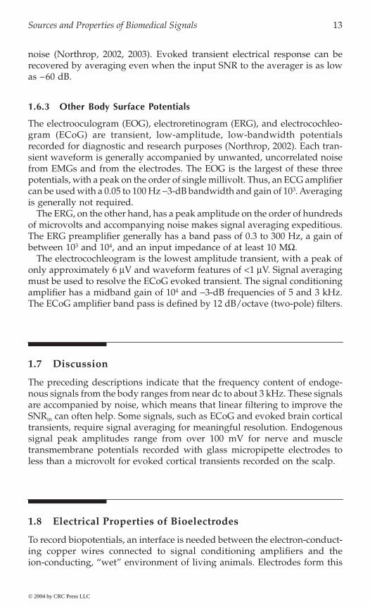
and conduction bundle transmembrane potentials in the normal humanheart and their relation to the classic, Lead III ECG wave. Note that, followingatrial contraction, excitation is conducted to the AV node and then to theventricles by a complex network of specialized muscle cells forming theconduction bundle system. Propagation delay through the bundles andPurkinje fibers allows the ventricles to contract after the atrial contractionhas had time to fill them with blood. The QRS spike in the ECG is seen tobe associated with the rapid rate of depolarization of ventricular muscle justpreceding its contraction. The P wave is caused by atrial depolarization andthe T wave is associated with ventricular muscle repolarization.
1.5.2 ECG Amplifiers
Wherever recorded, the ECG QRS spike can range from a 400-mV to 2.5-mVpeak. Its amplitude depends on the recording site and the patient’s bodytype; thus the gain required for ECG amplification is approximately 103. ECGamplifiers are reactively coupled with standardized -3-dB corner frequenciesat 0.05 and 100 Hz. If ECG bandwidth were not standardized, ECG inter-pretation would be difficult and confusing. Most ECG amplifiers allow theoperator to switch in a 60-Hz notch filter to attenuate 60-Hz interference thatcan appear at the output in spite of differential amplification. The notch filtercauses little distortion of the raw ECG output signal.
A further requirement of all ECG amplifiers is that they have galvanic
shock accidents. Galvanic isolation places a very high impedance betweenthe patient, the ECG electrodes, and ECG amplifier input ground, and theECG amplifier output and output ground. This limits any current that mightflow through the patient to the single microamps if the patient accidentallymakes contact with the power mains while connected to the ECG system
© 2004 by CRC Press LLC
Figure 1.4 illustrates schematically the important pacemaker, cardiac muscle
isolation (see Chapter 8), which is required to protect the patient from electro-
(see Chapter 10 through Chapter 12 in Guyton, 1991; Section 4.6 in Webster,

Sources and Properties of Biomedical Signals 11
and otherwise not grounded. Other biopotential amplifiers used in a clinicalor research setting with humans, such as for measurement of EEG, EMG,ERG, ECoG, etc., must also have galvanic isolation.
1.6 Other Biopotentials
1.6.1 Introduction
Many other biopotentials are measured for research and clinical purposes.These include the electroencephalogram (EEG); electroretinogram (ERG);electrooculogram (EOG); and electrocochleogram (ECoG) (Northrop, 2002).All of these signals are low amplitude (hundreds of microvolts at peak) andcontain primarily low frequencies (0.01 to 100 Hz).
FIGURE 1.4Schematic cut-away of a mammalian heart showing the SA and AV node pacemakers,as well as intracellular action potentials from different locations in the heart. Bottomtrace is a typical lead III skin surface-recorded ECG waveform.
LV
Action potentials
Q
R
STP
Purkinje fiber AP
SA node
Bundle branch AP
Common bundle AP
Atrial muscle AP
SA node AP
AV node AP
RV
- 90 mV
ca. 1 sec
AV node
Delays inconductionbundles
t
LA
RA
0
(Lead III)ECG
> 150 V/sec.
0 mVVentricular AP
Sup. vena cava
+20 mV
- 90 mV
-95 mV
© 2004 by CRC Press LLC
12 Analysis and Application of Analog Electronic Circuits
1.6.2 EEGs
The electroencephalogram is used to diagnose brain injuries and braintumors noninvasively, as well as in neuropsychology research. Electroenceph-alograms are generally recorded from the scalp, which means the underlying,cortical brain electrical activity must pass through the pia and dura matermembranes, cerebrospinal fluid, skull, and scalp. Considerable attenuationand spatial averaging occurs due to these structures relative to the electricalactivity, which can be recorded directly from the brain’s surface with wickelectrodes. The largest EEG potentials recorded on the scalp are approxi-mately 150 mV at peak. In an attempt to localize sites of EEG activity on thebrain’s surface, multiple electrode EEG recordings are made from the scalp.The standard 10 to 20 EEG electrode array uses 19 electrodes; some electrodearrays used in brain research use 128 electrodes (Northrop, 2002).EEGs have traditionally been divided into four frequency bands:
• Delta waves have the largest amplitudes and lowest frequencies(£3.5 Hz); they occur in adults in deep sleep.
• Theta waves are large-amplitude, low-frequency voltages (3.5 to7.5 Hz) and are seen in sleep in adults and in prepubescent children.
• The spectra of alpha waves lie between 7.5 and 13 Hz and theiramplitudes range from 20 to 200 mV. Alpha waves are recorded fromadults who are conscious but relaxed with the eyes closed. Alphaactivity disappears when the eyes are open and the subject focuseson a task. Alpha waves are best recorded from posterior lateralportions of the scalp.
• Beta waves are defined for frequencies from 13 to 50 Hz and aremost easily found in the parietal and frontal regions of the scalp.Beta waves are subdivided into types I and II: type I disappears andtype II appears during intense mental activity (Webster, 1992).
EEG amplifiers must work with low-frequency, low amplitude signals;consequently, they must be low noise types with low 1/f noise spectrums.EEG amplifiers can be reactively coupled; their –3-dB frequencies should beabout 0.2 and 100 Hz. Amplifier midband gain needs to be on the order of104 to 105.
EEG measurement also includes evoked cortical potentials used in exper-imental brain research. A patient is presented with a periodic stimulus, whichcan be auditory (a click or tone), visual (a flash of light or a tachistoscopicallypresented picture), tactile (a pin prick), or some other transient sensorymodality. Following each stimulus, a transient EEG response is added to theongoing EEG activity. Very often this evoked response cannot be seen on amonitor with the naked eye. Because the pass band of the evoked responseis the same as the interfering or masking EEG activity, linear filtering doesnot help in extracting transient response. Thus, signal averaging must be usedto bring forth the desired evoked transient from the unrelated, accompanying
© 2004 by CRC Press LLC
Sources and Properties of Biomedical Signals 13
noise (Northrop, 2002, 2003). Evoked transient electrical response can berecovered by averaging even when the input SNR to the averager is as lowas -60 dB.
1.6.3 Other Body Surface Potentials
The electrooculogram (EOG), electroretinogram (ERG), and electrocochleo-gram (ECoG) are transient, low-amplitude, low-bandwidth potentialsrecorded for diagnostic and research purposes (Northrop, 2002). Each tran-sient waveform is generally accompanied by unwanted, uncorrelated noisefrom EMGs and from the electrodes. The EOG is the largest of these threepotentials, with a peak on the order of single millivolt. Thus, an ECG amplifiercan be used with a 0.05 to 100 Hz -3-dB bandwidth and gain of 103. Averagingis generally not required.
The ERG, on the other hand, has a peak amplitude on the order of hundredsof microvolts and accompanying noise makes signal averaging expeditious.The ERG preamplifier generally has a band pass of 0.3 to 300 Hz, a gain ofbetween 103 and 104, and an input impedance of at least 10 MW.
The electrocochleogram is the lowest amplitude transient, with a peak ofonly approximately 6 mV and waveform features of <1 mV. Signal averagingmust be used to resolve the ECoG evoked transient. The signal conditioningamplifier has a midband gain of 104 and -3-dB frequencies of 5 and 3 kHz.The ECoG amplifier band pass is defined by 12 dB/octave (two-pole) filters.
1.7 Discussion
The preceding descriptions indicate that the frequency content of endoge-nous signals from the body ranges from near dc to about 3 kHz. These signalsare accompanied by noise, which means that linear filtering to improve theSNRin can often help. Some signals, such as ECoG and evoked brain corticaltransients, require signal averaging for meaningful resolution. Endogenoussignal peak amplitudes range from over 100 mV for nerve and muscletransmembrane potentials recorded with glass micropipette electrodes toless than a microvolt for evoked cortical transients recorded on the scalp.
1.8 Electrical Properties of Bioelectrodes
To record biopotentials, an interface is needed between the electron-conduct-ing copper wires connected to signal conditioning amplifiers and theion-conducting, “wet” environment of living animals. Electrodes form this
© 2004 by CRC Press LLC
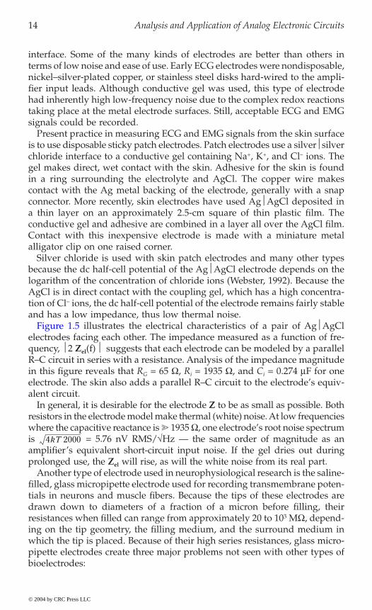
14 Analysis and Application of Analog Electronic Circuits
interface. Some of the many kinds of electrodes are better than others interms of low noise and ease of use. Early ECG electrodes were nondisposable,nickel–silver-plated copper, or stainless steel disks hard-wired to the ampli-fier input leads. Although conductive gel was used, this type of electrodehad inherently high low-frequency noise due to the complex redox reactionstaking place at the metal electrode surfaces. Still, acceptable ECG and EMGsignals could be recorded.
Present practice in measuring ECG and EMG signals from the skin surfaceis to use disposable sticky patch electrodes. Patch electrodes use a silverΩsilverchloride interface to a conductive gel containing Na+, K+, and Cl– ions. Thegel makes direct, wet contact with the skin. Adhesive for the skin is foundin a ring surrounding the electrolyte and AgCl. The copper wire makescontact with the Ag metal backing of the electrode, generally with a snapconnector. More recently, skin electrodes have used AgΩAgCl deposited ina thin layer on an approximately 2.5-cm square of thin plastic film. Theconductive gel and adhesive are combined in a layer all over the AgCl film.Contact with this inexpensive electrode is made with a miniature metalalligator clip on one raised corner.
Silver chloride is used with skin patch electrodes and many other typesbecause the dc half-cell potential of the AgΩAgCl electrode depends on thelogarithm of the concentration of chloride ions (Webster, 1992). Because theAgCl is in direct contact with the coupling gel, which has a high concentra-tion of Cl- ions, the dc half-cell potential of the electrode remains fairly stableand has a low impedance, thus low thermal noise.
electrodes facing each other. The impedance measured as a function of fre-quency, Ω2 Zel(f) Ω suggests that each electrode can be modeled by a parallelR–C circuit in series with a resistance. Analysis of the impedance magnitudein this figure reveals that RG = 65 W, Ri = 1935 W, and Ci = 0.274 mF for oneelectrode. The skin also adds a parallel R–C circuit to the electrode’s equiv-alent circuit.
In general, it is desirable for the electrode Z to be as small as possible. Bothresistors in the electrode model make thermal (white) noise. At low frequencieswhere the capacitive reactance is 1935 W, one electrode’s root noise spectrumis = 5.76 nV RMS/÷Hz — the same order of magnitude as anamplifier’s equivalent short-circuit input noise. If the gel dries out duringprolonged use, the Zel will rise, as will the white noise from its real part.
Another type of electrode used in neurophysiological research is the saline-filled, glass micropipette electrode used for recording transmembrane poten-tials in neurons and muscle fibers. Because the tips of these electrodes aredrawn down to diameters of a fraction of a micron before filling, theirresistances when filled can range from approximately 20 to 103 MW, depend-ing on the tip geometry, the filling medium, and the surround medium inwhich the tip is placed. Because of their high series resistances, glass micro-pipette electrodes create three major problems not seen with other types ofbioelectrodes:
4kT 2000
© 2004 by CRC Press LLC
Figure 1.5 illustrates the electrical characteristics of a pair of AgΩAgCl
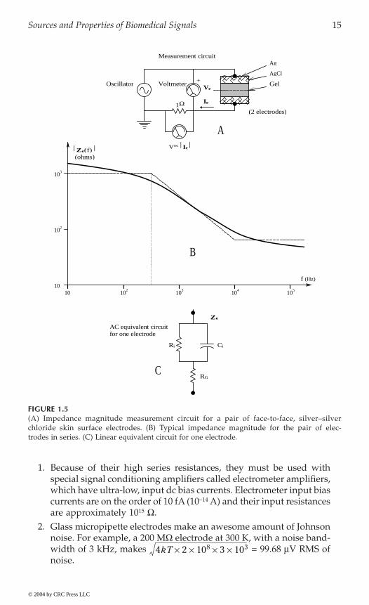
Sources and Properties of Biomedical Signals 15
1. Because of their high series resistances, they must be used withspecial signal conditioning amplifiers called electrometer amplifiers,which have ultra-low, input dc bias currents. Electrometer input biascurrents are on the order of 10 fA (10-14 A) and their input resistancesare approximately 1015 W.
2. Glass micropipette electrodes make an awesome amount of Johnsonnoise. For example, a 200 MW electrode at 300 K, with a noise band-width of 3 kHz, makes = 99.68 mV RMS ofnoise.
FIGURE 1.5(A) Impedance magnitude measurement circuit for a pair of face-to-face, silver–silverchloride skin surface electrodes. (B) Typical impedance magnitude for the pair of elec-trodes in series. (C) Linear equivalent circuit for one electrode.
1Ω
Gel
AgCl
Ag
(2 electrodes)
f (Hz)
Ri Ci
Ze
B
Ze(f)(ohms)
10 102 103 104 105
Measurement circuit
RG
Ie
V∝Ie
VoltmeterOscillatorVe
+
103
102
10
C
AC equivalent circuitfor one electrode
A
4kT 2 108 3 103¥¥¥¥
© 2004 by CRC Press LLC

16 Analysis and Application of Analog Electronic Circuits
3.capacitance between the electrolyte inside and the electrolyte outsidethe tip (see Figure 1.6), which makes them behave like distributed-
This figure also illustrates the equivalent circuits of the AgΩAgCl couplingelectrodes, the cell membrane, and the microelectrode tip spreading resis-tance and tip EMF. The distributed resistance of the internal electrolyte inthe tip, Rtip, plus the tip spreading resistance, Rtc, plus the cell membrane’sresistance, 1/Gc, are orders of magnitude larger than the impedances asso-ciated with the AgCl coupling electrodes. Thus, they can be lumped togetheras a single Rm and the distributed tip capacitance can be represented by asingle, lumped Cm in the simplified R–C LPF of Figure 1.7(B). Vbio is thebioelectric EMF across the cell membrane in the vicinity of the microelectrodetip. The break frequency of the B circuit is simply fb = 1/(2pRmCm) Hz.
FIGURE 1.6Schematic cross section (not to scale) of an electrolyte-filled, glass micropipette electrodeinserted into the cytoplasm of a cell. AgΩAgCl electrodes are used to interface recordingwires (generally Cu) with the electrolytes.
+++
++
+
++ + + +
+
++
+
+
++ + + + +
+
−
+ −−
−−
−
−− −
− −++ −− − −
−−−
−−
−−
−+ +−
AgClelectrode
Fillingelectrolyte
EA
CN
Vo
Shuntingcapacitance
External
++ −
−AgClelectrode+−
−−
Cell cytoplasm
Nucleus
Extracellularelectrolyte
Tip resistance
Glass tube R
E
Cell membrane
© 2004 by CRC Press LLC
parameter low-pass filters, as shown in Figure 1.7(A).
The tips of glass micropipette electrodes have significant distributed

Sources and Properties of Biomedical Signals 17
Typical values of circuit parameters are Rm @ 2 ¥ 108 W, Cm @ 1 ¥ 10-12 F.Thus fb @ 796 Hz. This is too low a break frequency to reproduce a nerveaction potential faithfully, which requires at least a dc to 3-kHz bandwidth.To obtain the desired bandwidth, capacitance neutralization is used (capac-
the amplifier output.
1.9 Exogenous Bioelectric Signals
The preceding sections have shown that endogenous bioelectric signals areinvariably small, ranging from single microvolts to over 100 mV. Their band-widths range from dc to perhaps 10 kHz at the most. Signals such as ECG
FIGURE 1.7(A) Equivalent circuit of an intracellular glass microelectrode in a cell, including theequivalent circuits of the AgΩAgCl electrodes. Note the dc half-cell potentials of theelectrodes and at the microelectrode’s tip. The tip of the microelectrode is modeled bya lumped-parameter, nonuniform, R–C transmission line. (B) For practical purposes, theac equivalent circuit of the glass micropipette electrode is generally reduced to a simpleR–C low-pass filter.
+
+
Gc
Etip
Im∆Ctipk
Rtip
Rse
Rse
Rpe
Cpe(E)
(E)
(R)
(R)
Cµ
Rµ
Cc
Vbio
B
Ve
Rtc
Ve
Eel
Eel
A+(Outside cell)
Cpe
+
+
Rpe −
(Inside cell)
−
© 2004 by CRC Press LLC
itance neutralization is described in Section 4.5.2 of Chapter 4). As shownin Section 9.8.4 in Chapter 9, capacitance neutralization adds excess noise to

18 Analysis and Application of Analog Electronic Circuits
and EEG require approximately 0.1 to 100 Hz. Exogenous signals on theother hand, can involve modalities such as ultrasound, which can use fre-quencies from hundreds of kilohertz to tens of megahertz, depending on theapplication. Ultrasound can be continuous wave (CW) sinusoidal, sinusoidalpulses, or wavelets. The purpose here is not to discuss the details of howultrasound is generated, received, or processed, but rather to comment onthe frequencies and signal levels of the received ultrasound.
Reflected ultrasound is picked up by a piezoelectric transducer or trans-ducer array that converts the mechanical sound pressure waves at the skinsurface to electrical currents or voltages. Concern for damaging tissues withthe transmitted ultrasound intensity (cells destroyed by heating or cavita-tion) means that input sound intensity must be kept low enough to be safefor living tissues, organs, fetuses, etc., yet high enough to give a good outputsignal SNR from the reflected sound energy impinging on the receivingtransducer. Many ultrasound transducers are used at ultrasound frequenciesbelow their mechanical resonance.
In this region of operation, the transducer has an equivalent circuitx
course depends on thickness, dielectric constant of its material, and area ofthe metal film electrodes; Cx is generally on the order of hundreds of pico-farads. Gx is the leakage conductance of the piezomaterial and also dependson the material and its dimensions. Expect Gx on the order of 10-13 S. Thecoaxial cable connecting the transducer to the charge amplifier has someshunt capacitance, Cc, which depends on cable length and insulating mate-rial; it will be on the order of approximately 30 pF/m. Similarly, the cablehas some leakage conductance, Gc, which again is length and material depen-dent; Gc will be about 10-11 S. Finally, the input conductance and capacitanceof the electrometer op amp are about Gi = 10-14 S and Ci = 3 pF.
The circuit of Figure 1.8 is a charge amplifier, which effectively replaces(Cx + Cc + Ci) and (Gx + Gc + Gi) with CF and GF in parallel with the trans-ducer’s Norton current source. Thus the low-frequency behavior of the sys-tem is not set by the poorly defined (Cx + Cc + Ci) and (Gx + Gc + Gi) butrather by the designer-specified components GF and CF. (Analysis of the
Norton current source, ix, is proportional to the rate of change of the ultra-sound pressure waves impingent on the bottom of the transducer. The con-stant d has the dimensions of coulombs/newton. The charge displaced insidethe transducer is given by q = d F. The Norton current is simply ix ∫
·q = d ·F =d
·PA. If the op amp is assumed to be ideal, then the summing junction is at0 V and, by Ohm’s law, the op amp’s output voltage is
(1.2)VdAsP ssC Go
F F
= ( )+
© 2004 by CRC Press LLC
described by Figure 1.8. C is the capacitance of the transducer, which of
circuit is carried out in detail in Section 6.6.3 of Chapter 6.) Note that the
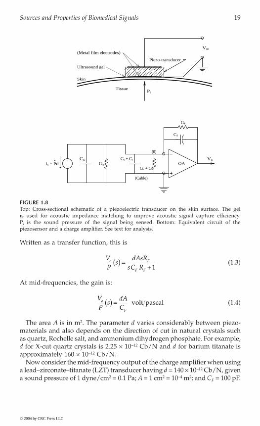
Sources and Properties of Biomedical Signals 19
Written as a transfer function, this is
(1.3)
At mid-frequencies, the gain is:
(1.4)
The area A is in m2. The parameter d varies considerably between piezo-materials and also depends on the direction of cut in natural crystals suchas quartz, Rochelle salt, and ammonium dihydrogen phosphate. For example,d for X-cut quartz crystals is 2.25 ¥ 10-12 Cb/N and d for barium titanate isapproximately 160 ¥ 10-12 Cb/N.
Now consider the mid-frequency output of the charge amplifier when usinga lead–zirconate–titanate (LZT) transducer having d = 140 ¥ 10-12 Cb/N, givena sound pressure of 1 dyne/cm2 = 0.1 Pa; A = 1 cm2 = 10-4 m2; and CF = 100 pF.
FIGURE 1.8Top: Cross-sectional schematic of a piezoelectric transducer on the skin surface. The gelis used for acoustic impedance matching to improve acoustic signal capture efficiency.Pi is the sound pressure of the signal being sensed. Bottom: Equivalent circuit of thepiezosensor and a charge amplifier. See text for analysis.
Gx
Gc + Gi
Cx Cc + Ci
GF
CF
Vo
Pi
Skin
Piezo-transducer
Ultrasound gel
Voc
Tissue
OA
(0)
(Cable)
•ix = Pd
(Metal film electrodes)
VP
sdAsR
sC Ro F
F F
( ) =+ 1
VP
sdAC
o
F
( ) = volt pascal
© 2004 by CRC Press LLC
20 Analysis and Application of Analog Electronic Circuits
(1.5)
Thus, received voltage levels in piezoelectric ultrasonic systems are verylow. Considerable low-noise amplification is required and band-pass filteringis necessary to improve signal-to-noise ratio. Not included in the precedinganalysis is the high-frequency response of the charge amplifier, which iscertainly important when conditioning low-level ultrasonic signals in the
ysis of the charge amplifier.)
1.10 Chapter Summary
This chapter has stressed that endogenous biomedical signals, whether elec-trical such as the ECG or EEG, or physical quantities such as blood pressureor temperature, vary relatively slowly; their signal bandwidths are generallyfrom dc to several hundred Hertz and, in the case of nerve spikes or EMGs,may require up to 2 to 4 kHz at the high end. All bioelectric signals arenoisy — that is, they are recorded in the company of broadband noise arisingfrom nearby physiological sources; in many cases (e.g., EEG, ERG, EOG, andECoG), they are in the microvolt range and must compete with amplifiernoise. In the case of a skin-surface EMG, the recorded signals are the spa-tio–temporal summation of many thousand individual sources underlyingthe electrodes, i.e., many muscle fibers asynchronously generating actionpotentials as they contract to do mechanical work. In the case of the scalp-recorded EEG, many millions of cortical neurons signal by spiking or byslow depolarization as the brain works, generating a spatio–temporallysummed potential between pairs of scalp electrodes.
On the other hand, the electrical activity from the heart is spatially local-ized. The synchronous spread of depolarization of cardiac muscle duringthe cardiac cycle generates a relatively strong signal on the skin surface, inspite of the large volume conductor volume through which the ECG electric
peak signal amplitudes and the approximate range of frequencies requiredto condition EOG, EEG, ECG, and EMG signals. Note that the waveformsthat contain spikes or sharp peak transients (ECG and EMG) require a higherbandwidth to characterize.
Exogenous biomedical instrumentation signals, such as diagnostic andDoppler ultrasound and signals from MRI systems, were shown to requirebandwidths into the tens of megahertz and higher. Amplifiers required forconditioning such exogenous signals must have high gain bandwidth prod-ucts (fT), and high slew rates (h), as well as low noise.
VPAdCo
F
= = ¥ ¥ ¥¥
=- -
-0 1 10 140 10
100 1014
4 12
12
. mV
© 2004 by CRC Press LLC
field must spread. Figure 1.9 illustrates the approximate extreme ranges of
range of megahertz. (See Section 6.6.3 in Chapter 6 for high-frequency anal-

Sources and Properties of Biomedical Signals 21
FIGURE 1.9Approximate RMS spectra of four classes of bioelectric signals. Peak expected RMS signal isplotted vs. extreme range of frequencies characterizing the signal.
f (Hz)
10−2
EMG
ECG
EEG
EOG10−4
10−3
10−1
10−5
0.1 1.0 10
10−2
102 103 104
Voltagerange
© 2004 by CRC Press LLC

23
2Models for Semiconductor Devices Used in Analog Electronic Systems
2.1 Introduction
This chapter will describe the properties and characteristics of the semicon-ductor components of analog integrated circuits (AICs). These includediodes, bipolar junction transistors (BJTs), and various types of field-effecttransistors (FETs). Biomedical engineers probably will never be called uponto design circuits with or use discrete transistors, with the possible exceptionof power transistors. Instead, modern analog electronic systems use inte-grated circuits. To appreciate the behavior and limitations of ICs, however,it is necessary to understand the fundamental behavior of their semiconduc-tor components. (The actual design of ICs is beyond the scope of this text.)One of the most ubiquitous analog ICs is the operational amplifier (op amp);op amps are used in many signal conditioning applications, including dif-ferential amplifiers; instrumentation amplifiers; active filters; true RMS con-verters; precision rectifiers; track-and-hold circuits; etc. Other commonlyencountered ICs in biomedical engineering are dc voltage regulators, tem-perature sensors, phase-lock loops, synchronous rectifiers, analog multipli-ers, dc-to-dc converters, medical isolation amplifiers, analog-to-digitalconverters (ADCs), digital-to-analog converters (DACs), etc.
Specifically, the following sections will examine the salient circuit charac-teristics of pn junction diodes, light-emitting diodes (LEDs), laser diodes(LADs), npn and pnp small-signal BJTs, junction field-effect transistors(JFETs), and n- and p-MOSFETs. Large-signal and mid- and high-frequencysmall-signal models will be considered. The mid- and high-frequency behav-ior of IC “building blocks” that use two transistors will also be analyzed.
© 2004 by CRC Press LLC
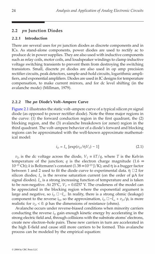
24 Analysis and Application of Analog Electronic Circuits
2.2 pn Junction Diodes
2.2.1 Introduction
There are several uses for pn junction diodes as discrete components and inICs. As stand-alone components, power diodes are used to rectify ac toproduce dc in power supplies. They are also used with inductive componentssuch as relay coils, motor coils, and loudspeaker windings to clamp inductivevoltage switching transients to prevent them from destroying the switchingtransistors. Small, discrete pn diodes are also used in op amp precisionrectifier circuits, peak detectors, sample-and-hold circuits, logarithmic ampli-fiers, and exponential amplifiers. Diodes are used in IC designs for temperaturecompensation, to make current mirrors, and for dc level shifting (in theavalanche mode) (Millman, 1979).
2.2.2 The pn Diode’s Volt–Ampere Curve
diode (as opposed to power rectifier diode). Note the three major regions inthe curve: (1) the forward conduction region in the first quadrant, the (2)blocking region, and the (3) avalanche breakdown (or zener) region in thethird quadrant. The volt–ampere behavior of a diode’s forward and blockingregions can be approximated with the well-known approximate mathemat-ical model:
iD = Irs [exp(vD/hVT) - 1] (2.1)
vD is the dc voltage across the diode, VT ∫ kT/q, where T is the Kelvintemperature of the junction; q is the electron charge magnitude (1.6 ¥10–19 Cb); k is Boltzmann’s constant (1.38 ¥ 10-23 J/K); and h is a bugger factorbetween 1 and 2 used to fit the diode curve to experimental data. h @ 2 forsilicon diodes; Irs is the reverse saturation current (on the order of mA forsignal diodes). Irs is a strong increasing function of temperature and is takento be non-negative. At 25∞C, VT = 0.0257 V. The crudeness of the model canbe appreciated in the blocking region where the exponential argument islarge and negative, so iD @ -Irs. In reality, there is a strong ohmic (leakage)component to the reverse iD, so the approximation, iD @ -Irs + vD/r, is morerealistic for vD < 0. r has the dimensions of resistance (ohms).
Avalanche occurs under reverse-biased conditions when minority carriersconducting the reverse iD gain enough kinetic energy by accelerating in thestrong electric field and, through collisions with the substrate atoms’ electrons,create new electron–hole pairs. These new carriers in turn are accelerated inthe high E-field and cause still more carriers to be formed. This avalancheprocess can be modeled by the empirical equation:
© 2004 by CRC Press LLC
Figure 2.1 illustrates the static volt–ampere curve of a typical silicon pn signal
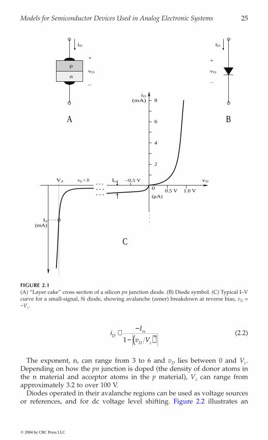
Models for Semiconductor Devices Used in Analog Electronic Systems 25
(2.2)
The exponent, n, can range from 3 to 6 and vD lies between 0 and Vz.Depending on how the pn junction is doped (the density of donor atoms inthe n material and acceptor atoms in the p material), Vz can range fromapproximately 3.2 to over 100 V.
Diodes operated in their avalanche regions can be used as voltage sources
FIGURE 2.1(A) “Layer cake” cross section of a silicon pn junction diode. (B) Diode symbol. (C) Typical I–Vcurve for a small-signal, Si diode, showing avalanche (zener) breakdown at reverse bias, vD =-Vz.
1.0 V0.5 V
−0.5 V
iD
(mA)
2
4
6
8
p
n
vD
vD vD
iD iD
++
− −
BA
. . .
(µA). . .
. . .VZ Irs
(mA)
.
.
.IZ
0
C
vD < 0
iI
v VD
rs
D z
n@
-
- ( )1
© 2004 by CRC Press LLC
or references, and for dc voltage level shifting. Figure 2.2 illustrates an

26 Analysis and Application of Analog Electronic Circuits
avalanche dc voltage source circuit. The tantalum filter capacitor is used tolower the source impedance of the avalanche supply at high frequencies.From Ohm’s law:
IL = VZ/RL (2.3)
IS = IL + IZ (2.4)
(2.5)
Every avalanche (zener) diode has a preferred operating point, (VZ, IZ),given by the manufacturer, at which its dynamic impedance is low andpower dissipation is safe. Thus in Equation 2.5 VZ and IZ are known and RL
is known (or IL at VZ), enabling one to find the required series RS. The requiredpower dissipated in RS is simply PRs = (VS - VZ)2/RS = IS
2 RS watts.Excluding the avalanche region, the dc characteristics of a pn junction
For the ideal diode, iD = 0 for vD < 0, and vD = 0 for iD > 0. Figure 2.3(B)shows that, by adding a reverse-biasing voltage source, VF, model diodevolt–ampere curve can be shifted to the right by VF . The model is made yetmore real by adding the series resistance, RF, in the conduction path, asshown in Figure 2.3(C). In Figure 2.3(D), a leakage conductance is added inparallel with the model of C to model reverse diode leakage.
The ideal diode and its variations are useful for pencil-and-paper circuitanalysis. Detailed simulation of electronic circuits containing diodes is donewith electronic circuit analysis programs (ECAPs) such as PSPICE and Micro-Cap, which handle the nonlinearity algebraically as well as compute thediode’s voltage-dependent shunt capacitance.
FIGURE 2.2Use of an avalanche (zener) diode as a DC voltage source for RL. The diode’s zener resistanceis neglected.
IZ
ILVZ
RL
VS
IS RS
R V V IV V
I V RS S Z SS Z
Z Z L
= -( ) =-( )
+
© 2004 by CRC Press LLC
diode can be modeled by an ideal diode (ID) model, shown in Figure 2.3(A).
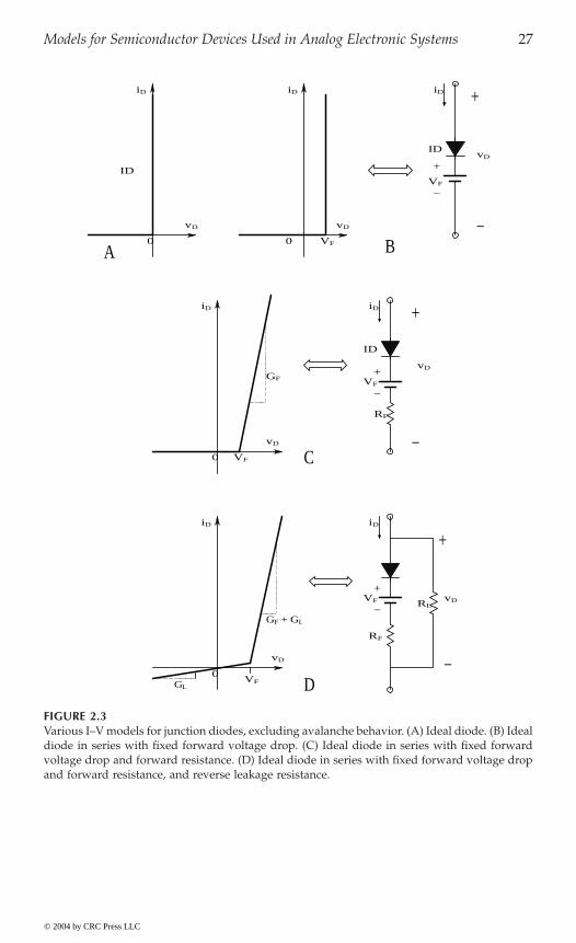
Models for Semiconductor Devices Used in Analog Electronic Systems 27
FIGURE 2.3Various I–V models for junction diodes, excluding avalanche behavior. (A) Ideal diode. (B) Idealdiode in series with fixed forward voltage drop. (C) Ideal diode in series with fixed forwardvoltage drop and forward resistance. (D) Ideal diode in series with fixed forward voltage dropand forward resistance, and reverse leakage resistance.
vD vD
vD
vD
iD iD
iD iD
iD iD iD
VF
VF
VF
ID
ID
+
vD
+
+
VF
+
vD
+
0 0
0
−
0
−
ID
−
−
−
VF
−
vD
+
GF
RF
RF
RL
GL
GF + GL
VF
D
C
A B
© 2004 by CRC Press LLC
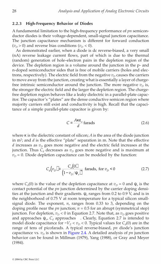
28 Analysis and Application of Analog Electronic Circuits
2.2.3 High-Frequency Behavior of Diodes
A fundamental limitation to the high-frequency performance of pn semicon-ductor diodes is their voltage-dependent, small-signal junction capacitance.The junction capacitance mechanism is different for forward conduction(vD > 0) and reverse bias conditions (vD < 0).
As demonstrated earlier, when a diode is dc reverse-biased, a very small(nA) reverse leakage current flows, part of which is due to the thermal(random) generation of hole–electron pairs in the depletion region of thedevice. The depletion region is a volume around the junction in the p- andn-doped semiconductor sides that is free of mobile carriers (holes and elec-trons, respectively). The electric field from the negative vD causes the carriersto move away from the junction, creating what is essentially a layer of charge-free intrinsic semiconductor around the junction. The more negative vD is,the stronger the electric field and the larger the depletion region. The charge-free depletion region behaves like a leaky dielectric in a parallel-plate capac-itor. The capacitor’s “plates” are the dense conductive semicon region wheremajority carriers still exist and conductivity is high. Recall that the capaci-tance of a simple parallel-plate capacitor is given by:
(2.6)
where k is the dielectric constant of silicon; A is the area of the diode junctionin m2; and d is the effective “plate” separation in m. Note that the effectived increases as vD goes more negative and the electric field increases at thejunction. Thus Cd decreases as vD goes more negative and is maximum atvD = 0. Diode depletion capacitance can be modeled by the function:
(2.7)
where Cd(0) is the value of the depletion capacitance at vD = 0 and yo is thecontact potential of the pn junction determined by the carrier doping densi-ties at the junction and their gradients. yo ranges from 0.2 to 0.9 V, and is inthe neighborhood of 0.75 V at room temperature for a typical silicon small-signal diode. The exponent, n, ranges from 0.33 to 3, depending on thedoping profile near the pn junction; n = 0.5 for an abrupt (symmetrical step)junction. For depletion, vD < 0 in Equation 2.7. Note that, as vD goes positiveand approaches yo, Cd approaches •. Clearly, Equation 2.7 is intended tomodel diode capacitance for -VZ < vD < 0. Typical values for Cd(0) are in therange of tens of picofarads. A typical reverse-biased, pn diode’s junction
D
behavior can be found in Millman (1979), Yang (1988), or Gray and Meyer(1984).
CA
do=
kefarads
C vC
vvd D
d
D o
n D( ) = ( )-( )
<0
10
y farads, for
© 2004 by CRC Press LLC
capacitance vs. v is shown in Figure 2.4. A detailed analysis of pn junction
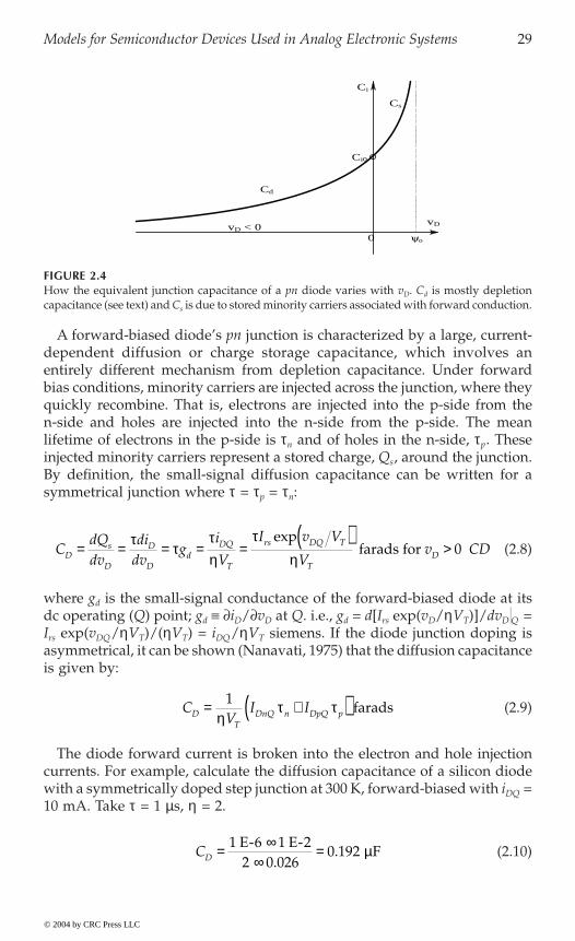
Models for Semiconductor Devices Used in Analog Electronic Systems 29
A forward-biased diode’s pn junction is characterized by a large, current-dependent diffusion or charge storage capacitance, which involves anentirely different mechanism from depletion capacitance. Under forwardbias conditions, minority carriers are injected across the junction, where theyquickly recombine. That is, electrons are injected into the p-side from then-side and holes are injected into the n-side from the p-side. The meanlifetime of electrons in the p-side is tn and of holes in the n-side, tp. Theseinjected minority carriers represent a stored charge, Qs, around the junction.By definition, the small-signal diffusion capacitance can be written for asymmetrical junction where t = tp = tn:
(2.8)
where gd is the small-signal conductance of the forward-biased diode at itsdc operating (Q) point; gd ∫ ∂iD/∂vD at Q. i.e., gd = d[Irs exp(vD/hVT)]/dvDQ =Irs exp(vDQ/hVT)/(hVT) = iDQ/hVT siemens. If the diode junction doping isasymmetrical, it can be shown (Nanavati, 1975) that the diffusion capacitanceis given by:
(2.9)
The diode forward current is broken into the electron and hole injectioncurrents. For example, calculate the diffusion capacitance of a silicon diodewith a symmetrically doped step junction at 300 K, forward-biased with iDQ =10 mA. Take t = 1 ms, h = 2.
(2.10)
FIGURE 2.4How the equivalent junction capacitance of a pn diode varies with vD. Cd is mostly depletioncapacitance (see text) and Cs is due to stored minority carriers associated with forward conduction.
Cj
Cd
Cs
vD
ψo0vD < 0
Cj0
CdQdv
didv
gi
V
I v V
Vv CDD
s
D
D
Dd
DQ
T
rs DQ T
TD= = = = =
( )>t t
th
th
exp farads for 0
CV
I IDT
DnQ n DpQ p= +( )1h
t t farads
CD = ¥¥
=1 1 22 0 026
0 192 E-6 E-
F.
. m
© 2004 by CRC Press LLC

30 Analysis and Application of Analog Electronic Circuits
This is a relatively enormous small-signal capacitance that appears inparallel with the diode model. The capacitance, CD, affects the speed at whichthe diode can turn off. However, the forward-biased diode has the timeconstant:
(2.11)
which is basically the mean minority carrier lifetime, t. Thus, CD has littleeffect on mid-frequency, small-signal performance, but the stored chargedoes affect the time to stop conducting when vD goes step negative.
forms in the n-material for a pn junction diode in which a step of forwardvoltage is followed by a step of reverse voltage. Note that VD remains at theforward value following switching to VR until all the excess minority carriershave been discharged from CD. Then VD Æ -VR and depletion capacitancedominates the junction behavior. The storage time is on the order of nano-seconds for most small-signal Si, pn diodes.
2.2.4 Schottky Diodes
The Schottky barrier diode (SBD), also called a hot carrier diode, consists of arectifying, metal insulator–semiconductor (MIS) junction. SBDs actually pre-date pn junction diodes by about 50 years. The first detectors in early crystalset radios were “cat’s whisker” diodes, in which a fine lead wire madecontact with a metallic mineral crystal, such as galena, silicon, or germanium.Such cat’s whisker detectors were, in fact, primitive SBDs. Because theirrectifier characteristics were not reproducible, cat’s whisker SBDs were onlysuited for early radio experimenters and were replaced by pn junction diodesin the 1950s.
The presence of a very thin, insulating interfacial oxide layer from 0.5 to1.5 nm thick between the metal and the semicon makes a modern SBD
shows the static I–V characteristics of a pn diode and an SBD. Note that theSBD has a lower cut-in voltage (approximately 0.3 V) than the pn diode(approximately 0.55 V) as well as about 1000 times the reverse leakagecurrent (0.1 mA vs. 1 nA), which does not saturate. A schematic cross sectionof an SBD (after Boylstead and Nashelsky, 1987) is shown on the figure.
The SBD is a majority carrier device; a pnD is a minority carrier device. Inorder for a pnD to block reverse current, the stored minority carriers mustbe swept out of the junction by the reverse electric field. This discharginglimits the turn-off time to microseconds. On the other hand, the SBD has no
a high-frequency SSM for the SBD when conducting. Note that the SS forward
t md D dC g= = ¥( )( ) @1 92 2 2 0 026 1. .E-7 1 E- s
© 2004 by CRC Press LLC
Figure 2.5 illustrates the current, voltage, and excess minority charge wave-
different from an ordinary ohmic, metal–semiconductor connection. Figure 2.6
minority carrier storage and can switch off in tens of nanoseconds, meaningthe SBD can rectify currents in the hundreds of megahertz. Figure 2.7 shows
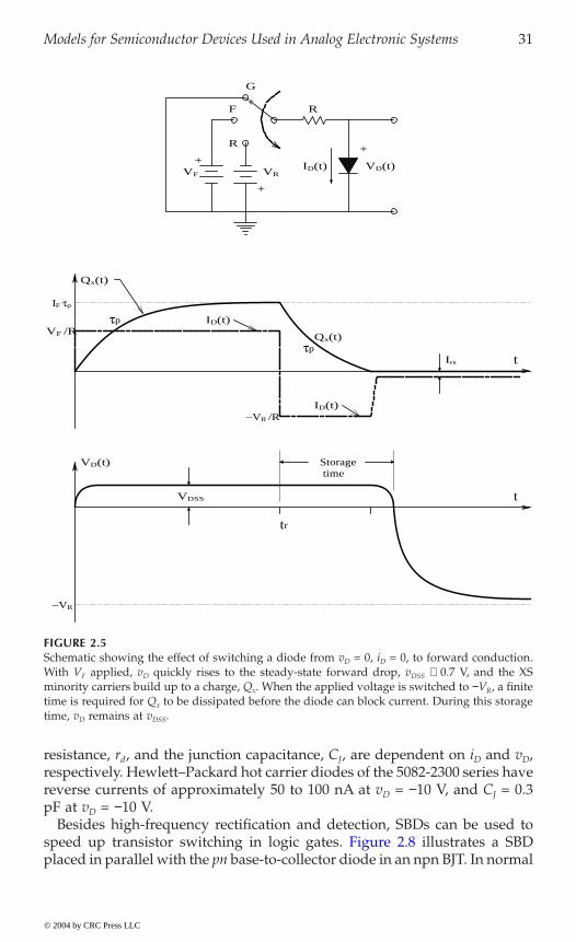
Models for Semiconductor Devices Used in Analog Electronic Systems 31
resistance, rd, and the junction capacitance, CJ, are dependent on iD and vD,respectively. Hewlett–Packard hot carrier diodes of the 5082-2300 series havereverse currents of approximately 50 to 100 nA at vD = -10 V, and CJ = 0.3pF at vD = -10 V.
Besides high-frequency rectification and detection, SBDs can be used to
placed in parallel with the pn base-to-collector diode in an npn BJT. In normal
FIGURE 2.5Schematic showing the effect of switching a diode from vD = 0, iD = 0, to forward conduction.With VF applied, vD quickly rises to the steady-state forward drop, vDSS @ 0.7 V, and the XSminority carriers build up to a charge, Qx. When the applied voltage is switched to -VR, a finitetime is required for Qx to be dissipated before the diode can block current. During this storagetime, vD remains at vDSS.
VF VR
+
+
+
VD(t)
R
ID(t)
Qx(t)
IF τp
VF /RID(t)
ID(t)−VR /R
Irs t
t
VD(t)
VDSS
−VR
G
F
R
tr
Storagetime
τp
τp
Qx(t)
© 2004 by CRC Press LLC
speed up transistor switching in logic gates. Figure 2.8 illustrates a SBD
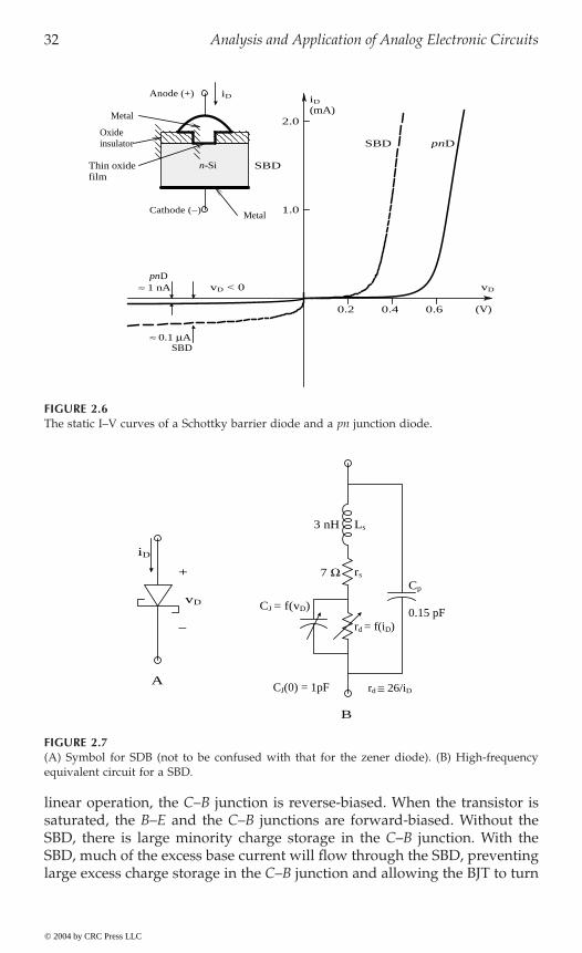
32 Analysis and Application of Analog Electronic Circuits
linear operation, the C–B junction is reverse-biased. When the transistor issaturated, the B–E and the C–B junctions are forward-biased. Without theSBD, there is large minority charge storage in the C–B junction. With theSBD, much of the excess base current will flow through the SBD, preventinglarge excess charge storage in the C–B junction and allowing the BJT to turn
FIGURE 2.6The static I–V curves of a Schottky barrier diode and a pn junction diode.
FIGURE 2.7(A) Symbol for SDB (not to be confused with that for the zener diode). (B) High-frequencyequivalent circuit for a SBD.
vD
iD
≈ 1 nA
(mA)
1.0
0.2 0.4 0.6 (V)
2.0
SBD pnD
pnD
SBD
vD < 0
≈ 0.1 µA
MetalCathode (−)
Oxideinsulator
Thin oxidefilm
Metal
n-Si SBD
Anode (+) iD
3 nH Ls
CJ = f(vD)0.15 pF
CJ(0) = 1pF rd ≅ 26/iD
Cp
7 Ω rs
rd = f(iD)
B
iD
+
−
vD
A
© 2004 by CRC Press LLC

Models for Semiconductor Devices Used in Analog Electronic Systems 33
off much more quickly (Yang, 1988). SBD thin film technology is also usedin the fabrication of certain MOS transistors (Nanavati, 1975).
2.3 Mid-Frequency Models for BJT Behavior
2.3.1 Introduction
Most BJTs found on ICs are silicon pnp or npn. (Other fabrication materials,such as gallium arsenide, exist but will not be treated here.) A heuristic view
are generally viewed as current-controlled current sources in their “linear”operating regions. As in the case of pn diodes, the large-signal, dc behaviorof these three terminal devices will first be examined. Figure 2.9(C) illustratestypical volt–ampere curves for a small-signal (as opposed to power) npn BJT.
For purposes of dc biasing and crude circuit calculations on paper, an npnBJT in its active region can be represented by the simple circuit shown in
resented by VBEQ on the order of 0.6 V. The dc collector current is approxi-mated by the current-controlled current source (CCCS) with gain bo. bo is thetransistor’s nominal (forward) dc current gain. Figure 2.10(B) illustrates thedc model for the transistor when it is saturated. Saturation occurs for iB >iC/bo, i.e., for high base currents. In saturation, the B–E and C–B junctionsare forward-biased, producing a VCEsat that can range from approximately0.2 to 0.8 V for high collector currents. The collector-emitter saturation curvecan be approximated by the simple Thevenin circuit shown: rcsat = ∂vCE/∂iC
at the operating point on the saturation curve; VCEsat is used to make themodel fit the published curves.
FIGURE 2.8Use of an SBD to make a Schottky transistor. The SBD prevents XS stored charge in the BJT’sC–B junction.
vCB+
+
vCE
−
−
iB+
vBE −
B
C
E
iE
iC
SBD
© 2004 by CRC Press LLC
of BJTs is shown by the “layer cake” models shown in Figure 2.9(B). BJTs
Figure 2.10(A). The voltage drop of the forward-biased B–E junction is rep-
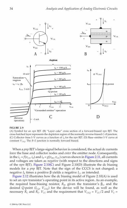
34 Analysis and Application of Analog Electronic Circuits
When a pnp BJT’s large-signal behavior is considered, the actual dc currentsleave the base and collector nodes and enter the emitter node. Consequently,in the iC = f(vCE, iB) and iB = g(vBE, vCE
and voltages are taken as negative (with respect to the directions and signs
models for a pnp BJT. Note that the sign of the CCCS is not changed; anegative IB times a positive b yields a negative IC, as intended.
to set an npn transistor’s operating point in its active region. As an example,the required base-biasing resistor, RB, given the transistor’s bo, and thedesired Q-point (ICQ, VCEQ) for the device will be found, as well as thenecessary RC and RE. VCC and the requirement that VCEQ = VCC/2 and VE =
FIGURE 2.9(A) Symbol for an npn BJT. (B) “Layer cake” cross section of a forward-biased npn BJT. Thecross-hatched layer represents the depletion region of the normally reverse-biased C–B junction.(C) Collector–base I–V curves as a function of iB for the npn BJT. (D) Base–emitter I–V curve atconstant VCEQ. The B–E junction is normally forward biased.
n
n
pIB
IB
VBEVBE
VCE
VCB
VCB
+
IE
+
IE
IC+
IC+ +
+
VCE
−
−
−
−
−−
5 mA
−5 mA
“Grounded emitter” operation
B
1 3VBEQ
IBQ
10 mA @ VCEQ
0
C D
Q point
A
ICQ
VCEQ
Q point
Saturationregion
iB > iC /βF
iC
vCE
iB = 0
(Reverseoperation)
iB = 20 µA
iB = 40 µA
iB = 60 µA
iB = 80 µA
iB = 100 µA
Active
iB
region
0 vBE
© 2004 by CRC Press LLC
) curves shown in Figure 2.11, all currents
of the npn BJT). Figure 2.10(C) and Figure 2.10(D) illustrate the dc biasing
Figure 2.12 illustrates how the dc biasing model of Figure 2.10(A) is used
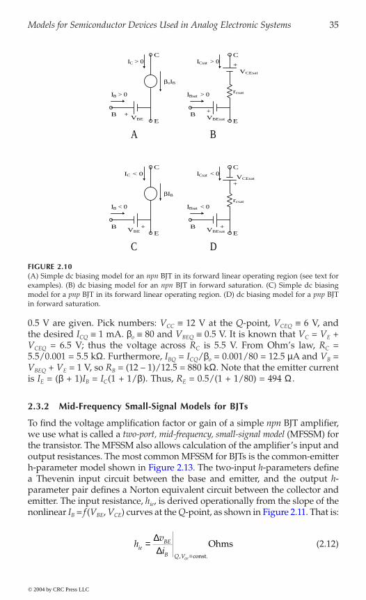
Models for Semiconductor Devices Used in Analog Electronic Systems 35
0.5 V are given. Pick numbers: VCC ∫ 12 V at the Q-point, VCEQ ∫ 6 V, andthe desired ICQ ∫ 1 mA. bo ∫ 80 and VBEQ ∫ 0.5 V. It is known that VC = VE +VCEQ = 6.5 V; thus the voltage across RC is 5.5 V. From Ohm’s law, RC =5.5/0.001 = 5.5 kW. Furthermore, IBQ = ICQ/bo = 0.001/80 = 12.5 mA and VB =VBEQ + VE = 1 V, so RB = (12 – 1)/12.5 = 880 kW. Note that the emitter currentis IE = (b + 1)IB = IC(1 + 1/b). Thus, RE = 0.5/(1 + 1/80) = 494 W .
2.3.2 Mid-Frequency Small-Signal Models for BJTs
To find the voltage amplification factor or gain of a simple npn BJT amplifier,we use what is called a two-port, mid-frequency, small-signal model (MFSSM) forthe transistor. The MFSSM also allows calculation of the amplifier’s input andoutput resistances. The most common MFSSM for BJTs is the common-emitter
a Thevenin input circuit between the base and emitter, and the output h-parameter pair defines a Norton equivalent circuit between the collector andemitter. The input resistance, hie, is derived operationally from the slope of thenonlinear IB = f (VBE, VCE
(2.12)
FIGURE 2.10(A) Simple dc biasing model for an npn BJT in its forward linear operating region (see text forexamples). (B) dc biasing model for an npn BJT in forward saturation. (C) Simple dc biasingmodel for a pnp BJT in its forward linear operating region. (D) dc biasing model for a pnp BJTin forward saturation.
+VBE
+VBEsat
rcsat
VCEsat
+
B B
βoIB
E E
C C
B
IB < 0
βIB
C
IC > 0
VBEB
E+
VBEsat E
+VCEsat
C
+ B
rcsat
D
IC < 0
IBsat < 0
C
ICsat < 0
A
ICsat > 0
IB > 0 IBsat > 0
hviieBE
B Q Vce
==
DD
, const.
Ohms
© 2004 by CRC Press LLC
h-parameter model shown in Figure 2.13. The two-input h-parameters define
) curves at the Q-point, as shown in Figure 2.11. That is:

36 Analysis and Application of Analog Electronic Circuits
FIGURE 2.11Top: a large-scale plot of a typical BJT’s iC vs. vCE curves. The Q point is the transistor’s quiescentoperating point. The small-signal conductance looking into the collector–emitter nodes is ap-proximated by go = DiC/DvCE siemens. The small-signal collector current gain is b = DiC/DiB.Bottom: the iB vs. vBE curve at the Q point. The small-signal resistance looking into the BJT’sbase is rb = DvBE/DiB ohms.
vCE
iB = 0
Q point∆vCE
∆ iC
iC
∆ iB
iB = 30 µA
iB =40 µA
iB = 20 µA
iB =50 µA
iB = IBQ
00
iB
vBE
∆ iB
ICQ
∆ iC
VCEQ
∆ vBE
VBEQ0
0
IBQ
Q point
@ VCEQ
iC @saturation
© 2004 by CRC Press LLC

Models for Semiconductor Devices Used in Analog Electronic Systems 37
FIGURE 2.12Model for dc biasing of an npn BJT with collector, base, and emitter resistors. See text for analysis.
FIGURE 2.13Top: an npn BJT viewed as a two-port circuit. Bottom: the linear, common-emitter, two-port,small-signal, h-parameter model for the BJT operating around some Q in its linear region. Notethat the input circuit is a Thevenin model and the output is a Norton model.
βoIB
VBE+
E
IB
C
VE
VC
IE
VB
RB
RC
VCC
RE
hrevcevbe hfe ib hoe vce
hie icib
B
B C
C
EE
E E
++ +
− − −
© 2004 by CRC Press LLC

38 Analysis and Application of Analog Electronic Circuits
hre is the gain of a voltage-controlled voltage source (VCVS), which modelshow the base voltage is modulated by changes in vCE. In other terms, hre isthe open-circuit reverse transfer voltage gain.
(2.13)
For most pencil-and-paper transistor gain calculations using the C–E SMF-SSM, hre is set to zero because it (1) has a second-order contribution tocalculations and (2) simplifies calculations. For the collector–base Nortonmodel, hoe is the output conductance that results from the iC = f (vCE, iB) curves
oe is given by:
(2.14)
Finally, the forward, current-controlled current source gain, hfe, is found:
(2.15)
hfe is also called the transistor’s b.One question that invariably arises concerns the MFSSM to be used when
a grounded emitter pnp transistor is considered. The answer is simple: thesame model as for an npn BJT. Whether a BJT is npn or pnp affects the dcbiasing of the transistors, not their gains and small-signal input and outputimpedances. The quiescent operating point of pnp and npn transistors affectsthe numerical values of the C–E h-parameters. For example, hre can be approx-imated by:
hre = rx + rp ohms (2.16)
where rx = the base spreading resistance, a fixed resistor with a range of 15 to150 W, and rp = the dynamic, SS resistance of the forward-biased base–emitterjunction.
The value of rp can be estimated from the basic diode equation for the B–Ejunction:
IB = Ibs exp(VBEQ/hVT) amps (2.17)
The resistance, rp, is given by:
(2.18)
hvvre
BE
CE Q iB
==
DD
, const.
hi
voeC
CE Q iB
==
DD
, const.
siemens
hiifeC
B Q Vce
==
DD
, const.
rg i v
VI
V h
IB BE
T
BQ
T fe
CQp
p
h h= =
∂ ∂= =1 1
ohms
© 2004 by CRC Press LLC
having a finite upward slope. Figure 2.11 shows that h
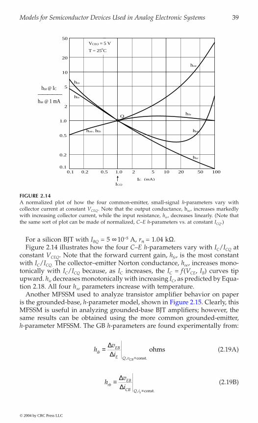
Models for Semiconductor Devices Used in Analog Electronic Systems 39
For a silicon BJT with IBQ = 5 ¥ 10-5 A, rp = 1.04 kW.Figure 2.14 illustrates how the four C–E h-parameters vary with IC/ICQ at
constant VCEQ. Note that the forward current gain, hfe, is the most constantwith IC/ICQ. The collector–emitter Norton conductance, hoe, increases mono-tonically with IC/ICQ because, as IC increases, the IC = f (VCE, IB) curves tipupward. hie decreases monotonically with increasing IC, as predicted by Equa-tion 2.18. All four hxe parameters increase with temperature.
Another MFSSM used to analyze transistor amplifier behavior on paper
MFSSM is useful in analyzing grounded-base BJT amplifiers; however, thesame results can be obtained using the more common grounded-emitter,h-parameter MFSSM. The GB h-parameters are found experimentally from:
(2.19A)
(2.19B)
FIGURE 2.14A normalized plot of how the four common-emitter, small-signal h-parameters vary withcollector current at constant VCEQ. Note that the output conductance, hoe, increases markedlywith increasing collector current, while the input resistance, hie, decreases linearly. (Note thatthe same sort of plot can be made of normalized, C–E h-parameters vs. at constant ICQ.)
0.1 1.0 10 1000.2 0.5 2 5 20 500.1
2
10
5hxe @ IC
hxe @ 1 mA
20
50
Qhfe
hoe
hie
IC (mA)
hie
hre
0.2
hre
VCEQ = 5 V
T = 25oC
ICQ
1.0
0.5hoe, hfe
hviibEB
E Q vCB
==
DD
, const.
ohms
hvirb
EB
CB Q ie
==
DD
, const.
© 2004 by CRC Press LLC
is the grounded-base, h-parameter model, shown in Figure 2.15. Clearly, this
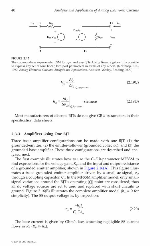
40 Analysis and Application of Analog Electronic Circuits
(2.19C)
(2.19D)
Most manufacturers of discrete BJTs do not give GB h-parameters in theirspecification data sheets.
2.3.3 Amplifiers Using One BJT
Three basic amplifier configurations can be made with one BJT: (1) thegrounded-emitter; (2) the emitter-follower (grounded collector); and (3) thegrounded-base amplifier. These three configurations are described and ana-lyzed next.
The first example illustrates how to use the C–E h-parameter MFSSM tofind expressions for the voltage gain, KV, and the input and output resistance
trates a basic grounded emitter amplifier driven by a small ac signal, vs,through a coupling capacitor, Cc. In the MFSSM amplifier model, only small-signal variations around the BJT’s operating (Q) point are considered; thusall dc voltage sources are set to zero and replaced with short circuits toground. Figure 2.16(B) illustrates the complete amplifier model (hre = 0 forsimplicity). The SS output voltage is, by inspection:
(2.20)
The base current is given by Ohm’s law, assuming negligible SS currentflows in RB (RB hie).
FIGURE 2.15The common-base h-parameter SSM for npn and pnp BJTs. Using linear algebra, it is possibleto express any set of four linear, two-port parameters in terms of any others. (Northrop, R.B.,1990, Analog Electronic Circuits: Analysis and Applications, Addison–Wesley, Reading, MA.)
ie hibE
B B
C ic
hrbvcb
+
−
hfbie
hob vcb
+
−
hiifbC
E Q vCB
==
DD
, const.
hi
vobC
CB Q iE
==
DD
, const.
siemens
vh i
G hofe b
c oe
=-
+
© 2004 by CRC Press LLC
of a grounded emitter amplifier, shown in Figure 2.16(A). This figure illus-
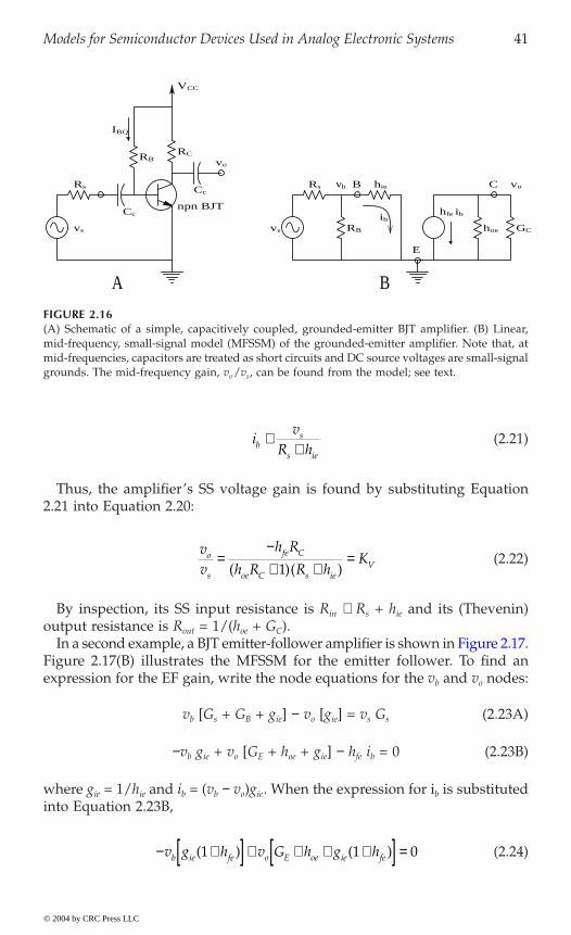
Models for Semiconductor Devices Used in Analog Electronic Systems 41
(2.21)
Thus, the amplifier’s SS voltage gain is found by substituting Equation2.21 into Equation 2.20:
(2.22)
By inspection, its SS input resistance is Rin @ Rs + hie and its (Thevenin)output resistance is Rout = 1/(hoe + GC).
Figure 2.17(B) illustrates the MFSSM for the emitter follower. To find anexpression for the EF gain, write the node equations for the vb and vo nodes:
vb [Gs + GB + gie] - vo [gie] = vs Gs (2.23A)
-vb gie + vo [GE + hoe + gie] - hfe ib = 0 (2.23B)
where gie = 1/hie and ib = (vb - vo)gie. When the expression for ib is substitutedinto Equation 2.23B,
(2.24)
FIGURE 2.16(A) Schematic of a simple, capacitively coupled, grounded-emitter BJT amplifier. (B) Linear,mid-frequency, small-signal model (MFSSM) of the grounded-emitter amplifier. Note that, atmid-frequencies, capacitors are treated as short circuits and DC source voltages are small-signalgrounds. The mid-frequency gain, vo /vs, can be found from the model; see text.
RB
ib
RB
hoe GC
RsCc
RC
VCC
vs
Cc
vo
npn BJT
IBQ
B
E
hie vo
hfe ib
C
B
vbRs
vs
A
iv
R hbs
s ie
@+
vv
h R
h R R hKo
s
fe C
oe C s ieV=
-+ +
=( )( )1
- +[ ] + + + +[ ] =v g h v G h g hb ie fe o E oe ie fe( ) ( )1 1 0
© 2004 by CRC Press LLC
In a second example, a BJT emitter-follower amplifier is shown in Figure 2.17.

42 Analysis and Application of Analog Electronic Circuits
Now Equation 2.23A and Equation 2.24 are solved using Cramer’s rule,yielding the voltage gain:
(2.25)
This rather unwieldy expression can be simplified using the a priori knowl-edge that, usually, GE hoe and Gs GB. Equation 2.25 is multiplied top andbottom by hie RE Rs. After some algebra, the simplified EF gain is found to be:
(2.26)
Note that Kv for the EF is positive (noninverting) and slightly less than 1.What then is the point of an amplifier with no gain? The answer lies in theEF’s high input impedance and low output impedance. The EF is used tobuffer sources and drive coaxial cables and transmission lines with lowcharacteristic impedances. It is easy to show that the EF’s input impedanceat the vb node is simply RB in parallel with [hie + RE (1 + hfe)] (hoe is neglected).The Thevenin output impedance can be found for the linear MFSSM bytaking the ratio of the open circuit voltage (OCV) to its short-circuit current(SCC). The OCV is simply vs KV:
(2.27)
FIGURE 2.17(A) Schematic of a simple, capacitively coupled, emitter-follower amplifier. (B) MFSSM of theEF amplifier.
(hfe + 1)ibRE
Evo
vs
Rs hie
RB hoe
ib
Cnpn BJT vb
RE
Cc vo
RB
vs
RsCc
B hfe ib
VCC
A B
vv
G g h
G G G h g h g G hKo
s
s ie fe
s B E oe ie fe ie E oe
V=+( )
+( ) + + +( )[ ] + +( )=
1
1
KR h
R h h RV
E fe
E fe ie s
@+( )
+( ) + +
1
1
Vv R h
R h h ROC
s E fe
E fe ie s
@+( )
+( ) + +
1
1
© 2004 by CRC Press LLC
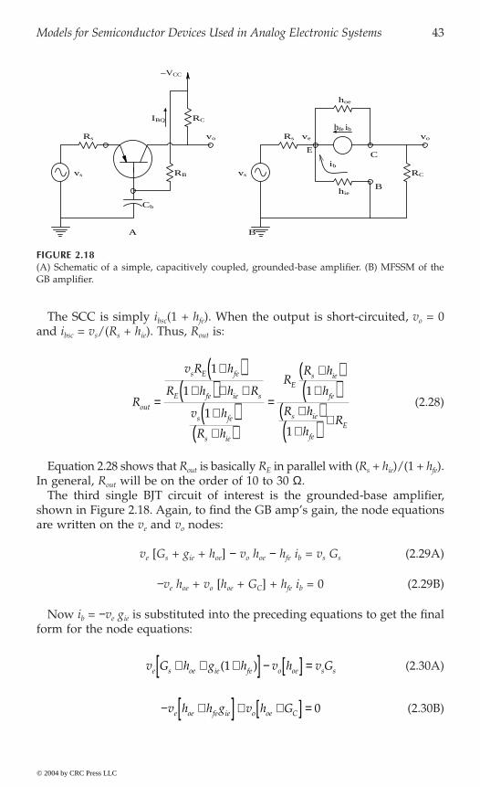
Models for Semiconductor Devices Used in Analog Electronic Systems 43
The SCC is simply ibsc(1 + hfe). When the output is short-circuited, vo = 0and ibsc = vs/(Rs + hie). Thus, Rout is:
(2.28)
Equation 2.28 shows that Rout is basically RE in parallel with (Rs + hie)/(1 + hfe).In general, Rout will be on the order of 10 to 30 W.
The third single BJT circuit of interest is the grounded-base amplifier,shown in Figure 2.18. Again, to find the GB amp’s gain, the node equationsare written on the ve and vo nodes:
ve [Gs + gie + hoe] - vo hoe - hfe ib = vs Gs (2.29A)
-ve hoe + vo [hoe + GC] + hfe ib = 0 (2.29B)
Now ib = -ve gie is substituted into the preceding equations to get the finalform for the node equations:
(2.30A)
(2.30B)
FIGURE 2.18(A) Schematic of a simple, capacitively coupled, grounded-base amplifier. (B) MFSSM of theGB amplifier.
ve vo
vsvs
Rs Rs
hie
hoe
hfe ib
ib
B
CE
RC
RCRB
Cb
vo
IBQ
−VCC
A B
R
v R h
R h h R
v h
R h
RR h
h
R h
hR
out
s E fe
E fe ie s
s fe
s ie
Es ie
fe
s ie
fe
E
=
+( )+( ) + +
+( )+( )
=
+( )+( )
+( )+( ) +
1
1
1
1
1
v G h g h v h v Ge s oe ie fe o oe s s+ + +[ ] - [ ] =( )1
- +[ ] + +[ ] =v h h g v h Ge oe fe ie o oe C 0
© 2004 by CRC Press LLC
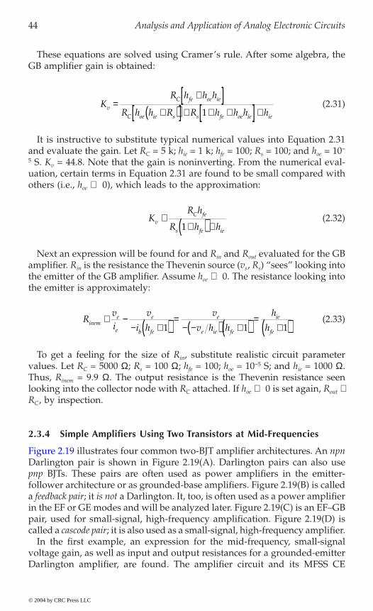
44 Analysis and Application of Analog Electronic Circuits
These equations are solved using Cramer’s rule. After some algebra, theGB amplifier gain is obtained:
(2.31)
It is instructive to substitute typical numerical values into Equation 2.31and evaluate the gain. Let RC = 5 k; hie = 1 k; hfe = 100; Rs = 100; and hoe = 10-
5 S. Kv = 44.8. Note that the gain is noninverting. From the numerical eval-uation, certain terms in Equation 2.31 are found to be small compared withothers (i.e., hoe Æ 0), which leads to the approximation:
(2.32)
Next an expression will be found for and Rin and Rout evaluated for the GBamplifier. Rin is the resistance the Thevenin source (vs, Rs) “sees” looking intothe emitter of the GB amplifier. Assume hoe Æ 0. The resistance looking intothe emitter is approximately:
(2.33)
To get a feeling for the size of Rin, substitute realistic circuit parametervalues. Let RC = 5000 W; Rs = 100 W; hfe = 100; hoe = 10-5 S; and hie = 1000 W.Thus, Rinem = 9.9 W. The output resistance is the Thevenin resistance seenlooking into the collector node with RC attached. If hoe Æ 0 is set again, Rout @RC, by inspection.
2.3.4 Simple Amplifiers Using Two Transistors at Mid-Frequencies
Darlington pair is shown in Figure 2.19(A). Darlington pairs can also usepnp BJTs. These pairs are often used as power amplifiers in the emitter-follower architecture or as grounded-base amplifiers. Figure 2.19(B) is calleda feedback pair; it is not a Darlington. It, too, is often used as a power amplifierin the EF or GE modes and will be analyzed later. Figure 2.19(C) is an EF–GBpair, used for small-signal, high-frequency amplification. Figure 2.19(D) iscalled a cascode pair; it is also used as a small-signal, high-frequency amplifier.
In the first example, an expression for the mid-frequency, small-signalvoltage gain, as well as input and output resistances for a grounded-emitterDarlington amplifier, are found. The amplifier circuit and its MFSS CE
KR h h h
R h h R R h h h hv
C fe oe ie
C oe ie s s fe oe ie ie
=+[ ]
+( )[ ] + + +[ ] +1
KR h
R h hv
C fe
s fe ie
@+( ) +1
Rvi
v
i h
v
v h h
h
hinem
e
e
e
b fe
e
e ie fe
ie
fe
@ -- +( ) =
- -( ) +( ) =+( )1 1 1
© 2004 by CRC Press LLC
Figure 2.19 illustrates four common two-BJT amplifier architectures. An npn
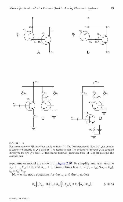
Models for Semiconductor Devices Used in Analog Electronic Systems 45
RB Æ •, hoe1 Æ 0, and hoe2 b1 = (vs – vb2)/(Rs + hie1),ib2 = vb2/hie2.
Now write node equations for the vb2 and the vo nodes:
(2.34A)
FIGURE 2.19Four common two-BJT amplifier configurations: (A) The Darlington pair. Note that Q1’s emitteris connected directly to Q2’s base. (B) The feedback pair. The collector of the pnp Q1 is coupleddirectly to the npn Q2’s base. (C) The emitter-follower–grounded-base (EF–GB) BJT pair. (D) Thecascode pair.
A
C
Q1
Q1
Q2
Q1 Q2
Q2 Q2
Q1
C1
C1
C2
C2
E2 E2
B2 B2E1
E1
B1 B1
RE
RE
RC RCRB RB RB RB
VCC VCC
vo vo
vs
vs
B
D
v h R h h i v R hb ie s ie fe b s s ie2 2 1 1 1 11 1+ +( )[ ] - = +( )
© 2004 by CRC Press LLC
Æ 0. From Ohm’s law, ih-parameter model are shown in Figure 2.20. To simplify analysis, assume
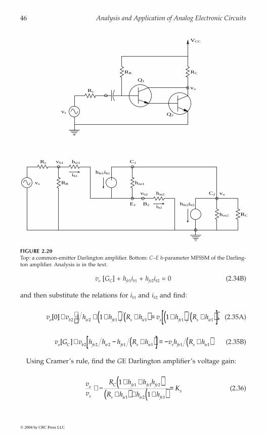
46 Analysis and Application of Analog Electronic Circuits
vo [GC] + hfe1ib1 + hfe2ib2 = 0 (2.34B)
and then substitute the relations for ib1 and ib2 and find:
(2.35A)
(2.35B)
Using Cramer’s rule, find the GE Darlington amplifier’s voltage gain:
(2.36)
FIGURE 2.20Top: a common-emitter Darlington amplifier. Bottom: C–E h-parameter MFSSM of the Darling-ton amplifier. Analysis is in the text.
RB
RC
RChoe2
hie2
hie1
hoe1
ib1
hfe2ib2B2E1 ib2
Rs
vs
vovb2
vb1
vs
Rsvo
VCC
C1
C2
hfe1ib1
Q1
Q2
RB
v v h h R h v h R ho b ie fe s ie s fe s ie[ ]0 1 1 12 2 1 1 1 1+ + +( ) +( ) = +( ) +( )[ ]ÈÎÍ
˘˚
v G v h h h R h v h R ho C b fe ie fe s ie s fe s ie[ ] + - +( )[ ] = - +( )2 2 2 1 1 1 1
vv
R h h h
R h h hKo
s
C fe fe fe
s ie ie fe
v@ -+ +( )
+( ) + +( ) =1
1
1 1 2
1 2 1
© 2004 by CRC Press LLC
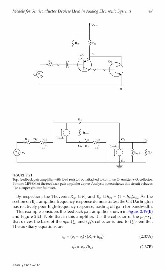
Models for Semiconductor Devices Used in Analog Electronic Systems 47
By inspection, the Thevenin Rout @ RC and Rin @ hie1 + (1 + hfe1)hie2. As thesection on BJT amplifier frequency response demonstrates, the GE Darlingtonhas relatively poor high-frequency response, trading off gain for bandwidth.
and Figure 2.21. Note that in this amplifier, it is the collector of the pnp Q1
that drives the base of the npn Q2, and Q2’s collector is tied to Q1’s emitter.The auxiliary equations are:
ib1 = (vs – vo)/(Rs + hie1) (2.37A)
ib2 = vb2/hie2 (2.37B)
FIGURE 2.21Top: feedback pair amplifier with load resistor, RC, attached to common Q1 emitter + Q2 collector.Bottom: MFSSM of the feedback pair amplifier above. Analysis in text shows this circuit behaveslike a super emitter follower.
E1
B1hfe1ib1
hoe1
C1 B2ib1 ib2hfe2ib2
C2
E2
hoe2 GC
vo
vs
Rs hie1 hie2vb2
RB RC
VCC
vo
vs
Rs
Q1
Q2
© 2004 by CRC Press LLC
This example considers the feedback pair amplifier shown in Figure 2.19(B)
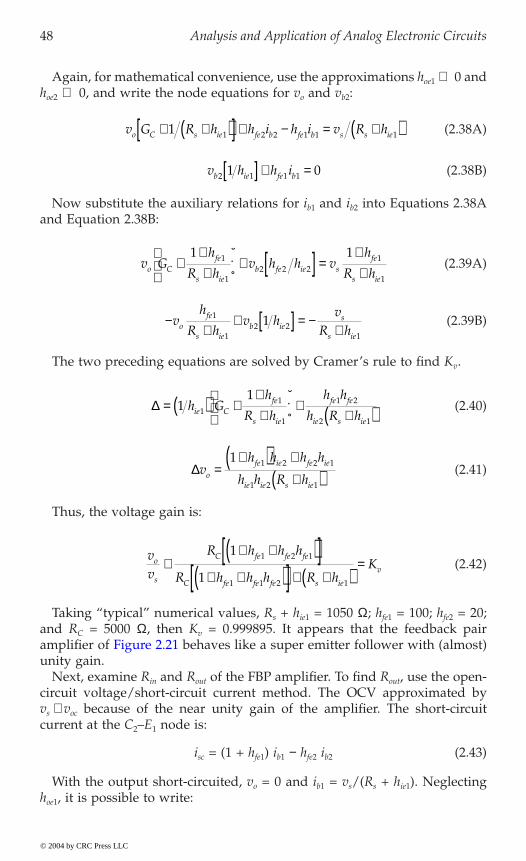
48 Analysis and Application of Analog Electronic Circuits
Again, for mathematical convenience, use the approximations hoe1 Æ 0 andhoe2 Æ 0, and write the node equations for vo and vb2:
(2.38A)
(2.38B)
Now substitute the auxiliary relations for ib1 and ib2 into Equations 2.38Aand Equation 2.38B:
(2.39A)
(2.39B)
The two preceding equations are solved by Cramer’s rule to find Kv.
(2.40)
(2.41)
Thus, the voltage gain is:
(2.42)
Taking “typical” numerical values, Rs + hie1 = 1050 W; hfe1 = 100; hfe2 = 20;and RC = 5000 W, then Kv = 0.999895. It appears that the feedback pair
unity gain.Next, examine Rin and Rout of the FBP amplifier. To find Rout, use the open-
circuit voltage/short-circuit current method. The OCV approximated byvs @ voc because of the near unity gain of the amplifier. The short-circuitcurrent at the C2–E1 node is:
isc = (1 + hfe1) ib1 - hfe2 ib2 (2.43)
With the output short-circuited, vo = 0 and ib1 = vs/(Rs + hie1). Neglectinghoe1, it is possible to write:
v G R h h i h i v R ho C s ie fe b fe b s s ie+ +( )[ ] + - = +( )1 1 2 2 1 1 1
v h h ib ie fe b2 1 1 11 0[ ] + =
v Gh
R hv h h v
h
R ho Cfe
s ieb fe ie s
fe
s ie
++
+È
ÎÍ
˘
˚˙ + [ ] =
++
1 11
12 2 2
1
1
-+
+ [ ] = -+
vh
R hv h
vR ho
fe
s ieb ie
s
s ie
1
12 2
1
1
D = ( ) ++
+È
ÎÍ
˘
˚˙ +
+( )11
11
1
1 2
2 1
h Gh
R h
h h
h R hie Cfe
s ie
fe fe
ie s ie
Dvh h h h
h h R hofe ie fe ie
ie ie s ie
=+( ) +
+( )1 1 2 2 1
1 2 1
vv
R h h h
R h h h R hKo
s
C fe fe fe
C fe fe fe s ie
v@+ +( )[ ]
+ +( )[ ] + +( )=
1
1
1 2 1
1 1 2 1
© 2004 by CRC Press LLC
amplifier of Figure 2.21 behaves like a super emitter follower with (almost)
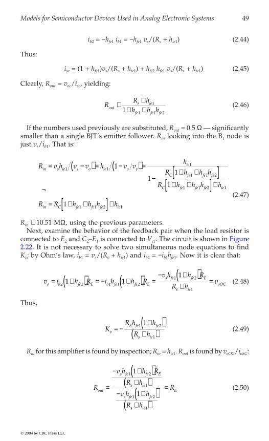
Models for Semiconductor Devices Used in Analog Electronic Systems 49
ib2 = -hfe1 ib1 = -hfe1 vs/(Rs + hie1) (2.44)
Thus:
isc = (1 + hfe1)vs/(Rs + hie1) + hfe2 hfe1 vs/(Rs + hie1) (2.45)
Clearly, Rout = voc/isc, yielding:
(2.46)
If the numbers used previously are substituted, Rout = 0.5 W — significantlysmaller than a single BJT’s emitter follower. Rin looking into the B1 node isjust vs/ib1. That is:
(2.47)
Rin @ 10.51 MW, using the previous parameters.Next, examine the behavior of the feedback pair when the load resistor is
connected to E2 and C2–E1 is connected to Vcc
Kv; by Ohm’s law, ib1 = vs/(Rs + hie1) and ib2 = -ib1hfe1. Now it is clear that:
(2.48)
Thus,
(2.49)
Rin for this amplifier is found by inspection; Rin = hie1. Rout is found by voOC/ioSC:
(2.50)
RR hh h hout
s ie
fe fe fe
@+
+ +1
1 1 21
R v h v v h v vh
R h h h
R h h h h
R R h h h h
in s ie s o ie o sie
C fe fe fe
C fe fe fe ie
in C fe fe fe ie
= -( ) = -( ) =
-+ +[ ]
+ +[ ] +Ø
= + +[ ] +
1 11
1 1 2
1 1 2 1
1 1 2 1
1
11
1
1
v i h R i h h Rv h h R
R hvo b fe E b fe fe E
s fe fe E
s ieoOC= +( ) = - +( ) =
- +( )+
=2 2 1 1 21 2
1
1 11
KR h h
R hvE fe fe
s ie
= -+( )
+( )1 2
1
1
R
v h h R
R h
v h h
R h
Rout
s fe fe E
s ie
s fe fe
s ie
E=
- +( )+( )
- +( )+( )
=
1 2
1
1 2
1
1
1
© 2004 by CRC Press LLC
. The circuit is shown in Figure2.22. It is not necessary to solve two simultaneous node equations to find
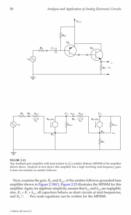
50 Analysis and Application of Analog Electronic Circuits
Next, examine the gain, Rin and Rout, of the emitter-follower-grounded base
amplifier. Again, for algebraic simplicity, assume that hoe1 and hoe2 are negligible;also, R1 = Rs + hie1, all capacitors behave as short circuits at mid-frequencies,and RB Æ •. Two node equations can be written for the MFSSM:
FIGURE 2.22Top: feedback pair amplifier with load resistor in Q2’s emitter. Bottom: MFSSM of the amplifiershown above. Analysis in text shows this amplifier has a high inverting mid-frequency gain;it does not emulate an emitter follower.
hfe2ib2
E2
vs
Rs
Q1
Q2
hoe2
vo
Rs hie1B1
hfe1ib1
E1
C1
hoe1
hie2vb2 C2
RE
ib2ib1B2
RB
VCC
Cc
vs
RE vo
+
© 2004 by CRC Press LLC
amplifier shown in Figure 2.19(C). Figure 2.23 illustrates the MFSSM for this
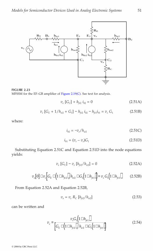
Models for Semiconductor Devices Used in Analog Electronic Systems 51
vo [GC] + hfe2 ib2 = 0 (2.51A)
ve [GE + 1/hie2 + G1] - hfe2 ib2 - hfe1ib1 = vs G1 (2.51B)
where:
ib2 = -ve/hie2 (2.51C)
ib1 = (vs – ve)G1 (2.51D)
Substituting Equation 2.51C and Equation 2.51D into the node equationsyields:
vo [GC] - ve [hfe2/hie2] = 0 (2.52A)
(2.52B)
From Equation 2.52A and Equation 2.52B,
vo = ve RC [hfe2/hie2] (2.53)
can be written and
(2.54)
FIGURE 2.23
Rs hie1
hfe1ib1
ib1
B1
hoe1
RE
E1 E2
C1 C2vo
hie2
RC
hfe2 ib2
hoe2
B2
ve
vs
v v G h h G h v G ho e E fe ie fe s fe0 1 1 12 2 1 1 1 1[ ] + + +( ) + +( )[ ] = +( )
vv G h
G h h G he
s fe
E fe ie fe
=+( )
+ +( ) + +( )[ ]1 1
2 2 1 1
1
1 1
© 2004 by CRC Press LLC
MFSSM for the EF–GB amplifier of Figure 2.19(C). See text for analysis.
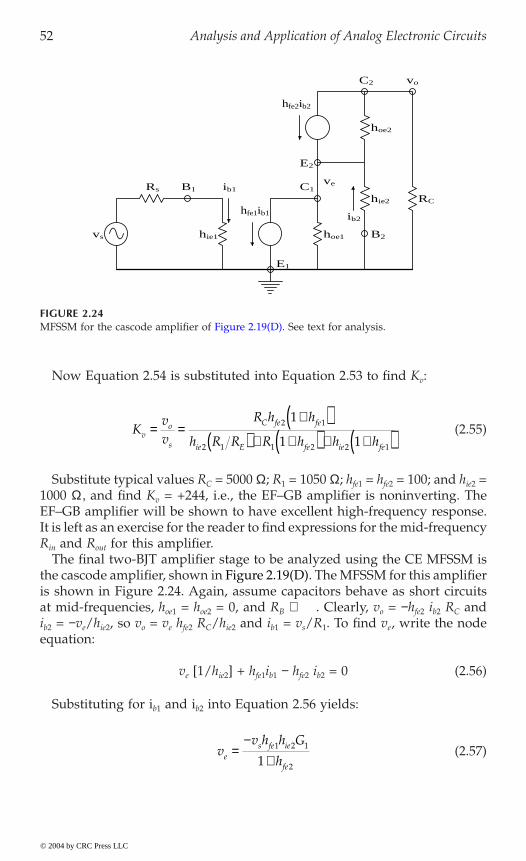
52 Analysis and Application of Analog Electronic Circuits
Now Equation 2.54 is substituted into Equation 2.53 to find Kv:
(2.55)
Substitute typical values RC = 5000 W; R1 = 1050 W; hfe1 = hfe2 = 100; and hie2 =1000 W, and find Kv = +244, i.e., the EF–GB amplifier is noninverting. TheEF–GB amplifier will be shown to have excellent high-frequency response.It is left as an exercise for the reader to find expressions for the mid-frequencyRin and Rout for this amplifier.
at mid-frequencies, hoe1 = hoe2 = 0, and RB Æ •. Clearly, vo = -hfe2 ib2 RC andib2 = -ve/hie2, so vo = ve hfe2 RC/hie2 and ib1 = vs/R1. To find ve, write the nodeequation:
ve [1/hie2] + hfe1ib1 - hfe2 ib2 = 0 (2.56)
Substituting for ib1 and ib2 into Equation 2.56 yields:
(2.57)
FIGURE 2.24
hie1
hfe1ib1
ib1
hoe1
hoe2
ib2
hie2 RC
hfe2ib2
E1
B1 C1
E2
C2
B2
vo
Rsve
vs
Kvv
R h h
h R R R h h hv
o
s
C fe fe
ie E fe ie fe
= =+( )
( ) + +( ) + +( )2 1
2 1 1 2 2 1
1
1 1
vv h h G
hes fe ie
fe
=-
+1 2 1
21
© 2004 by CRC Press LLC
MFSSM for the cascode amplifier of Figure 2.19(D). See text for analysis.
The final two-BJT amplifier stage to be analyzed using the CE MFSSM is
is shown in Figure 2.24. Again, assume capacitors behave as short circuitsthe cascode amplifier, shown in Figure 2.19(D). The MFSSM for this amplifier

Models for Semiconductor Devices Used in Analog Electronic Systems 53
Equation 2.57 is substituted into the preceding equation for vo to find Kv:
(2.58)
By inspection, Rin = R1, Rout @ RC. Like the EF–GB amplifier, the cascodeamplifier has a high-frequency bandwidth. It also can be described as aGE–GB amplifier.
2.3.5 The Use of Transistor Dynamic Loads To Improve Amplifier Performance
In many analog IC designs, including those with differential amplifiers,transistors and small transistor circuits are used to create small-signal,dynamic high impedances that, when used in amplifiers to replace conven-tional resistors, increase amplifier gain or differential amplifier common-mode
sources or sinks with high, small-signal, Norton resistances. For example, if2 mA dc flows through a potential difference of 5 V in an electronic circuit,a 2.5-k resistor is needed. If a dynamic current source is used, the equivalentsmall-signal (Norton) resistance can range from 100 k to 10 M, dependingon the circuit. A good way to view such dynamic resistances is to treat thecircuit as a dc current source in parallel with a Norton resistance of 100 k to10 M.
The most basic dynamic resistance is realized by looking into the collector
looking into the collector. Note that the base is bypassed to ground at signalfrequencies. Clearly, from Ohm’s law, Rincol = vt/it. (vt is a small-signal testsource.)
Begin analysis by finding an expression for ve = f (vt). Writing the nodeequation:
(2.59A)
(2.59B)
Ø
(2.59C)
Kvv
h R h
R h
h R
Rvo
s
fe C fe
fe
fe C= =-
+( ) ª-1 2
1 2
1
11
v h G h i v he ie E oe b t oe1( ) + +[ ] - =b
i v hb e ie= -
v h G h v he ie e oe t oe1 1( ) +( ) + +[ ] =b
© 2004 by CRC Press LLC
rejection ratio. Figure 2.25 illustrates four BJT circuits that act as dc current
of a BJT with an emitter resistance that is not bypassed, as shown in Figure2.25(A). Figure 2.26 illustrates how the MFSSM is used to find the resistance
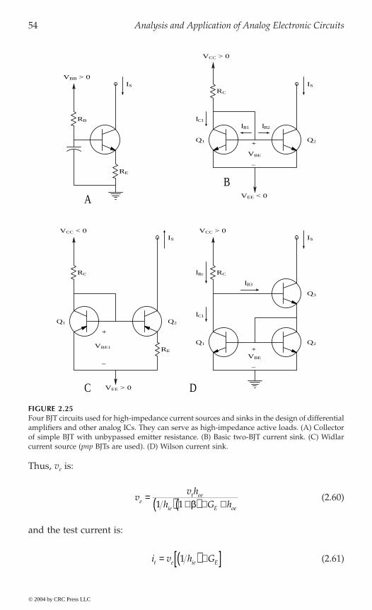
54 Analysis and Application of Analog Electronic Circuits
Thus, ve is:
(2.60)
and the test current is:
(2.61)
FIGURE 2.25Four BJT circuits used for high-impedance current sources and sinks in the design of differentialamplifiers and other analog ICs. They can serve as high-impedance active loads. (A) Collectorof simple BJT with unbypassed emitter resistance. (B) Basic two-BJT current sink. (C) Widlarcurrent source (pnp BJTs are used). (D) Wilson current sink.
RE
RC RC
RB
VBB > 0
VCC > 0
RC
VEE < 0
VCC < 0 VCC > 0
A
B
C D
Q1
Q1
Q1
Q2
Q2
Q2
RE
Q3
IB3
IRc
IC1
−
+
VBE
IB2IB1
IC1
IS IS
ISIS
VBE
+
VEE > 0
−
VBE1
+
−
vv h
h G het oe
ie E oe
= ( ) +( ) + +1 1 b
i v h Gt e ie E= ( ) +[ ]1
© 2004 by CRC Press LLC
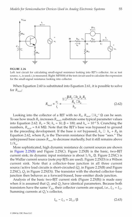
Models for Semiconductor Devices Used in Analog Electronic Systems 55
When Equation 2.60 is substituted into Equation 2.61, it is possible to solvefor Rincol:
(2.62)
Looking into the collector of a BJT with no RE, Rincol @ hoe-1 W can be seen.
To see how much RE increases Rincol, substitute some typical parameter valuesinto Equation 2.62: RE = 5k; hie = 1k; b = 100; and hoe = 10-5 S. Crunching thenumbers, Rincol = 8.4 MW. Note that the BJT’s base was bypassed to groundin the preceding development. If the base is not bypassed, hie Æ hie + RB inEquation 2.62, where RB is the Thevenin resistance that the base “sees.” Theunbypassed base causes Rincol to decrease markedly, but it still remains above1/hoe.
More sophisticated, high dynamic resistance dc current sources are shown
current sink; its dynamic input resistance is about 1/hoe W. Figure 2.25(C) isthe Widlar current source (note pnp BJTs are used). Figure 2.25(D) is a Wilsoncurrent sink. Note that a collector–base junction in all three currentsource/active load circuits is short-circuited (Q1 in Figure 2.25(B) and Figure2.25(C), Q2 in Figure 2.25(D)). The transistor with the shorted collector–basejunction then behaves as a forward-biased, base–emitter diode junction.
Analysis of the basic two-BJT current sink (Figure 2.25(B)) is made easywhen it is assumed that Q1 and Q2 have identical parameters. Because bothtransistors have the same VBE, their collector currents are equal, i.e., IC1 = IC2.Summing currents at Q1’s collector,
IRc - IC1 = 2IC1/b (2.63)
FIGURE 2.26Left: test circuit for calculating small-signal resistance looking into BJT’s collector. An ac testsource, vt, is used; it is measured. Right: MFSSM of the test circuit used to calculate the expressionfor the small-signal resistance looking into collector.
vt
+
it
vt
+
itvehie
ib
β ib
hoe
RB
Cb
RERE
B
E C
VBB
Rvi
R h h RR hhincol
t
t
E oe ie E
E ie
oe
= =+
++
1b
© 2004 by CRC Press LLC
in Figure 2.25(B) and Figure 2.25(C). Figure 2.25(B) is the basic, two-BJT
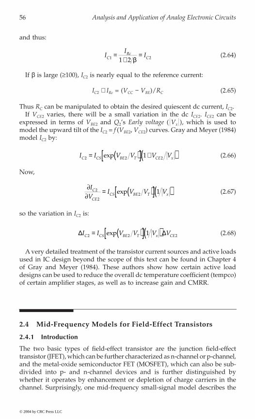
56 Analysis and Application of Analog Electronic Circuits
and thus:
(2.64)
If b is large (≥100), IC2 is nearly equal to the reference current:
IC2 @ IRc = (VCC - VBE)/RC (2.65)
Thus RC can be manipulated to obtain the desired quiescent dc current, IC2. If VCE2 varies, there will be a small variation in the dc ICE2. ICE2 can be
expressed in terms of VBE2 and Q2’s Early voltage ( Vx ), which is used tomodel the upward tilt of the IC2 = f (VBE2, VCE2) curves. Gray and Meyer (1984)model IC2 by:
(2.66)
Now,
(2.67)
so the variation in IC2 is:
(2.68)
A very detailed treatment of the transistor current sources and active loadsused in IC design beyond the scope of this text can be found in Chapter 4of Gray and Meyer (1984). These authors show how certain active loaddesigns can be used to reduce the overall dc temperature coefficient (tempco)of certain amplifier stages, as well as to increase gain and CMRR.
2.4 Mid-Frequency Models for Field-Effect Transistors
2.4.1 Introduction
The two basic types of field-effect transistor are the junction field-effecttransistor (JFET), which can be further characterized as n-channel or p-channel,and the metal-oxide semiconductor FET (MOSFET), which can also be sub-divided into p- and n-channel devices and is further distinguished bywhether it operates by enhancement or depletion of charge carriers in thechannel. Surprisingly, one mid-frequency small-signal model describes the
II
ICRc
C1 21 2=
+=
b
I I V V V VC CS BE T CE x2 2 21= ( )[ ] +( )exp
∂∂
= ( )[ ]( )IV
I V V VC
CECS BE T x
2
22 1exp
D DI I V V V VC CS BE T x CE2 2 21= ( )[ ]( )exp
© 2004 by CRC Press LLC

Models for Semiconductor Devices Used in Analog Electronic Systems 57
behavior of all types of FETs, although the dc biasing varies. MFSSMs forFETs use a voltage-controlled current source (transconductance) model inparallel with an output conductance to model the drain-to-source behavior.The following sections examine the behavior of JFETs and how they workas amplifiers.
2.4.2 JFETs at Mid-Frequencies
Figure 2.27 illustrates the symbols for n- and p-channel JFETs and thevolt–ampere curves for an n-channel JFET. Note that the gate-to-channel pnjunction is normally reverse-biased in a JFET; thus, the gate current is thereverse saturation current of this diode (Irs), which is on the order of nA. Inthe n-channel JFET, all the currents and voltages are positive as written, withvGS being negative. In the p-channel JFET, all the signs are reversed: iD andvDS are negative and vGS is positive. The operating region of the JFET’s (iD, vDS)curves is ohmic to the left of the IDB line and saturated to the right of the IDB line.
FIGURE 2.27Top: symbols for n- and p-channel JFETs. Bottom left: iD vs. vDS curves for an n-channel JFET.Area to left of IDB parabola has ohmic FET operation; area to right of IDB line has saturated(channel) operation. Bottom right: the iD vs. vGS curve for saturated operation [vDS > ΩvGS + VPΩ].The pinch-off voltage VP = -4 V in this example.
S
D D
vDS
S
vDS
+
G G
+
+ +
iD iD
−−
−−
vGS vGS
n-channel p-channel
vGS = −1 V
vGS = −2 V
vGS = −3 V
IDB = IDSS (VDS /VP)2
iD vGS = 0iD
00
vGS
−4 −3 −2 −142 6 8 10 12 14
vGS = VP = −4 V vDS
BVGD
IDSS IDSS
vDS > vGS + vP
© 2004 by CRC Press LLC

58 Analysis and Application of Analog Electronic Circuits
Just as there is a mathematical model for pn junction diode current, thereis also a mathematical approximation to JFET behavior in the saturationregion. This is:
(2.69)
In the ohmic region, ID is modeled by:
(2.70)
For VGS VP,
(2.71)
where IDSS is the drain current defined for VGS = 0 and VDS > VGS + VP . VP
is the pinch-off voltage, i.e., VP = VGS where ID Æ 0, given VDS > VGS + VP .In the ohmic region, the JFET behaves like a voltage-controlled conductance:
(2.72)
In the saturation region, n- and p-channel JFETs have the same MFSSM,shown in Figure 2.28. The transconductance of the VCCS is defined by:
(2.73)
By differentiating Equation 2.69, an algebraic expression is found for gm:
(2.74)
FIGURE 2.28Left: symbol for n-channel JFET. Center: Norton MFSSM for p- and n-channel JFETs. Right:Thevenin MFSSM for JFETs.
µvgsvgs
rd
vds
+
+
+
+vDS
−
−
−
G
G
S S S S S
D
id+ G D
gmvgs++
vgs gd vds
vGS −− − −
id
DiD
I I V V V V V V VD DSS GS P DS GS p GS P= -( ) > + <12 for and
I I V V V V V V V V VD DSS GS P DS P DS P DS GS p= +( )( ) - ( )[ ] < < +2 1 02
for
I I V V V VD DSS GS P DS P= +( )( )[ ]2 1
gi
vV I V V Vd
D
DSGS DSS GS P P= ∂
∂= + ( )( )[ ]2 1
gi
vQ Vm
D
DSGS= ∂
∂=, const.
gIV
V VmDSS
PGS P= -( )2
1
© 2004 by CRC Press LLC

Models for Semiconductor Devices Used in Analog Electronic Systems 59
Note from Equation 2.69 that can be written as:
(2.75)
Now Equation 2.75 can be substituted into Equation 2.74 to find:
(2.76)
Equation 2.76 gives an algebraic means of estimating a JFET’s gm in termsof its quiescent drain current (IDQ) and the manufacturer-specified parame-ters, IDSS and VP. gmo is the JFET’s (maximum) transconductance at VGS = 0and VDS > VGS + VP .
The MFSSM for a saturated-channel JFET is also characterized by an outputconductance in parallel with the VCCS. This small-signal conductance is duein part to the upward slope of the iD = f(vGS, vDS) curve family :
(2.77)
To model the upward slope of the iD = f(vGS, vDS) curve family, we choosea voltage Vx such that:
(2.78)
Note that the intercept voltage, Vx, is typically 25 to 50 V in magnitude.Vx is negative and VDS is positive for n-channel JFETs and Vx is positive andVDS is negative for p-channel JFETs. An algebraic expression for gd can befound by differentiating Equation 2.78.
(2.79)
An estimate of Vx can be found by extrapolating the iD = f(vGS, vDS) curvesin the saturation region back to the negative VSD
Thevenin model in which the series Thevenin resistance is just rd = 1/gd andthe open-circuit voltage is given by a VCVS, mvGS. (Note the sign of the VCVS;it is the same for n- and p-channel JFETs.
The voltage gain, m, is easily seen to be given by:
ID
I I V VD DSS GS P= -( )1
gIV
I
Ig
I
IV V Vm
DSS
P
DQ
DSSmo
DQ
DSSDS GS P= = > +
2 for
gi
vI
VdD
DS V
D
DS Q VGS GS
= ∂∂
==
DD
, const.
Siemens
I I V V V V V V V V VD DSS GS P DS x DS GS P GS P@ -( ) -( ) > + <1 12
for and
gI
VI V V V I Vd
D
DS QDSS GS P x DQ x= ∂
∂= -( ) -( ) = -( ) >1 1 0
2
© 2004 by CRC Press LLC
axis, as shown in Figure 2.29.The Norton drain–source model shown in Figure 2.28 can be made into a
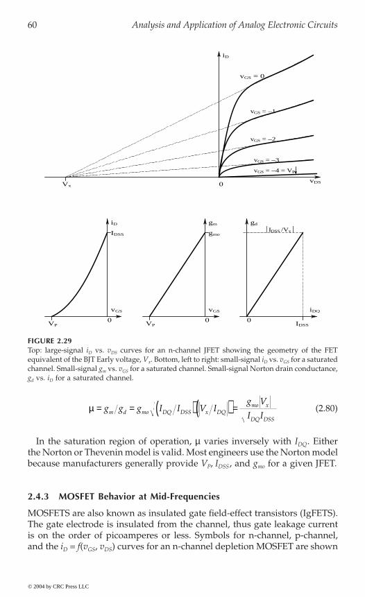
60 Analysis and Application of Analog Electronic Circuits
(2.80)
In the saturation region of operation, m varies inversely with IDQ. Eitherthe Norton or Thevenin model is valid. Most engineers use the Norton modelbecause manufacturers generally provide VP, IDSS, and gmo for a given JFET.
2.4.3 MOSFET Behavior at Mid-Frequencies
MOSFETS are also known as insulated gate field-effect transistors (IgFETS).The gate electrode is insulated from the channel, thus gate leakage currentis on the order of picoamperes or less. Symbols for n-channel, p-channel,and the iD = f(vGS, vDS) curves for an n-channel depletion MOSFET are shown
FIGURE 2.29Top: large-signal iD vs. vDS curves for an n-channel JFET showing the geometry of the FETequivalent of the BJT Early voltage, Vx. Bottom, left to right: small-signal iD vs. vGS for a saturatedchannel. Small-signal gm vs. vGS for a saturated channel. Small-signal Norton drain conductance,gd vs. iD for a saturated channel.
iD
Vx 0
vGS vGS
iD
gmoIDSS
gd
iDQ
VP0 0
IDSS0
VP
IDSS /Vx
vDS
gm
vGS = −2
vGS = −1
vGS = 0
vGS = −3
vGS = −4 = VP
m = = ( ) ( ) =g g g I I V Ig V
I Im d mo DQ DSS x DQmo x
DQ DSS
© 2004 by CRC Press LLC
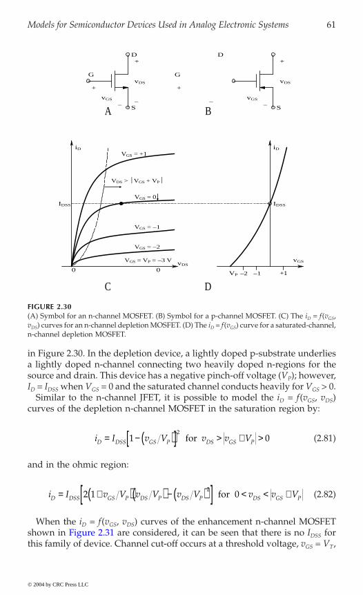
Models for Semiconductor Devices Used in Analog Electronic Systems 61
in Figure 2.30. In the depletion device, a lightly doped p-substrate underliesa lightly doped n-channel connecting two heavily doped n-regions for thesource and drain. This device has a negative pinch-off voltage (VP); however,ID = IDSS when VGS = 0 and the saturated channel conducts heavily for VGS > 0.
Similar to the n-channel JFET, it is possible to model the iD = f(vGS, vDS)curves of the depletion n-channel MOSFET in the saturation region by:
(2.81)
and in the ohmic region:
(2.82)
When the iD = f(vGS, vDS) curves of the enhancement n-channel MOSFETDSS for
this family of device. Channel cut-off occurs at a threshold voltage, vGS = VT,
FIGURE 2.30(A) Symbol for an n-channel MOSFET. (B) Symbol for a p-channel MOSFET. (C) The iD = f(vGS,vDS) curves for an n-channel depletion MOSFET. (D) The iD = f(vGS) curve for a saturated-channel,n-channel depletion MOSFET.
VGS = VP = −3 V
VDS > VGS + VP
IDSS IDSS
VP0 0
vGS
iD iD
+1−1−2
VGS = 0
VGS = +1
VGS = −1
VGS = −2
G G
D D
S
vGS vGS
+ +
++
vDS vDS
vDS
− − −S −
A B
C D
i I v V v v VD DSS GS P DS GS P= - ( )[ ] > + >1 02 for
i I v V v V v V v v VD DSS GS P DS P DS P DS GS P= +( )( ) - ( )[ ] < < +2 1 02
for
© 2004 by CRC Press LLC
shown in Figure 2.31 are considered, it can be seen that there is no I
62 Analysis and Application of Analog Electronic Circuits
where iD reaches some defined low value, e.g., 10 mA. The mathematicalmodel for n-channel enhancement MOSFET iD = f(vGS, vDS) in the saturationregion is:
(2.83)
In the ohmic channel operating region:
(2.84)
The line separating the saturated- and ohmic-channel regions is
IDB = K VDS2 (2.85)
p-channel MOSFETs have iD = f(vGS, vDS) curves with the signs oppositethose for n-channel devices. It is easy to see from Equation 2.73, whichdefines the small-signal transconductance, and Equation 2.72, which definesthe small-signal drain conductance, that all FETs (JFETs, MOSFETs, n-channel,p-channel, enhancement, depletion) have the same parsimonious MFSSM —a case of electronic serendipity.
2.4.4 Basic Mid-Frequency Single FET Amplifiers
Just as in the case of BJTs, there are so-called grounded-source amplifiers,grounded-gate amplifiers, and source followers. In order to find the small-
FIGURE 2.31Left: the iD = f(vGS, vDS) curves for an n-channel enhancement MOSFET. Right: the iD = f(vGS)curve for a saturated-channel, n-channel enhancement MOSFET.
iD iD
vGSVT
0 v DS 0 31 2 4 5 6 7
Saturation regionOhmicregion
vGS = VT = +3 V
vGS = +4 V
vGS = +5 V
vGS = +6 V
vGS = +7 V
i K v V K V v V v V vD GS T T GS T GS T DS= -( ) = -( ) < - <2 2 2
1 0 for
i K v V v v v v VD GS T DS DS DS GS T= -( ) -[ ] < < -2 02 for
© 2004 by CRC Press LLC

Models for Semiconductor Devices Used in Analog Electronic Systems 63
signal voltage gain of each if these amplifiers, as well as their input and
in Figure 2.32. At mid-frequencies, the external coupling and bypass capac-itors are treated as short circuits. Thus, the source is at small-signal ground,so vs = 0. The amplifier’s mid-frequency gain is found from the node equation:
vo [GD + gd] = –gm vgs = –gm v1 (2.86)
Ø
(2.87)
From inspection of the MFSSM of the circuit, Rin Æ • and Rout = RD rd/(RD + rd).
FIGURE 2.32(A) An n-channel JFET “grounded-source” amplifier. CS bypasses small ac signals at the JFET’ssource to ground, making vs = 0. (B) MFSSM of the amplifier. The same MFSSM would obtainif a p-channel JFET were used.
A
B
VDD
RD
vo
vo
D
D
S
S
G
G
v1
RG RS CS
C1
vgs
+
+
+
gmvgs
RGv1 gd GD
−
−
−
Kvv
g r RR rv
o m d D
D d
= =-
+1
© 2004 by CRC Press LLC
output resistances, first examine a JFET grounded-source amplifier, shown
64 Analysis and Application of Analog Electronic Circuits
Next, consider an n-channel MOSFET grounded-gate amplifier at mid-frequencies. The electrical circuit and its MFSSM are shown in Figure 2.33.Write two node equations, one for the vs node and the other for the drain(output) node.
vs [GS + gd + gm] - vo [gd] = v1GS (2.88A)
-vs [gd + gm] + vo [gd + GD] = 0 (2.88B)
Using Cramer’s rule:
D = GS gd + GD [GS + gd + gm] (2.89)
(2.90)
FIGURE 2.33(A) An n-channel MOSFET grounded-gate amplifier. (B) MFSSM of the MOSFET G-G amplifier.See text for analysis.
B
A
RD
gd
vs
RS vs
vo
vo
D
DS
S
RS
v1
v1
+
+
gmvgs
G
G
RD
VDD
vv
R rR r R g r
s D d
D d S m d1 1=
++ + +( )
© 2004 by CRC Press LLC
Models for Semiconductor Devices Used in Analog Electronic Systems 65
(2.91)
The input resistance, Rin, of the MOSFET GG amplifier is found from:
(2.92)
Rout is approximately RD for the GG amplifier.Finally, examine the MOSFET source-follower amplifier at mid-frequen-
to analyze because the drain is at SS ground. The output node equation is:
vo [GC + gd + gm] = gm v1 (2.93)
Equation 2.93 leads to the SF amplifier’s gain:
(2.94)
By inspection, Rin Æ •; Rout can be found by voc/isc.
(2.95)
Single FET amplifiers generally have higher Rin, about the same Rout, lessgain, and more even harmonic distortion than equivalent BJT amplifiers.
2.4.5 Simple Amplifiers Using Two FETs at Mid-Frequencies
As in the case of BJTs, certain basic building blocks for analog ICs can be
field-effect transistors. Notably absent is the difference amplifier; because ofits great importance in analog electronic circuits, the DA is treated separately
which the input transistor is an n-channel MOSFET acting as a voltagecontrol-led current source driving the base of a power npn BJT. Figure 2.35(B)shows the FET–BJT equivalent for the “feedback pair” power amplifier. InFigure 2.35(C), a source-follower/grounded-gate high-frequency amplifiercan be seen and an FET–FET cascode amplifier is shown in Figure 2.35(D).
vv
R g r
R r R g rKo D m d
D d S m dv
1
1
1=
+( )+ + +( ) =
Rvi
v Rv v v
RR r
R r R g r
RR r
g rins
S
s
S
D d
D d S m d
SD d
m d
= =-( ) =
-+
+ + +( )= +
++( )
1 1
1 11 11
1
Kvv
R g rr R g rv
o D m d
d D m d
= =+ +( ) <
1 11
Rvi
v R g rr R g r
g v
R r g r
R r g routoc
sc
D m d
d D m d
m
D d m d
D d m d
= =+ +( ) =
+( )+ +( )
1
1
1 1
1
© 2004 by CRC Press LLC
cies. The circuit and its MFSSM are shown in Figure 2.34. This an easy circuit
made from two transistors. Figure 2.35 illustrates four such circuits using
in Chapter 3 of this text. Figure 2.35(A) illustrates a Darlington amplifier in
66 Analysis and Application of Analog Electronic Circuits
It is necessary first to examine the gain of the FET–BJT Darlington con-
s o
note that ib = gie (vs - vo); vgs = v1 - vs; m = gm rd; and gie = 1/hie.
vs [gd + gie + gm] - vo gie = v1 gm (2.96A)
-vs [gie (1 + hfe)] + vo [gie (1 + hfe) + GE] = 0 (2.96B)
Using Cramer’s rule,
D = (gd + gm)gie (1 + hfe) + GE (gd + gie + gm) (2.97)
Dvo = v1 gm gie (1 + hfe) (2.98)
FIGURE 2.34(A) A p-channel MOSFET source follower. (B) MFSSM for the MOSFET S-F.
v1
v1
gmvgs
RS
RS
−VDD
vo
vo
S
D
D
gdG
G
vgs
Svgs
+
+
+
−
++
−
−
−
−
A
B
RG
RG
© 2004 by CRC Press LLC
nected as an emitter follower. This circuit and its MFSSM are shown in Figure2.36. Analysis begins by writing the node equations for the v and v nodes;

Models for Semiconductor Devices Used in Analog Electronic Systems 67
Solving for vo/v1 yields:
(2.99)
As expected, this voltage gain is <1. The amplifier’s input resistance isextremely high and the output resistance can be found by the open-circuitoutput voltage, given by Equation 2.99, divided by the short-circuit outputcurrent, which is simply ib(1 + hfe) for vo = 0, (Rout = OCV/SCC). Rout is on theorder of single ohms.
Next, find the gain for the FET–BJT feedback pair amplifier shown inFigure 2.35(B). The node equations are:
FIGURE 2.35(A) An n-channel MOSFET/npn BJT Darlington configuration. (B) A p-channel MOSFET/npnBJT feedback pair configuration. (C) An n-channel MOSFET source-follower–grounded-gateamplifier. (D) An n-channel JFET cascode amplifier.
V1
V1
Vo
VDD
VDD
Q1
Q1 Q1Q2 Q2
Q2
VoQ1 Q2
D
S
S
S SS
S
D
D
D D
D
Rg
Rd
Rd
∞RsRg Rg ∞ ∞Rs
(0)
(0)
G
G G
V1 vs
vs
A B
C D
vsV1 vd
v
v
R h
R h h ro E fe
E fe ie d1
1
1 1 1=
+( )+( ) +( ) + +( ) +
m
m m
© 2004 by CRC Press LLC
68 Analysis and Application of Analog Electronic Circuits
vd [gd + gie] - vo [gie] = - v1 gm (2.100A)
-vd [gie (1 + hfe)] + vo [GE + gie (1 + hfe)] = 0 (2.100B)
Using Cramer’s rule,
D = gd [GE + gie (1 + hfe)] + gie GE (2.101)
Dvo = - v1 gm gie (1 + hfe) (2.102)
from which the mid-frequency voltage gain is found:
FIGURE 2.36Top: A MOSFET/BJT Darlington connected as an emitter-follower. Bottom: MFSSM of theDarlington EF. See analysis in text.
RE
RE
vo
vo
hiehfe ib
gd
gmvgs
vs
S
D
GB
ib
VCC
v1
v1
© 2004 by CRC Press LLC
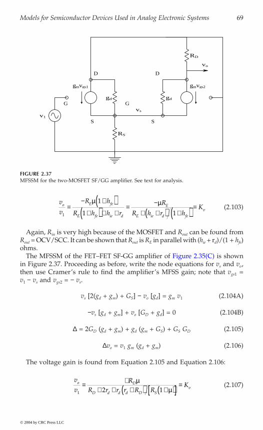
Models for Semiconductor Devices Used in Analog Electronic Systems 69
(2.103)
Again, Rin is very high because of the MOSFET and Rout can be found fromRout = OCV/SCC. It can be shown that Rout is RE in parallel with (hie + rd)/(1 + hfe)ohms.
in Figure 2.37. Proceeding as before, write the node equations for vs and vo,then use Cramer’s rule to find the amplifier’s MFSS gain; note that vgs1 =v1 - vs and vgs2 = - vs.
vs [2(gd + gm) + GS] - vo [gd] = gm v1 (2.104A)
-vs [gd + gm] + vo [GD + gd] = 0 (2.104B)
D = 2GD (gd + gm) + gd (gm + GS) + GS GD (2.105)
Dvo = v1 gm (gd + gm) (2.106)
The voltage gain is found from Equation 2.105 and Equation 2.106:
(2.107)
FIGURE 2.37MFSSM for the two-MOSFET SF/GG amplifier. See text for analysis.
gd gd
vo
vs
RD
gmvgs1 gmvgs2
RS
G G
v1
S S
D D
v
v
R h
R h h r
R
R h r hKo E fe
E fe ie d
E
E ie d fe
v1
1
1 1=
- +( )+( ) + +
= -+ +( ) +( ) =
m m
v
vR
R r r r R RKo D
D d d d D Sv
1 2 1= +
+ + +( ) +( )[ ] =mm
© 2004 by CRC Press LLC
The MFSSM of the FET–FET SF-GG amplifier of Figure 2.35(C) is shown
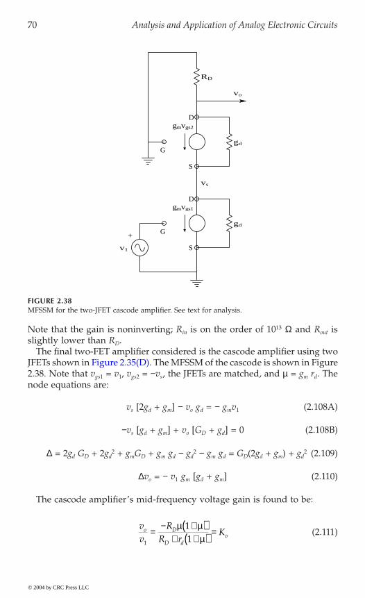
70 Analysis and Application of Analog Electronic Circuits
Note that the gain is noninverting; Rin is on the order of 1013 W and Rout isslightly lower than RD.
The final two-FET amplifier considered is the cascode amplifier using two
2.38. Note that vgs1 = v1, vgs2 = -vs, the JFETs are matched, and m = gm rd. Thenode equations are:
vs [2gd + gm] - vo gd = - gmv1 (2.108A)
-vs [gd + gm] + vo [GD + gd] = 0 (2.108B)
D = 2gd GD + 2gd2 + gmGD + gm gd - gd
2 - gm gd = GD(2gd + gm) + gd2 (2.109)
Dvo = - v1 gm [gd + gm] (2.110)
The cascode amplifier’s mid-frequency voltage gain is found to be:
(2.111)
FIGURE 2.38MFSSM for the two-JFET cascode amplifier. See text for analysis.
gd
gd
RD
vo
vs
gmvgs1
gmvgs2
G
G
v1 S
S
D
D
+
vv
RR r
Ko D
D dv
1
11
=- +( )
+ +( ) =m m
m
© 2004 by CRC Press LLC
JFETs shown in Figure 2.35(D). The MFSSM of the cascode is shown in Figure
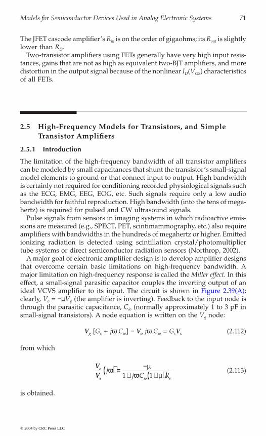
Models for Semiconductor Devices Used in Analog Electronic Systems 71
The JFET cascode amplifier’s Rin is on the order of gigaohms; its Rout is slightlylower than RD.
Two-transistor amplifiers using FETs generally have very high input resis-tances, gains that are not as high as equivalent two-BJT amplifiers, and moredistortion in the output signal because of the nonlinear ID(VGS) characteristicsof all FETs.
2.5 High-Frequency Models for Transistors, and Simple Transistor Amplifiers
2.5.1 Introduction
The limitation of the high-frequency bandwidth of all transistor amplifierscan be modeled by small capacitances that shunt the transistor’s small-signalmodel elements to ground or that connect input to output. High bandwidthis certainly not required for conditioning recorded physiological signals suchas the ECG, EMG, EEG, EOG, etc. Such signals require only a low audiobandwidth for faithful reproduction. High bandwidth (into the tens of mega-hertz) is required for pulsed and CW ultrasound signals.
Pulse signals from sensors in imaging systems in which radioactive emis-sions are measured (e.g., SPECT, PET, scintimammography, etc.) also requireamplifiers with bandwidths in the hundreds of megahertz or higher. Emittedionizing radiation is detected using scintillation crystal/photomultipliertube systems or direct semiconductor radiation sensors (Northrop, 2002).
A major goal of electronic amplifier design is to develop amplifier designsthat overcome certain basic limitations on high-frequency bandwidth. Amajor limitation on high-frequency response is called the Miller effect. In thiseffect, a small-signal parasitic capacitor couples the inverting output of an
clearly, Vo = -mVg (the amplifier is inverting). Feedback to the input node isthrough the parasitic capacitance, Cio (normally approximately 1 to 3 pF insmall-signal transistors). A node equation is written on the Vg node:
Vg [Gs + jw Cio] - Vo jw Cio = GsVs (2.112)
from which
(2.113)
is obtained.
VV
o
s
jj C Rio s
w mw m
( ) = -+ +( )1 1
© 2004 by CRC Press LLC
ideal VCVS amplifier to its input. The circuit is shown in Figure 2.39(A);
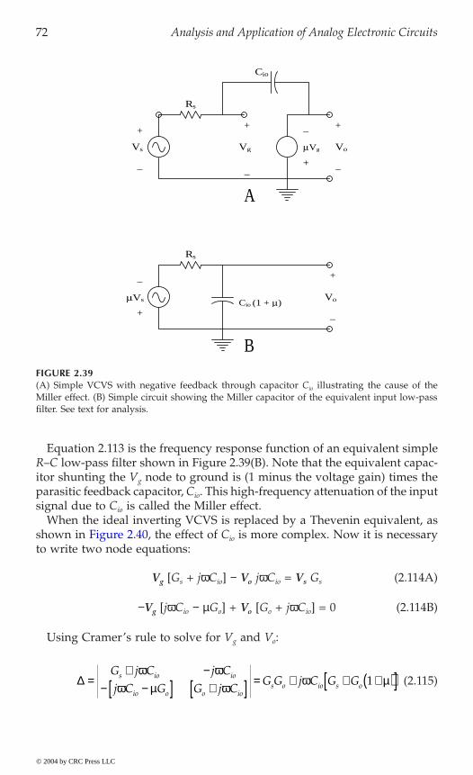
72 Analysis and Application of Analog Electronic Circuits
Equation 2.113 is the frequency response function of an equivalent simpleR–C low-pass filter shown in Figure 2.39(B). Note that the equivalent capac-itor shunting the Vg node to ground is (1 minus the voltage gain) times theparasitic feedback capacitor, Cio. This high-frequency attenuation of the inputsignal due to Cio is called the Miller effect.
When the ideal inverting VCVS is replaced by a Thevenin equivalent, asio
to write two node equations:
Vg [Gs + jwCio] - Vo jwCio = Vs Gs (2.114A)
-Vg [jwCio - mGo] + Vo [Go + jwCio] = 0 (2.114B)
Using Cramer’s rule to solve for Vg and Vo:
(2.115)
FIGURE 2.39(A) Simple VCVS with negative feedback through capacitor Cio illustrating the cause of theMiller effect. (B) Simple circuit showing the Miller capacitor of the equivalent input low-passfilter. See text for analysis.
−
+
µVg Vo
+
−
Cio
Vg
+
−
Rs
Vs
+
−
Rs
Cio (1 + µ)
−
Vo
+
+
−
µVs
A
B
D =+ -
- -[ ] +[ ] = + + +( )[ ]G j C j C
j C G G j CG G j C G Gs io io
io o o ios o io s o
w ww m w w m1
© 2004 by CRC Press LLC
shown in Figure 2.40, the effect of C is more complex. Now it is necessary
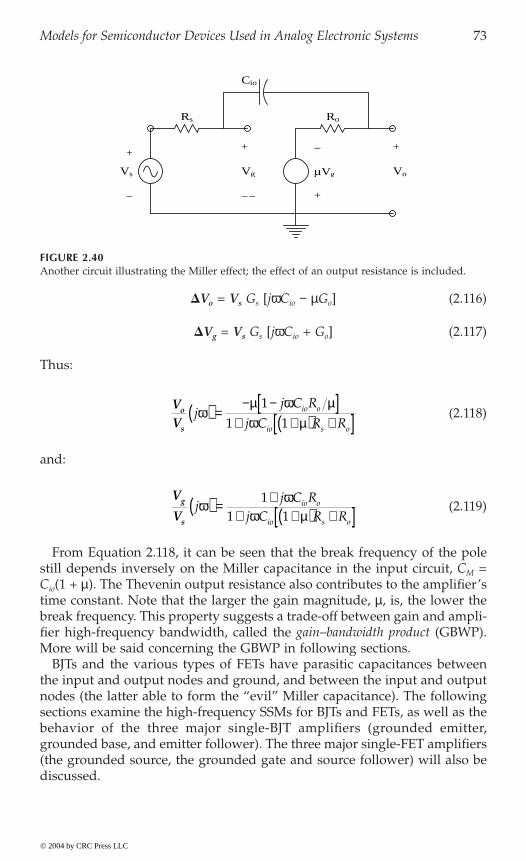
Models for Semiconductor Devices Used in Analog Electronic Systems 73
Vo = Vs Gs [jwCio - mGo] (2.116)
Vg = Vs Gs [jwCio + Go] (2.117)
Thus:
(2.118)
and:
(2.119)
From Equation 2.118, it can be seen that the break frequency of the polestill depends inversely on the Miller capacitance in the input circuit, CM =Cio(1 + m). The Thevenin output resistance also contributes to the amplifier’stime constant. Note that the larger the gain magnitude, m, is, the lower thebreak frequency. This property suggests a trade-off between gain and ampli-fier high-frequency bandwidth, called the gain–bandwidth product (GBWP).More will be said concerning the GBWP in following sections.
BJTs and the various types of FETs have parasitic capacitances betweenthe input and output nodes and ground, and between the input and outputnodes (the latter able to form the “evil” Miller capacitance). The followingsections examine the high-frequency SSMs for BJTs and FETs, as well as thebehavior of the three major single-BJT amplifiers (grounded emitter,grounded base, and emitter follower). The three major single-FET amplifiers(the grounded source, the grounded gate and source follower) will also bediscussed.
FIGURE 2.40Another circuit illustrating the Miller effect; the effect of an output resistance is included.
Ro
Cio
Rs
µVg
−
Vs
++
Vg
+−− −
+
Vo
VV
o
s
jj C R
j C R Rio o
io s o
wm w mw m
( ) =- -[ ]
+ +( ) +[ ]1
1 1
V
Vg
s
jj C R
j C R Rio o
io s o
ww
w m( ) =
++ +( ) +[ ]
11 1
© 2004 by CRC Press LLC
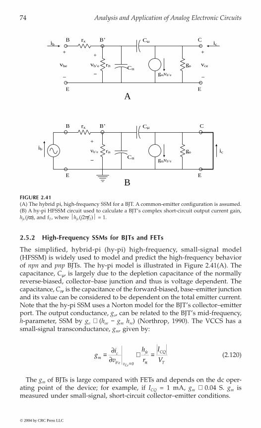
74 Analysis and Application of Analog Electronic Circuits
2.5.2 High-Frequency SSMs for BJTs and FETs
The simplified, hybrid-pi (hy-pi) high-frequency, small-signal model(HFSSM) is widely used to model and predict the high-frequency behaviorof npn and pnp BJTs. The hy-pi model is illustrated in Figure 2.41(A). Thecapacitance, Cm, is largely due to the depletion capacitance of the normallyreverse-biased, collector–base junction and thus is voltage dependent. Thecapacitance, Cp, is the capacitance of the forward-biased, base–emitter junctionand its value can be considered to be dependent on the total emitter current.Note that the hy-pi SSM uses a Norton model for the BJT’s collector–emitterport. The output conductance, go, can be related to the BJT’s mid-frequency,h-parameter, SSM by go @ (hoe - gm hre) (Northrop, 1990). The VCCS has asmall-signal transconductance, gm, given by:
(2.120)
The gm of BJTs is large compared with FETs and depends on the dc oper-ating point of the device; for example, if ICQ = 1 mA, gm @ 0.04 S. gm ismeasured under small-signal, short-circuit collector–emitter conditions.
FIGURE 2.41(A) The hybrid pi, high-frequency SSM for a BJT. A common-emitter configuration is assumed.(B) A hy-pi HFSSM circuit used to calculate a BJT’s complex short-circuit output current gain,hfe (jw), and fT, where Ωhfe (j2pfT)Ω = 1.
C
E
rp Cpvb’e
+
-
Cm
gmvb’e
go
ib ic
vbe vce
+
-
B rx B’
icib
rx
rp
Cm
Cp gmvb’e
govb’e
+
-
B’B
E
+
E
A
B
E
C
-
gi
v
h
r
I
Vmc
b e v
fe CQ
TCe
=∂∂
@ =¢ = 0 p
© 2004 by CRC Press LLC
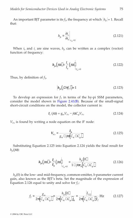
Models for Semiconductor Devices Used in Analog Electronic Systems 75
An important BJT parameter is its fT, the frequency at which hfe = 1. Recallthat:
(2.121)
When ib and ic are sine waves, hfe can be written as a complex (vector)function of frequency:
(2.122)
Thus, by definition of fT,
(2.123)
To develop an expression for fT in terms of the hy-pi SSM parameters,
short-circuit conditions on the model, the collector current is:
Ic (jw) = gmVb¢e - jwCmVb¢e (2.124)
Vb¢e is found by writing a node equation on the B¢ node:
(2.125)
Substituting Equation 2.125 into Equation 2.124 yields the final result forhfe(jw):
(2.126)
hfe(0) is the low- and mid-frequency, common-emitter, h-parameter currentgain, also known as the BJT’s beta. Set the magnitude of the expression ofEquation 2.126 equal to unity and solve for fT:
(2.127)
hiifec
b vce
=∂∂
= 0
hfe jII
jc
b Vce
w w( ) = ( )= 0
hfe j fT2 1p( ) ∫
VIb
¢ =+ +( )b e g j C Cp p mw
hIIfe
c
b
j jh
j r C CV
fe
ce
w ww p p m
( ) = ( ) =( )
+ +( )= 0
0
1
fg
C C
h
C C r
I
C C VTm fe CQ
T
=+( ) =
( )+( ) =
+( )2
0
2 2p p pp m p m p p m
Hz
© 2004 by CRC Press LLC
consider the model shown in Figure 2.41(B). Because of the small-signal
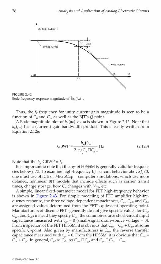
76 Analysis and Application of Analog Electronic Circuits
Thus, the fT frequency for unity current gain magnitude is seen to be afunction of Cp and Cm, as well as the BJT’s Q-point.
A Bode magnitude plot of hfe(jw) vs. w is shown in Figure 2.42. Note thathfe(jw) has a (current) gain-bandwidth product. This is easily written fromEquation 2.126:
(2.128)
Note that the hfe GBWP = fT.It is important to note that the hy-pi HFSSM is generally valid for frequen-
cies below fT/3. To examine high-frequency BJT circuit behavior above fT/3,one must use SPICE or MicroCap‘ computer simulations, which use moredetailed, nonlinear BJT models that include effects such as carrier transittimes, charge storage, how Cp changes with VCB, etc.
A simple, linear fixed-parameter model for FET high-frequency behavior
quency response, the three voltage-dependent capacitances, Cgs, Cgd, and Cds,are assigned values determined from the FET’s quiescent operating point.Manufacturers of discrete FETs generally do not give specific values for Cgs,Cgd, and Cds; instead they specify Ciss, the common-source short-circuit inputcapacitance measured with vds = 0 (small-signal drain–source voltage = 0).From inspection of the FET HFSSM, it is obvious that Ciss = Cgd + Cgs, at somespecific Q-point. Also given by manufacturers is Crss, the reverse transfercapacitance measured with vgs = 0. From the HFSSM, it is obvious that Crss =Cds + Cgd. In general, Cgd Cds, so Crss @ Cgd and Cgs @ Ciss - Crss.
FIGURE 2.42Bode frequency response magnitude of Ωhfe (jw)Ω.
20 loghfe(jω)
− 3 dB
ωωT
ωβ
0 dB
20 log[hfe(0)]
−6 dB/octave
GBWP Hz=( )
+( )h
r C Cfe 0
2p p p m
© 2004 by CRC Press LLC
is shown in Figure 2.43. For simple modeling of FET amplifier high-fre-
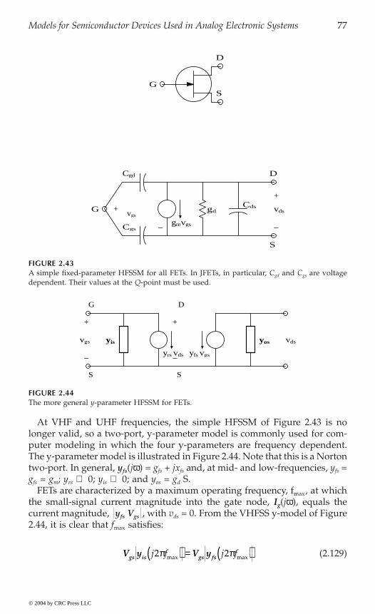
Models for Semiconductor Devices Used in Analog Electronic Systems 77
At VHF and UHF frequencies, the simple HFSSM of Figure 2.43 is nolonger valid, so a two-port, y-parameter model is commonly used for com-puter modeling in which the four y-parameters are frequency dependent.The y-parameter model is illustrated in Figure 2.44. Note that this is a Nortontwo-port. In general, yfs(jw) = gfs + jxfs and, at mid- and low-frequencies, yfs =gfs = gm; yrs Æ 0; yis Æ 0; and yos = gd S.
FETs are characterized by a maximum operating frequency, fmax, at whichthe small-signal current magnitude into the gate node, Ig(jw), equals thecurrent magnitude, yfs Vgs , with vds = 0. From the VHFSS y-model of Figure2.44, it is clear that fmax satisfies:
(2.129)
FIGURE 2.43A simple fixed-parameter HFSSM for all FETs. In JFETs, in particular, Cgd and Cgs are voltagedependent. Their values at the Q-point must be used.
FIGURE 2.44The more general y-parameter HFSSM for FETs.
Cgd
D
D
S
G
Cgsgmvgs
gdCds
G
vgs+
S
−
vds
+
−
yfs vgsyrs vds
yis yosvgs vds
+ +
− −
S S
G D
V y V ygs is gs fsj f j f2 2p pmax max( ) = ( )
© 2004 by CRC Press LLC
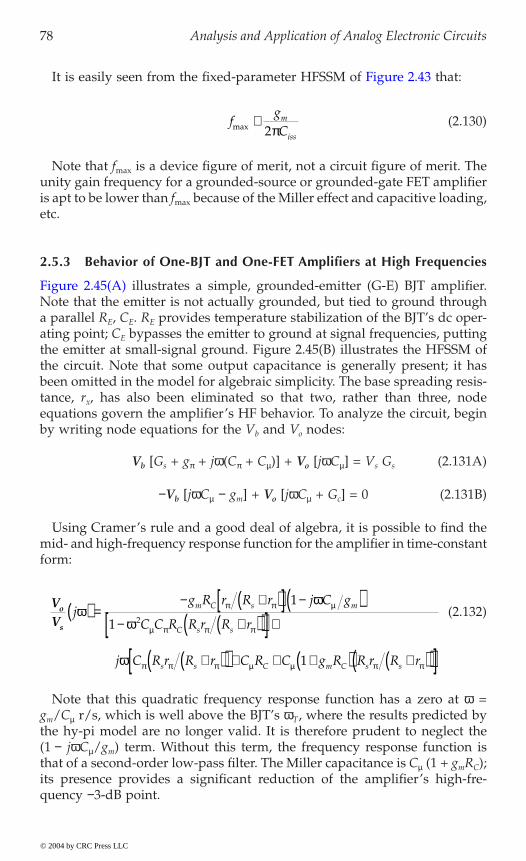
78 Analysis and Application of Analog Electronic Circuits
(2.130)
Note that fmax is a device figure of merit, not a circuit figure of merit. Theunity gain frequency for a grounded-source or grounded-gate FET amplifieris apt to be lower than fmax because of the Miller effect and capacitive loading,etc.
2.5.3 Behavior of One-BJT and One-FET Amplifiers at High Frequencies
Note that the emitter is not actually grounded, but tied to ground througha parallel RE, CE. RE provides temperature stabilization of the BJT’s dc oper-ating point; CE bypasses the emitter to ground at signal frequencies, puttingthe emitter at small-signal ground. Figure 2.45(B) illustrates the HFSSM ofthe circuit. Note that some output capacitance is generally present; it hasbeen omitted in the model for algebraic simplicity. The base spreading resis-tance, rx, has also been eliminated so that two, rather than three, nodeequations govern the amplifier’s HF behavior. To analyze the circuit, beginby writing node equations for the Vb and Vo nodes:
Vb [Gs + gp + jw(Cp + Cm)] + Vo [jwCm] = Vs Gs (2.131A)
-Vb [jwCm - gm] + Vo [jwCm + Gc] = 0 (2.131B)
Using Cramer’s rule and a good deal of algebra, it is possible to find themid- and high-frequency response function for the amplifier in time-constantform:
(2.132)
Note that this quadratic frequency response function has a zero at w =gm/Cm r/s, which is well above the BJT’s wT, where the results predicted bythe hy-pi model are no longer valid. It is therefore prudent to neglect the(1 - jwCm/gm) term. Without this term, the frequency response function isthat of a second-order low-pass filter. The Miller capacitance is Cm (1 + gmRC);its presence provides a significant reduction of the amplifier’s high-fre-quency -3-dB point.
fgCm
issmax @
2p
VV
o
s
jg R r R r j C g
C C R R r R r
j C R r R r C R C g R R r R r
m C s m
C s s
s s C m C s s
ww
w
w
p p m
m p p p
p p p m m p p
( ) =- +( )[ ] -( )
- +( )( )[ ] +
+( )( ) + + +( ) +( )( )[ ]
1
1
1
2
© 2004 by CRC Press LLC
It is easily seen from the fixed-parameter HFSSM of Figure 2.43 that:
Figure 2.45(A) illustrates a simple, grounded-emitter (G-E) BJT amplifier.
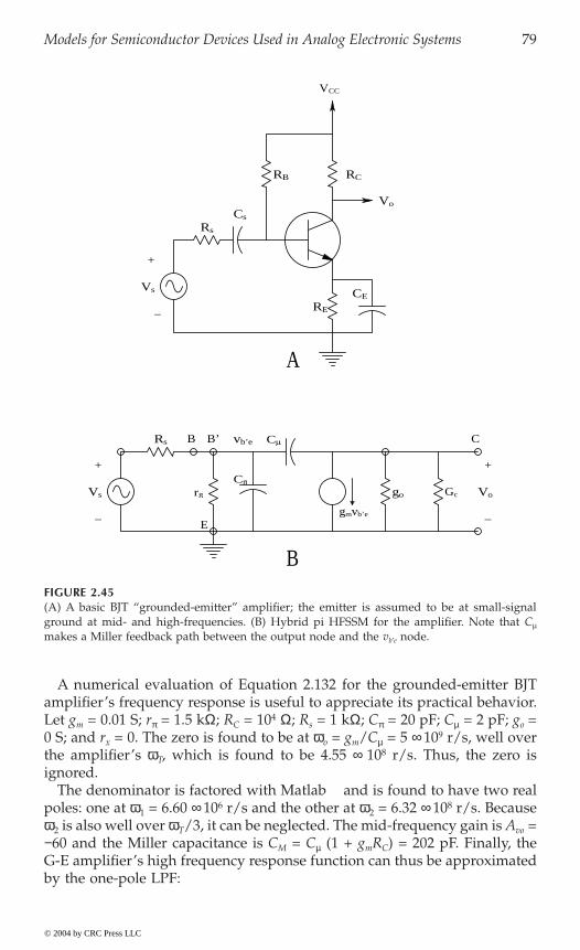
Models for Semiconductor Devices Used in Analog Electronic Systems 79
A numerical evaluation of Equation 2.132 for the grounded-emitter BJTamplifier’s frequency response is useful to appreciate its practical behavior.Let gm = 0.01 S; rp = 1.5 kW; RC = 104 W; Rs = 1 kW; Cp = 20 pF; Cm = 2 pF; go =0 S; and rx = 0. The zero is found to be at wo = gm/Cm = 5 ¥ 109 r/s, well overthe amplifier’s wT, which is found to be 4.55 ¥ 108 r/s. Thus, the zero isignored.
The denominator is factored with Matlab‘ and is found to have two realpoles: one at w1 = 6.60 ¥ 106 r/s and the other at w2 = 6.32 ¥ 108 r/s. Becausew2 is also well over wT/3, it can be neglected. The mid-frequency gain is Avo =-60 and the Miller capacitance is CM = Cm (1 + gmRC) = 202 pF. Finally, theG-E amplifier’s high frequency response function can thus be approximatedby the one-pole LPF:
FIGURE 2.45(A) A basic BJT “grounded-emitter” amplifier; the emitter is assumed to be at small-signalground at mid- and high-frequencies. (B) Hybrid pi HFSSM for the amplifier. Note that Cm
makes a Miller feedback path between the output node and the vb¢e node.
VCC
RB RC
Vo
Rs
Cs
A
RE
CEVs
+
−
B
Rs B B’ Cµ C
go Gc
gmvb’e
Vo
+
−
Vs rπ
vb’e
Cπ
+
− E
© 2004 by CRC Press LLC
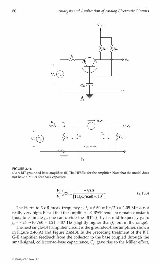
80 Analysis and Application of Analog Electronic Circuits
(2.133)
The Hertz to 3-dB break frequency is fx = 6.60 ¥ 106/2p = 1.05 MHz, notreally very high. Recall that the amplifier’s GBWP tends to remain constant;thus, to estimate fx, one can divide the BJT’s fT by its mid-frequency gain:fx ˆ = 7.24 ¥ 107/60 = 1.21 ¥ 106 Hz (slightly higher than fx, but in the range).
The next single-BJT amplifier circuit is the grounded-base amplifier, shownin Figure 2.46(A) and Figure 2.46(B). In the preceding treatment of the BJTG-E amplifier, feedback from the collector to the base coupled through thesmall-signal, collector-to-base capacitance, Cm
, gave rise to the Miller effect,
FIGURE 2.46(A) A BJT grounded-base amplifier. (B) The HFSSM for the amplifier. Note that the model doesnot have a Miller feedback capacitor.
B,B’
Rs
Rs
gmveve
Cµrπ
Cπ GC
CB
RBRC
Vo
Vs
+
−
VCC
Vs
+
−
Vo
A
B
vb’e = −ve
VV
o
s
jj
ww
( ) @ -+ ¥( )
60 01 6 60 106
..
© 2004 by CRC Press LLC
Models for Semiconductor Devices Used in Analog Electronic Systems 81
which caused a lowered high-frequency response. In the grounded-base(G-B) amplifier, no such feedback occurs and no Miller effect is present.Consequently, a G-B amplifier’s high-frequency response is generally betterthan that for a G-E amplifier, other conditions being equal.
To begin analysis of the G-B amplifier, note that the transistor’s base isbypassed to ground, causing the small-signal vb = 0. Thus, Vb¢e = Vbe = Vb -Ve = Ve. Assume that rx and go = 0 for algebraic simplicity. Using the hy-piHFSSM for the BJT, write node equations for the Ve and Vo nodes:
Ve [Gs + gp + gm + jwCp ] = Vs Gs (2.134A)
Vo [GC + jwCm] - Ve gm = 0 (2.134B)
Because the two node equations are independent, it is simple to write:
(2.135)
(2.136)
Substitute Equation 2.135 into Equation 2.136 and find the G-B amplifier’sfrequency response function:
(2.137)
Now evaluate the frequency response function’s parameters. Let Rs =200 W; rp = 2 kW; gm = 0.01; RC = 104 W; Cm = 2 pF; Cp = 20 pF; rx = 0; and go = 0.From these parameters, find the noninverting, mid-frequency gain, Avo =+32.26; w1 = 1/(RCCm) = 5 ¥ 107 r/s; w2 = [1 + Rs (gp + gm)]/RsCp] = 7.75 ¥ 108
r/s; and wT = 4.55 ¥ 108 r/s. Disregard w2 because it is above wT. Thus, theapproximate frequency response function for the G-B BJT amplifier is:
(2.138)
The GBWP for this amplifier is 32.27 ¥ 5 ¥ 107 = 1.61 ¥ 109 r/s. Clearly, theG-B amplifier has improved high-frequency response because no Millereffect is present.
The final BJT amplifier to be considered is the emitter-follower (E-F) orgrounded-collector amplifier. An E–F amplifier and its HFSSM are shown in
VV
es=
+ +( ) +1 R g g j C Rs m sp pw
VV
oe=
+g R
j C Rm C
C1 w m
VV
o
s
jg R R g g
j C R j C R R g g
m C s m
C s s m
ww w
p
m p p
( ) =+ +( )[ ]
+( ) + + +( )[ ] 1
1 1 1
VV
o
s
jj
ww
( ) @ ++ ¥( )
32 261 5 107
.
© 2004 by CRC Press LLC
82 Analysis and Application of Analog Electronic Circuits
Figure 2.47. Node equations are written for the Vb and the Vo = Ve nodes.Assume that Rb Rs and rx = go = 0. Also, Vb¢e = Vbe = (Vb - Vo).
(2.139A)
(2.139B)
FIGURE 2.47(A) A BJT emitter-follower. (B) The HFSSM for the amplifier.
RB
RE
Rs
Vo
RE Vo
rπCπ
gmvb’eVs
Vs
+
+
+
+−
−
−
−VCC
B B’Rs Cµ C
E
−
Cs
Co
A
B
V G g s C C V g sC V Gb s o s s+( ) + +( )[ ] - +[ ] =p m p p p
- +( ) +[ ] + + +( ) +[ ] =V g g sC V G g g sCb m o E mp p p p 0
© 2004 by CRC Press LLC

Models for Semiconductor Devices Used in Analog Electronic Systems 83
From Cramer’s rule:
(2.140)
(2.141)
The emitter follower’s frequency response function can then be written,letting s Æ jw:
(2.142)
Note that the preceding frequency response function is not in time-constantformat; to put in standard TC format, one must divide all terms by [1 + RE
(gm + gp)] + gp Rs. The mid-frequency gain of the E-F amplifier is simply:
(2.143)
Note that no Miller effect is present in an E-F amplifier, as well as nofeedback from output to input; the gain is positive and <1. Let Cm = 2 pF;Cp = 20 pF; gm = 0.01 S; gp = 5 ¥ 10-4 S; Rs = 200 W; and RE = 104 W. Thefrequency of the zero is 5.25 ¥ 108 r/s and it can be neglected. The E-F’s poles(break frequencies) are found to be at 2.058 ¥ 109 r/s and 4.102 ¥ 109 r/s.wT = 4.55 ¥ 108 r/s. Because the break frequencies are 10 times the transistor’swT, the results are not particularly valid. What they do illustrate, however,is that the E-F has amazing bandwidth. Capacitance shunting GC (outputcapacitance) will lower the E-F’s high frequency response.
It is now appropriate to consider the high-frequency behavior of the threeFET amplifiers analogous to the BJT amplifiers described previously: the FETgrounded-source (G-S) amplifier; the grounded-gate (G-G) amplifier; and
its HFSSM. It is clear that there will be a Miller effect for this amplifierbecause it has an inverting gain with magnitude >1 and a small capacitanceCgd coupling the output node to the input. The node equations for the G-Samplifier’s HFSSM are:
Vg [G1 + s(Cgs + Cgd)] - Vo[sCgd] = V1 G1 (2.144A)
-Vg[-gm + sCgd] + Vo[GD¢ + s(Cds + Cgd)] = 0 (2.144B)
DV V G g g sCo s s m= +( ) +[ ]p p
D = + +( ) + + +( )[ ] + + +( ) +s C C s C G G C G g g G G g g g Gs E E m s E m E2
p m p m p p p
VV
sR g g sC g g
s C C R R s C R R C R R g g
R g g g R
o
s
E m m
E s E s s E m
E m s
( ) =+( ) + +( )[ ]
+ +( ) + + +( )[ ] +
+ +( ) +
p p p
p m p m p
p p
1
1
1
2
AR g r
R g r R rvoE m
E m s
=+( )
+( ) + +<
11
1p
p p
© 2004 by CRC Press LLC
the source follower (S-F). Figure 2.48 illustrates a typical G-S amplifier and
84 Analysis and Application of Analog Electronic Circuits
where GD¢ = GD + gd. These equations are solved with Cramer’s rule:
D = G1 GD¢+ s(Cds + Cgd)G1 + s(Cgs + Cgd)GD¢ + s2 [(Cgs + Cgd)Cds + Cgd Cgs] (2.145)
DVo = V1 G1 [-gm + sCgd] (2.146)
Thus, the detailed frequency response function for the FET G-S amplifier is:
(2.147)
FIGURE 2.48(A) A JFET grounded-source amplifier. (B) The HFSSM for the amplifier.
RG
RS
CS
R1
C1
RD
RDrdCds
gmvgs
Cgd
Cgs
Vo
Vo
Vg
S
DG
V1
+
+
−
−
VDD
A
B
V1
−
+
R1
VV
sg R sC g
s C C C C C R R
s R C g R R C C R C
o m D gd m
gs gd ds gd gs D
gd m D D gd ds gs
12
1
1 1
1
1 1
( ) =- ¢ -[ ]
+( ) +[ ] ¢ +
+ ¢( ) + ¢ +( ) +[ ] +
© 2004 by CRC Press LLC

Models for Semiconductor Devices Used in Analog Electronic Systems 85
Pick some reasonable parameters for the JFET: gd = 2 ¥ 10-5 S; IDSS = 10 mA;IDQ = 5 mA; gmo = 7 ¥ 10-3 S; Cgs = Cgd = 2.5 pF; Cds = 0.5 pF; R1 = 600 W; andRD = 3 kW. Thus, G ¢D = 3.533 ¥ 10-4 S and gm = gmo = 4.243 ¥ 10-3 S.
Now the zero is at gm/Cgd = 1.70 ¥ 109 r/s, which is ridiculously high, soneglect it. The mid-frequency gain is simply Avo = gmR¢D = -12.0. To find theG-S amplifier’s two break frequencies (poles), it is necessary to factor thedenominator of Equation 2.147. The two break frequencies are found to bew1 = 3.451 ¥ 107 r/s, or 5.492 ¥ 106 Hz, and w2 = 1.950 ¥ 109 r/s. The first,lower-frequency pole is dominant and the second pole is neglected, givingthe approximate frequency response for the G-S amplifier:
(2.148)
The FET analog to the BJT grounded-base circuit is the FET grounded-gateDQ flows through Rs
and V1, self-biasing the Q point of the JFET so that VGSQ is appropriatelynegative. Figure 2.49(B) shows the HFSSM of the G-G amplifier. Write nodeequations at Vs and Vo:
(2.149A)
(2.149B)
Using Cramer’s rule:
(2.150)
(2.151)
The frequency response function for the JFET G-G amplifier can finally bewritten after some algebra:
IDQ IDSS§( )
VV
o
1
jj
ww
( ) @ -+ ¥( )[ ]
12
1 3 451 107.
V G g g s C C V g sC V Gs s d m gs ds o d ds s+ + + +( )[ ] - +[ ] = 1
- + +[ ] + + + +( )[ ] =V g g sC V G g s C Cs m d ds o D d dg ds 0
D = +( ) +[ ]+ +( ) + +( ) +( ) +[ ]+ +( ) + +( )[ ]
s C C C C C
s G C C g C C G C C g C
G G g G g g
ds dg gs gs dg
s dg ds d ds gs D ds gs m dg
s D d D d m
2
DV V G g g sCo s m d ds= + +[ ]1
© 2004 by CRC Press LLC
amplifier, shown in Figure 2.49(A). Assume that the dc I
86 Analysis and Application of Analog Electronic Circuits
(2.152)
The numerical values of the FET HFSSM parameters are the same as forthe G-S amplifier: gd = 2 ¥ 10-5 S; IDSS = 10 mA; IDQ = 5 mA; gmo = 7 ¥ 10-3 S;
FIGURE 2.49(A) A JFET grounded-gate amplifier. (B) The HFSSM for the amplifier.
VDD
RD
RD
Cgs Cgd
gmvgs
gd
DCds
S
G
Rs
Vo
Rs
B
A
+
++
− −
Vs
V1
V1
−
Vo
S D
G
VV
sR g g sC r g r
s C C C C C R R
s G C C G g C C g C
g R R g g
o D m d ds d m d
ds dg gs gs dg s D
s dg ds D d ds gs m dg
d D s d m
12
1 1
1
( ) =+ +( ) + +( )[ ]
+( ) +[ ] +
+( ) + +( ) +( ) +[ ] +
+ + +( )[ ]
º
© 2004 by CRC Press LLC
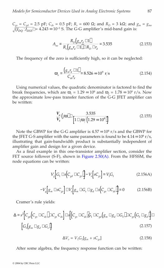
Models for Semiconductor Devices Used in Analog Electronic Systems 87
Cgs = Cgd = 2.5 pF; Cds = 0.5 pF; Rs = 600 W; and RD = 3 kW; and gm = gmo
= 4.243 ¥ 10-3 S. The G-G amplifier’s mid-band gain is:
(2.153)
The frequency of the zero is sufficiently high, so it can be neglected:
(2.154)
Using numerical values, the quadratic denominator is factored to find thebreak frequencies, which are w1 = 1.29 ¥ 108 and w2 = 1.78 ¥ 109 r/s. Nowthe approximate low-pass transfer function of the G-G JFET amplifier canbe written:
(2.155)
Note the GBWP for the G-G amplifier is 4.57 ¥ 108 r/s and the GBWP forthe JFET G-S amplifier with the same parameters is found to be 4.14 ¥ 108 r/s,illustrating that gain-bandwidth product is substantially independent ofamplifier gain and design for a given device.
As a final example in this one-transistor amplifier section, consider the
node equations can be written:
(2.156A)
(2.156B)
Cramer’s rule yields:
DVo = V1G1[gm + sCgs] (2.158)
After some algebra, the frequency response function can be written:
IDQ IDSS§( )
AR g r
R g r R rvoD m d
s m d D d
=+( )
+( ) + +=
1
13 535.
wom d
ds d
g r
C r=
+( ) = ¥1
8 526 109. r s
VV
o
1
jj
ww
( ) @+ ¥( )[ ]
3 535
1 1 29 108
.
.
V G s C C V sC V Gg gd gs o gs1 1 1+ +( )[ ] - [ ] =
- +[ ] + + + + +( )[ ] =V g sC V g G g s C Cg m gs o m s d gs ds 0
D = +( ) +[ ] + +( ) + + +( ) + +( )[ ] +
+ +( )[ ]s C C C C C s C C G C g g G C G g
G g g G
gd gs ds gs ds gs ds gd m d S gs S d
m d s
21
1 (2.157)
© 2004 by CRC Press LLC
FET source follower (S-F), shown in Figure 2.50(A). From the HFSSM, the
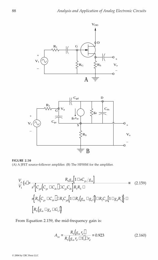
88 Analysis and Application of Analog Electronic Circuits
(2.159)
From Equation 2.159, the mid-frequency gain is:
(2.160)
FIGURE 2.50(A) A JFET source-follower amplifier. (B) The HFSSM for the amplifier.
R1
R1
V1
V1
RG
VDD
gd
Cds
Cgs
Cgd
S
D
D
RS Vo
G
+
+
+
+
RS Vo
− −
−
−
A
B
gmvgs
G Vg
VV
sR g sC g
s C C C C C R R
s R C C R C R g g R C g R
R g g G
o S m gs m
gd gs ds gs ds S
S gs ds gd S m d gs d s
S m d s
12
1
1 1
1
1 1
( ) =+[ ]
+( ) +[ ] +
+( ) + + +( )[ ] + +[ ] +
+ +( )[ ]
º
AR g r
R g r rvoS m d
S m d d
= ( )+( ) +
=1
0 923.
© 2004 by CRC Press LLC

Models for Semiconductor Devices Used in Analog Electronic Systems 89
using the parameters of the preceding FET amplifiers. The zero is at wo =gm/Cgs = 1.70 ¥ 109 r/s.
The two poles found by factoring the quadratic denominator in numericalform are w1 = 1.26 ¥ 109 and w2 = 5.96 ¥ 108 r/s. Thus, the approximate mid-and high-frequency response of the JFET S-F is:
(2.161)
This section has shown how the Miller effect reduces high-frequencyresponse in conventional grounded-emitter BJT amplifiers and grounded-source FET amplifiers. It has also shown that G-B, G-G, E-F, and S-F amplifiersdo not suffer from the Miller effect and generally have their first high-frequency break frequency well above that for the same transistors used inG-E and G-S amplifiers. The following section shows that good high-frequencyamplifiers essentially free of Miller effect can be made using two transistors.
2.5.4 High-Frequency Behavior of Two-Transistor Amplifiers
The loss of high-frequency amplification from the Miller effect comes fromthe negative feedback from output to input nodes supplied through the smalldrain-to-gate capacitance in FETs or through the collector-to-base capaci-tance in BJTs, configured as G-S and G-E amplifiers, respectively. Clearly, agood high-frequency amplifier design must avoid the Miller effect at all costs.
The first broadband amplifier configuration can be realized with two BJTs,two FETs, or an FET and a BJT. It is called the emitter-follower/grounded-base
circuit and its HFSSM. As in the previous examples of single-transistor, high-frequency amplifier analysis, write the three node equations for the HFSSMof the amplifier:
(2.162A)
(2.162B)
(2.162C)
Note that the Vo node equation is depends only on Ve; thus:
(2.163)
VV
o
1
jj
ww
( ) @ ++ ¥( )[ ]
0 923
1 5 96 108
.
.
V G sC g Vo C m e+[ ] - =m 2 2 0
V G g s C C V g sC V Gb s e s s+ + +( )[ ] - +[ ] =p m p p p1 1 1 1
- + +[ ] + + + +( ) + + +( )[ ] =V g g sC V g g g g G s C Cb m e m m E1 1 1 1 2 1 2 1 2 0p p p p p p
VV
sg RsC R
o
e
m C
C
( ) =+
2
21 m
© 2004 by CRC Press LLC
(EF–GB) configuration when made from BJTs. Figure 2.51 illustrates the
90 Analysis and Application of Analog Electronic Circuits
To simplify the algebra, assume the transistors are identical and have thesame ICQ. Thus,
(2.164)
and, using Cramer’s rule and a plethora of algebra, the frequency responsefor Ve can be found (let s = jw):
FIGURE 2.51(A) A BJT emitter-follower–grounded-base amplifier. (B) The HFSSM for the amplifier.
RE
RE
rp1
rp2
Cp1
Cp2
RC
RCRB RB
Rs
Cm2
B2, B2’
E2
A
B
Vs
-
VCC
Q2
Cs
gm1vb’e1
Ve
gm2vb’e2
Ve E1
B1, B1’ Vb
-
+
Vs
Rs Cm1 C2C1 Vo
Q1
Vo
+ Ve
CB2
C C C g g g r r r C C C
r r g g
m m m
x x o o
p p p p p p m m m1 2 1 2 1 2 1 2
1 2 1 20 0
= = = = = = = =
= = = =
, , , ,
, and
© 2004 by CRC Press LLC
Models for Semiconductor Devices Used in Analog Electronic Systems 91
(2.165)
The mid-frequency gain of the amplifier is found by substituting Equation2.165 into Equation 2.163 and letting s = jw = 0:
(2.166)
Note that the small-signal term, gm rp, is equal to the BJT’s beta or hfe. Definereasonable numerical values for the EF–GB circuit’s parameters: ICQ = 1 mA;gm = 0.0384615 S; rp = 2.6 ¥103 W; Rs = 300 W; RC = 6 kW; RE = 3 kW; Cm = 2 pF;and Cp = 200 pF.
Substituting these parameters in the preceding expressions yields Avo = +108.66. The frequency of the zero is wo = (1 + gm rp)/Cp rp = 1.942 ¥ 108 r/s.The collector break frequency is at w3 = 1/CmRC = 8.333 ¥ 107 r/s. The othertwo break frequencies are found from finding the roots of the denominatorof Equation 2.165; they are w1 = 1.961 ¥ 108 and w2 = 3.438 ¥ 107 r/s. Thusthe overall frequency response function for the EF–GB amplifier is:
Note that the HF pole nearly cancels the HF zero, so the final (approximate)frequency response is
(2.168)
Note from the HFSSM of the EF–GB amplifier that it has no Miller capacitancecoupling the output to the input and the gain is noninverting. By way ofcomparison, substitute the hy-pi transistor model parameters used previouslyinto the frequency response expression for a conventional single G-E ampli-fier, given by Equation 2.132 in the previous section. The mid-frequency gainfor this amplifier is found to be -230.8 and the dominant break frequency isat w1 = 5.348 ¥ 106 r/s, considerably lower that that for the EF–GB amplifier.
VV
sg r sC r g r
s C C C R r
s C r R g r G r C R g r G r
g r G r R g
e
s
m m
s
s m E s m E
m E s m
( ) =+( ) + +( )[ ]
+[ ] +
+ + +( )[ ] + +( ) +[ ] +
+( ) + +
1 1 1
2
2 2 2 1
2 1
2 2
p p p p
p m p p
p p p p m p p
p p ++( )[ ]GE
AVV
g R
r R g R R g rvoo
s
m C
s m E E m
= =+ + +( )[ ] +( )[ ]2 1 1p p
VV
o
s
jj
j j jw
w
w w w( ) =
+ + ¥( )[ ]+ ¥( )[ ] + ¥( )[ ] + ¥( )[ ]
108 66 1 1 942 10
1 3 438 10 1 8 333 10 1 1 961 10
8
7 7 8
. .
. . .
(2.167)
VV
o
s
jV
V j jo
s
ww w
( ) @+
+ ¥( )[ ] + ¥( )[ ]108 66
1 3 438 10 1 8 333 107 7
.
. .
© 2004 by CRC Press LLC
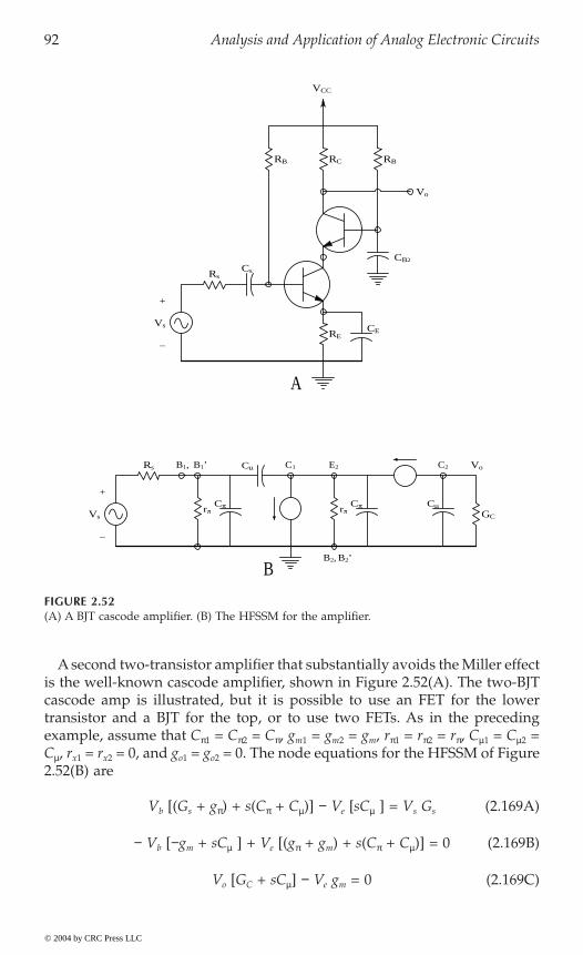
92 Analysis and Application of Analog Electronic Circuits
A second two-transistor amplifier that substantially avoids the Miller effectis the well-known cascode amplifier, shown in Figure 2.52(A). The two-BJTcascode amp is illustrated, but it is possible to use an FET for the lowertransistor and a BJT for the top, or to use two FETs. As in the precedingexample, assume that Cp1 = Cp2 = Cp, gm1 = gm2 = gm, rp1 = rp2 = rp, Cm1 = Cm2 =Cm, rx1 = rx2 = 0, and go1 = go2 = 0. The node equations for the HFSSM of Figure2.52(B) are
Vb [(Gs + gp) + s(Cp + Cm)] - Ve [sCm ] = Vs Gs (2.169A)
- Vb [-gm + sCm ] + Ve [(gp + gm) + s(Cp + Cm)] = 0 (2.169B)
Vo [GC + sCm] - Ve gm = 0 (2.169C)
FIGURE 2.52(A) A BJT cascode amplifier. (B) The HFSSM for the amplifier.
RB RBRC
RE
CB2
CsRs
Rs
CE
Vo
VoC2
B2, B2’
C1 E2B1, B1’
rπ rπCπ Cπ
Cµ
CµGC
VCC
Vs
Vs
+
+
−
−
A
B
© 2004 by CRC Press LLC
Models for Semiconductor Devices Used in Analog Electronic Systems 93
From Equation 2.169 can easily be written:
(2.170)
Using Cramer’s rule on Equation 2.169A and Equation 2.169B:
(2.171)
(2.172)
The frequency response function for Ve can be written from the two pre-ceding equations:
(2.173)
From Equation 2.173 and Equation 2.169C, the cascode amplifier’s mid-frequency gain, Avo, can be found:
(2.174)
Now, using the hy-pi HFSSM parameters used in the EF–GB HF amplifier,evaluate the zero, poles, and gain, Avo, for the cascode amplifier, Avo = –204.9.The zero is at wo = 1.923 ¥ 1010 r/s (the zero is negligible). The collector polefor the upper BJT is w3 = 1/(RCCm) = 8.333 ¥ 107 r/s. The two poles for theVe frequency response function, Equation 2.173, are found to be w1 = 1.739 ¥108 and w2 = 2.036 ¥ 107 r/s. Note that w2 is the dominant, lowest breakfrequency. The simplified frequency response function is thus:
(2.175)
The high break frequency for the BJT cascode amplifier compares favorablywith that for the EF–GB amplifier analyzed previously. There is no Miller
VV
sg RsR C
o
e
m C
C
( ) =+1 m
D = +[ ] + +( ) + +( )[ ] +
+( ) + +( )[ ]s C C C s g C C g C C
G g g g g g
m
s m m
2 22 2m p p p p m p m
p p p
DV V G g sC ge s s m m= - -[ ]1 m
VV
sg r sC g
s C C C sR C g r C g r
g r R g g
e
s
m m
s m m
m s m
( ) =- -[ ]
+[ ] + +( ) + +( )[ ] +
+( ) + +( )[ ]
p m
m p p p p m p
p p
1
2 1 1 2
1
2 2
AVV
g R g r g r
R rvoo
s
m C m m
s
= =- +( )[ ]
+( )p p
p
1
1
VV
o
s
jj
ww
( ) = -+ ¥( )[ ]
204 9
1 2036 107
.
© 2004 by CRC Press LLC
94 Analysis and Application of Analog Electronic Circuits
effect for the upper (G-B) BJT and the Miller effect for the lower (G-E) BJTis very small because the Ve/Vs voltage gain magnitude is <1. Namely,
(2.176)
In summary, certain one- and two-transistor amplifier designs are inher-ently broadband because they avoid the Miller effect. These designs includethe emitter-follower; grounded-base; source-follower; grounded-gate;EF–GB pair; and cascode amplifiers. The next section examines some otherschemes for increasing high-frequency response, also known as broadband-ing. One way is to trade-off mid-band gain for high-frequency bandwidthby using negative feedback. Another is to use a high-pass zero to cancel alow-pass pole, effectively extending high-frequency bandwidth. Still anotheris to ensure that the Thevenin source resistance of the first stage’s output isvery low compared to the input resistance of the second stage; an emitterfollower is often used to realize low Rs1.
2.5.5 Broadbanding Strategies
In op amps, instrumentation amplifiers, and other IC amplifiers, multipletransistor stages are used to achieve the requisite gain. The gain stages aregenerally direct coupled (DC), i.e., there is a dc pathway from the output ofone stage to the input of the next gain stage. Thus DC amplifiers can amplifydc signals. To match appropriate dc bias voltages between the output of onestage and the input of the following stage, often a resistive voltage divideris used. Another strategy to match dc levels is to alternate pnp and npn BJTsin the stages (or p-channel and n-channel FETs). An advantage of the voltage
first stage is represented by a frequency-independent Thevenin model, cou-pled to the input of the second stage through a voltage divider, (R1, R2). Theinput resistance and capacitance of the second stage are Ri, Ci, respectively.V2 drives the second stage. The shunt capacitor, C1, can be used to cancelthe low-pass effect of the input capacitance. To illustrate this effect, find thetransfer function, V2/V1, using the simple voltage-divider relation:
(2.177)
VV
g r g r
R se
s
m m
s
01
10 8877( ) =
- +( )+
= -p p
p
.
VV
sG sC
G sCR
G sC
in i
in is
2
11
1 1
1
1 1( ) =+
++ +
+
© 2004 by CRC Press LLC
divider is that it allows one to use shunt capacitive frequency compensation.Figure 2.53 illustrates two stages of a DC amplifier in general format; the

Models for Semiconductor Devices Used in Analog Electronic Systems 95
where:
(2.178)
Adjust C1 so that C1R1 = CiRin and do algebra to find:
(2.179)
Note that, if Rs1 Æ 0, V2/V1 Æ Rin/(Rin + R1) (V2/V1 is independent offrequency); otherwise the break frequency is quite high.
Another general principle of extending the high-frequency bandwidth ofa multistage, inverting-gain amplifier is to trade-off mid-band gain for band-width through the use of negative feedback. The classic illustration of the
Without feedback (RF = •), an inspection shows that the amplifier’s fre-quency response is:
(2.180)
The gain-bandwidth product of this amplifier without feedback is:
GBWPo = m/ta r/s (2.181)
FIGURE 2.53An R–C voltage divider model for direct coupling between amplifier stages. It is shown that anearly flat frequency response occurs when R1C1 = Ci (RiR2).
V1 V2R2 RiCi
++
− −
C1
Rs1 R1
RG G
Gini
m=+
=11
2
VV
s
RR R R
sC R RR R R
in
in s
i s in
in s
2
1
1 1
1
1 1
1( ) =
+ +
++ +
VV
o
s
jj a
w mwt
( ) = -+1
© 2004 by CRC Press LLC
A similar example will be examined here; see Figure 2.54 for the circuit.gain-bandwidth constancy is done with op amps in Section 6.3 in Chapter 6.
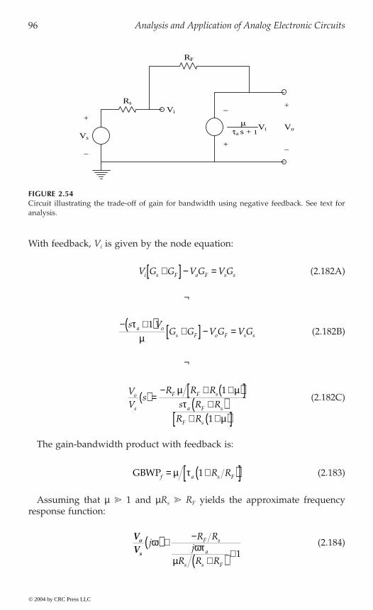
96 Analysis and Application of Analog Electronic Circuits
With feedback, Vi is given by the node equation:
(2.182A)
Ø
(2.182B)
Ø
(2.182C)
The gain-bandwidth product with feedback is:
(2.183)
Assuming that m 1 and mRs RF yields the approximate frequencyresponse function:
(2.184)
FIGURE 2.54Circuit illustrating the trade-off of gain for bandwidth using negative feedback. See text foranalysis.
τa s + 1
+
−
µ Vi
Vi
RF
Rs
Vs
+
− −
+
Vo
V G G V G V Gi s F o F s s+[ ] - =
- +( ) +[ ] - =s V
G G V G V Ga os F o F s s
tm
1
VV
sR R R
s R R
R R
o
s
F F s
a F s
F s
( ) =- + +( )[ ]
+( )+ +( )[ ]
m mt
m
1
1
GBWPf a s FR R= +( )[ ]m t 1
VV
o
s
jR R
jR R R
F s
a
s s F
w wtm
( ) @-
+( ) + 1
© 2004 by CRC Press LLC

Models for Semiconductor Devices Used in Analog Electronic Systems 97
Note the trade-off between closed-loop gain and bandwidth; the lower themid-band gain magnitude is, -RF/Rs, the higher the break frequency,
The choice of transistor for a high-frequency amplifier design is para-mount. BJTs must be chosen to have high fT s, and FETs to have high fmax.Although it may never be necessary to design a discrete or an IC multistageamplifier, the factors described earlier that go into the design of broadbandamplifiers should appreciated.
2.6 Photons, Photodiodes, Photoconductors, LEDs, and Laser Diodes
2.6.1 Introduction
This section examines the properties of semiconductor devices that sensephoton energy and others that emit photon energy. Photons are an alternateway to describe electromagnetic (EM) radiation generally having wave-lengths from 1 ¥ 10-4 m to less than 3 ¥ 10-12 m. These wavelengths includeinfrared (IR); visible light; ultraviolet (UV); x-rays; and gamma rays. Thephoton is a quantum EM “particle” used to describe physical interactions oflow-power EMR with molecules, atoms, and subatomic particles, such asatomic shell electrons. The electromagnetic wave characterization of EMenergy is used throughout the EM spectrum and finds application in describ-ing the operation of antennas, transmission lines, fiber optic cables, andoptical elements such as lenses, prisms, and mirrors used in IR, visible, andUV wavelengths. Maxwell’s equations for EM wave propagation are alsouseful in describing such phenomena as diffraction, refraction, and polar-ization of light (Balanis, 1989; Hecht, 1987).
A photon has essentially zero mass; it moves at the speed of light in amedium and has an individual energy of e = hc/l = hn joules, where h isPlanck’s constant (6.6253 ¥ 10-34 joule-second); c is the speed of light in thesupporting medium (c = 2.998 ¥ 108 m/sec in vacuo); l is the wavelength ofthe EM radiation in meters; and n is the Hertz frequency of the EMR (n ofvisible light is approximately 1014 Hz). Photon energy is also given in elec-tronvolts (eV). To obtain the energy of a photon in eV, divide its energy injoules by 1.602 ¥ 10-19. (1.602 ¥ 10-19 is the magnitude of the charge on anelectron.) For example, a photon of blue light with a wavelength of l =450 nm has an energy of e = (6.626 ¥ 10-34 J s)(3 ¥ 108 m/s)/(450 ¥ 10-9 m) =4.41 ¥ 10-19 J or 2.76 eV. Similarly, a photon of l = 700 nm (red light) has anenergy of 2.84 ¥ 10-19
wm
tbs s F
a
R R Rr s=
+( )
© 2004 by CRC Press LLC
J or 1.77 eV. Figure 2.55 illustrates the EM spectrum.
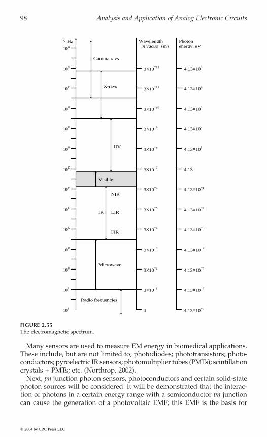
98 Analysis and Application of Analog Electronic Circuits
Many sensors are used to measure EM energy in biomedical applications.These include, but are not limited to, photodiodes; phototransistors; photo-conductors; pyroelectric IR sensors; photomultiplier tubes (PMTs); scintillationcrystals + PMTs; etc. (Northrop, 2002).
Next, pn junction photon sensors, photoconductors and certain solid-statephoton sources will be considered. It will be demonstrated that the interac-tion of photons in a certain energy range with a semiconductor pn junctioncan cause the generation of a photovoltaic EMF; this EMF is the basis for
FIGURE 2.55The electromagnetic spectrum.
© 2004 by CRC Press LLC
1015
1014
1011
109
ν Hz
1020
X-rays
UV1016
NIR
FIR
Microwave
108
Wavelength Photonenergy, eV
Visible
3X10⁻³
3X10⁻²
3X10⁻⁴
10133X10
−5
3X10⁻⁶
LIR
3X10⁻⁷
3X10⁻⁸
3X10⁻⁹
3X10⁻¹⁰
3X10⁻¹¹
3X10⁻¹²
3X10⁻¹
3
4.13X10⁵
1019 4.13X10⁴
1018 4.13X10³
1017 4.13X10²
4.13X101
4.13
IR
4.13X10⁻¹
4.13X10⁻²
10124.13X10
−3
4.13X10⁻⁴
10104.13X10
−5
Radio frequencies
4.13X10⁻⁶
4.13X10⁻⁷
1021 in vacuo
Gamma rays
(m)
Models for Semiconductor Devices Used in Analog Electronic Systems 99
photodiode behavior and the solar cell as an energy transducer (photons toelectrical current flow) capable of doing work. Photodiodes and solar cellscan be used to measure incident EM radiation intensity. Also treated in thefollowing sections are the generation of photon energy by special semicon-ductor diode structures, the light-emitting diode (LED) and the laser diode.Both types of photon-emissive devices have found wide application in bio-medical instrumentation (Northrop, 2002).
2.6.2 PIN Photodiodes
Photodiodes are used as sensors for EMR ranging from near infrared (NIR)to near ultraviolet (UVA). Even a standard small-signal silicon pn junctiondiode with a transparent glass envelope will respond to incident EMR ofappropriate wavelength, as will a reverse-biased LED. However, photo-diodes used for photonic measurements have specialized junction structuresthat maximize the area over which incident photons are absorbed. Photo-diodes are used in a broad range of biomedical instruments, including bloodpulse oximeters; finger-tip heart-rate sensors; single-drop blood glucosemeters; fiber-optic-based spectrophotometers (used to sense analytes in blood,urine, etc.); spectrophotometric detection of tumors using endoscopes; etc.
Photodiodes fall into two broad categories: (1) three-layer, PIN diodes (“I”stands for intrinsic semiconductor) and (2) avalanche photodiodes (APDs),
matic cross sections through two types of PIN devices. Note that to improvethe efficiency of photon capture, a thin, l/4 layer of antireflective (AR)coating is used on the surface of the PD, similar to the AR coatings commonlyused on binocular and camera lenses. Assume an incident photon with theappropriate energy passes through the AR coating, enters the P+ diffusionlayer, and interacts (collides) with a valence-band electron. If the electrongains energy greater than the band-gap energy, Eg, it is pulled up into theconduction band, leaving a hole in the valence band.
These electron–hole pairs are formed throughout the P+ layer, the deple-tion layer, and the N-layer materials. In the depletion layer, the E-fieldaccelerates these photoelectrons toward the N-layer and the holes towardthe P-layer. Electrons from the electron–hole pairs generated by photons inthe N-layer, along with electrons that have arrived from the P-layer, are leftin the N-layer conduction band. Meanwhile the holes diffuse through theN-layer up to the depletion layer while being accelerated and are collectedin the P-layer valence band. By these mechanisms, electron–hole pairs, whichare generated in proportion to the amount of incident light, are collected inthe N- and P-layers of the PD. This results in a positive charge in the P-layerand a negative charge in the N-layer.
When an external circuit is connected between the P- and N-layers, photo-current electrons will flow away from the N-layer and holes will flow awayfrom the P-layer, toward the opposite electrode. The PIN PD and the external
© 2004 by CRC Press LLC
which are basically four-layer structures (P+IPN). Figure 2.56 illustrates sche-
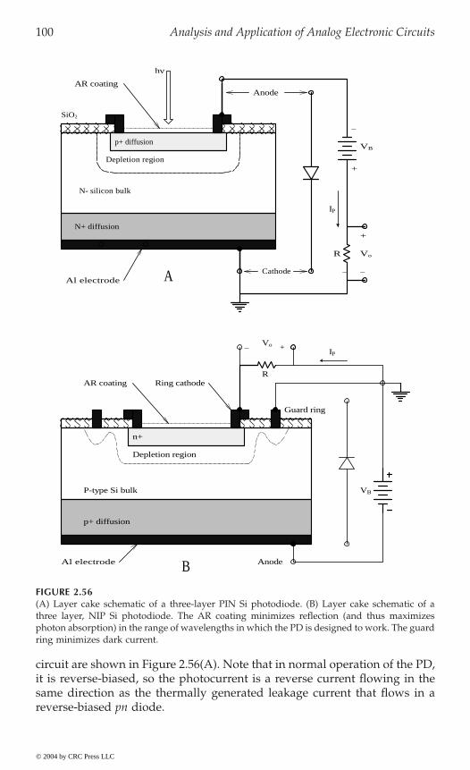
100 Analysis and Application of Analog Electronic Circuits
circuit are shown in Figure 2.56(A). Note that in normal operation of the PD,it is reverse-biased, so the photocurrent is a reverse current flowing in thesame direction as the thermally generated leakage current that flows in areverse-biased pn diode.
FIGURE 2.56(A) Layer cake schematic of a three-layer PIN Si photodiode. (B) Layer cake schematic of athree layer, NIP Si photodiode. The AR coating minimizes reflection (and thus maximizesphoton absorption) in the range of wavelengths in which the PD is designed to work. The guardring minimizes dark current.
AnodeAR coating
−
SiO2
Al electrodeCathode
N- silicon bulk
N+ diffusion
p+ diffusion
Depletion region+
VB
−
+
R Vo
Al electrode Anode
AR coating
Guard ring
Ring cathode
Vo +−
R
n+
Depletion region
P-type Si bulk
p+ diffusion
VB
IP
IP
AR coatingAnode
hν
A
B
−
© 2004 by CRC Press LLC

Models for Semiconductor Devices Used in Analog Electronic Systems 101
Figure 2.57 illustrates typical PIN PD volt–ampere curves. The load linerepresents a graphical solution of the PD’s (nonlinear) volt–ampere curveswith the (linear) Thevenin circuit “seen” by the PD. The zero-current inter-cept of the load line on the VD axis is at -Thevenin open-circuit voltage; thezero-voltage intercept is -Thevenin short-circuit current. The load line per-mits a graphical solution of:
(2.185A)
or
vD = VB - iD R, (VB < 0 in reverse-biased diode.) (2.185B)
The slope of the load line is easily seen to be -1/R and depends only onthe Thevenin model parameters. Most PDs are operated in the third quad-rant, either with a reverse-bias OCV or under short-circuit conditions (vD =0). PD signal-conditioning circuits will be described later.
FIGURE 2.57Top: simple series circuit for PIN PD. Bottom: iD vs. vD curves as a function of absorbed photonpower, Pi. The load line is determined by the Thevenin equivalent circuit that the PD “sees.”Note that the PD’s photocurrent, IP, flows in the reverse direction. Vo across the load resistorcan be determined graphically by the intersection of the iD = f(Pi) line with the load line.
vD
IP
Load-line
−VB /R
VB
R IPVo = IPR
+
Ip ≅ q η (Pi λ/hc)
(Pi in watts)
vD
+
−
−VB
intensityIncreasing light
hη
iDiD
Vo
Pi = 0(dark)
i vV v
RD DB D( ) = -
© 2004 by CRC Press LLC
102 Analysis and Application of Analog Electronic Circuits
The total PD current can be modeled by:
(2.186)
where the photocurrent, IP, flows in the reverse direction and is given by:
(2.187)
where Pi is the total photon power incident on the PD active surface in watts;VT = kT/q, h is the capture efficiency (approximately 0.8); and Irs is the reversesaturation current. Irs is very temperature dependent; it can be approximatedby (Navon, 1975; Millman, 1979):
or
(2.188B)
where T is the Kelvin temperature; To is the Kelvin reference temperature; fis the silicon energy gap (1.15 eV); and k is Boltzmann’s constant (1.380 ¥10-23 J/K). The simple PD model given by Equation 2.186 does not includethe ohmic leakage of the reverse-biased PD. Such leakage can be an appreciableportion of the reverse dark iD for large reverse vD.
If the PIN PD is operated at zero iD, photon power produces an open-circuit voltage given by:
(2.189)
Silicon PIN PDs are useful over a wavelength band covering approxi-mately 200 to 1100 nm; their spectral sensitivity rises slowly to a peak atapproximately 800 nm, then falls off rapidly. Sensitivity is given by the PD’sresponsivity in amps per watt; R(l) = iD(0)/Pi. R(l) peaks at approximately
PD responsivity plot. PDs can also be fabricated using germanium (Ge) andInGaAs. The former material responds from approximately 300 to 1600 nmand the latter composition has a spectral responsivity range from approxi-mately 800 to 2600 nm. Depending on operating conditions, PIN PDs areuseful over a range of picowatts to milliwatts of optical power.
i I v V ID rs D T P= ( ) -[ ] -exp 1
Iq PhcP
i= h l amperes
I T I Trs rs oT To( ) = ( ) -( )2 10
DI I T kTrs rs = + ( )[ ] @ ∞12
23 0 08f . K
v kT qq Phc IDoc
i
rs
= ( ) +È
ÎÍ
˘
˚˙ln 1
h l open-circuit volts
© 2004 by CRC Press LLC
0.55 A/W at approximately 850 nm. Figure 2.58 shows a “typical” Si PIN
Models for Semiconductor Devices Used in Analog Electronic Systems 103
Figures of merit for PDs include the responsivity R(l), described previ-ously; the noise-equivalent (optical) power (NEP); and the detectivity (D*).The NEP is the incident Pi at l required to generate a short-circuit responsecurrent, IP, equal to the RMS noise current of the detector system (unityoutput signal-to-noise ratio.) NEP is a measure of the minimum detectablenoise power at a given wavelength and bandwidth. In other words,
(2.190)
The noise generated by a PD operating under reverse bias is due to shotnoise generated in the dark leakage current and Johnson (thermal) noisegenerated in the equivalent shunt resistance of the PD. Shot and thermalnoises are broadband and considered to have flat white power density spec-
by:
(2.191)
where q is the magnitude of the electron charge; IDL is the dark leakagecurrent in amperes (IDL is zero for a zero-biased PD); and B is the equivalent
FIGURE 2.58A typical responsivity plot for a Si PIN PD. See text for discussion.
λ, nm
200 400 600 800 1000 1200
0.7
0.6
0.5
0.4
0.3
0.2
0.1
0.0
R(λ) (A/ W)
NEPrms noise currentresponsivity @
Wattsll
( ) =
i q I Bsn DL2 2= msA
© 2004 by CRC Press LLC
tra (See Chapter 9). The mean-squared shot noise can be shown to be given

104 Analysis and Application of Analog Electronic Circuits
Hertz noise bandwidth over which the noise current is measured. The mean-squared thermal noise can be shown to be given by:
(2.192)
where k = Boltzmann’s constant (1.38 ¥ 10-38 J/K); T = Kelvin temperatureof PD; B = equivalent Hertz noise bandwidth; and G = net thermal noiseproducing resistance. The total MS diode noise current is found by addingthe two MS current noises:
(2.193)
Thus the total RMS diode noise is:
(2.194)
Johnson noise dominates as the dark current Æ 0. Note that NEP dependson l, IDL (thus the PD operating circuit), the noise bandwidth B, T, and thenet (Norton) conductance, G, in parallel with the photocurrent and noisecurrent sources. The NEP for Si PIN PDs ranges from approximately10–14 W/ for small-area (A = 1 mm2) low-noise PDs, to over 2 ¥10–13 W/ for very large area cells (A = 100 mm2). Obviously, the NEP isdesired to be as small as possible. Note that manufacturers give NEP inde-pendent of the noise Hertz bandwidth, B. NEP must be multiplied by the
to get the actual NEP in watts.Often the input light power, Pi, is chopped; that is, the beam is periodically
interrupted by a chopper wheel, effectively modulating the beam by multi-plying it by a 0,1 square wave. The chopping rate is generally at audiofrequencies (e.g., 1 kHz) and the bandwidth of the associated band-pass filterused to condition the PD output determines B. Chopping is used to avoidthe excess 1/f diode noise present at DC and very low frequencies.
showing signal, noise, and dark current sources, the diode small-signalcapacitance, Cd, which is a depletion capacitance that depends on -vDQ, anddiode semiconductor doping and geometry. Note that the DC reverse leakagecurrent has two components: a constant small Irs and a voltage-dependentdark current, IDL. (IDL + Irs) are used to calculate isn. Normally, RL R, so thethermal noise current is found using the external load resistor, R (1/R = G).The junction depletion capacitance, Cd, decreases as vDQ goes more negative.Large Cd is deleterious to PD high-frequency response because it shunts IP(jw)to ground. Note that Cd increases with illumination and is smallest in the dark
d
one Si PIN PD with 1 mm2 active area and a vDQ = -10 V has a Cd @ 4 pF.
i k T GBtn2 4= msA
i i in sn tn2 2 2= + msA
i i q I k T G Bn n DL= = +( )2 2 4 rmsA
HzHz
B
© 2004 by CRC Press LLC
Figure 2.59 illustrates the equivalent model for a reverse-biased Si PIN PD,
(using the circuit of Figure 2.57). C is on the order of picofarads. For example,
Models for Semiconductor Devices Used in Analog Electronic Systems 105
D* is 1/NEP for the detector element only, normalized to a 1 cm2 activearea. D* is used only for comparisons between PDs of different active areas.D* units are cm /W. (A “better” PD has a higher D*.)
2.6.3 Avalanche Photodiodes
depending on diode design. The internal E-field completely depletes thep-region of mobile carriers. The E-field in the p-region causes any injectedor thermally generated carriers to attain a saturation velocity, giving themenough kinetic energy so that their impact with valence-band electronscauses ionization — the creation of other electron–hole pairs — that in turnare accelerated by the E-field, causing still more impact ionizations, etc.
Photon-generated electron–hole pairs are separated by the E-field in thep- and p-regions; electrons move into the n+ layer and holes drift into thep+ layer, both of which are boundaries of the APD’s space-charge region.These photon-generated carriers are multiplied as they pass through theavalanche region by the impact ionization process. At a given reverse oper-ating voltage, -vDQ = VR, one electron generated by photon collision producesM electrons at the APD’s anode. The contribution of electrons to IP is muchgreater than that from holes because electrons generated in the p- andp-regions are pulled into the avalanche region, whereas holes are swept backinto the p+ region (including the holes generated in the avalanche process).
APD noise is due to shot noise. As in the case of the PIN PD, the shotnoise is a broadband (white) Gaussian noise whose mean-squared value isproportional to the net DC component of the APD’s anode current, IDtot. TheDC anode current has two components; dark leakage current, IL, and DCphotocurrent, IP. The mean-squared shot noise current is given by:
(2.195)
FIGURE 2.59Model for a reverse-biased Si PIN photodiode. isn is the DC current-dependent shot noise rootpower spectrum; itn is the thermal noise root power spectrum. VB and R are components of theDC Thevenin circuit biasing the PD.
IDL
Cd
R
isn GL VB
RL >> R
IrsitnIP
Pi
−iD
iD
Vo +−
vD
+
Hz
i qB In Dtot2 2= msV
© 2004 by CRC Press LLC
A cross-sectional schematic of an avalanche PD (APD) is shown in Figure2.60. In an APD, a large reverse-biasing voltage is used, about 100 V or more,

106 Analysis and Application of Analog Electronic Circuits
It is clear that the lowest APD shot noise occurs when the ADP is operated
RMS shot noise current as a function of the DC reverse-bias voltage on a“typical” Si APD. The total leakage current, IL, can be written as:
IL = ILS + M ILB (2.196)
where ILS is the surface leakage current (not amplified) and ILB is the bulkleakage current (amplified by the avalanche process). The theoretical MSshot noise current may also be written (Perkin-Elmer, 2003):
(2.197)
where q is the electron charge magnitude; ILS is the dark surface leakagecurrent; ILB is the dark bulk leakage current; IP = Pi R1(l) M is the amplifiedDC photocurrent; and F is the excess noise factor. In general, F = rM + (1 - r)(2 - 1/M). Because M ª 100, F @ 2 + rM. The parameter, r, is the ratio ofhole to-electron ionization probabilities and is <1. M is the voltage-depen-dent APD internal gain. It is defined as the ratio of the output current at agiven Pi, l, and DC reverse-bias voltage, VR, to the output current for the
FIGURE 2.60Cross-sectional layer cake model of an avalanche photodiode.
i qB I I M PR M Fn LS LB i2 2
12= + + ( )[ ] l msA
© 2004 by CRC Press LLC
at very low (average) light levels. Figure 2.61 illustrates the peak gain and
AR coating
p+
Backsidemetallization
hν
Equivalentdiode
Anode
Cathode
Cathode metalring
n+
p
π region
iD
VB
R
iD
IP
Pi
n n
Models for Semiconductor Devices Used in Analog Electronic Systems 107
same input (Pi and l), but at a low dc reverse-bias voltage, say 10 V. Pi isthe incident optical power at wavelength l, R(l,VD) is the spectral respon-sivity in A/W, and B is the Hertz noise bandwidth.
The PE C30902S APD has the following parameters at a reverse voltage ofapproximately 225 V: F = 0.02M + 0.98(2 - 1/M). M = 250 at 830 nm; thus,F = 6.956. The responsivity at 830 nm is R(l) = 128 A/W. (Dividing theresponsivity at 830 nm by M yields R1(830) = 0.512 A/W.) Total dark currentis ID = 1 ¥ 10-8 A. The noise current root spectrum is in = 1.1 ¥ 10-13
RMSA/ . The shunt capacitance is Cd = 1.6 pF. The rise time and fall timeto an 830-nm light pulse with a 50 W RL (10 to 90%) is tr = tf = 0.5 ns.
The wavelength range of the APD responsivity curve, R(l), depends onAPD material; Si APDs are useful between 300 to 1100 nm, Ge APDs between800 and 1600 nm, and InGaAs devices between 900 to 1700 nm. The peakresponsivity depends on the average reverse-bias voltage on the APD. R1(l)is defined as the APD’s responsivity at a low VR such that M = 1. Thus, theAPD’s (amplified) photocurrent can be written
IP = Pi R1(l) M = Pi R(l) amps (2.198)
FIGURE 2.61Plot of peak photonic gain, M, and shot noise root power spectrum, in, for a typical avalanche PD.
180 2000 20 40 60 80 100 120 140 160
1.0
0.1
10
100
103
Gain (M) or Noise Current (pA/√Hz)
2.0
20
200
0.2
M
in
Reverse Bias Voltage, V.
Hz
© 2004 by CRC Press LLC

108 Analysis and Application of Analog Electronic Circuits
at a given l and VR, as shown in Equation 2.195. As noted earlier, the totalshot noise from an APD depends not only on dc leakage current, but alsoon dc photocurrent. There is also a noise current from any Thevenin con-ductance shunting the APD. Thus, the total diode noise in MSA is given by:
(2.199)
The APD’s MSSNR can be written, noting that F @ 2 + rM:
(2.200)
Inspection of the denominator of the right-hand SNR expression showsthat it has a minimum at some M = Mo, which results in a maximum SNR,other factors remaining constant. This optimum Mo is illustrated in Figure2.62. Recall that M is set by the DC reverse bias on the APD, VR, so findingthe optimum VR and M to optimize the APD SNR can be arty.
2.6.4 Signal Conditioning Circuits for Photodiodes
The most basic signal conditioning circuit for a PD is the simple DC Thevenin
FIGURE 2.62Plot of signal current and RMS shot noise current for a typical APD vs. gain M, showing theoptimum M where the diode’s RMS SNR is maximum.
signal current,rmsA
Mopt1
rmsA
10 100 103
Gain M
thermal noisecurrent
_______√4kTGLB
rms shotnoise current
max SNR
IP = Pi R1(λ)M
_________________√2qB(Pi R1(λ)MF + IL)
i qB I I M P R M F k T G Bn LS LB i L2 2
12 4= + + ( )[ ] +l msA
SNR = ( )+ + ( )[ ] +
= ( )+ + ( )[ ] +( ) +
P R M
qB I I M PR MF k T G B
P R B
q I M I PR M M k T G M
i
LS LB i L
i
LS LB i L
212 2
1
212
21
2
2 4
2 2 4
ll
ll r
© 2004 by CRC Press LLC
circuit shown in Figure 2.57. As discussed in the text, the output voltage

Models for Semiconductor Devices Used in Analog Electronic Systems 109
from the photocurrent can be found graphically using the load line deter-mined by VB and R. Neglecting dark current, it is simply:
Vo = qh(Pi l/hc)R volts (2.201)
An active circuit commonly used to condition PD output is shown inFigure 2.63. Because the summing junction of the op amp is at virtual ground,the PD is held at a constant reverse bias, VB. IP flows through RF, so Ohm’slaw tells that Vo = qh(Pi l/hc) RF, neglecting leakage (dark) current. Byoperating a PIN PD at reverse bias, the junction depletion capacitance, Cd,is made smaller and the diode’s bandwidth is increased. Unfortunately,reverse bias also increases the leakage current and thus the device’s shotnoise. If VB is made zero, then Cd is maximum and the PD’s bandwidth islowest. At zero bias, the leakage current Æ 0 and the diode’s shot noise is
F
and the op amp contribute noise to Vo; this noise will not be discussed here,however.
FIGURE 2.63Top: op amp signal conditioning circuit for a PIN PD operated at constant bias voltage. Bottom:plot of PD iD vs. vD curves showing the constant voltage load line.
vD
−VB /R
intensityIncreasing light
iD
IP = qη(Pi λ /hc)
(dark)Pi = 0
−VB
Pi
hν IP
+VB
Vo
RFPD
IOA
Load-line
(0)
© 2004 by CRC Press LLC
minimal, depending only on the photocurrent. As Chapter 9 will show, R
110 Analysis and Application of Analog Electronic Circuits
Sometimes a resistor is added in series with VB to limit the current throughthe PD. This circuit is shown in Figure 2.64. Note that the maximum PDcurrent is determined by the load line and is iD = -VB/R. APDs are run withthe same circuit, except VB is on the order of hundreds of volts and the seriesR (typically ≥1 MW) serves to protect the APD from excess reverse currentthat, for most APDs, is on the order of hundreds of microamperes. Althoughthe series resistor protects the ADP from excess reverse current, it also pro-duces thermal (Johnson) noise over and above the APD’s shot noise, as wellas the noise produced in the op amp circuit
An op amp circuit can be used to condition the output of a PIN PD toi
PD is operated in the zero current mode. Solving for vDoc:
FIGURE 2.64Top: op amp signal conditioning circuit for a PIN PD biased from a Thevenin dc source. Bottom:plot of PD iD vs. vD curves showing the load line.
vD
intensityIncreasing light
iD
(dark)Pi = 0
Pi
Vo
RFPD
IOA
Load-line
(0)
VB
+
−VB
VB /R
hν
IP R
IP = qη(Pi λ /hc)
© 2004 by CRC Press LLC
yield a logarithmic output proportional to P , as shown in Figure 2.65. The
−
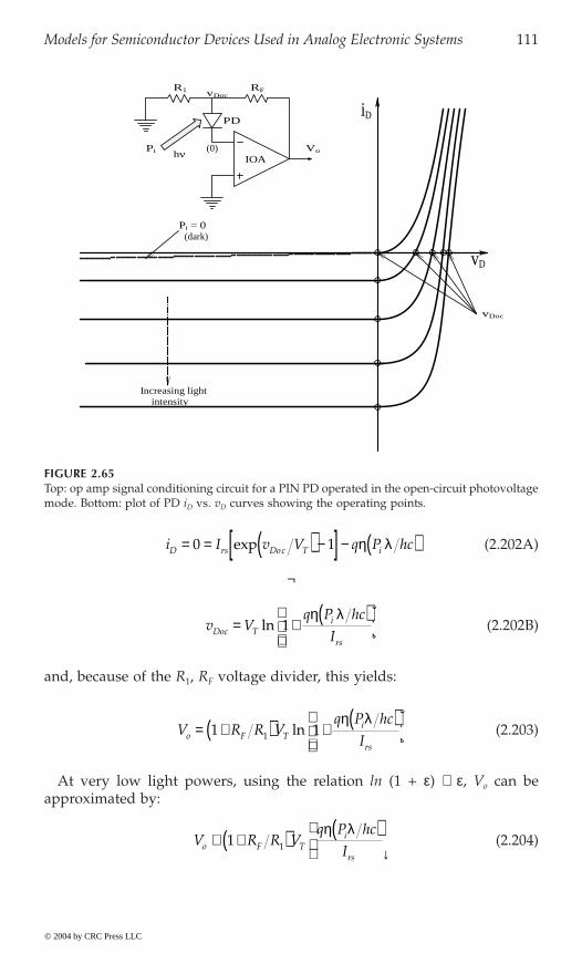
Models for Semiconductor Devices Used in Analog Electronic Systems 111
(2.202A)
Ø
(2.202B)
and, because of the R1, RF voltage divider, this yields:
(2.203)
At very low light powers, using the relation ln (1 + e) @ e, Vo can beapproximated by:
(2.204)
FIGURE 2.65Top: op amp signal conditioning circuit for a PIN PD operated in the open-circuit photovoltagemode. Bottom: plot of PD iD vs. vD curves showing the operating points.
vD
intensityIncreasing light
iD
(dark)Pi = 0
Vo
IOA(0)
PD
RFvDocR1
Pi hν
vDoc
i I v V q P hcD rs Doc T i= = ( ) -[ ] - ( )0 1exp h l
v Vq P hc
IDoc Ti
rs
= + ( )È
ÎÍÍ
˘
˚˙˙
ln 1h l
V R R Vq P hc
Io F Ti
rs
= +( ) + ( )È
ÎÍÍ
˘
˚˙˙
1 11 lnh l
V R R Vq P hc
Io F Ti
rs
@ +( ) ( )Ê
ËÁˆ
¯1 1
h l
© 2004 by CRC Press LLC

112 Analysis and Application of Analog Electronic Circuits
Typical parameter values are (1 + RF/R1) = 103, VT = kT/q = 0.0258, q =1.602 ¥ 10-19 Cb, h @ 0.8, l = 512 nm, h = 6.625 ¥ 10-34 J.sec, c = 3 ¥ 108 m/s,Irs @ 1 nA, and NEP @ 5 ¥ 10-14 W. Neglecting leakage (dark) current, Vo canbe calculated for Pi = 1 pW at l = 512 nm: \Vo = 8.51 mV.
Several manufacturers make ICs containing a PIN photodiode with an on-chip amplifier e.g., Burr–Brown makes the OPT202. This photosensor has a2.29 ¥ 2.29 mm PD coupled to an op amp with an internal 1-MW feedbackresistor, as shown in Figure 2.66. This IC works over a wide supply voltagerange (±2.25 to ±18 V) and has a voltage output responsivity of 0.45 V/mWat l = 650 nm with its internal RF = 1 MW. It has a -3-dB bandwidth of 50 kHzand a 10 to 90% rise time of 10 ms. To alter system responsivity, the RF canbe made larger or smaller than the internal 1 MW RF. The IC’s NEP is 10–11 Wfor B = 1 kHz and l = 650 nm with RF = 1 MW.
FIGURE 2.66Top: schematic of the Burr–Brown OPT202 IC photosensor. Bottom: spectral sensitivity of theOPT202 sensor. See text for details.
3 pF
175Ω
IP
V−V+
Vo
1MΩ RF 4
5
318
2 BB OPT202
PD
w/ internal1 MΩ RF
0.5
0.4
0.3
0.2
0.1
0
V/µW
Spectral Responsivity
200 400 600 800 1000λ (nm)
Pi
hν
© 2004 by CRC Press LLC
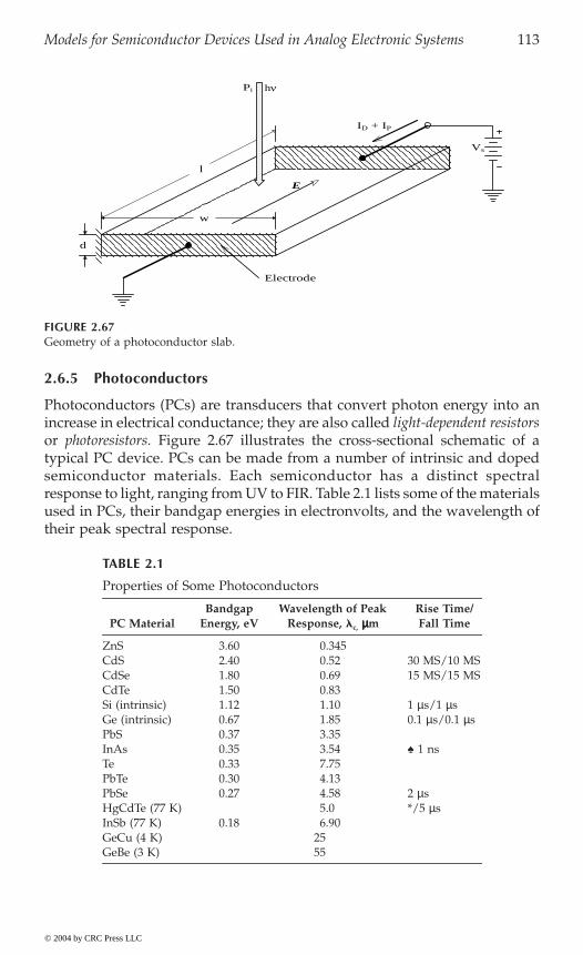
Models for Semiconductor Devices Used in Analog Electronic Systems 113
2.6.5 Photoconductors
Photoconductors (PCs) are transducers that convert photon energy into anincrease in electrical conductance; they are also called light-dependent resistorsor photoresistors. Figure 2.67 illustrates the cross-sectional schematic of atypical PC device. PCs can be made from a number of intrinsic and dopedsemiconductor materials. Each semiconductor has a distinct spectralresponse to light, ranging from UV to FIR. Table 2.1 lists some of the materialsused in PCs, their bandgap energies in electronvolts, and the wavelength oftheir peak spectral response.
FIGURE 2.67Geometry of a photoconductor slab.
TABLE 2.1
Properties of Some Photoconductors
PC MaterialBandgap
Energy, eVWavelength of Peak
Response, c, mmmmmRise Time/Fall Time
ZnS 3.60 0.345CdS 2.40 0.52 30 MS/10 MSCdSe 1.80 0.69 15 MS/15 MSCdTe 1.50 0.83Si (intrinsic) 1.12 1.10 1 ms/1 msGe (intrinsic) 0.67 1.85 0.1 ms/0.1 msPbS 0.37 3.35InAs 0.35 3.54 ª 1 nsTe 0.33 7.75PbTe 0.30 4.13PbSe 0.27 4.58 2 msHgCdTe (77 K) 5.0 */5 msInSb (77 K) 0.18 6.90GeCu (4 K) 25GeBe (3 K) 55
l
w
d
Vs
ID + IP
Pi hν
E
Electrode
© 2004 by CRC Press LLC
114 Analysis and Application of Analog Electronic Circuits
In general, the total current in a PC can be written:
IPC = Vs [GD + GP] (2.205)
where Vs is the bias voltage; GD is the equivalent dark conductance; and GP
is the photoconductance. GP can be shown to be given by (Yang, 1988):
(2.206)
where tp is the mean lifetime of holes; mp = vp/E = hole mobility incm2/V.sec; mn = vn/E = electron mobility in cm2/V.sec; vp and vn are themean drift velocities of holes and electrons, respectively; E is the uniformE-field in the semiconductor; and q, h, Pi, l, h, and c have been definedpreviously. Note that, in general, mn > mp. The expression for GP is an approx-imation, valid up to the cut-off wavelength, lc. [Pi l/hc] = Fi, the incomingnumber of photons/second on area wl m2. The dark conductance of a Si PCcan be found simply from the room temperature resistivity of Si, r, and thegeometry of the PC. For example:
(2.207)
From Equation 2.206, the photoconductance for a Si PC illuminated by1 mW of 512-nm photons is:
(2.208)
A great advantage of PCs is their unique ability to respond to MIR andFIR photons at wavelengths not sensed by PIN PDs or APDs. For variousmaterials, as the bandgap energy decreases, lc increases and the PC’sresponse time constants decrease.
PCs also are unique in their ability to convert x-ray photons to conductancechange. X-ray sensing PCs are made of amorphous selenium (a-Se) (Soltaniet al., 1999). An a-Se PC with E 10 V/mm produces approximately 1000electron–hole pairs per 50-keV x-ray photon. There is a 50% attenuation ofa 50-keV electron beam in d = 365 mm a-Se. Soltani et al. (1999) describe acharge-coupled x-ray photon-sensing array using a-Se sensors that havesuperior image resolution to phosphor x-ray sensors.
GIV
q
lPhcP
P
s
p p n i= =+( ) È
Î͢˚
h t m m l2 Siemens
G A l wd lD = = = ¥ ¥ ¥( )= ¥ -
r r 0 2
4 348 10 6
.
.
cm 0.001 cm 2.3 10 cm 0.02 cm
S
3 W
GP
Cb W mp
= ¥ ¥ ¥ ( ) ¥ ¥¥ ¥ ¥
È
Î
ÍÍÍ
˘
˚
˙˙˙
= ¥
- -
-
- -
-
-
1 6 10 0 8 1010
10 512 106 625 10 3 10
5 935 10
19 4
4
6 9
34 3
4
2
2
. ..
.
h t
1350 + 450
Siemens
cm V.sec
cm joule.sec m sec
© 2004 by CRC Press LLC

Models for Semiconductor Devices Used in Analog Electronic Systems 115
Figure 2.68 illustrates a simple op amp circuit that gives Vo µ Pi. Note thatRC is used to cancel the PC’s dark current. A Wheatstone bridge can also beused to convert photoconductance to output voltage, albeit nonlinearly.Unlike PDs, PCs make thermal noise; it can be shown that the total MS noisecurrent input to the op amp’s summing junction is:
(2.209)
Note that the MS noise increases with input light power because GP
increases with Pi. In addition to the noise current, the op amp also has anequivalent short-circuit input noise voltage, ena
2
sider such noise.
2.6.6 LEDs
Light-emitting diodes are widely used in all electronic applications as pilotlights, status indicators, and warning signals. They are also used in biomedicalapplications as (approximately) monochromatic light sources for chemicalanalysis by spectrophotometry. LEDs can be purchased that emit not onlynear IR, but also visible red, orange, yellow, green, blue, and white light. Animportant application for LEDs in biomedicine is the two light sources inthe pulse oximeter, which is basically a two-wavelength spectrophotometerused to measure blood oxygen saturation (Northrop, 2002). One NIR LEDemits at 805 nm, the isobestic wavelength for deoxyhemoglobin (Hb) andoxyhemoglobin (HbO2) absorbance (the wavelength at which Hb and HbO2
absorbances are equal). The other wavelength is at approximately 650 nm(red), where there is a large difference between the absorbances of Hb andHbO2. LEDs are also used as the light sources in the paper strip, bloodglucose sensing systems. Again, a two-l spectrophotometer is used. Eventhough LEDs are relative broadband emitters, their spectral purity is goodenough for simple spectrophotometric measurements.
FIGURE 2.68Op amp circuit for conditioning a photoconductive sensor’s output. The current through RC
compensates for the PC’s dark current.
RF
IP + ID PC
RC
+5 V
−15 VID
Vo = IP RF
Pi
IOA
(0)
i kT G G G G i Bntot D P C F na2 24= + + +[ ] + msA
© 2004 by CRC Press LLC
B MSV. Chapter 9 will con-

116 Analysis and Application of Analog Electronic Circuits
An LED is a solid-state, pn junction device that emits photons upon theapplication of a forward-biasing current. It converts electric energy directlyinto photon energy without the intermediate step of thermal conversion.LED p-material is typically doped gallium aluminum arsenide (GaAlAs),while the n-material is doped gallium arsenide (GaAs). Between the p andn layers is an active layer. When a forward voltage (and current) is appliedto the LED, holes from the p-region (GaAlAs) meet electrons from then-doped GaAs layer in the active layer and recombine, producing photons.Photon wavelength is dependent on the chemical composition and relativeenergy levels of the two doped semicon layers. It also depends to a smalldegree on the junction temperature and ID. Visible-light LEDs typically haveplastic dome lenses that serve to expand and diffuse the light from the LED’sactive layer. The plastic is colored to indicate the color of the emitted light;clear lenses are used for NIR LEDs.
The wavelength of the emitted light can be altered by varying the compo-sition of the doped semicon materials used in the LED. Typical materialsused in LED construction include Al, As, Ga, In, P, and N (as nitrides). Whitelight can be made by several mechanisms, but one way is to make a blueLED and use the blue light to excite a mixture of phosphors in the reflectorcup that emit at several longer wavelengths; the mixture of wavelengthsappears white.
LED forward voltage is on the order of 1.5 V and operating currents rangefrom a few to tens of milliamperes. When a forward current is appliedthrough a pn junction, carriers are injected across the junction to establishexcess carriers above the thermal equilibrium values. The excess carriersrecombine and, in so doing, some energy is released in the form of heat andlight (photons). The injected electrons in the p side make a downward energytransition from the conduction band to recombine with holes in the valenceband. Photons are emitted having energy, Eg, in joules. The emission wave-length is approximately:
l = hc/Eg meters (2.210)
In practice, the emission power spectrum is not a narrow band such asthat produced by lasers, but is a curve with a smooth peak and a Q definedby the wavelength of the peak emission power density divided by the Dlbetween the half-power wavelengths on either side of the peak. That is; Q =lpk/Dl. For example, Q @ 16 for a GaAsP LED with peak emission at 650 nm(Yang, 1988). The Qs for Osram LEDs LS5421, LO5411, LY5421, and LG5411 —emitting power peaks at 635, 610, 586 and 565 nm, respectively — are 14.1,15.3, 13.0, and 22.6, respectively.
Si pn junction diode, as shown on Figure 2.69(B). Figure 2.69(C) illustratesD
relative spectral emission of a GaP green LED. The peak is at approximately
© 2004 by CRC Press LLC
(GaP) LED. Compare this curve with the I–V curve for a typical small-signal,Figure 2.69(A) illustrates the I–V characteristics of a green gallium phosphide
the light intensity vs. I for the green LED and Figure 2.70 illustrates the
Models for Semiconductor Devices Used in Analog Electronic Systems 117
561 nm and the half-intensity width is measured at approximately 26 nm,giving an LED Q = 21.6.
Modern LEDs are now available in the near UV, which provides excellentapplication in biochemical fluorescence analysis as an inexpensive source ofexcitation for DNA microarrays (gene chips) and many other modes offluorescent chemical analysis. Their UV can also be used to catalyze thepolymerization of dental fillings and for spot sterilization. For example, theNichia NSHU550E UV LED (gallium indium nitride) has a spectral emissionpeak centered at 370 nm, quite invisible to the human eye. Nichia also makesgallium nitride (GaN) single quantum well LEDs that emit blue with a peakat approximately 470 nm that are intended for excitation in fluorescenceapplications, including protein analysis and DNA analysis using SYBR“green and SYPRO“ orange molecular tags.
The following section shows that laser diodes (LADs) have much narrowerspectral emission lines, but also can have under certain operating conditionsmany closely spaced emission lines.
2.6.7 Laser Diodes
The basic difference between an LED and an LAD is that the latter has anoptical resonance cavity that promotes lasing. The optical cavity has two endfacet partial mirrors that reflect photons back into the cavity so that a self-sustaining laser action occurs. The mirrors can be the cleaved surfaces of thesemiconductor crystals or may be optically ground, polished, and coated.The LAD unit generally contains a photodiode (PD) that is used with anexternal circuit to monitor the optical power output, Po, of the LAD. LADsare easily damaged by excess ID causing excess Po. Often the PD output isused to provide feedback to limit the optical power output of the LAD sothat the end mirrors are not damaged by heat or XS light. If the end mirrorsare damaged, the LAD becomes an expensive, ineffective LED.
TABLE 2.2
Semiconductor LED Materials and Approximate Emission Peak Wavelengthsa
Material Wavelength (mmmmm) Photon energy (eV)
GaP (Zn, diffused green) 0.553 2.24Ga1-x Alx As (red) 0.688 1.78GaP (Zn, 0-doped red) 0.698 1.76GaAs (NIR) 0.84 1.47InP 0.9 1.37Ga(Asx P1-x) 1.41–1.95GaSb 1.5 0.82PbS (MIR) 4.26 0.29InSb 5.2 0.23PbTe 6.5 0.19PbSe 8.5 0.145
a Peak emission, l, depends on temperature and diode current.
© 2004 by CRC Press LLC

118 Analysis and Application of Analog Electronic Circuits
Low-power LADs come in a variety of packages; probably the most famil-iar is the cylindrical can with top (end) window. Such TO-cans are typically5.6 or 9.0 mm in diameter and have three leads: (1) common, (2) LADcathode, and (3) PD anode. The PD’s cathode and the LAD’s anode areconnected to the common lead.
FIGURE 2.69(A) iD vs. vD curve for a GaP (green) LED. Note the high threshold voltage for forward conduc-tion. (B) For comparison, the iD vs. vD curve for a typical Si small-signal pn diode. (C) Relativelight intensity vs. forward current.
ID (mA)
25
20
15
10
5
0.5 1.0 1.5 2.0
VD
Irs
5
0.1
10
20
10.6 5 10 15 20 25
VD ID (mA)
A
B C 1.0
GaP (green) LED
GaP (green) LED
Si pn diode
Photonintensity
ID (mA) Relative
© 2004 by CRC Press LLC
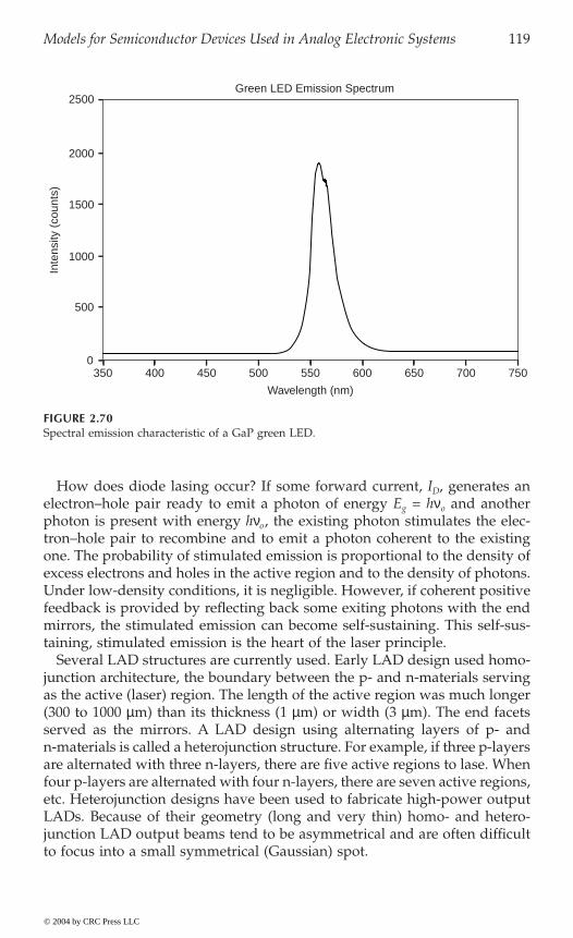
Models for Semiconductor Devices Used in Analog Electronic Systems 119
How does diode lasing occur? If some forward current, ID, generates anelectron–hole pair ready to emit a photon of energy Eg = hno and anotherphoton is present with energy hno, the existing photon stimulates the elec-tron–hole pair to recombine and to emit a photon coherent to the existingone. The probability of stimulated emission is proportional to the density ofexcess electrons and holes in the active region and to the density of photons.Under low-density conditions, it is negligible. However, if coherent positivefeedback is provided by reflecting back some exiting photons with the endmirrors, the stimulated emission can become self-sustaining. This self-sus-taining, stimulated emission is the heart of the laser principle.
Several LAD structures are currently used. Early LAD design used homo-junction architecture, the boundary between the p- and n-materials servingas the active (laser) region. The length of the active region was much longer(300 to 1000 mm) than its thickness (1 mm) or width (3 mm). The end facetsserved as the mirrors. A LAD design using alternating layers of p- andn-materials is called a heterojunction structure. For example, if three p-layersare alternated with three n-layers, there are five active regions to lase. Whenfour p-layers are alternated with four n-layers, there are seven active regions,etc. Heterojunction designs have been used to fabricate high-power outputLADs. Because of their geometry (long and very thin) homo- and hetero-junction LAD output beams tend to be asymmetrical and are often difficultto focus into a small symmetrical (Gaussian) spot.
FIGURE 2.70Spectral emission characteristic of a GaP green LED.
© 2004 by CRC Press LLC
Green LED Emission Spectrum
Wavelength (nm)
Inte
nsity
(co
unts
)
350 400 450 500 550 600 650 700 750
2500
1000
1500
2000
500
0

120 Analysis and Application of Analog Electronic Circuits
The new, vertical cavity, surface-emitting laser (VCSEL) diodes consist ofa (top) light exit window (it can be round, 5 to 25 mm in diameter), a top-distributed Bragg reflector, a gap to set the emission wave length, twol-spacers surrounding a GaAs active region, and then a bottom-distributedBragg reflector sitting on the bottom substrate. VCSEL lasers operate in asingle longitudinal mode. They can be designed to have anastigmatic Gaus-sian beams, which are easy to focus with simple lenses. Because the mirrorarea is larger, VCSEL lasers are not as prone to overpower damage andoptical feedback is not necessary as it is in edge-emitting LADs. They alsolase at much lower IDs because of their efficient mirrors.
LADs are considered to be current-operated devices; they should be driven
the optical output power, Po, from a LAD vs. the forward current, ID, for atypical heterojunction LAD. IDt is the threshold current where enough elec-tron–hole pairs are produced to sustain lasing. Note that increasing devicetemperature moves the Po(ID) curve to the right. The steep part of the curveis essentially linear and is characterized by its slope: DPo/DID = r watts/amp.In the region of ID between 0 and IDt, the LAD is basically a LED. An algebraicmodel for the Po(ID) curve above IDt is:
Po = rID - Px (2.211)
where Px is the intersection of the approximate line with the negative Po axis.Needless to say, IDt is much lower for a VCSEL LAD. (An Avalon, AVAP760,VCSEL, 760-nm LAD has IDt = 2.0 mA and IDQ = 3.0 mA. IDQ is the operatingcurrent for this LAD.)
Although VCSEL LADs have a single mode output (the preceding 760-nmVCSEL has a line Q of 3.95 ¥ 1014 Hz/100 ¥ 106 Hz = 3.95 ¥ 106), homo- andheterojunction LADs generally emit a multimode “comb” spectral output.The number of spectral lines that appear at the output of a gain-guided LADdepends on the properties of the cavity and mirrors, the operating current,and the temperature. According to the Newport Photonics Tutorial (2003):
The result is that multimode laser diodes exhibit spectral outputs havingmany peaks around their central wavelength. The optical wave propa-gating through the laser cavity forms a standing wave between the twomirror facets of the laser. The period of oscillation of this curve is deter-mined by the distance L between the two mirrors. This standing opticalwave resonates only when the cavity length L is an integer number mof half wavelengths existing between the two mirrors. In other words,there must exist a node at each end of the cavity. The only way this cantake place is for L to be exactly a whole number multiple of half wave-lengths l/2. This means that L = m(l/2), where l is the wavelength oflight in the semiconductor matter and is related to the wavelength oflight in free space through the index of refraction n by the relationshipl = lo/n. As a result of this situation there can exist many longitudinalmodes in the cavity of the laser diode, each resonating at its distinct
© 2004 by CRC Press LLC
from regulated current sources, not voltage sources. Figure 2.71(A) illustrates
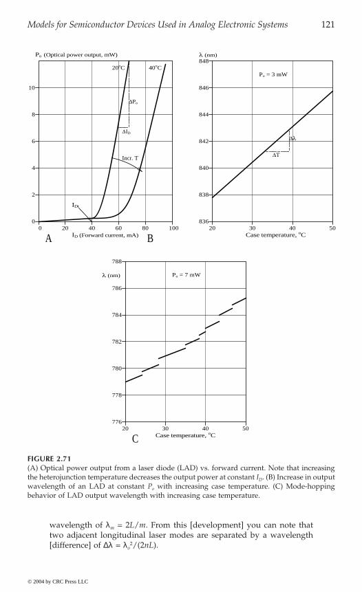
Models for Semiconductor Devices Used in Analog Electronic Systems 121
wavelength of lm = 2L/m. From this [development] you can note thattwo adjacent longitudinal laser modes are separated by a wavelength[difference] of Dl = lo
2/(2nL).
FIGURE 2.71(A) Optical power output from a laser diode (LAD) vs. forward current. Note that increasingthe heterojunction temperature decreases the output power at constant ID. (B) Increase in outputwavelength of an LAD at constant Po with increasing case temperature. (C) Mode-hoppingbehavior of LAD output wavelength with increasing case temperature.
20 30 40 50Case temperature, oC
776
778
780
782
784
786
788
λ (nm)
20 30 40 50836
838
840
842
844
846
848
Po = 3 mW
Po = 7 mW
Incr. T
∆Po
∆ID
40oC20oC
Po (Optical power output, mW)
20 40 60 800 1000
2
4
6
8
λ (nm)
10
∆T
∆λ
IDt
A BID (Forward current, mA) Case temperature, oC
C
© 2004 by CRC Press LLC
122 Analysis and Application of Analog Electronic Circuits
Even single-mode devices [VCSEL LADs] can support multiple [output]modes at low output power… As the operating current is increased, onemode begins to dominate until, beyond a certain operating power level,a single narrow linewidth [output] spectrum appears.
It is also noted that the center l of an LAD’s output increases with operatingtemperature. This property is useful in spectroscopy in which the fine struc-ture of a molecular absorbance spectrum is being studied. Newport givesdata for one LAD with a center frequency of 837.6 nm at 20∞C. The centerwavelength increases linearly with increasing temperature to 845.5 nm at50∞C. Thus, Dl/DT = 0.263 nm/∞C.
Single-mode LADs can exhibit a phenomenon known as mode-hopping.Here the output l increases linearly over a short temperature interval, at theupper end of which it hops discontinuously to a slightly larger l. The linearbehavior again occurs, followed by another hop, etc. The linear behavior of
Because of mode-hopping and l drift with temperature, LADs used for wavelength critical applications are temperature stabilized to approximately 0.1∞Caround a desired operating temperature using thermoelectric (Peltier) cooling.
Many circuits have been developed to drive LADs under constant-currentconditions. Some circuits use the signal from the built-in PD to stabilize thediode’s Po when CW or pulsed output is desired. In communications appli-cations, in which the LAD is driving an optical fiber cable, it is desirable toon/off modulate Po at very high rates, up into the gigahertz in some cases.In biomedical applications, in which the LAD is used as a source for spec-trophotometry, the intensity modulation or chopping of the beam is moreconveniently done at audio frequencies to permit the operation of lock-inamplifiers, etc.
One of the more prosaic applications of LADs is the common (CW) laserpointer. Some of these devices are operated without any regulation by thesimple expedient of using one current-limiting resistor in series with the twobatteries. The resistor is chosen so that ID is always less than IDmax when thebatteries are fresh. Of course the pointer spot gets dimmer as the batteries
solution of the LAD’s ID = f (VD) curve with the circuit’s load line.An example of a two-BJT regulator used in laser pointers (Goldwasser,
makes Po relatively independent of DVB and DT. Inspection of this circuitshows that if Po increases, the PD’s IP increases, decreasing IB2, thus IB1 andID, and thus reducing Po; therefore, negative feedback stabilizes Po.
When it is desired to modulate an LAD at hundreds of megahertz togigahertz for communications applications, very special circuits indeed areused. LADs can be modulated around some 50% Po point much faster thanfrom fully off to fully on. Several semiconductor circuit manufacturers offerhigh-frequency single-chip LAD regulator/drivers. For example, the Analog
© 2004 by CRC Press LLC
l(T) and mode-hopping are shown in Figure 2.71(B) and Figure 2.71(C).
become exhausted. Figure 2.72 illustrates this basic series circuit and the
2001) is shown in Figure 2.73. This is a type 0, negative feedback circuit that

Models for Semiconductor Devices Used in Analog Electronic Systems 123
FIGURE 2.72Top: LAD powered from a simple DC Thevenin circuit. Bottom: an LAD’s iD vs. vD curveshowing max iD, load lines, and operating point.
FIGURE 2.73A simple LAD Po (thus iD) regulator circuit. The LAD’s built-in PD is used to make a type 0intensity controller.
VD
VB − ∆V2 3
VB
VB /R
ID
0 1VDQ
IDQ
Max ID
VB
R
hνPoLAD
Load-line
LAD PD
IP
R1
R2
R3
R4
ID
Po Po
C
Q1
Q2IB1
VB
SW
IB2
© 2004 by CRC Press LLC

124 Analysis and Application of Analog Electronic Circuits
Devices AD9661A driver chip allows LAD on/off switching up to 100 MHz,and has <2 ns rise/fall times. The Maxim MAX3263 is a 155 Mbps LADdriver with <1 ns rise/fall times. Needless to say, getting an LAD to switchat such rates involves the artful use of ferrite beads, as well as considerationof parasitic distributed parameters such as LAD lead inductance and straycapacitances. The MAX3263 chip also has a “slow start” feature to protectthe LAD at turn-on. The design of GHz modulation circuits is beyond thescope of this text and will not be treated here.
Figure 2.74 illustrates the architecture of an op amp feedback/modulationcircuit designed by the author for spectrophotometric LAD applications. Ituses a VCCS to drive the LAD and a feedback loop containing signal con-ditioning for the on-board PD, a difference amplifier (DA), an integrator, andanother DA. The input that sets the LAD’s output power is VoQ, which canbe an audio-frequency square-wave, a sinewave + DC, or just DC. The VCCSsubunit drives the LAD. Its transconductance can be found by KVL, noting:
V2 = -(ID RF + VL) (2.212)
The node equation for the power op amp’s summing junction can bewritten:
(0)[2G + G1] - VcG1 - V2G - VLG = 0 (2.213)
FIGURE 2.74A type 1 feedback system designed by the author to regulate and modulate LAD Po. The LAD’sbuilt-in PD is used for feedback.
(VCCS)LAD PD
Po
VL
−VL
POA
RR
R
R
R R
V1 > 0 VoQ > 0
R
R R
RD
R
RR1
R VL
R (0)RF ID
Vo = kPo
Ve
Ve = (VoQ − Vo)
V3
C
Vc
−VL
(DA) (DA)(Integrator)
(PD amp)
V2
hν
© 2004 by CRC Press LLC
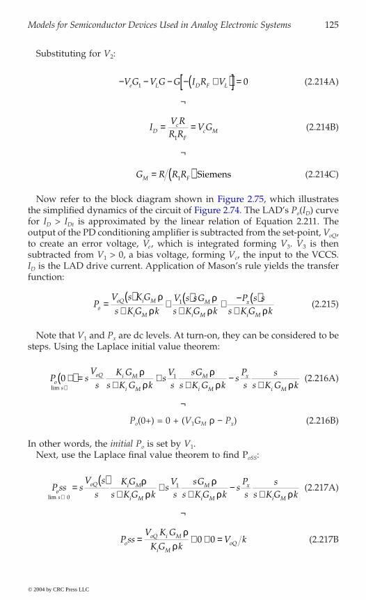
Models for Semiconductor Devices Used in Analog Electronic Systems 125
Substituting for V2:
(2.214A)
Ø
(2.214B)
Ø
(2.214C)
o D
for ID > IDt is approximated by the linear relation of Equation 2.211. Theoutput of the PD conditioning amplifier is subtracted from the set-point, VoQ,to create an error voltage, Ve, which is integrated forming V3. V3 is thensubtracted from V1 > 0, a bias voltage, forming Vc, the input to the VCCS.ID is the LAD drive current. Application of Mason’s rule yields the transferfunction:
(2.215)
Note that V1 and Px are dc levels. At turn-on, they can be considered to besteps. Using the Laplace initial value theorem:
(2.216A)
Ø
Po(0+) = 0 + (V1GM r - Px) (2.216B)
In other words, the initial Po is set by V1.Next, use the Laplace final value theorem to find PoSS:
(2.217A)
Ø
(2.217B
- - - - +( )[ ] =V G V G G I R Ve L D F L1 0
IV RR R
V GDc
Fc M= =
1
G R R RM F= ( )1 Siemens
PV s K G
s K G kV s sGs K G k
P s ss K G ko
oQ i M
i M
M
i M
x
i M
=( )
++ ( )
++
- ( )+
rr
rr r
1
P sV
sK G
s K G ks
Vs
sGs K G k
sPs
ss K G ko
s
oQ i M
i M
M
i M
x
i M
0 1+( ) =+
++
-+Æ •lim
rr
rr r
P ss sV s
sK G
s K G ks
Vs
sGs K G k
sPs
ss K G ko
s
oQ i M
i M
M
i M
x
i Mlim Æ=
( )+
++
-+0
1rr
rr r
P ssV K G
K G kV ko
oQ i M
i MoQ= + + =
rr
0 0
© 2004 by CRC Press LLC
Now refer to the block diagram shown in Figure 2.75, which illustratesthe simplified dynamics of the circuit of Figure 2.74. The LAD’s P (I ) curve
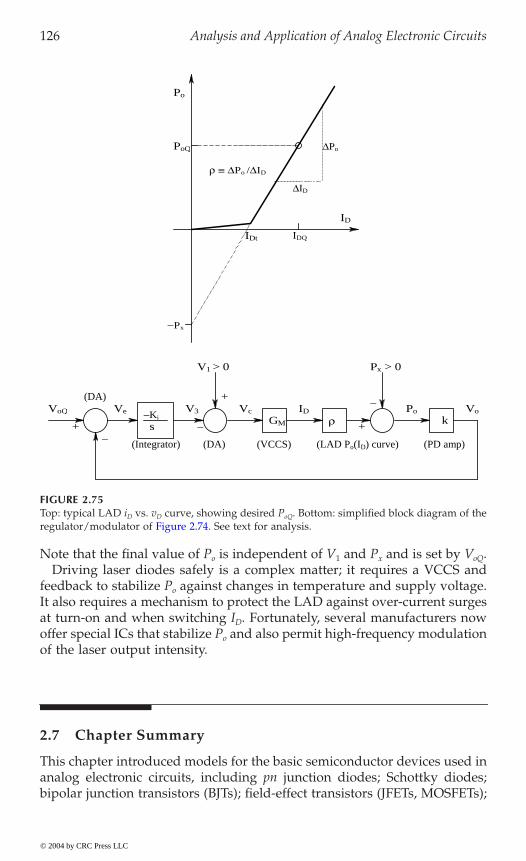
126 Analysis and Application of Analog Electronic Circuits
Note that the final value of Po is independent of V1 and Px and is set by VoQ.Driving laser diodes safely is a complex matter; it requires a VCCS and
feedback to stabilize Po against changes in temperature and supply voltage.It also requires a mechanism to protect the LAD against over-current surgesat turn-on and when switching ID. Fortunately, several manufacturers nowoffer special ICs that stabilize Po and also permit high-frequency modulationof the laser output intensity.
2.7 Chapter Summary
This chapter introduced models for the basic semiconductor devices used inanalog electronic circuits, including pn junction diodes; Schottky diodes;bipolar junction transistors (BJTs); field-effect transistors (JFETs, MOSFETs);
FIGURE 2.75Top: typical LAD iD vs. vD curve, showing desired PoQ. Bottom: simplified block diagram of the
V1 > 0
ID
Px > 0
Po
GM ρ kVoVcVe −Ki
V3
(DA)VoQ
−s+ −
−
+
+
(PD amp)(VCCS) (LAD Po(ID) curve)(Integrator) (DA)
ID
−Px
Po
IDt
∆Po
∆ID
IDQ
PoQ
ρ ≡ ∆Po /∆ID
© 2004 by CRC Press LLC
regulator/modulator of Figure 2.74. See text for analysis.

Models for Semiconductor Devices Used in Analog Electronic Systems 127
and some common solid-state photonic devices widely used in biomedicalinstrumentation, e.g., PIN photodiodes, avalanche photodiodes, LEDs, andlaser diodes.
The circuit element models were seen to be subdivided into DC-to-mid-frequency models and high-frequency models that included small-signalcapacitances resulting from charge depletion at reverse-biased pn junctions,and from stored charge in forward-conducting junctions. Mid-frequencymodels were used to examine the basic input resistance, voltage gain, andoutput resistance of simple, one-transistor BJT and FET amplifiers.
Also examined as analog IC “building blocks” were two-transistor ampli-fiers. High-frequency behavior of diodes, single-transistor amplifiers, andtwo-transistor amplifiers was examined. Certain two-transistor amplifierarchitectures such as the cascode and the emitter (source)-follower–grounded-base (gate) amplifier were shown to give excellent high-frequencyperformance because they minimized or avoided the Miller effect. Certainother broadbanding strategies were described.
Semiconductor photon sensors were introduced, including pin and ava-lanche photodiodes, and photoconductors. LEDs and laser diode photonsources were also covered, as well as circuits used in their operation.
Home Problems
2.1
a. Assume the diode is ideal. The voltage source is vs(t) = 10sin(377t) and the load is 10 W. Find the average power dissipatedin the load, RL.
b. Now let the diode be represented by the I–V curve in FigureP2.1B. Find the average power dissipated in the load and also inthe diode.
FIGURE P2.1
iD
iD
0.7 V
vD
0A
+ −vD
−
+
vD
RL
iD
vs
B
© 2004 by CRC Press LLC
A diode is used as a half-wave rectifier as shown in Figure P2.1A.
128 Analysis and Application of Analog Electronic Circuits
2.2 A diode bridge rectifier is shown in Figure P2.2. Each diode has the I–V curve
L
diode.
2.3 A zener diode power supply is shown in Figure P2.3. Its purpose is to deliver5.1 Vdc to an 85-W load, in which a 9-V battery is the primary dc source. A1N751 zener diode is used; its rated voltage is 5.1 V when a 20-mA reverse(zener) current, IZ, is flowing. Find the required value for Rs. Also find thepower dissipation in the diode, Rs and RL, and the power supplied by the
battery.
2.4 FE = 99, VBEQ = 0.65 V.
a. Find IBQ and RB required to make VEQ = 0 V.b. Calculate the quiescent power dissipation in the BJT and in RE.c. Calculate the small-signal hie for the BJT at its Q-point.
FIGURE P2.2
FIGURE P2.3
RL
vs
RL
Rs
Iz
1N751
5.1 V
Is
9.0 V
© 2004 by CRC Press LLC
of Figure P2.1B. Find the average power in the load, R , and also in each
Refer to the emitter follower in Figure P2.4. Given: h
Models for Semiconductor Devices Used in Analog Electronic Systems 129
2.5 A pnp BJT grounded-base amplifier is shown in Figure P2.5. Given: hFE =149, VBEQ = 0.65 V. Find RB and RC so that the amplifier’s Q-point is at ICQ =–1.0 mA, VCEQ = -5.0 V. Find VEQ.
2.6 FE = 100 (allthree BJTs), VCC = +6.0 V, R = 12 kW, VBE1 = 0.65 = VBE2, VBE3 = 0.60 V, VCE2
VCE2sat. Find (a) VCE1; (b) IR; (c) IE3; (d) IB3; and (e) IC1 and IC2.
2.7 BEQ =
0.65 V, hFE = 119. Find RB and RC so the Q-point is at ICQ = 2.5 mA, VCEQ = 7 V.
2.8 FE = 99, VBEQ =
–0.65 V.
a. Find RB and IBQ required to make VCEQ = -10 V.b. Find the quiescent power dissipated in the BJT and in RE.
FIGURE P2.4
FIGURE P2.5
−12 V
+12 V
RB
RE1.2 kΩ
VEQ ≡ 0
−12 V
RB
RE1 kΩ RC
VCQ
© 2004 by CRC Press LLC
The circuit shown in Figure P2.6 is a current mirror. Given: h
An npn BJT grounded base amplifier is shown in Figure P2.7. Given: V
A pnp BJT emitter follower is shown in Figure P2.8. Given: h

130 Analysis and Application of Analog Electronic Circuits
2.9amplifier, find the RB required to make ICQ = 1 mA. Also find VCEQ in each
circuit. Given: hFE = 100 and VBEQ = 0.65 V.
2.10amplifier is shown in Figure P2.10A. The source resistor, RS, is bypassed byCS, making the source node at small-signal ground. RS is required for self-biasof the JFET. The same JFET is used in all three circuits, in which IDSS =
FIGURE P2.6
FIGURE P2.7
IC2
IC1
+ 6 V
IE3
IR
Q2Q1
Q3
12 kΩ R
15 V
1.1 kΩ
RC
RB
2.5 mA
RE 7.0 V+−
© 2004 by CRC Press LLC
Consider the three basic BJT amplifiers shown in Figure P2.9. In each
Three JFET amplifiers are shown in Figure P2.10. A “grounded-source”

Models for Semiconductor Devices Used in Analog Electronic Systems 131
6.0 mA; VP = -3.0 V; and gmo = 4 ¥ 10-3
mQ, RS, and RD so that IDQ = 3.0 mA and VDQ = 8.0 V. Give VDSQ.Circuit (C) of Figure P2.10 is a source follower. Find R1 and RS required to
make IDQ = 3.0 mA and VSQ = 8.0 V. Neglect gate leakage current.
2.11pair, normally used to amplify video frequency signals because it has noMiller effect. Examine its gain at mid-frequencies.
FIGURE P2.8
FIGURE P2.9A
1.1 kΩ
RB
− 10 V
+ 5 V
0 Vvo
RB 5 kΩ
vo
vs
100 Ω
+ 10 V
© 2004 by CRC Press LLC
S. In circuits (A) and (B) of FigureP2.10, find g
The circuit of Figure P2.11 is an emitter-follower–grounded-base amplifier
132 Analysis and Application of Analog Electronic Circuits
a. Draw the mid-frequency SSM for the amplifier. Let hoe = hre = 0for both BJTs.
b. Find an expression for Avo = vo/v1. Show what happens to Avo
when RE Æ • and b1 = b2 = b.
2.12
a. Draw the MFSSM for the amplifier. Assume the MOSFETs havedifferent gms (gm1, gm2) and gd1 = gd2 = 0 for simplicity.
b. Find an algebraic expression for the amplifier’s mid-frequencyvoltage gain, Avo = vo/v1.
c. Find an algebraic expression for the amplifier’s small-signal,Thevenin output resistance. Use the OCV/SCC method. Notethat the OCV is v1 Avo; to find the SCC, replace RL with a short-circuit to small-signal ground and find the current in it.
FIGURE P2.9B
FIGURE P2.9C
100 Ω
vs
RB
vo
5 kΩ
+ 10 V
+ 10 V
RB
vo
5 kΩ
100 Ω
vs
© 2004 by CRC Press LLC
A simplified MOSFET feedback pair amplifier is shown in Figure P2.12.
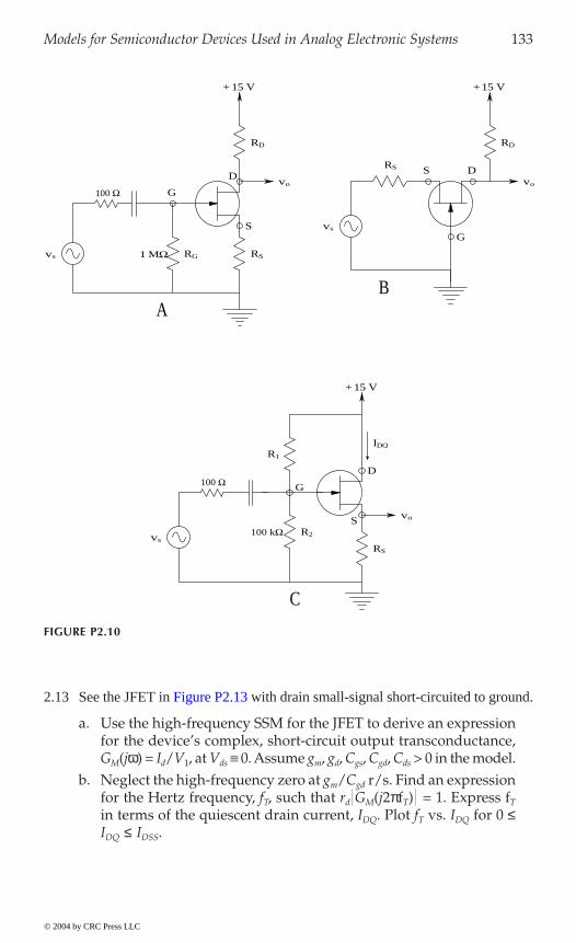
Models for Semiconductor Devices Used in Analog Electronic Systems 133
2.13
a. Use the high-frequency SSM for the JFET to derive an expressionfor the device’s complex, short-circuit output transconductance,GM(jw) = Id/V1, at Vds ∫ 0. Assume gm, gd, Cgs, Cgd, Cds > 0 in the model.
b. Neglect the high-frequency zero at gm/Cgd r/s. Find an expressionfor the Hertz frequency, fT, such that rd GM(j2pfT) = 1. Express fT
in terms of the quiescent drain current, IDQ. Plot fT vs. IDQ for 0 £IDQ £ IDSS.
FIGURE P2.10
RS
RG1 MΩ RS
+ 15 V
S
SD
D
D
S
G
+ 15 V
RS
100 Ω
vs
vs
vs
C
BA
IDQ
100 Ω G
G
100 kΩ R2
R1
vo
RD RD
+ 15 V
vo vo
© 2004 by CRC Press LLC
See the JFET in Figure P2.13 with drain small-signal short-circuited to ground.

134 Analysis and Application of Analog Electronic Circuits
FIGURE P2.11
FIGURE P2.12
FIGURE P2.13
RL
VCC
−VEE
2 IEQRE
ve
vo
Q1v1 Q2
RL
R1v1
vo
VDD
G1
G2
S1
S2
D1
D2
V1Id
G
R1 D
S
© 2004 by CRC Press LLC
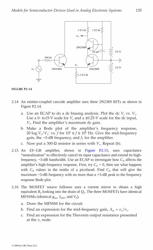
Models for Semiconductor Devices Used in Analog Electronic Systems 135
2.14 An emitter-coupled cascode amplifier uses three 2N2369 BJTs as shown inFigure P2.14.
a. Use an ECAP to do a dc biasing analysis. Plot the dc Vo vs. V1.Use a 0- to15-V scale for Vo and a ±0.25-V scale for the dc input,V1. Find the amplifier’s maximum dc gain.
b. Make a Bode plot of the amplifier’s frequency response,20 log Vo/V1 vs. f for 105 £ f £ 109 Hz. Give the mid-frequencygain, the -3-dB frequency, and fT for the amplifier.
c. Now put a 300-W resistor in series with V1. Repeat (b).
2.15“neutralization” to effectively cancel its input capacitance and extend its high-frequency, -3-dB bandwidth. Use an ECAP to investigate how CN affects theamplifier’s high-frequency response. First, try CN = 0, then see what happenswith CN values in the tenths of a picofarad. Find CN that will give themaximum -3-dB frequency with no more than a +3-dB peak to the frequencyresponse Bode plot.
2.16 The MOSFET source follower uses a current mirror to obtain a highequivalent RS looking into the drain of Q2. The three MOSFETs have identicalMFSSMs (identical gmo, IDSS, and VP).
a. Draw the MFSSM for the circuit.b. Find an expression for the mid-frequency gain, Avo = vo/v1.c. Find an expression for the Thevenin output resistance presented
at the vo node.
FIGURE P2.14
15 V
15 V
1.2 E3 Ω
1 E5 Ω1 E3 Ω
300 Ω
2N2369 2N2369
2N2369
10 µF
v1
vo
ve
© 2004 by CRC Press LLC
An EF–GB amplifier, shown in Figure P2.15, uses capacitance

136 Analysis and Application of Analog Electronic Circuits
2.17 A JFET circuit is used as a current sink for a differential amplifier’s “long tail.”
a. Use the high-frequency SSM for the FET to find an expressionfor the impedance looking into the FET’s drain, Zid(jw). (TheHiFSSM includes gm, gd, Cds, Cgd, Cgs.)
b. Find the FET’s short-circuit, dc drain current, IDsc. Assume theFET’s drain current is given by ID = IDSS (1 - VGS/VP)2. Assumesaturated drain operation. IDSS and VP are known.
FIGURE P2.15
FIGURE P2.16
RC RBRB
CN
100 Ω
VEE = −12 V
VCC = +12 V
ve1 µF
vo
Q1
V11 µF
Q2
Q1 = Q2 = 2N2369
RB = 1.8 MΩ
RE = 5.637 kΩ
RE
RC = 5.8 kΩ
vo
v1
VDD
Q2
Ibias Q1
Q3
S1
S2S3
D3 D2
D1
© 2004 by CRC Press LLC
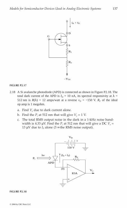
Models for Semiconductor Devices Used in Analog Electronic Systems 137
2.18 A Si avalanche photodiode (APD) is connected as shown in Figure P2.18. Thetotal dark current of the APD is ID = 10 nA, its spectral responsivity at l =512 nm is R(l) = 12 amps/watt at a reverse vD = -150 V. RF of the idealop amp is 1 megohm.
a. Find Vo due to dark current alone.b. Find the Pi at 512 nm that will give Vo = 1 V.c. The total RMS output noise in the dark in a 1-kHz noise band-
width is 4.33 mV. Find the Pi at 512 nm that will give a DC Vo =13 mV due to IP alone (3 ¥ the RMS noise output).
FIGURE P2.17
FIGURE P2.18
R2
R1
S
D
id + ID
G
−VSS
RF
APD
Pi
(ID + IP)
(0)
hν
Vo
IOA
150 V
VB
© 2004 by CRC Press LLC
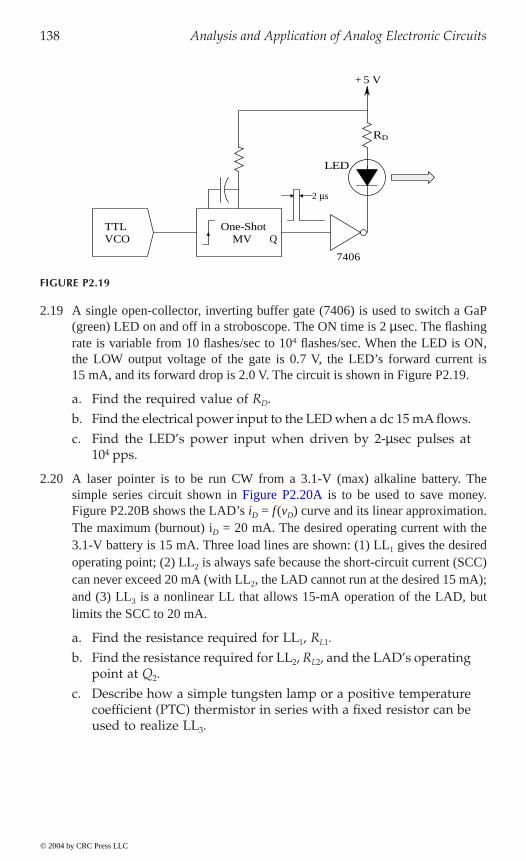
138 Analysis and Application of Analog Electronic Circuits
2.19 A single open-collector, inverting buffer gate (7406) is used to switch a GaP(green) LED on and off in a stroboscope. The ON time is 2 msec. The flashingrate is variable from 10 flashes/sec to 104 flashes/sec. When the LED is ON,the LOW output voltage of the gate is 0.7 V, the LED’s forward current is15 mA, and its forward drop is 2.0 V. The circuit is shown in Figure P2.19.
a. Find the required value of RD.b. Find the electrical power input to the LED when a dc 15 mA flows.c. Find the LED’s power input when driven by 2-msec pulses at
104 pps.
2.20 A laser pointer is to be run CW from a 3.1-V (max) alkaline battery. The
Figure P2.20B shows the LAD’s iD = f(vD) curve and its linear approximation.The maximum (burnout) iD = 20 mA. The desired operating current with the3.1-V battery is 15 mA. Three load lines are shown: (1) LL1 gives the desiredoperating point; (2) LL2 is always safe because the short-circuit current (SCC)can never exceed 20 mA (with LL2, the LAD cannot run at the desired 15 mA);and (3) LL3 is a nonlinear LL that allows 15-mA operation of the LAD, butlimits the SCC to 20 mA.
a. Find the resistance required for LL1, RL1.b. Find the resistance required for LL2, RL2, and the LAD’s operating
point at Q2.c. Describe how a simple tungsten lamp or a positive temperature
coefficient (PTC) thermistor in series with a fixed resistor can beused to realize LL3.
FIGURE P2.19
One-ShotMV
2 µs
LED
7406
TTLVCO
+ 5 V
RD
Q
© 2004 by CRC Press LLC
simple series circuit shown in Figure P2.20A is to be used to save money.
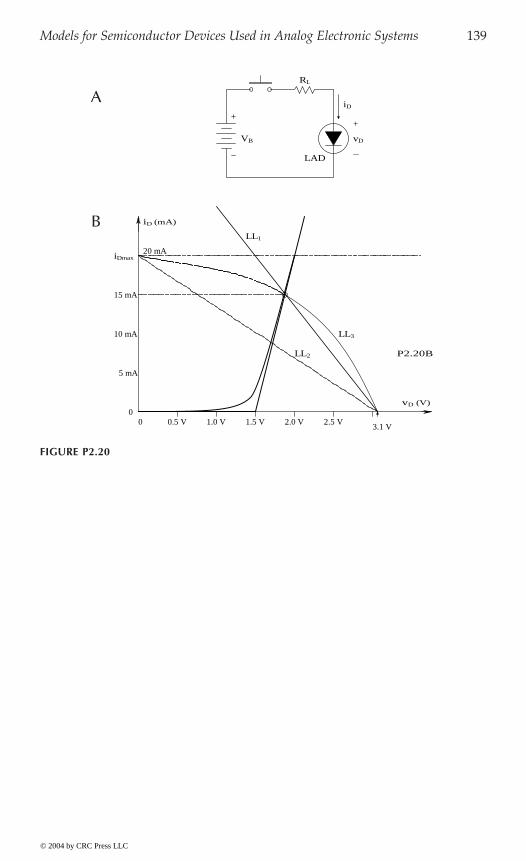
Models for Semiconductor Devices Used in Analog Electronic Systems 139
A
B
FIGURE P2.20
iD
vD
+
RL
VB
LAD
iDmax
iD (mA)
vD (V)
LL3
LL1
LL2
3.1 V1.5 V 2.0 V1.0 V0.5 V0
0
15 mA
10 mA
5 mA
20 mA
P2.20B
2.5 V
−
© 2004 by CRC Press LLC

141
3The Differential Amplifier
3.1 Introduction
The differential or difference amplifier (DA) is a cornerstone element in thedesign of most signal conditioning systems used in biomedical engineeringapplications, as well as in general instrumentation. All instrumentation andmedical isolation amplifiers are DAs as are nearly all operational amplifiers.Why are DAs so ubiquitous? The answer lies in their inherent ability to rejectunwanted dc levels, interference, and noise voltages common to both inputs.An ideal DA responds only to the so-called difference-mode signal at its twoinputs. Most DAs have a single-ended output voltage, Vo, given by thephasor relation:
Vo = A1V1 - A1¢¢¢¢ V1¢¢¢¢ (3.1)
Ideally, the gains A1 and A1¢¢¢¢ should be equal. In practice this does nothappen; thus:
Vo = AD V1d + AC V1c (3.2)
where:
Vid ∫ (V1 -V1¢ )/2 (difference-mode input voltage) (3.3A)
V1c ∫ (V1 + V1¢ )/2 (common-mode input voltage) (3.3B)
and AD is the complex difference mode gain and AC is the complex common-mode gain. It can easily be shown by vector summation that:
AD = A1 + A1¢¢¢¢ (3.4A)
AC = A1 - A1¢¢¢¢ (3.4B)
Clearly, if A1 = A1¢¢¢¢ , then AC Æ 0.
© 2004 by CRC Press LLC

142 Analysis and Application of Analog Electronic Circuits
3.2 DA Circuit Architecture
Figure 3.1 illustrates a simplified circuit of the Burr–Brown OPA606 JFET-INPUT op amp. Note that a pair of p-channel JFETS connected as a DA areused as a differential input headstage in the op amp. The single-ended signaloutput from the left-hand (inverting input) JFET drives the base (input) ofa BJT emitter–follower, which drives a second BJT connected as a grounded-base amplifier. Its output, in turn, drives the OA’s output stage.
To appreciate how the differential headstage works, consider the simple
Rs, Rd, and Rd¢ are shown as dc current sources and thus can be assumed tohave very high Norton resistances on the order of megohms. (See Northrop,1990, Section 5.2, for a description of active current sources and sinks used
model (MFSSM) of the JFET DA. To make the circuit bilaterally symmetric
analysis, two 2Rs resistors are put in parallel to replace the one Rs in theactual circuit. Note that all DC voltage sources are represented by small-signal grounds in all SSMS. The scalar AD and AC in Equation 3.2 are to beevaluated using the DCSSM. The simplest way to do this is to use thebisection theorem on the DA’s MFSSM. First, pure DM excitation is applied
FIGURE 3.1Simplified schematic of a Burr–Brown OPA606 JFET input DA.
© 2004 by CRC Press LLC
JFET DA circuit of Figure 3.2. Note that in the op amp schematic, the resistors
in IC DA designs.) Figure 3.3 illustrates the mid-frequency, small-signal
so that the bisection theorem (Northrop, 1990, Chapter 2) can be used in its
+ Vcc
−Vcc
Vo
−Vi
+Vi
Offset trim
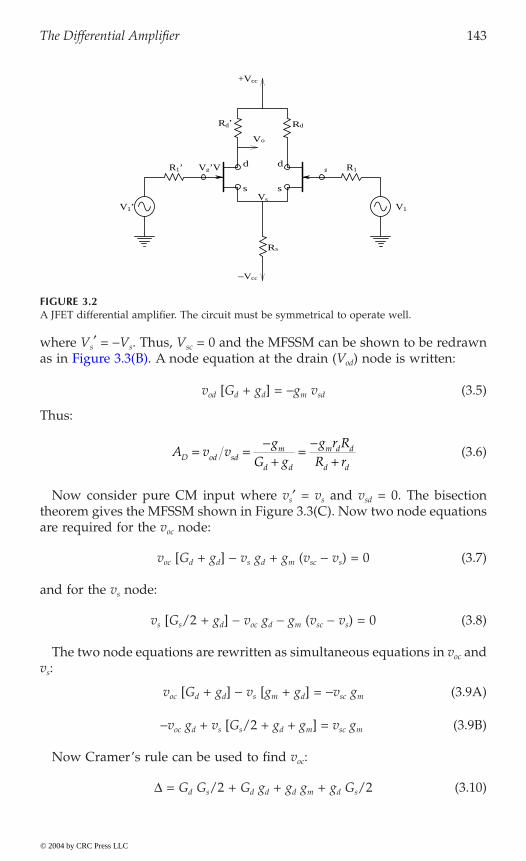
The Differential Amplifier 143
where Vs¢ = -Vs. Thus, Vsc = 0 and the MFSSM can be shown to be redrawnod) node is written:
vod [Gd + gd] = -gm vsd (3.5)
Thus:
(3.6)
Now consider pure CM input where vs¢ = vs and vsd = 0. The bisectiontheorem gives the MFSSM shown in Figure 3.3(C). Now two node equationsare required for the voc node:
voc [Gd + gd] - vs gd + gm (vsc - vs) = 0 (3.7)
and for the vs node:
vs [Gs/2 + gd] - voc gd - gm (vsc - vs) = 0 (3.8)
The two node equations are rewritten as simultaneous equations in voc andvs:
voc [Gd + gd] - vs [gm + gd] = -vsc gm (3.9A)
-voc gd + vs [Gs/2 + gd + gm] = vsc gm (3.9B)
Now Cramer’s rule can be used to find voc:
D = Gd Gs/2 + Gd gd + gd gm + gd Gs/2 (3.10)
FIGURE 3.2A JFET differential amplifier. The circuit must be symmetrical to operate well.
Vo
s
Rs
Vs
s
dd
V1V1’
R1
+Vcc
−Vcc
Rd’
R1’
Rd
Vg’V g
A v vg
G gg r R
R rD od sdm
d d
m d d
d d
= =-
+=
-+
© 2004 by CRC Press LLC
as in Figure 3.3(B). A node equation at the drain (V

144 Analysis and Application of Analog Electronic Circuits
D voc = - vsc gm Gs/2 (3.11)
After some algebra is used on Equation 3.10 and Equation 3.11, the dc andmid-frequency CM gain are obtained:
(3.12)
Note that AD AC. The significance of this inequality is examined next.
FIGURE 3.3s
is split into two, parallel 2Rs resistors. (B) Left-half-circuit of the DA following application ofthe bisection theorem for difference-mode excitation. Note that DM excitation makes vs = 0, sothe FET sources can be connected to small-signal ground. (C) Left-half-circuit of the DA fol-lowing application of the bisection theorem for common-mode excitation. See text for analysis.
gd gd
Rd
gd
Rd Rd
gd
A
B CRd
vo
vod vo
gmvgs
gmvgs vs
R1
gmvgs
vg R1
vgR1
gmvgs
vgR1
V1 V1 vs
vg’
(Axis of symmetry)
2Rs2Rs
S SV1’ V 1
D D
G G
2Rs
A v vg r R
r R R g RC oc scm d d
d d s m d
= =-
+ + +( )2 1
© 2004 by CRC Press LLC
(A) Mid-frequency small-signal model of the FET DA in Figure 3.2. R on the axis of symmetry
The Differential Amplifier 145
3.3 Common-Mode Rejection Ratio (CMRR)
The common-mode rejection ratio is an important figure of merit for differ-ential instrumentation and operational amplifiers. It is desired to be as largeas possible — ideally, infinite. The CMRR can be defined as:
(3.13)
Referring to Equation 3.2, it is clear that the CMRR can also be given by:
(3.14)
Note that the CMRR is a positive real number and is a function of frequency.Generally, the CMRR is given in decibels; i.e., CMRRdB = 20 log CMRR. Forthe MFSSM of the JFET DA in the preceding section, the CMRR is:
(3.15)
By making Rs very large by using a dynamic current source (Northrop, 1990),the CMRR of the simple JFET DA can be made about 104, or 80 dB.
The CMRRdB of a typical commercial differential instrumentation amplifier,e.g., a Burr–Brown INA111, is given as 90 dB at a gain of 1, 110 dB at a gainof 10, and 115 dB at gains from 102 to 103, all measured at 100 Hz. At a breakfrequency close to 200 Hz, the CMRRdB( f ) of the INA111 begins to roll offat approximately 20 dB/decade. For example, at a gain of 10, the CMRRdB
is down to 80 dB at 6 kHz. Decrease of CMRR with frequency is a generalproperty of all DAs. Because most input common-mode interference pickedup in biomedical applications of DAs is at dc or at power line frequency, itis important for such DAs to have a high CMRR that remains high (80 to120 dB) from dc to over 120 Hz. Modern IC instrumentation amplifiers easilymeet these criteria.
A major reason for the frequency dependence of the CMRR of DAs canbe attributed to the frequency dependence of AD( f ) and AC( f ), as described
CMRR required to give a certain DA output required to give the same DA output
∫vv
c
d
1
1
CMRR ∫( )( )
A
AD
C
f
f
CMRR =
-+
-+ + +( )
= ++( )+
g r RR rg r R
r R R g R
R g r
R r
m d d
d d
m d d
d d s m d
s m d
d d2 1
12 1
© 2004 by CRC Press LLC

146 Analysis and Application of Analog Electronic Circuits
in Section 3.5. Figure 3.4 illustrates typical Bode AR asymptote plots for theseparameters for a DA. For example, 20 log AD( f ) starts out at +40 dB at dc(gain of 100) and its Bode AR has its first break frequency at f3 Hz. Startingat -60 dB at dc (gain of 0.001), 20 log AC( f ) has a zero at approximately theopen-loop amplifier’s break frequency, f1; its Bode AR increases at +20dB/decade until it reaches a high frequency pole at f2, where it flattens out.Because the numerical CMRR = AD( f ) / AC( f ) , CMRRdB is simply:
CMRRdB = 20 log AD( f ) -20 log AC( f ) (3.16)
Thus, CMRRdB = 100 dB at dc and decreases at -20 dB/decade from f1 to f2,where it levels off at 30 dB. At f3 the CMRRdB again drops off at -20 dB/decade.Good DA design tries to make f1 as large as possible to extend the highCMRR region well into the frequency range of common-mode interferenceand noise.
FIGURE 3.4Typical Bode plot asymptotes for the common-mode gain frequency response, the difference-mode gain frequency response, and the common-mode rejection ratio frequency response.
f
AC(f)
dBCMRR
100
40
−60
10
3
AD(f)
0 f2 f3f1 f4
−6 dB/octave
−6 dB/octave
+6 dB/octave
© 2004 by CRC Press LLC
The Differential Amplifier 147
3.4 CM and DM Gain of Simple DA Stages at High Frequencies
3.4.1 Introduction
models for a JFET DA. Note that the small-signal, high-frequency model(SSHFM) for all FETs includes three small fixed capacitors: the drain-to-sourcecapacitance, Cds; the gate-to-drain capacitance, Cgd; and the gate-to-sourcecapacitance, Cgs. These capacitors, in particular Cgd, limit the high-frequencyperformance of the JFET DA. The small-signal, drain-source conductance,gd, is also quiescent operating point dependent; it is determined by theupward slope of the FET’s iD vs. vD curves as a function of vGS (see Northrop,1990, Section 1.6). The transconductance, gm, of the small-signal, voltage-
theorem. In the CM and DM HFSSMs, two lumped-parameter, small capac-itors can be seen. Cm is the collector-to-base capacitance, which is on the orderof a single pF, and is largely due to the depletion capacitance of the reverse-biased pn junction between collector and base; its value is a function of thecollector-to-base voltage. However, given a fixed quiescent operating point(Q-point) for the amplifier and small-signal, linear operation, it is possibleto approximate Cm with a fixed value for pencil-and-paper calculations. Cpmodels the somewhat larger capacitance of the forward-biased, base–emitterpn junction. It, too, depends on vBE and is generally approximated by itsvalue at VBEQ. Cm is generally on the order of 10 to 100 pF; it is larger inpower transistors that have larger BE junction areas.
Cs and Ce shunting the common source or emitter resistance to ground,respectively, is on the order of a single pF, but Rs and Re are generally theproduct of very dynamic current sources (with Norton resistances on theorder of tens of megohms), so these capacitances can be very important indetermining the high-frequency behavior of the CM gain.
3.4.2 High-Frequency Behavior of AC and AD for the JFET DA
It is necessary first to find an algebraic expression for the DM gain of theFET DA at high frequencies. This calculation requires the solution of twosimultaneous linear algebraic node equations (Figure 3.7(B)). The node volt-ages are vg and vod. All the currents are summed, leaving these nodes aspositive. After rearranging terms,
(3.17A)v s C C G v sC v Gg gd gs od gd d+( ) +[ ] - =1 1 1
© 2004 by CRC Press LLC
Figure 3.7(B) and Figure 3.7(C) illustrate the small-signal, high-frequency
Figure 3.5 illustrates a simple BJT DA. The hybrid-pi HFSSMs for CM andDM inputs are illustrated in Figure 3.6 after application of the bisection
controlled current source is also Q-point dependent, as shown in Chapter 2.
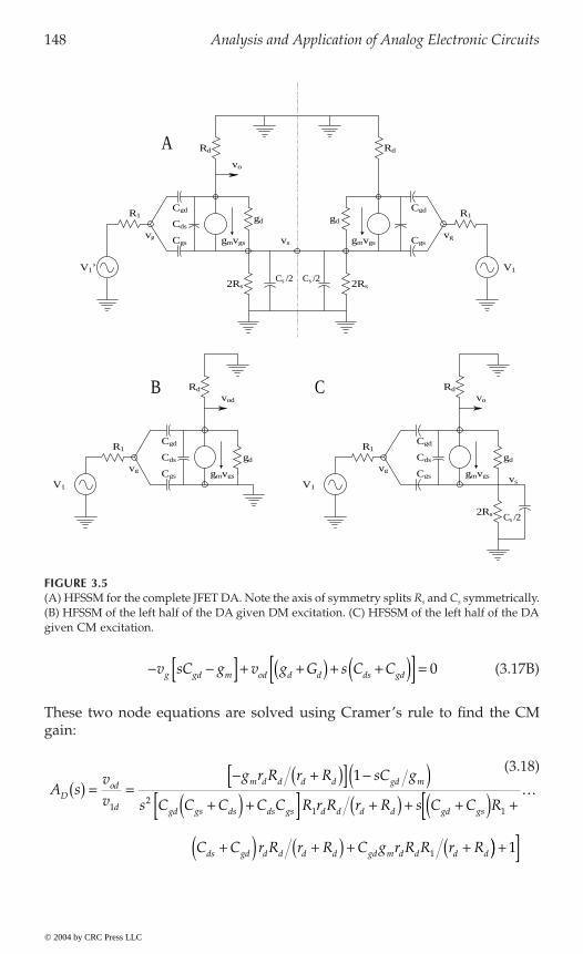
148 Analysis and Application of Analog Electronic Circuits
(3.17B)
These two node equations are solved using Cramer’s rule to find the CMgain:
FIGURE 3.5(A) HFSSM for the complete JFET DA. Note the axis of symmetry splits Rs and Cs symmetrically.(B) HFSSM of the left half of the DA given DM excitation. (C) HFSSM of the left half of the DAgiven CM excitation.
Cgd
Cdsgd gd
R1 R1
V1 V1
Rd
Cdsgd
V1
R1
Cgs
R1Cgd Cgd
gmvgs
Rd Rd
gd
2Rs2RsCs /2 Cs /2
Cgd
Cds
Cgs
A
B CRd
vo
vg vg
gmvgsvg vg
vod vo
Cgs gmvgs vs
gmvgs
V1’
Cgs vs
2Rs Cs /2
- -[ ] + +( ) + +( )[ ] =v sC g v g G s C Cg gd m od d d ds gd 0
A svv
g r R r R sC g
s C C C C C R r R r R s C C R
C C r R r R C g r R R r R
Dod
d
m d d d d gd m
gd gs ds ds gs d d d d gd gs
ds gd d d d d gd m d d d d
( ) = =- +( )[ ] -( )
+( ) +[ ] +( ) + +( ) +[+( ) +( ) + +(
12
1 1
1
1
)) + ]
º
1
(3.18)
© 2004 by CRC Press LLC

The Differential Amplifier 149
AD(s) is seen to have a quadratic denominator and a curious high-fre-quency, right-half s-plane zero at gm/Cgd r/s. Its low frequency gain is thesame as found in Section 3.2, i.e., -gm rd Rd/(rd + Rd). To find the poles, it isexpedient to insert typical numerical parameter values for a JFET DA(Northrop, 1990). Let Cgd = 3 pF; Cgs = 3 pF; Cds = 0.2 pF; Cs = 3 pF; gm = 0.005S; rd = 105 ohms; Rd = 5 ¥ 103 ohms; Re = 106 ohms (active current source);and R1 = 103 ohms. After numerical calculations, the zero is found to be at265 MHz and the two real poles are at 1.687 and 309 MHz. The dc DM gainis -23.8, or 27.5 dB. Thus 20 log AD( f ) is down by -3 dB at 1.687 MHz.
C
tunately, according to the bisection theorem, the voltage, vs, on the axis ofsymmetry is non-zero, so a third (vs) node must have a node equation writtenwhen finding voc. The three node equations are:
(3.18A)
(3.18B)
(3.18C)
FIGURE 3.6A BJT DA. Note symmetry. The resistors Re¢ are used to raise the DM input resistance.
R1 R1
Rb RbRc Rc
Re
V1’ V 1
Vb’ V b
Ve
Vo
+Vcc
−Vcc
Re’ Re’
v G s C C v s C v s C v Gg gd gs oc gd s gs c1 1 1+ +( )[ ] - [ ] - [ ] =
- -[ ] + +( ) + +( )[ ] - + +[ ] =v s C g v g G s C C v g g s Cg gd m oc d d ds gd s m d ds 0
- +[ ] - +[ ] +
+ +( ) + + +[ ] =
v g sC v g sC
v s C C C G g g
g m gs oc d ds
s s ds gs s d m 2 2 0
© 2004 by CRC Press LLC
To find A (s) for the JFET DA, the HFSSM of Figure 3.7(C) is used. Unfor-
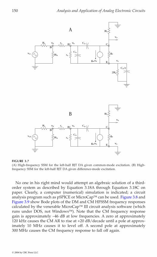
150 Analysis and Application of Analog Electronic Circuits
No one in his right mind would attempt an algebraic solution of a third-order system as described by Equation 3.18A through Equation 3.18C onpaper. Clearly, a computer (numerical) simulation is indicated; a circuit
calculated by the venerable MicroCap III circuit analysis software (whichruns under DOS, not Windows). Note that the CM frequency responsegain is approximately –46 dB at low frequencies. A zero at approximately120 kHz causes the CM AR to rise at +20 dB/decade until a pole at approx-imately 10 MHz causes it to level off. A second pole at approximately300 MHz causes the CM frequency response to fall off again.
FIGURE 3.7(A) High-frequency SSM for the left-half BJT DA given common-mode excitation. (B) High-frequency SSM for the left-half BJT DA given difference-mode excitation.
gmvb
go
go
gmvb
rx
rx
rπ
rπ
Rs
Rs
Cπ
Cπ
Cµ
Cµ
Rc
Rc
vo
2Re
Ce/2
vb vb
vbvb
ve
ve
vo
vsd
vsc Rb
Rb
B
BB’
B’ C
C
E
E
A
B
© 2004 by CRC Press LLC
analysis program such as pSPICE or MicroCap can be used. Figure 3.8 andFigure 3.9 show Bode plots of the DM and CM HFSSM frequency responses
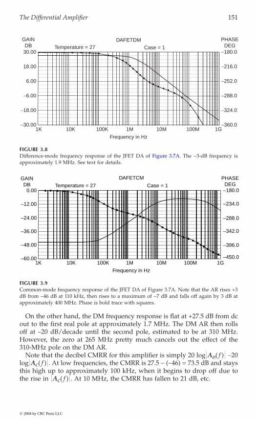
The Differential Amplifier 151
On the other hand, the DM frequency response is flat at +27.5 dB from dcout to the first real pole at approximately 1.7 MHz. The DM AR then rollsoff at –20 dB/decade until the second pole, estimated to be at 310 MHz.However, the zero at 265 MHz pretty much cancels out the effect of the310-MHz pole on the DM AR.
Note that the decibel CMRR for this amplifier is simply 20 log AD( f ) -20log AC( f ) . At low frequencies, the CMRR is 27.5 - (-46) = 73.5 dB and staysthis high up to approximately 100 kHz, when it begins to drop off due tothe rise in AC( f ) . At 10 MHz, the CMRR has fallen to 21 dB, etc.
FIGURE 3.8
approximately 1.9 MHz. See text for details.
FIGURE 3.9Common-mode frequency response of the JFET DA of Figure 3.7A. Note that the AR rises +3dB from -46 dB at 110 kHz, then rises to a maximum of -7 dB and falls off again by 3 dB atapproximately 400 MHz. Phase is bold trace with squares.
© 2004 by CRC Press LLC
Difference-mode frequency response of the JFET DA of Figure 3.7A. The -3-dB frequency is
Frequency in Hz
Case = 1
DAFETDMTemperature = 27
GAINDB
30.00
18.00
6.00
−6.00
−18.00
−30.001K 10K 1M 10M 100M 1G100K
−360.0
−324.0
−288.0
−252.0
−216.0
−180.0
PHASEDEG
GAINDB
0.00
–24.00
–12.00
–36.00
–48.00
–60.00
Temperature = 27
DAFETCM
Case = 1PHASE
DEG–180.0
–234.0
–288.0
–342.0
–396.0
–450.0
Frequency in Hz
10K 100K 10M 100M 1G1M1K
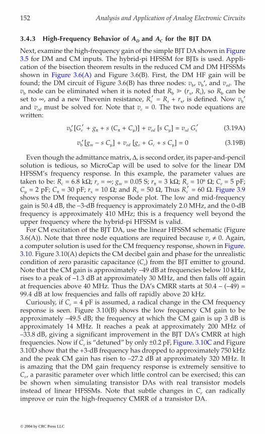
152 Analysis and Application of Analog Electronic Circuits
3.4.3 High-Frequency Behavior of AD and AC for the BJT DA
cation of the bisection theorem results in the reduced CM and DM HFSSMs
found; the DM circuit of Figure 3.6(B) has three nodes: vb, vb¢, and vod. Thevb node can be eliminated when it is noted that Rb (rx, Rs), so Rb can beset to , and a new Thevenin resistance, Rs¢ = Rs + rx, is defined. Now vb¢and vod must be solved for. Note that ve = 0. The two node equations arewritten:
vb¢ [Gs¢ + gp + s (Cp + Cm)] + vod [s Cm] = vsd Gs¢ (3.19A)
vb¢ [gm - s Cm] + vod [go + Gc + s Cm] = 0 (3.19B)
Even though the admittance matrix, D, is second order, its paper-and-pencilsolution is tedious, so MicroCap will be used to solve for the linear DMHFSSM’s frequency response. In this example, the parameter values aretaken to be: Rc = 6.8 kW; ro = ; gm = 0.05 S; rp = 3 kW; Re = 106 W; Ce = 5 pF;
m p x s s¢shows the DM frequency response Bode plot. The low and mid-frequencygain is 50.4 dB, the -3-dB frequency is approximately 2.0 MHz, and the 0-dBfrequency is approximately 410 MHz; this is a frequency well beyond theupper frequency where the hybrid-pi HFSSM is valid.
For CM excitation of the BJT DA, use the linear HFSSM schematic (Figure3.6(A)). Note that three node equations are required because ve π 0. Again,
condition of zero parasitic capacitance (Ce) from the BJT emitter to ground.Note that the CM gain is approximately –49 dB at frequencies below 10 kHz,rises to a peak of –1.3 dB at approximately 30 MHz, and then falls off againat frequencies above 40 MHz. Thus the DA’s CMRR starts at 50.4 – (-49) =99.4 dB at low frequencies and falls off rapidly above 20 kHz.
Curiously, if Ce = 4 pF is assumed, a radical change in the CM frequencyresponse is seen. Figure 3.10(B) shows the low frequency CM gain to beapproximately –49.5 dB; the frequency at which the CM gain is up 3 dB isapproximately 14 MHz. It reaches a peak at approximately 200 MHz of–33.8 dB, giving a significant improvement in the BJT DA’s CMRR at high
e
3.10D show that the +3-dB frequency has dropped to approximately 750 kHzand the peak CM gain has risen to –27.2 dB at approximately 320 MHz. Itis amazing that the DM gain frequency response is extremely sensitive toCe, a parasitic parameter over which little control can be exercised; this canbe shown when simulating transistor DAs with real transistor modelsinstead of linear HFSSMs. Note that subtle changes in Ce can radicallyimprove or ruin the high-frequency CMRR of a transistor DA.
© 2004 by CRC Press LLC
Next, examine the high-frequency gain of the simple BJT DA shown in Figure3.5 for DM and CM inputs. The hybrid-pi HFSSM for BJTs is used. Appli-
C = 2 pF; C = 30 pF; r = 10 W; and R = 50 W, Thus R = 60 W. Figure 3.9
a computer solution is used for the CM frequency response, shown in Figure.3.10. Figure 3.10(A) depicts the CM decibel gain and phase for the unrealistic
frequencies. Now if C is “detuned” by only ±0.2 pF, Figure. 3.10C and Figure
shown in Figure 3.6(A) and Figure 3.6(B). First, the DM HF gain will be
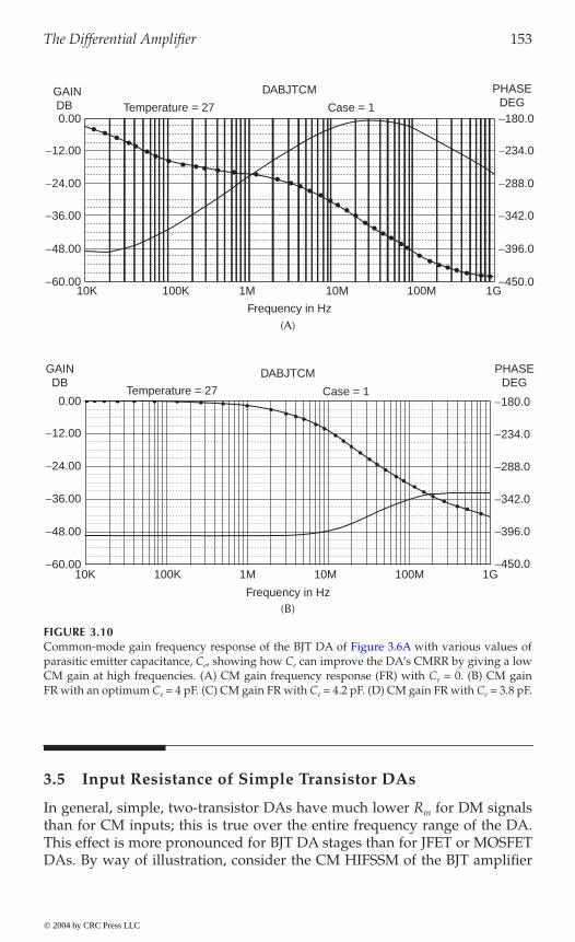
The Differential Amplifier 153
3.5 Input Resistance of Simple Transistor DAs
In general, simple, two-transistor DAs have much lower Rin for DM signalsthan for CM inputs; this is true over the entire frequency range of the DA.This effect is more pronounced for BJT DA stages than for JFET or MOSFETDAs. By way of illustration, consider the CM HIFSSM of the BJT amplifier
FIGURE 3.10
parasitic emitter capacitance, Ce, showing how Ce can improve the DA’s CMRR by giving a lowCM gain at high frequencies. (A) CM gain frequency response (FR) with Ce = 0. (B) CM gainFR with an optimum Ce = 4 pF. (C) CM gain FR with Ce = 4.2 pF. (D) CM gain FR with Ce = 3.8 pF.
© 2004 by CRC Press LLC
Common-mode gain frequency response of the BJT DA of Figure 3.6A with various values of
(A)
(B)
GAIN DB Temperature = 27
DABJTCM
Frequency in Hz
Case = 1
PHASEDEG
0.00
−12.00
−24.00
−36.00
−48.00
−60.0010K 100K 1M 10M 100M 1G
−180.0
−234.0
−288.0
−342.0
−396.0
−450.0
0.00
−12.00
−24.00
−36.00
−48.00
−60.0010K 100K 1M
Frequency in Hz
10M 100M 1G−450.0
−396.0
−342.0
−288.0
−234.0
−180.0
PHASEDEG
Case = 1
DABJTCM
Temperature = 27
GAINDB
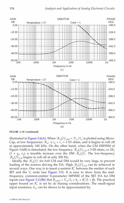
154 Analysis and Application of Analog Electronic Circuits
in( f ) DM = Vsc/Isc is plotted using Micro-Cap, at low frequencies Rin @ rp + rx = 3 E3 ohms, and it begins to roll offat approximately 100 kHz. On the other hand, when the CM HIFSSM ofFigure 3.6(B) is stimulated, the low frequency Rin( f ) CM @ 3 E8 ohms, or 2RE
(1 + gm rp), a sizeable increase over the DM Rin( f ) . The low-frequencyRin( f ) CM begins to roll off at only 200 Hz.
Ideally, the Rin( f ) for both CM and DM would be very large, to preventloading of the sources driving the DA. High Rin( f ) DM can be achieved inseveral ways. One way is to insert a resistor Re¢ between the emitter of each
e
frequency, common-emitter h-parameter MFSSM of the BJT DA for DMinDM = Vsd/Ib = hie + Re¢ (1 + b). The practical
upper bound on Re¢ is set by dc biasing considerations. The small-signalinput resistance, hie, can be shown to be approximated by:
FIGURE 3.10 (continued)
© 2004 by CRC Press LLC
BJT and the V node (see Figure 3.5). It is easy to show from the mid-
inputs (see Figure 3.11(B)) that R
illustrated in Figure 3.6(A). When R
(C)
(D)
10K 100K
Frequency in Hz
10M 100M 1G−450.0
−396.0
−342.0
−288.0
−234.0
−180.0
PHASEDEGCase = 1
DABJTCM
Temperature = 27
GAINDB
0.00
−12.00
−24.00
−36.00
−48.00
−60.001M
10K 100K
Frequency in Hz
10M 100M 1G−450.0
−396.0
−342.0
−288.0
−234.0
−180.0
PHASEDEGCase = 1
DABJTCM
Temperature = 27GAINDB
0.00
−12.00
−24.00
−36.00
−48.00
−60.001M
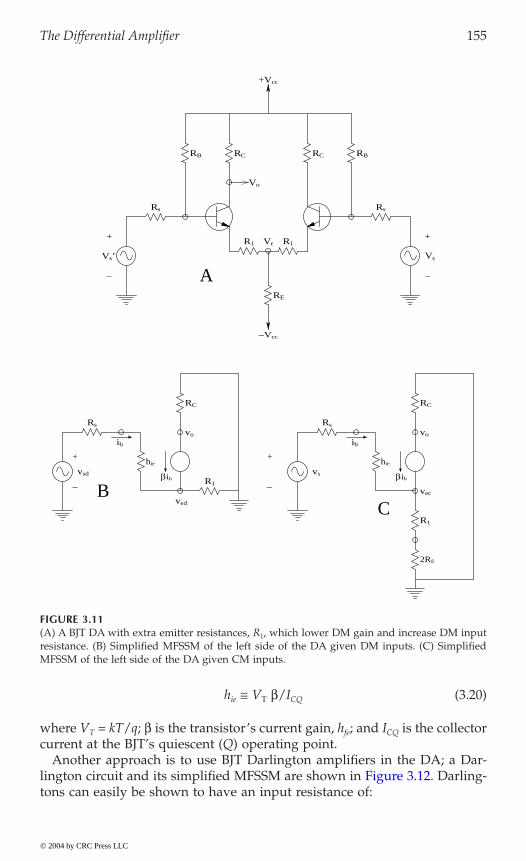
The Differential Amplifier 155
hie @ VT b/ICQ (3.20)
where VT = kT/q; b is the transistor’s current gain, hfe; and ICQ is the collectorcurrent at the BJT’s quiescent (Q) operating point.
Another approach is to use BJT Darlington amplifiers in the DA; a Dar-
tons can easily be shown to have an input resistance of:
FIGURE 3.11(A) A BJT DA with extra emitter resistances, R1, which lower DM gain and increase DM inputresistance. (B) Simplified MFSSM of the left side of the DA given DM inputs. (C) SimplifiedMFSSM of the left side of the DA given CM inputs.
+Vcc
Ve
RE
Vo
RB RBRC RC
Rs Rs
V Vs’ s
R1 R1+ +
-
-Vcc
Rs Rs
hie hie
RC RC
bib bibR1
R1
vsd
+ +
vs
- -
vovo
vec
ved
ibib
A-
B
2RE
C
© 2004 by CRC Press LLC
lington circuit and its simplified MFSSM are shown in Figure 3.12. Darling-

156 Analysis and Application of Analog Electronic Circuits
Rin = hie1 + hie2(1 + b1) (3.21)
If an emitter resistor, R1, is used as in the first case, Rin can be shown to be:
Rin = hie1 + (1 + hfe1)[hie2 + R1(1 + hfe2)] @ hfe1 hfe2 R1 (3.22)
Thus, if hfe1 = hfe2 = 100 and R1 = 200 W, Rin > 2 MW.
FIGURE 3.12
of the Darlington valid for DM excitation of the DA. The input resistance for the DarlingtonDA given DM excitation is derived in the text.
ib
hfe ib
hfe ib
R1
ve2
ib = ib1(1 + hfe1)
B2
E1
ib (1 + hfe )
C2
C1B1
Rc
Q1
Q2
R1
ve2
Rc
VCC
ib
vs
vs
A
B
( oe = hre = 0
hie1
hie2
© 2004 by CRC Press LLC
(A) A Darlington stage that can replace the left-hand BJT in the DA of Figure 3.11A. (B) MFSSM
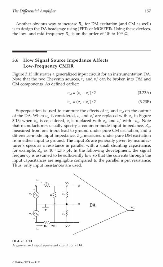
The Differential Amplifier 157
Another obvious way to increase Rin for DM excitation (and CM as well)is to design the DA headstage using JFETs or MOSFETs. Using these devices,the low- and mid-frequency Rin is on the order of 109 to 1012 W.
3.6 How Signal Source Impedance Affects Low-Frequency CMRR
Figure 3.13 illustrates a generalized input circuit for an instrumentation DA.Note that the two Thevenin sources, vs and vs¢ can be broken into DM andCM components. As defined earlier:
vsd ∫ (vs - vs¢ )/2 (3.23A)
vsc ∫ (vs + vs¢ )/2 (3.23B)
Superposition is used to compute the effects of vsc and vsd on the outputof the DA. When vsc is considered, vs and vs¢ are replaced with vsc in Figure3.13; when vsd is considered, vs is replaced with vsd and vs¢ with -vsd. Notethat manufacturers usually specify a common-mode input impedance, Zic,measured from one input lead to ground under pure CM excitation, and adifference-mode input impedance, Zid, measured under pure DM excitationfrom either input to ground. The input Zs are generally given by manufac-turer’s specs as a resistance in parallel with a small shunting capacitance,for example, Zic as 1011 W5 pF. In the following development, the signalfrequency is assumed to be sufficiently low so that the currents through theinput capacitances are negligible compared to the parallel input resistance.Thus, only input resistances are used.
FIGURE 3.13A generalized input equivalent circuit for a DA.
DA
R1Rc
Rc
Rs
+
Vo
Vs
Vs’
+
V1
V1’Rs + ∆RIs’
Is
© 2004 by CRC Press LLC
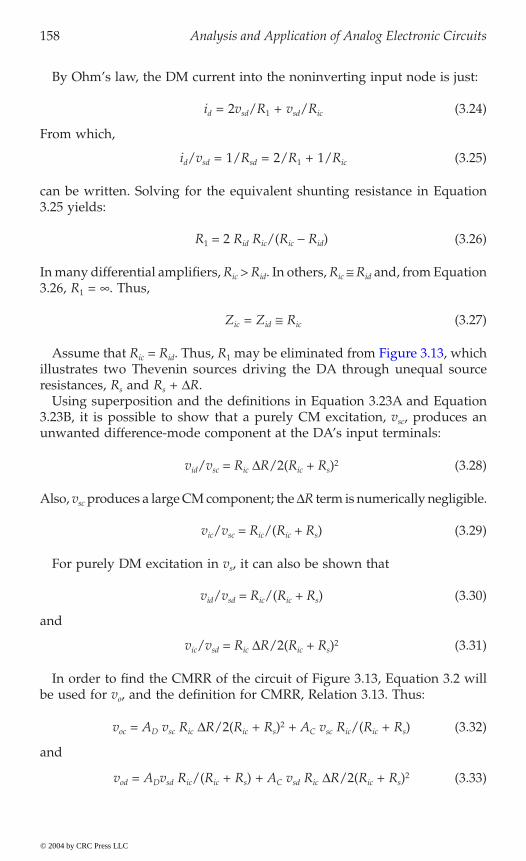
158 Analysis and Application of Analog Electronic Circuits
By Ohm’s law, the DM current into the noninverting input node is just:
id = 2vsd/R1 + vsd/Ric (3.24)
From which,
id/vsd = 1/Rsd = 2/R1 + 1/Ric (3.25)
can be written. Solving for the equivalent shunting resistance in Equation3.25 yields:
R1 = 2 Rid Ric/(Ric - Rid) (3.26)
In many differential amplifiers, Ric > Rid. In others, Ric @ Rid and, from Equation3.26, R1 = . Thus,
Zic = Zid @ Ric (3.27)
ic id 1
illustrates two Thevenin sources driving the DA through unequal sourceresistances, Rs and Rs + DR.
Using superposition and the definitions in Equation 3.23A and Equation3.23B, it is possible to show that a purely CM excitation, vsc, produces anunwanted difference-mode component at the DA’s input terminals:
vid/vsc = Ric DR/2(Ric + Rs)2 (3.28)
Also, vsc produces a large CM component; the DR term is numerically negligible.
vic/vsc = Ric/(Ric + Rs) (3.29)
For purely DM excitation in vs, it can also be shown that
vid/vsd = Ric/(Ric + Rs) (3.30)
and
vic/vsd = Ric DR/2(Ric + Rs)2 (3.31)
In order to find the CMRR of the circuit of Figure 3.13, Equation 3.2 willbe used for vo, and the definition for CMRR, Relation 3.13. Thus:
voc = AD vsc Ric DR/2(Ric + Rs)2 + AC vsc Ric/(Ric + Rs) (3.32)
and
vod = ADvsd Ric/(Ric + Rs) + AC vsd Ric DR/2(Ric + Rs)2 (3.33)
© 2004 by CRC Press LLC
Assume that R = R . Thus, R may be eliminated from Figure 3.13, which
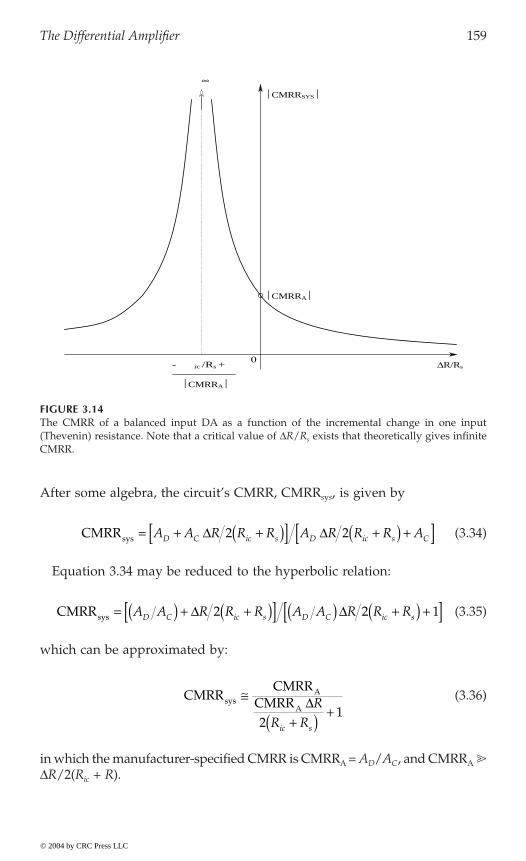
The Differential Amplifier 159
After some algebra, the circuit’s CMRR, CMRRsys, is given by
(3.34)
Equation 3.34 may be reduced to the hyperbolic relation:
(3.35)
which can be approximated by:
(3.36)
in which the manufacturer-specified CMRR is CMRRA = AD/AC, and CMRRA DR/2(Ric + R).
FIGURE 3.14The CMRR of a balanced input DA as a function of the incremental change in one input(Thevenin) resistance. Note that a critical value of DR/Rs exists that theoretically gives infiniteCMRR.
0
CMRRA
CMRRSYS
∞
CMRRA
∆R/Rs- ic /Rs +
CMRRsys = + +( )[ ] +( ) +[ ]A A R R R A R R R AD C ic s D ic s CD D2 2
CMRRsys = ( ) + +( )[ ] ( ) +( ) +[ ]A A R R R A A R R RD C ic s D C ic sD D2 2 1
CMRRCMRR
CMRRsysA
A@
+( ) +DR
R Ric s21
© 2004 by CRC Press LLC
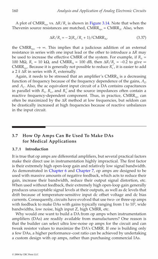
160 Analysis and Application of Analog Electronic Circuits
A plot of CMRRsys s
Thevenin source resistances are matched, CMRRsys = CMRRA. Also, when
DR/Rs = - 2(Ric/Rs + 1)/CMRRA, (3.37)
the CMRRsys Æ . This implies that a judicious addition of an externalresistance in series with one input lead or the other to introduce a DR maybe used to increase the effective CMRR of the system. For example, if Ric =100 MW, Rs = 10 kW, and CMRRA = 100 dB, then DR/Rs = -0.2 to give CMRRsys. Because it is generally not possible to reduce Rs¢ , it is easier to adda 2 k DR in series with Rs externally.
Again, it needs to be stressed that an amplifier’s CMRRA is a decreasingfunction of frequency because of the frequency dependence of the gains, AD
and AC. Also, the ac equivalent input circuit of a DA contains capacitancesin parallel with R1, Ric, and Ric¢ and the source impedances often contain areactive frequency-dependent component. Thus, in practice, CMRRsys canoften be maximized by the DR method at low frequencies, but seldom canbe drastically increased at high frequencies because of reactive unbalancesin the input circuit.
3.7 How Op Amps Can Be Used To Make DAs for Medical Applications
3.7.1 Introduction
It is true that op amps are differential amplifiers, but several practical factorsmake their direct use in instrumentation highly impractical. The first factoris their extremely high open-loop gain and relatively low signal bandwidth.
used with massive amounts of negative feedback, which acts to reduce theirgain, increase their bandwidth, reduce their output signal distortion, etc.When used without feedback, their extremely high open-loop gain generallyproduces unacceptable signal levels at their outputs, as well as dc levels thatdrift because of temperature-sensitive input dc offset voltage and dc biascurrents. Consequently, circuits have evolved that use two- or three-op ampswith feedback to make DAs with gains typically ranging from 1 to 103, widebandwidths, low noise, high input Z, high CMRR, etc.
Why would one want to build a DA from op amps when instrumentationamplifiers (DAs) are readily available from manufacturers? One reason isthat the builder can select ultra low-noise op amps for the circuit and cantweak resistor values to maximize the DA’s CMRR. If one is building onlya few DAs, a higher performance–cost ratio can be achieved by undertakinga custom design with op amps, rather than purchasing commercial IAs.
© 2004 by CRC Press LLC
vs. DR/R is shown in Figure 3.14. Note that when the
As demonstrated in Chapter 6 and Chapter 7, op amps are designed to be
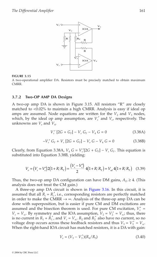
The Differential Amplifier 161
3.7.2 Two-OP AMP DA Designs
A two-op amp DA is shown in Figure 3.15. All resistors “R” are closelymatched to <0.02% to maintain a high CMRR. Analysis is easy if ideal opamps are assumed. Node equations are written for the V2 and V3 nodes,which, by the ideal op amp assumption, are Vs¢ and Vs, respectively. Theunknowns are Vo and V4.
Vs¢ [2G + GF] - Vs GF - V4 G = 0 (3.38A)
-Vs¢ GF + Vs [2G + GF] - Vo G - V4 G = 0 (3.38B)
Clearly, from Equation 3.38A, V4 G = Vs¢[2G + GF] - Vs GF. This equation issubstituted into Equation 3.38B, yielding:
(3.39)
Thus, the two-op amp DA configuration can have DM gains, AD ≥ 4. (Thisanalysis does not treat the CM gain.)
assumed that all Rj = Rj¢, i.e., corresponding resistors are perfectly matchedin order to make the CMRR Æ . Analysis of the three-op amp DA can bedone with superposition, but is easier if pure CM and DM excitations areassumed and the bisection theorem is used. For pure CM excitation, Vs¢ =Vs = Vsc. By symmetry and the IOA assumption, V2 = V2¢ = Vsc; thus, thereis no current in R1 + R1¢ , and Vc = Vsc. R2 and R2¢ also have no current, so novoltage drop occurs across these feedback resistors and thus V3 = V3¢ = Vsc.When the right-hand IOA circuit has matched resistors, it is a DA with gain:
Vo = (V3 - V3¢ )(R4/R3) (3.40)
FIGURE 3.15A two-operational amplifier DA. Resistors must be precisely matched to obtain maximumCMRR.
IOA
IOA
Vo
V2
V4
RFRR
V3
R
Vs’
Vs
V V V R RV V
R R V R Ro s s Fs s
F sd F= = ¢( ) +( ) =- ¢( ) +( ) = +( )2 12
4 1 4 1
© 2004 by CRC Press LLC
A three-op amp DA circuit is shown in Figure 3.16. In this circuit, it is
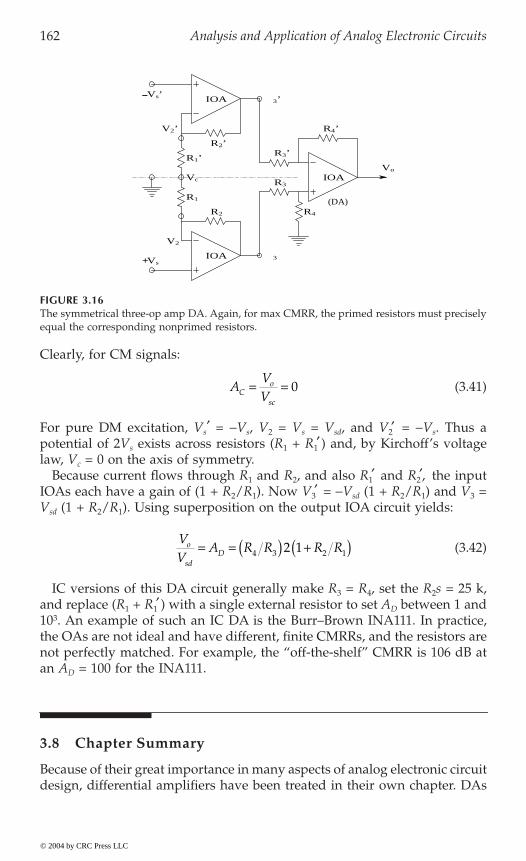
162 Analysis and Application of Analog Electronic Circuits
Clearly, for CM signals:
(3.41)
For pure DM excitation, Vs¢ = -Vs, V2 = Vs = Vsd, and V2¢ = -Vs. Thus apotential of 2Vs exists across resistors (R1 + R1¢ ) and, by Kirchoff’s voltagelaw, Vc = 0 on the axis of symmetry.
Because current flows through R1 and R2, and also R1¢ and R2¢, the inputIOAs each have a gain of (1 + R2/R1). Now V3¢ = -Vsd (1 + R2/R1) and V3 =Vsd (1 + R2/R1). Using superposition on the output IOA circuit yields:
(3.42)
IC versions of this DA circuit generally make R3 = R4, set the R2s = 25 k,and replace (R1 + R1¢ ) with a single external resistor to set AD between 1 and103. An example of such an IC DA is the Burr–Brown INA111. In practice,the OAs are not ideal and have different, finite CMRRs, and the resistors arenot perfectly matched. For example, the “off-the-shelf” CMRR is 106 dB atan AD = 100 for the INA111.
3.8 Chapter Summary
Because of their great importance in many aspects of analog electronic circuitdesign, differential amplifiers have been treated in their own chapter. DAs
FIGURE 3.16The symmetrical three-op amp DA. Again, for max CMRR, the primed resistors must preciselyequal the corresponding nonprimed resistors.
AVVC
o
sc
= = 0
VV
A R R R Ro
sdD= = ( ) +( )4 3 2 12 1
© 2004 by CRC Press LLC
V2’
R1’
R3
R3’
R4’
R4
IOAVo
Vc
R1
Vs’ IOA 3’
Vs
V2
IOA 3
R2
R2’
+
−−−−
(DA)

The Differential Amplifier 163
are essential electronic subsystems for ICs such as op amps, instrumentationamplifiers, and analog voltage comparators. DAs are widely used in instru-mentation systems to condition signals because of their ability to reject, bysubtraction, interference and noise that are exactly common to both inputs.
In describing DA circuit architecture, important definitions of differentialand common-mode input signals, differential and common-mode gains, andcommon-mode rejection ratio (CMRR) as a DA figure of merit were introduced.Internal and external factors affecting the DA’s CMRR at low frequencieswere described.
The mid- and high-frequency behavior of DA difference-mode and common-mode gains were explored by circuit simulation and factors affecting theCMRR at high frequencies were discussed. Circuits using two- and three-opamps to make instrumentation DAs were described and analyzed.
Home Problems
3.1 A pair of matched JFETs and an ideal op amp are used to make a DA as shownin Figure P3.1. Both JFETs are described at mid-frequencies by the simpleNorton (gm, gd) MFSSM.
a. Draw the complete MFSSM for the DA. Note that the MFSSMtreats all dc voltage sources as small signal grounds and all dccurrent sources as open circuits.
b. Use superposition to derive an expression for vo = f(v1, v2). Showwhat happens to vo when RS is replaced with an ideal dc currentsource.
FIGURE P3.1
vo
v1 v2
vs
−VSS
VDD
RS
RF
IOA
S S
D
id2
© 2004 by CRC Press LLC

164 Analysis and Application of Analog Electronic Circuits
3.2 The schematic of a JFET/BJT cascode DA is shown in Figure P3.2. In thisDA, Q1 = Q2 with hoe = hre = 0, hfe = 120, ICQ = 1 mA, RC = 7 kW, Rs = 25 MW(dynamic load), and RB = 1.24 MW. Also, Q3 = Q4 with gm = 5 ¥ 10-3 S, gd =1 ¥ 10-4 S.
a. Use the bisection theorem to draw the MFSSMs for pure CM andpure DM excitation.
b. Find an expression for the CM gain, vo/v1c.c. Find an expression for the DA’s DM gain, vo/v1d.d. Find an expression for and evaluate numerically the DA’s CMRR.
3.3VINV is an ideal VCVS with a gain of -1. The common emitters use an activecurrent sink that can be replaced by its Norton equivalent of a 2.0125-mAcurrent source in parallel with a 2-MW resistor and a small shunt capacitanceto ground, CE.
a. Use an ECAP to make a Bode plot of the DM gain, Vo/V1d, vs. ffrom 10 kHz to 10 GHz. Give values for the mid-frequency gain,the upper -3-dB frequency, and fT.
b. Figure P3.3B illustrates the DA given pure CM excitation. Nowthe capacitor, CE, will affect the CM high frequency response.Make a Bode plot of the CM gain, Vo/V1c over 1 kHz to 1 GHzwith CE ∫ 0.
FIGURE P3.2
vs
v1’
vo vo’
RC RCRB RB
RS
-VSS
VCC
S S
D D
ve’ve
Q1 Q2
v1Q3 Q4
© 2004 by CRC Press LLC
Figure P3.3A shows the schematic of a 2N2369 DA given DM excitation.
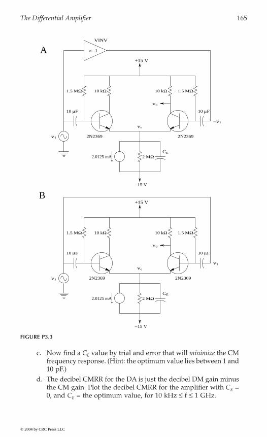
The Differential Amplifier 165
c. Now find a CE value by trial and error that will minimize the CMfrequency response. (Hint: the optimum value lies between 1 and10 pF.)
d. The decibel CMRR for the DA is just the decibel DM gain minusthe CM gain. Plot the decibel CMRR for the amplifier with CE =0, and CE = the optimum value, for 10 kHz £ f £ 1 GHz.
FIGURE P3.3
1.5 MW 1.5 MW10 kW 10 kW
10 mF10 mF
2.0125 mA 2 MW
ve
vo
¥ -1
v1
-v1
1.5 MW 1.5 MW10 kW 10 kW
10 mF10 mF
2.0125 mA 2 MW
ve
vo
v1
+15 V
+15 V
-15 V
2N2369 2N2369
v1 2N2369 2N2369
-15 V
CE
CE
VINV
A
B
© 2004 by CRC Press LLC
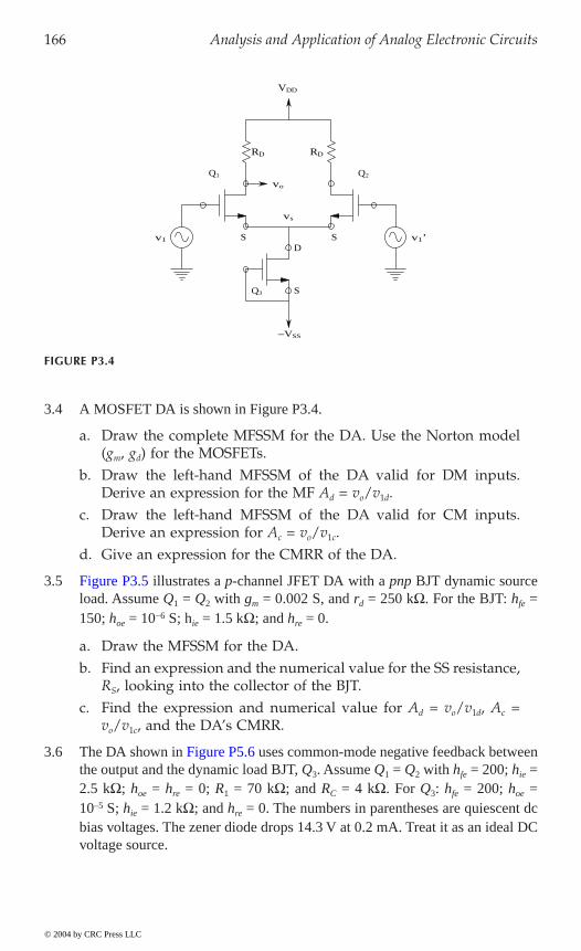
166 Analysis and Application of Analog Electronic Circuits
3.4 A MOSFET DA is shown in Figure P3.4.
a. Draw the complete MFSSM for the DA. Use the Norton model(gm, gd) for the MOSFETs.
b. Draw the left-hand MFSSM of the DA valid for DM inputs.Derive an expression for the MF Ad = vo/v1d.
c. Draw the left-hand MFSSM of the DA valid for CM inputs.Derive an expression for Ac = vo/v1c.
d. Give an expression for the CMRR of the DA.
3.5load. Assume Q1 = Q2 with gm = 0.002 S, and rd = 250 kW. For the BJT: hfe =150; hoe = 10-6 S; hie = 1.5 kW; and hre = 0.
a. Draw the MFSSM for the DA.b. Find an expression and the numerical value for the SS resistance,
RS, looking into the collector of the BJT.c. Find the expression and numerical value for Ad = vo/v1d, Ac =
vo/v1c, and the DA’s CMRR.
3.6the output and the dynamic load BJT, Q3. Assume Q1 = Q2 with hfe = 200; hie =2.5 kW; hoe = hre = 0; R1 = 70 kW; and RC = 4 kW. For Q3: hfe = 200; hoe =10–5 S; hie = 1.2 kW; and hre = 0. The numbers in parentheses are quiescent dcbias voltages. The zener diode drops 14.3 V at 0.2 mA. Treat it as an ideal DCvoltage source.
FIGURE P3.4
−VSS
VDD
RD RD
vs
v1 v1’
vo
S S
S
D
Q1 Q2
Q3
© 2004 by CRC Press LLC
Figure P3.5 illustrates a p-channel JFET DA with a pnp BJT dynamic source
The DA shown in Figure P5.6 uses common-mode negative feedback between
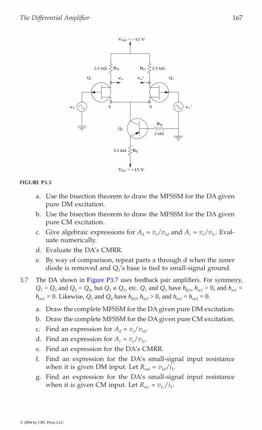
The Differential Amplifier 167
a. Use the bisection theorem to draw the MFSSM for the DA givenpure DM excitation.
b. Use the bisection theorem to draw the MFSSM for the DA givenpure CM excitation.
c. Give algebraic expressions for Ad = vo/v1d and Ac = vo/v1c. Eval-uate numerically.
d. Evaluate the DA’s CMRR.e. By way of comparison, repeat parts a through d when the zener
diode is removed and Q3’s base is tied to small-signal ground.
3.7Q1 = Q3 and Q2 = Q4, but Q1 π Q2, etc. Q1 and Q3 have hfe1, hie1 > 0, and hre1 =hoe1 = 0. Likewise, Q2 and Q4 have hfe2, hie2 > 0, and hre2 = hoe2 = 0.
a. Draw the complete MFSSM for the DA given pure DM excitation.b. Draw the complete MFSSM for the DA given pure CM excitation.c. Find an expression for Ad = vo/v1d.d. Find an expression for Ac = vo/v1c.e. Find an expression for the DA’s CMRR.f. Find an expression for the DA’s small-signal input resistance
when it is given DM input. Let Rind = v1d/i1.g. Find an expression for the DA’s small-signal input resistance
when it is given CM input. Let Rinc = v1c/i1.
FIGURE P3.5
RE3.5 kΩ
RB
2 kΩ
RD RD3.5 kΩ 3.5 kΩ
VEE = +15 V
VDD = −15 V
v1 v1’S S
vo vo’Q1 Q2
Q3
© 2004 by CRC Press LLC
The DA shown in Figure P3.7 uses feedback pair amplifiers. For symmetry,
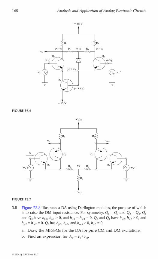
168 Analysis and Application of Analog Electronic Circuits
3.8is to raise the DM input resistance. For symmetry, Q1 = Q3 and Q2 = Q4. Q1
and Q3 have hfe1, hie1 > 0, and hre1 = hoe1 = 0. Q2 and Q4 have hfe2, hie2 > 0, andhre2 = hoe2 = 0. Q5 has hfe5, hie5, and hoe5 > 0, hre5 = 0.
a. Draw the MFSSMs for the DA for pure CM and DM excitations.b. Find an expression for Ad = vo/v1d.
FIGURE P3.6
FIGURE P3.7
(+7 V)(+7 V)
(−14.3 V)
− 15 V
(0 V)
(0 V)(0 V)
(−0.7 V)
R1 R1
+ 15 V
v1 v1’
Q1 Q2
Q3
RC RC
vo
vo vo’
R1 R1
R2 R2
R3
v1’v1
+VEE
−VCC
Q1
Q2 Q4
Q3
i1
v3
© 2004 by CRC Press LLC
Figure P3.8 illustrates a DA using Darlington modules, the purpose of which
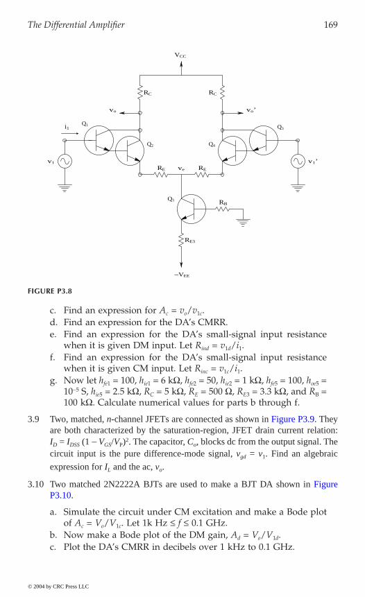
The Differential Amplifier 169
c. Find an expression for Ac = vo/v1c.d. Find an expression for the DA’s CMRR.e. Find an expression for the DA’s small-signal input resistance
when it is given DM input. Let Rind = v1d/i1.f. Find an expression for the DA’s small-signal input resistance
when it is given CM input. Let Rinc = v1c/i1.g. Now let hfe1 = 100, hie1 = 6 kW, hfe2 = 50, hie2 = 1 kW, hfe5 = 100, hoe5 =
10-5 S, hie5 = 2.5 kW, RC = 5 kW, RE = 500 W, RE3 = 3.3 kW, and RB =100 kW. Calculate numerical values for parts b through f.
3.9are both characterized by the saturation-region, JFET drain current relation:ID = IDSS (1 - VGS/VP)2. The capacitor, Co, blocks dc from the output signal. Thecircuit input is the pure difference-mode signal, vgd = v1. Find an algebraic
expression for IL and the ac, vo.
3.10
a. Simulate the circuit under CM excitation and make a Bode plotof Ac = Vo/V1c. Let 1k Hz £ f £ 0.1 GHz.
b. Now make a Bode plot of the DM gain, Ad = Vo/V1d.c. Plot the DA’s CMRR in decibels over 1 kHz to 0.1 GHz.
FIGURE P3.8
Q2 Q4
i1Q1 Q3
v1’v1
RE3
RB
RE RE
RC RC
ve
−VEE
VCC
Q5
vo vo’
© 2004 by CRC Press LLC
Two, matched, n-channel JFETs are connected as shown in Figure P3.9. They
Two matched 2N2222A BJTs are used to make a BJT DA shown in FigureP3.10.

170 Analysis and Application of Analog Electronic Circuits
3.11 E5
RS = 500 W, RC = 6.8 kW, RB = 1 MW; BJTs: hoe = hre = 0; hfe = 100; hie =2.5 kW. Assume Cc is a small-signal short circuit.
a. Use MFSS analysis and the bisection theorem to find numericalvalues for AD, AC, and the CMRR. AD ∫ vo/v1d and AC ∫ vo/v1c.
b. Now the vo output is coupled to a 10-kW load resistance, RL,making the DA circuit asymmetrical, so the bisection theorem nolonger can be used. Repeat a.
3.12 It is desired to measure the CMRR of a student-built differential amplifier (see
FIGURE P3.9
FIGURE P3.10
vo
Co
VDD
+
VGSQ+
v1
−
−
v1 S
Dvg vg’
D
RDIL
ve
vo’vo
1 µF µF
Q1 Q2
v1’v1
1.5 MΩ6 kΩ1.5 MΩ 6 kΩ
5 kΩ
−15 V
15 V
Q1 = Q2 = 2N2222A
© 2004 by CRC Press LLC
A BJT DA is shown in Figure P3.11. The circuit is symmetrical. R = 10 W,
Figure P3.12). First, the two inputs are shorted together and connected to a
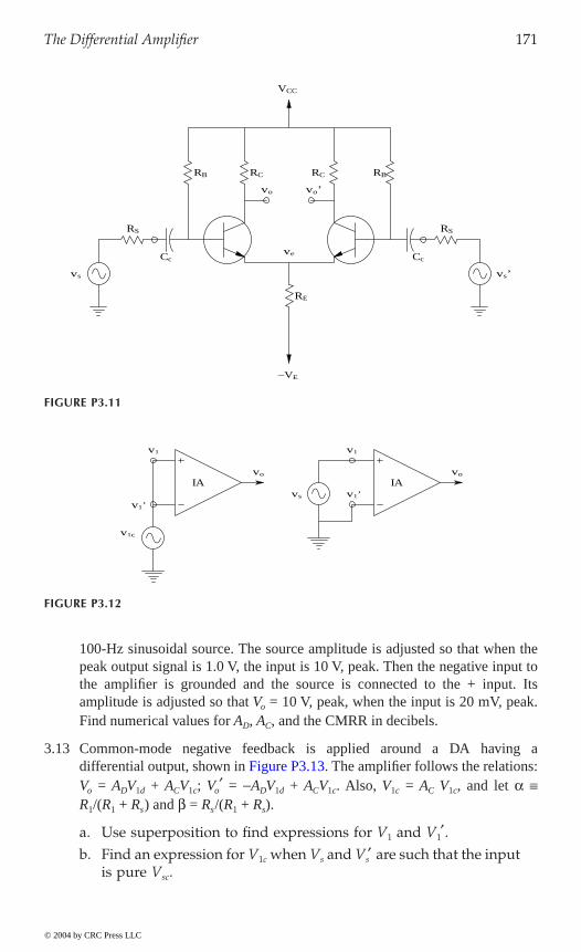
The Differential Amplifier 171
100-Hz sinusoidal source. The source amplitude is adjusted so that when thepeak output signal is 1.0 V, the input is 10 V, peak. Then the negative input tothe amplifier is grounded and the source is connected to the + input. Itsamplitude is adjusted so that Vo = 10 V, peak, when the input is 20 mV, peak.Find numerical values for AD, AC, and the CMRR in decibels.
3.13 Common-mode negative feedback is applied around a DA having a
Vo = ADV1d + ACV1c; Vo¢ = -ADV1d + ACV1c. Also, V1c = AC V1c, and let a ∫R1/(R1 + Rs) and b = Rs/(R1 + Rs).
a. Use superposition to find expressions for V1 and V1¢.b. Find an expression for V1c when Vs and Vs¢ are such that the input
is pure Vsc.
FIGURE P3.11
FIGURE P3.12
RC RCRB RB
RS RS
vo vo’
vs vs’
ve
RE
VCC
−VE
Cc Cc
v1c
vo vo
vs
IA IAv1’
v1v1
v1’
© 2004 by CRC Press LLC
differential output, shown in Figure P3.13. The amplifier follows the relations:

172 Analysis and Application of Analog Electronic Circuits
c. Find an expression for V1d when the input is pure Vsd.d. Find an expression for the CMNF amplifier’s CMRR. Compare
it to the CMRR of the DA alone. Let R1 = R2 = 106 W; Kcm = -103;AC = 1, and AD = 103. Evaluate the system’s CMRR numerically.
FIGURE P3.13
DA
Vo
Vo’
R
R
Vo
Kcm
V1
V1’
R1
R1
Rs
Rs
Vs
Vs’
KcmVoc
© 2004 by CRC Press LLC
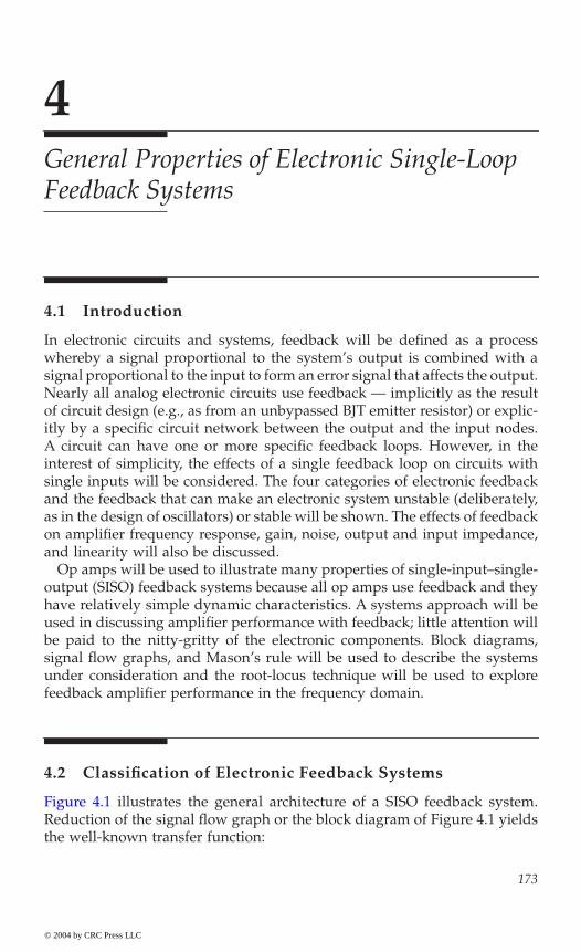
173
4General Properties of Electronic Single-Loop Feedback Systems
4.1 Introduction
In electronic circuits and systems, feedback will be defined as a processwhereby a signal proportional to the system’s output is combined with asignal proportional to the input to form an error signal that affects the output.Nearly all analog electronic circuits use feedback — implicitly as the resultof circuit design (e.g., as from an unbypassed BJT emitter resistor) or explic-itly by a specific circuit network between the output and the input nodes.A circuit can have one or more specific feedback loops. However, in theinterest of simplicity, the effects of a single feedback loop on circuits withsingle inputs will be considered. The four categories of electronic feedbackand the feedback that can make an electronic system unstable (deliberately,as in the design of oscillators) or stable will be shown. The effects of feedbackon amplifier frequency response, gain, noise, output and input impedance,and linearity will also be discussed.
Op amps will be used to illustrate many properties of single-input–single-output (SISO) feedback systems because all op amps use feedback and theyhave relatively simple dynamic characteristics. A systems approach will beused in discussing amplifier performance with feedback; little attention willbe paid to the nitty-gritty of the electronic components. Block diagrams,signal flow graphs, and Mason’s rule will be used to describe the systemsunder consideration and the root-locus technique will be used to explorefeedback amplifier performance in the frequency domain.
4.2 Classification of Electronic Feedback Systems
Reduction of the signal flow graph or the block diagram of Figure 4.1 yieldsthe well-known transfer function:
© 2004 by CRC Press LLC
Figure 4.1 illustrates the general architecture of a SISO feedback system.

174 Analysis and Application of Analog Electronic Circuits
(4.1)
From this simple result, the following important quantities describingfeedback systems can be defined:
• Forward gain = open-loop gain = Kv (4.2A)• Loop gain = AL = Kv (4.2B)• Return difference = RD = 1 - AL (4.2C)• dB of feedback = -20 log 1 - AL (4.2D)
Note that , , Kv, and AL can be scalars or vectors (complex functions offrequency).
A SISO system is said to have negative feedback (NFB) if it has a minussign associated with either Kv, , or the summer, or with all three elementsin the block diagram. Control systems generally use NFB and it is usual toassume a subtraction of Vo at the summer. Electronic systems do not nec-essarily have a subtraction at the summer; it depends on circuit design. Tosee if a SISO electronic feedback system has negative feedback, inspect theloop gain. AL(j0) will have a minus sign (be a negative number) if thefeedback amplifier is a direct-coupled (DC) negative feedback system. If theamplifier is reactively coupled (RC), then AL(jw) will have a minus sign atmid-frequencies (its phase angle will be -180∞). Feedback amplifier is gen-erally a voltage, but VCCSs are encountered. Considering that feedback canhave either sign and the fed-back quantity can be voltage or current, it is
FIGURE 4.1Two alternate representations for a single-input–single-output (SISO) linear feedback system.(A) Signal flow graph notation. (B) Block diagram notation.
Kv
Kv
β
β
αx
yαxe+
+
A
B
VV
KK
o
s
v
v
=-a
b1
© 2004 by CRC Press LLC
General Properties of Electronic Single-Loop Feedback Systems 175
clear that four major types of feedback exist: (1) negative voltage feedback;(2) negative current feedback; (3) positive voltage feedback; and (4) positivecurrent feedback. Negative voltage feedback is most widely encountered inelectronic engineering practice. Its properties will be examined in the fol-lowing sections.
4.3 Some Effects of Negative Voltage Feedback
4.3.1 Reduction of Output Resistance
Figure 4.2 illustrates a simple Thevenin amplifier circuit with NVB appliedto its summing junction (input node). Assume that the amplifier’s inputresistor, Rin, RF and Rs, so Rin can be ignored in writing the node equationfor Vi. Also, in finding the NFB amplifier’s open-circuit voltage gain, assumethat Ro RF, so negligible voltage drop takes place across Ro. Thus, the nodeequation is:
Vi [Gs + GF] - Vo GF = Vs Gs (4.3)
Also,
Vo @ -KvVi (4.4)
Thus:
Vi = -Vo/Kv (4.5)
and
-(Vo/Kv)(Gs + GF) - Vo GF = Vs Gs (4.6)
FIGURE 4.2Schematic of a simple Thevenin VCVS with negative feedback. See text for analysis.
+
RF
Vi Ro VoRs SC
KvViVs RiIoSC
−+
© 2004 by CRC Press LLC
176 Analysis and Application of Analog Electronic Circuits
Thus, Equation 4.6 can be used to write the closed-loop system’s transferfunction:
(4.7)
Note in comparing Equation 4.7 to Equation 4.1, that
AL = -Kv [Rs/(RF + Rs)] (Note: system has NFB.) (4.8)
a = RF/(RF + Rs) (4.9)
b = Rs/(RF + Rs) (4.10)
In op amps, Kv is numerically very large, so Equation 4.7 reduces to thewell-known gain relation for the ideal op amp inverter: Vo/Vs = -RF/Rs.)
There are two common ways to find the output resistance of the simples
test source, Vt, between the Vo node and ground and calculate Rout = Vt/It.The other method is to measure the open-circuit output voltage using Equa-tion 4.7, then calculate the short-circuit output current (with Vo = 0). Clearly,Rout = VOC/IoSC. Inspection of Figure 4.2 with a shorted output lets one write:
(4.11)
Now Rout can be found:
(4.12)
In general, the NFB amplifier’s output impedance can be written as afunction of frequency:
Zout(jw) = Ro/RD(jw) (4.13)
Note that, in general, Zout(jw) is very small (e.g., milliohms) at dc andlow frequencies, then gradually increases with w. This property can be dem-onstrated by assuming Kv to have a frequency response of the form:
(4.14)
VV
K GG G K G
K R R R
K R R RAo
s
v s
s F v F
v F F s
v s F sv=
-+ +
=- +( )
+ +( ) =1
IoSCs
s F
v F
o
s v F
o F s
VR R
K RR
V K RR R R
=+( ) -
È
ÎÍ
ù
ûú @
-+( )1
R
K R R R
K R R RV K R
R R R
RK R R R
RK
RAout
v F F s
v s F s
s v F
o F s
o
v s F s
o
v
o
L
=
- +( )+ +( )
-+( )
=+ +( ) =
+=
-1
1 1 1b
Kv jK
jvow
wt( ) =
+ 1
© 2004 by CRC Press LLC
NFB amplifier of Figure 4.2. One is to set V = 0, then place an independent
General Properties of Electronic Single-Loop Feedback Systems 177
Equation now yields:
(4.15)
From the preceding equation it is clear that Zo @ Ro/bKvo at dc, increasingwith frequency to Zo = Ro at frequencies above bKvo/t r/s.
4.3.2 Reduction of Total Harmonic Distortion
A very important property of NFB is the reduction of total harmonic distor-tion (THD) at the output of amplifiers, in particular power amplifiers. Firstit is necessary to examine what THD means. Assume that a certain amplifierhas a soft saturation nonlinearity modeled by:
y = ax + bx2 + cx3 + dx4 + ex5 +… (4.16)
Clearly, a = Kv, the linear gain. The b, c, d, e, … terms can be zero or haveeither sign. They give rise to the harmonic distortion that can be the resultof transistor cut-off or saturation, or power supply saturation. If x(t) = Xo
sin(wot), the output y(t) will contain the desired fundamental frequency fromthe a-term, as well as unwanted harmonics. For example,
(4.17)
The power terms approximating the nonlinear transfer characteristic ofthe amplifier generate dc, fundamental, and harmonics of the order of thenonlinear term in addition to the desired fundamental frequency. These canbe summarized by the expression:
y(t) = Kv Xo sin(wot) + H2 sin(2wot) + H3 sin(3wot) + H4 sin(4wot) +… (4.18)
The total RMS harmonic distortion is defined as:
(4.19)
Note that Hk2/2 is the mean squared value of the kth harmonic; (Kv
2Xo2/2) is
the MS value of the fundamental frequency (desired) component of theoutput. In general, the larger Xo is, the larger will be the THD.
Zo jR
K jR j
j K
R K j
j Ko
vo
o
vo
o vo
vo
wb wt
wtwt b
b wtwt b
( ) =+ +( ) =
+( )+ +( ) =
+( )[ ] +( )+( ) +1 1
11
1 1
1 1
y t a X t bX t cX
t t
o o o o o
o o
( ) = ( ) + ( ) - ( )[ ] + ( )( ) - ( )[ ] + º
sin cos
sin sin
w w
w w
2 32 1 2 4
3 3
THD = + + + º ==
ÂH H H Hkk
22
32
42 2
2
2 2 2 2
© 2004 by CRC Press LLC
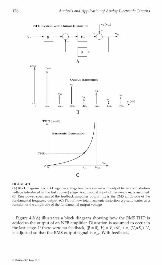
178 Analysis and Application of Analog Electronic Circuits
Figure 4.3(A) illustrates a block diagram showing how the RMS THD isadded to the output of an NFB amplifier. Distortion is assumed to occur inthe last stage. If there were no feedback, (b = 0), Vo = Vs aKv + vd (VsaKv). Vs
is adjusted so that the RMS output signal is vos1. With feedback,
FIGURE 4.3(A) Block diagram of a SISO negative voltage feedback system with output harmonic distortionvoltage introduced in the last (power) stage. A sinusoidal input of frequency wo is assumed.(B) Rms power spectrum of the feedback amplifier output. vos1 is the RMS amplitude of thefundamental frequency output. (C) Plot of how total harmonic distortion typically varies as afunction of the amplitude of the fundamental output voltage.
a
b
KvVs
-
++
Vo
vd (vos)
w (r/s)
rms
00 wo 2wo 3wo 7wo6wo5wo4wo
vos1
vd2
vd
vd
vd
vd
vd
vos
VCLvos00
THD1
THD (rmsV)
B
A
C
Output Harmonics
NFB System with Output Distortion
Harmonic Generation
© 2004 by CRC Press LLC

General Properties of Electronic Single-Loop Feedback Systems 179
(4.20)
With NFB, the output THD is reduced by a factor of 1/(1 + b Kv), giventhat the signal output is the same in the nonfeedback and the feedback cases.This result has vast implications in the design of nearly distortion-free audiopower amplifiers, as well as linear signal conditioning systems in generalthat use op amps. vdk
th RMS harmonic voltage;i.e., vdk = Hk/ . Figure 4.3(C) shows how the RMS THD increases as thesignal output is made larger. At vos = VCL, the level of distortion increasesabruptly because the amplifier begins to saturate and clip the output signalwaveform.
In good low-distortion amplifier design, the input stages are made as linearas possible, and the amplifier is designed so that the output (power) stagesaturates before the input and intermediate gain stages do. This allows theTHD voltage to effectively be added in the last stage, and thus the THD isreduced by a factor of 1/(1 - AL) = 1/RD.
4.3.3 Increase of NFB Amplifier Bandwidth at the Cost of Gain
It is axiomatic in the design of electronic circuit that negative feedback allowsone to extend closed-loop amplifier bandwidth (BW) at the expense of dc ormid-band gain. Another way of looking at the effect of NFB on BW is toobserve that every amplifier is endowed with some gain*bandwidth product(GBWP); as a figure of merit, larger is better. GBWP remains relativelyconstant as feedback is applied, so when NFB reduces gain, it increases BW.The frequency-compensated (FC) op amp makes an excellent example ofGBWP constancy. The open-loop gain of an FC op amp can be given by:
(4.21)
Note that the op amp is a difference amplifier and has a gain*bandwidthproduct:
GBWPoa = Kvo/(2pta) Hertz (4.22)
Now connect the OA as a simple noninverting amplifier, as shown in
Vo = (Vs - bVo)Kvo/(sta + 1) (4.23)
VV K
K
v v
Kos v
v
v
d os
v
os
=+
+ ( )+
ab b
1
1 11
THD
2
VV V
Ks
o
i i
vo
a- ¢=
+t 1
© 2004 by CRC Press LLC
in Figure 4.3(B) is simply the k
Figure 4.4(A). The amplifier’s output is:
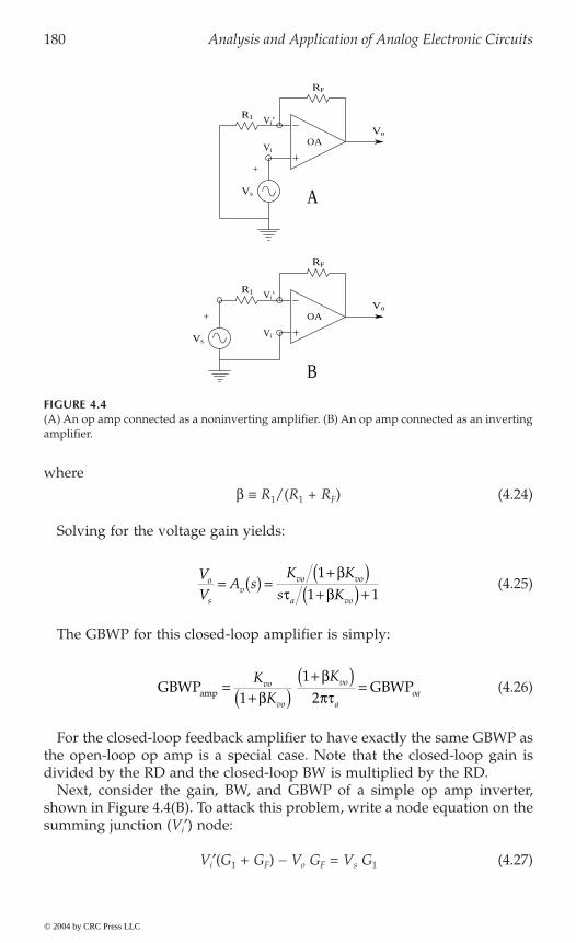
180 Analysis and Application of Analog Electronic Circuits
whereb ∫ R1/(R1 + RF) (4.24)
Solving for the voltage gain yields:
(4.25)
The GBWP for this closed-loop amplifier is simply:
(4.26)
For the closed-loop feedback amplifier to have exactly the same GBWP asthe open-loop op amp is a special case. Note that the closed-loop gain isdivided by the RD and the closed-loop BW is multiplied by the RD.
Next, consider the gain, BW, and GBWP of a simple op amp inverter,shown in Figure 4.4(B). To attack this problem, write a node equation on thesumming junction (Vi¢) node:
Vi¢(G1 + GF) - Vo GF = Vs G1 (4.27)
FIGURE 4.4(A) An op amp connected as a noninverting amplifier. (B) An op amp connected as an invertingamplifier.
Vs
+
RF
Vo
OA
R1 Vi’
RF
Vi’R1
Vs
+ OA
A
B
Vo
Vi
Vi
VV
A sK K
s Ko
sv
vo vo
a vo
= ( ) =+( )
+( ) +1
1 1b
t b
GBWP GBWPamp =+( )
+( ) =K
K
Kvo
vo
vo
aoa1
12b
bpt
© 2004 by CRC Press LLC
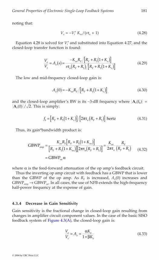
General Properties of Electronic Single-Loop Feedback Systems 181
noting that:
Vo = -Vi¢ Kvo/(sta + 1) (4.28)
Equation 4.28 is solved for Vi¢ and substituted into Equation 4.27, and theclosed-loop transfer function is found:
(4.29)
The low and mid-frequency closed-loop gain is:
(4.30)
and the closed-loop amplifier’s BW is its -3-dB frequency where Av(fb) =Av(0) / . This is simply:
(4.31)
Thus, its gain*bandwidth product is:
(4.32)
where a is the feed-forward attenuation of the op amp’s feedback circuit. Thus the inverting op amp circuit with feedback has a GBWP that is lower
than the GBWP of the op amp. As RF is increased, Av(0) increases andGBWPamp Æ GBWPoa. In all cases, the use of NFB extends the high-frequencyhalf-power frequency at the expense of gain.
4.3.4 Decrease in Gain Sensitivity
Gain sensitivity is the fractional change in closed-loop gain resulting fromchanges in amplifier circuit component values. In the case of the basic SISO
(4.33)
VV
A sK R R R K
s R R R R Ko
sv
vo F F v
a F F v
= ( ) =- + +( )[ ]
+( ) + +( )[ ]1
1 1
1
1t
A K R R R Kv vo F F v0 11( ) = - + +( )[ ]
2
f R R K R Rb F v a F= + +( )[ ] +( )[ ]1 11 2pt hertz
GBWP
GBWP
ampvo F F vo
F vo a F
vo
a
F
F
oa
K R R R K
R R K R R
K RR R
=+ +( )[ ]
+ +( )[ ] +( )[ ] =+( )
=
1
1 1 1
1
1 2 2pt pt
a
VV
AK
Ko
sv
v
v
= =+a
b1
© 2004 by CRC Press LLC
feedback system of Figure 4.3(A), the closed-loop gain is:
182 Analysis and Application of Analog Electronic Circuits
The sensitivity of Av with respect to the gain Kv is defined by:
(4.34)
so now
(4.35)
and the partial derivative is:
(4.36)
Thus,
(4.37)
and the sensitivity is:
(4.38)
In op amps, 1/[RD] is on the order of 10-4 to 10-6, so a circuit with NFB isgenerally quite insensitive to variations in its dc open-loop gain, Kvo.
Also of interest is how sensitivity varies as a function of frequency in NFBcircuits. According to Northrop (1990),
Complex algebra must be used in the calculation of such sensitivities,because the closed-loop gain [frequency response] is complex. Here weexpress the closed-loop gain in polar form for convenience:
Av(jw) = ΩAv(jw)Ω ejq(w) (4.39)
The gain sensitivity, given by Equation [4.38], can also be written as
(4.40)
SA AK KK
A v v
v vv
v ∫DD
D DAAK
Kvv
vv=
∂∂
ÊËÁ
∂∂
=+( ) -[ ]
+( )=
+( )-A
K
K K
K
KK
Kv
v
v v
v
v
v
va b b
ba
b1
1 12
1
RD
DD
AA KKv
v v
v
= [ ]RD
SA AK K
A K AK K KK
A v v
v v
v v v
v v vv
v ∫ = [ ] = [ ]DD
DDRD RD
1
Sd
dx x
d
d xxA v v vv = = ( )
( )A A Aln
ln
© 2004 by CRC Press LLC
General Properties of Electronic Single-Loop Feedback Systems 183
where x is a parameter in the NFB circuit. From Equation [4.39] we canwrite:
(4.41)
Substitution of Equation [4.41] into Equation [4.40] yields:
(4.42)
The real part of SxAv is called the magnitude sensitivity; the imaginary part
of SxAv is the phase sensitivity. Generally, x will be a real number, which
simplifies the calculation of Equation [4.42]. Sensitivity analysis usingEquation [4.42] can be utilized to evaluate active filter designs.
4.4 Effects of Negative Current Feedback
The purpose of negative current feedback (NCF) is to create an approxima-tion to a voltage-controlled current source (VCCS) so that the output current,IL, is proportional to Vs, regardless of the load, which can be nonlinear. InNCF amplifiers, the signal fed back is proportional to the current throughthe load. NCF, like NVF, extends the bandwidth of the amplifier within thefeedback loop. Unlike NVF, NCF raises the output resistance of the amplifier
will be investigated; frequency dependence will not be treated in this exam-ple. A VCCS is characterized by a transconductance, GM, and a Norton shuntconductance, Go.
First, it is necessary to find the circuit’s GM = IL/Vs. Note that the currentis given by Ohm’s law:
(4.43)
The summing junction node voltage is found:
(4.44)
Ø
(4.45)
ln lnA Av vj j jw w q w( )[ ] = ( ) + ( )
Sd j
dx xj
ddx xx
A vv =
( )( )+ ( )ln A w q w
IV K
R R RLi vo
o L c
= ¢+ +
¢ +[ ] - -( ) =V G G I R G G Vi F L c F s1 1
¢ =-
+V
G V I R GG Gis L c F
F
1
1
© 2004 by CRC Press LLC
within the loop. A single op amp circuit with NCF, illustrated in Figure 4.5,
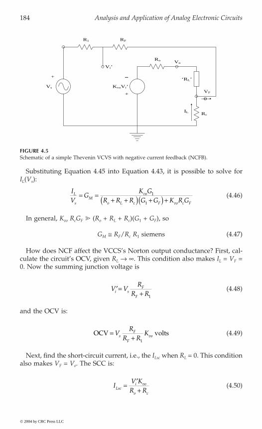
184 Analysis and Application of Analog Electronic Circuits
Substituting Equation 4.45 into Equation 4.43, it is possible to solve forIL(Vs):
(4.46)
In general, Kvo RcGF (Ro + RL + Rc)(G1 + GF), so
GM @ RF/Rc R1 siemens (4.47)
How does NCF affect the VCCS’s Norton output conductance? First, cal-culate the circuit’s OCV, given RL Æ . This condition also makes IL = VF =0. Now the summing junction voltage is
(4.48)
and the OCV is:
(4.49)
Next, find the short-circuit current, i.e., the ILsc when RL = 0. This conditionalso makes VF = Vo. The SCC is:
(4.50)
FIGURE 4.5Schematic of a simple Thevenin VCVS with negative current feedback (NCFB).
KvoVi’
Vi’
R1 RF
VF
Vo
‘RL’
IL
+
+
Vs
Ro
0
Rc
-
IV
GK G
R R R G G K R GL
sM
vo
o L c F vo c F
= =+ +( ) +( ) +
1
1
¢ =+
V VR
R Ri sF
F 1
OCV volts=+
VR
R RKs
F
Fvo
1
IV KR RLsc
i vo
o c
= ¢+
© 2004 by CRC Press LLC
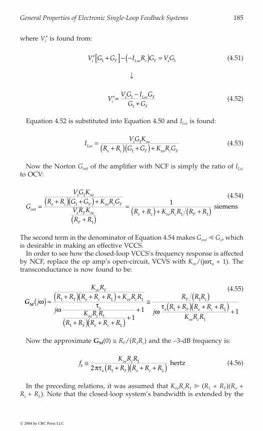
General Properties of Electronic Single-Loop Feedback Systems 185
where Vi¢ is found from:
(4.51)
Ø
(4.52)
Equation 4.52 is substituted into Equation 4.50 and ILsc is found:
(4.53)
Now the Norton Gout of the amplifier with NCF is simply the ratio of ILsc
to OCV:
The second term in the denominator of Equation 4.54 makes Gout Go, whichis desirable in making an effective VCCS.
In order to see how the closed-loop VCCS’s frequency response is affectedby NCF, replace the op amp’s open-circuit, VCVS with Kvo/(jwta + 1). Thetransconductance is now found to be:
Now the approximate GM(0) @ RF/(R1Rc) and the -3-dB frequency is:
(4.56)
In the preceding relations, it was assumed that KvoRcR1 (R1 + RF)(Ro +Rc + RL). Note that the closed-loop system’s bandwidth is extended by the
¢ +[ ] - -( ) =V G G I R G V Gi F Lso c F s1 1
¢ =-+
VV G I G
G Gis Lsc F
F
1
1
IV G K
R R G G K R GLscs vo
o c F vo c F
=+( ) +( ) +
1
1
G
V G KR R G G K R G
V R KR R
R R K R R R Rout
s vo
o c V vo c F
s F vo
F
o c vo c F
=+( ) +( ) +
+( )=
+( ) + +( )
1
1
1
1 1
1 siemens
(4.54)
GM j
K RR R R R R K R R
j K R RR R R R R
R R R
jR R R R R
K R R
vo F
F o c L vo c
a
vo c
F o c L
F c
a F o c L
vo c
ww
tw
t( ) =
+( ) + +( ) +
+( ) + +( ) ++
@ ( )+( ) + +( ) +
1 1
1
1
1
1
111 1
(4.55)
fK R R
R R R R Rbvo c
a F o c L
@+( ) + +( )
1
12 pt hertz
© 2004 by CRC Press LLC
186 Analysis and Application of Analog Electronic Circuits
of having the RL “floating” between Vo and Rc. Also, the peak current islimited by the op amp used.
effective VCCS using NCF can be made from three op amps. The op ampthat drives RL can be made a power op amp and the load can be grounded.Figure 4.6 illustrates this NCF circuit. As in the earlier example, we will findthe VCCS’s GM(jw) and Zout(jw). Because the two feedback amplifiers areunity gain, they have -3-dB frequencies approaching their op amp’s fT andthus can be treated as pure gains (+1 and -1, respectively). The node equationfor the summing junction is written:
Vi¢ [3G] - VoG - (-VL)G = VsG (4.57)
Two auxiliary equations are used:
Vo = - IL (RF + “RL”) (4.58)
(4.59)
Substituting the preceding equations into Equation 4.57 and rearrangingterms yields:
(4.60)
FIGURE 4.6A three-op amp VCCS in which the load is grounded. Analysis is in the text.
V2
R
R
POA
−VL VL
(VCCS)R
VL
0RL
Vo
RF(0) IL
RVs
R
+
Vs
¢ = -+( )
VV j
Kio a
vo
wt 1
IV
GL
sM= ( ) =
+( ) ++( )
+( ) ++
j
KR R K R
jR R
R R K R
vo
F L vo F
a F L
F L vo F
ww
t3
33
1
© 2004 by CRC Press LLC
NCF. The NVF circuit of Figure 4.5 is simple, but suffers the disadvantage
In Section 2.6.7 on laser diodes in Chapter 2, it was determined that an

General Properties of Electronic Single-Loop Feedback Systems 187
In practical cases, Kvo RF 3(RF + RL), so the VCCS’s transconductance canbe approximated as:
(4.61)
Thus, it is clear that GM(0) @ GF and the break frequency is:
(4.62)
which is certainly greater than the op amp’s fT.The VCCS’s Zout(jw) is now of interest. Ideally, it should approach infinity.
To find it, take the ratio of the circuit’s OCV to SCC. Under OCV conditions,IL = 0 and VL = Vo. Using the node equation for Vi¢, it is easy to write:
(4.63)
Next, find the VCCS’s SCC. Under SCC conditions, RL = 0 and VL = 0. Thenode equation for Vi¢ yields:
(4.64)
From Equation 4.64 it can be seen that, at low frequencies, Zout(0) = RFKvo/3.At frequencies above Kvo/3ta r/s, Zout(hi) @ RF, which is not very high, makinga poor VCCS at high frequencies.
4.5 Positive Voltage Feedback
4.5.1 Introduction
Positive voltage feedback (PVF) is seldom used in SISO feedback amplifiers.PVF increases the closed-loop gain, decreases the closed-loop bandwidth,increases the Rout of the system, and increases harmonic distortion at a givenoutput level. These activities are based on the fact that the loop gain in asimple SISO feedback amplifier with PVF is AL = +bKv, so for +bKv < 1, thereturn difference, (1 – AL), is <1. PVF can be used deliberately to make afeed-back system unstable so that it oscillates. The next section illustrates
GM jG
j R R K RF
a F L vo F
wwt
( ) @+( ) ( ) +3 1
fK R
R Rbvo F
a F L
@+( )2 3pt
OCV =-
+( )V K
js vo
a3 1wt
ZoutF vo a vo
a
F vo a vo
a
jR K j K
j
R K j K
jw
w twt
w twt
( ) =+( ) +( ) +[ ]
+( ) @+[ ]
+( )3 3 3 1
3 13 1
3 1
© 2004 by CRC Press LLC
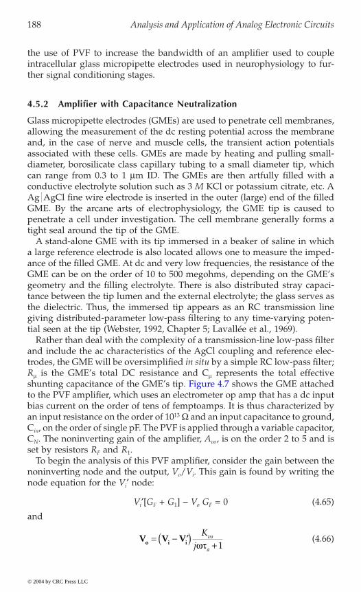
188 Analysis and Application of Analog Electronic Circuits
the use of PVF to increase the bandwidth of an amplifier used to coupleintracellular glass micropipette electrodes used in neurophysiology to fur-ther signal conditioning stages.
4.5.2 Amplifier with Capacitance Neutralization
Glass micropipette electrodes (GMEs) are used to penetrate cell membranes,allowing the measurement of the dc resting potential across the membraneand, in the case of nerve and muscle cells, the transient action potentialsassociated with these cells. GMEs are made by heating and pulling small-diameter, borosilicate class capillary tubing to a small diameter tip, whichcan range from 0.3 to 1 mm ID. The GMEs are then artfully filled with aconductive electrolyte solution such as 3 M KCl or potassium citrate, etc. AAg AgCl fine wire electrode is inserted in the outer (large) end of the filledGME. By the arcane arts of electrophysiology, the GME tip is caused topenetrate a cell under investigation. The cell membrane generally forms atight seal around the tip of the GME.
A stand-alone GME with its tip immersed in a beaker of saline in whicha large reference electrode is also located allows one to measure the imped-ance of the filled GME. At dc and very low frequencies, the resistance of theGME can be on the order of 10 to 500 megohms, depending on the GME’sgeometry and the filling electrolyte. There is also distributed stray capaci-tance between the tip lumen and the external electrolyte; the glass serves asthe dielectric. Thus, the immersed tip appears as an RC transmission linegiving distributed-parameter low-pass filtering to any time-varying poten-tial seen at the tip (Webster, 1992, Chapter 5; Lavallée et al., 1969).
Rather than deal with the complexity of a transmission-line low-pass filterand include the ac characteristics of the AgCl coupling and reference elec-trodes, the GME will be oversimplified in situ by a simple RC low-pass filter;Rm is the GME’s total DC resistance and Cm represents the total effective
to the PVF amplifier, which uses an electrometer op amp that has a dc inputbias current on the order of tens of femptoamps. It is thus characterized byan input resistance on the order of 1013 W and an input capacitance to ground,Cin, on the order of single pF. The PVF is applied through a variable capacitor,CN. The noninverting gain of the amplifier, Avo, is on the order 2 to 5 and isset by resistors RF and R1.
To begin the analysis of this PVF amplifier, consider the gain between thenoninverting node and the output, Vo/Vi. This gain is found by writing thenode equation for the Vi¢ node:
Vi¢[GF + G1] - Vo GF = 0 (4.65)
and
(4.66)V V Vo i i= - ¢( ) +K
jvo
awt 1
© 2004 by CRC Press LLC
shunting capacitance of the GME’s tip. Figure 4.7 shows the GME attached
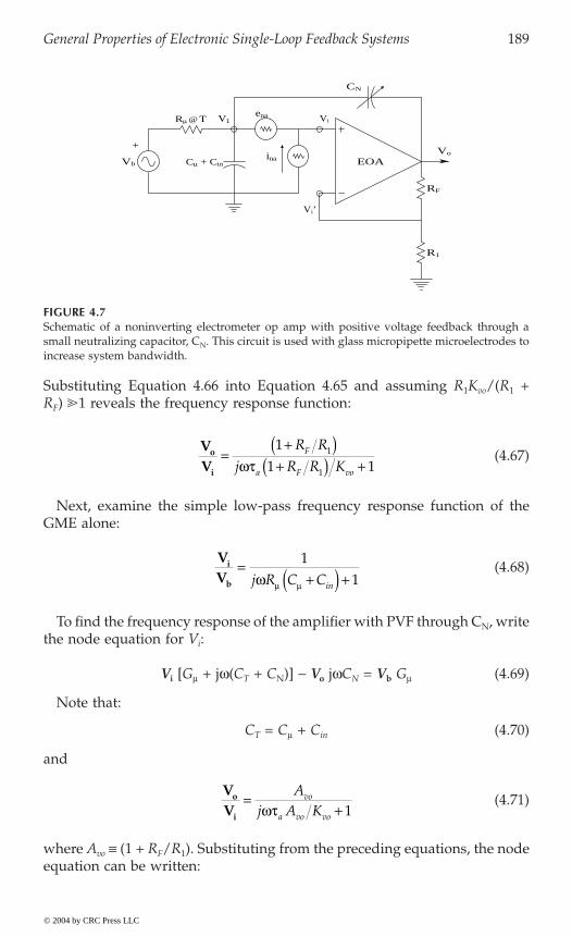
General Properties of Electronic Single-Loop Feedback Systems 189
Substituting Equation 4.66 into Equation 4.65 and assuming R1Kvo/(R1 +RF) 1 reveals the frequency response function:
(4.67)
Next, examine the simple low-pass frequency response function of theGME alone:
(4.68)
To find the frequency response of the amplifier with PVF through CN, writethe node equation for Vi:
Vi [Gm + jw(CT + CN)] - Vo jwCN = Vb Gm (4.69)
Note that:
CT = Cm + Cin (4.70)
and
(4.71)
where Avo ∫ (1 + RF/R1). Substituting from the preceding equations, the nodeequation can be written:
FIGURE 4.7Schematic of a noninverting electrometer op amp with positive voltage feedback through asmall neutralizing capacitor, CN. This circuit is used with glass micropipette microelectrodes toincrease system bandwidth.
RF
R1
Vi’
EOA
CN
Vo
Vi
+
Rµ @ T V1ena
Vb Cµ + Cinina
VV
o
i
=+( )
+( ) +1
1 11
1
R R
j R R KF
a F vowt
VV
i
b
=+( ) +
11j R C Cinw m m
VV
o
i
=+
Aj A K
vo
a vo vowt 1
© 2004 by CRC Press LLC

190 Analysis and Application of Analog Electronic Circuits
(4.72)
Equation 4.72 can be wrestled algebraically into the transfer function ofthe capacitance-neutralized GME amplifier:
From the standard quadratic form, the closed-loop amplifier’s undampednatural frequency squared is:
(4.74)
The amplifier’s damping factor is found from the second term in thedenominator of Equation 4.73
(4.75)
It is now useful to illustrate how the capacitance-neutralized, PVF ampli-fier works with typical numbers. Let Kvo = 105; ta = 10-2 sec; Avo = 2; Rm =108 W; CT = 3.05 pF; and CN = 2.95 pF. From these numbers it can be foundthat wn = 9.129 ¥ 104 r/s, and x = 0.464 (an underdamped second-order systemwith good transient response). Note that if CN = CT, the system is highlyunderdamped and, if CN is slightly greater than CT, the amplifier’s closed-loop poles lie in the right-half s-plane, making the amplifier oscillate. Theprice paid for extending the system’s bandwidth can be shown to be excess
4.6 Chapter Summary
Most electronic amplifiers use negative voltage feedback (NVF), which:
1. Reduces mid-band gain2. Reduces total harmonic distortion at the output at a given signal
output power level3. Reduces Zout at low and mid-frequencies4. Decreases gain sensitivity to certain circuit parameters
V V Vo o b
j A K
AG j C C j C Ga vo vo
voT N N
wtw wm m
+( ) + +( )[ ] - =1
VV
o
b
=( ) +( ) + + - -( )[ ] +
A
j A C C R K j A K R C R C Avo
a vo T N vo a vo vo T N vow t w tm m m2
1 1
(4.73)
wt m
nvo
a vo T N
KA C C R
2 2=+( ) ( ) r s
x w t m m= ( ) + - -( )[ ]n a vo vo T N voA K R C R C A2 1
© 2004 by CRC Press LLC
noise (see Section 9.8.4 in Chapter 9).
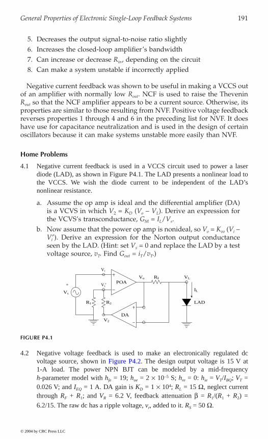
General Properties of Electronic Single-Loop Feedback Systems 191
5. Decreases the output signal-to-noise ratio slightly6. Increases the closed-loop amplifier’s bandwidth7. Can increase or decrease Rin, depending on the circuit8. Can make a system unstable if incorrectly applied
Negative current feedback was shown to be useful in making a VCCS outof an amplifier with normally low Rout. NCF is used to raise the TheveninRout so that the NCF amplifier appears to be a current source. Otherwise, itsproperties are similar to those resulting from NVF. Positive voltage feedbackreverses properties 1 through 4 and 6 in the preceding list for NVF. It doeshave use for capacitance neutralization and is used in the design of certainoscillators because it can make systems unstable more easily than NVF.
Home Problems
4.1 Negative current feedback is used in a VCCS circuit used to power a laserdiode (LAD), as shown in Figure P4.1. The LAD presents a nonlinear load tothe VCCS. We wish the diode current to be independent of the LAD’snonlinear resistance.
a. Assume the op amp is ideal and the differential amplifier (DA)is a VCVS in which V2 = KD (Vo - VL). Derive an expression forthe VCVS’s transconductance, GM = IL/Vs.
b. Now assume that the power op amp is nonideal, so Vo = Kvo (Vi -Vi¢). Derive an expression for the Norton output conductanceseen by the LAD. (Hint: set Vs = 0 and replace the LAD by a testvoltage source, vT. Find Gout = iT/vT.)
4.2 Negative voltage feedback is used to make an electronically regulated dc
1-A load. The power NPN BJT can be modeled by a mid-frequencyh-parameter model with hfe = 19; hoe = 2 ¥ 10-5 S; hre = 0: hie = VT/IBQ; VT =0.026 V; and IEQ = 1 A. DA gain is KD = 1 ¥ 104; RL = 15 W, neglect currentthrough RF + R1; and VR = 6.2 V, feedback attenuation b = R1/(R1 + R2) =
6.2/15. The raw dc has a ripple voltage, vr, added to it. RS = 50 W.
FIGURE P4.1
POA
DA
RF
IL
LAD
VLVo
R2R1
Vs
Vi
Vi’+
V2
© 2004 by CRC Press LLC
voltage source, shown in Figure P4.2. The design output voltage is 15 V at
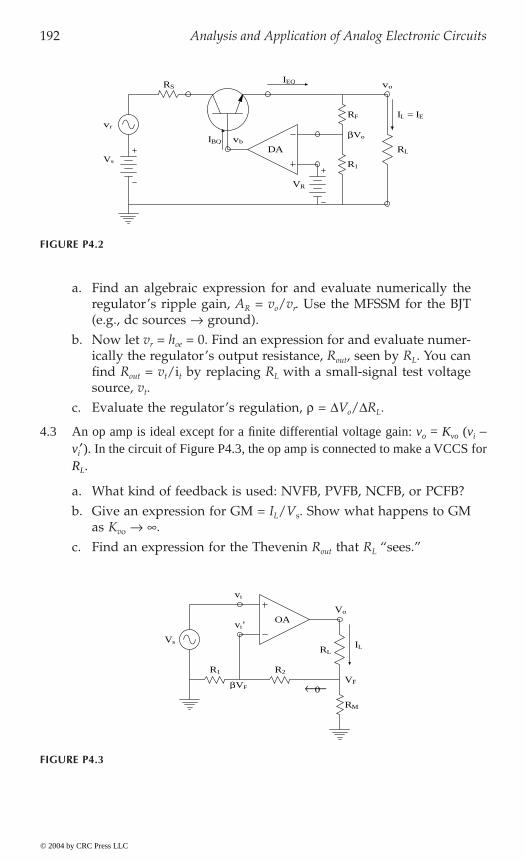
192 Analysis and Application of Analog Electronic Circuits
a. Find an algebraic expression for and evaluate numerically theregulator’s ripple gain, AR = vo/vr. Use the MFSSM for the BJT(e.g., dc sources Æ ground).
b. Now let vr = hoe = 0. Find an expression for and evaluate numer-ically the regulator’s output resistance, Rout, seen by RL. You canfind Rout = vt/it by replacing RL with a small-signal test voltagesource, vt.
c. Evaluate the regulator’s regulation, r = DVo/DRL.
4.3 An op amp is ideal except for a finite differential voltage gain: vo = Kvo (vi -vi¢). In the circuit of Figure P4.3, the op amp is connected to make a VCCS forRL.
a. What kind of feedback is used: NVFB, PVFB, NCFB, or PCFB?b. Give an expression for GM = IL/Vs. Show what happens to GM
as Kvo Æ .c. Find an expression for the Thevenin Rout that RL “sees.”
FIGURE P4.2
FIGURE P4.3
vr
Vs
VR
DA
R1
βVo
RF IL = IE
RL
IBQ vb
IEQRS vo
RL
RM
Vo
VF
R1 R2
vi
vi’
Vs
OA
←βVF 0
IL
© 2004 by CRC Press LLC
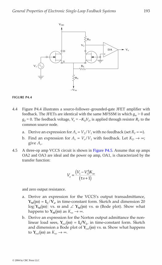
General Properties of Electronic Single-Loop Feedback Systems 193
4.4 Figure P4.4 illustrates a source-follower–grounded-gate JFET amplifier withfeedback. The JFETs are identical with the same MFSSM in which gm > 0 andgd = 0. The feedback voltage, Vo = -KDV2, is applied through resistor RF to thecommon source node.
a. Derive an expression for Av = V2/V1 with no feedback (set RF = ).b. Find an expression for Av = Vo/V1 with feedback. Let KD Æ ;
give Av.
4.5OA2 and OA3 are ideal and the power op amp, OA1, is characterized by thetransfer function:
and zero output resistance.
a. Derive an expression for the VCCS’s output transadmittance,YM(jw) = IL/Vs, in time-constant form. Sketch and dimension 20log YM(jw) vs. w and YM(jw) vs. w (Bode plot). Show whathappens to YM(jw) as Kvo Æ .
b. Derive an expression for the Norton output admittance the non-linear load sees, Yout(jw) = IL/VL, in time-constant form. Sketchand dimension a Bode plot of Yout(jw) vs. w. Show what happensto Yout(jw) as Kvo Æ .
FIGURE P4.4
RS
RF
RD
DA
V2
V1
S
VoD
VDD
−VSS
VV V K
sovo=
- ¢( )+( )
1 1
1t
© 2004 by CRC Press LLC
A three-op amp VCCS circuit is shown in Figure P4.5. Assume that op amps
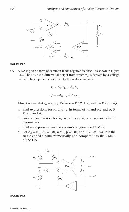
194 Analysis and Application of Analog Electronic Circuits
4.6 A DA is given a form of common-mode negative feedback, as shown in FigureP4.6. The DA has a differential output from which voc is derived by a voltagedivider. The amplifier is described by the scalar equations:
vo = AD v1c + AC v1c
vo¢ = -AD v1c + AC v1c
Also, it is clear that voc = AC v1c. Define a = R1/(R1 + Rs) and b = Rs/(R1 + Rs).
a. Find expressions for v1c and v1d in terms of vsc and vsd, and a, b,K, AD, and AC.
b. Give an expression for vo in terms of vsc and vsd and circuitparameters.
c. Find an expression for the system’s single-ended CMRR.d. Let AD = 100; AC = 0.01; a @ 1; b = 0.01; and K = 104. Evaluate the
single-ended CMRR numerically and compare it to the CMRRof the DA.
FIGURE P4.5
FIGURE P4.6
IOAIOA
POARF
RL
−VL
R R
R
R
IL
VL
VL
Vo
Vs
V1
V1’
R1
R
RRS
vo’
vo
vocDA
−K
RS
R1vs
vs’
v1’
v1
© 2004 by CRC Press LLC
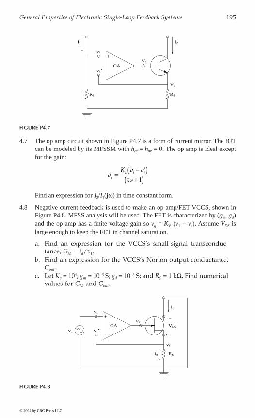
General Properties of Electronic Single-Loop Feedback Systems 195
4.7 The op amp circuit shown in Figure P4.7 is a form of current mirror. The BJTcan be modeled by its MFSSM with hre = hoe = 0. The op amp is ideal exceptfor the gain:
Find an expression for I2/I1(jw) in time constant form.
4.8 Negative current feedback is used to make an op amp/FET VCCS, shown inFigure P4.8. MFSS analysis will be used. The FET is characterized by (gm, gd)and the op amp has a finite voltage gain so vg = KV (v1 - vs). Assume VDS islarge enough to keep the FET in channel saturation.
a. Find an expression for the VCCS’s small-signal transconduc-tance, GM = id/v1.
b. Find an expression for the VCCS’s Norton output conductance,Gout.
c. Let Kv = 104; gm = 10-3 S; gd = 10-5 S; and RS = 1 kW. Find numericalvalues for GM and Gout.
FIGURE P4.7
FIGURE P4.8
I1 I2
R1 R2
V1
vi’
vi
OA
Ve
vK v v
sov i i=
- ¢( )+( )t 1
vi’
vi
OA
RS
vs
v1
id
S
VDS
vg+
id
© 2004 by CRC Press LLC

196 Analysis and Application of Analog Electronic Circuits
4.9 A certain power op amp (POA) has an open-loop gain of Vo/Vi¢ = - 5 ¥ 104.When it is connected as a gain of -250 amplifier, it has a total harmonicdistortion (THD) of 0.5% of the RMS fundamental output signal voltage, Vos,when the RMS Vos = 10.0 V. Find the percent THD when the amplifier is given again of -1 (unit inverter) and the Vos is again made 10.0 VRMS. See Figure P4.9.
4.10 The circuit of Figure P4.10 is a constant-current regulator used for chargingbatteries; NCFB is used. Assume the DA’s gain is KD = 105; hoe = hre = 0; hfe =19; Rm = 1.0 W; VR = 5 V (sets IL); and VBE = 0.7 V. Battery: VB = 12.6 V(nominal); series resistance (nominal); RB = 0.1 W; VS = 24 V; and RS = 13 W.
a. Find an expression for and evaluate numerically the small-signaltransconductance of the regulator, GM = IL/VR.
b. Find an expression for and evaluate numerically the small-signalNorton conductance the battery sees. (Hint: set VR = 0 and use atest source, vt, in place of the battery. Gout = it/vt.)
FIGURE P4.9
FIGURE P4.10
RF
R1
RL10 Ω
Vo
V1
OAVi’
DA
IL
VB
RB
Vo
Vm
Rm
VR
Vb
IB
RS
VS
VBE
−
+ B attery
© 2004 by CRC Press LLC
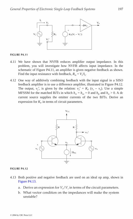
General Properties of Electronic Single-Loop Feedback Systems 197
4.11 We have shown that NVFB reduces amplifier output impedance. In thisproblem, you will investigate how NVFB affects input impedance. In theschematic of Figure P4.11, an amplifier is given negative feedback as shown.Find the input resistance with feedback, Rin = Vs/Is.
4.12 One way of additively combining feedback with the input signal in a SISOfeedback amplifier is to use a difference amplifier, illustrated in Figure P4.12.The output, v2¢, is given by the relation: v2¢ = KF (vs - vo). Use a simpleMFSSM for the matched BJTs in which hre = hoe = 0 and hfe and hie > 0. A dccurrent source supplies the emitter currents of the two BJTs. Derive anexpression for KF in terms of circuit parameters.
4.13 Both positive and negative feedback are used on an ideal op amp, shown in
a. Derive an expression for Vo/Vs in terms of the circuit parameters.b. What vector condition on the impedances will make the system
unstable?
FIGURE P4.11
FIGURE P4.12
K1(Vi − Vi’)
Vo
R1Vs
Vi’
−βK2
Vi
Is
+
vovs
ve
v2’
R R
2IEQ
+ +
VCC
© 2004 by CRC Press LLC
Figure P4.13.

198 Analysis and Application of Analog Electronic Circuits
FIGURE P4.13
vs
IOA vo
Z1 Z2
Z3
Z4
vi
vi’
© 2004 by CRC Press LLC

199
5Feedback, Frequency Response, and Amplifier Stability
5.1 Introduction
This chapter explains the details of how feedback changes open-loop amplifierfrequency response and examines how NVF and PVF can lead to amplifierinstability. Practical use can be made of instability; tunable sinusoidal oscil-lators can be designed using the same analytical techniques used in thedesign of linear feedback amplifiers.
Over the years, many analytical techniques have been used to analyze anddesign feedback systems. In the author’s opinion, the root-locus techniqueis one of the more useful ones. It allows the s-plane location of the closed-loop (CL) system’s poles to be found, given the system’s dc or mid-frequencyloop gain and the location of the poles and zeros of the system’s loop gain,AL(s). Once the closed-loop poles and zeros are known, it is a simple matterto find the CL system’s frequency response or its output in time, given atransient input.
5.2 Review of Amplifier Frequency Response
5.2.1 Introduction
The steady-state sinusoidal frequency response has long been a performancecriterion for linear signal conditioning systems. For example, an amplifier isgiven a continuous sinusoidal input of known frequency and an amplitudethat does not saturate the amplifier. At the output, a sinusoidal output ofthe same frequency, but generally with a different amplitude from the input,and a phase shifted from the input sinusoid can be measured. The amplitudeand phase shift of the output are frequency dependent. The frequencyresponse measured experimentally can be used to define the frequencyresponse function of the amplifier. This is the 2-D vector, H(jw). In polar form:
© 2004 by CRC Press LLC
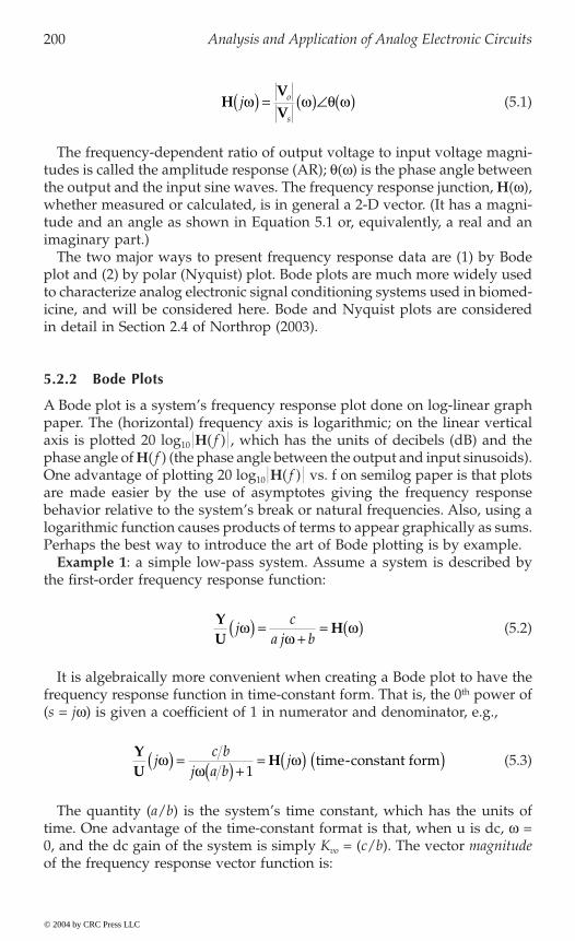
200 Analysis and Application of Analog Electronic Circuits
(5.1)
The frequency-dependent ratio of output voltage to input voltage magni-tudes is called the amplitude response (AR); q(w) is the phase angle betweenthe output and the input sine waves. The frequency response junction, H(w),whether measured or calculated, is in general a 2-D vector. (It has a magni-tude and an angle as shown in Equation 5.1 or, equivalently, a real and animaginary part.)
The two major ways to present frequency response data are (1) by Bodeplot and (2) by polar (Nyquist) plot. Bode plots are much more widely usedto characterize analog electronic signal conditioning systems used in biomed-icine, and will be considered here. Bode and Nyquist plots are consideredin detail in Section 2.4 of Northrop (2003).
5.2.2 Bode Plots
A Bode plot is a system’s frequency response plot done on log-linear graphpaper. The (horizontal) frequency axis is logarithmic; on the linear verticalaxis is plotted 20 log10 H( f ) , which has the units of decibels (dB) and thephase angle of H( f ) (the phase angle between the output and input sinusoids).One advantage of plotting 20 log10 H( f ) vs. f on semilog paper is that plotsare made easier by the use of asymptotes giving the frequency responsebehavior relative to the system’s break or natural frequencies. Also, using alogarithmic function causes products of terms to appear graphically as sums.Perhaps the best way to introduce the art of Bode plotting is by example.
Example 1: a simple low-pass system. Assume a system is described bythe first-order frequency response function:
(5.2)
It is algebraically more convenient when creating a Bode plot to have thefrequency response function in time-constant form. That is, the 0th power of(s = jw) is given a coefficient of 1 in numerator and denominator, e.g.,
(5.3)
The quantity (a/b) is the system’s time constant, which has the units oftime. One advantage of the time-constant format is that, when u is dc, w =0, and the dc gain of the system is simply Kvo = (c/b). The vector magnitudeof the frequency response vector function is:
HV
Vj o
s
w w q w( ) = ( ) ( )
YU
Hjc
a j bw
ww( ) =
+= ( )
YU
Hjc b
j a bjw
ww( ) = ( ) +
= ( ) ( )1
time-constant form
© 2004 by CRC Press LLC

Feedback, Frequency Response, and Amplifier Stability 201
(5.4)
and its dB logarithmic value is:
dB = 20 log(c/b) - 10 log[w2(a/b)2 + 1] (5.5)
For w = 0, dB = 20 log(c/b). For w = (a/b)-1 r/s, dB = 20 log(c/b) - 10 log[2],or the dc level minus 3 dB. wo = (a/b)-1 r/s is the system’s break frequency.For w ≥ 10wo, the amplitude response is given by:
dB = 20 log(c/b) - 20 log[w] - 20 log[a/b] (5.6)
From the preceding equation, it is possible to see that the asymptote hasa slope of -20 dB/decade of radian frequency or, equivalently, -6 dB/octave(doubling) of frequency. The phase of this system is given by:
f(w) = - tan-1 (w a/b) (5.7)
The minus sign is because the complex portion of Equation 5.3 is in itsdenominator. Thus, the phase goes from 0∞ at w = 0 to -90∞ as w Æ . Figure5.1 illustrates the complete Bode plot for the simple first-order, low-passsystem.
Example 2: this is an underdamped second-order, low-pass systemdescribed by the frequency response vector function:
(5.8)
FIGURE 5.1Normalized Bode plot for a one real pole low-pass filter. Asymptotes, AR, and phase are shown.
H jc b
a bw
w( ) =
( ) +2 21
YU
BA
Hjd
a j b j cjw
w wf w( ) =
( ) + ( ) += = ( )2
1.0 2.00.50.10.01 10 100
−3dB20 log10(c/b)
−20 dB
−90o
ω/(a/b)
−45o
0o
Asymptotes
AR (dB) ϕ(ω/(a/b))
ϕ(ω/(a/b))
AR (dB)
© 2004 by CRC Press LLC
202 Analysis and Application of Analog Electronic Circuits
To put this frequency response function in time-constant form to facilitateBode plotting, it is necessary to divide numerator and denominator by c:
(5.9)
The constant, c/a ∫ wn2, is the system’s undamped natural radian frequency
squared and b/c ∫ 2x/wn, where x is the system’s damping factor. The systemhas complex-conjugate roots to the characteristic equation of its ODE if 0 <x < 1. In this second example, it will be assumed that the system is under-damped, i.e., 0 < x < 1. Now the Bode magnitude plot is found from:
(5.10)
At dc and w wn and wn/2x, dB @ 20 log(d/c). The undamped naturalfrequency is wn = ÷c/a r/s. When w = wn, dB = 20 log(d/c) - 20 log[(2x/wn)wn] = 20 log(d/c) - 20 log[2x]; when w wn, dB = 20 log(d/c) - 40 log[w/wn].Thus, for w = wn and x < 0.5, the dB curve rises to a peak above the intersectionof the asymptotes. The high-frequency asymptote has a slope of -40 dB/decadeof radian frequency, or -12 dB/octave (doubling) of radian frequency. These
order low-pass system can be found by inspecting the frequency responsefunction of Equation 5.9. It is simply:
(5.11)
It can be shown (Ogata, 1970) that the magnitude of the resonant peaknormalized with respect to the system’s dc gain is:
(5.12)
and the frequency at which the peak AR occurs is given by:
(5.13)
Example 3: a lead/lag filter is described by the frequency response function:
(5.14)
YU
jd c
a c j b c j
d c
j jn n
ww w w w x w w
( ) =( )( ) + ( )( ) +
=( ) + ( )( ) +2 2 21 2 1
db = ( ) - -[ ] + ( )[ ] 20 10 1 22 2 2 2log logd c n nw w x w w
fw x w
w w= - ( )
-Ê
ËÁ
-tan 12 2
21
n
n
Mj
jp =( )
( ) =-
≥ ≥H
H
w
x xxmax . .
01
2 10 707 0
2 for
w w xp n= -1 2 2 r s.
YX
H= ++
= ( ) >jj
jw ww w
w w w1
22 1
11
,
© 2004 by CRC Press LLC
features are shown schematically in Figure 5.2. The phase of the second-
Feedback, Frequency Response, and Amplifier Stability 203
For the Bode plot, at w = dc and w1, w2, dB = 20 log H(jw) = 0 dB. Atw = w1, dB @ 20 log(÷2) - 20 log(1) = +3 dB. For w w2, dB @ 20 log(w2/w1).The phase of the lead/lag filter is given by:
f = tan-1(w/w1) - tan-1(w/w2) (5.15)
The Bode magnitude response and phase of the lead/lag filter are shown
Example 4: this final example considers the frequency response of an RCamplifier with four real poles and two zeros at the origin of the s-plane. Itstransfer function in Laplace format is:
(5.16)
Now write the transfer function in factored time-constant form for Bodeplotting and let s Æ jw:
(5.17)
FIGURE 5.2Normalized Bode magnitude plot of a typical underdamped quadratic low-pass filter.
ω/ωn
1.0 2.0 10 1000.50.1
−40 dB
−6 dB
−3 dBξ = 1
ξ = 0.71
ξ = 0.5
ξ = 0.2
ξ = 0.13+12 dB
1 decade
ξ = 0.3
0.01
20 log(d/c)
AR (dB)
4 dB
(scale)
H ss K
s s s sv( ) =
+( ) +( ) +( ) +( )2
1 2 3 4w w w w
H jj K
j j j jvw
w w w w wwt wt wt wt
( ) =( ) ( )[ ]
+( ) +( ) +( ) +( )2
1 2 3 4
1 2 3 41 1 1 1
© 2004 by CRC Press LLC
in Figure 5.3.
204 Analysis and Application of Analog Electronic Circuits
where tk = 1/wk. The algebraic expression for the Bode amplitude response is:
(5.18)
At w 1/t1, the AR @ 20 log[Kv/(w1 w2 w3 w4)] + 40 log(w), the asymptoteslope is + 40 dB/decade up to w = w1. For w1 £ w £ w2, the asymptote slopeis +20 dB/decade and for w2 £ w £ w3, the slope is 0; this is the mid-frequencyrange of the plot. The mid-frequency gain is:
(5.19A)
Ø
(5.19B)
Ø
(5.19C)
FIGURE 5.3Bode plot of a lead-lag filter with one real pole and one real zero, magnitude and phase.
0.1
+55o
0o
1.0 1 03
50o
φ
AR (dB)20
0
AR (dB)
φ(ω)
6.322.0 2010 100 ω (r/s)
AR = ( )[ ] + ( ) - ( ) +[ ]- ( ) +[ ] - ( ) +[ ] - ( ) +[ ]
20 40 10 1
10 1 10 1 10 1
1 2 3 4 1
2
2
2
3
2
4
2
log log log
log log log
Kv w w w w w wt
wt wt wt
ARmid vK@ ( )[ ] + ( ) - ( )[ ]- ( )[ ]
20 40 10
10
1 2 3 4 1
2
2
2
log log log
log
w w w w w wt
wt
ARmid vK@ ( )[ ] + ( ) - ( )
+ ( ) - ( ) + ( )
20 40 20
20 20 20
1 2 3 4
2
log log log
log log log
w w w w w w
w w w
ARmid vK@ ( )[ ]20 3 4log w w
© 2004 by CRC Press LLC
Feedback, Frequency Response, and Amplifier Stability 205
The AR then goes down at –20 dB/decade for w3 £ w £ w4 and at -40dB/decade for w > w4. Figure 5.4 shows the AR plot for this amplifier. Thephase is given by:
f(w) = + 180∞ - tan-1[wt1] - tan-1[wt2] - tan-1[wt3] - tan-1[wt3] (5.20)
f(w) starts at + 180∞ at low w and approaches -180∞ as w Æ .Because frequency response has traditionally been used as a descriptor for
electronic amplifiers and feedback control systems, many texts on electroniccircuits and control systems have introductory sections on this topic with exam-ples. (See, for example, Northrop, 1990; Ogata, 1990, Section 6-2; Schilling and
software applications such as MicroCap, SPICE, and Multisim™ computeBode plots for active and passive circuits, and Matlab and Simulink willprovide them for general linear systems described by ODEs or state equations.
5.3 What Stability Means
An unstable amplifier spontaneously oscillates or it produces a saturated dcoutput. The oscillations ideally would be sinusoidal, but they grow in ampli-tude until transistors in the amplifier are cut off or saturate, producing aclipped, distorted output at the oscillation frequency. A feedback amplifiercan be unstable in two ways:
1. If one closed-loop pole lies in the right-half s-plane, no oscillationwill occur.
2. When two complex-conjugate closed-loop poles lie in the right-halfs-plane, the amplifier will begin oscillating spontaneously; the oscil-lations grow in amplitude until the amplifier again saturates andclips the output sine wave’s peaks.
FIGURE 5.4Typical Bode magnitude plot of a band-pass system with two zeros at the origin, two low-frequency real poles, and two high-frequency real poles.
. . .
. . .ω1 ω2 ω4ω3
ω
+40
+20
20 log[Kv /(ω3 ω4)]dB
-20
-40
3 dB
0 dB
© 2004 by CRC Press LLC
Belove, 1989, Section 9.1-2; Nise, 1995, Chapter 10.) Modern circuit simulation
206 Analysis and Application of Analog Electronic Circuits
Using the root-locus technique indicates at once if a feedback amplifier willbe unstable at a given gain because the RL branches locate the system’sclosed-loop poles as a function of the loop gain.
The describing function method of analyzing nonlinear feedback systems
system will oscillate, as well as give its frequency and stable amplitude.Nonlinear systems can generate a stable periodic output known as a limitcycle. Describing function analysis is more appropriate to control systemsand will not be treated here.
Two other classic methods of testing feedback amplifier stability are theRouth–Hurwitz test and the Nyquist test. The former (Dorf, 1967; Northrop,2000) uses an algebraic protocol to examine the roots of the numeratorpolynomial of the return difference (RD) of the closed-loop transfer function.Recall that the zeros of the RD are the poles of the closed-loop system. Ifany of the roots of the RD have positive real parts, (e.g., lie in the right-halfs-plane) the closed-loop system will be unstable. It is easy today, given alinear feedback system’s RD(s), to apply the ROOTS utility of Matlab® to thenumerator polynomial and examine the roots for positive values, if any;therefore, the Routh–Hurwitz test appears to be obsolete.
In electronic system design, useful information about the closed-loopbehavior of a feedback system may be obtained from the Nyquist test, whichis based on the steady-state sinusoidal frequency response of the system’sloop gain function. This test is well suited for design and stability analysisbased on experimental frequency response data. As an introduction to theNyquist test for closed-loop system stability, consider the conventional single-input, single-output linear feedback system shown in Figure 5.5. In thissystem, no minus sign assumption is made at the summing point. The closed-loop system transfer function is simply:
(5.21)
FIGURE 5.5A simple two-block SISO feedback system.
YX
sG sA s
G ssL
( ) = ( )- ( )[ ] = ( )
( )1 RD
YG(s)
H(s)
XE
© 2004 by CRC Press LLC
(Ogata, 1970; Northrop, 2000, Chapter 3) can predict if a nonlinear feedback

Feedback, Frequency Response, and Amplifier Stability 207
In a negative feedback system, the loop gain AL(s) = -G(s)H(s), so:
(5.22)
The denominator of the closed-loop transfer function is called the returndifference, RD(s) ∫ [1 + G(s)H(s)]. If RD(s) is a rational polynomial, as statedearlier, then its zeros are the poles of the closed-loop system function. TheNyquist test effectively examines the zeros of RD(s) to see if any lie in theright-half s-plane. Poles of the closed-loop system in the right-half s-planeproduce unstable behavior. In practice, it is more convenient to work withAL(s) = 1 - RD(s) and see if any complex (vector) s values make AL(s) Æ 10∞.
The Nyquist test uses a process known as conformal mapping to examinethe poles and zeros of AL(s) — thus the zeros of RD(s). In the conformalmapping process used in the Nyquist test, the vector s lies on the contour
1
The infinitesimal semicircle to the left of the origin is to avoid any poles ofAL(s) at the origin. Because the test is a vector test, AL(s) must be written invector difference form. For example:
The convention used in this text places a (net) minus sign in the numeratorof the loop gain when the feedback system uses negative feedback. The vectorss1 = -a, s2 = -b, and s3 = -c are negative real numbers. In practice, s has valueslying on the contour shown in Figure 5.6. The vector differences (s ---- s1) = A,
-- 2 -- 3 1
value on the contour C1, there is a corresponding vector value, AL(s).A fundamental theorem in conformal mapping says that if the tip of the
vector s assumes values on the closed contour, C1, then the tip of the AL(s)vector will also generate a closed contour, the nature of which depends onits poles and zeros.
Before continuing with the treatment of the vector loop gain, it is necessaryto go back to the vector return difference, RD(s) = 1 - AL(s), and examinethe Nyquist test done on the RD(s) of an obviously unstable system. Assume:
(5.24)
Recall that a right-half s-plane zero of RD(s) is a right-half (unstable) poleof the closed-loop system. The vector s assumes values on the contour C1¢
YX
sG s
G s H s( ) = ( )
+ ( ) ( )[ ]1
A sK s a
s b s c
K s s
s s s sK
L a b c( ) = +( )+( ) +( ) Æ ( ) =
- -( )-( ) -( ) = - - -
Factored Laplace form Vector difference form Vector polar form
A sA
B CL1
2 3
q q q p
(5.23)
RD sK s
s s
K( ) = -( )+( ) +( ) Æ ( ) =
-( )-( ) -( )
12 1
RD ss s
s s s s1
2 3
© 2004 by CRC Press LLC
C shown in Figure 5.6. This contour encloses the entire right-half s-plane.
(s -- s ) = B, and (s -- s ) = C are shown for s = jw in Figure 5.7. For each s
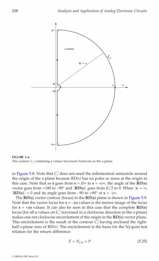
208 Analysis and Application of Analog Electronic Circuits
1¢ does not need the infinitesimal semicircle aroundthe origin of the s-plane because RD(s) has no poles or zeros at the origin inthis case. Note that as s goes from s = j0+ to s = +j, the angle of the RD(s)vector goes from +180 to -90∞ and RD(s) goes from K/2 to 0. When s = ,RD(s) = 0 and its angle goes from -90 to +90∞ at s = -j.
Note that the vector locus for s = -jw values is the mirror image of the locusfor s = +jw values. It can also be seen in this case that the complete RD(s)locus (for all s values on C1¢ traversed in a clockwise direction in the s-plane)makes one net clockwise encirclement of the origin in the RD(s) vector plane.This encirclement is the result of the contour C1¢ having enclosed the right-half s-plane zero of RD(s). The encirclement is the basis for the Nyquist testrelation for the return difference:
Z = NCW + P (5.25)
FIGURE 5.6The contour C1 containing s values traversed clockwise in the s-plane.
jε
−jεε ∞
−j∞
R = ∞
j∞
s-plane
σ
C1
© 2004 by CRC Press LLC
in Figure 5.8. Note that C
The RD(s) vector contour (locus) in the RD(s) plane is shown in Figure 5.9.
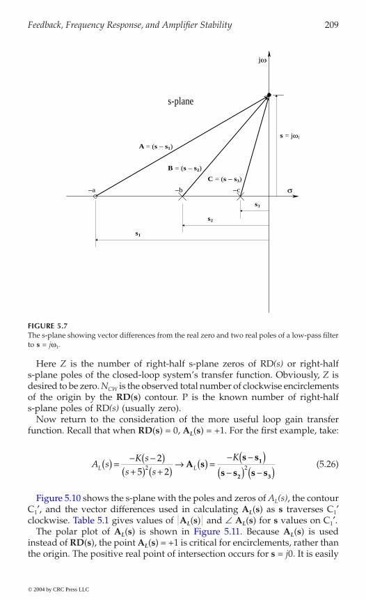
Feedback, Frequency Response, and Amplifier Stability 209
Here Z is the number of right-half s-plane zeros of RD(s) or right-halfs-plane poles of the closed-loop system’s transfer function. Obviously, Z isdesired to be zero. NCW is the observed total number of clockwise encirclementsof the origin by the RD(s) contour. P is the known number of right-halfs-plane poles of RD(s) (usually zero).
Now return to the consideration of the more useful loop gain transferfunction. Recall that when RD(s) = 0, AL(s) = +1. For the first example, take:
(5.26)
L
C1¢, and the vector differences used in calculating AL(s) as s traverses C1¢L L 1
L L
instead of RD(s), the point AL(s) = +1 is critical for encirclements, rather thanthe origin. The positive real point of intersection occurs for s = j0. It is easily
FIGURE 5.7The s-plane showing vector differences from the real zero and two real poles of a low-pass filterto s = jw1.
jω
σ
s3
s2
−a −b −c
s = jω1
A = (s − s1)
B = (s − s2)
C = (s − s3)
s-plane
s1
A sK s
s s
KL L( ) = - -( )
+( ) +( )Æ ( ) =
- -( )-( ) -( )
25 22 2A s
s s
s s s s1
2 3
© 2004 by CRC Press LLC
clockwise. Table 5.1 gives values of A (s) and A (s) for s values on C ¢.
Figure 5.10 shows the s-plane with the poles and zeros of A (s), the contour
The polar plot of A (s) is shown in Figure 5.11. Because A (s) is used
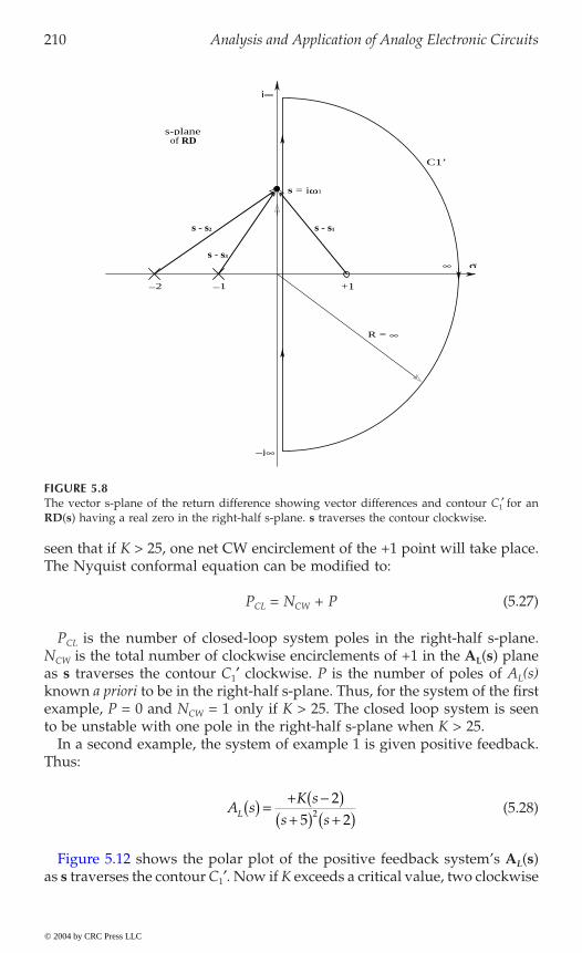
210 Analysis and Application of Analog Electronic Circuits
seen that if K > 25, one net CW encirclement of the +1 point will take place.The Nyquist conformal equation can be modified to:
PCL = NCW + P (5.27)
PCL is the number of closed-loop system poles in the right-half s-plane.NCW is the total number of clockwise encirclements of +1 in the AL(s) planeas s traverses the contour C1¢ clockwise. P is the number of poles of AL(s)known a priori to be in the right-half s-plane. Thus, for the system of the firstexample, P = 0 and NCW = 1 only if K > 25. The closed loop system is seento be unstable with one pole in the right-half s-plane when K > 25.
In a second example, the system of example 1 is given positive feedback.Thus:
(5.28)
L
as s traverses the contour C1¢. Now if K exceeds a critical value, two clockwise
FIGURE 5.8The vector s-plane of the return difference showing vector differences and contour C1¢ for anRD(s) having a real zero in the right-half s-plane. s traverses the contour clockwise.
s = jω1
∞
+1−1−2
R = ∞
s - s1s - s2
s - s3
σ
j∞
−j∞
of RDs-plane
C1’
A sK s
s sL ( ) = + -( )+( ) +( )
25 22
© 2004 by CRC Press LLC
Figure 5.12 shows the polar plot of the positive feedback system’s A (s)

Feedback, Frequency Response, and Amplifier Stability 211
encirclements of +1 will occur, so two closed-loop system poles will be inthe right-half s-plane. Under these conditions, the instability will be a sinu-soidal oscillation with an exponentially growing amplitude. To find thecritical value of K for instability, it is convenient first to find the s = jwo valueat which the system will oscillate by examining the phase of AL(jwo) whereAL crosses the positive real axis:
- 2 tan-1(wo/5) - tan-1(wo/2) + [180∞ - tan-1(wo/2)] = 0° (5.29A)
Ø
- 2 tan-1(wo/5) - 2 tan-1(wo/2) = -180∞ (5.29B)
Ø
tan-1(wo/5) + tan-1(wo/2) = 90∞ (5.29C)
Trial and error solution of Equation 5.29C yields wo = 3.162 r/s. Substitutingthis wo value into AL(jwo) = +1 and solving for K yields K = 35.00. Therefore,if K > 35, the positive feedback system is unstable, with two net CW encir-clements of +1 and thus a complex-conjugate pole pair in the right-half
FIGURE 5.9The vector contour in the polar (complex) plane of the RD(s) of Equation 5.24 as s traversesC1¢ clockwise.
K/2
−180o
−270o
−360o
−450o
ω > 0
ω < 0
ωo
Polar plane
RD
ω = 0ω = ∞
© 2004 by CRC Press LLC
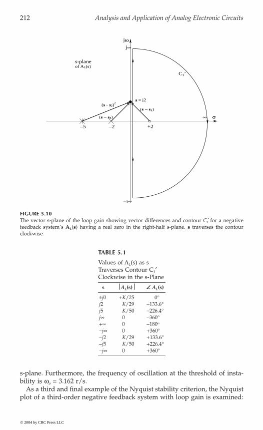
212 Analysis and Application of Analog Electronic Circuits
s-plane. Furthermore, the frequency of oscillation at the threshold of insta-bility is wo = 3.162 r/s.
As a third and final example of the Nyquist stability criterion, the Nyquistplot of a third-order negative feedback system with loop gain is examined:
FIGURE 5.10The vector s-plane of the loop gain showing vector differences and contour C1¢ for a negativefeedback system’s AL(s) having a real zero in the right-half s-plane. s traverses the contourclockwise.
TABLE 5.1
Values of AL(s) as s Traverses Contour C1¢ Clockwise in the s-Plane
s ΩΩΩΩAL(s)ΩΩΩΩ AL(s)
±j0 +K/25 0∞j2 K/29 -133.6∞j5 K/50 -226.4∞j 0 -360∞+ 0 -180o
-j 0 +360∞-j2 K/29 +133.6∞-j5 K/50 +226.4∞-j 0 +360∞
σ∞
−5 −2 +2
s-plane
jω
(s − s1)
(s − s3)
s = j2(s - s2)
2
C1’
of AL(s)
−j∞
j∞
© 2004 by CRC Press LLC

Feedback, Frequency Response, and Amplifier Stability 213
(5.30)
This system has a pole at the origin, so in examining AL(s), s must followthe contour C1 with the infinitesimal semicircle of radius e avoiding theorigin. Start at s = je and go to s = j. At s = je, AL(s) Æ and AL =–270∞. Because s Æ j, AL(s) Æ 0 and AL Æ -450∞. Now when s traversesthe radius semicircle on C1, AL(s) = 0 and the phase goes through 0∞ andthen to +90∞, all with AL(s) = 0. Now as s goes from -j to -je, AL(s) grows larger and its phase goes from +90 to -90∞ (or +270∞). As s traversesthe small semicircle part of C1, AL(s) Æ and the phase goes from -90°to -180∞ at s = e, and then to -270∞ at s = je.
L
large enough, there are two CW encirclements of +1 by the AL(s) locus,signifying two closed-loop system poles in the right-hand s-plane and thusoscillatory instability. Because AL(jwo) is real, it is possible to set the imaginaryterms in the denominator of AL(jwo) = 0 and solve for wo. Thus:
jwo (jwo + 5)(jwo + 2) = - jwo3 - 7wo
2 + 10 jwo = real (5.31)
and (-jwo3 + 10 jwo) = 0 or wo = 3.162 r/s and Kb > 7wo
2 = 70 for instability.
FIGURE 5.11The Nyquist vector contour of the SISO negative feedback system’s AL(s) as s traverses C1¢.Note that this type of contour is always symmetrical around the real axis, and is closed becauseC1¢ is also closed. See text for discussion of stability.
−270o
−360o
j2
j5
−j2
−j5
−90o
−180o
Polar plane
∠AL
of AL
ω = +0K/25
A sK
s s sL ( ) = -+( ) +( )
b5 2
© 2004 by CRC Press LLC
The complete contour, A (s), is shown in Figure 5.13. Note that if Kb is

214 Analysis and Application of Analog Electronic Circuits
5.4 Use of Root Locus in Feedback Amplifier Design
Given the knowledge of the positions of the poles and zeros of the loop gainof a linear SISO single-loop feedback system, the root-locus technique allowsone to predict precisely where the closed-loop poles of the system will be asa function of system gain. Thus, root locus (RL) can be used to predict theconditions for instability, as well as to design for a desired closed-looptransient response. Many texts on linear control systems treat the generationand interpretation of root-locus plots in detail (Kuo, 1982; Ogata, 1990). Rootlocus has also been used in the design of electronic feedback amplifiers,including sinusoidal oscillators (Northrop, 1990).
It is often tedious to construct root-locus diagrams by hand on paper,except in certain simple cases described later. Detailed quantitative RL plotscan be generated using the Matlab subroutine, “RLOCUS.” Several of theexamples in this section are from Matlab plots.
simple one-loop linear SISO feedback system. The closed-loop gain is:
(5.32)
FIGURE 5.12The Nyquist vector contour of the SISO positive feedback system’s AL(s) as s traverses C1¢. This
+180o
+90o
0o
ω = 2
Polar plane
ω = 5
+1
ω = 0+
-K/25
YX
sC s G s
A s
C s G s
C s G s H sp
L
p
p
( ) =( ) ( )- ( ) =
( ) ( )+ ( ) ( ) ( )1 1
© 2004 by CRC Press LLC
is the same system as in Figure 5.11, except it has PFB.
The concept behind the root-locus diagram is simple: Figure 5.14 shows a

Feedback, Frequency Response, and Amplifier Stability 215
C(s) is the controller transfer function acting on E(s); Gp(s) is the planttransfer function (input U(s), output Y(s)), and H(s) is the feedback pathtransfer function. The system loop gain is:
AL(s) = -C(s)Gp(s)H(s) (5.33)
(The minus sign indicates that the system uses negative feedback.)
FIGURE 5.13The Nyquist vector contour plot of the NFB AL(s) of Equation 5.30. This AL(s) has a pole at theorigin.
FIGURE 5.14A three-block SISO system with negative feedback.
∞ @ s = jε
∞ @ s = ε +1
ω = 3.162 r/s
−270o, +90o
−360o, 0o
±180o
∞ @ s = −jε
−90o, +270o
AL
H(s)
C(s) Gp(s)
−
YUEX
© 2004 by CRC Press LLC

216 Analysis and Application of Analog Electronic Circuits
The RL technique allows one to plot complex s values that make the returndifference Æ 0 in the s-plane, thus making the closed-loop transfer function,F(s) Æ . The s values that make F(s) Æ are, by definition, the polesof F(s). These poles move in the s-plane as a function of a gain parameterin a predictable, continuous manner as the gain is changed. Because findings values that set AL(s) = 10∞ is the same as setting F(s) = , the root-locusplotting rules are based on finding s values that cause the angle of -AL(s) =-180∞ and -AL(s) = 1. The root-locus plotting rules are based on satisfyingthe angle or the magnitude condition on -AL(s). The vector format of -AL(s)is used to derive the plotting rules.
For example, first assume a feedback system with the loop gain AL(s) givenbelow. Note the three equivalent ways of writing AL(s):
(5.34A)
(5.34B)
(5.34C)
where s1 = -1/t1, s2 = -1/t2, and s3 = -1/t3.For the magnitude criterion, s must satisfy:
(5.35A)
and, for the angle criterion, s must satisfy:
q1 - (q2 + q3) = -180∞ (5.35B)
Nine basic root-locus plotting rules are derived from the preceding angleand magnitude conditions and used for pencil-and-paper construction of RLdiagrams:
1. Number of branches: there is one branch for each pole of AL(s).2. Starting points: locus branches start at the poles of AL(s) for Kb = 0.3. End points: The branches end at the finite zeros of AL(s) for Kb Æ .
Some zeros of AL(s) can be at s = .4. Behavior of the loci on the real axis (from the angle criterion): For a
negative feedback system, on real-axis locus branches exist to the
A sK s
s sL ( ) =- +( )
+( ) +( ) ( )b tt t
1
2 3
11 1
time-constant form
A sK s
s sL ( ) = - +( )+( ) +( ) ( )bt
t tt
t t1
2 3
1
2 3
11 1
Laplace form
- ( ) = - -( )-( ) -( ) ( )A s
s s
s s s sL1
2 3
Kbtt t
1
2 3
vector form
s s
s s s s1
2 3
-- -
=t t
bt2 3
1K
© 2004 by CRC Press LLC
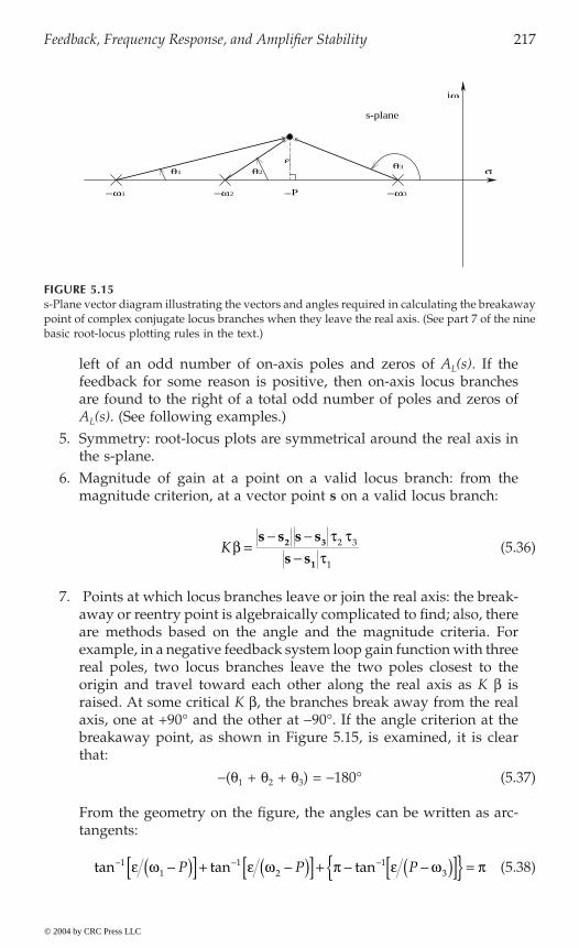
Feedback, Frequency Response, and Amplifier Stability 217
left of an odd number of on-axis poles and zeros of AL(s). If thefeedback for some reason is positive, then on-axis locus branchesare found to the right of a total odd number of poles and zeros ofAL(s). (See following examples.)
5. Symmetry: root-locus plots are symmetrical around the real axis inthe s-plane.
6. Magnitude of gain at a point on a valid locus branch: from themagnitude criterion, at a vector point s on a valid locus branch:
(5.36)
7. Points at which locus branches leave or join the real axis: the break-away or reentry point is algebraically complicated to find; also, thereare methods based on the angle and the magnitude criteria. Forexample, in a negative feedback system loop gain function with threereal poles, two locus branches leave the two poles closest to theorigin and travel toward each other along the real axis as K b israised. At some critical K b, the branches break away from the realaxis, one at +90∞ and the other at -90∞. If the angle criterion at thebreakaway point, as shown in Figure 5.15, is examined, it is clearthat:
-(q1 + q2 + q3) = -180∞ (5.37)
From the geometry on the figure, the angles can be written as arc-tangents:
(5.38)
FIGURE 5.15s-Plane vector diagram illustrating the vectors and angles required in calculating the breakawaypoint of complex conjugate locus branches when they leave the real axis. (See part 7 of the ninebasic root-locus plotting rules in the text.)
θ1 θ2
ε θ3
−P−ω1 −ω2 −ω3
σ
jω
s-plane
K bt t
t=
- --
s s s s
s s2 3
1
2 3
1
tan tan tan- - --( )[ ] + -( )[ ] + - -( )[ ] =11
12
13e w e w p e w pP P P
© 2004 by CRC Press LLC
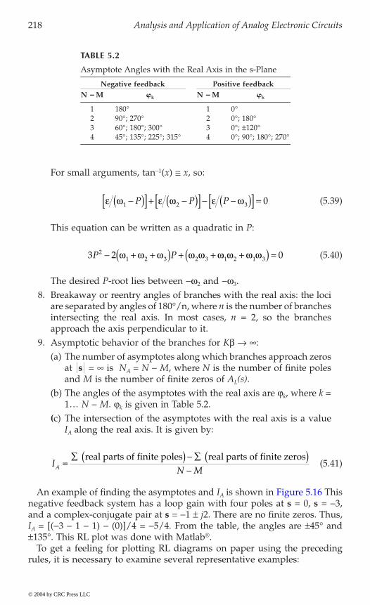
218 Analysis and Application of Analog Electronic Circuits
For small arguments, tan-1(x) @ x, so:
(5.39)
This equation can be written as a quadratic in P:
(5.40)
The desired P-root lies between -w2 and -w3.8. Breakaway or reentry angles of branches with the real axis: the loci
are separated by angles of 180∞/n, where n is the number of branchesintersecting the real axis. In most cases, n = 2, so the branchesapproach the axis perpendicular to it.
9. Asymptotic behavior of the branches for Kb Æ :(a) The number of asymptotes along which branches approach zeros
at s = is NA = N - M, where N is the number of finite polesand M is the number of finite zeros of AL(s).
(b) The angles of the asymptotes with the real axis are jk, where k =1… N - M. jk is given in Table 5.2.
(c) The intersection of the asymptotes with the real axis is a valueIA along the real axis. It is given by:
(5.41)
A
negative feedback system has a loop gain with four poles at s = 0, s = -3,and a complex-conjugate pair at s = -1 ± j2. There are no finite zeros. Thus,IA = [(-3 - 1 - 1) - (0)]/4 = -5/4. From the table, the angles are ±45∞ and±135∞. This RL plot was done with Matlab®.
To get a feeling for plotting RL diagrams on paper using the precedingrules, it is necessary to examine several representative examples:
TABLE 5.2
Asymptote Angles with the Real Axis in the s-Plane
Negative feedback Positive feedbackN ---- M k N ---- M k
1 180∞ 1 0∞2 90∞; 270∞ 2 0∞; 180∞3 60∞; 180∞; 300∞ 3 0∞; ±120∞4 45∞; 135∞; 225∞; 315∞ 4 0∞; 90∞; 180∞; 270∞
e w e w e w1 2 3 0-( )[ ] + -( )[ ] - -( )[ ] =P P P
3 2 021 2 3 2 3 1 2 1 3P P- + +( ) + + +( ) =w w w w w w w w w
IN MA =
 ( ) -  ( )-
real parts of finite poles real parts of finite zeros
© 2004 by CRC Press LLC
An example of finding the asymptotes and I is shown in Figure 5.16 This
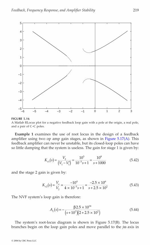
Feedback, Frequency Response, and Amplifier Stability 219
Example 1 examines the use of root locus in the design of a feedback
feedback amplifier can never be unstable, but its closed-loop poles can haveso little damping that the system is useless. The gain for stage 1 is given by:
(5.42)
and the stage 2 gain is given by:
(5.43)
The NVF system’s loop gain is therefore:
(5.44)
The system’s root-locus diagram is shown in Figure 5.17(B). The locusbranches begin on the loop gain poles and move parallel to the jw axis in
FIGURE 5.16A Matlab RLocus plot for a negative feedback loop gain with a pole at the origin, a real pole,and a pair of C–C poles.
K sV
V V s sv12
1 1
5
3
81010 1
101000
( ) =- ¢( ) =
+=
+-
K sVV s sv
o2
2
4
3
6
210
4 10 12 5 102 5 10
( ) = = -¥ +
= - ¥+ ¥-
..
A ssL ( ) = - ¥
+( ) + ¥( )b 2 5 10
10 2 2 5 10
14
3 2
..
© 2004 by CRC Press LLC
amplifier using two op amp gain stages, as shown in Figure 5.17(A). This
5
4
3
2
1
0
–1
–2
–3
–4
–5–6 –5 –4 –3 –2 –1 0 1 2 3

220 Analysis and Application of Analog Electronic Circuits
the s-plane to ±j as b increases. The locus branches meet on the negativereal axis at s = IA, where they become complex-conjugate:
(5.45)
FIGURE 5.17(A) Two op amps connected as a noninverting amplifier with overall NVFB. (B) Root-locusdiagram for the amplifier. Note that unless a sharply tuned closed-loop frequency response isdesired, the feedback gain, b, must be very small to realize a closed-loop system with a dampingfactor of 0.7071.
RF
R1
v2
Vsv2’
v1
Vo
+ v1’Kv1(s) Kv2(s)
B
jω
σ
−2.5 × 10²
ωnBA
−103 r/s −6.25 × 10²
IA
β = R1/(R1 + RF) A
IN MA =
 ( ) -  ( )-
= - - ¥ = - ¥
real parts of finite poles real parts of finite zeros
10 2 5 102
6 25 103 2
2..
© 2004 by CRC Press LLC
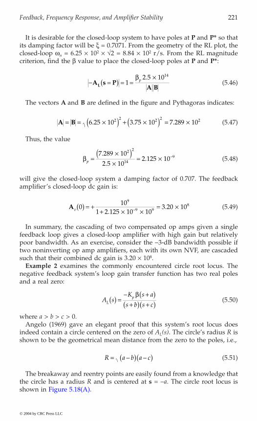
Feedback, Frequency Response, and Amplifier Stability 221
It is desirable for the closed-loop system to have poles at P and P* so thatits damping factor will be x = 0.7071. From the geometry of the RL plot, theclosed-loop wn = 6.25 ¥ 102 ¥ ÷2 = 8.84 ¥ 102 r/s. From the RL magnitudecriterion, find the b value to place the closed-loop poles at P and P*:
(5.46)
The vectors A and B are defined in the figure and Pythagoras indicates:
(5.47)
Thus, the value
(5.48)
will give the closed-loop system a damping factor of 0.707. The feedbackamplifier’s closed-loop dc gain is:
(5.49)
In summary, the cascading of two compensated op amps given a singlefeedback loop gives a closed-loop amplifier with high gain but relativelypoor bandwidth. As an exercise, consider the -3-dB bandwidth possible iftwo noninverting op amp amplifiers, each with its own NVF, are cascadedsuch that their combined dc gain is 3.20 ¥ 108.
Example 2 examines the commonly encountered circle root locus. Thenegative feedback system’s loop gain transfer function has two real polesand a real zero:
(5.50)
where a > b > c > 0.Angelo (1969) gave an elegant proof that this system’s root locus does
indeed contain a circle centered on the zero of AL(s). The circle’s radius R isshown to be the geometrical mean distance from the zero to the poles, i.e.,
(5.51)
The breakaway and reentry points are easily found from a knowledge thatthe circle has a radius R and is centered at s = -a. The circle root locus is
- =( ) = =¥
A s PA BL 1
2 5 1014bp .
A B= = ¥( ) + ¥( ) = ¥6 25 10 3 75 10 7 289 102 2 2 2 2. . .
bp =¥( )
¥= ¥ -7 289 10
2 5 102 125 10
2 2
149.
..
Av 010
1 2 125 10 103 20 10
9
9 98( ) = +
+ ¥ ¥= ¥-.
.
A sK s a
s b s cLp( ) =
- +( )+( ) +( )
b
R a b a c= -( ) -( )
© 2004 by CRC Press LLC
shown in Figure 5.18(A).
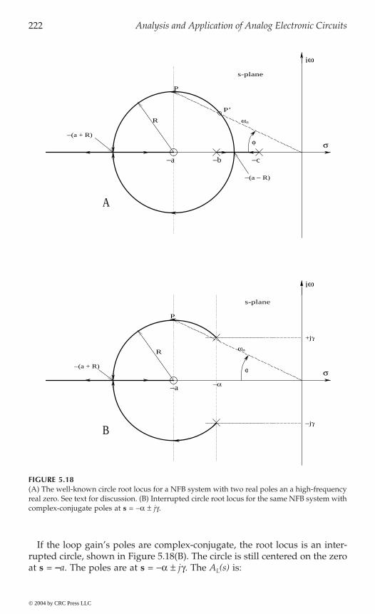
222 Analysis and Application of Analog Electronic Circuits
If the loop gain’s poles are complex-conjugate, the root locus is an inter-rupted circle, shown in Figure 5.18(B). The circle is still centered on the zeroat s = ----a. The poles are at s = -a ± jg. The AL(s) is:
FIGURE 5.18(A) The well-known circle root locus for a NFB system with two real poles an a high-frequencyreal zero. See text for discussion. (B) Interrupted circle root locus for the same NFB system withcomplex-conjugate poles at s = -a ± jg.
−α
+jγ
−jγ
−a
jω
s-plane
σ
σ
jω
−b −c−a
R
−(a + R)
−(a + R)
−(a − R)
P
P’
ωn
φ
φ
R ωn
s-plane
P
A
B
© 2004 by CRC Press LLC

Feedback, Frequency Response, and Amplifier Stability 223
(5.52)
The circle’s radius is now found from the Pythagorean theorem:
(5.53)
Note that as the gain, Kp b, is increased, the closed-loop system polesbecome more and more damped, until they become real, one approachingthe zero at s = –a and the other going to -.
The damping of a complex-conjugate (CC) pole pair in the s-plane can bedetermined quantitatively by drawing a line from the origin to the upper-half plane pole. The damping factor, z, associated with the CC poles can beshown to be the cosine of the angle that the line from the origin to the CCpole makes with the negative real axis, i.e., x = cos(f). If the poles lie closeto the jw axis, f Æ 90∞ and x Æ 0. The length of the line from the origin toone of the CC poles is the undamped natural frequency, wn, of that CC polepair. Recall that the CC pole pair is the result of factoring the quadratic term,[s2 + s(2xwn) + wn
2]. By way of example, the damping of the open-loop CC-1(g/a)] = a/wn.
Many other interesting examples of root-locus plots are to be found in thecontrol systems texts by Kuo (1982) and Ogata (1970) and in the electroniccircuits text by Gray and Meyer (1984). Circle root-locus plots are easy toconstruct graphically by hand. More complex root-locus plots should bedone by computer. In closing, it should be stressed that root-locus plots showthe closed-loop systems poles. Closed-loop zeros can be found algebraically;they are generally fixed (not functions of gain) and do affect system transientresponse. Merely locating the closed-loop poles in an apparently good posi-tion does not necessarily guarantee a step response without an objectionableovershoot.
for linear SISO feedback systems. Locus branches for loop gains with NFB(left column) and for PFB (right column) are shown. The unstable systemsoscillate when complex-conjugate closed-loop pole pairs move into the right-half s-plane; they saturate when one closed-loop pole moves into the right-halfs-plane.
5.5 Use of Root-Locus in the Design of “Linear” Oscillators
5.5.1 Introduction
“Linear” oscillators are used to generate sinusoidal signals for many appli-cations; probably the most important is testing the steady-state sinusoidal
A sK s a
s sLp( ) =
- +( )+ ( ) + +( )
ba a g2 2 22
R a= -( ) +a g2 2
© 2004 by CRC Press LLC
pole pair in Figure 5.18(B) is x = cos[tan
Figure 5.19(A) through Figure 5.19(L) illustrate typical root-locus diagrams

224 Analysis and Application of Analog Electronic Circuits
frequency response of amplifiers. They are also used in measurements as thesignal source for ac bridges used to measure the values of circuit componentsR, L, and C, as well as circuits Z(jw) and Y(jw). Still another oscillator appli-cation is a signal source in acoustic measurements. In biomedicine, oscillatorsare used to power ac current sources in impedance pneumography andplethysmography (Northrop, 2002).
Linear oscillators are called “linear” because the criteria for oscillation arebased on linear circuit theory and root locus, which is applied to linearsystems. In reality, linear oscillators are designed to have a closed-loop,complex-conjugate pole pair in the right-half s-plane so that oscillations,
FIGURE 5.19(A) through (L): Representative root-locus plots for six loop gain configurations for NFB andPFB conditions. PFB root-locus plots are on the right.
A B
DC
E F
G H
© 2004 by CRC Press LLC
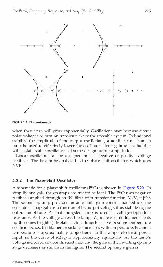
Feedback, Frequency Response, and Amplifier Stability 225
when they start, will grow exponentially. Oscillations start because circuitnoise voltages or turn-on transients excite the unstable system. To limit andstabilize the amplitude of the output oscillations, a nonlinear mechanismmust be used to effectively lower the oscillator’s loop gain to a value thatwill sustain stable oscillations at some design output amplitude.
Linear oscillators can be designed to use negative or positive voltagefeedback. The first to be analyzed is the phase-shift oscillator, which usesNVF.
5.5.2 The Phase-Shift Oscillator
simplify analysis, the op amps are treated as ideal. The PSO uses negativefeedback applied through an RC filter with transfer function, Vi/Vo = b(s).The second op amp provides an automatic gain control that reduces theoscillator’s loop gain as a function of its output voltage, thus stabilizing theoutput amplitude. A small tungsten lamp is used as voltage-dependentresistance. As the voltage across the lamp, Vb, increases, its filament heatsup (becomes brighter). Metals such as tungsten have positive temperaturecoefficients, i.e., the filament resistance increases with temperature. Filamenttemperature is approximately proportional to the lamp’s electrical powerinput, so the curve of Rb(Vb) is approximately square-law. As the lamp’svoltage increases, so does its resistance, and the gain of the inverting op ampstage decreases as shown in the figure. The second op amp’s gain is:
FIGURE 5.19 (continued)
K L
I J
© 2004 by CRC Press LLC
A schematic for a phase-shift oscillator (PSO) is shown in Figure 5.20. To
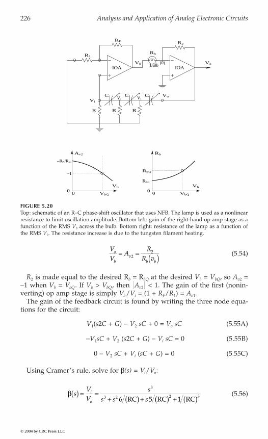
226 Analysis and Application of Analog Electronic Circuits
(5.54)
R2 is made equal to the desired Rb = RbQ at the desired Vb = VbQ, so Av2 =-1 when Vb = VbQ . If Vb > VbQ , then Av2 < 1. The gain of the first (nonin-verting) op amp stage is simply Vb/Vi = (1 + RF/R1) = Av1.
The gain of the feedback circuit is found by writing the three node equa-tions for the circuit:
V1(s2C + G) - V2 sC + 0 = Vo sC (5.55A)
-V1sC + V2 (s2C + G) - Vi sC = 0 (5.55B)
0 - V2 sC + Vi (sC + G) = 0 (5.55C)
Using Cramer’s rule, solve for b(s) = Vi/Vo:
(5.56)
FIGURE 5.20Top: schematic of an R–C phase-shift oscillator that uses NFB. The lamp is used as a nonlinearresistance to limit oscillation amplitude. Bottom left: gain of the right-hand op amp stage as afunction of the RMS Vb across the bulb. Bottom right: resistance of the lamp as a function ofthe RMS Vb. The resistance increase is due to the tungsten filament heating.
RF
Bulb
R1Rb
R2
(0)Vb Vo
R R R
IOA IOA
Rb
RbQ
Rbo
VbQ
VbVb
0 00 0VbQ
Av2
−1
−R2 /Rbo
Vi
VoCCCV1V2
VV
AR
R vo
bv
b b
= = ( )22
b sVV
ss s s
i
o
( ) = =+ ( ) + ( ) + ( )
3
3 2 2 36 5 1RC RC RC
© 2004 by CRC Press LLC
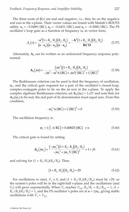
Feedback, Frequency Response, and Amplifier Stability 227
The three roots of b(s) are real and negative, i.e., they lie on the negativereal axis in the s-plane. Their vector values are found with Matlab’s ROOTSutility: s1 = -5.0489/(RC), s2 = -0.6431/(RC) and s3 = -0.3080/(RC). The PSoscillator’s loop gain as a function of frequency is, in vector form,
(5.57)
Alternately, AL can be written as an unfactored frequency response poly-nomial:
(5.58)
The Barkhausen criterion can be used to find the frequency of oscillation,wo, and the critical gain required for a pair of the oscillator’s closed-loop,complex-conjugate poles to lie on the jw axis in the s-plane. To apply thecomplex algebraic Barkhausen criterion, set AL(jwo) = 10∞ and note that, forAL(jwo) to be real, the real part of its denominator must equal zero. From thiscondition,
(5.59)
The oscillation frequency is:
(5.60)
The critical gain is found by setting
(5.61)
and solving for (1 + RF/R1)(R2/Rb). Thus:
(5.62)
For oscillations to start, Vb @ 0, and (1 + RF/R1)(R2/Rbo) must be >29, sothe system’s poles will be in the right-half s-plane and the oscillations (andVb) will grow exponentially. When Vb reaches VbQ, R2/Rb = R2/RbQ = 1, (1 +RF /R1)(R2/Rb) = 1, and the PS oscillator’s poles are at s = ±jwo, giving stableoscillations with Vo = VbQ.
A sR R R R R R R R
LF b F b( ) =
- +( )( )-( ) -( ) -( ) =
- +( )( )s
s s s s s s
A
BCD
3
1 2 3
31 11 2 1 2
AL jj R R R R
j jF bw
w
w w w( ) =
( ) +( )( )- - ( ) + ( ) + ( )
31 2
3 2 2 3
1
6 5 1RC RC RC
- ( ) + ( ) =wo2 36 1 0RC RC
wo = ( ) = ( )1 6 0 40825 RC RC r s.
AL jj R R R R
j jjo
o F b
o o
ww
w w( ) =
-( ) +( )( )- + ( )
= +3
1 23 2
1
51 0
RC
1 291 2+( ) ( ) =R R R RF b
© 2004 by CRC Press LLC
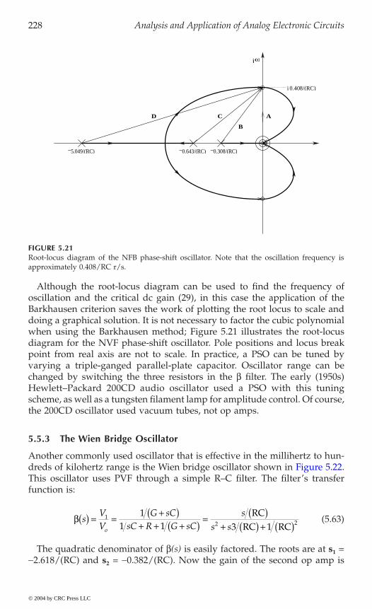
228 Analysis and Application of Analog Electronic Circuits
Although the root-locus diagram can be used to find the frequency ofoscillation and the critical dc gain (29), in this case the application of theBarkhausen criterion saves the work of plotting the root locus to scale anddoing a graphical solution. It is not necessary to factor the cubic polynomialwhen using the Barkhausen method; Figure 5.21 illustrates the root-locusdiagram for the NVF phase-shift oscillator. Pole positions and locus breakpoint from real axis are not to scale. In practice, a PSO can be tuned byvarying a triple-ganged parallel-plate capacitor. Oscillator range can bechanged by switching the three resistors in the b filter. The early (1950s)Hewlett–Packard 200CD audio oscillator used a PSO with this tuningscheme, as well as a tungsten filament lamp for amplitude control. Of course,the 200CD oscillator used vacuum tubes, not op amps.
5.5.3 The Wien Bridge Oscillator
Another commonly used oscillator that is effective in the millihertz to hun-
This oscillator uses PVF through a simple R–C filter. The filter’s transferfunction is:
(5.63)
The quadratic denominator of b(s) is easily factored. The roots are at s1 =-2.618/(RC) and s2 = -0.382/(RC). Now the gain of the second op amp is
FIGURE 5.21Root-locus diagram of the NFB phase-shift oscillator. Note that the oscillation frequency isapproximately 0.408/RC r/s.
−5.049/(RC) −0.643/(RC) −0.308/(RC)
A
B
CD
j 0.408/(RC)
jω
b sVV
G sCsC R G sC
ss so
( ) = = +( )+ + +( ) = ( )
+ ( ) + ( )1
2 21
1 1 3 1RC
RC RC
© 2004 by CRC Press LLC
dreds of kilohertz range is the Wien bridge oscillator shown in Figure 5.22.
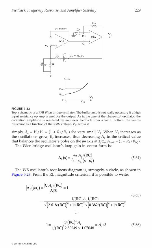
Feedback, Frequency Response, and Amplifier Stability 229
simply Av = Vo/V1 = (1 + RF/Rbo ) for very small V1. When V1 increases asthe oscillations grow, Rb increases, thus decreasing Av to the critical valuethat balances the oscillator’s poles on the jw axis at ±jwo; Avcrit = (1 + RF/RbQ).
The Wien bridge oscillator’s loop gain in vector form is:
(5.64)
The WB oscillator’s root-locus diagram is, strangely, a circle, as shown in
(5.65)
Ø
(5.66)
FIGURE 5.22Top: schematic of a PFB Wien bridge oscillator. The buffer amp is not really necessary if a highinput resistance op amp is used for the output. As in the case of the phase-shift oscillator, theoscillation amplitude is regulated by nonlinear feedback from a lamp. Bottom: the lamp’sresistance as a function of the RMS voltage, V1, across it.
RC
IOA
IOA
Rb
RF
V1
(×1 Buffer)
Vo(V1)
V1
CR Vo = AvV1
Rb
RbQ
Rbo
00
V1
V1Q
A ss
s s s sL1 2
( ) =+ ( )
-( ) -( )Av RC
AC
A BL jA
A
ov
v
w( ) = ( ) =
= ( ) ( )÷ ( )[ ] + ( ) ÷ ( )[ ] + ( )
RC
RC RC
RC RC RC RC
1
1 1
2 618 1 0 382 12 2 2 2. .
11
1 2 80249 1 070483
2
2= ( )( ) ¥
=RC
RCA
Avv. .
© 2004 by CRC Press LLC
Figure 5.23. From the RL magnitude criterion, it is possible to write:
230 Analysis and Application of Analog Electronic Circuits
Thus, when Avcrit = 3, the WB oscillator’s poles are on the jw axis at s =±j/(RC), the condition that sustains steady-state output oscillations of ampli-tude Vo = 3V1Q.
The Wien bridge and the phase-shift oscillators described have low totalharmonic distortion (THD) in their outputs. The low distortion is the resultof using the tungsten lamp in the automatic gain control nonlinearity. Otheroscillators that use diode or zener diode clipping to regulate the oscillator’sloop gain have outputs with greater THD.
5.6 Chapter Summary
This chapter began with a review of the frequency response as a descriptorfor linear amplifier performance. The basics of Bode plotting an amplifier’sfrequency response were examined, including the use of asymptotes to expe-dite pencil-and-paper Bode plots, given an amplifier’s transfer function orfrequency response function. How to obtain the frequency response phasefunction from the frequency response function was also covered.
The concept of amplifier stability was set forth and stability was consideredfrom the viewpoint of the location of a system’s poles in the s-plane. Variousstability tests were mentioned, and the root-locus (RL) technique wasstressed as a useful method for characterizing a linear feedback system’sclosed-loop poles as a function of gain. Root-locus plotting rules were givenwith examples of RL plots. Application of the RL method was given in the
FIGURE 5.23The Wien bridge oscillator’s root-locus diagram. Oscillation frequency is near 1/RC r/s.
−2.618/(RC) −0.382/(RC)
jω
σ
−1/(RC)
jωo = j/(RC)
A B C
1/(RC)
© 2004 by CRC Press LLC

Feedback, Frequency Response, and Amplifier Stability 231
design of feedback amplifiers with useful pole locations. The design of thephase-shift oscillator and the Wien bridge oscillator were shown to be madeeasier with the RL method. The venerable Barkhausen technique was intro-duced as an alternate to RL analysis.
Home Problems
5.1 A power op amp is used to drive a CRT deflection yoke coil as shown inFigure P5.1. Assume that the op amp is ideal except for finite differential gain,Vo = Kv (Vi - Vi¢). Negative current feedback is used to increase the frequencyresponse of the coil current, IL, thus the coil’s B field. Assume the current fromthe VF node into RF is negligible, L = 0.01 Hy; RL = 0.5 W; R1 = 104 W; RF =104 W; Kv = 104; RM = 1 W; and RF, R1 RM.
a. Derive an algebraic expression for the amplifier’s transfer admit-tance, YL(jw) = IL/V1, in time V1 constant form. Show what hap-pens to YL(jw) as Kv. gets very large.
b. Evaluate YL(jw) numerically. Give the time constant of the coilwith and without feedback.
5.2 Negative voltage feedback is used to extend the bandwidth of a differential
the transfer function:
FIGURE P5.1
RL
ILL
RM
1Ω
POA
RF
R1
V1
VoVi’
VF
↑0
VV V
s soi i=
- ¢( )+( ) ¥ +( )- -
10
10 1 2 10 1
3
3 4
© 2004 by CRC Press LLC
amplifier (not an op amp), as shown in Figure P5.2. The DA gain is given by
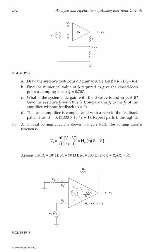
232 Analysis and Application of Analog Electronic Circuits
a. Draw the system’s root-locus diagram to scale. Let b ∫ R1/(R1 + RF).b. Find the numerical value of b required to give the closed-loop
poles a damping factor x = 0.707.c. What is the system’s dc gain with the b value found in part B?
Give the system’s fT with this b. Compare this fT to the fT of theamplifier without feedback (b = 0).
d. The same amplifier is compensated with a zero in the feedbackpath. Thus, b = bo (3.333 ¥ 10-5 s + 1). Repeat parts b through d.
5.3 A nonideal op amp circuit is shown in Figure P5.3. The op amp transferfunction is:
Assume that R1 = 104 W; RF = 90 kW; Ro = 100 W; and b = R1/(R1 + RF).
FIGURE P5.2
FIGURE P5.3
Vo
βVo
RF
R1
Vi
Vi’V1
DA
VV V
ss V Vo
i ioc i i=
- ¢( )+( ) = ( ) - ¢( )-
10
10 1
4
3 H
Vi
V1
RF
Vo
Vi’
βVoR1
Ro+
Hoc(s)(Vi − Vi’)
Io
© 2004 by CRC Press LLC
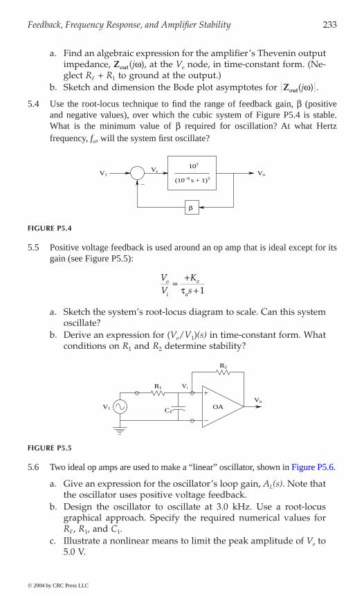
Feedback, Frequency Response, and Amplifier Stability 233
a. Find an algebraic expression for the amplifier’s Thevenin outputimpedance, Zout (jw), at the Vo node, in time-constant form. (Ne-glect RF + R1 to ground at the output.)
b. Sketch and dimension the Bode plot asymptotes for Zout(jw) .
5.4 Use the root-locus technique to find the range of feedback gain, b (positiveand negative values), over which the cubic system of Figure P5.4 is stable.What is the minimum value of b required for oscillation? At what Hertzfrequency, fo, will the system first oscillate?
5.5 Positive voltage feedback is used around an op amp that is ideal except for itsgain (see Figure P5.5):
a. Sketch the system’s root-locus diagram to scale. Can this systemoscillate?
b. Derive an expression for (Vo/V1)(s) in time-constant form. Whatconditions on R1 and R2 determine stability?
5.6
a. Give an expression for the oscillator’s loop gain, AL(s). Note thatthe oscillator uses positive voltage feedback.
b. Design the oscillator to oscillate at 3.0 kHz. Use a root-locusgraphical approach. Specify the required numerical values forRF, R1, and C1.
c. Illustrate a nonlinear means to limit the peak amplitude of Vo to5.0 V.
FIGURE P5.4
FIGURE P5.5
−
β
(10−6 s + 1)3
102
VoVeV1
VV
Ks
o
i
v
a
=+
+t 1
V1
R1
C1
R2
Vo
OA
Vi
© 2004 by CRC Press LLC
Two ideal op amps are used to make a “linear” oscillator, shown in Figure P5.6.
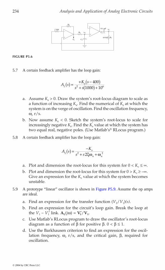
234 Analysis and Application of Analog Electronic Circuits
5.7 A certain feedback amplifier has the loop gain:
a. Assume Ka > 0. Draw the system’s root-locus diagram to scale asa function of increasing Ka. Find the numerical of Ka at which thesystem is on the verge of oscillation. Find the oscillation frequency,wo r/s.
b. Now assume Ka < 0. Sketch the system’s root-locus to scale forincreasingly negative Ka. Find the Ka value at which the system hastwo equal real, negative poles. (Use Matlab’s® RLocus program.)
5.8 A certain feedback amplifier has the loop gain:
a. Plot and dimension the root-locus for this system for 0 < Kv £ .b. Plot and dimension the root-locus for this system for 0 > Kv ≥ –.
Give an expression for the Kv value at which the system becomesunstable.
5.9are ideal.
a. Find an expression for the transfer function (V2/V1)(s).b. Find an expression for the circuit’s loop gain. Break the loop at
the V1 – V1¢ link. AL(jw) = V1¢/V1.c. Use Matlab’s RLocus program to draw the oscillator’s root-locus
diagram as a function of b for positive b. 0 < b £ 1.d. Use the Barkhausen criterion to find an expression for the oscil-
lation frequency, wo r/s, and the critical gain, b, required foroscillation.
FIGURE P5.6
RF
V1
V2
0.1 µF
10 kΩ R2
C2R1
Vo C1
1 kΩ
A sK s
s sLa( ) =
+ -( )+ ( ) +
4001000 102 6
A sK
s sLv
n n
( ) =-
+ +2 22xw w
© 2004 by CRC Press LLC
A prototype “linear” oscillator is shown in Figure P5.9. Assume the op amps

Feedback, Frequency Response, and Amplifier Stability 235
5.10 An otherwise ideal op amp has the gain:
The op amp is connected as a simple inverting gain amplifier, as shown inFigure P5.10.
a. Find the maximum dc gain the amplifier can possess and havea -3-dB frequency of 50 kHz. That is, find the RF required.
b. For the RF of part a, find the inverting amplifier’s fT.
5.11described in NASA Tech Briefs #GSC-13309. The purpose of the circuit is topresent a multiturn magnetic search coil with a negative terminatingimpedance that, when summed with the series impedance of the coil, forms avery low Thevenin impedance. This allows more current, Is, to flow from the
FIGURE P5.9
FIGURE P5.10
C C CR
R
R
R R
R
V1
V2 V3
V4
βV4
IOA IOA IOA
V1’ IOA
Vo
VV
ss
o
i¢( ) = -
+-10
10 1
5
2
Vi’R1
1 kΩ
RF
Vo
V1
OA
© 2004 by CRC Press LLC
Figure P5.11B illustrates a “regenerative magnetic pickup circuit” as

236 Analysis and Application of Analog Electronic Circuits
open-circuit induced voltage, Vs = NF• , where N is the number of turns of thesearch coil and F• is the time rate of change of the magnetic flux linking thecoil’s area. The op amp, less search coil, forms what is called a negative
amp is ideal in this analysis.
a. Refer to Figure P5.11A. Find an expression for the transfer func-tion, Vo/Vs(s). Let Ls = 0.01 Hy; Rs = 100 W; and R3 = 104. Alsoevaluate the transfer function’s break frequency, fb = wb/2p andits dc gain.
b. Refer to Figure P5.11B. Replace the search coil (Ls, Rs) with justthe voltage source, Vs. Find expressions for the input current, Is,and the input impedance looking into the Vi¢ node. (Note that itemulates a negative inductance.)
c. Now consider the search coil in place with open-circuit, inducedEMF, Vs. Derive an expression for Vo/Vs(s) in time-constant form.Comment on the conditions on the circuit parameters (R1, R2, R3,and C) that will make the circuit unstable or the dc gain infinite.
5.12 Negative voltage feedback and positive current feedback are used on a power
differential gain:
Assume that (R1 + R2) (R3 + R4); a ∫ R2/(R1 + R2); b ∫ R1/(R1 + R2); and g ∫R4 /(R3 + R4).
A B
FIGURE P5.11
R1
C
R2
R3 R3
Ls Ls
Rs Rs
Vs Vs
Is Is
IOA I OAVo Vo
Vi Vi
Vi’ V i’
+ +
VK V V
sovo i i=
- ¢( )+t 1
© 2004 by CRC Press LLC
op amp circuit, shown in Figure P5.12. The op amp is ideal except for the
impedance converter circuit (NIC) (Ghaussi, 1971, Chapter 8). Assume the op

Feedback, Frequency Response, and Amplifier Stability 237
a. Assume op amp Rout = 0. Find an expression for Vo/V1 in time-constant form. Comment how the PVFB affects the dc gain, cor-ner frequency, and gain-bandwidth product.
b. Now let Rout > 0. Replace the load resistor, R3, with a test voltagesource, vt, to find an expression for the Thevenin output resis-tance that R3 “sees.”
5.13 It is desired to measure the slew rate of a prototype op amp design physically.The linear small-signal behavior of the op amp is known to be Vo = (Vi -Vi¢)105/(10-3 s + 1). The op amp is connected as a unity-gain follower, asshown in Figure P5.13A.
a. Find Vo/Vs(s) in Laplace form. What is the follower’s time constant?b. A step input of 100 mV is given, i.e., Vs(s) = 0.1/s. Sketch and
dimension vo(t) at the follower output. What is the maximumslope of vo(t)?
c. The follower’s response to a 10-V input step, Vs(s) = 10/s, isshown in Figure P5.13B. Estimate the op amp’s slew rate, h, inV/msec. Sketch and dimension vo(t) to the 10-V step when theslew rate is assumed to be infinite.
FIGURE P5.12
A B
FIGURE P5.13
R4
R3
Vo
R1
R2
γVo
V1
Vi
Vi’POA
vo(t)
100 ns
10 V
00
vo
vs
vi
vi’
OA
t
© 2004 by CRC Press LLC

238 Analysis and Application of Analog Electronic Circuits
5.14 A certain op amp has open-loop poles at f1 = 100 Hz and at f2 = 100 kHz, anda negative real zero at f0 = 110 kHz. Its dc gain is 105. The op amp is connected
amplifier’s root-locus diagram as a function of the closed-loop dc gain, Vo/Vs =
(R1 + RF)/R1. Let Vo/Vs range from 1 to 103.
© 2004 by CRC Press LLC
as a noninverting amplifier (see text Figure 6.1(C)). Plot and dimension the
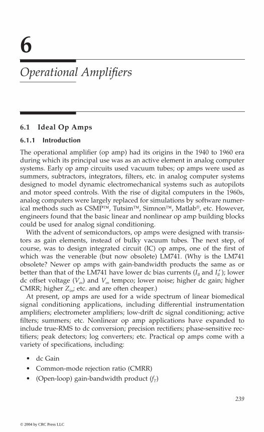
239
6Operational Amplifiers
6.1 Ideal Op Amps
6.1.1 Introduction
The operational amplifier (op amp) had its origins in the 1940 to 1960 eraduring which its principal use was as an active element in analog computersystems. Early op amp circuits used vacuum tubes; op amps were used assummers, subtractors, integrators, filters, etc. in analog computer systemsdesigned to model dynamic electromechanical systems such as autopilotsand motor speed controls. With the rise of digital computers in the 1960s,analog computers were largely replaced for simulations by software numer-ical methods such as CSMP, Tutsim, Simnon, Matlab®, etc. However,engineers found that the basic linear and nonlinear op amp building blockscould be used for analog signal conditioning.
With the advent of semiconductors, op amps were designed with transis-tors as gain elements, instead of bulky vacuum tubes. The next step, ofcourse, was to design integrated circuit (IC) op amps, one of the first ofwhich was the venerable (but now obsolete) LM741. (Why is the LM741obsolete? Newer op amps with gain-bandwidth products the same as orbetter than that of the LM741 have lower dc bias currents (IB and IB¢ ); lowerdc offset voltage (Vos) and Vos tempco; lower noise; higher dc gain; higherCMRR; higher Zin; etc. and are often cheaper.)
At present, op amps are used for a wide spectrum of linear biomedicalsignal conditioning applications, including differential instrumentationamplifiers; electrometer amplifiers; low-drift dc signal conditioning; activefilters; summers; etc. Nonlinear op amp applications have expanded toinclude true-RMS to dc conversion; precision rectifiers; phase-sensitive rec-tifiers; peak detectors; log converters; etc. Practical op amps come with avariety of specifications, including:
• dc Gain• Common-mode rejection ratio (CMRR)• (Open-loop) gain-bandwidth product (fT)
© 2004 by CRC Press LLC
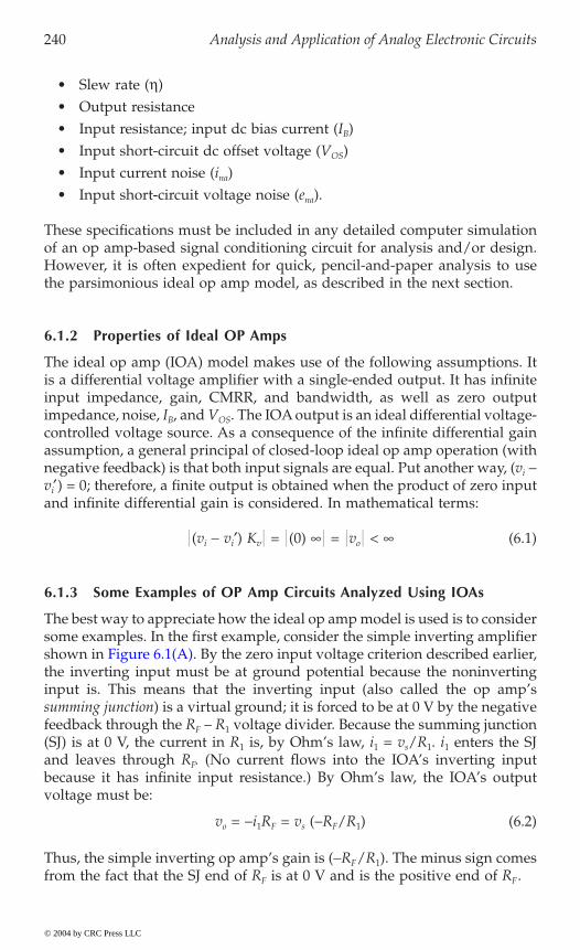
240 Analysis and Application of Analog Electronic Circuits
• Slew rate (h)• Output resistance• Input resistance; input dc bias current (IB)• Input short-circuit dc offset voltage (VOS)• Input current noise (ina)• Input short-circuit voltage noise (ena).
These specifications must be included in any detailed computer simulationof an op amp-based signal conditioning circuit for analysis and/or design.However, it is often expedient for quick, pencil-and-paper analysis to usethe parsimonious ideal op amp model, as described in the next section.
6.1.2 Properties of Ideal OP Amps
The ideal op amp (IOA) model makes use of the following assumptions. Itis a differential voltage amplifier with a single-ended output. It has infiniteinput impedance, gain, CMRR, and bandwidth, as well as zero outputimpedance, noise, IB, and VOS. The IOA output is an ideal differential voltage-controlled voltage source. As a consequence of the infinite differential gainassumption, a general principal of closed-loop ideal op amp operation (withnegative feedback) is that both input signals are equal. Put another way, (vi -vi¢) = 0; therefore, a finite output is obtained when the product of zero inputand infinite differential gain is considered. In mathematical terms:
(vi - vi¢) Kv = (0) = vo < (6.1)
6.1.3 Some Examples of OP Amp Circuits Analyzed Using IOAs
The best way to appreciate how the ideal op amp model is used is to considersome examples. In the first example, consider the simple inverting amplifier
the inverting input must be at ground potential because the noninvertinginput is. This means that the inverting input (also called the op amp’ssumming junction) is a virtual ground; it is forced to be at 0 V by the negativefeedback through the RF – R1 voltage divider. Because the summing junction(SJ) is at 0 V, the current in R1 is, by Ohm’s law, i1 = vs/R1. i1 enters the SJand leaves through RF. (No current flows into the IOA’s inverting inputbecause it has infinite input resistance.) By Ohm’s law, the IOA’s outputvoltage must be:
vo = -i1RF = vs (-RF/R1) (6.2)
Thus, the simple inverting op amp’s gain is (-RF/R1). The minus sign comesfrom the fact that the SJ end of RF is at 0 V and is the positive end of RF.
© 2004 by CRC Press LLC
shown in Figure 6.1(A). By the zero input voltage criterion described earlier,
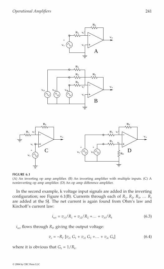
Operational Amplifiers 241
In the second example, k voltage input signals are added in the invertingconfiguration; see Figure 6.1(B). Currents through each of R1, R2, R3, … Rk
are added at the SJ. The net current is again found from Ohm’s law andKirchoff’s current law:
inet = vs1/R1 + vs2/R2 +… + vsk/Rk (6.3)
inet flows through RF, giving the output voltage:
vo = -RF [vs1 G1 + vs2 G2 +… + vsk Gk] (6.4)
where it is obvious that Gk = 1/Rk.
FIGURE 6.1(A) An inverting op amp amplifier. (B) An inverting amplifier with multiple inputs. (C) Anoninverting op amp amplifier. (D) An op amp difference amplifier.
RF
RF
RF RF
RF
R1
R1
R2
A
B
C D
vs2 vsk
.
.
.
vs1
vs’ vs
vs
vi
R1R1 vi’vi’
vi’
vs vi
vi
vi
vo
vo
vo vo
+++
+
Rk
vi’
R1
© 2004 by CRC Press LLC
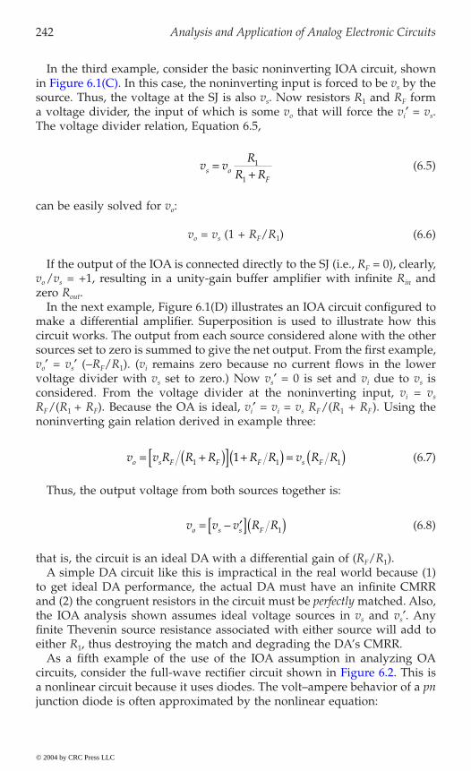
242 Analysis and Application of Analog Electronic Circuits
In the third example, consider the basic noninverting IOA circuit, showns
source. Thus, the voltage at the SJ is also vs. Now resistors R1 and RF forma voltage divider, the input of which is some vo that will force the vi¢ = vs.The voltage divider relation, Equation 6.5,
(6.5)
can be easily solved for vo:
vo = vs (1 + RF/R1) (6.6)
If the output of the IOA is connected directly to the SJ (i.e., RF = 0), clearly,vo /vs = +1, resulting in a unity-gain buffer amplifier with infinite Rin andzero Rout.
In the next example, Figure 6.1(D) illustrates an IOA circuit configured tomake a differential amplifier. Superposition is used to illustrate how thiscircuit works. The output from each source considered alone with the othersources set to zero is summed to give the net output. From the first example,vo¢ = vs¢ (-RF/R1). (vi remains zero because no current flows in the lowervoltage divider with vs set to zero.) Now vs¢ = 0 is set and vi due to vs isconsidered. From the voltage divider at the noninverting input, vi = vs
RF/(R1 + RF). Because the OA is ideal, vi¢ = vi = vs RF/(R1 + RF). Using thenoninverting gain relation derived in example three:
(6.7)
Thus, the output voltage from both sources together is:
(6.8)
that is, the circuit is an ideal DA with a differential gain of (RF/R1). A simple DA circuit like this is impractical in the real world because (1)
to get ideal DA performance, the actual DA must have an infinite CMRRand (2) the congruent resistors in the circuit must be perfectly matched. Also,the IOA analysis shown assumes ideal voltage sources in vs and vs¢. Anyfinite Thevenin source resistance associated with either source will add toeither R1, thus destroying the match and degrading the DA’s CMRR.
As a fifth example of the use of the IOA assumption in analyzing OA
a nonlinear circuit because it uses diodes. The volt–ampere behavior of a pnjunction diode is often approximated by the nonlinear equation:
v vR
R Rs oF
=+
1
1
v v R R R R R v R Ro s F F F s F= +( )[ ] +( ) = ( )1 1 11
v v v R Ro s s F= - ¢[ ]( )1
© 2004 by CRC Press LLC
in Figure 6.1(C). In this case, the noninverting input is forced to be v by the
circuits, consider the full-wave rectifier circuit shown in Figure 6.2. This is
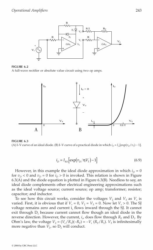
Operational Amplifiers 243
(6.9)
However, in this example the ideal diode approximation in which iD = 0for vD < 0 and vD = 0 for iD > 0 is invoked. This relation is shown in Figure6.3(A) and the diode equation is plotted in Figure 6.3(B). Needless to say, anideal diode complements other electrical engineering approximations suchas the ideal voltage source; current source; op amp; transformer; resistor;capacitor; and inductor.
To see how this circuit works, consider the voltages V2 and V3 as Vs isvaried. First, it is obvious that if Vs = 0, V2 = V3 = 0. Now let Vs > 0. The SJvoltage remains zero and current is flows inward through the SJ. It cannotexit through D1 because current cannot flow though an ideal diode in thereverse direction. However, the current, is, does flow through RF and D1. ByOhm’s law, the voltage V2 = (Vs/R1)(-RF) = -Vs (RF/R1). V3 is infinitesimallymore negative than V2, so D2 will conduct.
FIGURE 6.2A full-wave rectifier or absolute value circuit using two op amps.
FIGURE 6.3(A) I–V curve of an ideal diode. (B) I–V curve of a practical diode in which iD = Irs[exp(vD/vT) - 1].
R
R
R
R/2 RF
Vo
D1
V3
D2 V2
Vs
+OA1 OA2
Vs
0.6 V00
Vd
Vd
+
−
Id > 0Id Id
Vd Irs
A B
i I v VD RS D T= ( ) -[ ]exp h 1
© 2004 by CRC Press LLC
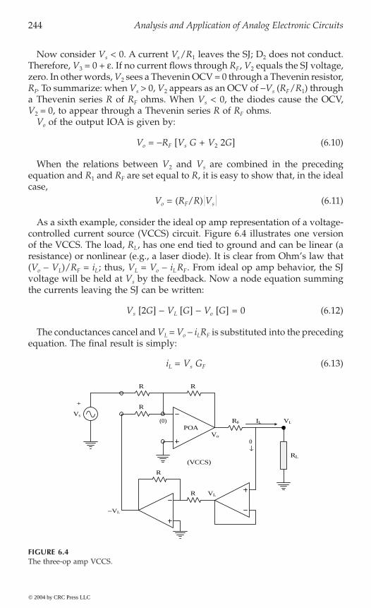
244 Analysis and Application of Analog Electronic Circuits
Now consider Vs < 0. A current Vs/R1 leaves the SJ; D2 does not conduct.Therefore, V3 = 0 + e. If no current flows through RF, V2 equals the SJ voltage,zero. In other words, V2 sees a Thevenin OCV = 0 through a Thevenin resistor,RF. To summarize: when Vs > 0, V2 appears as an OCV of -Vs (RF/R1) througha Thevenin series R of RF ohms. When Vs < 0, the diodes cause the OCV,V2 = 0, to appear through a Thevenin series R of RF ohms.
Vo of the output IOA is given by:
Vo = -RF [Vs G + V2 2G] (6.10)
When the relations between V2 and Vs are combined in the precedingequation and R1 and RF are set equal to R, it is easy to show that, in the idealcase,
Vo = (RF/R) Vs (6.11)
As a sixth example, consider the ideal op amp representation of a voltage-controlled current source (VCCS) circuit. Figure 6.4 illustrates one versionof the VCCS. The load, RL, has one end tied to ground and can be linear (aresistance) or nonlinear (e.g., a laser diode). It is clear from Ohm’s law that(Vo - VL)/RF = iL; thus, VL = Vo - iL RF. From ideal op amp behavior, the SJvoltage will be held at Vs by the feedback. Now a node equation summingthe currents leaving the SJ can be written:
Vs [2G] - VL [G] - Vo [G] = 0 (6.12)
The conductances cancel and VL = Vo - iLRF is substituted into the precedingequation. The final result is simply:
iL = Vs GF (6.13)
FIGURE 6.4The three-op amp VCCS.
R R
R
R
RF VL
R VL
Vo
RL
(0)Vs
(VCCS)
POA
↓0
IL
−VL
+
© 2004 by CRC Press LLC

Operational Amplifiers 245
The transconductance of the VCCS is simply GF of the feedback resistor.Note that the unity-gain buffer is used so that all of iL flows into RL to ground.(This is especially important if RL is a glass micropipette electrode with RL
on the order of hundreds of megohms.) The inverting IOA3 is required sothat the voltage difference across RF is sensed to give current feedback. IOA1
supplying iL in a practical VCCS of this architecture can be a high-voltageoutput type or a power op amp if high iL is required.
Many more examples of IOA circuits can be considered. A number of themare included in this chapter’s home problems.
6.2 Practical Op Amps
6.2.1 Introduction
Practical op amps are characterized by a set of parameters that describe theiroutput dc drift, output noise, and signal-conditioning properties such asdynamic range, frequency response, and slew rate. These parameters aregenerally given by manufacturers on device data sheets; they include:
• Input offset voltage (Vos)• Input bias currents (IB, IB¢ )• Input equivalent short-circuit voltage noise (ena)• Input equivalent current noise (ina)• dc Differential gain (Kv)• GBWP• Unity gain• -3-dB frequency (fT)• Lowest open-loop break frequency (fb)• Output voltage slew rate (h V/ms)• CMRR• Rin
• Ro
The following sections examine how a practical OA’s parameters determineits behavior.
6.2.2 Functional Categories of Real Op Amps
Engineers and manufacturers group op amps into functional categories, eachof which has a set of unique features that makes it suitable for a uniquedesign application. Examples of these categories are described next.
© 2004 by CRC Press LLC
246 Analysis and Application of Analog Electronic Circuits
Low noise. Signal conditioning system design with low-noise op amps inthe headstage is mandatory for maximum SNRout. Low-noise op amps arecharacterized by low values of the equivalent short-circuit input voltagenoise, ena nVRMS/÷Hz. In the author’s experience, any op amp with an ena <8 nVRMS/÷Hz should be categorized as low noise. Some op amps with FETinput transistors (head stages) have exceptionally low equivalent input cur-rent noise, ina, as well as low ena. However, some of the lowest-noise op ampshave BJT head stages and boast ena in the order of 1 nVRMS/÷Hz. For exam-ple, the venerable OP-27 op amp has ena = 3.1 nV/÷Hz and ina = 1 pA/÷Hzat 30 Hz. It uses BJT head-stage architecture and has IB = 12 nA.
Electrometer op amps. The two salient properties of electrometer amplifiersare their ultra-low dc bias currents and their extra-high input resistances.For example, the AD549 is an electrometer-grade JFET head-stage OA. Its IB
is rated from 60 to 200 fA (10-15 A), but in selected units can approach ±10fA. Rin is on the order of 1013 to 1014 W, ena = 35 nV/÷Hz, and ina =0.16 fARMS/÷Hz at 1 kHz. Electrometer op amps are used to design signalconditioning systems for pH meter glass electrodes and for intracellular glassmicropipette electrodes in which source impedances can be as high as 109 W.
Chopper-stabilized op amps. This class of op amp is used to condition dcsignals from devices such as strain gauge bridges (used in blood pressuresensors) and in any measurement system in which the QUM is essentially dcand minimizing long-term dc drift on the output of the analog signal condi-tioning system is desired. The internal chopper circuitry gives this class of OAan exceptional high dc voltage gain, on the order of 108. The net effect of thishigh gain is to minimize the effect of Vos and Vos drift with temperature change.
Another approach to canceling the effect of Vos drift in op amps used indc signal conditioning applications is offered by National Semiconductor.The LMC669 auto-zero module can be used with any op amp configured asa single-ended inverting summer or as a simple noninverting amplifier. Notethat the auto-zero module does not limit the dynamic performance of theop amp circuit to which it is attached; the amplifier retains the same dc gain,small-signal bandwidth, and slew rate. The effective offset voltage drift ofany op amp using the auto-zero is approximately 100 nV/∞C. The maximumoffset voltage using the auto-zero is ±5 mV. The auto-zero’s bias currents areapproximately 5 pA (and must be added to the op amp’s IB in the invertingarchitecture); its clock frequency can be set from 100 Hz to 100 kHz.
The LMC669 auto-zero module is very useful to compensate for dc driftin circuits using special-purpose op amps such as electrometers, which nor-mally have large offset voltages (200 mV) and large Vos tempcos (5 mV/∞C).The auto-zero does contribute to an increase in the circuit’s equivalent inputvoltage noise. However, choice of sampling rate and step size, as well as theuse of low-pass filtering in the feedback path, can minimize this effect.Application circuits are illustrated in Section 2.4.3 in Northrop (1997).
Wide-band and high slew rate op amps. Wide-band and high slew-rateop amps are used for conditioning signals such as ultrasound (CW andpulsed) at frequencies in the tens of megahertz, as well as pulsed signals
© 2004 by CRC Press LLC
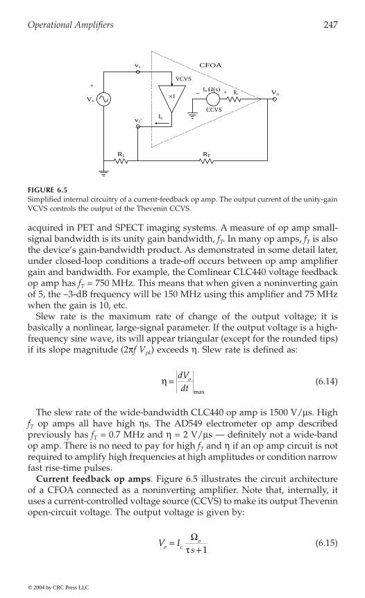
Operational Amplifiers 247
acquired in PET and SPECT imaging systems. A measure of op amp small-signal bandwidth is its unity gain bandwidth, fT. In many op amps, fT is alsothe device’s gain-bandwidth product. As demonstrated in some detail later,under closed-loop conditions a trade-off occurs between op amp amplifiergain and bandwidth. For example, the Comlinear CLC440 voltage feedbackop amp has fT = 750 MHz. This means that when given a noninverting gainof 5, the -3-dB frequency will be 150 MHz using this amplifier and 75 MHzwhen the gain is 10, etc.
Slew rate is the maximum rate of change of the output voltage; it isbasically a nonlinear, large-signal parameter. If the output voltage is a high-frequency sine wave, its will appear triangular (except for the rounded tips)if its slope magnitude (2pf Vpk) exceeds h. Slew rate is defined as:
(6.14)
The slew rate of the wide-bandwidth CLC440 op amp is 1500 V/ms. HighfT op amps all have high hs. The AD549 electrometer op amp describedpreviously has fT = 0.7 MHz and h = 2 V/ms — definitely not a wide-bandop amp. There is no need to pay for high fT and h if an op amp circuit is notrequired to amplify high frequencies at high amplitudes or condition narrowfast rise-time pulses.
Current feedback op amps. Figure 6.5 illustrates the circuit architectureof a CFOA connected as a noninverting amplifier. Note that, internally, ituses a current-controlled voltage source (CCVS) to make its output Theveninopen-circuit voltage. The output voltage is given by:
(6.15)
FIGURE 6.5Simplified internal circuitry of a current-feedback op amp. The output current of the unity-gainVCVS controls the output of the Thevenin CCVS.
−×1+In Ω(s)
CCVS
VCVS
Invi’
RFR1
Vo
Vs
+
vi
Ro
CFOA
h =dVdt
o
max
V Iso c
o=+
Wt 1
© 2004 by CRC Press LLC
248 Analysis and Application of Analog Electronic Circuits
Wo is the CFOA dc transresistance. The input to the CFOA is a unity-gainvoltage-controlled voltage source (VCVS). The noninverting input (vi) has avery high input resistance. The resistance looking into the inverting input(vi¢) node is generally <50 W; it is the Thevenin output resistance of the unity-gain VCVS.
The output current of the VCVS, In, is determined by Kirchoff’s currentlaw (a node equation) written on the low-impedance inverting (vi¢) node.The Rout of the CCVS is also < 50 W and generally can be neglected in pencil-and-paper analysis. The CFOA has many interesting properties, which aredescribed in Section 6.4. One interesting property is that, unlike a voltage-input OA, the CFOA connected as a noninverting amplifier does not tradeoff bandwidth for closed-loop gain. Its gain can be shown to be set by R1,while its closed-loop corner frequency is set by RF. Its closed-loop dc gain is(1 + RF/R1), similar to that of a conventional noninverting voltage feedbackOA.
Power op amps. Power op amps are used as audio power amplifiers,drivers for small DC servo motors, drivers for LEDs, and laser diodes (asVCCSs). Most conventional op amps can source no more than about ±10 mA;also, their output voltages saturate at slightly below their dc supply voltages,usually no more than ±15 V. The most robust power op amps (e.g., Apex PA03)typically can source as much as ±30 A, given a supply voltage range of±15/75 V, and dissipate 500 W maximum. The PA03 has a slew rate of h =8 V/ms and fT = 1 MHz. Other POAs, such as the Apex PA85, have extraor-dinary dynamic properties: namely, Iomax = ±350 mA(peak); a supply voltagerange of ±75/600 V; a power dissipation of 40 W; a slew rate of 1000 V/ms;and fT = 100 MHz. The PA85 is well suited to drive ultrasound transducers.
6.3 Gain-Bandwidth Relations for Voltage-Feedback OAs
6.3.1 The GBWP of an Inverting Summer
The open loop op amp is assumed to have a compensated differential fre-quency response given by:
(6.16)
The gain-bandwidth product of the open-loop amplifier is:
(6.17)
V V Vo i i= - ¢( ) +K
jvo
aw t 1
GBWP Hzd voa
K= 12pt
© 2004 by CRC Press LLC
Figure 6.1(B) shows the schematic of a k-input inverting summer amplifier.
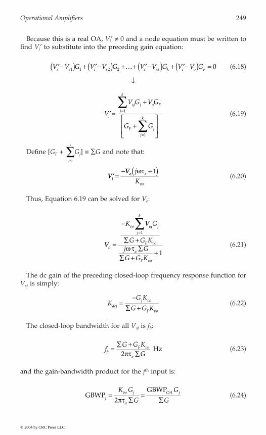
Operational Amplifiers 249
Because this is a real OA, Vi¢ π 0 and a node equation must be written tofind Vi¢ to substitute into the preceding gain equation:
(6.18)
Ø
(6.19)
Define [GF + Gj] ∫ ÂG and note that:
(6.20)
Thus, Equation 6.19 can be solved for Vo:
(6.21)
The dc gain of the preceding closed-loop frequency response function forVsj is simply:
(6.22)
The closed-loop bandwidth for all Vsj is fb:
(6.23)
and the gain-bandwidth product for the jth input is:
(6.24)
¢-( ) + ¢-( ) + º + ¢-( ) + ¢-( ) =V V G V V G V V G V V Gi s i s i sk k i o F1 1 2 2 0
¢ =
+
+È
ÎÍÍ
ù
ûúú
=
=
Â
ÂV
V G V G
G G
i
sj j o Fj
k
F jj
k
1
1
j
k
=
Â1
¢ =- +( )
VV
io j
Ka
vo
wt 1
V
V
o
sj
=
-
 +Â
 ++
=ÂK G
G G Kj GG G K
vo jj
k
F vo
a
F vo
1
1w t
KG K
G G Kdcjj vo
F vo
=-
 +
fG G K
GbF vo
a
=Â +
Â2pt Hz
GBWPGBWP
jvo j
a
OA jK G
G
G
G=
Â=
Â2pt
© 2004 by CRC Press LLC
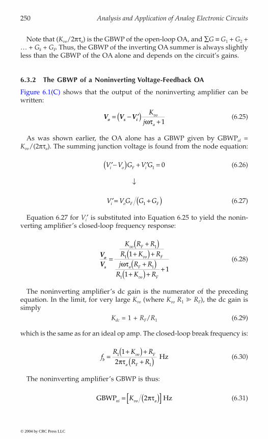
250 Analysis and Application of Analog Electronic Circuits
Note that (Kvo/2pta) is the GBWP of the open-loop OA, and ÂG ∫ G1 + G2 +… + Gk + GF. Thus, the GBWP of the inverting OA summer is always slightlyless than the GBWP of the OA alone and depends on the circuit’s gains.
6.3.2 The GBWP of a Noninverting Voltage-Feedback OA
written:
(6.25)
As was shown earlier, the OA alone has a GBWP given by GBWPol =Kvo/(2pta). The summing junction voltage is found from the node equation:
(6.26)
Ø
(6.27)
Equation 6.27 for Vi¢ is substituted into Equation 6.25 to yield the nonin-verting amplifier’s closed-loop frequency response:
(6.28)
The noninverting amplifier’s dc gain is the numerator of the precedingequation. In the limit, for very large Kvo (where Kvo R1 RF), the dc gain issimply
Kdc = 1 + RF/R1 (6.29)
which is the same as for an ideal op amp. The closed-loop break frequency is:
(6.30)
The noninverting amplifier’s GBWP is thus:
(6.31)
V V Vo s i= - ¢( ) +K
jvo
awt 1
¢-( ) + ¢ =V V G V Gi o F i 1 0
¢ = +( )V V G G Gi o F F1
VV
o
s
=
+( )+( ) +
+( )+( ) +
+
K R R
R K R
j R R
R K R
vo F
vo F
a F
vo F
1
1
1
1
1
11
wt
fR K R
R Rbvo F
a F
=+( ) +
+( )1
1
12pt
Hz
GBWP Hzni vo aK= ( )[ ]2pt
© 2004 by CRC Press LLC
Figure 6.1(C) shows that the output of the noninverting amplifier can be

Operational Amplifiers 251
Therefore, GBWPni is the same as the op amp and is independent of gain.Thus, an ideal hyperbolic relation exists between closed-loop -3-dB fre-quency (fbcl) and closed-loop gain, e.g.,
(6.32)
The noninverting op amp amplifier is unique in this property.
6.4 Gain-Bandwidth Relations in Current Feedback Amplifiers
6.4.1 The Noninverting Amplifier Using a CFOA
quency response:
(6.33)
The gain-bandwidth product of the CCVS is simply Wo/(2pta) ohm Hz.A small Thevenin source resistance appears in series with Vo from the
CCVS. This Ro is RF, so it is neglected. There is also a small Thevenin Ro inseries with the VCVS at the CFOA’s input that will be neglected. A nodeequation is written at the Vi¢ node; note that
Vi¢ = Vs.
(Vs - Vo)GF + Vs G1 = Ic (6.34)
Substituting Equation 6.34 for Ic into Equation 6.33 yields:
(6.35)
Equation 6.35 is solved for the frequency response of the closed-loopsystem:
(6.36)
f K R Rbcl vo a F= ( )[ ] +( )2 1 1pt Hz
VI
o
C
=+
Wo
ajwt 1
VV V V
oa o s=
-( ) +[ ]+
G G
jF o
a
1
1
Wwt
VV
o
s
jG G G
j GF o F o
a F o
wwt
( ) =+( ) +( )
+( ) +1 1
1 1W W
W
© 2004 by CRC Press LLC
Refer to Figure 6.5. Assume that the CCVS has a transimpedance with fre-
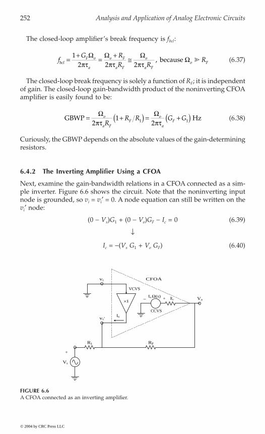
252 Analysis and Application of Analog Electronic Circuits
The closed-loop amplifier’s break frequency is fbcl:
(6.37)
The closed-loop break frequency is solely a function of RF; it is independentof gain. The closed-loop gain-bandwidth product of the noninverting CFOAamplifier is easily found to be:
(6.38)
Curiously, the GBWP depends on the absolute values of the gain-determiningresistors.
6.4.2 The Inverting Amplifier Using a CFOA
Next, examine the gain-bandwidth relations in a CFOA connected as a sim-ple inverter. Figure 6.6 shows the circuit. Note that the noninverting inputnode is grounded, so vi = vi¢ = 0. A node equation can still be written on thevi¢ node:
(0 - Vs)G1 + (0 - Vo)GF - Ic = 0 (6.39)
Ø
Ic = -(Vs G1 + Vo GF) (6.40)
FIGURE 6.6A CFOA connected as an inverting amplifier.
fG R
R RRbcl
F o
a
o F
a F
o
a Fo F=
+=
+@
12 2 2
W W WW
pt pt pt, because
GBWP Hz= +( ) = +( )W Wo
a FF
o
aFR
R R G G2
121 1pt pt
−×1+In Ω(s)
CCVS
VCVS
Invi’
RFR1
Vo
vi
Ro
CFOA
+
Vs
© 2004 by CRC Press LLC

Operational Amplifiers 253
Equation 6.40 is substituted into Equation 6.33 to find the frequencyresponse of the closed-loop amplifier:
(6.41)
Ø
(6.42)
Again, the closed-loop break frequency depends on the size of RF:
(6.43)
The GBWP is:
(6.44)
Curiously, the closed-loop break frequency depends only on R1 and theclosed-loop dc gain is
Vo/Vs @ -RF/R1. (6.45)
6.4.3 Limitations of CFOAs
CFOAs cannot be directly substituted into most conventional voltage feed-back OA circuits. For example, consider the CFOA “integrator” circuit shown
i
Ic = (0 - Vs)G1 + (0 - Vo) jwC (6.46)
Equation 6.46 for Ic is substituted into Equation 6.33 for Vo:
(6.47)
Ø
(6.48)
V V Vo s o= - +( ) +G G
jFo
a1 1
Wwt
VV
o
s
=- +( )
+( ) +
G G
j G
o F o
a F o
1 1
1 1
W W
Wwt
fG
Rbcl
F o
a
o
a F
=+( )
@1
2 2
W Wpt pt
Hz
GBWP Hz=+( )
+( )[ ] =1
21
211
GG G
RF o
ao F o
o
a
WW W
Wpt pt
V V Vo s o= - +( ) +G j C
jo
a1 1
wwt
W
VV
o
s
=-
+( ) +G
j Co
a o
1
1W
Ww t
© 2004 by CRC Press LLC
in Figure 6.7(A); the node equation on the v ¢ node is written:

254 Analysis and Application of Analog Electronic Circuits
Clearly, Equation 6.48 is the frequency response of a low-pass filter, notthat of an operational integrator. The closed-loop time constant will be long,however. If Wo = 107 ohms and C = 10-6 F, the closed-loop time constant willbe approximately 10 sec, which means that signals with frequencies aboveapproximately 40 mHz will be “integrated.” This is a poor integrator.
By way of comparison, find the frequency response of a conventionalvoltage-feedback OA integrator. The VCVS op amp’s open-loop gain is givenby:
(6.49)
The node equation for the summing junction is:
(Vi¢ - Vs)G1 + (Vi¢ - Vo) jwC = 0 (6.50)
from which,
(6.51)
FIGURE 6.7(A) A CFOA connected as a conventional integrator. The circuit does not work. (B) Two CFOAsconnected to make a near ideal inverting integrator.
CFOA1
CFOA2
In1
In2
Vs
R1
RF
CR
Vo
vi1
+
vi2’
R
C
Vs
Vo
CFOAIn
Vi
Vi’
A
B
V Vo i= - ¢+
Kj
vo
awt 1 OLG
¢ =++
VV V
is oG j CG j C
1
1
ww
© 2004 by CRC Press LLC
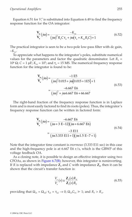
Operational Amplifiers 255
Equation 6.51 for Vi¢ is substituted into Equation 6.49 to find the frequencyresponse function for the OA integrator:
(6.52)
The practical integrator is seen to be a two-pole low-pass filter with dc gain,-Kvo.
To appreciate what happens to the integrator’s poles, substitute numericalvalues for the parameters and factor the quadratic denominator. Let R1 =106 W; C = 1 mF; Kvo = 105; and ta = 15 MS. The numerical frequency responsefunction for the integrator is found to be:
(6.53)
The right-hand fraction of the frequency response function is in Laplaceform and is most easily factored to find its roots (poles). Thus, the integrator’sfrequency response function can be written in factored form:
(6.54)
Note that the integrator time constant is enormous (3.333 E11 sec) in this caseand the high-frequency pole is at 6.667 E6 r/s, which is the GBWP of thisvoltage feedback OA.
As a closing note, it is possible to design an effective integrator using two
If R is replaced with impedance Z1 and C with impedance Z2, then it can beshown that the circuit’s transfer function is:
(6.55)
providing that Wo1 = Wo2; ta1 = ta2 Æ 0; Wo1Go1 1; and RF > RA.
VV
o
s
jK
j R C j K R Cvo
L a a vo
ww t w t
( ) =-
( ) + +( ) +21 1
VV
o
s
jj j
j j
ww w
w w
( ) = -( ) + +[ ] +
= -( ) + +
1
0 015 0 015 1 1
6 667
6 667 6 66 667
2
2
E5
E5
E6
E
. .
.
. .
VV
o
s
jj j
j j
ww w
w w
( ) = -+ -( ) +( )
= -+( ) - +( )
6 667 63 6 667 6
3 113 333 11 1 1 5 7 1
..
. .
E E 12 E
E E E
VV
ss Rs R
o
s
A
F
( ) @ ( )( )
ZZ
2
1
© 2004 by CRC Press LLC
CFOAs, as shown in Figure 6.7(B); however, this integrator is noninverting.
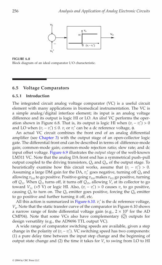
256 Analysis and Application of Analog Electronic Circuits
6.5 Voltage Comparators
6.5.1 Introduction
The integrated circuit analog voltage comparator (VC) is a useful circuitelement with many applications in biomedical instrumentation. The VC isa simple analog/digital interface element; its input is an analog voltagedifference and its output is logic HI or LO. An ideal VC performs the oper-ation shown in Figure 6.8. That is, its output is logic HI when (vi - vi¢ ) > 0and LO when (vi - vi¢) £ 0. vi or vi¢ can be a dc reference voltage, f.
An actual VC circuit combines the front end of an analog differential
gate. The differential front end can be described in terms of: difference-modegain; common-mode gain; common-mode rejection ratio; slew rate; and dc
LM311 VC. Note that the analog DA front end has a symmetrical push–pulloutput coupled to the driving transistors, Q8 and Q9, of the output stage. Toheuristically examine how this circuit works, assume that (vi - vi¢ ) > 0.Assuming a large DM gain for the DA, vo¢ goes negative, turning off Q8 andallowing vb10 to go positive. Positive-going vb10 makes vb11 go positive, turningoff Q11. When Q11 turns off, it turns off Q15, allowing Vo at its collector to gotoward VLL (+5 V) or logic HI. Also, (vi - vi¢ ) > 0 causes vo to go positive,causing Q9 to turn on. The Q9 emitter goes positive, forcing the Q8 emitterto go positive and further turning it off, etc.
i
Vf. Note that the static transfer curve of the comparator in Figure 6.10 showsa narrow range of finite differential voltage gain (e.g., 2 ¥ 105 for the ADCMP04). Note that some VCs also have complementary (Q) outputs fordesign versatility (e.g., the AD9696 TTL output VC).
A wide range of comparator switching speeds are available, given a stepchange in the polarity of (vi - vi¢ ). VC switching speed has two components:(1) a pure delay time between the input step change and the beginning ofoutput state change and (2) the time it takes for Vo to swing from LO to HI
FIGURE 6.8Block diagram of an ideal comparator I/O characteristic.
0−(vi − vi’)
vi’
vi
HI vo
vo
© 2004 by CRC Press LLC
input offset voltage. Figure 6.9 illustrates the output stage of the well-known
All this action is summarized in Figure 6.10. v ¢ is the dc reference voltage,
amplifier (see Chapter 3) with the output stage of an open-collector logic
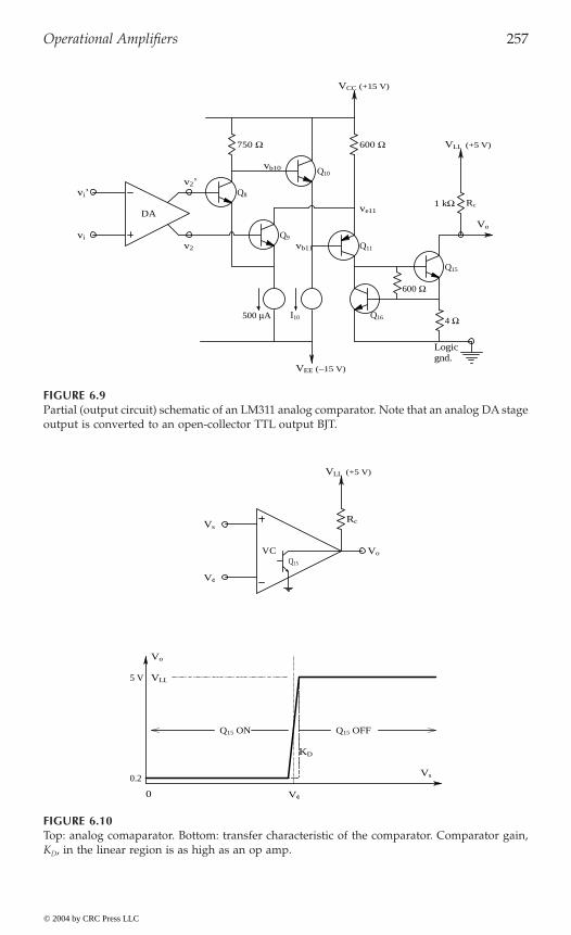
Operational Amplifiers 257
FIGURE 6.9Partial (output circuit) schematic of an LM311 analog comparator. Note that an analog DA stageoutput is converted to an open-collector TTL output BJT.
FIGURE 6.10Top: analog comaparator. Bottom: transfer characteristic of the comparator. Comparator gain,KD, in the linear region is as high as an op amp.
v2’Q8
Q10
Q9
v2 vb11 Q11
DA
vi’
vi
500 µA I10 Q16 4 Ω
600 Ω
Q15
VLL (+5 V)750 Ω 600 Ω
Logicgnd.
VCC (+15 V)
VEE (−15 V)
vb10
ve111 kΩ Rc
Vo
Q15
VLL
Vo
5 V
Vs0.2
Vφ0
VLL (+5 V)
Vo
Vφ
VsRc
Q15 OFFQ15 ON
KD
VC
© 2004 by CRC Press LLC
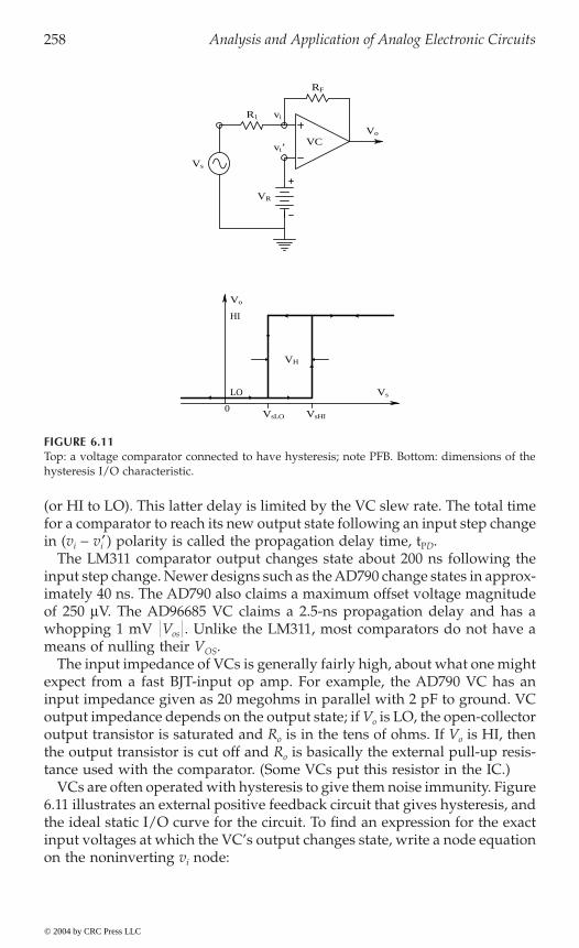
258 Analysis and Application of Analog Electronic Circuits
(or HI to LO). This latter delay is limited by the VC slew rate. The total timefor a comparator to reach its new output state following an input step changein (vi - vi¢ ) polarity is called the propagation delay time, tPD.
The LM311 comparator output changes state about 200 ns following theinput step change. Newer designs such as the AD790 change states in approx-imately 40 ns. The AD790 also claims a maximum offset voltage magnitudeof 250 mV. The AD96685 VC claims a 2.5-ns propagation delay and has awhopping 1 mV Vos . Unlike the LM311, most comparators do not have ameans of nulling their VOS.
The input impedance of VCs is generally fairly high, about what one mightexpect from a fast BJT-input op amp. For example, the AD790 VC has aninput impedance given as 20 megohms in parallel with 2 pF to ground. VCoutput impedance depends on the output state; if Vo is LO, the open-collectoroutput transistor is saturated and Ro is in the tens of ohms. If Vo is HI, thenthe output transistor is cut off and Ro is basically the external pull-up resis-tance used with the comparator. (Some VCs put this resistor in the IC.)
VCs are often operated with hysteresis to give them noise immunity. Figure6.11 illustrates an external positive feedback circuit that gives hysteresis, andthe ideal static I/O curve for the circuit. To find an expression for the exactinput voltages at which the VC’s output changes state, write a node equationon the noninverting vi node:
FIGURE 6.11Top: a voltage comparator connected to have hysteresis; note PFB. Bottom: dimensions of thehysteresis I/O characteristic.
Vo
HI
0VsHIVsLO
VsLO
VH
Vo
vi
Vs
vi’VC
RF
R1
VR
© 2004 by CRC Press LLC
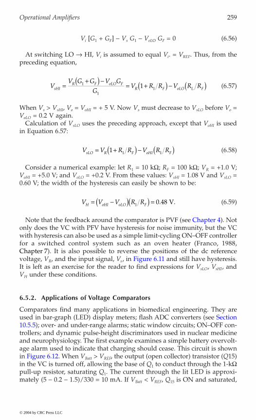
Operational Amplifiers 259
Vi [G1 + GF] - Vs G1 - VoLO GF = 0 (6.56)
At switching LO Æ HI, Vi is assumed to equal Vi. = VREF. Thus, from thepreceding equation,
(6.57)
When Vs > VsHI, Vo = VoHI = + 5 V. Now Vs must decrease to VsLO before Vo =VoLO = 0.2 V again.
Calculation of VsLO uses the preceding approach, except that VoHI is usedin Equation 6.57:
(6.58)
Consider a numerical example: let R1 = 10 kW; RF = 100 kW; VR = +1.0 V;VoHI = +5.0 V; and VoLO = +0.2 V. From these values: VsHI = 1.08 V and VsLO =0.60 V; the width of the hysteresis can easily be shown to be:
(6.59)
only does the VC with PFV have hysteresis for noise immunity, but the VCwith hysteresis can also be used as a simple limit-cycling ON–OFF controllerfor a switched control system such as an oven heater (Franco, 1988,
R s
It is left as an exercise for the reader to find expressions for VsLO, VsHI, andVH under these conditions.
6.5.2. Applications of Voltage Comparators
Comparators find many applications in biomedical engineering. They are
trollers; and dynamic pulse-height discriminators used in nuclear medicineand neurophysiology. The first example examines a simple battery overvolt-age alarm used to indicate that charging should cease. This circuit is shown
Batt > VREF, the output (open collector) transistor (Q15)in the VC is turned off, allowing the base of Q1 to conduct through the 1-kWpull-up resistor, saturating Q1. The current through the lit LED is approxi-mately (5 - 0.2 - 1.5)/330 = 10 mA. If VBatt < VREF, Q15 is ON and saturated,
VV G G V G
GV R R V R RsHI
R F oLO FR F oLO L F=
+( ) -= +( ) - ( )1
111
V V R R V R RsLO R F oHI F= +( ) - ( )1 1 1
V V V R RH oHI oLO F= -( )( ) =1 0 48. V.
© 2004 by CRC Press LLC
voltage, V , and the input signal, V , in Figure 6.11 and still have hysteresis.
in Figure 6.12. When V
Note that the feedback around the comparator is PVF (see Chapter 4). Not
used in bar-graph (LED) display meters; flash ADC converters (see Section10.5.5); over- and under-range alarms; static window circuits; ON–OFF con-
Chapter 7). It is also possible to reverse the positions of the dc reference

260 Analysis and Application of Analog Electronic Circuits
pulling the base of Q1 down to approximately 0.2 V, keeping it off and theLED unlit.
The second example of the use of VCs is a static window comparator circuitthat lights an LED while the input voltage falls in a certain range, or window,of values. The circuit is shown in Figure 6.13. Note that tying the two opencollector output transistors together to a common pull-up resistor effectivelymakes an AND gate. Both comparator outputs must be HI (Q15L AND Q15H
are cut off) to light the LED. If either Q15 is ON, the base of Q1 is pulleddown to that Q15’s Vcsat and Q1 is cut off.
In a third and final example of using VCs, examine a simple nerve spikepulse-height discriminator designed by the author. This circuit is designedto be used in neurophysiological recording; it selects only those nerve
FIGURE 6.12A comparator circuit that will light an LED when VBatt > VREF. If VBatt < VREF, then Q15 of thecomparator is on and saturated, pulling Q1’s base low and turning it and the LED off.
FIGURE 6.13A comparator voltage range window that turns the LED on when Vs lies between VfLO and VfHI .
VREF
VBatt
1 kΩ 330Ω
hν
VLL (+5 V)
LED
Q1VC
Q15
VφLO
VφHI
VLL (+5 V)
1 kΩ 330Ω
LED ON
LED OFF Vs
VφHIQ15L0 VφLO
LED OFF
VsQ15L ON,Q15H OFF
Q15L OFF,Q15H ON
Q15H & Q15L OFF
VC
VC
Q1
ICQ15H IC
© 2004 by CRC Press LLC
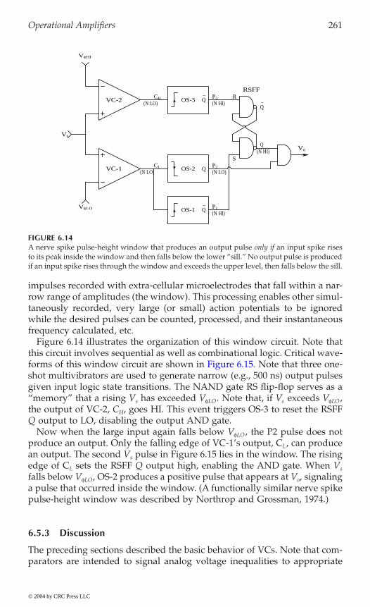
Operational Amplifiers 261
impulses recorded with extra-cellular microelectrodes that fall within a nar-row range of amplitudes (the window). This processing enables other simul-taneously recorded, very large (or small) action potentials to be ignoredwhile the desired pulses can be counted, processed, and their instantaneousfrequency calculated, etc.
Figure 6.14 illustrates the organization of this window circuit. Note thatthis circuit involves sequential as well as combinational logic. Critical wave-
shot multivibrators are used to generate narrow (e.g., 500 ns) output pulsesgiven input logic state transitions. The NAND gate RS flip-flop serves as a“memory” that a rising Vs has exceeded VfLO. Note that, if Vs exceeds VfLO,the output of VC-2, CH, goes HI. This event triggers OS-3 to reset the RSFFQ output to LO, disabling the output AND gate.
Now when the large input again falls below VfLO, the P2 pulse does notproduce an output. Only the falling edge of VC-1’s output, CL, can producean output. The second Vs pulse in Figure 6.15 lies in the window. The risingedge of CL sets the RSFF Q output high, enabling the AND gate. When Vs
falls below VfLO, OS-2 produces a positive pulse that appears at Vo, signalinga pulse that occurred inside the window. (A functionally similar nerve spikepulse-height window was described by Northrop and Grossman, 1974.)
6.5.3 Discussion
The preceding sections described the basic behavior of VCs. Note that com-parators are intended to signal analog voltage inequalities to appropriate
FIGURE 6.14A nerve spike pulse-height window that produces an output pulse only if an input spike risesto its peak inside the window and then falls below the lower “sill.” No output pulse is producedif an input spike rises through the window and exceeds the upper level, then falls below the sill.
VφHI
_Q
VC-1 QOS-2
OS-3_QVC-2 R
RSFF
S
(N LO)
(N LO)CL
CH
(N HI)P3
OS-1(N HI)
(N LO)P2
VφLO P1
(N HI)
Vs
Vo
_Q
Q
© 2004 by CRC Press LLC
forms of this window circuit are shown in Figure 6.15. Note that three one-
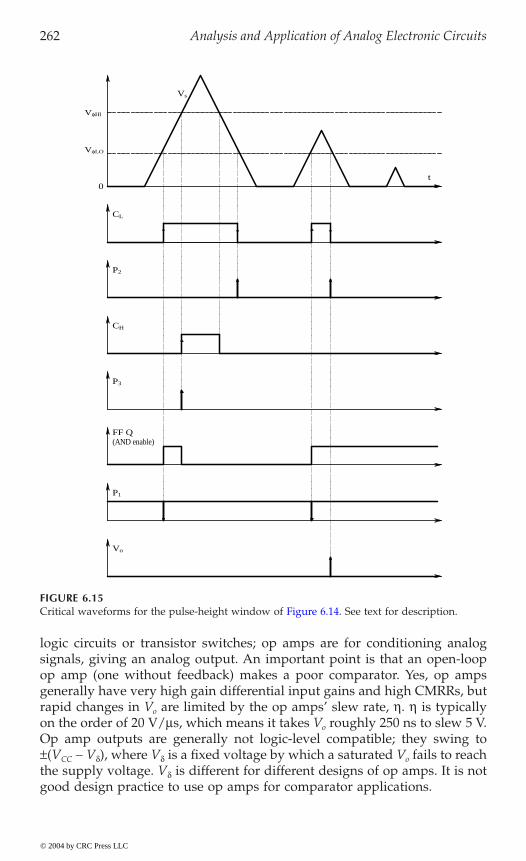
262 Analysis and Application of Analog Electronic Circuits
logic circuits or transistor switches; op amps are for conditioning analogsignals, giving an analog output. An important point is that an open-loopop amp (one without feedback) makes a poor comparator. Yes, op ampsgenerally have very high gain differential input gains and high CMRRs, butrapid changes in Vo are limited by the op amps’ slew rate, h. h is typicallyon the order of 20 V/ms, which means it takes Vo roughly 250 ns to slew 5 V.Op amp outputs are generally not logic-level compatible; they swing to±(VCC - Vd), where Vd is a fixed voltage by which a saturated Vo fails to reachthe supply voltage. Vd is different for different designs of op amps. It is notgood design practice to use op amps for comparator applications.
FIGURE 6.15
VφLO
VφHI
0
Vs
CL
P2
CH
P3
P1
(AND enable)
Vo
t
FF Q
© 2004 by CRC Press LLC
Critical waveforms for the pulse-height window of Figure 6.14. See text for description.
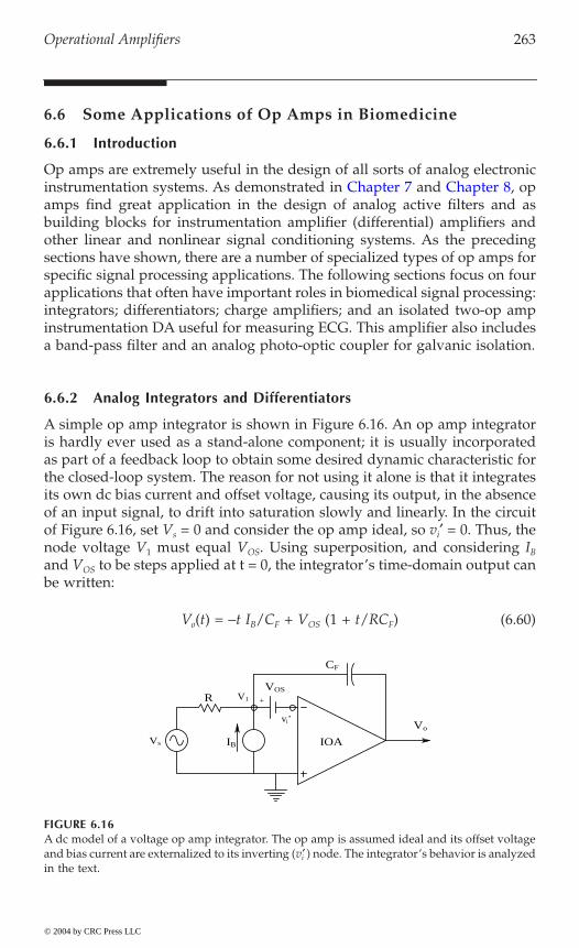
Operational Amplifiers 263
6.6 Some Applications of Op Amps in Biomedicine
6.6.1 Introduction
Op amps are extremely useful in the design of all sorts of analog electronic
amps find great application in the design of analog active filters and asbuilding blocks for instrumentation amplifier (differential) amplifiers andother linear and nonlinear signal conditioning systems. As the precedingsections have shown, there are a number of specialized types of op amps forspecific signal processing applications. The following sections focus on fourapplications that often have important roles in biomedical signal processing:integrators; differentiators; charge amplifiers; and an isolated two-op ampinstrumentation DA useful for measuring ECG. This amplifier also includesa band-pass filter and an analog photo-optic coupler for galvanic isolation.
6.6.2 Analog Integrators and Differentiators
A simple op amp integrator is shown in Figure 6.16. An op amp integratoris hardly ever used as a stand-alone component; it is usually incorporatedas part of a feedback loop to obtain some desired dynamic characteristic forthe closed-loop system. The reason for not using it alone is that it integratesits own dc bias current and offset voltage, causing its output, in the absenceof an input signal, to drift into saturation slowly and linearly. In the circuitof Figure 6.16, set Vs = 0 and consider the op amp ideal, so vi¢ = 0. Thus, thenode voltage V1 must equal VOS. Using superposition, and considering IB
and VOS to be steps applied at t = 0, the integrator’s time-domain output canbe written:
Vo(t) = -t IB/CF + VOS (1 + t/RCF) (6.60)
FIGURE 6.16A dc model of a voltage op amp integrator. The op amp is assumed ideal and its offset voltageand bias current are externalized to its inverting (vi¢ ) node. The integrator’s behavior is analyzedin the text.
IOAIB
VOS
+R
Vo
CF
Vs
vi’
V1
© 2004 by CRC Press LLC
instrumentation systems. As demonstrated in Chapter 7 and Chapter 8, op
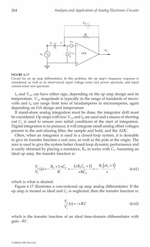
264 Analysis and Application of Analog Electronic Circuits
IB and VOS can have either sign, depending on the op amp design and itstemperature. VOS magnitude is typically in the range of hundreds of micro-volts and IB can range from tens of faradamperes to microamperes, againdepending on OA design and temperature.
If stand-alone analog integration must be done, the integrator drift mustbe considered. Op amps with low VOS and IB are used and a means of shortingout CF is used to ensure zero initial conditions at the start of integration.Digital integration is no panacea; it will integrate small analog offset voltagespresent in the anti-aliasing filter, the sample and hold, and the ADC.
Often, when an integrator is used in a closed-loop system, it is desirableto give its transfer function a real zero, as well as the pole at the origin. Thezero is used to give the system better closed-loop dynamic performance andis easily obtained by placing a resistance, RF, in series with CF. Assuming anideal op amp, the transfer function is:
(6.61)
which is what is desired.Figure 6.17 illustrates a conventional op amp analog differentiator. If the
op amp is treated as ideal and CF is neglected, then the transfer function is:
(6.62)
which is the transfer function of an ideal time-domain differentiator withgain -RC.
FIGURE 6.17Circuit for an op amp differentiator. In this problem, the op amp’s frequency response isconsidered, as well as its short-circuit input voltage noise root power spectrum, and inputcurrent noise root spectrum.
C
CF
VoOAina
ena
R
Vs
vi’
VV
sR sC
R
sR C
sRC
K s
so
s
F F F F
F
i f( ) = - + = -+( ) = -
+( )1 1 1t
VV
s sRCo
s
( ) = -
© 2004 by CRC Press LLC
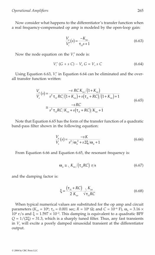
Operational Amplifiers 265
Now consider what happens to the differentiator’s transfer function whena real frequency-compensated op amp is modeled by the open-loop gain:
(6.63)
Now the node equation on the Vi¢ node is:
Vi¢ (G + s C) - Vo G = Vs s C (6.64)
Using Equation 6.63, Vi¢ in Equation 6.64 can be eliminated and the over-all transfer function written:
(6.65)
Note that Equation 6.65 has the form of the transfer function of a quadraticband-pass filter shown in the following equation:
(6.66)
From Equation 6.66 and Equation 6.65, the resonant frequency is:
(6.67)
and the damping factor is:
(6.68)
When typical numerical values are substituted for the op amp and circuitparameters (Kvo = 106; tA = 0.001 sec; R = 106 W; and C = 10-6 F), wn = 3.16 ¥104 r/s and x = 1.597 ¥ 10-2. This damping is equivalent to a quadratic BPFQ = 1/(2x) = 31.3, which is a sharply tuned filter. Thus, any fast transientsin Vs will excite a poorly damped sinusoidal transient at the differentiatoroutput.
VV
sKs
o
i
vo
A¢( ) =
-+t 1
VV
ss RC K K
s RC K s RC K
sRCs RC K s RC K
o
s
vo vo
A vo A vo
A vo A vo
( ) =- +( )
+( ) + +( ) +( ) +
@ -+ +( ) +
11 1 1
1
2
2
t t
t t
VV
ssK
s so
s n n
( ) = -+ +2 2 2 1w x w
w tn vo AK RC@ ( ) r s
xt
t=
+( )÷
A
vo
vo
A
RC
K
K
RC2
© 2004 by CRC Press LLC
266 Analysis and Application of Analog Electronic Circuits
Another problem with the simple R–C differentiator is the differentiationof the op amp’s short-circuit equivalent voltage noise, ena. The transfer func-tion for ena is easily shown to be:
Vo = Ena (1 + s RC) (6.69)
Because ena has a broadband spectrum, the differentiator’s output noisehas a spectrum that increases with frequency, making the output very noisy.(Note that the ina component in Vo is not differentiated.) When a feedbackcapacitor, CF, is added in parallel with R, the differentiator’s frequencyresponse is found from the new node equation:
(6.70)
Using Equation 6.63, Vi¢ in the preceding equation can be eliminated andthe transfer function written:
(6.71)
The differentiator transfer function still has the format of a BPF. Examineits wn and damping: all parameters are the same as the preceding ones andCF = 6.7 ¥ 10-11 F (67 pF).
(6.72)
Ø
wn = 3.1622 ¥ 104 r/s (6.73)
The damping factor is now found from:
(6.74)
(6.75)
The wn has changed little, but now the system is slightly overdamped, i.e.,both poles are close on the real axis in the s-plane. The differentiator’sfrequency response is still band pass with its peak gain at the same frequency,
¢ + +( )[ ] - +( ) =V G s C C V G sC V sCi F o F s
VV
ssRC
s R C C K s RC K RCo
s A F vo A vo F
( ) = -+( ) + +( ) +[ ] +2 1t t
wtn
vo
A F
KR C C
26
3 6 6 11810
10 10 10 6 7 109 99933 10=
+( ) =¥ ¥ + ¥( ) = ¥- - -.
.
2x w tn
A
voF
RCK
RC= + +
x = ¥ ¥ + + ¥ ¥ÊËÁ
=
--0 5 3 1622 10
10 110
6 7 10 10 1 07543
611 6. . . .
© 2004 by CRC Press LLC
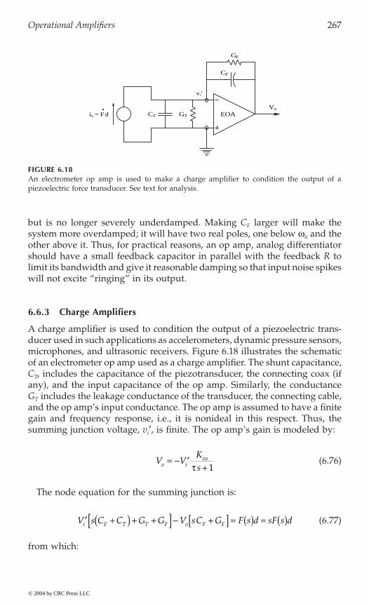
Operational Amplifiers 267
but is no longer severely underdamped. Making CF larger will make thesystem more overdamped; it will have two real poles, one below wn and theother above it. Thus, for practical reasons, an op amp, analog differentiatorshould have a small feedback capacitor in parallel with the feedback R tolimit its bandwidth and give it reasonable damping so that input noise spikeswill not excite “ringing” in its output.
6.6.3 Charge Amplifiers
A charge amplifier is used to condition the output of a piezoelectric trans-ducer used in such applications as accelerometers, dynamic pressure sensors,microphones, and ultrasonic receivers. Figure 6.18 illustrates the schematicof an electrometer op amp used as a charge amplifier. The shunt capacitance,CT, includes the capacitance of the piezotransducer, the connecting coax (ifany), and the input capacitance of the op amp. Similarly, the conductanceGT includes the leakage conductance of the transducer, the connecting cable,and the op amp’s input conductance. The op amp is assumed to have a finitegain and frequency response, i.e., it is nonideal in this respect. Thus, thesumming junction voltage, vi¢, is finite. The op amp’s gain is modeled by:
(6.76)
The node equation for the summing junction is:
(6.77)
from which:
FIGURE 6.18An electrometer op amp is used to make a charge amplifier to condition the output of apiezoelectric force transducer. See text for analysis.
vi’
GTCT
GF
CF
Vo
EOA•
ix = F d
V VKso i
vo= - ¢+t 1
¢ +( ) + +[ ] - +[ ] = ( ) = ( )V s C C G G V sC G F s d sF s di F T T F o F F
© 2004 by CRC Press LLC
268 Analysis and Application of Analog Electronic Circuits
(6.78)
Ø
(6.79)
Ø
(6.80)
To put Equation 6.80 into time-constant format, divide top and bottom byKvo GF and note that certain terms in the denominator are negligibly small.Let s = jw in order to write the charge amplifier’s frequency response:
(6.81)
The frequency response function of Equation 6.81 is band pass with tworeal poles. The low-frequency one is set by the feedback R and C and is s1 @-1/(RFCF) r/s; the high-frequency pole can be shown to be approximatelys2 @ -(Kvo/t)[CF/(CF + CT)] = wT CF/(CF + CT) r/s. wT is the op amp’s radiangain-bandwidth product. For example, set Kvo = 106; t = 10-3 sec; CF = 10-9 F;CT = 10-9 F; GF = 10-10 S; and GT = 10-12 S. Now the low break frequency isat flo = 1.59 ¥ 10-2 Hz and the high break frequency is at fhi = 80 MHz, whichis adequate for conditioning 5-MHz ultrasound.
6.6.4 A Two-Op Amp ECG Amplifier
Op amps can be used to make high-gain differential amplifiers with high
The two-op amp DA was found to have a DM gain:
Vo = (Vs - Vs¢ ) 2(1 + R/RF) (6.82)
R and RF should be chosen so that the amplifier’s DM gain is 103. To usethis amplifier as an ECG system front end, it is necessary to define the ECGband pass with a high- and low-pass filter. An easy design is to cascade the
HPF is given complex-conjugate poles with an fn = 0.1 Hz and a dampingfactor of x = 0.707. Using the design formulas given in Section 7.2.2 in
1 2 1 2 n ) = 0.1,
¢ =( ) + +[ ]
+( ) + +[ ]VsF s d V sC G
s C C C Gio F F
F T T F
V s Ks F s d V sC G
s C C G Go voo F F
F T T F
t +[ ] = -( ) + +[ ]
+( ) + +[ ]1
VF
ssK d
s C C s G G C C K C K Go vo
F T F T F T vo F vo F
( ) =-
+( ) + +( ) + + +[ ] +2t t
VF
o jj d R
j C C R K j C RF
F T F vo F F
w ww t w
( ) @ -
( ) +( ) + +21
R1R2
© 2004 by CRC Press LLC
Sallen and Key high-pass and low-pass filters, as shown in Figure 6.19. The
common-mode rejection ratios, as described in Section 3.7.2 in Chapter 3.
Chapter 7, C = C = C and, for x = 0.707, R = 2 R . f = 1/(2pC

Operational Amplifiers 269
so one can solve for R1 and R2 after choosing C = 3.3 mF. A little algebra givesR2 = 3.31 ¥ 105 and R1 = 6.821 ¥ 105 W.
The parameters for the S and K LPF are found from x = ÷C2/C1 = 0.707and fn = 1/(2pR ) = 100 Hz. Clearly, C2 = 2C1 for the desired damping.Choose C1 = 0.1 mF, so C2 = 0.2 mF. Using the fn relation, R = 1.125 ¥104 W.The op amps need not be special low-noise or high fT designs, the ECG signalhas limited bandwidth, and the noise performance is set by the differentialfront end amplifier having the gain of 103.
Now that the ECG signal has been amplified and its bandwidth defined,it is necessary to consider patient galvanic isolation. One easy way to achieveisolation is to run the DA and filter op amps on isolated battery power withno ground connection common with the power line mains. A pair of 12-Vbatteries can be used with IC voltage regulators to give ±8 V to run the foursignal conditioning op amps. One cannot simply connect the output of thefilter to an oscilloscope or computer to view the ECG. The common groundfrom the oscilloscope or computer destroys patient galvanic isolation, sosome means of coupling the signal without the necessity of a commonground must be used. One means is to sample the isolated ECG and convertit with a serial output isolated ADC and then couple the digitized ECG tothe outside using a photo-optic coupler (POC). (A transformer can also beused.) The digitized ECG must then be converted to analog form with aserial input DAC in order to be viewed on an oscilloscope or be an input toa strip-chart recorder.
A simpler form of galvanic isolation that uses POCs and gives an analog
supply of the signal conditioner. The top LED in the dual POC IC is biasedon with the 3-mA dc current source, causing an average light intensity, I1o,to be emitted. The isolated conditioned ECG output, V3, causes the lightintensity to vary proportionally around the average level, I1o. The light fromLED1 is transmitted through a plastic light guide to photodiode, PD2. Anincrease in the light hitting the photojunction of PD1 causes a proportionalincrease in its (reverse) photocurrent. PD1’s increased photocurrent is thebase current of the top npn BJT, so its collector current increases, causing theinverting input of op amp OA2 to go negative and making OA2’s output gopositive. The positive increment on OA2’s output increases the current in
FIGURE 6.19A band-pass filter for electrocardiography made from cascaded Sallen and Key high-pass filterand low-pass filters.
R
C1
LPFHPF
V1
V2CR1
R2
RC2C OA O A
V3
C1C2
© 2004 by CRC Press LLC
output is shown in Figure 6.20. OA1 is run from the isolated battery power

270 Analysis and Application of Analog Electronic Circuits
LED2 above its 3-mA bias, increasing its light output and, in turn, increasingthe photocurrent in PD2. This increases the base current in its BJT, causingthe positive input of OA2 to go negative, closing a negative feedback paththat compensates for LED and PD nonlinearities. Note that the ECG groundis completely isolated from the output ground, as is the analog ECG signal,V3, from Vout. The output of the feedback POC system is taken as the voltageacross the 2 k + 3.9 k resistors.
6.7 Chapter Summary
This chapter has been all about op amps; it began by reviewing the propertiesof the ideal op amp and showing how it can be used to facilitate heuristicanalysis of op amp circuits.
Practical conventional op amps were shown to be characterized by finitefrequency-dependent difference-mode gains and finite input and outputresistances. Their inputs were also characterized by two dc bias currents, adc offset voltage, a short-circuit input noise voltage, and an input noisecurrent. The various types of op amps were described, including: high fre-quency; high slew rate; low noise; electrometer; chopper stabilized; etc.
The effects of negative voltage feedback on a closed-loop op amp amplifier’sfrequency response was described in terms of the op amp’s gain-bandwidth
FIGURE 6.20A linear analog photo-optic coupler used to provide galvanic isolation between the battery-operated ECG measurement differential amplifier and band-pass filter, and the output recordingand display systems.
© 2004 by CRC Press LLC
3 mA dc
3 mA
−15 V (main)
−15 V (main)
Ipd1
RR
R
10 k
Vout
2 k
3.9 k
OA2
OA3
HCPL-2530
− 5 V (iso)
PD1
PD2dc LED2
LED1OA1
IFB
V3

Operational Amplifiers 271
product, or unity gain frequency. The amplifier’s gain-bandwidth productwas shown to be constant for the special case of the noninverting amplifierconfiguration and to be a function of the amplifier’s gain at low gains forthe inverting amplifier configuration.
The current feedback amplifier (CFOA) was described and analyzed; in thenoninverting gain configuration. The closed-loop amplifier’s break frequencywas found to be independent of the closed-loop gain and to depend only onthe absolute value of the feedback resistance. The same situation obtains forthe inverting amplifier configuration using the CFOA. CFOAs were alsoshown to be unsuitable for integrators unless a special 2-CFOA circuit is used.
Voltage comparators were described and shown to have DA front endsand TTL or ECL logic outputs. Comparators are useful in biomedical appli-cations, including pulse height windows used in neurophysiology and innuclear medicine. Finally, applications of op amps as differentiators, inte-grators, charge amplifiers, and ECG signal conditioning were examined.
Home Problems
6.1 An Apex PA08A high-voltage power op amp is used to drive a resistiveload. This op amp can output up to ±150 mA and swing its output voltage upto ±145 V. Its slew rate is 30 V/ms. What is the maximum Hertz frequency of asinusoidal input it can amplify to get a 100-VRMS sinusoidal output withoutslew rate distortion?
6.2op amp connected as a noninverting amplifier with voltage gain (1 + RF /R1).This is an Intersil ICL7605/7606 CAZ amplifier intended for nondrifting dcamplification applications such as strain gauge bridges and electronic scales.The over-all bandwidth is made about 10 Hz. Note that the CAZ op amp hastwo matched op amps internally and a number of analog MOS switches tochange periodically its input circuitry and switch its output. Two matchedexternal capacitors are used to store dc offset voltages. Assume the two internalop amps are ideal except for their offset voltages. Describe how this circuitworks to realize an amazing overall offset voltage tempco of ±10 nV/∞C.
6.3op amp has an open-loop transfer function given by:
a. Give the Hertz gain*bandwidth product of the op amps alone.b. Find an expression for the transfer function of the cascaded am-
plifiers, (V3/V1)(s), in time-constant form.c. Give numerical values for the -3-dB frequency and the fT of the
amplifier.
VV V s
o
i i- ¢( ) =+-
1010 1
5
3
© 2004 by CRC Press LLC
Figure P6.2(A) and Figure P6.2(B) illustrate a commutating auto-zero (CAZ)
Two cascaded noninverting voltage op amps are shown in Figure P6.3. Each
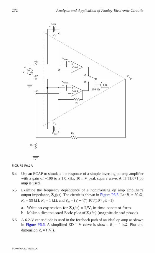
272 Analysis and Application of Analog Electronic Circuits
6.4 Use an ECAP to simulate the response of a simple inverting op amp amplifierwith a gain of -100 to a 1.0 kHz, 10 mV peak square wave. A TI TL071 opamp is used.
6.5 Examine the frequency dependence of a noninverting op amp amplifier’s
o o
RF = 99 kW; R1 = 1 kW; and Voc = (Vi - Vi¢) 104/(10-3 jw +1).
a. Write an expression for Zo(jw) = It/Vt in time-constant form.b. Make a dimensioned Bode plot of Zo(jw) (magnitude and phase).
6.6 A 6.2-V zener diode is used in the feedback path of an ideal op amp as shown
1
dimension Vo = f (V1).
FIGURE P6.2A
+−
+VOS2
−
A
OA-1
B
VOS1
Clk.
160 Hz
R2
AZ
+in
−in
RF
Vo
OA-2
C1
+VOS1
C2
+VOS2
R1
V1
+
© 2004 by CRC Press LLC
output impedance, Z (jw). The circuit is shown in Figure P6.5. Let R = 50 W;
in Figure P6.6. A simplified ZD I–V curve is shown. R = 1 kW. Plot and
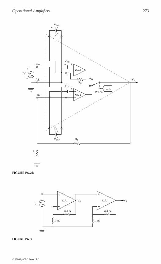
Operational Amplifiers 273
FIGURE P6.2B
FIGURE P6.3
C1
VOS1+
+
+VOS2
C2
VOS2
OA-1
OA-2
+in
−in
B
AZ A
−
−
RF
R1
Vo
+
Clk.
VOS1
160 Hz
−
+
V1
R2
99 kΩ 99 kΩ
1 kΩ 1 kΩ
V1
V3V2OA OA
© 2004 by CRC Press LLC

274 Analysis and Application of Analog Electronic Circuits
6.7 1
and RL = 1 kW. Plot and dimension several cycles of Vo(t) and V2(t). Assume
the diodes have the I–V characteristic shown.
6.8 1
are the same as in the preceding problem. Plot and dimension several cycles ofVo(t) and V2(t).
6.9 An npn BJT is used in the feedback path of an ideal op amp as shown in
by IC @ Is exp(VBE /VT), where Is is the collector saturation current = 0.25 pA;VBE is the base–emitter voltage; and VT = hkT/q @ 26 mV at room temperature.
Plot and dimension Vo = f (V1).
FIGURE P6.5
FIGURE P6.6
vi
vi’
0
RF
R1
voc
Vt
(Test source)
ItRo Vo
V1
Vo
VD
VD
R1
0.65 V
−VZ
ID
ID
IOA
+−
ZD (Zener I-V characteristic)
© 2004 by CRC Press LLC
A version of a diode bridge is shown in Figure P6.7. Assume v (t) = 1.4 sin(377t)
Another precision rectifier bridge is shown in Figure P6.8. v (t) and the diodes
Figure P6.9. The BJT is forward-biased; its collector current can be modeled
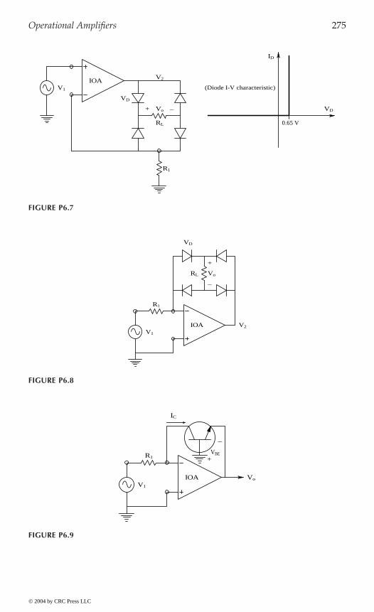
Operational Amplifiers 275
FIGURE P6.7
FIGURE P6.8
FIGURE P6.9
RL
VD
VD
R1
0.65 V
ID
IOA
Vo+ −
V1 (Diode I-V characteristic)
V2
V1
VoRL
VD
R1
IOA
+
−
V2
V1
Vo
IC
R1VBE
IOA
+
−
© 2004 by CRC Press LLC

276 Analysis and Application of Analog Electronic Circuits
6.10 A laptop computer uses a nominal 12-V battery. It is desired to design a bargraph type of LED voltmeter display that will measure the battery voltageover the range of 9 to 12 V. A partial schematic of the voltmeter is shown inFigure P6.10. An LM336 IC reference voltage chip supplies a constant 2.5 Vdcas long as VB > 6 V. The comparators also run off VB as long as VB > 6 V.Comparator 1 lights its LED when the voltage at its inverting terminal exceedsVR = 2.5 V; this makes its logic output low and allows current to flow throughits LED. The comparator 1 inverting terminal voltage is a1VB. a1 = R/(R +R1a). R ∫ 10 kW. Comparator 1’s LED lights only for VB > 12 V. Comparator 2lights its LED for VB > 11.5 V; comparator 3’s LED lights for VB > 11.0 V;comparator 4’s LED lights for VB > 10.5 V; the comparator 5 LED lights forVB > 10.0 V; comparator 6’s LED lights for VB > 9.5 V; and comparator 7’sLED lights for VB > 9.0 V. Thus, a fully charged battery will light all sevenLEDs when the button is pushed and, if 10.0 < VB < 10.5, only LEDs 5, 6, and7 will light. Calculate the necessary values of R1a through R7a required to makethe LED voltmeter work as described.
6.11resistance circuit. Find an algebraic expression for the input admittance, Gin =Is /Vs S. Assume that Vo = Vs (1 + RF /R1) for the amplifier. Assume that Ri andRcm RF and R1. Evaluate Gin numerically: let Ri = 10 MW; Rcm = 400 MW;
and RF = R1 = 3.3 kW.
6.12time-constant form. The op amp is ideal.
6.13
s
FIGURE P6.10
. . .
. . .
LM336
VR = 2.5 V
R
1 kΩ1 kΩ1 kΩR1a R2a R3a
COM1 COM2 COM3
VB
VBVR
VR
ON forVB > 12 V
ON forVB > 11.5 V
ON forVB > 11.0 V
3.3 kΩ
LED LED LED
N.O. PB
R R
© 2004 by CRC Press LLC
Figure P6.11 shows a noninverting op amp amplifier and its equivalent input
Find an expression for the transfer function of the filter of Figure P6.12 in
Find an expression for the frequency response function of the filter of FigureP6.13 in time-constant form. What function does this circuit perform on V ?
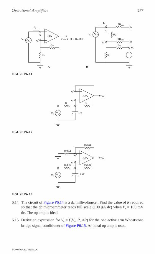
Operational Amplifiers 277
6.14so that the dc microammeter reads full scale (100 mA dc) when Vs = 100 mV
dc. The op amp is ideal.
6.15 Derive an expression for Vo = f (Vs, R, DR) for the one active arm Wheatstone
FIGURE P6.11
FIGURE P6.12
FIGURE P6.13
Vo
RR
Vs C
IOA
vi
vi’
VoIOA
vi
vi’
1 µF
15 kΩ
15 kΩ
10 kΩ
10 kΩ
Vs
© 2004 by CRC Press LLC
The circuit of Figure P6.14 is a dc millivoltmeter. Find the value of R required
bridge signal conditioner of Figure P6.15. An ideal op amp is used.
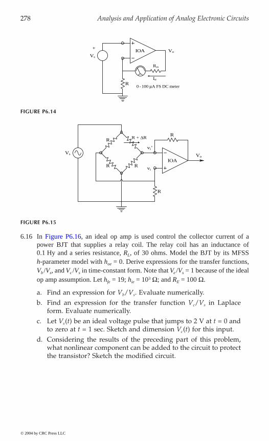
278 Analysis and Application of Analog Electronic Circuits
6.16power BJT that supplies a relay coil. The relay coil has an inductance of0.1 Hy and a series resistance, RL, of 30 ohms. Model the BJT by its MFSSh-parameter model with hoe = 0. Derive expressions for the transfer functions,Vb /Vs, and Vc /Vs in time-constant form. Note that Ve /Vs = 1 because of the idealop amp assumption. Let hfe = 19; hie = 103 W; and RE = 100 W.
a. Find an expression for Vb/Vs. Evaluate numerically.b. Find an expression for the transfer function Vc/Vs in Laplace
form. Evaluate numerically.c. Let Vs(t) be an ideal voltage pulse that jumps to 2 V at t = 0 and
to zero at t = 1 sec. Sketch and dimension Vc(t) for this input.d. Considering the results of the preceding part of this problem,
what nonlinear component can be added to the circuit to protectthe transistor? Sketch the modified circuit.
FIGURE P6.14
FIGURE P6.15
IOA
Rm
Im
Vs
+Vo
R0 - 100 µA FS DC meter
R
R
Vo
IOA
R R + ∆R
vi
Vs
vi’
R R
© 2004 by CRC Press LLC
In Figure P6.16, an ideal op amp is used control the collector current of a
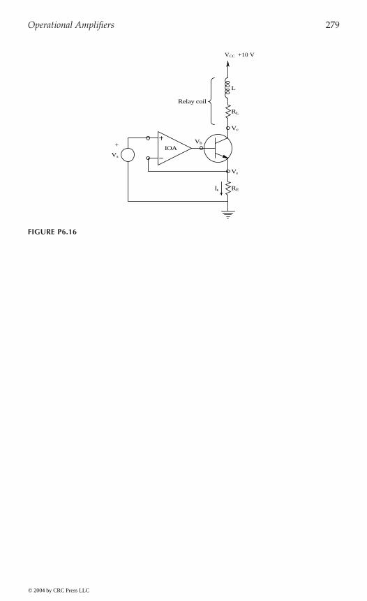
Operational Amplifiers 279
FIGURE P6.16
Vc
L
VCC +10 V
RL
Vb
Vs
IOA
Ve
REIe
Relay coil
+
© 2004 by CRC Press LLC

281
7Analog Active Filters
7.1 Introduction
Filter (noun) is an electrical engineering term having a broad definition.Filters are generally considered to operate on signals in the frequencydomain; that is, they attenuate, stop, pass, or boost certain frequency regionsin the input signal’s spectrum. These operations are called filtering (verb).They may be classified as low pass (LP); band pass (BP); high pass (HP); orband reject (BR or notch). Band-pass and band-reject filters can have narrow-pass bands or reject bands. One descriptor of such sharply tuned filters istheir Q, which can be defined as the BP filter’s center frequency divided byits half-power bandwidth; the narrower the bandwidth is, the higher the Q.(Bandwidth is generally measured as the frequency span between half-power frequencies, where the filter’s frequency response function is down-3 dB or to 0.7071 times the peak pass gain.)
Filter transfer functions can be expressed in general as rational polynomi-als in the complex variable, s. The rational polynomials can be factored tofind the poles and zeros of the transfer function. The filter’s poles are theroots of the denominator polynomial; its zeros are the roots of the numeratorpolynomial. Roots are the complex values of s that make a polynomial equalzero. If the highest power of s in the denominator polynomial is n, n poleswill be in the complex s-plane. If the filter is stable (and all should be), allof the filter’s poles will lie in the left-half s-plane; however, in limiting cases,conjugate pole pairs can lie on the jw axis.
Likewise, if the highest power of s in the numerator polynomial is m, mzeros will be in the s-plane. The zeros can lie anywhere in the s-plane; ifsome lie in the right-half s-plane, the filter is called nonminimum phase. If allthe zeros lie in the left-hand s-plane, the filter is called minimum phase. Thepoles and zeros can have real values or occur in complex-conjugate pairs ofthe form, s = a ± jb, where b is nonnegative and - < a < . Conjugate zeroson the jw axis are found in notch filters. A filter’s frequency response is foundby letting s = jw in the filter’s transfer function and then finding 20 timesthe log of the magnitude of the frequency response function vs. f in Hertzand the angle of the frequency response function vector vs. f.
© 2004 by CRC Press LLC
282 Analysis and Application of Analog Electronic Circuits
Analog active filters use feedback around op amps to realize desired trans-fer functions for applications such as band-pass and low-pass filtering toimprove signal-to-noise ratios. AFs use only capacitors and resistors in theircircuits. Inductors are not used because they are generally large, heavy, andimperfect, i.e., they have significant losses from coil resistance and otherfactors. AFs are also used to realize sharp cut-off low-pass filters (LPFs) foranti-aliasing filtering of analog signals before periodic, analog-to-digital con-version (sampling). Active notch filters are often used to eliminate the coher-ent interference that accompanies ECG, EMG, and EEG signals.
Some disconcerting news is that since EEs first discovered that op ampscan be used to realize filters, a plethora of different AF design architectureshave been developed. In, fact, several excellent texts have been written onthe specialized art of active filter design (Schaumann and Van Valkenburg,2001; Lancaster, 1996; Huelsman, 1993; Deliyannis, Sun, and Fidler, 1998). Insome AF designs, filter parameters such as mid-band gain, break frequency,Q, or damping factor cannot be designed for with unique R and C compo-nents. For example, all the filter’s Rs and Cs interact, so no single componentor set of components can independently determine mid-band gain, breakfrequency, etc.
The good news is that high-order active filters are generally designed ona modular cascaded basis using certain preferred circuit architectures thatallow exact pole and zero placement in the s-plane by simple componentvalue choice. Some examples of these preferred AF architectures will beexamined, beginning with the simple controlled-source, Sallen and Key qua-dratic low-pass filter.
7.2 Types of Analog Active Filters
7.2.1 Introduction
In the AF designs described next, the op amps will be assumed to be ideal.For serious design evaluation, computer modeling must be used with opamp dynamic models. Note that a filter’s transient response can be just asimportant as its frequency response. The band-pass filtering of an ECG signalis an example of a biomedical application of an active filter that is transientresponse sensitive. The fidelity of the sharp QRS spike must be preservedfor diagnosis; there must be little rounding of the R-peak and no transient“ringing” following the QRS spike. The linear phase Bessel filter is one classof AF that is free from ringing and suitable for conditioning ECG signals.The exact position of the poles of a high-order (n > 2) Bessel filter determineits characteristics; this filter will be examined in detail later.
© 2004 by CRC Press LLC
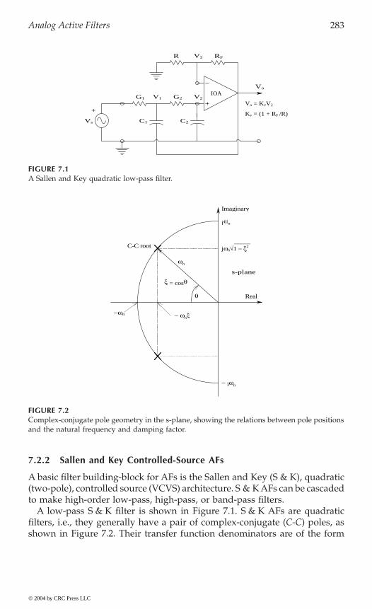
Analog Active Filters 283
7.2.2 Sallen and Key Controlled-Source AFs
A basic filter building-block for AFs is the Sallen and Key (S & K), quadratic(two-pole), controlled source (VCVS) architecture. S & K AFs can be cascadedto make high-order low-pass, high-pass, or band-pass filters.
A low-pass S & K filter is shown in Figure 7.1. S & K AFs are quadraticfilters, i.e., they generally have a pair of complex-conjugate (C-C) poles, asshown in Figure 7.2. Their transfer function denominators are of the form
FIGURE 7.1A Sallen and Key quadratic low-pass filter.
FIGURE 7.2Complex-conjugate pole geometry in the s-plane, showing the relations between pole positionsand the natural frequency and damping factor.
V1 V2G1 G2
+
Vs C1 C2
Vo = KvV2
Kv = (1 + RF /R)
R RFV3
Vo
IOA
jωn
− ωnξ
θ
ξ = cosθ
− jωn
Real
Imaginary
C-C root
ωn
_____jωn√1 − ξ2
s-plane
−ωn
© 2004 by CRC Press LLC

284 Analysis and Application of Analog Electronic Circuits
s2 + s2xwn + wn2 (in Laplace format). The real part of the C-C poles is negative
(-xwn) and the imaginary parts are ±jwn . wn is called the undampednatural frequency (in radians/sec) and x is the damping factor. For C-C poles,0 < x < 1. The damping factor is the cosine of the angle between the negativereal axis in the s-plane and the vector connecting the origin with the upperpole. The closer the poles are to the jw axis, the less damped is the outputresponse of the filter to transient inputs. Also, LPFs with low damping exhibita peak in their steady-state sinusoidal frequency response (Bode magnituderesponse) around wn.
To find the S & K LPF’s transfer function, write node equations for the V1
and V2 nodes:
(7.1A)
(7.1B)
Now V2 can be replaced with Vo/Kv and the node equations rearranged:
(7.2A)
(7.2B)
Using Cramer’s rule, it is possible to solve for Vo:
(7.3)
DVo = + Vs G1 G2 (7.4)
Thus, the LPF’s transfer function can be written:
(7.5)
Now multiply top and bottom by R1R2 Kv to put the filter’s transfer functionin time-constant form:
(7.6)
The denominator of the S & K AF’s transfer function can be written in thestandard underdamped quadratic form: s2/wn
2 + s 2 x/wn + 1. By inspection,wn = 1/ r/s. The filter’s dc gain is Kv, and its damping factor is:
1 x2–
V G G sC V G V sC V Go s1 1 2 1 2 2 1 1+ +[ ] - - =
- + +[ ] =V G V G sC1 2 2 2 2 0
V G G sC V sC G K V Go v s1 1 2 1 1 2 1+ +[ ] - +[ ] =
- + +[ ] =V G V G sC Ko v1 2 2 2 0
D = + + + -[ ] +s C C K s C G K C G K C G K C G G Kv v v v v2
1 2 2 1 2 2 1 2 1 2 22
VV
sG G
s C C K s C G K C G K C G K C G G G Ko
s v v v v v
( ) =+ + + -[ ] +
1 22
1 2 2 1 2 2 1 2 1 2 1 2
VV
sK
s C C R R s R C R C C R Ko
s
v
v
( ) =+ + + -( )[ ] +2
1 2 1 2 1 2 2 2 1 1 1 1
R1R2C1C2
© 2004 by CRC Press LLC
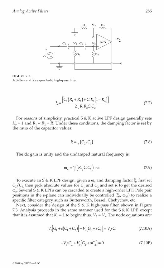
Analog Active Filters 285
(7.7)
For reasons of simplicity, practical S & K active LPF design generally setsKv = 1 and R1 + R2 = R. Under these conditions, the damping factor is set bythe ratio of the capacitor values:
(7.8)
The dc gain is unity and the undamped natural frequency is:
(7.9)
To execute an S & K LPF design, given a wn and damping factor x, first setC2/C1, then pick absolute values for C1 and C2 and set R to get the desiredwn. Several S & K LPFs can be cascaded to create a high-order LPF. Pole pairpositions in the s-plane can individually be controlled (xk, wnk) to realize aspecific filter category such as Butterworth, Bessel, Chebychev, etc.
Next, consider the design of the S & K high-pass filter, shown in Figure7.3. Analysis proceeds in the same manner used for the S & K LPF, exceptthat it is assumed that Kv = 1 to begin; thus, V2 = Vo. The node equations are:
(7.10A)
(7.10B)
FIGURE 7.3A Sallen and Key quadratic high-pass filter.
Vo
+
V1C1 C2
G2G1
V3R RF
Vs
V2IOA
x =+( ) + -( )[ ]C R R C R K
R R C Cv2 1 2 1 1
1 2 1 2
1
2
x = ( )C C2 1
wn R C C= ( )1 1 2 r s
V G s C C V G sC V sCo s1 1 1 2 1 2 1+ +( )[ ] - +[ ] =
- + +[ ] =V sC V G sCo1 2 2 2 0
© 2004 by CRC Press LLC

286 Analysis and Application of Analog Electronic Circuits
Thus,
(7.11)
and:
DVo = Vs s2 C1C2 (7.12)
The S & K HPF transfer function is thus:
(7.13)
When top and bottom are multiplied by R1R2,
(7.14)
Now if C1 = C2 = C, the final form of the HPF transfer function is obtained:
(7.15)
where wnh = 1/[C ] r/s, and xh = .An S & K LPF put in series with an S & K HPF yields a fourth-order band-
pass filter with two low-frequency C-C poles at wnh, a mid-band gain of 1,and a pair of C-C poles from the LPF at wnlo. Clearly, wnh < wnlo. (The BPF isfourth order because it has four poles.) The damping factors, xh and xlo,determine the amount of ringing or transient settling time when the BPF ispresented with a transient input such as an ECG QRS spike. x is usually setbetween 0.707 and 0.5.
The filter’s transfer function is found by first writing the node equations onthe V1 and V2 = Vo nodes:
(7.16A)
(7.16B)
D = + + + + + - -
= + +[ ] + [ ]G G sC C sC G sC G s C C s C sC G s C
G G s C G C G s C C
1 2 2 1 1 2 2 22
1 22
22
2 12
22
1 2 1 2 2 22
1 2
VV
ss C C
s C C s C G C G G Go
s
( ) = [ ] + +[ ] +
21 2
21 2 1 2 2 2 1 2
VV
ss C C R R
s C C R R sR C Co
s
( ) =+ +[ ] +
21 2 1 2
22 1 1 2 1 1 2 1
VV
ss C R R
s C R R sR Co
s
( ) =+ +
2 21 2
2 21 2 12 1
R1R2 R1R2
V G G sC V G sC V Go s1 1 3 1 3 1 1+ +[ ] - +[ ] =
- + + +( )[ ] =V sC V G s C Co1 1 2 1 2 0
© 2004 by CRC Press LLC
A final S & K filter to consider is the quadratic BPF shown in Figure 7.4.

Analog Active Filters 287
The determinant is:
(7.17)
and Vo is found from:
DVo = Vs s C1G1 (7.18)
The BP transfer function is written first as:
(7.19)
To simplify, let C1 = C2 = C and multiply top and bottom by R1 R2 R3:
(7.20)
Next, to put the transfer function in time-constant form, divide top andbottom by (R3 + R1):
(7.21)
The filter’s wn = 1/[C ] r/s; its peak gain at w = wn isR3/(2 R3 + R1) and the BPF’s Q is:
FIGURE 7.4A Sallen and Key quadratic band-pass filter.
Vo
+
C2
G1 V1
G2Vs
C1
G3
V2IOA
D = + + + + + +
+ + - -
= +( ) + +( ) + +( )[ ] +
G G sC G sC G G G sC G sC G sC G
s C s C C sC G s C
G G G s C G G C G G s C C
1 2 1 1 2 1 3 2 1 3 2 3 1 2
212 2
1 2 1 32
12
2 1 3 1 1 2 2 1 32
1 2
VV
ssC G
s C C s C G G C G G G G Go
s
( ) =+ +( ) + +( )[ ] + +( )
1 12
1 2 1 1 2 2 1 3 2 1 3
VV
ssC R R
s C R R R sC R R R R Ro
s
( ) =+ +[ ] + +( )
2 32 2
1 2 3 2 3 1 3 12
VV
ssC R R R R
s C R R R R R sCR R R R Ro
s
( ) =+( )
+( ) + +( ) +( )[ ] +2 3 3 1
2 21 2 3 3 1 2 3 1 3 12 1
R1R2R3( ) R3 R1+( )§
© 2004 by CRC Press LLC
288 Analysis and Application of Analog Electronic Circuits
(7.22)
The S & K BPF’s peak gain and Q are independent of C; C can be used toset wn, once the three resistors are chosen to find the desired Q and peakgain. This is not as easy to design as the S & K LPF and HPF filter.
Before closing this section on Sallen and Key controlled (voltage)-sourcequadratic filters, it should be noted that the designer must simulate thefilter’s behavior with an accurate model of the op amp to be used in orderto predict the filter’s behavior at high frequencies (near the op amp’s fT), aswell as how the filter behaves with transient inputs.
7.2.3 Biquad Active Filters
For many filter applications, the biquad architecture offers ease in designwhen two-pole filters are desired; independent setting of wn, x and mid-bandgain, Kvo, are possible with few components (Rs and Cs). There are twobiquad AF architectures: one-loop and two-loop. One cost of the biquad AFsis that they use more than one op amp (three or four) to realize that whichan S & K AF can do with one op amp. The benefit of the biquad architecture
The two-loop biquad’s transfer functions will be analyzed at the V3, V4,and V5 output nodes. The output at the V5 node is low pass; this can beshown by writing the transfer function using Mason’s rule (Northrop, 1990,Appendix A):
(7.23)
This LPF transfer function can be simplified algebraically to time-constantform:
(7.24)
By comparison with the standard quadratic polynomial form,
wn = 1/R3C r/s (wn set by R3 and C) (7.25A)
x = R/2R2 (damping factor set by R2) (7.25B)
Kvo = R2/R1R2 (dc gain set by R1, once R2 is chosen) (7.25C)
QR R R R R
R R R= =
+( )+( )1 2
21 2 3 3 1
2 3 1
x
VV
sR R R R sR C sR C
R R sR C sR CS
5 1 2 3 3
2 3 3
2
1 1
1 1 1 1 1( ) =
-( ) -( ) -( ) -( )- -( ) -( ) -( ) + -( ) -( )[ ]
VV
sR R R
s R C s RR C RS
52
1 22
32 2
3 2 1( ) =
+ [ ] +
© 2004 by CRC Press LLC
is ease in design. Figure 7.5 shows the one- and two-loop configurations.
Analog Active Filters 289
Next, consider the transfer function for V4. Note that the denominator isthe same as for the V5 transfer function:
(7.26)
Multiplying the numerator and denominator of Equation 7.26 by(–1/sR3C)2 yields:
(7.27)
which is a quadratic BPF. The filter parameters are:
FIGURE 7.5(A) The three-op amp, one-loop biquad active filter. (B) The four-op amp, two-loop biquadactive filter.
V2
V2VS
V3
V3
V4
V5
C
CR1
VS
R R
R
R2
R3
R3
A
B
R
R
C
C
R1
R3
R4 R2
IOA IOA IOA
IOA IOA IOA
IOA
V4
R
VV
sR R R R sR C
R R sR C sR CS
4 1 2 3
2 3 3
2
1
1 1 1 1 1( ) =
-( ) -( ) -( )- -( ) -( ) -( ) + -( ) -( )[ ]
VV
ssR R C R R
s R C s RR C RS
42
3 1 22
32 2
3 2 1( ) =
- ( )+ [ ] +
© 2004 by CRC Press LLC
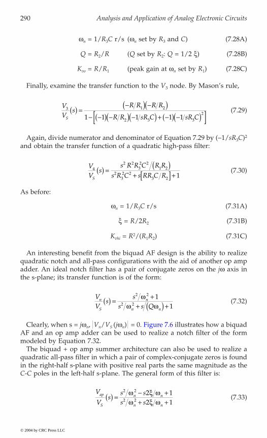
290 Analysis and Application of Analog Electronic Circuits
wn = 1/R3C r/s (wn set by R3 and C) (7.28A)
Q = R2/R (Q set by R2: Q = 1/2 x) (7.28B)
Kvo = R/R1 (peak gain at wn set by R1) (7.28C)
Finally, examine the transfer function to the V3 node. By Mason’s rule,
(7.29)
Again, divide numerator and denominator of Equation 7.29 by (-1/sR3C)2
and obtain the transfer function of a quadratic high-pass filter:
(7.30)
As before:
wn = 1/R3C r/s (7.31A)
x = R/2R2 (7.31B)
Kvhi = R2/(R1R2) (7.31C)
An interesting benefit from the biquad AF design is the ability to realizequadratic notch and all-pass configurations with the aid of another op ampadder. An ideal notch filter has a pair of conjugate zeros on the jw axis inthe s-plane; its transfer function is of the form:
(7.32)
Clearly, when s = jwn, Vn/VS n
AF and an op amp adder can be used to realize a notch filter of the formmodeled by Equation 7.32.
The biquad + op amp summer architecture can also be used to realize aquadratic all-pass filter in which a pair of complex-conjugate zeros is foundin the right-half s-plane with positive real parts the same magnitude as theC-C poles in the left-half s-plane. The general form of this filter is:
(7.33)
VV
sR R R R
R R sR C sR CS
3 1 2
2 3 3
21 1 1 1 1
( ) =-( ) -( )
- -( ) -( ) -( ) + -( ) -( )[ ]
VV
ss R R C R R
s R C s RR C RS
42 2
32 2
1 22
32 2
3 2 1( ) = ( )
+ [ ] +
VV
ss
s s Qn
S
n
n n
( ) =+
+ ( ) +
2 2
2 2
11
ww w
V
Vs
s ss s
ap
S
n n
n n
( ) =- ++ +
2 2
2 2
2 12 1
w x ww x w
© 2004 by CRC Press LLC
(jw ) = 0. Figure 7.6 illustrates how a biquad
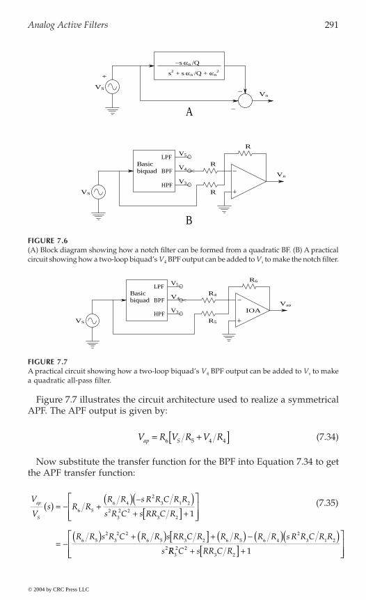
Analog Active Filters 291
Figure 7.7 illustrates the circuit architecture used to realize a symmetricalAPF. The APF output is given by:
(7.34)
Now substitute the transfer function for the BPF into Equation 7.34 to getthe APF transfer function:
FIGURE 7.6(A) Block diagram showing how a notch filter can be formed from a quadratic BF. (B) A practicalcircuit showing how a two-loop biquad’s V4 BPF output can be added to Vs to make the notch filter.
FIGURE 7.7A practical circuit showing how a two-loop biquad’s V4 BPF output can be added to Vs to makea quadratic all-pass filter.
VS
+
−
−s ωn /Q
−
s2 + s ωn /Q + ωn2
Vn
Vn
R
R
R
V3
V4
V5LPF
BPF
HPFVS
Basicbiquad
A
B
V3
LPF
BPF
HPF
biquadR4V4
Basic
IOAVap
R6
VS
V5
R5
V R V R V Rap S= +[ ]6 5 4 4
V
Vs R R
R R s R R C R R
s R C s RR C R
R R s R C R R s RR C R R R R R s R R C R R
s
ap
S
( ) ( )( )[ ]
È
ÎÍÍ
ù
ûúú
( ) ( ) [ ] ( ) ( )( )
= - +-
+ +
= -+ + -
6 5
6 42
3 1 2
232 2
3 2
6 52
32 2
6 5 3 2 6 5 6 42
3 1 2
2
1
RR C s RR C R32 2
3 2 1+ +[ ]È
ÎÍÍ
ù
ûúú
(7.35)
© 2004 by CRC Press LLC

292 Analysis and Application of Analog Electronic Circuits
To obtain the symmetric APF, let R1 = R; R5 = 2R4; and R6 = R5. The desiredtransfer function is then:
(7.36)
The natural frequency of poles and zeros is:
wn = 1/R3C r/s (7.37A)
x = R/2R2 (7.37B)
Kvo = -1, - £ w £ (7.37C)
The purpose of all-pass filters is to generate a phase shift with frequencywith no attenuation; the phase of the APF described earlier can be shown tobe:
(7.38)
7.2.4 Generalized Impedance Converter AFs
Often one wishes to design AFs that work at very low frequencies, e.g., below20 Hz. Such filters can find application in conditioning low-frequency phys-iological signals such as the ECG, EEG, and heart sounds. If a conventionalbiquad AF is used to make a high-pass filter whose fn = 1 Hz, for example,it is necessary to obtain very large capacitors that are expensive and take upexcessive volume on a PC board. For example, the capacitor required for fn =1 Hz and R3 = 100 kW is:
(7.39)
a small capacitor, e.g., 0.001 mF, to be magnified electronically, transformedinto a large, equivalent, very high-Q inductor, or made into a D-element thatcan be shown to have the impedance, ZD(w) = 1/(w2 D), where D is deter-mined by certain Rs and Cs as shown next.
Find an expression for the driving point impedance of the general GICcircuit, Z11 = V1/I1. Clearly, from Ohm’s law:
(7.40)
V
Vs
s R C sR CR Rs R C sR CR R
ap
S
( ) = -- ++ +
232 2
3 22
32 2
3 2
11
j pw
w= - -
-È
ÎÍ
ù
ûú-2
1 21 3 2
23
3tanR CR R
R C radians
Cf Rn
= =12
1 593p
m. F
Z V IV
V V Z11 1 11
1 2 1
= =-( )
© 2004 by CRC Press LLC
The GIC circuit, shown in general format in Figure 7.8, allows the size of
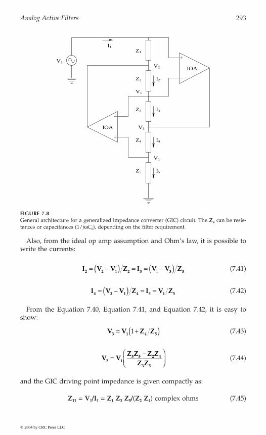
Analog Active Filters 293
Also, from the ideal op amp assumption and Ohm’s law, it is possible towrite the currents:
(7.41)
(7.42)
From the Equation 7.40, Equation 7.41, and Equation 7.42, it is easy toshow:
(7.43)
(7.44)
and the GIC driving point impedance is given compactly as:
Z11 = V1/I1 = Z1 Z3 Z5/(Z2 Z4) complex ohms (7.45)
FIGURE 7.8General architecture for a generalized impedance converter (GIC) circuit. The Zk can be resis-tances or capacitances (1/jwCk), depending on the filter requirement.
IOA
I2
I3
Z1
I1
Z2
Z3
Z4
Z5
V1V2
IOA V3
I5
V1
I4
V1
I V V Z I V V Z2 2 1 2 3 3 3= -( ) = = -( )1
I V V Z I V Z4 3 1 4 5 1 5= -( ) = =
V V Z Z3 1 4 5= +( )1
V VZ Z Z Z
Z Z2 13 5 2 4
3 5
=-Ê
ËÁ
© 2004 by CRC Press LLC
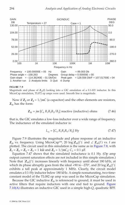
294 Analysis and Application of Analog Electronic Circuits
Now if Z2 or Z4 = 1/jwC (a capacitor) and the other elements are resistors,Z11 has the form:
Z11 = jw [C4 R1R3R5/R2] reactive (inductive) ohms (7.46)
that is, the GIC emulates a low-loss inductor over a wide range of frequency.The inductance of the emulated inductor is:
Leq = [C4 R1R3R5/R2] Hy (7.47)
Figure 7.9 illustrates the magnitude and phase response of an inductiveZ11 vs. frequency. Using MicroCap, 20 log Z11(f ) and Z11(f ) vs. f are
Z1 = Z3 = Z4 = Z5 = 1 kW and Z2 = 1/jwC2; C2 = 0.1 mF.Equation 7.47 shows that the simulated inductance is 0.1 Hy. (Op amp
output current saturation effects are not included in this simple simulation.)Note that Z11(f ) increases linearly with frequency until about 180 kHz, atwhich its phase abruptly goes from the ideal +90 to –270∞, and 20 log Z11(f ) exhibits a tall peak at approximately 1 MHz. Clearly, the circuit modelemulates a 0.1-Hy inductor below 180 kHz. A simple nonsaturating, two-time-constant model of the TL082 op amp was used in the MicroCap simulation.
Because the GIC inductive Z11 is referenced to ground, it must be used in
FIGURE 7.9Magnitude and phase of Z11(f) looking into a GIC emulation of a 0.1-HY inductor. In thisMicroCap simulation, TL072 op amps were used. Smooth line is magnitude.
© 2004 by CRC Press LLC
plotted. The circuit used in this simulation is the same as in Figure 7.8, with
active filters that require inductors with one end tied to ground. Figure7.10(A) illustrates an inductive GIC used in a simple high-Q, quadratic BPF.
Frequency = 100.00000E + 05 Hz Gain = 89.003 DbPhase angle = −158.263 Degrees Group delay = 0.00000E + 00Gain slope = −114.36240E − 01 Db/Oct Peak gain = 128.556 Db/F = 107.01700E + 041: Another run 2: Analysis limits 3: Quit 4: Dump
Frequency in Hz
Case = 1
GICINDUC
Temperature = 27
GAINDB
130.00
104.00
78.00
52.00
26.00
0.00100 1K 100K 1M 10M10K
PHASEDEG
−360.0
−270.0
−180.0
−90.0
0.0
90.0

Analog Active Filters 295
Figure 7.10(B) illustrates a simple R–L–C BPF suitable for circuit analysis. Anode equation gives the BPF’s transfer function:
(7.48)
In this filter:
(7.49A)
(7.49B)
(7.49C)
Leq is given by Equation 7.47.
FIGURE 7.10(A) Circuit of an RLC band-pass filter using the GIC inductor. The GIC circuit allows emulationof a very large, high-Q inductor over a wide range of frequencies and is particularly well suitedfor making filters in the subaudio range of frequencies. (B) The actual BPF.
IOA
VS C
I1Z11
Leq
C
I1
V1 = Vo
R V1
Vo
Vo
+
+
+
−
−
R
+
VS
GICINDUCTOR
A
B
VV
ssL R
s C L sL Ro
S
eq
eq eq
( ) =+ +2 1
wn eqCL= 1 r s
Q R C Leq= ( ) =1 2x
VV
o
S
j nw( ) = ∞1 0
© 2004 by CRC Press LLC
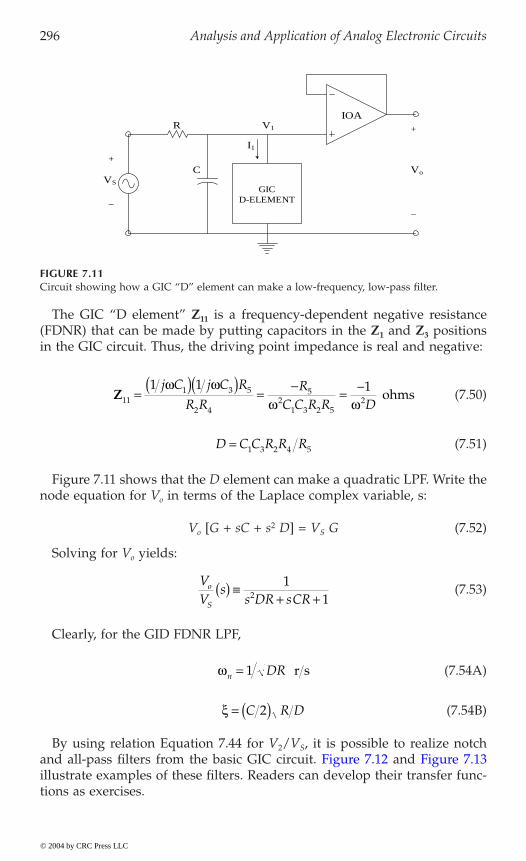
296 Analysis and Application of Analog Electronic Circuits
The GIC “D element” Z11 is a frequency-dependent negative resistance(FDNR) that can be made by putting capacitors in the Z1 and Z3 positionsin the GIC circuit. Thus, the driving point impedance is real and negative:
(7.50)
(7.51)
Figure 7.11 shows that the D element can make a quadratic LPF. Write thenode equation for Vo in terms of the Laplace complex variable, s:
Vo [G + sC + s2 D] = VS G (7.52)
Solving for Vo yields:
(7.53)
Clearly, for the GID FDNR LPF,
(7.54A)
(7.54B)
By using relation Equation 7.44 for V2/VS, it is possible to realize notch
illustrate examples of these filters. Readers can develop their transfer func-tions as exercises.
FIGURE 7.11Circuit showing how a GIC “D” element can make a low-frequency, low-pass filter.
I1
V1R
GICD-ELEMENT
VS
−
+
IOA+
C o
−
V
Z111 3 5
2 4
52
1 3 2 52
1 1 1= ( )( ) =-
= -j C j C R
R RR
C C R R D
w ww w
ohms
D C C R R R= 1 3 2 4 5
VV
ss DR sCR
o
S
( ) ∫+ +
112
wn DR= 1 r s
x = ( )C R D2
© 2004 by CRC Press LLC
and all-pass filters from the basic GIC circuit. Figure 7.12 and Figure 7.13
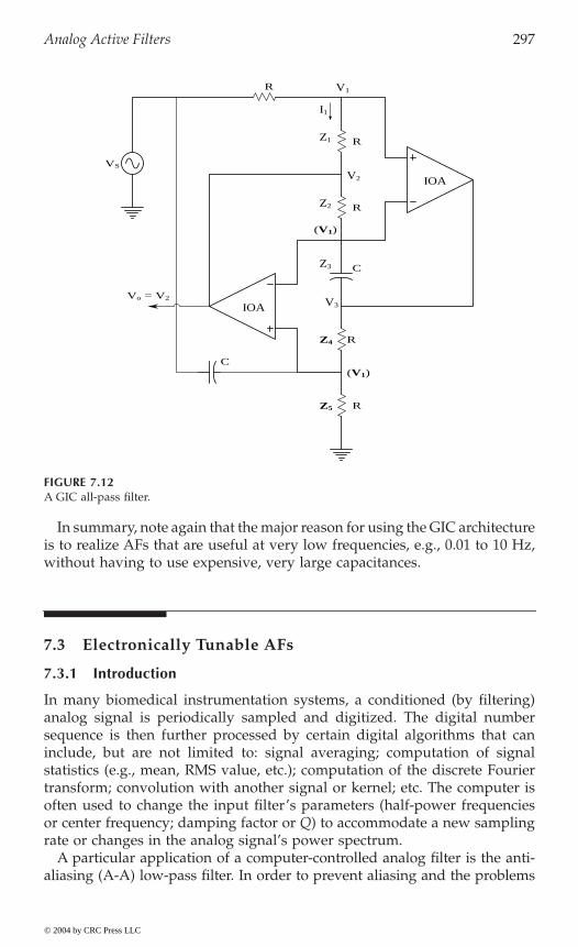
Analog Active Filters 297
In summary, note again that the major reason for using the GIC architectureis to realize AFs that are useful at very low frequencies, e.g., 0.01 to 10 Hz,without having to use expensive, very large capacitances.
7.3 Electronically Tunable AFs
7.3.1 Introduction
In many biomedical instrumentation systems, a conditioned (by filtering)analog signal is periodically sampled and digitized. The digital numbersequence is then further processed by certain digital algorithms that caninclude, but are not limited to: signal averaging; computation of signalstatistics (e.g., mean, RMS value, etc.); computation of the discrete Fouriertransform; convolution with another signal or kernel; etc. The computer isoften used to change the input filter’s parameters (half-power frequenciesor center frequency; damping factor or Q) to accommodate a new samplingrate or changes in the analog signal’s power spectrum.
A particular application of a computer-controlled analog filter is the anti-aliasing (A-A) low-pass filter. In order to prevent aliasing and the problems
FIGURE 7.12A GIC all-pass filter.
VS
R V1
I1
RZ1
C
R
(V1)
R
RZ2
C
(V1)
V3
V2 IOA
IOA
Z3
Z5
Z4
Vo = V2
© 2004 by CRC Press LLC

298 Analysis and Application of Analog Electronic Circuits
this creates for the signal in digital form, the A-A filter must pass no significantsignal spectral power to the analog-to-digital converter at frequencies aboveone half the sampling frequency, fs. fs/2 is called the Nyquist frequency, fn. (See
The key to designing a digitally tuned filter is the variable gain element(VGE) (Northrop, 1990, Section 10.1). The design of digitally-controlled vari-able gain elements (DCVGEs) has several approaches: one uses a digital-to-analog converter (DAC) configured to produce 0 to 10 Vdc output, VC, whichis the input to an analog multiplier IC; the other input to the analog multiplieris the time-variable analog signal, vk (t), whose amplitude is to be adjusted.The output of the analog multiplier is then vk¢(t) = vk (t)VC/10. VC/10 variesfrom 0 to 1 in steps determined by the quantization set by the number ofbinary bits input to the DAC. Another VGE is the digitally programmed gainamplifier (DPGA), with a gain digitally selected in 6-dB steps (i.e., 1, 2, 4, 8,16, 32, 64, and 128) using a 3-bit input word (e.g., the MN2020). Still anotherclass of DCVGE is represented by the AD8400, 8-bit, digitally controlled poten-tiometer (DCP) connected as a variable resistor. The DCP resistance is given by:
(7.55)
FIGURE 7.13A GIC notch filter.
VS
R V1
I1
RZ1
C
R
(V1)
R
RZ2
C
(V1)
V3
V2 IOA
IOA
Z3
Z5
Z4
R
Vo = V2
¢ = =- +( )
=ÂV R B R Aj total k
k N
k
N
total k2 1
1
© 2004 by CRC Press LLC
Section 10.2 in Chapter 10 for a complete treatment of sampling and aliasing.)
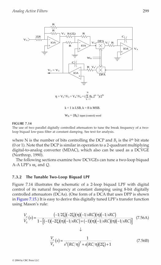
Analog Active Filters 299
where N is the number of bits controlling the DCP and Bk is the kth bit state(0 or 1). Note that the DCP is similar in operation to a 2-quadrant multiplyingdigital-to-analog converter (MDAC), which also can be used as a DCVGE(Northrop, 1990).
The following sections examine how DCVGEs can tune a two-loop biquadA-A LPF’s wn and Q.
7.3.2 The Tunable Two-Loop Biquad LPF
Figure 7.14 illustrates the schematic of a 2-loop biquad LPF with digitalcontrol of its natural frequency at constant damping using 8-bit digitallycontrolled attenuators (DCAs). (One form of a DCA that uses DPP is shown
using Mason’s rule:
(7.56A)
Ø
(7.56B)
FIGURE 7.14The use of two parallel digitally controlled attenuators to tune the break frequency of a two-loop biquad low-pass filter at constant damping. See text for analysis.
IOAIOA
IOA
WN
VS
V2
V3 V3’
V4
V4’V5 = Vo
C
C
R
R
R
R
R
R
R/(2x)2xR
DPA
IOADPA
N
h = V3’/V3 = V4’/V4 = ( S Bk 2k -1)/2N
k = 1
k = 1 is LSB, k = 8 is MSB.
WN = Bk input (control) word
VV
ssRC sRC
sRC sRC sRCo
S
( ) =-( ) -( )( ) -( )( ) -( )
- -( ) -( )( ) -( ) + -( )( ) -( )( ) -( )[ ]1 2 2 1 1
1 1 2 1 1 1 1
x x h hx h h h
VV
ss RC s RC
o
S
( ) =( ) + ( )( ) +
1
2 12 2h h x
© 2004 by CRC Press LLC
in Figure 7.15.) It is easy to derive this digitally tuned LPF’s transfer function

300 Analysis and Application of Analog Electronic Circuits
From the standard quadratic format:
wn = h/RC r/s (7.57)
The constant damping, x, is set by the size of the input resistor (2 xR) andthe resistor size V2 sees (R/2 x). Thus, with 1 LSB in, Wn = 0,0,0,0,0,0,0,1,wn = (1/256)(1/RC) r/s; with WN = 1,1,1,1,1,1,1,1, wn = (255/256)(1/RC)r/s. The dc gain of the filter is +1.
As a second example, consider the digitally controlled band-pass filterN1 and WN2)
are used to set the filter’s natural frequency, wn, and a third variable gainelement is used to adjust the filter’s Q. In this example, digitally controlledamplifier gains are used. Using Mason’s rule as before, the transfer functioncan be written as:
(7.58)
Ø
(7.59)
where the resonant frequency is set by A2 and the Q by 1/A1:
wn = A2/RC r/s (7.60A)
Q = 128/A1 (7.60B)
FIGURE 7.15Schematic of a digitally controlled attenuator (DCA).
Vo = ηVin
IOA
Vin
DCP
WN
η Rtotal
(1 − η) Rtotal
BufferηVin
A DCA
VV
ssRC
sRC sRC sRCS
41 1 128 1
1 1 1 128 1 1 1 1( ) =
-( ) -( ) -( )- -( ) -( ) -( ) + -( ) -( ) -( )[ ]
A A
A A A A1 2
1 2 2 2
VV
ss RC
s RC sRCS
42 2
128
128 1( ) =
- ( )( ) + ( ) +
A A
A A A1 2
2 1 2
© 2004 by CRC Press LLC
shown in Figure 7.16 in which two N-bit, serial binary words (W
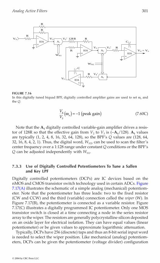
Analog Active Filters 301
(7.60C)
Note that the A1 digitally controlled variable-gain amplifier drives a resis-tor of 128R so that the effective gain from V2 to V3 is (-A1/128). A1 valuesare typically (1, 2, 4, 8, 16, 32, 64, 128), so the BPF’s Q values are (128, 64,32, 16, 8, 4, 2, 1). Thus, the digital word, WN2, can be used to scan the filter’scenter frequency over a 1:128 range under constant Q conditions or the BPF’sQ can be adjusted independently with WN1.
7.3.3 Use of Digitally Controlled Potentiometers To Tune a Sallen and Key LPF
Digitally controlled potentiometers (DCPs) are IC devices based on the
eter. Note that the potentiometer has three leads: two to the fixed resistor(CW and CCW) and the third (variable) connection called the wiper (W). InFigure 7.17(B), the potentiometer is connected as a variable resistor. Figure7.17(C) illustrates a digitally programmed IC potentiometer. Only one MOStransistor switch is closed at a time connecting a node in the series resistorarray to the wiper. The resistors are generally polycrystalline silicon depositedon an oxide layer for electrical isolation. They can have equal values (linearpotentiometer) or be given values to approximate logarithmic attenuation.
Typically, DCPs have 256 (discrete) taps and thus an 8-bit serial input wordis needed to select the wiper position. Like mechanical (analog) potentiom-eters, DCPs can be given the potentiometer (voltage divider) configuration
FIGURE 7.16In this digitally tuned biquad BPF, digitally controlled amplifier gains are used to set wn andthe Q.
R
R V4’
C
V3’V3 R
V5
WN1
WN2
A1
A2
R
R
R
C
IOA
IOAIOA
IOA
VS V2 V2’ 128 R
R A2 V4 = Vo
VVS
n4 1w( ) = - ( ) peak gain
© 2004 by CRC Press LLC
nMOS and CMOS transistor switch technology used in certain ADCs. Figure7.17(A) illustrates the schematic of a simple analog (mechanical) potentiom-
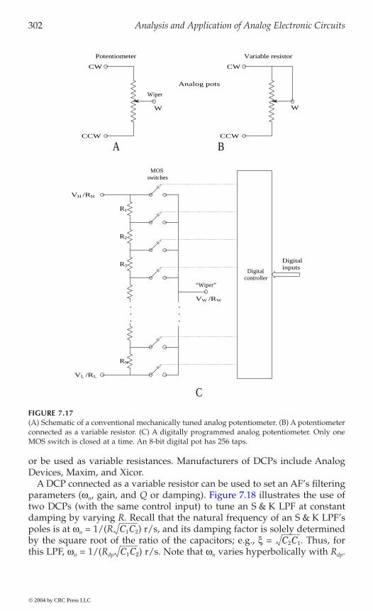
302 Analysis and Application of Analog Electronic Circuits
or be used as variable resistances. Manufacturers of DCPs include AnalogDevices, Maxim, and Xicor.
A DCP connected as a variable resistor can be used to set an AF’s filteringn
two DCPs (with the same control input) to tune an S & K LPF at constantdamping by varying R. Recall that the natural frequency of an S & K LPF’spoles is at wn = 1/(R ) r/s, and its damping factor is solely determinedby the square root of the ratio of the capacitors; e.g., x = . Thus, forthis LPF, wn = 1/(Rdp ) r/s. Note that wn varies hyperbolically with Rdp.
FIGURE 7.17(A) Schematic of a conventional mechanically tuned analog potentiometer. (B) A potentiometerconnected as a variable resistor. (C) A digitally programmed analog potentiometer. Only oneMOS switch is closed at a time. An 8-bit digital pot has 256 taps.
.
.
.
.
.
.
MOSswitches
Digitalcontroller
R1
R2
R3
RN
“Wiper”
Variable resistor
A B
C
CW CW
Potentiometer
CCW CCW
W
Wiper
Analog pots
VH /RH
VL /RL
VW /RW
Digitalinputs
W
C1C2
C2C1
C1C2
© 2004 by CRC Press LLC
parameters (w , gain, and Q or damping). Figure 7.18 illustrates the use of
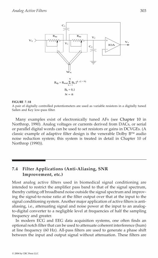
Analog Active Filters 303
Northrop, 1990). Analog voltages or currents derived from DACs, or serialor parallel digital words can be used to set resistors or gains in DCVGEs. (Aclassic example of adaptive filter design is the venerable Dolby B audionoise reduction system; this system is treated in detail in Chapter 10 ofNorthrop (1990)).
7.4 Filter Applications (Anti-Aliasing, SNR Improvement, etc.)
Most analog active filters used in biomedical signal conditioning areintended to restrict the amplifier pass band to that of the signal spectrum,thereby cutting off broadband noise outside the signal spectrum and improv-ing the signal-to-noise ratio at the filter output over that at the input to thesignal conditioning system. Another major application of active filters is anti-aliasing, i.e., attenuating signal and noise power at the input to an analog-to-digital converter to a negligible level at frequencies of half the samplingfrequency and greater.
In modern ECG and EEG data acquisition systems, one often finds anoptional notch filter that can be used to attenuate coherent interference (hum)at line frequency (60 Hz). All-pass filters are used to generate a phase shiftbetween the input and output signal without attenuation. These filters are
FIGURE 7.18A pair of digitally controlled potentiometers are used as variable resistors in a digitally tunedSallen and Key low-pass filter.
Rdp Rdp
C2
C1
V1 IOAVo
V2
VS
WN
N
Rdp = Rtotal S Bk 2k -(1 + N)
k = 1
Bk = 0,1
N = 8
© 2004 by CRC Press LLC
Many examples exist of electronically tuned AFs (see Chapter 10 in
304 Analysis and Application of Analog Electronic Circuits
used to adjust synchronization signal phase in lock-in amplifiers and syn-chronous rectifiers, and to correct for phase lags inherent in data transmis-sion on coaxial cables and other transmission lines.
7.5 Chapter Summary
7.5.1 Active Filters
There are many op amp active filter architectures. Some are easier to use indesigning than others. This chapter focused on the easy ones: the controlled-source Sallen and Key filters; the biquad active filter family; and filters basedon the generalized impedance converter circuit (GIC). Also covered were thedesign and analysis of electronically tunable active filters using variable-gainelements such as analog multipliers, multiplying DACs, digitally controlledpotentiometers, and digitally controlled gain amplifiers. Electronically tunedfilters have application as anti-aliasing filters and tuned filters that can tracka coherent signal’s frequency — to compensate for Doppler shift, for example.
Although not covered in this chapter, a family of active filters calledswitched-capacitor filters (SCFs) are primarily used in telecommunications. TheSCFs use MOS switches to commute capacitors in what would otherwise bean op amp, R–C filter design. The switched capacitor can be shown toemulate a resistor of value Req = Tc/Cs, where Tc is the period of the commu-tation and Cs is the switched capacitor value. The interested reader canconsult Section 9.2 in Northrop (1990).
7.5.2 Choice of AF Components
Because most analog AFs used in biomedical applications operate on signalsin the 0- to 5-kHz range, overall filter high-frequency response is often notan important consideration. Instead, concern is with noise, linearity, dc drift,and stability of parameter settings (dc gain, wn, and damping, x). To minimizenoise and maximize parameter stability, metal film resistors (or wire-woundresistors) with low tempcos are generally chosen.
Choice of capacitors is important in determining filter linearity. Some capac-itor dielectrics exhibit excessive losses, unidirectional dc leakage, and dielectrichysteresis; thus they can distort filtered signals. In particular, electrolytic andtantalum dielectric capacitors are not recommended for AF components; theyare usually used for bypassing applications where they are operated with afixed dc voltage bias. Polycarbonate dielectric capacitors can also distortsignals. The best capacitor dielectrics are air, mica, ceramic, oiled paper, andmylar. Again, low tempcos are desired. Do not be tempted to use electrolyticor tantalum capacitors in an AF design that requires large capacitor valuesin order to realize a low wn. Instead, use a GIC design for the filter that usessmaller Cs.
© 2004 by CRC Press LLC
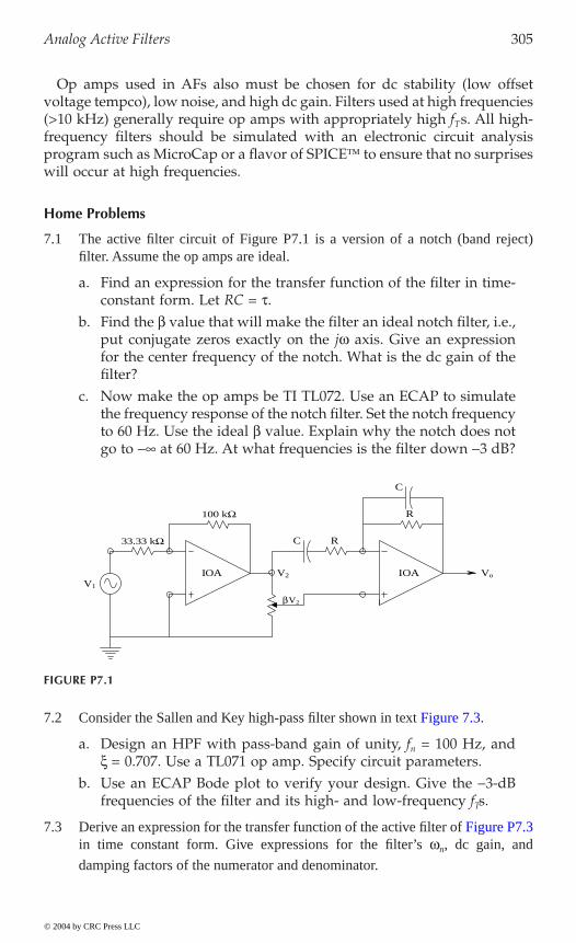
Analog Active Filters 305
Op amps used in AFs also must be chosen for dc stability (low offsetvoltage tempco), low noise, and high dc gain. Filters used at high frequencies(>10 kHz) generally require op amps with appropriately high fTs. All high-frequency filters should be simulated with an electronic circuit analysisprogram such as MicroCap or a flavor of SPICE to ensure that no surpriseswill occur at high frequencies.
Home Problems
7.1 The active filter circuit of Figure P7.1 is a version of a notch (band reject)filter. Assume the op amps are ideal.
a. Find an expression for the transfer function of the filter in time-constant form. Let RC = t.
b. Find the b value that will make the filter an ideal notch filter, i.e.,put conjugate zeros exactly on the jw axis. Give an expressionfor the center frequency of the notch. What is the dc gain of thefilter?
c. Now make the op amps be TI TL072. Use an ECAP to simulatethe frequency response of the notch filter. Set the notch frequencyto 60 Hz. Use the ideal b value. Explain why the notch does notgo to - at 60 Hz. At what frequencies is the filter down -3 dB?
7.2
a. Design an HPF with pass-band gain of unity, fn = 100 Hz, andx = 0.707. Use a TL071 op amp. Specify circuit parameters.
b. Use an ECAP Bode plot to verify your design. Give the -3-dBfrequencies of the filter and its high- and low-frequency fTs.
7.3in time constant form. Give expressions for the filter’s wn, dc gain, and
damping factors of the numerator and denominator.
FIGURE P7.1
33.33 kΩ
βV2
V2
C R
V1
Vo
R
C
100 kΩ
IOA IOA
© 2004 by CRC Press LLC
Consider the Sallen and Key high-pass filter shown in text Figure 7.3.
Derive an expression for the transfer function of the active filter of Figure P7.3

306 Analysis and Application of Analog Electronic Circuits
7.4 Design a band-pass filter for neural spike signal conditioning using twocascaded quadratic Sallen and Key active filters (1 LP, 1 HiP) with thefollowing specifications: mid-band gain = 0 dB; -3 dB fLO = 300 Hz; xLO =0.5; -3 dB fHI = 4 kHz; and xHI = 0.5. (Note that the filter -3dB-frequenciesare not necessarily their fns.) Use OP-27 op amps. Specify the R and C values.Note: all Rs must be between 103 and 106 W and C values must lie between3 pF and 3 mF. Verify your design with a PSpice or MicroCap Bode plot.
7.5 Design a quadratic GIC band-pass filter for geophysical applications tocondition a seismometer output having fn = 1 Hz and Q = 10. Verify yourdesign with a Bode plot done with MicroCap or PSpice. Use the same rangesof Rs and Cs as in the preceding problem.
7.6
a. Write the transfer function, V4/V1 in time-constant form.b. Write the transfer function, V2/V1, for the AF in TC form. Give
expressions for wn, Q, and V2/V1 at wn.c. Write an expression for the transfer function, V5/V1, in time
constant form. Use an ECAP to make a Bode plot of V5/V1. LetR = 1 kW; R1 = 10 kW; R4 = 1 kW; and C = 10 nF. Op amps areTL074s.
7.7 Find an expression for V4/V1 in time-constant form for the biquad AF shown in
n 4 1 n
7.8used as the variable-gain element (VGE). The analog multiplier output V3 =–V2Vc./10.
a. Derive an expression for Vo/V1 in time-constant form.b. Make a dimensioned Bode plot of Vo/V1. Give expressions for
the dc gain and the break frequency.
FIGURE P7.3
R
R
4RC
C
R Vi
Vi’
V1
Vo
© 2004 by CRC Press LLC
For the three-op amp biquad AF shown in Figure P7.6
Figure P7.7. Give expressions for w , Q and V /V at w . Assume ideal op amps.
Figure P7.8 illustrates a voltage-tunable, 1-pole LPF. An analog multiplier is
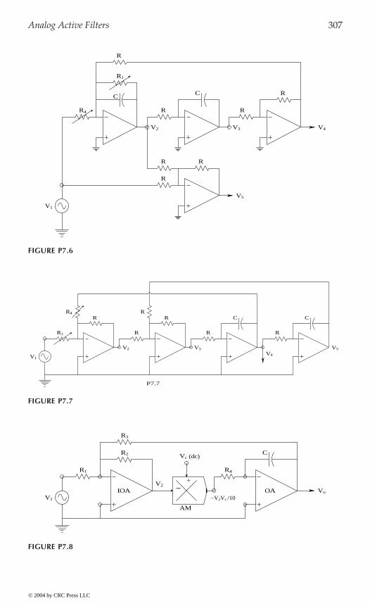
Analog Active Filters 307
FIGURE P7.6
FIGURE P7.7
FIGURE P7.8
R
R R
R
RR
R
R4
R1
CC
V1
V2 V3 V4
V5
CCRR
R
R
R RR1
R4
V5
V4
V3V2
V1
P7.7
Vc (dc)
Vo
AM
R1
R2
R3
C
R4
+
−IOA I OAV2
V1 −V2Vc /10
© 2004 by CRC Press LLC
308 Analysis and Application of Analog Electronic Circuits
7.9 Figure P7.9 illustrates another voltage-tuned active filter.
a. Derive an expression for Vo/V1 in time-constant form.b. Make a dimensioned Bode plot of Vo/V1. Give expressions for
the dc gain and the break frequency.
7.10 The circuit of Figure P7.10 is an op amp AF realization of a Dolby B audionoise reduction system recording encoder. It is designed to boost the high-frequency response of magnetic tape-recorded signals containing little powerat high frequencies in order to improve playback signal-to-noise ratio (whenused in conjunction with a Dolby B™ decoder filter). (Magnetic tape has anomnipresent high-frequency background “hiss” on playback, regardless ofsignal strength.)
a. Derive an expression for Vo/V1 in time-constant form.b. Make a dimensioned Bode plot of Vo/V1. Give expressions for
the dc gain and the break frequencies.
FIGURE P7.9
FIGURE P7.10
Vc (dc)
Vo
AM
V1
R1
R2 C
R4
+
−
IOA I OA V2
R3 −V2Vc /10
C1 C2
R
R
R
R
R
R/10
Vc > 0
V1
Vo
V2
V3 +−IOA I OAIOA
AM
V4
© 2004 by CRC Press LLC
Analog Active Filters 309
7.11 The circuit of Figure P7.11 is an op amp AF realization of a Dolby B audionoise reduction system decoder. It is designed to attenuate the high-frequencyresponse of recorded signals containing high frequencies in order to improveplayback signal-to-noise ratio (when used in conjunction with a Dolby Bencoder filter).
a. Derive an expression for Vo/V1 in time-constant form.b. Make a dimensioned Bode plot of Vo/V1. Give expressions for
the dc gain and the break frequencies.
7.12MDACs are used as variable gain elements (VGEs). The analog input signal tothe MDAC is multiplied by a fraction determined by the digital word input tothe MDAC. For example, for MDAC1, its output is the analog signal:
where N is the number of binary bits in the word, D1k = 0,1; for N = 8, themaximum gain is 255/256 (All D1k = 1) and the minimum gain is 0/256 (allD1k = 0).
a. Find the transfer function, (Vo/V1)(s) in Laplace format.b. Give expressions for the filter’s wn, Q, and peak gain in terms of
D1k, D2k, and system parameters. What is the range of Q?Assume N = 8 bits and the op amps are ideal.
FIGURE P7.11
C1
C2R
R
RR1 Vc > 0
V1
Vo
V2 +−IOA I OA
AM
V3
V VD k
kN
N3 2
112
2=
-Â
© 2004 by CRC Press LLC
The circuit of Figure P7.12 is a digitally tunable biquad band-pass filter.

310 Analysis and Application of Analog Electronic Circuits
7.13 Derive the transfer function in time-constant form for the GIC all-pass filter of
7.14 Derive the transfer function in time-constant form for the GIC notch filter of
FIGURE P7.12
RR
R
R
R
R R
MDAC2
MDAC3
MDAC1
C
R
V1
V2
V3
V4
V5
Vo
V7
V8
CD2D1
© 2004 by CRC Press LLC
Figure 7.12 in the text.
Figure 7.13 in the text.
311
8Instrumentation and Medical Isolation Amplifiers
8.1 Introduction
Instrumentation amplifiers (IAs) are basically differential amplifiers charac-terized by very high input impedance, very high common-mode rejectionratio (CMRR), and differential gain set by a single resistor, generally in therange from ¥1 to ¥1000. In addition, IAs also have low noise, offset voltage,bias current, and offset current.
Medical isolation amplifiers (IsoAs) provide an ultra-low conductive path-way between the input (patient) terminals and the output terminals andground. This pathway provides what is called ohmic or galvanic isolationfor a patient. In medical applications, this isolation is required for reasonsof patient safety. The dc resistance between input and output terminals istypically on the order of gigaohms (thousands of megohms); at ac, capaci-tance between input and output terminals is on the order of single picofarad.There are five established isolation architectures
1. Transformer isolation in which power is coupled to the (isolated)input stage by high-frequency current and signal is coupled to theoutput stage also by transformer, by modulating the power supplyoscillator frequency
2. Photo-optic coupling in which the isolated conditioned input signalis coupled to the output by means of photo-optic couplers (using anLED and a photodiode or photoresistor). Power is still suppliedthrough high-frequency isolation transformer.
3. Capacitive coupling of a signal-modulated, high-frequency digitalcarrier from the isolated input stage through a pair of 1-pF capacitorsto a demodulator in the output stage
4. Magnetic coupling using giant magnetoresistive resistors (GMRs) ina Wheatstone bridge. A GMR’s resistance is altered by its localmagnetic field. The isolated input signal is converted to a current
© 2004 by CRC Press LLC
312 Analysis and Application of Analog Electronic Circuits
that is passed through coils in close proximity to two GMRs in abridge. The DRs unbalance the bridge, which is on the output sideof the IA. The unbalance is detected by a DA, which generates acurrent used to re-null the bridge. The renulling current is sensedand is proportional to the input voltage. Isolation is maintained bythe ohmic isolation between the input coils and the GMR bridgeresistors.
5. The flying capacitor chopper circuit uses a small capacitor chargedup by the signal voltage and then switched by a high-speed DPDTrelay to an output amplifier that reads the voltage across the capac-itor. Such switched-capacitor IAs have ohmic isolation set by therelay structure and are useful only for dc or very low-frequencysignals.
8.2 Instrumentation Amps
IAs, per se, are not suitable for medical applications because medical ampli-fiers require severe ohmic (galvanic) isolation. Medical amplifiers can useIAs in their front ends, however. Several IC manufacturers make IAs, e.g.,Burr–Brown and Analog Devices.
This section first examines some of the properties of a low-cost, low-powerIA, the AD620. This device can have its differential gain set from 1 to 103 bya single resistor. The -3-dB bandwidth (BW) varies with gain in accordancewith the gain ¥ bandwidth constancy relation. At Av = 103, the BW is approx-imately 10 kHz; at Av = 100, the BW is approximately 120 kHz; at Av = 10,the BW is approximately 400 kHz; and at Av = 1, the BW is approximately1 MHz.
The equivalent short-circuit input voltage noise root power spectrumdepends on Av. For Av = 100, 103, ena = 9 nV/÷Hz at 1 kHz. The input noiseincreases as the gain Av decreases. Input current noise ina = 100 fA RMS/÷Hz,regardless of gain. The AD620’s CMRR varies with gain, ranging from 90 dBat Av = 1 to 130 dB at Av = 103. This IA’s input bias current, IB, = 0.5 nA; theinput offset voltage, Vos, is 15 mV. The input impedance is 10 GWúÁ2 pF for
A low-noise precision IA, the AMP01 by Analog Devices, offers slightlydifferent specifications. The gain is set between 1 and 103 by a single resistor.The -3-dB bandwidths are approximately 26, 82, 100, and 570 kHz for gainsof 103, 102, 10, and 1, respectively. The short-circuit input voltage noise rootspectrum is 5 nV/÷Hz at Av = 103, and 1 kHz, and the current noise spectrumis 0.15 pA/÷Hz at Av = 103, and 1 kHz. The AMP01’s input resistance is 1 GWfor difference-mode signals at Av = 103 and 20 GW for common-mode inputsat Av = 103. The input bias current is typically 1 nA and the input offset
© 2004 by CRC Press LLC
common-mode and difference mode inputs (see Chapter 3).

Instrumentation and Medical Isolation Amplifiers 313
voltage is typically ±20 mV. The AMP01’s CMRR is 130, 130, 120, and 100 dBfor gains of 103, 102, 10, and 1, respectively.
The advantage of using a “boughten” IA instead of a “homebrew” IA
meet the out-of-the-box CMRR specifications of the commercial IA, thedesigner needs resistors matched to at least 0.02% and the input op ampsalso need to be matched. Components matched to 0.02% are expensive interms of time or of money. Figure 8.1 illustrates a simplified schematic ofthe AD620 from its data sheet supplied by Analog Devices. Super-beta tran-sistors Q1 and Q2 connected as a differential pair are the input elements ofthis IA. The 400-W resistors and diodes at each transistor base serve to protectthe IA from transient overvoltages. According to Analog Devices (1994):
[Negative] [Feedback through the Q1–A1–R1 loop and the Q2–A2–R2loop maintains constant collector current of the input devices Q1, Q2thereby impressing the input voltage across the external gain settingresistor Rgain. This creates a differential gain from the inputs to the A1/A2outputs given by G = (R1 + R2)/RG + 1. The unity gain subtractor [DA]A3 removes any common-mode signal, yielding a single-ended outputreferred to as the REF [VREF] pin potential.
The value of RG also determines the transconductance of the preampstage. As RG is reduced for larger gains, the transconductance increases
FIGURE 8.1Simplified schematic of an Analog Devices’ AD620 instrumentation amplifier.
Rgain
++− −
IBQIBQ 20 µA 20 µA
R1 R2
C1 C2A1 A2
VB
VREF
R
R
R
R
Vo
A3
IE IE
−VS
+VS
Q1 Q2
−Vin 400Ω 400Ω +Vin
© 2004 by CRC Press LLC
made from three op amps (see Section 3.7.2 in Chapter 3) is that, in order to

314 Analysis and Application of Analog Electronic Circuits
asymptotically to that of the input transistors. This has three importantadvantages: (a) open-loop gain is boosted for increasing programmedgain, thus reducing gain-related errors. (b) The gain-bandwidth product(determined by C1, C2, and the preamp transconductance) increases withprogrammed gain, thus optimizing frequency response. (c) The inputvoltage noise is reduced to a value of 9 nV/÷Hz, determined mainly bythe collector current and base resistance of the input devices.
It is clear that the AD620 has many features that make it outperform thesimple three-op amp IA shown in Figure 8.2. Given proper ohmic isolation,the AD620 can make an effective ECG amplifier. It can be run on batteriesas low as ±2.3 V and its output can modulate a voltage-to-frequency con-verter (VFC), also battery powered, generating NBFM. The VFC’s digitaloutput can be coupled to the nonisolated world through a photo-optic cou-pler and thus be demodulated by conventional means, filtered, and furtheramplified.
8.3 Medical Isolation Amps
8.3.1 Introduction
All amplifiers used to record biopotential signals from humans (ECG, EEG,EMG, EOG, etc.) must meet certain safety standards for worst-case voltagebreakdown and maximum leakage currents through their input leadsattached to electrodes on the body, and maximum current through any
FIGURE 8.2The three-op amp instrumentation amplifier.
R4
R3
R1
VoVc
Vs
V3
R4’
R3’
V3’
R2’R1’
V2’
V2
Vs’
IOA
IOA
IOA
R2 (DA)
© 2004 by CRC Press LLC

Instrumentation and Medical Isolation Amplifiers 315
driven output lead attached to the body. A variety of testing conditions orscenarios to ensure patient safety have been formulated by various regula-tory agencies. The conservative leakage current and voltage breakdowncriteria set by the National Fire Protection Association (NFPA; Quincy, MA)and the Association for the Advancement of Medical Instrumentation(AAMI) have generally been adopted by medical equipment manufacturersin the U.S. and by U.S. hospitals and other health care facilities. A numberof other regulatory agencies also are involved in formulating and adoptingelectrical medical safety standards:
• International Electrotechnical Commission (IEC)• Underwriters Laboratories (UL)• Health Industries Manufacturers’ Association (HEMA)• National Electrical Manufacturers’ Association (NEMA)• U.S. Food and Drug Administration (FDA)
Most of the standards have been adopted to prevent patient electrocution,including burns, induction of fibrillation in the heart, pain, muscle spasms,etc.
Space does not permit detailing the effects of electroshock and the manyscenarios by which it can occur. Nor can the technology of safe groundingpractices and ground fault interruption be explored. The interested readershould consult Chapter 14 in Webster (1992) for comprehensive treatmentof these details.
If the threshold ac heart surface current required to induce cardiac fibril-lation in 50% of dogs tested is plotted vs. frequency, it is seen that the leastcurrent is required between 40 to 100 Hz. From 80 to 600 mA RMS of 60 Hz,current will induce cardiac fibrillation when applied directly to the heart, asthrough a catheter (Webster, 1992). Thus, the NFPA–ANSI/AAMI standardfor ECG amplifier lead leakage is that isolated input lead current (at 60 Hz)must be <10 mA between any two leads shorted together and <10 mA forany input lead connected to the power plug ground (green wire) with andwithout the amplifier’s case grounded. A more severe test is that isolationamplifier input lead leakage current must be <20 mA when any input leadis connected to the high side of the 120 Vac mains. The medical isolationamplifier has evolved to meet these severe tests for leakage.
Isolation is accomplished by electrically separating the input stage of theisolation amplifier (IsoA) from the output stage. That is, the input stage hasa separate floating power supply and a “ground” that are connected to theoutput side of the IsoA by a resistance of over 1000 megohms, and a parallelcapacitance in the low picofarad range. The signal input terminals of theinput stage are isolated from the IsoA’s output by a similar very high imped-ance, although the Thevenin output resistance of the IsoA can range frommilliohms to several hundred ohms.
© 2004 by CRC Press LLC

316 Analysis and Application of Analog Electronic Circuits
8.3.2 Common Types of Medical Isolation Amplifiers
Current practice uses three major means of effecting the Galvanic isolation ofthe input and output stages of IsoAs. The first means is to use a high-qualitytoroidal transformer to magnetically couple regulated, high-frequency acpower from the output side to the isolated input stage where it is rectified andfiltered; it is also coupled to rectifiers and filters serving the output amplifiers.Frequencies in the range of 50 to 500 kHz are typically used with transformerisolation IsoAs. The output signal from the isolated headstage modulates anac carrier magnetically coupled to a demodulator on the output side. Trans-former coupling can provide 12- to 16-bit resolution and bandwidths up to75 kHz. Galvanic isolation with transformers is excellent; their maximumbreakdown voltage can be made as high as 10 kV, but is often much lower.
A second means of isolation is to use photo-optic coupling of the amplifiedsignal; usually pulse-width or delta–sigma modulation of the optical signalis used, although direct linear analog photo-optic coupling can be used. Inthe optical type of IsoA, a separate isolated dc–dc converter must be usedto power the input stage. Photo-optic couplers can be made to withstandvoltages in the 4- to 7-kV range before breakdown.
A third means of isolation is to use a pair of small (e.g., 1 pF) capacitorsto couple a pulse-modulated signal from the isolated input to the outputstage. A separate isolated power supply must be used with the differential
tions of five types of medical-grade IsoAs.The Burr–Brown ISO121 differential capacitor-coupled IsoA is used with
a separate isolated clock to run its duty cycle modulator. The clock frequencycan be from 5 to 700 kHz, giving commensurate bandwidths, governed bythe Nyquist criterion.
A simplified schematic of an Analog Devices AD289 magnetically coupled
In this case, an AD620 IA is powered from the AD289’s isolated power supplyand provides true isolated differential input to the IsoA that rejects unwantedcommon-mode noise and interference. The clock power oscillator drives atoroidal core, T1, on which coils for the input and output isolated powersupplies are wound and for the synchronizing signal for the double-side-band, suppressed-carrier (DSBSC) modulator and demodulator. A separatetoroidal transformer, T2, couples the DSBSCM output signal to the outputside of the IsoA. This is basically the architecture used in the Intronics 290and the Burr–Brown BB3656 IsoAs.
An unmodulated feedback-type analog optical isolation system is used inthe Burr–Brown BB3652 differential optically coupled linear IsoA. This IsoAstill requires a transformer-isolated power supply for the input headstageand for the driver for the linear optocoupler. A feedback-type linear opto-
B3652, OA1 is replaced with a high input impedance DA headstage.) Thecircuit works in the following manner.
© 2004 by CRC Press LLC
capacitor-coupled IsoA as well. Table 8.1 lists some of the critical specifica-
IsoA is shown in Figure 8.3. Note that this IsoA has a single-ended input.
coupler, similar to that used in the BB3652, is shown in Figure 8.4. (In the
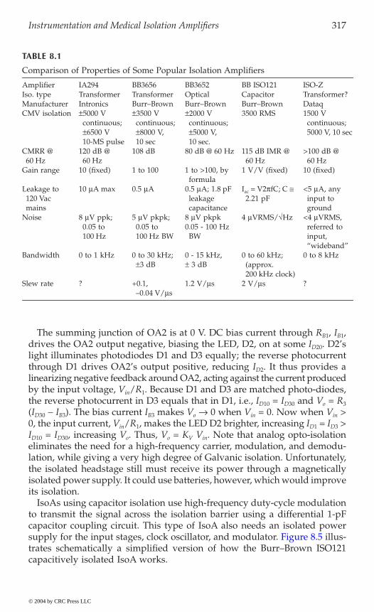
Instrumentation and Medical Isolation Amplifiers 317
The summing junction of OA2 is at 0 V. DC bias current through RB1, IB1,drives the OA2 output negative, biasing the LED, D2, on at some ID20. D2’slight illuminates photodiodes D1 and D3 equally; the reverse photocurrentthrough D1 drives OA2’s output positive, reducing ID2. It thus provides alinearizing negative feedback around OA2, acting against the current producedby the input voltage, Vin/R1. Because D1 and D3 are matched photo-diodes,the reverse photocurrent in D3 equals that in D1, i.e., ID10 = ID30 and Vo = R3
(ID30 - IB3). The bias current IB3 makes Vo Æ 0 when Vin = 0. Now when Vin >0, the input current, Vin/R1, makes the LED D2 brighter, increasing ID1 = ID3 >ID10 = ID30, increasing Vo. Thus, Vo = KV Vin. Note that analog opto-isolationeliminates the need for a high-frequency carrier, modulation, and demodu-lation, while giving a very high degree of Galvanic isolation. Unfortunately,the isolated headstage still must receive its power through a magneticallyisolated power supply. It could use batteries, however, which would improveits isolation.
IsoAs using capacitor isolation use high-frequency duty-cycle modulationto transmit the signal across the isolation barrier using a differential 1-pFcapacitor coupling circuit. This type of IsoA also needs an isolated power
trates schematically a simplified version of how the Burr–Brown ISO121capacitively isolated IsoA works.
TABLE 8.1
Comparison of Properties of Some Popular Isolation Amplifiers
Amplifier IA294 BB3656 BB3652 BB ISO121 ISO-ZIso. type Transformer Transformer Optical Capacitor Transformer?Manufacturer Intronics Burr–Brown Burr–Brown Burr–Brown DataqCMV isolation ±5000 V
continuous; ±6500 V 10-MS pulse
±3500 V continuous; ±8000 V, 10 sec
±2000 V continuous; ±5000 V, 10 sec.
3500 RMS 1500 V continuous; 5000 V, 10 sec
CMRR @ 60 Hz
120 dB @ 60 Hz
108 dB 80 dB @ 60 Hz 115 dB IMR @ 60 Hz
>100 dB @ 60 Hz
Gain range 10 (fixed) 1 to 100 1 to >100, by formula
1 V/V (fixed) 10 (fixed)
Leakage to 120 Vac mains
10 mA max 0.5 mA 0.5 mA; 1.8 pF leakage capacitance
Iac = V2pfC; C @ 2.21 pF
<5 mA, any input to ground
Noise 8 mV ppk; 0.05 to 100 Hz
5 mV pkpk; 0.05 to 100 Hz BW
8 mV pkpk0.05 - 100 Hz BW
4 mVRMS/÷Hz <4 mVRMS, referred to input, “wideband”
Bandwidth 0 to 1 kHz 0 to 30 kHz; ±3 dB
0 - 15 kHz,± 3 dB
0 to 60 kHz; (approx. 200 kHz clock)
0 to 8 kHz
Slew rate ? +0.1, –0.04 V/ms
1.2 V/ms 2 V/ms ?
© 2004 by CRC Press LLC
supply for the input stages, clock oscillator, and modulator. Figure 8.5 illus-

318 Analysis and Application of Analog Electronic Circuits
The positive signal Vin is added to a high-frequency symmetrical trianglewave, VT, with peak height, VpkT. The sum of VT and Vin is passed through acomparator, which generates a variable duty-cycle square wave, V2. Notethat the highest frequency in Vin is fc, the clock frequency, and Vinmax <Vpk. The state transitions in V2 are coupled through the two 1-pF capacitorsas spikes to a flip-flop on the output side of the IA. The flip-flop’s transitionsare triggered by the spikes. At the flip flop’s output, a ±V3m-variable duty-cycle square wave, V3, is then averaged by low-pass filtering to yield Vo.
The duty cycle of V2 and V3 can be shown to be:
(8.1)
The average of the symmetrical flip-flop output is:
(8.2)
FIGURE 8.3Simplified schematic of an Analog Device’s AD289 magnetically isolated isolation amplifier(IsoA). An AD620 IA is used as a differential front end for the IsoA; it is powered from theAD289’s isolated power supply.
OA
LPFPSDPSM
Isolatedpower supply
± 15 V
Poweroscillator
@ fc
Regulator
10 k
Vo
IA out
Out. ground
OA
dc power in
+
T2
T1
LPF
Rgain
Inputcommon
Gain setResistor
InputAnti-aliasing
Isolated± 15V out
Isolatedpower supply
± 15 V
h V T T V V V vin in pkT in pkT( ) ∫ = +( ) <+1
2 2 ,
V V V V Vo in m pkT= = ( )3 3
© 2004 by CRC Press LLC
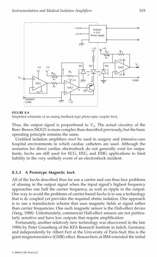
Instrumentation and Medical Isolation Amplifiers 319
Thus, the output signal is proportional to Vin. The actual circuitry of theBurr–Brown ISO121 is more complex than described previously, but the basicoperating principle remains the same.
Certified isolation amplifiers must be used in surgery and intensive-carehospital environments in which cardiac catheters are used. Although thescenarios for direct cardiac electroshock do not generally exist for outpa-tients, IsoAs are still used for ECG, EEG, and EMG applications to limitliability in the very unlikely event of an electroshock incident.
8.3.3 A Prototype Magnetic IsoA
All of the IsoAs described thus far use a carrier and can thus face problemsof aliasing in the output signal when the input signal’s highest frequencyapproaches one half the carrier frequency, as well as ripple in the output.One way to avoid the problems of carrier-based IsoAs is to use a technologythat is dc coupled yet provides the required ohmic isolation. One approachis to use a transduction scheme that uses magnetic fields at signal ratherthan carrier frequencies. One such magnetic sensor is the Hall-effect device(Yang, 1988). Unfortunately, commercial Hall-effect sensors are not particu-larly sensitive and have low outputs that require amplification.
Fortunately, another relatively new technology was discovered in the late1980s by Peter Gruenberg of the KFA Research Institute in Julich, Germany,and independently by Albert Fert at the University of Paris-Sud; this is thegiant magnetoresistive (GMR) effect. Researchers at IBM extended the initial
FIGURE 8.4Simplified schematic of an analog feedback-type photo-optic coupler IsoA.
D3D2D1
R1
Isolated± 15V
Power supply
+15
−15
OA2
Vo
Q1
−15λ λ
+15
RB1
+15
R2
+15
+15R3
+15
GND
−15
OA3
RB3
+15IB3
IB1
OA1
IsolatedGND
−15
Vin
© 2004 by CRC Press LLC
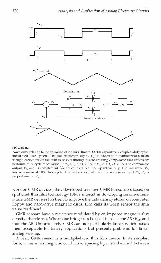
320 Analysis and Application of Analog Electronic Circuits
work on GMR devices; they developed sensitive GMR transducers based onsputtered thin film technology. IBM’s interest in developing sensitive min-iature GMR devices has been to improve the data density stored on computerfloppy and hard-drive magnetic discs. IBM calls its GMR sensor the spinvalve read-head.
GMR sensors have a resistance modulated by an imposed magnetic fluxdensity; therefore, a Wheatsone bridge can be used to sense the DR/RM, andthus the DB. Unfortunately, GMRs are not particularly linear, which makesthem acceptable for binary applications but presents problems for linearanalog sensing.
A basic GMR sensor is a multiple-layer thin film device. In its simplestform, it has a nonmagnetic conductive spacing layer sandwiched between
FIGURE 8.5Waveforms relating to the operation of the Burr–Brown ISO121 capacitively coupled, duty cycle-modulated IsoA system. The low-frequency signal, Vin, is added to a symmetrical 0-meantriangle carrier wave; the sum is passed through a zero-crossing comparator that effectivelyperforms duty-cycle modulation. If Vin > 0, T+/T > 0.5; if Vin < 0, T+/T < 0.5. The comparatoroutput, V2, and its complement, , are coupled to a flip-flop whose output square wave, V3,has zero mean at 50% duty cycle. The text shows that the time average value of V3, Vo, isproportional to Vin.
T
T+
t
t
t
V2
V3
V3m
T+
−V3mt
0
0
Vs
Vs
Lo
0
Vs
HiVin
V2
SFF−V2
VT
1 pFComparator
V3
VT
LPFVo
1 pF(Isolation capacitors)
VpkT
(Vin + VT)
V2
© 2004 by CRC Press LLC
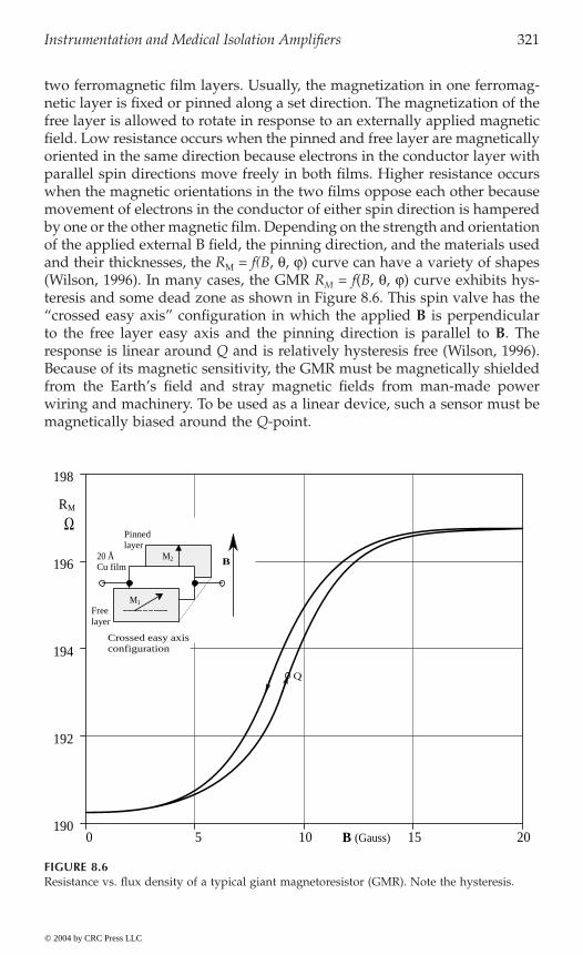
Instrumentation and Medical Isolation Amplifiers 321
two ferromagnetic film layers. Usually, the magnetization in one ferromag-netic layer is fixed or pinned along a set direction. The magnetization of thefree layer is allowed to rotate in response to an externally applied magneticfield. Low resistance occurs when the pinned and free layer are magneticallyoriented in the same direction because electrons in the conductor layer withparallel spin directions move freely in both films. Higher resistance occurswhen the magnetic orientations in the two films oppose each other becausemovement of electrons in the conductor of either spin direction is hamperedby one or the other magnetic film. Depending on the strength and orientationof the applied external B field, the pinning direction, and the materials usedand their thicknesses, the RM = f(B, q, j) curve can have a variety of shapes(Wilson, 1996). In many cases, the GMR RM = f(B, q, j) curve exhibits hys-teresis and some dead zone as shown in Figure 8.6. This spin valve has the“crossed easy axis” configuration in which the applied B is perpendicularto the free layer easy axis and the pinning direction is parallel to B. Theresponse is linear around Q and is relatively hysteresis free (Wilson, 1996).Because of its magnetic sensitivity, the GMR must be magnetically shieldedfrom the Earth’s field and stray magnetic fields from man-made powerwiring and machinery. To be used as a linear device, such a sensor must bemagnetically biased around the Q-point.
FIGURE 8.6Resistance vs. flux density of a typical giant magnetoresistor (GMR). Note the hysteresis.
RM
192
194
196
198
1900 5 10 15 20B (Gauss)
Pinnedlayer
Ω
Freelayer
Cu film B
Crossed easy axisconfiguration
M2
M1
20 Å
Q
© 2004 by CRC Press LLC

322 Analysis and Application of Analog Electronic Circuits
Much research is currently going on to improve the linearity and sensitivityof spin valves or GMR sensors. Attention is being paid to the use of multiplelayered thin films of various compositions, including two pinned layers; 6 to12 layers are being studied by Fujitsu (Kanai et al., 2001).
GMR sensors are available commercially. Infineon Technologies offers afour-element GMR IC package in which the four GMRs are connected in abridge. Their GMR B6 is intended as a rotary position sensor in that thebridge output is a sinusoidal function of the input magnet’s B field angle.The magnetic field-free value of each resistor is approximately 700 W.Rhopoint Components of Oxted, Surrey, U.K. offers a 12-sensor GMR devicekit for experimenters and research and development use.
The author’s version of a prototype IsoA design based on GM resistors is
bridge (Wilson). The bridge can be powered with dc or ac; if ac is used, aphase-sensitive rectifier must be placed between the DA and the integrator.The quantity under isolated measurement is transduced to Vs, which isconverted to a signal current, IS, by a VCCS with transconductance, GM. Adc bias current component, Iso, must be added to IS to move the operatingpoint of the GMR resistors to a linear region of its RM = f(B) curve. Thecurrent IS through the coils on the opposite diagonals of the bridge createsequal B fields, which cause identical changes in the GMRs, DRs, that, in turn,unbalance the bridge. The bridge output is amplified by the DA and servesas the input to an integrator. The integrator output causes a feedback current,IF, to flow that forces DRf = DRs in the other two diagonal RMs, which re-nullsthe bridge output. Because of symmetry, the feedback current IF = IS + Iso atnull and the output voltage of the op amp transresistor is:
Vo = -IF RF = -Vs GM RF + Iso RF (8.3)
Thus,
(8.4)
Galvanic isolation of the GMR bridge IsoA depends on the insulationbetween the chip containing the four GMR resistors and the two input coils.The capacitance between the coils and RMs and the dielectric breakdown ofthis insulation are important.
8.4 Safety Standards in Medical Electronic Amplifiers
8.4.1 Introduction
The central rationale for safety standards for medical electronic equipmentis based on the need to prevent harm to human patients and health-care
V I R V G Rs so F o M F= -( ) ( )
© 2004 by CRC Press LLC
shown in Figure 8.7. Four GMR resistors are connected as a Wheatstone
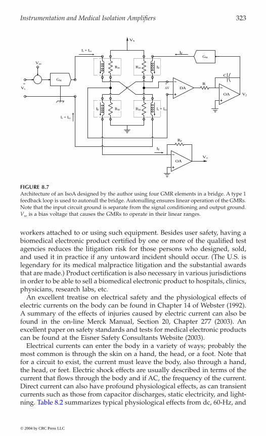
Instrumentation and Medical Isolation Amplifiers 323
workers attached to or using such equipment. Besides user safety, having abiomedical electronic product certified by one or more of the qualified testagencies reduces the litigation risk for those persons who designed, sold,and used it in practice if any untoward incident should occur. (The U.S. islegendary for its medical malpractice litigation and the substantial awardsthat are made.) Product certification is also necessary in various jurisdictionsin order to be able to sell a biomedical electronic product to hospitals, clinics,physicians, research labs, etc.
An excellent treatise on electrical safety and the physiological effects ofelectric currents on the body can be found in Chapter 14 of Webster (1992).A summary of the effects of injuries caused by electric current can also befound in the on-line Merck Manual, Section 20, Chapter 277 (2003). Anexcellent paper on safety standards and tests for medical electronic productscan be found at the Eisner Safety Consultants Website (2003).
Electrical currents can enter the body in a variety of ways; probably themost common is through the skin on a hand, the head, or a foot. Note thatfor a circuit to exist, the current must leave the body, also through a hand,the head, or feet. Electric shock effects are usually described in terms of thecurrent that flows through the body and if AC, the frequency of the current.Direct current can also have profound physiological effects, as can transientcurrents such as those from capacitor discharges, static electricity, and light-
FIGURE 8.7Architecture of an IsoA designed by the author using four GMR elements in a bridge. A type 1feedback loop is used to autonull the bridge. Autonulling ensures linear operation of the GMRs.Note that the input circuit ground is separate from the signal conditioning and output ground.Vso is a bias voltage that causes the GMRs to operate in their linear ranges.
+∆V DA
R
OA
GM
Vb
IF
V2
Vs
+
Is + Iso
RM Is + Iso
Is + Iso
Vso
Vo
OA
GM
C
RM RM IF
IF RM
IF
RF
© 2004 by CRC Press LLC
ning. Table 8.2 summarizes typical physiological effects from dc, 60-Hz, and

324 Analysis and Application of Analog Electronic Circuits
10-kHz electric currents in a macroshock scenario in which the current isapplied between the hands. The data are based on several sources, includinghuman and animal studies.
current path in humans. Plotted is the current vs. frequency for the medianof the test population; the bars show the 99.5 and 0.5 percentile limits. Thiscurve and the preceding table teach that power line frequency (50 or 60 Hz)is the most physiologically effective in producing electric shock damage tothe body and heart. Direct current and AC at 10 kHz are about one sixth aseffective in doing damage. Consequently, impedance pneumographs andplethysmographs typically pass mA level currents with frequencies ofapproximately 75 kHz through the chest with no untoward effects.
When the heart is stimulated directly, as in open-heart surgery or cardiacpacemaker catheterization, the scenario is called microshock. The 60-Hz cur-rent required to induce ventricular fibrillation can be as low as 20 mA indogs. In humans, microshock current causing fibrillation is on the order of80 to 600 mA (Webster, 1990, Chapter 14).
8.4.2 Certification Criteria for Medical Electronic Systems
The data presented show that it is extremely important to prevent harmfulcurrents from flowing into the body under macroshock conditions from anyamplifier connected to the body by electrodes, such as in ECG, EEG, EMG,EOG, etc. measurements. The U.S. has a number of regulatory and certifyingagencies that ensure medical electronic devices are safe, including :
• Food and Drug Administration (FDA)• National Fire Protection Agency (NFPA) and its National Electrical
Code (NEC)• American National Standards Institute/Association for the Advance-
ment of Medical Instrumentation (ANSI/AAMI ES1-1993)
TABLE 8.2
Physiological Effects in the Body of Electric Currents Introduced through the Hands
Current in mA60 Hz 10 kHz DC Effect
0 to 0.3 0 to 5 0 to 0.6 No sensation2 8 3.5 Slight tingling on hand1 11 6 “Shock”; not painful10 51 58 Painful muscle spasms; recipient may let go20 60 65 Painful; muscle tetanus; recipient cannot let go>100 >500 Deep burns, edema, cardiac fibrillation, respiratory paralysis>2000 >2000 All of the above; death
Note: A current ¥ time product determines tissue damage once the power density in tissuesreaches the level at which temperatures rise to a level at which “cooking” occurs. Valuesare “typical” and can vary widely among individuals due to fat, muscle mass, etc.
© 2004 by CRC Press LLC
Figure 8.8 illustrates let-go current vs. frequency for the hand-to-hand
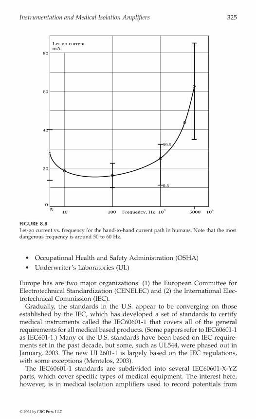
Instrumentation and Medical Isolation Amplifiers 325
• Occupational Health and Safety Administration (OSHA)• Underwriter’s Laboratories (UL)
Europe has are two major organizations: (1) the European Committee forElectrotechnical Standardization (CENELEC) and (2) the International Elec-trotechnical Commission (IEC).
Gradually, the standards in the U.S. appear to be converging on thoseestablished by the IEC, which has developed a set of standards to certifymedical instruments called the IEC60601-1 that covers all of the generalrequirements for all medical based products. (Some papers refer to IEC60601-1as IEC601-1.) Many of the U.S. standards have been based on IEC require-ments set in the past decade, but some, such as UL544, were phased out inJanuary, 2003. The new UL2601-1 is largely based on the IEC regulations,with some exceptions (Mentelos, 2003).
The IEC60601-1 standards are subdivided into several IEC60601-X-YZparts, which cover specific types of medical equipment. The interest here,however, is in medical isolation amplifiers used to record potentials from
FIGURE 8.8Let-go current vs. frequency for the hand-to-hand current path in humans. Note that the mostdangerous frequency is around 50 to 60 Hz.
80
60
40
20
05
5000Frequency, Hz10 100 103 104
0.5
99.5
Let-go currentmA
© 2004 by CRC Press LLC

326 Analysis and Application of Analog Electronic Circuits
the body surface. Four classes of basic electrical safety tests are defined bythe IEC. These include:
• Protective earth verification: ground continuity test; ground bond test• Dielectric strength: AC hipot test; DC hipot test• High resistance: insulation resistance test• Leakage current: Earth leakage, touch/chassis (enclosure); patient
leakage and patient auxiliary leakage
The earth (ground or green wire) verification test passes 25 amps from theline cord plug ground (green) terminal to the chassis, to ensure cord-to-chassis ground connection robustness, and measures the voltage betweenthe current source and the chassis or cabinet. The resistance of the groundingsystem must be <0.1 W for a detachable line cord and <0.2 W for a fixed cordaccording to IEC60601-1 specifications. Resistance is calculated by Ohm’slaw: R = V/25 ohms.
The dielectric strength test applies a high ac or dc voltage to the line powerinput to ensure that no insulation breakdown or flashover (arcing) occursbetween ground and the input power line with both terminals tied together.The basic IEC60601-1 standard requires the DUT to withstand 1250 VRMSat 60 Hz for 1 min. Medical isolation amplifiers easily exceed this require-
Vpk, 60 Hz continuous from patient inputs to the outputs/power common.The IA175 runs on +15 VDC, so further isolation can be obtained by usinga medical-grade power supply that meets IEC60601-1 standards.
The insulation resistance test is a voltmeter–ammeter test of the DUT’sinsulation using a high-voltage DC source. For example, a high DC potentialis applied to the IsoA’s power input common, e.g., 1000 V, and the steady-state current to ground is measured at the isolated power supply’s neutral.Such current would be 1 nA DC if the resistance were 1012 W .
Finally, leakage currents are considered. The four types of leakage currentdefined by the IEC as described by Eisner (2001) are:
Earth leakage: the most important and most common of the line leakagecurrent tests, earth leakage current is basically the current flowing backthrough the ground conductor on the power cord [green wire]. It ismeasured by opening the ground conductor, inserting a circuit with thesimulated impedance of the human body and measuring the voltageacross part of the circuit with a true RMS voltmeter.
Patient leakage: a line leakage current test that measures the current thatwould flow from or to applied parts such as sensor and patient leads.
Patient auxiliary leakage: that line leakage current flowing in the patientin NORMAL use between applied parts of the DUT and not intended toproduce a physiological effect.
© 2004 by CRC Press LLC
ment (see Table 8.1). For example, the Intronics IA175 IsoA is rated at 3000
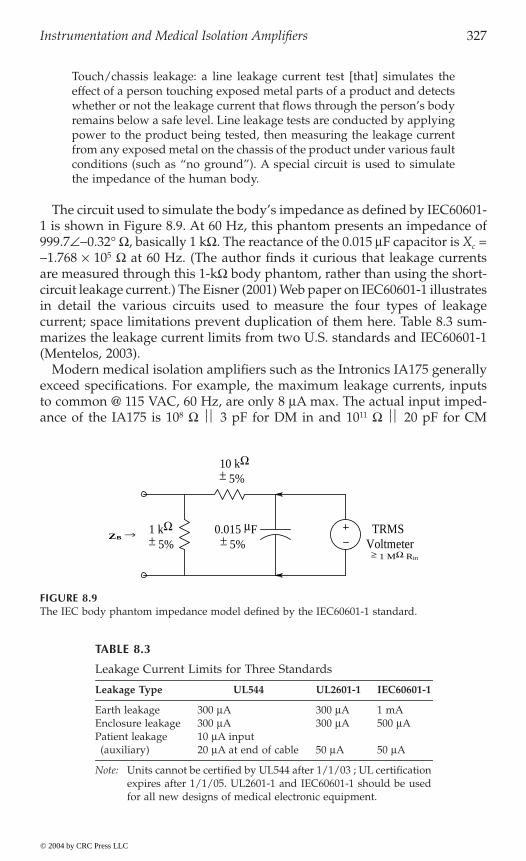
Instrumentation and Medical Isolation Amplifiers 327
Touch/chassis leakage: a line leakage current test [that] simulates theeffect of a person touching exposed metal parts of a product and detectswhether or not the leakage current that flows through the person’s bodyremains below a safe level. Line leakage tests are conducted by applyingpower to the product being tested, then measuring the leakage currentfrom any exposed metal on the chassis of the product under various faultconditions (such as “no ground”). A special circuit is used to simulatethe impedance of the human body.
The circuit used to simulate the body’s impedance as defined by IEC60601-1 is shown in Figure 8.9. At 60 Hz, this phantom presents an impedance of999.7-0.32∞ W, basically 1 kW. The reactance of the 0.015 mF capacitor is Xc =-1.768 ¥ 105 W at 60 Hz. (The author finds it curious that leakage currentsare measured through this 1-kW body phantom, rather than using the short-circuit leakage current.) The Eisner (2001) Web paper on IEC60601-1 illustratesin detail the various circuits used to measure the four types of leakagecurrent; space limitations prevent duplication of them here. Table 8.3 sum-marizes the leakage current limits from two U.S. standards and IEC60601-1(Mentelos, 2003).
Modern medical isolation amplifiers such as the Intronics IA175 generallyexceed specifications. For example, the maximum leakage currents, inputsto common @ 115 VAC, 60 Hz, are only 8 mA max. The actual input imped-ance of the IA175 is 108 W ÔÁ 3 pF for DM in and 1011 W ÔÁ 20 pF for CM
FIGURE 8.9The IEC body phantom impedance model defined by the IEC60601-1 standard.
TABLE 8.3
Leakage Current Limits for Three Standards
Leakage Type UL544 UL2601-1 IEC60601-1
Earth leakage 300 mA 300 mA 1 mAEnclosure leakage 300 mA 300 mA 500 mAPatient leakage(auxiliary)
10 mA input20 mA at end of cable 50 mA 50 mA
Note: Units cannot be certified by UL544 after 1/1/03 ; UL certificationexpires after 1/1/05. UL2601-1 and IEC60601-1 should be usedfor all new designs of medical electronic equipment.
10 kΩ± 5%
1 kΩ± 5%
0.015 µF± 5%
TRMSVoltmeter
ZB →
≥ 1 MΩ Rin
© 2004 by CRC Press LLC
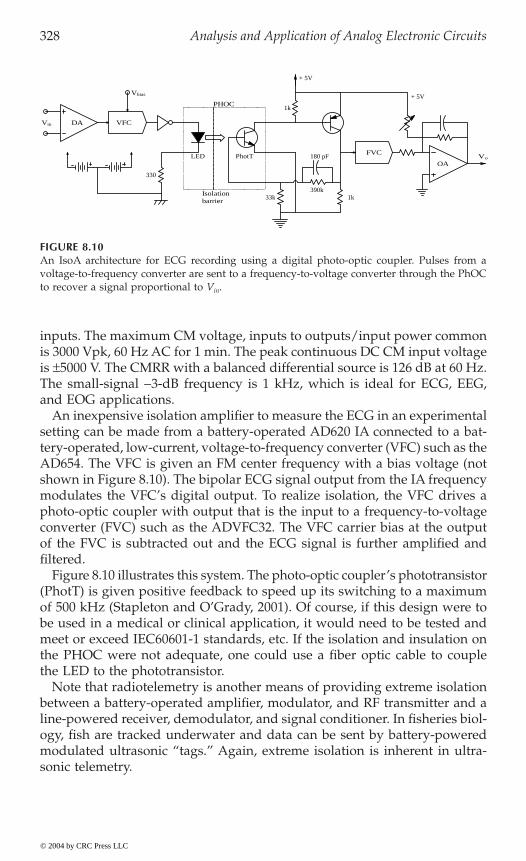
328 Analysis and Application of Analog Electronic Circuits
inputs. The maximum CM voltage, inputs to outputs/input power commonis 3000 Vpk, 60 Hz AC for 1 min. The peak continuous DC CM input voltageis ±5000 V. The CMRR with a balanced differential source is 126 dB at 60 Hz.The small-signal -3-dB frequency is 1 kHz, which is ideal for ECG, EEG,and EOG applications.
An inexpensive isolation amplifier to measure the ECG in an experimentalsetting can be made from a battery-operated AD620 IA connected to a bat-tery-operated, low-current, voltage-to-frequency converter (VFC) such as theAD654. The VFC is given an FM center frequency with a bias voltage (notshown in Figure 8.10). The bipolar ECG signal output from the IA frequencymodulates the VFC’s digital output. To realize isolation, the VFC drives aphoto-optic coupler with output that is the input to a frequency-to-voltageconverter (FVC) such as the ADVFC32. The VFC carrier bias at the outputof the FVC is subtracted out and the ECG signal is further amplified andfiltered.
Figure 8.10 illustrates this system. The photo-optic coupler’s phototransistor(PhotT) is given positive feedback to speed up its switching to a maximumof 500 kHz (Stapleton and O’Grady, 2001). Of course, if this design were tobe used in a medical or clinical application, it would need to be tested andmeet or exceed IEC60601-1 standards, etc. If the isolation and insulation onthe PHOC were not adequate, one could use a fiber optic cable to couplethe LED to the phototransistor.
Note that radiotelemetry is another means of providing extreme isolationbetween a battery-operated amplifier, modulator, and RF transmitter and aline-powered receiver, demodulator, and signal conditioner. In fisheries biol-ogy, fish are tracked underwater and data can be sent by battery-poweredmodulated ultrasonic “tags.” Again, extreme isolation is inherent in ultra-sonic telemetry.
FIGURE 8.10An IsoA architecture for ECG recording using a digital photo-optic coupler. Pulses from avoltage-to-frequency converter are sent to a frequency-to-voltage converter through the PhOCto recover a signal proportional to Vin.
PHOC
330
33k
1k
1k390k
Isolationbarrier
+ 5V
+ 5V
LED
Vbias
VFCDAVin
FVC
OA180 pFPhotT Vo
© 2004 by CRC Press LLC

Instrumentation and Medical Isolation Amplifiers 329
8.5 Medical-Grade Power Supplies
The only practical way to achieve extreme galvanic isolation and still couplesignificant power from the mains to a low-voltage regulated dc supply thatpowers a medical amplifier is by toroidal transformer. The transformer canoperate at line frequency or, for lighter weight and improved efficiency, canoperate at frequencies in the 10- to 100-kHz range. A power oscillator mustbe used to drive the transformer’s primary in the latter case. If a high-frequency oscillator is used, the transformer can be made smaller and lighter(a smaller core and fewer turns on the windings are required) and the outputfilter capacitor can be smaller and lighter.
A toroidal transformer is used for efficiency in magnetic coupling theprimary to secondary windings; the toroidal core allows the primary andsecondary to be separate physically on the core to minimize capacitive cou-pling between them. By physically separating the windings and insulatingthem from the core with special insulation, breakdown voltages betweenprimary and secondary can be made 8 kV or greater and primary-to-secondarydc resistance can be on the order of 1012 W and greater. The secondary acvoltage is rectified by the usual means; the raw dc is low-pass filtered by acapacitor, and then regulated by a feedback regulator. The net result is a dcsupply with guaranteed extreme galvanic isolation between the input powerlines (high, low, and ground) and the output dc terminals (ground and VCC).
Many power supply manufacturers make medical grade units; for example,
alone power supplies including wall plug-in “bricks” and open-frame units.Their class II double insulated units withstand 4 kV ac or 5.65 kV dcinput–output potential and have less than 100-mA leakage.
8.6 Chapter Summary
This chapter described the properties and uses of instrumentation amplifierICs, including those that can be made from low-noise op amps. Requirementsfor and properties of medical isolation amplifiers were also examined. Galvanicisolation is required for patient safety in all settings (surgical, clinical, out-patient). Power supply isolation is achieved by batteries or special trans-former-coupled power supplies. Isolation amplifier analog output must alsobe isolated. One way this can be done is by DSBSC modulation of a high-frequency ac carrier by the physiological signal, and coupling the modulatedcarrier to the output with a transformer, where the signal is recovered witha demodulator.
© 2004 by CRC Press LLC
GlobTek Inc. (www.globtek.com) offers a broad line of medical-grade, stand-

330 Analysis and Application of Analog Electronic Circuits
Another way of coupling the physiological signal to the output with iso-lation is to use a photo-optic coupler and transmit the signal directly in
signal is sampled and converted by a serial output analog-to-digital converter,the digital output can also be transmitted through a digital photo-opticcoupler to the output. Still another way of coupling an isolated signal to theoutput was by converting the signal to a pulse-width modulated (PWM)TTL square wave and coupling this wave to the output with two 1-pFcapacitors. At the output, this wave is highly differentiated into a spike train.Flip-flops recover the PWM wave at the output and the signal is demodu-lated by averaging.
The physiological effects of electroshock were described, includinginduced cardiac fibrillation, apnea, and burns. Certification agencies formedical electronic devices worldwide were listed and some of their stan-dards compared. The U.S. was seen to have five major certifying agencies;Europe had two. A trend in the U.S. is to converge on the IEC standards. Tomeet European marketing standards for medical electronic devices, U.S.manufacturers must meet IEC and CENELEC standards that, paradoxicallyin some areas, are less stringent than NFPA and other U.S. standards.
Finally, medical-grade power supplies that run off the mains were discussed.
© 2004 by CRC Press LLC
analog form (see Section 6.6.4 of Chapter 6). If the isolated physiological
331
9Noise and the Design of Low-Noise Amplifiers for Biomedical Applications
9.1 Introduction
The noise considered in this chapter provides one limitation to the precisionof biomedical measurements. Other factors that limit resolution are the dis-tortion caused by signal conditioning system nonlinearity and quantizationin the analog-to-digital conversion (ADC) of input signals. The degree towhich a biosignal is resolvable can be determined by the signal-to-noise ratioat the output of the signal conditioning system. The noise in this chapter isconsidered to arise in a circuit, measurement system, or electrode fromcompletely random processes. Although any physical quantity can be"noisy,” this chapter will generally consider only completely random noisevoltages and currents; these will be defined as being stationary (the physicalprocess giving rise to the noise does not change with time) and having zeromean (zero additive dc components). An unwanted dc component accom-panying a noise source in practice can be from an electrochemical EMFarising in a recording electrode or from amplifier dc offset voltage or biascurrent. The reduction of unwanted dc components will not be treated here.
Coherent interference (CI) can also be present at the output of biomedicalsignal conditioning systems. As its name suggests, CI generally has its originsin periodic, manmade phenomena, such as power line-frequency electric andmagnetic fields; radio-frequency sources such as radio and television broad-cast antennas; certain poorly shielded computer equipment; spark dischargephenomena such as automotive ignitions and electric motor brushes andcommutators; and inductive switching transients generated by SCR motorspeed controls, etc. It is well known that minimization of CI is often “arty”and may involve changing the grounding circuits for a system; shieldingwith magnetic and/or electric conducting materials; filtering; using isolationtransformers, etc. (Northrop, 1997, Section 3.9). In this chapter, however,attention will be focused on purely random, stationary, incoherent noise.
Minimizing the impact of incoherent noise in a measurement system ofteninvolves a prudent choice of low-noise amplifiers and components, certain
© 2004 by CRC Press LLC
332 Analysis and Application of Analog Electronic Circuits
basic electronic design principles, and band-pass filtering. First, commonlyused methods for describing stationary random noise will be examined.
9.2 Descriptors of Random Noise in Biomedical Measurement Systems
9.2.1 Introduction
When stationarity is assumed for a noise source, averages over time areequivalent to ensemble averages. An ensemble average is carried out at agiven time on data from N separate records that are generated simulta-neously from a stationary random process (SRP) (in the limit N Æ •). If thestationary random process is ergodic, then only one record needs to beexamined statistically because it is “typical” of all N records from the SRP.
An example of a nonstationary noise source is a resistor that, at time t = 0,begins to dissipate average power such that its temperature slowly risesabove ambient, as does its resistance. (As demonstrated later, the mean-squared noise voltage from a resistor is proportional to its Kelvin temperature.)
Probability and statistics are used to describe random phenomena. Severalstatistical methods for describing random noise include but are not limitedto the mean; the root-mean-square (RMS) value; the probability densityfunction; the cross- and autocorrelation functions and their Fourier trans-forms; the cross- and autopower density spectra (PDS); and the root powerdensity spectrum (RPS, which is simply the square root of the PDS). ThePDS and RPS are, in general, functions of frequency. These descriptors aretreated in detail next.
9.2.2 The Probability Density Function
The probability density function (PDF) is a mathematical model thatdescribes the probability that any random sample of a noise function, n(t),will lie in a certain range of values. The univariate PDF considers only theamplitude statistics of the noise waveform, not how it varies in time. Theunivariate PDF of the SRV, n(t), is defined as:
(9.1)
where x is a specific value of n taken at some time, t, and dx is a differentialincrement in x. The mathematical basis for many formal derivations andproofs in probability theory, the PDF has the properties:
p xx n x dx
dx( ) ∫ < £ +( )[ ]Probability that
© 2004 by CRC Press LLC
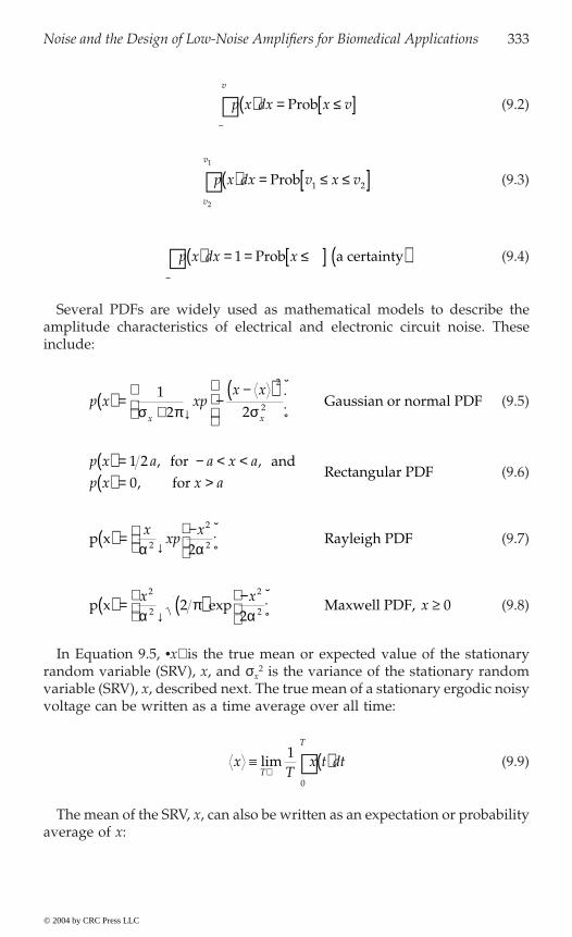
Noise and the Design of Low-Noise Amplifiers for Biomedical Applications 333
(9.2)
(9.3)
(9.4)
Several PDFs are widely used as mathematical models to describe theamplitude characteristics of electrical and electronic circuit noise. Theseinclude:
(9.5)
(9.6)
(9.7)
(9.8)
In Equation 9.5, ·xÒ is the true mean or expected value of the stationaryrandom variable (SRV), x, and sx
2 is the variance of the stationary randomvariable (SRV), x, described next. The true mean of a stationary ergodic noisyvoltage can be written as a time average over all time:
(9.9)
The mean of the SRV, x, can also be written as an expectation or probabilityaverage of x:
p x dx x vv
( ) = £[ ]-•Ú Prob
p x dx v x vv
v
( ) = £ £[ ]Ú2
1
1 2Prob
p x dx x( ) = = £ •[ ] ( )-•
•
Ú 1 Prob a certainty
p x xpx x
x x
( ) =÷
Ê
ËÁˆ
¯-
-( )È
ÎÍÍ
˘
˚˙˙
12 2
2
2s p sGaussian or normal PDF
p x a a x a
p x x a( ) = - < <( ) = >
1 20
, ,,
for and for
Rectangular PDF
p x Rayleigh PDF( ) = ÊËÁ
ˆ¯
-È
ÎÍ
˘
˚˙
xxp
xa a2
2
22
p x Maxwell PDF, ( ) =ÊËÁ
ˆ¯
( ) -È
ÎÍ
˘
˚˙ ≥x x
x2
2
2
222
0a
pa
exp
xT
x t dtT
T
∫ ( )Æ • Úlim
1
0
© 2004 by CRC Press LLC
334 Analysis and Application of Analog Electronic Circuits
(9.10)
Similarly, the mean squared value of x can be expressed by the expectationor probability average of x2:
(9.11)
The mean can be estimated by a finite average over time. For discrete data,this is called the sample mean, which is a statistical estimate of the true meanand as such has noise itself.
(9.12)
The variance of the random noise, sx2, is defined by:
(9.13)
It easy to show from this equation that ·x2Ò = sx2 + ·xÒ2, or Ex2 = sx
2 + E2x.Because the random noise to be considered has zero mean, the mean squarednoise is also its variance.
Under most conditions, it is assumed that the random noise arising in abiomedical measurement system has a Gaussian PDF. Many mathematicalbenefits follow this assumption; for example, the output of a linear systemis Gaussian with variance sy
2 given the input to be Gaussian with variancesx
2. If Gaussian noise passes through a nonlinear system, the output PDFgenerally will not be Gaussian; however, this chapter will show ways ofdescribing the transformation of Gaussian input noise by a nonlinear system.
9.2.3 The Power Density Spectrum
A noise source can be thought of as the sum of a very large number of sinewave sources with different amplitudes, phases, and frequencies. Very heu-ristically, a power density spectrum (PDS) shows how the mean squaredvalues of these sources is distributed in frequency.
E x x p x dx x ∫ ( ) =-•
•
Ú
E v v p v dv v2 2 2 ∫ ( ) =-•
•
Ú
xT
x t dt xN
xT
kk
N
= ( ) = ( )Ú Â=
1 1
0 1
, or sample mean
sx T
T
E x x x x p x dxT
x t x dt2 2 2 2
0
1∫ -[ ] = -[ ] ( ) = ( ) -[ ]-•
•
Æ •Ú Úlim
© 2004 by CRC Press LLC
Noise and the Design of Low-Noise Amplifiers for Biomedical Applications 335
One approach to illustrate the meaning of the PDS of the noise, n(t),uses the autocorrelation function (ACF) of the noise. The ACF is definedin the following by the continuous time integral (Aseltine, 1958):
(9.14)
The two-sided PDS is the continuous Fourier transform (CFT) of theautocorrelation function of the noise:
(9.15)
Because Rnn(t) is an even function, its Fourier transform, Fnn(w), is alsoan even function; stated mathematically, this means:
Fnn(w) = Fnn(-w) (9.16)
The following discussion will also consider the one-sided PDS, Sn( f ),which is related to the two-sided PDS by:
Sn( f ) = 2 Fnn(2p f ) for f ≥ 0 (9.17)
and
Sn( f ) = 0 for f < 0. (9.18)
Note that the radian frequency, w, is related to the Hertz frequency simplyby w = 2pf.
To see how to find the one-sided PDS experimentally, examine the
an ideal low-pass filter with an adjustable cut-off frequency, fc. The output ofthe ideal low-pass filter is measured with a broadband, true RMS, AC volt-meter. Begin with fc = 0 and systematically increase fc, each time recordingthe square of the RMS meter reading, which is the mean squared outputvoltage, , of the filter. As fc is increased, increases monotonically, asshown in Figure 9.1(B). Because of the finite bandwidth of the noise source,
eventually reaches an upper limit, which is the total mean-squared noisevoltage of the noise source. The plot of vs. fc is called the cumulativemean-squared noise characteristic of the noise source. In this example, itsunits are mean-squared volts.
RT
n t n t dtT
n t n t dtnn TT
T
TT
T
t t t( ) = ( ) +( ) = -( ) ( )Æ •
-Æ •
-Ú Úlim lim
12
12
Fnn nnjR e dw
pt twt( ) = ( ) -
-•
•
Ú12
von2 von
2
von2
von2 fc( )
© 2004 by CRC Press LLC
model system shown in Figure 9.1(A). Here, a noise voltage is the input to

336 Analysis and Application of Analog Electronic Circuits
A simple interpretation of the one-sided noise power density spectrum,Sn(f ), is that it is the derivative, or slope, of the cumulative mean-squarednoise characteristic curve described previously. Stated mathematically, thisis:
(9.19)
FIGURE 9.1(A) System for measuring the integral power spectrum (cumulative mean-squared noise char-acteristic) of a noise voltage source, eN( f ). (B) Plot of a typical integral power spectrum. (C) Plotof a typical one-sided power density spectrum. See text for description.
True RMSvoltmeter
Ideal, variable LPF
fc0
0f
1
eN von
fc (Hz)0
0
_____
von2
Sn(f)
f
00
C
B
A
(MSV/Hz)
(MSV)
_______
von2(fc)
von /eN
S fd v f
dffn
on( ) ∫ ( ) £ £ •2
, 0 mean squared volts hertz
© 2004 by CRC Press LLC
Noise and the Design of Low-Noise Amplifiers for Biomedical Applications 337
PDS drops off to zero as f Æ •.Those first encountering the PDS concept sometimes ask why it is called
a power density spectrum. The power concept has its origin in the consid-eration of noise in communication systems and has little meaning in thecontext of noise in biomedical instrumentation systems. One way to ratio-nalize the power term is to consider an ideal noise voltage source with a1-ohm load. In this case, the average power dissipated in the resistor issimply the total mean-squared noise voltage (P = /R).
From the preceding heuristic definition of the PDS, it is possible to writethe total mean-squared voltage in the noise voltage source as the integral ofthe one-sided PDS:
(9.20)
The mean squared voltage in the frequency interval, (f1, f2), is found by:
(9.21)
Often noise is specified or described using root power density spectra,which are simply plots of the square root of Sn(f ) vs. f, and have the unitsof RMS volts (or other units) per root Hertz.
Special (ideal) PDSs are used to model or approximate portions of realPDSs. These include the White noise PDS and the one-over-f PDS. A white
that
(9.22)
which is clearly not realistic. A 1/f PDS is shown in Figure 9.2(B). The 1/fspectrum is often used to approximate the low-frequency behavior of realPDSs. Physical processes that generate 1/f-like noise include ionic surfacephenomena associated with electrochemical electrodes; carbon compositionresistors carrying direct current (metallic resistors are substantially free of1/f noise); and interface imperfections affecting diffusion and recombinationphenomena in semiconductor devices. The presence of 1/f noise can presentproblems in the electronic signal conditioning systems used for low-level,low-frequency, and dc measurements.
von2
v S f dfon n2
0
= ( )•
Ú
v f f S f dfon n
f
f
21 2
1
2
,( ) = ( )Ú mean squared volts
S f dfnw ( ) = ••
Ú0
© 2004 by CRC Press LLC
A plot of a typical noise PDS is shown in Figure 9.1(C). Note that a practical
noise PDS is shown in Figure 9.2(A). Note that this PDS is flat; this implies
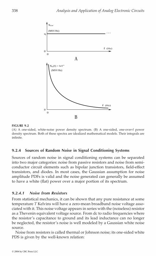
338 Analysis and Application of Analog Electronic Circuits
9.2.4 Sources of Random Noise in Signal Conditioning Systems
Sources of random noise in signal conditioning systems can be separatedinto two major categories: noise from passive resistors and noise from semi-conductor circuit elements such as bipolar junction transistors, field-effecttransistors, and diodes. In most cases, the Gaussian assumption for noiseamplitude PDFs is valid and the noise generated can generally be assumedto have a white (flat) power over a major portion of its spectrum.
9.2.4.1 Noise from Resistors
From statistical mechanics, it can be shown that any pure resistance at sometemperature T Kelvins will have a zero-mean broadband noise voltage asso-ciated with it. This noise voltage appears in series with the (noiseless) resistoras a Thevenin equivalent voltage source. From dc to radio frequencies wherethe resistor’s capacitance to ground and its lead inductance can no longerbe neglected, the resistor’s noise is well modeled by a Gaussian white noisesource.
Noise from resistors is called thermal or Johnson noise; its one-sided whitePDS is given by the well-known relation:
FIGURE 9.2(A) A one-sided, white-noise power density spectrum. (B) A one-sided, one-over-f powerdensity spectrum. Both of these spectra are idealized mathematical models. Their integrals areinfinite.
A
B
f (Hz)
f (Hz)
Sn(f) = b/f n
(MSV/Hz)
(MSV/Hz)
SnW
η . . .
00
00
© 2004 by CRC Press LLC

Noise and the Design of Low-Noise Amplifiers for Biomedical Applications 339
Sn(f ) = 4kTR mean squared volts/Hertz (9.23)
where k is Boltzmann’s constant (1.380 ¥ 10–23 joule/Kelvin), T is in degreesKelvin, and R is in ohms. In a given noise bandwidth, B = f2 - f1, the meansquared white noise from a resistor can be written:
(9.24)
A Norton equivalent of the Thevenin Johnson noise source from a resistorcan be formed by assuming an MS, white noise, short-circuit current sourcewith PDS:
Sni(f ) = 4kTG MS amps/Hz (9.25)
This Norton noise current root spectrum, in RMS A/÷Hz, is in parallel witha noiseless conductance, G = 1/R.
The Johnson noise from several resistors connected in a network may becombined into a single Thevenin noise voltage source in series with a single
for two-terminal circuits.It has been observed that when dc (or average) current is passed through
a resistor, the basic Johnson noise PDS is modified by the addition of a low-frequency, 1/f spectral component, e.g.,
Sn(f ) = 4kTR + A I 2/f MSV/Hz (9.26)
where I is the average or dc component of current through the resistor andA is a constant that depends on the material from which the resistor isconstructed (e.g., carbon composition, resistance wire, metal film, etc.).
An important parameter for resistors carrying average current is the cross-over frequency, fc, where the 1/f PDS equals the PDS of the Johnson noise.fc is easily shown to be:
fc = A I 2/4kTR Hz (9.27)
It is possible to show that the fc of a noisy resistor can be reduced by usinga resistor of the same type, but with a higher wattage or power dissipation
which a single resistor of R ohms, carrying a dc current I, is replaced by nineresistors of resistance R connected in a series-parallel circuit that also carriesthe current I. The nine-resistor circuit has a net resistance, R, which dissipatesnine times the power of the single resistor R. The noise PDS in any one ofthe nine resistors is:
v B S f df kTR f f kTRBon n
f
f
22 1
1
2
4 4( ) = ( ) = -( ) =Ú MSV
© 2004 by CRC Press LLC
noiseless equivalent resistor. Figure 9.3 illustrates some of these reductions
rating. As an example of this principle, consider the circuit of Figure 9.4 in
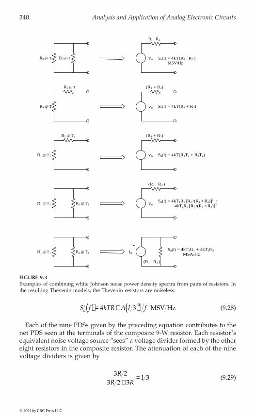
340 Analysis and Application of Analog Electronic Circuits
(9.28)
Each of the nine PDSs given by the preceding equation contributes to thenet PDS seen at the terminals of the composite 9-W resistor. Each resistor’sequivalent noise voltage source “sees” a voltage divider formed by the othereight resistors in the composite resistor. The attenuation of each of the ninevoltage dividers is given by
(9.29)
FIGURE 9.3Examples of combining white Johnson noise power density spectra from pairs of resistors. Inthe resulting Thevenin models, the Thevenin resistors are noiseless.
R1 R2
R2 @ TR1 @ T vn
vn
vn
R1 @ T1
(R1 + R2)R2 @ T
R1 @ T vn Sn(f) = 4kT(R1 + R2)
Sn(f) = 4kT(R1 R2 )
Sn(f) = 4kT(R1T1 + R2T2)
R2 @ T2 (R1 + R2)
R2 @ T2
(R1 R2 )
Sn(f) = 4kT1R1 [R2 /(R1 + R2)]2 +
4kT2R2 [R1 /(R1 + R2)]2R1 @ T1
(R1 R2 )
R1 @ T1 inR2 @ T2Sn(f) = 4kT1G1 + 4kT2G2
MSA/Hz
MSV/Hz
¢ ( ) = + ( )S f kTR A I fn 4 32
MSV Hz
3 23 2 3
1 3R
R R+=
© 2004 by CRC Press LLC
Noise and the Design of Low-Noise Amplifiers for Biomedical Applications 341
The net voltage PDS at the composite resistor’s terminals may only befound by superposition of MS voltages or PDSs:
(9.30)
Thus, the composite 9-W resistor enjoys a ninefold reduction in the 1/fspectral energy because the dc current density through each element isreduced by one third. The Johnson noise PDS remains the same, however.It is safe to generalize that the use of high wattage resistors of a given typeand resistance will result in reduced 1/f noise generation when the resistorcarries dc (average) current. The cost of this noise reduction is the extravolume required for a high-wattage resistor and its extra expense.
9.2.4.2 The Two-Source Noise Model for Active Devices
Noise arising in JFETs, BJTs, and complex IC amplifiers is generally describedby the two-noise source input model. The total noise observed at the outputof an amplifier, given that its input terminals are short-circuited, is accountedfor by defining an equivalent short-circuited input noise voltage, ena, whichreplaces the combined effect of all internal noise sources seen at the ampli-fier’s output under short-circuited input conditions. The amplifier, shown
na is specified by manufacturersfor many low-noise discrete transistors and IC amplifiers. ena is a root PDS,i.e., it is the square root of a one-sided PDS and is thus a function of fre-quency; ena
a plot of a typical ena(f ) vs. f for a low-noise JFET. Also shown in Figure 9.6is a plot of ina(f ) vs. f for the same device.
FIGURE 9.4Nine identical resistors in series parallel have the same resistance as any one resistor, and ninetimes the wattage.
All resistors R @ T
S f kTR A I f kTR A I fnj
9
2 2
1
924 3 1 3 4 9( )
=
( ) = + ( )[ ]( ) = +Â MSV Hz
© 2004 by CRC Press LLC
in Figure 9.5, is now considered noiseless. e
has the units of RMS volts per root Hertz. Figure 9.6 illustrates
342 Analysis and Application of Analog Electronic Circuits
In addition to the equivalent short-circuited input noise voltage, the mod-eling of the net noise characteristics of amplifiers requires the inclusion ofan equivalent input noise current source, ina, as shown in Figure 9.5. ina(f ) isthe root PDS of the input equivalent noise current; its units are RMS ampsper ÷Hertz. Note that ena(f ) and ina(f ) have flat mid-frequency portions thatinvite approximation by white noise sources. At high frequencies, bothequivalent noise root PDSs slope upward. For discrete JFETs and BJTs, andIC amplifiers, ena(f ) shows a distinct 1/÷f region at low frequencies.
9.2.4.3 Noise in JFETs
Certain selected discrete JFETs are sometimes used in the design of low-noiseamplifier headstages for biomedical signal conditioning systems. Some JFETsgive good low-noise performance in the audio and subaudio frequencyregions of the spectrum; others excel in the video and radio-frequency endof the spectrum, giving them applications for RF oscillators, mixers, and
FIGURE 9.5The two-noise source model for a noisy amplifier. ena and ina are root power density spectra.Rout is neglected.
FIGURE 9.6Plots of the ena and ina root power density spectra vs. f for a typical low-noise FET headstageamplifier. Note that ena has a low frequency 1/÷f component and ina does not. ina and ena increaseat very high frequencies.
Rs @ T
Vs R1 @ T ina
rmsA/√Hz
ena
Vi H(s)
Vi Vo
+
0
10
20
30
nVrms/√Hz
ena
ena
inafArms/√Hz
0
10
20
30
ina
f (Hz)10 1021 1 03 104 105 106 107
white region of ena
© 2004 by CRC Press LLC
Noise and the Design of Low-Noise Amplifiers for Biomedical Applications 343
tuned amplifiers used in ultrasound applications. Amplifiers using JFETheadstages have relatively low input dc bias currents (IB ª 10 pA) and highinput resistances (>1010 W), both of which are desirable.
Van der Ziel (1974) showed that the theoretical thermal noise generatedin the conducting channel of a JFET can be approximated by a white, equiv-alent short-circuited input noise with PDS given by:
(9.31)
where gm0 is the FET’s small-signal transconductance measured when VGS =0 and ID = IDSS; IDSS = the dc drain current measured for VGS = 0 and VDS >VP; and IDQ = the quiescent dc drain current at the FET’s operating pointwhere VGS = VGSQ. In reality, due to the presence of 1/f noise, the theoreticalshort-circuited input voltage PDS can be better modeled by:
(9.32)
The exponent n has the range 1 < n < 1.5 and is determined by device andlot. For algebraic simplicity, n is usually set equal to one. The origins of the1/f n effect in JFETs is poorly understood. Note that ena given by Equation9.32 is temperature dependent; heat sinking or actively cooling the JFET willreduce ena. The parameter fc used in Equation 9.32 is the corner frequency ofthe 1/f noise spectum. Depending on the device, it can range from below10 Hz to above 1 kHz. fc is generally quite high in RF and video frequencyJFETs because, in this type of transistor, ena(f ) dips to around 2 nV/÷Hz inthe 105- to 107-Hz region, which is desirable.
JFET gates have a dc leakage or bias current, IGL = IB, which producesbroadband shot noise that is superimposed on the leakage current. This noisecomponent in IGL is primarily due to the random occurrence of charge carriersthat have enough energy to cross the reverse-biased gate–channel diodejunction. The PDF of the gate current shot noise is generally assumed to beGaussian and its PDS is approximated by:
ina2 = 2 q IGL MSA/Hz (9.33)
where q = 1.602 ¥ 10–19 C (electron charge) and IGL is the dc gate leakagecurrent in amperes. IGL is typically about 2 pA, so ina is about 1.8 fA RMS/÷Hzin the flat mid-range of ina(f ). Like ena(f ), ina(f ) shows a 1/f characteristic atlow frequencies, which can be modeled by:
(9.34)
where fic is the current noise corner frequency.
e kT gm kT gIInn mDSS
DQ
204 4= = ÷ MSV Hz
e f kT g f fna m cn2 4 1( ) = ( ) +( ) MSV Hz
i f qI f fna GL ic2 2 1( ) = +( ) MSA Hz
© 2004 by CRC Press LLC
344 Analysis and Application of Analog Electronic Circuits
For some transistors, the measured ena(f ) and ina(f ) have been found to begreater than the predicted, theoretical values; in other cases, they have beenfound to be less. No doubt the causes for these discrepancies lie in theoversimplifications used in their derivations. Note that MOSFETs have nogate–drain diode and thus do not have a 1/f component in their ina s.
9.2.4.4 Noise in BJTs
The values of ena and ina associated with bipolar junction transistor amplifiersdepend strongly on the device’s quiescent dc operating (Q) point becausethere are shot noise components superimposed on the quiescent base andcollector currents. A mid-frequency, small-signal model of a simplegrounded-emitter BJT amplifier is shown in Figure 9.7(B). In this circuit,negligible noise from RL, the voltage-controlled current source, gm vbe, andthe small-signal base input resistance, rp, is assumed. The shot noise PDSsare:
inb2 = 2 q IBQ MSA/Hz (9.35)
FIGURE 9.7(A) A simple, grounded emitter BJT amplifier relevant to noise calculations. (B) The noiseequivalent circuit for the BJT amplifier.
VCC
Vo
RBRL
C
∞RS
∞
C
VS
BRS rx B’
inb
gmvbe’
inc RL VoVS rπ
A
B
© 2004 by CRC Press LLC
Noise and the Design of Low-Noise Amplifiers for Biomedical Applications 345
inc2 = 2 q b IBQ MSA/Hz (9.36)
where b = hfe is the BJT’s small-signal forward current gain evaluated at theBJT’s quiescent operating (Q) point. In this example, it is algebraically sim-pler not to find the equivalent input ena and ina, but to work directly with thetwo white shot noise sources in the mid-frequency, hybrid pi small-signalmodel. It can be shown (Northrop, 1990) that the total output noise voltagePDS is given by:
where it is clear that rp is approximated by VT/IBQ, Rs¢ = rx + Rs, and theJohnson noise from RL is neglected because it is numerically small comparedto the other terms.
It is easy to show (Northrop, 1990) that the mean squared output signalcan be written as
(9.38)
Thus, the MS signal-to-noise ratio at the amplifier output can be written:
(9.39)
where B is the specified equivalent (Hz) noise bandwidth for the system.The SNRO given by the preceding equation has a maximum for some non-negative IBQMAX. The IBQMAX that will give this maximum can be found bydifferentiating the denominator of Equation 9.39 and setting the derivativeequal to zero. This gives:
(9.40)
What should be remembered from the preceding exercise is that the bestnoise performance for BJT amplifiers is a function of quiescent biasing con-ditions (Q-point). Often these conditions must be found experimentallywhen working at high frequencies. Although individual BJT amplifiers maybest be modeled for noise analysis with the two shot-noise current sources,it is more customary when describing complex BJT IC amplifier noise per-formance to use the more general and more easily used ena and ina two-sourcemodel parameterized for a given BJT Q-point.
S f kTR q I RkTR R q I R R
V I rNO L BQ L
s L BQ s L
T BQ x
( ) = + ( )( ) +¢ ( ) + ( )
+( )4 2
4 222 2 2
2b bb b
MSV Hz
(9.37)
v v R B V I ros s L T BQ x2 2 2 2
= ( ) +( )b MSV
SNROs
s BQ s BQ T BQ s
v B
kTR qI R q I V I R=
¢ + ¢ + ( ) + ¢( )2
2 24 2 2 b
I V RBQMAX T s= ¢ +( )b 1 DC amperes
© 2004 by CRC Press LLC
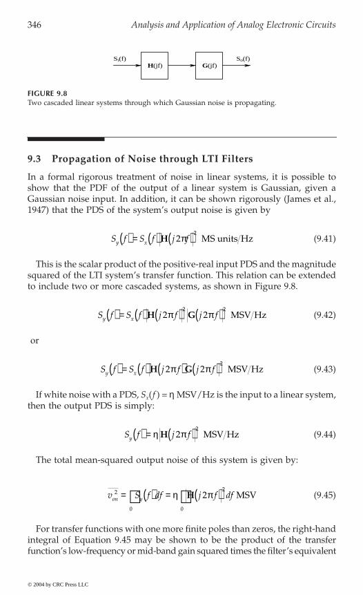
346 Analysis and Application of Analog Electronic Circuits
9.3 Propagation of Noise through LTI Filters
In a formal rigorous treatment of noise in linear systems, it is possible toshow that the PDF of the output of a linear system is Gaussian, given aGaussian noise input. In addition, it can be shown rigorously (James et al.,1947) that the PDS of the system’s output noise is given by
(9.41)
This is the scalar product of the positive-real input PDS and the magnitudesquared of the LTI system’s transfer function. This relation can be extendedto include two or more cascaded systems, as shown in Figure 9.8.
(9.42)
or
(9.43)
If white noise with a PDS, Sx(f ) = h MSV/Hz is the input to a linear system,then the output PDS is simply:
(9.44)
The total mean-squared output noise of this system is given by:
(9.45)
For transfer functions with one more finite poles than zeros, the right-handintegral of Equation 9.45 may be shown to be the product of the transferfunction’s low-frequency or mid-band gain squared times the filter’s equivalent
FIGURE 9.8Two cascaded linear systems through which Gaussian noise is propagating.
Si(f) So(f)H(jf) G(jf)
S f S f j fy x( ) = ( ) ( )H 22
p MS units Hz
S f S f j f j fy x( ) = ( ) ( ) ( )H G2 22 2
p p MSV Hz
S f S f j f j fy x( ) = ( ) ( ) ( )H G2 22
p p MSV Hz
S f j fy ( ) = ( )h pH 22 MSV Hz
v S f df j f dfon y2
0
2
0
2= ( ) = ( )• •
Ú Úh pH MSV
© 2004 by CRC Press LLC

Noise and the Design of Low-Noise Amplifiers for Biomedical Applications 347
Hertz noise bandwidth. Thus, the filter’s gain-squared bandwidth product isgiven by:
(9.46)
Gain2-bandwidth integrals have been evaluated for a number of transferfunctions using complex variable theory (James et al., 1947). Table 9.1 givesthe gain2-bandwidth integrals for five common transfer functions. Note thatthe equivalent noise bandwidths (in brackets in each case) are in Hertz, notradians/second. Also note the absence of any 2p factors in these expressions.Gain2-bandwidth integrals are used to estimate the total MS output noisefrom amplifiers with (approximate) white noise input sources and are thususeful in calculating output signal-to-noise ratios.
9.4 Noise Factor and Figure of Amplifiers
9.4.1 Broadband Noise Factor and Noise Figure of Amplifiers
An amplifier’s noise factor, F, is defined as the ratio of the mean-squaredsignal-to-noise ratio at the amplifier’s input to the MS signal-to-noise ratioat the amplifier’s output. Because a real amplifier is noisy and adds noiseto the signal as well as amplifying it, the output signal-to-noise ratio (SNRo)
TABLE 9.1
Gain2-Bandwidth Products for Some Common Filter Transfer Functions
Transfer Functiona Gain2 Bandwidthb Filter Type
1. Low pass; one real-pole
2. Low pass; two real poles
3. Low pass; underdamped quadratic
4. Underdamped quadratic band pass
5. Overdamped quadratic band pass
a H(s)b Hz
Ks
v
t + 1Kv
2 14t
ÊËÁ
ˆ¯
Ks s
v
t t1 21 1+( ) +( ) Kv2
1 2
14 t t+( )
Ê
ËÁ
ˆ
¯˜
Ks s
v
n n2 2 2 1w x w+ +
Kvn2
8w
xÊËÁ
ˆ¯
sK
s sv n
n n
2
2 12 2
x ww x w
( )+ +
Kv n2 xw( )
s Ks s
vtt t
1
1 21 1+( ) +( ) Kv2
2 2 1
14 1t t t+( )
Ê
ËÁ
ˆ
¯˜
GAIN BW2 2
0
2= ( )•
Ú H p fj df
© 2004 by CRC Press LLC
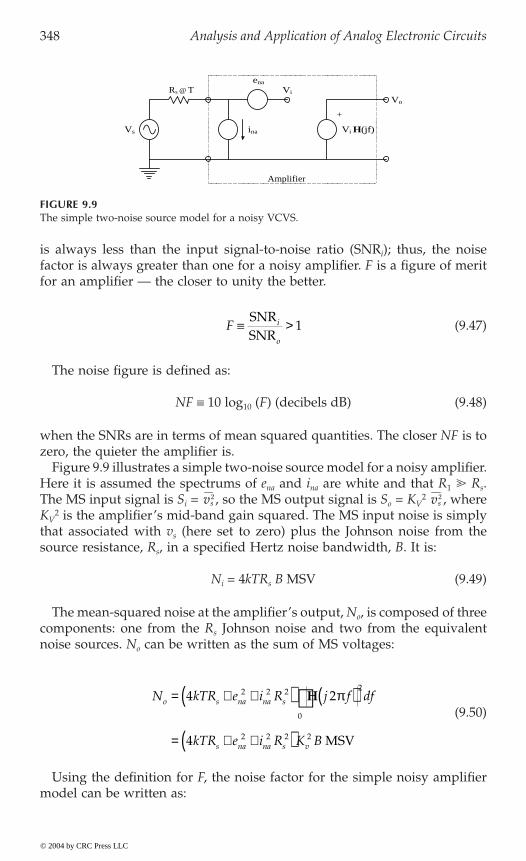
348 Analysis and Application of Analog Electronic Circuits
is always less than the input signal-to-noise ratio (SNRi); thus, the noisefactor is always greater than one for a noisy amplifier. F is a figure of meritfor an amplifier — the closer to unity the better.
(9.47)
The noise figure is defined as:
NF ∫ 10 log10 (F) (decibels dB) (9.48)
when the SNRs are in terms of mean squared quantities. The closer NF is tozero, the quieter the amplifier is.
Figure 9.9 illustrates a simple two-noise source model for a noisy amplifier.Here it is assumed the spectrums of ena and ina are white and that R1 Rs.The MS input signal is Si = , so the MS output signal is So = KV
2 , whereKV
2 is the amplifier’s mid-band gain squared. The MS input noise is simplythat associated with vs (here set to zero) plus the Johnson noise from thesource resistance, Rs, in a specified Hertz noise bandwidth, B. It is:
Ni = 4kTRs B MSV (9.49)
The mean-squared noise at the amplifier’s output, No, is composed of threecomponents: one from the Rs Johnson noise and two from the equivalentnoise sources. No can be written as the sum of MS voltages:
(9.50)
Using the definition for F, the noise factor for the simple noisy amplifiermodel can be written as:
FIGURE 9.9The simple two-noise source model for a noisy VCVS.
ena
Rs @ T
Amplifier
inaVs Vi H(jf)
Vo
Vi
+
F i
o
∫ >SNRSNR
1
vs2 vs
2
N kTR e i R j f df
kTR e i R K B
o s na na s
s na na s v
= + +( ) ( )
= + +( )
•
Ú4 2
4
2 2 2 2
0
2 2 2 2
H p
MSV
© 2004 by CRC Press LLC
Noise and the Design of Low-Noise Amplifiers for Biomedical Applications 349
(9.51)
Note that this expression for F contains no bandwidth terms; they cancelout. When the NF is given for an amplifier, Rs must be specified, as well asthe Hertz bandwidth, B, over which the noise is measured. The temperatureshould also be specified, although common practice usually sets T at 298 K(25∞C).
For practical amplifiers, NF and F are functions of frequency because ena andina s
at low frequencies due to the 1/f components in the equivalent input noisesources. F also increases at high frequencies — again, due to the high-fre-quency increases in ena and ina. Often, one is interested in the noise performanceof an amplifier in low or high frequencies in which the NF and F are notminimum. To examine the detailed noise performance of an amplifier at lowand high frequencies, use the spot noise figure (described next).
9.4.2 Spot Noise Factor and Figure
Spot noise measurements are made through a narrow band-pass filter inorder to evaluate an amplifier’s noise performance in a certain narrow fre-quency range, particularly where ena(f ) and ina(f ) are not constant, such as
for a commercial low-noise preamplifier with applications at audio frequen-cies. Note the area in Rs, f space at which the spot noise figure is a minimum.For best noise performance, the Thevenin resistance of the source, Rs, shouldlie in the range of minimum SNF and the input signal’s PDS should containmost of its energy in the range of frequencies at which the SNF is minimum.
A system for determining an amplifier’s spot noise figure is shown in
fier’s input. Note that the output resistance of the white noise source plussome external resistance must add up to Rs, the specified Thevenin equiva-lent input resistance. The system is used as follows: first, the band-pass filter(BPF) is set to the desired center frequency, fc, around which the amplifier’snoise performance is to be characterized. Then the white noise generator isset to eN = 0. Assume that the total mean squared noise at the system outputunder these conditions can be written as:
(9.52)
where ena(fc) is the value of ena at the center frequency; fc, BF is the equivalentnoise bandwidth of the BPF; and KV is the combined gain of the amplifierunder measurement at fc, the BPF at fc, and the postamplifier. KV can bewritten:
Fe i R
kTRna na s
s
= ++
14
2 2 2
N f kTR e f i f R K Bo c s na c na c s V F( ) = + ( ) + ( )[ ]4 2 2 2 2 MSV
© 2004 by CRC Press LLC
are functions of frequency (see Figure 9.6). For a given R , F tends to rise
the 1/f range. Figure 9.10 illustrates a set of spot noise figure (SNF) contours
Figure 9.11. An adjustable white noise voltage source is used at the ampli-

350 Analysis and Application of Analog Electronic Circuits
FIGURE 9.10Curves of constant spot noise figure (SNF) for a typical commercial low-noise amplifier. Notethe region in RS-f space at which the SNF is minimum (optimum).
FIGURE 9.11A test circuit for measuring an amplifier’s SNF.
10−2 10−1 1 10 102 103 104 105 106
f (Hz)
< 0.05 dB
0.1 dB
1 dB
10 dB
10 dB
1 dB20 dB
30 dB
40 dB
20 dB
103
104
105
106
108
109
10
102
RS (ohms)
107
Vi H(j2πf)ina
Von Vof
KF
BF
fc f00
KA
Vi
Differentialamplifier
Ideal BPFena
+
eN
True rmsvoltmeter
KAVof
Rs @ T
© 2004 by CRC Press LLC
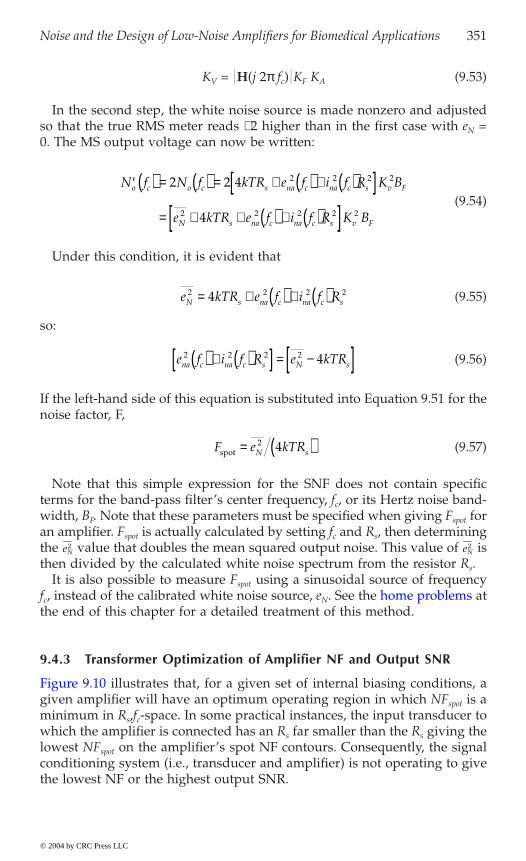
Noise and the Design of Low-Noise Amplifiers for Biomedical Applications 351
KV = H(j 2p fc) KF KA (9.53)
In the second step, the white noise source is made nonzero and adjustedso that the true RMS meter reads ÷2 higher than in the first case with eN =0. The MS output voltage can now be written:
(9.54)
Under this condition, it is evident that
(9.55)
so:
(9.56)
If the left-hand side of this equation is substituted into Equation 9.51 for thenoise factor, F,
(9.57)
Note that this simple expression for the SNF does not contain specificterms for the band-pass filter’s center frequency, fc, or its Hertz noise band-width, BF. Note that these parameters must be specified when giving Fspot foran amplifier. Fspot is actually calculated by setting fc and Rs, then determiningthe value that doubles the mean squared output noise. This value of isthen divided by the calculated white noise spectrum from the resistor Rs.
It is also possible to measure Fspot using a sinusoidal source of frequencyc N
the end of this chapter for a detailed treatment of this method.
9.4.3 Transformer Optimization of Amplifier NF and Output SNR
given amplifier will have an optimum operating region in which NFspot is aminimum in Rs,fc-space. In some practical instances, the input transducer towhich the amplifier is connected has an Rs far smaller than the Rs giving thelowest NFspot on the amplifier’s spot NF contours. Consequently, the signalconditioning system (i.e., transducer and amplifier) is not operating to givethe lowest NF or the highest output SNR.
¢ ( ) = ( ) = + ( ) + ( )[ ]= + + ( ) + ( )[ ]
N f N f kTR e f i f R K B
e kTR e f i f R K B
o c o c s na c na c s v F
N s na c na c s v F
2 2 4
4
2 2 2 2
2 2 2 2 2
e kTR e f i f RN s na c na c s2 2 2 24= + ( ) + ( )
e f i f R e kTRna c na c s N s2 2 2 2 4( ) + ( )[ ] = -[ ]
F e kTRN sspot = ( )2 4
eN2 eN
2
© 2004 by CRC Press LLC
Figure 9.10 illustrates that, for a given set of internal biasing conditions, a
f , instead of the calibrated white noise source, e . See the home problems at
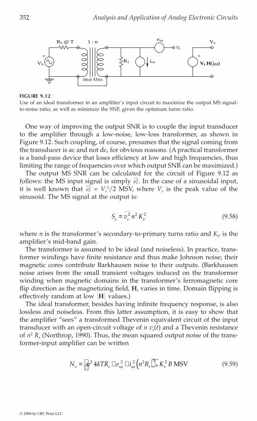
352 Analysis and Application of Analog Electronic Circuits
One way of improving the output SNR is to couple the input transducerto the amplifier through a low-noise, low-loss transformer, as shown inFigure 9.12. Such coupling, of course, presumes that the signal coming fromthe transducer is ac and not dc, for obvious reasons. (A practical transformeris a band-pass device that loses efficiency at low and high frequencies, thuslimiting the range of frequencies over which output SNR can be maximized.)
The output MS SNR can be calculated for the circuit of Figure 9.12 asfollows: the MS input signal is simply . In the case of a sinusoidal input,it is well known that = Vs
2/2 MSV, where Vs is the peak value of thesinusoid. The MS signal at the output is:
(9.58)
where n is the transformer’s secondary-to-primary turns ratio and KV is theamplifier’s mid-band gain.
The transformer is assumed to be ideal (and noiseless). In practice, trans-former windings have finite resistance and thus make Johnson noise; theirmagnetic cores contribute Barkhausen noise to their outputs. (Barkhausennoise arises from the small transient voltages induced on the transformerwinding when magnetic domains in the transformer’s ferromagnetic coreflip direction as the magnetizing field, H, varies in time. Domain flipping iseffectively random at low H values.)
The ideal transformer, besides having infinite frequency response, is alsolossless and noiseless. From this latter assumption, it is easy to show thatthe amplifier “sees” a transformed Thevenin equivalent circuit of the inputtransducer with an open-circuit voltage of n vs(t) and a Thevenin resistanceof n2 Rs (Northrop, 1990). Thus, the mean squared output noise of the trans-former-input amplifier can be written
(9.59)
FIGURE 9.12Use of an ideal transformer in an amplifier’s input circuit to maximize the output MS signal-to-noise ratio, as well as minimize the SNF, given the optimum turns ratio.
RS @ T
Vi H(jω)
Vo
ina
ena
R1
+
1 : n
Ideal Xfmr.
+
VS
Vi
vs2
vs2
S v n Ko s v= 2 2 2
N n kTR e i n R K Bo s na na s v= + + ( )ÈÎÍ
˘˚
2 2 2 2 2 24 MSV
© 2004 by CRC Press LLC

Noise and the Design of Low-Noise Amplifiers for Biomedical Applications 353
and the output SNR is:
(9.60)
The SNRo clearly has a maximum with respect to the turns ratio, n. (It canbe shown that F is minimum when n = no, so SNRo is maximum (Northrop,1997). If the denominator of Equation 9.60 is differentiated with respect ton2 and set equal to zero, an optimum turns ratio, no, exists that will maximizeSNRo. no is given by:
(9.61)
If the noiseless (ideal) transformer is given the turns ratio of no, then it iseasy to show that the maximum output SNR is given by:
(9.62)
The general effect of transformer SNR maximization on the system’s noisefigure contours is to shift the locus of minimum NFspot to a lower range ofRs; no obvious shift occurs along the fc axis. Also, the minimum NFspot ishigher with a real transformer because a practical transformer is noisy, asdiscussed earlier. As a rule of thumb, using a transformer to improve outputSNR and reduce NFspot is justified if (ena
2 + ina2 Rs
2) > 20 ena ina Rs in the rangeof frequencies of interest (Northrop, 1990).
9.5 Cascaded Noisy Amplifiers
9.5.1 Introduction
To achieve the required high gain required for certain biomedical signalconditioning applications, it is often necessary to place several IC gain stagesin series. A natural question to ask is whether all the component IC gainstages need to be low noise in the low-noise amplifier design. The good newsis that as long as the headstage (input, or first stage) is low noise and has again magnitude of ≥10, the remaining gain stages do not need to be low noisein design. The headstage’s noise sets the noise performance of the completesignal conditioning amplifier.
SNRos
s na na s
v BkTR e n i n R
=+ +
2
2 2 2 2 24
n e i Ro na na s= ( )
SNROs
s na na s
v BkTR e i Rmax =
+
2
4 2
© 2004 by CRC Press LLC

354 Analysis and Application of Analog Electronic Circuits
9.5.2 The SNR of Cascaded Noisy Amplifiers
Figure 9.13 illustrates three cascaded amplifier stages. The amplifier’s overallgain is KV = KV1 KV2 KV3. The first stage has a white, short-circuit voltage,root power spectrum of ena1 RMSV/÷Hz and an input current noise rootpower spectrum of ina1 RMS V/÷Hz. The other two stages have voltage noisesof ena2 and ena3, respectively, and zero current noises. (It can be assumed thatthe current noises are zero because the output resistance of the previousstages is assumed to be very low, so that ina2 Ro1 ena2, and ina3 Ro2 ena3.)Assume a sinusoidal input signal, vs(t) = Vs sin(2pft); thus, the MS inputvoltage is Vs
2/2. The MS output voltage is simply = (Vs2/2)(KV1KV2KV3)2.
The total MS noise output voltage is the sum of the MS noise componentsfrom the noise sources: von
2 = [ena12 + ina1
2iRs2](KV1KV2KV3)2 + ena2
2 (KV2KV3)2 +ena3
2 (KV3)2. The output MS signal-to-noise ratio can now be examined for thethree-stage amplifier:
Ø
(9.63)
Thus, the SNRo of the three-stage cascaded amplifier is set by the headstagealone, as long as the headstage gain KV1 > 10.
What if the headstage is of necessity a source or emitter follower withnear-unity gain? If the preceding equation is examined, it can be seen thatit reduces to a lower value for KV1 Æ 1, e.g.,
(9.64)
FIGURE 9.13Three cascaded noisy amplifiers.
RS @ T ena1V1
ena2V2
ena3V3 Vo
KV1 KV2 KV3
vs
+
vos2
SNRos V V V
na na s V V V na V V na V
V K K K
e i R K K K e K K e K B=
( ) ( )+[ ]( ) + ( ) + ( )
21 2 3
2
12
12 2
1 2 3
2
22
2 3
2
32
3
2
2
SNRos
na na s na V na V V
s
na na s
V B
e i R e K e K K
V B
e i R=
( )+[ ] + + ( )
@( )
+[ ]2
12
12 2
22
12
32
1 2
2
2
12
12 2
2 2
SNRos
na na s na na V
V B
e i R e e K@
( )+[ ] + + ( )
2
12
12 2
22
32
2
2
2
© 2004 by CRC Press LLC
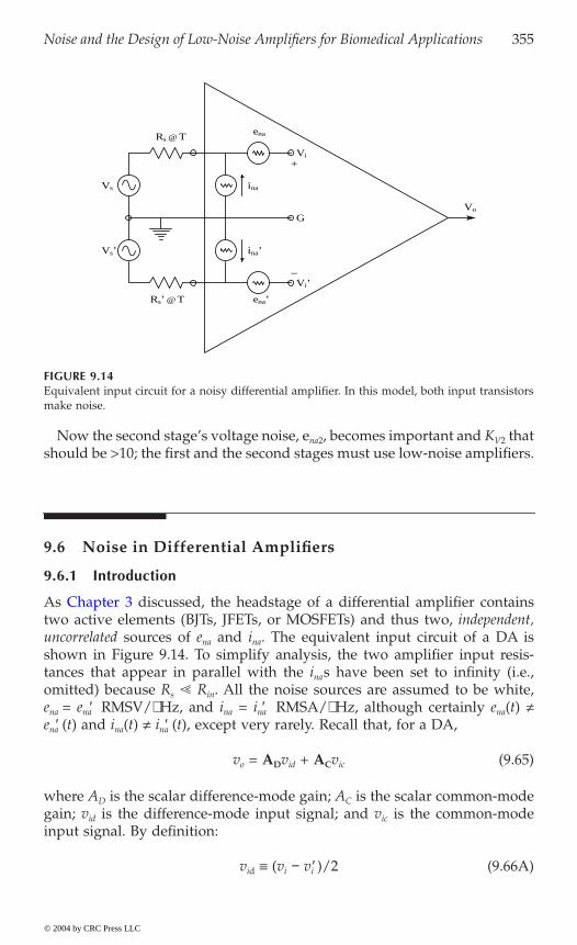
Noise and the Design of Low-Noise Amplifiers for Biomedical Applications 355
Now the second stage’s voltage noise, ena2, becomes important and KV2 thatshould be >10; the first and the second stages must use low-noise amplifiers.
9.6 Noise in Differential Amplifiers
9.6.1 Introduction
two active elements (BJTs, JFETs, or MOSFETs) and thus two, independent,uncorrelated sources of ena and ina. The equivalent input circuit of a DA isshown in Figure 9.14. To simplify analysis, the two amplifier input resis-tances that appear in parallel with the inas have been set to infinity (i.e.,omitted) because Rs Rin. All the noise sources are assumed to be white,ena = ena¢ RMSV/÷Hz, and ina = ina¢ RMSA/÷Hz, although certainly ena(t) πena¢ (t) and ina(t) π ina¢ (t), except very rarely. Recall that, for a DA,
vo = ADvid + ACvic (9.65)
where AD is the scalar difference-mode gain; AC is the scalar common-modegain; vid is the difference-mode input signal; and vic is the common-modeinput signal. By definition:
vid ∫ (vi - vi¢ )/2 (9.66A)
FIGURE 9.14Equivalent input circuit for a noisy differential amplifier. In this model, both input transistorsmake noise.
ena
ena’
ina’
ina
Vo
Rs @ T
Rs’ @ T
Vs
Vs’
Vi
Vi’
+
−
G
© 2004 by CRC Press LLC
As Chapter 3 discussed, the headstage of a differential amplifier contains

356 Analysis and Application of Analog Electronic Circuits
vic ∫ (vi + vi¢ )/2 (9.66B)
Also recall that the common-mode rejection ratio for the simple DA couldbe expressed as:
CMRR ∫ AD/AC (9.67)
Under normal operating conditions, AD AC and CMRR 1.
9.6.2 Calculation of the SNRO of the DA
uncorrelated noise sources. Thus the total noise PDS at the vi node can bewritten:
Sni = ena2 + ina
2Rs2 + 4kTRs MSV/Hz (9.68)
Similarly, the total noise PDS at the vi¢ node is:
Sni¢ = ena¢ 2 + ina¢ 2 Rs2 + 4kTRs MSV/Hz (9.69)
To find the MS SNRo of the noisy DA, assume that the input signal is pureDM. Thus vic = 0, vid = vs, and = AD
2 MSV. To find the MS noise output,set vs = vs¢ = 0 and consider that the six noise sources add in quadrature (inan MS sense). First, note that in the time domain:
vi(t) = ena(t) + ina(t)Rs + enrs(t) V (9.70)
and
vi¢(t) = ena¢ (t) + ina¢ (t)Rs¢+ enrs¢ (t) V (9.71)
Now expand and square Equation 9.65 for the amplifier output:
When the expressions for vi(t) and vi¢(t) from Equation 9.70 and Equation9.71 are substituted into Equation 9.72 and the expectation or mean is taken,cross terms between vi and vi¢ vanish because of statistical independence andno correlation. Also, the means of self-cross terms such as ena¢(ina¢Rs¢) alsovanish for the same reasons. Recall that because the DA is symmetrical, ena =ena¢ RMSV/÷Hz, ina = ina¢ RMSA/÷Hz and Rs = Rs¢. After some algebra thatwill not be reproduced here, the MS output noise is given by:
vos2 vs
2
v t Av v v v
A Av v v v
Av v v
von Di i i i
D Ci i i i
Ci i i
i2 2
2 22
222
42
2 224
( ) = - ¢ + ¢È
ÎÍ
˘
˚˙ + - ¢È
Î͢˚
+ ¢ÈÎÍ
˘˚
+ + ¢ + ¢È
ÎÍ
˘
˚˙
(9.72)
© 2004 by CRC Press LLC
Referring to Figure 9.14, the DA noise model circuit has six independent,
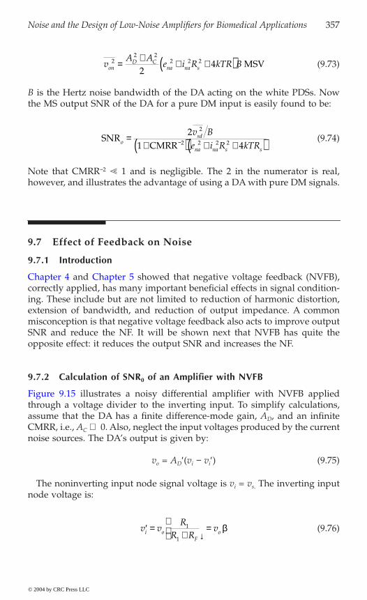
Noise and the Design of Low-Noise Amplifiers for Biomedical Applications 357
(9.73)
B is the Hertz noise bandwidth of the DA acting on the white PDSs. Nowthe MS output SNR of the DA for a pure DM input is easily found to be:
(9.74)
Note that CMRR-2 1 and is negligible. The 2 in the numerator is real,however, and illustrates the advantage of using a DA with pure DM signals.
9.7 Effect of Feedback on Noise
9.7.1 Introduction
correctly applied, has many important beneficial effects in signal condition-ing. These include but are not limited to reduction of harmonic distortion,extension of bandwidth, and reduction of output impedance. A commonmisconception is that negative voltage feedback also acts to improve outputSNR and reduce the NF. It will be shown next that NVFB has quite theopposite effect: it reduces the output SNR and increases the NF.
9.7.2 Calculation of SNR0 of an Amplifier with NVFB
through a voltage divider to the inverting input. To simplify calculations,assume that the DA has a finite difference-mode gain, AD, and an infiniteCMRR, i.e., AC Æ 0. Also, neglect the input voltages produced by the currentnoise sources. The DA’s output is given by:
vo = AD¢(vi - vi¢) (9.75)
The noninverting input node signal voltage is vi = vs. The inverting inputnode voltage is:
(9.76)
vA A
e i R kTR BonD C
na na s2
2 22 2 2
24=
++ +( ) MSV
SNRCMRRo
sd
na na s s
v Be i R kTR
=+( ) + +( )-
21 4
2
2 2 2 2
¢ =+
ÊËÁ
ˆ¯
=v vR
R Rvi o
Fo
1
1
b
© 2004 by CRC Press LLC
Figure 9.15 illustrates a noisy differential amplifier with NVFB applied
Chapter 4 and Chapter 5 showed that negative voltage feedback (NVFB),
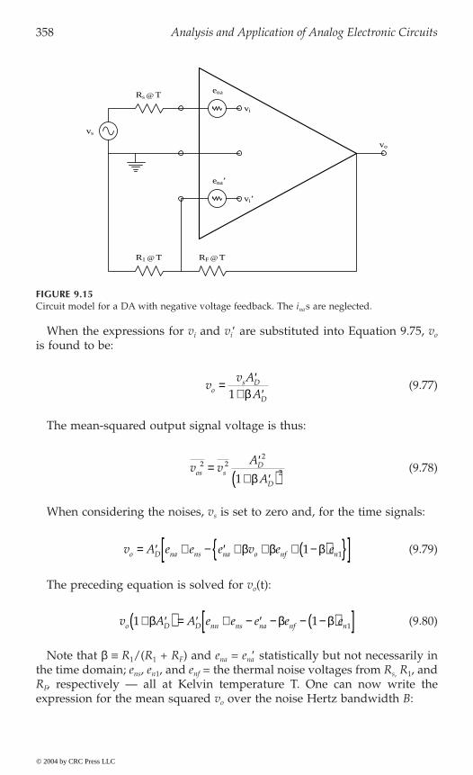
358 Analysis and Application of Analog Electronic Circuits
When the expressions for vi and vi¢ are substituted into Equation 9.75, vo
is found to be:
(9.77)
The mean-squared output signal voltage is thus:
(9.78)
When considering the noises, vs is set to zero and, for the time signals:
(9.79)
The preceding equation is solved for vo(t):
(9.80)
Note that b ∫ R1/(R1 + RF) and ena = ena¢ statistically but not necessarily inthe time domain; ens, en1, and enf = the thermal noise voltages from Rs, R1, andRF, respectively — all at Kelvin temperature T. One can now write theexpression for the mean squared vo over the noise Hertz bandwidth B:
FIGURE 9.15Circuit model for a DA with negative voltage feedback. The ina s are neglected.
ena’
ena
vi
vi’
Rs @ T
vs
R1 @ T RF @ T
vo
vv A
Aos D
D
= ¢+ ¢1 b
v vA
Aos s
D
D
2 22
21
= ¢+ ¢( )b
v A e e e v e eo D na ns na o nf n= ¢ + - ¢ + + + -( ) [ ]b b b1 1
v A A e e e e eo D D nn ns na nf n1 1 1+ ¢( ) = ¢ + - ¢ - - -( )[ ]b b b
© 2004 by CRC Press LLC
Noise and the Design of Low-Noise Amplifiers for Biomedical Applications 359
(9.81)
The MS signal-to-noise ratio of the feedback amplifier is found by takingthe ratio of Equation 9.78 to Equation 9.81:
(9.82)
It is left as an exercise for the reader to show that, in the absence of feedback(no feedback resistors at all), the output SNR is:
(9.83)
Note that the presence of the feedback voltage divider resistors adds noiseto the output and gives a lower SNRo. Contemplate the effect of applyingfeedback through a purely capacitive voltage divider. Capacitors do notgenerate thermal noise.
9.8 Examples of Noise-Limited Resolution of Certain Signal Conditioning Systems
9.8.1 Introduction
In following examples, assume that the stationary sources of noise (resistorthermal noise, amplifier ena and ina) are statistically independent, are uncor-related, have white spectra in the range of frequencies of interest, and areadded in the MS sense as PDSs are. Aside from their short-circuit inputvoltage noise, ena, the op amps are assumed to be ideal.
9.8.2 Calculation of the Minimum Resolvable AC Input Voltage to a Noisy Op Amp
input. Assume that ina RF ena and thus ina produces negligible noise at theamplifier output and is deleted from the model. Only amplifier ena andresistor Johnson noise contribute to the amplifier’s noise output. The mean-squared signal output is given by:
vA
Ae kTR kTR kTR Bon
D
D
na s F2
2
22 2 2
11
2 4 4 1 4= ¢+ ¢( )
+ + + -( )[ ]bb b
SNRos
na S F
v B
e kT R R R=
+ + + -( )[ ]2
2 2 212 4 1b b
SNRos
na s
v Be kTR
=+
2
22 4
© 2004 by CRC Press LLC
Figure 9.16 illustrates a simple inverting op amp circuit with a sinusoidal

360 Analysis and Application of Analog Electronic Circuits
(9.84)
The noise voltages in this circuit are all conditioned by different gains: en1
is the thermal noise from R1; it is conditioned by the same gain as vs, i.e.,(–RF/R1). Because the summing junction is at 0 V due to the ideal op ampassumption, the thermal noise in RF, enf, is seen at the output as simply enf
(a gain of unity). Again, the gain for ena is found by assuming vi¢ = 0. Thevoltage at the R1–RF node thus must be ena; therefore, the voltage dividerratio gives vo = ena (1 + RF/R1). Note that these three gains are derivedassuming ena, enf, and en1 are voltages varying in time. When the MS noise atthe output is examined, the gains must be squared.
Using the principles described previously, the total MS noise at the op ampoutput is:
Note that the equivalent noise bandwidth, B, must be used to effectivelyintegrate the white output PDS, giving MSV. The MS SNRo of the amplifieris thus:
(9.86)
Ø
(9.87)
Ø
FIGURE 9.16A simple inverting op amp circuit with a sinusoidal voltage input. White thermal noise isassumed to come from the two resistors and also from the op amp’s ena.
+
VS
R1 @ T
RF @ T
ena
OAVo
vi’
vi
v V R Ros S F2 2
1
22= ( ) -( )
v kTR R R kTR e R R Bon F F na F2
1 1
2 21 2
4 4 1= -( ) + + +( )
SNRoS F
F F na F F
V R R
kTR R R kTR e R R R R B=
( ) -( )-( ) + + + + ( )[ ]
21
2
1 1
2 21 1
2
2
4 4 1 2
SNRoS
F F na F F F
V B
kTR kTR R R e R R R R R R=
( )+ ( ) + + + ( )[ ]( )
2
1 1
2 21 1
2
1
2
2
4 4 1 2
© 2004 by CRC Press LLC
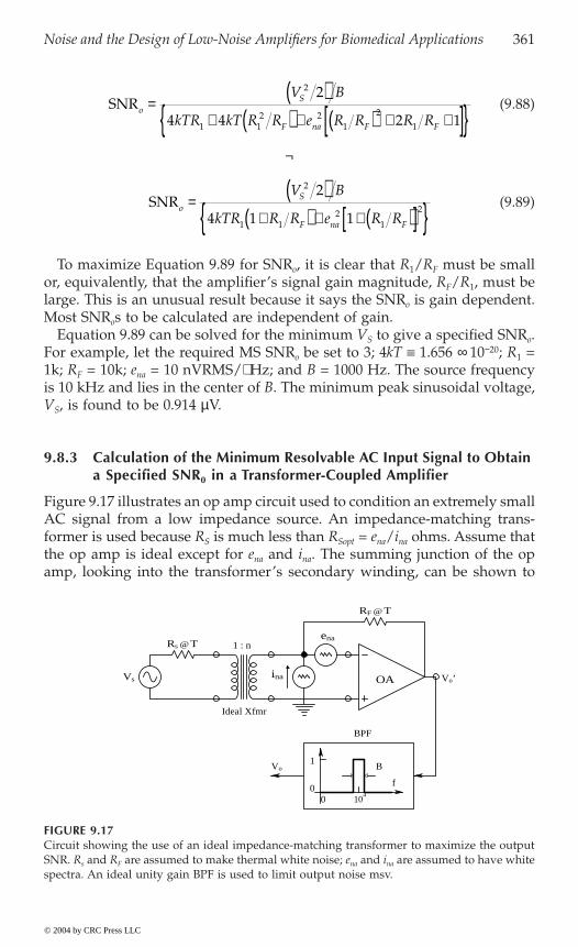
Noise and the Design of Low-Noise Amplifiers for Biomedical Applications 361
(9.88)
Ø
(9.89)
To maximize Equation 9.89 for SNRo, it is clear that R1/RF must be smallor, equivalently, that the amplifier’s signal gain magnitude, RF/R1, must belarge. This is an unusual result because it says the SNRo is gain dependent.Most SNRos to be calculated are independent of gain.
Equation 9.89 can be solved for the minimum VS to give a specified SNRo.For example, let the required MS SNRo be set to 3; 4kT ∫ 1.656 ¥ 10-20; R1 =1k; RF = 10k; ena = 10 nVRMS/÷Hz; and B = 1000 Hz. The source frequencyis 10 kHz and lies in the center of B. The minimum peak sinusoidal voltage,VS, is found to be 0.914 mV.
9.8.3 Calculation of the Minimum Resolvable AC Input Signal to Obtain a Specified SNR0 in a Transformer-Coupled Amplifier
Figure 9.17 illustrates an op amp circuit used to condition an extremely smallAC signal from a low impedance source. An impedance-matching trans-former is used because RS is much less than RSopt = ena/ina ohms. Assume thatthe op amp is ideal except for ena and ina. The summing junction of the opamp, looking into the transformer’s secondary winding, can be shown to
FIGURE 9.17Circuit showing the use of an ideal impedance-matching transformer to maximize the outputSNR. Rs and RF are assumed to make thermal white noise; ena and ina are assumed to have whitespectra. An ideal unity gain BPF is used to limit output noise msv.
SNRoS
F na F F
V B
kTR kT R R e R R R R=
( )+ ( ) + ( ) + +[ ]
2
1 12 2
1
2
1
2
4 4 2 1
SNRoS
F na F
V B
kTR R R e R R=
( )+( ) + + ( )[ ]
2
1 12
1
2
2
4 1 1
1 : n
B
Vo’
Ideal Xfmr
Rs @ Tena
RF @ T
BPF
Vo
f
00
104
OA
1
inaVs
© 2004 by CRC Press LLC
362 Analysis and Application of Analog Electronic Circuits
“see” an input Thevenin equivalent circuit with an open-circuit voltage ofn vs and a Thevenin resistance of n2 RS (Northrop, 1990). Thus, the outputvoltage due to the signal is vos = n vs [-RF/n2 RS] and the MS signal is:
(9.90)
The op amp’s output is filtered by an (ideal) band-pass filter with peakgain = 1 and noise bandwidth, B, Hertz centered at fs, the signal frequency.The filter is used to restrict the noise power at the output while passing thesignal.
Finding the output noise is somewhat more complicated. The gain for ens,the thermal noise from RS, is the same as for vs, i.e., [RF/n2RS ]. The gain forinf, the thermal noise from RF, is 1. The gain (transresistance) for ina is RF. Thegain for ena can be shown to be [1 + RF/(n2RS)] (Northrop, 1990). By usingthe superposition of mean-squared voltages, the total noise MS output volt-age can be written:
(9.91)
The output SNR is easily written:
(9.92)
The denominator of Equation 9.92 has a minimum for some non-negativetransformer turns ratio, no; thus, SNRo is maximum for n = no. To find no,differentiate the denominator with respect to n2 and set the derivative equalto zero, then solve for no.
(9.93)
Ø
(9.94)
Ø
(9.95)
v v R nRos s F S2 2 2
= [ ] MSV
v e R n R i R kTR kTR R nR Bon na F S na F F S F S2 2 2
22 2 2
1 4 4= + ( )[ ] + + + [ ]ÏÌÓ¸˛
MSV
SNRos
S na S F na S F S F
v B
kTR e nR R n i R n kTR nR R=
+ +[ ] + + [ ]2
2 2 2 2 2 24 1 4
0 4 1 422 2 2 2 2 2
= + +[ ] + + [ ] ddn
kTR e nR R n i R n kTR nR RS na S F na S F S F
0 1 42 2 2 4 2 2 2= [ ] + -[ ] + + [ ]e R R e n i R kTR R Rna S F na o na S F S F
ne R
e R kTR io
na S
na F F na
=( ) + + 2 2 24
14
© 2004 by CRC Press LLC

Noise and the Design of Low-Noise Amplifiers for Biomedical Applications 363
Now calculate the turns ratio, no, that will maximize SNRo. Define theparameters: ena = 3 nVRMS/÷Hz (white); ina = 0.4 pARMS/÷Hz (white); RF
= 104 ohms; RS = 10 ohms; 4kT = 1.656 ¥ 10-20; and B = 103 Hz. Using Equation9.95, no = 14.73 (the secondary-to-primary ratio does not need to be aninteger). Using no = 14.73, the desirable MS SNRo = 3; substitute the precedingnumerical values into Equation 9.92 and solve for the vs RMS required: vs =28.3 nVRMS. If no transformer is used (equivalent to n = 1 in Equation 9.92),vs = 166 nVRMS is needed for the MS SNRo = 3.
9.8.4 The Effect of Capacitance Neutralization on the SNR0 of an Electrometer Amplifier Used for Glass Micropipette Intracellular Recording
Measurement of the transmembrane potential of neurons, muscle cells,and other cells is generally done with hollow glass micropipettes filled witha conductive electrolyte solution such as 3M KCl (Lavallée et al., 1969). Inorder for the glass micropipette electrode to penetrate the cell membrane,the tips are drawn down to diameters of the order of 0.5 mm; the smalldiameter tips give micropipettes their high series resistance, Rm. Figure 9.18illustrates a simplified lumped-parameter model for a glass microelectrodewith its tip in a cell. Rm is on the order of 50 to 500 megohms. CT is theequivalent lumped shunt capacitance across the electrode’s tip glass; it is onthe order of single picofarads.
The electrometer amplifier (EA) used to condition signals recorded intra-cellularly with a glass micropipette microelectrode is direct-coupled, has alow noninverting gain between 2 and 5, and is characterized by its extremelyhigh input impedance (approximately 1015 W) and very low dc bias current(approximately 100 fA). The latter two properties are necessary because the
FIGURE 9.18Circuit used to model noise in a capacity-neutralized electrometer amplifier supplied by a glassmicropipette electrode. Only white thermal noise from the microelectrode’s internal resistanceis considered along with the white noises, ena and ina.
Rµ @ Tena
Vb ina
CN
RF
R1
Cµ + Cin
V1Vi
Vi’VoEOA
+
© 2004 by CRC Press LLC
364 Analysis and Application of Analog Electronic Circuits
Thevenin source resistance of the microelectrode is so high and, for practicalreasons, negligible dc bias current should flow through it to prevent ion driftat the tip. For all practical purposes, the EA can be treated as a noisy butotherwise ideal voltage amplifier. The so-called capacitive neutralization isaccomplished by positive feedback applied though the variable capacitor, CN.
The transfer functions for the biosignal, Vb, and the amplifier noises, ena
and ina, will now be found. Assume the EA’s gain is +3. To do this, first writethe node equation for the v1 node in terms of the Laplace variable, s:
V1 [Gm + sCT + sCN] - 3V1 sCN = Vb Gm (9.96)
Equation 9.96 can be solved for V1:
(9.97)
Thus,
(9.98)
Note that, in this simple case, when CN is made CT/2, the amplifier’s timeconstant Æ 0, thus the break frequency fb = 1/2pt Æ • and Vo = 3Vb.
Now consider the transfer function for the EA’s current noise, ina:
V1 [Gm + s (CT + CN)] - 3V1CN = ina (9.99)
This node equation leads to the transfer impedance:
(9.100)
Now find the transfer function for ena. Again, write a node equation:
V1¢[Gm + s (CT + CN)] - 3V1CN = 0 (9.101)
Note that when V1¢ = V1 - ena is substituted into Equation 9.101, it is possibleto solve for the transfer function:
(9.102)
In summary, when CN = CT/2, the amplifier is neutralized and the noisegains are:
VV
sR C Cb
T N1 1 2
=+ -( )m
VV
sR C Cob
T N
=+ -( )
31 2m
Vi
R
sR C Co
na T N
=+ -( )
3
1 2m
m
Ve
sR C C
sR C Co
na
T N
T N
=+ +( )[ ]
+ -( )3 1
1 2m
m
© 2004 by CRC Press LLC

Noise and the Design of Low-Noise Amplifiers for Biomedical Applications 365
Vo = 3 enm (enm is the thermal noise from Rm.) (9.103A)
Vo = 3Rm ina (9.103B)
Vo = ena 3[1 + sRm(3CT/2)] (9.103C)
The total MS noise output of the C-neut. amp is found by superpositionof the three mean-squared noise components:
(9.104A)
Ø
(9.104B)
The fourth term in Equation 9.104B represents excess noise introduced bythe positive feedback through the neutralizing capacitor. B is the Hertz noisebandwidth of the unity-gain ideal low-pass filter used to limit the outputnoise. Calculating the RMS output noise of the neutralized amplifier: theparameters are amplifier gain = 3; ena = 35 nV RMS/÷Hz (white); ina = 1.1 ¥10-16 A RMS/÷Hz (white); Rm = 108 W; CT = 5 pF; 4kT = 1.656 ¥ 10-20; and B =5E3 Hz. When substituted into Equation 9.104B, von = 2.915 ¥ 10-4 V RMS,or about 0.3 mV RMS. The corner frequency for the output noise due to ena
under conditions of neutralization is:
(9.105)
Numerically, this is 212 Hz.Finally, the SNRo of the neutralized amplifier can be written:
(9.106)
As a final exercise, find the RMS Vb required to give an MS SNRo = 9.Substituting the preceding numerical values, Vb = 8.75 ¥ 10-4 V RMS.
9.8.5 Calculation of the Smallest Resolvable DDDDR/R in a Wheatstone Bridge Determined by Noise
9.8.5.1 Introduction
The Wheatstone bridge is typically associated with the precision measure-ment of resistance. However, this simple ubiquitous circuit is used as an
N kTR R i B e j fR C dfo na na T
B
= ( ) + + + ( )Ú9 4 9 9 1 2 3 22 2 2 2
0
m m mp MSV
N kTR R i e B e B R Co na na na T= ( ) + + + ( ) ( )[ ]4 9 9 3 2 3 22 2 2 2 3 2
m m mp MSV
f R Cc T= ( )[ ]1 2 3 2p m Hz
SNRob
na na na T
V
kTR R i e B e B R C=
( ) + + + ( ) ( )[ ]2
2 2 2 2 3 24 3 2 3 2m m mp
© 2004 by CRC Press LLC
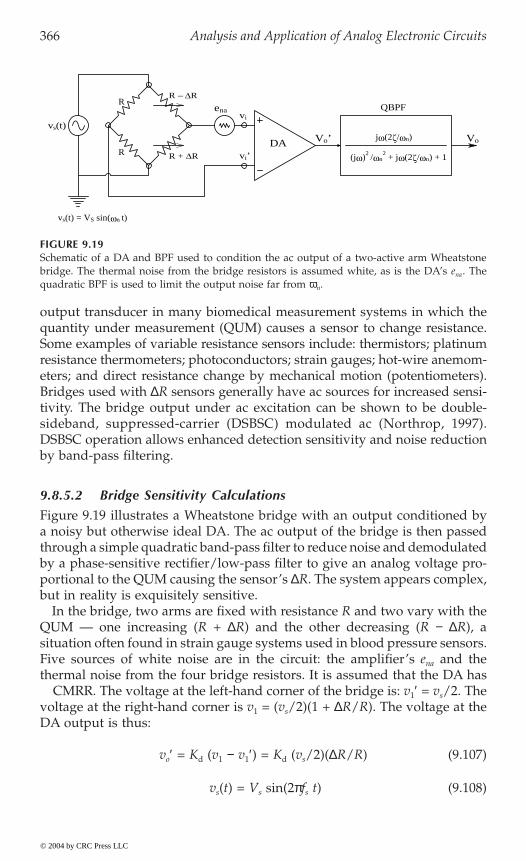
366 Analysis and Application of Analog Electronic Circuits
output transducer in many biomedical measurement systems in which thequantity under measurement (QUM) causes a sensor to change resistance.Some examples of variable resistance sensors include: thermistors; platinumresistance thermometers; photoconductors; strain gauges; hot-wire anemom-eters; and direct resistance change by mechanical motion (potentiometers).Bridges used with DR sensors generally have ac sources for increased sensi-tivity. The bridge output under ac excitation can be shown to be double-sideband, suppressed-carrier (DSBSC) modulated ac (Northrop, 1997).DSBSC operation allows enhanced detection sensitivity and noise reductionby band-pass filtering.
9.8.5.2 Bridge Sensitivity Calculations
Figure 9.19 illustrates a Wheatstone bridge with an output conditioned bya noisy but otherwise ideal DA. The ac output of the bridge is then passedthrough a simple quadratic band-pass filter to reduce noise and demodulatedby a phase-sensitive rectifier/low-pass filter to give an analog voltage pro-portional to the QUM causing the sensor’s DR. The system appears complex,but in reality is exquisitely sensitive.
In the bridge, two arms are fixed with resistance R and two vary with theQUM — one increasing (R + DR) and the other decreasing (R - DR), asituation often found in strain gauge systems used in blood pressure sensors.Five sources of white noise are in the circuit: the amplifier’s ena and thethermal noise from the four bridge resistors. It is assumed that the DA has• CMRR. The voltage at the left-hand corner of the bridge is: v1¢ = vs/2. Thevoltage at the right-hand corner is v1 = (vs/2)(1 + DR/R). The voltage at theDA output is thus:
vo¢ = Kd (v1 - v1¢) = Kd (vs/2)(DR/R) (9.107)
vs(t) = Vs sin(2pfs t) (9.108)
FIGURE 9.19Schematic of a DA and BPF used to condition the ac output of a two-active arm Wheatstonebridge. The thermal noise from the bridge resistors is assumed white, as is the DA’s ena. Thequadratic BPF is used to limit the output noise far from wn.
VoVo’
enaR
R
R − ∆R
DA(jω)
2/ωn
2+ jω(2ζ/ωn) + 1R + ∆R
jω(2ζ/ωn)
vi’
vi
QBPF
vs(t) = VS sin(ωn t)
vs(t)
© 2004 by CRC Press LLC

Noise and the Design of Low-Noise Amplifiers for Biomedical Applications 367
vo¢ passes through the BPF with unity gain, so the MS output due to DR/Ris:
(9.109)
9.8.5.3 Bridge SNRo
The noise power density spectrum at the DA output is found by superpo-sition of PDSs:
Sno¢ (f ) = [4kTR/2 + 4kTR/2 + ena2 ] Kd
2 MSV/Hz (white) (9.110)
The gain2-bandwith integral for the unity-gain quadratic BPF with Q =1/2x has been shown to be (2pfs/2Q) Hz. Thus, the MS noise at the filteroutput is:
(9.111)
and the SNRo is:
(9.112)
Equation 9.112 can be used to find the numerical DR/R required to give aSNRo = 1. Let fs = 1 kHz; 4kT = 1.656 ¥ 10-20; Q = 2; ena = 10 nVRMS/÷Hz;R = 400 W; Kd = 103; and Vs = 5 Vpk. From these values, DR/R is found tobe 2.315 ¥ 10-7 and DR = 0.2315 mW. Also, the DA output is 0.579 mVpk.
If a sensor’s sensitivity (e.g., for a blood pressure sensor), and how manymmHg cause a given DR/R are known, it is easy to find the noise-limitedDP from Equation 9.112.
9.8.6 Calculation of the SNR Improvement Using a Lock-In Amplifier
A lock-in amplifier (LIA) is used to measure coherent signals, generally ataudio frequencies, that are “buried in noise.” More precisely, the input signal-to-noise ratio is very low, often as low as –60 dB. There are two basicarchitectures used for LIAs. One uses an analog multiplier for signal detec-
second LIA architecture, shown in Figure 9.20(B), uses a synchronous recti-fier followed by a low-pass filter to measure the amplitude of a coherentsignal of constant frequency that is present in an overwhelming amount ofnoise.
v V K R Ros s d2 2 2
2 1 4= ( )( ) ( )[ ]D MSV
v kTR e K fs Qon na d2 2 24 2 2= +[ ] ( )p MSV
SNRos d
na d
V K R R
kTR e K fs Q=
( )( ) ( )[ ]+[ ] ( )
2 2
2 2
2 1 4
4 2 2
D
p
© 2004 by CRC Press LLC
tion followed by a low-pass filter; this system is shown in Figure 9.20(A). A
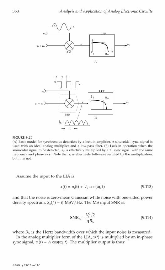
368 Analysis and Application of Analog Electronic Circuits
Assume the input to the LIA is
x(t) = ni(t) + Vs cos(wo t) (9.113)
and that the noise is zero-mean Gaussian white noise with one-sided powerdensity spectrum, Sn(f ) = h MSV/Hz. The MS input SNR is:
(9.114)
where Bin is the Hertz bandwidth over which the input noise is measured.In the analog multiplier form of the LIA, x(t) is multiplied by an in-phase
sync signal, vs(t) = A cos(wo t). The multiplier output is thus:
FIGURE 9.20(A) Basic model for synchronous detection by a lock-in amplifier. A sinusoidal sync. signal isused with an ideal analog multiplier and a low-pass filter. (B) Lock-in operation when thesinusoidal signal to be detected, s1, is effectively multiplied by a ±1 sync signal with the samefrequency and phase as s1. Note that s1 is effectively full-wave rectified by the multiplication,but n1 is not.
Bout
Bout
f
f
00
00
LPF
1vo
AM
s1 + n1
s1 + n1
+1
PSR
1
vs LPF
voy
y
A
vs
T
−1
T
s1B
A
SNRins
in
VB
=2 2
h
© 2004 by CRC Press LLC

Noise and the Design of Low-Noise Amplifiers for Biomedical Applications 369
(9.115)
Note that the one-sided power spectrum of the first term in Equation9.115 is the noise PDS shifted up to be centered at w = wo. Because Sn(f )is white, shifting the center of Sn(f ) from 0 to fo = wo/2p does not changethe noise output of the LIA’s output band-pass filter. Thus, the MS outputnoise voltage from the LIA is von
2 = A2 h(1/4t) MSV, where (1/4t) can beshown to be the equivalent noise Hertz bandwidth of the simple output R–Clow-pass filter, and t is the output LPF’s time constant. The output LPFremoves the 2wo frequency term in the right-hand term of Equation 9.115,leaving a dc output proportional to the peak value of the sinusoidal signal.Clearly, vos = AVs/2. Thus, the MS SNR at the LIA output is:
(9.116)
The noise figure, F, is defined as the ratio of SNRin to SNRout. For anamplifier, F should be as small as possible. In a noise-free amplifier (thelimiting case), F = 1. It is easy to show that F for this kind of LIA is:
FLIA = Bout/Bin (9.117)
where Bout = 1/4t is the Hertz noise bandwidth of the LIA’s output LPF andBin is the Hertz noise bandwidth over which the input noise is measured.Because the LIA’s desired output is a dc signal proportional to the peaksinusoidal input signal, Bout can be on the order of single Hertz and FLIA canbe 1.
In the second model for LIA noise, consider the synchronous rectifier LIAarchitecture of Figure 9.20(B). Now the sinusoidal signal is full-wave rectifiedby passing it through an absolute value function that models the synchro-nous rectifier. The full-wave rectified sinusoidal input signal can be shownto have the Fourier series (Aseltine, 1958):
(9.118)
Clearly, the average or dc value of y is Vs (2/p).Curiously, the zero-mean white noise is not conditioned by the absval
function of the synchronous rectifier. This is because the synchronous rectifier
y v n s A t n t V t
An t t AV t
y t An t t AV t
s i i o i s o
o s o
i o s o
= +( ) = ( ) ( ) + ( )[ ]= ( ) ( ) + ( )
( ) = ( ) ( ) + ( ) + ( )[ ]
cos cos
cos cos
cos cos
w w
w w
w w
2
2 1 2
SNRouts
s
A VA
V= ( ) =2 2
224
1 4h tt h
y t v t V t ts s o o( ) = ( ) = ( ) - ( ) ( ) - ( ) ( ) - º[ ]2 1 2 3 2 2 15 4p w wcos cos
© 2004 by CRC Press LLC
370 Analysis and Application of Analog Electronic Circuits
is really created by effectively multiplying x(t) = ni (t) + Vs cos(wot) by aneven ±1 square wave having the same frequency as, and in phase with, Vs
cos(wo t). This square wave can be represented by the Fourier series:
(9.119)
where wo = 2p/T and
(9.120)
For a unit cosine (even) square wave that can be written in expanded form,
(9.121)
The input Gaussian noise is multiplied by SQWV(t):
(9.122)
Before passing through the LIA’s output LPF, the white one-sided noisepower density spectrum can be shown to be:
(9.123)
This white noise is conditioned by the output LPF, so the output MS SNR is:
(9.124)
The MS SNR at the input to the LIA is:
(9.125)
SQWV t a n tn on
( ) = ( )=
•
 cos w1
a T f t n t dt n nn o
T
T
= ( ) ( ) ( ) = ( ) ( ) [ ]-Ú2 4 2
2
2
cos sinw p p nonzero for n odd
SQWV t
t t t to o o o
( ) =
( ) ( ) - ( ) ( ) + ( ) ( ) - ( ) ( ) + º[ ] cos cos cos cos4 1 3 3 1 5 5 1 7 7p w w w w
y t n t
t t t t
n
o o o o
( ) = ( ) ¥ ( )( ) - ( ) ( ) + ( ) ( ) - ( ) ( ) + º[ ]
4
1 3 3 1 5 5 1 7 7
p
w w w w cos cos cos cos
S fn( ) = ( ) - ( ) + ( ) - ( ) + ( ) - ( ) + ( ) - º[ ]=
h p
h
4 1 1 3 1 5 1 7 1 9 1 11 1 132 2
MSV Hz
SNRouts
out
VB
= ( )2 22 p
h
SNRins
in
VB
=2 2
h
© 2004 by CRC Press LLC
Noise and the Design of Low-Noise Amplifiers for Biomedical Applications 371
Thus, F for this LIA architecture is found to be:
(9.126)
which can be made quite small by adjusting the ratio of Bout to Bin.As an example of signal recovery by an LIA, consider an LIA of the analog
multiplier architecture. Let the signal to be measured be vs(t) = 20 ¥ 10-9
cos(2p 50 ¥ 103 t). The Gaussian white noise present with the signal has aroot power spectrum of ÷h = 4 nVRMS/÷Hz. The input amplifier has avoltage gain of Kv = 104 with a 100-kHz noise and signal bandwidth. Thus,the raw input MS SNR is:
(9.127)
If the sinusoidal signal is conditioned by an (ideal) unity-gain LPF with aQ = 50 = center freq./bandwidth, the noise bandwidth B = 50 ¥ 103/50 =1 kHz. The MS SNR at the output of the ideal BPF is still poor:
(9.128)
Now the signal plus noise is amplified and passed directly into the LIAand the LIA’s output LPF has a noise bandwidth of 0.125 Hz. The output dccomponent of the signal is KvVs/2 V. Thus, the MS dc output signal is =Kv
2 Vs2/4 = Kv
2 ¥ 1 ¥ 10-16 MSV. The MS noise output is = Kv2 (4 ¥ 10-9)2 ¥
0.125 MSV; the MS SNRout = 50, or +17 dB.The costs for using an LIA are that the ac signal is reduced to a proportional
dc level and that the output LPF means that the LIA does not reach a newsteady-state output, given a change in Vs, until about three time constantsof the LPF (about 3 sec in the preceding example). The benefit of using anLIA is that coherent signals buried in up to 60-dB noise can be measured.
9.8.7 Signal Averaging of Evoked Signals for Signal-to-Noise Ratio Improvement
9.8.7.1 Introduction
The signal-to-noise ratio (SNR) of a periodic signal recorded with additivenoise is an important figure of merit that characterizes the expected resolutionof the signal. SNRs are typically given at the input to a signal conditioningsystem, as well as at its output. SNR can be expressed as a positive realnumber or in decibels (dB). The SNR can be calculated from the MS, RMS,or peak signal voltage divided by the MS or RMS noise voltage in a defined
FBB
BB
in
out
out
in
out
in
= = =SNRSNR
p2
1 233 .
SNR MSV MSV
or dBin1
9 2
9 5
16
12420 10 2
4 10 102 10
1 6 101 25 10 39=
¥( )¥( ) ¥
= ¥¥
= ¥ --
-
-
--
.. ,
SNR MSV
or dBfi t1
16
9 2 3
22 10
4 10 101 25 10 19= ¥
¥( ) ¥= ¥ -
-
--. ,
vso2
vno2
© 2004 by CRC Press LLC

372 Analysis and Application of Analog Electronic Circuits
noise bandwidth. If the MS SNR is computed, the SNR(dB) = 10 log10
(msSNR); otherwise it is SNR(dB) = 20 log10(RMSSNR)Signal averaging is widely used in experimental and clinical electrophysiol-
ogy in order to extract a repetitive, quasi-deterministic, electrophysiologicaltransient response buried in broadband noise. One example of the type of signalextracted is the evoked cortical response recorded directly from the surface ofthe brain (or from the scalp) by an electrode pair while the subject is given arepetitive periodic sensory stimulus, such as a tone burst, flash of light, ortachistoscopically presented picture. Every time the stimulus is given, a “hard-wired” electrophysiological transient voltage, sj(t), lasting several hundred MSis produced in the brain by the massed activity of cortical and deeper neurons.When viewed directly on an oscilloscope or recorder, each individual evokedcortical response is invisible to the eye because of the accompanying noise.
Signal averaging is generally used to extract the evoked potential, s(t),from the noise accompanying it. Signal averaging is also used to extractevoked cortical magnetic field transients recorded with SQUID sensors(Northrop, 2002) and to extract multifocal electroretinogram (ERG) signalsobtained when testing the competence of macular cones in the retina of theeye. A small spot of light illuminating only a few cones is repetitively flashedon the macular retina. ERG averaging is done over N flashes for a given spotposition in order to extract the local ERG flash response, then the spot ismoved to a new, known position on the macula and the process is repeateduntil a 2-D macular ERG response of one eye is mapped (Northrop, 2002).
Signal averaging is ensemble averaging; following each identical periodicstimulus, the response can be written for the jth stimulus:
xj(t) = sj(t) + nj(t), 0 £ j £ N (9.129)
where sj (t) is the jth evoked transient response and nj(t) is the jth noise fol-lowing the stimulus. t is the local time origin taken as 0 when the jth stimulusis given.
The noise is assumed to be generally nonstationary, i.e., its statistics areaffected by the stimulus. Assume that the noise has zero mean, however,regardless of time following any stimulus, i.e., En(t) = 0, 0 £ t < Ti. Ti is theinterstimulus interval. Also, to be general, assume that the evoked responsevaries from stimulus to stimulus; that is, sj(t) is not exactly the same as sj+1(t), etc.
Each xj(t) is assumed to be sampled and digitized beginning with eachstimulus; the sampling period is Ts and M samples are taken following eachstimulus. Thus, there are N sets of sampled xj(k), 0 £ k £ (M - 1); also, (M -1)Ts = TD < Ti. TD is the total length of analog xj(t) digitized following eachinput stimulus (epoch length).
When the jth stimulus is given, the x(k)th value is summed in the kth dataregister with the preceding x(k) values. At the end of an experimental run,[x1(k) + x2(k) + x3(k) +… + xN(k)] in the kth
the organization of a signal averager. Early signal averagers were stand-alone dedicated instruments. Modern signal averagers typically use a PC or
© 2004 by CRC Press LLC
data register. Figure 9.21 illustrates
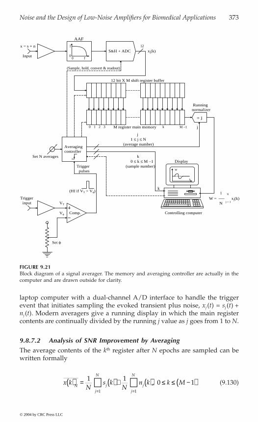
Noise and the Design of Low-Noise Amplifiers for Biomedical Applications 373
laptop computer with a dual-channel A/D interface to handle the triggerevent that initiates sampling the evoked transient plus noise, xj (t) = sj (t) +nj (t). Modern averagers give a running display in which the main registercontents are continually divided by the running j value as j goes from 1 to N.
9.8.7.2 Analysis of SNR Improvement by Averaging
The average contents of the kth register after N epochs are sampled can bewritten formally
(9.130)
FIGURE 9.21Block diagram of a signal averager. The memory and averaging controller are actually in thecomputer and are drawn outside for clarity.
AAF
12 bit X M shift register buffer
Vφ
Triggerinput
(Sample, hold, convert & readout)
S&H + ADC121
f0
0
xj(k)x = s + n
Input
Controlling computer
M register main memory M −10 1 2 3
VT
(HI if VT > Vφ) 1 N
W = xj(k)N j = 1
Set φ
k
W
k
Comp.
k0 ≤ k ≤ M −1
Set N averages
Averagingcontroller
Display
j
(sample number)
k
(average number)
Triggerpulses
j1 ≤ j ≤ N
Runningnormalizer
÷ j
x kN
s kN
n k k MN jj
N
jj
N
( ) = ( ) + ( ) £ £ -( )= =
 Â1 10 1
1 1
,
© 2004 by CRC Press LLC
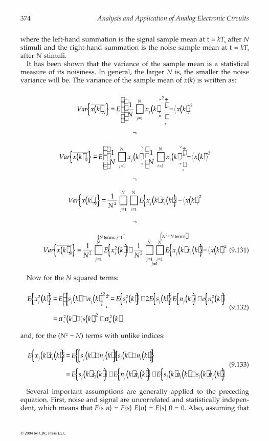
374 Analysis and Application of Analog Electronic Circuits
where the left-hand summation is the signal sample mean at t = kTs after Nstimuli and the right-hand summation is the noise sample mean at t = kTs
after N stimuli.It has been shown that the variance of the sample mean is a statistical
measure of its noisiness. In general, the larger N is, the smaller the noisevariance will be. The variance of the sample mean of x(k) is written as:
Ø
Ø
Ø
(9.131)
Now for the N squared terms:
(9.132)
and, for the (N2 - N) terms with unlike indices:
(9.133)
Several important assumptions are generally applied to the precedingequation. First, noise and signal are uncorrelated and statistically indepen-dent, which means that Es n = Es En = Es 0 = 0. Also, assuming that
Var x k EN
x k x kN jj
N
( ) = ( )È
ÎÍÍ
˘
˚˙˙
ÏÌÔ
ÓÔ
¸˝Ô
Ô- ( )
=Â1
1
2
2
Var x k EN
x kN
x k x kN jj
N
ii
N
( ) = ( )È
ÎÍÍ
˘
˚˙˙
( )È
ÎÍÍ
˘
˚˙˙
ÏÌÔ
ÓÔ
¸˝Ô
Ô- ( )
= =Â Â1 1
1 1
2
Var x kN
E x k x k x kN j ii
N
j
N
( ) = ( ) ( ) - ( )==
ÂÂ12
11
2
Var x kN
E x kN
E x k x k x kN jj
NN j
j ii
j
N
j
NN N
( ) = ( ) + ( ) ( ) - ( )=
=( )
=π
=
=( )
 ÂÂ1 12
2
1
1
21
11
2
2 terms, terms
E x k E s k n k E s k E s k E n k e n k
k s k k
j j j j j j j
s n
22
2 2
2 2 2
2( ) = ( ) + ( )[ ]ÏÌÓ¸˛
= ( ) + ( ) ( ) + ( ) = ( ) + ( ) + ( )s s
E x k x k E s k n k s k n k
E s k s k E n k n k E s k n k s k n k
j i j j i i
j i j i j i i j
( ) ( ) = ( ) + ( )[ ] ( ) + ( )[ ] = ( ) ( ) + ( ) ( ) + ( ) ( ) + ( ) ( )
© 2004 by CRC Press LLC
Noise and the Design of Low-Noise Amplifiers for Biomedical Applications 375
noise samples taken at or more than t = T seconds apart will be uncorrelatedleads to Enj(k) ni (k) = Enj (k) Eni (k) Æ 0. So, Exj (k) xi (k) = E[sj (k) si (k).It is also assumed that sj (k) and si (k) taken at or more than T seconds apartare independent. So finally:
(9.134)
Now, putting all the terms together:
(9.135A)
Ø
(9.135B)
The variance of the sample mean for the kth sample following a stimulusis a measure of the noisiness of the averaging process. The variance of theaveraged signal, x, is seen to decrease as 1/N, where N is the total numberof stimuli given and of responses averaged.
Another measure of the effectiveness of signal averaging is the noise factor,
F ∫ , where Sin is the mean-squared input signal to the averaging process;
Nin is the MS input noise; So is the MS output signal; and No is the MS outputnoise. The noise factor is normally used as a figure of merit for amplifiers.Because amplifiers generally add noise to the input signal and noise, theoutput signal-to-noise ratio (SNR) is less than the input SNR; thus, for anonideal amplifier, F > 1. For an ideal noiseless amplifier, F = 1. The exceptionto this behavior is in signal averaging, in which the averaging process gen-erally produces an output SNR greater than the input SNR, making F < 1.Note that the noise figure of a signal conditioning system is defined as:
NF ∫ 10 log10(F) dB (9.136)
From the preceding calculations on the averaging process:
(9.137)
(9.138)
(9.139)
E x k x k E s k s k E s k E s k s kj i j i j i( ) ( ) = ( ) ( )[ ] = ( ) ( ) = ( )2
Var x kN
N k s k k N N s k s kN s n( ) = ( ) + ( ) + ( )ÈÎÍ
˘˚
+ -( ) ( )ÏÌÓ¸˛
- ( )12
2 2 2 2 2 2s s
Var x kk k
NNs n( ) = ( ) + ( )s s2 2
S NS Nin in
o o
S k E s k k s kin j s( ) = ( ) = ( ) + ( )2 2 2s
N k E n k kin j n( ) = ( ) = ( )2 2s
S k E s kk
Ns ko o
s( ) = ( ) = ( ) + ( )22 2s
© 2004 by CRC Press LLC

376 Analysis and Application of Analog Electronic Circuits
(9.140)
These terms can be put together to calculate the noise factor of the aver-aging process:
(9.141)
Note that if the evoked transient is exactly the same for each stimulus,ss
2(k) Æ 0 and F = 1/N.The reader should appreciate that this is an idealized situation; in practice,
a constant level of noise, sa2, is present on the output of the signal averager.
This noise comes from signal conditioning amplifiers, quantization accom-panying analog-to-digital conversion, and arithmetic round-off. The aver-ager MS output noise can thus be written:
(9.142)
and, as before, the MS signal is:
(9.143)
The averaged MS output SNR is just:
(9.144)
and, if the evoked response is deterministic, ss2(k) Æ 0, then:
(9.145)
Note that if the number, N, of stimuli and responses averaged becomesvery large, then
(9.146)
N kk k
Non s( ) = ( ) + ( )s s2 2
Fk s k k k
k N s k
s s n
s
=( ) + ( )È
Î͢˚
+ ( ) ( )[ ]( ) + ( )[ ]
s s s
s
2 2 2 2
22
1
Nk k
Non s
a= ( ) + ( ) +s s
s2 2
2 mean-squared volts
S kk
Ns ko
s( ) = ( ) + ( )s 2 2
SNRos
s n a
k Ns kk k N
= ( ) + ( )( ) + ( ) +s
s s s
2 2
2 2 2
SNRon a
N s kk N
= ( )( ) +
2
2 2s s
SNRoa
s kÆ ( )2
2s
© 2004 by CRC Press LLC
Noise and the Design of Low-Noise Amplifiers for Biomedical Applications 377
and also in the limit,
. (9.147)
Signal averaging can recover a good estimate of s(k) even when sn(k) is60 dB larger than s(k). From Equation 9.145, it is possible to find the Nrequired to give a specified SNRo, given sn
2(k), sa2 and .
9.8.7.3 Discussion
Signal averaging is widely used in biomedical research and diagnosis. Aperiodic stimulus (e.g., noise, flash, electric shock, pin prick, etc.) is given toa subject. The response is generally electrophysiological, i.e., an evokedcortical potential (ECP), an electrocochleogram (ECoG), or an electroretino-gram (ERG) — all richly contaminated with noise. By averaging, the noiseis reduced (its sample mean tends to zero) as the number of averaging cycles,N, increases, while the signal remains the same. Thus, signal averagingincreases the SNR in the averaged signal. However, as demonstrated, thereare practical limits to the extent of SNR improvement.
9.9 Some Low-Noise Amplifiers
TABLE 9.2
Partial Listing of Commercially Available Low-Noise Op Amps and Instrumentation Amplifiers with Low-Noise Characteristics Suitable for Biomedical Signal Conditioning Applications
Amp. Model Typea enab ina
c
Low freq Vn
d Rine fT
f AV0g
PMI 0P-27 OP/BJT 3 0.4 pA 0.08 mVppk 6 M 5 106
PMI OP-61A OP/BJT 3.4 0.8 pA — — 200 4 ¥ 105
HA 5147A OP/BJT 3 0.4 pA 0.08 mVppk 6M 140 106
BB OPA111BM OP/FET 6 0.4 fA 1.6 mVppk 1013 (DM); 1014 (CM)
2 125 dB
LT1028 OP/BJT 0.85 1 pA 35 nVppk 20M (DM); 300M (CM)
75 7 ¥ 106
AM-427 OP/BJT 3 0.4 pA 0.18 mVppk 1.5M (DM) 5 120 dBNE5532 OP/BJT 5 0.7 pA — 300K 10 105
MAX 4106/7 OP/BJT 0.75 2.5 pA — 1 MW (CM) 300 (–3) 105
PMI AMP-011 IA/BJT 5 0.15 pA 0.12 mVppk 10G (DM); 20G (CM)
26 1 – 103
PMI AMP-021 IA/FET 9 0.4 fA 0.4 mVppk 10G (DM); 16.5G (CM)
5 1 – 103
AD624 IA/BJT 4 60 pAppk; 0.1–10 Hz
10 nVppk 1G˜Á10 pF (CM & DM)
1 1 – 103
Fk
a
n
Æ ( )s
s
2
2
s k( )2
© 2004 by CRC Press LLC
378 Analysis and Application of Analog Electronic Circuits
9.10 The Art of Low-Noise Signal Conditioning System Design
9.10.1 Introduction
Consider the scenario in which a physiological signal such as nerve actionpotentials (spikes) is to be recorded extracellularly from the brain with ametal microelectrode embedded in the cortex. The signal has a peak ampli-tude, vspk, generally in the tens of microvolts. The input signal is assumedto be accompanied by additive white noise and to be resolved above thetotal broadband noise at the preamplifier’s input. It has been shown previ-ously that the MS input noise is:
Ni = [ena2 + ina
2 Rs2 + 4kTRs + ens
2] B MSV. (9.148)
where ena and ina are white root noise spectra that are properties of theamplifier used and ens is a white noise root power spectrum added to therecorded signal in the brain.
It is also assumed that the thermal noise in the source resistance, Rs, iswhite and B is the Hertz bandwidth over which the signal and input noisesare considered. Low-noise amplifier design is particularly desired when vspk
< 3 .
TABLE 9.2 (continued)
Partial Listing of Commercially Available Low-Noise Op Amps and Instrumentation Amplifiers with Low-Noise Characteristics Suitable for Biomedical Signal Conditioning Applications
Amp. Model Typea enab ina
c
Low freq Vn
d Rine fT
f AV0g
AD6251 IA/BJ 4 0.3 pA 0.2 mV 1G (DMandCM) 25 1 – 103
BB INA1102 IA/FET 10 1.8 fA 1 mVppk 2 ¥ 1012 (DM); 5 ¥ 1012 (CM)
12 1 – 500
PMI AMP-052 IA/FET 16 10 fA 4 mVpp 1012 (DM & CM) 3 1 – 103
ZN459CP IA/BJT 0.8 1 pA — 7k (Single ended) 15(–3) 60 dBZN424 IA/BJT 5.5 0.3 pA — 200k 4 2 ¥ 104
a Type refers to whether the amplifier is an op amp (OP) or an instrumentation amplifier (IA),and whether it has a BJT or FET headstage.
b ena is given in nV RMS/÷Hz measured at 1 kHz.c ina is given in picoamps (pA) or femtoamps (fA) RMS/÷Hz measured at 1 kHz.d Low freq. Vn is the equivalent peak-to-peak, short-circuit input noise measured over a standard
0.1- to 10-Hz bandwidth.e Rin is the input resistance.f fT is the unity gain bandwidth in MHz, unless followed by (–3), in which case it is the high-
frequency -3-dB frequency.g AV0 for op amps is their open-loop dc gain; the useful gain range is given for IAs.
ena2 ina
2 Rs2 4kTRs++[ ]B V
© 2004 by CRC Press LLC
Noise and the Design of Low-Noise Amplifiers for Biomedical Applications 379
The first step in designing a low-noise signal conditioning system is tochoose a low-noise headstage amplifier that also meets other design criteriafor parameters such as bandwidth, slew rate, input dc offset voltage (VOS)and bias current (IB), and VOS and IB tempcos. Modern low-noise IC amplifierstypically have enas < 7 nV/÷Hz in the white region. Such amplifiers may usesuper beta BJT headstages that, unlike FET headstages, have higher valuesof IB and ina and a relatively lower Rin
Because the noise performance of a multistage amplifier used for signalconditioning is set by the noise characteristics of the (input) headstage, it isnecessary to give the low-noise headstage at least a gain of 5, preferably 10.Having done this, following amplifier stages need not be expensive low-noise types. Any resistance used in an input high-pass filter coupling theelectrode to the headstage should be a low-noise metal film type, not carboncomposition.
Finally, a band-pass filter with noise bandwidth B should follow the ampli-fier stages. The filter’s corner frequencies to pass nerve spikes and to excludehigh- and low-frequency noise should be at 30 Hz and 3 kHz. The noiseHertz BW, B, is generally close to but greater than the signal passband. Fora simple two-real-pole BPF with low break frequency at flo = 1/(2pt1) Hz and
hi 2
. (9.149)
The signal’s -3-dB Hz bandwidth is easily seen to be:
(9.150)
For example, if t2 = 10-4 sec and t1 = 10-2 sec then B = 2.475 ¥ 103 Hz fornoise and the signal BW is SBW = 1.576 ¥ 103 Hz.
Section 9.4.3 described the use of an input transformer to maximize theSNR at the output of the analog signal conditioning system. It may beworthwhile to consider transformer coupling of the source to the headstageif the Thevenin source resistance of the electrode, Rs, is less than 1/10 of Rsopt =ena/ina W. Transformer coupling carries a price tag, however. Special expen-sive, low-loss, low-noise transformers are used that generally have extensivemagnetic shielding to prevent the pick-up of unwanted, time-varying mag-netic fields, such as those from power lines, etc. The author has never heardof SNRo-maximizing coupling transformers being used with metal micro-electrodes. The Rs of a typical metal microelectrode is on the order of 15 kWwith its tip platinized (Northrop and Guignon, 1970). If an instrumentationamplifier such as the AD624 is used as the headstage, its ena = 4 nV/÷Hz and
B =+( )1
4 12 2 1t t t Hz
SBW Hz=-( )t t
p t t1 2
1 22
© 2004 by CRC Press LLC
. See Table 9.2 for examples.
a high break frequency at f = 1/(2pt ) Hz, the noise BW from Table 9.1 is:
380 Analysis and Application of Analog Electronic Circuits
its ina = 0.4 pA/÷Hz, so its Rsopt = ena/ina = 105 W. If a transformer were to beused, its turns ratio to maximize SNRout would be 2.58.
Experience indicates that, although SNRout improvement would occur, itwould be too small to justify the expense of the transformer. (It would beonly 1.08 times the SNR of the amplifier with no transformer.) On the otherhand, if the same amplifier were to be used with a transducer having Rs =10 W, the transformer turns ration would be no = 100 and the improvementin SNRout over an amplifier with no transformer would be:
(9.151)
Thus, the use of the transformer under the preceding conditions wouldlead to a significant improvement in the output MS SNR.
Section 9.7 and Section 9.8.2 examined the effect of negative feedbackapplied around an amplifier through a resistive voltage divider. A surprisingresult was found for a sinusoidal voltage source connected to a standardinverting, ideal op amp circuit with short-circuit equivalent input noise rootpower spectrum, ena (ina = 0 in this case) and noisy resistors. Namely, theamplifier’s SNRout increases monotonically with amplifier gain magnitude,RF/R1, to a best asymptotic value of:
(9.152)
Thus the output MS SNR depends on the absolute value of the inputresistor and the amplifier’s overall closed-loop gain.
As a design example, examine the SNRout for an op amp used in thenoninverting mode. Although both op amp inputs are properly characterizedwith their own ena and ina, it is common practice to assume infinite CMRRand combine the noises as one net ena and ina at the amplifier’s summing
thermal white noise and that the signal is sinusoidal. The MS output signal is:
(9.153)
The MS output noise has five independent components:
(9.154)
r =+ +
+
= ¥ + ¥ + ¥ ¥¥ + ¥ ¥ ¥ ¥ ¥
=- - -
- - -
44 2
1 656 10 16 10 16 10 1001 656 10 2 4 10 4 10 10
81 81
2 2 2
19 18 26
19 9 13
kTR e i RkTR e i R
s na na s
s na na s
..
.
SNRoutmax =( )
+V B
kTR es
na
2
12
2
4
S V R Ro s F= ( ) +( )21
22 1 MSV
N kTR e R R i kTG kTG G Bo s na F na F F= +( ) +( ) + + +( ) 4 1 4 421
2 21
2 MSV
© 2004 by CRC Press LLC
junction, as shown in Figure 9.22. Assume that the three resistors make

Noise and the Design of Low-Noise Amplifiers for Biomedical Applications 381
Now the output MS SNR can be written:
(9.155)
where (RFR1) = RF R1/(RF + R1). SNRout is maximized by (1) choosing an op amp with low ina and ena; and
(2) making (RFR1) small. The latter condition says nothing about the ampli-fier’s voltage gain, (1 + RF/R1), only that RF R1/(RF + R1) must be small. Forexample, for small-signal operation, let R1 = 100 W, and RF = 99.9 kW, for again of 103. RF and R1 should be low XS noise types, i.e., wire-wound ormetal film.
Low noise amplifier design also includes strategies to minimize the pick-up of coherent interference. These strategies are not covered here; the inter-ested reader can find descriptions of shielding, guarding, and ground loopelimination in Section 3.9 in Northrop (1997), and also in Barnes (1987) andOtt (1976).
9.11 Chapter Summary
This chapter introduced key mathematical ways of describing the randomnoise accompanying recorded signals and also originating in resistors andamplifiers. Concepts, properties, and significance of the probability densityfunction, auto- and cross-correlation functions and their Fourier transforms,and auto- and cross-power density spectrums were examined.
Random noise was shown to arise in all resistors, the real parts of imped-ances or admittances, diodes, and active devices including BJTs, FETs, and
FIGURE 9.22Noisy noninverting op amp amplifier relevant to the design example in Section 9.10.
RF @ T
R1 @ T
Rs @ T vi
vi’ena
ina
IOAVs
Vo
SNRouts
s na na F F
V B
kTR e i R R kT R R=
( )+ + ( ) + ( )
2
2 21
2
1
2
4 4
© 2004 by CRC Press LLC
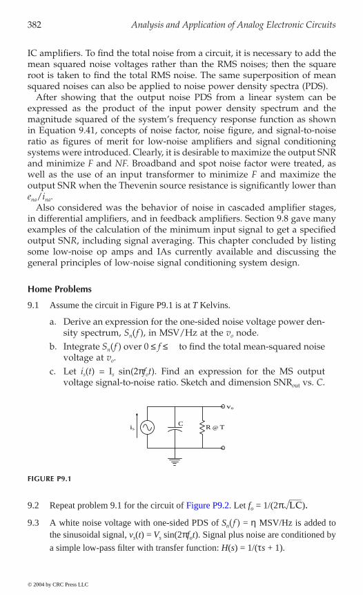
382 Analysis and Application of Analog Electronic Circuits
IC amplifiers. To find the total noise from a circuit, it is necessary to add themean squared noise voltages rather than the RMS noises; then the squareroot is taken to find the total RMS noise. The same superposition of meansquared noises can also be applied to noise power density spectra (PDS).
After showing that the output noise PDS from a linear system can beexpressed as the product of the input power density spectrum and themagnitude squared of the system’s frequency response function as shownin Equation 9.41, concepts of noise factor, noise figure, and signal-to-noiseratio as figures of merit for low-noise amplifiers and signal conditioningsystems were introduced. Clearly, it is desirable to maximize the output SNRand minimize F and NF. Broadband and spot noise factor were treated, aswell as the use of an input transformer to minimize F and maximize theoutput SNR when the Thevenin source resistance is significantly lower thanena/ina.
Also considered was the behavior of noise in cascaded amplifier stages,in differential amplifiers, and in feedback amplifiers. Section 9.8 gave manyexamples of the calculation of the minimum input signal to get a specifiedoutput SNR, including signal averaging. This chapter concluded by listingsome low-noise op amps and IAs currently available and discussing thegeneral principles of low-noise signal conditioning system design.
Home Problems
9.1 Assume the circuit in Figure P9.1 is at T Kelvins.
a. Derive an expression for the one-sided noise voltage power den-sity spectrum, Sn(f ), in MSV/Hz at the vo node.
b. Integrate Sn(f ) over 0 £ f £ • to find the total mean-squared noisevoltage at vo.
c. Let is(t) = Is sin(2pfot). Find an expression for the MS outputvoltage signal-to-noise ratio. Sketch and dimension SNRout vs. C.
9.2 o ).
9.3 A white noise voltage with one-sided PDS of Sn(f ) = h MSV/Hz is added tothe sinusoidal signal, vs(t) = Vs sin(2pfot). Signal plus noise are conditioned by
a simple low-pass filter with transfer function: H(s) = 1/(ts + 1).
FIGURE P9.1
is R @ TC
vo
LC
© 2004 by CRC Press LLC
Repeat problem 9.1 for the circuit of Figure P9.2. Let f = 1/(2p
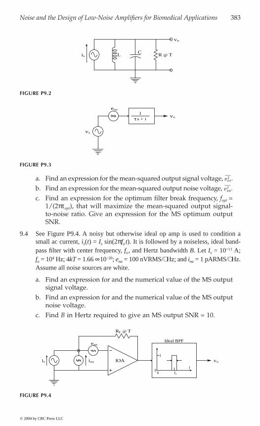
Noise and the Design of Low-Noise Amplifiers for Biomedical Applications 383
a. Find an expression for the mean-squared output signal voltage, .b. Find an expression for the mean-squared output noise voltage, .c. Find an expression for the optimum filter break frequency, fopt =
1/(2ptopt), that will maximize the mean-squared output signal-to-noise ratio. Give an expression for the MS optimum outputSNR.
9.4 See Figure P9.4. A noisy but otherwise ideal op amp is used to condition asmall ac current, is(t) = Is sin(2pfot). It is followed by a noiseless, ideal band-pass filter with center frequency, fo, and Hertz bandwidth B. Let Is = 10-11 A;fo = 104 Hz; 4kT = 1.66 ¥ 10-20; ena = 100 nVRMS/÷Hz; and ina = 1 pARMS/÷Hz.Assume all noise sources are white.
a. Find an expression for and the numerical value of the MS outputsignal voltage.
b. Find an expression for and the numerical value of the MS outputnoise voltage.
c. Find B in Hertz required to give an MS output SNR = 10.
FIGURE P9.2
FIGURE P9.3
FIGURE P9.4
R @ TC
vo
is L
1τ s + 1
ena
vs
vo
vos2
von2
ffo0
0
1IOA
RF @ T
ena
inais vo
Ideal BPF
© 2004 by CRC Press LLC

384 Analysis and Application of Analog Electronic Circuits
9.5 A tuned (band-pass) video amplifier, shown in Figure P9.5, is used tocondition a 900-kHz Doppler ultrasound signal to which various uncorrelatednoise signals are added. The amplifier’s peak gain is 104 and its noisebandwidth B is 10 kHz centered on 900 kHz. Let ena = 10 nVRMS/÷Hz(white); ens = 25 nVRMS/÷Hz (white); Rs = 1200 W; 4kT = 1.66 ¥ 10-20; andvs(t) = Vs sin(2p 9.01 ¥ 105 t).
a. Find the RMS output noise voltage.b. Find the peak signal voltage, Vs, to give an RMS SNRout = 10.
9.6 A noisy but otherwise ideal op amp is used to condition the signal from asilicon photoconductor (PC) light sensor as shown in Figure P9.6. Resistor Rc
is used to compensate for the PC’s dark current so that Vos = 0 in the dark. ina =0.4 pARMS/÷Hz (white); ena = 3 nVRMS/÷Hz (white); Rc = 2.3 ¥ 105 W; RF =106 W; and 4kT = 1.66 ¥ 10-20. The photoconductor can be modeled by a fixeddark conductance, GD = 1/RD, in parallel with a light-sensitive conductancegiven by GP = IP/VC = PL ¥ 742.27 S. PL is the incident optical power in wattsand the photoconductance parameter is computed from various physical
noiseless LPF with t = 0.01 sec.
FIGURE P9.5
FIGURE P9.6
ena
ens
vs
RS @ T Vo
BP Amp.
IOA
RF @ T
ina1
0.01s + 1
ena
LPF
Vo
+ 5 V− 5 V
PL
ICID GCIPGPGD
Photoconductor
© 2004 by CRC Press LLC
constants (see Section 2.6.5 in Chapter 2). The amplifier is followed by a
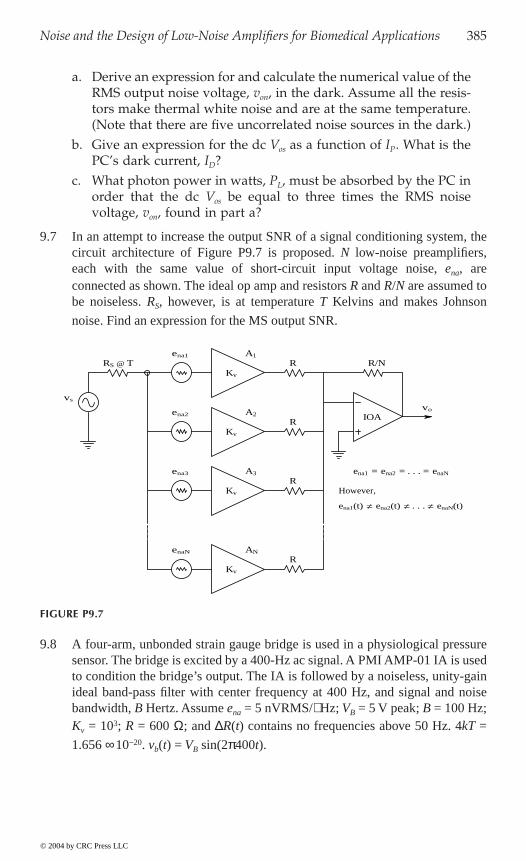
Noise and the Design of Low-Noise Amplifiers for Biomedical Applications 385
a. Derive an expression for and calculate the numerical value of theRMS output noise voltage, von, in the dark. Assume all the resis-tors make thermal white noise and are at the same temperature.(Note that there are five uncorrelated noise sources in the dark.)
b. Give an expression for the dc Vos as a function of IP. What is thePC’s dark current, ID?
c. What photon power in watts, PL, must be absorbed by the PC inorder that the dc Vos be equal to three times the RMS noisevoltage, von, found in part a?
9.7 In an attempt to increase the output SNR of a signal conditioning system, thecircuit architecture of Figure P9.7 is proposed. N low-noise preamplifiers,each with the same value of short-circuit input voltage noise, ena, areconnected as shown. The ideal op amp and resistors R and R/N are assumed tobe noiseless. RS, however, is at temperature T Kelvins and makes Johnson
noise. Find an expression for the MS output SNR.
9.8 A four-arm, unbonded strain gauge bridge is used in a physiological pressuresensor. The bridge is excited by a 400-Hz ac signal. A PMI AMP-01 IA is usedto condition the bridge’s output. The IA is followed by a noiseless, unity-gainideal band-pass filter with center frequency at 400 Hz, and signal and noisebandwidth, B Hertz. Assume ena = 5 nVRMS/÷Hz; VB = 5 V peak; B = 100 Hz;Kv = 103; R = 600 W; and DR(t) contains no frequencies above 50 Hz. 4kT =
1.656 ¥ 10-20. vb(t) = VB sin(2p400t).
FIGURE P9.7
ena1
ena2
enaN
R/N
vo
RS @ T
vs
IOA
R
R
R
R
Kv
Kv
Kv
Kv
A1
A2
AN
ena3 A3 ena1 = ena2 = . . . = enaN
ena1(t) ≠ ena2(t) ≠ . . . ≠ enaN(t)
However,
© 2004 by CRC Press LLC
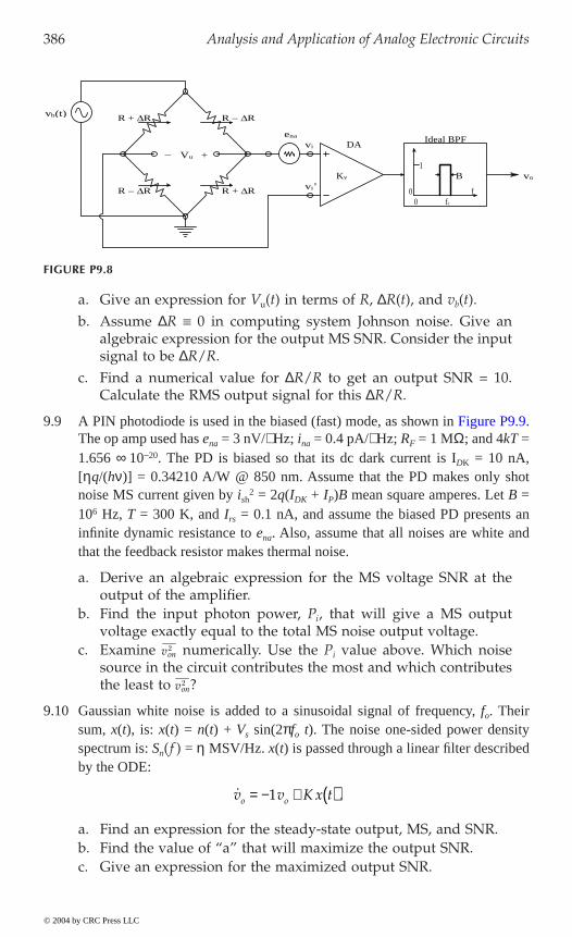
386 Analysis and Application of Analog Electronic Circuits
a. Give an expression for Vu(t) in terms of R, DR(t), and vb(t).b. Assume DR ∫ 0 in computing system Johnson noise. Give an
algebraic expression for the output MS SNR. Consider the inputsignal to be DR/R.
c. Find a numerical value for DR/R to get an output SNR = 10.Calculate the RMS output signal for this DR/R.
9.9The op amp used has ena = 3 nV/÷Hz; ina = 0.4 pA/÷Hz; RF = 1 MW; and 4kT =1.656 ¥ 10-20. The PD is biased so that its dc dark current is IDK = 10 nA,[hq/(hn)] = 0.34210 A/W @ 850 nm. Assume that the PD makes only shotnoise MS current given by ish
2 = 2q(IDK + IP)B mean square amperes. Let B =106 Hz, T = 300 K, and Irs = 0.1 nA, and assume the biased PD presents aninfinite dynamic resistance to ena. Also, assume that all noises are white andthat the feedback resistor makes thermal noise.
a. Derive an algebraic expression for the MS voltage SNR at theoutput of the amplifier.
b. Find the input photon power, Pi, that will give a MS outputvoltage exactly equal to the total MS noise output voltage.
c. Examine numerically. Use the Pi value above. Which noisesource in the circuit contributes the most and which contributesthe least to ?
9.10 Gaussian white noise is added to a sinusoidal signal of frequency, fo. Theirsum, x(t), is: x(t) = n(t) + Vs sin(2pfo t). The noise one-sided power densityspectrum is: Sn(f ) = h MSV/Hz. x(t) is passed through a linear filter describedby the ODE:
.
a. Find an expression for the steady-state output, MS, and SNR.b. Find the value of “a” that will maximize the output SNR.c. Give an expression for the maximized output SNR.
FIGURE P9.8
DA
vb(t)
−
Kv voB1
ffc
00
ena Ideal BPF
Vu +vi
vi’
R + ∆R
R + ∆R
R − ∆R
R − ∆R
von2
von2
v v K x to o= - + ( )1
© 2004 by CRC Press LLC
A PIN photodiode is used in the biased (fast) mode, as shown in Figure P9.9.
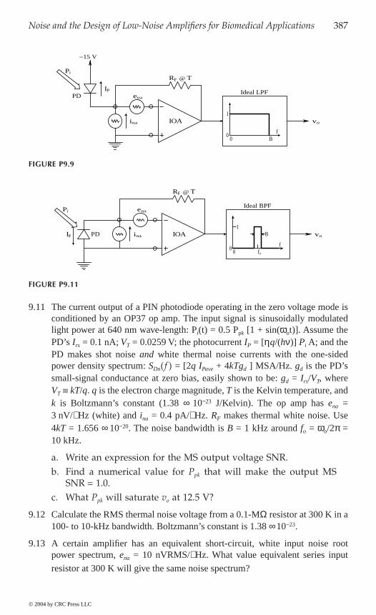
Noise and the Design of Low-Noise Amplifiers for Biomedical Applications 387
9.11 The current output of a PIN photodiode operating in the zero voltage mode isconditioned by an OP37 op amp. The input signal is sinusoidally modulatedlight power at 640 nm wave-length: Pi(t) = 0.5 Ppk [1 + sin(wot)]. Assume thePD’s Irs = 0.1 nA; VT = 0.0259 V; the photocurrent IP = [hq/(hn)] Pi A; and thePD makes shot noise and white thermal noise currents with the one-sidedpower density spectrum: SDn(f ) = [2q IPave + 4kTgd ] MSA/Hz. gd is the PD’ssmall-signal conductance at zero bias, easily shown to be: gd = Irs/VT, whereVT ∫ kT/q. q is the electron charge magnitude, T is the Kelvin temperature, andk is Boltzmann’s constant (1.38 ¥ 10-23 J/Kelvin). The op amp has ena =3 nV/÷Hz (white) and ina = 0.4 pA/÷Hz. RF makes thermal white noise. Use4kT = 1.656 ¥ 10-20. The noise bandwidth is B = 1 kHz around fo = wo/2p =10 kHz.
a. Write an expression for the MS output voltage SNR.b. Find a numerical value for Ppk that will make the output MS
SNR = 1.0.c. What Ppk will saturate vo at 12.5 V?
9.12 Calculate the RMS thermal noise voltage from a 0.1-MW resistor at 300 K in a100- to 10-kHz bandwidth. Boltzmann’s constant is 1.38 ¥ 10-23.
9.13 A certain amplifier has an equivalent short-circuit, white input noise rootpower spectrum, ena = 10 nVRMS/÷Hz. What value equivalent series input
resistor at 300 K will give the same noise spectrum?
FIGURE P9.9
FIGURE P9.11
f0
RF @ T
ena
vo
Pi
PD
1IOAina
0 B
−15 V
IP Ideal LPF
ffo0
0
1
RF @ T
ena
vo
Ideal BPFPi
IOAinaIP PD B
© 2004 by CRC Press LLC

388 Analysis and Application of Analog Electronic Circuits
9.14 An amplifier shown in Figure P9.14 has a 100-MW input resistance, ena = 12nVRMS/÷Hz, and a sinusoidal (Thevenin) source vs(t) in series with a 3.3-kWresistor. Both resistors are at 300 K. Amplifier bandwidth is 100 Hz to 20 kHz.Assume the resistors make white noise and that ena is white. The sinusoidalsource’s frequency is 1 kHz and the amplifier’s gain is 103. Find the RMSvalue of vs(t) so that the output mean-squared SNR = 1.
9.15 An OP-27 low-noise op amp is connected to a Thevenin source [vs, Rs @ T]through an ideal, noiseless transformer to maximize the MS output SNR.Consider the op amp ideal except for its noises. RF makes thermal noise. SeeFigure P9.15.
a. Give an expression for the mean-squared output signal voltage,. Hint: What is the Thevenin equivalent circuit looking back
from the summing junction toward the transformer?b. Give an expression for the MS output noise, .c. Find a numerical value for the transformer’s turns ratio, no, will
maximize SNRout. Let 4kT = 1.66 ¥ 10-20; RF = 105 W; ena = 3nVRMS/÷Hz (white); ina = 0.4 pARMS/÷Hz (white); Rs = 50 W;and the noise bandwidth B = 104 Hz.
9.16 Signal averaging: a periodically evoked transient signal, which can bemodeled by s(t) = (Vso/2)[1 + sin(2p t/T)] for 3T/4 £ t £ 7T/4, 0 elsewhere, isadded to Gaussian broad-band noise having zero mean and variance, sn
2.Assume the averager is noiseless (sa
2 = 0) and the signal is deterministic so itsvariance, ss
2 = 0.
FIGURE P9.14
FIGURE P9.15
ena
vi
vo
Kv vi
+
Rs
Rinvs(t)
100 MΩ
3.3 kΩ
vos2
von2
1: n
OP-27
ena
ina
Rs @ T
RF @ T
Vi’
Vs
Vo
© 2004 by CRC Press LLC

Noise and the Design of Low-Noise Amplifiers for Biomedical Applications 389
a. Find an algebraic expression for the number of averages, N,required to get a specified MS SNRout > 1 at the peak of the signal.
b. Evaluate N numerically so that when (Vso/2) = 1 mV and sn = 10mVRMS, the MS SNRout at peak s(t) will be 10.
© 2004 by CRC Press LLC
391
10Digital Interfaces
10.1 Introduction
Digital interfaces enable us to convert analog signals to a digital formatthat can be an input to a computer or a digital data storage system and,conversely, take digital data from a computer and convert it to an analogsignal (voltage, current, light intensity, etc.). An analog-to-digital converter(ADC) performs the former task, while a digital-to-analog converter (DAC)undertakes the latter operation. There are many types of ADCs and DACs.
The majority of ADC and DAC operations involve sampling, i.e., theperiodic conversion of signals to digital or analog format. Because sam-pling occurs in the time domain, it can also be described in the frequencydomain by appropriate transformation. Two major sources of error inperiodic data conversion will be discussed in this chapter: (1) a phenom-enon known as aliasing, in which an analog signal is effectively sampledtoo slowly for its bandwidth; and (2) a finite number of binary digits usedto characterize an analog signal; the finite-size binary words producequantization errors, effectively introducing noise into the sampled signal.The problem of aliasing in sampled data will be discussed first
10.2 Aliasing and the Sampling Theorem
10.2.1 Introduction
erally includes a digital computer that is used to supervise, coordinate, andcontrol the measurements, and which often is used to store (data logging),condition, and display data in a meaningful summary form on a monitor.In describing signal conversion interfaces, it is expedient first to considerdigital-to-analog converters (DACs) because these systems are also used inthe designs of several analog-to-digital converters (ADCs). Data conversion
© 2004 by CRC Press LLC
As shown in Figure 10.1, a modern biomedical instrumentation system gen-

392 Analysis and Application of Analog Electronic Circuits
from analog to digital form or digital to analog form is generally doneperiodically. Periodic data conversion has a great effect on the informationcontent of the converted data, as will be shown next.
10.2.2 The Sampling Theorem
The sampling theorem describes the analog filter required to recover ananalog signal, x(t), from its impulse-modulated (sampled) form, x*(t). Thetheorem states that if the highest frequency present in the CFT of y(t) is fmax,then when x(t) is sampled at a rate fs = 2 fmax, x(t) can be exactly recoveredfrom x*(t) by passing x*(t) through an ideal low-pass filter, HIL(j2pf).
The weighting function (impulse response) of HIL(j2pf) is (Proakis andManolakis, 1989):
(10.1)
FIGURE 10.1A typical instrumentation system. DSO = digital storage oscilloscope; ATR = analog taperecorder; SCF = signal conditioning filter (analog); AAF = anti-aliasing low-pass filter (analog);ADC = N-bit analog-to-digital converter under computer control; QUM = quantity undermeasurement.
SA S.C.F.
DSO
A.T.R.
A.A.F.ADC
N
Computer
n3
n2
Sampling control
Q.U.M.
x + n1
hf t
f tIL = ( )( )
sin max
max
22
pp
© 2004 by CRC Press LLC
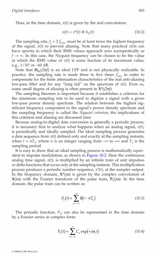
Digital Interfaces 393
Thus, in the time domain, x(t) is given by the real convolution:
x(t) = x*(t) hIL(t) (10.2)
The sampling rate, fs = 2 fmax, must be at least twice the highest frequencyof the signal, x(t) to prevent aliasing. Note that many practical x(t)s canhave spectra in which their RMS values approach zero asymptotically asf Æ . In this case, the Nyquist frequency can be chosen to be the valueat which the RMS value of x(t) is some fraction of its maximum value,e.g., 1/103 or -60 dB.
Note that HIL(j2pf) is an ideal LPF and is not physically realizable. Inpractice, the sampling rate is made three to five times fmax in order tocompensate for the finite attenuation characteristics of the real anti-aliasinglow-pass filter and for any “long tail” on the spectrum of x(t). Even so,some small degree of aliasing is often present in X*(j2pf).
The sampling theorem is important because it establishes a criterion forthe minimum sampling rate to be used to digitize a signal with a givenlow-pass power density spectrum. The relation between the highest sig-nificant frequency component in the signal’s power density spectrum andthe sampling frequency is called the Nyquist criterion; the implications ofthis criterion and aliasing are discussed later.
Because analog-to-digital data conversion is generally a periodic process,it is necessary first to analyze what happens when an analog signal, x(t),is periodically and ideally sampled. The ideal sampling process generatesa data sequence from x(t) defined only and exactly at the sampling instants,when t = nTS, where n is an integer ranging from - to + and TS is thesampling period.
It is easy to show that an ideal sampling process is mathematically equiv-
analog time signal, x(t), is multiplied by an infinite train of unit impulsesor delta functions that occur only at the sampling instants. This multiplicationprocess produces a periodic number sequence, x*(t), at the sampler output.In the frequency domain, X*(jw) is given by the complex convolution ofX(jw) with the Fourier transform of the pulse train, PT(jw). In the timedomain, the pulse train can be written as:
(10.3)
The periodic function, PT, can also be represented in the time domainby a Fourier series in complex form:
(10.4)
P t t nTT Sn
( ) = -( )= -
 d
P t C j tT n sn
( ) = +( )=
 exp–
w
© 2004 by CRC Press LLC
alent to impulse modulation, as shown in Figure 10.2. Here the continuous

394 Analysis and Application of Analog Electronic Circuits
where
(10.5)
and the complex-form Fourier series coefficients are given by the well-known integral:
(10.6)
Thus, the complex Fourier series for the pulse train is found to be:
(10.7)
The sampler output in the time-domain is the product of PT (t) and x(t):
(10.8)
FIGURE 10.2(A) A sampler equivalent of periodic analog-to-digital conversion. (B) An impulse modulatorequivalent to a sampler.
∞
PT (t) = δ(t − nTs)n = −∞
X*(jω) = X(jω) ⊗ PT (jω)X(jω)
Ts
x*(t)x(t)
w ps
ST= 2
r s
CT
P t j t dtTn
ST s
T
T
Ss
s
= ( ) -( ) =-Ú1 1
2
2
exp w
P tT
jn tTS
sn
( ) = +( )=
Â1exp
–
w
x t x tT
jn tS
sn
* exp–
( ) = ( ) +( )=
Â1 w
© 2004 by CRC Press LLC
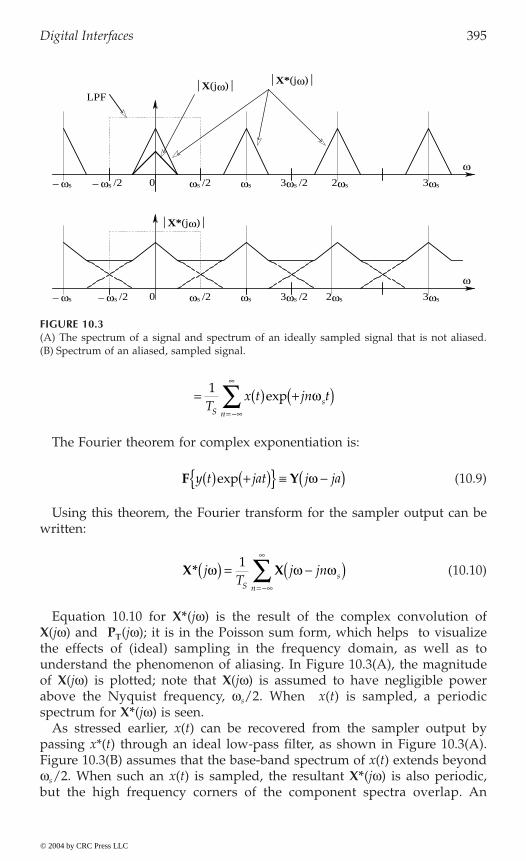
Digital Interfaces 395
The Fourier theorem for complex exponentiation is:
(10.9)
Using this theorem, the Fourier transform for the sampler output can bewritten:
(10.10)
Equation 10.10 for X*(jw) is the result of the complex convolution ofX(jw) and PT(jw); it is in the Poisson sum form, which helps to visualizethe effects of (ideal) sampling in the frequency domain, as well as tounderstand the phenomenon of aliasing. In Figure 10.3(A), the magnitudeof X(jw) is plotted; note that X(jw) is assumed to have negligible powerabove the Nyquist frequency, ws/2. When x(t) is sampled, a periodicspectrum for X*(jw) is seen.
As stressed earlier, x(t) can be recovered from the sampler output bypassing x*(t) through an ideal low-pass filter, as shown in Figure 10.3(A).Figure 10.3(B) assumes that the base-band spectrum of x(t) extends beyondws/2. When such an x(t) is sampled, the resultant X*(jw) is also periodic,but the high frequency corners of the component spectra overlap. An
FIGURE 10.3(A) The spectrum of a signal and spectrum of an ideally sampled signal that is not aliased.(B) Spectrum of an aliased, sampled signal.
0− ωs /2
0− ωs − ωs /2
ωs /2
ωs /2
ωs
ωs
3ωs /2− ωs
3ωs /2
2ωs
2ωs
3ωs
3ωs
ω
ω
LPFX(jω) X*(jω)
X*(jω)
= ( ) +( )=
Â1T
x t jn tS
sn
exp–
w
F Yy t jat j ja( ) +( ) ∫ -( )exp w
X* XjT
j jnS
sn
w w w( ) = -( )=
Â1
–
© 2004 by CRC Press LLC
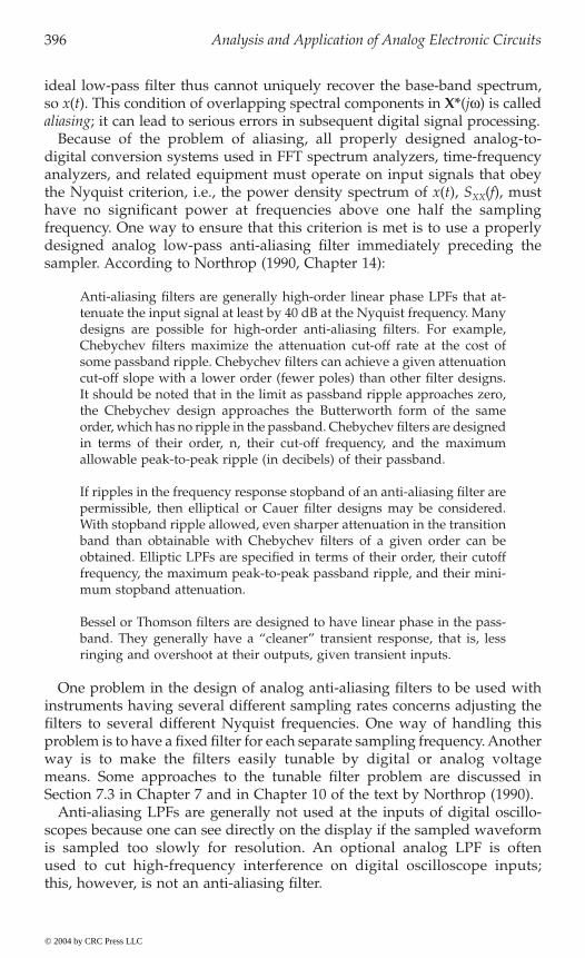
396 Analysis and Application of Analog Electronic Circuits
ideal low-pass filter thus cannot uniquely recover the base-band spectrum,so x(t). This condition of overlapping spectral components in X*(jw) is calledaliasing; it can lead to serious errors in subsequent digital signal processing.
Because of the problem of aliasing, all properly designed analog-to-digital conversion systems used in FFT spectrum analyzers, time-frequencyanalyzers, and related equipment must operate on input signals that obeythe Nyquist criterion, i.e., the power density spectrum of x(t), SXX(f), musthave no significant power at frequencies above one half the samplingfrequency. One way to ensure that this criterion is met is to use a properlydesigned analog low-pass anti-aliasing filter immediately preceding thesampler. According to Northrop (1990, Chapter 14):
Anti-aliasing filters are generally high-order linear phase LPFs that at-tenuate the input signal at least by 40 dB at the Nyquist frequency. Manydesigns are possible for high-order anti-aliasing filters. For example,Chebychev filters maximize the attenuation cut-off rate at the cost ofsome passband ripple. Chebychev filters can achieve a given attenuationcut-off slope with a lower order (fewer poles) than other filter designs.It should be noted that in the limit as passband ripple approaches zero,the Chebychev design approaches the Butterworth form of the sameorder, which has no ripple in the passband. Chebychev filters are designedin terms of their order, n, their cut-off frequency, and the maximumallowable peak-to-peak ripple (in decibels) of their passband.
If ripples in the frequency response stopband of an anti-aliasing filter arepermissible, then elliptical or Cauer filter designs may be considered.With stopband ripple allowed, even sharper attenuation in the transitionband than obtainable with Chebychev filters of a given order can beobtained. Elliptic LPFs are specified in terms of their order, their cutofffrequency, the maximum peak-to-peak passband ripple, and their mini-mum stopband attenuation.
Bessel or Thomson filters are designed to have linear phase in the pass-band. They generally have a “cleaner” transient response, that is, lessringing and overshoot at their outputs, given transient inputs.
One problem in the design of analog anti-aliasing filters to be used withinstruments having several different sampling rates concerns adjusting thefilters to several different Nyquist frequencies. One way of handling thisproblem is to have a fixed filter for each separate sampling frequency. Anotherway is to make the filters easily tunable by digital or analog voltagemeans. Some approaches to the tunable filter problem are discussed inSection 7.3 in Chapter 7 and in Chapter 10 of the text by Northrop (1990).
Anti-aliasing LPFs are generally not used at the inputs of digital oscillo-scopes because one can see directly on the display if the sampled waveformis sampled too slowly for resolution. An optional analog LPF is oftenused to cut high-frequency interference on digital oscilloscope inputs;this, however, is not an anti-aliasing filter.
© 2004 by CRC Press LLC
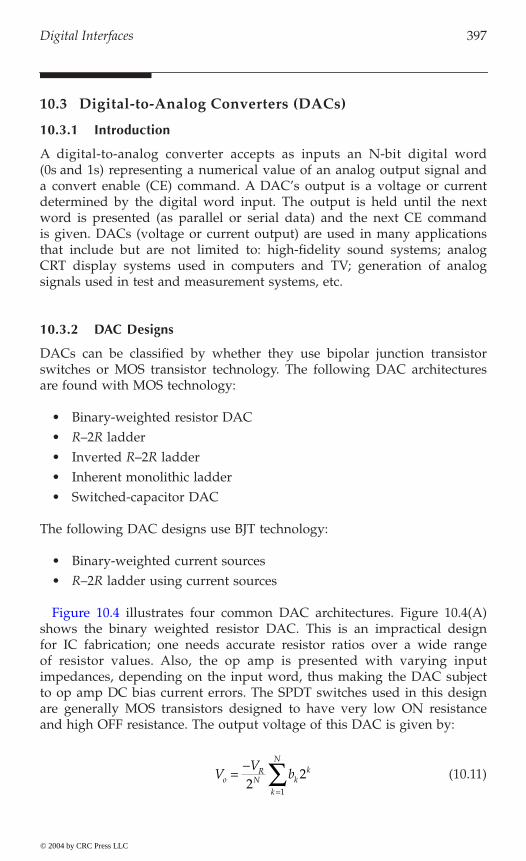
Digital Interfaces 397
10.3 Digital-to-Analog Converters (DACs)
10.3.1 Introduction
A digital-to-analog converter accepts as inputs an N-bit digital word(0s and 1s) representing a numerical value of an analog output signal anda convert enable (CE) command. A DAC’s output is a voltage or currentdetermined by the digital word input. The output is held until the nextword is presented (as parallel or serial data) and the next CE commandis given. DACs (voltage or current output) are used in many applicationsthat include but are not limited to: high-fidelity sound systems; analogCRT display systems used in computers and TV; generation of analogsignals used in test and measurement systems, etc.
10.3.2 DAC Designs
DACs can be classified by whether they use bipolar junction transistorswitches or MOS transistor technology. The following DAC architecturesare found with MOS technology:
• Binary-weighted resistor DAC• R–2R ladder• Inverted R–2R ladder• Inherent monolithic ladder• Switched-capacitor DAC
The following DAC designs use BJT technology:
• Binary-weighted current sources• R–2R ladder using current sources
shows the binary weighted resistor DAC. This is an impractical designfor IC fabrication; one needs accurate resistor ratios over a wide rangeof resistor values. Also, the op amp is presented with varying inputimpedances, depending on the input word, thus making the DAC subjectto op amp DC bias current errors. The SPDT switches used in this designare generally MOS transistors designed to have very low ON resistanceand high OFF resistance. The output voltage of this DAC is given by:
(10.11)VV
boR
N kk
k
N
= -
=Â2
21
© 2004 by CRC Press LLC
Figure 10.4 illustrates four common DAC architectures. Figure 10.4(A)

398 Analysis and Application of Analog Electronic Circuits
where N is the bit length of the binary “word” being converted and bk is “0”or “1,” depending on the word.
Figure 10.4(B) illustrates the popular R–2R ladder DAC. Here only tworesistor values are used; their exact values are not critical, but the ratio must
FIGURE 10.4Four kinds of DAC circuits using op amps: (A) a binary-weighted resistor DAC (not practicalfor N > 8); (B) the R–2R ladder DAC; (C) the inverted R–2R ladder DAC; and (D) a binary-weighted current source DAC (not practical for N > 8).
R
2NR 4R 2R
. . .
. . .
. . .VR
VR
−VR
Vo
Vo
Vo
Vo. . .
. . .
. . .
. . .VR
. . .
. . .
. . .
. . .
. . .
bN b2 b1
0 010 1 1
1 1 10 0 0
2R
2R 2R 2R
R R R R
b1b2bN
bN
2R 2R 2R 2R
RRR
b1 b2
0 0 01 1 1
Io /2N−1Io /2N Io /4 Io /2
bN bN−1 b1b2
1 1 110 0 0 0
R
A
B
C
D
© 2004 by CRC Press LLC
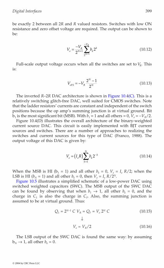
Digital Interfaces 399
be exactly 2 between all 2R and R valued resistors. Switches with low ONresistance and zero offset voltage are required. The output can be shown tobe:
(10.12)
Full-scale output voltage occurs when all the switches are set to VR. Thisis:
(10.13)
relatively switching glitch-free DAC, well suited for CMOS switches. Notethat the ladder resistors’ currents are constant and independent of the switchpositions because the op amp’s summing junction is at virtual ground. Bitb1 is the most significant bit (MSB). With b1 = 1 and all others = 0, Vo = -VR/2.
Figure 10.4(D) illustrates the overall architecture of the binary-weightedcurrent source DAC. This circuit is easily implemented with BJT currentsources and switches. There are a number of approaches to realizing theswitches and current sources for this type of DAC (Franco, 1988). Theoutput voltage of this DAC is given by:
(10.14)
When the MSB is HI (b1 = 1) and all other bk = 0, Vo = Io R/2; when theLSB is HI (bN = 1) and all other bk = 0, then Vo = Io R/2N.
switched weighted capacitors (SWC). The MSB output of the SWC DACcan be found by observing that when b1 Æ 1, all other bk = 0, and thecharge in C1 is also the charge in CF. Also, the summing junction isassumed to be at virtual ground. Thus:
Q1 = 2N-1 C VR = QF = Vo 2N C (10.15)
Ø
Vo = VR/2 (10.16)
The LSB output of the SWC DAC is found the same way: by assumingbN Æ 1, all other bk = 0.
VV
boR
N kk
V
N
R
= -+
-
+Â2
21
2 1
V VoFS R
N
N= - -2 12
V I R bo o kk
k
N
= ( ) -
=Â 2
1
© 2004 by CRC Press LLC
The inverted R–2R DAC architecture is shown in Figure 10.4(C). This is a
Figure 10.5 illustrates a simplified schematic of a low-power DAC using
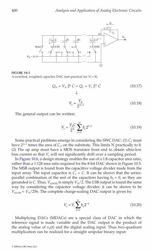
400 Analysis and Application of Analog Electronic Circuits
QN = VR 20 C = QF = Vo 2N C (10.17)
Ø
(10.18)
The general output can be written:
(10.19)
Some practical problems emerge in considering the SWC DAC: (1) C1 musthave 2N-1 times the area of CN on the substrate. This limits N practically to 8.(2) The op amp must have a MOS transistor front end to obtain ultra-lowbias current so that Vo will not significantly drift over a sampling period.
rather than a 1:128 area ratio required for the 8-bit DAC shown in Figure 10.5.The MSB output is found from the capacitive voltage divider made from theinput array. The input capacitor is C1 = C. It can be shown that the series-parallel combination of the rest of the capacitors having bk = 0, so they aregrounded is C. Thus, Vo(MSB) is simply VR/2. The LSB output is found the sameway by considering the capacitor voltage divider; it can be shown to beVo(LSB) = VR/256. The complete charge-scaling DAC output is given by:
(10.20)
Multiplying DACs (MDACs) are a special class of DAC in which thereference signal is made variable and the DAC output is the product ofthe analog value of vR(t) and the digital scaling input. Thus two-quadrantmultiplication can be realized for a straight unipolar binary input:
FIGURE 10.5A switched, weighted capacitor DAC (not practical for N > 8).
Vo
(LSB) b1 (MSB)bN bN−2
C 2N
C 2N −1
. . .
. . . (0)
2C 4CC
. . .
00 01 1 1 1
CF
C1CN
0
Reset
VR < 0
QF
VV
oR
N= -2 1
VV C
boRN k
k
k
N
= -
=Â2
2 1
1
V V bo r kk
k
N
= -
=Â 2
1
© 2004 by CRC Press LLC
In Figure 10.6, a design strategy enables the use of a 1:8 capacitor area ratio,

Digital Interfaces 401
(10.21)
If the DAC is set up for bipolar offset binary (BOB) operation, true four-quadrant multiplication occurs. The output of a DAC configured for BOB,such as the AD7845 12-bit MDAC, is given by:
(10.22)
For N = 12:
(10.23A)
(10.23B)
(10.23C)
(10.23D)
(10.23E)
MDACs find application in waveform generation; digitally controlledattenuators; programmable power supplies; programmable gain amplifiers;
FIGURE 10.6A charge-scaling switched-capacitor DAC.
b1 (MSB)b2b3b4b5b6b7b8Reset
C/8
C/8 C /8 C/4C/4 C/2 C/2C C
0 0 0 0 0 0 0 01 1 1 1 1 1 1 1
2C/15
VR
Vo
(LSB)
MSB arrayLSB array
v t v to RN k
k
N
( ) = ( )È
ÎÍÍ
ù
ûúú
-
=Â2 2
1
v t v t bo R N kk
k
N
( ) = ( ) - +È
ÎÍÍ
ù
ûúú-
-
=Â1
12
211
1
b V v tk o R = = ( )1111 1111 111120472048
,
b V v tk o R = = ( )1000 0000 00011
2048 ,
b V v tk o R = = ( ) =1000 0000 00010
20480 ,
b V v tk o R = = - ( )0111 1111 11111
2048 ,
b V v t v tk o R R = = - ( ) = - ( )0000 0000 000020482048
,
© 2004 by CRC Press LLC
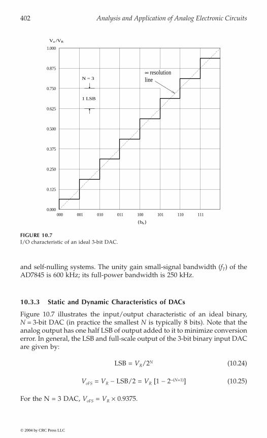
402 Analysis and Application of Analog Electronic Circuits
and self-nulling systems. The unity gain small-signal bandwidth (fT) of theAD7845 is 600 kHz; its full-power bandwidth is 250 kHz.
10.3.3 Static and Dynamic Characteristics of DACs
Figure 10.7 illustrates the input/output characteristic of an ideal binary,N = 3-bit DAC (in practice the smallest N is typically 8 bits). Note that theanalog output has one half LSB of output added to it to minimize conversionerror. In general, the LSB and full-scale output of the 3-bit binary input DACare given by:
LSB = VR/2N (10.24)
VoFS = VR - LSB/2 = VR [1 - 2-(N+1)] (10.25)
For the N = 3 DAC, VoFS = VR ¥ 0.9375.
FIGURE 10.7I/O characteristic of an ideal 3-bit DAC.
111110101100011010001000
1.000
0.750
0.625
0.500
0.375
0.250
0.125
0.000
Vo /VR
bk
1 LSB
N = 3
0.875∞ resolutionline
© 2004 by CRC Press LLC
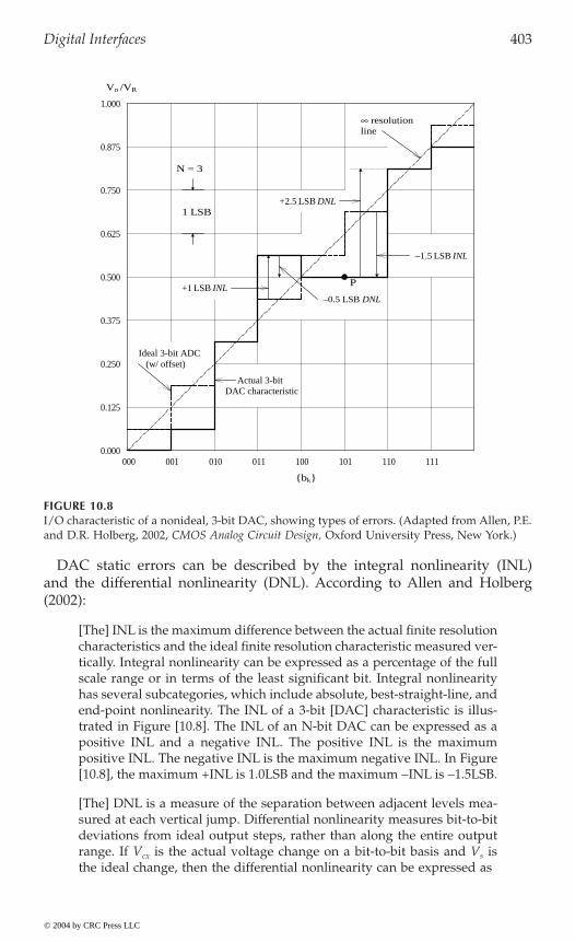
Digital Interfaces 403
DAC static errors can be described by the integral nonlinearity (INL)and the differential nonlinearity (DNL). According to Allen and Holberg(2002):
[The] INL is the maximum difference between the actual finite resolutioncharacteristics and the ideal finite resolution characteristic measured ver-tically. Integral nonlinearity can be expressed as a percentage of the fullscale range or in terms of the least significant bit. Integral nonlinearityhas several subcategories, which include absolute, best-straight-line, andend-point nonlinearity. The INL of a 3-bit [DAC] characteristic is illus-trated in Figure [10.8]. The INL of an N-bit DAC can be expressed as apositive INL and a negative INL. The positive INL is the maximumpositive INL. The negative INL is the maximum negative INL. In Figure[10.8], the maximum +INL is 1.0LSB and the maximum -INL is -1.5LSB.
[The] DNL is a measure of the separation between adjacent levels mea-sured at each vertical jump. Differential nonlinearity measures bit-to-bitdeviations from ideal output steps, rather than along the entire outputrange. If Vcx is the actual voltage change on a bit-to-bit basis and Vs isthe ideal change, then the differential nonlinearity can be expressed as
FIGURE 10.8I/O characteristic of a nonideal, 3-bit DAC, showing types of errors. (Adapted from Allen, P.E.and D.R. Holberg, 2002, CMOS Analog Circuit Design, Oxford University Press, New York.)
111110101100011010001000
0.750
0.625
0.500
0.375
0.250
0.125
0.000
Vo /VR
bk
N = 3
0.875
Actual 3-bitDAC characteristic
P
1 LSB+2.5 LSB DNL
1.000
−1.5 LSB INL
Ideal 3-bit ADC(w/ offset)
∞ resolutionline
−0.5 LSB DNL+1 LSB INL
© 2004 by CRC Press LLC

404 Analysis and Application of Analog Electronic Circuits
[10.26]
For an N-bit DAC and a full-scale voltage range of VFSR,
[10.27]
measure of the step size and is totally independent of how far the actualstep change may be from the infinite resolution characteristic at the jump.The change from 101 to 110 results in a maximum +DNL of 2.5LSBs(Vcx/Vs = 2.5LSBs). The maximum negative DNL is found when thedigital input code changes from 011 to 100. The change is -0.5 LSB(Vcx/Vs = -0.5LSB), which gives a DNL of -0.5LSB. It is of interest to notethat as the digital input code changes from 100 to 101, no change occurs(point P). Because we know that a change should have occurred, we cansay that the DNL at point P is -0.5LSB.
Dynamic DAC characteristics of DACs limit the speed at which theycan convert digital words to analog signals. If a DAC IC has an on-chipop amp for current-to-voltage conversion, the op amp’s fT and slew rate,h, provide one factor that limits conversion speed. Another factor comesfrom on-chip parasitic capacitances that shunt all resistors and transistorsto substrate ground. Conversion speed is also limited by the rate at whichMOS and/or BJT switches can turn on and off. Glitches — unwanted(artifactual) transients on the DAC output immediately following a digitalword input — are another problem with high-speed DACs. Franco (1988)describes their origin and a cure:
… these are due to the internal circuitry’s nonuniform response to inputbit changes and to poor synchronization of the bit changes themselves.For instance, if during the center-scale transition from 011…1 to 100…0the MSB is perceived as going on before (after) all other bits go off, theoutput will momentarily [try to] swing to full-scale (to zero), thus causingan output glitch.
Glitches are of particular concern in CRT display applications. Filteringdoesn’t solve the problem since the area under the glitch is integratedand carried over subsequent steps [i.e., as the filter’s impulse response],which will therefore also be in error. Glitches can be minimized eitherby synchronizing the input bit changes with a high-speed parallel latchregister, or by processing the DAC output with a[n] S/H [sample andhold] deglitcher circuit. The circuit is switched to hold mode just priorto the input code change and is returned to the track mode only afterthe DAC gas settle[s] to its new level, thus preventing any glitches fromreaching the output.
DNL LSBs=-
¥ = -( )V VV
V Vcx s
scx s100 1%
V Vs FSRN= 2
© 2004 by CRC Press LLC
Figure [10.8] also illustrates differential nonlinearity. Note that DNL is a

Digital Interfaces 405
The fast video DACs available in 2003 can convert at approximately 200MSPS. For example the 10-bit, Analog Devices AD9732 DAC is rated at200 MSPS and takes 5 ns to settle to one half LSB. The Faraday 8-bitDAC8001 also is rated at 200 MSPS and claims a 4-ns analog settling time.
10.4 Hold Circuits
Just as the sampling process can be interpreted in the frequency domain,so can the process of sample (or track) and hold of analog signals froma DAC. Note that the digital input to a DAC is generally periodic withperiod Ts. The DAC’s analog output from the nth digital input is generallyheld constant until the (n + 1)th input updates it. This process generates astepwise output waveform if bk is changing and can be viewed as linearfiltering operation. The impulse response of the zero-order hold (ZOH)filter to a unit input word at t = 0, and zero inputs at sampling instantsthereafter is:
ho(t) = U(t) - U(t - Ts) (10.28)
where U(t) is the unit step function, defined as zero for all negativeargument, and 1 for all positive argument. ho(t) is thus a pulse of unitheight and duration (0, Ts), else zero. The Laplace transform of ho(t) is:
(10.29)
To find the frequency response of the ZOH, let s Æ jw and use the Eulerrelation for ejq. The ZOH’s frequency response is easily shown to be:
(10.30)
Note that the zeros in Ho(jw) occur at w = n2p/Ts r/s, where n = 1, 2,3, …, and 2p/Ts is the radian sampling frequency of the system. Thus,the overall process of sampling an analog signal, x(t), and reconvertingto (held) analog form by a DAC can be written in the frequency domain(neglecting quantization) as (Northrop, 1990):
(10.31)
H ss s
eeso
sTsT
ss
( ) = - = ---1 1 1
Ho ss
s
j Tj TT
Te sw
ww
w( ) = ( )( )
-sin 22
2
X XjT
Tj jn es
sns
j Tsww
ww w w( ) = ( )
( ) -( )=
 sin 22
0
2
© 2004 by CRC Press LLC

406 Analysis and Application of Analog Electronic Circuits
Note that other more sophisticated holds exist; their realization is at theexpense of some circuit complexity, however. For example, the first-difference extrapolator hold that generates linear slope transitions betweensampling instants (instead of steps) can be realized with three DACs, aresettable analog integrator, and an analog adder (Northrop, 1990). Itstransfer function can be shown to be:
(10.32)
10.5 Analog-to-Digital Converters (ADCs)
10.5.1 Introduction
Although the technology for DACs is relatively simple, there are manydiverse kinds of ADCs and ADC algorithms. The five major categories ofADC are:
1. Tracking (servo) converters2. Successive approximation converters3. Integrating converters4. Flash (parallel) converters5. Oversampled (sigma–delta) converters
Next, each category will be examined and a description of how it worksgiven.
Note that an infinite-resolution analog signal, x(t), is quantized into eight 3-
malized quantization error, (NQE) ∫ ve/LSB, of this converter; the quantiza-tion error voltage is given by:
(10.33)
Note that the NQE is bounded by plus or minus one half LSB except forvx/VFS ≥ 7/8, where it reaches +1 LSB at vx/VFS = 1. 1 LSB = VFS/23 =VFS/8 for this 3-bit ADC.
H ses
e es
e e
se
sT sT sT sT sT
( ) = - + - + --( )- - - - -
1 1 2 12
2
v v V b v V b b b Nc x FS kk
k
N
x FS= - = - + +( ) =-
=
- - -Â 2 2 2 2 31
11
22
33 , . for
© 2004 by CRC Press LLC
Figure 10.9 shows the transfer characteristic of a 3-bit binary-output ADC.
bit binary words, depending on its value. Figure 10.10 illustrates the nor-

Digital Interfaces 407
10.5.2 The Tracking (Servo) ADC
The first ADC considered is the tracking (servo) ADC, aka the counting
version is initiated, the up/down counter is reset and then counts up. Theup/down counter’s digital output goes to a DAC. The DAC’s voltage outputramps up at a rate easily shown to be:
(10.34)
where N is the number of bits of the DAC and U/D counter and Tc is theclock period.
VoFS is generally made equal to Vxmax. If N = 10 bits, Tc = 5 ¥ 10-7 sec (fc =2 MHz), and Vomax = 10 V, then the Vo slew rate is h = 1.953 ¥ 104 V/sec.By resetting the counter following each 10-V conversion, approximately1,950 10-V conversions can be made per second. If conversion is not stopped-when the comparator output goes LO (Vo > Vx) and the counter is not reset,then the counter will increment down by 1 LSB at the next clock cycle,
FIGURE 10.9Transfer characteristic of an ideal 3-bit binary-output ADC.
1 LSB
∞ resolutionline
000
001
010
011
100
101
110
111
bk
0.000 0.125 0.250 0.375 0.500 0.625 0.750 0.875 1.000
3-bit binaryoutput code
vx /VFS
(Normalized input voltage)
h = ( )V T VoFSN
c2 sec
© 2004 by CRC Press LLC
ADC. A block diagram for this ADC is shown in Figure 10.11. When con-

408 Analysis and Application of Analog Electronic Circuits
causing Vo to decrease by 1 LSB, thus bringing Vo < Vx; the comparator thengoes HI and the next clock pulse increments the counter up, so Vo thenexceeds Vx. The process repeats cyclically, generating a steady-state 1-LSBdither in the digital output.
When this ADC is used in the tracking mode to improve conversionspeed, the LSB output is not used in order to avoid the steady-state dither.If the ADC is reset after each conversion, the end of conversion (EOC)signal occurs when Vo > Vx by 1 LSB the first time after conversion isinitiated. Although this mode of operation avoids dither, it is slower andstill has a conversion error between 0 and +1 LSB.
The servo counting ADC is well suited for data conversion of DC orlow-frequency AC signals. It is also easy to implement in hardware (ICs).One disadvantage is that conversion time depends on the value of vx/Vxmax,i.e., it is variable. Another disadvantage is the LSB dither seen in thesteady-state tracking mode.
10.5.3 The Successive Approximation ADC
Like the servo counting ADC, the successive approximation ADC(SAADC) uses a comparator and a DAC in a closed-loop architecture, as
a start signal from the controlling computer’s I/O interface at t = nT. Startcauses the analog input signal, Vx, to be held at [Vx(nT)] and the counter’s
FIGURE 10.10Normalized quantization error vs. input voltage for an ideal 3-bit binary ADC.
0.000 0.125 0.250 0.375 0.500 0.625 0.750 0.875 1.000
Vo /VFS
Input voltage
0
0.5
1.0
1.5
L SB
− 0.5
− 1.5
− 1.0
Quantizationerror (LSB)
© 2004 by CRC Press LLC
shown in Figure 10.12. The conversion cycle for a 10-bit SAADC begins with
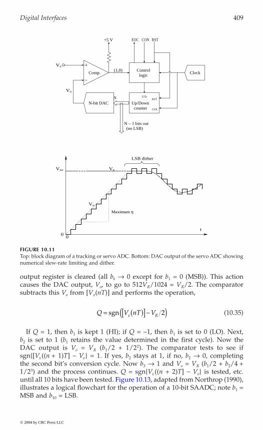
Digital Interfaces 409
output register is cleared (all bk Æ 0 except for b1 = 0 (MSB)). This actioncauses the DAC output, Vo, to go to 512VR/1024 = VR/2. The comparatorsubtracts this Vo from [Vx(nT)] and performs the operation,
(10.35)
If Q = 1, then b1 is kept 1 (HI); if Q = -1, then b1 is set to 0 (LO). Next,b2 is set to 1 (b1 retains the value determined in the first cycle). Now theDAC output is Vo = VR (b1/2 + 1/22). The comparator tests to see ifsgn[Vx((n + 1)T] - Vo = 1. If yes, b2 stays at 1, if no, b2 Æ 0, completingthe second bit’s conversion cycle. Now b3 Æ 1 and Vo = VR (b1/2 + b2/4 +1/23) and the process continues. Q = sgnVx((n + 2)T] - Vo is tested, etc.
illustrates a logical flowchart for the operation of a 10-bit SAADC; note b1 =MSB and b10 = LSB.
FIGURE 10.11Top: block diagram of a tracking or servo ADC. Bottom: DAC output of the servo ADC showingnumerical slew-rate limiting and dither.
t
Vo
Vo
00
ClockControl
logicComp.
+5 V EOC RSTCON
CLK
RSTU/DN
N − 1 bits out(no LSB)
VxVxo
LSB dither
Vx
(1,0)
N-bit DAC Up/Downcounter
Maximum η
Q V nT Vx R= ( )[ ] -( )sgn 2
© 2004 by CRC Press LLC
until all 10 bits have been tested. Figure 10.13, adapted from Northrop (1990),
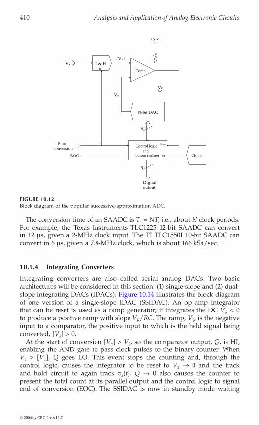
410 Analysis and Application of Analog Electronic Circuits
The conversion time of an SAADC is Tc = NT, i.e., about N clock periods.For example, the Texas Instruments TLC1225 12-bit SAADC can convertin 12 ms, given a 2-MHz clock input. The TI TLC1550I 10-bit SAADC canconvert in 6 ms, given a 7.8-MHz clock, which is about 166 kSa/sec.
10.5.4 Integrating Converters
Integrating converters are also called serial analog DACs. Two basicarchitectures will be considered in this section: (1) single-slope and (2) dual-
of one version of a single-slope IDAC (SSIDAC). An op amp integratorthat can be reset is used as a ramp generator; it integrates the DC VR < 0to produce a positive ramp with slope VR/RC. The ramp, V2, is the negativeinput to a comparator, the positive input to which is the held signal beingconverted, [Vx] > 0.
At the start of conversion [Vx] > V2, so the comparator output, Q, is HI,enabling the AND gate to pass clock pulses to the binary counter. WhenV2 > [Vx], Q goes LO. This event stops the counting and, through thecontrol logic, causes the integrator to be reset to V2 Æ 0 and the trackand hold circuit to again track vx(t). Q Æ 0 also causes the counter topresent the total count at its parallel output and the control logic to signalend of conversion (EOC). The SSIDAC is now in standby mode waiting
FIGURE 10.12Block diagram of the popular successive-approximation ADC.
Comp.
N-bit DAC
VR
Vo
Vx
+5 V
N
N
T & HH
Status
[Vx]
Control logicand
output register ClockEOC CP
Startconversion
Digitaloutput
© 2004 by CRC Press LLC
slope integrating DACs (IDACs). Figure 10.14 illustrates the block diagram

Digital Interfaces 411
FIGURE 10.13Logical flowchart illustrating the steps in one conversion cycle of a successive-approximationADC.
FIGURE 10.14Block diagram of a single-slope integrating ADC.
Sample & holdVx at t = 0
Clear outputregister (all bk = 0)
Set b1 = 1(MSB HI)
Set k = 1 inbit counter
Is Vx > Vo?Yes
Leave bk = 1
No
Set bk = 0
Do EOC outLatch data out
Standby for next start
YesNo
Start
(Continue)Increment counter
k’ = k + 1
Is k’ = 11?Set bk’ = 1
vx(t)[Vx]j
VR
T & H
+
−
Outputcounter
bk
C
T/H
R
Clock
Convert
OA
Controllogic
EOC
CON
CP
RSTQComp.
CP
© 2004 by CRC Press LLC
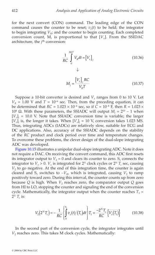
412 Analysis and Application of Analog Electronic Circuits
for the next convert (CON) command. The leading edge of the CONcommand causes the counter to be reset; vx(t) to be held; the integratorto begin integrating VR; and the counter to begin counting. Each completedconversion count, M, is proportional to that [Vx]. From the SSIDACarchitecture, the jth conversion:
(10.36)
Ø
(10.37)
Suppose a 10-bit converter is desired and Vx ranges from 0 to 10 V. LetVR = 1.00 V and T = 10-6 sec. Then, from the preceding equation, it canbe determined that RC = 1.023 ¥ 10-4 sec, so if C = 10-8 F, then R = 1.023 ¥104 W. With these parameters, the SSIADC will output Mj = 210 – 1 when[Vx]j = 10.0 V. Note that SSIADC conversion time is variable; the larger[Vx]j is, the longer it takes. When [Vx]j = 10 V, conversion takes 1.023 MS.Thus, integrating ADCs (IADCs) are relatively slow, suitable for ECG andDC applications. Also, accuracy of the SSIADC depends on the stabilityof the RC product and clock period over time and temperature changes.To overcome these problems, the clever design of the dual-slope integratingADC was developed.
not require a DAC. On receiving the convert command, this ADC first resetsits integrator output to V2 = 0 and clears its counter to zero. S1 connects theintegrator to Vx > 0. Vx is integrated for 2N clock cycles or 2N Tc sec, causingV2 to go negative. At the end of this integration time, the counter is againcleared and S1 switches to -VR, which is integrated, causing V2 to ramppositively toward zero. During this interval, the counter counts up from zerobecause Q is high. When V2 reaches zero, the comparator output Q goesfrom HI to LO, stopping the counter and signaling the end of the conversioncycle. Mathematically, the integrator output when the counter reaches T1 =2N Tc is:
(10.38)
In the second part of the conversion cycle, the integrator integrates untilV2 reaches zero. This takes M clock cycles. Mathematically:
1
0RC
V dt VR
MjT
x jÚ = [ ]
MV RC
V Tj
x j
R
=[ ]
V TRC
v t T dt TT
RCV TN
c x
TN
cx2 1
0
1 121 2
1
( ) = - ( ) ( )ÏÌÔ
ÓÔ
¸ýÔ
þÔ=
- ( ) Ú
© 2004 by CRC Press LLC
Figure 10.15 illustrates a unipolar dual-slope integrating ADC. Note it does
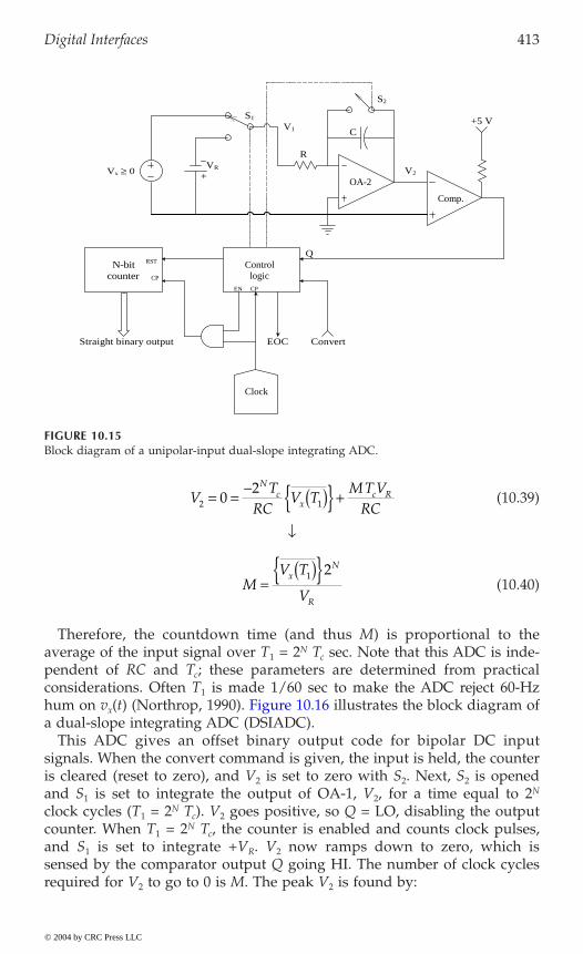
Digital Interfaces 413
(10.39)
Ø
(10.40)
Therefore, the countdown time (and thus M) is proportional to theaverage of the input signal over T1 = 2N Tc sec. Note that this ADC is inde-pendent of RC and Tc; these parameters are determined from practicalconsiderations. Often T1 is made 1/60 sec to make the ADC reject 60-Hz
x
a dual-slope integrating ADC (DSIADC).This ADC gives an offset binary output code for bipolar DC input
signals. When the convert command is given, the input is held, the counteris cleared (reset to zero), and V2 is set to zero with S2. Next, S2 is openedand S1 is set to integrate the output of OA-1, V2, for a time equal to 2N
clock cycles (T1 = 2N Tc). V2 goes positive, so Q = LO, disabling the outputcounter. When T1 = 2N Tc, the counter is enabled and counts clock pulses,and S1 is set to integrate +VR. V2 now ramps down to zero, which issensed by the comparator output Q going HI. The number of clock cyclesrequired for V2 to go to 0 is M. The peak V2 is found by:
FIGURE 10.15Block diagram of a unipolar-input dual-slope integrating ADC.
R
C
Comp.
OA-2
EOC Convert
Controllogic
N-bitcounter
S2
RSTQ
S1 +5 V
Clock
EN
V2
CP
CP
V1
VR
Straight binary output
Vx ≥ 0 +
−
VT
RCV T
MT VRC
Nc
xc R
2 102
= =- ( ) +
MV T
Vx
N
R
=( ) 1 2
© 2004 by CRC Press LLC
hum on v (t) (Northrop, 1990). Figure 10.16 illustrates the block diagram of

414 Analysis and Application of Analog Electronic Circuits
(10.41)
The number of clock cycles required to integrate V2(2N Tc) to zero is M:
(10.42)
Solving for M:
(10.43)
Note that when [Vx] = -VR, M = 0, when [Vx] = 0, M = 2N-1 (1 MSB), andwhen [Vx] = +VR, M = 2N, giving a true offset binary output code. Note thatthis dual-slope integrating ADC also has accuracy independent of RC and Tc.
10.5.5 Flash Converters
The fastest ADCs are flash converters (FADCs) that enable signal samplingin the ns range and thus are widely used in medical ultrasound systems,
FIGURE 10.16Block diagram of a bipolar-input dual-slope integrating ADC. The output is in offset binary code.
VxVR
R R
C
Comp.
OA-1 OA-2
EOC Convert
Controllogic
N-bitcounter
S2
RSTQ
Offset binary output
S1 +5 V
Clock
EN
V2
CP
CP
V1R R/2
V TRC
V V dtV T
RC
V T
RCN
c R x
T
RN
c xN
c
Nc
2
0
2
21
22
22
2( ) = + [ ]( ) = + [ ]Ú
V TRC
V T
RCV MT
RCR
Nc x
Nc R c2
22
20+ [ ] - =
M V VNx R= + [ ]( )-2 11
© 2004 by CRC Press LLC
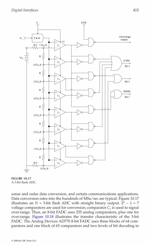
Digital Interfaces 415
sonar and radar data conversion, and certain communications applications.Data conversion rates into the hundreds of MSa/sec are typical. Figure 10.17illustrates an N = 3-bit flash ADC with straight binary output. 2N - 1 = 7voltage comparators are used for conversion; comparator C1 is used to signalover-range. Thus, an 8-bit FADC uses 255 analog comparators, plus one for
FADC. The Analog Devices AD770 8-bit FADC uses three blocks of 64 com-parators and one block of 65 comparators and two levels of bit decoding to
FIGURE 10.17A 3-bit flash ADC.
Overrangeoutput
(LSB)
Bit 3
Bit 2
(MSB)
Bit 1
T & HVx
VRR
R
R
R
R
R
R
R/2
R/2
EXPS
C1
C2
C3
C4
C5
C8
C7
C6
0.5VR /8
1.5VR /8
2.5VR /8
3.5VR /8
4.5VR /8
5.5VR /8
6.5VR /8
7.5VR /8
STB
© 2004 by CRC Press LLC
over-range. Figure 10.18 illustrates the transfer characteristic of the 3-bit
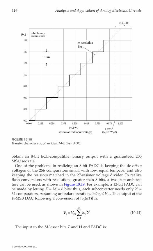
416 Analysis and Application of Analog Electronic Circuits
obtain an 8-bit ECL-compatible, binary output with a guaranteed 200MSa/sec rate.
One of the problems in realizing an 8-bit FADC is keeping the dc offsetvoltages of the 256 comparators small, with low, equal tempcos, and alsokeeping the resistors matched in the 2N-resistor voltage divider. To realizeflash conversions with resolutions greater than 8 bits, a two-step architec-
be made by letting K = M = 6 bits; thus, each subconverter needs only 26 =64 comparators. Assuming unipolar operation, 0 £ vx £ VFS. The output of theK-MSB DAC following a conversion of [vx(nT)] is:
(10.44)
The input to the M-lesser bits T and H and FADC is:
FIGURE 10.18Transfer characteristic of an ideal 3-bit flash ADC.
1 LSB
∞ resolutionline
000
001
010
011
100
101
110
111
bk
0.000 0.125 0.250 0.375 0.500 0.625 0.750 0.875 1.000
3-bit binaryoutput code
0.9375[vx]/VR
O.R. = HI
(Normalized input voltage) ([vx] =7.5VR /8)
V V bFS ii
i
K
11
2==
Â
© 2004 by CRC Press LLC
ture can be used, as shown in Figure 10.19. For example, a 12-bit FADC can
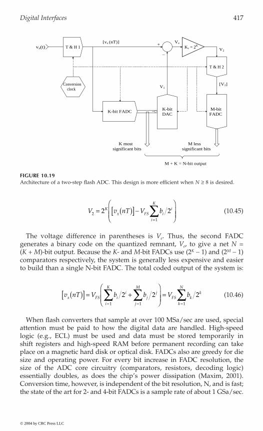
Digital Interfaces 417
(10.45)
The voltage difference in parentheses is Ve. Thus, the second FADCgenerates a binary code on the quantized remnant, Ve, to give a net N =(K + M)-bit output. Because the K- and M-bit FADCs use (2K - 1) and (2M - 1)comparators respectively, the system is generally less expensive and easierto build than a single N-bit FADC. The total coded output of the system is:
(10.46)
When flash converters that sample at over 100 MSa/sec are used, specialattention must be paid to how the digital data are handled. High-speedlogic (e.g., ECL) must be used and data must be stored temporarily inshift registers and high-speed RAM before permanent recording can takeplace on a magnetic hard disk or optical disk. FADCs also are greedy for diesize and operating power. For every bit increase in FADC resolution, thesize of the ADC core circuitry (comparators, resistors, decoding logic)essentially doubles, as does the chip’s power dissipation (Maxim, 2001).Conversion time, however, is independent of the bit resolution, N, and is fast;the state of the art for 2- and 4-bit FADCs is a sample rate of about 1 GSa/sec.
FIGURE 10.19Architecture of a two-step flash ADC. This design is more efficient when N ≥ 8 is desired.
T & H 1 Kv = 2K
T & H 2
M-bitFADC
K-bitDAC
K-bit FADC
Conversionclock
[vx (nT)]
−
+Ve
V2
[V2]
K mostsignificant bits
M lesssignificant bits
M + K = N-bit output
V1
vx(t)
V v nT V bKx FS i
i
i
K
21
2 2= ( )[ ] -Ê
ËÁÁ
¯
=Â
v nT V b b V bx FS ii
i
K
jj
j
M
FS kk
k
N
( )[ ] = +Ê
ËÁÁ
¯ =
= = =Â Â Â2 2 2
1 1 1
© 2004 by CRC Press LLC
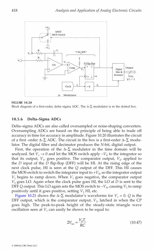
418 Analysis and Application of Analog Electronic Circuits
10.5.6 Delta–Sigma ADCs
Delta–sigma ADCs are also called oversampled or noise-shaping converters.Oversampling ADCs are based on the principle of being able to trade offaccuracy in time for accuracy in amplitude. Figure 10.20 illustrates the circuitof a first -order D–Â ADC. The circuit in the box is a first-order D–Â modu-lator. The digital filter and decimator produces the N-bit, digital output.
First, the operation of the D–Â modulator in the time domain will beanalyzed. Set Vx Æ 0 and let the MOS switch apply -VR to the integrator sothat its output, V1, goes positive. The comparator output, V2, applied tothe D input of the D flip-flop (DFF) will be HI. At the rising edge of thenext clock pulse, HI is seen at the Q output of the DFF. This HI causesthe MOS switch to switch the integrator input to +VR, so the integrator outputV1 begins to ramp down. When V1 goes negative, the comparator outputV2 goes LO. Again when the clock pulse goes HI, the LO at D is sent to theDFF Q output. This LO again sets the MOS switch to -VR, causing V2 to ramppositively until it goes positive, setting V2 HI, etc.
x
DFF output, which is the comparator output, V2, latched in when the CPgoes high. The peak-to-peak height of the steady-state triangle waveoscillation seen at V1 can easily be shown to be equal to:
(10.47)
FIGURE 10.20Block diagram of a first-order, delta–sigma ADC. The D–Â modulator is in the dotted box.
D Flip-flopOA
R
Clock
V1
fc
C“1-bit ADC”
_
Q
Vs
R
SPDTMOS Switch
+VR
−VR
÷ Kfo
CP N bits@ fo << fc
QDComp. V2Output
Digitalfilter &
decimator
∆- Modulator
Vx
2 1VV TRCm
R c=
© 2004 by CRC Press LLC
Figure 10.21 shows the D–Â modulator’s waveforms for V = 0. Q is the

Digital Interfaces 419
where Tc is the DSDAC’s clock period and the other parameters are givenin the figure. The average value of Vs = 0.
Now set Vx = +VR/4 and examine the D–Â ADC’s waveforms (refer to1
Vx and Vs = +VR. Initially, the integrator output V1 ramps negative as v1(t) =-[5VR/(4RC)] t. At the first positive-going clock wave, the LO comparatoroutput, V2, is latched to the DFF’s Q output, setting it low. When Q goeslow, the MOS switch makes Vs = -VR. Now the integrator output rampsupward with slope +3VR/(4RC). When V1 goes positive, the second positiveclock transition latches the HI V2 to Q, setting Vs to +VR. Now theintegrator output, V1, ramps down again with slope -5VR/(4RC).
FIGURE 10.21Waveforms in a first-order D–Â modulator when Vx = 0.
CP
V2
V1
−VR
0
+VR
Vs
Q
t
t
t
t
t
V1m
−V1m
0
0
0
0
Tc
Tc
Tc
Tc
Tc
© 2004 by CRC Press LLC
Figure 10.22). Let the system start with V = 0 at t = 0 and begin to integrate
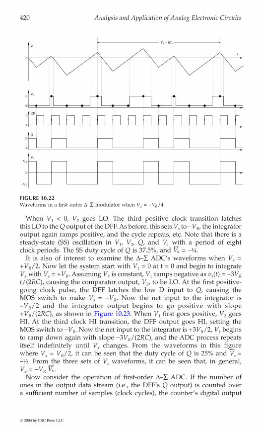
420 Analysis and Application of Analog Electronic Circuits
When V1 < 0, V2 goes LO. The third positive clock transition latchesthis LO to the Q output of the DFF. As before, this sets Vs to -VR, the integratoroutput again ramps positive, and the cycle repeats, etc. Note that there is asteady-state (SS) oscillation in V1, V2, Q, and Vs with a period of eightclock periods. The SS duty cycle of Q is 37.5%, and = -¼.
It is also of interest to examine the D–Â ADC’s waveforms when Vx =+VR/2. Now let the system start with V1 = 0 at t = 0 and begin to integrateVx with Vs = +VR. Assuming Vx is constant, V1 ramps negative as v1(t) = -3VR
t/(2RC), causing the comparator output, V2, to be LO. At the first positive-going clock pulse, the DFF latches the low D input to Q, causing theMOS switch to make Vs = -VR. Now the net input to the integrator is–VR/2 and the integrator output begins to go positive with slope
R 1 2
HI. At the third clock HI transition, the DFF output goes HI, setting theMOS switch to -VR. Now the net input to the integrator is +3VR/2, V1 beginsto ramp down again with slope -3VR/(2RC), and the ADC process repeatsitself indefinitely until Vx changes. From the waveforms in this figurewhere Vx = VR/2, it can be seen that the duty cycle of Q is 25% and Vs =–½. From the three sets of Vs waveforms, it can be seen that, in general,Vx = -VR .
Now consider the operation of first-order D–Â ADC. If the number ofones in the output data stream (i.e., the DFF’s Q output) is counted overa sufficient number of samples (clock cycles), the counter’s digital output
FIGURE 10.22Waveforms in a first-order D–Â modulator when Vx = +VR/4.
t
CP
V1
V2
Q
Vs
0
0
VR
−VR
HI
LO
LO
LO
HI
HI
T1 = 8Tc
Vs
Vs
© 2004 by CRC Press LLC
+V /(2RC), as shown in Figure 10.23. When V first goes positive, V goes
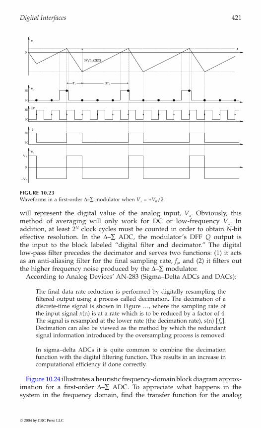
Digital Interfaces 421
will represent the digital value of the analog input, Vx. Obviously, thismethod of averaging will only work for DC or low-frequency Vx. Inaddition, at least 2N clock cycles must be counted in order to obtain N-biteffective resolution. In the D–Â ADC, the modulator’s DFF Q output isthe input to the block labeled “digital filter and decimator.” The digitallow-pass filter precedes the decimator and serves two functions: (1) it actsas an anti-aliasing filter for the final sampling rate, fo, and (2) it filters outthe higher frequency noise produced by the D–Â modulator.
According to Analog Devices’ AN-283 (Sigma–Delta ADCs and DACs):
The final data rate reduction is performed by digitally resampling thefiltered output using a process called decimation. The decimation of adiscrete-time signal is shown in Figure …, where the sampling rate ofthe input signal x(n) is at a rate which is to be reduced by a factor of 4.The signal is resampled at the lower rate (the decimation rate), s(n) [ fo].Decimation can also be viewed as the method by which the redundantsignal information introduced by the oversampling process is removed.
In sigma–delta ADCs it is quite common to combine the decimationfunction with the digital filtering function. This results in an increase incomputational efficiency if done correctly.
imation for a first-order D–Â ADC. To appreciate what happens in thesystem in the frequency domain, find the transfer function for the analog
FIGURE 10.23Waveforms in a first-order D–Â modulator when Vx = +VR/2.
CP
V1
V2
Q
Vs
0
0
VR
−VR
HI
LO
LO
LO
HI
HI
t
3TcTc
3VRTc /(2RC)
© 2004 by CRC Press LLC
Figure 10.24 illustrates a heuristic frequency-domain block diagram approx-

422 Analysis and Application of Analog Electronic Circuits
input, Vx , and the internal quantization noise, nq (see the following section).Assuming a linear system:
(10.48)
Thus the 1-bit quantization noise in the output is boosted at high frequen-cies so Vs¢ @ jw nq/Ki. The signal component in Vs¢ rolls off at -6 dB/octaveabove w = Ki r/s. At low frequencies, the noise in Vs¢ is negligible andVs¢ @ Vx. Because the D–Â modulator is really a sampled system at fre-quency fc, the noise in Vs and Q has the root power density spectrum shown
at the upper end of the root spectrum. The range from 0 £ f £ fb is relativelyfree of noise. Operation in this range is achieved by first having the FIR LPFoperate on the data stream from Q at clock rate, fc, and then decimation, sofb = fo/2, the Nyquist frequency of the decimation frequency. Finally, thecounter counts the decimated data for 2N fo clock periods.
10.6 Quantization Noise
This section describes an important source of noise in signals periodicallysampled and converted to numerical form by an ADC. The numerical samplescan then be digitally filtered or processed, and then returned to analogform, vy(t), by a digital-to-analog converter. Such signals include moderndigital audio, video, and images. The noise created by converting fromanalog to digital form is called quantization noise (QN) and it is associatedwith the fact thatwhen a noise-free analog signal, vx(t), (with almost infiniteresolution) is sampled and digitized, each vx*(nT) is described by a binarynumber of finite length, introducing an uncertainty between the originalvx(nT) and vx*(nT). This uncertainty gives rise to the quantization noise, which
FIGURE 10.24A heuristic frequency domain block diagram of a first-order D–Â modulator.
nq
(quantization noise)
Vs’±Vs
(analog integrator) (one-bit quantizer)
V1KiVx
Vs
−jω
−Vs
(equivalent gain ≅ 1)
¢ =+
++
VV K
j K
j n
j Ksx i
i
q
iww
w
© 2004 by CRC Press LLC
in Figure 10.25. Note that the broadband quantization noise is concentrated
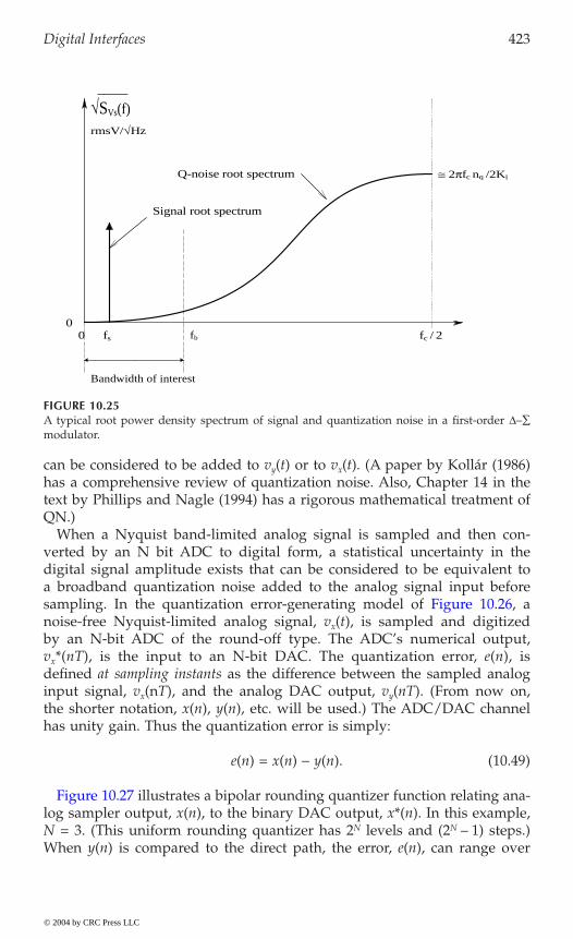
Digital Interfaces 423
can be considered to be added to vy(t) or to vx(t). (A paper by Kollár (1986)has a comprehensive review of quantization noise. Also, Chapter 14 in thetext by Phillips and Nagle (1994) has a rigorous mathematical treatment ofQN.)
When a Nyquist band-limited analog signal is sampled and then con-verted by an N bit ADC to digital form, a statistical uncertainty in thedigital signal amplitude exists that can be considered to be equivalent toa broadband quantization noise added to the analog signal input before
noise-free Nyquist-limited analog signal, vx(t), is sampled and digitizedby an N-bit ADC of the round-off type. The ADC’s numerical output,vx*(nT), is the input to an N-bit DAC. The quantization error, e(n), isdefined at sampling instants as the difference between the sampled analoginput signal, vx(nT), and the analog DAC output, vy(nT). (From now on,the shorter notation, x(n), y(n), etc. will be used.) The ADC/DAC channelhas unity gain. Thus the quantization error is simply:
e(n) = x(n) - y(n). (10.49)
log sampler output, x(n), to the binary DAC output, x*(n). In this example,N = 3. (This uniform rounding quantizer has 2N levels and (2N – 1) steps.)When y(n) is compared to the direct path, the error, e(n), can range over
FIGURE 10.25A typical root power density spectrum of signal and quantization noise in a first-order D–Âmodulator.
fc / 2fs00
rmsV/√Hz
_____
√SVs(f)
≅ 2πfc nq /2KiQ-noise root spectrum
Signal root spectrum
Bandwidth of interest
fb
© 2004 by CRC Press LLC
sampling. In the quantization error-generating model of Figure 10.26, a
Figure 10.27 illustrates a bipolar rounding quantizer function relating ana-

424 Analysis and Application of Analog Electronic Circuits
±q/2 in the center of the range, where q is the voltage step size of theADC/DAC. It is easy to see that for full dynamic range, q should be:
(10.50)
where VxMAX is the maximum (peak-to-peak) value of the input, vx(t), tothe ADC/DAC system.
FIGURE 10.26A quantization noise error-generating model for an ideal N-bit ADC driving an N-bit ideal DAC.
FIGURE 10.27A 3-bit rounding quantizer I/O function.
x(n)N-bit ADC N-bit DAC
x*(n) y(n)
−+
Sampler
x(t)e(n)
Ts
x*(n)
111
110
101
100
011
001−4Vm /7
3Vm /7
qq/2 2q 3q 4q
−q−2q−3q−4qx(n)
010
q = Vm /7
000
Vm
q = (2N − 1)N = 3
(7 steps8 levels)
x*(n) = x(n)
qVxMAX
N=-( )2 1
volts
© 2004 by CRC Press LLC
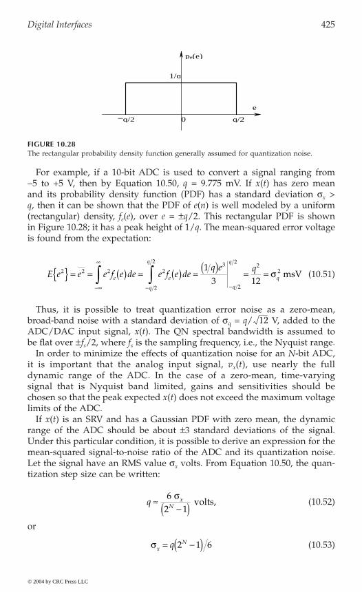
Digital Interfaces 425
For example, if a 10-bit ADC is used to convert a signal ranging from-5 to +5 V, then by Equation 10.50, q = 9.775 mV. If x(t) has zero meanand its probability density function (PDF) has a standard deviation sx >q, then it can be shown that the PDF of e(n) is well modeled by a uniform(rectangular) density, fe(e), over e = ±q/2. This rectangular PDF is shownin Figure 10.28; it has a peak height of 1/q. The mean-squared error voltageis found from the expectation:
(10.51)
Thus, it is possible to treat quantization error noise as a zero-mean,broad-band noise with a standard deviation of sq = q/ V, added to theADC/DAC input signal, x(t). The QN spectral bandwidth is assumed tobe flat over ±fs/2, where fs is the sampling frequency, i.e., the Nyquist range.
In order to minimize the effects of quantization noise for an N-bit ADC,it is important that the analog input signal, vx(t), use nearly the fulldynamic range of the ADC. In the case of a zero-mean, time-varyingsignal that is Nyquist band limited, gains and sensitivities should bechosen so that the peak expected x(t) does not exceed the maximum voltagelimits of the ADC.
If x(t) is an SRV and has a Gaussian PDF with zero mean, the dynamicrange of the ADC should be about ±3 standard deviations of the signal.Under this particular condition, it is possible to derive an expression for themean-squared signal-to-noise ratio of the ADC and its quantization noise.Let the signal have an RMS value sx volts. From Equation 10.50, the quan-tization step size can be written:
(10.52)
or
(10.53)
FIGURE 10.28The rectangular probability density function generally assumed for quantization noise.
e
q/20−q/2
pe(e)
1/q
E e e e f e de e f e deq e q
e e
q
q
q
q
q2 2 2 2
2
2 3
2
22
213 12 = = ( ) = ( ) = ( ) = =
-
- -Ú Ú s msV
12
q xNª
-( )6
2 1s
volts,
sxNq= -( )2 1 6
© 2004 by CRC Press LLC
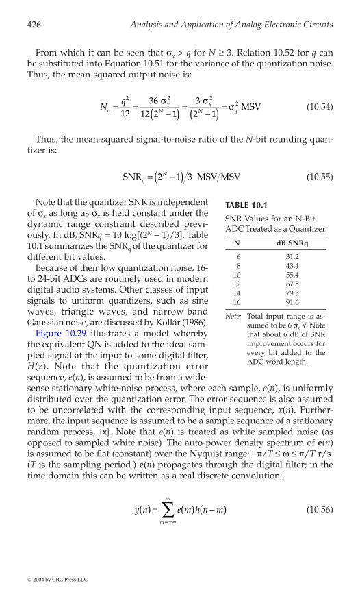
426 Analysis and Application of Analog Electronic Circuits
From which it can be seen that sx > q for N ≥ 3. Relation 10.52 for q canbe substituted into Equation 10.51 for the variance of the quantization noise.Thus, the mean-squared output noise is:
(10.54)
Thus, the mean-squared signal-to-noise ratio of the N-bit rounding quan-tizer is:
(10.55)
Note that the quantizer SNR is independentof sx as long as sx is held constant under thedynamic range constraint described previ-ously. In dB, SNRq = 10 log[(2N - 1)/3]. Table10.1 summarizes the SNRq of the quantizer fordifferent bit values.
Because of their low quantization noise, 16-to 24-bit ADCs are routinely used in moderndigital audio systems. Other classes of inputsignals to uniform quantizers, such as sinewaves, triangle waves, and narrow-bandGaussian noise, are discussed by Kollár (1986).
the equivalent QN is added to the ideal sam-pled signal at the input to some digital filter,H(z). Note that the quantization errorsequence, e(n), is assumed to be from a wide-sense stationary white-noise process, where each sample, e(n), is uniformlydistributed over the quantization error. The error sequence is also assumedto be uncorrelated with the corresponding input sequence, x(n). Further-more, the input sequence is assumed to be a sample sequence of a stationaryrandom process, x. Note that e(n) is treated as white sampled noise (asopposed to sampled white noise). The auto-power density spectrum of e(n)is assumed to be flat (constant) over the Nyquist range: -p/T £ w £ p/T r/s.(T is the sampling period.) e(n) propagates through the digital filter; in thetime domain this can be written as a real discrete convolution:
(10.56)
Nq
ox
Nx
N q= =-( ) =
-( ) =2 2 2
2
1236
12 2 13
2 1s s
s MSV
SNR MSV MSVqN= -( )2 1 3
TABLE 10.1
SNR Values for an N-Bit ADC Treated as a Quantizer
N dB SNRq
6 31.28 43.4
10 55.412 67.514 79.516 91.6
Note: Total input range is as-sumed to be 6 sx V. Notethat about 6 dB of SNRimprovement occurs forevery bit added to theADC word length.
y n e m h n mm
( ) = ( ) -( )= -
Â
© 2004 by CRC Press LLC
Figure 10.29 illustrates a model whereby
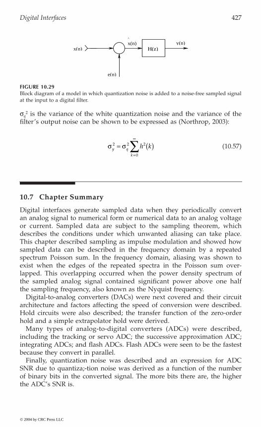
Digital Interfaces 427
sq2 is the variance of the white quantization noise and the variance of the
filter’s output noise can be shown to be expressed as (Northrop, 2003):
(10.57)
10.7 Chapter Summary
Digital interfaces generate sampled data when they periodically convertan analog signal to numerical form or numerical data to an analog voltageor current. Sampled data are subject to the sampling theorem, whichdescribes the conditions under which unwanted aliasing can take place.This chapter described sampling as impulse modulation and showed howsampled data can be described in the frequency domain by a repeatedspectrum Poisson sum. In the frequency domain, aliasing was shown toexist when the edges of the repeated spectra in the Poisson sum over-lapped. This overlapping occurred when the power density spectrum ofthe sampled analog signal contained significant power above one halfthe sampling frequency, also known as the Nyquist frequency.
Digital-to-analog converters (DACs) were next covered and their circuitarchitecture and factors affecting the speed of conversion were described.Hold circuits were also described; the transfer function of the zero-orderhold and a simple extrapolator hold were derived.
Many types of analog-to-digital converters (ADCs) were described,including the tracking or servo ADC; the successive approximation ADC;integrating ADCs; and flash ADCs. Flash ADCs were seen to be the fastestbecause they convert in parallel.
Finally, quantization noise was described and an expression for ADCSNR due to quantiza;-tion noise was derived as a function of the numberof binary bits in the converted signal. The more bits there are, the higherthe ADC’s SNR is.
FIGURE 10.29Block diagram of a model in which quantization noise is added to a noise-free sampled signalat the input to a digital filter.
^
x(n)x(n) H(z)
e(n)
y(n)
s sy qk
h k2 2 2
0
= ( )=
Â
© 2004 by CRC Press LLC

428 Analysis and Application of Analog Electronic Circuits
Home Problems
10.1 A 16-bit ADC is used to convert an audio signal ranging over ±1 V.
a. Find the size of the quantization step, q, required.b. Find the RMS quantization noise associated with full-scale oper-
ation of this ADC.c. Let vin(t) = 1 sin(wo t). Find the RMS SNR at the ADC output in
decibels.
10.2 Consider the 4-bit resistive ladder DAC shown in Figure P10.2.
a. Use superposition to find an expression for Vo = f(Io, I1, I2, I3). LetR = 1 kW and Io = 1 mA dc.
b. What values should I1, I2, and I3 have to make a binary DAC?What is the max. Vo?
10.3problem you will examine the dynamics of this system. A simplified circuit is
characterized by Rin = ; IB = Vos = Rout = 0; and Vo = (-Kvo wb)/(s + wb).
a. Find an algebraic expression for Vo/VR(s).b. Assume VR(s) = VRo/s (step input). Give an expression for Vo(s).
Plot and dimension a general vo(t).c. Let k = 0, N = 8; sketch and dimension vo(t).d. Let k = N - 1 = 7; sketch and dimension vo(t).e. Find a general expression for the maximum slope of vo(t) in terms
of k and other system parameters.f. Let VRo = 1 V and the op amp’s GBWP = Kvo wb = 3 ¥ 108. Find
Vomax° for k = 0 and k = 7. What must the op amp’s slew rate be
to avoid slew-rate limiting of Vo(t)?
FIGURE P10.2
R R
R R
2R 2R
ID
I0I1I2I3
V1R V2V3
IOAVo
© 2004 by CRC Press LLC
Refer to the text Figure 10.5 for the switched weighted capacitor DAC; in this
shown in Figure P10.3. In this circuit, k = 0, 1, 2, …, N - 1. The op amp is

Digital Interfaces 429
10.4 Figure P10.4 illustrates an N = 8-bit MOSFET current-scaling DAC. Thefeedback action of the left-hand op amp forces the Q1 drain current to be ID =VR/(2N R). The left-hand op amp also puts all the connected FET gates atvirtual ground (0). The right-hand op amp forces the FET drains connected toit to be at virtual ground (0). Because all of the MOSFETs are matched andthey all have the same drain, gate, and source voltage, they all have the samedrain current, ID. Write an expression for Vo = f (bk, VR).
10.5Note that the ideal op amp’s summing junction is at virtual ground, so the netcharge flowing into the kth input capacitor when bk = 1 must also equal thecharge accumulated in CF = 2C/K. That is, Qk = VRC/2k = QF = Vo 2C/K. Write
an expression for Vo = f (bk, VR, K); use superposition.
10.6 An 8-bit successive approximation ADC has a reference voltage,VR, set to10.0 V at 25∞C. Find the maximum allowable temperature coefficient of VR inmV/∞C that will allow an error of no more than plus or minus one half LSBover an operating temperature range of 0 to 50∞C.
10.7 A 100-mV peak-to-peak sinusoidal signal is the input to a 12-bit ADC thathas a bipolar offset binary output and a full-scale input range of ±2.5 V.
FIGURE P10.3
FIGURE P10.4
2N C
Vi’
2k C
VR
+
− VoOA
22 matched FETs 21 matched FETs2N −1 matched FETs
21 ID ID22 ID2N −1 ID
ID
R
IOA
IOAVo
b0 bN −3 bN −2 bN −1
1 1110 0 0 0
VGSVGS+
+
2N R
VR
(0)
Q1
© 2004 by CRC Press LLC
Figure P10.5 illustrates an N-bit binary-weighted charge amplifier DAC.
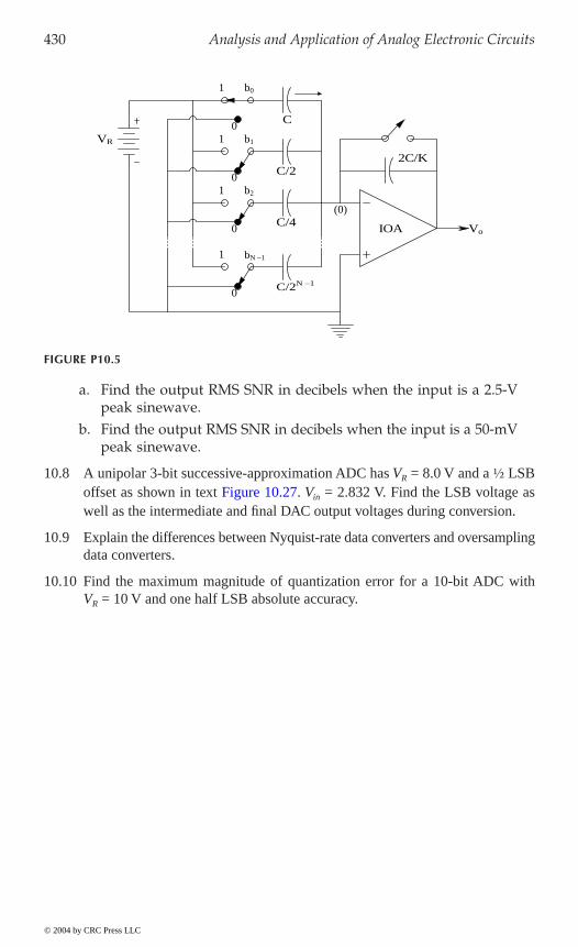
430 Analysis and Application of Analog Electronic Circuits
a. Find the output RMS SNR in decibels when the input is a 2.5-Vpeak sinewave.
b. Find the output RMS SNR in decibels when the input is a 50-mVpeak sinewave.
10.8 A unipolar 3-bit successive-approximation ADC has VR = 8.0 V and a ½ LSB
in
well as the intermediate and final DAC output voltages during conversion.
10.9 Explain the differences between Nyquist-rate data converters and oversamplingdata converters.
10.10 Find the maximum magnitude of quantization error for a 10-bit ADC withVR = 10 V and one half LSB absolute accuracy.
FIGURE P10.5
C/2N −1
C/4
C/2
C
VR
2C/K
b0
b1
b2
bN −1
1
1
1
1
0
0
0
0
(0)
IOA Vo
© 2004 by CRC Press LLC
offset as shown in text Figure 10.27. V = 2.832 V. Find the LSB voltage as

431
11Modulation and Demodulation of Biomedical Signals
11.1 Introduction
In general, modulation is a process by which a dc or low-frequency signalof interest is combined nonlinearly with a high-frequency carrier wave toform a modulated carrier suitable for transmission to a receiver/demodulatorwhere the signal is recovered. Modulators and demodulators form essentialcomponents of most communication and data transmission systems. Somemodulation schemes involve multiplication of the carrier with a function ofthe modulating signal.
In biomedical engineering, recorded physiological signals are modulatedbecause modulation permits robust transmission by wire or coaxial cable,fiber optic cable, or radio (telemetry by electromagnetic waves) from therecording site to the site where the signal will be demodulated, processed,and stored. As an example, in biotelemetry, physiological signals such as theECG and blood pressure modulate a carrier sent as an FM radio signal froman ambulance to a remote receiver (in a hospital ER) where the signals aredemodulated, interpreted, filtered, digitized, and stored. Five major formsof modulation involve altering a high-frequency sinusoidal carrier wave:(1) amplitude modulation (AM); (2) single-sideband AM (SSBAM); (3) fre-quency modulation (FM); (4) phase modulation (PhM); and (5) double-side-band, suppressed-carrier modulation (DSBSCM).
Modulation can also be done using a square wave (or TTL) carrier andcan involve FM, NBFM, and PhM. Delta modulation, pulse-position modu-lation (PPM), and pulse-width modulation (PWM) at constant frequency aredone with digital carrier. AM, FM, and DSBSCM are expressed mathemati-cally below for a sinusoidal carrier. vm(t) is the actual physiological signal.The maximum frequency of vm(t) must be wc, the carrier frequency. Thenormalized modulating signal, m(t), is defined by the following equation:
© 2004 by CRC Press LLC
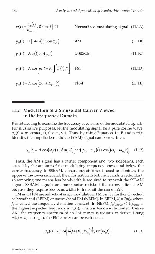
432 Analysis and Application of Analog Electronic Circuits
(11.1A)
(11.1B)
(11.1C)
(11.1D)
(11.1E)
11.2 Modulation of a Sinusoidal Carrier Viewed in the Frequency Domain
It is interesting to examine the frequency spectrums of the modulated signals.For illustrative purposes, let the modulating signal be a pure cosine wave,vm(t) = mo cos(wm t), 0 < mo £ 1. Thus, by using Equation 11.1B and a trig.identity, the amplitude modulated (AM) signal can be rewritten:
(11.2)
Thus, the AM signal has a carrier component and two sidebands, eachspaced by the amount of the modulating frequency above and below thecarrier frequency. In SSBAM, a sharp cut-off filter is used to eliminate theupper or the lower sideband; the information in both sidebands is redundant,so removing one means less bandwidth is required to transmit the SSBAMsignal. SSBAM signals are more noise resistant than conventional AMbecause they require less bandwidth to transmit the same m(t).
FM and PhM are subsets of angle modulation. FM can be further classifiedas broadband (BBFM) or narrowband FM (NBFM). In BBFM, Kf ∫ 2pfd, wherefd is called the frequency deviation constant. In NBFM, fd/fmmax 1 fmmax isthe highest expected frequency in vm(t), which is bandwidth-limited. UnlikeAM, the frequency spectrum of an FM carrier is tedious to derive. Usingm(t) = mo cos(wm t), the FM carrier can be written as:
(11.3)
m tv tv
m tm
m
( ) = ( ) £ ( ) £max
, 0 1 Normalized modulating signal
y t A m t tm c( ) = + ( )[ ] ( )1 cos w AM
y t Am t tm c( ) = ( ) ( )cos w DSBSCM
y t A t K m t dtm c f
t
( ) = + ( )È
ÎÍ
ù
ûúÚcos w FM
y t A t K m tm c p( ) = + ( )[ ]cos w PhM
y t A t Am t tm c o c m c m( ) = ( ) + ( ) +( )( ) + -( )( )[ ]cos cos cosw w w w w2
y t A t K m tm c f m o m( ) = + ( ) ( )ÈÎÍ
ùûú
cos sinw w wa b
© 2004 by CRC Press LLC

Modulation and Demodulation of Biomedical Signals 433
Using the trigonometric identity cos(a + b) = cos(a)cos(b) - sin(a)sin(b),Equation 11.3 can be written as:
(11.4)
Now the cos[(Kf/wm)mo sin(wm t)] and sin[(Kf /wm)mo sin(wm t)] terms canbe expressed as two Fourier series whose coefficients are ordinary Besselfunctions of the first kind and argument b (Clarke and Hess, 1971); note thatb ∫ mo 2pfd/wm:
(11.5A)
(11.5B)
The two Bessel sum relations for cos[b sin(wmt)] and sin[b sin(wm t)] canbe recombined with Equation 11.4 using the trigonometric identities cos(x)cos(y) = ½[cos(x + y) + cos(x - y)] and sin(x) sin(y) = ½[cos(x - y) - cos(x + y)],and one can finally write for the FM carrier spectrum, letting mo = 1:
(11.6)
At first inspection, this result appears quite messy. However, it is evidentthat the numerical values of the Bessel terms tend to zero as n becomes large.For example, let b = 2pfd/wm = 1; then J0(1) = 0.7852; J1(1) = 0.4401; J2(1) =0.1149; J3(1) = 0.01956; J4(1) = 0.002477; J5(1) = 0.0002498; J6(1) = 0.00002094;etc. Bessel constants Jn(1) for n ≥ 4 contribute less than 1% each to the ym(t)spectrum, so they can be neglected. Thus, the practical bandwidth of the FMcarrier, ym(t), for b = 1 is ±3wm around the carrier frequency, wc. In general,as b increases, so does the effective bandwidth of the FM ym(t). For example,
y t A t K m t
A t K m t
m c f m m
c f m m
( ) = ( ) ( ) ( )[ ]- ( ) ( ) ( )[ ]
cos cos sin
sin sin sin
w w w
w w w
0
0
cos sin cosb w b b wm n mn
t J J n t( )[ ] = ( ) + ( ) ( )=
Â0 21
2 2
sin sin sinb w b wm n mn
t J n t( )[ ] = ( ) +( )( )+=
Â2 2 12 10
y t A J t J t t
J t t
J t t
m c c m c m
c m c m
c m c m
( ) = ( ) ( ) + ( ) +( )( ) - -( )( )[ ]+ ( ) +( )( ) + -( )( )[ ]+ ( ) +( )( ) + -( )( )
0 1
2
3
2 2
3 3
b w b w w w w
b w w w w
b w w w w
cos cos cos
cos cos
cos cos[[ ]+ ( ) +( )( ) + -( )( )[ ]+ ( ) +( )( ) + -( )( )[ ] + º
cos cos
cos cos
J t t
J t t
c m c m
c m c m
4
5
4 4
5 5
b w w w w
b w w w w
© 2004 by CRC Press LLC

434 Analysis and Application of Analog Electronic Circuits
when b = 5, the bandwidth becomes ±8wm around wc and when b = 10, thebandwidth required is ±14wm around wc (Clarke and Hess, 1971).
In the case of NBFM, b 1. Thus, the modulated carrier can be written:
(11.7A)
Ø
(11.7B)
With the exception of signs of the sideband terms, the NBFM spectrum isvery similar to the spectrum of an AM carrier (Zeimer and Tranter, 1990); sumand difference frequency sidebands are produced around a central carrier.
The spectrum of a double-sideband suppressed carrier (DSBSCM) signalis given by:
(11.8)
i.e., ideally, the information is contained in the two sidebands; there is nocarrier.
DSBSCM is widely used in instrumentation and measurement systems.For example, it is the natural result when a light beam is chopped in aphotonic instrument such as a spectrophotometer; it also results when aWheatstone bridge is given ac (carrier) excitation and nulled, then one ormore arm resistances are slowly varied in time around its null value (see
variable differential transformer) length sensor as the core is moved in andout (Northrop, 1997). Figure 11.1(B) illustrates a simple system used todemodulate DSBSCM signals.
11.3 Implementation of AM
11.3.1 Introduction
Equation 11.1B indicates that multiplication is inherent in the AM process.In practice, an actual analog multiplier can be used or effective multiplication
y t A t K tm c f m m( ) = + ( ) ( )È
ÎÍÍ
ù
ûúú
cos sinw w wa b
y t A t t t t
A t t t
A t t t
m c m c m
c c m
c c m c m
( ) = ( ) ( )[ ] - ( ) ( )[ ] @ ( ) ( ) - ( ) ( )[ ] = ( ) - ( ) -( )( ) - +( )( )[ ]
cos cos sin sin sin sin
cos sin sin
cos cos cos
w b w w b w
w w b w
w b w w w w
1
2
y t Am t t
Am t t
m o m c
o c m c m
( ) = ( ) ( )= ( ) +( )( ) + -( )( )[ ]
cos cos
cos cos
w w
w w w w2
© 2004 by CRC Press LLC
Figure 11.1(A)). DSBSCM is also present at the output of an LVDT (linear
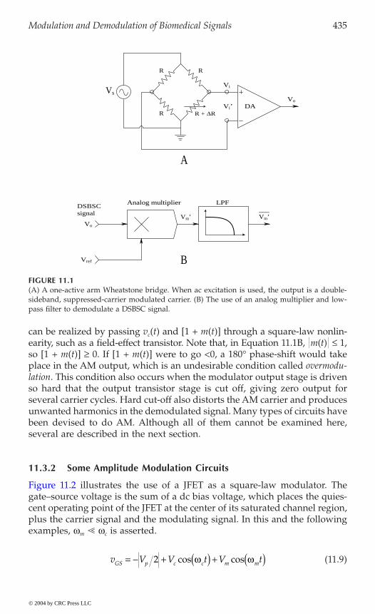
Modulation and Demodulation of Biomedical Signals 435
can be realized by passing vc(t) and [1 + m(t)] through a square-law nonlin-earity, such as a field-effect transistor. Note that, in Equation 11.1B, m(t) £ 1,so [1 + m(t)] ≥ 0. If [1 + m(t)] were to go <0, a 180∞ phase-shift would takeplace in the AM output, which is an undesirable condition called overmodu-lation. This condition also occurs when the modulator output stage is drivenso hard that the output transistor stage is cut off, giving zero output forseveral carrier cycles. Hard cut-off also distorts the AM carrier and producesunwanted harmonics in the demodulated signal. Many types of circuits havebeen devised to do AM. Although all of them cannot be examined here,several are described in the next section.
11.3.2 Some Amplitude Modulation Circuits
gate–source voltage is the sum of a dc bias voltage, which places the quies-cent operating point of the JFET at the center of its saturated channel region,plus the carrier signal and the modulating signal. In this and the followingexamples, wm wc is asserted.
(11.9)
FIGURE 11.1(A) A one-active arm Wheatstone bridge. When ac excitation is used, the output is a double-sideband, suppressed-carrier modulated carrier. (B) The use of an analog multiplier and low-pass filter to demodulate a DSBSC signal.
R + ∆R
RR
R
VsVi
Vi’
___Vm’
LPFAnalog multiplier
Vm’
Vref
Vo
DSBSCsignal
DAVo
A
B
v V V t V tGS p c c m m= - + ( ) + ( )2 cos cosw w
© 2004 by CRC Press LLC
Figure 11.2 illustrates the use of a JFET as a square-law modulator. The
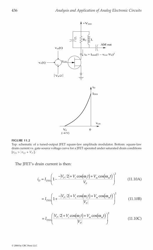
436 Analysis and Application of Analog Electronic Circuits
The JFET’s drain current is then:
(11.10A)
(11.10B)
(11.10C)
FIGURE 11.2Top: schematic of a tuned-output JFET square-law amplitude modulator. Bottom: square-lawdrain current vs. gate-source voltage curve for a JFET operated under saturated drain conditions[vDS > vGS + VP ].
−
+VDD
LRTC
iD = IDSS(1 − vGS /VP)2
AM out
iD
IDSS
vGS
VP
(−4 V)0
vGSvc(t)
vm(t)
VP/2
i IV V t V t
VD DSSP c c m m
P
= -- + ( ) + ( )Ê
ËÁ1
22
cos cosw w
= +- + ( ) + ( )Ê
ËÁI
V V t V t
VDSSP c c m m
P
12
2cos cosw w
=+ ( ) + ( )Ê
ËÁI
V V t V t
VDSSP c c m m
P
22
cos cosw w
© 2004 by CRC Press LLC
Modulation and Demodulation of Biomedical Signals 437
Equation 11.10E shows that the drain current has dc terms, terms at wm
and 2wm, terms at wc and 2wc, and the sideband terms at wc + wm and wc -wm. The dc terms are eliminated by the output coupling capacitor. The RLC“tank” circuit is resonant around wc and so selects the wc and sideband terms.The AM output voltage is approximately:
i.e., the resonant circuit attenuates all frequencies not immediately around wc.
amplifier with a high Q output resonant circuit. The modulating signal, vm(t),is added to a dc gate bias and the RF carrier source. The radio-frequencychokes (RFC) are inductors with very high reactance around wc; they passcurrents from dc to wmmax. The principle of sideband generation is verysimilar to the preceding JFET example. JFETs and MOSFETs have square-law iD vs. vGS curves.
architecture. Q3 and Q4 modulate the collector currents in Q1 and Q1 bychanging the gm of these transistors; for example, gm1 = ICQ1/VT. The operatingpoints of Q1 and Q2 are identical and are affected by IC4 = IE1 + IE2, which isin turn a function of the modulating signal, vm(t). Clarke and Hesse (1971)give a detailed analysis of this transconductance modulator.
Still another approach to AM generation is illustrated in the block diagram
the nonlinearities contain a linear (a1) term as well as the square-law (a2)term. The signals are:
(11.12A)
(11.12B)
= ( ) + ( ) + ( ) +(( ) + ( )[ ] + ( ) ( )[ ]
I V V V t V t
V V t V t V V t t
DSS P P c c m m
P c c m m c m c m
2 2 2 2 2 24
2
cos cos
cos cos cos cos
w w
w w w w
(11.10D)
i I V V V t V t
V V t V t V V t t ta t
D DSS P P c c m m
P c c m m c m c m
= ( ) + + ( )[ ] + ( )[ ] +(( ) + ( )[ ] + ( )( ) + ( )( )[ ]
2 2 2 12
2 2 12
24 1 2 2cos cos
cos cos cos cos
w w
w w w w
(11.10E)
v R I V V V t V V t to T DSS P P c c c m c m c m@ - ( ) ( ) + +( )( ) + -( )( )[ ] 2 cos cos cosw w w w w
(11.11)
w t V t m t mc c( ) = ( ) + + ( )[ ] £cos , .maxw 1 1
z t V t m tc c( ) = ( ) - + ( )[ ]cos ,w 1
© 2004 by CRC Press LLC
Figure 11.3 illustrates the architecture of a class C MOSFET RF power
The BJT circuit of Figure 11.4 illustrates another amplitude modulator
of Figure 11.5. This system is basically a quarter square multiplier, except
438 Analysis and Application of Analog Electronic Circuits
FIGURE 11.3A class C MOSFET tuned RF power amplifier in which the low-frequency modulating signalis added to the carrier voltage at the gate. Miller input capacitance at the gate is cancelled bypositive feedback through the small neutralizing capacitor, CN.
FIGURE 11.4A transconductance-type amplitude modulator using npn BJTs. The circuit effectively multipliesthe carrier by the modulating signal, producing an AM output.
RFC
RFCvc(t)
AM out
Tank
VDD+
CN
CT
D
S
G
VGG
Modulationxfmr vm(t)
vc(t)
RB3
RB1 RB1
RT LC
Q1 Q2
Q3 Q4
−VEE
vm(t)
AM out
+VCC
© 2004 by CRC Press LLC
Modulation and Demodulation of Biomedical Signals 439
(11.12C)
(11.12D)
x = u - v (11.12E)
(11.12F)
The band-pass filter around (wc - wm) to (wc + wm) selects the AM outputand blocks dc and wm. Many other AM circuits exist; some are practical forhigh-power RF output while others assume the AM output will be amplifiedby a linear RF amplifier.
Double-sideband suppressed carrier modulation (DSBSCM) is anotherform of AM in which little or no carrier frequency power occurs in the outputspectrum. Ideally, DSBSCM follows Equation 11.1C, i.e., DSBSCM results asthe product of a low-frequency modulating signal multiplying a high-fre-quency carrier voltage.
Many processes are inherent generators of DSBSCM. For example, see
on DR/R. The bridge is given ac excitation so that its sensitivity will beenhanced. Developing an expression for Vo using voltage-divider relations,
(11.13)
FIGURE 11.5Block diagram of a quarter-square multiplier used for amplitude modulation.
a1w + a2w2
a1z + a2z2z
w
BPF
[1 + m(t)]
−
−
+
+
+
AMoutωc
+x y
1
vc(t)
u t a V t a m t
a V t V m t t m t m t
c c
c c c c
( ) = ( ) + + ( )[ ] +
( ) + + ( )[ ] ( ) + + ( ) + ( )[ ] 1 1
22 2 2
1
2 1 1 2
cos
cos cos
w
w w
v t a V t a m t
a V t V m t t m t m t
c c
c c c c
( ) = ( ) - + ( )[ ] +
( ) - + ( )[ ] ( ) + + ( ) + ( )[ ] 1 1
22 2 2
1
2 1 1 2
cos
cos cos
w
w w
x t a a m mt a V t
a V t t
c c c
c c m c m
( ) = + ( ) + ( ) ( ) +
( ) +( )[ ] + -( )[ ] 2 2 4
4
1 1 2
21
2
cos cos
cos cos
w w
w w w w
V VR RR Ri s= +
+D
D2
© 2004 by CRC Press LLC
Figure 11.1(A) for a Wheatstone bridge initially nulled, whose output depends
440 Analysis and Application of Analog Electronic Circuits
(11.14)
The output is found by subtracting Vi¢ from Vi and multiplying the differ-ence by the DA’s gain, KD.
(11.15)
The quantity in the brackets is the DSBSCM product. DR(t) varies at wm.DSBSCM occurs for light-beam chopping in photonic systems, as well as
for the output of the linear variable differential transformer (LVDT) linear
end, an LVDT is a cylinder with a tube in the center running the length ofthe cylinder. In the center of the tube slides a cylindrical, high-permeabilitymagnetic core that couples magnetic flux from the excitation core to the twosecondary coils, which are wound in opposite directions with the samenumber of turns. When the core is centered (x = 0), equal flux intercepts thewinding of both secondary coils and the output EMF is zero. If the coreposition is up (x = +xm), most of the flux is coupled to the upper secondarycoil and Vo is maximum, having the same phase as Vc. If x = -xm, Vo ismaximum and the phase is 180∞ from Vo with x = +xm. In general, the linearpart of the output can be written as:
(11.16)
where ju° is the time rate of change of the ac flux intercepting the N turns of
the upper secondary coil and K is the slope of the linear Vo vs. x curve.m
the output x(t) is given by:
The BPF centered on wc removes the 2a1Vm cos(wmt) term, leaving theDSBSCM output; thus,
(11.18)
DSBSCM is widely encountered in all phases of instrumentation and mea-surement systems; it is the direct result of multiplying the carrier times themodulating signal.
¢ =V VRRi s 2
V K VR
R RK V R R K V R R t to D s D s D s c=
+ÈÎÍ
ùûú
@ [ ] = ( ) ( ) ( )[ ]DD
D D4 2
4 4 cos w
V N K x t V to u c c= -ÊË
¯ = ( ) ( )∞ ∞j j w1 cos
x t u t v t a v t a v t v t
a V t a V V t t
m c m
m m c m c m c m
( ) = ( ) - ( ) = ( ) + ( ) ( )
= ( ) + +( )( ) + -( )( )[ ]2 4
2 2
1 2
1 2cos cos cosw w w w w
(11.17)
y t a V V t tc m c m c m( ) = +( )( ) + -( )( )[ ]2 2 cos cosw w w w
© 2004 by CRC Press LLC
position sensor. A schematic of an LVDT is shown in Figure 11.6. Seen on
Refer to Figure 11.5. If [1 + m(t)] is replaced by v (t), it is easy to see that

Modulation and Demodulation of Biomedical Signals 441
11.4 Generation of Phase and Frequency Modulation
11.4.1 Introduction
Phase and frequency modulation are subsets of angle modulation, whichhas the general form:
ym(t) = A cos[wct + F(t)] (11.19)
The phase argument of the modulated carrier is [wct + F(t)] radians and thefrequency of the modulated carrier is [wc +
°F] r/s. When F(t) = Kft
Úm(t) dt,FM is obtained; when F(t) = Kp m(t), PhM is the result. Many practical anglemodulation and demodulation circuits have been developed since Edwin H.
FIGURE 11.6Top: cross-sectional schematic of an LVDT. The output is a DSBSC modulated carrier. Bottom:transfer curve of the RMS voltage output of the LVDT vs. core position. A 180∞ phase shift inthe output is signified by Vo(x) < 0.
Vo
Vo
xm
−xmx (mm)
−xm
xm
0
Vc
(rms)
Movingmagneticcore
Secondarycoils
+
−
© 2004 by CRC Press LLC
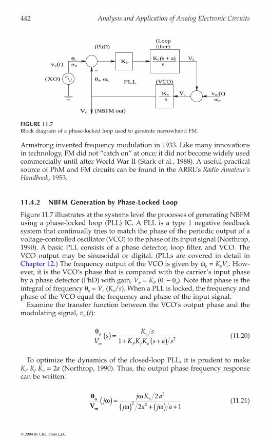
442 Analysis and Application of Analog Electronic Circuits
Armstrong invented frequency modulation in 1933. Like many innovationsin technology, FM did not “catch on” at once; it did not become widely usedcommercially until after World War II (Stark et al., 1988). A useful practicalsource of PhM and FM circuits can be found in the ARRL’s Radio Amateur’sHandbook, 1953.
11.4.2 NBFM Generation by Phase-Locked Loop
Figure 11.7 illustrates at the systems level the processes of generating NBFMusing a phase-locked loop (PLL) IC. A PLL is a type 1 negative feedbacksystem that continually tries to match the phase of the periodic output of avoltage-controlled oscillator (VCO) to the phase of its input signal (Northrop,1990). A basic PLL consists of a phase detector, loop filter, and VCO. TheVCO output may be sinusoidal or digital. (PLLs are covered in detail in
o v c
ever, it is the VCO’s phase that is compared with the carrier’s input phaseby a phase detector (PhD) with gain, Vp = KP (qi - qo). Note that phase is theintegral of frequency qo = Vc (Kv/s). When a PLL is locked, the frequency andphase of the VCO equal the frequency and phase of the input signal.
Examine the transfer function between the VCO’s output phase and themodulating signal, vm(t):
(11.20)
To optimize the dynamics of the closed-loop PLL, it is prudent to makeKP Kf Kv = 2a (Northrop, 1990). Thus, the output phase frequency responsecan be written:
(11.21)
FIGURE 11.7Block diagram of a phase-locked loop used to generate narrowband FM.
ωcvc(t)KP
θi Kf (s + a)s
svm(t)
−
(PhD)(Loopfilter)
(XO) θo, ωc (VCO)
Vo (NBFM out)
ωm
PLL
Kv Vc
VL
qo
m
v
P f vVs
K sK K K s a s
( ) =+ +( )1 2
o
mVj
j K a
j a j avw
ww w
( ) =( ) + ( ) +
2
2 1
2
2 2
© 2004 by CRC Press LLC
Chapter 12.) The frequency output of the VCO is given by w = K V . How-
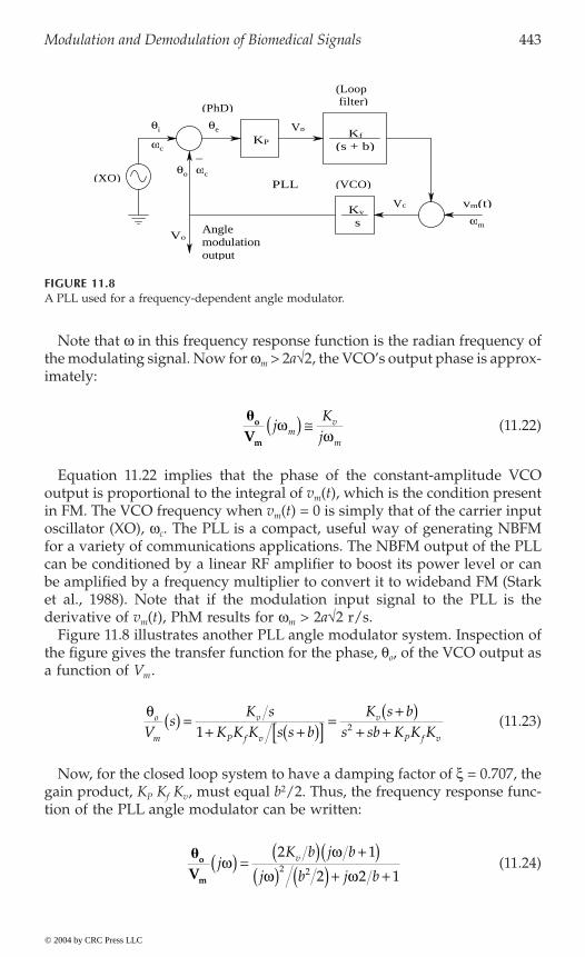
Modulation and Demodulation of Biomedical Signals 443
Note that w in this frequency response function is the radian frequency ofthe modulating signal. Now for wm > 2a÷2, the VCO’s output phase is approx-imately:
(11.22)
Equation 11.22 implies that the phase of the constant-amplitude VCOoutput is proportional to the integral of vm(t), which is the condition presentin FM. The VCO frequency when vm(t) = 0 is simply that of the carrier inputoscillator (XO), wc. The PLL is a compact, useful way of generating NBFMfor a variety of communications applications. The NBFM output of the PLLcan be conditioned by a linear RF amplifier to boost its power level or canbe amplified by a frequency multiplier to convert it to wideband FM (Starket al., 1988). Note that if the modulation input signal to the PLL is thederivative of vm(t), PhM results for wm > 2a÷2 r/s.
Figure 11.8 illustrates another PLL angle modulator system. Inspection ofthe figure gives the transfer function for the phase, qo, of the VCO output asa function of Vm.
(11.23)
Now, for the closed loop system to have a damping factor of x = 0.707, thegain product, KP Kf Kv, must equal b2/2. Thus, the frequency response func-tion of the PLL angle modulator can be written:
(11.24)
FIGURE 11.8A PLL used for a frequency-dependent angle modulator.
(s + b)KfKP
s
(VCO)
(Loopfilter)
(PhD)
(XO)
Vc
Vp
−
Kvvm(t)
θi
θo
θe
ωm
PLL
ωc
ωc
Anglemodulationoutput
Vo
o
mVj
Kjm
v
m
ww( ) @
qo
m
v
P f v
v
P f vVs
K sK K K s s b
K s bs sb K K K
( ) =+ +( )[ ] =
+( )+ +1 2
o
mVj
K b j b
j b j bvw
w
w w( ) = ( ) +( )
( ) ( ) + +
2 1
2 2 12 2
© 2004 by CRC Press LLC
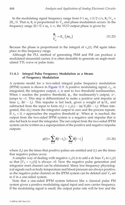
444 Analysis and Application of Analog Electronic Circuits
In the modulating signal frequency range from 0 £ wm £ b/2 r/s, qo/Vm @2Kv/b. That is, qo is proportional to Vm and phase modulation occurs. In thefrequency range 2b/÷2 £ wm £ , the VCO output phase is given by:
(11.25)
Because the phase is proportional to the integral of vm(t), FM again takesplace in this frequency range.
Although the PLL method of generating PhM and FM can produce amodulated sinusoidal carrier, it is often desirable to generate an angle-mod-ulated TTL wave or pulse train.
11.4.3 Integral Pulse Frequency Modulation as a Means of Frequency Modulation
A systems model for a two-sided integral pulse frequency modulationm, is
integrated; the integrator output, v, is sent to two threshold nonlinearities.When v reaches the positive threshold, j+, the nonlinearity’s output, w+,jumps to +1. This step is differentiated to make a positive unit impulse attime tk, d(t - tk). This impulse is fed back, given a weight of j/Ki, andsubtracted from the input to form e(tk) = vm(tk) - (j/Ki)d(t - tk). When inte-grated, this e(tk) resets the integrator output to zero and the process repeats.If vm < 0, v approaches the negative threshold j-. When j- is reached, theoutput from the two-sided IPFM system is a negative unit impulse that isalso fed back to reset the integrator. The net output from the two-sided IPFMsystem can be written as a superposition of the positive and negative impulseoutputs:
(11.26)
where tk are the times that positive pulses are emitted and tj are the timesthat negative pulses occur.
A simpler way of dealing with negative vm(t) is to add a dc bias VB to vm(t)so that [VB + vm(t)] is always >0. Now the negative pulse generation andintegrator reset channel can be eliminated. Many low-frequency physiolog-ical signals such as body temperature and blood pressure are always positive,so the negative pulse channel on the IPFM system can be deleted and VB setto 0 in a one-sided system.
Note that a one-sided IPFM system behaves like a classical pulse FMsystem given a positive modulating signal input and zero carrier frequency.If the modulating signal is small, the output pulse rate will be low and the
o
mv mV
K j= ( )w
y t t t t tkk
jj
( ) = -( ) - -( )=
=
 Âd d1 1
© 2004 by CRC Press LLC
(IPFM) system is shown in Figure 11.9. A positive modulating signal, v
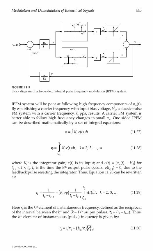
Modulation and Demodulation of Biomedical Signals 445
IPFM system will be poor at following high-frequency components of vm(t).By establishing a carrier frequency with input bias voltage, VB, a classic pulseFM system with a carrier frequency, rc pps, results. A carrier FM system isbetter able to follow high-frequency changes in small vm. One-sided IPFMcan be described mathematically by a set of integral equations:
v = Ú Ki e(t) dt (11.27)
(11.28)
where Ki is the integrator gain; e(t) is its input; and e(t) = [vm(t) + VB] fortk–1 < t < tk. tk is the time the kth output pulse occurs. v(tk-1) = 0, due to thefeedback pulse resetting the integrator. Thus, Equation 11.28 can be rewrittenas:
(11.29)
Here rk is the kth element of instantaneous frequency, defined as the reciprocalof the interval between the kth and (k - 1)th output pulses, tk = (tk - tk-1). Thus,the kth element of instantaneous (pulse) frequency is given by:
(11.30)
FIGURE 11.9Block diagram of a two-sided, integral pulse frequency modulation (IPFM) system.
s
s
s
ϕ−
ϕ+
v
v
w−
v
+1
−1
w+
Ki
ϕ
−
•
w+
Ki
•
w− y
−
y+
y
y
(Reset)
vm(t)
j = ( ) = º -
Ú K e t dt ki
t
t
k
k
, , , ,
1
2 3
rt t
Kt t
e t dt kkk k
ik k t
t
k
k
=-
= ( ) -( ) = º
- --
Ú1 12 3
1 11
j , , ,
r K ek k i k∫ = ( ) 1 t j t
© 2004 by CRC Press LLC
446 Analysis and Application of Analog Electronic Circuits
If vm is zero and the input to the IPFM system is a constant VB ≥ 0, rc =(Ki/j) VB pps. That is, the IPFM output carrier center frequency, rc, is pro-portional to the bias, VB.
As an example of finding the pulse emission times for a one-sided IPFMsystem, consider the input, vm(t) = (4 e-7t) U(t), the threshold j = 0.025 V,Ki = 1, and VB = 0. The first pulse is emitted at t1, which is found from thedefinite integral:
(11.31)
(11.32)
The time the first pulse is emitted, t1, is found to be at 6.391 ¥ 10-3 sec. Thegeneral pulse emission time, tk, is found by recursion. For example, once t1
is known, t2 is found by solving:
(11.33)
In this simple case t2 = 13.081 E-3 sec. Induction is used to find a generalformula for tk:
(11.34)
From Equation 11.34, it can be seen that tk is only defined for a positive ln[*]argument, i.e., for
(11.35)
Thus, kmax = 22; only 22 pulses are emitted.Demodulation of IPFM positive pulse trains can be done by passing the
pulses through a low-pass filter or by actually calculating the pulse train’sinstantaneous frequency by taking the reciprocal of the time interval betweenany two pulses and holding that value until the next pulse [(k + 1)th] occursin the sequence, then repeating the operation. Stated mathematically, instan-taneous pulse frequency demodulation (IPFD) can be written:
j = ( ) Æ =( ) -( )
-( ) Æ -( ) = -( ) ÆÚ Ú-
-v t dte dt
em
t tt
t
0
7
0
71 1
10 0254 7
70 025 7
41.
.
e tt- ( ) -= - ¥ = æ Æææ - = - ¥71
21 17 0 025
40 95625 7 4 47359 10
.. .ln *
j = ( )Ú v t dtm
t
t
1
2
tk
k = -( ) - ¥ ¥ÈÎÍ
ùûú
1 7 17 0 025
4ln
.
k £¥
=47 0 025
22 875.
.
© 2004 by CRC Press LLC

Modulation and Demodulation of Biomedical Signals 447
(11.36)
where
(11.37)
Note that two pulses (k = 2) are required to define the first pulse interval.vm(t)ˆ is a series of steps and the height of each is the (previous) rk. Note
that the IPFD is not limited to the demodulation of IPFM; it has been exper-imentally applied as a descriptor to actual neural spike signals (Northrop,2001).
11.5 Demodulation of Modulated Sinusoidal Carriers
11.5.1 Introduction
Of equal importance in the discussion of modulation is the process of demod-ulation or detection, in which the modulating signal, vm(t), is recovered fromthe modulated carrier, ym(t). Generally, several circuit architectures can beused to modulate a given type of modulated signal and several ways canbe used to demodulate it. In the case of AM (or single-sideband AM), thesignal recovery process is called detection.
11.5.2 Detection of AM
There are several practical means of AM detection (Clarke and Hess, 1971,Chapter 10). One simple form is to rectify and low-pass filter ym(t). Becauserectification is difficult at high radio frequencies, heterodyning or mixing theincoming high-frequency AM signal with a local oscillator (in the receiver)whose frequency is separated by a fixed interval, Df, from that of the incom-ing signal produces mixing frequencies of (fc - flo) = Df. Df is called theintermediate frequency of the receiver and is typically 50 to 455 kHz, or 10.7MHz in commercial FM receivers. High-frequency selectivity IF transformersare used that have tuned primary and secondary windings. Very high IFfrequency selectivity can be obtained with piezoelectric crystal filters orsurface acoustic wave (SAW) tuned IF filters.
Another form of AM detection passes ym(t) through a square-law nonlin-earity followed by a low-pass filter; however, the square-law detector suffers
v t U t t U t tm k k kk
( ) = -( ) = -( ) +=
 t 12
t tk kk kt t
k∫ =-
= º-
11
2 31
, , ,
© 2004 by CRC Press LLC

448 Analysis and Application of Analog Electronic Circuits
from the disadvantage that it generates a second harmonic component ofthe recovered modulating signal. A third way to demodulate an AM carrierof the form given by Equation 11.1B is to mix (multiply) it by a sinusoidalsignal of the same frequency and phase as the carrier component of the ym(t).A phase-locked loop system architecture can be used for this purpose; seeFigure 11.10 (Northrop, 1990). This PLL system uses three multiplicativemixers. The AM input after RF amplification is:
(11.38)
Mixer M1 effectively multiplies x1 ¥ xo. xo is the output of the PLL’s VCO.Thus,
The IF band-pass filter selects the second term, which has frequency closeto wif when the PLL is near lock. This means that x4 is:
(11.40)
Also, the output of the crystal-controlled oscillator (XO) is:
x5 = X5 cos(wif t) (11.41)
FIGURE 11.10Block diagram of a PLL system used to demodulate AM audio signals. Note that three mixers(multipliers) are used; M1 is the quadrature phase detector of the PLL.
RF AM signal
M2
Phaseshift
M3
+90o
Audio BPF
IF BPF
LPF
s
XOIF
ωif
ωif
ω
ω
ωKv
x7 x6
ω4
x4
x5’1 x8
Antennax5
x9Audioout
M1KI
ωo, θo
xo
ωc, θc
xix1
TunedRF amplifier
x A m t tc c1 1= + ( )[ ] +( )sin w q
x A m t t X t
AX m t t t
i c c o o o
o c o c o c o c o
= + ( )[ ] +( ) ¥ +( )= + ( )[ ][ ] +( ) + +[ ] + -( ) + -[ ]
1
1 2
sin cos
sin sin
w q w q
w w q q w w q q
(11.39)
x K AX m t ti o c o c o4 1 2= + ( )[ ][ ] -( ) + -[ ]sin w w q q
© 2004 by CRC Press LLC
Modulation and Demodulation of Biomedical Signals 449
Mathematically, the product, x6 = x4 ¥ x5 is formed:
(11.42A)
(11.42B)
At lock, (wc - wo) = wif r/s and (qc - qo) Æ 0. The low-pass filter acts on x6;its output is the zero-frequency component of x6. Thus:
(11.43)
Note that x7 Æ 0 at lock. Now, x5¢ = X5 sin(wif t), so x8 can be written:
(11.44A)
(11.44B)
Again, at lock:
(11.44C)
The band-pass filter cuts the dc term in x8 and also the 2wif term; therefore,the output of the BPF is proportional to the modulating signal:
(11.45)
Thus, the normalized modulating signal, [mo cos(wm t)], is recovered, timesa scaling constant.
A fourth kind of AM demodulation can be accomplished by finding themagnitude of the modulated signal’s analytical signal (Northrop, 2003).
x K AX m t t X ti o c o c o if6 51 2= + ( )[ ][ ] -( ) + -[ ] ¥ ( )sin cosw w q q w
x X K AX m t wi o c o if c o
c o if c o
6 5 1 4= + ( )[ ][ ] - +( ) + -[ ]+ - -( ) + -[ ]
sin
sin
w w q q
w w w q q
X X K AX m ti o c o if c o7 5 1 4= + ( )[ ][ ] - -( ) + -[ ]sin w w w q q
x x x K A X m t t
X t
i o c o c o
if
8 4 5
5
1 2= ¥ ¢ = + ( )[ ][ ] -( ) + -[ ] ¥
( )sin
sin
w w q q
w
x X K A X m t
t t
i o
c o if c o c o if c o
8 5 1 4= + ( )[ ][ ]- -( ) + -[ ] - - +( ) + -[ ] cos cosq q w q q q q w q q
x X K A X m t t ci o if o8 5 1 4 0 2= + ( )[ ][ ] ( ) - ( ) + -[ ] cos cos w q q
x X K AX m ti o9 5 4= ( )
© 2004 by CRC Press LLC

450 Analysis and Application of Analog Electronic Circuits
Examine the widely used rectifier + low-pass filter (average envelope) AMdetector. Figure 11.11(A) illustrates a low-frequency modulating signal, m(t).Figure 11.11(B) shows the amplitude-modulated carrier (the sinusoidal car-rier is drawn with straight lines for simplicity). Figure 11.11(C) illustratesthe block diagram of a simple half-wave rectifier circuit followed by a band-pass filter to exclude dc and terms of carrier frequency and higher. The half-wave rectification process can be thought of as multiplying the AM ym(t) bya 0,1 switching function, Sq(t), in phase with the carrier. Mathematically, thiscan be stated as:
(11.46)
FIGURE 11.11AM detection by simple half-wave rectification. (A) The modulating signal. (B) The AM carrier(drawn as a triangle wave instead of a sinusoid). (C) An ideal half-wave rectifier followed byan audio band-pass filter.
ym(t)
m(t)
ymdf(t)
BPFHWR
ym(t)+
ymr(t)
ymr
ym
f
A
B
C
y t A m t t Sq t
A t Sq t A m t t Sq t
mr m c
c o m c
( ) = + ( )[ ] ( ) ( )
= ( ) ( ) + ( ) ( ) ( )
1 cos cos
cos cos cos
w w
w w w
© 2004 by CRC Press LLC
Modulation and Demodulation of Biomedical Signals 451
Sq(t) can be written as a Fourier series (Northrop, 2003):
(11.47A)
Ø
(11.47B)
Now multiply the Fourier series by the terms of Equation 11.46:
and examine what happens when the terms of Equation 11.48 are passedthrough a band-pass filter that attenuates to zero dc and all terms at above(wc - wm). Trigonometric expansions of the form cos(x) cos(y) = (1/2)[cos(x + y) + cos(x - y)] are used. Let the BPF’s output be ymdf (t):
(11.49)
The BPF output contains a dc term plus a term proportional to the desiredmo cos(wmt). Because AM radio is usually used to transmit audio signals thatdo not extend to zero frequency, the band-pass filter blocks the dc but passesmodulating signal frequencies. Thus, ymdf (t) µ mo cos(wmt). Several other AMdetection schemes exist, including peak envelope detection and synchronousdetection, described later in the detection of DSBSCM signals; the interestedreader can find a good description of these modes of AM detection in Clarkeand Hess (1971).
11.5.3 Detection of FM Signals
When modulating and transmitting signals with a dc component, FM is thedesired modulation scheme because a dc signal, Vm, produces a fixed fre-quency deviation from the carrier at wc given by:
Sq tn t
nn
n
c( ) = + ( ) -( ) -( )[ ]-( )
+
=
Â12
1
1
2 12 12 1
pwcos
Sq t t t tc c c( ) = + ( ) ( ) - ( ) ( ) + ( ) ( ) - º 12 2 1 3 3 1 5 5p w w wcos cos cos
y t A t A t t t
t t Am t t
Am t t Am
d c c c c
c c o m c
o m c o
( ) = ( ) + ( ) - ( ) ( ) ( ) +(+ ( ) ( ) ( ) - º + ( ) ( )+ ( ) ( ) ( ) -
12
2
12
2
2 1 3 3
1 5 5
2 2 3
cos cos cos cos
cos cos cos cos
cos cos
w p w w w
w w w w
p w w p(( ) ( ) ( ) ( )+ ( ) ( ) ( ) ( )- ( ) ( ) ( ) ( ) + º
cos cos cos
cos cos cos
cos cos cos
w w w
p w w w
p w w w
m c c
o m c c
o m c c
t t t
Am t t t
Am t t t
3
2 5 5
2 7 7 (11.48)
y t A A m tmdf o m( ) = ( ) + ( ) ( )[ ]p p wcos
© 2004 by CRC Press LLC
452 Analysis and Application of Analog Electronic Circuits
Dw = Kf Vm (11.50)
As in the case of AM, FM demodulation can accomplished by severalmeans. The first step in any FM demodulation scheme is to limit the receivedsignal. Mathematically, limiting can be represented as passing the sinusoidalFM ym(t) through a signum function (symmetrical clipper); the clipper outputis a square wave of peak height, ymcl(t) = B sgn[ym(t)]. (The sgn(ym) functionis 1 for ym ≥ 0, and -1 for ym < 0.) Clipping removes most unwanted amplitudemodulation, including noise on the received ym(t); this is one reason whyFM radio is free of noise compared to AM. The frequency argument of ymcl(t)is the same as for the FM sinusoidal carrier, i.e., wFM = wc + Kf vm(t).
Once limited, several means of FM demodulation are now available,including the phase-shift discriminator; the Foster–Seely discriminator; theratio detector; pulse averaging; and certain phase-locked loop circuits (Chirlian,1981; Northrop, 1990). It is beyond the scope of this text to describe all ofthese FM demodulation circuits in detail, so the simple pulse averagingdiscriminator will first be examined.
In this FM demodulation means, the limited signal is fed into a one-shotmultivibrator that triggers on the rising edge of each cycle of ymcl(t), produc-ing a train of standard TTL pulses, each of fixed width d = p/wc sec. Forsimplicity, assume the peak height of each pulse is 5 V and low is 0 V. Nowthe average pulse voltage is vav(t):
(11.51)
Thus, recovery of vm(t), even a dc vm, requires the linear operation:
(11.52)
In practice, the averaging is done by a low-pass filter with break frequencywmmax wf wc.
In phase modulation, the modulated carrier is given by:
(11.53)
Because the frequency of the PhM carrier is the derivative of its phase,
(11.54)
PhM carriers can be generated and demodulated using phase-locked loops(Northrop, 1989).
v tT
dtK v
dt K vavc f m
f m c
c
( ) = =+
= ( ) +( )Ú Ú15 5 5 2 1
0 0
d p ww
pw
v t v t Km av c f( ) = ( ) ( ) -[ ]( )2 5 1 w
y t A t K v tm c p m( ) = + ( )[ ]cos w
w wPhM c p mK v t= + ( )∞
© 2004 by CRC Press LLC

Modulation and Demodulation of Biomedical Signals 453
Figure 11.12 illustrates an example of a PLL used to recover the modulatingsignal, vm(t), in an NBFM carrier. Note that the PLL input is the phase of theNBFM signal, qi, which is proportional to the integral of vm(t). The PLL triesto track qi(t) and in doing so generates the VCO control signal, vc(t), that isof interest. The frequency in the transfer function of the PLL is the frequencyof vm(t), not wc. The loop gain of the PLL is:
(11.55)
To give the closed-loop PLL a damping of x = 0.707, it is easy to show,using root locus, that KP Kf Kv = b2/2 and the undamped natural frequencyof the PLL is wn = b÷2/2 r/s. The frequency response function for the PLLdemodulator can be shown to be:
(11.56)
Thus, at signal frequencies below the loop’s wn = b÷2/2 r/s, the PLLdemodulates the NBFM input; the output is proportional to vm(t). That is:
(11.57)
Therefore, the loop filter output is proportional to vm(t) for vm frequenciesbetween zero and about wn/2.
11.5.4 Demodulation of DSBSCM Signals
The demodulation of DSBSCM carriers is generally done by a phase-sensitiverectifier (PSR) (also known as a synchronous rectifier) followed by a low-
FIGURE 11.12A PLL used to demodulate an NBFM carrier.
s (s + a)
(Loop filter)(PhD)
(FM process)
Kv
s
(VCO)θo
−
KfKP
vcvpKmvm(t) θi
A sK K K
s s bLP f v( ) = -
+( )
VV
c
m
jK j K K j b
K K K j j bK K
j b j bm p f
P f v
m vww w
w w w w( ) =
( ) +( )+ +( )[ ] =
( ) ( ) + ( ) +1 2 2 12 2
v t K K v tc m v m( ) @ ( ) ( )
© 2004 by CRC Press LLC
pass filter. One version of this system is shown in Figure 11.13. In this op amp

454 Analysis and Application of Analog Electronic Circuits
version of a PSR, an analog MOS switch is made to close for the positivehalf-cycles of the reference signal that has the same frequency and phase as
signal, vm(t), from there, the DSBSCM signal, and, finally, Vz(t), the unfilteredoutput of the PSR. Note that “c” means the MOS switch is closed and “o”means it is open. The simple op amp low-pass filter also inverts, so its output
is proportional to -vm(t).Another means of demodulating a DSBSC signal is by an analog multiplier
followed by an LPF. In the latter means, the multiplier output voltage, Vo¢(t),is the product of a reference carrier and the DSBSCM signal:
(11.58)
The 0.1 constant is inherent to all analog multipliers. By trigonometricidentity, noting that cosq is an even function, the multiplier output can bewritten:
(11.59)
After unity-gain low-pass filtering,
(11.60)
which is certainly proportional to vm(t).Still another way to demodulate DSBSC signals is by a special PLL archi-
successful operation requires that the modulating signal, vm(t), be nonzero
FIGURE 11.13Schematic of a three-op amp synchronous (phase-sensitive) rectifier used to demodulate aDSBSC-modulated carrier.
R R R
R
LPF
OA2 OA3R/2
R
R
SYNCvr(t)
OA1DSBSCsignal −ym(t) MOS switch vz(t)
___vz(t)
C
Vo’
Vz
¢( ) = ( ) ( ) ¥ ( ) +( )( ) + -( )( )[ ]V t B t Am t to c o c m c m0 1 2. cos cos cosw w w w w
¢( ) = ( ) ( ) +( )( ) + ( )[ ]V t Am B t to o c m m0 1 4 2. cos cosw w w
¢( ) = ( ) ( ) ( )V t AB m to o m0 1 4. cos w
© 2004 by CRC Press LLC
the unmodulated carrier. Figure 11.14 illustrates a low-frequency modulating
tecture called the Costas loop (Northrop, 1990), shown in Figure 11.15. Its

Modulation and Demodulation of Biomedical Signals 455
only for short intervals so that the PLL does not lose lock. The input DSBSCMsignal can be written:
x1 = vm(t) Vc cos(wct + qc) (11.61)
The output of the PLL’s VCO is:
x6 = X6 cos(wot + qo) (11.62)
FIGURE 11.14
lating signal. Middle: DSBSC signal. Bottom: Detected signal before LPF.
vm(t)
t
DSBSCM signal
PSD signal(before LPF)Vz
c cc c co o o o o
Switch status
0
0
0
© 2004 by CRC Press LLC
Waveforms relevant to the operation of the synchronous rectifier of Figure 11.13. Top: Modu-
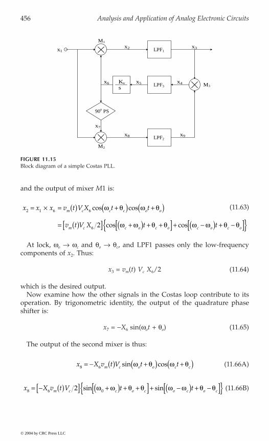
456 Analysis and Application of Analog Electronic Circuits
and the output of mixer M1 is:
At lock, wo Æ wc and qo Æ qc, and LPF1 passes only the low-frequencycomponents of x2. Thus:
x3 = vm(t) Vc X6/2 (11.64)
which is the desired output. Now examine how the other signals in the Costas loop contribute to its
operation. By trigonometric identity, the output of the quadrature phaseshifter is:
x7 = -X6 sin(wot + qo) (11.65)
The output of the second mixer is thus:
(11.66A)
(11.66B)
FIGURE 11.15Block diagram of a simple Costas PLL.
x1x2 x3
s
x7
x8 x9
M2
M1
x4x5x6 Kv M3
90o PS
LPF1
LPF3
LPF2
x x x v t V X t t
v t V X t t
m c c c o o
m c c o c o c o c o
2 1 6 6
6 2
= ¥ = ( ) +( ) +( )= ( )[ ] +( ) + +[ ] + -( ) + -[ ]
cos cos
cos cos
w q w q
w w q q w w q q
(11.63)
x X v t V t tm c o o c c8 6= - ( ) +( ) +( )sin cosw q w q
x X v t V t tm c c o c o c o c8 6 02= - ( )[ ] +( ) + +[ ] + -( ) + -[ ] sin sinw w q q w w q q
© 2004 by CRC Press LLC
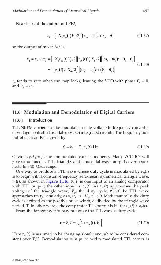
Modulation and Demodulation of Biomedical Signals 457
Near lock, at the output of LPF2,
(11.67)
so the output of mixer M3 is:
(11.68)
x4 tends to zero when the loop locks, leaving the VCO with phase qo = qc
and wo = wc.
11.6 Modulation and Demodulation of Digital Carriers
11.6.1 Introduction
TTL NBFM carriers can be modulated using voltage-to-frequency converteror voltage-controlled oscillator (VCO) integrated circuits. The frequency out-put of such an IC is given by:
fo = k1 + Kv vm(t) Hz (11.69)
Obviously, k1 = fc, the unmodulated carrier frequency. Many VCO ICs willgive simultaneous TTL, triangle, and sinusoidal wave outputs over a sub-hertz to +10-MHz range.
One way to produce a TTL wave whose duty cycle is modulated by vm(t)is to begin with a constant-frequency, zero-mean, symmetrical triangle wave,
T T
with TTL output; the other input is vm(t). As vm(t) approaches the peakvoltage of the triangle wave, Vp, the duty cycle, h, of the TTL waveapproaches unity; similarly, as vm(t) Æ -Vp, h Æ 0. Mathematically, the dutycycle is defined as the positive pulse width, d, divided by the triangle waveperiod, T. In other words, the comparator TTL output is HI for vm(t) > vT(t).
From the foregoing, it is easy to derive the TTL wave’s duty cycle:
(11.70)
Here vm(t) is assumed to be changing slowly enough to be considered con-stant over T/2. Demodulation of a pulse width-modulated TTL carrier is
x X v t V tm c o c o c9 6 2@ - ( )[ ] -( ) + -[ ]w w q q
x x x X v t V v t V X t
v t V X t
m c m c o c o c
m c o c o c
4 9 3 6 6
6
2
2 2
2
= ¥ = - ( )[ ] ( )[ ] -( ) + -[ ]= - ( )[ ] -( ) + -( )[ ]
w w q q
w w q q
h d= = + ( )[ ]T v t Vm p1
2 1
© 2004 by CRC Press LLC
v (t), as shown in Figure 11.16. v (t) is one input to an analog comparator
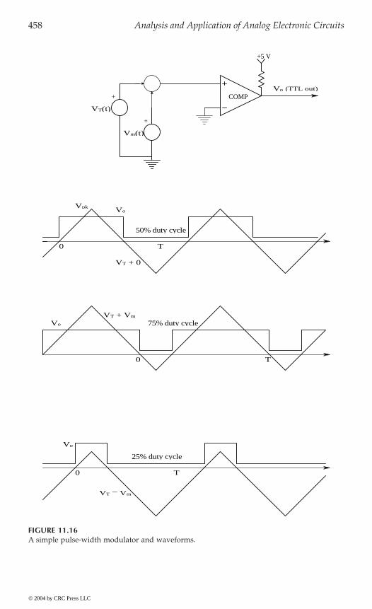
458 Analysis and Application of Analog Electronic Circuits
FIGURE 11.16A simple pulse-width modulator and waveforms.
Vo (TTL out)
+5 V
COMP+
+
VT + 0
VT + Vm
Vo
Vo
VT − Vm
0 T
75% duty cycle
25% duty cycle
0 T
VoVpk
50% duty cycle
T0
VT(t)
Vm(t)
© 2004 by CRC Press LLC
Modulation and Demodulation of Biomedical Signals 459
done by averaging the TTL pulse train and subtracting the dc componentpresent when vm = 0.
11.6.2 Delta Modulation
Now consider delta modulation (DM) and demodulation. A delta modulatoris also known as a 1-bit differential pulse code modulator (DPCM). Theoutput of a delta modulator is a clocked (periodic) train of TTL pulses withamplitudes that are HI or LO, depending on the state of the comparator
of the input signal. The comparator output is TTL HI if e(t) = [vm(t) - vr¢(t)] >0 and LO if e < 0. The D flip-flop’s (DFF) complimentary output (Q = Vo) isLO if the comparator output is HI at a positive transition of the TTL clocksignal. The LO output of the DFF remains LO until the next positive transi-tion of the clock signal; then, if the comparator output has gone LO, Vo goeshigh for one clock period (Tc), etc. vr¢(t) is the output of the analog integratoroffset by Vbias, which is one half the maximum vr ramp height over one clockperiod. Vbias can be shown to be 1.1Tc/(RC) volts.
With this Vbias, when vm(t) = 0, vr¢(t) will oscillate around zero with a trianglewave with zero mean and peak height 1.1Tc/(RC) volts. Note that the Qoutput of the DFF must be used because the integrator gain is negative (i.e.,-1/RC): a HI Vo will cause vr¢ to go negative and a low Vo will make vr¢ gopositive. Note that vr¢(t) is slew rate limited at ±(2.2 V/RC) volts/secondand, if the slope of vm(t) exceeds this value, a large error will accumulate inthe demodulation operation of the DM signal. (Slew rate is simply themagnitude of the first derivative of a signal, i.e., its slope.) When a DMsystem is tracking vm = 0, vr¢(t) oscillates around zero and the DM output isa periodic square-wave 1-bit “noise.”
In adaptive delta modulation (ADM), the magnitude of the error is usedto adjust the effective gain of the integrator to increase the slew rate of vr¢(t)to track rapidly changing vm(t) better. One version of an ADM system is
the signum operation; therefore, the dc value (mean) of the TTL wave mustbe subtracted before it is filtered, absval’d, and used to modulate the size ofthe square wave input to the integrator. A conventional analog multiplier isused as a modulator.
If a large error occurs as a result of poor tracking due to low slew rate invr¢(t), the comparator output will remain HI (or LO) for several clock cycles.This condition produces a nonzero signal at vf , which in turn increases theamplitude of the symmetrical pulse input to the integrator. When the ADMis tracking well, so that vr¢(t) oscillates around a nearly constant vm level,then vf Æ 0 and the peak amplitude of the error remains small. In summary,the ADM acts to minimize the mean squared error between vm(t) and vr¢(t).
There are other variations on DM (e.g., sigma–delta modulation) and othertypes of nonlinear adaptive DM designs in addition to the one shown here.
© 2004 by CRC Press LLC
output shown in Figure 11.17. The DM output basically tracks the derivative
shown in Figure 11.18. Note that, ideally, the comparator should perform
460 Analysis and Application of Analog Electronic Circuits
Much of the interest in efficient, simple, low-noise modulation schemes hasbeen driven by the need to transmit sound and pictures over the Internet.Medical signals such as ECG and EEG also benefit from this developmentbecause of the need to transmit them from the site of the patient to a diag-nostician. Biotelemetry is an important technology in the wireless monitoringof internal physiological states, sports medicine, and emergency medicine,and in ecological studies.
FIGURE 11.17Block diagram and waveforms of a simple delta modulator.
CLOCK
vr’
+ 5 V
vmQ
CP
_Q
COMP. D(TTL)
vc
(TTL)DFF
Vo
C
OA
(Int.)
−2.4 V
Rvr
−Vbias
vm
vr’e
00
_(DFF Q output)
vo
CLOCK
A
B
© 2004 by CRC Press LLC
Modulation and Demodulation of Biomedical Signals 461
11.7 Chapter Summary
Broadly speaking, modulation is a process in which a low-frequency mod-ulating signal acts on a high-frequency carrier wave in some way so that thehigh-frequency modulated carrier can be transmitted (e.g., as radio waves,ultrasound waves, light waves, etc.) to a suitable receiver; after this theprocess of demodulation occurs, recovering the modulating signal. In the
FIGURE 11.18(A) Circuit for an adaptive delta modulator. (B) Demodulator for ADM. A long time-constantLPF is generally used instead of an ideal integrator for filtering vm.
CLOCK
_Q
(TTL)DFFvr’
COMP. D(TTL)
vmQ
CP
vc
+ 5 V
−2.4 V
+1 V
Vo
R
C
(Int.)
OA(AM)
(LPF)
(LPF) (Absval.)
(AM)R
C
vm^
+1 V
vf
vf
−2.4 V
B
A
vr−2.4 V
(Absval.)
−Vbias
Vo
(TTL)
© 2004 by CRC Press LLC
462 Analysis and Application of Analog Electronic Circuits
frequency domain, the low-frequency power spectrum of the signal is trans-lated upward in frequency to lie around the carrier frequency. A majorpurpose of modulation is to permit long-range transmission of the modu-lating signal by a relatively noise-free modality.
Why transmit modulated carriers? After all, traditional short-distance tele-phony transmits audio information directly on telephone lines. The answerlies in the signal spectrum. The low frequencies associated with many endog-enous physiological signals cannot be transmitted by conventional voicetelephony; modulation must be used. The carrier modality can be radiowaves, ultrasound, or light on fiber optic cables. For example, when themodulating signal is an ECG, its power spectrum is too low for directtransmission by telephone lines. However, the ECG can narrow-band fre-quency-modulate (NBFM) an audio-frequency carrier that can be transmittedon phone lines and demodulated at the receiver. In a case in which anambulance is en route carrying a patient, the ECG can directly NBFM an RFcarrier, which is received and demodulated at the hospital’s ER.
Subcarrier modulation can be used as well. Here several low-frequencyphysiological signals such as ECG, blood pressure, and respiration canNBFM an audio subcarrier, each with a different frequency. The modulatedsubcarriers are added together and used to modulate amplitude of frequencyof an RF carrier, which is transmitted. Subcarrier FM can also be used withultrasonic “tags” to monitor marine animals such as whales and dolphins.The tag is attached to the animal and reports such parameters as depth,water temperature, heart rate, etc. The subcarriers are separated followingdetection at the receiver by band-pass filters and then demodulated.
The section about AM examined the process in the frequency domain andgave examples of selected circuits used in AM and single-sideband AM.Double-sideband, suppressed-carrier AM was shown to be the simple resultof multiplying the carrier by the modulating signal. Examples of DSBSCMwere shown to include Wheatstone bridge outputs given ac carrier excitationand the output of an LVDT. Broadband and narrowband FM were examinedtheoretically; circuits and systems used to generate NBFM, such as the phase-locked loop (PLL), were described as well. Integral- and relaxation-pulsefrequency modulation were introduced.
The section on demodulation illustrated circuits and systems used todemodulate AM, DSBSCM, FM, and NBFM signals. Again, the PLL wasshown to be effective at demodulation. Modulation of digital (e.g., TTL, ECL)carriers includes FM and –D (sigma–delta) modulation, pulse-width orduty-cycle modulation, and adaptive delta modulation. Means of demodu-lating digital modulated signals were described.
Home Problems
11.1 An analog pulse instantaneous pulse frequency demodulator (IPFD) mustgenerate a hyperbolic (not exponential) capacitor discharge waveform inorder to convert interpulse intervals to elements of instantaneous frequency
© 2004 by CRC Press LLC
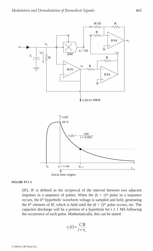
Modulation and Demodulation of Biomedical Signals 463
(IF). IF is defined as the reciprocal of the interval between two adjacentimpulses in a sequence of pulses. When the (k + 1)th pulse in a sequenceoccurs, the kth hyperbolic waveform voltage is sampled and held, generatingthe kth element of IF, which is held until the (k + 2)th pulse occurs, etc. Thecapacitor discharge will be a portion of a hyperbola for t ≥ 1 MS followingthe occurrence of each pulse. Mathematically, this can be stated:
FIGURE P11.1
R
R
R
R
R
R/10
vc
vc2 /10 −vc
vc
IOA
IOA
IOA
vc(t) to S&H
inl
CAM
v3
vc(t)
10 V
tk+1tk tk + 1 mst
(local time origin)0
t + 0.001100
vc(t) =
v tC
tco
( ) =+
bt
© 2004 by CRC Press LLC
464 Analysis and Application of Analog Electronic Circuits
where Vcmax = 10 V; C = 1 mF; and to = C/(bVcmax) = 0.001 sec. It can beshown that if the capacitor is allowed to discharge into a nonlinearconductance so that: inl (t) = b vc(t)2, the preceding hyperbolic vc(t) will occur(Northrop, 1997). Time t is measured from (tk + 0.001) sec (see the timingdiagram below the schematic). This means that if tk+1 = (tk + 0.001), vc(0) =10 V for an IF of 1000 pps. Note that prior to each discharge cycle, C ischarged through the diode to +10 V.
nl (t) = bvc(t)2 and generates the hyperbolic vc(t) described.That is, find the numerical value of R required, given the preceding parametervalues. Also find the numerical values for b and the peak inl (t).
11.2 Show that the PLL circuit of Figure P11.2 generates FM. Show that the phaseoutput of the VCO is true wideband FM. (Hint: find the transfer function,qo /Xm.)
11.3 Make a Bode plot of qo /Xm for the system of Figure P11.3. Show the frequency
range(s) at which FM is generated and phase modulation is generated.
11.4 m /s blockrepresents the operation on the phase of the carrier by an ideal FM modulator.
FIGURE P11.2
FIGURE P11.3
s
(XO)
fc, θi
θo
+ +
+
+
+
−
KpKvxm(t)
θe Ve
s + aKp
KF
sKV
KF ss + b
Kp
sKV
xm(t)
ωc, θc
(XO)θo
−+
++
© 2004 by CRC Press LLC
In this problem, you are to analyze and design the active circuit of FigureP11.1 that causes i
The system illustrated in Figure P11.4 is an FM demodulator. The K
Modulation and Demodulation of Biomedical Signals 465
Make a Bode plot of Vc/Xm and show the range of frequencies (of xm(t)) where
ideal FM demodulation occurs (i.e., where Vc µ xm).
11.5 A quarter-square multiplier, shown in Figure P11.5, is used to demodulate adouble-sideband, suppressed-carrier modulated cosine wave. The modulatedwave is given by vm(t) = A xm(t) cos(wc t). Write expressions for w, aw2, y, ay2,z and z, and show z µ xm(t). Assume that the LPF totally attenuates frequencies
at and above wc.
11.6 An analog multiplier (AM) followed by a low-pass filter (LPF) is used todemodulate a DSBSC signal, vm(t) = A xm(t) cos(wc t), as shown in FigureP11.6. Give algebraic expressions for z and z. Assume that the LPF totallyattenuates frequencies at and above wc.
FIGURE P11.4
FIGURE P11.5
FIGURE P11.6
s
ssKP
KF(s + a)
KV
Vcθe Vexm(t) θi
θo
−+
Km
ay2
_z
aw2
z
w
y
vm(t) A cos(ωc t)
w
y
f
+
+
+
+
−
−
1
LPF
vr(t) = B cos(ωc t + θ)
LPF
xy/10
y
AM
f
z 1vm(t)
x_z
© 2004 by CRC Press LLC

467
12Examples of Special Analog Circuits and Systems in Biomedical Instrumentation
12.1 Introduction
Biomedical engineers may be expected to understand many specialized inte-grated circuits and be able to incorporate them effectively into biomedicalmeasurement system designs. These integrated circuits include but are notlimited to:
• Phase-sensitive rectifiers• Phase detectors• Voltage- and current-controlled oscillators• Phase-locked loops• True-RMS converters• IC thermometers
Most designers and vendors of analog ICs, such as Analog Devices,Burr–Brown, Maxim, National, etc., make one or more of the preceding ICs.In describing them, this chapter will stress application as well as design.
12.2 The Phase-Sensitive Rectifier
12.2.1 Introduction
The phase-sensitive rectifier (PSR) is also known as the phase-sensitive detector,the synchronous rectifier or detector, or the balanced demodulator. Its primaryrole is to recover the modulating signal in a double-sideband, suppressed-carrier (amplitude) modulated carrier. The PSR is also at the heart of thelock-in amplifier, which is widely used in photonics and in certain applications
© 2004 by CRC Press LLC
468 Analysis and Application of Analog Electronic Circuits
in physics to recover a low-frequency modulating signal. A PSR will alsodemodulate ordinary AM. The four major embodiments of the PSR are the(1) analog multiplier/low-pass filter (LPF) PSR; (2) switched op amp PSR;(3) electromechanical chopper PSR; and (4) balanced diode bridge PSR. Theanalog multiplier PSR will be examined first.
12.2.2 The Analog Multiplier/LPF PSR
Just as a DSBSCM carrier can be made by multiplying a sinusoidal carrierby the low-frequency modulating signal, the DSBSCM signal can be demod-ulated by multiplying the modulated carrier by a carrier frequency reference
Let the coherent modulating signal be a low-frequency sinusoid:
vm(t) = Vm sin(wm t) (12.1)
The carrier is:
vc(t) = Vc cos(wc t) (12.2)
and the modulated carrier is:
(12.3)
The reference signal is of the same frequency as the carrier but in generaldiffers in phase by a fixed angle, (p/2 + j) radians. By trigonometric identity,this is:
vr(t) = Vr sin(wc t + j) (12.4)
The analog multiplier output is:
(Note that the output of a transconductance-type analog multiplier IC is theproduct of the inputs divided by 10.) The unity-gain low-pass filter removesthe two 2wc terms, leaving (recall that sinq is an odd function):
(12.6)
y t V V t tm m c c m c m( ) = ( ) +( )[ ] + -( )[ ] 2 sin sinw w w w
v t v t y t V V V t t
t t
z r m m c r m c m
m c m
( ) = ( ) ( ) = ( ) -[ ] - +( ) +[ ] ++[ ] - -( ) -[ ]
10 20 2
2
cos cos
cos cos
w j w w j
w j w w j (12.5)
v t V V V t tx m c r m m( ) = ( ) -[ ] + +[ ] 20 cos cosw j w j
© 2004 by CRC Press LLC
signal of the correct phase (refer to Figure 11.1B in the preceding chapter).

Examples of Special Analog Circuits and Systems 469
From the trigonometric identity, cosa + cosb = 2 cos[½(a + b)] cos[½(a - b)]:
(12.7)
In the preceding development, it was assumed that 0 < wm wb wc,where wb is the LPF’s break frequency. Note that the recovered modulatingsignal is maximum when the reference signal is in phase with the quadraturecarrier of the DSBSCM signal. Thus, an analog multiplier can form DSBSCMsignals and also demodulate them, returning a signal µ vm(t).
12.2.3 The Switched Op Amp PSR
digitally controlled analog MOS switch to demodulate DSBSCM signals. TheMOS switch, when closed, has a very low resistance. When it is open, itsresistance is on the order of megohms. The switch is controlled by the
r c c
sin(wct) < 0. The output, vz(t), is a full-wave rectified ym(t), which goesnegative when the sign of the modulating signal, vm(t) goes negative. It iseasy to see that after low-pass filtering, vz(t) is µ vm(t). The average (dc value)of a full-wave rectified sine wave is pVpk/2. Note that the action of the switcheffectively multiplies the DSBSCM input signal by a ±1 peak value squarewave of frequency wc/2p Hz.
12.2.4 The Chopper PSR
mechanical choppers are basically SPDT switches commutated by a drivercoil at switching frequencies from 50 to 400 Hz or so. Developed in the WWIIera as modulator/demodulators for ac DSBSCM signals, they are now obsolete.The same SPDT action can be obtained using appropriately buffered MOSswitches that can be commutated in the hundreds of kilohertz or by photo-electrically turning phototransistors on and off in a photoelectric chopper.The basic electromechanical chopper uses a center-tapped signal transformerto couple the DSBSCM carrier to the switch points.
Figure 12.1(B) illustrates the raw switch output, vz(t). This signal must below-pass filtered to recover vm(t). Note that the phase shift j causes some ofthe chopped signal to be negative over j radians of the cycle. When averaged,this negative area subtracts from the output signal. It can be shown that thephase error j in the reference signal effectively multiplies the averager out-put by cos(j). Thus, if the reference signal is 90∞ out of phase, the low-passfiltered output will always be zero.
v t V V V tz m c r m( ) = ( ) ( ) ( )10 cos cosw j
© 2004 by CRC Press LLC
function, sgnV sin(w t), which is +1 when sin(w t) is ≥ 0 and -1 when
Figure 11.13 in Chapter 11 illustrates a PSR that uses three op amps and a
Figure 12.1(A) illustrates the circuit of an electromechanical chopper. Electro-
470 Analysis and Application of Analog Electronic Circuits
12.2.5 The Balanced Diode Bridge PSR
Still another circuit that can be used to demodulate DSBSCM signals is the
ym(t), and the reference signal, vr(t), are coupled to the diode bridge by twocenter-tapped transformers. The transformer on the left is called the signaltransformer and the one on the right is the reference transformer.
Assume vr(t) > 0, diodes a and b conduct current ir+, and c and d are cut off(treated as open circuits). The positive signal voltage at node B causes acurrent, ima and imb, to flow through diodes a and b, respectively. Assume thatima > ir+, so diode a continues to conduct. The currents ima and imb flow throughboth halves of the reference transformer secondary, combine, and flow to
FIGURE 12.1(A) Circuit of an electromechanical chopper phase-sensitive rectifier (PSR). (B) Upper waveform:chopper input. p and n denote the intervals the chopper switch dwells on the positive or minuscontacts, respectively. Lower waveform: chopper output when the switch control sync voltage,vr(t), is out of phase with vm(t) by j radians. Perfect full-wave rectification is not achieved.
R
+
−
ϕ
np p
vr(t)
vz(t)
+
−
ωt
ωt
2π
0
0
A
B
vm(t)
vm(t)
vz(t)
p
n
© 2004 by CRC Press LLC
balanced diode bridge PSR, illustrated in Figure 12.2. The modulated signal,
To understand how the diode bridge PSR works, refer to Figure 12.3.
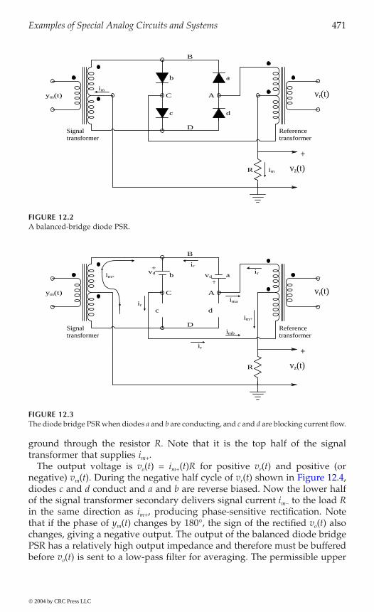
Examples of Special Analog Circuits and Systems 471
ground through the resistor R. Note that it is the top half of the signaltransformer that supplies im+.
The output voltage is vo(t) = im+(t)R for positive vr(t) and positive (orm r
diodes c and d conduct and a and b are reverse biased. Now the lower halfof the signal transformer secondary delivers signal current im- to the load Rin the same direction as im+, producing phase-sensitive rectification. Notethat if the phase of ym(t) changes by 180∞, the sign of the rectified vo(t) alsochanges, giving a negative output. The output of the balanced diode bridgePSR has a relatively high output impedance and therefore must be bufferedbefore vo(t) is sent to a low-pass filter for averaging. The permissible upper
FIGURE 12.2A balanced-bridge diode PSR.
FIGURE 12.3The diode bridge PSR when diodes a and b are conducting, and c and d are blocking current flow.
a
d
b
c
vr(t)
vz(t)
+
B
C Aym(t)
Referencetransformer
Signaltransformer
D
im
R im
R
ab
vr(t)
vz(t)
+
B
C Aym(t)
DReferencetransformer
Signaltransformer
vd
+vd
ir
ir
+ ir
im+
im+
imb
ima
c dir
© 2004 by CRC Press LLC
negative) v (t). During the negative half cycle of v (t) shown in Figure 12.4,
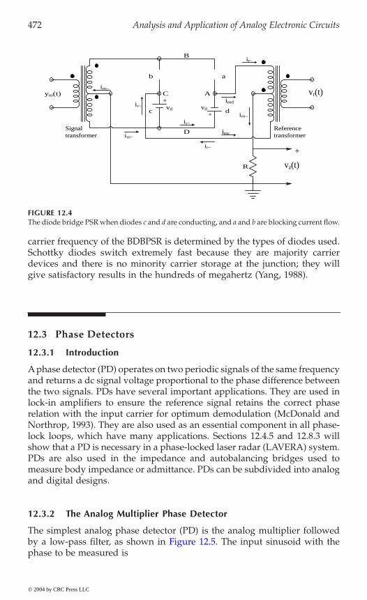
472 Analysis and Application of Analog Electronic Circuits
carrier frequency of the BDBPSR is determined by the types of diodes used.Schottky diodes switch extremely fast because they are majority carrierdevices and there is no minority carrier storage at the junction; they willgive satisfactory results in the hundreds of megahertz (Yang, 1988).
12.3 Phase Detectors
12.3.1 Introduction
A phase detector (PD) operates on two periodic signals of the same frequencyand returns a dc signal voltage proportional to the phase difference betweenthe two signals. PDs have several important applications. They are used inlock-in amplifiers to ensure the reference signal retains the correct phaserelation with the input carrier for optimum demodulation (McDonald andNorthrop, 1993). They are also used as an essential component in all phase-lock loops, which have many applications. Sections 12.4.5 and 12.8.3 willshow that a PD is necessary in a phase-locked laser radar (LAVERA) system.PDs are also used in the impedance and autobalancing bridges used tomeasure body impedance or admittance. PDs can be subdivided into analogand digital designs.
12.3.2 The Analog Multiplier Phase Detector
The simplest analog phase detector (PD) is the analog multiplier followed
phase to be measured is
FIGURE 12.4The diode bridge PSR when diodes c and d are conducting, and a and b are blocking current flow.
R
a
vr(t)
vz(t)
+
B
C A
Referencetransformer
Signaltransformer
+
ir−
ir−
dcim−+
vd vd
ir−
D imc
imd
b
ir−
im−
ym(t)im−
© 2004 by CRC Press LLC
by a low-pass filter, as shown in Figure 12.5. The input sinusoid with the

Examples of Special Analog Circuits and Systems 473
vs(t) = Vs sin(wc t + q) (12.8)
The reference sinusoid is the quadrature signal,
vr(t) = Vr cos(wc t + f) (12.9)
and the output of the analog multiplier is:
(12.10)
By trigonometric identity:
(12.11)
The LPF attenuates the 2wc frequency term; its output simply estimatesthe average:
(12.12)
Thus, for qe < 15∞,
(12.13)
where qe ∫ (q - f) is in radians.
nonlinear behavior. Because the two coherent signals must be 90∞ out ofphase for the AM PD to work, it is called a quadrature PD.
As in the case of the switched op amp PSR, it is possible to have a switchedop amp or transistor PD in which the input analog signal, vs(t), given byEquation 12.8 is effectively multiplied by a ±1 reference quadrature square
r c
the same result as the analog multiplier PD, recall that a unity square wave
FIGURE 12.5Block diagram of an analog multiplier phase detector.
Vr cos(ωc t)
Vs sin(ωc t + θ)
LPF
f0
___z(t)
z(t)1
AM
z t v t v tr s( ) = ( ) ( ) 10
z t V V tr s c( ) = ( ) + +( ) + -( ) 20 2sin sinw q f q f
z t V Vr s( ) = ( ) -( )20 sin q f
z t V Vr s c( ) @ ( )( )20 q
© 2004 by CRC Press LLC
A systems approximation for the analog multiplier PD is shown in Figure
wave given by sgnV cos(w t). To demonstrate that the switched PD gives
12.6. Note that for small phase error, the PD is linear, but exhibits periodic
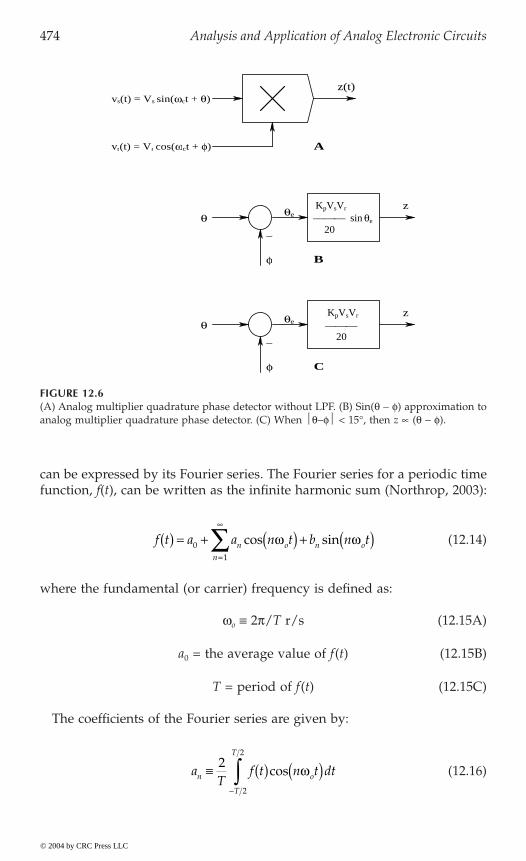
474 Analysis and Application of Analog Electronic Circuits
can be expressed by its Fourier series. The Fourier series for a periodic timefunction, f(t), can be written as the infinite harmonic sum (Northrop, 2003):
(12.14)
where the fundamental (or carrier) frequency is defined as:
wo ∫ 2p/T r/s (12.15A)
a0 = the average value of f(t) (12.15B)
T = period of f(t) (12.15C)
The coefficients of the Fourier series are given by:
(12.16)
FIGURE 12.6(A) Analog multiplier quadrature phase detector without LPF. (B) Sin(q - f) approximation toanalog multiplier quadrature phase detector. (C) When Ωq-fΩ < 15∞, then z µ (q - f).
z
z
z(t)
−
vs(t) = Vs sin(ωct + θ)
vr(t) = Vr cos(ωct + φ)
θe
−
θKpVsVr
sin θe
20
KpVsVr
20
θeθ
A
φ B
φ C
f t a a n t b n tn o n on
( ) = + ( ) + ( )=
Â01
cos sinw w
aT
f t n t dtn o
T
T
∫ ( ) ( )-Ú2
2
2
cos w
© 2004 by CRC Press LLC
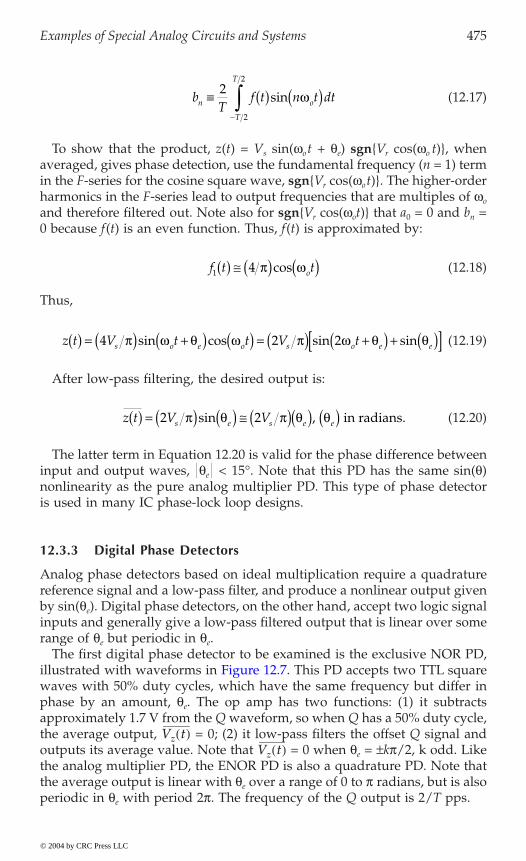
Examples of Special Analog Circuits and Systems 475
(12.17)
To show that the product, z(t) = Vs sin(wot + qe) sgnVr cos(wo t), whenaveraged, gives phase detection, use the fundamental frequency (n = 1) termin the F-series for the cosine square wave, sgnVr cos(wot). The higher-orderharmonics in the F-series lead to output frequencies that are multiples of wo
and therefore filtered out. Note also for sgnVr cos(wot) that a0 = 0 and bn =0 because f(t) is an even function. Thus, f(t) is approximated by:
(12.18)
Thus,
(12.19)
After low-pass filtering, the desired output is:
(12.20)
The latter term in Equation 12.20 is valid for the phase difference betweeninput and output waves, qe < 15∞. Note that this PD has the same sin(q)nonlinearity as the pure analog multiplier PD. This type of phase detectoris used in many IC phase-lock loop designs.
12.3.3 Digital Phase Detectors
Analog phase detectors based on ideal multiplication require a quadraturereference signal and a low-pass filter, and produce a nonlinear output givenby sin(qe). Digital phase detectors, on the other hand, accept two logic signalinputs and generally give a low-pass filtered output that is linear over somerange of qe but periodic in qe.
The first digital phase detector to be examined is the exclusive NOR PD,
waves with 50% duty cycles, which have the same frequency but differ inphase by an amount, qe. The op amp has two functions: (1) it subtractsapproximately 1.7 V from the Q waveform, so when Q has a 50% duty cycle,the average output, = 0; (2) it low-pass filters the offset Q signal andoutputs its average value. Note that = 0 when qe = ±kp/2, k odd. Likethe analog multiplier PD, the ENOR PD is also a quadrature PD. Note thatthe average output is linear with qe over a range of 0 to p radians, but is alsoperiodic in qe with period 2p. The frequency of the Q output is 2/T pps.
bT
f t n t dtn o
T
T
∫ ( ) ( )-Ú2
2
2
sin w
f t to1 4( ) @ ( ) ( )p wcos
z t V t t V ts o e o s o e e( ) = ( ) +( ) ( ) = ( ) +( ) + ( )[ ]4 2 2p w q w p w q qsin cos sin sin
z t V Vs e s e e( ) = ( ) ( ) @ ( )( ) ( )2 2p q p q qsin , in radians.
Vz t( )Vz t( )
© 2004 by CRC Press LLC
illustrated with waveforms in Figure 12.7. This PD accepts two TTL square
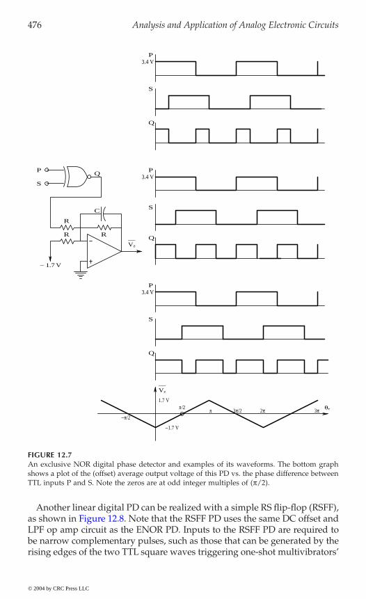
476 Analysis and Application of Analog Electronic Circuits
Another linear digital PD can be realized with a simple RS flip-flop (RSFF),
LPF op amp circuit as the ENOR PD. Inputs to the RSFF PD are required tobe narrow complementary pulses, such as those that can be generated by therising edges of the two TTL square waves triggering one-shot multivibrators’
FIGURE 12.7An exclusive NOR digital phase detector and examples of its waveforms. The bottom graphshows a plot of the (offset) average output voltage of this PD vs. the phase difference betweenTTL inputs P and S. Note the zeros are at odd integer multiples of (p/2).
− 1.7 V
R
R R
C
S
P
P
P
__Vz
3.4 V
3.4 V
3.4 V
1.7 V
−1.7 V
π 3π/2 2π 3π θe
−π/2
π/2
__Vz
Q
Q
Q
S
S
S
PQ
© 2004 by CRC Press LLC
as shown in Figure 12.8. Note that the RSFF PD uses the same DC offset and
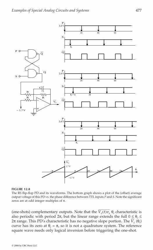
Examples of Special Analog Circuits and Systems 477
(one-shots) complementary outputs. Note that the qe characteristic isalso periodic with period 2p, but the linear range extends the full 0 £ qe £2p range. This PD’s characteristic has no negative slope portion. The (qe)curve has its zero at qe = p, so it is not a quadrature system. The referencesquare wave needs only logical inversion before triggering the one-shot.
FIGURE 12.8The RS flip-flop PD and its waveforms. The bottom graph shows a plot of the (offset) averageoutput voltage of this PD vs. the phase difference between TTL inputs P and S. Note the significantzeros are at odd integer multiples of p.
− 1.7 V
C
S
P
P
P
__Vz
3.4 V
3.4 V
3.4 V
1.7 V
−1.7 V
θe
__Vz
S
S
S
Q
2π
2π
4π
4π
2π 4π
R
6π
6π
6π
θe
θe
θe = π 3π
π 2π 3π 4π 5π−π
P __
Q
__
Q
R R __
Q
__
Q
Vz t( )vs
Vz
© 2004 by CRC Press LLC

478 Analysis and Application of Analog Electronic Circuits
More complex linear digital phase detectors have been devised. One ven-erable design based on the Motorola MC4044 IC is shown in Figure 12.9.This PD’s architecture is made up from various NAND gates. Note the two
the input and output waveforms at nodes R, V, U, and D, respectively. Thedigital waveforms for V lagging R (top set) and for V leading R (middle set)are shown. Subtracting U from D by a simple op amp DA and low-passfiltering the difference to recover the average output, , yields a linear
s e
uses a 7495 (or Fairchild 9300) four-bit, bidirectional shift register (Northrop,1990). As a PD in a PLL, it can detect lock (wp = wr) by Q0 = LO, Q2 = HI,and Q1 has the TTL phase signal similar to the RSFF output. If wp > wr, thenQ0 = LO, Q1 = LO, and Q2 has a duty cycle proportional to (wp - wr). If wp <wr, then Q1 = HI, Q2 = HI, and Q0 has a duty cycle proportional to (wr - wp).Note that this phase-frequency detector’s phase difference output on Q1 is
e p r
saturates HI when wp < wr. Q1 has a 50% duty cycle when wp = wr radians,giving (qe) = 0. Note that the P and R inputs must be narrow complemen-tary pulses derived from the`Q outputs of one-shots.
FIGURE 12.9A combinational/sequential logic PD based on the Motorola MC4044 digital PD IC.
V
R U
D
RSFF
RSFF
Vz
Vz
© 2004 by CRC Press LLC
RS flip-flops in the center of the left-hand column. Figure 12.10 illustrates
output voltage, v q , over a full ±2p interval, as shown in Figure 12.11.
not periodic in q , like other digital PDs; it saturates LO for w > w and
Another logic chip-based digital PD is shown in Figure 12.12. This circuit

Examples of Special Analog Circuits and Systems 479
Because of their linearity, digital PhDs are useful in instrumentationschemes in which phase must be measured. Note that it is possible to runtwo noise-free sinusoidal signals through comparators with hysteresis togenerate two digital signals that can be measured with a simple digital PD.
A microcomputer-based, frequency-independent digital phase meter withone-millidegree resolution was designed and tested by Du (1993) in the
FIGURE 12.10Top: example of the 4044 PD’s waveforms for V lagging R. Middle: example of the 4044 PD’swaveforms for V leading R. Bottom: op amp DA and low-pass filter used to condition the 4044PD’s outputs, U and D.
R
R
V
U
U
D
D
R1
R1 R3
CR2
R2
__VzR1
V θe
θe
DALPF
U
DVz(t)
© 2004 by CRC Press LLC
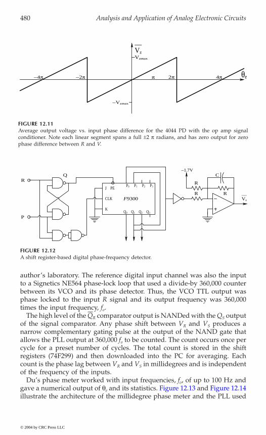
480 Analysis and Application of Analog Electronic Circuits
author’s laboratory. The reference digital input channel was also the inputto a Signetics NE564 phase-lock loop that used a divide-by 360,000 counterbetween its VCO and its phase detector. Thus, the VCO TTL output wasphase locked to the input R signal and its output frequency was 360,000times the input frequency, fo.
The high level of the QR comparator output is NANDed with the QS outputof the signal comparator. Any phase shift between VR and VS produces anarrow complementary gating pulse at the output of the NAND gate thatallows the PLL output at 360,000 fo to be counted. The count occurs once percycle for a preset number of cycles. The total count is stored in the shiftregisters (74F299) and then downloaded into the PC for averaging. Eachcount is the phase lag between VR and VS in millidegrees and is independentof the frequency of the inputs.
Du’s phase meter worked with input frequencies, fo, of up to 100 Hz ande
illustrate the architecture of the millidegree phase meter and the PLL used
FIGURE 12.11Average output voltage vs. input phase difference for the 4044 PD with the op amp signalconditioner. Note each linear segment spans a full ±2 p radians, and has zero output for zerophase difference between R and V.
FIGURE 12.12A shift register-based digital phase-frequency detector.
__Vz
θe2π 4π−2π−4π
−Vzmax
Vzmax
π
R
C
R R __Vz
−1.7V
Q0 Q1 Q2 Q3
P0 P1 P2 P3
RQ
J
K
CLK F9300
PE
P
© 2004 by CRC Press LLC
gave a numerical output of q and its statistics. Figure 12.13 and Figure 12.14
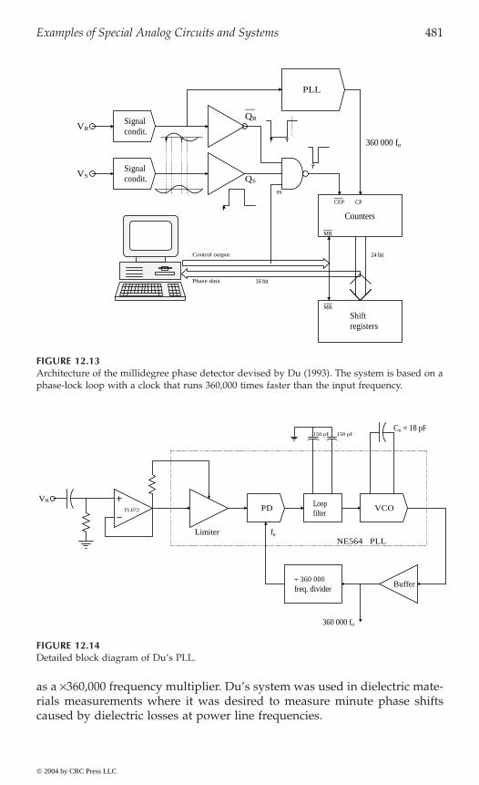
Examples of Special Analog Circuits and Systems 481
as a ¥360,000 frequency multiplier. Du’s system was used in dielectric mate-rials measurements where it was desired to measure minute phase shiftscaused by dielectric losses at power line frequencies.
FIGURE 12.13Architecture of the millidegree phase detector devised by Du (1993). The system is based on aphase-lock loop with a clock that runs 360,000 times faster than the input frequency.
FIGURE 12.14Detailed block diagram of Du’s PLL.
__CEP CP
Counters
24 bit
16 bit
Shiftregisters
360 000 fo
VRSignalcondit.
Signalcondit.
VS
__QR
QS
PLL
__MR
__MR
Phase data
Control output
en
VCO
Co = 18 pF
Buffer
Loopfilter
PD
150 pF150 pF
÷ 360 000freq. divider
foNE564
Limiter
VR
TL072
PLL
360 000 fo
© 2004 by CRC Press LLC
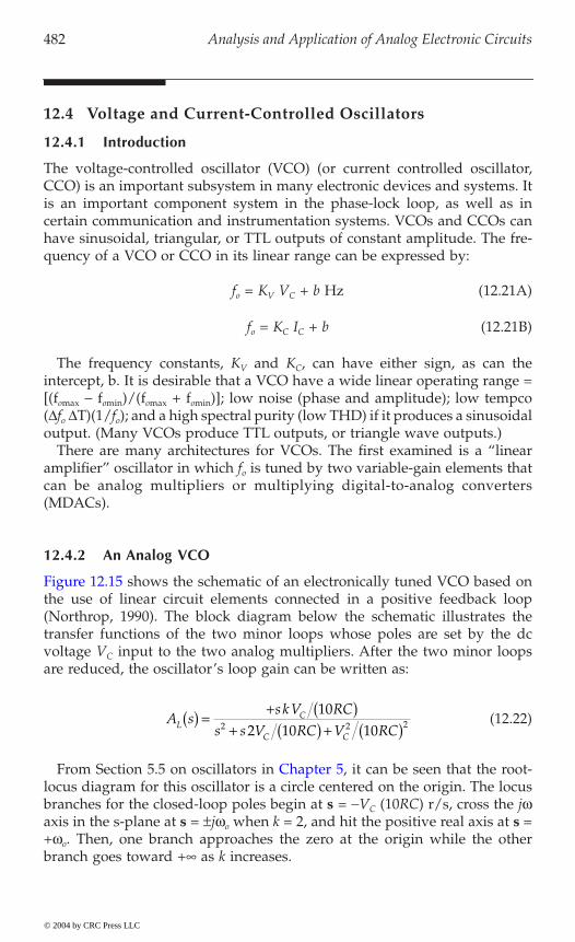
482 Analysis and Application of Analog Electronic Circuits
12.4 Voltage and Current-Controlled Oscillators
12.4.1 Introduction
The voltage-controlled oscillator (VCO) (or current controlled oscillator,CCO) is an important subsystem in many electronic devices and systems. Itis an important component system in the phase-lock loop, as well as incertain communication and instrumentation systems. VCOs and CCOs canhave sinusoidal, triangular, or TTL outputs of constant amplitude. The fre-quency of a VCO or CCO in its linear range can be expressed by:
fo = KV VC + b Hz (12.21A)
fo = KC IC + b (12.21B)
The frequency constants, KV and KC, can have either sign, as can theintercept, b. It is desirable that a VCO have a wide linear operating range =[(fomax - fomin)/(fomax + fomin)]; low noise (phase and amplitude); low tempco(Dfo DT)(1/fo); and a high spectral purity (low THD) if it produces a sinusoidaloutput. (Many VCOs produce TTL outputs, or triangle wave outputs.)
There are many architectures for VCOs. The first examined is a “linearamplifier” oscillator in which fo is tuned by two variable-gain elements thatcan be analog multipliers or multiplying digital-to-analog converters(MDACs).
12.4.2 An Analog VCO
the use of linear circuit elements connected in a positive feedback loop(Northrop, 1990). The block diagram below the schematic illustrates thetransfer functions of the two minor loops whose poles are set by the dcvoltage VC input to the two analog multipliers. After the two minor loopsare reduced, the oscillator’s loop gain can be written as:
(12.22)
locus diagram for this oscillator is a circle centered on the origin. The locusbranches for the closed-loop poles begin at s = -VC (10RC) r/s, cross the jwaxis in the s-plane at s = ±jwo when k = 2, and hit the positive real axis at s =+wo. Then, one branch approaches the zero at the origin while the otherbranch goes toward + as k increases.
A sskV RC
s s V RC V RCLC
C C
( ) =+ ( )
+ ( ) + ( )10
2 10 102 2 2
© 2004 by CRC Press LLC
Figure 12.15 shows the schematic of an electronically tuned VCO based on
From Section 5.5 on oscillators in Chapter 5, it can be seen that the root-

Examples of Special Analog Circuits and Systems 483
Using the venerable Barkhausen criterion (Millman, 1979) for oscillationon this oscillator:
(12.23)
Clearly, the real terms in the denominator must sum to zero. This conditiongives the radian oscillation frequency,
(12.24)
FIGURE 12.15Schematic of a voltage-tuned oscillator using positive feedback. The tungsten filament lamp isused to limit and stabilize oscillation amplitude. A systems block diagram of the linear part ofthe oscillator is shown below the schematic. See text for analysis.
kR
RRR
R
R
R
R
VC > 0
−
−
AM1
AM2
V1
V2 V3 V4
V5
V6
V7
s
s + VC /(10RC)
s + VC /(10RC)
V1’
+
+
R C
C
C
− VC /(10RC)V4
− kV5
V1
V1’
R + αV4
AL jj kV RC
V RC j V RCoo C
o C o C
ww
w w( ) ∫ ∞ = ( )
- + ( ) + ( )1 0
1010 2 102 2 2
wo CV RC= ( )10 r s ,
© 2004 by CRC Press LLC

484 Analysis and Application of Analog Electronic Circuits
and the minimum gain for oscillation, k = 2. Thus, VC can set wo over a widerange, e.g., 0.01 £ VC £ 10 V, or a 1:1000 range. For practical reasons, makek > 2 and use a PTC tungsten lamp instead of the input R to the third op amp.Now the overall gain of this stage is:
(12.25)
If k = 4 is set, then the steady state, equilibrium value of V4 is found to beR/a for any wo. Making k = 4 allows the oscillations to grow rapidly to theequilibrium level.
12.4.3 Switched Integrating Capacitor VCOs
Certain VCOs can simultaneously output TTL pulses, a triangle wave, anda sine wave of the same frequency. An example of this type of VCO is theExar XR8038 waveform generator, which works over a range of millihertzto approximately 1 MHz with proper choice of timing capacitor, CT. A newerversion of the XR8038 is the Maxim MAX038 VFC, which can generatevarious waveforms from 1 mHz to 20 MHz.
capacitor VCO. Assume that Vin > 0. At t = 0, the MOS switch is in positionu and the capacitor is charged by current GmVin, so VT goes from 0 to VT =f+ when the output of the upper comparator goes HI, which makes the RSflip-flop Q output go HI, causing the MOS switch to go to position d. Inposition d, the capacitor CT is discharged by a net current, -GmVin, causingVT to ramp down to f- < 0. When VT reaches f-, the output of the lowercomparator goes high, causing the RSFF Q output to go LO, which switchesthe MOS switch to u again, causing the capacitor to charge positively againfrom current GmVin, etc.
Vin is the controlling input to the two VCCSs. Note that the capacitor CT
integrates the current:
(12.26)
Thus, from the VT triangle waveform, it is easy to find the frequency ofoscillation:
(12.27)
In Equation 12.27, f = f+ = -f- > 0 was assumed.
VV
k RR V
5
4 4
2= -+
= -a
V C i dtT T C= ( ) Ú1
f TG V
Cm in
T
= =14 f
Hz
© 2004 by CRC Press LLC
Figure 12.16 illustrates the organization of a generic switched integrating

Examples of Special Analog Circuits and Systems 485
Note that this VCO produces simultaneous sine, triangle, and TTL outputs.The sinusoidal output is derived from the buffered capacitor waveform, VT,by passing it through a diode wave-shaper, sin(*) NL. This type of VCO isoften used as the basis for laboratory function generators.
12.4.4 The Voltage-Controlled, Emitter-Coupled Multivibrator
architecture. This astable, emitter-coupled multivibrator (AMV) derives itsfrequency control from the transistors Q5 and Q6, which act as VCCSs andcontrol the rate that CT charges and discharges and, thus, the AMV’s fre-quency. This architecture is inherently very fast; versions of it using MOSFETshave been used to build a VCO with an 800-MHz tuning range that operatesin excess of 2.5 GHz (Herzel et al., 2001).
The heart of this VCO is the free-running, astable multivibrator (AMV),which alternately switches Q1 and Q2 on and off as the timing capacitorcharges and discharges. Detailed analysis of this circuit can be found in
FIGURE 12.16Block diagram of a switched integrating capacitor VCO.
2GmVin
CT× 1 Buff
VT
S
RSFF
× 1 Buffφ+
Comp.
Comp.
φ−
φ+
t
MOS SW to dVT
MOS SW to u
d
u
MOS SW
Triangle out
VT QRGmVin TTL out
Vcc
Vin
VCCS
VCCS
φ− < 0
0 T/4 T
Sine out
sin(*) NL
© 2004 by CRC Press LLC
Figure 12.17 illustrates the simplified schematic of another popular VCO
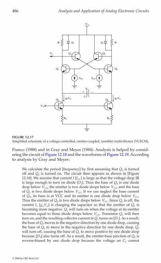
486 Analysis and Application of Analog Electronic Circuits
Franco (1988) and in Gray and Meyer (1984). Analysis is helped by consid-
to analysis by Gray and Meyer:
We calculate the period [frequency] by first assuming that Q1 is turnedoff and Q2 is turned on. The circuit then appears as shown in [Figure12.18]. We assume that current I [Ic2 ] is large so that the voltage drop IRis large enough to turn on diode [D2]. Thus the base of Q4 is one diodedrop below VCC, the emitter is two diode drops below VCC, and the baseof Q1 is two diode drops below VCC. If we can neglect the base currentof Q3, its base is at VCC and its emitter is one diode drop below VCC.Thus the emitter of Q2 is two diode drops below VCC. Since Q1 is off, thecurrent I1 [gmVin] is charging the capacitor so that the emitter of Q1 isbecoming more negative. Q1 will turn on when the voltage at its emitterbecomes equal to three diode drops below VCC. Transistor Q1 will thenturn on, and the resulting collector current in Q1 turns on [D1]. As a result,the base of Q3 moves in the negative direction by one diode drop, causingthe base of Q2 to move in the negative direction by one diode drop. Q2
will turn off, causing the base of Q1 to move positive by one diode dropbecause [D2] also turns off. As a result, the emitter-base junction of Q2 isreverse-biased by one diode drop because the voltage on CT cannot
FIGURE 12.17Simplified schematic of a voltage-controlled, emitter-coupled, (astable) multivibrator (VCECM).
gmVin
Q1 Q2
Q3 Q4
Q6
RE RE
Vin
Ibias Ibias
Vo
VC
+ −
gmVinCT
D1R D2 R
Vcc
Q5
© 2004 by CRC Press LLC
ering the circuit of Figure 12.18 and the waveforms of Figure 12.19. According
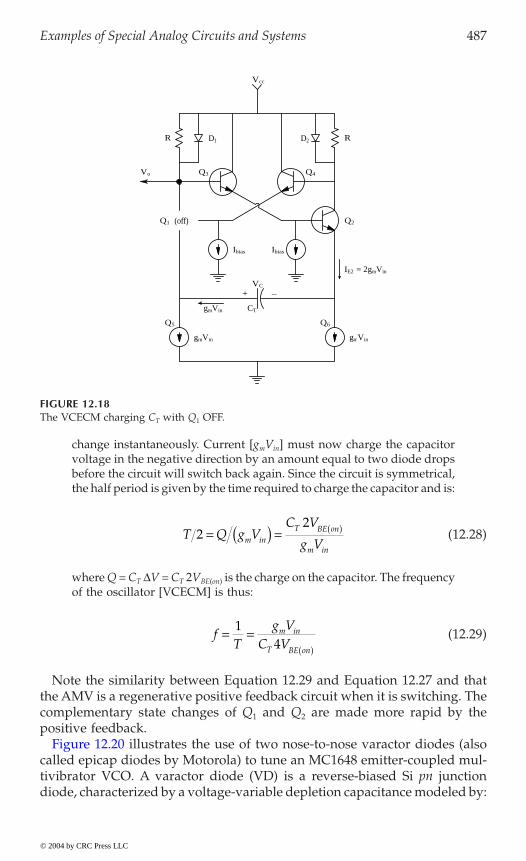
Examples of Special Analog Circuits and Systems 487
change instantaneously. Current [gmVin] must now charge the capacitorvoltage in the negative direction by an amount equal to two diode dropsbefore the circuit will switch back again. Since the circuit is symmetrical,the half period is given by the time required to charge the capacitor and is:
(12.28)
where Q = CT DV = CT 2VBE(on) is the charge on the capacitor. The frequencyof the oscillator [VCECM] is thus:
(12.29)
Note the similarity between Equation 12.29 and Equation 12.27 and thatthe AMV is a regenerative positive feedback circuit when it is switching. Thecomplementary state changes of Q1 and Q2 are made more rapid by thepositive feedback.
called epicap diodes by Motorola) to tune an MC1648 emitter-coupled mul-tivibrator VCO. A varactor diode (VD) is a reverse-biased Si pn junctiondiode, characterized by a voltage-variable depletion capacitance modeled by:
FIGURE 12.18The VCECM charging CT with Q1 OFF.
Q1 Q2
Q3 Q4
Ibias Ibias
Vo
VC
+ −
CT
D1R D2 R
Vcc
(off)
gmVin
Q5 Q6
IE2 = 2gmVin
gmVin
gmVin
T Q g VC V
g Vm inT BE on
m in
22
= ( ) = ( )
fT
g VC V
m in
T BE on
= =( )
14
© 2004 by CRC Press LLC
Figure 12.20 illustrates the use of two nose-to-nose varactor diodes (also

488 Analysis and Application of Analog Electronic Circuits
(12.30)
where Cvo is the diode’s junction capacitance at VD = 0, yo is the “built-inbarrier potential,” typically on the order of 0.75 V for a Si diode at roomtemperature, and g is the capacitance exponent. g can vary from approxi-mately 1/3 to 2, depending on the doping gradients at the junction boundaryand can be shown to be @ 0.5 for an abrupt (step) junction (Gray and Meyer,1984).
The output of the MC1648 oscillator is an emitter-coupled logic (ECL)square wave; frequencies as high as 225 MHz can be obtained with this IC,
FIGURE 12.19Relevant waveforms in the VCECM for two cycles of oscillation.
Vb2
Vcc
Vcc − 2VBE
Vcc − VBE
VBE ≅ 0.6 Vt
0
Ve2
Vcc
Vcc − VBE
Vcc − 2VBE
Vcc − 3VBE
0
VC
0
0.6
−0.6
Vo (VC3)
Vcc
Q1 OFF Q2 OFF Q1 OFFVcc − VBE
0
CC
VVv
vo
D o
D=-( )
<1
0y
g , .
© 2004 by CRC Press LLC

Examples of Special Analog Circuits and Systems 489
which can serve as the VCO in a PLL. In the circuit shown, the tuning rangelies between VD = -2 to –10 V (or 2 £ Vc £ 10 V). The actual fo(Vc) curve issigmoid, but can be approximated by the linear VCO relation,
fo @ 15Vc + 20 MHz, (12.31)
over the range of Vc shown. Note that two VDs are used in series to halvetheir capacitance, seen in the resonant “tank” circuit. A Motorola MV1404VD’s capacitance goes from 160 pF at VD = -1 to approximately 11 pF atVD = -10 V.
FIGURE 12.20Top: A VCO that uses the voltage-variable capacitance of two varactor diodes to set its outputfrequency. Bottom: The frequency vs. dc control voltage characteristic of the varactor VCO.
L
L = 5 T #20 Cu wire onMicroMetal #T30-13toroidal core
Vc
51 kΩ
VD
VD
VD = MV1404varactor diode
Vo
5 µF 0.1 µF
0.1 µF
Vc
fo (MHz)
110
90
70
130
150
170
50100 2 864
fo ≅ 15Vc + 20 MHz, (2 ≤ Vc ≤ 10 V)
MC1648 ECO
© 2004 by CRC Press LLC

490 Analysis and Application of Analog Electronic Circuits
12.4.5 The Voltage-to-Period Converter and Applications
The voltage-to-period converter (VPC) is a variable frequency oscillator inwhich the period of the oscillation, T, is directly proportional to the control-ling voltage, Vc. Mathematically, this is simply stated as:
T = KP Vc + b seconds (12.32)
Here b is a positive constant and KP is the VPC constant in seconds pervolt. Practical considerations dictate lower and upper bounds to T. Obviously,the VPC’s output frequency is 1/T Hz. The conventional voltage-to-frequencyconverter (VFC) has its output frequency directly proportional to its inputvoltage (or current),
fo = KV Vc + d (12.33)
KV is the VCO constant in Hertz per volt and d is a constant (Hertz).In several important instrumentation applications, use of a VPC (rather
than a VFC) linearizes the measurement system output; several examplesare described next.
Realization of VPCs. As has been shown, many IC manufacturers makeVFC VCOs. Some have TTL outputs; others generate sine, triangle, and TTLoutputs. No one, to this author’s knowledge, markets a VPC IC. One obviousway to make a VPC is to take a VFC in which fo = KVVc + d and use a nonlinearanalog circuit to process the input, V1, so that the net result is a VPC.Mathematically,
(12.34)
To find the required nonlinearity, solve Equation 12.34 for V2 = f (V1). Thisgives:
(12.35)
Considerable simplification accrues if a VFC with d = 0 is used. Now thenonlinearity needs to be:
(12.36)
V2 for the VFC to produce a VPC. Note that V3 must be >0 and VR = +0.1 V.
T K V bK V dP
V
= + =+1
2
1
Vbd d K V
K K V bP
V P2
1
1
1= - -+( )
VK K V bV P
21
1=+( )
© 2004 by CRC Press LLC
Figure 12.21 illustrates an op amp circuit that will generate the requisite
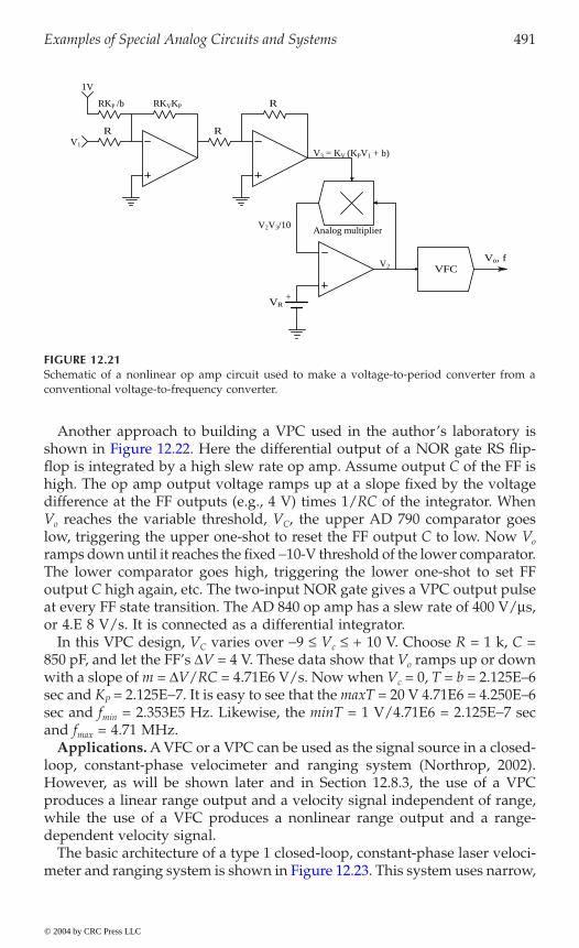
Examples of Special Analog Circuits and Systems 491
Another approach to building a VPC used in the author’s laboratory is
flop is integrated by a high slew rate op amp. Assume output C of the FF ishigh. The op amp output voltage ramps up at a slope fixed by the voltagedifference at the FF outputs (e.g., 4 V) times 1/RC of the integrator. WhenVo reaches the variable threshold, VC, the upper AD 790 comparator goeslow, triggering the upper one-shot to reset the FF output C to low. Now Vo
ramps down until it reaches the fixed -10-V threshold of the lower comparator.The lower comparator goes high, triggering the lower one-shot to set FFoutput C high again, etc. The two-input NOR gate gives a VPC output pulseat every FF state transition. The AD 840 op amp has a slew rate of 400 V/ms,or 4.E 8 V/s. It is connected as a differential integrator.
In this VPC design, VC varies over -9 £ Vc £ + 10 V. Choose R = 1 k, C =850 pF, and let the FF’s DV = 4 V. These data show that Vo ramps up or downwith a slope of m = DV/RC = 4.71E6 V/s. Now when Vc = 0, T = b = 2.125E–6sec and KP = 2.125E-7. It is easy to see that the maxT = 20 V 4.71E6 = 4.250E–6sec and fmin = 2.353E5 Hz. Likewise, the minT = 1 V/4.71E6 = 2.125E-7 secand fmax = 4.71 MHz.
Applications. A VFC or a VPC can be used as the signal source in a closed-loop, constant-phase velocimeter and ranging system (Northrop, 2002).However, as will be shown later and in Section 12.8.3, the use of a VPCproduces a linear range output and a velocity signal independent of range,while the use of a VFC produces a nonlinear range output and a range-dependent velocity signal.
The basic architecture of a type 1 closed-loop, constant-phase laser veloci-
FIGURE 12.21Schematic of a nonlinear op amp circuit used to make a voltage-to-period converter from aconventional voltage-to-frequency converter.
R
R
R
VR
V2V3/10
V3 = KV (KPV1 + b)
1V
V1
V2
Analog multiplier
+
VFC
RKP /b RKVKP
Vo, f
© 2004 by CRC Press LLC
shown in Figure 12.22. Here the differential output of a NOR gate RS flip-
meter and ranging system is shown in Figure 12.23. This system uses narrow,
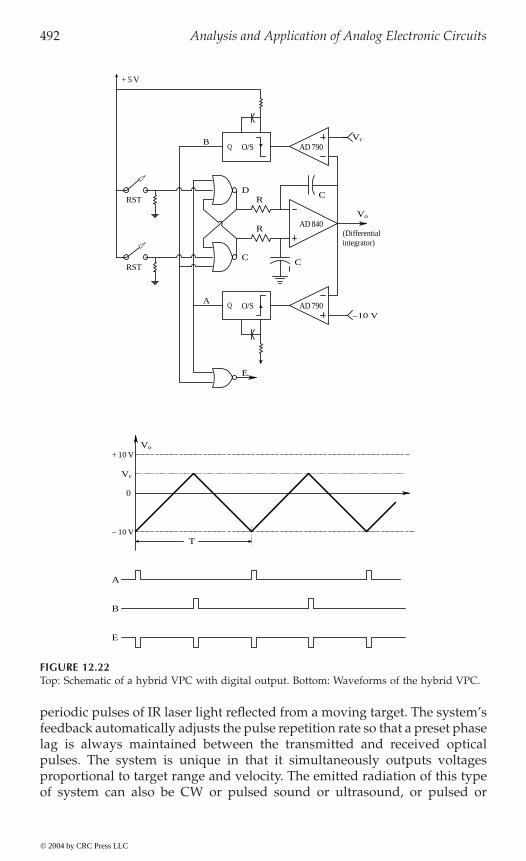
492 Analysis and Application of Analog Electronic Circuits
periodic pulses of IR laser light reflected from a moving target. The system’sfeedback automatically adjusts the pulse repetition rate so that a preset phaselag is always maintained between the transmitted and received opticalpulses. The system is unique in that it simultaneously outputs voltagesproportional to target range and velocity. The emitted radiation of this typeof system can also be CW or pulsed sound or ultrasound, or pulsed or
FIGURE 12.22Top: Schematic of a hybrid VPC with digital output. Bottom: Waveforms of the hybrid VPC.
QA
Vc
−10 VAD 790
AD 840
QB
AD 790O/S
O/S
R
R
C
C
Vo
C
D
E
+ 5 V
Vo
+ 10 V
− 10 V
Vc
0
T
E
A
B
RST
RST
(Differentialintegrator)
© 2004 by CRC Press LLC
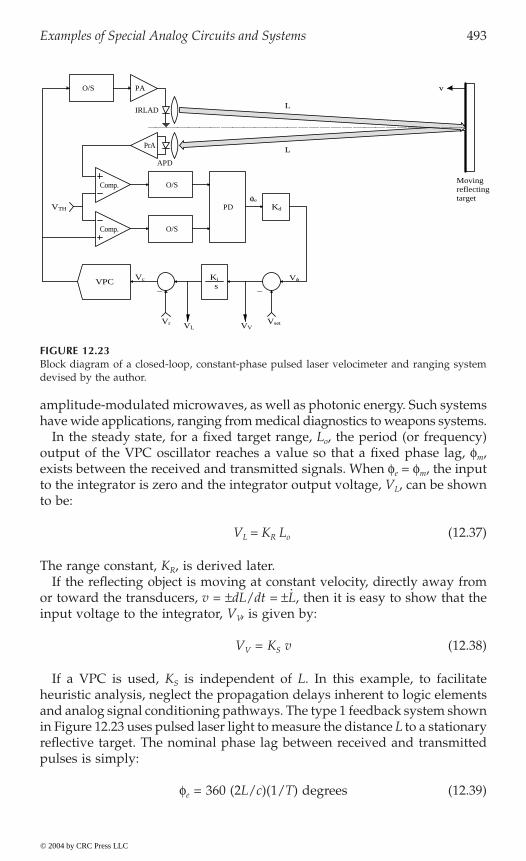
Examples of Special Analog Circuits and Systems 493
amplitude-modulated microwaves, as well as photonic energy. Such systemshave wide applications, ranging from medical diagnostics to weapons systems.
In the steady state, for a fixed target range, Lo, the period (or frequency)output of the VPC oscillator reaches a value so that a fixed phase lag, fm,exists between the received and transmitted signals. When fe = fm, the inputto the integrator is zero and the integrator output voltage, VL, can be shownto be:
VL = KR Lo (12.37)
The range constant, KR, is derived later.If the reflecting object is moving at constant velocity, directly away from
or toward the transducers, v = ±dL/dt =·±L, then it is easy to show that the
input voltage to the integrator, VV, is given by:
VV = KS v (12.38)
If a VPC is used, KS is independent of L. In this example, to facilitateheuristic analysis, neglect the propagation delays inherent to logic elementsand analog signal conditioning pathways. The type 1 feedback system shownin Figure 12.23 uses pulsed laser light to measure the distance L to a stationaryreflective target. The nominal phase lag between received and transmittedpulses is simply:
fe = 360 (2L/c)(1/T) degrees (12.39)
FIGURE 12.23Block diagram of a closed-loop, constant-phase pulsed laser velocimeter and ranging systemdevised by the author.
IRLAD
PAO/S
O/S
PD Kd
Comp.
Comp.
s
PrA
VTH
Vr VsetVL VV
φe
L
L
O/SMovingreflectingtarget
v
KiVPCVc Vφ
APD
− −
© 2004 by CRC Press LLC
494 Analysis and Application of Analog Electronic Circuits
where c is the velocity of light in m/s, T is the VPC output period, and (2L/c)is the round-trip time for a pulse reflected from the target. The phase detectormodule produces an output voltage with an average value of:
Vf = Kd fe (12.40)
Kd has the dimensions of volts per degree. A dc voltage, Vset, is subtractedfrom Vf, so:
VV = Vf - Vset (12.41)
VV is the input to the integrator whose output, VL , is added to -Vr to givethe input to the VPC, VC. Because the closed-loop system is type 1, in thesteady state, VV Æ 0. Thus,
(12.42)
Thus, the steady-state phase lag is simply:
fe = fm = Vset Kd degrees (12.43)
The VPC steady-state period is found from Equation 12.42 to be:
(12.44)
From the preceding equation, the VPC input voltage is:
(12.45)
If Vr = b/KP, then VL is directly proportional to L:
(12.46)
Now consider the situation in which the reflecting target is approachingthe transducers at constant velocity, v c. Because VL = (Ki s) VV and v =
·L, it
is possible to write in the time domain:
(12.47)
Thus, a simple type 1 closed-loop, constant phase system can providesimultaneous voltage outputs that estimate target range and velocity in alinear manner.
V K K L c T K L c fset d m d d= = ( )( )[ ] = ( )[ ]f 360 2 1 360 2
T K V bL
css P Cmss
= + = 720f
seconds
VL
c Kb KC
mss PP= -720
f volts
Vc K V K
LLP set d
= ( )720
volts.
V V K vK
c K V KV o id
P set i
= =˙ 720 volts
© 2004 by CRC Press LLC

Examples of Special Analog Circuits and Systems 495
Examine the system design with practical numbers: let fm ∫ 10º; Ki = 1 andKP = 8.0E-6 sec/V; and 720/c = 2.40E-6. These numbers give a reasonablerange sensitivity:
(12.48)
From Equation 12.47, the velocity sensitivity is also useful:
(12.49)
The VPC steady-state output frequency at a 1-m range is 4.17 MHz; whenL = 100 m, it is 41.7 kHz.
12.4.6 Summary
There are a variety of architectures for voltage-controlled oscillators, including“linear” VCOs using variable gain elements, switched integrating capacitorVCOs, and emitter-coupled, astable multivibrators. Versions of the latterarchitecture have been made to oscillate in the gigahertz. Another VHF–UHFVCO architecture (not shown here) makes use of the varactor diode (VD).The VD is a reverse-biased pn junction diode in which the diode depletioncapacitance is controlled by the reverse-bias voltage. This voltage-variablecapacitance can be used to tune oscillators such as the familiar Hartley designand to generate NBFM by adding the modulating signal to the reverse diodebias voltage. VCOs are used in all phase-lock loops and in FM communica-tions applications, as well as in many instrumentation systems.
The voltage-to-period converter (VPC) is a VCO in which the outputoscillation’s period is linearly proportional to the input voltage. The VPC isa useful circuit component in a closed-loop, constant-phase laser velocimeterand ranging system. The same closed-loop, constant-phase architecture canalso be used with sound or ultrasound to measure object range and velocitysimultaneously.
12.5 Phase-Locked Loops
12.5.1 Introduction
A phase-locked loop (PLL) (also called a phase-lock loop) is a closed-loopfeedback system in which the phase of the PLL’s periodic output is made tofollow the phase of a periodic input signal. The closed-loop PLL system’s
Kc KR
P mss
= = -7203 0 2
f. E V m
KK KS
P mss i
= - = -2 40 61
3 0 2. .E E V m sf
© 2004 by CRC Press LLC

496 Analysis and Application of Analog Electronic Circuits
natural frequencies are, in general, several orders of magnitude lower thanthe frequency of the input signal. Phase-lock loops have many applicationsin communications, control systems, and instrumentation systems. They canbe used to modulate and demodulate narrow-band FM (NBFM) signals;demodulate double-sideband/suppressed carrier (DSBSC) signals; demod-ulate AM signals; generate a frequency-independent phase shift; measurefrequencies, including heart rate; synthesize signals used in digital commu-nications systems; detect touch-tone frequencies and status signals used intelephony; control motor speed, etc.
The basic architecture of a PLL is shown in Figure 12.24(A). It includes aphase (difference) detector (PD), loop filter, VCO (VFC), and, sometimes, afrequency divider between the VCO and the PD. (Phase detectors weredescribed in Section 12.3.) A phase detector returns an average voltage pro-portional to the phase difference between the input signal and the VCOoutput.
Analysis of PLL dynamics is done assuming lock, i.e., that the input andVCO frequencies are equal. When a PLL first acquires its input signal, f1 π fo
and the loop must attain lock through a nonlinear process known as acqui-sition. The time required for acquisition is important in such PLL applica-tions as telephone touch-tone decoding and the demodulation of FSK signals.Empirical formulas for acquisition times can be found in Northrop (1990)and Gardner (1979).
FIGURE 12.24(A) Basic architecture of a phase-locked loop (PLL). (B) Systems block diagram of a PLL.
÷ N
N f1
PDLoopfilter
VCOVcVφf1
Freq. divider
fo = f1
θo
θ1
Vφ ∝ (θ1 − θo)
@ lock:
s
θo
Loop filterVCO
−
Linearized PD
A
B
θ1 θe
Kp
VφF(s)
Vc Kvθo, fo
fo = f1 at lock
© 2004 by CRC Press LLC
Examples of Special Analog Circuits and Systems 497
12.5.2 PLL Components
As mentioned earlier, phase detectors such as those used in PLLs havealready been considered in Section 12.3. Most IC PLLs use PDs in which theanalog input signal is effectively multiplied by a ±1 square wave derivedfrom the VCO. This type of PD is a quadrature detector; the zero phase errorcondition requires that q1 - qo = p/2. Analog multiplier and exclusive ORPDs are also quadrature detectors. Only the RSFF PD and the MC 4044 PDare in-phase detectors.
All PDs produce an analog output whose average value, Vf, is proportionalto sin(qe) or to qe. When qe < 15º, sin(qe) can be replaced with qe in radians.Thus, for small-signal errors at lock, the PLL can be modeled by the block
by Kv s because wo = Vc Kv r/s and its output phase is, in general, the integralof its output frequency, i.e., qo = Ú wo dt. The PLL’s dynamics in response tochanges in q1 are determined in part by its closed-loop poles, which can befound from its linear loop gain using root-locus techniques. The PLL’s loopgain is generally:
(12.50)
If F(s) = Kf (s + a)/s, then the loop gain function has a zero at s = -a, andtwo poles at the origin. Its root-locus is the well-known circle, shown in
-a ± ja. This gives a damping factor of x = 0.707 and an undamped naturalfrequency of wn = a÷2. The scalar gain product, Kp Kf Kv, is adjusted to obtainthese closed-loop parameters. It can be shown that Kp Kf Kv = 2a will put theclosed-loop poles at s = -a ± ja (Northrop, 1990).
The PLL’s loop filter is generally low-pass and can be of the form F(s) =Kf (s/b + 1), Kf (s + a)/s, Kf (s/a + 1)/(s/b + 1), etc. The loop filter is generallychosen to give the PLL the desired dynamic response in tracking changes in
1
used on IC PLLs often uses the voltage-controlled, emitter-coupled astablemultivibrator architecture (see above).
12.5.3 PLL Applications in Biomedicine
illustrates the block diagram of a 4046 CMOS PLL used as a cardiotachometer(Northrop, 1990). The loop filter’s transfer function is found from the voltage-divider relation:
(12.51)
A sK F s K
sLp v( ) =
( )
VV
R sCR R sC
sCRsC R R
c
f
= ++ +
= ++( ) +
2
1 2
2
1 2
11
11
© 2004 by CRC Press LLC
diagram in Figure 12.24(B). The VCO is modeled in the frequency domain
Figure 12.25. Effective design of this PLL wants the closed-loop poles at s =
q . The PLL’s VCO can have a digital (TTL) or sinusoidal output. The VCO
One application of a PLL is its use to measure heart rate. Figure 12.26

498 Analysis and Application of Analog Electronic Circuits
Similarly, the output transfer function is:
(12.52)
and the PLL’s loop gain is:
FIGURE 12.25Root-locus diagram of a PLL having a loop filter of the form, F(s) = Kf (s + a)/s.
FIGURE 12.26Block diagram of a PLL used as a heart rate monitor. Vo is proportional to the average heart rate.
ωn = a√2
−a
ja
jω
σ
s-plane
−2a
PD
Kv
s
VCO
÷ N
R1
R2
C
Vo
Vc
θo
ωo Nωo
Loopfilter
Kp
−
θi Vφ×1
2πs (rad) +
f1
(beat/s)
VV
sCR R sC sC R R
o
f
=+ +
=+( ) +
11
111 2 1 2
© 2004 by CRC Press LLC
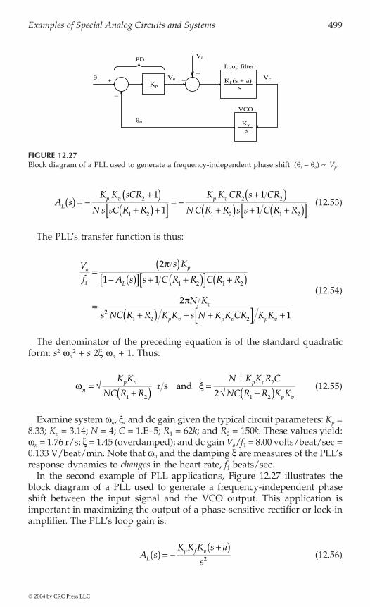
Examples of Special Analog Circuits and Systems 499
(12.53)
The PLL’s transfer function is thus:
(12.54)
The denominator of the preceding equation is of the standard quadraticform: s2 wn
2 + s 2x wn + 1. Thus:
(12.55)
Examine system wn, x, and dc gain given the typical circuit parameters: Kp =8.33; Kv = 3.14; N = 4; C = 1.E-5; R1 = 62k; and R2 = 150k. These values yield:wn = 1.76 r/s; x = 1.45 (overdamped); and dc gain Vo/f1 = 8.00 volts/beat/sec =0.133 V/beat/min. Note that wn and the damping x are measures of the PLL’sresponse dynamics to changes in the heart rate, f1 beats/sec.
In the second example of PLL applications, Figure 12.27 illustrates theblock diagram of a PLL used to generate a frequency-independent phaseshift between the input signal and the VCO output. This application isimportant in maximizing the output of a phase-sensitive rectifier or lock-inamplifier. The PLL’s loop gain is:
(12.56)
FIGURE 12.27Block diagram of a PLL used to generate a frequency-independent phase shift. (qi - qo) µ Vp.
s
sKv
VCO
Loop filter
+ ++
−
Kp
VpPD
θ1 Vφ Kf (s + a) Vc
θo
A sK K sCR
N s sC R R
K K CR s CR
N C R R s s C R RLp v p v( ) = -
+( )+( ) +[ ] = -
+( )+( ) + +( )[ ]
2
1 2
2 2
1 2 1 2
1
1
1
1
Vf
s K
A s s C R R C R R
N K
s NC R R K K s N K K CR K K
o p
L
v
p v p v p v
1 1 2 1 2
21 2 2
2
1 1
2
1
=( )
- ( )[ ] + +( )[ ] +( )
=+( ) + +[ ] +
p
p
w xnp v p v
p v
K K
NC R R
N K K R C
NC R R K K= ÷
+( ) =+
÷ +( )1 2
2
1 22 r s and
A sK K K s a
sLp f v( ) = -
+( )2
© 2004 by CRC Press LLC
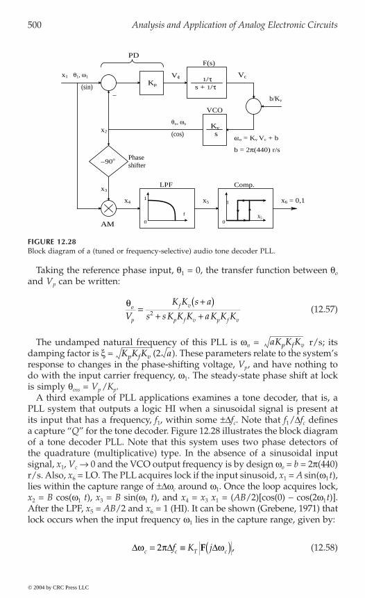
500 Analysis and Application of Analog Electronic Circuits
Taking the reference phase input, q1 = 0, the transfer function between qo
and Vp can be written:
(12.57)
The undamped natural frequency of this PLL is wn = r/s; itsdamping factor is x = (2 ). These parameters relate to the system’sresponse to changes in the phase-shifting voltage, Vp, and have nothing todo with the input carrier frequency, w1. The steady-state phase shift at lockis simply qoss = Vp /Kp.
A third example of PLL applications examines a tone decoder, that is, aPLL system that outputs a logic HI when a sinusoidal signal is present atits input that has a frequency, f1, within some ±Dfc. Note that f1/Dfc definesa capture “Q” for the tone decoder. Figure 12.28 illustrates the block diagramof a tone decoder PLL. Note that this system uses two phase detectors ofthe quadrature (multiplicative) type. In the absence of a sinusoidal inputsignal, x1, Vc Æ 0 and the VCO output frequency is by design wo = b = 2p(440)r/s. Also, x6 = LO. The PLL acquires lock if the input sinusoid, x1 = A sin(w1t),lies within the capture range of ±Dwc around w1. Once the loop acquires lock,x2 = B cos(w1 t), x3 = B sin(w1 t), and x4 = x3 x1 = (AB/2)[cos(0) - cos(2w1t)].After the LPF, x5 = AB/2 and x6 = 1 (HI). It can be shown (Grebene, 1971) thatlock occurs when the input frequency w1 lies in the capture range, given by:
(12.58)
FIGURE 12.28Block diagram of a (tuned or frequency-selective) audio tone decoder PLL.
s + 1/τ
PDF(s)
Phaseshifter
−90o
AM
LPF Comp.
x2
x3
x6 = 0,1x5 1
0x5
f
x41
0
(cos)
1/τVφx1
Kp(sin)
θ1, ω1
θo, ωo
VCO
sKv
Vc
b/Kv−
ωo = Kv Vc + b
b = 2π(440) r/s
qo
p
f v
p f v p f vV
K K s a
s sK K K aK K K=
+( )+ +2
aKpKfKvKpKfKv a
D D Dw p wc c T cf K j= ∫ ( )2 F ,
© 2004 by CRC Press LLC
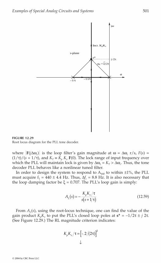
Examples of Special Analog Circuits and Systems 501
where F(jDwc) is the loop filter’s gain magnitude at w = Dwc r/s, F(s) =(1/t)/(s + 1/t), and KT ∫ Kp Kv F(0). The lock range of input frequency overwhich the PLL will maintain lock is given by DwL = KT > Dwc. Thus, the tonedecoder PLL behaves like a nonlinear tuned filter.
In order to design the system to respond to A440 to within ±1%, the PLLmust acquire f1 = 440 ± 4.4 Hz. Thus, Dfc = 8.8 Hz. It is also necessary thatthe loop damping factor be x = 0.707. The PLL’s loop gain is simply:
(12.59)
From AL(s), using the root-locus technique, one can find the value of thegain product KpKv to put the PLL’s closed loop poles at s* = -1/2t ± j 2t.(See Figure 12.29.) The RL magnitude criterion indicates:
Ø
FIGURE 12.29Root locus diagram for the PLL tone decoder.
j /2τ
−1/τ −1/2τ
_ωn =√2/2τ
s-plane
jω
σ
Incr. KpKv
s*
A sK K
s sLp v( ) = -
+( )tt1
K Kp v t t= ( )[ ]2 22
© 2004 by CRC Press LLC
502 Analysis and Application of Analog Electronic Circuits
(12.60)
Also, from the RL geometry, wn = ÷2 (2t). The loop filter time constant isfound by substituting Equation 12.60 for Kp Kv into Equation 12.58 andsolving the resultant quadratic equation for t2, and thus t.
(12.61)
Ø
(12.62)
When Dwc = 2p(8.8) = 55.292 r/s is substituted into Equation 12.62, t =8.231 ¥ 10-3 sec, wn = 85.91 r/s, and Kp Kv = KT = 60.75 r/s.
The NE/SE567 tone decoder PLL IC (Philips Semiconductors’ linear prod-ucts) data sheets contain a wealth of design and operating information ingraphical form, including the greatest number of input cycles in a tone burstbefore the PLL acquires the input and goes high. Tone decoders are used inemergency response radios (for EMTs, firemen) to gate transmission of alertmessages.
12.5.4 Discussion
PLLs are versatile systems with wide applications in communications, con-trol, and instrumentation; this section has only scratched the surface of thistopic. The interested reader is encouraged to examine the many texts dealingwith the design and applications of this ubiquitous IC. See, for example,Northrop (1990, Chapter 11); Gray and Meyer (1984, Chapter 10); Blanchard(1976); Exar Integrated Systems (1979); and Grebene (1971).
12.6 True RMS Converters
12.6.1 Introduction
The analog true RMS converter is a system that provides a dc output pro-portional to the root-mean-square of the input signal, v(t). An analog RMSoperation first squares v1(t) then estimates the mean value of v2(t), generallyby time averaging by low-pass filtering. Finally, the square root of the meansquared value, , is taken.
The RMS value of a sine wave is easily seen to be its peak value dividedby the ÷2. When one says that the U.S. residential line voltage is 120V, this
K Kp v = ( )1 2t
DD
w tw tc p v
c
K K=÷ +
112 2
t t w w4 2 2 41 4 0+ - ( ) =D Dc c
v2 t( )
© 2004 by CRC Press LLC
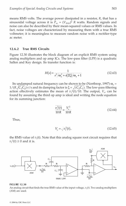
Examples of Special Analog Circuits and Systems 503
means RMS volts. The average power dissipated in a resistor, R, that has asinusoidal voltage across it is Pav = (VRMS)2 R watts. Random signals andnoise can also be described by their mean-squared values or RMS values. Infact, noise voltages are characterized by measuring them with a true RMSvoltmeter; it is meaningless to measure random noise with a rectifier-typeac meter.
12.6.2 True RMS Circuits
Figure 12.30 illustrates the block diagram of an explicit RMS system usinganalog multipliers and op amp ICs. The low-pass filter (LPF) is a quadraticSallen and Key design. Its transfer function is:
(12.63)
Its undamped natural frequency can be shown to be (Northrop, 1997) wn =1/(R ) r/s and its damping factor is x = . The low-pass filteringaction effectively estimates the mean of v1
2(t)/10. The output, Vo, can befound by assuming the third op amp is ideal and writing the node equationfor its summing junction:
(12.64)
Thus,
(12.65)
the RMS value of v1(t). Note that this analog square root circuit requires thatv1
2(t) ≥ 0 and it is.
FIGURE 12.30An analog circuit that finds the true RMS value of the input voltage, v1(t). Two analog multipliers(AM) are used.
H ss sn n
( ) =+ ( ) +
12 12 2w x w
C1C2 C2C1( )
v tR
VR
o12 2
10 10( ) =
V v to = ( )12 ,
R
____v1
2(t)
AM
Vo
Vo2
10
v12(t)
S&K LPF
C1
C2
R R
10
10
Rv1(t)
AM
© 2004 by CRC Press LLC
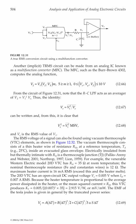
504 Analysis and Application of Analog Electronic Circuits
Another (implicit) TRMS circuit can be made from an analog IC knownas a multifunction converter (MFC). The MFC, such as the Burr–Brown 4302,computes the analog function,
(12.66)
From the circuit of Figure 12.31, note that the R–C LPF acts as an averagerof V2 = V1
2 Vo. Thus, the identity:
(12.67)
can be written and, from this, it is clear that
(12.68)
and Vo is the RMS value of V1.The RMS voltage of a signal can also be found using vacuum thermocouple
sists of a thin heater wire of resistance RHo at a reference temperature, TA
(e.g., 25ºC), inside an evacuated glass envelope. Electrically insulated frombut thermally intimate with RH is a thermocouple junction (TJ) (Pallàs–Arenyand Webster, 2001; Northrop, 1997; Lion, 1959). For example, the venerableWestern Electric model 20D VTC has RH = 35 W at room temperature; thenominal thermocouple resistance (Fe and constantan wires) is 12 W. Themaximum heater current is 16 mA RMS (exceed this and the heater melts).The 20D VTC has an open-circuit DC output voltage Vo = 0.005 V when IH =0.007 A RMS. Because the heater temperature is proportional to the averagepower dissipated in the heater, or the mean squared current ¥ RH, this VTCproduces KT = 0.005/[(0.007)2 ¥ 35] = 2.915 V/W, or mV/mW. The EMF ofthe tesla joules is given in general by the truncated power series:
(12.69)
FIGURE 12.31A true RMS conversion circuit using a multifunction converter.
VY(VZ /Vx )mV1
VX
MFCVY
Vo
VZ C
R Vo
m = 1 V12 /Vo (×1 Buffer)
V V V V m m V V V VY Z X x y Z2 5 1 0 10= ( ) ≥ ≥ £ ( ) £, , , ,
V V Vo o= 12
V Vo2
12= MSV,
V A T B T C T S TJ = ( ) + ( ) + ( ) @D D D D2 32 3
© 2004 by CRC Press LLC
(VTC) elements, as shown in Figure 12.32. The vacuum thermocouple con-
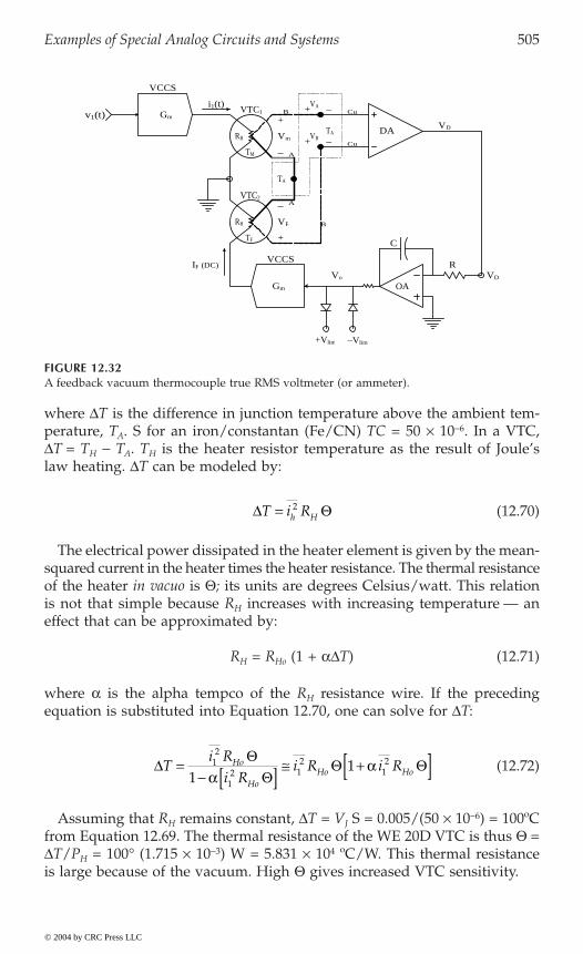
Examples of Special Analog Circuits and Systems 505
where DT is the difference in junction temperature above the ambient tem-perature, TA. S for an iron/constantan (Fe/CN) TC = 50 ¥ 10-6. In a VTC,DT = TH - TA. TH is the heater resistor temperature as the result of Joule’slaw heating. DT can be modeled by:
(12.70)
The electrical power dissipated in the heater element is given by the mean-squared current in the heater times the heater resistance. The thermal resistanceof the heater in vacuo is Q; its units are degrees Celsius/watt. This relationis not that simple because RH increases with increasing temperature — aneffect that can be approximated by:
RH = RHo (1 + aDT) (12.71)
where a is the alpha tempco of the RH resistance wire. If the precedingequation is substituted into Equation 12.70, one can solve for DT:
(12.72)
Assuming that RH remains constant, DT = VJ S = 0.005/(50 ¥ 10-6) = 100ºCfrom Equation 12.69. The thermal resistance of the WE 20D VTC is thus Q =DT/PH = 100∞ (1.715 ¥ 10-3) W = 5.831 ¥ 104 ºC/W. This thermal resistanceis large because of the vacuum. High Q gives increased VTC sensitivity.
FIGURE 12.32A feedback vacuum thermocouple true RMS voltmeter (or ammeter).
Gm
VB
TA
RH Vm
VCCS
+Vlim −Vlim
+TF C
VDVo
TAVD
−+Gm +
i1(t) VTC1 Cu
−+ Cu
DA
VA
OA
VCCSRIF (DC)
v1(t)
VTC2
B
TM A−
− A
RH VF B
D QT i Rh H= 2
DQ
QQ QT
i Ri R
i R i RHo
HoHo Ho=
- [ ] @ +[ ]12
12 1
212
11
aa
© 2004 by CRC Press LLC

506 Analysis and Application of Analog Electronic Circuits
12.72 into Equation 12.69. Examination of the TRMS TC feedback voltmeterF
Vm and it can be shown from the thermoelectric laws that VA – VB = 0, soVD = 0. VF and Vm are given approximately by:
(12.73)
From this equation, it can be written that
(12.74)
i.e., Vo equals the RMS value of v1(t).Note that this system is an even-error system. That is, the voltage VF is
independent of the sign of Vo because the same heating occurs regardless ofthe sign of IF in RH. Not shown but necessary to the operation of this systemis a means of initially setting Vo Æ 0 just before the measurement is made.Then Vo and IF increase until VD Æ 0 and Vm = VF.
Still another class of true RMS to DC converters is found in the AnalogDevices’ AD536A/636 and AD637 ICs. Figure 12.33 illustrates the blockdiagram of the AD637 TRMS converter IC. The front end of this systemmakes use of the identity:
(12.75)
Squaring is done by taking the logarithm of v1 and doubling it. Divisionby Vo is accomplished by subtracting the log of the dc output voltage, Vo,from 2 log(v1), giving V2, which is antilogged to recover v1
2(t) Vo. v12(t) Vo is
low-pass filtered to produce the implicitly derived DC RMS output voltage1
FIGURE 12.33Simplified block diagram of Analog Devices’ AD637 true analog RMS conversion IC.
−
(log)
(Divider = log subtractor)
log(Vo)
(DC)
Vo
*= 2 log[v1(t)]
V2 = 2 log[v1(t)] − log(Vo)
v1(t) log[v1(t)2] v12(t)/ Vo
10kV2
(Absval) (LPF)(log squarer) (antilog)____
Vo = v12(t)/ Vo
V2
____Vo = √ v1(t)
2
v1(t)+
V A I R A V G R V A v t G RF F Ho o m Ho m m Ho@ [ ] = ( )[ ] = @ ( )( )ÈÎÍ
ùûú
2 2
1
2Q Q Q
V DC v to ( ) = ( )[ ]12
v v12
1
20= ≥
© 2004 by CRC Press LLC
In the feedback TRMS meter, the TC EMF is found by substituting Equation
of Figure 12.32 shows that it is a self-nulling system. At equilibrium, V =
from v (t). Figure 12.34 illustrates the organization of the TRMS subsystems
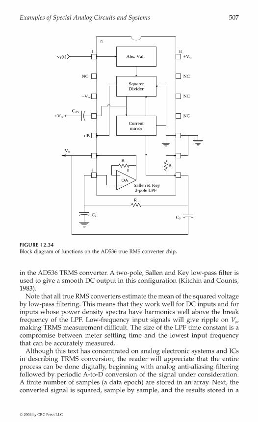
Examples of Special Analog Circuits and Systems 507
in the AD536 TRMS converter. A two-pole, Sallen and Key low-pass filter isused to give a smooth DC output in this configuration (Kitchin and Counts,1983).
Note that all true RMS converters estimate the mean of the squared voltageby low-pass filtering. This means that they work well for DC inputs and forinputs whose power density spectra have harmonics well above the breakfrequency of the LPF. Low-frequency input signals will give ripple on Vo,making TRMS measurement difficult. The size of the LPF time constant is acompromise between meter settling time and the lowest input frequencythat can be accurately measured.
Although this text has concentrated on analog electronic systems and ICsin describing TRMS conversion, the reader will appreciate that the entireprocess can be done digitally, beginning with analog anti-aliasing filteringfollowed by periodic A-to-D conversion of the signal under consideration.A finite number of samples (a data epoch) are stored in an array. Next, theconverted signal is squared, sample by sample, and the results stored in a
FIGURE 12.34Block diagram of functions on the AD536 true RMS converter chip.
SquarerDivider
Currentmirror
Sallen & Key2-pole LPF
OA
Vo
Abs. Val.v1(t) +Vcc
−Vcc
NC NC
NC
NC
dB
+Vcc
CAV
RR
R
C2 C3
1
7 8
14
© 2004 by CRC Press LLC

508 Analysis and Application of Analog Electronic Circuits
second array. The squared samples are then numerically low-pass filtered toestimate their mean. The numerical square root of the mean squared valueis taken and stored for the kth epoch. The process is repeated until M epochshave been processed; then the average of M estimates of the RMS signal isfinally calculated. The only components required are the anti-aliasing LPF,an ADC, some interface chips, and, of course, a PC.
12.7 IC Thermometers
12.7.1 Introduction
Temperature measurement is very important in medicine and biology. Manymeans have been devised to measure temperature, based on the fact thatmany physical phenomena vary with temperature, including, but not limitedto: physical volume expansion (mercury and alcohol thermometers); resistance;EMF generated by the Seebeck (thermoelectric) effect; change in pemittivityof materials; change in reverse current through a pn junction; etc.
Many electronic means have been devised to circumvent use of the slow(and toxic) mercury thermometer. The fact that the resistance of metalsincreases with temperature has been the basis of one important class ofelectronic thermometer. The platinum resistance temperature detector (RTD)is widely used in scientific applications (Northrop, 1997). Its resistance ismodeled by the truncated power series:
(12.76)
where Ro is the Pt RTD’s resistance at 0∞C and T is the RTD’s temperaturein degrees Celsius.
RTD resistance changes are sensed by using a Wheatstone bridge andsuitable electronic amplification. Often a look-up table is used to correct forslight nonlinearity in the platinum RTD’s resistance vs. T characteristic. Thelook-up table can be in the form of an ROM in which correction values arestored. Other metals (Ni, W, Cu, Si) can be used for RTD design, but Pt isthe one most widely encountered because its R(T) is fairly linear comparedto other metals and it can be used at elevated (industrial) temperatures.
Thermistors are also used with Wheatstone bridges to sense temperature.Thermistors are amorphous semiconductor resistors; they are very nonlinear,but have much greater thermal sensitivity compared to metal RTDs. Theresistance of a negative temperature coefficient (NTC) thermistor is modeledby the relation (Northrop, 1997):
(12.77)
R T R T To( ) = + ¥ - ¥[ ]- -1 3 908 10 5 8 103 7 2. .
R T R T To o( ) = -( )[ ]exp b 1 1
© 2004 by CRC Press LLC
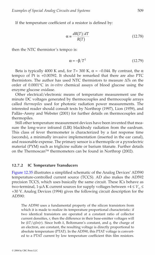
Examples of Special Analog Circuits and Systems 509
If the temperature coefficient of a resistor is defined by:
(12.78)
then the NTC thermistor’s tempco is:
(12.79)
Beta is typically 4000 K and, for T= 300 K, a = -0.044. By contrast, the atempco of Pt is +0.00392. It should be remarked that there are also PTCthermistors. The author has used NTC thermistors to measure DTs on theorder of 0.0001∞C in in-vitro chemical assays of blood glucose using theenzyme glucose oxidase.
Other electrical/electronic means of temperature measurement use theminute DC voltages generated by thermocouples and thermocouple arrayscalled thermopiles used for photonic radiation power measurements. Theinterested reader should consult texts by Northrop (1997), Lion (1959), andPallàs–Areny and Webster (2001) for further details on thermocouples andthermopiles.
Still other temperature measurement devices have been invented that mea-sure the long-wave infrared (LIR) blackbody radiation from the eardrum.This class of fever thermometer is characterized by a fast response time(seconds), a minimally invasive implementation (inserted in the ear canal),and reasonable expense. The primary sensor is a thermopile or a pyroelectricmaterial (PYM) such as triglicine sulfate or barium titanate. Further detailson the Thermoscan thermometers can be found in Northrop (2002).
12.7.2 IC Temperature Transducers
temperature-controlled current source (TCCS). AD also makes the AD592precision TCCS, which uses basically the same circuit. These ICs behave astwo-terminal, 1-mA K current sources for supply voltages between +4 £ Vcc £+30 V. Analog Devices (1994) gives the following circuit description for theAD590:
The AD590 uses a fundamental property of the silicon transistors fromwhich it is made to realize its temperature proportional characteristic: iftwo identical transistors are operated at a constant ratio of collectorcurrent densities, r, then the difference in their base-emitter voltages willbe (kT/q)ln(r). Since both k, Boltzmann’s constant, and q, the charge ofan electron, are constant, the resulting voltage is directly proportional toabsolute temperature (PTAT). In the AD590, this PTAT voltage is convert-ed to a PTAT current by low temperature coefficient thin film resistors.
a ∫ ( )( )
dR T dTR T
a b= - T2
© 2004 by CRC Press LLC
Figure 12.35 illustrates a simplified schematic of the Analog Devices’ AD590
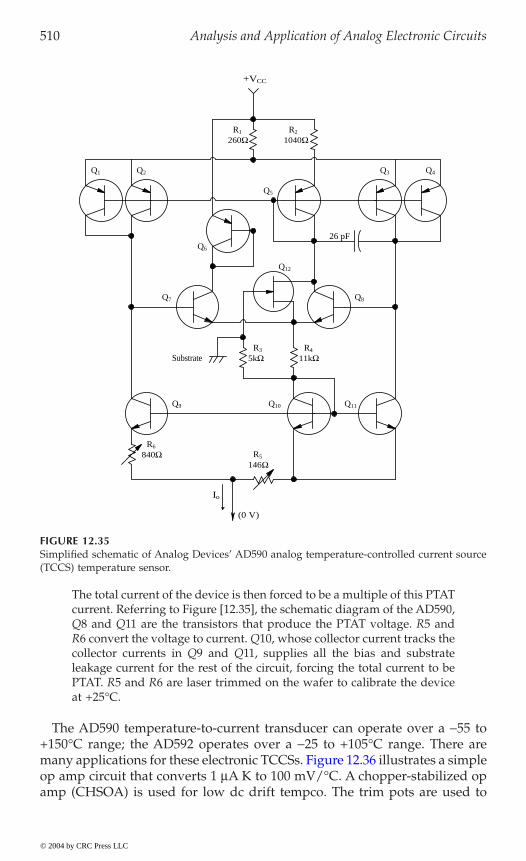
510 Analysis and Application of Analog Electronic Circuits
The total current of the device is then forced to be a multiple of this PTATcurrent. Referring to Figure [12.35], the schematic diagram of the AD590,Q8 and Q11 are the transistors that produce the PTAT voltage. R5 andR6 convert the voltage to current. Q10, whose collector current tracks thecollector currents in Q9 and Q11, supplies all the bias and substrateleakage current for the rest of the circuit, forcing the total current to bePTAT. R5 and R6 are laser trimmed on the wafer to calibrate the deviceat +25∞C.
The AD590 temperature-to-current transducer can operate over a -55 to+150∞C range; the AD592 operates over a -25 to +105∞C range. There are
op amp circuit that converts 1 mA K to 100 mV/∞C. A chopper-stabilized opamp (CHSOA) is used for low dc drift tempco. The trim pots are used to
FIGURE 12.35Simplified schematic of Analog Devices’ AD590 analog temperature-controlled current source(TCCS) temperature sensor.
+VCC
260Ω 1040Ω
26 pF
840Ω146Ω
Substrate 5kΩ 11kΩ
R1 R2
Q8
Q9 Q10 Q11
R6
R5
Q12
Q7
R4R3
Q6
Q5
Q1 Q2 Q3 Q4
Io
(0 V)
© 2004 by CRC Press LLC
many applications for these electronic TCCSs. Figure 12.36 illustrates a simple
Examples of Special Analog Circuits and Systems 511
calibrate the amplifier exactly so that it has zero gain and offset error at thedesign temperature, e.g., 37∞C.
Note that National Semiconductor also makes IC temperature sensors. TheNational LM135 series of sensors behave as temperature-controlled voltagedrops (much like a zener diode). They give 10 mV/K drop with approxi-mately 1-W dynamic resistance for DC currents ranging from 400 mA to 5 mA.They cover a wide, -55 to +150∞C range. The National LM35 precisionCelsius temperature sensor is a three-terminal device that outputs an EMFof 10 mV/∞C over a -55 to +150∞C range, given a supply voltage from 4 to30 VDC.
12.8 Instrumentation Systems
12.8.1 Introduction
The previous sections of this chapter have described and analyzed the char-acteristics of selected ICs useful in designing biomedical instrumentationsystems. This section focuses on examples of biomedical instrumentationsystems taken from the research of the author and some of his graduatestudents. In each system, op amps are used extensively for various linearand nonlinear subsystems.
12.8.2 A Self-Nulling Microdegree Polarimeter
A polarimeter is an instrument used to measure the angle of rotation oflinearly polarized light when it is passed through an optically active material.There are many types of polarimeters as well as a number of optically active
FIGURE 12.36A simple op amp current-to-voltage converter that converts the current output of an AD592temperature sensor to 100 mV/∞C.
1 µA/oK
+ 2.5 V8.66 kΩ
97.6 kΩ 5 kΩ
AD592T
−15 V
(0)Vo = 100 mV/oC
CHSOA1 kΩ +
−
© 2004 by CRC Press LLC
512 Analysis and Application of Analog Electronic Circuits
substances found in living systems; probably the most important is dissolvedD-glucose. Clear biological liquids such as urine, blood plasma, and theaqueous humor of the eyes contain dissolved D-glucose with a molar con-centration in proportion to the blood glucose concentration (Northrop, 2002).Using polarimetry, D-glucose concentration can be measured by the simplerelation:
(12.80)
where f is the measured optical rotation of linearly polarized light (LPL) ofwavelength l passed through a sample chamber of length L containing theoptically active analyte at concentration C and temperature T.
The constant [a]lT is called the specific optical rotation of the analyte; its
units are generally in degrees per (optical path length unit ¥ concentrationunit). [a]l
T for D-glucose in 25∞C water and at 512 nm is 0.0695 milli-degrees/(cm ¥ g/dl). Thus, the optical rotation of a 1-g/l solution of D-glucosein a 10-cm cell is 69.5 millidegrees. Note that [a]l
T can have either sign,depending on the analyte; if N optically active substances are present in thesample chamber, the net optical rotation is given by superposition:
(12.81)
To describe how a polarimeter works, one must first describe what is meantby linearly polarized light. When light from an incoherent source such as atungsten lamp is treated as an electromagnetic wave phenomenon (ratherthan photons), the propagating radiation is composed of a broad spectrumof wavelengths and polarization states. To facilitate the description of LPL,
light in the medium in which it is traveling. This velocity in the z-direction
of the propagation medium (generally >1.0). A beam of monochromatic lightcan have a variety of polarization states, including random (unpolarized),
illustrates an LPL ray in which the E-vector propagates entirely in the x–zplane, and its orthogonal By–vector lies in the y–z plane; E and B are in-phase and both vectors are functions of time and distance.
For the Ex(t, z) vector:
(12.82)
Note that the E-vector need not lie in the x–z plane; its plane of propagationcan be tilted some angle q with respect to the x-axis and still propagate in
f a l= [ ]T C L degrees
f a l= [ ]=
ÂL CTk
k
Nk
1
E Ex oxt zc
t z, cos( ) = -ÈÎÍ
ùûú
2 2pl
pl
© 2004 by CRC Press LLC
is v = c/n m/s; c is the velocity of light in vacuo and n is the refractive index
examine a monochromatic ray propagating in the z-direction at the speed of
circular (CW or CCW), elliptical, and linear (Balanis, 1989). Figure 12.37
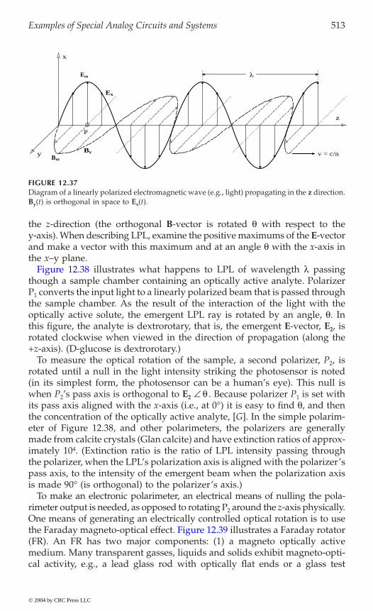
Examples of Special Analog Circuits and Systems 513
the z-direction (the orthogonal B-vector is rotated q with respect to they-axis). When describing LPL, examine the positive maximums of the E-vectorand make a vector with this maximum and at an angle q with the x-axis inthe x–y plane.
though a sample chamber containing an optically active analyte. PolarizerP1 converts the input light to a linearly polarized beam that is passed throughthe sample chamber. As the result of the interaction of the light with theoptically active solute, the emergent LPL ray is rotated by an angle, q. Inthis figure, the analyte is dextrorotary, that is, the emergent E-vector, E2, isrotated clockwise when viewed in the direction of propagation (along the+z-axis). (D-glucose is dextrorotary.)
To measure the optical rotation of the sample, a second polarizer, P2, isrotated until a null in the light intensity striking the photosensor is noted(in its simplest form, the photosensor can be a human’s eye). This null iswhen P2’s pass axis is orthogonal to E2 q . Because polarizer P1 is set withits pass axis aligned with the x-axis (i.e., at 0∞) it is easy to find q, and thenthe concentration of the optically active analyte, [G]. In the simple polarim-eter of Figure 12.38, and other polarimeters, the polarizers are generallymade from calcite crystals (Glan calcite) and have extinction ratios of approx-imately 104. (Extinction ratio is the ratio of LPL intensity passing throughthe polarizer, when the LPL’s polarization axis is aligned with the polarizer’spass axis, to the intensity of the emergent beam when the polarization axisis made 90∞ (is orthogonal) to the polarizer’s axis.)
To make an electronic polarimeter, an electrical means of nulling the pola-rimeter output is needed, as opposed to rotating P2 around the z-axis physically.One means of generating an electrically controlled optical rotation is to use
(FR). An FR has two major components: (1) a magneto optically activemedium. Many transparent gasses, liquids and solids exhibit magneto-opti-cal activity, e.g., a lead glass rod with optically flat ends or a glass test
FIGURE 12.37Diagram of a linearly polarized electromagnetic wave (e.g., light) propagating in the z direction.By(t) is orthogonal in space to Ex(t).
x
y
z
P
l
v = c/n
Eox
Ex
By
Boy
© 2004 by CRC Press LLC
Figure 12.38 illustrates what happens to LPL of wavelength l passing
the Faraday magneto-optical effect. Figure 12.39 illustrates a Faraday rotator
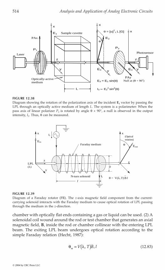
514 Analysis and Application of Analog Electronic Circuits
chamber with optically flat ends containing a gas or liquid can be used. (2) Asolenoidal coil wound around the rod or test chamber that generates an axialmagnetic field, B, inside the rod or chamber collinear with the entering LPLbeam. The exiting LPL beam undergoes optical rotation according to thesimple Faraday relation (Hecht, 1987):
(12.83)
FIGURE 12.38Diagram showing the rotation of the polarization axis of the incident E1 vector by passing theLPL through an optically active medium of length L. The system is a polarimeter: When thepass axis of linear polarizer P2 is rotated by angle q + 90∞, a null is observed in the outputintensity, I3. Thus, q can be measured.
FIGURE 12.39Diagram of a Faraday rotator (FR). The z-axis magnetic field component from the current-carrying solenoid interacts with the Faraday medium to cause optical rotation of LPL passingthrough the medium in the z-direction.
E2
E3
P2
y y y
x
x
z z z
P1
L
q
E3
E1
Laser
Sample cuvette
Photosensor
Optically-activemedium E3 = E2 sin(q) Null at (q + 90o)
x
q = [a]Tl L [G]
I3 µ E22 sin2(q)
PAx
PAy
x
zz
y y
EoutqFaraday medium
LPL
x
Ein
D
(Opticalrotation)
N-turn solenoid_
q = V(l, T) B ll
(l)
Ic
Ic
q lm zV T B l= ( ),
© 2004 by CRC Press LLC
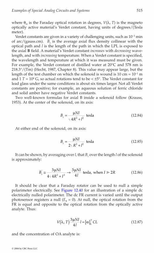
Examples of Special Analog Circuits and Systems 515
where qm is the Faraday optical rotation in degrees, V(l, T) is the magnetooptically active material’s Verdet constant, having units of degrees/(Teslameter).
Verdet constants are given in a variety of challenging units, such as 10-3 minof arc/(gauss.cm). `Bz is the average axial flux density collinear with theoptical path and l is the length of the path in which the LPL is exposed tothe axial B field. A material’s Verdet constant increases with decreasing wave-length, and with increasing temperature. When a Verdet constant is specified,the wavelength and temperature at which it was measured must be given.For example, the Verdet constant of distilled water at 20∞C and 578 nm is218.3∞/(Tm) (Hecht, 1987, Chapter 8). This value may appear large, but thelength of the test chamber on which the solenoid is wound is 10 cm = 10-1 mand 1 T = 104 G, so actual rotations tend to be < ±5∞. The Verdet constant forlead glass under the same conditions is about six times larger. Not all Verdetconstants are positive; for example, an aqueous solution of ferric chlorideand solid amber have negative Verdet constants.
Two well-known formulas for axial B inside a solenoid follow (Krauss,1953). At the center of the solenoid, on its axis:
(12.84)
At either end of the solenoid, on its axis:
(12.85)
It can be shown, by averaging over l, that Bz over the length l of the solenoidis approximately:
(12.86)
It should be clear that a Faraday rotator can be used to null a simple
electrically nulled polarimeter. The dc FR current is varied until the outputphotosensor registers a null (E4 = 0). At null, the optical rotation from theFR is equal and opposite to the optical rotation from the optically activeanalyte. Thus:
(12.87)
and the concentration of OA analyte is:
BNI
R lz =
+m
4 2 2 tesla
BNI
R lz =
+m
2 2 2 tesla
BNI
R I
NIl
I Rz @+
Æ3
4 4
34
22 2
m m tesla, when
V TNIl
l CLTl m a l,( ) = [ ]34
© 2004 by CRC Press LLC
polarimeter electrically. See Figure 12.40 for an illustration of a simple dc
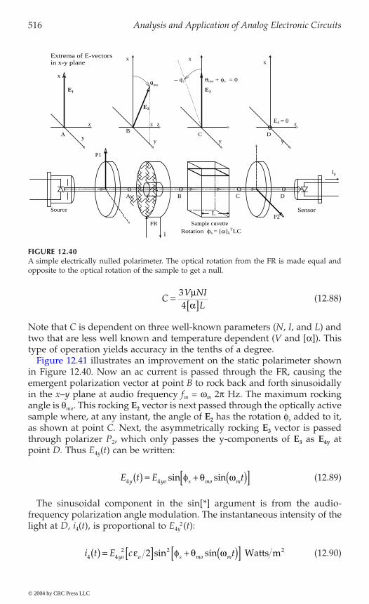
516 Analysis and Application of Analog Electronic Circuits
(12.88)
Note that C is dependent on three well-known parameters (N, I, and L) andtwo that are less well known and temperature dependent (V and [a]). Thistype of operation yields accuracy in the tenths of a degree.
in Figure 12.40. Now an ac current is passed through the FR, causing theemergent polarization vector at point B to rock back and forth sinusoidallyin the x–y plane at audio frequency fm = wm 2p Hz. The maximum rockingangle is qmo. This rocking E2 vector is next passed through the optically activesample where, at any instant, the angle of E2 has the rotation fs added to it,as shown at point C. Next, the asymmetrically rocking E3 vector is passedthrough polarizer P2, which only passes the y-components of E3 as E4y atpoint D. Thus E4y(t) can be written:
(12.89)
The sinusoidal component in the sin[*] argument is from the audio-frequency polarization angle modulation. The instantaneous intensity of thelight at D, i4(t), is proportional to E4y
2(t):
(12.90)
FIGURE 12.40A simple electrically nulled polarimeter. The optical rotation from the FR is made equal andopposite to the optical rotation of the sample to get a null.
x
A B C D
SensorP2
x x
z
FR Sample cuvetteRotation φs = [α]λ
TLC
Ip
i
Source
E1
Extrema of E-vectors
L
E3
in x-y plane
zz z
P1
DCy
yB
Ay y
θmo
x− φs θmo + φs = 0
E2
E4 = 0
CV NI
L= [ ]
34
ma
E t E ty yo s mo m4 4( ) = + ( )[ ]sin sinf q w
i t E c tyo o s mo m4 42 2 22( ) = [ ] + ( )[ ]e f q wsin sin Watts m
© 2004 by CRC Press LLC
Figure 12.41 illustrates an improvement on the static polarimeter shown
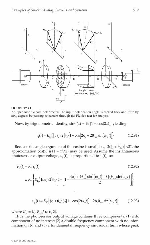
Examples of Special Analog Circuits and Systems 517
Now, by trigonometric identity, sin2 (x) = ½ [1 - cos(2x)], yielding:
(12.91)
Because the angle argument of the cosine is small, i.e., 2(fs + qmo) <3∞, theapproximation cos(x) @ (1 - x2/2) may be used. Assume the instantaneousphotosensor output voltage, vp(t), is proportional to i4(t), so:
Ø
(12.93)
where KV = KP E4yo2 (c eo 2).
Thus the photosensor output voltage contains three components: (1) a dccomponent of no interest; (2) a double-frequency component with no infor-mation on fs; and (3) a fundamental frequency sinusoidal term whose peak
FIGURE 12.41An open-loop Gilham polarimeter. The input polarization angle is rocked back and forth by±qmo degrees by passing ac current through the FR. See text for analysis.
x
E3E2
A B C D
D
E4
E2
θmo + φs
E3
φs − θmo
θmo
−θmo
φs
Sensor
Cy
y
zzB
P1
P2
x x
y
z z
Sample cuvetteRotation φs = [α]λ
TLC
Ip
Source
E1
x
A
L
FRi
i t E c tyo o s mo m4 42 1
22 1 2 2( ) = [ ] - + ( )[ ] e f q wcos sin
v t K i t
K E ct t
p P
P yo os mo m s mo m
( ) = ( )
@ ( ) - -+ ( ) + ( )È
ÎÍÍ
ù
ûúú
ÏÌÔ
ÓÔ
ÏÌÔ
ÓÔ
¸ýÔ
þÔ
4
42 1
2
2 2 2
2 1 14 4 8
2e
f q w f q wsin sin
(12.92)
v t K t tp V s mo m s mo m( ) = + - ( )( ) + ( )[ ]f q w f q w2 2 12 1 2 2cos sin
© 2004 by CRC Press LLC
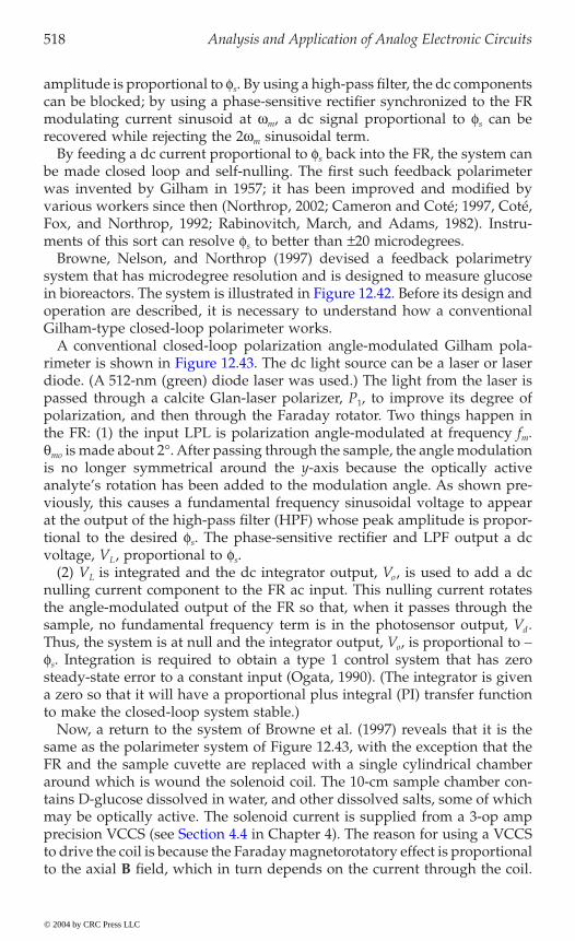
518 Analysis and Application of Analog Electronic Circuits
amplitude is proportional to fs. By using a high-pass filter, the dc componentscan be blocked; by using a phase-sensitive rectifier synchronized to the FRmodulating current sinusoid at wm, a dc signal proportional to fs can berecovered while rejecting the 2wm sinusoidal term.
By feeding a dc current proportional to fs back into the FR, the system canbe made closed loop and self-nulling. The first such feedback polarimeterwas invented by Gilham in 1957; it has been improved and modified byvarious workers since then (Northrop, 2002; Cameron and Coté; 1997, Coté,Fox, and Northrop, 1992; Rabinovitch, March, and Adams, 1982). Instru-ments of this sort can resolve fs to better than ±20 microdegrees.
Browne, Nelson, and Northrop (1997) devised a feedback polarimetrysystem that has microdegree resolution and is designed to measure glucose
operation are described, it is necessary to understand how a conventionalGilham-type closed-loop polarimeter works.
A conventional closed-loop polarization angle-modulated Gilham pola-
diode. (A 512-nm (green) diode laser was used.) The light from the laser ispassed through a calcite Glan-laser polarizer, P1, to improve its degree ofpolarization, and then through the Faraday rotator. Two things happen inthe FR: (1) the input LPL is polarization angle-modulated at frequency fm.qmo is made about 2∞. After passing through the sample, the angle modulationis no longer symmetrical around the y-axis because the optically activeanalyte’s rotation has been added to the modulation angle. As shown pre-viously, this causes a fundamental frequency sinusoidal voltage to appearat the output of the high-pass filter (HPF) whose peak amplitude is propor-tional to the desired fs. The phase-sensitive rectifier and LPF output a dcvoltage, VL, proportional to fs.
(2) VL is integrated and the dc integrator output, Vo, is used to add a dcnulling current component to the FR ac input. This nulling current rotatesthe angle-modulated output of the FR so that, when it passes through thesample, no fundamental frequency term is in the photosensor output, Vd.Thus, the system is at null and the integrator output, Vo, is proportional to -fs. Integration is required to obtain a type 1 control system that has zerosteady-state error to a constant input (Ogata, 1990). (The integrator is givena zero so that it will have a proportional plus integral (PI) transfer functionto make the closed-loop system stable.)
Now, a return to the system of Browne et al. (1997) reveals that it is thesame as the polarimeter system of Figure 12.43, with the exception that theFR and the sample cuvette are replaced with a single cylindrical chamberaround which is wound the solenoid coil. The 10-cm sample chamber con-tains D-glucose dissolved in water, and other dissolved salts, some of whichmay be optically active. The solenoid current is supplied from a 3-op amp
to drive the coil is because the Faraday magnetorotatory effect is proportionalto the axial B field, which in turn depends on the current through the coil.
© 2004 by CRC Press LLC
in bioreactors. The system is illustrated in Figure 12.42. Before its design and
rimeter is shown in Figure 12.43. The dc light source can be a laser or laser
precision VCCS (see Section 4.4 in Chapter 4). The reason for using a VCCS
Examples of Special Analog Circuits and Systems 519
Because the coil is lossy, it gradually heats from the power dissipated by theac modulation excitation and the dc nulling current. As the coil wire tem-perature increases, its resistance goes up. Thus, if a voltage source (op amp)were used to drive the coil, B would be a function of temperature as wellas the input voltage, Vc. The B temperature dependence is eliminated byusing the VCCS.
FIGURE 12.42A system devised by the author to measure the concentration of dissolved glucose. It is a self-nulling Gilham-type polarimeter in which the external FR has been replaced by the Faradaymagneto-optical effect of the water solvent in the test chamber. Glucose is the optically activemedium (analyte) dissolved in the water.
VD
RD
L’
Solid-stateLaser
P2
HPF
Photodiode
N turns
10 cm samplechamber
R
Vm @ ωm
R
(dc)
VLLPFPSR
Phaseshifter
R3
C
−+ R4
Integrator
Sync.
Analyte +water
Oscillator
R
R
(coil length)Vo
VCCS
P1
−Vc
POAR2
ICRF
R1
Vc
© 2004 by CRC Press LLC

520 Analysis and Application of Analog Electronic Circuits
The FR can be eliminated because the water solvent in the chamber has aVerdet constant and, when subject to ac and dc magnetic fields, causes opticalrotation of the transmitted LPL. The glucose solute is optically active, so, inthe same path length, Faraday rotation occurs because of the action of B onthe water and optical rotation occurs because of the dissolved D-glucose.
It is possible to summarize the operation of this interesting system by ablock diagram, shown in Figure 12.44. The input to the measurement system
FIGURE 12.43A conventional self-nulling Gilham-type polarimeter. A VCCS is used to drive the external FR’scoil, which carries the ac modulation signal and the dc nulling current. A PSR/LPF is used tosense null.
FIGURE 12.44
P1
RF
ic
xx
yy
P2
PA
PA
POA
Light source
Phaseshifter
Osc.
Vm
Vo
VCCS
ωn
PSRLPF PRAHPF
(dc)
L
Vd
R
R
R
Integrator
Photosensor
FR Sample
VL (dc)
RVc
Rm
(τLs + 1)
VL
−Ki(τi s + 1)s
Vo’
Vo
Current source,
PSR LPF
Integrator
coil & FR LPF
φF
Implicit anglesubtraction
(τos + 1)1
φs KLφe
I4 θmo KP
−KFR
−
© 2004 by CRC Press LLC
A block diagram describing the dynamics of the novel polarimeter of Figure 12.42.
Examples of Special Analog Circuits and Systems 521
is the physical angle of rotation of the polarization vector, fs, caused bypassing the LPL through the optically active analyte. The negative feedbackof the system output voltage, Vo, leads to a Faraday counter-rotation of theLPL, fF, forming a net (error) rotation, fe. The dc counter-rotation, fF, issimply:
(12.94)
Clearly, KFR = V (3/4) m N R/(R1RF) degrees/volt. The closed-loop responseof the system is found from the block diagram:
(12.95)
It is of interest to consider the dc or steady-state response of this closed-loop polarimeter to a constant fs. This can be shown to be:
(12.96)
Equation 12.96 is a rather serendipitous result, revealing that the system’scalibration depends only on KFR, which depends on the transconductance ofthe VCCS, the dimensions and number of turns of the coil, the Verdet con-stant, and the permeability (m) of water. The dc gain is independent of thelight intensity (I4), the depth of polarization angle modulation (qmo), thefrequency of modulation (wm), and the system’s gain parameters (KP, KL, andKi) and time constants (tL and ti ).
The prototype system built and tested by Browne et al. (1997) was evalu-ated for D-glucose concentrations (x) from 60 to 140 mg/dl. By least mean-square error curve fitting, the output voltage (y) was found to follow thelinear model,
y = 0.0544 x + 0.0846 (12.97)
with R2 = 0.9986. System resolution was 10.1 mo/mV out, at 27∞C with a 10-cmcell, and the glucose sensitivity was 55.4 mV/mg%. Noise in Vo was reduced
f m mF co
FFR oVBL V
NL
L I V NV RR R
K V= ¢ = ( )¢
¢ = ( )[ ] -È
ÎÍ
ù
ûú = -3 4 3 4
1
Vs
I K K K s
s s I K K K K I K K K Ko
s
mo P L i i
L i mo P L i FR mo P L i FRfq t
t t q q( ) =
- +( )+ +[ ] +
42
4 4
11
VK
o
s FRf= -1
© 2004 by CRC Press LLC
by low-pass filtering (not shown in Figure 12.42).
resistor) (see Section 2.6.4 in Chapter 2); the phase-sensitive rectifier (see
Note that, in this instrument, op amps were used exclusively for all active
Section 12.2.3 in Chapter 12); the low-pass filter (see Section 7.2 in Chapter 7);
components, including the photodiode current-to-voltage converter (trans-
the PI integrator (see Section 6.6 in Chapter 6); the oscillator (see Section 5.5in Chapter 5); and the VCCS (see Section 4.4 in Chapter 4).

522 Analysis and Application of Analog Electronic Circuits
12.8.3 A Laser Velocimeter and Rangefinder
Many conventional laser-based velocimeters are based on a time-of-flightrangefinder principle in which laser pulses are reflected from a reflective(cooperative) target back to the source position and the range is found fromthe simple relation:
L = c D t 2 meters (12.98)
If the target is moving toward or away from the laser/photosensor assem-bly, the relative velocity can be found by approximating v =
·L by numerically
differentiating the sequence of return times for sequential output pulses,Dt = Â Dtk. In 1992, Laser Atlanta made a vehicular velocimeter that usedthis principle.
The laser velocimeter and rangefinder (LAVERA) system described in thissection uses quite a different principle to provide simultaneous velocity andrange output. The LAVERA system was developed by Northrop (1997) andreduced to practice by a graduate student (Nelson, 1999) for his MS researchin biomedical engineering at the University of Connecticut. The motivationfor developing the system was to make a walking aid for the blind that couldbe incorporated into a cane.
The system uses sinusoidally amplitude-modulated CW light from an NIRlaser diode (LAD). The beam from the LAD is reflected from the target objectand then travels back to the receiver photosensor where its intensity isconverted to an ac signal whose phase lags that of the transmitted light. Thephase lag is easily seen to be:
(12.99)
where, as discussed previously, Dt is the time it takes a photon to make a roundtrip to the target; T is the period of the modulation; and c is the speed of light.
The system developed is a closed-loop system that tries to keep Df constantregardless of the target range, L. This means that, as L decreases, T mustdecrease and, conversely, as L increases, T must increase to maintain a
of the LAVERA system. Start the analysis by considering the voltage-to-period converter (VPC), which is an oscillator in which the output period isproportional to VP. Thus:
T = 1/f = KVPC VP + b seconds (12.100)
By way of contrast, the output from a conventional voltage-to-frequencyoscillator is described by:
f = KVCO VC + d Hz (12.101)
D Df p p= ( ) ( ) = ( ) ( )2 2 2t T L c T radians
© 2004 by CRC Press LLC
constant phase difference. Figure 12.45 illustrates the functional architecture

Examples of Special Analog Circuits and Systems 523
Next, consider the phase detector. This subsystem measures the phasedifference between the transmitted modulated signal intensity and thedelayed, reflected modulated signal intensity. An analog multiplier can beused directly to measure this phase difference; however, in this system, theanalog sine waves proportional to light intensity are passed through com-parators to convert them to TTL waves with a phase difference sensed by
FIGURE 12.45Block diagram of the LAVERA system developed by Nelson (1999). Sinusoidal modulation ofthe laser beam’s intensity was used because less bandwidth is required for signal conditioningthan for a pulsed system. The system simultaneously measures target range and velocity.
FIGURE 12.46The EOR phase detector used in the LAVERA system, and its transfer function.
VCCS
LAD
CMP05
CMP05
Referencebeam
Targetbeam
L
L
HSM
PD
FSM
−15 V
VPC
−15 V
PDAMP
AMP
EOR
dc offset& LPF
Vφ P
Q
Target
−Ki (τi s + 1)s
− VP
Vv VL
Vr
Integrator
Q
P
R R
R
__Vz
1.7 V
0
−1.7 V
π/2 3π/2 5π/2 7π/2π 2π 3π θ
f
−1.7 V 1Vz
LPF__Vz
© 2004 by CRC Press LLC
524 Analysis and Application of Analog Electronic Circuits
an exclusive or (EOR) gate phase detector (PD). The EOR PD is a quadraturedetector, i.e., its output duty cycle is 50% when one input lags (or leads) the
illustrates the EOR PD’s waveforms and transfer function. The op ampinverts the TTL output of the EOR gate and subtracts a dc level so that Vz
swings ±1.7 V.For a heuristic view of how the system works, the PD output can be written
as:
(12.102)
In the steady-state with fixed L, Vv = 0 in a type 1 feedback loop. For Vv =0, fss = p/2. However, it has already been established that the phase lag fora returning modulated light beam is:
(12.103)
If Equation 12.103 for f is solved for T and T is substituted into the VPCequation,
(12.104)
Ø
(12.105)
If Vr ∫ b/KVPC, the final expression for VLss is obtained:
(12.106)
The steady-state VL is indeed proportional to L. Going back to the VPCequation, one finds that, for a stationary target, the steady-state VPC outputfrequency is given by:
(12.107)
At L = 1m, fss = 37.5 MHz; when L = 30 m, fss = 1.25 MHz, etc.Now suppose the target is moving away from the transmitter/receiver at
a constant velocity, v =·L. Vv is no longer zero, but can be found from the
integrator relation:
(12.108)
V V Vz vf p f= = = -( ) +3 4 1 7. . volts
f p= ( ) ( ) ( )2 2 1L c T radians
T L c K V bss ss VPC Pss= ( ) ( ) ( ) = +2 2 1p f
8L c K V V bVPC Lss r= -[ ] +
V L c KLss VPC= ( )8
f T c Lss ss= = ( )1 8 Hz.
V V KL
K K cv L ii VPC
= - = -˙˙8
© 2004 by CRC Press LLC
other by odd multiples of p/2. Figure 12.46 (adapted from Northrop, 1990)
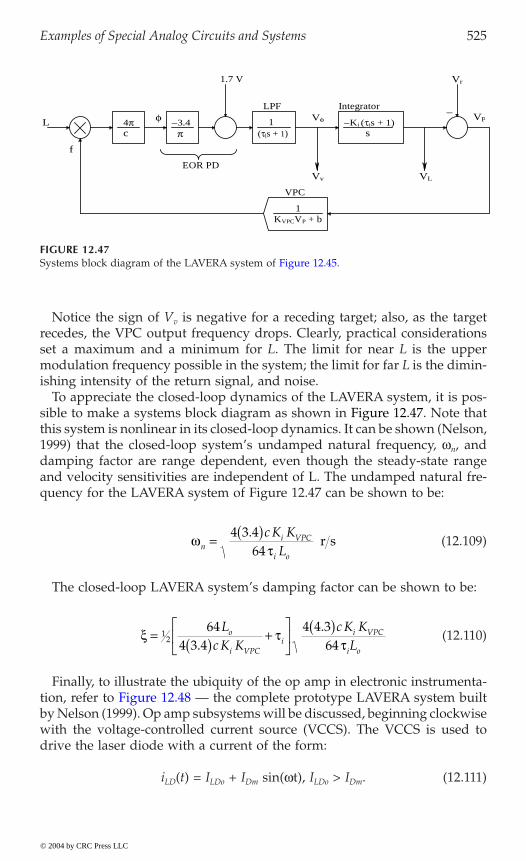
Examples of Special Analog Circuits and Systems 525
Notice the sign of Vv is negative for a receding target; also, as the targetrecedes, the VPC output frequency drops. Clearly, practical considerationsset a maximum and a minimum for L. The limit for near L is the uppermodulation frequency possible in the system; the limit for far L is the dimin-ishing intensity of the return signal, and noise.
To appreciate the closed-loop dynamics of the LAVERA system, it is pos-
this system is nonlinear in its closed-loop dynamics. It can be shown (Nelson,1999) that the closed-loop system’s undamped natural frequency, wn, anddamping factor are range dependent, even though the steady-state rangeand velocity sensitivities are independent of L. The undamped natural fre-quency for the LAVERA system of Figure 12.47 can be shown to be:
(12.109)
The closed-loop LAVERA system’s damping factor can be shown to be:
(12.110)
Finally, to illustrate the ubiquity of the op amp in electronic instrumenta-
by Nelson (1999). Op amp subsystems will be discussed, beginning clockwisewith the voltage-controlled current source (VCCS). The VCCS is used todrive the laser diode with a current of the form:
iLD(t) = ILDo + IDm sin(wt), ILDo > IDm. (12.111)
FIGURE 12.47
KVPCVP + b1
f
1.7 V
LPF Integrator
VPC
EOR PDVv
c π (τls + 1) sL
VL
Vr
φ4π −3.4 1 −Ki (τis + 1)
VPVφ−
wtn
i VPC
i o
c K KL
= ( )4 3 464
. r s
x tt
= ( ) +È
ÎÍ
ù
ûú
( )12
644 3 4
4 4 364
Lc K K
c K KL
o
i VPCi
i VPC
i o..
© 2004 by CRC Press LLC
Systems block diagram of the LAVERA system of Figure 12.45.
sible to make a systems block diagram as shown in Figure 12.47. Note that
tion, refer to Figure 12.48 — the complete prototype LAVERA system built
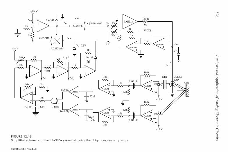
526A
nalysis and Application of A
nalog Electronic C
ircuitsFIGURE 12.48Simplified schematic of the LAVERA system showing the ubiquitous use of op amps.
1k
1k
1k
1k
CMP05
CMP05
MAX038
-5 V
100k
100k
2k
10k
10k
10k
10k
500
1k
CQL800LAD
3.3k
3.3k
0.047 mF
10k NDF
0.047 mFOBJ
90 pF
90 pFcable
74F864.7 mF
1k
110 W
ZDAD532 AM
1N4148
0.1 mF 1N4148
Vv VL
VCCS
1k
Vz = 7.9VLM6313
LM6313
-15 V
LPF
Ref. Sig.
100Rcvd. Sig. AD829AD829
AD829
VPVf /10
1kVf
VP
1V pk sinewave v1
iLD
RF
-vD
1k
PD
vi’
VR
10k50k500
-15 V
-15 V
2k LM6313
+0.05 V
VFC
100AD829
PD
© 2004 by CRC Press LLC
Examples of Special Analog Circuits and Systems 527
At mid-frequencies, it was shown that iLD(t) = -v1(t) GM = -v1(t)/110 amps.The zener diode is to protect the LAD from excess forward or reverse voltage.
A Philips CQL800, 675-nm, 5-mW laser diode (LAD) was used. A smallfraction of its modulated light was directed in a very short path (approxi-mately 1 cm) through a neutral density filter (NDF) to the reference photo-diode (PD). The PDs were Hammamatsu S2506-02 PIN photodiodes withspectral response from 320 to 1100 nm, with a peak at 960 nm. PD respon-sivity was approximately 0.4 A/W at 660 nm. The reference and receivedsignal channels were made identical to avoid phase bias between channels;the receiver PD viewed the target through a collimated, inexpensive tele-scope. The photocurrents from the PDs were proportional to the light inten-sities striking their active areas and amplified by AD829 high-frequency opamp transresistors.
The AD829 has an fT = 120 MHz, a slew rate of h = 230 V/ms, and ena =2 nV/÷Hz. The voltage outputs from the AD829 transresistors were passedthrough a simple R–C high-pass filter to block dc. The HPF corner frequen-cies were 10 kHz. The high-pass filtered signals were then amplified byAD829 inverting amplifiers with gains of -100. A 90-pF capacitance toground was placed at the input of the reference channel comparator tocompensate for the measured 90-pF capacitance of the shielded cable cou-pling the receiver channel AD829 to its comparator. PMI CMP05 amplitudecomparators were used to convert the sinusoidal signals at the outputs ofthe AD829 amplifiers to TTL digital signals, which were then input to theexclusive OR gate used as a quadrature phase detector. The EOR output waslow-pass filtered, and amplified; then a negative voltage of approximately1.7 V was added to make Vv = 0 when the phase difference was 90∞ between
The nearly dc Vv is then integrated by the PI integrator. (The zero fromthe PI integrator is required for good closed-loop LAVERA system dynamicresponse.) As shown previously, Vv is proportional to target velocity,
·L. The
integrator output, VL, is proportional to target range L. VL is conditioned bya precision half-wave rectifier circuit to prevent the input to the VPC circuitfrom going negative, which locks up the system. The 7.9 V zener is also usedto limit the input to the VPC, VP.
The voltage-to-period converter (VPC) uses a Maxim MAX038 wide-rangeVFC that has a 0.1-Hz to 20-MHz operating range and a sinusoidal output.A nonlinear op amp circuit is used to convert VP to Vf so that VP Æ v1 hasan over-all VPC characteristic. To examine how the nonlinear circuit works,assume the op amp is ideal and write a node equation on its summingjunction (note that Vi¢ = VR):
VR G + (VR - VP Vf 10)G = 0 (12.112)
Ø
2VR = VPVf 10 (12.113)
© 2004 by CRC Press LLC
the reference and received channels (see Figure 12.46).
This 3-op amp circuit was analyzed in detail in Section 4.4 in Chapter 4.

528 Analysis and Application of Analog Electronic Circuits
If VR = 1/20 = 0.05 V, then it is clear that
Vf = 1/VP (12.114)
The VFC output frequency is approximately
f = Kf Vf = Kf VP Hz (12.115)
or
T = 1/f = VP Kf = KVPC VP (12.116)
The sinusoidal output of the MAX038 VFC, v1, is a 1-V peak sine wavethat is used to drive the LAD.
Nelson (1999) reported a prototype CW LAVERA system with a linear VL
vs. L characteristic over 1 m £ L £ 5 m range with an R2 = 0.998. A linear Vv
vs.·L was observed over 0.5 to 2 m/s. Wider dynamic ranges were limited
by practical considerations, not by the circuit.A problem to be solved in order to develop a practical system is how to
use the velocity and range output voltages from the system to generate anaudible or tactile signal that can warn a blind person of moving objects thatmay present a hazard. Vv goes positive for a moving target approaching thesystem, negative for a receding target, and zero for a stationary target. Thus,Vv might be used to control the pitch of an audio oscillator (not shown)around some zero-velocity frequency, e.g., 550 Hz. An approaching targetwould raise the audio pitch to as high as 10 kHZ; a receding target mightlower the velocity pitch to 30 Hz minimum. But how is the range coded?Range is always positive and close objects should demand more attention,so another VPC circuit (not shown) can be used to generate “click” pulsesthat can be added to the velocity tone signal. Thus, a rapidly approachingconstant velocity vehicle would generate a high, steady sinusoidal tone plusa click rate of increasing frequency as the range decreases. If the vehicle stopsnearby, e.g., at a traffic light, the sinusoidal tone would drop to the 0-Vfrequency (550 Hz), but the click rate would remain high, e.g., 20/sec for a2-m L.
12.8.4 Self-Balancing Impedance Plethysmographs
One way to measure the volume changes in body tissues is by measuringthe electrical impedance of the body part being studied. As blood is forcedthrough arteries, veins, and capillaries by the heart, the impedance is mod-ulated. When used in conjunction with an external air pressure cuff that cangradually constrict blood flow, impedance plethysmography (IP) can pro-vide noninvasive diagnostic signs about abnormal venous and arterial blood
© 2004 by CRC Press LLC
Examples of Special Analog Circuits and Systems 529
flow. Also, by measuring the impedance of the chest, the relative depth andrate of a patient’s breathing can be monitored noninvasively. As the lungsinflate and the chest expands, the impedance magnitude of the chestincreases; air is clearly a poorer conductor than tissues and blood.
For safety’s sake, IP is carried out using a controlled ac current source offixed frequency. The peak current is generally kept less than 1 mA and thefrequency used typically is between 30 to 75 kHz. The high frequency isused because human susceptibility to electroshock, as well as physiologicaleffects on nerves and muscles from ac, decreases with increasing frequency(Webster, 1992). The electrical impedance can be measured indirectly bymeasuring the ac voltage between two skin surface electrodes (generallyECG- or EEG-type, AgCl + conductive gel) placed between the two currentelectrodes. Thus, four electrodes are generally used, although the same twoelectrodes used for current injection can also be connected to the high-inputimpedance, ac differential amplifier that measures the output voltage, Vo.By Ohm’s law, the body voltage is: Vo = Is Zt = Is [Rt + j Bt].
At a fixed frequency, the tissue impedance can be modeled by a singleconductance in parallel with a capacitor; thus, it is algebraically simpler toconsider the tissue admittance, Yt = Zt
-1 = Gt + jwCt. Gt and Ct change asblood periodically flows into the tissue under measurement. The imposedac current is carried in the tissue by moving ions, rather than electrons. Ionssuch as Cl-, HCO3
-, K+, Na+, etc. drift in the applied electric field (caused bythe current-regulated source); they have three major pathways: (1) a resistivepath in the extracellular fluid electrolyte; (2) a resistive path in blood; and(3) a capacitive path caused by ions that charge the membranes of closelypacked body cells.
Ions can penetrate cell membranes and move inside cells, but not with theease with which they can travel in extracellular fluid space and in blood. Ofcourse, many, many cells are effectively in series and parallel between thecurrent electrodes. Ct represents the net equivalent capacitance of all the cellmembranes. Each species of ion in solution has a different mobility. The mobil-ity of an ion in solution is m ∫ v/E, where v is the mean drift velocity of the ionin a surrounding uniform electric field, E. Ionic mobility also depends on theionic concentration, as well as the other ions in solution. Ionic mobility has theunits of m2 sec-1 V-1. Returning to Ohm’s law, one can write in phasor notation:
(12.117)
where ReZt = Gt/(Gt2 + w2Ct
2) is the real part of the tissue impedance andImZt = Bt = -wCt (Gt
2 + w2Ct2) is the imaginary part of the tissue impedance.
Note that ReZt and ImZt are frequency dependent and that Vo lags Is.There are several ways of measuring tissue Zt magnitude and angle. In
the first method, described in detail later, an ac voltage, Vs, is applied to the
V I Y I I Z Zo s t s s t t= = -+
= - [ ]G j CG C
jt t
t t
ww2 2 2 Re Im
© 2004 by CRC Press LLC

530 Analysis and Application of Analog Electronic Circuits
tissue. The amplitude is adjusted so that the resultant current, Io, remainsless than 1 mA. Io is converted to a proportional voltage, Vo, by an op ampcurrent-to-voltage converter circuit. In general, Vo and Vs differ in phase andmagnitude. A self-nulling feedback circuit operates on Vo and Vs. At null,its output voltage, Vc, is proportional to Zt .
A second method uses the ac current source excitation, Is; the outputvoltage described previously, Vo, is fed into a servo-tracking two-phase lock-in amplifier, which produces an output voltage, Vz µ Zt , and anothervoltage, Vq µ Zt. A self-nulling plethysmograph designed by the author isillustrated in Figure 12.49. A 75-kHz sinusoidal voltage, Vs, is applied to achest electrode. An ac current phasor, Io, flows through the chest to virtualground and is given by Ohm’s law:
Io = Vs [Gt + jwCt] (12.118)
This current is converted to ac voltage, Vo, by the current-to-voltage opamp:
FIGURE 12.49Block diagram of the author’s self-nulling admittance plethysmograph.
Thorax75 MHz oscillator
HPF
HPF
LPF
Phase-shifter
Sync
Summer
Current-to-voltage converter
HPF
Electrodes
Io
Vo
VF
PSRVeV1
V2
VB Vc
Vs
Integrator
CF
Vs RF
C
R
BufferGt
Ct
+
+
DA
(TTL)
© 2004 by CRC Press LLC

Examples of Special Analog Circuits and Systems 531
(12.119)
Ø
(12.120)
Ø
(12.121)
With the patient exhaled and holding his breath, CF is adjusted so that Vo
is in phase with Vs. That is, CF is set so that the imaginary terms in Equation12.121 Æ 0. That is,
(12.122)
Then,
(12.123)
Now when the patient inhales, the lungs expand and the air displacesconductive tissue, causing the parallel conductance of the chest, Gt, to decreasefrom Gto. Substitute Gt = Gto + dGt and Ct = Cto + dCt into Equation 12.121and also let RFCF = Cto Rto from the initial phase nulling. After a considerableamount of algebra,
This relation reduces to Equation 12.123 for dCt = dGt Æ 0. If it is assumedthat dCt Æ 0 only, then Equation 12.124 can be written:
(12.125A)
where
VI
oo= -
+G j CF Fw
V I Vo o s= - -+
= - +[ ] -+
G j CG C
G j CG j CG C
F F
F Ft t
F F
F F
ww
w ww2 2 2 2 2 2
V Vo s= - - + ++
G G j C G j C G C CG C
t F F t t F t F
F F
w w ww
2
2 2 2
C C C R GF Fo to F to= ∫ ( ).
V V Vo s s= -++
Æ - ( )G G C CG C
R Rto F to Fo
F FoF to
ww
2
2 2 2
VV
o
s
jR
R CG G G R C G C C
j C C C G G
F
F F
to t F F to t to
to t to t to
ww
d w d
w d d
w( ) = -
+ ( )[ ] +( ) + ( ) +( ) +[-( )]
11 1
2 22 2
(12.124)
V VV
o o
s
+ ( ) @ - -+ ( )[ ]
dw d
wj R G
G R
R CF to
t F
F F1 2 2
© 2004 by CRC Press LLC

532 Analysis and Application of Analog Electronic Circuits
(12.125B)
(12.125C)
Note that dGt < 0 for an inhaled breath.Figure 12.50 illustrates a systems block diagram for the author’s self-
balancing plethysmograph, configured for the condition where dCt Æ 0. The
components from Vs, Vo, and VF. In the first case, dGt Æ 0. In the steadystate, Ve Æ 0, so:
(12.126)
Thus,
(12.127)
and the dc integrator output, V2, is proportional to Gto:
(12.128)
FIGURE 12.50Systems block diagram describing the dynamics of the self-nulling plethysmograph.
− RF Gto [1 + (ωRFCF)2 ]−Vs δGt
0.1 KA KP
PSD
LPF
s RC−1−1 β 1
s2/ωn2 + s2ξ/ωn + 1
VB
VsVc /10
−
+
+
+
Differenceamplifier
Loop gainadjust
+Summer
Integrator
+
Vs
(dc)
(dc)
(ac)
+(ac)
(ac)(ac)
Vo + δVo
Ve
V1
AnalogmultiplierVc
(dc)V2
V Vo s= -( )R GF to
dd
wV Vo s= - ( )
+ ( )[ ]G R
R Ct F
F F1 2 2
V Vs sV R Gc F to10 = -
V R G V Vc F to B= - = - +( )10 2b ,
V R G VF to B2 10= -( ) b
© 2004 by CRC Press LLC
three RC high-pass filters in Figure 12.49 are used to block unwanted dc

Examples of Special Analog Circuits and Systems 533
VB, Gto, and Vs do not change in time, so this steady-state analysis is valid.Using superposition, the system’s response to a time varying, dGt, can beexamined. The transfer function, dV2 dGt, can be written:
(12.129)
The damping of the cubic closed-loop system is adjusted with the atten-uation b. The dc steady-state incremental gain is:
(12.130)
A prototype of this system was run at 75 kHz and tested on the chests ofseveral volunteers after informed consent was obtained. Both dV2 µ dGt andV1 µ
·dGt were recorded. System outputs followed the subjects’ respiratory
volumes, as expected.A second type of IP makes use of a novel self-balancing, two-phase, lock-
in amplifier (LIA) developed by McDonald and Northrop (1993); the systemis described in Northrop (2002). A lock-in amplifier is basically nothing morethan a synchronous or phase-controlled full-wave rectifier followed by alow-pass filter. Its input is generally a noisy amplitude-modulated or double-sideband-suppressed carrier ac signal. The LIA output is a dc voltage pro-portional to the peak height of the input signal; the low-pass filter averagesout the noise and any other zero-mean output component of the rectifier.Signal buried in as much as 60 dB of noise can be recovered by an appro-priately set-up LIA.
tissue, Vo, where Vo = Is (Rt + jBt), (Bt = -1/wCt). Note that if the angle of Is
is taken as zero (reference), then the angle of Vo is qs = tan-1(Bt Rt). The acreference voltage, Vr, in phase with Is is used to control the LIA’s synchronousrectifier. Vr also allows one to monitor Is because Vr = Is RF. The self-nullingquadrature LIA outputs a dc voltage, Vj , proportional to the phase differencebetween Is and Vo and a dc voltage, Vp, proportional to the magnitude ofthe impedance, Zt , of the tissue under study. Vp and Vj follow the slowphysiological variations in Zt caused by blood flow and/or breathing. Themodulation of Rt and Bt by pulsatile blood flow or lung inflation can havediagnostic significance.
12.8.5 Respiratory Acoustic Impedance Measurement System
Acoustic impedance in this section is defined as the vector (phasor) ratio ofpressure (e.g., dynes/cm2) to the volume flow (e.g., cm3 sec) caused by that
dd
w
w z w bVG
sV K K RC R C
s s s V K K RCt
s A P F F
n n s A P
2
2
2 2
1
2 1 10( ) =
+ ( )[ ] + + + ( )( )
dd w b
VG R Ct
F F
22
10
1=
+ ( )(ÈÎÍ
ùûú
volts siemen
© 2004 by CRC Press LLC
Figure 12.51 illustrates how the LIA is connected to the voltage across the
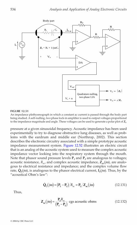
534 Analysis and Application of Analog Electronic Circuits
pressure at a given sinusoidal frequency. Acoustic impedance has been usedexperimentally to try to diagnose obstructive lung diseases, as well as prob-lems with the eardrum and middle ear (Northrop, 2002). This sectiondescribes the electronic circuitry associated with a simple prototype acoustic
that is an analog of the acoustic system used to measure the complex acousticimpedance vector looking into the respiratory system through the mouth.Note that phasor sound pressure levels P1 and P2 are analogous to voltages;acoustic resistance, Rac, and complex acoustic impedance, Zac(jw), are analo-gous to electrical resistance and impedance; and the complex volume flowrate, ·
Q2(jw), is analogous to the phasor electrical current, I2(jw). Thus, by the“acoustical Ohm’s law”:
(12.131)
Thus,
(12.132)
FIGURE 12.51An impedance plethysmograph in which a constant ac current is passed through the body partbeing studied. A self-nulling, two phase lock-in amplifier is used to output voltages proportionalto the impedance magnitude and angle. These voltages can be used to generate a polar plot of Zt.
Is
RF
R
R
Quadrature-nulling,two-phase LIA
Vref
Vs + n
Vp ∝ Zt
Vϕ ∝ ∠Zt
DA
Is
Body part
Zt = Rt + 1/jωCt
Vo+ −
Rt Ct
Q P P P Z1 2 2 ac2 j R jacw w( ) = -( ) = ( )
ZP
P Pac2
1 2
jRacw( ) =-( ) cgs acoustic ohms
© 2004 by CRC Press LLC
impedance measurement system. Figure 12.52 illustrates an electric circuit
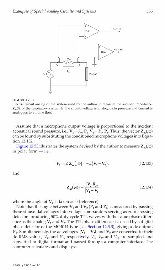
Examples of Special Analog Circuits and Systems 535
Assume that a microphone output voltage is proportional to the incidentacoustical sound pressure, i.e., V2 = Km P2, V1 = Km P1. Thus, the vector Zac(jw)can be found by substituting the conditioned microphone voltages into Equa-tion 12.132.
ac(jw)in polar form — i.e.,
(12.133)
and
(12.134)
where the angle of V2 is taken as 0 (reference).Note that the angle between V1 and V2 (P1 and P2) is measured by passing
these sinusoidal voltages into voltage comparators serving as zero-crossingdetectors producing 50% duty cycle TTL waves with the same phase differ-ence as the analog V1 and V2. The TTL phase difference is sensed by a digital
Vq. Simultaneously, the ac voltages (V1 - V2) and V2 are converted to theirdc RMS values, VQ and VP, respectively. Vq, VP, and VQ are sampled andconverted to digital format and passed through a computer interface. Thecomputer calculates and displays:
FIGURE 12.52Electric circuit analog of the system used by the author to measure the acoustic impedance,Zac(f), of the respiratory system. In the circuit, voltage is analogous to pressure and current isanalogous to volume flow.
∑Q2
P2P1
P1 Zac(jw)
V2 µ P2
∑
VQ µ Q2
DA2
DA1
Rac
V jq wµ ( ) = - -( )Z V Vac 1 2 ,
ZV
V Vac2
1 2
jRacw( ) µ
-
© 2004 by CRC Press LLC
Figure 12.53 illustrates the system devised by the author to measure Z
phase detector of the MC4044 type (see Section 12.3.3), giving a dc output,
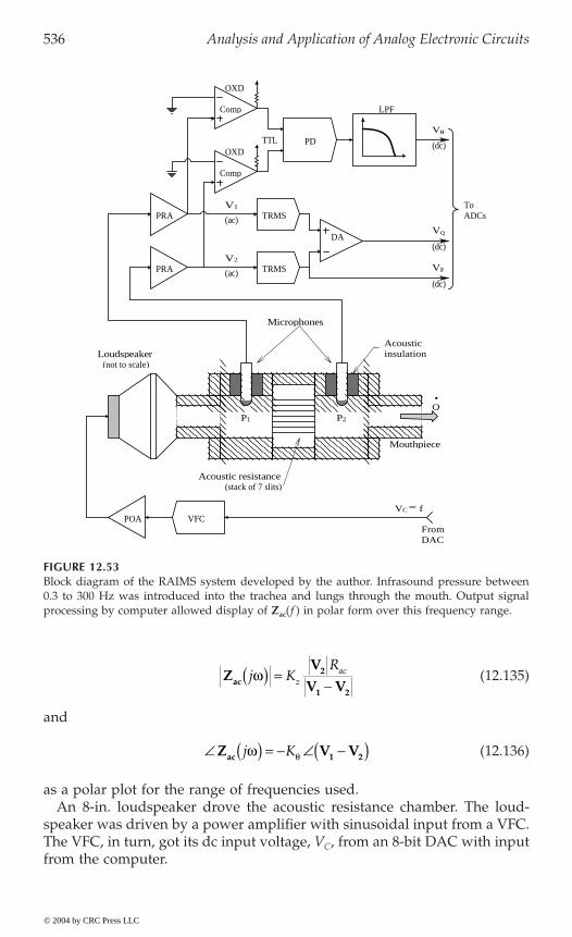
536 Analysis and Application of Analog Electronic Circuits
(12.135)
and
(12.136)
as a polar plot for the range of frequencies used.An 8-in. loudspeaker drove the acoustic resistance chamber. The loud-
speaker was driven by a power amplifier with sinusoidal input from a VFC.The VFC, in turn, got its dc input voltage, VC, from an 8-bit DAC with inputfrom the computer.
FIGURE 12.53Block diagram of the RAIMS system developed by the author. Infrasound pressure between0.3 to 300 Hz was introduced into the trachea and lungs through the mouth. Output signalprocessing by computer allowed display of Zac(f ) in polar form over this frequency range.
OXD
OXD
DA
POA VFC
Mouthpiece
VC ∝ f
Acoustic resistance
(not to scale)
P1 P2
(stack of 7 slits)
Loudspeaker
FromDAC
Comp
Microphones
Acousticinsulation
•
Q
Comp
LPF
PDVθ
VP
(dc)
(dc)
TRMSToADCs
TTL
(dc)
(ac)VQ
(ac) TRMSPRA
PRAV1
V2
ZV
V Vac2
1 2
j KR
zacw( ) =
-
( ) = - -( )Z V Vac 1 2j Kw q
© 2004 by CRC Press LLC
Examples of Special Analog Circuits and Systems 537
A critical part of the design was the acoustic resistance, Rac, across whichthe sound pressure drop was assumed to be without phase shift over theoperating frequency range of the instrument, i.e., Rac was real over the fre-quency range. Many “pure” acoustical resistances, such as those used inpneumotachs, etc., are made from many parallel capillary tubes. Capillarytubes’ acoustic resistance is real up to some frequency at which they beginlooking inductive due to the acoustic inertness of the tubes (Olson, 1940).To extend the range of real Rac, a stack of (parallel) thin slits with rectangularcross sections was used. It can be shown (Northrop, 2002) that the Rac of slitsremains real to a frequency significantly higher than that for an equivalentRac made from capillary tubes. This RAIMS system was designed to operatefrom 0.3 to 300 Hz. An earlier system described by Pimmel et al. (1977) thatused a commercial capillary-tube pneumotach for Rac had a high frequencylimit of 16 Hz before the pneumotach turned significantly reactive.
The prototype RAIMS system described here worked well with phantomacoustic lung impedances and normal volunteers in the lab, but was notinvestigated clinically.
12.9 Chapter Summary
Four diverse examples were chosen to illustrate the use of analog electroniccircuit ICs in biomedical instrumentation system design:
1. The microdegree polarimeter represents an instrument that hasevolved from a manually nulled instrument, with limited sensitivityto the optical rotation angle caused by polarized light passingthrough an optically active medium, to a closed-loop optoelectronicsystem with microdegree sensitivity. The optical rotation is used tomeasure D-glucose concentration in clear liquids. In the author’sdesign, an expensive Faraday rotator was eliminated; instead thewater solvent of the test solution was used for the Faraday medium.
2. Also developed was a closed-loop laser velocimeter and rangingsystem in which a CW laser beam was sinusoidally amplitude mod-ulated (instead of using pulsed laser light and measuring nanosec-ond delays in the return reflection). The frequency of the amplitudemodulations was automatically adjusted so that the phase differencebetween the transmitted and received modulations was held con-stant. This LAVERA system gave two simultaneous analog outputsproportional to target range and velocity; it was designed as a proto-type aid for blind persons.
3. The third system described was a self-balancing impedance plethys-mograph designed to measure small changes in volume as changes
© 2004 by CRC Press LLC
538 Analysis and Application of Analog Electronic Circuits
in admittance in certain anatomical regions, such as the chest or legs.This system operated at a constant 75 kHz and used feedback to nullan error voltage between the applied voltage and a voltage propor-tional to the body part’s admittance at a standard condition. It wasused to detect respiration and heartbeat simultaneously in an exper-imental context.
4. The fourth system was a respiratory acoustic impedance measure-ment system (RAIMS) — a prototype instrument intended to detectobstructive lung disease by comparison with “normal” records. Theacoustic driving point impedance was defined and the acousticequivalent of the voltmeter–ammeter method of measuring electricalimpedance was described. An acoustic pressure source (analogousto a voltage) from a loudspeaker forced acoustic volume flowthrough a real acoustic resistance and then the unknown acousticimpedance of the respiratory system (pharynx, trachea, bronchialtubes, and alveoli). Specially modified microphones were used tosense the driving-point pressure at the mouth, P2, and the volumeflow proportional to pressure difference to across the acoustical resis-tance,
·Q2 = (P1 ----P2)/Rac. Instrument display was in polar form: Zac(f)
vs. Zac(f) over 0.3 £ f £ 300 Hz.
© 2004 by CRC Press LLC

539
References
Allen, P.E. and D.R. Holberg. 2002. CMOS Analog Circuit Design. Oxford UniversityPress, New York.
Analog Devices. 1994. Design-In Reference Manual. Analog Devices, Norwood, MA.Angelo, E.J., Jr. 1969. Electronics: BJTs, FETs and Microcircuits. McGraw–Hill, New York.ARRL Staff. 1953. The Radio Amateur’s Handbook. American Radio Relay League, W.
Hartford, CT. Aseltine, J.A. 1958. Transform Method in Linear System Analysis. McGraw–Hill, New
York.Balanis, C.A. 1989. Advanced Engineering Electromagnetics. John Wiley & Sons, New
York.Barnes, J.R. 1987. Electronic System Design: Interference and Noise Control Techniques.
Prentice–Hall, Englewood Cliffs, NJ.Blanchard, A. 1976. Phase-Locked Loops. John Wiley & Sons, New York.Boylstead, R. and L. Nashelsky. 1987. Electronic Devices and Circuit Theory, 4th ed.
Prentice–Hall, Englewood Cliffs, NJ.Browne, A.F., T.R. Nelson, and R.B. Northrop. 1997. Microdegree polarimetric mea-
surement of glucose concentrations for biotechnology applications, in Proc. 23rdAnn. Northeast Bioengineering Conf. J.R. Lacourse, Ed. UNH/Durham5/21,22/97, pp. 9–10.
Cameron, B.D. and G.L. Coté. 1997. Noninvasive glucose sensing utilizing a digitalclosed-loop polarimetric approach. IEEE Trans. Biomed. Eng. 44(12): 1221–1227.
Chen, W.-K. 1986. Passive and Active Filters: Theory and Implementation. John Wiley &Sons, New York.
Chirlian, P.M. 1981. Analysis and Design of Integrated Electronic Circuits. Harper & Row,New York.
Clarke, K.K. and D.T. Hess. 1971. Communication Circuits: Analysis and Design. Add-ison–Wesley, Reading, MA.
Coté, G.L., M.D. Fox, and R.B. Northrop. 1992. Noninvasive optical polarimetricglucose sensing using a true phase measurement technique. IEEE Trans. Biomed.Eng. 39(7): 752–756.
Deliyannis, T., Y. Sun, and J.K. Fiddler. 1998. Continuous-Time Active Filter Design.CRC Press, Boca Raton, FL.
Dorf, R.C. 1967. Modern Control Systems. Addison-Wesley, Reading, MA.Du, Z. 1993. A Frequency-Independent, High Resolution Phase Meter. MS dissertation
in Biomedical Engineering, University of Connecticut, Storrs (R.B. Northrop,major adviser).
Eisner Safety Consultants. 2001. Overview of IEC60601-1 Medical Electrical Equipment.
Exar Integrated Systems, Inc. 1979. Phase-Locked Loop Data Book. Sunnyvale, CA.
© 2004 by CRC Press LLC
http:www.EisnerSafety.com.

540 Analysis and Application of Analog Electronic Circuits
Franco, S. 1988. Design with Operational Amplifiers and Integrated Circuits.McGraw–Hill, New York.
Gardner, F.M. 1979. Phaselock Techniques. 2nd ed. John Wiley & Sons, New York.Ghaussi, M.S. 1971. Electronic Circuits. D. Van Nostrand Co., New York.Gilham, E.J. 1957. A high-precision photoelectric polarimeter. J. Sci. Instrum. 34:
435–439.Goldwasser, S.M. 2001. Diode Lasers. 103 pp. Web article (Sam’s Laser FAQ).
Gray, P.R. and R.G. Meyer. 1984. Analysis and Design of Analog Integrated Circuits. JohnWiley & Sons, New York.
Grebene, A.B. 1971. The monolithic phase-locked loop — a versatile building block.IEEE Spectrum. March, 38–49.
Guyton, A.C. 1991. Textbook of Medical Physiology, 8th ed. W.B. Saunders, Philadelphia.Hannaford, B. and S. Lehman. 1986. Short-time Fourier analysis of the electromyo-
gram: fast movements and constant contraction. IEEE Trans. Biomed. Eng. 33(12):1173–1181.
Hecht, E. 1987. Optics, 2nd ed. Addison–Wesley, Reading, MA.Herzel, F., H. Erzgräber, and P. Weger. 2001. Integrated CMOS wideband oscillator
for RF applications. Electron. Lett. 37(6).Hodgkin, A.L. and A.F. Huxley. 1952. A quantitative description of membrane current
and its application to conduction and excitation in nerve. J. Physiol. (London).117: 500–544.
Huelsmann, L.P. 1993. Active and Passive Analog Filter Design: An Introduction.McGraw–Hill, New York.
James, H.J., N.B. Nichols, and R.S. Philips. 1947. Theory of Servomechanisms.McGraw–Hill, New York.
Kanai, H., K. Noma, and J. Hong. 2001. Advanced spin-valve GMR-head. Fujitsu Sci.Tech. J. 37(2): 174–182.
Kandel, E.R., J.H. Schwartz, and T.M. Jessel. 1991. Principles of Neural Science, 3rd ed.Appleton and Lange, Norwalk, CT.
Katz, B. 1966. Nerve, Muscle and Synapse. McGraw-Hill, New York.Kitchin, C. and L. Counts. 1983. RMS to DC Conversion Application Guide. Analog
Devices Inc., Norwood, MA.Kollár, I. 1986. The noise model of quantization. Proc. IMEKO TC4 Symp., Noise
Electric. Measurements. Como, Italy. June 19–21, 1986. OMIKK-Technoinform,Budapest, 1987, 125–129.
Krauss, J.D. 1953. Electromagnetics. McGraw–Hill, New York.Kuo, B.C. 1982. Automatic Control Systems, 4th ed. Prentice–Hall, Englewood Cliffs, NJ.Lancaster, D. 1996. Lancaster’s Active Filter Cookbook, 2nd ed. Butterworth–Heinemann,
Oxford, U.K.Lavallée, M., O.F. Schanne, and N.C. Hébert. 1969. Glass Microelectrodes. John Wiley
& Sons, New York.Lion, K.S. 1959. Instrumentation in Scientific Research: Electrical Input Transducers. McGraw-
Hill, New York.McDonald, B.M. and R.B. Northrop. 1993. Two-phase lock-in amplifier with phase-
locked loop vector tracking, in Proc. Euro. Conf. Circuit Theory and Design. Davos,Switzerland, 30 Aug.–3 Sept. 6 pp.
Mentelos, R.M. 2003. Electrical Safety in PC Based Medical Products. App. Note. AN-
© 2004 by CRC Press LLC
http://www.laserfaq.com/laserdio.htm.
10. RAM Technologies LLC, Guilford, CT. http://www.ramtechno.com

References 541
Merck Manual of Diagnosis and Therapy, 17th ed. (Centennial ed.). M.H. Beers and
Millman, J. 1979. Microelectronics. McGraw–Hill, New York.Nanavati, R.P. 1975. Semiconductor Devices: BJTs, JFETs, MOSFETs, and Integrated Cir-
cuits. Intext Educational Publishers, New York.Nelson, T.R. 1999. Development of a Type 1 Nonlinear Feedback System for Laser
Velocimetry and Ranging. MS dissertation in Biomedical Engineering, Univer-sity of Connecticut, Storrs (R.B. Northrop, major adviser).
Nise, N.S. 1995. Control Systems Engineering. Benjamin Cummings, Redwood City, CA.Northrop, R.B. and E.F. Guignon. 1970. Information processing in the optic lobes of
the lubber grasshopper. J. Insect Physiol. 16: 691–713.Northrop, R.B. and H.J. Grossman. 1974. An integrated-circuit pulse-height discrim-
inator with multiplexed display. J. Appl. Physiol. 37(6): 946–950.Northrop, R.B. 1990. Analog Electronic Circuits: Analysis and Applications. Addison–
Wesley, Reading, MA.Northrop, R.B. 1997. Introduction to Instrumentation and Measurements. CRC Press,
Boca Raton, FL.Northrop, R.B. 2000. Endogenous and Exogenous Regulation and Control of Physi-
ological Systems. CRC Press, Boca Raton, FL.Northrop, R.B. 2001. Introduction to Dynamic Modeling of Neuro-Sensory Systems. CRC
Press, Boca Raton, FL.Northrop, R.B. 2002. Non-Invasive Instrumentation and Measurements in Medical Diag-
nosis. CRC Press, Boca Raton, FL.Northrop, R.B. 2003. Signals and Systems Analysis in Biomedical Engineering. CRC Press,
Boca Raton, FL.Ogata, K. 1990. Modern Control Engineering, 2nd ed. Prentice–Hall, Englewood Cliffs, NJ.Olson, H.F. 1940. Elements of Acoustical Engineering. D. Van Nostrand Co., New York.Ott, H.W. 1976. Noise Reduction Techniques in Electronic Systems. John Wiley & Sons,
New York.Pallàs-Areny, R. and J.G. Webster. 2001. Sensors and Signal Conditioning, 2nd ed. John
Wiley & Sons, New York.
Phillips, C.L. and H.T. Nagle. 1994. Digital Control System Analysis and Design. 3rd ed.Prentice–Hall, Englewood Cliffs, NJ.
Pimmel, R.L. et al. 1977. Instrumentation for measuring respiratory impedance byforced oscillations. IEEE Trans. Biomed. Eng. 24(2): 89–93.
Plonsey, R. and D.G. Fleming. 1969. Biolelectric Phenomena. McGraw–Hill, New York.Proakis, J.G. and D.G. Manolakis. 1989. Introduction to Digital Signal Processing. Mac-
millan, New York.Rabinovitch, B., W.F. March, and R.L. Adams. 1982. Noninvasive glucose monitoring
of the aqueous humor of the eye. I. Measurements of very small optical rota-tions. Diabetes Care 5(3): 254–258.
Schaumann, R. and M.E. Van Valkenburg. 2001. Design of Analog Filters. OxfordUniversity Press.
Schilling, D.L. and C. Belove. 1989. Electronic Circuits: Discrete and Integrated, 3rd ed.McGraw-Hill College Division, New York.
© 2004 by CRC Press LLC
R. Berkow, Eds. http://www.merck.com/pubs/mmanual/section20/chap-ter277/277a.htm.
Newport Photonics. 2003. Laser Diode Testing. A tutorial. http://www.newport.com.
Perkin-Elmer. 2003. Avalanche Photodiodes: A User’s Guide. http://optoelectronics.perk-inelmer.com/library/papers/tp5.htm.

542 Analysis and Application of Analog Electronic Circuits
Soltani, P.K., D. Wysnewski, and K. Swartz. 1999. Amorphous selenium direct radi-ography for industrial imaging. Paper 22. Proc. Conf. Computerized Tomog-raphy for Industrial Applications and Image Processing in Radiology. 15–17March, Berlin, 123–132.
Stapleton, H. and A. O’Grady. 2001. Isolation techniques for high-resolution dataacquisition systems. EDN. 1 Feb.
Stark, H., F.B. Tuteur, and J.B. Anderson. 1988. Modern Electrical Communications,2nd ed. Prentice-Hall, Englewood Cliffs, NJ.
Stark, L. 1988. Neurological Control Systems. Plenum Press, New York.van der Ziel, A. 1974. Introductory Electronics. Prentice-Hall, Englewood Cliffs, NJ.Webster, J.G., Ed. 1992. Medical Instrumentation, 2nd ed. Houghton–Mifflin, Boston.West, J.B., Ed. 1985. Best and Taylor’s Physiological Basis of Medical Practice, 11th ed.
Williams & Wilkins, Baltimore.Wilson, W.L., Jr. 1996. A Sensitive Magnetoresistive MEMS Acoustic Sensor. Final
Report. Contract #961004. Rice University, Houston, TX.Yang, E.S. 1988. Microelectronic Devices. McGraw–Hill, New York.Ziemer, R.E. and W.H. Tranter. 1990. Principles of Communications: Systems, Modulation,
and Noise, 3rd ed. Houghton–Mifflin, Boston.
© 2004 by CRC Press LLC