
Analog VLSI Systems for Image Acquisition and Fast...
15
International Journal of Computer Vision, 8:3, 217-230 (1992) © 1992 Kluwer Academic Publishers, Manufactured in The Netherlands. Analog VLSI Systems for Image Acquisition and Fast Early Vision Processing JOHN L. WYATT, JR., CRAIG KEAST, MARK SEIDEL, DAVID STANDLEY, BERTHOLD HORN, TOM KNIGHT, CHARLES SODINI, HAE-SEUNG LEE, AND TOMASO POGGIO Massachusetts Institute of Technology, Department of Electrical Engineering and Computer Science, Cambridge, MA 02139 Received . Abstract This article describes a project to design and build prototype analog early vision systems that are remarkably low-power, small, and fast. Three chips are described in detail. A continuous-time CMOS imager and processor chip uses a fully parallel 2-D resistive grid to find an object's position and orientation at 5000 frames/second, using only 30 milliwatts of power. A CMOS/CCD imager and processor chip does high-speed image smoothing and segmentation in a clocked, fully parallel 2-D array. And a chip that merges imperfect depth and slope data to produce an accurate depth map is under development in switched-capacitor CMOS technology. 1 Introduction 1.1 Analog VLSI for Vision In real-time machine vision the sheer volume of image data to be acquired, managed, and processed leads both to very high computational demands and to communica- tion bottlenecks between imagers, memory, and proc- essors. Our group is designing and testing experimental analog VLSI systems to overcome these problems. The goal is to determine how the advantages of analog VLSI—high speed, low power, and small area—can be exploited and its disadvantages—limited accuracy, in- flexibility, lack of storage capacity, and long design and debugging times—can be minimized. The work is con- centrated on early vision tasks, that is, tasks early in the signal flow path of animal or machine vision. The faculty involved in this project since its begin- ning in September 1988 are Profs. Horn, Lee, Poggio, Sodini, and Wyatt, principal investigator. The com- pleted designs to date include seven different analog chips for image filtering and edge detection [1-3], mo- ment extraction to determine object position and orien- tation [4-6], image smoothing and segmentation [7-10], depth determination from stereo image pairs [II], accurate depth determination jointly from im- perfect depth and slope data [12], and camera motion determination [13], plus other chips to test novel cir- cuit designs or processing methods [7, 14, 15]. Some of these projects are now complete, while others are in various stages of testing, redesign, or refabrication. The typical subsystem is physically very small and can perform one or more computationally intensive image- processing tasks at hundreds to thousands of frames per second using only tens to hundreds of milliwatts. There is no single design strategy, but most systems have many of the following features: • sensors (typically on-chip) tightly coupled to the processing circuitry; • parallel computation; • analog circuits for high throughput, low latency, low power, and small area; • selection of tasks and algorithms requiring low to moderate precision; • special emphasis on computations that map naturally to physical processes in silicon, for example, to relax- ation processes or to resistive grids; • emphasis on charge-domain processing, for exam- ple, CCD and switched-capacitors, for maximal layout density and compatibility with CCD sensors;
Transcript of Analog VLSI Systems for Image Acquisition and Fast...
International Journal of Computer Vision, 8:3, 217-230 (1992)© 1992 Kluwer Academic Publishers, Manufactured in The Netherlands.
Analog VLSI Systems for Image Acquisition and Fast Early VisionProcessing
JOHN L. WYATT, JR., CRAIG KEAST, MARK SEIDEL, DAVID STANDLEY, BERTHOLD HORN,TOM KNIGHT, CHARLES SODINI, HAE-SEUNG LEE, AND TOMASO POGGIOMassachusetts Institute of Technology, Department of Electrical Engineering and Computer Science,Cambridge, MA 02139
Received .
AbstractThis article describes a project to design and build prototype analog early vision systems that are remarkablylow-power, small, and fast. Three chips are described in detail. A continuous-time CMOS imager and processorchip uses a fully parallel 2-D resistive grid to find an object's position and orientation at 5000 frames/second,using only 30 milliwatts of power. A CMOS/CCD imager and processor chip does high-speed image smoothingand segmentation in a clocked, fully parallel 2-D array. And a chip that merges imperfect depth and slope datato produce an accurate depth map is under development in switched-capacitor CMOS technology.
1 Introduction
1.1 Analog VLSI for Vision
In real-time machine vision the sheer volume of imagedata to be acquired, managed, and processed leads bothto very high computational demands and to communica-tion bottlenecks between imagers, memory, and proc-essors. Our group is designing and testing experimentalanalog VLSI systems to overcome these problems. Thegoal is to determine how the advantages of analogVLSI—high speed, low power, and small area—can beexploited and its disadvantages—limited accuracy, in-flexibility, lack of storage capacity, and long design anddebugging times—can be minimized. The work is con-centrated on early vision tasks, that is, tasks early inthe signal flow path of animal or machine vision.
The faculty involved in this project since its begin-ning in September 1988 are Profs. Horn, Lee, Poggio,Sodini, and Wyatt, principal investigator. The com-pleted designs to date include seven different analogchips for image filtering and edge detection [1-3], mo-ment extraction to determine object position and orien-tation [4-6], image smoothing and segmentation[7-10], depth determination from stereo image pairs
[II], accurate depth determination jointly from im-perfect depth and slope data [12], and camera motiondetermination [13], plus other chips to test novel cir-cuit designs or processing methods [7, 14, 15]. Someof these projects are now complete, while others arein various stages of testing, redesign, or refabrication.The typical subsystem is physically very small and canperform one or more computationally intensive image-processing tasks at hundreds to thousands of frames persecond using only tens to hundreds of milliwatts.
There is no single design strategy, but most systemshave many of the following features:
• sensors (typically on-chip) tightly coupled to theprocessing circuitry;
• parallel computation;• analog circuits for high throughput, low latency, low
power, and small area;• selection of tasks and algorithms requiring low to
moderate precision;• special emphasis on computations that map naturally
to physical processes in silicon, for example, to relax-ation processes or to resistive grids;
• emphasis on charge-domain processing, for exam-ple, CCD and switched-capacitors, for maximallayout density and compatibility with CCD sensors;

218 Wyatt, Keast, Seidel, Standley, Horn, Knight, Sodini, Lee and Poggio
• sufficiently fast processing that no long-term storagecircuitry is required;
• careful matching of algorithms, architecture, cir-cuitry, and (often custom) fabrication for maximumperformance; and
• modular design, with a standardized input and out-put, for compatibility between subsystems.
The advantages of this analog design approach toearly vision hardware are high speed (both in the senseof high throughput and low latency), low power, andsmall size and weight. High throughput can be impor-tant in high-speed inspection processes, for example,for printed materials or PC boards. Low latency is veryimportant for machine-vision-guided closed-loop feed-back systems, because they are easily destabilized byimage processing delays. Vehicle navigation and robotarm guidance are examples. Low power together withsmall size and weight are important for airborne andspace applications. And finally, small low-powersystems tend to be affordable.
1.2 System Design Issues
Analog systems are capable of very fast parallel opera-tion, operating directly on photosensor output signalswithout analog-to-digital conversion. But they offerlimited flexibility and precision. Simulations and ex-perimental chip tests have shown that analog precisionequivalent to 6-bit fixed-point arithmetic is adequatefor most algorithms that are suitable for analog im-plemenation. Our typical circuit design goal is 6-8 bitsprecision. These characteristics suggest that analog cir-cuits are of greatest value in preprocessing or earlyprocessing steps.
We believe that in some applications a high-speedvision system should consist of a photosensor arrayfollowed by an analog processing stage that feeds intoa digital processing section. The analog section out-puts should be of much lower bandwidth than the im-age input. For example, the analog output could con-sist of velocity measurements, image moments, orperhaps a line drawing. This output can be convertedto low-bandwidth digital form, easily handled by con-ventional digital technology.
For each of our designs the first decision is whetherit should be implemented as a single-chip system or asa modular component of a larger multichip system.Processing steps that output an entire grey-scale image
should generally be implemented as modules in a largersystem, especially if the image output needs furtherprocessing. But algorithms that convert an entire im-age into a few numbers are best implemented in single-chip systems. In our project these single-chip systemsare always focal-plane processors with the imager andprocessor on the same chip.
Chip-to-chip communication between componentsof a modular vision system is another systems designissue, especially since bandwidths are high and the set-tling times for analog signals are longer than for binarydata. We approach this problem by using wide com-muncation pathways between chips, each pathway con-sisting of N wires for NxM images, designed to com-municate one image column in parallel. Multichipmodules, in which the individual chips are mountedon a substrate inscribed with interconnect lines, wouldbe an ideal technology for this purpose and is underconsideration.
A third design issue is the degree of parallelism inprocessing. In fully parallel designs each pixel of anNxM array is associated with a distinct processor thatcommunicates directly with neighboring pixels andprocessors. These systems with order (NM) parallelismachieve very fast processing speed, often at a substan-tial cost in chip area. One possible difficulty is that insome cases only a small portion of chip area is leftavailable for sensors. These low fill-factor sensor ar-rays have reduced sensitivity due to the small opticallysensitive area, and their sparse sampling of the imagecan cause spatial aliasing problems. Another difficultyis that the processing speed often becomes so fast thatsystem delays are completely dominated by photosen-sor integration time and communication overhead, thatis, much of the processing speed becomes irrelevantto system performance. An alternative is to save areaat some cost in speed by having only one processor perimage row, that is, order (N) parallelism. These systemsprocess one image column at a time. They are par-ticularly convenient to design with CCD sensor arraysthat function as shift registers, carrying image data toa column of processors at the edge of the imager.
We have only attempted relatively small arrays, from29x29 to 64x64 pixels plus test arrays, in this pro-ject. These sizes are sufficient for examining the powerand limitations of analog design. Fabrication has beendone in the MOSIS 2-micron and MIT 1.75-micronprocesses. Many of the designs would scale directlywith fabrication dimensions, yielding 256x256 orlarger systems if fabricated in a commercial 0.8-micron
Analog VLSI Systems/or Image Acquisition and Fast Early Vision Processing 219
process. Arrays larger than 256x256 would generallyrequire system design changes. The single-chip systemscould be expanded by moving the imager to a separatechip, for example. The modular component systemscould be expanded by doing processing in parallel onseveral chips or handling portions of an image sequen-tially on a single chip.
Interestingly, most routes of expansion yield process-ing times that grow more slowly than the number ofpixels. For example a design dominated by processingtime that has order N parallelism and a designdominated by communication time that has column-parallel input and output would both have delays pro-portional only to M as the NxM pixel array is scaledup. And a design like the one in section 2 with speeddominated by photoreceptor response would have con-stant delay as the array size is increased.
1.3 Analog Design Styles
This project explores two very distinctstyles of analogdesign: continuous-time (i.e., unclocked) processingand discrete-time (i.e., clocked) processing. Both stylesare implemented primarily in CMOS (ComplementaryMetal Oxide Semiconductor) using field effect transis-tors (FETs). Bipolar transistors play only certain specialroles in our designs. The two varieties of clockeddesigns are based on charge-coupled devices (CCDs)and switched capacitors.
Unclocked analog systems are generally the fastestand require the least power. The unclocked designs inour project use bipolar transistors as photoreceptors andFETs for image processing. The bipolar transistors arecalled parasitic elements since they are unavoidablypresent in standard CMOS chips. These designs aresomewhat similar to those in Prof. Carver Mead's work[16]. One major difference is that we generally avoidoperating FETs in the subthreshold mode, to avoid tran-sistor matching problems and attain greater speed. Onecould also use photodiodes as sensors or bipolar tran-sistors as processing elements in unclocked designs.Since processing time is generally negligible in thesesystems (often less than 50 microseconds for an entireimage), the limiting factors for system speed arephotoreceptor response and image output times.
Many of our clocked designs use CCDs, the mostwidespread commercial electronic image sensor. Theyconvert incident optical energy into charge, and theycan also perform linear and thresholding operations that
are useful for image processing. CCD systems operatein discrete time on continous-valued packets of charge.Processing operations can be conveniently performeddirectly on the charge packets delivered by the photo-sensors. CCDs also provide the best form of analogshift register available. Charge decay times are longenough (on the order of tens of milliseconds for thesmallest detectable error in many systems at roomtemperature) that CCDs can serve as temporary storagedevices during processing. CCD systems typically re-quire a substantial number of clock signals (e.g., 10to 25 in our designs) that are produced off-chip. Thisis an advantage in that clock signals can be varied tocontrol the data flow, but it is also a significantdrawback in that clock generators consume power,clock signal routing consumes chip area, and the clock-ing operation adds complexity to the design.
Switched-capacitor (SC) systems are a second styleof discrete-time or clocked design. Switched capacitorswere originally introduced to synthesize on-chip linearresistors from capacitors and transistor switches. Theirimportance arises from their small area and the con-trollable conductance that is proportional to switchingfrequency. More complex multiterminal switched-capacitor elements that are useful in vision processingappear in section 4.
The circuit and system design issues mentionedabove are illustrated in three doctoral-level design pro-jects in the next three sections. David Standley's chipin section 2 is a fully parallel, continuous-time, CMOSsingle-chip system with bipolar phototransistors. CraigKeast's chip in section 3 is a fully parallel, discrete-time, CMOS/CCD system with CCD imagers that canbe used as a single-chip system or a modular systemcomponent. And Mark Seidel's design in section 4 willbe implemented as a fuly parallel, switched capacitor,CMOS modular system component chip that relies onan off-chip imager.
2 Fast Imager and Processor Chip for ObjectPosition and Orientation
David Standley, working with Profs. Horn and Wyatt,has designed and tested this analog VLSI chip, whichfinds the position and orientation of an object's imageagainst a dark background. The algorithm is based onfinding the first and second moments of the imagebrightness [17]. These moments allow the centroid (anindicator of position) and the axis of least inertia (an

220 Wyatt, Keast, Seidel, Standley, Horn, Knight, Sodini, Lee and Poggio
indicator of orientation) to be computed; see figure 1.If/Oc, y) is the intensity as a function of position, andwe (initially) assume that I(x, y) = 0 outside the ob-ject, then the required quantities are given by
f f I(x, y)h(x, y) dA (1)for all of the following h:
h(x, y) = 1, x, y, xy, x1 - y1 (2)(x2 and y2 are not needed separately). All of theweighting functions h are harmonic; that is, the Lapla-cian vanishes identically:
A/i(x, y) = 0 (3)
This observation is the key to a scheme proposed byHorn [18], in which an analog computer based on aresistive sheet (or resistor grid) can be constructed. Inthe implementation described here, an NxN array ofdiscrete intensity data is reduced to a set of 4N quan-tities by a 2-D resistor grid, and is subsequently reducedto a set of just eight quantities by 1-D resistor lines,all in a continuous-time, asynchronous fashion—noclocking required. The eight outputs can be digitized,and the centroid and orientation can be found using sim-ple expressions [4, ch. 2]. While earlier systems haveused this method to compute position [19, 20], nonehave used it previously to perform the orientation task,which requires computing second moments.
Fig. 1. Example of object centroid and axis of least inertia.
Figure 2 shows the resistor grid and its associated ar-ray of photoreceptor cells, which are uniformly spacedand occupy most of the chip area. The object imageis focused onto the surface of the chip, inside the ar-ray. Each photoreceptor cell contains a phototransistorand processing circuitry; it converts the incident light
centroid
photoreceptor cell
Fig. 2. Resistor grid and photoreceptor cell array.
intensity into a current that is injected into the grid.Thresholding is available to remove a dim (yet nonzero)scene background, so it does not interfere with thecalculation. If the intensity / at a particular cell is belowan adjustable threshold value /th> th6" no current is in-jected. If / > /th> men th® output current (which isanalogous to the gray-level weighting at that location)is proportional to / — 1^. The result is a continuous,piecewise-linear response characteristic. The array sizeis 29x29; intentional image blurring over a fewelements gives substantially increased resolution.
The perimeter of the grid is held at a constant voltageby the current buffers in figure 2: this ensures properoperation of the grid as a "data reduction" computer.The buffer outputs are simply copies of the currentsflowing into them from the grid. The buffers are neededto isolate the grid from the effects of other circuitry.Figure 3, which shows the complete architecture of thechip, indicates how the (copied) grid currents are fedinto resistor lines on the perimeter, how the ends ofthese lines are connected, and where the eight outputcurrents exit the chip near the corners. These currentsare measured by external circuitry which also holds theends of the lines at ground potential. In this setup, thereare two lines on each side: one uniform and one"quadratic" line. These calculate weighted sums of thegrid currents, where the weighting is (respectively) alinear or square-law function of the position along theline. The buffer outputs are steered either to the uniformor quadratic lines, so that four outputs are available ata time; that is, multiplexing is required here (but is notnecessary in general).

Analog VLSI Systems/or Image Acquisition and Fast Early Vision Processing 221
Fig. 3. Main chip architecture.
Working chips have been fabricated using theMOSIS service. The die size is 7.9 mm x 9.2 mm,and the imaging array is a 5.5 mm square. Accuracyis dependent on the object. For moderately sized andsufficiently elongated objects, for example, a diamondof diagonal dimensions 25 by 50 on a (normalized) 100by 100 image field, orientation is typically determinedto within ±2°. This fully parallel single-chip systemoperates at a remarkable speed of 5000 frames per sec-ond, and power consumption is typically only 30 mW.Further details of the design and testing can be foundin [4, 5, 6]. Dr. Standley is now designing a more ad-vanced version of this system with the imager and proc-essor on separate chips, at the Rockwell Corporation.
signal charge using standard CCD imaging techniques.The 2-dimensional Gaussian smoothing operation is ap-proximated by a discrete binomial convolution of theimage with a fully controllable support region. Thedesign incorporates segmentation circuits with variablethreshold control at each pixel location to preserveedges in the image. Once processed, the image is readout using a standard CCD clocking scheme.
By performing some of the image preprocessingfunctions in parallel on the image plane, the require-ments on subsequent signal processing circuits are re-duced. Since the area for collecting pixel charge is alarge fraction of the array, the need for a spatial anti-aliasing prefilter is eliminated, in contrast to many fullyparallel designs.
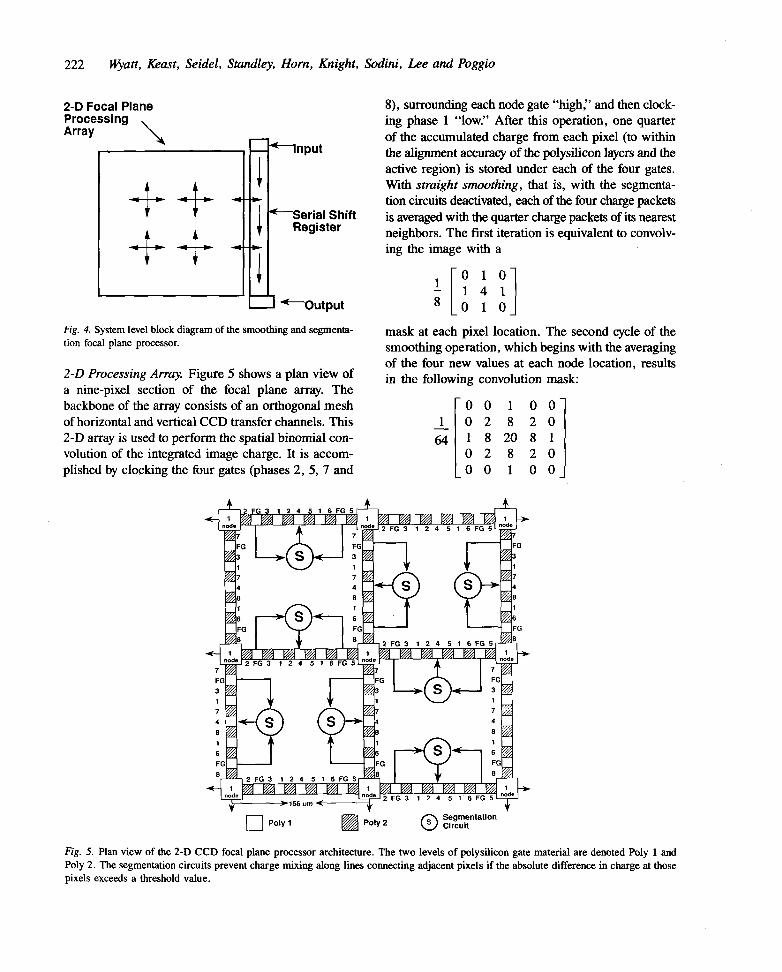
3 An Integrated Image Acquisition, Smoothing andSegmentation Focal Plane Processor
Craig L. Keast, working with Prof. Sodini, has de-signed and fabricated a focal plane processor for im-age acquisition, smoothing, and segmentation. Thetechnology used is CCD/CMOS, since it provides aconvenient way to image, process, and read out data.In this architecture, image brightness is transferred into
3.1 System Architecture
Figure 4 shows a system level block diagram of theprocessor. The system consists of four functionalblocks: the two-dimensional focal plane processing ar-ray, a conventional 4-phase CCD shift register, the out-put circuit, and an electrical input structure used fortesting and characterization.
222 Wyatt, Keast, Seidel, Standley, Horn, Knight, Sodini, Lee and Poggio
F—Serial ShiftRegister
2-D Focal PlaneProcessing .Array \^
Input
I •<—OutputFig. 4. System level block diagram of the smoothing and segmenta-tion focal plane processor.
2-D Processing Array. Figure 5 shows a plan view ofa nine-pixel section of the focal plane array. Thebackbone of the array consists of an orthogonal meshof horizontal and vertical CCD transfer channels. This2-D array is used to perform the spatial binomial con-volution of the integrated image charge. It is accom-plished by clocking the four gates (phases 2, 5, 7 and
8), surrounding each node gate "high," and then clock-ing phase 1 "low." After this operation, one quarterof the accumulated charge from each pixel (to withinthe alignment accuracy of the polysilicon layers and theactive region) is stored under each of the four gates.With straight smoothing, that is, with the segmenta-tion circuits deactivated, each of the four charge packetsis averaged with the quarter charge packets of its nearestneighbors. The first iteration is equivalent to convolv-ing the image with a
0 1 0'1 4 10 1 0
mask at each pixel location. The second cycle of thesmoothing operation, which begins with the averagingof the four new values at each node location, resultsin the following convolution mask:
0 0 1 0 00 2 8 2 01 8 20 8 10 2 8 2 00 0 1 0 0
J_64
L1^iii
i1^i
iG
i1
node^—————————>-156 um •<—————————±
I I poly1 III Poly 2
m m m m m ^'
FG
3
7
4
81
FQ
8
rJ2 FG 3
i
-] 2 FG 3
m m m m m m
-®-
r-®^\m m m m m.
1 2 4 5 1
( \
^ 1
1 2 4 5 1
i FG 5 -
'^l
6 FG 5
7
FG31748
6
FG8
^
1
1
1
i
i
ii^
i
i
i
1node
^ m m m m m2 FG ;
K'i
l2 FG 3
m m m m m7
317
4
81
6
FG
^ m m m m m-l2 F
^1- Q -l
r iY
G 3 1 2 4 5 1 6 F
© SegmentsCircuit
1 2 4 5 1
f 1
^ ^l ;
1 2 4 5 1
i FG 5 -,
'^k
6 FG 5r-
^
7
FG31
7
4
81
6
FG
8
• 5 ' - ,^
tion
^1
^7FC
1
ii6
FC
Is1
^
i
ii
1node
Fig. 5. Plan view of the 2-D CCD focal plane processor architecture. The two levels of polysilicon gate material are denoted Poly 1 andPoly 2. The segmentation circuits prevent charge mixing along lines connecting adjacent pixels if the absolute difference in charge at thosepixels exceeds a threshold value.
Analog VLSI Systems for linage Acquisition and Fast Early Vision Processing 223
Additional iterations of the smoothing cycle increasethe support region over which the convolution is per-formed. In its limit this operation approximates con-volution with a discrete Gaussian operator.
Smoothing with Segmentation. The binomial smooth-ing with segmentation is a nonlinear operation. It pre-serves high spatial frequencies associated with chargedifferences that are greater than the segmentationthreshold, while smoothing those differences that aresmaller than the threshold. In the CCD approach pre-sented here, the threshold of the segmentation circuitsis controlled by an externally adjustable voltage via aglobal bus.
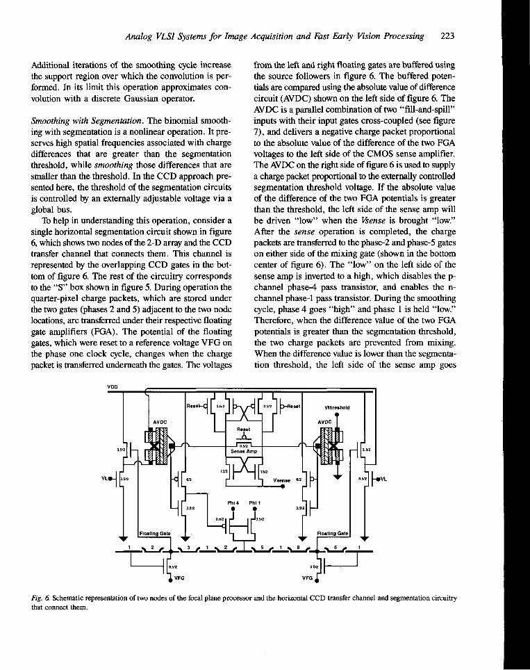
To help in understanding this operation, consider asingle horizontal segmentation circuit shown in figure6, which shows two nodes of the 2-D array and the CCDtransfer channel that connects them. This channel isrepresented by the overlapping CCD gates in the bot-tom of figure 6. The rest of the circuitry correspondsto the "S" box shown in figure 5. During operation thequarter-pixel charge packets, which are stored underthe two gates (phases 2 and 5) adjacent to the two nodelocations, are transferred under their respective floatinggate amplifiers (FGA). The potential of the floatinggates, which were reset to a reference voltage VFG onthe phase one clock cycle, changes when the chargepacket is transferred underneath the gates. The voltages
from the left and right floating gates are buffered usingthe source followers in figure 6. The buffered poten-tials are compared using the absolute value of differencecircuit (AVDC) shown on the left side of figure 6. TheA^DC is a parallel combination of two "fill-and-spill"inputs with their input gates cross-coupled (see figure7), and delivers a negative charge packet proportionalto the absolute value of the difference of the two FGAvoltages to the left side of the CMOS sense amplifier.The A^DC on the right side of figure 6 is used to supplya charge packet proportional to the externally controlledsegmentation threshold voltage. If the absolute valueof the difference of the two PGA potentials is greaterthan the threshold, the left side of the sense amp willbe driven "low" when the Vsense is brought "low."After the sense operation is completed, the chargepackets are transferred to the phase-2 and phase-5 gateson either side of the mixing gate (shown in the bottomcenter of figure 6). The "low" on the left side of thesense amp is inverted to a high, which disables the p-channel phase-4 pass transistor, and enables the n-channel phase-1 pass transistor. During the smoothingcycle, phase 4 goes "high" and phase 1 is held "low."Therefore, when the difference value of the two FGApotentials is greater than the segmentation threshold,the two charge packets are prevented from mixing.When the difference value is lower than the segmenta-tion threshold, the left side of the sense amp goes
Fig. 6. Schematic representation of two nodes of the focal plane processor and the horizontal CCD transfer channel and segmentation circuitrythat connect them.

224 Wyatt, Keast, Seidel, Standley, Horn, Knight, Sodini, Lee and Poggio
FG1 FG2 BG OG
ID-lnput DiodeFG1-Floating Gate 1
QO FG2-Floating Gate 2BG-Blocking GateOG-Output GateOD-Output Diode
"fill'
f'''"3^^ |———|"p"'" |—ligi-Essa Kij ^w-wi^ t2
t3
Rg. 7. Schematic plan view of the absolute value of difference circuitgate 1. A quantity of charge proportional to that difference is trapped
"high" and the phase-4 pass transistor is enabled,allowing the two charge packets to be averaged. Duringnormal operation, this cycle occurs in parallel alongall vertical and horizontal transfer channels resultingin true 2-dimensional processing.
3.2 Results
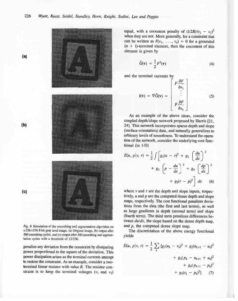
Craig Keast has also developed a 4-phase buried chan-nel CCD capability to enhance MIT's 1.75-micronbaseline CMOS process [9]. He has fabricated both a4x4 test array and a 40x40 pixel system in this proc-ess. The 4x4 array has been fully characterized andthe 40x40 system is currently under evaluation. Figure8 shows experimental data comparing the input imageand a series of processed images obtained from a 4x4processor test array after 1, 5, 10, 20, and 40 cycles.With a high segmentation threshold, none of the edgesare preserved and the processed images are identicalto the straight smoothing case; however, with a lowsegmentation threshold, the image edges are preserved.
Figure 9 shows the simulated results of thesmoothing and segmentation algorithm implemented on
(AVDC). Here the signal on floating gate 2 exceeds that on floatingunder gate 1 on the left and then dumped into the output diode.
a 256x256 8-bit image This figure shows the originalinput image, the image after 500 straight smoothingcycles, and the image after 500 smoothing and segmen-tation cycles with a threshold level of 12 out of a possi-ble 256 levels. With a pixel clock of 10 MHz and asegmentation clock of 1 MHz, images of this size couldbe processed at > 100 frames per second with 500smoothing and segmentation cycles per frame. Furtherdetails on this system can be found in [9, 10].
4 An SC Coupled Depth/Slope NetworkImplementation
Mark N. Seidel, working with Profs. Knight and Wyatt,has designed a switched-capacitor implementation ofHams' coupled depth/slope network [21]; it is currentlybeing fabricated. This network effects surface recon-struction by computing the dense depth and slope mapsgiven sparse depth and slope measurements; thesesparse measurements are outputs of other early visionmodules.
Because of the sparsity of the input data, there canbe infinitely many surfaces that might correspond to

Analog VLSI Systems for Image Acquisition and Fast Early Vision Processing 225
0
0
0
0
15
21
18
143
191
18
140
185
0
0
0
5
35
57
4
34
86
130
5
45
106
140
0
0
7
12
0
19
44
64
16
35
69
101
22
50
87
106
7
15
30
33
17
29
51
66
29
38
60
70
33
47
70
77
33
36
48
48
32
39
54
88
33
37
52
63
33
41
52
53
0
0
0
0
0
0
17
21
0
19
146
194
0
21
145
191
0
0
0
0
0
9
42
63
8
36
91
136
10
48
109
149
0
0
11
13
0
17
48
68
18
35
73
103
23
48
88
108
5
15
30
35
14
28
52
46
26
37
60
80
31
46
69
78
28
37
48
49
26
36
54
65
27
34
48
63
27
37
50
52
0
0
0
0
0
0
0
0
0
0
187
206
0
4
161
201
0
0
0
0
185
207
162
200
0
0
3
0
189
210
163
202
0
0
0
0
2
2
0
184
207
0
160
196
0
0
0
0
6
8
3
195
216
0
167
204
Fig. 8. Images obtained from a 4x4 processor test array. The input image (top) and a series of processed images obtained after 1, 5, 10,20, and 40 cycles: first row—straight smoothing, second row—smoothing with segmentation (high threshold), and third row—smoothing withsegmentation (low threshold). Below each row are the corresponding 8-bit intensity values.
the measurements. Alternatively, due to conflictingmeasurements, there might be no such solution. Ourapproach is to construct and minimize an energy func-tional consisting of terms penalizing deviation from theinput data as well as terms penalizing deviation froma measure of smoothness.
4.1 Implementing Cost Function Minimization
A beautiful application of analog resistor networks isin the implementation of cost function minimization.As a direct consequence of Maxwell's minimum heattheorem, reciprocal resistive networks have solutionscharacterized by an extremum principle, and therefore
appropriately designed networks automatically relax tothe minimum cost solution. Specifically, if the energyfunctional is constructed to represent the total resistivecocontent of the network, with each term representingthe cocontent [22] of a reciprocal resistive element, thenthe set of voltages and currents in the network (afterall transients die out) is that unique set that correspondsto the minimum total resistive cocontent. Since thisminimum cocontent also corresponds to the minimumof the cost function, the network solution is the solu-tion to the minimization problem.
Reciprocal resistive elements play an important rolein this theory, and constraint boxes [23, 24] allow oneto design and implement such elements in VLSI. Con-straint boxes are multiterminal resistive elements that
226 Wyatt, Keast, Seidel, Standley, Horn, Knight, Sodini, Lee and Poggio
(a)
(b)
(c)
Fig. 9. Simulation of the smoothing and segmentation algorithm ona 256x256 8-bit gray level image, (a) Original image, (b) output after500 smoothing cycles, and (c) output after 500 smoothing and segmen-tation cycles with a threshold of 12/256.
penalize any deviation from the constraint by dissipatingpower proportional to the square of the deviation. Thispower dissipation arises as the terminal currents attemptto restore the constraint. As an example, consider a two-terminal linear resistor with value R. The resistor con-straint is to keep the terminal voltages (v; and v^)
(4)
(5)
equal, with a cocontent penalty of (V2R) (v^ - v;)2
when they are not. More generally, for a constraint thatcan be written as F(VI, . . . , vj = 0 for a grounded(ra + l)-terminal element, then the cocontent of thiselement is given by
G(v) = ^(v)
and the terminal currents by9F_F9v,
i(v) = VG(v) =
9F_F9Vn
As an example of the above ideas, consider thecoupled depth/slope network proposed by Harris [21,24]. This network incorporates sparse depth and slope(surface orientation) data, and naturally generalizes toarbitrary levels of smoothness. To understand the opera-tion of the network, consider the underlying cost func-tional (in 1-D)
E(u,p\v,r)=^f^-v)2+g, W
C du^2 . Cdp^2\p-^} ^L^J+ 83 \P
+ 8s(r - p)2! dx (6)
where v and r are the depth and slope inputs, respec-tively, u and/? are the computed dense depth and slopemaps, respectively. The cost functional penalizes devia-tions from the data (the first and last terms), as wellas large gradients in depth (second term) and slope(fourth term). The third term penalizes differences be-tween du/dx, the slope based on the dense depth map,and p, the computed dense slope map.
The discretization of the above energy functionalyields
E(u, p\v, r) = - S bi("t - v*)2 + 82(.Uk+i - Uk)22 k
+ §3(Pk - Uk+i + Uk)2
+ g4(Pk+l - Pk)2
+ 8s(rk - Pk)2] (7)

Analog VLSI Systems for Image Acquisition and Fast Early Vision Processing 227
This functional represents the total cocontent of the net-work shown in figure 10. Four of the terms correspondto linear two-terminal resistors, and one (the gy term)corresponds to the subtracter constraint box. Theseboxes, indicated by circles in figure 10, attempt to en-force the constraint p^ = "t+i - u^ (or p = duldx inthe continuous case). The intuitive idea is that the depthdata (v) are smoothed by the depth input resistive net(resulting in u), while the slope data (r) are smoothedby the slope input resistive net (resulting in p). Thedepth and slope are coupled via the (bidirectional) con-straint boxes, and the network settles to its minimumenergy state.
C
Fig. 11. Parallel SC realization of a continuous resistor.
(where/ is the switching frequency and Tis the switch-ing period), and the current (charge transferred per unittime) is
Fig. 10. One-dimensional coupled depth/slope network.
i=^= fC^i - (8)
The equivalent resistance, therefore, is given by 2?eq =1//C. Typical values are C = 1 pf and/ = 1 MHz,yielding an equivalent resistance of 7?eq = 1 MO.
SC networks can also be thought of as discretizedversions of continuous time elements (or collections ofelements). For example, as observed by Tom Knightand Sandy Wells [unpublished], the SC network shownin figure 12(a) has the q-v characteristic
M=cF 1 -^ ML^J c L-i iJ L^J (9)
When one sets 4 = fq^ (where the overbar indicatesa time-averaged value) then the network is (in somesense) equivalent to that shown in figure 12(b) for which
4.2 The SC Coupled Depth/Slope Architecture
A straightforward implementation of figure 10 suffersfrom a few drawbacks. First, low-power dissipationdemands large resistor values that are difficult to ob-tain compactly in standard VLSI processes. Second,implementing the subtracter constraint box is nontrivial[23,24]. Third, controlling the relative resistor valuesis difficult in standard VLSI; this controllability allowsfor tailoring the network to the image in a dynamic way.For all of these reasons, we believe a switched-capacitor(SC) implementation is a viable alternative.
The basic parallel SC resistor equivalent is shownin figure 11. If the two terminals are connected tovoltage sources, then the charge transferred from ter-minal 1 to terminal 2 over one clock cycle is A<7 =C(vi - v-i). This charge transfers in time T = 1/f
(10)1-1
-11
Vl
-"2.i + R-,
Correspondence occurs when R^ + R^ = 1//C. Notethat this subcircuit implements the subtracter constraintbox, with the associated cocontent CK.VI, v^) =(/C/2)(V2 - vi)2.
4.3 The SC Implementation
A schematic of a portion of the network is shown infigure 13. The depth and slope input resistors (?i andgs) are implemented using the parallel SC resistorequivalents described earlier (Ci with ^3 and ^3 bar,and Cs with <^g and <f>s bar). The depth and slopesmoothing resistors (g^ and ^4) are implemented usinga double capacitor charge-sharing line with alternateclocking (C-i with <^i and <^>2, and €4 with <f>(, and (^7).

228 Wyatt, Keast, Seidel, Standley, Horn, Knight, Sodini, Lee and Poggio
^l ^2
(a)
1:1
V-
C equivalent to a transformer with loss, and (b) its continous-time
r(k-l) p(k-l) r(k) p(k)7 1 y y^H<1>7
^ ., - - 1
^Trr
\
L " T. T. " T.\(|>4 \(|>4 \<|>4 \lt)4
<!'.'
•T^
\(|)3 \<|)9
0 o
•?•
()).
J
'„I
-^
(b)
\(t>, \
^h
^
L±
"\9' \
<-] |
11^ 1
<t>2
-^——m-^,
4».r
„ i r^
^T(i>.t,0.
- /-'
rT
4
(^^
r. - / - - /•'L05
I
. - / - - --'
^
)
——————————————————————————<
\<t''
(()>
,
d^\
\1's
11cl 1
^
^T:•^3 \(|)9
1 6
())7
<)).
0.
v(k-l) u(k) v(k) u(k+l)
Fig. 13. SC 1-D coupled depth/slope switch-level schematic.
Analog VLSI Systems for Image Acquisition and Fast Early Vision Processing 229
The double capacitors representing each depth andslope node allow for simultaneous derivative sampling,as well as for symmetry of parasitic capacitances. Thesubtracter constraint box is also implemented using adouble capacitor (€3 with ^4 and <f>s). This doublingallows for an unbiased depth derivative and slopesampling. The ^9 switches allow for read-out of thedense depth and slope maps. Finally, by altering therelative clocking frequencies of the vairous subcircuits,the network response can be tailored dynamically.
Mark Seidel has designed a 1-D version of thissystem [12]. Test circuits are being fabricated in theMOSIS 2 micron CMOS processs.
5 Additional Designs and Related Projects
A more complete description of the MIT project canbe found in [25].
The first CCD system in this project was a 64x64imager and Laplacian of a Gaussian filter conceivedand designed by Woodward Yang in collaboration withDr. Alice Chiang of Lincoln Laboratories and Prof.Poggio [1-3]. This system component chip runs at 1000frames per second with order parallel processing (oneprocessor per image row) and produces a filtered im-age suitable for edge detection. He is currentlyredesigning this system for fabrication in a moremodern 2-micron process.
Mikko Hakkarainen, working with Prof. Lee, hasdesigned and tested a 40x40 CMOS/CCD stereo chip[11] that has been fabricated by MOSIS. It is based onthe computationally attractive Marr-Poggio-Dnimhelleralgorithm [26, 27].
Paul Yu and Prof. Lee have designed and tested anew compact CMOS resistive fuse circuit for contin-uous-time image smoothing and segmentation [7]. A32x32 array with phototransistor imagers has alsobeen designed and tested [8].
Ignacio McQuirk, working with Profs. Horn, Lee,and Wyatt, has designed and simulated a 64x64CMOS/CCD motion chip that finds the focus-of-expansion of a scene [13]. The algorithm is based ondirect methods for recovering motion without featureextraction [28]. The circuit components of this chiphave been fabricated by MOSIS and tested, and the en-tire chip is now under test.
Lisa Dron, working with Prof. Horn, has createdan image segmentation and compression algorithmdesigned for fully parallel implementation using CCDs
[29]. She has designed and is testing a chip to imple-ment this algorithm.
Chris Umminger, working with Prof. Sodini, hasdesigned and tested a switched-capacitor implementa-tion of resistive lines for use in image smoothing andsegmentation algorithms [15].
Steve Decker and Prof. Wyatt have designed an ex-tremely compact resistive fuse circuit using nonconven-tional depletion-mode CMOS. Mr. Decker, workingwith Prof. Sodini, has hand-fabricated and tested thissystem in MIT's Integrated Circuits Laboratory [7].
Andrew Lumsdaine, working with Prof. JacobWhite and Prof. Wyatt, has written a very fast, fullyparallel Connection-Machine-based simulator foranalog vision circuits and used it to study resistive fusesegmentation and smoothing circuits [30].
Mark Seidel, working with Prof. Wyatt, hasdiscovered a set of closed-form bounds for the settl-ing time of large-switched capacitor networks [31].
6 Conclusions
Analog VLSI systems offer some exciting performanceadvantages for early vision, particularly in the areasof speed, power, and size. We have found a speed ad-vantage of roughly l'/2 orders of magnitude over com-parable special-purpose digital systems, though thisfigure varies from example to example. The power andsize advantages should make analog systems cheaperin cases where their greater design, test, and debugg-ing costs can be amortized over large productionvolumes.
Since individual analog systems are not readilyreprogrammable, each early vision task requires aseparate design. A system consisting of several separatemodules can perform a number of distinct tasks, de-pending on the signal routing from one module toanother. The performance of initial designs, some ofwhich were reported here, leads us to expect that analogearly vision systems will find application in manyspecial niches where speed, power, size, or cost con-straints are crucial.
Acknowledgments
This work has been supported by NSF and DARPAunder Contract MIP-8814612 and by the DuPont Cor-poration, and NSF under contract MIP-9117724.

230 Wyatt, Keast, Seidel, Standley, Horn, Knight, Sodini, Lee and Poggio
References
1. W. Yang and A.M. Chiang, A full fill-factor CCD imager withintegrated signal processors, Proc. ISSCC, San Francisco, CA,pp. 218-219, February 1990.
2. W. Yang, The architecture and design of CCD processors forcomputer vision, Ph.D. thesis, Dept. Electrical Engineering andComputer Science, MIT, Cambridge, MA, August 1990.
3. W. Yang, Analog CCD processors for image filtering, SPIEIntern. Symp. on Opt. Eng. Photon. Aerospace Sensing, Orlando,FL, pp. 114-127, April 1991.
4. D.L. Standley, Analog VLSI implementation of smart visionsensors: Stability theory and an experimental design, Ph.D.thesis, Dept. Electrical Engineering and Computer Science, MIT,Cambridge, MA, P2, January 1991.
5. D.L. Standley and B.K.P. Horn, An object position and orien-tation 1C with embedded imager, Proc. IEEE Intern. Solid-StateCircuits Conf., San Francisco, CA, pp. 38-39, February 1991.
6. D.L. Standley, An object position and orientation 1C withembedded imager, IEEEJ. Solid-State Circ. 26(12): 1853-1859.
7. P.C. Yu, S.J. Decker, H.-S. Lee, C.G. Sodini, andJ.L. Wyatt,Jr., CMOS resistive fuses for image smoothing and segmenta-tion, IEEE J . Solid-State Circ. 27(4):545-553, April 1992.
8. P.C. Yu and H.-S. Lee, A CMOS resistive fuse processor for2-D image acquisition, smoothing and segmentation, submit-ted to 1992 European Solid-State Circuits Conference,Copenhagen, Denmark.
9. C.L. Keast and C.G. Sodini, An integrated image acquisition,smoothing and segmentation focal plane processor, to appearin VLSI Circuit Symposium, Seattle, WA, June 1992.
10. C.L. Keast, An integrated image acquisition, smoothing andsegmentation focal plane processor, Ph.D. Thesis, Departmentof Electrical Engineering and Computer Science, MTT, February1992.
11. M. Hakkarainen, J. Little, H.-S. Lee, and J.L. Wyatt, Jr., In-teraction of algorithm and implementation for analog VLSI stereovision, SPIE Symp. Opt. Eng. Photon. Aerospace Sensing,Orlando, FL, pp. 173-184, April 1991.
12. J.L. Wyatt, Jr., C. Keast, M. Seidel, D. Standley, B. Horn,T. Knight, C. Sodini, H.-S. Lee, and T. Poggio, Analog VLSIsystems for early vision processing, to appear in Proc. 1992IEEE Intern. Symp. on Circuits and Systems, May 1992, SanDiego, CA.
13. I.S. McQuirk, Direct methods for estimating the focus of ex-pansion in analog VLSI, S.M. thesis, Department of ElectricalEngineering and Computer Science, MIT, Cambridge, MA,September 1991.
14. C.L. Keast, and C.G. Sodini, A CCD/CMOS process for in-tegrated image acquisition and early vision signal processing,Proc. SPIE Charge-Coupled Devices and Solid State Sensors,Santa Clara, CA, pp. 152-161, February 1990.
15. C.B. Umminger and C.G. Sodini, Switched capacitor networksfor monolithic image processing systems, to appear in IEEETrans. Circ. Syst.
16. C. Mead, Analog VLSI and Neural Systems. Addison-Wesley:Reading, MA, 1989.
17. B.K.P. Horn, Robot Vision, MIT Press: Cambridge, MA, andMcGraw-Hill, New York, pp. 48-57, 1986.
18. B.K.P. Horn, Parallel networks for machine vision. In ResearchDirections in Computer Science: An MIT Perspective, A. Meyer,G.V. Guttag, R.L. Rivest, and P. Szolovits, eds., MIT Press:Cambridge, MA, pp. 531-572, 1991.
19. J.T. Wallmark, A new photocell using lateral photoeffect, Proc.Inst. Radio Engin. 45:474-483, April 1957.
20. S.P. DeWeerth and C.A. Mead, A two-dimensional visual track-ing array, Advanced Research in VLSI, J . Alien and F.T.Leighton, eds., MIT Press: Cambridge, MA, pp. 259-275,1988.
21. J.G. Harris, The coupled depth/slope approach to surfacereconstruction. Technical Report TR-908, MIT AI Laboratory,Cambridge, MA, June 1986.
22. J. Harris, C. Koch, J. Luo, andJ. Wyatt, Resistive fuses: Analoghardware for detecting discontinuities in early vision. In AnalogVLSI Implementation of Neural Systems, C. Mead and M. Ismail,eds., Kluwer Academic, Norwell, MA, pp. 27-55, 1989.
23. J.G. Harris, Analog models for early vision, Ph.D. thesis, CalTech, Pasadena, CA, 1991.
24. J.G. Harris, Solving early vision problems with VLSI constraintnetworks. In Neural Architectures for Computer Vision,AAAI-88 Workshop, Minneapolis, MN, August 1988.
25. B. Horn, H.-S. Lee, C. Sodini, T. Poggio, and J. Wyatt, Thefirst three years of the MIT vision chip project—Analog VLSIsystems for integrated image acquisition and early vision proc-essing, VLSI Memo No. 91-645, Microsystems TechnologyLaboratory, MIT, October 1991.
26. D. Marr and T. Poggio, Cooperative computation of stereodisparity. Science 194:283-287, October 1976.
27. M. Drumheller, and T. Poggio, On parallel stereo, Proc. IEEEIntern. Conf. Rob. Autom., San Francisco, 1986.
28. B.K.P. Horn and E.J.Weldon,Jr., Direct methods for recover-ing motion. Intern. J. Comput. Vis. 2(1):51-76, 1988.
29. L. Dron, The multi-scale veto model: A two-stage analog net-work for edge detection and image reconstruction, submittedto Intern. J. Comput. Vis.
30. A. Lumsdaine, J.L. Wyatt, Jr. and I.M. Elfadel, Nonlinearanalog networks for image smoothing and segmentation, J. VLSISig. Proc. 3:53-68, 1991.
31. M.N. Seidel and J.L. Wyatt, Jr., Settling-time bounds forswitched-capacitor networks, Proc. IMACS World cong. Com-put. Appl. Math. Dublin, Ireland, pp. 1669-1670, July 1991.

V o l u m e 8, N u m b e r 3, S e p t e m b e r 1992
INTERNATIONAL JOURNAL OF
COMPUTER VISION
C O N T E N T SSpecial Issue: VLSI for Computer VisionGuest Editor: James J. dark
Guest Editor Introduction, James J. dark..........................................................
A VLSI Pyramid Chip for Multiresolution Image AnalysisGooitzen S. van der Wal and Peter J. Burt..........................................................
Analog VLSI Circuits for Stimulus Localization and Centroid ComputationStephen P. DeWeerth.............................................................................................
Computing Motion Using Analog VLSI Vision Chips: An ExperimentalComparison Among Different ApproachesTimothy Horiuchi, Wyeth Bair, Brooks Bishofberger, John Lazzaro,Andrew Moore, and ChristofKoch ......................................................................
Analog VLSI Systems for Image Acquisition and Fast Early VisionProcessingJohn L. Wyatt, Jr., Craig Keast, Mark Seidel, David Standley, Berthold Horn,Tom Knight, Charles Sod'ini, Hae-Seung Lee, and Tomaso Poggio..................
Dynamic Wires: An Analog VLSI Model for Object-Based ProcessingShih-Chii Liu and John Harris..............................................................................092056919031992900048301
0920-5691(199209)8:3;1-F