Analog Integrated Circuit Design 2nd Editionhtang/ECE5211_doc_files/ECE5211_files/Chapter3.pdfsignal...
40
Today’s topic: 1. Basic current mirrors 2. single-stage amplifiers 3. differential amplifiers Chapter 3 1
Transcript of Analog Integrated Circuit Design 2nd Editionhtang/ECE5211_doc_files/ECE5211_files/Chapter3.pdfsignal...

Today’s topic: 1. Basic current mirrors
2. single-stage amplifiers 3. differential amplifiers
Chapter 3
1

The purpose of this Chapter is to discuss fundamental circuit building blocks. A good knowledge of these basic building blocks is critical to understanding many subjects to be discussed later. CMOS current mirrors and gain stages are emphasized here, while the general small-signal analysis method can be applied to BJT versions. When analyzing transistor circuits to determine their small-signal behavior, it is implicitly assumed that signals are small enough that linear approximations about an operating point (Q point) accurately reflect how the circuit operates. These linear approximations may be represented schematically by replacing transistors with small-signal equivalent circuit, whose parameters (such as gm, rds etc) are determined from the operating point. A note on notations in the book and the lecture:
2

A general procedure for small-signal analysis:
3

A general procedure for small-signal analysis:
4
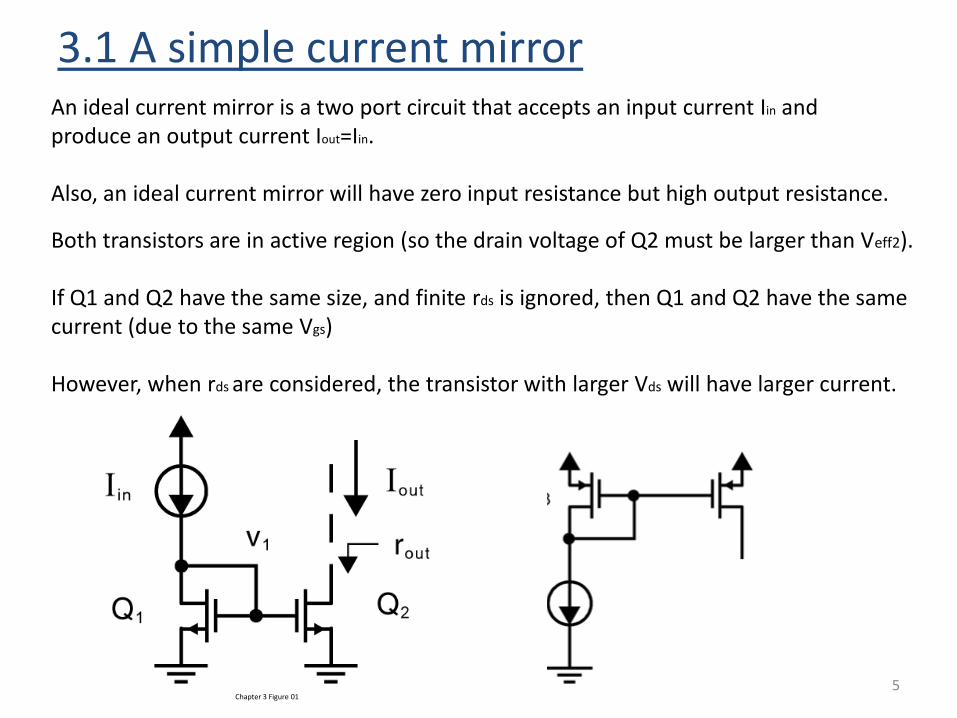
An ideal current mirror is a two port circuit that accepts an input current Iin and produce an output current Iout=Iin. Also, an ideal current mirror will have zero input resistance but high output resistance.
3.1 A simple current mirror
Chapter 3 Figure 01
Both transistors are in active region (so the drain voltage of Q2 must be larger than Veff2). If Q1 and Q2 have the same size, and finite rds is ignored, then Q1 and Q2 have the same current (due to the same Vgs) However, when rds are considered, the transistor with larger Vds will have larger current.
5

Chapter 3 Figure 02
A simple current mirror: input resistance We can use the following small-signal equivalent circuit to compute the input resistance of the current mirror. (Iin is open and low-frequency model is used). Then, apply a test signal voltage Vy at node V1 and measure the current iy
Input resistance is given by rin = Vy/iy = Q1 is sometimes referred to as a diode-connected transistor.
rin
rin
6

Chapter 3 Figure 03
A simple current mirror: output resistance Using the model for the input resistance from previous slides leads to a simplified small-signal equivalent circuit for the overall current mirror. .
Output resistance is given by rout=Vx/ix =rds2
7
Chapter 3 Figure 01
Vbias
rout = rds2
In this configuration, as long as gate terminal is small-signal ground, the resistance looking into the drain is rds2

Chapter 3 Figure 03
A simple current mirror: output resistance Using the model for the input resistance from previous slides leads to a simplified small-signal equivalent circuit for the overall current mirror. .
Output resistance is given by rout=Vx/ix =rds2
8

An example 3.1 (page 119)
9
Estimation using low-frequency small-signal linear equivalent circuit

Chapter 3 Figure 04
3.2 A common-source amplifier A common use of simple current mirrors is to be active loads in a single-stage amplifier. By using an active load, a high-impedance output load can be realized without using excessively large resistors or a large power supply voltage (for example, a 100k resistor load with 100μA bias current would need a power supply of at least 10V). The common-source (CS) topology is the most popular gain stage, especially when high input impedance is desired.
10
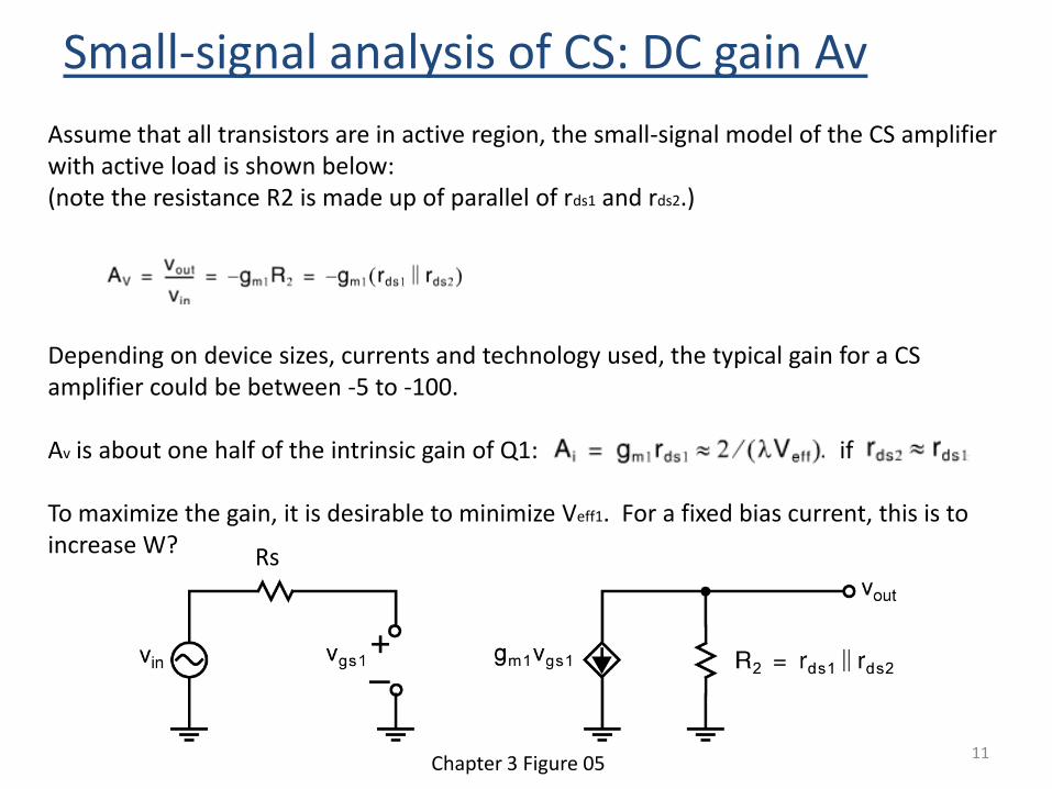
Chapter 3 Figure 05
Assume that all transistors are in active region, the small-signal model of the CS amplifier with active load is shown below: (note the resistance R2 is made up of parallel of rds1 and rds2.) Depending on device sizes, currents and technology used, the typical gain for a CS amplifier could be between -5 to -100. Av is about one half of the intrinsic gain of Q1: if To maximize the gain, it is desirable to minimize Veff1. For a fixed bias current, this is to increase W?
11
Rs
Small-signal analysis of CS: DC gain Av

Chapter 3 Figure 05
Chapter 3 Figure 04
rin
rin= rout=R2
12
Rs
Small-signal analysis of CS: rin and rout

An example 3.2 and 3.3 (page 121)
13

Chapter 3 Figure 06
Another general use of current mirrors is to supply the bias current for a common-drain or source follower (SF) amplifier. SF amplifiers are commonly used as voltage buffers.
3.3 A common-drain amplifier
14

Chapter 3 Figure 07
Small-signal analysis of SF amplifier: gain Av In the small-signal model, note that the voltage-controlled current source that models the body effect of MOS transistors is included as there is finite source-body voltage (unlike CS amplifier), which may become a major limitation on the small-signal gain. Note that the voltage-controlled current source modeling the body effect produces a current that is proportional to the voltage across it, which makes it equivalent to a resistor of 1/gs1. This allows to simplify the circuit to the right-hand side.
Chapter 3 Figure 08 15
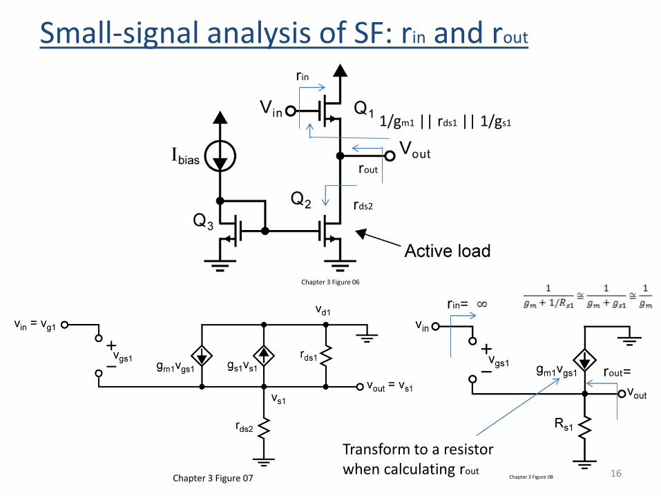
Chapter 3 Figure 07 Chapter 3 Figure 08
rout=
rin=
Chapter 3 Figure 06
rin
rout
16
Small-signal analysis of SF: rin and rout
rds2
1/gm1 || rds1 || 1/gs1
Transform to a resistor when calculating rout

Example 3.4 (page 123)
Hence, it can be seen that body-effect is the major source of error causing the gain of the SF amplifier to be less than 1.0.
17

Chapter 3 Figure 09
3.4 A common-gate amplifier A common-gate amplifier is used as a gain stage when small input impedance is desired. Also, it is often used when the input signal is a current as small input impedance is desired. Aside from its low input impedance, the common-gate amplifier is similar to a CS amplifier as the input signal is across Gate-Source terminal and output taken from the Drain terminal. Hence, in both amplifiers, the small signal gain equals the product of gm and total impedance at the drain.
18

Chapter 3 Figure 10
Chapter 3 Figure 11 19

Chapter 3 Figure 11
20
is

Chapter 3 Figure 11
21
Compare to Slide 16
Chapter 3 Figure 08
If RL=rds2=rds1, rin=2/gm1 for low frequency. If RL is even larger, then rin is more than 2/gm1.
Comparison of the impedances

Chapter 3 Figure 11
rout
Ix
Vx
Ix = Vx/RL – (gm1+gs1)Vs1 + (Vx-Vs1)/rds1
-(gm1+gs1)Vs1 + (Vx-Vs1)/rds1 = Vs1/Rs
If RL=rds2=rds1 and Rs=0, then not surprisingly rout=rds1/2
22
Small-signal analysis of CG: rout
1
1
1
1 ])(1[
dsL
Lds
ds
SSsm
X
Xout
rR
Rrr
RRgg
I
Vr

23
Example 3.5 (page 127)
Chapter 3 Figure 12
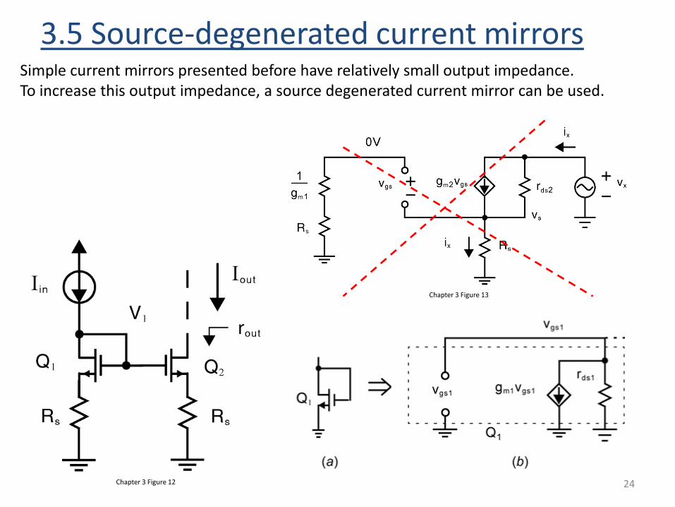
3.5 Source-degenerated current mirrors Simple current mirrors presented before have relatively small output impedance. To increase this output impedance, a source degenerated current mirror can be used.
24
Chapter 3 Figure 13

Chapter 3 Figure 13
Note that in the small-signal model to compute rout, (1) the gate voltage for both Q1 and Q2 is 0 as no small-signal current flows to the gate, (2) we neglect the body effect.
If body effect included
25
Compare to Slides 22
Small-signal model to find rout
gm1Vgs1 = Vgs1/rds1
0V

Therefore, compared to the simple two-transistor current mirror, the output impedance of source-degenerated current mirror has output impedance increased by a factor equal to (1+gm2Rs). Note also that such a formula can often be applied to moderately complicated circuits to quickly estimate the impedance looking into a node. 26
Example 3.6 (page 128)

Chapter 3 Figure 14
3.6 Cascode current mirrors Cascode current mirrors can be used to further increase the output impedance. Note that rout’ looking into the drain of Q2 is simply rds2. The rout looking into the drain of Q4, can be derived from the formula for source-degenerated current mirrors, by considering Q4 as a current source with a source-degenerated resistor of rds2 from Q2.
rout’
Thus, the output impedance is increased by a factor of gm4rds4, which is the gain of a single transistor. Such a large increase can be important to realize single-stage amplifiers with large gains. The drawback in using a cascode current mirror is the reduction of the maximum output voltage swing.
27

Chapter 3 Figure 14
rout’
vgs2
vgs4
Both are small-signal ground voltage 0
rin

Chapter 3 Figure 14
rout’
What is the minimum voltage at Vout to maintain Q2 and Q4 in active region? If we assume all transistors have the same sizes and currents, and therefore the same Vgsi=Veffi+Vtni, where i=1,2,3,4, then
So, the Vds2 for Q2 is larger than the minimum needed which is Veff2. Since the smallest output voltage VD4 can be VDS2+Veff2 before Q4 goes into triode region, so the minimum allowed voltage for Vout is The loss of signal swing is a serious drawback when modern analog IC are used with low power supply of 1V. (Later, we will see how to address this issue).
29
Minimum output voltage

Chapter 3 Figure 14
rout’
Example 3.7 (page 130)
So the minimum Vout is then 2Veff+ Vtn=0.98V, which 0.77V larger than the simple current mirror while rout is increased by 30 times.
30

Chapter 3 Figure 15
3.7 Cascode gain stage In modern IC design, a commonly used configuration for a single-stage amplifier is a cascode amplifier. This configuration consists of a CS transistor feeding into a CG one. In (a) below, both CS Q1 and cascode transistor Q2 are NMOS (telescopic-cascode amplifier) In (b), CS Q1 is NMOS and cascode transistor Q2 is PMOS (folded-cascode amplifier). Two major reasons for cascode stages: (1) they provide large gain when current sources are realized with cascode current mirrors; (2) they limit the voltage across Q1, minimizing short channel effects. The main drawback of cascode stages is that the output voltage swing is reduced in order to keep both Q1 and Q2 in active region when compared to the CS amplifier.
31

Chapter 3 Figure 16
The impedance looking into drain of Q2
The impedance looking into source of Q2
32
Small-signal model

Chapter 3 Figure 16
The gain in this case is only a factor of 2 larger than that for a common-source amplifier. Also, almost all of the gain is across Q2.
Example 3.9 (page 133)
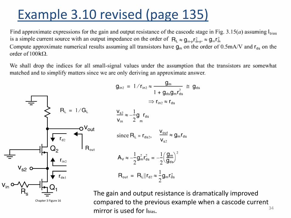
Chapter 3 Figure 16
The gain and output resistance is dramatically improved compared to the previous example when a cascode current mirror is used for Ibias. 34
Example 3.10 revised (page 135)

3.8 Differential pair and gain stage A differential pair have identically-sized and –biased transistors Q1 and Q2. It is usually used as the input stage of a Operational Amplifier.
35

Chapter 3 Figure 18
Small-signal model using T model To simplify the analysis, we ignore the output impedance of the transistors temporarily. Defining the differential input voltage as
36
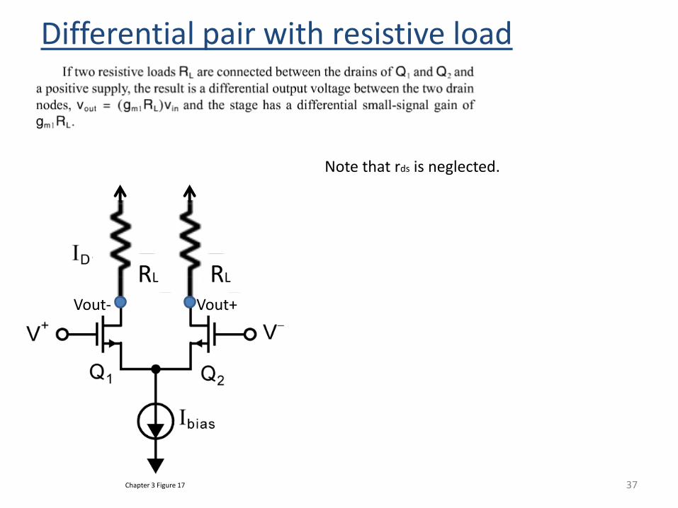
Chapter 3 Figure 17
Differential pair with resistive load
Vout+ Vout-
37
Note that rds is neglected.
RL RL

Chapter 3 Figure 19
Differential pair with current mirror As with the CS amplifier, we can replace the resistor by current mirrors as an active load. Then, a complete differential-input, single-ended output gain stage can be realized. This circuit is typically the first gain stage in a classical two-stage integrated OpAmp to be discussed later. From small-signal analysis of the differential pair,
How to determine the small-signal output resistance rout?
38

Chapter 3 Figure 20
T model was used for Q1, Q2 and diode-connected Q3 was replaced by an equivalent resistance and hybrid-pi model for Q4.
D3/G3/D1
Then assuming the effect of rds1 can be ignored (since it is much larger than rs1), then
39
Computing rout

Chapter 3 Figure 20
D3/G3/D1
40
Computing rout


![Circuit Network Analysis - [Chapter1] Basic Circuit Laws](https://static.fdocuments.us/doc/165x107/55ced242bb61eb192c8b480c/circuit-network-analysis-chapter1-basic-circuit-laws.jpg)