Analog electronics modern analog filter analysis & design a practical approach
364
Rabin Raut and M. N. S. Swamy Modern Analog Filter Analysis and Design
-
Upload
boging-bobit -
Category
Technology
-
view
1.581 -
download
23
Transcript of Analog electronics modern analog filter analysis & design a practical approach

Rabin Raut and M. N. S. Swamy
Modern Analog Filter Analysis and Design

Related Titles
Shenoi, B. A.
Introduction to Digital Signal Processingand Filter Design
2005
ISBN: 978-0-471-46482-2
Madsen, C. K., Zhao, J. H.
Optical Filter Design and AnalysisA Signal Processing Approach
1999
ISBN: 978-0-471-18373-0

Rabin Raut and M. N. S. Swamy
Modern Analog Filter Analysis and Design
A Practical Approach

The Authors
Dr. Rabin RautConcordia UniversityElectrical and Computer EngineeringMontreal, [email protected]
Dr. M. N. S. SwamyConcordia UniversityElectrical and Computer EngineeringMontreal, [email protected]
CoverSpieszdesign, Neu-Ulm, Germany
All books published by Wiley-VCH arecarefully produced. Nevertheless, authors,editors, and publisher do not warrant theinformation contained in these books,including this book, to be free of errors.Readers are advised to keep in mind thatstatements, data, illustrations, proceduraldetails or other items may inadvertently beinaccurate.
Library of Congress Card No.: applied for
British Library Cataloguing-in-PublicationDataA catalogue record for this book is availablefrom the British Library.
Bibliographic information published by theDeutsche NationalbibliothekThe Deutsche Nationalbibliotheklists this publication in the DeutscheNationalbibliografie; detailed bibliographicdata are available on the Internet at<http://dnb.d-nb.de>.
2010 WILEY-VCH Verlag & Co. KGaA,Boschstr. 12, 69469 Weinheim, Germany
All rights reserved (including those oftranslation into other languages). No partof this book may be reproduced in anyform – by photoprinting, microfilm, or anyother means – nor transmitted or translatedinto a machine language without writtenpermission from the publishers. Registerednames, trademarks, etc. used in this book,even when not specifically marked as such,are not to be considered unprotected by law.
Cover Design Adam Design, WeinheimTypesetting Laserwords Private Ltd.,Chennai, IndiaPrinting and Binding Fabulous Printers PteLtd, Singapore
Printed in SingaporePrinted on acid-free paper
ISBN: 978-3-527-40766-8

V
A student acquires a quarter of knowledge from the teacher, a quarter from self study,a quarter from class mates, and the final quarter in course of time.
From Neeti Sara
ToOur parents, teachers, and our wives Sucheta & LeelaandLate Prof. B. B. Bhattacharyya(Ph.D. supervisor of R. Raut andFirst Ph.D. student of M. N. S Swamy)
Modern Analog Filter Analysis and Design: A Practical Approach. Rabin Raut and M. N. S. SwamyCopyright 2010 WILEY-VCH Verlag GmbH & Co. KGaA, WeinheimISBN: 978-3-527-40766-8

VII
Contents
Preface XVAbbreviations XIX
1 Introduction 1
2 A Review of Network Analysis Techniques 72.1 Transformed Impedances 72.2 Nodal Analysis 92.3 Loop (Mesh) Analysis 92.4 Network Functions 112.5 One-Port and Two-Port Networks 122.5.1 One-Port Networks 122.5.2 Two-Port Networks 132.5.2.1 Admittance Matrix Parameters 132.5.2.2 Impedance Matrix Parameters 142.5.2.3 Chain Parameters (Transmission Parameters) 142.5.2.4 Interrelationships 152.5.2.5 Three-Terminal Two-Port Network 162.5.2.6 Equivalent Networks 162.5.2.7 Some Commonly Used Nonreciprocal Two-Ports 162.6 Indefinite Admittance Matrix 182.6.1 Network Functions of a Multiterminal Network 202.7 Analysis of Constrained Networks 242.8 Active Building Blocks for Implementing Analog Filters 282.8.1 Operational Amplifier 282.8.2 Operational Transconductance Amplifier 302.8.3 Current Conveyor 31
Practice Problems 33
3 Network Theorems and Approximation of Filter Functions 413.1 Impedance Scaling 413.2 Impedance Transformation 423.3 Dual and Inverse Networks 44
Modern Analog Filter Analysis and Design: A Practical Approach. Rabin Raut and M. N. S. SwamyCopyright 2010 WILEY-VCH Verlag GmbH & Co. KGaA, WeinheimISBN: 978-3-527-40766-8

VIII Contents
3.3.1 Dual and Inverse One-Port Networks 443.3.2 Dual Two-Port Networks 453.4 Reversed Networks 473.5 Transposed Network 483.6 Applications to Terminated Networks 503.7 Frequency Scaling 523.8 Types of Filters 523.9 Magnitude Approximation 543.9.1 Maximally Flat Magnitude (MFM) Approximation 553.9.1.1 MFM Filter Transfer Function 563.9.2 Chebyshev (CHEB) Magnitude Approximation 603.9.2.1 CHEB Filter Transfer Function 633.9.3 Elliptic (ELLIP) Magnitude Approximation 653.9.4 Inverse-Chebyshev (ICHEB) Magnitude Approximation 683.10 Frequency Transformations 693.10.1 LP to HP Transformation 693.10.2 LP to BP Transformation 713.10.3 LP to BR Transformation 733.11 Phase Approximation 733.11.1 Phase Characteristics of a Transfer Function 743.11.2 The Case of Ideal Transmission 743.11.3 Constant Delay (Linear Phase) Approximation 753.11.4 Graphical Method to Determine the BT Filter Function 763.12 Delay Equalizers 77
Practice Problems 78
4 Basics of Passive Filter Design 834.1 Singly Terminated Networks 834.2 Some Properties of Reactance Functions 854.3 Singly Terminated Ladder Filters 884.4 Doubly Terminated LC Ladder Realization 92
Practice Problems 100
5 Second-Order Active-RC Filters 1035.1 Some Basic Building Blocks using an OA 1045.2 Standard Biquadratic Filters or Biquads 1045.3 Realization of Single-Amplifier Biquadratic Filters 1095.4 Positive Gain SAB Filters (Sallen and Key Structures) 1115.4.1 Low-Pass SAB Filter 1115.4.2 RC:CR Transformation 1135.4.3 High-Pass Filter 1155.4.4 Band-Pass Filter 1155.5 Infinite-Gain Multiple Feedback SAB Filters 1155.6 Infinite-Gain Multiple Voltage Amplifier Biquad Filters 1175.6.1 KHN State-Variable Filter 119

Contents IX
5.6.2 Tow–Thomas Biquad 1215.6.3 Fleischer–Tow Universal Biquad Structure 1235.7 Sensitivity 1245.7.1 Basic Definition and Related Expressions 1245.7.2 Comparative Results for ωp and Qp Sensitivities 1265.7.3 A Low-Sensitivity Multi-OA Biquad with Small Spread in Element
Values 1265.7.4 Sensitivity Analysis Using Network Simulation Tools 1295.8 Effect of Frequency-Dependent Gain of the OA on the Filter
Performance 1305.8.1 Cases of Inverting, Noninverting, and Integrating Amplifiers Using an
OA with Frequency-Dependent Gain 1305.8.1.1 Inverting Amplifier 1305.8.1.2 Noninverting Amplifier 1315.8.1.3 Inverting Integrating Amplifier 1325.8.2 Case of Tow–Thomas Biquad Realized with OA Having
Frequency-Dependent Gain 1325.9 Second-Order Filter Realization Using Operational Transconductance
Amplifier (OTA) 1355.9.1 Realization of a Filter Using OTAs 1385.9.2 An OTA-C Band-Pass Filter 1385.9.3 A General Biquadratic Filter Structure 1395.10 Technological Implementation Considerations 1405.10.1 Resistances in IC Technology 1415.10.1.1 Diffused Resistor 1415.10.1.2 Pinched Resistor 1425.10.1.3 Epitaxial and Ion-Implanted Resistors 1425.10.1.4 Active Resistors 1435.10.2 Capacitors in IC Technology 1445.10.2.1 Junction Capacitors 1455.10.2.2 MOS Capacitors 1455.10.2.3 Polysilicon Capacitor 1465.10.3 Inductors 1465.10.4 Active Building Blocks 1475.10.4.1 Operational Amplifier (OA) 1475.10.4.2 Operational Transconductance Amplifier (OTA) 1485.10.4.3 Transconductance Amplifiers (TCAs) 1505.10.4.4 Current Conveyor (CC) 151
Practice Problems 152
6 Switched-Capacitor Filters 1616.1 Switched C and R Equivalence 1626.2 Discrete-Time and Frequency Domain Characterization 1636.2.1 SC Integrators: s ↔ z Transformations 164

X Contents
6.2.2 Frequency Domain Characteristics of Sampled-Data TransferFunction 167
6.3 Bilinear s ↔ z Transformation 1696.4 Parasitic-Insensitive Structures 1736.4.1 Parasitic-Insensitive-SC Integrators 1766.4.1.1 Lossless Integrators 1766.4.1.2 Lossy Integrators 1776.5 Analysis of SC Networks Using PI-SC Integrators 1776.5.1 Lossless and Lossy Integrators 1776.5.1.1 Inverting Lossless Integrator 1776.5.1.2 Noninverting Lossless Integrator 1796.5.1.3 Inverting and Noninverting Lossless Integration Combined 1796.5.1.4 Lossy PI-SC Integrator 1816.5.2 Application of the Analysis Technique to a PI-SC Integrator-Based
Second-Order Filter 1816.5.3 Signals Switched to the Input of the OA during Both Phases of the
Clock Signal 1836.6 Analysis of SC Networks Using Network Simulation Tools 1846.6.1 Use of VCVS and Transmission Line for Simulating an SC Filter 1846.7 Design of SC Biquadratic Filters 1876.7.1 Fleischer–Laker Biquad 1886.7.2 Dynamic Range Equalization Technique 1916.8 Modular Approach toward Implementation of Second-Order
Filters 1916.9 SC Filter Realization Using Unity-Gain Amplifiers 1996.9.1 Delay-and-add Blocks Using UGA 2006.9.2 Delay Network Using UGA 2016.9.3 Second-Order Transfer Function Using DA1, DA2 and D
Networks 2026.9.4 UGA-Based Filter with Reduced Number of Capacitances 202
Practice Problems 204
7 Higher-Order Active Filters 2077.1 Component Simulation Technique 2077.1.1 Inductance Simulation Using Positive Impedance Inverters or
Gyrators 2087.1.2 Inductance Simulation Using a Generalized Immittance
Converter 2107.1.2.1 Sensitivity Considerations 2137.1.3 FDNR or Super-Capacitor in Higher-Order Filter Realization 2137.1.3.1 Sensitivity Considerations 2167.2 Operational Simulation Technique for High-Order Active RC
Filters 2177.2.1 Operational Simulation of All-Pole Filters 2177.2.2 Leapfrog Low-Pass Filters 219

Contents XI
7.2.3 Systematic Steps for Designing Low-Pass Leapfrog Filters 2207.2.4 Leapfrog Band-Pass Filters 2227.2.5 Operational Simulation of a General Ladder Structure 2237.3 Cascade Technique for High-Order Active Filter Implementation 2257.3.1 Sensitivity Considerations 2277.3.2 Sequencing of the Biquads 2287.3.3 Dynamic Range Considerations 2287.4 Multiloop Feedback (and Feed-Forward) System 2297.4.1 Follow the Leader Feedback Structure 2297.4.1.1 Ti = (1/s), a Lossless Integrator 2307.4.1.2 Ti = 1/(s + ∝), a Lossy Integrator 2317.4.2 FLF Structure with Feed-Forward Paths 2337.4.3 Shifted Companion Feedback Structure 2347.4.4 Primary Resonator Block Structure 2377.5 High-Order Filters Using Operational Transconductance
Amplifiers 2397.5.1 Cascade of OTA-Based Filters 2397.5.2 Inductance Simulation 2397.5.3 Operational Simulation Technique 2397.5.4 Leapfrog Structure for a General Ladder 2427.6 High-Order Filters Using Switched-Capacitor (SC) Networks 2457.6.1 Parasitic-Insensitive Toggle-Switched-Capacitor (TSC) Integrator 2457.6.2 A Stray-Insensitive Bilinear SC Integrator Using Biphase Clock
Signals 2477.6.3 A Stray-Insensitive Bilinear Integrator with Sample-and-Hold Input
Signal 2477.6.4 Cascade of SC Filter Sections for High-Order Filter Realization 2487.6.5 Ladder Filter Realization Using the SC Technique 250
Practice Problems 251
8 Current-Mode Filters 2558.1 Basic Operations in Current-Mode 2558.1.1 Multiplication of a Current Signal 2558.1.1.1 Use of a Current Mirror 2568.1.1.2 Use of a Current Conveyor 2578.1.1.3 Use of Current Operational Amplifier 2588.1.2 Current Addition (or Subtraction) 2598.1.3 Integration and Differentiation of a Current Signal 2598.2 Current Conveyors in Current-Mode Signal Processing 2648.2.1 Some Basic Building Blocks Using CCII 2648.2.2 Realization of Second-Order Current-Mode Filters 2648.2.2.1 Universal Filter Implementation 2648.2.2.2 All-Pass/Notch and Band-Pass Filters Using a Single CCII 2658.2.2.3 Universal Biquadratic Filter Using Dual-Output CCII 2668.3 Current-Mode Filters Derived from Voltage-Mode Structures 267

XII Contents
8.4 Transformation of a VM Circuit to a CM Circuit Using the GeneralizedDual 269
8.5 Transformation of VM Circuits to CM Circuits UsingTransposition 271
8.5.1 CM Circuits from VM Circuits Employing Single-Ended OAs 2728.5.1.1 CM Biquads Derived from VM Biquads Employing Finite Gain
Amplifiers 2728.5.1.2 CM Biquads Derived from VM Biquads Employing Infinite-Gain
Amplifiers 2738.5.2 CM Circuits from VM Circuits Employing OTAs 2748.5.2.1 VM Circuits Using Single-Ended OTAs 2748.5.2.2 VM Circuits Using Differential-Input OTAs 2778.6 Derivation of CTF Structures Employing Infinite-Gain Single-Ended
OAs 2798.6.1 Illustrative Examples 2808.6.1.1 Single-Amplifier Second-Order Filter Network 2808.6.1.2 Tow-Thomas Biquad 2818.6.1.3 Ackerberg and Mossberg LP and BP Filters 2828.6.2 Effect of Finite Gain and Bandwidth of the OA on the Pole Frequency,
and Pole Q 2838.7 Switched-Current Techniques 2858.7.1 Add, Subtract, and Multiply Operations 2868.7.2 Switched-Current Memory Cell 2868.7.3 Switched-Current Delay Cell 2888.7.4 Switched-Current Integrators 2888.7.5 Universal Switched-Current Integrator 2908.8 Switched-Current Filters 291
Practice Problems 294
9 Implementation of Analog Integrated Circuit Filters 2999.1 Active Devices for Analog IC Filters 3009.2 Passive Devices for IC Filters 3009.2.1 Resistance 3009.2.2 Switch 3029.3 Preferred Architecture for IC Filters 3039.3.1 OA-Based Filters with Differential Structure 3039.3.1.1 First-Order Filter Transfer Functions 3049.3.1.2 Second-Order Filter Transfer Functions 3049.3.2 OTA-Based Filters with Differential Structures 3109.3.2.1 First-Order Filter Transfer Functions 3109.3.2.2 Second-Order Filter Transfer Functions 3129.4 Examples of Integrated Circuit Filters 3149.4.1 A Low-Voltage, Very Wideband OTA-C Filter in CMOS
Technology 3149.4.2 A Current-Mode Filter for Mobile Communication Application 318

Contents XIII
9.4.2.1 Filter Synthesis 3189.4.2.2 Basic Building Block 3199.4.2.3 Inductance and Negative Resistance 3219.4.2.4 Second-Order Elementary Band-Pass Filter Cell 321
Practice Problems 323
Appendices 325
Appendix A 327A.1 Denominator Polynomial D(s) for the Butterworth Filter Function of
Order n, with Passband from 0 to 1 rad s−1 327A.2 Denominator Polynomial D(s) for the Chebyshev Filter Function of
Order n, with Passband from 0 to 1 rad s−1 328A.3 Denominator Polynomial D(s) for the Bessel Thomson Filter Function
of Order n 328A.4 Transfer Functions for Several Second-, Third-, and Fourth-Order
Elliptic Filters 330
Appendix B 333B.1 Bessel Thomson Filter Magnitude Error Calculations (MATLAB
Program) 333B.2 Bessel Thomson Filter Delay Error Calculations (MATLAB
Program) 334
Appendix C 337C.1 Element Values for All-Pole Single-Resistance-Terminated Low-Pass
Lossless Ladder Filters 337C.2 Element Values for All-Pole Double-Resistance-Terminated Low-Pass
Lossless Ladder Filters 337C.3 Element Values for Elliptic Double-Resistance-Terminated Low-Pass
Lossless Ladder Filters 340
References 345
Index 351

XV
Preface
Filters, especially analog filters, are employed in many different systems thatelectrical engineers embark upon to design. Even many signal processing systemsthat are apparently digital, often contain one or more analog continuous-timefilters either internally or as interface with the real-time world, which is analog innature. This book on analog filters is intended as an intermediate-level text for asenior undergraduate and/or an entry-level graduate class in an electrical/electronicengineering curriculum. The book principally covers the subject of analog activefilters with brief introductions to passive filters and integrated circuit filters. In theclass of active filters, both continuous-time and sampled-data filters are covered.Further, both voltage-mode and current-mode filters are considered. The book istargeted at students and engineers engaged in signal processing, communications,electronics, controls, and so on.
The book is not intended to be an extensive treatise on the subject of analogfilters. The subject of (analog) electrical filters is very vast and numerous authorshave written excellent books on this subject in the past. Therefore, the questionthat naturally arises pertains to the need for yet another book on analog filters.
The subject of analog filters is so fascinating that there is always room to introducethe subject with slightly different orientation, especially one that is directed towardcertain class of practitioners in the field of electrical engineering. This book exploitsthe existing wealth of knowledge to illustrate practical ways to implement an analogfilter, both for voltage and current signals. Use of currents for signal processinghas been a popular subject during the last two decades, and in this respect the booktouches on a modern viewpoint of signal processing, relevant to analog filters. Inparticular, the concept of transposition and its usefulness in obtaining in a verysimple manner a current-mode filter from a voltage-mode filter, or vice versa, ispresented for the first time in this book. Even though this concept was developedin 1971 itself, its practical use came only after the advent of IC technology, andhence this concept did not receive much attention in earlier books.
This book has been written with a young practicing engineer in mind. Most ofthe engineers now have to work between deadline dates and have very little timeto plunge into the details of theoretical work to scoop up the practical outcome;namely, the usable device such as the needed filter. Thus, the subject of filtershas been introduced in this book in a systematic manner with as much theoretical
Modern Analog Filter Analysis and Design: A Practical Approach. Rabin Raut and M. N. S. SwamyCopyright 2010 WILEY-VCH Verlag GmbH & Co. KGaA, WeinheimISBN: 978-3-527-40766-8

XVI Preface
exposure as is essential to be able to build a filter in question. Ample referenceshave been cited to aid the reader in further exploration of the detailed theoreticalmatter, if the reader is interested. Most of the theoretical material presented inthe book has been immediately illustrated via practical examples of synthesis anddesign, using modern numerical and circuit simulation tools such as MATLABand SPICE. These tools are now easily available to an electrical engineer (either astudent or a practitioner), so the user of the book will feel very close to the practicalworld of building the filter at hand.
In the era of computers, building analog filters could involve simple use of severalsoftware programs downloaded from the Internet and obtaining the requiredhardware components for the filter to be designed. The authors, however, expectthat there are some inquisitive minds who want to know the why and how behindthe working and implementation of the filters. Thus, the book attempts to infusesome understanding of the elegant mathematical methods behind the synthesis ofa filter, and ingenious applications of these methods toward the implementationof the filter. The expected background knowledge on the part of the reader of thisbook is some basics related to circuit theory, electronics, Laplace transform, andz-transform. These topics are covered in most of the modern electrical engineeringcurricula within the span of the first two years of study.
Although this book is more compact than many other books on analog filtersin the market, we still feel that the material in this text book cannot be coveredsatisfactorily over the span of the usual three-and-a-half month-long sessionpursued by most academic institutions in the Western world. For a one-termundergraduate course, material in Chapters 2–6 can be taught at a reasonablepace. Similarly, for a graduate class over a similar term, Chapters 5–9 may becovered. It is expected that a graduate student would be able to learn the materialsin Chapters 2–4 by himself/herself, or that he/she has the required backgroundearned previously from an undergraduate course in analog filters. In those schoolswhere a two-semester course is available at the undergraduate level, the materialin the whole book can be easily covered in detail.
Plenty of exercise problems have been added at the end of each chapter. Theproblems are carefully coordinated with the subject matter dealt with in the bodyof the pertinent chapter. These could be used by the students to profitably enhancetheir understanding of the subject. Some of the more challenging problems couldbe assigned as projects, by the instructor. The authors strongly feel that a coursegiven by using this text book must be accompanied by one or more projects, so thatthe student develops the practical skill involved in designing and implementing ananalog filter.
The authors wish to gratefully acknowledge the contributions made by numerousstudents upon whom the material has been tested over the past several years ofteaching at Concordia University. The authors would like to thank their respectivewives, Sucheta and Leela, for their patience and understanding during the course

Preface XVII
of writing this book. They also sincerely extend their thanks to Anja Tschortner forher patience and cooperation while waiting for the final manuscript.
Montreal, Canada R. RautJanuary 2010 M. N. S. Swamy

XIX
Abbreviations
AP all-passBDI backward digital integratorBJT bipolar junction transistorBLI bilinear integratorBLT bilinear transformationBP band-passBR band-rejectBS band-stopBT Bessel-ThomsonCA current amplifierCC current conveyorCCCII+ controlled CCII+CCCS current controlled current sourceCCE charge conservation equationCCII current-conveyor type 2CCII− negative CCIICCII+ positive CCIICCVS current controlled voltage sourceCDA composite delay and addCDTA current differencing TCACHEB ChebyshevCM current modeCMOS complementary MOSCMRR common-mode rejection ratioCNIC current-inversion type NICCOA current operational amplifierCTF current transfer functionDA-1 delay and add type 1DA-2 delay and add type 2dB deci-belDC direct currentDDCCII dual differential CCIIDIOTA differential-input OTA
Modern Analog Filter Analysis and Design: A Practical Approach. Rabin Raut and M. N. S. SwamyCopyright 2010 WILEY-VCH Verlag GmbH & Co. KGaA, WeinheimISBN: 978-3-527-40766-8

XX Abbreviations
DISO dual input single outputDISO-OTA differential-input single-output OTADOCCII dual output CCIIDPA driving point admittanceDPI driving point impedanceDSP digital signal processingELLIP ellipticFDCCII fully differential CCIIFDI forward digital integratorFDNR frequency dependent negative resistanceFIR finite impulse responseFLF follow the leader feedbackGD generalized dualGDT generalized dual transposeGIC generalized immittance converterGSM global system mobile (communication)HP high-passIAM indefinite admittance matrixIC integrated circuit(s)ICHEB inverse ChebyshevIF intermediate frequencyIFLF inverse FLFIGMFB infinite gain multiple feedbackII impedance inverterKCL Kirchoff’s current lawKHN Kerwin, Huelsman, NewcombLDI lossless digital integratorLH left-halfLHP left-half planeLP low-passLTI linear time invariantMFM maximally flat magnitudeMISO multi-input single outputMLF multiloop feedbackMOS metal-oxide semiconductorMOSFET MOS field effect transistorMOS-R MOSFET resistorMSF modified shifted companion feedbackNAM nodal admittance matrixNIC negative immittance converterNII negative impedance inverterNMOS N-type MOSFETOA operational amplifierOTA operational transconductance amplifierOTA-C OTA-capacitor

Abbreviations XXI
OTRA operational transresistance amplifierPB pass-bandPCM pulse code modulationPI parasitic insensitivePIC positive immittance converterPII positive impedance inverterPMOS P-type MOSFETPRB primary resonator blockPSRR power supply rejection ratioRHS right-hand sideSAA systolic array architectureSAB single amplifier biquadSB stop-bandSC switched capacitorSCF shifted companion feedbackSFG signal flow graphSI switched currentSIDO single input dual outputSIMO single input multi outputSK Sallen & KeyTAF transadmittance functionTB transition-bandTCA transconductance amplifierTF transfer functionTIF transimpedanace functionTSC toggle-SCTT Tow-ThomasUCNIC unity gain CNICUGA unity gain amplifierUVNIC unity gain VNICVA voltage amplifierVCCS voltage controlled current sourceVCVS voltage controlled voltage sourceVLSI very large scale integrated circuit/systemVM voltage modeVNIC voltage inversion-type NICVTF voltage transfer function

1
1Introduction
Electrical filters permeate modern electronic systems so much that it is imperativefor an electronic circuit or system designer to have at least some basic under-standing of these filters. The electronic systems that employ filtering process arevaried, such as communications, radar, consumer electronics, military, medicalinstrumentation, and space exploration. An electrical filter is a network that trans-forms an electrical signal applied to its input such that the signal at the outputhas specified characteristics, which may be stated in the frequency or the timedomain, depending upon the application. Thus, in some cases the filter exhibits afrequency-selective property, such as passing some frequency components in theinput signal, while rejecting (stopping) signals at other frequencies.
The developments of filters started around 1915 with the advent of the electricwave filter by Campbell and Wagner, in connection with telephone communication.The early design advanced by Campbell, Zobel, and others made use of passivelumped elements, namely, resistors, inductors, and capacitors, and was based onimage parameters (see for example, Ruston and Bordogna, 1971). This is knownas the classical filter theory and it yields reasonably good filters without verysophisticated mathematical techniques.
Modern filter theory owes its origin to Cauer, Darlington, and others, and thedevelopment of the theory started in the 1930s. Major advancements in filter theorytook place in the 1930s and 1940s. However, the filters were still passive structuresusing R, L, and C elements. One of the most important applications of passivefilters has been in the design of channel bank filters in frequency division multiplextelephone systems.
Introduction of silicon integrated circuit (IC) technology together with thedevelopment of operational amplifiers (OAs) shifted the focus of filter designers inthe 1960s to realize inductorless filters for low-frequency (voice band 300–3400 Hz)applications. Thus ensued the era of active-RC filters, with OA being the activeelement. With computer-controlled laser trimming, the values of the resistancesin thick and thin film technologies could be controlled accurately and this led towidespread use of such low-frequency (up to about 4 kHz) active-RC filters in thepulse code modulation (PCM) system in telephonic communication.
Owing to the difficulty in fabricating large-valued resistors in the sameprocess as the OA, low-frequency filters could not be built as monolithicdevices. However, the observation that certain configurations of capacitors and
Modern Analog Filter Analysis and Design: A Practical Approach. Rabin Raut and M. N. S. SwamyCopyright 2010 WILEY-VCH Verlag GmbH & Co. KGaA, WeinheimISBN: 978-3-527-40766-8

2 1 Introduction
periodically operated switches could function approximately as resistors led tothe introduction of completely monolithic low-frequency filters. The advent ofcomplementary metal-oxide semiconductor (CMOS) transistors facilitated thisalternative with monolithic capacitors, CMOS OAs, and CMOS transistor switches.The switched-capacitor (SC) filters were soon recognized as being in the class ofsampled-data filters, since the switching introduced sampling of the signals. Incontrast, the active-RC filters are in the category of continuous-time filters, sincethe signal processed could theoretically take on any possible value at a given time.In the SC technique, signal voltages sampled and held on capacitors are processedvia voltage amplifiers and integrators. Following the SC filters, researcherssoon invented the complementary technique where current signals sampledand transferred on to parasitic capacitances at the terminals of metal-oxidesemiconductor (MOS) transistors could be processed further via current mirrorsand dynamic memory storage (to produce the effect of integration). This led toswitched-current (SI) filtering techniques, which have become popular in all-digitalCMOS technology, where no capacitors are needed for the filtering process.
In recent times, several microelectronic technologies (such as Bipolar, CMOS,and BiCMOS), filter architectures, and design techniques have emerged leadingto high-quality fully integrated active filters. Moreover, sophisticated digital andanalog functions (including filtering) can coexist on the same very large-scaleintegrated (VLSI) circuit chip. An example of the existence of several integratedactive filters in a VLSI chip is illustrated in Figure 1.1. This depicts the floor planof a typical PCM codec chip (Laker and Sansen, 1994).
Together with the progress in semiconductor technology, new types of semi-conductor amplifiers, such as the operational transconductance amplifier (OTA),
Subscriber A
Subscriber B
Hybridtransformer
Hybridtransformer
Active-RCfilter
Active-RCfilter
Switchedcapacitor filter
Switchedcapacitor filter
A/D
D/A
Transmit subsystem
Receive subsystem
PCM Codec
PCM Codec
Digital P
CM
pipe line
Data stream
00110 1001
Figure 1.1 A typical VLSI analog/digital system floor plan.

Introduction 3
and current conveyor (CC) became realizable in the late 1970s and onwards. Thisopened up the possibility for implementation of high-frequency filters (50 kHz to∼300 MHz) in monolithic IC technology. An OTA can be conveniently configuredto produce the function of a resistor and an inductor, so that usual high-frequencypassive LCR filters can be easily replaced by suitable combinations of monolithicOTAs and capacitors leading to operational transconductance amplifier capacitor(OTA-C) (or gm-C) filters. Introduction of CCs in the 1990s encouraged researchersto investigate signal processing in terms of signal currents rather than signalvoltages. This initiated activities in the area of current-mode (CM) signal process-ing and hence CM filtering, even though the idea of realizing current transferfunctions goes back to the late 1950s and the 1960s (Thomas, 1959; Hakim, 1965;Bobrow, 1965; Mitra, 1967, 1969; Daggett and Vlach, 1969). In fact, a very simpleand direct method of obtaining a current transfer function realization from that ofa voltage transfer function employing the concept of transposition was advanced asearly as 1971 by Bhattacharyya and Swamy (1971). Since for CM signal processing,the impedances at the input and output ports are supposed to be very low, theattendant bandwidth can be very large. Modern CMOS devices can operate atvery low voltages (around 1 V direct current (DC)) with small currents (0.1 mAor less). Thus, CM signal processing using CMOS technology entails low-voltagehigh-frequency operation. The intermediate frequency (IF) ( fo ∼ 100 MHz) filter ina modern mobile communication (global system mobile, GSM) system has typicalspecifications as presented in Table 1.1. The required filters can be implementedas monolithic IC filters in the CM, using several CC building blocks and integratedcapacitors.
Considering applications in ultra wideband (∼10–30 GHz) communication sys-tems, monolithic inductors (∼1–10 nH) can be conveniently realized in modernsubmicron CMOS technology. Thus, passive LCR filter structures can be utilizedfor completely monolithic very wideband electronic filters. Advances in IC technol-ogy have also led to the introduction of several kinds of digital ICs. These could beused to process an analog signal after sampling and quantization. This has led todigital techniques for implementing an electronic filter (i.e., digital filters), and thearea falls under the general category of digital signal processing (DSP).
As the subject of electrical/electronic filter is quite mature, there are a largenumber of books on this subject contributed by many eminent teachers andresearchers. The current book is presented with a practical consideration, namely,that with the advent of computers and the abundance of computer-oriented coursesin the electrical engineering curricula, there is insufficient time for a very exhaustivebook on analog filters to be used for teaching over the span of one semester or
Table 1.1 Magnitude response characteristics of an IF filter.
Frequency fo ± 100 kHz fo ± 800 kHz fo ± 1.6 MHz fo ± 3 MHz fo ± 6 MHzAttenuation (dB) 0.5 5 10 15 30

4 1 Introduction
two quarters. The present book is, therefore, relatively concise and is dedicated tocurrent concepts and techniques that are basic and essential to acquire a good initialgrasp of the subject of analog filters. Recognizing the popularity of courses that areamenable to the use of computer-aided tools, many circuit analysis (i.e., SPICE)and numerical simulation (i.e., MATLAB) program codes are provided in the bodyof the book to reinforce computer-aided design and analysis skills. The presentbook is very close to the practical need of a text book that can be covered over thelimited span of time that present-day electrical engineering curricula in differentacademic institutions in the world can afford to the subject of analog filters. Towardthis, the subject matter is presented through several chapters as follows.
Chapter 2 presents a review of several network analysis methods, such as thenodal, loop, and indefinite matrix techniques, as well as a method for analyzingconstrained networks. One- and two-port networks are defined and various methodsof representing a two-port and the interrelationships between the parametersrepresenting a two-port are also detailed. The analysis methods are illustrated byconsidering several examples from known filter networks.
Chapter 3 introduces several concepts such as impedance and frequency scal-ing, impedance transformation, dual (and inverse) two-port networks, reversedtwo-ports, and transposed networks. Some useful network theorems concerningdual two-ports and transposed two-ports are established, and their applicationsto singly and doubly terminated networks are considered. Also, the transposesof commonly used active elements are given. Various approximation techniquesfor both the magnitude and phase of a filter transfer function, as well as fre-quency transformations to transform a low-pass filter to a high-pass, band-pass, orband-reject filter are also presented in this chapter. Several MATLAB simulationcodes are presented.
Chapter 4 presents passive filter realization using singly terminated as well asdoubly terminated LC ladder structures. Synthesis of all-pole transfer functionsusing such ladders is considered in detail.
Chapter 5 introduces the subject of designing second-order filters with activedevices and RC elements. The active devices employed are the OAs and theOTAs. Both the single-amplifier and multiamplifier designs are presented. Thesensitivity aspect is also discussed. The chapter concludes with a brief introductionto the devices and passive elements that are available in typical microelectronicmanufacturing environments. The objective is to provide a modest orientation tothe designers of active-RC filters toward IC filter implementation.
Chapter 6 deals with the subject of SC filters. The concept of the equivalence ofR and the classical switched-C is refined by introducing the notion of sampled-datasequence and z-transformed equations. Parasitic-insensitive second-order filtersare discussed. Filters based on unity-gain buffer amplifiers are also presented.Techniques to utilize the common continuous-time circuit elements (i.e., trans-mission lines) to simulate the operation of an SC network are introduced. Theprinciples are illustrated using SPICE simulation.
High-order filter realization using active devices and RC elements is presented inChapter 7. The knowledge base developed through Chapters 3–6 is now integrated

Introduction 5
to illustrate several well-known techniques for high-order active filter implementa-tion. Inductance simulation, frequency-dependent negative resistance technique,operational simulation, cascade method, and multiloop feedback methods arediscussed. Implementations of high-order continuous-time filters using OAs andOTAs, as well as SC high-order filters using OAs are illustrated.
Chapter 8 deals with the subject matter of CM filters. This technique of filteringhas been of considerable interest to researchers in the past two decades. The basicdifference between, voltage-mode (VM) and CM transfer functions is highlightedand several active devices that can process current signals introduced. Derivationof CM filter structures from a given VM filter structure using the principles of dualnetworks and network transposition, are illustrated. In particular, the usefulness ofthe transposition operation in obtaining, in a very simple manner, a CM realizationfor a given VM realization (or vice versa) is brought out through a number ofexamples. Implementations of CM transfer functions using OAs, OTAs, and CCsare presented. SI filtering technique is also introduced in this chapter.
Chapter 9 introduces the concepts and techniques relevant to implementationof IC continuous-time filters. The cases of linear resistance simulation usingMOS transistors, and integrator implementation using differential architecture areillustrated. Second-order integrated filter implementations using OAs and OTAsare considered. The chapter ends with two design examples for IC implementation:(i) a low-voltage differential wideband OTA-C filter in CMOS technology and (ii)an approach toward an IF filter for a modern mobile communication (GSM)handset.
The book ends with three appendices that contain several tables for the approx-imation of filter functions, as well as for implementation of the filter functionsusing LCR elements. It is expected that once the filter transfer function is known,or the specific LCR values for a high-order filter are known, the designer can usethe knowledge disseminated throughout the book to implement the required filterusing either discrete RC elements and active devices, or using the devices availablein a given IC technology. A MATLAB program for deriving the design curves forBessel–Thomson (BT) filters up to order 15 is also included.

7
2A Review of Network Analysis Techniques
In this chapter we deal with some basic background material related to linear net-work analysis and its applications with reference to realization of continuous-timeanalog filters. The guidelines for writing network equations using nodal andloop analysis methods are presented. The concept of network function is intro-duced, followed by the basic theory of two-port networks. Various nonreciprocaltwo-port elements such as the controlled sources, impedance converters, andimpedance inverters are introduced. Analysis of general multinode networksusing indefinite admittance matrices (IAMs), as well as the analysis of con-strained networks, is presented in detail. Several applications of these networktheoretic concepts are discussed. Finally, realization of a few second-order filtersis illustrated using popularly known building blocks, such as the OAs, OTAs,and CCs.
2.1Transformed Impedances
It is well known that the time domain integro-differential equations for lumpedlinear time-invariant networks (i.e., networks containing linear circuit elementslike R, L, and C, linear-controlled sources such as voltage-controlled voltagesource (VCVS), voltage-controlled current source (VCCS), current-controlledcurrent source (CCCS), and current-controlled voltage source (CCVS)) canbe arranged in a matrix form: w( p)x(t) = f (t) (Chen, 1990) where w( p) is animpedance/admittance matrix operator containing integro-differential elements,x(t) is the unknown current/voltage variables (vectors), and f (t) are the sourcevoltage/current variables (vectors). The p-operator implies p = d/dt and 1/p = ∫
dt.If we take the Laplace transform on both sides, we would obtain a matrix equationW(s)X (s) = F(s) + h(s), where W(s), X (s), and F(s) are the Laplace transformsof w(t), x(t), and f (t), and h(s) contains the contributions due to the initialvalues. On inserting s = jω one can get the frequency domain characterizationof the system. The above sequence of operations is, however, rather lengthyand impractical. A more efficient technique is to characterize each networkcomponent (R, L, and C) in the s-domain including the contribution of the
Modern Analog Filter Analysis and Design: A Practical Approach. Rabin Raut and M. N. S. SwamyCopyright 2010 WILEY-VCH Verlag GmbH & Co. KGaA, WeinheimISBN: 978-3-527-40766-8

8 2 A Review of Network Analysis Techniques
IL(s)
IC (s)
VC (s)
VL(s)
sL
−
− +
+
+
−
LiL (0_)nC (0_)
(a) (b)
1
sC
+− s
Figure 2.1 Transform represen-tation of (a) an inductor and (b)a capacitor.
initial conditions and formulate the network equations. Impedance elements soexpressed are transformed impedances and the network becomes a transformednetwork. Characterizations for transformed basic network elements are discussedbelow.
For ideal voltage or current sources, the transformed quantities are simplythe Laplace transforms (e.g., Vg(s), Ig(s)). For the i−v relation across a resis-tor, one can write either VR(s) = IR(s) R or its dual IR(s) = VR(s)/R. Thus, thereare two characterizations (viz., an I mode and a V mode) for each element.The particular choice depends upon which of these, I(s) and V(s), is the inde-pendent variable. In loop analysis, I(s) is considered the independent variable.Similarly, in nodal analysis, the nodal voltage V(s) is considered the independentvariable.
Figures 2.1a and 2.1b give the transform representations of an inductor and acapacitor, respectively. These representations are derived from the i−v relationshipsfor an inductor L and a capacitor C. For an inductor L, since vL(t) = L diL
dt , after takingLaplace transform, one obtains VL(s) = sLIL(s) − LiL(0−). Similarly, for a capacitorC, since vC(t) = 1
C
∫ t0 iCdt + vC(0−), on taking Laplace transform, one gets VC(s) =
IC (s)sC + vC (0−)
s . An alternate set of representations may be obtained by rewriting
the above equations as IL(s) = 1sL VL(s) + iL(0−)
s and IC(s) = sCVC(s) − CvC(0−). Thecorresponding representations are shown in Figures 2.2a and 2.2b, respectively.In loop analysis, the models given in Figures 2.1a and 2.1b should be used, whilein nodal analysis, the representations given in Figures 2.2a and 2.2b should beused.
VC (s)
IC (s)IL (s)
VL (s) iL (0_) 1sC
CnC (0_)sL
s
(a) (b)
+ +
−−
Figure 2.2 Alternate transform representations of (a) an inductor and (b) a capacitor.

2.3 Loop (Mesh) Analysis 9
2.2Nodal Analysis
In nodal analysis, a voltage source in series with an element should be trans-formed into a current source with a shunt element by employing the sourcetransformation. This will reduce the number of nodes and also make the analysismore homogeneous in that we have to deal with only node voltages and currentsources (independent or dependent), which are the principal variables in nodalanalysis. It may be recalled that the nodal system of equations is representedby the matrix equation Y(S)V(S) = J(S), where Y(S) is the admittance matrix,V(S) is the node voltage vector, and J(S) is the current source vector. The givennetwork has to be converted to a network with transformed impedances withmodel representation for inductances and capacitances as shown in Figures 2.2aand 2.2b.
If a voltage source feeds several impedances in a parallel connection, E-shifttechnique (Chen, 1990) is to be used before embarking on the source transformationoperation. In the following steps, a systematic procedure to set up the nodal matrixequation is given.
Step 1. Identification of the sources: Identify all dependent and independentsources. These are to be included initially as elements of the vector J(s).
Step 2. Set up the matrix elements:a. yii is the sum of the admittances connected to the node i.b. yij is the negative of the admittances connected between the node pair
(i, j).The above two sets of elements are to be included in the Y(s) part of thematrix equation Y(s)V(s) = J(s).c. The kth row element in J(s) is the sum of the current sources connected
to node k, taken to be positive if the source is directed toward andnegative when directed away from the node. These are to be includedin the J(s) part of the matrix equation Y(s)V(s) = J(s).
Step 3. In J(s), decode the dependent current sources in terms of the node(voltage) variables, that is, elements of V(s).
Step 4. Transpose the quantities obtained in Step 3 to the other side and allocatethem to appropriate locations in the Y(s) matrix.
2.3Loop (Mesh) Analysis
In this technique, one has to begin with the equivalent circuit by using series modelversions of the transform impedances for the inductors and capacitors. Further,all current sources are to be converted to equivalent voltage sources with seriesimpedances using the source transformation (Thevenin’s theorem). If a currentsource exists with no impedance in parallel, I-shift technique (Chen, 1990) is to beused before applying the source transformation. It may be recalled that the loop

10 2 A Review of Network Analysis Techniques
system matrix equation has the form Z(s)I(s) = E(s), where Z(s) is the impedancematrix, I(s) is the loop current vector, and E(s) is the loop voltage vector.
In the following steps, a systematic procedure to set up the loop matrix equationis given.
Step 1. Identification of sources: Identify all the voltage sources (independentand dependent) to be initially included as elements of the E(s) vector.
Step 2. Identify the loop impedance matrix operator elements and loop voltagesource vector:a. Self-loop impedance zii is the sum of all impedances in the loop i.b. Mutual-loop impedance zij is the impedance shared by loop i and loop
j. If the currents in loops i and j are in the same direction, zij is takenwith a positive sign. On the other hand, if the currents in loops i and jare in opposite directions, it is taken with a negative sign.
c. The element ei in the loop source vector E(s) is the algebraic sum of allthe voltage sources in loop i. The components are taken with a positivesign if a potential rise occurs in the direction of the loop current.If a potential drop takes place in the direction of the loop current,the voltage element is taken with a negative sign. We thus have thepreliminary form Z(s)I(s) = E(s).
Step 3. In E(s) found above, express the dependent sources in terms of the loopcurrent variables (i.e., elements of I(s)).
Step 4. Transpose the dependent components of E(s) to the other side and allocatethe associated coefficients to proper location of the Z(s) matrix.
Example 2.1. Figure 2.3a shows the AC equivalent circuit of a typical semicon-ductor device such as a bipolar junction transistor (BJT). Develop the loop matrixformulation for the network.
Figure 2.3b shows the equivalent circuit redrawn after taking Laplace transforma-tion and applying source transformation to the VCCS of value gmV(s). The currentsI1 and I2 are the loop currents. Applying the suggested steps, one gets[
R1 + R2 00 R3
][I1(s)
I2(s)
]=
[Vs(s)
−gmV(s)R3
](2.1)
+ +
_
R2R2
R1 R1
R3R3+I1(s)
I2(s)
(a) (b)
+−
+−
−
−v (t)vs(t ) Vs(s)gmv(t) gmV (s)R3
V (s)
Figure 2.3 (a) Circuit with a voltage source for loop anal-ysis. (b) Circuit reconfigured for loop analysis using matrixformulation.

2.4 Network Functions 11
(a) (b)
R1
R3
R1
R1 R2CR2
VsIs = sC
Cv1(0_)vs(t )
V1(s) V2(s)
v1(t )v2(t )
+
−
+
−gmv1(t)
Is(s) 1
gmV1(s)
R3+−
Figure 2.4 (a) Circuit with a voltage source for nodal anal-ysis. (b) Transformed network for using nodal analysis usingmatrix formulation.
But, V(s) = I1(s)R2. On substituting and bringing it to the left side, one gets[R1 + R2 0gmR2R3 R3
] [I1(s)
I2(s)
]=
[Vs(s)
0
](2.2)
Equation 2.2 is the loop matrix formulation for Figure 2.3a.
Example 2.2. Figure 2.4a shows a circuit with a voltage source. Develop the nodalmatrix formulation for the network.
Figure 2.4b shows the equivalent circuit redrawn after applying source trans-formation to vS(t) and transforming the network using the representation fora capacitor as shown in Figure 2.2b. Since admittances are to be used, lettingG = 1/R for the conductance, one can write[
G1 + G2 + sC 00 G3
] [V1(s)
V2(s)
]=
[Is(s) + Cv1(0−)−gmV1(s)
](2.3)
where Is(s) = G1VS(s). On substituting and bringing V1(s) to the left side, the finalformulation becomes[
G1 + G2 + sC 0gm G3
] [V1(s)
V2(s)
]=
[Vs(s)G1
0
]+
[Cv1(0−)
0
](2.4)
It is observed that Eq. (2.4) is in the form W(s)X (s) = F(s) + h(s).
2.4Network Functions
If we study the relationships developed in connection with nodal and loop analyses,we discover a general format, namely, W(s)X (s) = F(s) + h(s), where W(s) canbe either an admittance or an impedance matrix, X (s) a nodal voltage vectoror a loop current vector, F(s) the vector of independent sources, and h(s) thevector of initial conditions. Using this equation, one can easily arrive at X (s) =W−1(s)F(s) + W−1(s)h(s). The first part of the solution on the right-hand side (RHS)is the complete solution if the initial values were zero (i.e., h(s) = 0). This is calledthe zero (initial)-state response. The second part of the solution on the RHS is thecomplete solution if the forcing functions were zero (i.e., F(s) = 0). This is knownas the zero-input or natural response.

12 2 A Review of Network Analysis Techniques
A network function is defined with regard to the zero-state response in a networkwhen there is only one independent voltage/current forcing function (drivingfunction) in the network. It is the ratio of the Laplace transform of the zero-stateresponse in a network to the Laplace transform of the input. The input could be avoltage (or current) across (or through), and similarly the output response could bea voltage (or current) across (or through) a pair of nodes.
Consider a linear time-invariant network under zero–initial state conditions.Then, the network function (also called system function) is defined as
Laplace transform of the output responseLaplace transform of the input
Depending upon the location of the pair of nodes, we have different networkfunctions. If the two pairs of nodes corresponding to the input and the responseare physically coincident, we talk of driving point impedance (DPI) or driving pointadmittance (DPA). If the pairs of nodes are distinct (one of the nodes may becommon between the pairs), then we can define (i) a voltage transfer function(VTF), (ii) a current transfer function (CTF), (iii) a transfer impedance (transimpedance)function (TIF), and (iv) a transfer admittance (transadmittance) function (TAF).
2.5One-Port and Two-Port Networks
2.5.1One-Port Networks
A pair of terminals such that the current entering one of the terminals is the sameas the current leaving the other is called a one-port. Figure 2.5 shows a one-portor a two-terminal network. This one-port can be characterized by two networkfunctions depending on whether the input is a current or a voltage, in which casethe response is a voltage or a current, respectively. The ratio of the response tothe input are respectively called the driving point impedance and the driving pointadmittance. Symbolically, these are given by
Zin(s) = V(s)
I(s)and Yin(s) = I(s)
V(s)(2.5)
Of course, Zin(s) = 1/Yin(s).
N
I1
I1
1
1′
V1
+
−
Figure 2.5 A one-port network.

2.5 One-Port and Two-Port Networks 13
N
1
1′
2
2′
I2
I2
I1
I1
V2V1
+
−
+
−
Figure 2.6 A two-port network.
2.5.2Two-Port Networks
A two-port network has two accessible terminal pairs; that is, there are two pairs ofterminals that can be used as input and output ports. The study of two-port networkis very important, as they form the building blocks of most of the electrical orelectronic systems. Figure 2.6 shows a general two-port and the standard conventionadopted in designating the terminal voltages and currents.
There are a number of ways of characterizing a two-port. Of the four variablesV1, I1, V2, and I2, only two can be considered independent variables and the othertwo as dependent variables. Hence, in all, we have six different ways of choosingthe independent variables (there is a seventh set of choice, leading to scatteringparameters characterization, which is defined analogous to those in transmissionline theory, and is not considered here). Here, we define three of these sets ofchoices, leading to three sets of matrix parameter descriptions. These will be ofgreat utility in the context of this book.
2.5.2.1 Admittance Matrix ParametersIf I1 and I2 are chosen as the independent variables, then we characterize thenetwork N by the equations
[y11 y12
y21 y22
] [V1
V2
]=
[I1
I2
]
or
[y][
V1
V2
]=
[I1
I2
](2.6)
The four admittance parameters may be determined by using the relations y11 =[I1/V1]|V2=0, y12 = [I1/V2]|V1=0, y21 = [I2/V1]|V2=0, and y22 = [I2/V2]|V1=0. SinceV1 = 0, V2 = 0 implies AC short circuit conditions, the parameters y11, y12, y21, andy22 are often referred to as short circuit admittance parameters, and the matrix [y] iscalled the short circuit admittance (or simply the admittance) matrix of the two-port.The AC equivalent circuit model (i.e., equivalent to the network inside the blackbox) associated with the above set of equations is shown in Figure 2.7.

14 2 A Review of Network Analysis Techniques
V1
I1
y11
y12V2
y21V1
y22
+
−
V2
I2+
−
Figure 2.7 Equivalent circuit model fortwo-port admittance matrix.
2.5.2.2 Impedance Matrix ParametersIf V1 and V2 are chosen as the independent variables, then the two-port may becharacterized by[
z11 z12
z21 z22
] [I1
I2
]=
[V1
V2
]or
[z][
I1
I2
]=
[V1
V2
](2.7)
where the parameters z11, z12, z21, and z22 may be determined by the equationsz11 = [V1/I1]|I2=0, z12 = [V1/I2]|I1=0, z21 = [V2/I1]|I2=0, and z22 = [V2/I2]|I1=0.Since I1 = 0, I2 = 0 implies open (to AC) circuit conditions, the parametersz11, z12, z21, and z22 are called open circuit impedance parameters, and [z] the opencircuit impedance matrix (or simply, impedance matrix) of the two-port. It is obviousfrom Eqs. (2.6) and (2.7) that
[y] = [z]−1 (2.8)
The AC equivalent circuit model is shown in Figure 2.8.
2.5.2.3 Chain Parameters (Transmission Parameters)If we consider V2 and I2 as the independent variables, then we may write[
V1
I1
]=
[A BC D
] [V2
−I2
]or
[V1
I1
]= [a]
[V2
−I2
](2.9)
The matrix [a] is called the chain matrix or transmission matrix of the two-port. Theparameters A, B, C, and D are called the chain or transmission parameters. Note that−I2 instead of I2 is used to imply a current flowing outward at port 2. It is seen thatthe parameters A, B, C, and D may be defined as
1
A= V2
V1
∣∣∣∣I2=0
,1
B= −I2
V2
∣∣∣∣V2=0
,1
C= V2
I1
∣∣∣∣I2=0
,1
D= −I2
I1
∣∣∣∣V2=0
(2.10)
I1 I2
V1
++
−
V2
+
−− +
−
z11 z22
z12I2 z21I1Figure 2.8 Equivalent circuitmodel for two-port impedancematrix.

2.5 One-Port and Two-Port Networks 15
A and C are measured under open circuit conditions, while B and D are measuredunder short circuit conditions. Further, A and D are ratios of similar physicalquantities, while B has the unit of an impedance and C has the unit of anadmittance. In fact, 1/A is the forward open circuit voltage gain, 1/D is the forwardshort circuit current gain, 1/B represents the forward transconductance, and 1/Cis the forward transimpedance function.
Similarly, we may define hybrid matrices [h] and [g], as well as reverse chainmatrix [a] by the following relations:[
V1
I2
]=
[h11 h12
h21 h22
] [I1
V2
]= [h]
[I1
V2
](2.11)
[I1
V2
]=
[g11 g12
g21 g22
] [V1
I2
]= [
g] [
V1
I2
](2.12)
and [V2
I2
]=
[A BC D
] [V1
−I1
]= [α]
[V1
−I1
](2.13)
It can be easily established from Eqs. (2.9) and (2.13) that
[α] = 1AD − BC
[D BC A
] [V1
−I1
](2.14)
2.5.2.4 InterrelationshipsSince the [y], [z], [a], [g], [h], and [α] matrices are all different characteristics of thesame network, it is obvious that these parameters are related. We give in Table 2.1these relationships for [z], [y], and [a] matrices, since these are more commonly usedin practice. The network N is said to be reciprocal if y12 = y21 (hence, z12 = z21 anddeterminant [a] = a = AD − BC = 1); otherwise it is said to be nonreciprocal.
Table 2.1 Interrelationships among [z], [y], and [a] parameters of a two-port network.
Matrix [y] [z] [a]
[y][
y11 y12
y21 y22
] y22
y−y12y
−y21y
y11y
−y22y21
−1y21
−yy21
−y11y21
[z]
z22
z−z12z
−z21z
z11z
z11 z12
z21 z22
z11
z21zz21
1z21
z22z21
[a]
D
B−a
B
−1B
AB
A
CaC
1C
DC
[
A BC D
]
z = z11z22 − z12z21, y = y11y22 − y21y12, a = AD − BC.

16 2 A Review of Network Analysis Techniques
I1 →
V1
+
−
← I2
V2
+
−[a]1 [a]2 [a]n
Figure 2.9 A cascade of two-port networks.
The different two-port characterizations are useful to obtain the overall de-scription of a complicated two-port which may be made up of several two-ports.For example, when two two-ports are connected in series, [z] matrices are use-ful, since the overall [z] matrix becomes equal to the sum of the constituent[z] matrices. Similarly, [y] matrices are useful when two-ports are connected inparallel, and chain matrices are employed when two two-ports are connected incascade. Readers interested in more details may refer to Moschytz (1974). Here,we consider an example of a cascade connection since it is quite common inpractice.
Consider a number of two-ports connected in cascade, as shown in Figure 2.9.By identifying the terminal voltage and current variables in adjacent blocks, itbecomes immediately clear that the overall chain matrix of the cascade is given by[a] = [a]1[a]2 . . . [a]n.
2.5.2.5 Three-Terminal Two-Port NetworkOne of the most important types of two-ports is the three-terminal two-port, whereinthe input and output ports have a common terminal as shown in Figure 2.10. Apractical example is an OA used as an inverting amplifier.
2.5.2.6 Equivalent NetworksTwo one-port networks are said to be equivalent if their DPIs are the same.Similarly, two two-ports are said to be equivalent if their [y] (or [z], or [a]) matricesare the same. The concept of equivalent networks can be extended to networks withmore than two-ports. An example follows.
The two one-ports shown in Figure 2.11a,b are equivalent, since the DPI of eitherof the networks is equal to unity.
2.5.2.7 Some Commonly Used Nonreciprocal Two-PortsA nonreciprocal two-port can be modeled using the four basic controlled sources,namely, the VCVS, CCCS, VCCS, and CCVS. The corresponding equivalent circuitmodels for ideal controlled sources are shown in Figures 2.12a–2.12d.
I1 I2
+
−
V1
N1 +
−
V2
2
3
→ →
Figure 2.10 A three-terminal two-port network.

2.5 One-Port and Two-Port Networks 17
1
1
1 1 1
(a) (b)
z1 = 1→ z1 = 1→≡
Figure 2.11 (a) A one-portwith DPI of 1 . (b) An equiv-alent one-port with same DPIas in (a).
1
1′
1
1′
1
1′
2
2′
2
2′
(a) (b)
(c) (d)
I1 I2 I1
I1I2
V2
µV1
I1
V1 V1
++
+ +
−
1
1′
I1 I2 I1
I1I1 I2
V1V2
gV1 V1
+ + +
− − −
−
− −
2
2′
I2
I2
r I1 V2
++
−
−
2
2′
I2
aI1
I2
V2
+
−
Figure 2.12 Controlled sources: (a) VCVS (I1 = 0, V2 = µV1,(b) CCCS (V1 = 0, I2 = −αI1), (c) VCCS (I1 = 0, I2 = −gV1),and (d) CCVS (V1 = 0, V2 = rI1).
The above models are all ideal, since all the input, output, and feedbackimpedances are assumed to be either zero or infinite. The two-port parametersof the ideal controlled sources are listed in Table 2.2. It is observed that exceptfor the VCCS, the admittance matrix does not exist for the other ideal sources,even though the chain matrices do exist for all of them. However, it should bementioned that the [y] matrices do exist for all these sources if they are nonideal(i.e., when the input and output impedances are added), which anyway is the casein practice.
Some of the common active two-ports that are used in many complex electroniccircuits are the (i) impedance converters (both positive and negative types) and (ii)impedance inverters (both positive and negative types). The two-port parametersof these devices are also listed in Table 2.2. The impedance converter is saidto be a positive impedance converter (PIC) if K1 K2 > 0, and a negative impedanceconverter (NIC) if K1 K2 < 0. Further, the NIC is called a current-inverting negativeimpedance converter (CNIC) if K1 > 0 and K2 < 0, while it is called a voltage-invertingnegative impedance converter (VNIC) if K1 < 0 and K2 > 0. In addition, if K1 = 1and K2 = −1, the NIC is called a unity-gain current-inverting negative impedanceconverter (UCNIC), and when K1 = −1 and K2 = 1, the NIC is called a unity-gainvoltage-inverting negative impedance converter (UVNIC). Similarly, if G2/G1 > 0, the

18 2 A Review of Network Analysis Techniques
Table 2.2 [z], [y], and [a] parameters for some nonreciprocal two-ports.
Nonreciprocal two-port [z] [y] [a]
VCVS – –[
1/µ 00 0
]
VCCS –
[0 0g 0
] [0 1/g0 0
]
CCVS[
0 0r 0
]–
[0 0
1/r 0
]
CCCS – –[
0 00 1/α
]
Impedance converter – –
[K1 00 K2
]
Impedance inverter (II)[
0 −1/G1
1/G2 0
] [0 G2
−G1 0
] [0 1/G1
G2 0
]
impedance inverter is called a positive impedance inverter (PII) and if G2/G1 < 0, itis called a negative impedance inverter (NII).
2.6Indefinite Admittance Matrix
The IAM presents a powerful method of analyzing electrical networks. The advan-tage of such a method is that it does not require the setting up of network equationsto obtain a network function.
Consider the n-terminal N of Figure 2.13 where N is a linear time-invariantnetwork with zero initial conditions.
Let Ik(k = 1, 2, . . . , n) be the current injected into node k, whose voltage withreference to some external node, assumed to be the ground node, is Vk. Then, such
a network has the property (by Kirchoff ’s current law, KCL) thatn∑
k=1Ik = 0. The
N
← I1
← I2
← In +Vn
+V2
+V1
Figure 2.13 An n-terminal network.

2.6 Indefinite Admittance Matrix 19
network N can be characterized by the nodal matrix equation
I1
.
.
.
In
=
y11 . . . y1n
.
.
.
yn1 . . . ynn
V1
.
.
.
Vn
or [I] = [Y ]N [V ] (2.15)
The matrix [Y ]N is called the indefinite admittance matrices of N, since no definitenode in the whole network is considered as the reference node. The matrix elementsyij can be calculated using the relation yij = Ii|Vj=1,Vm=0,m =j. Hence, the coefficientyij is the current that flows into the node i when all the nodes except for jth nodeare grounded and a unit voltage (AC signal) is applied at node j.
The IAM has the following properties:
1) The IAM [Y ]N is singular, and the sum of the elements of any row or anycolumn is zero.
2) If any terminal is grounded, then the admittance matrix of order (n − 1) of theresulting network is obtained by deleting the corresponding row and column in[Y ]N . This no longer a singular matrix. This now becomes a definite admittancematrix or the conventional nodal admittance matrix (NAM).
3) When two terminals (i.e., nodes) are shorted, the elements of the correspondingrows are added together, and so also the elements of the corresponding columnsto form a new row and a new column. The dimension of the matrix is reducedby unity and the resulting matrix becomes the IAM of the new network.
4) The IAM of order n can be obtained from the NAM of order (n − 1) by addinga row and a column such that in the new matrix, the sum of the elements ofevery row and of every column is zero.
5) A row and a column of zeros correspond to an isolated node. Hence, any n-nodenetwork may be treated as an m-node (m > n) network by adding (m − n) rowsand columns of zeros to [Y ]N .
6) If the mth terminal of an n-node network, with an IAM [Y ]N , is suppressed(i.e., Im = 0), then the new network N∗ has an IAM [Y ]N∗ which is of the order(n − 1) and whose elements are given by
ykl =
∣∣∣∣ ykl ykm
yml ymm
∣∣∣∣ymm
(2.16)
7) It may be noted that if [Y ]N is an NAM, then [Y ]N∗ is also an NAM.8) The IAM of a number of n-node networks connected in parallel is obtained by
adding the IAMs of the individual n-node networks.9) For an n-node network consisting of only one-port elements, the IAM is
obtained in a simple manner. The element yii is obtained as the sum ofthe admittances connected to node i, while the element yij is obtained as thenegative of the sum of all the admittances connected exclusively between nodesi and j.
For details one may refer to Moschytz (1974).

20 2 A Review of Network Analysis Techniques
2.6.1Network Functions of a Multiterminal Network
Consider a multiterminal network, where we assume that the current Ikl flowsinto node k and gets out of node l and that all the other currents are zero.Hence,
Ikl = Ik − Il (2.17)
Also, let Vij be the voltage between nodes i and j, that is,
Vij = Vi − Vj (2.18)
Then, it can be shown that the transfer impedance zijkl is given by (Moschytz, 1974)
zijkl = Vij
Ikl= sgn(k − l) × sgn(i − j)
yklij
yll
(2.19)
where
=yklij (−1)i+j+k+lMkl
ij ,
=yll Ml
l ,
=Mklij minor obtained from the IAM [Y ]N by deleting the kth and lth rows, and
ith and lth columns,=Ml
l minor obtained from the IAM by deleting the lth row and lth column, and
Sgn(x) = 1, if x > 0, and −1, if x < 0.
Also the DPI between the nodes k and l is given by
zkl = Vkl
Ikl= ykl
kl
yll
(2.20)
Finally, the VTF between the nodes (i, j) and (k, l) is given by
Tijkl = Vij
Vkl= sgn(k − l) × sgn(i − j)
yklij
yklkl
(2.21)
Example 2.3. Obtain the admittance matrix of the bridged-T circuit shown inFigure 2.14, using the method of IAM.
Since the given circuit consists of only one-ports, it is easy to write the IAMdirectly using property number 8 of an IAM.
1 2 3 4
[Y ]N =
Y1 + Y4 −Y4 −Y1 0−Y4 Y2 + Y4 −Y2 0−Y1 −Y2 Y1 + Y2 + Y3 −Y3
0 0 −Y3 Y3

2.6 Indefinite Admittance Matrix 21
1 23
4
Y4
Y1
Y3
Y2
Figure 2.14 A bridged-T network.
Since node 4 is taken as reference node, we may cancel the fourth row and fourthcolumn. Then the corresponding definite admittance matrix of the circuit withnode 4 as ground is
1 2 3
[Y ]N∗ =
Y1 + Y4 −Y4 −Y1
−Y4 Y2 + Y4 −Y2
−Y1 −Y2 Y1 + Y2 + Y3
Since we need the short circuit admittance matrix of the bridged-T two-port withterminals (1, 4) as input and terminals (2, 4) as output, node 3 is to be suppressed.Hence, we use Eq. (2.16) to obtain the two-port [y] matrix description
[y] =
∣∣∣∣∣Y1 + Y4 −Y1
−Y1 YS
∣∣∣∣∣∣∣∣∣∣
−Y4 −Y1
−Y2 YS
∣∣∣∣∣∣∣∣∣∣−Y4 −Y2
−Y1 YS
∣∣∣∣∣∣∣∣∣∣
Y2 + Y4 −Y2
−Y2 YS
∣∣∣∣∣
1
YS
=[
Y1(Y2 + Y3) + YSY4 −(Y1Y2 + Y4YS)
−(Y1Y2 + Y4YS) Y2(Y1 + Y3) + Y4YS
]1
YS
where
YS = Y1 + Y2 + Y3
Example 2.4. In this example, we consider a circuit which consists not only ofone-ports but also a two-port, which does not possess a [y] matrix. The techniqueof IAM can still be applied to such a case. Consider the network in Figure 2.15awhich makes use of a CNIC to realize the transfer function V2/V1.
This structure was proposed by Yanagisawa (1957) to realize VTFs. It is seenthat the CNIC has no [y] matrix, but has only the chain matrix [a], and hence an

22 2 A Review of Network Analysis Techniques
−10
01
[ a]= C
NIC
(a)
5
−1
12
3
CN
IC
+14
Na
(b)
Y2
Y2
V2
V1
V1
Y1
Y1
Y3
Y3
Y4
Y4
−10
01
[a]=
−1
12
34
5
(c)
Y2
Y4
V2
V2
Y1
V1
[y] N
a=
[ ]
[ y] N
a=
[ ]
Y2
Y4
V2
Y1
21
4−13
(d)
5
5
43
Na
(e)
Figu
re2.
15D
eriv
atio
nof
the
adm
ittan
cem
atri
xof
asy
stem
cons
istin
gof
one-
port
and
two-
port
netw
ork
ele-
men
ts:
(a)
Ane
twor
kco
ntai
ning
aC
NIC
whi
chdo
esno
tha
vea
[y]
mat
rix
desc
ript
ion.
(b)
Add
ition
ofpo
sitiv
ean
dne
gativ
ere
sist
ance
sin
seri
esw
ithon
eof
the
term
inal
sof
the
CN
IC.
(c)
Asu
bsys
tem
Na
cont
aini
ngY 3
,th
eC
NIC
,an
dth
e−1
re
sist
or.
(d)
The
subs
yste
mex
clud
ing
Na.
(e)
The
subs
yste
mN
aas
ath
ree-
term
inal
netw
ork.

2.6 Indefinite Admittance Matrix 23
IAM cannot be found directly for this element. For this purpose, we introduce tworesistors of values +1 and −1 in series, as shown in Figure 2.15b. Now we canconsider the CNIC and the +1 resistor in cascade, and find the overall chainmatrix. Using this chain matrix, we can determine the associated [y] matrix of thissubnetwork Na as shown with dotted line boundary in Figure 2.15b. This matrixshown as [y]Na in Figure 2.15c can be derived as
[a]Na = [a]CNIC [a]1 =[
1 00 −1
] [1 10 1
]=
[1 10 −1
]
Hence,
4 3
[y]Na =[ −1 1
−1 1
]43
The network of Figure 2.15c can be decomposed into two subnetworks as shownin Figure 2.15d,e, where the former corresponds to the one-ports of Figure 2.15c,and the latter to the two-port Na.
We may write the IAM of Figure 2.15d as
1 2 3 4 5
[Y ]R =
Y1 + Y2 −Y2 0 −Y1 0−Y2 Y2 + Y4 − 1 1 0 −Y4
0 1 −1 0 0−Y1 0 0 Y1 + Y3 −Y3
0 −Y4 0 −Y3 Y3 + Y4
(2.22)
Also,
3 4 5
[Y ]Na = 1 −1 0
1 −1 0−2 2 0
3
45
(2.23)
Adding rows and columns of zeros corresponding to nodes 1 and 2 in [Y ]Na , andadding it to [Y ]R, we get the overall IAM for Figure 2.15e as
1 2 3 4 5
[Y ]N =
Y1 + Y2 −Y2 0 −Y1 0−Y2 Y2 + Y4 − 1 1 0 −Y4
0 1 0 −1 0−Y1 0 1 Y1 + Y3 − 1 −Y3
0 −Y4 −2 2 − Y3 Y3 + Y4

24 2 A Review of Network Analysis Techniques
Considering node 5 as the reference node, the NAM of the network N is given by(deleting column 5 and row 5 from [Y ]N )
1 2 3 4
[y]N =
Y1 + Y2 −Y2 0 −Y1
−Y2 Y2 + Y4 − 1 1 00 1 0 −1
−Y1 0 1 Y1 + Y3 − 1
Considering now node 4 as an internal node, that is suppressing node 4 using Eq.(2.16), the admittance matrix reduces to
1 2 3
[y]N =
(Y1 + Y2)(Y1 + Y3 − 1) − Y21
Y1 + Y3 − 1−Y2
Y1
Y1 + Y3 − 1−Y2 Y2 + Y4 − 1 1
− Y1
Y1 + Y3 − 11
1
Y1 + Y3 − 1
Suppressing the internal node 3 now, we get the two-port admittance matrix
1 2
[y]N =[
(Y1 + Y2)(Y1 + Y3 − 1) −(Y1 + Y2)
Y1 − Y2 (Y2 − Y1) − (Y3 − Y4)
]
Hence, the VTF of the network is given by
V2
V1= − y21
y22= Y2 − Y1
(Y2 − Y1) − (Y3 − Y4)
2.7Analysis of Constrained Networks
The IAM technique needs special modifications to be applied to controlled sourcessuch as a VCVS, since the [y] matrix does not exist, and we need to add positive-and negative-valued elements at an appropriate location in the circuit, as done inthe previous example. We shall now introduce the method of constrained networkthat does not need such a special arrangement.
The case of constrained network implies existence of a specific relationshipbetween the voltage and current variables at two distinct nodes in a network. If thisrelationship is known, a certain technique can be used in the matrix I−V equationset to simplify the mathematical analysis. When a VCVS, such as an OA, exists in anetwork, the computation of the admittance matrix can be simplified considerably,by using the constraint equation. Consider that there is an OA connected betweennodes i, j, and k in a system with n nodes, as shown in Figure 2.16. The I−V

2.7 Analysis of Constrained Networks 25
A
Vi
Vj
Vk
i
j
k+
−
Figure 2.16 A differential-input voltage amplifier such asan OA.
equations at the different nodes can be described in the following form usingadmittance matrix elements:
I1 = y11V1 + y12V2 + · · · + y1iVi + y1jVj + y1kVk + · · · + y1nVn
I2 = y21V1 + y22V2 + · · · + y2iVi + y2jVj + y2kVk + · · · + y2nVn
...
Ii = yi1V1 + yi2V2 + · · · + yiiVi + yijVj + yikVk + · · · + yinVn
Ij = yj1V1 + yj2V2 + · · · + yjiVi + yjjVj + yjkVk + · · · + yjnVn
Ik = yk1V1 + yk2V2 + · · · + ykiVi + ykjVj + ykkVk + · · · + yknVn
...
In = yn1V1 + yn2V2 + · · · + yniVi + ynjVj + ynkVk + · · · + ynnVn (2.24)
The constraint equation is
Vk = (Vi − Vj)A
or
Vi = Vj + VkA
On substituting the above constraint relation in the set of I−V equations given byEq. (2.24), one gets
I1 = y11V1 + y12V2 + · · · + (y1i + y1j)Vj + (y1k + y1i
A)Vk + · · · + y1nVn
I2 = y21V1 + y22V2 + · · · + (y2i + y2j)Vj + (y2k + y2i
A)Vk + · · · + y2nVn
...
Ii = yi1V1 + yi2V2 + · · · + (yii + yij)Vj + (yik + yii
A)Vk + · · · + yinVn
Ij = yj1V1 + yj2V2 + · · · + (yji + yjj)Vj + (yjk + yji
A)Vk + · · · + yjnVn
Ik = yk1V1 + yk2V2 + · · · + (yki + ykj)Vj + (ykk + yki
A)Vk + · · · + yknVn
...
In = yn1V1 + yn2V2 + · · · + (yni + ynj)Vj + (ynk + yni
A)Vk + · · · + ynnVn
(2.25)
On examining the above, one can find that the node voltage Vi has got substi-tuted by other node voltages. In matrix operation, this means that the column icorresponding to the voltage Vi has got discarded. Since node k is the output node

26 2 A Review of Network Analysis Techniques
of a voltage amplifier (VCVS), the current Ik is dependent solely on the networksconnected to the output. Hence, this is not an independent variable and can bediscarded in further manipulation of the matrix equation. Thus, application of themethod of constraint involves the following steps.
Consider the admittance matrix description of the unconstrained part of thenetwork (i.e., without considering the OA element); denote this to be [y]UC.
1) Add to the element of column j, the element in column i, where i and j are theinput nodes of the OA.
2) Add to the element of column k, (1/A) times the element in column i, k beingthe output node of the OA.
3) Discard column i (or column j).4) Discard row k.
The resulting matrix is the constrained [y], the [y] matrix of the constrainednetwork.
Let us now consider some important cases.
Case 1: Infinite-gain differential-input OAIn this case, the gain A → ∞, and hence we may obtain the [y] of theconstrained network by adding the columns corresponding to i and j (i.e., theinput nodes of the OA), and deleting the row k (corresponding to the outputnode of the OA) in the unconstrained matrix [y]UC.
Case 2: Single-input infinite-gain OAIn many instances node i is grounded, in which case Vi = 0, and A → ∞.Hence, we may obtain the [y] of the constrained network by discarding rowk, and column j in [y]UC. It should be noted that there is no row or columncorresponding to the node i.
Case 3: Single-ended (input) finite-gain OALet the OA be of finite gain K and let Vi be the single-input node to theOA. Then Vk = KVi. Also, there is no row or column corresponding to thenode j, which is now grounded. Hence, we may obtain the [y] matrix ofthe constrained network by simply adding K times the column k to thecolumn i, and then deleting the row and column corresponding to node k.
Example 2.5. Consider the OA-based network shown in Figure 2.17. Find its VTFVo/Vi.
1 2 3 4
[y]UC =
ya + yc −ya −yc 0−ya ya + yb 0 −yb
−yc 0 yc + yd 00 −yb 0 yb
1234
(2.26)
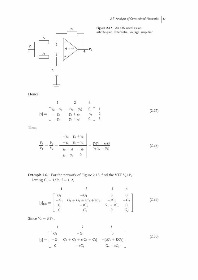
2.7 Analysis of Constrained Networks 27
1
2
34
ya
yc
yd
Vi
yb
VoA → ∞
−
+
Figure 2.17 An OA used as aninfinite-gain differential voltage amplifier.
Hence,
1 2 4
[y] = ya + yc −(ya + yc) 0
−ya ya + yb −yb
−yc yc + yd 0
1
23
(2.27)
Then,
V4
V1= Vo
Vi=
∣∣∣∣∣ −ya ya + yb
−yc yc + yd
∣∣∣∣∣∣∣∣∣∣ ya + yb −yb
yc + yd 0
∣∣∣∣∣= ybyc − yayd
yb(yc + yd)(2.28)
Example 2.6. For the network of Figure 2.18, find the VTF Vo/Vi.Letting Gi = 1/Ri, i = 1, 2,
1 2 3 4
[y]UC =
G1 −G1 0 0−G1 G1 + G2 + sC3 + sC5 −sC3 −G2
0 −sC3 G4 + sC3 00 −G2 0 G2
(2.29)
Since V4 = KV3,
1 2 3
[y] =
G1 −G1 0
−G1 G1 + G2 + s(C3 + C5) −(sC3 + KG2)
0 −sC3 G4 + sC3
(2.30)

28 2 A Review of Network Analysis Techniques
12 3 4K
R1C3
C5 R4
Vo
R2
Vi
Figure 2.18 An OA used as afinite-gain single-input voltageamplifier.
Then,
V3
V1=
∣∣∣∣ −G1 G1 + G2 + s(C3 + C5)0 −sC3
∣∣∣∣∣∣∣∣ G1 + G2 + s(C3 + C5) −(sC3 + KG2)−sC3 G4 + sC3
∣∣∣∣= sG1C3
s2C3C5 + sC3(G1 + G2 + G4 − KG2) + sG4C3 + G4(G1 + G2)(2.31)
Since Vo = V4 = KV3 andV1 = Vi, we get
Vo
Vi= V4
V1= sKG1C3
s2C3C5 + sC3(G1 + G2 + G4 − KG2) + sG4C3 + G4(G1 + G2)(2.32)
2.8Active Building Blocks for Implementing Analog Filters
Several semiconductor building blocks can be used as the active element forimplementing an analog filter. Some examples are (i) OA, (ii) OTA, (iii) CC, and(iv) COA (current operational amplifier) . The OA behaves basically as a VCVS, theOTA as a VCCS, while the CC and COA behave as a CCCS. It is possible to useany of these active devices and several passive-RC components to realize active-RCfilters. If the function of R is simulated by additional active device(s), the entirefilter becomes implementable in a monolithic IC technology.
2.8.1Operational Amplifier
An OA is perhaps the most widely used active device that has been employed toimplement active-RC filter networks. In the ideal form, an OA has infinite inputresistance, zero output resistance, and an infinite voltage gain. The device basicallyworks as a VCVS. In practice, these ideal values are never achieved. But practicaldevices are quite often good enough to produce reasonably accurate transferfunctions. Since a VCVS is a linear network element, the principles of linear

2.8 Active Building Blocks for Implementing Analog Filters 29
A = ∝
1
sC
C
(a) (b)
C
1
(c)
V1
V1
V1
V1
R1 R2 R3
V2 V1 V2
R1 R2
R2
R1
R2
V3
Vo Vo
Vo1
Vo1
Vo = −Rf Vo = −
R1
R1
Rf
R2
R3
V2
V1R1
R2V2
V3
−
+
A = ∝
−
+
A = ∝
−
+
1 + sCR2= −
+ + +
Figure 2.19 An OA used as (a) a summing invert-ing voltage amplifier, (b) a summing inverting inte-grating voltage amplifier, and (c) a lossy invertingintegrating voltage amplifier.
network analysis apply. Using superposition principle one can realize summingamplifiers and summing integrators with an OA and several RC components.Consider Figures 2.19a and 2.19b, which depict a summing amplifier and summingintegrator respectively, realized using ideal OAs.
In the above, the voltages V1, V2, . . . are assumed to be available from voltagesource nodes. Since an OA behaves as a VCVS, the output node of an OA appearslike a voltage source. Thus, any one of the V1, V2 voltages could be derived fromthe output of the OA. When this is done in practice, we say that a feedback(negative) is being applied. Thus, in Figure 2.19b, if we label Vo = Vo1 and makeV2 = Vo1, we get Vo1 = − 1
sCR1V1 − 1
sCR2Vo1, which leads to the transfer function
Vo1V1
= − R2R1
11+sCR2
. This is the transfer function of a lossy integrator circuit as shown
in Figure 2.19c.It may be noted that by providing a feedback, a rational function of s has been
generated. In principle, by combining ideal integrators, lossy integrators, andsumming amplifiers, a frequency-selective transfer function of any high order (>1)

30 2 A Review of Network Analysis Techniques
A = ∝A = ∝
A = ∝
12
3
V1
Vo1Vo2
Vo3
R1
R2
R5
R6
R3
R4
C1C2
−
+
−−
++
Figure 2.20 Use of an OA-based (inverting) integrator and(inverting) amplifier in realizing a second-order active-RCfilter.
can be generated. Consider the case of realizing a second-order filter function asshown in Figure 2.20.
To analyze the system, one can proceed as follows: using nodal equations atnodes 1, 2, and 3, respectively, we get
Vo1 = − V1
sC1R1− Vo1
sC1R2− Vo3
sC1R3, Vo3 = −R6
R5Vo2, and Vo2 = − Vo1
sC2R4
On substitution for Vo3 and Vo2, one finally gets
Vo1
V1= −N(s)
D(s)(2.33)
where
N(s) = R6
R5
s
R1R4C1C2, D(s) = s2 + s
C1R2+ R6
R5
1
R3R4C1C2
The above represents a VTF T(s) = Vo1/V1, of the form As/(s2 + Bs + C). If welet s = jω and use suitable values for the RC elements, the plot of the magnituderesponse in terms of frequency ω rad s−1 will appear like a band-pass filter function.This serves as an example of implementing a band-pass filter using an OA as theactive device.
2.8.2Operational Transconductance Amplifier
The OTA functions as a VCCS, so that the significant transfer characteristic is theoutput short circuit small signal current to input small signal voltage (Schaumann,Ghausi, and Laker, 1990). If the output is terminated in a finite resistance, a VTFcan be easily realized. OTAs can be easily configured to function as a driving pointresistance and thus OTA-based filters may dispense with the use of any lumpedresistances. This opens up the potential for implementing fully monolithic analogfilters. The usual symbol and an associated AC equivalent network for an OTA areshown in Figures 2.21a and 2.21b.

2.8 Active Building Blocks for Implementing Analog Filters 31
++
−−V =V1 −V2
gm gmVI
I
(a) (b)
V1
V2I = gm (V1 −V2)
Figure 2.21 An operational transconductance amplifier(OTA): (a) schematic symbol; (b) AC equivalent circuit ofan ideal OTA.
+_
+
−
−
+
C
V1
Vi
gm11
2
C gm1Vo
gm2V1
gm2
gm3gm3(Vi −Vo)
Vo
Figure 2.22 An OTA-based second-order filter.
Consider Figure 2.22 which presents the schematic of an OTA-based second-orderfilter.
At node 1, sCV1 = −gm1Vo, and at node 2, gm2V1 + gm3(Vi − Vo) = sCVo. Fromthese two relations, we get
Vo
Vi= sgm2C
s2C2 + sgm3C + gm1gm2(2.34)
V1
Vi= −gm1gm2
s2C2 + sgm3C + gm1gm2(2.35)
Vo/Vi represents the VTF of a second-order band-pass filter and V1/Vi that of alow-pass filter. This shows the potential of implementing a filtering function usingOTAs.
2.8.3Current Conveyor
A CC functions as a CCCS and in combination with RC elements can producea frequency-dependent transfer function (Sedra and Smith, 1970). The schematicsymbol of a CC is shown in Figure 2.23, and its input–output relations are given

32 2 A Review of Network Analysis Techniques
CCIIY
X
Z
iX →
iY (= 0) →
← iZ
Figure 2.23 The schematic symbol ofa type 2 current conveyor (CCII).
by
iY
vX
iZ
=
0 0 0
1 0 00 ±1 0
vY
iXvZ
(2.36)
The matrix relations imply that the X,Y terminals act like a virtual short circuit(as is in an OA), while the X, Z terminals function like a current mirror. It ispossible to arrange Iz = ±kIX , where k is a constant. The CC with positive currentmirroring is named as positive current conveyor type 2 (CCII+) and the CCwith negative current mirroring is termed as a negative current conveyor type 2(CCII–). The symbol II represents CC type 2, which has been established as a morepopular and practical device.
If one considers the network with a CCII– of current gain factor k (Figure 2.24),it will be possible to establish by analysis, that a low-pass CTF is realized.
Note that VX = VY = 0. Then KCL at the input node gives
IX = IS + sCV1
At node Z,
IZ = sCV2 + G(V2 − V1) = kIX
where G = (1/R). Substituting for IX and rearranging, we get
(sC + G)V2 − (G + ksC)V1 = kIS (2.37)
At the output node
(V1 − V2)G + V1G + V1sC = 0 (2.38)
X
YZ CCII−
C
C
R
R
V1V2
← IXIZ = kI X↓
↓
Is
Io
Figure 2.24 A negativeCCII-based low-pass currenttransfer function filter.

Practice Problems 33
Equation (2.38) gives
V2 = V1(sC + 2G)/G (2.39)
Substituting for V2 from Eq. (2.39) into Eq. (2.36), we have
V1sC + 2G
G(sC + G) − V1(G + ksC) = kIs (2.40)
Finally, noting that Io = V1G, one arrives at the current-mode transfer function
Io
Is= kG2/C2
s2 + (3 − k)(G/C)s + G2/C2(2.41)
Equation (2.41) represents a second-order low-pass filter transfer function in termsof current signals. The above derivation establishes that a filtering function can beimplemented using a CC device.
Practice Problems
2.1 Consider the ladder network with component values as shown inFigure P2.1. Derive the transfer function for the voltage ratio VL/Vs.
2.2 Find the VTF of the ladder filter shown in Figure P2.2.2.3 Consider the network shown in Figure P2.3 that uses ideal OAs. (a) Find
the chain matrix of the network and show that it corresponds to that of animpedance converter. (b) If a load ZL is connected at port 2, what will be theinput impedance at port 1? (c) If Y1 = Y2 = Y3 = G, Y4 = sC, and ZL = RL
what is the input impedance at port 1?
Vs
RsRL VL
L2 L4
C1C3
+ +
−−
C1 = 0.0114 FL4 = 136 H
Rs = 1RL = 1
C3 = 0.0134 FL2 = 217 H
Figure P2.1
+
− −−+H2
3
F34
H21
1 ΩVs VL+
Figure P2.2

34 2 A Review of Network Analysis Techniques
V1
+
−
I1 →
Y1 Y2
Y3 Y4 ← I21 2
A=
∞A
=∞
+
+
−
−
V2
+
−
Figure P2.3
A = ∞R1 R2
C1
C2
R3
R4
ViVo
+
−
+
−
+
−
Figure P2.4
2.4 Assuming that the OA is ideal, show that the VTF of the active-RC networkof Figure P2.4 is given by
Vo(s)Vi(s)
= K/(C1C2R1R2)
s2 + s
[1
C2R1+ 1
C2R2+ 1
C1R2− K
C1R2
]+ 1
C1C2R1R2
where
K = 1 +(
R4
R3
)
2.5 For the network, shown in Figure P2.5, with a VCVS of gain K, find anexpression for the VTF, V2(s)/V1(s).
2.6 For the network of Figure P2.6, show that the VTF is given by
V2(s)
V1(s)= Ks2
s2 + s
[1
C1R2+ 1
C3R4+ 1
C1R4− K
C1R2
]+ 1
C1C3R2R4

Practice Problems 35
K
V1V2
+
− −
+
R1
R2
R4
C3C5
Figure P2.5
R2
R4
C3C1
K+
−V2
+
−V1
Figure P2.6
If R2 = R4 = 1 , C1 = C3 = 1F, what value of K will make the coefficientof the ‘‘s’’ term in the denominator equal to 1.414?
2.7 The network of Figure P2.7 represents a low-pass filter. Derive the expressionfor the VTF of the network using the method of constrained networks. TheOA is ideal.
2.8 Assuming the OA to be ideal, for the band-pass network shown in FigureP2.8, verify that the VTF is given by
V2(s)V1(s)
= sG1C3
s2C3C4 + sG5(C3 + C4) + G5(G1 + G2)
Note that G1, G2, and G5 are conductances.2.9 Consider the second-order filter network (Ackerberg and Mossberg, 1974)
implemented using three OAs, and shown in Figure P2.9. Assuming thatthe OAs are identical and that each has a finite gain A, show that the VTF,
+
−V1
++
−
−
V2
R1R4
R3
C2
C5
A = ∝
Figure P2.7

36 2 A Review of Network Analysis Techniques
+
−V1
++
−
−
V2
C4C3G1
G2
G1,G2, and G5 are conductances
G5
A = ∝
Figure P2.8
R2
C1
R1
R
Vi+ +
+
+
−
−
−
−
A
A
AVo1
Vo2
r
C2
r1
r2
Figure P2.9
Vo2(s)/Vi(s) is given by
Vo2
Vi
=− 1
rR
1
rR2+
1R
+ 1R2
A+
(1 + 1
A
) (1
R1+ sC1
)
sC2
r1
1
r2+
1r2
+ 1r1
A
+1r
+ sC2
A
2.10 Consider the circuit of Figure P2.10, which is fed from a current source.Each OA has a finite gain A. Show that the current transfer function (CTF),Io/Ii2, is given by

Practice Problems 37
R2
R1
r2
r1
C2C1
+
+
−
−
A
+
−
A
A
R
IoVa
Vb
r
Ii1Ii2
Vo
Figure P2.10
−
−+
+gm1 gm2
−
+
−
+
−
+
gm3
gm4gm5
C1
C2
Vo
VCVBVA
Figure P2.11
Io
Ii2=
− 1
rR
1rR2
+(
1Ar
+(
1 + 1A
)(1
R1+sC1
))
sC2
r1
1r2
+1
r2+ sC2
A
+1
r1+ 1
r2
A
2.11 Using the ideal small signal model for each OTA in Figure P2.11, derivethat
Vo = gm2gm5VA − sgm4C1VB + s2C1C2VC
s2C1C2 + sgm3C1 + gm1gm2
2.12 Figure P2.12 shows a twin-Tee network frequently used in connection withdesign of equalizers. Write a subset of two-port parameters which could beused very easily to derive the overall two-port parameters of the system.

38 2 A Review of Network Analysis Techniques
C1 C2
C3
R2
R3
R1
+
−
+
−V2V1
Figure P2.12
+
+
−
−
+−
gm1
gm2
2
2′
V2
+
−
1
1′
V1
Figure P2.14
R2
I1
1
+
+
+
−
−
−
V1
V2
R1
I2 2
2′
1′
Figure P2.16

Practice Problems 39
Using the overall two-port parameters of the system, derive an expressionfor the voltage transfer function V2/V1.
2.13 Solve Problem 2.12 using the method of indefinite admittance matrix (IAM).2.14 (a) Derive the chain matrix [a] for the circuit of Figure P2.14, which employs
two OTAs. Show that it corresponds to a PII. (b) Show that the driving pointimpedance Z1 = V1/I1 is given by YL/gm1gm2, where ZL is the load connectedat port 2. (c) If ZL corresponds to that of a capacitor C, find the equivalentelement seen at port 1 and its value.
2.15 Suggest a circuit for an NII using OTAs. Use the knowledge you have gainedfrom solving Problem 2.14.
2.16 Show that the circuit of Figure P2.16 realizes a CNIC. What is the inputimpedance at port 1, if a load ZL is connected at port 2?
2.17 Show that the forward VTF Vo2(s)/Vi(s) of Problem 2.9 is the same as thereverse CTF Io/Ii2 of Problem 2.10, when the OAs are ideal. Observe thatthe two circuits are the same except that the input and output terminals ofeach of the OAs are interchanged in the two circuits.

41
3Network Theorems and Approximation of Filter Functions
In the previous chapter, we considered different methods of analyzing electricalcircuits containing passive and active elements, and discussed various ways ofcharacterizing a two-port network, which is extremely useful in understanding filterdesign. In this chapter, we introduce some general network theorems that are usefulin filter design. This is followed by magnitude and phase approximations for thesynthesis of the filter function. The ideal frequency response characteristic of a filterassumes brick-wall characteristics with abrupt jumps at the transition between thepassbands (PBs) and stopbands (SBs). In reality, such a response is not achievable.Instead, filter designers contend themselves by attempting to approximate theidealized characteristics with some special mathematical functions, which veryclosely match the ideal brick-wall characteristics. By doing so, some of the idealnessis sacrificed, but the approximation functions lead to the realization of filters usingreal components. This part of the filter design is known as the task of approximation.For magnitude approximation, the cases of maximally flat, Chebyshev (CHEB), andelliptic functions are discussed. For phase approximation, Bessel–Thomson (BT)approximation is introduced.
3.1Impedance Scaling
Consider a linear time-invariant (LTI) n-port network N. Let N contain one-portelements as well as two-port elements. This has been assumed for the sake ofsimplicity, but the results to be established are true even if the subnetworks aren-port networks. From Chapter 2, we know that we can write the IAM of the n-port as
[I] = [Y ]N [V ] (3.1)
Let us multiply all the one-port impedances and the impedance matrices of theinternal two-ports by a constant positive value k. It is clear that as a consequence,all the one-port admittances as well as the [y] matrices of the internal two-ports aremultiplied by (1/k). Hence, Eq. (3.1) becomes
[I] = (1/k)[Y ]N [V ] (3.2)
Modern Analog Filter Analysis and Design: A Practical Approach. Rabin Raut and M. N. S. SwamyCopyright 2010 WILEY-VCH Verlag GmbH & Co. KGaA, WeinheimISBN: 978-3-527-40766-8

42 3 Network Theorems and Approximation of Filter Functions
It is seen from Eqs. (2.20) and (2.21) that the DPI between the nodes q and l alsoget multiplied by the same factor k, whereas the VTF between the node pairs (i, j)and (q, l) is unaltered. This process is known as impedance scaling. It is very clearthat impedance scaling by a factor of k is equivalent to changing a resistor of valueR to kR, an inductor of value L to another inductor of value kL, and a capacitorof value C to another capacitor of value C/k. We will see what happens to varioustypes of internal two-ports a little later.
3.2Impedance Transformation
By applying the same arguments as above, it is obvious that if we multiply all theinternal one-port impedances as well as the two-port [z] matrices by a functionf(s), then the DPIs between any two nodes k and l will also be multiplied by f(s),while the VTF between the pairs (i, j) and (k, l) will be unaffected. We shall call theoperation of multiplying the internal impedances or impedance matrices by f(s) asimpedance transformation by f(s) (Swamy, 1975). Since most of the time we will bedealing with two-port networks, let us assume that we are dealing with a two-port,which consists of one-ports and two-ports as subnetworks. Let its chain matrix bedenoted by[
V1
I1
]=
[A BC D
] [V2
−I2
](3.3)
It is clear that as a consequence of the impedance transformation, an internalresistor or inductor gets multiplied by f(s), while the capacitor gets divided by f(s).Let us see what happens to an internal two-port, which is represented by its chainmatrix as[
aj] =
[Aj Bj
Cj Dj
](3.4)
where Aj, Bj, Cj, and Dj are, in general, functions of s. In view of the interre-lationships between the chain and [z] matrices of two-ports, the consequence ofthe impedance transformation is to render the chain matrix of the transformednetwork to be
[a′] =[
A Bf (s)C/f (s) D
](3.5)
while the chain matrix of the internal two-port becomes[a′
j
]=
[Aj Bjf (s)
Cj/f (s) Dj
](3.6)
Thus, if the network consists of VCVS or CCCS, these elements will remainas VCVS or CCCS with the same voltage or current amplification factor underimpedance transformation. Using Eq. (3.6), we may similarly find the transformedelements for the other two-port elements listed in Table 2.1.

3.2 Impedance Transformation 43
K = 2.9
R1 = 1 Ω R2 = 1 Ω
C1 = 2 F
C2 = 2 F
K+
− −V1 V2
+
Figure 3.1 An active-RC filterusing one OA.
Let us see what has been the effect on the overall two-port of impedancetransformation by f(s) (or scaling by a factor k). We can conclude the followingusing Eq. (3.5):
1) Driving point and transfer impedances are multiplied by f(s).2) Driving point and transfer admittances are multiplied by 1/f(s).3) The open circuit VTF (1/A) is unaltered.4) The short circuit CTF (1/D) is unaltered.
Example 3.1. Figure 3.1 shows an active-RC filter using one OA. Determine thetransfer function (TF) V2/V1 and hence the nature of the filter. Determine thevalue of the element if R1 is chosen as (scaled to) R1 = 1 k. Also find the new TF.
It can readily be seen that
Tv = V2
V1= K/C1C2R1R2
s2 + s[
1C1
(1
R1+ 1
R2
)+ (1 − K)/C2R2
]+ 1
C1C2R1R2
Since C1 = C2 = 2 F, R1 = R2 = 1 , and K = 2.9
V2
V1= Tv = 2.9/4
s2 + 0.05s + 0.25
Hence, the given network is a low-pass (LP) filter. If now R1 is scaled to 1 k, theimpedances are all scaled by 1000, but not K. Hence, the capacitive impedancesare multiplied by 1000. In other words, the capacitor values are divided by 1000.Hence, the new element values are
R1 = R2 = 1 k , C1 = C2 = 2 MF, K = 2.9
Also since the voltage TF is unaltered by impedance scaling, the value of the newTF is still the same as before.
Example 3.2. Figure 3.2 shows a normalized filter working into a 1 loadresistance. Obtain the system function V2/I1. Find the filter corresponding to a100 load resistance. Find the new system function.

44 3 Network Theorems and Approximation of Filter Functions
I1
C1 = 1 F C3 = 1 F
1 Ω
L2 = 1 H +
V2
−
Figure 3.2 An LC filter with a normalized load resistance of 1 .
1/100 FI1
2000 H
1/100 F
V2
100 Ω
+
−
Figure 3.3 The LC filter corresponding to that of Figure 3.2 for a load of 100 .
The system function given by V2/I1 = Z21 is
Z21 = 1
s3C1L2C3 + s2L2C1 + s (C1 + C3) + 1= 1
2s3 + 2s2 + 2s + 1
To obtain the filter corresponding to a 100 resistance at the load we perform thefollowing scaling:
R∗i = 100Ri = 100 , L∗
2 = 100L2 = 200 H, C∗1 = C∗
2 = 1
100F
Hence,
Z∗21 = 100Z21 = 100
2s3 + 2s2 + 2s + 1
The scaled circuit is shown in Figure 3.3.
3.3Dual and Inverse Networks
3.3.1Dual and Inverse One-Port Networks
It is well known that if two one-port RLC networks N1 and N2 have their impedancesz1 and z2 related by
z1z2 = K (3.7)

3.3 Dual and Inverse Networks 45
then N1 and N2 are said to be inverses of each other with respect to K. If thenetwork N1 is a planar one-port network, it is also known that we can obtain N2 byobtaining the topological dual of N1 by the ‘‘dot window’’ technique (Swamy andThulasiraman, 1981) and associating an impedance of ziD to the ith branch of N2
such that
ziziD = K (3.8a)
or
ziD = Kyi (3.8b)
where zi is the impedance of the corresponding ith branch in N1. It may be notedthat the unit of K is ohms square. When N2 is obtained from N1 in this way, N2
is known as the dual of N1 w.r.t. K. (If K = 1, the two networks are simply knownas duals of each other). Hence, a resistor R in N1 would become a resistor of valueK/R1 in N2, an inductor of value L would become a capacitor of value L/K in N2
and a capacitor C in N1 would become an inductor of value KC in N2.If K = f (s), a function of s, then we call N2 the generalized dual of N1 w.r.t. f (s)
(Mitra, 1969). N1 is not restricted to be an RLC network. Of course, the individualelements in the two networks are also correspondingly generalized duals of eachother w.r.t. f (s). When f (s) = K/s, the network N2 is called the capacitive dual of N1
and is useful in RC-active synthesis where we would like to obtain one RC-activenetwork from another (an ordinary resistive dual, f (s) = K, would convert an RCnetwork to an RL network). In this book, we do not make a distinction betweenduals and inverses, and simply call them as duals, even if we do not obtain theduals topologically.
3.3.2Dual Two-Port Networks
It is possible to extend the generalized dual concept for a planar two-port networkconsisting of one-ports and three-terminal two-ports as internal elements, whereinthe dual is topologically obtained from the original two-port (Swamy, Bhusan, andBhattacharyya, 1974). However, it is not done so here, but the generalized dual orgeneralized inverse is defined through the two-port chain matrix (Swamy, 1975).Let N be an LTI 2-port network with a chain matrix
[a] =[
A BC D
](3.9)
We define ND to be the generalized dual (or generalized inverse) of N w.r.t. f (s) ifthe chain matrix [a]D of ND is related to [a] as
[a]D =[
D Cf (s)B/f (s) A
](3.10)
As in the case of one-ports, if f (s) = 1/s, we call the dual as the capacitive dual. It isobvious that the dual of the dual is the original network. Now, using Table 2.1, we

46 3 Network Theorems and Approximation of Filter Functions
can show that
[z]D = f (s)[
y11 −y12
−y21 y22
](3.11)
Hence, the VTF and CTF are given by
Tv(s) = V2
V1= − y21
y22= (z21)D/f (s)
(z22)D/f (s)= (z21)D
(z21)D= (TI)D (3.12)
TI(s) = −I2
I1− y21
y11= (z21)D/f (s)
(z11)D/f (s)= (z21)D
(z11)D= (TV )D (3.13)
Thus, we have the following properties:
1) The open circuit voltage TF TV of N is the same as the short circuit current TF(TI)D of ND and vice versa, that is,
TV = (TI)D , (TV)D = TI (3.14)
2) The DPIs z11 and z22 of N are f (s) times the driving point admittances y11 andy22, respectively, of ND and vice versa, that is,
(z11)D = f (s)y11, (z22)D = f (s)y22; z11 = f (s)(y11
)D ,
z22 = f (s)(y22
)D
(3.15)
3) The transfer impedances z12 and z21 of N are −f (s) times the transfer admit-tances y12 and y21, respectively, of ND and vice versa, that is,
(z12)D = −f (s)y12, (z21)D = −f (s)y21; z12 = −f (s)(y12
)D ,
z21 = −f (s)(y21
)D (3.16)
The property (1) above is particularly useful in obtaining a CTF realization from aknown VTF realization. Using the definition of the generalized dual, the followingresults can easily be established.
Theorem 3.1. The generalized dual of a cascade of networks w.r.t. f (s) is the cascade ofthe generalized duals w.r.t. f (s), that is,[
N1 N2 · · · Nm]
D= [N1]D [N2]D · · · [Nm]D (3.17)
Theorem 3.2. The generalized dual ZD of a series (shunt) element of impedance Z isa shunt (series) element of impedance f(s)/Z. Thus, Z ZD = f(s), that is, the one-portsZ and ZD are themselves generalized duals of each other. Figure 3.4 illustrates theseoperations.
Example 3.3. Obtain the capacitive dual of the RC ladder structure shown inFigure 3.5a.

3.4 Reversed Networks 47
Y
z
Dual
Dual
zD = f (s) /z
f (s)YYD
1=
Figure 3.4 Series and shunt elements and their generalized duals.
V1 V2
R1 R2 Rn
C1 C2 Cn
(a)
(b)
+
−
+
−
C1 C2 l2CnI1
R1 R2 Rn
Figure 3.5 (a) An RC laddernetwork and (b) its capacitivedual.
Using the results of Theorems 3.1 and 3.2, it is easily seen that the capacitivedual is another RC ladder as shown in Figure 3.5b. It may be verified that the opencircuit VTF of the RC ladder (Figure 3.5a) is the same as the short circuit CTF ofthe RC ladder of Figure 3.5b.
3.4Reversed Networks
Consider a two-port network N whose [z] matrix is given by
[z] =[
z11 z12
z21 z22
](3.18)
The reversed network NR is obtained by reversing the roles of the input and outputsin N. Hence, the z matrix of the reversed network is
[zR] =[
z22 z21
z12 z11
]
Hence, from Table 2.1, we have that the chain matrix of the reversed network is
[aR] = 1
AD − BC
[D BC A
](3.19)
If the network is reciprocal, AD − BC = 1.

48 3 Network Theorems and Approximation of Filter Functions
3.5Transposed Network
Consider a two-port network N with its impedance matrix given by [z]. Bhattacharyyaand Swamy (1971) defined the two-port network having an impedance matrix thatis the transpose of [z] as the transposed network (Bhattacharyya and Swamy, 1971),or simply the transpose of N, and denoted it by NT. Denoting the impedance andadmittance matrices of NT by
[zT
]and
[yT
], we thus have
[zT
] = [z]T and[yT
] =[y]T . Correspondingly, the chain matrix
[aT
]of NT is related to the chain matrix [a]
of N by
[aT
] = 1AD − BC
[a] (3.20)
This definition could be of course extended to n-ports (Bhattacharyya and Swamy,1971). It is clear that for a reciprocal network, since z12 = z21, the transposeis itself. It can be shown that if the network N consists of one- and two-portelements, the transposed network NT can be obtained from N by replacing theinternal nonreciprocal two-ports by their transposes and leaving the one-ports andreciprocal two-ports unaltered (Bhattacharyya and Swamy, 1971).
If we now denote the reversed transpose of N by (NT)R, then the chain matrix of(NT)R is given by
[aT
R
] =[
D BC A
](3.21)
We can use the above relation to determine the transposes of the various nonre-ciprocal two-ports. The reversed transposes of the various nonreciprocal two-ports(including the controlled sources) are listed in Table 3.1.
From Table 3.1, we observe that the transpose of a VCVS is a CCCS with itsinput and output ports reversed and with a current gain equal to the voltage gainof the VCVS, and vice versa. Also, the transpose of an impedance inverter, aVCCS or a CCVS, is itself with input and output ports reversed. Thus, we can veryeasily construct the transpose of a given network with one-ports and two-ports assubnetworks using Table 3.1.
From the above analysis, the following important conclusions can be drawn:
1) The driving point functions of NT are the same as those of N.2) The forward open circuit VTF of a network N is the same as the reverse short
circuit CTF of its transpose NT , and vice versa.3) The forward transfer impedance (admittance) of N is the same as the reverse
transfer impedance (admittance) of NT , and vice versa.
It should be noted again that if N is reciprocal, NTR is nothing but NR, the reversed
network of N. Thus given a network N, we can obtain three other networks,namely, the dual ND, the reversed transpose NT
R , and N = (NT
R
)D = (ND)T
R. Theinterrelationships between these four networks are pictorially shown in Figure 3.6along with their chain matrices (Swamy, Bhusan, and Bhattacharyya, 1976).

3.5 Transposed Network 49
Table 3.1 Reversed transposes of some of the common two-port elements.
Two-portelement N
[a] Chain matrix of N [aTR] Chain
matrix of NTR
Reversed transpose of elementN
VCVS
[1µ
0
0 0
]
µ = voltage gain
[0 00 1
µ
]CCCS of gain µ
CCCS
[0 00 1
α
]α = current gain
[ 1α
00 0
]VCVS of gain α
VCCS
[0 1
g
0 0
]
g = transconductance
[0 1
g
0 0
]VCCS of transconductance g
CCVS[
0 01r 0
]r = transresistance
[0 01r 0
]CCVS of transresistance r
Impedanceconverter
[K1 00 K2
] [K2 00 K1
]Another impedance converter
Impedanceinverter (II)
[0 1
G1G2 0
] [0 1
G1G2 0
]Same impedance inverter as N
Reversed transposed
Reversed transposed
Gen
eral
ized
dua
l
Gen
eral
ized
dua
l
DC
BA
AC
BD
= Af (s)
Cf (s)BD
N NTR
NDN =
=a
D
TR= (ND)
aD
=A
f (s)
Cf (s)BD
a
aRT =
NRT
Figure 3.6 Interrelationships among N, ND, NTR , and N = (
NTR
)D = (ND)T
R .
As a consequence, we see that
1) The open circuit VTFs (short circuit CTFs) of N and N are identical. Hence, Nand N are alternate structures for a VTF or a CTF.
2) The open circuit VTFs (short circuit CTFs) of ND and NTR are identical.
3) The open circuit VTF (CTF) of N and N is the same as the CTF (VTF) of ND
and NTR .

50 3 Network Theorems and Approximation of Filter Functions
4) The DPIs of N and NT are the same.5) The DPIs of ND and NT
R are the same.
3.6Applications to Terminated Networks
Lossless networks terminated by resistors, either at one end or at both ends, are usedin communication systems to couple an energy source to a load. The design of loss-less ladder networks is considered in detail in any text book on passive network syn-thesis (see, for example, Van Valkenburg, 1960; Weinberg, 1962). It has been shown(Temes and Mitra, 1973) that when the ladder is designed properly, the first-ordersensitivities of the magnitude of the TF to each of the inductors and capacitors arezero at the frequencies of maximum power transfer, and further that they remainlow in the intermediate frequencies throughout the PB. In this section, we considerthe applications of dual, transposed, and dual-transposed networks in doubly ter-minated networks. Similar results can be obtained for singly terminated networks.
A general coupling network may be excited by a voltage source or a currentsource, which may be nonideal. Further, the network may be working into anarbitrary load. Such a situation can be represented by the network of Figure 3.7a orb, and is known as a doubly terminated network.
For the network of Figure 3.7a, the suitable specifications are
TV (s) = V2
Vs= RL
ARL + B + CRsRL + DRs(3.22)
and
Y21(s) = −I2
Vs= 1
ARL + B + CRsRL + DRs(3.23)
while for the network of Figure 3.7b, the suitable specifications are
TI(s) = − I2
Is= Rs
ARL + B + CRsRL + DRs(3.24)
and
Z21(s) = V2
Is= RsRL
ARL + B + CRsRL + DRs(3.25)
Thus, if we know how to realize a rational function H(s), say, as the TV (s) of adoubly terminated network with a load resistance RL and source resistance RS, then
Rs
RLISV2 Rs RL
I1 I2 I1 I2
NVS N
+
−
V2
+
−
(a) (b)
Figure 3.7 Doubly terminated networks fed by (a) a voltage source and (b) a currentsource.

3.6 Applications to Terminated Networks 51
A B
C D
R
1
A
B
C
D
1
R
N
+
−VS
+
−
V2
+
−VS
+
−
V2
+
−V2
+
−V2
+
−VS
+
−VS
D CR
B/R A
1
R
A
D
R
1
B/R
CR
NDN = NT
RD
(a) (b)
(c) (d)
RTN
Figure 3.8 Doubly terminated networks (a) N, (b) ND, (c) NTR , and (d) N = (ND)T
R .
the designs for TI(s), Y21(s), and Z21(s) are directly obtained. Equations (3.22–3.25)may also be used in the case of singly terminated networks.
Let us denote RSRL by R and assume without loss of generality that RL = 1, sincewe can always scale the impedances for any other load resistance. Consider thenetworks of Figures 3.8a–3.8d, where ND is the dual of N w.r.t. f (s) = R, NT
R isthe reversed transpose of N, and N = (ND)T
R. The TF of these structures may beobtained using Eqs. (3.22–3.25) as
T(a)V (s) = 1
RT(b)
V (s) = 1R
T(c)V (s) = T(d)
V (s) = H(s) (3.26)
where
H(s) = 1
(A + B) + R (C + D)(3.27)
Thus, if we know how to synthesize a given H(s) as the TV (s) of the structure ofFigure 3.8a and obtain the two-port N, then three other realizations may be foundfor H(s) using ND, NT
R , and N. It should be noted, however, that the source andload conditions are the same for Figures 3.8a and 3.8d, and again for Figures 3.8band3.8c. Further, source and load resistances for the former networks are the loadand source resistances for the latter. Hence (Swamy, 1975),
1) Figures 3.8a and 3.8d show alternate structures realizing H(s) as a voltage TFwith a load of 1 and a source of R, and one may be obtained from theother.
2) Figures 3.8b and 3.8c show alternate structures, but have a load of R and asource of 1 ; further these structures may be directly obtained from that ofFigure 3.8a.

52 3 Network Theorems and Approximation of Filter Functions
3.7Frequency Scaling
Consider a general LTI network N. If we change the complex frequency s to s/b, bbeing a constant, it is clear that in any of the system functions, whether it be the TIFZ21(s), the TAF Y21(s), the VTF TV (s), or the CTF TI(s), the frequency s is changedto s/b. Hence, whatever was the magnitude or phase of a system function F(s) at afrequency ω, the new system function F(s/b) would have the same magnitude andphase at the frequency ω/b, that is, the frequency has been scaled by a factor 1/b.Such an operation is called frequency scaling by the factor 1/b. As a consequence ofthe frequency scaling, it is clear that an inductance of value L and a capacitor of valueC would now have reactances of sL/b and 1/(sC/b), respectively. Thus, these willbecome, respectively, an inductor of value L/b and a capacitor of value C/b, whilea resistor will remain unchanged. It is also seen that the ideal controlled sourcesalso remain unaltered. Frequency scaling is used to obtain the response of a givenfilter in a given frequency band scaled up or down to a different frequency band.
Example 3.4. The Sallen and Key structure of Figure 3.1 realizes the LP TF
V2
V1= TV (s) = 2.9/4
s2 + 0.05s + 0.25
According to the standard notations for a second-order filter, namely,
TV (s)∣∣LP = HLP 2
p
s2 + (ωp/Qp)s + ω2p
the above filter has a pole frequency ωp = √0.25 = 0.5.
(a) Find the TF if ωp is to be 1000 rad s−1.(b) If in addition, we want to use 1 K resistors in the circuit, how is the TF altered.
Also, how do the values of the components change in the LP structure?Solution: (a) The frequency scaling factor is b = 1000/0.5 = 2000. Hence, s is
changed to s/2000 in the expression for TV (s), giving the new TF to be
T ′V (s) = (2.9/4)(2000)2
s2 + 0.05(2000)s + 0.25(2000)2
This does not alter the values of the resistors, but the capacitance values become0.001.
(b) If all the resistors have to be 1 K, we have to scale all the impedancesby the factor a = 1000. Since impedance scaling does not alter a VTF, the TFremains T ′
V (s). However, the new values of the components are R1 = R2 = 1000
and C1 = C2 = 1 pF, with the gain K = 2.9 of the voltage amplifier remainingunchanged.
3.8Types of Filters
Filters are categorized depending on the type of filtering function that they perform.If the primary consideration is the magnitude or attenuation characteristic, then

3.8 Types of Filters 53
we classify them as LP, high-pass (HP), band-pass (BP), and bandstop (BS) orband-reject (BR). However, if our main concern is the phase or delay specification,then the type of filters are all-pass (AP) and delay equalizers. In all these cases, theTF to be realized is of the form
H(s) = N(s)
D(s)= k
sm + · · · + a1s + a0
sn + · · · + b1s + b0, m ≤ n (3.28)
An LP filter is to pass low frequencies from DC to a desired frequency ωc, calledthe cutoff frequency, and to attenuate frequencies beyond the cutoff. An ideal LPfilter would have a magnitude for H
(jω
)that is constant from zero to ωc and zero
beyond ωc. The frequency band from DC to ωc is called the passband. However,such a brick-wall characteristic is impossible to realize in practice, and the LP filterspecifications are always given in terms of its cutoff frequency ωc, an SB frequencyωs, maximum loss (Ap) allowed in the PB, and minimum SB attenuation (As). The
20 log10
SB
H ( jw)
H ( j 0)
PB
TB
SBPB
TB
Ap Ap
Ap
Ap Ap
AS
≥ ASAS
AS
AS
PB
TB
TB
SBPB
TB
SB
TB
SB PB
dB
H ( jw) dB
H ( jw) dB
H ( jw) dB
wcw→
ws
ws1 ws2w→
wc1 wc2
wc1 wc2
w→
ws1 ws2
wcw→
ws(a)
(c)
(d)
(b)
Figure 3.9 Typical specifications of (a) an LP filter,(b) an HP filter, (c) a BP filter, and (d) a BR filter.

54 3 Network Theorems and Approximation of Filter Functions
frequency range from ωc to ωs is termed the transition band (TB) (see Figure 3.9a). Anideal HP filter passes all frequencies beyond the cutoff frequency ωc and attenuatesall frequencies below it. However, a practical HP filter is characterized in a waysimilar to the LP filter in terms of an SB frequency and a maximum PB loss (seeFigure 3.9b). A BP filter passes a finite band of frequencies bounded by two cutofffrequencies ωc1 and ωc2, and attenuates all frequencies below ωc1 and those aboveωc2. The attenuations in the two SBs may be different, as well as the widths of the twoTBs (see Figure 3.9c). A BR filter attenuates a finite band of frequencies boundedby two cutoff frequencies ωc1 and ωc2, and passes all frequencies below ωc1 andthose above ωc2. Thus, a BR filter has two PBs and the attenuations in the two PBsmay be different; also the widths of the two TBs may be different (see Figure 3.9d).
Sometimes we need a filter which has a null at a particular frequency; such filtersare called null or notch filters. Apart from these filters, we also have gain equalizersthat are used to shape the gain versus frequency spectrum of a given signal. Foraudio signal processing, phase is not as important as the magnitude of the TF.However, it is very important in the case of video signal processing. The phasedistortion causes a variable delay. In such a case, an AP filter is used for phasecorrection or to provide delay equalization. An AP is one for which the magnitudeof the TF is constant, whereas its phase is a function of frequency.
3.9Magnitude Approximation
The specifications for a filter, whether it be a LP, HP, BP, or BR, are given interms of the PB, TB, and SB regions as well as in terms of the loss requirementsin the PB and the SB. The magnitude approximation problem consists of findinga suitable magnitude function, whose magnitude characteristics satisfy the givenspecifications, and which is realizable in practice. We first consider the approxima-tion problem for a LP filter, and then introduce frequency transformations so thatwe can design HP, symmetrical BP, or BR filters for a given set of specifications.For an LP filter, these specifications are usually given in terms of (i) the maximumloss in the PB, Ap, in decibels (dB), (ii) the PB edge (i.e., cutoff ) frequency, ωc, inradians per second (rad s−1), (iii) the loss in the SB, As, in decibels, and (iv) the SBedge frequency, ωs, where the loss is at least As decibels, as shown in Figure 3.9.Without loss of generality, we assume that the cutoff frequency for the LP filter is 1rad s−1, since we can always employ frequency scaling to convert it to an LP filter ofany given cutoff frequency. Such an LP filter is called the normalized LP filter, andwe shall denote the magnitude response of such a normalized filter by
∣∣HN(
jω)∣∣.
In the ideal case,∣∣HN
(jω
)∣∣ = 1 in the PB (0 ≤ ω ≤ 1) and zero in the SB (ω > 1).One can define the characteristic function K(s) of the filter to be such that∣∣K( jω)
∣∣2 = 1∣∣HN ( jω)∣∣2 − 1 (3.29)
Thus,∣∣K( jω)
∣∣2 → 0 in the PB and∣∣K( jω)
∣∣2 → ∞ in the SB. The magnitude
approximation principle assumes that∣∣K( jω)
∣∣2remain less than or equal to ε2 in

3.9 Magnitude Approximation 55
the PB, where ε is a small number. Similarly in the SB,∣∣K( jω)
∣∣2approximates to a
value greater than or equal to δ2, where δ is a very large number. In the PB, the lossAp in decibels is related to the number ε as follows:
Ap = 10 log1∣∣HN( jω)
∣∣2
so that
ε2 = ∣∣K( jω)∣∣2 = 1∣∣HN ( jω)
∣∣2 − 1 = 100.1Ap − 1
Hence,
ε =√
100.1Ap − 1 (3.30)
By similar reasoning, we arrive at
δ =√
100.1As − 1 (3.31)
It must be noted that now onwards ω is the normalized angular frequency,normalized w.r.t. ωc. Similarly, ωs is the normalized SB edge frequency, i.e.,ωs = ωa/ωc, where ωa is the given SB edge frequency
3.9.1Maximally Flat Magnitude (MFM) Approximation
Assuming the function K(s) to be
K(s) = εsn (3.32)
we get from Eq. (3.29)∣∣Hn( jω)∣∣ = 1√
1 + ε2 ω2n(3.33)
Expanding the RHS of the above expression, we have∣∣Hn( jω)∣∣ = 1 − ε2 1
2ω2n + ε4 3
8ω4n − ε6 5
16ω6n + · · · (3.34)
It is clear from Eq. (3.34) that the first (n − 1) derivatives of∣∣Hn( jω)
∣∣ are zero at ω
= 0 (i.e., at DC), and further that∣∣Hn(0)
∣∣ = 1 from Eq. (3.33). Thus, the slope is asflat as can be made since K(s) was chosen as the nth-order polynomial. This is whyEq. (3.33) is called maximally flat magnitude (MFM) approximation for the LP filter.
At the edge of the PB, the frequency is ωc = 1, and ε2 = ( 100.1Ap − 1). Also, atthe SB frequency ωs, ( 100.1As − 1) = ε2 ω2n
s . Hence, the minimum order of theMFM filter necessary to meet the specifications is given by
n = log η
2 log ωs(3.35a)
where
η = 100.1As − 1
100.1Ap − 1(3.35b)
If n is not an integer, the next higher integer value is chosen.

56 3 Network Theorems and Approximation of Filter Functions
One of the important special cases of the MFM approximation is the Butterworthapproximation, which is obtained by choosing ε = 1. It is seen in this case that atthe PB edge, the magnitude of the Butterworth filter is always 0.707, that is, 3 dBdown from its DC (ω = 0) value, irrespective of the order of the filter.
3.9.1.1 MFM Filter Transfer FunctionIt is clear from Eq. (3.33) that the TF HN (s) will be an all-pole function. Assumingthe denominator of HN (s) to be D(s), we have∣∣HN (s)
∣∣2 = 1
D(s)D(−s)(3.36)
Since the poles of HN (s) have to be in the left half (LH) of the s-plane for stability,we associate the LH plane poles to HN (s) and the right-half ones to HN (−s). Nowextending the MFM approximation given by Eq. (3.33) to the s-domain, we get∣∣HN (s)
∣∣2 = 1
1 + ε2(−s2)n(3.37)
Hence, we associate the LH plane roots of
1 + ε2(−s2)n = 0 or ε2ns2n = (−1)n+1 (3.38)
with the poles of D(s). The roots of Eq. (3.38) are complex and are given by
sk = ε−1n exp
(j2k + n − 1
2nπ
)k = 1, 2, . . . , 2n (3.39)
where we have used the fact that exp( jπ ) = −1. These roots are all uniformly
located on a circle of radius ε−1n ; hence, for a Butterworth filter approximation, they
are all uniformly located on the unit circle. Denoting the poles of the MFM filter bypk, and associating the LH plane roots of Eq. (3.39) with pk, we get the poles to be
pk = ε−1n exp
(j2k + n − 1
2nπ
)k = 1, 2, . . . , n (3.40)
The denominator D(s) of the normalized MFM filter is given by
D(s) =∏
k
(s − pk) (3.41)
For Butterworth filters, the polynomial D(s) for various values of n is tabulated inAppendix A, and these polynomials are called Butterworth polynomials.
Example 3.5. Derive the TF for an MFM filter with a PB loss of 3 dB at 10 kHz andan attenuation of at least 100 dB at f ≥ 100 kHz.
It is clear that Ap = 3 dB, As = 100 dB, ωc = 2π × 104 rad s−1, and ωs = 2π ×105 rad s−1. Using these values in Eq. (3.35) we obtain the order of the filter asn = 5. Since the PB loss is 3 dB, it is obvious that it corresponds to a Butterworthfilter. Hence, we can use Appendix A to obtain the Butterworth polynomial ofdegree 5, which will be the denominator of the normalized Butterworth filter oforder 5. Thus, the normalized TF is
HN (s) = 1(s + 1)(s2 + 0.618s + 1)(s2 + 1.618s + 1)
(3.42)

3.9 Magnitude Approximation 57
0
−50
−10010−1
−1
−2
−3
−4
−5
−6
100 101
0
0 2000 4000 6000 8000 10000 12000
0
−20
−40
−60
−80
−100
−1200 2 4 6 8 10 12
× 104
(a)
(b)
(c)
H(s
)dB
→H
(jw
)dB
→
f (Hz)→
f (Hz)→
Figure 3.10 Magnitude response of (a) Butterworthfifth-order normalized LP filter. (b) Response of thedesired filter around the PB edge. (c) The overallresponse of the desired filter.

58 3 Network Theorems and Approximation of Filter Functions
The next task is to derive the frequency-denormalized filter TF H(s) by frequencyscaling:
H(s) = HN
(s
ωc
)
=9.7967 × 10²³
[(s + 6.2842 × 10⁴)(s2 + 3.8835 × 10⁴ s + 3.9488 × 10⁹)×(s2 + 1.0166 × 10⁵s + 3.9488 × 10⁹)]
The response of the normalized filter as well as that of the required Butterworthfilter, obtained using MATLAB program, is depicted in Figures 3.10a–3.10c, andthe MATLAB program for the magnitude response of the normalized filter isprovided in Program 3.1, while that for the denormalized filter is provided inProgram 3.2.
Program 3.1 MATLAB code for the normalized Butterworth filter of Example 3.5
%MATLAB program listing for HN(s), 5th order Butterworth Filterw=logspace(-1,1);s=0+w*i;b=[0,0,0,0,0,1];a=[1,3.2361,5.2361,5.2361,3.2361,1];h=freqs(b,a,w);amag=abs(h);y=20*log(amag);subplot(2,1,1),semilogx(w,y);end
Program 3.2 MATLAB code for the denormalized Butterworth filter of Example 3.5
%MATLAB program listing for |H(s)|, 5th order ButterworthFilterpi=3.14159;fc=1E4;fs=1E5;n=2*pi*fc;% to be used for frequency scaling factorb6=n^5;a1=1.0;a2=3.2361*n;a3=5.2361*n^2;a4=5.2361*n^3;a5=3.2361*n^4;a6=b6;b=[0,0,0,0,0,b6];a=[a1,a2,a3,a4,a5,a6];r1=1.1;r2=1.1*(fs/fc);np=100; % number of points in the graphdf=(r1*fc)/np;% this will show response up to 1.1 times thepassband% edge frequencydf=(r2*fc)/np;% this will show re-sponse up to 11.1 times the passband% edge frequency, i.e., beyond the given stopband edgefrequencyfor n=1:(np+1)w=(n-1)*2*pi*df;s=0+w*i;anum=b6;denm=a1*s^5+a2*s^4+a3*s^3+a4*s^2+a5*s+a6;

3.9 Magnitude Approximation 59
tfs=anum/denm;amag=abs(tfs);y(n)=20*log10(amag);f=w/(2*pi);x(n)=f;end;plot(x,y)gridend
Example 3.6. Repeat the previous problem, but for a PB loss of only 1 dB, with allthe other specifications remaining the same.
Using Eq. (3.35) for n, one finds n = 5.29. Hence, we choose n = 6. Furtherfor Ap = 1 dB, ε = 0.50885. Thus, ε−1/n = 1.11918. An examination of Eq. (3.40)shows that the poles of the MFM filter for a given n for any value of ε are thesame as those of the Butterworth filter of order n, except that they are multipliedby ε−1/n. We shall first use the table of Butterworth functions for n = 6 to obtainthe denominator polynomial as
DB(s) = s6 + 3.8637s5 + 7.4641s4 + 9.1416s3 + 7.4641s2 + 3.8637s + 1
(3.43)In order to get the D(s) for Ap = 1 dB, we substitute ε1/ns = 0.8935s in place of sin DB(s) given by Eq. (3.43). Hence, the denominator polynomial for the requiredMFM filter is given by
D(s) = DB(0.8935s)
and the normalized MFM by HN (s) = 1/D(s). The MFM filter required to satisfy thegiven specifications is obtained by frequency scaling of HN (s), as was done beforein the previous problem by scaling s → s/(2π × 104). The final TF is given by
H(s) = 1
0.82695 × 10⁻²⁹s6 + 0.22468 × 10⁻²³s5 + 0.30523 × 10⁻¹⁸s4
+ 0.26288 × 10⁻¹³s3 + 0.15094 × 10⁻⁸s2 + 0.54943 × 10⁻⁴s + 1
The magnitude response plot, obtained from MATLAB code, is shown inFigures 3.11a and 3.11b, and the MATLAB code listing is given in Program 3.3.
Program 3.3 MATLAB code for the magnitude response of the LP filter of Example 3.6
%MATLAB program listing for |H(s)| of Example 3.6pi=3.14159;eps=0.50885;mord=6;an=[1,3.8637,7.4641, 9.1416, 7.4641, 3.8637, 1];bn=[ 0,0,0,0,0,0,1];scf=eps^(1/mord);a1=an(1)*scf^mord;a2=an(2)*scf^(mord-1);

60 3 Network Theorems and Approximation of Filter Functions
a3=an(3)*scf^(mord-2);a4=an(4)*scf^(mord-3);a5=an(5)*scf^(mord-4);a6=an(6)*scf^(mord-5);a7=an(7)*scf^(mord-6);fc=1E4;fs=1E5;r1=1.1;r2=1.1*(fs/fc);n=2*pi*fc;b7=n^6;a1=a1; a2=a2*n; a3=a3*n^2; a4=a4*n^3; a5=a5*n^4; a6=a6*n^5;a7=b7;b=[0,0,0,0,0,0,b7];a=[a1,a2,a3,a4,a5,a6,a7];np=100; % number of pointsdf=(r1*fc)/np;% use this for response up to around the pass-band edge frequency% df=(r2*fc)/np; % use this for the overall responsefor n=1:(np+1)f=(n-1)*df;w=(n-1)*2*pi*df;f=w/(2*pi);s=0+w*i;anum=b7;denm=a1*s^6+a2*s^5+a3*s^4+a4*s^3+a5*s^2+a6*s+a7;tfs=anum/denm;amag=abs(tfs);y(n)=20*log10(amag);x(n)=f;end;plot(x,y)gridend
3.9.2Chebyshev (CHEB) Magnitude Approximation
The response of the MFM filter is very good around ω = 0 and for large values ofω. However, in the neighborhood of the cutoff frequency, the selectivity is not verygood. This is so because we chose
∣∣K( jω)∣∣2
to be just ε2 ω2n, all of whose zerosare at ω = 0. However, if we chose it to be a polynomial ε2f (ω2) where f (ω2) hada number of zeros spread out in the PB, then the response would have ripples inthe PB, and the performance would improve. For this purpose, in this section weassume
∣∣K( jω)∣∣ = εCn(ω), where Cn(ω) is the nth-order CHEB polynomial, defined
as
Cn(ω) = cos(n cos−1 ω) (3.44)
It can be shown that these polynomials satisfy the recurrence relation (VanValkenburg, 1960)
Cn+2(ω) = 2ωCn+1(ω) − Cn(ω) with C0(ω) = 1, C1(ω) = ω (3.45)

3.9 Magnitude Approximation 61
0.5
0
−0.5
−1
−1.5
−2
−2.5
−30 2000 4000 6000 8000 10000 12000
20
0
−20
−40
−60
−80
−100
−1200 2 4 6 8 10 12
×104
(a)
(b)
H(j
w)
dB→
H(j
w)
dB→
f (Hz)→
f (Hz)→
Figure 3.11 (a) Magnitude response of the MFM LP filterof Example 3.6 in the neighborhood of the PB edge. (b) Theoverall response.
We can easily prove the following properties of Cn(ω):
1) The zeros of Cn(ω) are given by
ωk = cos(2k − 1)π/2n, k = 1, 2, . . . , n (3.46)
and thus, all the n zeros of the polynomial are real, distinct, and located in−1 ≤ ω < 1.
2) Cn(ω) is an even function for even n and an odd function for odd n.

62 3 Network Theorems and Approximation of Filter Functions
3)∣∣Cn( jω)
∣∣ ≤ 1 in −1 ≤ ω ≤ 1.4) Cn(1) = 1.5)
∣∣Cn(ω)∣∣ is monotonically increasing for |ω| > 1.
6) For |ω| > 1, Cn(ω) can be written as
Cn(ω) = cosh(n cosh−1) = 1
2
[(ω +
√ω2 − 1)n + (ω +
√ω2 − 1)−n
](3.47)
A few of the CHEB polynomials are given in Appendix A. Substituting∣∣K( jω)
∣∣ =εCn(ω) in Eq. (3.25), we get the magnitude of the TF for CHEB approximation to be
|HN ( jω)|2 = 11 + ε2C2
n(ω)(3.48)
From the properties of Cn(ω) listed above, we can conclude the following propertiesregarding
∣∣HN ( jω)∣∣:
1)∣∣HN (0)
∣∣ = 1 if n is odd and is 1/√
1 + ε2 if n is even.2)
∣∣HN ( j1)∣∣ = 1/
√1 + ε2 for all n, that is, the magnitude of the CHEB function
is always 1/√
1 + ε2 at the edge of the PB.3)
∣∣HN ( jω)∣∣ oscillates with equal-ripple throughout the PB between 1 and
1/√
1 + ε2.4) The number of peaks and troughs of the response within the PB is equal to the
order n.5)
∣∣HN ( jω)∣∣ monotonically decreases to zero for |ω| > 1.
The responses for n = 2 and 3 with ε = 0.5089 are shown in Figure 3.12, and theMATLAB program listing for LP CHEB filter of orders 2 and 3 is given in Program3.4.
Program 3.4 MATLAB program code for LP CHEB filter of orders 2 and 3
%CHEB filter responseep=.5089;for n=1:300w(n)=0.01*n;if n<101a2(n)=cos(2*acos(w(n)));a3(n)=cos(3*acos(w(n)));elsea2(n)=cosh(2*acosh(w(n)));a3(n)=cosh(3*acosh(w(n)));y1(n)=1/(1+ep^2*a2(n)^2);y2(n)=1/(1+ep^2*a3(n)^2);end;gridplot(w,y1,’b.’,w,y2,’r--’);% blue dots ,order=2, red dashes, order=3)xlabel(’Normalized frequency’)ylabel(’..m=2,--m=3’)end

3.9 Magnitude Approximation 63
0 0.5 1 1.5 2 2.5 30
0.1
0.2
0.3
0.4
0.5
0.6
0.7
0.8
0.9
Normalized frequency
n = 2
n = 3
HN
(jw
)→
Figure 3.12 Magnitude response of the normalized CHEBfilter for n = 2 and 3 with ε = 0.5089.
Given the parameter Ap in decibels, we can find the ripple factor ε using
ε =√
100.1Ap − 1 (3.49)
Also, at the edge of the SB, that is ωs, the loss in decibels is As. Hence,
−As = 10 log 1/[1 + ε2C2n(ωs)]
Using Eqs. (3.47) and (3.49), we get the order of the filter, n, to be the lowest integerwhen
n ≥ cosh−1 √η
cosh−1ωs
(3.50a)
where
η = 100.1As − 1
100.1Ap − 1(3.50b)
An alternate approximate expression is (Schaumann, Ghausi, and Laker, 1990)
n ≥ ln√
4(100.1As − 1)/ε2
ln(ωs + √ω2
s − 1)(3.51)
3.9.2.1 CHEB Filter Transfer FunctionJust as in the case of the MFM approximation, we start with
D(s)D(−s) = 1 + ε2C2n(ω)
where ω = s/j, and obtain the roots of 1 + ε2C2n(ω) = 0, and associate the LH plane
roots with those of the poles of D(s). The above equation can be rewritten as
cosn cos−1(−js) = ± j/ε (3.52)

64 3 Network Theorems and Approximation of Filter Functions
The roots of the above equation can be shown to be sk = σk ± jωk, where
σk = − sinh α sin(
2k − 1
2n
)π , ωk = cosh α cos
(2k − 1
2n
)π
k = 1, 2, . . . , n (3.53a)
and
α = (1/n) sinh−1(1/ε) (3.53b)
It is readily seen from Eq. (3.53) that the real and imaginary parts of sk satisfy therelation
σ 2k
sinh2α
+ ω2k
cosh2α
= 1 (3.54)
Equation (3.54) shows that the roots of D(s) D(−s) all lie on an ellipse withsemimajor axis of length cosh α and semiminor axis of length sinh α. Since thepoles of HN(s) are the left half plane (LHP) zeros of D(s) D(−s), we see that thepoles of the CHEB TF are on the ellipse. Further, the TF HN(s) is given by
HN (s) = 1
2n−1ε
1∏k
(s − pk)= 1/(2n−1ε)
sn + bn−1sn−1 + · · · + b1s + bo(3.55)
where
pk = − sinh α sin(
2k − 12n
)π ± j cosh α cos
(2k − 1
2n
)π ,
k = 1, 2, . . . , n (3.56)
and the factor 2n−1ε appears in the denominator of HN(s), since the highest termωn in Cn( ω) has a coefficient of 2n−1ε. For different values of ε and n, there aretables available giving the denominator polynomial in Eq. (3.55) (Christian andEisermann, 1977; Weinberg, 1962; Zverev, 1967). For some values of ε and n, theseare listed in Appendix A.
Example 3.7. Obtain the TF for the CHEB LP filter, which has a PB loss ripple of0.5 dB up to 3 kHz and a minimum attenuation of 60 dB at 30 kHz.
The specifications for the normalized CHEB filter are Ap = 0.5 dB, As =60 dB, ωc = 1, and ωs = 30/3 = 10. Hence, from Eqs. (3.49) and (3.51), we haveε = 0.3493 and n = 3. Referring to the tables for CHEB filter for ε = 0.3493 andn = 3, we get the denominator in Eq. (3.55) to be
(s + 0.6264)(s2 + 0.626s + 1.142) = s3 + 1.253s2 + 1.535s + 0.716
Hence, the normalized CHEB LP TF according to Eq. (3.55) is
HN (s) = 1/(23−1)(0.3493)
s3 + 1.253s2 + 1.535s + 0.716
Now, we apply frequency scaling as s → s/(2π )(3)(103) to obtain the TF H(s)realizing the specifications of the problem. Thus (using a MATLAB program), we

3.9 Magnitude Approximation 65
get
H(s) = 7.1572 × 1027
(0.1493 × 10¹⁶s3 + 3.5265 × 10¹⁹s2 + 8.1434 × 10²³s
+ 7.1599 × 1027)
The associated MATLAB program is given in Program 3.5.
Program 3.5 MATLAB code for H(s) of Example 3.7
%normalized to denormalized TF derivationm=3;ep=.3493;den=’(s^3+1.253*s^2+1.535*s+.716)’;pi=3.14159;snew=’s/(2*pi*3e3)’;ys=subs(den,snew);ys2=inverse(ys);ys3=simplify(ys2);x1=1/(2^(m-1)*ep);ys4=symmul(ys3,x1)end
Figures 3.13a and 3.13b illustrate the magnitude responses of HN( jω) and H( jω),respectively, derived using MATLAB program.
3.9.3Elliptic (ELLIP) Magnitude Approximation
In Sections 3.9.1 and 3.9.2, we have dealt with all-pole LP filters, whose magnitude
square functions were of the form |HN( jω)|2 = H2
1+|K( jω)|2 , where |K( jω)|2 was either
ε2 ω2n as in the case of MFM, or ε2 C2n(ω) as in the case of the CHEB approximation.
The all-pole functions do not have zeros at finite frequencies, but have all theirzeros at infinity. If we substitute a rational function, ε2 R2
n(ω) for |K( jω)|2, thenthe TF HN(s) will have zeros at finite frequencies in addition to poles at finite
1.5
1
0.5
010−1 10−2 100 102 104 106100 101
1
0.5
0
w → w →
HN
(jw
)→
H(j
w)
→
(a) (b)
Figure 3.13 Magnitude responses of (a) the normalizedand (b) the desired Chebyshev filter of Example 3.7.

66 3 Network Theorems and Approximation of Filter Functions
frequencies. As far as the frequency response is concerned, this characteristic leadsto a higher selectivity feature for a given order ‘‘n’’ of the rational function Rn(ω),compared with the selectivity obtained in case of MFM or CHEB approximatingfunctions of the same order ‘‘n.’’ For hardware design, this implies that less numberof components will be needed to implement the filtering function. However, themathematical complexity of the function is greatly increased.
When this rational function has the characteristic of a CHEB-type function, theTF will have ripple characteristics both in the PB and in the SB. Approximatingthe filter specifications with such a function that has poles and zeros at finitefrequencies will introduce ripples in the PB as well as in the SB, and such anapproximation is known as elliptic magnitude approximation for the filter TF, and thefilter itself is called an elliptic LP filter (Huelsman, 1993). The magnitude-squaredfunction for elliptic approximation is given by
|HN ( jω)|2 = H2
1 + ε2R2n(ω)
(3.57)
where the CHEB rational function Rn(ω) is represented by
Rn(ω) =
Mn/2∏k=1
ω2 − ω2pk
ω2 − ω2zk
for n even (3.58a)
=Mω
(n−1)/2∏k=1
ω2 − ω2pk
ω2 − ω2zk
for n odd (3.58b)
where
ωpkωzk
= ω2s (3.58c)
The following points may be noted regarding |HN( jω)|:1) The PB is defined for 0 ≤ ω ≤ 1. The constants M are chosen so that in this
region 0 ≤ R2n(ω) ≤ 1.
2) The values ω = ωpkat which R2
n(ω) = 0 represent the PB peaks at which|HN ( jω)| = H.
3) In the PB, the values of ω at which R2n(ω) = 1 correspond to the PB valleys at
which |HN(jω)| = H/√
1 + ε2.4) The SB is defined as ω ≥ ωs. In this region, the minimum value of R2
n(ω) isR2
stop, where R2stop ≥ η = [(100.1Aa − 1)/(100.1Ap − 1)].
5) In the SB, at values of ω = ωzk, R2
n(ω) approaches infinity so that |HN( j )|approaches zero. These frequencies are therefore called the transmission zerosof the TF.
6) In the SB, at frequencies where R2n(ω) = R2
stop, the attenuation corresponds tothe SB peaks, and at these frequencies |HN( jω)| has a minimum attenuationof As decibels.
Figure 3.14 shows a plot representing a typical elliptic magnitude approximationfunction.

3.9 Magnitude Approximation 67
wp1 ws wz1 wz2wp2 1w →
HN (jw)dB Ap (dB)
As (dB)
PB TB SB
Figure 3.14 A typical elliptic magnitude approximation function.
As with the MFM and CHEB function approximations, we need to determinethe order n of the function Rn(ω). For this purpose, we first calculate from thespecifications,
η = 100.1As − 1
100.1Ap − 1(3.59a)
Then, we let
u(η) = 1
16η(1 + 1
2η) and v(ωs) =
√ωs − 1
2(√
ωs + 1)(3.59b)
Then, the order n is given by (Huelsman, 1993)
n = F(u)F(v) (3.60a)
where
F(x) = 1
πln(x + 2x5 + 15x9) (3.60b)
Once the value of n is obtained, one can obtain the TF of the elliptic filter byusing tables, which are available in many books on filter design (Huelsman, 1993;Schaumann, Ghausi, and Laker, 1990; Zverev, 1967; Christian and Eisermann,1977). Explicit expressions are available to calculate the coefficients of the ellipticfilter, given the specifications of the desired LP filter (Antoniou, 2006). For a fewcases, the TFs of the elliptic filter are given in Appendix A.
Example 3.8. Consider the following specifications. PB edge frequency fc =1000 Hz, Ap = 3 dB, SB edge frequency fs = 1300 Hz, As = 22 dB. Find theminimum order of the LP filters satisfying these specifications using (i)MFM approximation, (ii) CHEB approximation, and (iii) elliptic (ELLIP)approximation.
Using Eqs. (3.35), (3.50), and (3.60), we can derive the orders to be nMFM =10, nCHEB = 5, and nELLIP = 3. Clearly, the elliptic approximation provides the same

68 3 Network Theorems and Approximation of Filter Functions
frequency response selectivity with a substantially lower order of implementation.A MATLAB code to perform the calculations is given in Program 3.6. Once theorder of the filter is known, we can get the complete TF for the elliptic filter usingtables.
Program 3.6 MATLAB code to calculate the orders of the filters in Example 3.8
%Filter order calculap=3;as=22;fc=1000;fa=1300;ws=fa/fc;d=(10^(.1*as)-1)/(10^(.1*ap)-1);%MFM approximationnmfm=(log10(d))/(2*log10(ws))%CHEB approximationdr=sqrt(d);ncheb=(acosh(dr))/acosh(ws)%Elliptic approximationcd=(1/(16*d))*(1+1/(2*d));dws=(sqrt(ws)-1)/(sqrt(ws)+1);dws=dws/2;x1=(1/pi)*log(cd+2*cd^5+15*cd^9);x2=(1/pi)*log(dws+2*dws^5+15*dws^9);nelp=x1*x2end
3.9.4Inverse-Chebyshev (ICHEB) Magnitude Approximation
As the name suggests, in this approximation, the response in the PB is monotonicwhile the response in the SB has equal ripples, which is the inverse of whathappens in a CHEB filter, and hence the approximation is called Inverse-Chebyshev(ICHEB) approximation. Such characteristics will usually produce somewhat infe-rior selectivity relative to the CHEB approximation because of the resemblance ofthe PB response to MFM approximation in the PB. Higher selectivity in magnitudecharacteristic, however, is attended to with large fluctuations in the phase anddelay characteristics of the filter through the TB. Thus, in ICHEB, the delay char-acteristic will have less fluctuation as the signal frequencies traverse through thePB to the SB. Hence, filters with ICHEB characteristics are preferred in situationswhere small delay variations are important, such as in video or data transmission(Schaumann, Ghausi, and Laker, 1990).
In ICHEB approximation, the magnitude-squared function of the normalized LPfilter has the form
|HN ( jω)|2 = ε2C2n(1/ω)
1 + ε2C2n(1/ω)
(3.61)
It can be shown (Huelsman, 1993) that the CHEB and ICHEB approximationfunctions have the same order for same set of loss parameters (Ap and As) and

3.10 Frequency Transformations 69
same SB to PB edge frequency ratio. The ICHEB approximation function can bedirectly obtained from the CHEB approximation function by using the relation
|HICHEBN ( jω)|2 = 1 − |HCHEB
N ( j/ω)|2 (3.62)
It should be observed that the cutoff frequency of the ICHEB filter is no longer atω = 1, but is the beginning of the SB.
3.10Frequency Transformations
Frequency transformations are used to synthesize HP, BP, BR, and other filtersfrom a normalized LP filter. The synthesis of lossless LP filter networks, whosemagnitude specifications are approximated by different types of functions such asButterworth, CHEB, and elliptic, has been treated in detail by many of the authorsdealing with passive filter design (Weinberg, 1962; Chen, 1964), and the elementvalues are readily available in the literature (Huelsman, 1993; Weinberg, 1962;Christian and Eisermann, 1977; Zverev, 1967). Thus, the frequency transformationsare very useful in obtaining realizations for the HP, BP, and BR filters from thoseof the LP filters. The motivation behind a frequency transformation is to find afunction F(s) such that the PB of the LP filter is transformed into the PB of therequired filter, and, at the same time, to have the SB of the original LP filtertransformed into the SB of the required filter.
3.10.1LP to HP Transformation
Consider a normalized LP filter HNLP(S) for which the cutoff frequency is normal-ized to unity. Consider the transformation
S(= j ) → ωc
s(3.63a)
or equivalently
→ −ωc
ω(3.63b)
Then, it is very clear that whatever be the magnitude at – in the LP filter, the samewould be the magnitude at ωc/ω for the transformed filter. Since the magnitudecharacteristic is symmetric with respect to , we see that the PB of the latter filterwould be from ωc to infinity and the SB from DC to ωc. Thus, the transformedfilter would correspond to a HP filter with cutoff frequency at ωc, TB from ωc/s toωc, and PB for ωc > 1, with PB ripple and SP attenuation being unchanged. In fact
HHP(s) = HNLP (ωc/s) (3.64)
It is also clear that if the LP filter has been realized by RLC elements, then the HPfilter is realized from the LP filter just by replacing inductors by capacitors and viceversa. The actual element values are given in Table 3.2.

70 3 Network Theorems and Approximation of Filter Functions
Table 3.2 Frequency transformations and transformed elements.
NormalizedLP filter
CorrespondingHP filter
Corresponding BP filter Corresponding BR filter
HLP(s) HHP(s) = HNLP (ωc/s) HBP(s) = HNLP
(s2+ω2
0Bs
)HBR(s) = HNLP
(Bs
s2+ω20
)
Li⇒
Li wc1BLB = Li
Li w2oCB = B
Le = BLi
BLiCe = 1
w2o
Cj
⇒1/Cjwc
Cj wo2L′
B = B
BC ′B = Cj
wo2C ′
e = BCj
BCjL ′e = 1
From the above discussion, it is clear that given a set of specifications Ap, As, ωc,and ωs for an HP filter, we can convert the specifications to that of a normalized LPfilter by using Eq. (3.63a). The corresponding specifications of the LP filter wouldthen be Ap, As, c = 1, and s = ωc/ωs. We can then approximate this LP filterby any of the approximations considered in Section 3.9 and obtain the LP TF. Thecorresponding HP TF is then obtained using Eq. (3.64). To illustrate this, let usconsider the following example.
Example 3.9. Derive the TF for a HP filter with a −3-dB frequency of 100 kHz andan attenuation of at least 100 dB for f ≤ 10 kHz. Use MFM approximation method.
In this case, ωc = 2π (105) rad s−1 and ωs = 2π (104) rad s−1. Hence, s =
ωc/ωs = 10 and c = 1. Further Ap = 3 dB and As = 100 dB. These specificationsare the same as that of the normalized LP considered in Example 3.5. Thus, the TFof the normalized LP filter is
HNLP(S) = 1
(S + 1)(S2 + 0.618S + 1)(S2 + 1.618S + 1)(3.65)
Applying the LP to HP transformation (Eq. (3.64)), that is, changing S → (2π ×105)/s, we get the TF of the required HP filter to be
HHP(s) = 6.25 × 1027s5
(3.1416 × 10¹⁵ + 5 × 10⁹s)(4.9348 × 1031 + 4.854 × 10¹⁴s+ 1.250 × 10⁹s2)(3.9478 × 1031 + 1.0166 × 10¹⁵s + 109s2)

3.10 Frequency Transformations 71
3.10.2LP to BP Transformation
Consider the transformation
S → s2 + ω20
Bs(3.66)
on an LP filter given by HLP(s), where S = j and s = jω are the complexfrequencies for the LP filter and the transformed filter. Then, we have on theimaginary axes,
= −−ω2 + ω20
Bω(3.67)
It is seen that the frequency = 0 is mapped to the point ω = ω0. Also, the cutofffrequencies c = ±1 map to the points ωc2 and ωc1, where ωc2 and ωc1 satisfy theequation
ω2 ± Bω − ω20 = 0 (3.68)
From these it can be shown that
B = ωc2 − ωc1, ωc2ωc1 = ω20 (3.69)
Hence, the transformation (Eq. (3.66)) converts a normalized LP filter into a BPfilter with lower and upper cutoff frequencies at ωc1 and ωc2, with a bandwidthB and with the center frequency of the PB at ω0, which is the geometric meanof its lower and upper cutoff frequencies. The TF of the BP filter is given by
HBP(s) = HLP
(s2 + ω2
0
Bs
)(3.70)
It is to be observed that the BP filter that we obtain by this transformation is alwayssymmetric, in the sense that the upper and lower SBs have the same attenuationrequirement and the center frequency is always the geometric mean of the upperand lower cutoff frequencies. The quality factor of the BP filter is defined as
Q = ω0
B(3.71)
It may also be verified that the frequencies ωs1 and ωs2 corresponding to theSB edges of the BP filter satisfy the relation ωs1 ωs2 = ω2
0, and further thatωs2 − ωs1 = B s, where s corresponds to the SB edge of the LP filter. Table 3.2shows how the inductors and capacitors in the LP filter are transformed inthe BP filter. It may be mentioned that the above method can be adapted tononsymmetrical BP requirements, if need be (see Example 3.10).
From the above discussion, it is clear that we can obtain the TF of a symmetricalBP filter for a given set of specifications, Ap, As, B = ωc2 − ωc1, ωs1, ωs2, (where ωc2
ωc1 = ωs1 ωs2 = ω20), by using the following steps.

72 3 Network Theorems and Approximation of Filter Functions
1) Obtain the specifications of the corresponding normalized LP filter:
Ap, As, c = 1, s = (ωs2 − ωs1)/B = (ωs2 − ωs1)/(ωc2 − ωc1)
2) Approximate the normalized LP filter using one of the approximations consid-ered in Section 3.9.
3) Then, the required BP TF is obtained by using the LP–BP transformationgiven by Eq. (3.70).
We now illustrate this by an example.
Example 3.10. Given that ωc1 = 430 rad s−1, ωc2 = 600 rad s−1, ωs1 = 350 rad s−1,ωs2 = 700 rad s−1, Ap = 0.5dB, As = 40 dB, find the BP filter TF. CHEB approxi-mation is to be used.
It is clear that for this set of specifications, ωc1ωc2 = 258 000 and ωs1ωs2 = 245 000;thus, ωc2ωc1 = ωs1ωs2 is not satisfied. However, by choosing ω′
s1 = 368.571, we cansatisfy the condition ωc2ωc1 = ω′
s1ωs2 = (507.937)2, thus making ω0 = 507.937. Thechange we have made for ωs1 has not in any way changed the conditions of the PBand SB requirements, but only reduced the TB on the lower side. This is illustratedin Figure 3.15.(a) The specifications of the corresponding normalized LP filter are
Ap = 0.5 dB, As = 40 dB, c = 1, s = (ω′s1 − ωs1)/(ωc2 − ωc1) = 1.95
(b) To approximate the above LP filter by CHEB, we use Eq. (3.50b) to calculate
η = 100.1As − 1
100.1Ap − 1= 81946.62
We now calculate the required value of n, the order of the filter, using Eq. (3.50a)
n ≥ cosh−1 √η
cosh−1s
= 4.703
Hence, we choose n = 5.
SB1
As
PB
TB2
Ap
As
SB2
dBH
(jw
) TB1
350 430 600 700
368.57
ws1 wc1 wc 2 ws 2
w (rad s−1) →
Figure 3.15 Characteristics of the BP filter of Example 3.10.

3.11 Phase Approximation 73
Now, using the tables for the CHEB function with Ap = 0.5 dB, we get ε = 0.3493,and the TF for the normalized LP filter to be
HLP(S) = 1
2n−1ε
1
D(S)= 1
24(0.3493)
1
D(S)
where
D(S) = S5 + 1.1725S4 + 1.9374S3 + 1.3096S2 + 0.7525S + 0.1789
(c) We now obtain the TF of the required BP filter by using the LP–BP transfor-mation given by Eq. (3.70), that is, by changing S → (s2 + ω2
0)/(Bs), where ω0 =507.937 and B = ωc2 − ωc1 = 170. The details are left to the student.
3.10.3LP to BR Transformation
In a similar way it can be shown that the transformation
S → Bs
s2 + ω20
(3.72)
transforms a normalized LP filter into a BR filter with PB from DC to ωc1 and ωc2
to infinity, the rejection bandwidth being B = ωc2 − ωc1 and the center frequencyof the rejection band being ω0 which again is the geometric mean of ωc1 and ωc2.Thus,
HBR(s) = HNLP
(Bs
s2 + ω20
)(3.73)
Also, Table 3.2 shows how the inductors and capacitors in the LP filter aretransformed in the BR filter.
It should be mentioned that the order of the BP or the BR filter will always bedouble that of the normalized LP filter in view of the nature of LP to BP or LP toBR transformation.
3.11Phase Approximation
Magnitude characteristic of a filter is important in cases where the signal perceptiondoes not depend critically on the phase of the processed signal. This is the case,for example, in voice communication. This is because human ear is insensitiveto small errors in the phase of the received signal. However, for digital andvideo signals, phase relations among the various frequency components are tobe carefully preserved for faithful reproduction. In such applications, the phasecharacteristics of the filter assume importance.

74 3 Network Theorems and Approximation of Filter Functions
3.11.1Phase Characteristics of a Transfer Function
The phase function associated with a signal is easily recognized by consideringthe phasor representation for a time-varying signal. Thus, in polar coordinatesV = VM exp(−jϕ) represents a signal of magnitude VM having a phase delay of ϕ
radians. For a system, such as a filter, the frequency-dependent TF can be similarlyexpressed in polar form with a magnitude part and a phase part. The magnitudeapproximation problem discussed earlier is associated with this magnitude part.An understanding about the phase part can be obtained by writing the TF in theform
H( jω) = N( jω)D( jω)
= m1( jω) + jn1( jω)m2( jω) + jn2( jω)
(3.74)
where m1 and n1 are the even and odd parts (i.e., terms involving even andodd powers in ω) of N(ω), and m2 and n2 are the even and odd parts of D(ω).
The magnitude of H(jω) is given by√
(m21 + n2
1)/(m22 + n2
2), while the phase angleis given by φ( jω) = arctan(n1/m1) – arctan(n2/m2). Using basic trigonometricidentities, φ( jω) can be expressed as
φ( jω) = arctan[
n1m2 − n2m1
m1m2 + n1n2
](3.75)
In phase approximation problems, this phase function φ( jω) will be required tohave a desirable characteristic.
3.11.2The Case of Ideal Transmission
For digital/video signals, the goal of signal processing is very different from theconcept of frequency-selective filtering (i.e., rejection of certain frequencies relativeto other frequencies). The signal transmission has to be ideal, that is, the magnitudecan be changed only by a constant factor K irrespective of the frequency, and therecan only be a constant delay in time so that the relative timing (phase) among thevarious frequency contents of the signal remains unchanged. Analytically, if f (t)is a given signal, the processed signal can be f (t) = K f (t − to), where to is a fixeddelay. Taking Laplace transform and setting s = jω, the processed signal wouldbe F′( jω) = K F ( jω)exp(−jωto). Thus the transfer characteristic of the processingfunction is required to be H( jω) = F′( jω)/F( jω)= K exp(−jωt0). Since exp (−jωto)represents only a delay, the TF H( jω) has a magnitude equal to K, which implies anAP characteristic in the frequency domain. The phase ϕ = −ωto implies a constantdelay τ = to. The phase is a linear function of frequency ω leading to a constantdelay in the time domain.

3.11 Phase Approximation 75
3.11.3Constant Delay (Linear Phase) Approximation
From the above discussion, it is clear that the phase characteristic of the filter whichpreserves the time domain shape of the signal has to be such that a constant delayto the signal is produced. In practice, it will be required that this delay be constantfor as large a range of ω as possible. Hence, the problem reduces to the synthesisof a filter TF with maximally flat delay characteristic, or H(s) = K exp(−τ s). Thisproblem was solved by Thomson (1949), who showed that the filter TF in suchcases can be approximated by
H(s) = Bn(0)
Bn(y)(3.76)
where Bn(y) is the Bessel polynomial of order n in the normalized frequencyvariable y = sτ , τ being the delay of signal propagation through the filter. Thisfilter function is known as the Bessel–Thomson (BT) filter. We now derive the TF(Eq. (3.76)) approximating H(s) = K exp(−τ s). Letting y = sτ , we can write thenormalized TF of the filter to be
H(y) = 1cosh(y) + sinh(y)
= 1/(sinh y)1 + (cosh y)/(sinh y)
(3.77)
Using power series expansions for the hyperbolic functions, we have
cosh y = 1 + y2
2!+ y4
4!+ · · · (3.78)
sinh y = y + y3
3!+ y5
5!+ · · · (3.79)
Expanding(cosh y/ sinh y
)by continued fraction expansion,
cosh y
sinh y= 1
y+ 1
3
y+ 1
5
y+ · · ·
(3.80)
and truncating the expansion after n terms, we can rewrite the TF in the form
H(y) = co
Bn(y)(3.81)
where co is chosen such that H(0) = 1 (i.e., DC gain = 1) and
Bn(y) = cnyn + cn−1yn−1 + · · · + c1y + co (3.82)
Higher the value of n, closer will be the phase characteristic to the ideal situationof constant delay. The coefficients cn in Bn(y) are given by
ck = (2n − k)!
2n−kk!(n − k)!, k = 0, 1, 2, . . . , n (3.83)

76 3 Network Theorems and Approximation of Filter Functions
Using Eq. (3.83), it can be shown that Bn(y) satisfies the recurrence relation
Bn(y) = (2n − 1)Bn−1(y) + y2Bn−2(y) with B0(y) = 1 and B1(y) = y + 1
(3.84)which can be used to find the higher-order polynomials. Note that the form of H(y)shows that it has an all-pole LP characteristic, where y is the normalized complexfrequency, y = sτ.
3.11.4Graphical Method to Determine the BT Filter Function
Determination of the BT TF for a given set of magnitude and delay approximations iseasily carried out using two sets of curves, which show the magnitude attenuationand percentage delay error as functions of the normalized frequency ω = τ o,where τo is the desired delay (in seconds) and is the radian frequency overwhich the magnitude and delay specifications are to be satisfied. Figures 3.16a and3.16b present several of these graphs. Filter orders up to 15 are included. MATLABprogram listings associated with these graphs are presented in Appendix B.
Example 3.11. Consider the case of producing a multidimensional image froma TV signal by delaying it by 70 ns and superimposing on the master signal. Thebandwidth of the TV image signal is 4.5 MHz. The magnitude error should notexceed 1.5 dB and the delay error should be within 1%.
Since the bandwidth for the signal is 4.5 MHz, consider the normalizedfrequency variable τ0 = p = 2π × 4.5 × 106 × 70 × 10−9 = 1.98. From themagnitude attenuation set of graphs, we find that for attenuation of 1.5 dB andwith p = 1.98, one requires an order n = 6 (approximately). From the delay errorset of graphs, the corresponding value is n = 4. So, a conservative design strategywill be to choose n = 6. This will ensure a magnitude attenuation of no more than1.5 dB and a delay error of less than 1%. Thus, the BT filter function will be
H(y) = B6(0)
B6(y)(3.85)
Using Eq. (3.84) repeatedly, we get
y6 + 21y5 + 210y4 + 1260y3 + 4725y2 + 10395y + 10395
Hence,
H(s) = 10395
y6 + 21y5 + 210y4 + 1260y3 + 4725y2 + 10395y + 10395(3.86)
where
y = sτo = 70 × 10−9s

3.12 Delay Equalizers 77
0 0.5 1 1.5 2 2.5 3 3.5 40
1
2
3
4
5
6M
agni
tude
err
or (
dB)
n = 3
5
4
6 78 910
1112
13
14 15
0 2 4 6 8 100
0.5
1
1.5
2
2.5
3
3.5
4
4.5
5
% D
elay
err
or
n = 3 5 6 7 8 910
1112
13
1415
4
(a)
(b) Normalized frequency
Normalized frequency
Figure 3.16 (a) Magnitude error in decibels and (b)percentage delay error, as functions of the normalizedfrequency.
3.12Delay Equalizers
In practical signal processing, one, however, requires some frequency selectivity(especially to guard against noise) together with a constant delay feature in order topreserve the ideal transmission property. This can be achieved by cascading an APnetwork (such as a BT filter discussed above) with a frequency selective networksuch as an LP or a BP filter. The AP network, however, need not have a phasecharacteristic as φ(ω) = −ωτo. Instead, its phase characteristic should be such thatthe overall phase function φ(ω) of the AP network and the frequency-selective

78 3 Network Theorems and Approximation of Filter Functions
network together is φ(ω) = φAPN + φFSN = −ωτ0. Thus, φAPN should be adjustedto work with φFSN so that the overall φ(ω) becomes a linear function of the radianfrequency ω. Such special AP networks are known as delay equalizers. When thefrequency-selective network is an external physical channel, such as a telephoneor a coaxial line, the characteristics of the AP network are to be adjusted in anadaptive way with changing characteristics of the frequency-selective network tomeet the criterion of linear phase characteristic. Such an equalizer is known asadaptive delay equalizer. Numerical computations are extensively used to derive thecharacteristics of delay equalizers. Hardware implementation of delay equalizersmay be facilitated using logical computations via a microprocessor.
Practice Problems
3.1 Consider the Sallen–Key LP filter shown in Figure P3.1, where R1 = (1/3), R2 = 1 , C1 = C2 = 1 F, and K = 2. (a) Find the transfer function ofthe LP filter as well as its ωp and Qp. (b) Apply the LP to HP transformations → (1/s) to obtain the corresponding HP function, and the correspondingfilter structure. Find the values of the different components. (c) Transformall the impedances in the HP structure so obtained by the impedance
+
V1
R1 R2
C1
K
C2
−
+
V2
−
Figure P3.1
V1
I1 →+
−
V2
V1 V2
← I2
I1 → ← I2
+
+ +
−− −
z
N
zD
ND
(a) (b)
Figure P3.2

Practice Problems 79
V1 C1
R1 R2
C2
V2
I1 → ← I2
+ +
− −
Figure P3.3
transformation z∗(s) = (1/s) z(s). What is the resulting transfer function?Also, show the resulting filter structure with its component values. (d) Whatare the ωp and Qp values of the resulting filter? (Note: This example showsthat an OA-RC LP filter can be converted to an OA-RC HP filter by a simplereplacement of resistors by capacitors and vice versa without changing theOA. This is also called the RC:CR transformation (Mitra, 1969) and is usefulin deriving HP structures from LP structures realized using VCVS (or CCCS)and RC elements.)
3.2 Consider the two-ports shown in Figures P3.2a and b, where thethree-terminal two-ports N and ND, as well as the one-ports z and zD areduals of each other w.r.t. f(s). Show that in such a case, the two-portsthemselves are duals of each other w.r.t. f(s).
3.3 Using the result of Problem 3.2, find the capacitive dual of the twin-Tnetwork of Figure P3.3.
3.4 Consider the cascade network N, as shown in Figure P3.4, which consists ofa cascade of a unity-gain VCVS, a series resistor rm, and a unity-gain CCCS.(a) Evaluate the overall chain matrix of N, and hence show that the overallnetwork N corresponds to a VCCS of transadmittance gm = 1/rm. (b) FindND, the dual of the network N, w.r.t. f(s) = rmrn, by applying Theorems 3.1and 3.2 and show that it corresponds to a CCVS of transresistance rn. (c)Show that the transpose of N is nothing but a VCCS of transadmittance gm,but with its input and output ports reversed. (d) Show that the transpose ofND, that is, (ND)T, is nothing but a CCVS of transresistance rn, but with itsinput and output ports reversed.
VCVSµ = 1
CCCSa = 1
rm
V1 V2
I1 → ← I2+
− −
+
Figure P3.4

80 3 Network Theorems and Approximation of Filter Functions
Y 1
Y 2
Y 3 Y4
UCNIC
1 2
+
−
V 1
+
−
V 2
Figure P3.6
3.5 (a) Show that a cascade of a VCCS of transadmittance gm followed by CCVSof transresistance rn corresponds to a VCVS of gain (rm/rn). (b) Show thatif the positions of the VCVS and the CCVS are reversed in (a), then thecascaded network would correspond to a CCCS of gain (rm/rn).
3.6 Consider the network N shown in Figure P3.6, where the chain matrix of theunity-gain current inversion type negative impedance converter (UCNIC)
is given by[
1 00 −1
]. (a) Show that the open circuit VTF is given by
V2V1
= Y1−Y2(Y1−Y2)+(Y3−Y4) . (b) Obtain the network NT
R corresponding to N, andfind its short circuit CTF. (c) Obtain the network ND corresponding to N andfind its short circuit CTF. (d) Finally, obtain the network N = (
NTR
)D = (ND)T
R
and find its open circuit VTF. (Note: The structures N and N were proposedby Yanagisawa (1957) as alternate structures for realizing VTFs, while thestructures NT
R and ND were proposed by Thomas (1959) to realize CTFs(Mitra, 1969). As one can see, using the concepts of duals, transposes, anddual transposes, they are all mutually related.)
3.7 Derive the transfer function of a maximally flat LP filter which has anattenuation of 25 dB at f = 4fc where fc is the −3 dB frequency. Repeat thecase when fc is the −1 dB frequency.
3.8 Find the transfer function of a Butterworth LP filter with fc = 103 Hz andwhere the attenuation increases at 25 dB per octave.
3.9 An LP filter is required to meet the following specifications: (i) maximumflat PB in 0 ≤ f ≤ 8 kHz, (ii) maximum loss in PB, Ap = 1 dB, and (iii)minimum SB attenuation, As = 15 dB at 12 kHz. Find the transfer functionfor the filter.
3.10 Find the transfer function of an LP filter such that (i) the PB is equiripplewith Ap = 0.5 dB in 0 ≤ f ≤ 6 kHz and (ii) monotonic SB with As ≥ 30 dBfor f > 15 kHz.
3.11 Find the transfer function of an HP filter that has (i) an equiripple PB forf > 15 kHz with Ap = 0.5 dB and (ii) a monotonic SB for f < 7.8 kHz withAs = 35 dB.
3.12 Find the Chebyshev LP filter function which has 0.5-dB loss ripple in the PBand 60 dB per decade attenuation increase in the attenuation band.

Practice Problems 81
3.13 Find the transfer function of an all-pole BP filter with maximally flat PB tomeet the following specifications: (i) Ap < 1 dB in 15 kHz ≤ f ≤ 20 kHz. (ii)As > 40 dB for f ≤ 8.6 kHz and f ≥ 35 kHz.
3.14 Find the BR filter transfer function which satisfies (i) equiripple PB withAp = 1 dB in f ≤ 40 kHz and f ≥ 100 kHz and (ii) monotonic SB with As ≥15 dB for f ≥ 50 kHz, and f ≤ 80 kHz.
3.15 Repeat Problem 3.7 where the PB is equiripple with Ap < 1 dB.3.16 (a) Find the required order for an elliptic function, which has a cutoff
frequency of ωc = 1 rad s−1, with ωs/ωc = 1.2, Ap = 0.5 dB, and As = 45 dB.(b) What will be the corresponding orders for MFM and CHEB functioncharacteristics?
3.17 A sixth-order MFM filter has Ap =1 dB. What will be the exact attenuationfor ω = 10ωc, where ωc is the LP band-edge frequency?
3.18 Find the elliptic filter transfer function which satisfies the following spec-ifications: Ap = 1 dB in the PB 0 ≤ ω ≤ 1 rad s−1, As ≥ 46 dB in the SBω > 1.
3.19 Find an all-pole LP transfer function which has an attenuation <3 dB up toω = 1000 rad s−1 and the delay is maximally flat at τ o = 2.5 ms with a delayerror of less than 3% up to ω = 700 rad s−1.
3.20 Find an AP function with constant delay of 300 µs. The delay error must beno greater than 1.5% up to f = 4.0 kHz.

83
4Basics of Passive Filter Design
As mentioned in Chapter 3, lossless networks terminated by resistors at one orboth ends are usually used in communication circuits to couple energy source toa load. A general coupling network may be excited by a voltage or current source,which may be ideal or nonideal. Further, the network may be working into a loadwhich is finite, zero, or infinite. All these situations may be represented by thearrangements shown in Figures 3.7a and 3.7b. Such a network is called a doublyterminated network. It is called a singly terminated network if (i) RS = 0 in Figure 3.7aor RS = ∞ in Figure 3.7b, or (ii) RL = 0 in Figure 3.7a or RL = ∞ in Figure 3.7b.Before we consider the realization of terminated lossless networks, we deal withsome general properties of singly terminated networks, similar to what was donewith doubly terminated networks in Section 3.6.
4.1Singly Terminated Networks
Various possible situations in singly terminated networks along with the specifica-tions necessary to realize them are tabulated in Table 4.1. The arrangement shownin (a) in the table corresponds to a case where the voltage source has negligibleinternal resistance, while that in (b) to a situation where the current source hasinfinite internal resistance. An example of the latter is the output from a fieldeffect transistor, while for the former case, it is the output from an OA. Thetwo network arrangements shown in (c) are equivalent in view of Thevenin’s andNorton’s theorems, a similar statement holding true for the two networks in (d).The arrangement in (c) corresponds to the case when the source resistance is finiteand the output is connected to a device or network whose impedance is so smallthat it is virtually a short circuit. Finally, the arrangement in (d) applies when thesource resistance is finite and the output is connected to a device or network thatessentially is an open circuit; an example of such a situation is when the output isfed to an OA. It can be shown by elementary analysis of the above arrangementsthat
T (a)V (s) = Y (a)
21 (s) = 1
A + B(4.1)
Modern Analog Filter Analysis and Design: A Practical Approach. Rabin Raut and M. N. S. SwamyCopyright 2010 WILEY-VCH Verlag GmbH & Co. KGaA, WeinheimISBN: 978-3-527-40766-8

84 4 Basics of Passive Filter Design
Table 4.1 Various arrangements of singly terminatednetworks and the corresponding specifications in termsof the chain parameters of the network.
Network Suitable specification
I1
Vs = V1 V2
+
−RL = 1N
I2
+−
(a)
VTF = T(a)V (s) = V2 (s)
V1 (s)
TAF = Y(a)21 (s) = − I2 (s)
V1 (s)
= 1
A + B
I1
Is = I1 V2
+
−RL = 1N
I2
(b)
CTF = T(b)I (s) = − I2 (s)
I1 (s)
TIF = z(b)21 (s) = V2 (s)
I1 (s)
= 1
C + D
Vs IsN
Rs = 1
Rs = 1
I1
I2 I2I1
+− N
(c)
CTF = T(c)1 (s) = − I2 (s)
Is (s)
TAF = Y(c)21 (s) = − I2 (s)
Vs (s)
= 1
B + D
VS V2 ISN
Rs = 1
Rs = 1
I1
I2 I2I1
+− N
(d)
+
−V2
+
−
VTF = T(d)V (s) = V2 (s)
Vs (s)
TIF = Z(d)21 (s) = V2 (s)
Is (s)
= 1
A + C
T (b)I (s) = Z(b)
21 (s) = 1
C + D(4.2)
T (c)I (s) = Y (c)
21 (s) = 1B + D
(4.3)
T (d)V (s) = Z(d)
21 (s) = 1
A + C(4.4)
where TV (s) and TI(s) correspond to the VTF and the CTF, respectively, Y21(s) tothe TAF and Z21(s) to the TIF. These are tabulated in Table 4.1. It is seen from thistable that there are only four different specifications that may be assumed for asingly terminated network, and these are T
(a)V (s), T
(b)I (s), T
(c)I (s), and T
(d)V (s). We will
now show that if we know how to realize T (a)V (s), then the other three functions may
be synthesized directly from the realization of T (a)V (s) using the concepts of ND, NT
R ,and N, introduced in Chapter 3.

4.2 Some Properties of Reactance Functions 85
Let us assume that we know how to synthesize the network N of (a) in Table 4.1for a given VTF T(a)
V , that is, T(a)V = 1
A+B . Now suppose that the network N in (b) ofthe table is replaced by its dual (Nb)D w.r.t. f (s) = 1. Since it is known that if
[a] =[
A BC D
](4.5)
then
[aD] =[
AD BD
CD DD
]=
[D Cf (s)
B/f (s) A
]=
[D CB A
](4.6)
resulting in(T(b)
I
)D
= 1
CD + DD= 1
A + B= T(a)
V (4.7)
Thus, if the specification given is the CTF with a load resistor RL = 1 , we canfirst synthesize the network N of (a) in Table 4.1, realizing the desired specificationas the VTF T(a)
V . The reason for this is that most of the times, the specifications aregiven in terms of a VTF realization and there exist many methods dealing with therealization of a VTF. Once the network N is found, its dual ND can be found andused in the structure of (b) in Table 4.1 to realize the given system function as aCTF. Similarly, given a T(c)
I , it may be first realized as the T(a)V of (a) in Table 4.1
and the corresponding network N found; then the NTR of this network is used as the
two-port in the structure of (c) to obtain the desired T(c)I . Finally, it can be shown
that a given T(d)V may be realized by first realizing the specifications as the T(a)
V
of (a) and the corresponding network N found; then, N = (NT
R
)D = (ND)T
R of this
network is used as the two-port in the structure of (d) to get the desired T(d)V .
We will first concentrate on the realization of an LP filter in a singly terminatedform using only LC elements for the coupling network, wherein we assume the LPfilter is an all-pole function (that is, all the zeros of the filter are at infinity). Once wehave realized an LP filter, we know how to transform an LP filter to an HP, a BP, ora BR filter by using appropriate frequency transformations (see Chapter 3). Hence,we assume that the specifications of the given filter (LP, HP, BP, BR) have beentransformed to that of the associated normalized LP filter, and that the normalizedLP filter specifications have been approximated using Butterworth, Chebyshev, orBessel–Thomson approximations, all of which lead to an all-pole transfer function.
Since we are dealing with ladder structures containing only LC elements, whetherthese structures are singly or doubly terminated, let us first consider some basicproperties of such networks.
4.2Some Properties of Reactance Functions
A network that consists of only LC elements is called a reactance network. Considera reactance one-port network and let ZLC(s) be its DPI. Since the real part of

86 4 Basics of Passive Filter Design
ZLC( jω) = 0, ZLC(s) must be a ratio of an even polynomial n(s) to an odd polynomialm(s), or vice versa. A very fundamental property of a reactance network is thatit is lossless, and hence does not dissipate any energy. Hence, all the poles ofthe DPI of such a network must be on the imaginary axis; otherwise, the impulseresponse would contain decaying factors. For a similar reason, the zeros of areactance function (which are the poles of the DPA function) should also be on theimaginary axis. Thus, the DPI ZLC(s) (or its DPA YLC(s) = 1/ZLC(s)) is of the form
ZLC(s) = n(s)
m(s)or ZLC(s) = m(s)
n(s)(4.8)
It can be shown that a reactance function, that is, the DPI or the DPA of a reactancenetwork, has the following properties (Van Valkenburg, 1960; Weinberg, 1962):
1) A reactance function is the ratio of an even to odd polynomial or vice versa.2) The degrees of the numerator and denominator polynomials differ exactly by
unity.3) The zeros and poles lie on the imaginary axis, alternate, and are simple with
positive residues at its poles.4) The slope of dX (ω)/dω is positive, where X (ω) = (1/j)Z( jω).
The impedance ZLC(s) or its inverse YLC(s) can be realized by Cauer networkseither by successively removing the pole at infinity or the pole at the origin usingcontinued fraction (CF) expansion around s = ∞ or s = 0, respectively. They arerespectively called Cauer-I and Cauer-II forms of realization of ZLC(s) (or YLC(s) asthe case may be). We illustrate these forms through the following example.
Example 4.1. Find the Cauer-I and Cauer-II forms for the reactance functiongiven by
ZLC(s) = (s2 + 1)(s2 + 4)
s(s2 + 2)(4.9)
We first obtain the Cauer-I form by a CF expansion of ZLC(s) around s = ∞ asfollows:
s3 + 2s) s4 + 5s2 + 4 (s ←− inductor, L = 1H
s4 + 2s2
3s2 + 4) s3 + 2s (s/3 ←− capacitor, C = 1/3F
s3 + 43
s
23
s)
3s2 + 4(9
2s ←− inductor, L = 9
2H
3s2

4.2 Some Properties of Reactance Functions 87
4) 2
3s(1
6s ←− capacitor, C = 1
6F
2
3s
−−Thus,
ZLC(s) = s + 11
3s + 1
9
3s + 1
1
6s
(4.10)
The above ZLC(s) may be realized in the Cauer-I form as shown in Figure 4.1a.The Cauer-II form is obtained by CF expansion of ZLC(s) around s = 0 and is givenbelow.
2s + s3) 4 + 5s2 + s4 (2/s ←− capacitor, C = 1/2F
4 + 2s2
3s2 + s4) 2s + s3 (2
3s ←− inductor, L = 3/2H
2s + 2
3s3
13
s3) 3s2 + s4 (9s
←− capacitor, C = 1/9F
3s2
s4) 1
3s3 (1
3s ←− inductor, L = 1/3H
13
s3
−−Hence,
ZLC(s) = 2
s+ 1
2
3
1
s+ 1
9s
+ 11
3
1
s
(4.11)
ZLC(s) ZLC(s)
(a) (b)
1/3 F 3/2 H 3 H1/6 F
1 H 9/2 H ½ F 1/9 F
Figure 4.1 Realization of ZLC(s) of Example 4.1: (a) Cauer-I form and (b) Cauer-II form.

88 4 Basics of Passive Filter Design
RS 1
1′
2
2′
RLVS
Z1
Z2 Z4
Z3
+−
Figure 4.2 A doubly terminated lossless ladder network.
The corresponding Cauer-II realization is shown in Figure 4.1b.
Now consider a doubly terminated lossless ladder as shown in Figure 4.2, drivenby a voltage source. It is noted that the conclusions we are going to be drawingwith such a ladder are equally true when the ladder is driven by a current sourceor when the ladder is singly terminated. It is obvious that there is no transmissionfrom port 1 to port 2, if and only if one of the series arms is an open circuit or oneof the shunt arms is a short circuit. That is, the zeros of transmission, which arethe zeros of the transfer function, are nothing but the poles of the series elementsand the zeros of the shunt elements.
Since we are going to be dealing with ladder network realization of LP all-polefilters in singly or doubly terminated form, it is clear that all the series elementsshould be inductors and the shunt elements be capacitors, as all the zeros of thetransfer function are at infinity. If LP to HP transformation is employed to convertthe LP filter into an HP filter, it is known from Table 3.2 (see Chapter 3) thatthe inductors become capacitors and vice versa. Thus, in the HP filter, all thecapacitors would be in the series arms and the inductors in the shunt arms,thereby producing all the transmission zeros at the origin. When the LP to BPtransformation is applied to convert an LP filter into a BP filter, then each seriesarm L is converted to a series combination of an L and a C, while each shunt arm Cis transformed to a parallel combination of a C and an L. Hence, the n transmissionzeros at infinity for the LP filter are converted into n transmission zeros at s = 0and n transmission zeros at s = ∞. This is due to the fact that at s = ∞, the ninductors in the series arm become open circuits along with the n capacitors in theshunt arms becoming short circuits, while at s = 0, the n capacitors in the seriesarm become open circuits along with the n inductors in the shunt arms becomingshort circuits.
We now consider the design of a singly terminated lossless ladder realizing anLP filter.
4.3Singly Terminated Ladder Filters
Consider a lossless ladder network terminated in a load of 1 , as shown inFigure 4.3, and let ZLC(s) be the DPI looking into the network N at port 1. Thisnetwork can be driven by a voltage or a current source. In the former case, theappropriate specification would be the VTF TV(s) = V2(s)/V1(s), V1 being the

4.3 Singly Terminated Ladder Filters 89
V1 V21 Ω+
−
+
−1′ 2′
1 2I1 I2
ZLC(s)
Losslessnetwork
N
Figure 4.3 A singly terminated losslessnetwork.
driving voltage, while in the latter case the appropriate specification would be theTIF, Z21(s) = V2(s)/I1(s), I1 being the driving current. Let us first consider the caseof the realization of a VTF. Using Eq. (3.22), and letting Rs = 0 and RL = 1, we get
TV (s) = V2(s)V1(s)
= 1A + B
(4.12)
where
[a] =[
A BC D
](4.13)
is the chain matrix of N. Using the interrelations between the chain matrix [a] andthe short circuit admittance matrix [y], we can rewrite Eq. (4.12) as
TV (s) = 1
− y22y21
− 1y21
= −y21
1 + y22(4.14)
The transfer function to be realized is of the form
H(s) = k
sn + a1sn−1 + · · · + a0= k
D(s)(4.15)
since we are assuming H(s) to be an all-pole function. Also, D(s) is known to be astrictly Hurwitz polynomial; that is, all its zeros are in the LH of the s-plane. Wemay rewrite H(s) as
H(s) = k
m(s) + n(s)=
kn(s)
1 + m(s)n(s)
(4.16)
where m(s) and n(s) are the even and odd parts of D(s). It is known that if D(s)is strictly Hurwitz, then m(s)/n(s) is a reactance function (Van Valkenburg, 1960).From Eqs. (4.14) and (4.16) we have
TV (s) = −y21
1 + y22= H(s) =
kn(s)
1 + m(s)n(s)
(4.17)
Thus,
−y21 = k
n(s), y22 = m(s)
n(s)(4.18)
Any realization of y22 will automatically realize the poles of y21, since the poles aredetermined by the network determinant and is the same for all the [y] parameters;hence, we can concentrate on realizing y22 in such a way that all the transmissionzeros for TV (s) are realized at s = ∞. This means that the ladder should have all

90 4 Basics of Passive Filter Design
the inductors in the series arms and capacitors in the shunt arms. Hence, Cauer-Iform is utilized to realize y22, which is a reactance function. Since y22 is beingrealized, we have to start at port 2 of N (i.e., at the load end) and move left towardsport 1. If the degree of m(s) = 1 + degree of n(s), then the CF expansion arounds = ∞ will lead to a term like αs as the first term. Since y22 is an admittance, αswill correspond to a capacitor of value α in the shunt arm of the ladder at port 2.However, if the degree of m(s) = degree of n(s) – 1, then we have to invert and startthe division with n(s)/m(s) to obtain the CF expansion around s = ∞. Since we arenow dealing with (1/y22), the quotient of the first division, βs, will correspond to aninductor of value β, in the series arm of the ladder at port 2.
Since the ladder realization involves a single inductor in the series arm and asingle capacitor in the shunt arm, the CF expansion will lead to exactly n elements.The last element must always be an inductor (in the series arm) and cannot be acapacitor in the shunt arm, since it would be shorted while computing y22. Finally,the 1- load resistor is inserted at port 2 to complete the realization of H(s) as theVTF of the structure of Figure 4.3. The constant k in Eq. (4.15) can be determinedby evaluating H(0), that is, the value of the VTF at s = 0. If H(s) corresponds to anormalized LP filter with a cutoff of 1 rad s−1, then frequency scaling is used toobtain the required cutoff frequency. Once we have realized H(s) as the VTF of asingly terminated ladder with voltage as the source, then from the discussion ofSection 4.1, we know how to realize H(s) for the other arrangements of the singlyterminated networks.
We now illustrate the procedure we have discussed with the following example.
Example 4.2. Realize the transfer function given by
H(s) = k
2s4 + 2s3 + 6s2 + 5s + 2= k
D(s)(4.19)
as the VTF of a singly terminated lossless ladder with a load of 100 . Determinethe value of k.
From Eq. (4.19), we see that m(s) = 2s4 + 6s2 + 2 and n(s) = 2s3 + 5s. Since thedegree of m(s) = 1+ degree of n(s), we perform the CF expansion of m(s)/n(s)around s = ∞ to realize y22. The CF expansion is as follows:
2s3 + 5s) 2s4 + 6s2 + 2 (s ←− capacitor, C = 1F
2s4 + 5s2
s2 + 2) 2s3 + 5s (2s ←− inductor, L = 2H
2s3 + 4s
s) s2 + 2 (s ←− capacitor, C = 1F
s2
2) s (12
s ←− inductor, L = 12
H
s
−

4.3 Singly Terminated Ladder Filters 91
(a)
+
−V1
+
−V21 F
2 HH12
1 F 1 Ω
y22
(b)
+
−V1
+
−V20.01 F
200 H50 H
0.01 F 100 Ω
Figure 4.4 Realization of H(s) of Example 4.2 when (a) RL = 1 and (b) RL = 100 .
Hence, the realization of H(s) is as shown in Figure 4.4a. At s = 0, all theinductors are short circuits and the capacitors are open circuits, and hence,V2/V1 = 1 = H(0) = (k/2); thus k = 2. Since the given termination is 100 , wenow scale all the impedances by 100 , which of course will not alter the transferfunction. The scaled network is shown in Figure 4.4b.
Example 4.3. The function H(s) = k
s3 + 2s2 + 2s + 1represents a third-order nor-
malized LP Butterworth filter function. Realize H(s) by a singly terminated networkwhen the network is driven (a) by an ideal voltage source and (b) by an idealcurrent source, the terminating load resistance being 1 . (c) If the load resistanceis 100 and the cutoff frequency of the filter is 100 rad s−1, find the correspondingrealizations.
(a) In this case, m(s) = 2s2 + 1 and n(s) = s3 + 2s. Since the degree of m(s) < thedegree of n(s), we have to perform the CF expansion on n(s)/m(s) around s = ∞ torealize (1/y22). The CF expansion is as follows:
2s2 + 1) s3 + 2s( s
2←− inductor, L = 1
2H
s3 + 1
2s
3
2s)
2s2 + 1(4
3s ←− capacitor, C = 4
3F
2s2
1) 3
2s(3
2s ←− inductor, L = 3
2H
3
2s
−The realization of H(s) as a VTF with RL = 1 is shown in Figure 4.5a. The
value of k = 1, since H(0) = 1.
(b) As discussed in Section 4.1, we may now realize the given H(s) at the TIF,Z21(s), of a singly terminated network driven by an ideal current source by simplyreplacing the network N by ND, and the corresponding realization is shown inFigure 4.5b.
(c) If the terminating resistance is changed to 100 , we shall use impedancescaling. Thus scale all L → 100L and all C → C/100.
If the cutoff frequency is 100 rad s−1, that is, ωc = 2π × 100 rad s−1, then fre-quency scale all L → L/(2π × 100), and all C → C/(2π × 100).

92 4 Basics of Passive Filter Design
3/2 H 1/2 H 4/3 H
4/3 F 3/2 F 1/2 F
N ND
1 Ω 1 Ω
1 2 2
1′ 2′ 2′
+
−V1
+
−V2
Is
+
−V2
(a) (b)
Figure 4.5 Realization of H(s) of Example 4.3 when drivenby (a) an ideal voltage source and (b) an ideal currentsource, with RL = 1 .
C3 =
C2 =
pF
µF
µF
C1 =L1 = 15 mH
L2 = 5 mH
L3 = 75 µH751
2003
200
1 kΩV1 V2
1
1′ 2′
2L1
L3 C3
L2C1 C2
++
−−
Figure 4.6 Realization of the BP filter of Example 4.4.
We may also realize H(s) as a singly terminated network with open circuit orshort circuit at the output and driven by a nonideal voltage or current source usingthe results of Section 4.1; this is left to the reader to pursue.
Example 4.4. Design a third-order Butterworth BP filter with a center frequencyω0 = 106 rad s−1 and Q = 10 for a load of 1 k , when the network is driven by avoltage source.
In Example 4.3, we have designed a normalized third-order Butterworth LP filterfor RL = 1 . We convert this LP filter to the given BP filter by using the LP toBP transformation (see Section 3.10). In our case, B = (ω0/Q) = 105. Hence, eachinductance L in the LP filter is to be replaced by an inductance (L/B) in serieswith a capacitance B/(ω2
0L), and each capacitance C in the LP network replacedby an inductance B/(ω2
0C) in parallel with a capacitance (C/B). Making thesereplacements and scaling the impedances by a factor of 1000, we get the requiredBP filter as shown in Figure 4.6.
Extensive tabulated results are available for singly terminated LC ladder filterscorresponding to a cutoff frequency of 1 rad s−1 and a termination of 1 . Someof these are included in Appendix C. We, therefore, conclude the discussion onsingly terminated LC ladder filters and consider the subject of doubly terminatedLC ladder filters.
4.4Doubly Terminated LC Ladder Realization
When the voltage or current source is not ideal and the load is finite and nonzero,we have the situation of a doubly terminated lossless ladder network. Such an

4.4 Doubly Terminated LC Ladder Realization 93
VsIsV1
V1V2V2
Rs
Losslessnetwork
N
I1→ ← I2+
−
+
−
+
−−
1I1→1
1′RL
RL
2← I2 2
2′ 2′
Zin(s)Z in(s)
(a) (b)
+−
Losslessnetwork
N1′
+
Rs
Figure 4.7 A doubly terminated lossless network driven by(a) a voltage source and (b) a current source.
arrangement is either the type shown in Figure 4.7a or b. It is observed that theVTF, TV = V2/VS, and the TAF Y21 = −I2/VS in Figure 4.7a, as well as the CTF TI =−I2/IS and the TIF Z21 = V2/IS, are all proportional to one another. Hence, withoutloss of generality, we assume the situation of Figure 4.7a and realize the given filterfunction as the VTF V2/VS. In a doubly terminated network, the performance isjudged by the amount of power delivered to the load as compared to the maximumpower that can be delivered by the source. We know that the maximum power isdelivered if the load impedance is the complex conjugate of the source impedance.In the case of pure resistances, it means RS = RL; otherwise, maximum power isnot delivered. The maximum power that the source can deliver is
Pmax =∣∣VS( jω)
∣∣2
4RS(4.20)
while the power delivered to the load is
PL =∣∣V2( jω)
∣∣2
RL(4.21)
We now define the transmission coefficient t(s) as
∣∣t( jω)∣∣2 = PL
Pmax= 4
RS
RL
∣∣V2( jω)∣∣2∣∣VS( jω)∣∣2 = 4
RS
RL
∣∣H( jω)∣∣2
(4.22)
Hence,
t(s)t(−s) = 4RS
RLH(s)H(−s)
or
t(s) = 4RS
RLH(s) (4.23)
The reflection coefficient ρ(s) is defined as∣∣ρ( jω)∣∣2 + ∣∣t( jω)
∣∣2 = 1 (4.24)
Let the input impedance looking into the port 1 with the load in place be Zin(s). IfZin( jω) = Rin + jXin, then the power delivered to the input terminals of N is Rin∣∣I1( jω)
∣∣2. Since N is lossless, the power delivered to the load is also Rin
∣∣I1( jω)∣∣2
.Hence,
Rin
∣∣I1( jω)∣∣2 =
∣∣V2( jω)∣∣2
RL(4.25)

94 4 Basics of Passive Filter Design
Therefore,
Rin
∣∣VS( jω)∣∣2∣∣RS + Zin( jω)
∣∣2 =∣∣V2( jω)
∣∣2
RL(4.26)
or
∣∣H( jω)∣∣2 =
∣∣V2( jω)∣∣2∣∣VS( jω)∣∣2 = RLRin∣∣RS + Zin( jω)
∣∣22 (4.27)
Substituting Eq. (4.27) in Eq. (4.22) we get
∣∣t( jω)∣∣2 = 4RSRin∣∣RS + Zin( jω)
∣∣2 (4.28)
Hence, from Eqs. (4.24) and (4.28) we have
∣∣ρ( jω)∣∣2 = 1 − 4RSRin∣∣RS + Zin( jω)
∣∣2 = (RS + Rin)2 + X2in − 4RSRin∣∣RS + Zin( jω)
∣∣2
=∣∣RS − Zin( jω)
∣∣2∣∣RS + Zin( jω)∣∣2 (4.29)
Equation (4.29) is satisfied if
ρ(s) = ±RS − Zin(s)
RS + Zin(s)(4.30)
Hence, the DPI Zin(s) is given by
Zin(s)RS
= 1 ± ρ(s)1 ∓ ρ(s)
(4.31)
Thus, there are two possible solutions for the normalized DPI, Zin(s)/RS. Darlington(1939) has shown that these normalized DPIs can always be realized by losslessnetworks terminated in a resistance, and that these two one-port networks are dualsof each other.
Thus, the problem of synthesis of a doubly terminated lossless network consistsof first finding
∣∣t( jω)∣∣2
from the given H(s), and then finding Zin(s)/RS and realizingit as a lossless two-port terminated in a resistor RL. It is enough to get one realizationfor Zin(s)/RS, since the other realization is the dual of the first realization.
It is seen from Eq. (4.23) that the zeros of H(s) are those of t(s). Hence, if we areconsidering an all-pole LP function, then all the zeros are at infinity and the losslesstwo-port N will have inductors for all the series elements and capacitors for all theshunt elements. For an all-pole LP filter (such as the Butterworth or Chebyshev),we will then have
H(0) = RL
RS + RL(4.32)
Thus, if the given function H(s) is of the form
H(s) = k
D(s)= k
sn + an−1sn−1 + · · · + a1s + a0(4.33)

4.4 Doubly Terminated LC Ladder Realization 95
then, from Eqs. (4.32) and (4.33),
H(0) = k
a0= RL
RS + RL(4.34)
If the terminations are equal, that is, RS = RL, then from Eq. (4.34), k is constrainedto be
k
a0= RL
RS + RL= 1
2(4.35)
The above condition assumes that H(0) = Hmax as in the case of Butterworth filteror a Chebyshev filter of odd order. If Hmax does not occur at ω = 0, like in the caseof a Chebyshev filter of even order, then we require
H( jω) ≤ Hmax for all ω (4.36)
and k has to be adjusted appropriately. This is why a Chebyshev filter of evenorder cannot be realized with equal terminations. Table 4.2 gives the systematicsteps for the realization of an all-pole normalized LP filter with equal termination,normalized to 1 .
Table 4.2 Various steps to be followed to design an all-pole doubly terminated LP filter.
Given the normalized transfer function H(s) of an all-pole LP function (for example, MFM,CHEB, or BT) in the form of Eq. (4.33), and the source and load resistances:↓Find the value of k using Eq. (4.35)↓Derive |Hn( jω)|2 using Eq. (4.33)↓Find |t( jω)|2 using Eq. (4.22)↓Find |ρ( jω)|2 using Eq. (4.24)↓Derive ρ(s), from ρ(s)ρ(−s) = |ρ( jω)|2, such that the poles of ρ(s) are all in the LH of thes-plane; note that the zeros are not restricted to the LH of the s-plane↓Obtain the normalized DPI, Z′
in(s) = Zin(s)/RS, using Eq. (4.31)
↓Choose one set of signs in Eq. (4.31) and express Z′
in(s) as a ratio, N(s)/D(s)
↓Expand N(s)/D(s) in a CF around s = ∞ to obtain Cauer-I form realization for Z′
in(s)
↓Then, the required normalized LP filter is obtained by driving this terminated network by avoltage source with a source resistance of 1 , as shown in Figure 4.7a↓Impedance scale the filter so obtained by RS.

96 4 Basics of Passive Filter Design
If the target filter is an LP filter with a PB edge frequency ωc, we need to applyfrequency scaling to the components as L → Ln/ωc and C → Cn/ωc, where Ln andCn are the components in the normalized filter. If the target filter is not an LPfilter, we need to derive the associated normalized LP filter transfer function bythe methods illustrated in Chapter 3. One has to work according to the steps givenin Table 4.2 to derive the LC network corresponding to the normalized LP filtertransfer function. To realize the prescribed filter network, one then takes recourseto the component transformation relations as provided in Chapter 3 (Table 3.2,Section 3.10). Let us now consider a few examples.
Example 4.5. For the normalized Butterworth filter of order 3, obtain a doublyterminated LC ladder realization assuming RS = RL = 1 .
We know that for n = 3, the transfer function H(s) is given by
H(s) = k
D(s)= k
s3 + 2s2 + 2s + 1
Since RS = RL, we have from Eq. (4.35) that k = (1/2). Hence, from Eq. (4.22) wehave ∣∣t( jω)
∣∣2 = 4∣∣H( jω)
∣∣2 = 41
4
1∣∣D( jω)∣∣2 = 1
1 + ω6(4.37)
Hence,∣∣ρ( jω)∣∣2 = 1 − 1
1 + ω6= ω6
1 + ω6
Therefore,
ρ(s)ρ(−s) = (s3)(−s3)(s3 + 2s2 + 2s + 1)(−s3 + 2s2 − 2s + 1)
ρ(s) = s3
(s3 + 2s2 + 2s + 1)= s3
D(s)(4.38)
Hence from Eq. (4.31), we have
Zin(s) = 2s3 + 2s2 + 2s + 12s2 + 2s + 1
(4.39a)
or
Zin(s) = 2s2 + 2s + 1
2s3 + 2s2 + 2s + 1(4.39b)
It is seen that the two realizations we get using Eqs. (4.39a) and (4.39b) will beduals of each other w.r.t. 1 2. Expanding Zin(s) given by Eq. (4.39a), by CF arounds = ∞, we get
Zin(s) = s + 1
2s + 1s+ 1
1
(4.40)
Hence, Zin(s) can be realized by the ladder network N terminated in RL = 1 , asshown in Figure 4.8a. The required third-order Butterworth filter is realized with

4.4 Doubly Terminated LC Ladder Realization 97
Zin(s) Z in(s)N ND
(a) (b)
Vs Vs
1 H
2 H
2 F 1 F 1 F1 H
RsRs
RLRL
1
1′
1
1′
2
2′
2
2′+−
+−
Figure 4.8 (a) Realization of the Butterworth filter ofExample 4.5. (b) Alternate realization, which is the dual ofthe network of (a).
k = (1/2) as the VTF V2(s)/VS(s). Had we started with Eq. (4.39b) and realized itin Cauer-II form, we would have realized the VTF by the network of Figure 4.8b,which is nothing but the dual of that of Figure 4.8a w.r.t. 1 2.
Example 4.6. Consider a LP Butterworth filter network with PB edge at 1590 Hz andan attenuation of 40 dB at 4000 Hz. Given that Rs = RL = 100 , find a realizationof the filter using an equally terminated LC ladder structure.
From the specifications (Ap = 3 dB, Aa = 40 dB, fc = 1590 Hz, fs = 4000 Hz),one derives the order of the filter as n = 5. Then, from the table of standardButterworth functions (Appendix A), the normalized transfer function is
H(s) = 1
s5 + 3.2361s4 + 5.2361s3 + 5.2361s2 + 3.2361s + 1= k
D(s)(4.41)
From Eq. (4.35), we see that k = (1/2). For a fifth-order BUT function, we knowthat
|H( jω)|2 = 11 + ω10
Hence,∣∣t( jω)∣∣2 = 4
∣∣H( jω)∣∣2 = 4
1
4
1∣∣D( jω)∣∣2 = 1
1 + ω10
or
|ρ( jω)|2 = 1 − |t( jω)|2 = ω10
1 + ω10(4.42)
Therefore,
ρ(s) = s5
D(s)(4.43)
Then, the normalized input impedance function Zin(s) (i.e., with RS = 1 ) is
Zin(s) = 1 + ρ(s)
1 − ρ(s)
= 3.2361s4 + 5.2361s3 + 5.2361s2 + 3.2361s + 1
2s5 + 3.2361s4 + 5.2361s3 + 5.2361s2 + 3.2361s + 1(4.44)
Since the degree of the denominator is greater than the degree of the numerator,we expand 1/Zin(s) by CF around s = ∞. The details are shown below. Only the

98 4 Basics of Passive Filter Design
coefficients of s j ( j = 5, 4, 3, 2, 1) are shown. The realized element values are shownby the side of the associated quotients.
3.2361, 5.2361, 5.2361, 3.2361, 1) 2, 3.2361, 5.2361, 5.2361, 3.2361, 1(0.618s → capacitance C = 0.618F
2, 3.2361, 3.2361, 2, 0.618
− − − − − − − − − − − − − − − − − − − − − − −2, 3.2361, 2.618, 1)3.2361, 5.2361, 4.2361, 1.618(1.618s → inductance L = 1.618H
3.2361, 5.2361, 4.2361, 1.618
− − − − − − − − − − − − − − − − − − − − − − − − −1, 1.618, 1)2, 3.2361, 2.618, 1(2s → capacitance C = 2 F
2, 3.2361, 2
− − − − − − − − − − − − − −0.618, 1)1, 1.618, 1(1.618s → inductanceL = 1.618H
1, 1.618
− − − − − − − − − − − −1)0.618(0.618s → capacitance C = 0.618F
0.618
− − − − − − − − − −0
The normalized LP filter ladder network obtained is shown in Figure 4.9a. Analternate realization would be one where the reactance two-port is replaced by itsdual two-port, and is shown in Figure 4.9b.
For terminations of 100 at each side and a PB frequency of ωc = 2π (1590) ∼=104 rad s−1, the denormalized LC networks can be obtained by the substitutionsC → Cn/(104.100) = Cn/(106) and L → Ln(100)/(104) = Ln/(102), where Cn and Ln
are the components in the normalized filter networks. The denormalized filters areshown in Figures 4.10a and 4.10b.
Rs = 1 Ω
RS = 1 Ω
1.618 H
0.618 H 0.618 H 0.618 H
0.618 F
1.618 F 1.618 F
vs
VS V2
0.618 F RL = 1 Ω
RL = 1 Ω
2 F
1.618 H
+−
+−
+
−
(a)
(b)
Figure 4.9 (a) Realization of the normalized Butterworthfilter for Example 4.6. (b) Alternate realization.

4.4 Doubly Terminated LC Ladder Realization 99
vs
Rs = 100 Ω
Rs = 100 Ω
0.618 µF
1.618 µF1.618 µF
0.618 µF
16.18 mH
6.18 mH 6.18 mH 6.18 mH
16.18 mH
2 µF RL = 100 Ω
RL = 100 Ω
(a)
V2
(b)
+−
+−
+
−
Figure 4.10 (a) Realization of the Butterworth filter for thespecifications of Example 4.6. (b) Alternate realization.
We now consider the case of unequal terminations using the example of athird-order Butterworth filter.
Example 4.7. (a) Realize the third-order Butterworth filter of Example 4.5, withterminations of RS = 1 and RL = 4 . Find the value of the gain k.
(b) Realize the same transfer function when the source and load resistances arereversed, and find the corresponding value of k.
(c) Obtain alternate realizations for the above two networks, and find thecorresponding value of k.
Solution: (a) In this case, we have from Eq. (4.35) that
k
a0= RL
RS + RL= 4
5⇒ k = 4
5(4.45)
Hence, from Eqs. (4.22) and (4.24), we have∣∣ρ( jω)∣∣2 = 1 − ∣∣t( jω)
∣∣2 = 1 − 4RS
RL
∣∣H( jω)∣∣2
= 1 − 41
4
(4/5)2
1 + ω6= ω6 + (9/25)
ω6 + 1(4.46)
Therefore,
ρ(s)ρ(−s) = P(s)P(−s)D(s)D(−s)
= (s3 + 0.6)(−s3 + 0.6)(s3 + 2s2 + 2s + 1)(−s3 + 2s2 − 2s + 1)
(4.47)
There is more than one choice for P(s), since there is no restriction that the zerosof P(s) have to be in the LHS of the s-plane, as those of D(s). Choosing P(s) =(s3 + 0.6), we get
ρ(s) = P(s)
D(s)= (s3 + 0.6)
(s3 + 2s2 + 2s + 1)(4.48)
Hence from Eq. (4.32),
Z′in(s) = Zin(s)
RS= 1 + ρ(s)
1 − ρ(s)= 2s3 + 2s2 + 2s + 1.6
2s2 + 2s + 0.4(4.49)

100 4 Basics of Passive Filter Design
Zin(s) N
RS = 1 Ω
RS = 4 Ω
RL = 4 Ω
RL = 1 Ω
F4
4 H
5 H
4 H 1 H1 H5
V2VS
VS
(a)
(b)
F41
1 F
ND w.r.t. f (s) = 4
1
1 2
2′1′
1′
2
2′−+
−+
+
−
V2
+
−
RS = 1 Ω
RL = 4 Ω5 H
VS
(d)
F41
1 F
N = (ND
)RT
1 2
2′1′−+ V2
+
−
N TR
RS = 4 Ω
RL = 1 ΩF45
V2VS
(c)
1
1′
2
2′−+
+
−
Figure 4.11 Various doubly terminated structures realizinga third-order Butterworth filter. (a) RS = 1 , RL = 4 , (b)RS = 4 , RL = 1 , (c) alternate realization for (a), and (d)alternate realization for (c).
which can be realized by a Cauer-I form ladder network N terminated in a 4-resistor. The complete realization of the third-order Butterworth filter is shown inFigure 4.11a.
(b) We know from Chapter 3 that if the ladder network N is replaced by its dualnetwork ND w.r.t. f (s) = RS RL = 4 2, we realize the same VTF H(s) with k = (1/5),but with RS = 4 and RL = 1 . This realization is shown in Figure 4.11b.
(c) Again from Chapter 3, we also know that we get two more realizations throughNT
R and (ND)TR. However, since N is a reciprocal network, NT is nothing but N
itself. Hence, the realizations corresponding to NTR and (ND)T
R may be obtainedvery easily from the realizations of Figures 4.11a and 4.11b and these are shownin Figures 4.11c and 4.11d, respectively. It is seen, as explained in Chapter 3,that realizations shown in Figures 4.11a and 4.11d are alternate structures withRS = 1 and RL = 4 (with k = (4/5)) while those in Figures 4.11b and 4.11c arealternate structures realizing the same VTF (with k = (1/5)), but with RS = 4
and RL = 1 ; that is, with the source and load terminations reversed. It should benoted that the former networks have a higher value of k compared to that of thelatter two networks. A higher k value implies a higher gain at DC.
Just as in the case of the singly terminated LC ladder filters, extensive tablesare available in the literature, giving the component values for doubly terminatedLC ladder filters realizing Butterworth, Chebyshev, and other types (Christian andEisermann, 1977; Zverev, 1967; Weinberg, 1962). Some of these are includedin Appendix C. It should also be noted that closed-form solutions exist givingthe component values for Butterworth and Chebyshev LP filters (Chen, 1986;Schaumann, Ghausi, and Laker, 1990).
Practice Problems
4.1 Synthesize using LC elements, a third-order Butterworth filter to work into aload of 1 and excited by (a) an ideal voltage source and (b) an ideal currentsource.

Practice Problems 101
4.2 Design a third-order Butterworth filter excited by a voltage source having aninternal resistance of 50 , if the filter is to be connected to an ideal OA. Theinput impedance of the OA can be assumed to be infinite.
4.3 Design an LC all-pole LP singly terminated filter with Butterworth responsehaving fc = 1 kHz and which produces an attenuation of 25 dB per octave inthe SB. The load resistance is 100 .
4.4 Design an LC all-pole LP singly terminated filter with an equiripple PBhaving Ap = 0.5 dB up to fc = 6 kHz and a monotonic SB with Aa ≥ 30 dBfor f ≥ 15 kHz. The termination resistance is 1 .
4.5 Design a singly terminated LC HP filter having an equiripple PB withAp = 0.5 dB for fc ≥ 15 kHz and a monotonic SB for f ≤ 7.8 kHz with Aa ≥35 dB.
4.6 Synthesize using LC elements, a CHEB LP filter of order 3 with 0.5 dB ripplein the PB. The load terminations are 100 each.
4.7 Consider a CHEB LP filter of order 4 with a PB ripple of 1 dB. Synthesizethe LC ladder filter for double termination with Rs = 1 .
4.8 Consider a CHEB LP filter of order 5 with passband ripple of 0.5 dB.The passband extends from DC to 1.2 kHz. The loss at 1.92 kHz is 23 dB.Synthesize the LC ladder filter.
4.9 Consider the LC ladder realization of a BP filter with Butterworth magnituderesponse. The passband edges are fp1 = 1578 Hz and fp2 = 3168 Hz. Theloss is 40 dB at f ≥ 5 kHz and at f ≤ 1 kHz. The termination resistances areRL = Rs = 100 . Synthesize the filter.
4.10 Obtain an LC ladder to be inserted between a source resistance of 1 and aload resistance of 2 given that
∣∣t( jω)∣∣2 = k
ω4 + 1
Using the concepts of dual, transpose, and dual transpose, find an alternatestructure realizing the same
∣∣t( jω)∣∣2
. Also, find structures realizing the same∣∣t( jω)∣∣2
, but with a source resistance of 2 and a load resistance of 1 .Find the corresponding value of k.
4.11 Design an LP elliptic filter that has a maximum of 1 dB attenuation in the PBof DC to 1000 rad s−1 and a minimum of 33 dB attenuation in the SB, withSB edge being at 2000 rad s−1. The filter should have equal terminations of1000 at the two ends.

103
5Second-Order Active-RC Filters
Classically, the field of active filters arose out of a desire to realize filters withouthaving to use inductances for low-frequency applications where the inductance isrequired to have a large value. Such large values implied large physical space, cost,and poor reliability. In the early 1960s, some innovative researchers came up withthe desired alternative, that is, filters having no inductances.
In this chapter, we introduce second-order voltage-mode filters involving re-sistances, capacitances, and active devices. One of the advantages of realizingsecond-order active filters (also known as biquadratic filters) is that a general filter ofa higher order can be designed by cascading a number of second-order ones, withan addition of a bilinear filter, if need be. In a voltage-mode system, the transferfunction of interest is the ratio of the output voltage to the input signal voltageapplied to the system. The active devices are usually voltage amplifiers (such asthe OAs), OTAs, and CCs. We first introduce standard second-order transfer func-tions. The network theoretic background for realization of a frequency-selectivenetwork, such as a filter, using an active device embedded in an array of pas-sive elements containing only resistances and capacitances is presented next. Ageneral network containing a single-voltage amplifier and passive elements thatcan realize a biquadratic transfer function is then presented. This is used to il-lustrate the realization of several second-order filters using a single finite- or aninfinite-gain voltage amplifier. The discussion is continued to realizations usingseveral infinite-gain voltage amplifiers. Sensitivity considerations are introducedand several low-sensitivity second-order filters are presented. Second-order filtersusing OTA are considered next. The case of the frequency-dependent gain of an OAis considered and its effect on the realization of a second-order filter is discussed.Technological considerations regarding hardware implementation of the filtersare presented at the end of the chapter. Before we present the realization of thesecond-order filters, we first briefly introduce some of the simple building blocksrealizable using an OA and then discuss some general properties of second-orderfilters.
Modern Analog Filter Analysis and Design: A Practical Approach. Rabin Raut and M. N. S. SwamyCopyright 2010 WILEY-VCH Verlag GmbH & Co. KGaA, WeinheimISBN: 978-3-527-40766-8

104 5 Second-Order Active-RC Filters
5.1Some Basic Building Blocks using an OA
In Chapter 2, we discussed how an OA could be used as a summer or integrator.There are a number of other simple building blocks, including bilinear filters,which are useful in the study of higher-order filters using OAs. These are tabulatedin Table 5.1; these may be easily derived using the model of an ideal OA introducedin Chapter 2 and are left to the reader to derive them.
5.2Standard Biquadratic Filters or Biquads
A second-order transfer function of the form
H(s) = N(s)
D(s)= b2s2 + b1s + b1
s2 + a1s + a0(5.1)
is called a biquadratic function. Even though, in general, the poles and zeros maylie on the negative real axis, we will assume them to be complex conjugates, sincepoles and zeros on the negative real axis can be realized using passive-RC circuits(Van Valkenburg, 1960). In such a case, we may express
H(s) = N(s)
D(s)= H0
(s + z)(s + z∗)
(s + p)(s + p∗)= H0
s2 + (ωz/Qz)s + ω2z
s2 + (ωp/Q p)s + ω2p
(5.2)
where
ω2z = (Re z)2 + (Im z)2, Qz = ωz/2Re(z) (5.3a)
ω2p = (Re p)2 + (Im p)2, Q p = ωp/2Re(p) (5.3b)
and H0 could be positive or negative. ωp and Q p are called the pole frequency andpole Q ; sometimes ωp is called the undamped natural frequency since there will beresonance at s = jωp, if the s-term is not present in the denominator of Eq. (5.2).The poles are given by
p1,2 = − ωp
2Q p± j
ωp
Q p
√4Q2
p − 1 (5.4)
It is clear that, in order to have complex poles, Q p > 0.5. For a highly selectivefilter, Q p should be large, that is, the real part of the poles should tend to zero, andhence the poles will be close to the imaginary axis. The following properties can beobserved from Eqs. (5.2) and (5.3):
1) The dc gain is [H0(ω2z/ω
2p)].
2) The gain at ω = ∞ is |H0|.3) The maximum value of |H( jω)| occurs approximately at ωp if Q p 1. This is
particularly true if ωz ωp or ωz ωp; otherwise, it is slightly moved awayfrom ωp.
4) The minimum value occurs at approximately ω = ωz for Qz 1.

5.2 Standard Biquadratic Filters or Biquads 105
Table 5.1 Some basic building blocks using an OA.
Operational amplifier circuit Transfer function Remarks
AV1
V2
R1
R2
−
+
V2V1
= − R2R1
Inverting voltageamplifier
B
V1
V2
R2
R1
−
+
V2V1
= 1 + R2R1
Noninvertingvoltage amplifier
C
V1
V2
−
+V2V1
= 1 Voltage follower(unity gainvoltage amplifier)
D Vo
R1
V1
V2
Vn
Rn
R2
R
+
−Vo = −R
n∑i=1
ViRi
Inverted summer
(continued overleaf )

106 5 Second-Order Active-RC Filters
Table 5.1 (continued).
Operational amplifier circuit Transfer function Remarks
E Vo
R1
R2
R4
R3
V1
V2 +
− Vo = R4R1
×R1+R2R3+R4
V2 − R2R1
V1
Differentialsummer
F V1
V2
R
C
+
−
V2V1
= − 1RCs
Inverting losslessintegrator
G V1R1
R2
V2
C
+
−
V2V1
= − (1/R1)(1/R2)+Cs
Lossy integrator
H V1
V2
R1
C2
C1
R2
+
−
V2V1
= − R2+(1/C2s)R1+(1/C1s)
Bilinear transferfunction with anegative gain

5.2 Standard Biquadratic Filters or Biquads 107
Table 5.1 (continued).
Operational amplifier circuit Transfer function Remarks
I
R1V1
V2
C2
C1
R2
+
−
V2V1
= − C1C2
×s+(1/R1C1)s+(1/R2C2)
Bilinear transferfunction with anegative gain
J R2R1
C1
V1
V2
−
+
V2V1
=[1 + R2
R1
]×[
s+1/(R1+R2)C1s+1/(R1C1)
] Bilinear transferfunction with apositive gain
K
V2
C2
R2R1
V1
+
− V2V1
=[s+1+(R2/R1)/(C2R2)
s+1/(R2C2)
] Bilinear transferfunction with apositive gain
5) Q p is a measure of the sharpness of the maximum.6) Qz is a measure of the sharpness of minimum value.
These will become clearer when we sketch the magnitude response of thedifferent types of filters. By choosing suitable values for the coefficients b0, b1,and b2, that is, the positions of the zeros of H(s), we can obtain different types of

108 5 Second-Order Active-RC Filters
Table 5.2 Standard biquadratic transfer functions.
Type of filter N(s)
Low-pass (LP) Hoω2p
Band-pass (BP) Ho(ωp/Qp)sHigh-pass (HP) Hos2
All-pass (AP) s2 − (ωp/Qp)s + ω2p
Notch Ho(s2 + ω2n)
Note: For all filters,V2(s)V1(s) = H(s) = N(s)
D(s) , withD(s) = s2 + (ωp/Qp)s + ω2p
biquadratic filters or biquads. These are listed in Table 5.2. It is seen that, exceptfor the AP filter, the zeros are all on the imaginary axis and hence, Qz = ∞.
The meaning of ωp and Q p will become more clear when we consider a BP filterof the form
HBP(s) = Ho(ωp/Q p)s
s2 + (ωp/Q p)s + ω2p
(5.5)
At s = jωp,
|HBP( jω)| = |H0| (5.6)
Let us find the frequencies ω1 and ω2, where |HBP( jω)| is (1/√
2) times that at thepeak value, namely, |H0|; then,
|HBP( jω)|2 = |H0(ωp/Q p)ω|2(ω2
p − ω2)2 + (ωp/Q p)2ω2= 1
2|H0|2 (5.7)
From the above, we get
ω2 − ω2p = ±(ωp/Q p)ω (5.8)
Solving Eq. (5.8) and taking the positive roots ω1 and ω2 for ω, we get
ω1ω2 = ω2p and ω2 − ω1 = (ωp/Q p) (5.9)
If ω2 − ω1 is defined as the bandwidth (BW) of the BP filter, we then have
Q p = ωp
BW= ωp
ω2 − ω1(5.10)
Thus, Q p and BW are inversely related and hence, the higher the Q p, the narrowerthe BW of the filter. The nature of the magnitude response of the BP filter is shownin Figure 5.1. Even though we cannot relate the BW in the same way as in a BPfilter, the peak values for the LP and HP filters also increase with increasing valueof Q p. As for the notch filter, depending on whether ωz > ωp, ωz < ωp, or ωz = ωp,it is called an LP notch, an HP notch, or a symmetric notch filter. Figure 5.1 showsthe magnitude response for typical biquad LP, HP, BP, and notch filters as well asthe magnitude and phase response for the AP filter.

5.3 Realization of Single-Amplifier Biquadratic Filters 109
(a)
(c)
Ho
Ho
Ho
wp
w1
w1 w2 = wp2
w2wp
wp
w w
ww
wMwp wM
1−1/(2Qp2)wM = wp 1−1/(2Qp
2)wM = wp /(b)
Qp
wpBW =
Ho Qp
Ho Qp
2
1Ho
(d)
Hnotch( jw)
Qp
wpBW =
Ho
2
1Ho
(e)
HAP( jw)
HBP( jw)
HLP( jw) HHP( jw)
Ho
0
−2π
Phase
Magnitude−π
wnotch = wp
Figure 5.1 Magnitude response of (a) an LP, (b) an HP,(c) a BP, and (d) a notch filter. (e) Magnitude and phaseresponses of an AP filter.
5.3Realization of Single-Amplifier Biquadratic Filters
As mentioned earlier, a passive network consisting of only resistors and capacitorshas all its poles on the negative real axis, and hence cannot have complex poles.Therefore, a passive-RC network cannot give rise to a frequency-selective transferfunction. Imbedding an active device such as a voltage amplifier with a gain Kin a passive-RC network, however, opens up the possibility of realizing a transferfunction with complex poles. Consider the network of Figure 5.2, where a voltageamplifier of gain K is connected in a feedback structure with the three-portpassive-RC network. Using the admittance parameters of the three-port networkand the principle of constrained network analysis (see Chapter 2), the VTF can beexpressed as
V2(s)V1(s)
= −Ky31(s)y33(s) + Ky32(s)
(5.11)

110 5 Second-Order Active-RC Filters
1Passive RC
network
23K
V3
+
−
V2
+
−
V1
+
−
Figure 5.2 A general single-amplifier second-order filter configuration.
KY1
Y2
Y3
Y4Y5
Y6
V1
+
−V4
+
−V3
+
−V2
+
−
Figure 5.3 A specific single-amplifier biquad.
In Eq. (5.11), y31 and y32 are the short circuit TAFs and y33 is the short circuit DPAat port 3 of the passive network. While these functions cannot have poles in thecomplex plane, the gain K can be suitably adjusted to make D(s) = y33(s) + Ky32(s)to possess zeros in the complex plane. Thus, the VTF in Eq. (5.11) can have complexpoles. When the real parts of these poles lie in the LH of the s-plane, the VTF canproduce a stable frequency-selective filter function.
A general configuration for producing a biquadratic transfer function usinga single amplifier of finite gain K, popularly referred to as single-amplifier biquad(SAB) is shown in Figure 5.3. Using the method of analysis of constrained networksin conjunction with the nodal suppression technique (see Chapter 2), we can showthat the transfer function V2(s)/V1(s) is given by
V2(s)V1(s)
=KY1Y3
(Y1 + Y2 + Y5)(Y3 + Y4 + Y6) + Y3(Y4 + Y6) − KY6(Y1 + Y2 + Y3 + Y5) + Y2Y3(5.12)
Choosing the admittances appropriately, it is possible to realize second-order filterswith LP, BP, and HP characteristics. Filters using a single positive gain (K is positive)ideal voltage amplifiers are also known as Sallen and Key (SK) filters (Sallen andKey, 1955).

5.4 Positive Gain SAB Filters (Sallen and Key Structures) 111
KR1 R3
C2
C4V2
+
−
V1
+
−
Figure 5.4 Sallen and Key LP filter.
5.4Positive Gain SAB Filters (Sallen and Key Structures)
5.4.1Low-Pass SAB Filter
In the general structure of Figure 5.3, if we choose Y1 = G1 = 1/R1, Y2 = sC2, Y3 =G3 = 1/R3, Y4 = sC4, and Y5 = Y6 = 0, we get the following transfer function,which is that of an LP filter. Specifically, the transfer function is given by
HLP(s) = V2(s)
V1(s)= K(G1G3/C2C4)
s2 + s
G1C2
+ G3C2
+ (1 − K
) G3C4
+ G1G3
C2C4
(5.13)
The schematic of the SAB LP filter is shown in Figure 5.4.The network elements are related to the filter parameters ωp, Qp, and H0 through
the following design equations:
ωp = 1√R1R3C2C4
(5.14a)
1
Q p=
√R3C4
R1C2+
√R1C4
R3C2+ (1 − K)
√R1C2
R3C4(5.14b)
H0 = K (5.14c)
The above equations may be considered as the general design equations. Ina practical case, simplifying assumptions are used to ease the task of design.The rationale behind such simplification lies in the fact that the general designequation contains more parameters (more component values) than are requiredto satisfy the three conditions given by Eqs. (5.14a)–(5.14c). Hence, some of thesecomponents can be assigned suitable values. Depending upon the simplifications,several alternative design equations may be arrived at. Consider the followingdesign strategies.
Case 1: Equal-capacitor, gain of 2 designIt is given that K = 2. Let C2 = C4 = C. Then the design Eqs. (5.14a)–(5.14c)lead to
R1 = R3Q2p, R3 = 1/(Q pωpC) and H0 = K = 2 (5.15)
The advantages of this design are that the capacitors are of equal value andthe gain K = 2 can be obtained using equal resistances (see Table 5.1). In

112 5 Second-Order Active-RC Filters
IC technology, it is easier to maintain ratios of capacitors or resistors moreaccurately than to maintain their absolute values precisely. However, thedisadvantage is that the spread in the resistor value is rather large for largeQ p, since the ratio of the resistors is Q2
p. Also, observe that gain at ω = 0 isalways 2. Let us consider an example.
Example 5.1. Design an LP filter with a pole Q of 4 and a pole frequency of 104 rads−1, using the above design procedure.
The transfer function of the LP filter is given by
HLP(s) = H0
ω2p
s2 +(
ωpQ
)s + ω2
p
(5.16)
where the values of ωp and Qp are given by ωp = 104 rad s−1 and Qp = 4, respec-tively. From Eq. (5.15), we see that R1 = 16R3, C = 1
4(104)R3 , K = 2, and hence
H0 = 2. Assuming R3 = 1 , we get R1 = 16 and C = 25 µF. Impedance scalingby 1000, we have the component values as
R3 = 1 k, R1 = 16 k, C1 = C2 = 0.025 µF, and K = 2.
Case 2: Equal-resistor and equal-capacitor designLet R1 = R3 = R and C2 = C4 = C. This leads to the design equations
C = 1/(Rω2p) and K = 3 − (1/Q p) (5.17)
The advantage of this design is the resistor as well as the capacitors are ofequal value, but it should be noted that the value of the gain K is dependenton Q p.
Example 5.2. Design an LP filter for the same specifications as those in Example5.1 using the above design equations.
Using Eq. (5.17), we get
C2 = C4 = C = 1/(108R), K = 3 − (14
) = 2.75
Choosing R = 100 , we get the component values to be
R1 = R3 = 100 , C2 = C4 = 100 pF and K = 2.75
Case 3: Unity-gain designHence, K = 1. Let
m = C4/C2 and n = R3/R1. (5.18a)

5.4 Positive Gain SAB Filters (Sallen and Key Structures) 113
Hence, from Eqs. (5.14a) and (5.14b), we get
R1C2 = 1√mn
1
ωp(5.18b)
1
Q p=
√m
n(n + 1)
Solving the above equation, we get
n =(
12mQ2
p− 1
)± 1
2mQ2p
√1 − 4mQ2
p (5.18c)
For n to be real,
m ≤ 14Q2
p(5.18d)
There are two solutions for n, and it is easy to see that they are reciprocals ofeach other, giving the same ratio for the resistors.In this case, since K = 1, the gain can be achieved with a very high degreeof accuracy by a voltage follower circuit (see Table 5.1). In addition, it savestwo resistors (the ones used to obtain K). However, this design has thedisadvantage of a large spread in capacitor values, since their ratio is Q2
p .
Example 5.3. Design the LP filter for the specifications given in Example 5.1 usingthe above design procedure.
In this case, the design equations are given by Eqs. (5.18a)–(5.18d). FromEq. (5.18d), m ≤ (1/64) = 0.0156. Choosing m = 0.001, we get from Eq. (5.18c),n = 0.0329 or 30.397. Hence from Eq. (5.18b), R1C2 = (5.7357) × 10−4. If wechoose C2 = 0.1 µF, then C4 = 100 pF and R1 = 5.746 k. Hence, R3 = 174.7 k
and K = 1.
5.4.2RC:CR Transformation
Consider a biquadratic LP filter of pole frequency ωp realized using an active-RCnetwork. If we now apply the LP to HP filter transformation (see Chapter 3),namely, s → ω2
p/s, then the LP filter of pole frequency ωp would be transformedto a biquadratic HP filter having the same pole frequency ωp; also, a capacitor ofC Farads would be transformed into an inductor of value (1/ω2
pC) Henries, while aresistor of value R would remain the same. Since we are avoiding inductors, andtrying to realize filters by active-RC networks, this would not be useful. However,if we now perform an impedance transformation (see Chapter 2) on the new HPnetwork, where every impedance z(s) is transformed into another impedance ofvalue (1/s) z(s), then the transfer function of the HP filter will not be affectedprovided the active element is a VCVS or a CCCS; however, a resistor of value R
would become a capacitor of (1/R) Farads and an inductor of value (1/ω2pC) Henries

114 5 Second-Order Active-RC Filters
Table 5.3 RC:CR transformation and the transformed elements.
The original transfer function Transformed transfer function
H(s) H(ω2p/s)
ΩR F1/R
FC
1 / (wp2C) Ω
VCVS VCVS (unaltered)
CCCS CCCS (unaltered)
would become a resistor of value (1/ω2pC) . Thus, the resulting HP filter would
then again be an active-RC filter using the same active elements as those in theLP filter. The combination of the frequency transformation s → ω2
p/s followed bythe impedance transformation z(s) → (1/s) z(s) on the resulting network is alsocalled the RC:CR transformation (Mitra, 1967, 1969), and is useful in converting anactive-RC LP filter to an active-RC HP filter; it is noted that this is true only if theactive element is a VCVS such as an OA, or a CCCS such as a current conveyoror a current OA. It does not hold good for an RC filter realized using OTAs. TheRC:CR transformation and its effect on an active-RC filter using a VCVS or a CCCSis shown in Table 5.3.
As an application, consider a biquad active-RC filter designed using a VCVS. Letits transfer function be
HLP(s) = H0
ω2p
s2 +(
ωpQ p
)s + ω2
p
(5.19)
By applying the RC:CR transformation, we get the transfer function
H0s2
s2 +(
ωpQ
)s + ω2
p
(5.20)
which can be readily seen as a biquad HP filter. Let us illustrate the procedure bythe following example.
Example 5.4. Design an HP SAB filter with a pole Q of 4 and a pole frequency ofωp = 104 rad s−1
.
In Example 5.2, we have already designed an LP filter for the same specificationsusing the circuit of Figure 5.4, the transfer function being given by Eq. (5.16). Oneset of design values that we obtained were
R1 = R3 = 100 , C2 = C4 = 100 pF and K = 2.75

5.5 Infinite-Gain Multiple Feedback SAB Filters 115
K
V2
+
−V1
+
−
C1∗ C3
∗
R2∗
R4∗
Figure 5.5 The HP filter obtained from Sallen and Key LP filter by RC:CR transformation.
Applying the RC:CR transformation, we get the transfer function
HLP(s) = H0s2
s2 + (104/4)s + ω2p
(5.21)
whose realization is shown in Figure 5.5. The component values are given by
C∗1 = C∗
3 =(
1R1
)= 10−2F, R∗
2 = R∗4 =
(1
ω2pC2
)= 1
10210−10 = 100 ,
K = 2.75
Impedance scaling by 104, we get
C∗1 = C∗
3 = 1 µF, R∗2 = R∗
4 = 1 M, and K = 2.75
5.4.3High-Pass Filter
We could, of course, have obtained the HP filter in the form given by Eq.(5.20) directly from the structure of Figure 5.3 by letting Y1 = sC1, Y3 = sC3, Y2 =(1/R2), Y4 = (1/R4), Y5 = Y6 = 0. The HP filter circuit along with the values for ωp
and Q p in terms of the components R2, R4, C1, C3, and K, as well as a set of designequations, are given in Table 5.4.
5.4.4Band-Pass Filter
By letting Y1 = (1/R1), Y2 = (1/R2), Y3 = sC3, Y4 = (1/R4), Y5 = sC5, Y6 = 0 inFigure 5.3, we get the SK BP filter. The BP filter along with the values of ωp andQ p in terms of the component values, as well as a set of design equations, is givenin Table 5.4.
5.5Infinite-Gain Multiple Feedback SAB Filters
In the previous sections, we have considered biquads designed using a finite gainamplifier. In this section, we consider a class of biquads that use a single OA asan infinite-gain voltage amplifier. We will see later that these biquads have lower

116 5 Second-Order Active-RC Filters
Tabl
e5.
4Sa
llen
and
Key
HP
and
BP
filte
rsan
da
set
ofde
sign
equa
tions
.
HP
filte
rB
Pfil
ter
Cir
cuit
diag
ram
KC
1C
3 R4
R2
V1+ −
V2+ −
R1 C5
C3
R2
R4
K
V1+ −
V2+ −
ω2 p
1R
2R
4C
1C
3
1+(R
1/R
2)
R1
R4
C3
C5
1 Qp
√ R2
C1
R4
C3
+√ R
2C
3R
4C
1+
(1−
K)√ R
4C
3R
2C
1
1+( R
1R
2
) (1−K
)
1+( R
1R
2
)√ R
4C
3R
1C
5+
√ R1
C3
R4
C5
+√ R
1C
5R
4C
3
H0
KK
R1
C5
1R
1C
5+
1R
4C
5+(
1−K
)1
R2
C5
Ase
tof
desi
gneq
uat
ion
sE
qual
-cap
acit
or,g
ain
of2
desi
gnC
1=
C2
=C
,K
=2
R4
=m
2R
2
R2
=1
mω
pC
m=
−1
2Qp
+√ 1
4Q2 p
+2
H0
=2.
Equ
al-c
apac
itor
,gai
nof
2de
sign
C3
=C
5=
C,K
=2
R1
=R
2=
R=
1ω
pQ
pC
R2
=2Q
pω
pC
,
H0
=2Q
2 p.
Not
e:H
ence
,H0
isde
pen
den
ton
Qp.I
fwe
wou
ldlik
eto
desi
gnth
efi
lter
for
asp
ecifi
edH
0,
then
R1
=R
2,
and
we
hav
eto
assu
me
R2
=m
R1,R
4=
nR1,
and
proc
eed.

5.6 Infinite-Gain Multiple Voltage Amplifier Biquad Filters 117
Y2Y3
Y5
Y1 Y4 V2
+
−V1
+
−
A+
−= ∞
Figure 5.6 A general structure of an infinite-gain multiple feedback SAB filter.
sensitivities (i.e., variations of ωp and Q p with respect to changes in the valuesof the passive components) than the SABs considered in the previous sections.However, we will also see that the element spread will be large, thus resulting inits use only for low-Q filters. Figure 5.6 shows the general form of an infinite-gainmultiple feedback (IGMFB) SAB filter.
Using the method of analysis of constrained networks (see Chapter 2), we canshow that the VTF, V2/V1, is given by
H(s) = V2
V1= − Y1Y4
Y5(Y1 + Y2 + Y3 + Y4) + Y2Y3(5.22)
By choosing suitable values for the admittances in Eq. (5.22), we can generate LP,HP, and BP filters.
LP filter : Choose Y1 = G1, Y2 = sC2, Y3 = G3, Y4 = G4, Y5 = sC5 (5.23)
HP filter : Choose Y1 = sC1, Y2 = G2, Y3 = sC3, Y4 = sC4, Y5 = G5 (5.24)
BP filter : Choose Y1 = G1, Y2 = G2, Y3 = sC3, Y4 = sC4, Y5 = G5 (5.25)
where Gi = (1/Ri) is the conductance. Comparing H(s) for the above three filterswith the standard biquad transfer functions listed in Table 5.2, we can determinethe values of H0, ωp, and Q p for each of these filters in terms of the various R’s andC’s. These are listed in Table 5.5 along with a set of design equations, which onecan use to design an LP, HP, or BP filter. The values of the components determinedusing these design equations will have to be impedance scaled to bring the valuesto practically acceptable range.
5.6Infinite-Gain Multiple Voltage Amplifier Biquad Filters
In the early era of active-RC filters, the OAs were expensive and hence attention waspaid toward SAB designs. With the advancement in semiconductor technology, theOAs became more affordable. It was found that realizations of second-order filtersusing several OAs lead to a simpler implementation procedure and lend to addi-tional desirable features, such as reducing total capacitance, enabling easy tuningprocedure, and reduced sensitivity to component tolerances. In this section, wepresent several cases of biquad filter realization using multiple infinite-gain voltageamplifiers. The voltage amplifiers are in practice realized from high-gain OAs.

118 5 Second-Order Active-RC Filters
Tabl
e5.
5In
finite
-gai
nm
ultip
lefe
edba
ckSA
Bfil
ters
and
ase
tof
desi
gneq
uatio
ns.
LPfil
ter
HP
filte
rB
Pfil
ter
Cir
cuit
diag
ram
R2
R1
R3
C5
C4
V2+ −
V1+ −
A =
∞− +
R4
R5
C1
C3
C2
V2+ −
V1+ −
A =
∞− +
C3
C2
R4
R5
R1
V2+ −
V1+ −
A =
∞− +
ω2 p
1R
2R
3C
4C
51
R4
R5
C2
C3
1+(R
4/R
1)
R4
R5
C2
C3
1 Qp
√ C5
C4
( √R
2R
3R
1+
√ R3
R2
+√ R
2R
3
)√ R
4R
5
(C
1√ C
2C
3+
√ C3
C2
+√ C
2C
3
)1
√ 1+( R 4 R
1
)(√R
4C
2R
5C
3+
√ R4
C3
R5
C2
)
|H0|
R2
R1
C1
C2
R5/R
11+
(C2/C
3)
Ase
tof
desi
gneq
uat
ion
sLe
tC4
=C
and
C5
=m
2C
Th
en,R
2=
1±√ 1−
4m2
Q2 p
(1+|
H0|)
2ωp
Qp
m2
C.
R1
=R
2|H
0|
R3
=1
(mω
pC
)21 R2
Not
e:m
2<
14Q
2 p(1
+|H
0|)
LetC
3=
m2C
1
Th
en,C
2=
C1
|H0|
R4
=|H
0|
ωp
Qp
C1+
(m2 +
1)|H
0|
R5
=Q
p1+
(m2+1
)|H0|
m2ω
pC
1
LetC
3=
Can
dC
2=
m2C
Th
en,R
1=
Qp
m2|H
0|ω
pC
R4
=Q
p
(m2+1
)Q2 p−m
2|H
0|ω
pC
R5
=m
2+1
m2
Qp
ωp
C
Not
e:( m
2+1
m2
) Q2 p>
|H0|

5.6 Infinite-Gain Multiple Voltage Amplifier Biquad Filters 119
5.6.1KHN State-Variable Filter
This filter is named after the originators Kerwin, Huelsman, and Newcomb(KHN), and has very low sensitivities, good performance, and flexibility. It is calleda state-variable filter, since state-variable methods of solving differential equationsis used in the realization. This is best understood by taking the example of an LPfilter and getting a state-variable realization for the same. Consider the standard LPfilter function given by
V2(s)
V1(s)= H0a0
s2 + a1s + a0(5.26)
This can be written as
V2(s) = (H0a0)/s2
1 + ( a1s
) +(
a0s2
)V1(s)
If we let
Va(s) = 1
1 + ( a1s
) +(
a0s2
)V1(s) (5.27)
then
V2(s) = H0a0
s2Va(s) (5.28)
If we now take inverse Laplace transforms of Eqs. (5.27) and (5.28), we get
va(t) = v1(t) − a1
∫va(t)dt − a0
∫ ∫va(t)dt
dt (5.29)
and
v2(t) = H0a0
∫ ∫va(t)dt
dt (5.30)
In system theory, va(t) = x(t),∫
va(t)dt = x(t), and∫∫ va(t)dtdt = x(t) are called
state variables, and hence this kind of a filter realization is termed a state-variablerealization. It is easy to interpret Eqs. (5.29) and (5.30) by state-variable realization,as shown in Figure 5.7.
The block diagram shown in Figure 5.7 can be easily converted to an OA–RCcircuit by using the OA as an integrator, and is shown in Figure 5.8. This circuit isknown as the Kerwin–Huelsamn–Newcomb state-variable filter (Kerwin, Huelsmanand Newcomb, 1967).
For the two integrators in Figure 5.8, we have
Vo3 = − 1sR2C2
Vo2 and Vo2 = − 1sR1C1
Vo1 (5.31)
For the differential summer
Vo1 = −R6
R5Vo3 + R4
R3 + R4
R5 + R6
R5V1 + R3
R3 + R4
R5 + R6
R5Vo2 (5.32)

120 5 Second-Order Active-RC Filters
V1(s) Va(s) V2(s)
a1
−a0 H0a0
− −Va(s)
1s
−
Va(s)1−s2
Figure 5.7 State-variable realization of the LP filter given by Eq. (5.26).
_
+
_
+
_
+V1
Vo1Vo2
Vo3
R1
R5
C1C2
R2
R4
R3
R6
Figure 5.8 KHN state-variable filter.
From Eqs. (5.31) and (5.32), we can show that
Vo3
V1=
[1+R6/R51+R3/R4
]1
R1R2C1C2
D(s)(5.33)
Vo2
V1= −
[1+R6/R51+R3/R4
]s
R1C1
D(s)(5.34)
and
Vo1
V1=
[1+R6/R51+R3/R4
]s2
D(s)(5.35)
where
D(s) = s2 + s
R1C1
1 + R6/R5
1 + R4/R3+ R6/R5
R1R2C1C2(5.36)
It is observed that the KHN state-variable filter can be used as an LP, BP, or HPfilter depending on where the output is taken. It is also seen that the LP and HPoutputs are noninverting, while that of the BP is inverting. The parameters ωp

5.6 Infinite-Gain Multiple Voltage Amplifier Biquad Filters 121
and Q p of the filters are related to the network components as follows:
ωp =√
R6/R5
R1R2C1C2(5.37)
1
Q p= 1 + R6/R5
1 + R4/R3
√R5R2C2
R6R1C1(5.38)
However, the value of H0 for the three filters is different and is given by
H0(LP) = 1 + R6/R5
1 + R3/R4
R5
R6(at ω = 0) (5.39a)
H0(BP) = −R4
R3(at ω = ωp) (5.39b)
H0(HP) = 1 + R6/R5
1 + R3/R4(at ω = ∞) (5.39c)
Example 5.5. Design a BP filter with Qp = 10 and ωp = 103 rad s−1, using theKHN biquad structure.
Equations (5.34), (5.37), (5.38), and (5.39b) show that there are eight variables(Ri, i = 1, . . . , 6 and C1, C2), while there are only two specifications. Hence, wehave sufficient flexibility in assigning arbitrary values to six of the components. Anexamination of Eqs. (5.37) and (5.34) reveals that the ratio R4/R3 occurs only inthe expression for Qp. Therefore, we determine this to satisfy the value of specifiedQp. We now assume that R1 = R2 = R, C1 = C2 = C, and R5 = R6 = Rx . Then wehave two simple expressions for ωp and Qp:
ωp = 1RC ⇒ R = 1
ωpC (5.40)
1Q p
= 21+(R4/R3) ⇒ R4 = (2Q p − 1)R3 (5.41)
Assuming C = 1 F, we get R = 10−3 . Impedance scaling by 10−8, we haveC = 0.01 µF, R1 = R2 = R = 100 k. Further, since for R3, R4, R5, and R6, onlythe ratio (R6/R5) = 1 and (R4/R3) = 19 are important, we can choose them to beR5 = R6 = R3 = 1 k, and R4 = 19 k. The value of H0, given by Eq. (5.39b), isH0 = −(R4/R3) = −19. It is noted that the same circuit gives LP and HP outputsat Vo1 and Vo3 for which H0 = (2Q p − 1)/Q p, that is, H0 = 1.9.
5.6.2Tow–Thomas Biquad
If one examines the KHN biquad, one finds that the signal is fed at only one nodeof the system, while filters of different characteristics (viz., LP, HP, and BP) areobtained at distinct output nodes. Such a system is commonly referred to as asingle-in, multi-out (SIMO) system. In contrast, there could be a system where theinput signal is fed to several nodes in the system while only one node delivers thedesired output. Filters of different characteristics are obtained by special choice of

122 5 Second-Order Active-RC Filters
_
+
_
+
_
+
Vo
C1
R
R
V1
R4
C
C
R3
R2
R1 r
r
Figure 5.9 The Tow–Thomas universal biquad structure.
Table 5.6 Tow–Thomas universal biquad generating various filters.
Filter type Component values Remarks
LP C1 = 0, R1 = R3 = ∞,R2 = R
H0
H0 is the gain at ω = 0
BP (+ve gain) C1 = 0, R2 = R3 = ∞,R1 = Qp
H0R
H0 is the gain at ω = ωp
BP (−ve gain) C1 = 0, R1 = R2 = ∞,R3 = Qp
|H0| rH0 is negative and is the gainat ω = ωp
HP C1 = H0C,R1 = R2 = R3 = ∞
H0 is the gain at ω = ∞
Notch C1 = H0C,
R1 = R3 = ∞, R2 = ω2p
ω2n
RH0
H0 is the gain at ω = ∞ andωn is the notch frequency
AP C1 = H0C, R1 = ∞,R2 = R
H0, R3 = Qp
H0r
H0 is the flat gain for all ω
Note: For all cases, R4 = Q pR, R = 1ωpC ; C and r are arbitrary.
the several input nodes. This system is known as multi-in, single-out (MISO) system.In Figure 5.9 we present a MISO biquad, originally due to Tow and Thomas (Tow,1968, 1969; Thomas, 1971a, 1971b; Sedra and Smith, 1970, 2004).
The VTF, Vo/Vi, of Figure 5.9 is given by
Vo
Vi=
C1C s2 + 1
RC
[R
R1− r
R3
]s + 1
R2RC2
s2 + 1R4C s + 1
R2C2
(5.42)
Design guidelines for various standard filters are presented in Table 5.6.Since all the five standard biquad filter functions are available, the Tow–Thomas
structure may be considered to be a universal biquad filter structure. A second
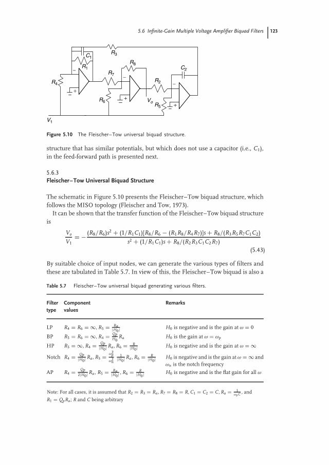
5.6 Infinite-Gain Multiple Voltage Amplifier Biquad Filters 123
+
__
+
_
+
V1
VoR6
R4
R1
C1
R2
R5
R8
R3
R7
C2
Figure 5.10 The Fleischer–Tow universal biquad structure.
structure that has similar potentials, but which does not use a capacitor (i.e., C1),in the feed-forward path is presented next.
5.6.3Fleischer–Tow Universal Biquad Structure
The schematic in Figure 5.10 presents the Fleischer–Tow biquad structure, whichfollows the MISO topology (Fleischer and Tow, 1973).
It can be shown that the transfer function of the Fleischer–Tow biquad structureis
Vo
V1= − (R8/R6)s2 + (1/R1C1)[R8/R6 − (R1R8/R4R7)]s + R8/(R3R5R7C1C2)
s2 + (1/R1C1)s + R8/(R2R3C1C2R7)(5.43)
By suitable choice of input nodes, we can generate the various types of filters andthese are tabulated in Table 5.7. In view of this, the Fleischer–Tow biquad is also a
Table 5.7 Fleischer–Tow universal biquad generating various filters.
Filter Component Remarkstype values
LP R4 = R6 = ∞, R5 = Ra|H0| H0 is negative and is the gain at ω = 0
BP R5 = R6 = ∞, R4 = QpH0
Ra H0 is the gain at ω = ωp
HP R5 = ∞, R4 = Qp|H0| Ra, R6 = R
|H0| H0 is negative and is the gain at ω = ∞Notch R4 = Qp
|H0| Ra, R5 = ω2p
ω2n
1|H0| Ra, R6 = R
|H0| H0 is negative and is the gain at ω = ∞ andωn is the notch frequency
AP R4 = Qp2|H0| Ra, R5 = Ra
|H0| , R6 = R|H0 | H0 is negative and is the flat gain for all ω
Note: For all cases, it is assumed that R2 = R3 = Ra, R7 = R8 = R, C1 = C2 = C, Ra = 1ωpC , and
R1 = QpRa; R and C being arbitrary

124 5 Second-Order Active-RC Filters
universal biquad structure, and the pole frequency and pole Q are given by
ωp =√
R8/R2R3C1C2R7 and ωp/Qp = 1/R1C1 (5.44)
5.7Sensitivity
Sensitivity is a measure of the variability of the performance of a filter as a resultof changes in the values of the components and in the characteristics of the activedevice(s) used to implement the filter. Such changes may occur due to aging,manufacturing tolerances, environmental (i.e., temperature and power supply)variations, and so on. In the previous sections, we have discussed several differentarchitectures for the realization of a second-order active-RC filter. There are manymore structures that have been proposed in this area and an interested reader mayconsult the additional references (Ghausi and Laker, 1981; Schaumann, Ghausi,and Laker, 1990; Schaumann and Van Valkenburg, 2001; Chen, 1986) provided atthe end of this book. Sensitivity is one of the aspects that can be used to comparethe various filter structures with regard to their robustness toward changes in thecomponent values and the characteristics of the active devices used to implementthe filters. Various researchers have aimed their efforts toward minimizing suchsensitivity and thereby have come up with novel filter structures. In the following,we shall introduce the basic definition of sensitivity and illustrate the use of thisdefinition by considering some known filter structures.
5.7.1Basic Definition and Related Expressions
The sensitivity of a function Y with respect to a parameter (or a variable) x isdenoted by SY
x and is defined as
SYx = % change in Y
% change in x= Y
x= dY/Y
dx/x= d(ln Y)
d(ln x)(5.45)
If Y is a function of several variables, Y = f (x1, x2, . . . , xn), then the sensitivity of Yw.r.t. xi is given by
SYxi
= ∂Y/Y
∂xi/xi= ∂(ln Y)
∂(ln xi)(5.46)
In the above, the symbol ∂ implies the partial derivative. Specifically, a sensitivityof 1/2 means that a 5% change in x would bring a 2.5% change in Y. A sensitivityof −1/2 means that a change of +5% in x would cause a change of −2.5% in Y.Several identities that are useful in calculating the sensitivity for complex functionalrelations are listed in Table 5.8.
In general, the filter parameters, such as ωp, will depend upon several componentsthat are used to implement the filter. In such cases, the concept of total differentialis applicable. Thus, if the characteristic F of the filter depends upon several

5.7 Sensitivity 125
Table 5.8 Some basic sensitivity formulas.
Sensitivity Equivalent expression
SkYx , k is a constant SY
x
SY1Y2x S
Y1x + S
Y2x
SY1/Y2x S
Y1x − S
Y2x
SY1/x −SY
x
S1/Yx −SY
x
SaYnx nSY
x
SYx SY
z Szx
parameters (i.e., constituent components) x1, x2, . . . , xn of the filter, we can write
F = ψ(x1, x2, . . . , xn); then, dF =n∑
i=1
∂F∂xi
dxi. Accordingly, the relative change in F
for all the constituent component variations will be
dF
F=
n∑i=1
∂F
∂xi
dxi
F=
∑SF
xi
dxi
xi(5.47)
Thus, the sensitivities with respect to the individual components xi need to becalculated.
Example 5.6. Consider the SK LP filter of Section 5.4.1 with the followingexpressions concerning the pole frequency and pole Q:
ωp = 1/√
R1R3C2C4, ωp/Q p = 1/R3C4 + 1/R1C2 + 1/R3C2 − K/R3C4
To calculate SωpR1
, we can proceed with
ln(ωp) = −(1/2) ln R1 − (1/2) ln R3 − (1/2) ln C2 − (1/2) ln C4.
Taking the partial derivative with respect to R1, we get ∂ωp/ωp = −(1/2)(∂R1/R1).Thus,
SωpR1
= ∂ωp/ωp
∂R1/R1= −(1/2) (5.48a)
It can be similarly shown that
SωpR3
= SωpC2
= SωpC4
= −(1/2) (5.48b)
To evaluate the sensitivity of Qp, one can start with Q p = ωp/P, where P = 1/R3C4 +1/R1C2 + 1/R3C2 − K/R3C4. Then, the sensitivity of Qp, say, with respect to R1,
can be expressed as SQ pR1
= SωpR1
− SPR1
. From the previous results, SωpR1
= −(1/2).Now, ∂P/∂R1 = −(1/R1C2)(1/R1). Hence,
SPR1
= ∂P/P
∂R1/R1= −(1/P)(1/R1C2)
= −(Q p/ωp)(1/R1C2) = −(Q p/R1C2)√
R1R3C2C4 = −Q p
√R3C4/R1C2.

126 5 Second-Order Active-RC Filters
Thus,
SQ pR1
= −(1/2) + Q p
√R3C4/R1C2. (5.49)
The sensitivities of Qp with respect to other parameters can be similarly calculated.It is noted that the sensitivity of Qp is proportional to Qp. So, for a high-Q filter,the SK structure will have a large sensitivity for the pole Q. This informationis important in deciding if one should adopt this architecture or not when thespecifications demand for a design with a high Qp value.
One can consider the clue that the above expressions provide toward a designwith low sensitivity to component variations. Thus, in an ideal situation, we
would like to make SQ pR1
equal to zero. Considering the expression of SQ pR1
above,we see that one has to adjust the components R1, C2, R3, C4 to achieve 0 =−(1/2) + Q p
√R3C4/R1C2, that is, 1/2 = Q p
√R3C4/R1C2. Since Qp and ωp are
dependent on the R,C components, achieving the above condition may be quitechallenging, if not impossible. However, the above discussion simply provides aclue for an approach toward a low-sensitivity design for a specific case.
5.7.2Comparative Results for ωp and Qp Sensitivities
In Table 5.9, we present three different biquad filter structures with expressionsfor the ωp and Qp sensitivities. The structure in (a) is the SK LP SAB filter ofSection 5.4.1, (b) is the IGFMB LP filter of Section 5.5, and (c) corresponds tothe KHN state-variable filter. A discussion regarding the relative merits of thestructures for low-sensitivity design follows.
The entries in Table 5.9 can be used to draw a comparison among the filterstructures in (a)–(c) in that table. We have already noted that the network in theSK filter of (a) has a high sensitivity for Qp. For the IGMFB filter shown in (b), theexpressions for Qp sensitivities with respect to the resistances R1, R2, R3, and Qp aremultiplied by factors that are less than 1/Qp; hence, the products are less than 1.Thus, the Qp sensitivities of the IGMFB filter is less than those in the SK filter.So, the IGMFB filter of (b) in Table 5.9 should be preferred to that of (a) for a lowQp-sensitivity design. For the KHN state-variable filter of (c), all the sensitivities areless than unity. This reveals the superiority of the state-variable filter structure, whena low-sensitivity design is required. In particular, the Qp sensitivities with respect toR5 and R6 could be made zero if R5 and R6 are made equal. In general, state-variablefilters have low sensitivity. However, they require more number of active devicesand network elements (especially resistances), which may add to the cost.
5.7.3A Low-Sensitivity Multi-OA Biquad with Small Spread in Element Values
In Figure 5.11, we present a multi-OA general biquad filter network proposed byMikhael and Bhattacharyya (1975). The sensitivities of ωp, ωz, Qp, and Qz to the

5.7 Sensitivity 127
Tabl
e5.
9Th
ree
diffe
rent
LPst
ruct
ures
and
thei
rω
pan
dQ
pse
nsiti
vitie
s.
Stru
ctur
eEx
pres
sion
sfo
rω
p
and
Qp
ωp
and
Qp
sens
itivi
ties
K
C2
C4
R3
R1
Sal
len
and
Key
LP
str
uctu
re
V1+ −
V2+ −
(a)
ωp
=1
√ R1
R3
C2
C4
1 Qp
=√ R
3C
4R
1C
2+
√ R1
C4
R3
C2
+(1
−K
)√ R1
C2
R3
C4
−SQ
pR
3=
SQ
pR
1=
−(1/
2)+
Qp
√ R3
C4
R1
C2
SQ
pC
2=
−SQ
pC
4=
−(1/
2)+
Qp
( √R
1C
4R
3C
2+
√ R3
C4
R1
C2
)S
ωp
R1
,R3
,C2
,C4
=−(
1/2)
R1
R2
C5
C4
R3
(b)
V2+ −
V1+ −
IGM
FB
LP
str
uctu
reA =
∞− +
ωp
=1
√ R2
R3
C4
C5
1 Qp
=√ C
5C
4
( √R
2R
3R
1+
√ R3
R2
+√ R
2R
3
)S
Qp
R1
=Q
p
( 1 R1
√ R2
R3
C5
C4
)S
Qp
R2
=−
Qp 2
( 1 R1
√ R2
R3
C5
C4
−√ R
3C
5R
2C
4+
√ R2
C5
R3
C4
)S
Qp
R3
=−
Qp 2
( 1 R1
√ R2
R3
C5
C4
+√ R
3C
5R
2C
4−
√ R2
C5
R3
C4
)S
Qp
C4
=−S
Qp
C5
=(1
/2)
Sω
pR
1=
0,S
R2
,R3
,C4
,C5
=−(
1/2)
_ +
_ +
_ +V
1
Vo1
Vo2
Vo3
R3
R6
R1
R2
R5
C1
C2
R4
(c)
KH
N s
tate
-var
iabl
e fil
ter
ωp
=√
R6/R
5R
1R
2C
1C
21 Qp
=1+
R6/R
51+
R4/R
3
√ R5
R2
C2
R6
R1
C1
SQ
pR
1,C
1=
−SQ
pR
2,C
2=
(1/2)
SQ
pR
3=
−SQ
pR
4=
−1/1
+(R
3/R
4)
SQ
pR
5=
−SQ
pR
6=
−Q
p 2R
5−R
61+
R4/R
3
√R
2C
2R
5R
6R
1C
1
Sω
pR
1,R
2,R
5,C
1,C
2=
−Sω
pR
6=
−(1/
2),S
ωp
R3
,R4
=0

128 5 Second-Order Active-RC Filters
C1
C2
R10
R2
R7
R8−
−
++
−
+
R4R3
R6R5
R9
Vs
R1
V1
V2
V3
Figure 5.11 Mikhael–Bhattacharyya multiple amplifier biquad structure.
passive components are all less than unity. The network uses both the invertingand noninverting inputs of the OA. The transmission zeroes are realized withfeed-forward resistive network. For a given pole Q, the spread in the resistancevalues (using equal capacitance values) is proportional to only Q1/2, while mostother biquad structures require resistance spreads of the order of Q or Q2.
The transfer functions for the two most useful output terminals, assuming idealOA, are
V1
Vs=
s2
[G1
(1 + G4
G9
)− G2G3
G9
]+ s
G3G7G8
G9C1
+ G7G10
C1C2
[(1 + G4
G9
)G5 − G3G6
G9
]/D(s) (5.50)
V3
Vs=
s2G1 + s
G7G8
G9C1
[(1 + G2
G7
)G3 − G1G4
G7
]
+ G7G10
C1C2
[(1 + G2
G7
)G5 − G4G6
G7
]/D(s) (5.51)
where Gi = 1/Ri, and
D(s) = s2(G1 + G2) + sG7G8
G9C1(G3 + G4) + G7G10
C1C2(G5 + G6) (5.52)
Thus,
ωp =√
G7G10
C1C2
G5 + G6
G1 + G2and Q p = R3R4R8
R9(R3 + R4)
√R7C1(R1 + R2)(R5 + R6)
R6R10C2R1R2R5
(5.53)
For details regarding this circuit, we refer the reader to Mikhael and Bhattacharyya(1975).

5.7 Sensitivity 129
5.7.4Sensitivity Analysis Using Network Simulation Tools
In Section 5.7.1, we have dealt with finding analytical expressions for the sensitivityfunctions for a given filter network. When numerical values are required, one canplug in appropriate element values in the pertinent expression to arrive at thenumerical value. If, however, the analytical expressions are not readily available,network simulations tools such as SPICE, PSpice, or HSPICE can be used toarrive at the numerical value of the sensitivity. In such a case, the component withrespect to which the sensitivity is required can be assigned a variable parametervalue and the filter performance function (such as ωp and Qp) can be evaluated asa function of this variable parameter. The sensitivity value can then be calculatedby using the results (i.e., postprocessing) of pertinent simulations. Figure 5.12shows the schematic of a fourth-order Chebychev BP filter realized using a cascadeof two biquadratic filters. Each biquad is realized using the multiple feedbackinfinite-gain amplifier configuration, as discussed in Section 5.5 of this chapter.We are interested in evaluating the sensitivity of the center frequency ωo of the filterwith respect to the resistance R16 whose nominal value is 6.34 k. The variationin the value of R16 is assumed to be 10%. Thus, its value could lie between 5.71and 6.97 k. In a typical network simulation using PSpice, one can assign R16
as a variable parameter with values such as 5.71, 6.34, and 6.97 k. The centerfrequency of the BP response can be evaluated as a function of this parameter andthereafter the ratio ωo/ωo
R16/R16(nominal) can be calculated. This ratio is the sensitivityof the center frequency ωo with respect to R16. A plot of the variation of ωo as
+−
+−
+−
V−
V1
V2 V3
V−
V+
V+V+
V−
+
−
R1793.1
18.2kR18
10nC13
42
8
1
rvalR16
rvalParameters:
C9 C10
6.34k
10n
LT1013/LT
V−
V−
V+
V
V+
+
−
R21110
22.1kR20
10nC11
42
8
11
3
6.34kR19
10n
LT1013/LT
U3A
Out
3U1A
0
0
Figure 5.12 Schematic of a fourth-order filter using a cascade of two biquad filters.

130 5 Second-Order Active-RC Filters
10.040K5.6K 5.8K 6.0K 6.2K
rval
6.4K 6.6K 6.8K 7.0K
10.044K
10.048K
10.052K
CenterFreq (U(OUT), 0.5)
Figure 5.13 Variation of the center frequency ωo of the BPfilter of Figure 5.12 as a function of the resistor R16.
a function of the variable parameter R16 obtained from the Pspice simulation ispresented in Figure 5.13.
5.8Effect of Frequency-Dependent Gain of the OA on the Filter Performance
Until now, we have assumed the OA used to realize the filters as ideal. It iswell known that a practical OA is far from ideal. The open-loop gain is finiteand changes with frequency. Since the filter is a frequency-selective device, thefrequency-dependent gain of the OA can have a considerable impact on theperformance of an active-RC filter. In this section, we present an analyticaltechnique to take care of the frequency-dependent gain of an OA used as a buildingblock for a filter. The technique will be illustrated by considering the case of abiquadratic filter.
5.8.1Cases of Inverting, Noninverting, and Integrating Amplifiers Using an OA withFrequency-Dependent Gain
5.8.1.1 Inverting AmplifierConsider the amplifier shown in Figure 5.14. Application of KCL leads to
(Vi − Vx)G1 = (Vx − Vo)G2

5.8 Effect of Frequency-Dependent Gain of the OA on the Filter Performance 131
R2
AVi Vx
Vo
R1
+
−
Figure 5.14 An inverting voltage amplifier whose gain is afunction of the OA finite gain A.
But, Vx = −Vo/A. Substituting this in the above equation, we get ViG1 =−Vo
[G2 + G1+G2
A
].
The amplifier voltage gain then becomes
K− = Vo
Vi= − G1
G2 + 1A (G1 + G2)
= Ko1
1 + 1A
(1 + R2
R1
)or
K− = Ko1
1 + K1A
(5.54a)
where Ko = −R2/R1 is the inverting amplifier gain when the OA has the idealopen-loop gain of infinity; K1 is the gain of the noninverting amplifier realized withan ideal OA.
5.8.1.2 Noninverting AmplifierFigure 5.15 presents the noninverting amplifier using an OA of gain A. The KCLequations VxG1 + (Vx − Vo)G2 = 0 and Vx(G1 + G2) = VoG2x(G1 + G2) = VoG2
together with Vo = A(Vi − Vx) will lead to
K+ = Vo
Vi= G1 + G2
G2
1
1 + 1A
G1+G2G2
Finally, since Gi = 1/Ri, we have
K+ = K11
1 + K1A
(5.54b)
A
Vi
Vx
Vo
R1
R2
+
−
Figure 5.15 A noninverting voltage amplifier whose gain isa function of the OA finite gain A.

132 5 Second-Order Active-RC Filters
where K1 is the gain of the noninverting amplifier with ideal OA.
5.8.1.3 Inverting Integrating AmplifierFollowing methods similar to the above, one can derive the gain of an invertingintegrating amplifier realized with an OA of gain A, as
T(s) = Vo(s)
Vi(s)= TI(s)
1
1 + 1A (1 − TI(s))
(5.55)
where TI(s) = − 1sCR , the integrator gain function with an ideal OA.
From the above derivations, it is clear that when the OA has a frequency-dependent gain A = A(s), all the gain functions K−, K+, and T(s) become frequencydependent to a certain degree. One can therefore use, in general,
K− = K0M1(ω) exp(−jφ1)
K+ = K1M2(ω) exp(−jφ2) (5.56)
T( jω) = TI( jω)M3(ω) exp(−jφ3)
In the above, the explicit natures of the M and φ functions will depend upon thespecific model used to represent the frequency-dependent gain A(s) of the OA.Thus, with an integrator model for A(s), that is, A(s) = ωt/s, s = jω, one can derive
M1(ω) = 1√1 + (K1ω/ωt)2
= M2(ω), φ1(ω) = tan−1
(K1ω
ωt
)= φ2(ω), and
M3(ω) = 1√1 + (ω/ωt)2
, φ3(ω) = tan−1
(ω
ωt
)(5.57)
In the above, ωt is the gain-bandwidth (GB) value of the OA. In deriving M3 andφ3, the assumption 1/(ωtCR) 1 has been used.
The technique to analyze an active filter realized with an OA that has afrequency-dependent gain function involves (i) identification of the basic modeof operation of the OA in the filter (i.e., inverting or noninverting amplifier or inte-grating amplifier) and then (ii) employing the pertinent gain function as discussedin Sections 5.8.1.1–5.8.1.3 and summarized in the form presented in Eq. (5.56).The technique is illustrated by considering a specific case.
5.8.2Case of Tow–Thomas Biquad Realized with OA Having Frequency-Dependent Gain
Consider Figure 5.16, which shows the Tow–Thomas filter in its basic form.By inspection, we can understand that OA 1 and 2 are functioning as invertingintegrators and OA 3 is working as an inverting amplifier.
Considering the OA to be ideal, one can write the following equation for thesignal V2:
V2 = − Vs
sC1R4− V2
sC1R1− V1
sC1R3(5.58a)

5.8 Effect of Frequency-Dependent Gain of the OA on the Filter Performance 133
_
++
_
+
Vs
OA 1 OA 2 OA 3
Vx
R4
R1
V2 V1
R2r1
r2
C2
R3C1
Figure 5.16 The Tow–Thomas filter in its basic form.
But
V1 = − r2
r1Vx and Vx = − 1
sC2R2V2 (5.58b)
Now, considering the frequency-dependent gain function of the OA, we rewrite theabove equation as
V2 = − Vs
jωC1R4M3 exp(−jφ3) − V2
jωC1R1M3 exp(−jφ3)
− V1
jωC1R3M3 exp(−jφ3) (5.59a)
But
V1 = − r2
r1M1 exp(−jφ1)Vx and Vx = − 1
jωC2R2V2M3 exp(−jφ3) (5.59b)
In the above, we have assumed that all the OAs are identical. M1, M3, φ1, and φ3
have the same significance as explained in Eq. (5.56). Writing Ko = (r2/r1) andcollecting all terms involving V2 on one side, we have
V2
[1 + M3 exp(−jφ3)
jωC1R1+ Ko
−ω2C1R3C2R2M2
3M1 exp(−j(2φ3 + φ1))]
= − Vs
jωC1R4M3 exp(−jφ3) (5.60)
On further simplification, we get the transfer function, V2(jω)/Vs(jω) = N(jω)/D(jω),where
N( jω) = − jω
C1R4M3 exp(−jφ3) (5.61a)
D( jω) = −ω2 + jω
C1R1M3 exp(−jφ3) + Ko
C1C2R2R3M2
3M1 exp(−j(2φ3 + φ1))
(5.61b)
In order to find the pole frequency and pole Q under this new condition, one hasto expand D(jω) by writing exp(jx) = cos(x) + jsin(x). Then,
D( jω) = −ω2 + ωM3
C1R1sin(φ3) + KoM2
3M1
C1C2R2R3cos(2φ3 + φ1) + j
[ωM3
C1R1cos(φ3)
− Ko
C1C2R2R3M2
3M1 sin(2φ3 + φ1)]
(5.62)

134 5 Second-Order Active-RC Filters
When ω equals the pole frequency ωp, one must have Re(D( jω)) = 0. The new polefrequency is obtained by solving the quadratic equation in ω
0 = −ω2 + ωM3
C1R1sin(φ3) + KoM2
3M1
C1C2R2R3cos(2φ3 + φ1) (5.63)
If the GB of the OA is very large (20 times or more) compared to the ideal pole
frequency ωp =√
KoC1C2R2R3
, one can expect the phase angles φ1 and φ3 to be small.
Then, approximately
ωp∼= ωpM3
√M1 cos(2φ3 + φ1) (5.64)
The new pole frequency will thus be smaller than the nominal (i.e., with ideal OA)pole frequency ωp. To find the new Qp →Qp, we recall that the coefficient of s = jωterm in D(s) of the standard biquadratic transfer function is ωp/Qp. Then, in Eq.(5.62), we have to pay attention to the imaginary part of D(s), since this could beput in the form
jω
[M3
C1R1cos(φ3) − Ko
ωC1C2R2R3M2
3M1 sin(2φ3 + φ1)]
and be related to jω
(ωp
Qp
). Again, in case of an ideal OA, ωp/Qp = 1/C1R1. Thus,
ωp
Qp
= ωp
Q pM3 cos(φ3) − ω2
pM23M1 sin(2φ3 + φ1)
ω(5.65)
The above leads to (assuming ω ∼= ωp)
Qp∼= ωp
(ωp/Q p)M3 cos(φ3) − ωpM23M1 sin(2φ3 + φ1)
(5.66)
Finally, using the ratio of ωp/ωp from Eq. (5.69), we get
Qp = Q pM3
√M1 cos(2φ3 + φ1)
M3 cos(φ3) − Q pM23M1 sin(2φ3 + φ1)
(5.67)
Equation (5.67) indicates that the new pole Q (i.e., Qp) could become higher than theideal (i.e., with ideal OA) Qp if the denominator becomes less than the numerator.This is known as Q-enhancement caused due to the frequency-dependent gainfunction of the OA. Further, Qp can even become negative if the denominatorin Eq. (5.67) becomes negative. A negative pole Q implies a positive real part forthe poles of the second-order filter. A positive real part will produce an unstablesystem. Thus, when the OA has a frequency-dependent gain, the pole Q willin general show an increase from the nominal value and the system may evenbecome unstable when the filter requires a high Qp design and if the GB of theOA is not substantially higher than the nominal pole frequency ωp.
A rule of thumb for avoiding the above degradations due to a finite,frequency-dependent gain of the OA is to choose an OA whose GB is at least 20times higher than the design ωp. Further, before embarking on the design task,one must estimate the enhancement in the value of Qp by employing Eq. (5.67).A known model for the OA gain function A(s) has to be used for this purpose.
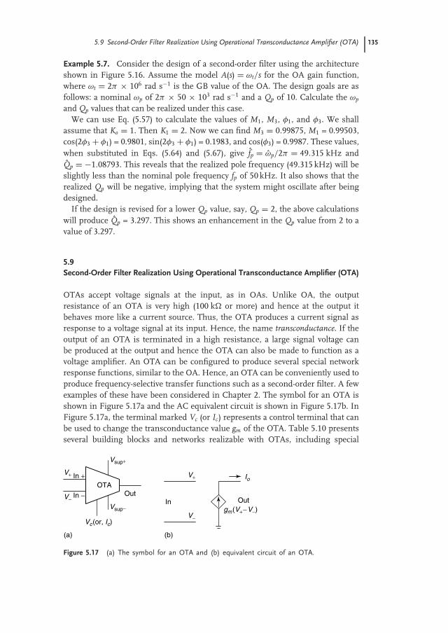
5.9 Second-Order Filter Realization Using Operational Transconductance Amplifier (OTA) 135
Example 5.7. Consider the design of a second-order filter using the architectureshown in Figure 5.16. Assume the model A(s) = ωt/s for the OA gain function,where ωt = 2π × 106 rad s−1 is the GB value of the OA. The design goals are asfollows: a nominal ωp of 2π × 50 × 103 rad s−1 and a Qp of 10. Calculate the ωp
and Qp values that can be realized under this case.We can use Eq. (5.57) to calculate the values of M1, M3, φ1, and φ3. We shall
assume that Ko = 1. Then K1 = 2. Now we can find M3 = 0.99875, M1 = 0.99503,cos(2φ3 + φ1) = 0.9801, sin(2φ3 + φ1) = 0.1983, and cos(φ3) = 0.9987. These values,when substituted in Eqs. (5.64) and (5.67), give fp = ωp/2π = 49.315 kHz andQp = −1.08793. This reveals that the realized pole frequency (49.315 kHz) will beslightly less than the nominal pole frequency fp of 50 kHz. It also shows that therealized Qp will be negative, implying that the system might oscillate after beingdesigned.
If the design is revised for a lower Qp value, say, Qp = 2, the above calculationswill produce Qp = 3.297. This shows an enhancement in the Qp value from 2 to avalue of 3.297.
5.9Second-Order Filter Realization Using Operational Transconductance Amplifier (OTA)
OTAs accept voltage signals at the input, as in OAs. Unlike OA, the outputresistance of an OTA is very high (100 k or more) and hence at the output itbehaves more like a current source. Thus, the OTA produces a current signal asresponse to a voltage signal at its input. Hence, the name transconductance. If theoutput of an OTA is terminated in a high resistance, a large signal voltage canbe produced at the output and hence the OTA can also be made to function as avoltage amplifier. An OTA can be configured to produce several special networkresponse functions, similar to the OA. Hence, an OTA can be conveniently used toproduce frequency-selective transfer functions such as a second-order filter. A fewexamples of these have been considered in Chapter 2. The symbol for an OTA isshown in Figure 5.17a and the AC equivalent circuit is shown in Figure 5.17b. InFigure 5.17a, the terminal marked Vc (or Ic) represents a control terminal that canbe used to change the transconductance value gm of the OTA. Table 5.10 presentsseveral building blocks and networks realizable with OTAs, including special
OutOut
In +
InIn −
OTA
Vc(or, Ic)
gm(V+−V−)
Io
Vsup−
Vsup+
V+ V+
V−
V−
(a) (b)
Figure 5.17 (a) The symbol for an OTA and (b) equivalent circuit of an OTA.

136 5 Second-Order Active-RC Filters
Table 5.10 Building blocks and network elements realizableusing OTAs (Geiger and Sanchez-Sinencio, 1985; Su, 1996).
Network Function Comment
A
Zin
_
gm+
Zin = 1gm
Grounded resistance of 1gm
. If the input and groundterminals are reversed, weget a negative resistance of
1gm
B
Zin
gm1
gm2
+
+
gm1 = gm2 =gm
Zin = 1gm
Floating resistance of 1gm
.
If the input and ground ter-minals are reversed, we geta negative floating resistanceof 1
gm
C
Vi Vo
CL
gm−
+VoVi
= gmsCL
Voltage integrator
D
Ci
Ii
Io
gm−
+
↓
→ IoIi
= gmsCi
Current integrator
E
C
Vi
VOgm2
+
−gm1
−
+ VoVi
= gm1sC+gm2
Lossy voltage integrator

5.9 Second-Order Filter Realization Using Operational Transconductance Amplifier (OTA) 137
Table 5.10 (continued).
Network Function Comment
FVi
VOgm2
+
−gm1
−
+VoVi
= gm1gm2
Voltage amplifier
G
V2
V1
.
.
.Vn
VO
gmn−
+
gm2−
+
gm1−
+
gm2
+
−Vo =
1gm
n∑i=1
gmiVi
Weighted summer
HVi
C1
C2
Vogm1
−
+
gm2+
−
VoVi
=sC1+gm1
s(C1+C2)+gm2
First-order section
I
Zin ZL
gm1−
+
gm2−
+
Zin =1
gm1gm21
ZL
Grounded positive imped-ance inverter. If ZL is a ca-pacitor of C Farads, then Zin
reflects a grounded inductorof value C/(gm1gm2) H.
J
ZinZL
gm1−
+
gm3−
+
gm2−
+
gm2 =gm3Zin =
1gm1gm2
1ZL
Floating positive impedanceinverter. If ZL is a capacitorof C Farads, then Zin reflectsa grounded inductor of valueC/(gm1gm2) H.

138 5 Second-Order Active-RC Filters
network elements such as a gyrator, FDNR, and so on. These building blocksand functional elements can be conveniently utilized to produce fully monolithiccontinuous-time filters using an available IC technology. In the ac equivalentcircuit, the OTA has been assumed as ideal, that is, with an infinite input resistanceand an output resistance. Also, it is assumed that no parasitic capacitances arepresent.
5.9.1Realization of a Filter Using OTAs
On examining the networks in Table 5.10, one may appreciate that an OTA can beconverted to a resistance by simply connecting the output to the input (entries A,B in Table 5.10). This is the same principle as that used to implement an activeresistance from a BJT or MOS transistor. Thus, the RC-active filters realized withOAs can now be realized using capacitors, OTAs connected as resistors, and OTAconnected as a voltage amplifier. This gives rise to what is popularly known asOTA-C filters or gm − C filters. It may also be noted that since an OTA and a capacitorare easily available in an IC technology, OTA-C filters easily render themselvesto monolithic realizations. It should be noted that OTA-C filters can be designedto work at frequencies of the order of tens of hundreds of megahertz; they arephysically small and consume low power.
5.9.2An OTA-C Band-Pass Filter
Consider Figure 5.18a, whose equivalent circuit is shown in Figure 5.18b.KCL at node b gives
(Vi − Vb)sC1 − gm1Vo = 0 (5.68)
and KCL at node a gives
gm2Vb − gm3Vo = VosC2 (5.69)
Eliminating Vb from the above two equations, we have the VTF Vo(s)/Vi(s) to be
Vo(s)Vi(s)
= sgm2C1
s2C1C2 + sgm3C1 + gm1gm2(5.70)
This represents a BP filter. On comparing with the standard biquadratic transferfunction (Table 5.2), we can identify
ωp =√
gm1gm2
C1C2,
ωp
Q p= gm3
C2, therefore Q p =
√C2
C1
√gm1gm2
gm3(5.71)
It should be noted that in an OTA-C filter the design parameters are the capacitanceC (an electrical element) and gm (a network function). The gm has to be realized byusing appropriate electrical control voltage or current signals.

5.9 Second-Order Filter Realization Using Operational Transconductance Amplifier (OTA) 139
C1
C2
C2
ViVo
a
b
(a)
(b)
+
_
C1Vi
b a
a Va
Vb
Vo = Va
gm1+
−
gm2
−gm1Va
gm2Vb −gm3Va
−
+
gm3+
−
Figure 5.18 An OTA-C BP filter; (a) schematic, (b) AC equivalent circuit.
5.9.3A General Biquadratic Filter Structure
Figure 5.19a presents a structure, which can be used to realize any of the fivestandard biquadratic transfer functions. It consists of five OTAs. The analysis canbe carried out by considering the AC equivalent circuit shown in Figure 5.19b. Byinspection, we have
iC1 = gm5VA − gm1Vo (5.72a)
Vx = iC1
sC1= gm5VA − gm1Vo
sC1(5.72b)
KCL at node Vy leads to
gm2Vx + gm4VB − gm3Vo = sC2(Vo − VC) (5.73)
Substituting for Vx from Eq. (5.77b), and simplifying, we get
Vo = s2VC + (gm4/C2)sVB + (gm2gm5/C1C2)VA
s2 + (gm3/C2)s + (gm1gm2/C1C2)(5.74)
Comparing the denominator of Eq. (5.79) with the standard biquadratic form, weget
ωp =√
gm1gm2
C1C2,ωp
Q p= gm3
C2(5.75a)

140 5 Second-Order Active-RC Filters
(a)
(b)
C1
C2
VAVB
VC
Vo
_
gm1+
+
+gm4
−+gm5
−
_
gm3+
gm2−
gm2Vxgm5VA
_gm1Vy C1
iC1
Vx
+
_
VB
+
_
VA
↓
Vy = Vo
_gm3Vy
gm4VB
C2
VC
+
−
Figure 5.19 (a) A universal biquad filter using five OTAs and (b) equivalent circuit of (a).
and
Q p = 1gm3
√gm1gm2C2
C1(5.75b)
On examining Eq. (5.74), it is obvious that, by appropriately choosing the signalvoltages VA, VB, or VC, we can realize different transfer functions. Thus
For an LP filter: choose VB = VC = 0 (5.76)
For an HP filter: choose VA = VB = 0 (5.77)
For a BP filter: choose VA = VC = 0 (5.78)
For a notch filter: choose VB = 0, VA = VC (5.79)
For an AP filter: choose VA = VB = VC = Vi, gm1 = gm5, and gm2 = gm4.
(5.80)
5.10Technological Implementation Considerations
In the early stages of active-RC filters, the filters were made using OAs and discreteRC elements mounted together on a printed circuit board (PCB). As the impetus

5.10 Technological Implementation Considerations 141
toward miniaturization gained momentum, hybrid technology was adopted for theimplementation of active-RC filters.
In hybrid technology, the OA dies and the discrete components are bonded ina single package. Special materials and techniques are used to implement theresistances and capacitances. In thick film technique, resistances are preparedfrom a paste of conducting particles and glass, deposited on an insulating surface.The physical sizes can be a lot smaller than that of the discrete resistances. Thesheet resistance of a thick film paste ranges between 1 /square and 10 M/square(Chen, 1995). Thus, a large range (0.5 to 1 G) of resistances can be realized.The tolerance (20–30%) and the temperature coefficient (50–100 ppm/K) of theresistances are, however, rather large. The tolerance could be greatly reduced inthin film technology, where the resistances are made from thin films of metalalloys deposited on an insulating surface (i.e., glass). Thin film circuits are muchsmaller than thick film circuits. The available resistance range is, however, smaller.The sheet resistance value is of the order of 10–200 /square, leading to a nominalresistance value ranging from 10 to 10 M. The temperature coefficient ofresistance (TCR) is of the order of 15–150 ppm/K and the absolute tolerance istypically between 5 and 10%. To obtain high nominal resistance, the resistive layeris specially shaped by laser trimming. This process, however, increases the cost ofproduction of the resistance. Capacitances are also available in hybrid technology,but mostly resistances using either thick- or thin film techniques have been usedin hybrid technological production of an active-RC filter.
Advancements in semiconductor process IC technology leading to on-chip OTAdevices opened up the possibilities of implementing an active filter entirely ona monolithic substrate. In this respect, it is useful to know about the R and Celements as are available in a given IC technology. Brief discussions on thesefollow.
5.10.1Resistances in IC Technology
In its simplest form, a resistance is formed by a rectangular layer of semiconduc-tor material, with a specified sheet resistance (resistance per square). The totalresistance is equal to the number of squares multiplied by the sheet resistance.For a resistance of large value, an economy in substrate area can be achievedby adopting a serpentine (meandered) structure. An accurate estimation of theresistance requires use of conformal mapping technique.
5.10.1.1 Diffused ResistorUsually, the diffusion layers in a transistor process can be used to implementresistors. Thus, in a BJT process, the base, emitter, or collector diffusion can beemployed to build resistors. The most preferred one is the base-diffused resistor.A typical geometry and the electrical model are shown in Figure 5.20 (Grebene,1984). For good matching tolerance, a large width should be used for the diffusionlayer. Base-diffused resistors with 50-µm resistor width can achieve a matching

142 5 Second-Order Active-RC Filters
pp p
p substraten+ buried
Epitaxial nBase
Resistor contacts Epitaxial (tub) contact
Most positive
Epitaxial (tub) contact
(b)
(a)
Bulk
Voltage
Figure 5.20 (a) Cross section and (b) electrical circuit model of a typical diffused resistor.
tolerance of ±0.2%. The sheet resistance ranges between 100 and 200 /square.The TCR ranges between 1500 and 2000 ppm/
C.
5.10.1.2 Pinched ResistorTo obtain a relatively high value of the sheet resistance (and, hence, to build aresistor of high value with less area), the base diffusion area is pinched, leadingto pinched diffused resistors. The sheet resistance that can be realized falls in therange of 2–10 k/square. The pinching is obtained, for example, by diffusing ann+ diffusion layer over a p-type base diffusion. The emitter diffusion greatly reducesthe effective cross section (i.e., pinches) of the p-type resistor, thereby raising itssheet resistivity. Figure 5.21 shows a geometrical sketch of a p-type base pinchedresistor. The process tolerance is very poor, ranging to a maximum of ±50%.
5.10.1.3 Epitaxial and Ion-Implanted ResistorsLarge values of resistance can also be obtained by using low doping concentrationthat forms the bulk of the resistor. Thus, an epitaxial resistor uses the bulkresistance of the n-type epitaxy in the BJT process. The p-type base diffusion can be
ppp base
p substraten+ buried
Epitaxial n
Resistor contacts
n+ emitterPinched area
Figure 5.21 Cross section of a typical pinched resistor.

5.10 Technological Implementation Considerations 143
n+
n+
Optional p-diffusion
n epitaxial
p substrate
Resistor contacts Resistor contacts
SiO2SiO2
n epitaxial
p substrate
n+
p diffusion
p implantEpi contact
(a) (b)
Figure 5.22 Cross section of (a) epitaxial and (b) ion-implanted resistors.
used to pinch the cross section of the epitaxial resistor, thereby leading to a pinchedepitaxial resistor. For an epi thickness of 10 µm and a doping concentration of 1015
donor atoms per cubic centimeter, an effective sheet resistance of 5 k/squarecan be obtained. The TCR value for epitaxial resistor is rather high, being of theorder of 3000 ppm/
C.An ion-implanted resistor can be built using a very thin layer of implant
(0.1−0.8 µm), which leads to a very high value of sheet resistivity compared to thatof the ordinary diffused resistors. Commonly used impurities are the p-type boronatoms. A sheet resistance of 100–1000 /square can be obtained. The matchingtolerance is very good, being typically within ±2%. The TCR is controllableto ±100 ppm/
C. Figures 5.22a and 5.22b, respectively, show the geometricalstructures of epi and ion-implanted type of resistors.
5.10.1.4 Active ResistorsActive resistance implies resistance obtained from active devices, that is, transistors.Considering the I–V characteristics of well-known active devices, that is, BJT andMOS transistors, one can easily see that the devices exhibit the behavior of aresistance in certain areas of the I–V characteristics. For the BJT, it is the saturationzone, while for the MOS it is the linear zone. This is illustrated in Figure 5.23.
The advantages of an active resistance compared with a passive semiconductorresistance are twofold: (i) the available resistance can be very large without requir-ing large area of the substrate and (ii) the value of the resistance can be changed
IC
IC ID
ID
VCE VDS(a) (b)
Figure 5.23 Current–voltage characteristics of (a) BJTand (b) MOS transistors pertaining to implementation ofresistors.

144 5 Second-Order Active-RC Filters
VC
vD vD vD−
iD−
vS−vS vS
VSS VSS
VC
VSS
iD
(a) (b)
↓iD↓ ↓
Figure 5.24 Active resistor (a) with a single MOS transistorand (b) with MOS transistors in differential configuration.
by a control voltage or current. In the modern MOS and CMOS technology, MOStransistors working in the linear region are frequently used to produce a resistance.Considering the N-type metal-oxide semiconductor (NMOS) transistor inFigure 5.24a, the instantaneous (i.e., AC plus DC) drain–source current, assumingoperation in the linear (ohmic) region, can be modeled by the level = 1 equation:
iD = Kn[2(VC − vS − VThn)(vD − vS) − (vD − vS)2] (5.81)
In the above, Kn is the transconductance parameter, VThn is the thresholdvoltage, and VC is the DC control voltage applied to the gate of the NMOStransistor. The operation of the transistor is in the linear (ohmic) region so thatvD − vS ≤ VC − vS − VThn is true. The drain–source conductance is given by ∂iD
∂vDSand the associated resistance (RMOS) is the inverse of this value. Since in an MOStransistor, Kn is proportional to the width-to-length ratio (W/L) of the transistor, itis clear that RMOS is inversely proportional to W and, hence, by choosing a narrowwidth transistor, a large RMOS can be realized. In the differential configuration ofFigure 5.24b, the nonlinear term in RMOS gets cancelled out and one can derivethe differential resistance value as
R = 1
µnCox (VC − VThn)
(L
W
)= Rsh
(L
W
), where Kn = 1
2µnCox
(W
L
)(5.82)
With µnCox = 25 µA V−2 and VC − VThn = 1 V, a value Rsh = 40 k can berealized.
5.10.2Capacitors in IC Technology
Capacitor structures available in monolithic form include pn junction, MOS,and polysilicon capacitors. Silicon dioxide or silicon nitride sandwiched betweentwo layers of doped (n- or p-type) silicon forms the basis of capacitors in atypical IC technology. These, however, need extra masking steps. More naturallyoccurring capacitors are formed between semiconductor junctions, for example, inBJT process technology. In any case, typical values are very small (viz., 0.05–0.5pF/mil2) (Grebene, 1984) and values larger than 10 pF are not practical because ofthe large substrate area consumed.

5.10 Technological Implementation Considerations 145
5.10.2.1 Junction CapacitorsApplication of a reverse bias across a semiconductor junction results in a depletionlayer that is devoid of mobile carriers. The situation closely resembles two parallelplates separated by a dielectric of width equal to the width of the depletion area. Thearea of the parallel plate is the total junction area. A typical analytical expressionfor the capacitance per unit area takes the form C = Cxo/(1 + V/Vt)
n, where Cxo isthe zero bias capacitance (per unit area), Vt is the built-in junction potential, andthe exponent n is dependent on the profile of the junction transition. This changesbetween 1/2 and 1/3, as the transition contour changes from a step junctionto a linearly graded junction. As in a semiconductor resistor, a capacitor builtusing a semiconductor process is far from ideal. Thus, it will have few parasiticcomponents arising out of the properties of the semiconductor layers. In a BJTprocess, three capacitors are available (see Figure 5.25), and CBC is mostly used forpractical purposes. CCS is essentially a parasitic capacitance and is not convenientlymeasurable. CEB can give relatively high value (0.001 pF/µm2) of capacitance buthas a small breakdown voltage. CBC has a higher break down voltage, but a smallervalue for capacitance (2.3 × 10⁻⁴ pF/µm2) compared with CEB (Grebene, 1984).
5.10.2.2 MOS CapacitorsAn MOS capacitor is formed between the n+ diffusion (deposited while creatingthe channel region) and an aluminum (or polysilicon) layer with a layer of SiO2
deposited (500–1000 A) in between them. Sometimes, the silicon nitride layer isused as dielectric because of slightly higher dielectric constant (4–9) than silicondioxide (2.7–4.2). A typical cross section and the electrical model are shown inFigure 5.26 (Grebene, 1984).
p− substrate
n+
np p pn+ (emitter)(base)
Collectorb
(Bipolar transistor)
BE
C
Substrate
CBC
CCS
CEB
(Electrical model for the junction capacitances)
(a)
(b)
e
Figure 5.25 (a) Cross section of a BJT transistor and (b)electrical circuit model showing the junction capacitors.

146 5 Second-Order Active-RC Filters
n+
p− (substrate)
Thinox(ide)Plate 1 Plate 2
Field oxide (FOX)FOX
C
D Cp
Plate 1 Plate 2
Substrate(a) (b)
R
Figure 5.26 Basic MOS capacitor: (a) cross section and (b) electrical circuit model.
It may be noticed that, while C is the desired capacitance, it is invariably associatedwith parasitic components like R, Cp, and a diode D.
5.10.2.3 Polysilicon Capacitor
Polysilicon capacitors are conveniently available in metal-oxide semiconductor fieldeffect transistor (MOSFET) technology, where the gate of the MOSFET transistor ismade of polysilicon material. Figure 5.27a shows a typical structure of a polysiliconcapacitor, where a thin oxide is deposited on top of a polysilicon layer and serves as aninsulating layer between the top-plate metal layer and the bottom-plate polysiliconlayer. The polysilicon region is isolated from the substrate by a thick oxide layer thatforms a parasitic parallel-plate capacitance between the polysilicon layer and the sub-strate. The equivalent circuit model, which reflects this, is shown in Figure 5.27b.
5.10.3Inductors
Interest in monolithic inductors has been on the increase with the availabilityof submicron CMOS IC technology. Initially, the role of active-RC filters was toreplace the use of inductances. The signal processing case was for low frequencies
Capacitorcontact Polycontact
PolysiliconThinox
SiO2
p substrate
CR
Cox
Substrate(a) (b)
Figure 5.27 MOS polysilicon capacitor: (a) cross section and (b) electrical circuit model.

5.10 Technological Implementation Considerations 147
Via
Metal 1Metal 2
Figure 5.28 Typical layout of a spiral inductor in CMOS IC technology.
(300 Hz to 3.4 kHz) and the inductors usable at these frequencies were too bulky.As the feature size of the transistors in the IC technology shrunk, the possibilitiesof processing high-frequency signals on a monolithic substrate came into play. Atthese frequencies (300 MHz and more), the inductors needed are small in value(nano henries) and can be easily laid out using the metal lines available in amodern IC technological process. Both rectangular and circular spiral patternshave been used for signal processing at frequencies of 900 MHz and more (Nguyenand Meyer, 1990). A typical pattern for a rectangular spiral monolithic inductoris shown in Figure 5.28 (Chen, 1995). Laying two such independent patterns inan interleaved way can produce a transformer on a monolithic substrate. Like amonolithic capacitor, the use of a monolithic inductor is primarily limited by thesubstrate area that it will occupy. Practical limits are expected to be around a valueof 10 nH.
5.10.4Active Building Blocks
5.10.4.1 Operational Amplifier (OA)
OA is the most important and most widely used building block in active filter design(Geiger, Allen, and Strader, 1990; Johns and Martin, 1997; Baker, Li, and Boyce,1998). The desired characteristics of an OA, for the design of a filter, are very highinput impedance, high open-loop gain, very wide gain-bandwidth product value,and very low output impedance. Other important characteristics are low offsetvoltage, high common-mode rejection ratio (CMRR) and power supply rejectionratio (PSRR), high slew rate, low settling time, and large dynamic range. Severalexcellent designs of OA have been reported in the literature. Many high-quality OAsare available as commercial products. Examples are AD648, HA 2600, LM 101, andµA 741 chips. One typical realization is shown in Figure 5.29. This implementationuses a 5-µm CMOS process; the transistor dimensions are shown in Table 5.11(Toumazou, Lidgey, and Haigh, 1990). This OA uses a bias current of 25 mA with±5 V supply. The open-loop gain is about 73 dB and the GB value is 2.2 MHz. Thefirst corner frequency (for one-pole model) is at 400 Hz.

148 5 Second-Order Active-RC Filters
VDD
VSS
Rbias
Vin+Vin−
C
M1 M2
M3 M4
M5
M6
M7
M8
M9
M10
M11
M12
M13
M14
Vout
Ibias
↓
Figure 5.29 A typical realization of an OA (adapted from Toumazou et al., 1990).
Table 5.11 Geometric dimensions of the OA shown in Figure 5.29.
Transistor M1 M2 M3 M4 M5 M6 M7 M8 M9 M10 M11 M12 M13 M14
W (µm) 120 120 50 50 150 95 150 135 207.5 135 402.5 7.5 7.5 150L (µm) 7 7 10 10 10 10 10 5 5 5 5 15 5 10
In Fig. 5.29, transistor M14 works like a diode providing the bias current Ibias forM5 and M7, M8, M9, M6 chain. The PMOS transistors M1 and M2 form the inputdifferential stages. The current mirror load M3 and M4 convert the differentialsignal to a single-ended output. M6 provides additional gain. M8 and M9 providefor biasing M10 and M11 for class AB operation. The output (Vout) is taken fromthe source terminals of M10 and M11, thereby facilitating a low output impedancecondition. The transistors M12 and M13 and the capacitance C form a series RCfeedback path for frequency compensation and stability.
5.10.4.2 Operational Transconductance Amplifier (OTA)The OTA has gained popularity as a building block for monolithic solution forimplementation of analog filters (Geiger and Sanchez-Sinencio, 1985; Mohan,2002). In OTA-based implementation, the resistance can be replaced by the OTAitself, as illustrated in Table 5.9. An OTA closely follows the structure of an OA at itsinput, but the low output impedance stage is replaced by a high impedance outputstage. Large open circuit voltage gain is easily available, but low output impedanceis not obtainable. Low output impedance is not essential if the amplifier is drivinga high impedance load, such as a capacitor. Such is the case, for example, in

5.10 Technological Implementation Considerations 149
M1 M2
M3
M4
M5
M6
M7
M8 M9
M10
M11
M12
M13
+
_
RBias
IBias
VDD
VSS
Vb1
Vb2
Vb3
vd VSS
Vout
Figure 5.30 A typical realization of an OTA (adapted from Geiger et al., 1990).
switched capacitor filters. Several OTA chips are available as commercial product.The LM13700 chip is one such example. The pertinent transfer function of an OTAis the small signal (ac) short circuit transconductance. Figure 5.30 shows a typicalOTA network where the popular folded-cascade architecture has been used (Geiger,Allen, and Strader, 1990). The output stage consists of a cascode current mirrorwhose output impedance is very high (100 M and more). Table 5.12 presentsthe geometrical dimensions and DC bias currents in the various transistors. Thetransistors M1 and M2 comprise the input differential stage. The loads for theseamplifiers are the common gate stages arranged by transistors M6 and M11.Since the common gate stage has low input impedance, the differential voltagegain is compromised, but a large transconductance gain is achieved. The signalcurrents in M6 and M11 are passed via the cascode mirror transistors M7–M10.The differential-output current at the drain nodes of M10 and M11 transistorsproduces a large voltage gain across the high output impedance available at thisnode.
Table 5.12 Geometric dimensions for the OTA shown in Figure 5.30.
Transistor M1 M2 M3 M4 M5 M6 M7 M8 M9 M10 M11 M12 M13
W (µm) 15 15 30 30 70 70 15 15 15 15 70 70 30L (µm) 5 5 5 5 5 5 5 5 5 5 5 5 5IDC (µA) 5 5 10 10 10 10 5 5 5 5 5 5 10

150 5 Second-Order Active-RC Filters
OTAs with dual and multiple outputs are also available and have been used infilter design (Deliyanis, Sun, and Fidler, 1999; Tu et al., 2007; Wang, Zhou, and Li,2008; Hwang et al., 2008)
5.10.4.3 Transconductance Amplifiers (TCAs)TCAs have become popular in the last decade for realizing high-frequency widebandcontinuous-time filters in monolithic form. The function of a TCA is similar to thatof an OTA, but the TCA does not necessarily follow the architecture of an OTA.The number of transistors employed to implement a TCA is usually much smallerthan that for an OTA. The transconductance factor in a TCA is also usually smallerthan that available in an OTA. The TCAs provide a low-voltage, low-power solutiontoward high-frequency wideband signal processing operation. Figure 5.31 presentsa TCA, which uses eight MOS transistors. Assuming that all the transistors areoperating in saturation and using the square-law model for the transistors, theexpression of the output current is given by (Raut, 1992)
Iout = µPCoxP
(W
L
)P
(VC1 − VC2 )(V1 − V2) (5.83)
where µP, CoxP, and (W/L)P are same for all the PMOS transistors. The form ofEq. (5.83) shows that Iout depends linearly upon both (VC1 − VC2 ) and (V1 − V2)and thus the transconductor can be used for both linear and nonlinear signalprocessing. Applications of the TCAs for a variety of signal processing, includingfiltering, have been reported in the literature (Raut, 1993; Raut and Daoud,1993). It should also be mentioned that some new elements such as the currentdifferencing transconductance amplifier (CDTA) and the multioutput TCA, havebeen introduced recently, and their use in the realization of current-mode filtershas been discussed (Biolek, Hancioglu, and Keskin, 2008; Prasad, Bhaskar, andSingh, 2009; Tangsrirat, Tanjaroen, and Pukkalamm, 2009).
VC1
VSS
VC2
V1
V2
N-wells
Iout
MP1 MP2 MP3 MP4
Figure 5.31 A typical realization of a TCA (adapted from Raut, IEEE, 1992).

5.10 Technological Implementation Considerations 151
YX
vz
ix
vy
izizix
vx
iy
0±10001000
CCIIZ
(a) (b)
=→ ←
Figure 5.32 Current conveyor type II. (a) Symbol represent-ing CCII. (b) Input-output relationship in matrix form.
5.10.4.4 Current Conveyor (CC)CCs have become popular in the past decade for implementing current-modefilters. A CC (Sedra and Smith, 1970) maintains a virtual short circuit at its inputnodes as in an OA. But one of the input nodes of a CC is a low-impedance node. Asignal current injected at this node can be conveyed to the output terminal with aproportionality factor ±k, where k is a constant and is usually unity. Symbolically,a CC is represented as shown in Figure 5.32a, and the output–input relationshipis given by a matrix, as shown in Figure 5.32b.
The BJT IC-technology-based AD844 (Analog Devices) has been used by manyresearchers to illustrate CC-based filter designs (Sedra and Smith, 2004; Fabre andAlami, 1995; Abuelma’atti and Shabra, 1966; Mohan, 2002). Good CMOS-based CCshave also been reported in the literature (Elwan and Soliman, 1996). A dual-outputCC, implemented in a 3-µm CMOS technology, is shown in Figure 5.33 (Minaei,Kuntman, and Cicekoglu, 2000). The capacitors C are used to stabilize the system.The signal currents at the gates of M4 and M6 are transported to terminals Z1
and Z2. The output currents at Z1 and Z2 are of opposite phases; therefore, this
M7200/4
M19200/4
M18200/4
M17200/4
VDD = 5 V
−VSS = −5 V
M20200/4
M11400/4
M12400/4
200/4M5
200/4M4
200/4M13200/4
M8200/4
M9200/4
M10200/4
IB100 µA
M6
M1
M3
M2
M14
XYC
C 200/4
200/2
200/4
M16
M15
200/4
200/2
Z2Z1
0.5 pF
0.5 pF
Figure 5.33 A dual-output current conveyor (adapted from Minaei, et al., IEEE, 2000).

152 5 Second-Order Active-RC Filters
network can realize the CC function with either polarity. Applications of the CC inrealizing current-mode filters are discussed in Chapter 8.
It should be mentioned that a number of other circuit elements, such as thecurrent feedback OA, differential current-mode OA, dual-output current OA,differential difference current conveyors (DDCCII), and fully difference cur-rent conveyors (FDCCII), have been introduced and their applications in thecurrent-mode filter design are given (Mohan, 2002; Altun and Kuntman, 2008;Cheng and Wang, 1997; Toumazou, Lidgey, and Haigh, 1990; Jiraseree-amornkunand Surakampotorn, 2008; Chang, Soliman, and Swamy, 2007; Soliman, 1996,1997; Elwan and Soliman, 1996; Chen, 2009a, 2009b; Chiu and Horng, 2007).
Practice Problems
5.1 (a) Design a Sallen–Key biquad to realize the voltage transfer function, H(s) =H0s2
s2+0.01s+1. Let C1 = C3 = 1 F and R2 = R4. (b) Using RC:CR transformation,
get the corresponding LP filter.5.2 (a) Design a Sallen–Key (SK) band-pass biquad with a pole frequency of
1000 Hz, a pole Q of 10, and a peak gain of 4. Use equal element values and0.01 µ F capacitors. (b) If you use the RC:CR transformation, what kind of afilter do you obtain? Draw the circuit diagram of the resulting filter and findthe various element values.
5.3 (a) Design an SK BP filter with the voltage transfer function, 600ss2+600s+3×10⁸ . (b)
If you use the RC:CR transformation, what kind of filter do you obtain? Drawthe circuit diagram of the filter so obtained and find the various elementvalues.
5.4 Consider Figure 5.3. If Y1, Y2, and Y3 correspond to admittances of resistors,and Y4 and Y5 to that of capacitors, what kind of filter characteristic does itrealize?
5.5 Assume that R1 = R2 = R3 = 1 and C4 = 10 F. Determine the values ofC5 and K such that the denominator of the voltage transfer function inProblem 5.4 above has the form D(s) = s2 + 0.2s + 1.
5.6 Design a second-order Bessel–Thomson (BT) filter using SK architecture.The filter has a delay of 1 ms at DC. Choose equal-C and equal-R designstrategy. Let C = 1 F.
5.7 Use the infinite-gain multiple feedback single-amplifier biquad (IGMFSAB)network to design a band-pass filter with fp = 10 kHz and Qp = 10. Assumeequal-capacitor values of 1 nF each.
5.8 Consider the band-pass filter network of Figure P5.8. It combines bothpositive and negative feedback around an ideal OA. Find an expression forthe voltage transfer function. Then design the element values to meet thespecifications fp = 10 kHz, Qp = 10, and each of the capacitors is 0.1 µ F.Limit the resistance value spread to within 100.

Practice Problems 153
+
−
V1
R1
C2 R2
RA
RB
C1
+
−V2
+
−
A = ∞
Figure P5.8
5.9 Design a KHN low-pass biquad such that ωp = 1 rad s−1 and Qp = 20. Useequal capacitors of 1 F each and R1 = R2 = 1 . What is the gain of thisfilter at DC?
5.10 Design a Tow–Thomas band-pass biquad with ωp = 1 rad s−1, Qp = 15, anda peak gain of 5. Use equal capacitors of 1 F each.
5.11 Design a Fleischer–Tow high-pass biquad with ωp = 1, Qp = 8, and a flatgain of 2.
5.12 Design a Fleischer–Tow band-reject biquad withωp = 1, Q = 12, and H(0) =H(∞) = 1.
5.13 Figure P5.13 is known as the Bainter band-reject biquad (Bainter, 1975).Derive the transfer function Vo/Vs.Choosing C1 = C2 = 1 F, derive the set of design equations involving the
resistances R1, R2, . . . , R6 to realize the transfer function, VoVs
= s2+ω2z
s2+(
ωpQ p
)s+ω2
p
.
5.14 Derive an expression for SQ pK for the case where the denominator polynomial
of a filter transfer function has the form D(s) = s2 +(
ωpQ p
)s + ω2
p = (s +1)2 − Kαs, where α is not a function of K.
Vs
Vo
R1
C2
V2OA#1 OA#2
OA#3
+
−
++−
−
R2
R3
C1
R4
R5
R6
Figure P5.13

154 5 Second-Order Active-RC Filters
5.15 In Problem 5.9, find the expressions for the Q-sensitivity with respect to thecapacitors.
5.16 In Problem 5.13, find the expressions for Q-sensitivity with respect to theresistors.
5.17 Use a Sallen and Key low-pass filter structure to realize the transfer function,V2(s)V1(s) = H0
s20.5714s+1with equal-resistance, equal-capacitor assumption. (a) Find
the design values for R, C, and K assuming that the gain K is implementedwith an ideal OA. What will be the value of H0 that will be realized? (b) If theOA has a frequency-dependent gain with normalized GBn = ωt/ωp = 7.5and the gain model A(s) = ωt/s, find the network function that will beactually realized. What will be the resulting values of ωp and Qp? What will bethe numerical value of H0 that is realized? (c) Verify your calculation resultswith SPICE (or similar) simulation. For the nonideal OA, you may use themodel shown in Figure P5.17.
5.18 Repeat parts (a)–(c) of Problems 5.17 for an SK band-pass filter design withthe transfer function:
V2(s)
V1(s)= Hs
s2 + 0.5714s + 1.
Use equal-R, equal-C design strategy.5.19 Design a band-pass filter for which the pole frequency is 105 rad s−1 with a
bandwidth of 103 rad s−1. Scale the network so that all the element valuesare in a practical range.(In many of the following problems you may need to use a cascade connectionof second- and first-order systems. Use your discretion.)
5.20 A low-pass filter has the following specifications: fc = 10 kHz, fa =60 kHz, Ap = 1 dB peak-to-peak ripple, and Aa = 50 dB. Design an active-RC filter to satisfy the specifications.
Vo
L
R
ssLRA(s) =
wt=
Vi
Vo
Vi= A(s)
A = ∞+
−
Figure P5.17

Practice Problems 155
5.21 A high-pass filter has the specifications: passband from 104 rad s−1 toinfinity. Passband peak-to-peak ripple less than 2 dB. For ω ≤ 2000 rad s−1,the loss must be greater than 50 dB. Design an active-RC filter to satisfy thespecifications.
5.22 An equiripple band-pass filter is required to satisfy the specifications: (a) Thepassband extends from ω = 1000 to 4000 rad s−1. The peak-to-peak ripplein the passband does not exceed 0.5 dB. (b) The magnitude characteristicis at least 30 dB down at ω = 12 × 103 rad s−1 from its peak value in thepassband. (c) Design an active-RC filter to satisfy the specifications.
5.23 A band-reject filter has the specifications. (a) The stopband extends from 10to 100 kHz. (b) The magnitude characteristic is at least 30 dB down from itspeak value at 20 kHz. (c) The peak-to-peak ripple in the passband does notexceed 1 dB. Design an active-RC filter to satisfy the above specifications.Use state-variable biquad section(s).
5.24 Using the state-variable biquad, realize a second-order all-pass functionhaving pole and zero frequency ωp = ωz = 5× 10⁴ rad s−1, and Qp = Qz =10.
5.25 Figure P5.25 represents a second-order state-variable filter. Provide animplementation of the filter using two capacitors and three OAs, and severalresistors. The OAs provide the summing operation while the capacitorsproduce the integrating function. The signal gains are shown by the lettersa, b, c, . . . by the side of the line branches. Derive an expression for thevoltage transfer function V2/V1.
5.26 Design a normalized Chebyshev second-order low-pass filter with Ap = 2 dBand a DC gain of 2. Use (a) multiple feedback (infinite-gain OA) structureand (b) state-variable structure.
5.27 The circuit of Figure P5.27 can produce (Friend, Harris, and Hilberman,1975) a general biquadratic voltage transfer function V2/V1. Show a design
to obtain V2V1
= s2−5s+10s2+5s+10
, which is an all-pass filter function.
V1 V2
a
b
c
d
e
f
−g
−h
s1−
s1−
Figure P5.25

156 5 Second-Order Active-RC Filters
−
+V2
−
+V1
R1
R2
R31 F 1 F
1 Ω 1 Ω
Figure P5.27
C1
C2R1
R2
r2
r1
Vo1 Vo2
rR
A(s)A(s)
A(s)
+
−+
−
−
+
Vi+−
Figure P5.28
5.28 The A & M filter (Ackerberg and Mossberg, 1974) which can produce bothlow-pass and band-pass filter responses depending upon the choice of theoutput signal node is shown in Figure P5.28. Show that the band-pass voltagetransfer function is given by
Vo1
Vi= − s/RC1
s2 + s 1R1C1
+ r1C1C2R2rr2
.
5.29 Consider the Filter in Figure P5.28, where the OA has a frequency-dependant gain function A. Under this condition, show that the low-passvoltage transfer function is given by
Vo2
Vi= −
1rR
1R2r +
(1R + 1
R2A + (
1 + 1A
) (1
R1+ sC1
))(sC2r1
1r2
+ 1/r2+1/r1A
+ 1r +sC2
A
) .
5.30 A fifth-order normalized low-pass filter can be realized by a cascade of first-and second-order functions as shown below:
H(s) = H1
s + 1
H2
s2 + 1.61803s + 1
H3
s2 + 0.61803s + 1
A possible design for the system is proposed in Figure P5.30 (Huelsman,1993). Prove its adequacy or provide an alternative design.

Practice Problems 157
1
1
1 1
1
1
1 1
1
1.382 2.382_
+
V1
+
−
V2
+
−
Figure P5.30
5.31 Figure P5.31 shows the Deliyannis band-pass filter circuit (Deliyanis, 1968;Friend, 1970) which uses both positive and negative feedback around theOA. Derive an expression for the voltage transfer function Vo(s)/Vi(s).
5.32 Rederive the voltage transfer function for the system in Figure P5.31,assuming a nonideal A(s) = ωt
s .5.33 For the following second-order filter specifications, determine the design
parameters (C and gm values) that need to be implemented for the gm−Cfilters. Assuming that the gm is generated from a simple differential pairin BJT technology (Figure P5.33) with ±5 V power supply system, calculatethe DC power consumption that will be required in each case. (a) An HPfilter with ωp = 2000 rad s−1, Qp = 5, H0 = 3 (gain at infinite frequency).(b) A BP filter with ωp = 5000 rad s−1, Qp = 10, H0 = 10 (gain at resonantfrequency). (c) An AP filter with ωp = 300 rad s−1, Qp = 3, H0 = 1. (d) An LPnotch filter with ωp = 2000 rad s−1, Qp = 5, H0 = 1, ωz = 3000 rad s−1. (e)An HP notch filter with ωp = 300 rad s−1, Qp = 5, H0 = 1, ωz = 150 rad s−1.
R12
R4
R11
RbRa
C3 C2
A(s) → ∞
Vi
+
−
Vo
+
−
Figure 5.31

158 5 Second-Order Active-RC Filters
+5 V
−5 V
Iout
Vin
VB
Figure P5.33
OTA+
−
−
+
+
+
− −
C
C
C
V2V1
V2
V2
V1
V1
(a) (b) (c)
OTA OTA
OTA
Figure P5.34
5.34 Determine the voltage transfer functions for each of the OTA-based networks
in Figures P5.34a–5.34c. Note that the gm could be positive or negative
depending upon the input node polarity.
5.35 For the circuit of Figure P5.35, find the transfer function Vo/Vi.5.36 For the biquad shown in Figure P.5.36, find the transfer functions Vo1
Vi, Vo2
Vi,
and Vo3Vi
. Also, calculate the sensitivities of the pole frequency and pole Q w.r.t.the various components. (Note: Observe that the total sum of the sensitivities
over all the elements for the pole frequency as well as the pole Q is zero.
This is true for any OTA-C filter (Swamy, Bhusan, and Thulasiraman, 1972)
gmVi C1
Vo
C2+
−gm1
−
+
gm2
+
−
Figure P5.35 A dual-output current conveyor (adapted from Minaei, et al., IEEE, 2000).

Practice Problems 159
Vi C1
C2
gm1 Vo1
Vo2Vo3
+
−gm3
+
−gm2
−
+
gm4
−
+
Figure P5.36
V2gmVi
Ro
Io →
V1
−
+gm1 +
−gm2
(a) (b)
+
−
Vi Ci
Co
C2
V2
C1
+
−V1
+
−
Figure P5.37
5.37 Figure P5.37 shows an approximate first-order equivalent model for apractical OTA operating as a single-ended device. At low frequencies, theparasitic capacitances can be ignored. Figure P5.37b shows a second-orderfilter network built from two OTA devices. Find the voltage transfer functionV2/V1, at low frequencies, assuming (a) ideal OTA and (b) practical OTA.
5.38 A gm − C integrator must be designed for a unity-gain frequency of 9 MHz.The available transconductor is known to have the parameters gm = 250 µS,Ci = 0.05 pF, and Co = 0.19 pF (see Figure P5.37a). The DC gain must beat least 70 dB. (a) Determine the required load capacitor. (b) Determine theminimum value of output resistance Ro the OTA must have. (c) Verify yourcalculations using a network simulation tool (such as SPICE).
5.39 A very large inductor has a series loss resistor of 250 . This resistancecan be cancelled by a simulated negative resistance. Figure P5.39 shows apossible strategy to implement a negative resistance with an OTA. What willbe the value of gm needed? Verify your design with a network simulator.
gm −Ii
ViIo
→
←+
−↑
Figure P5.39

160 5 Second-Order Active-RC Filters
5.40 Design and test (by simulation) a first-order low-pass filter with a transcon-ductance amplifier with gm = 250 µS so that the following specifications aremet: dc gain = 70 dB and unity-gain frequency = 10 MHz.
5.41 Using a cascade of first- and second-order gm –C filter sections, designand test (by simulation) the following: (a) A third-order low-pass filterwith maximally flat magnitude characteristic, having Ap = 3 dB and DCgain of 30. (b) A Chebyshev low-pass filter for the specifications: Ap =0.3 dB, fc = 10 MHz, Aa = 22 dB, and fa = 25 MHz. The DC gain is unity.(c) A seventh-order Chebyshev high-pass filter with Ap = 1 dB, fp = 15 MHz,and H(∞) = 4.5 dB. (d) A fifth-order band-pass filter with a Chebyshevmagnitude response having Ap = 0.1 dB, fo = 850 kHz, 0.1 dB bandwidth of70 kHz, and a center-of-band gain of 25 dB.
5.42 Realize the fifth-order low-pass filter function given by
H(s) = H1(s)H2(s)H3(s)
= k(s2 + 29.22)(s2 + 43.22)
(s + 16.9)(s2 + 19.4s + 20.012)(s2 + 4.72s + 22.522)
as a cascade of three gm−C filters. Test your design with a network simulator.

161
6Switched-Capacitor Filters
In this chapter, we introduce the topic of second-order SC filters. Interest inSC networks revived in the mid-1970s, because of the potential to implementlow-frequency (voice band) analog filters using a monolithic IC technology (i.e.,CMOS) (Fried, 1972; Temes and Mitra, 1973; Hodges, Gray, and Brodersen,1978; Gray and Hodges, 1979; Gregorian and Nicholson, 1979). The possibilityof realizing a resistance, by switching a capacitance to and fro between twonodes was, however, known even at the time of Sir J. C. Maxwell. In connectionwith monolithic realization, the issue that appeared very attractive was that thevalues of the resistors and capacitors are inversely related; therefore, a resistanceof high value could be generated by using an on-chip capacitor of small value,which is attractive for monolithic fabrication since it occupies a small substratearea.
In the following, we first deal with the equivalence between a resistance andan SC. The notion of discrete time (i.e., sampled-data) operation is introducedand several possible transform relations between the frequency in sampled-datatime domain and continuous-time frequency domain are explored (Allen andSanchez-Sinencio, 1984). The case of bilinear transformation (BLT) is addressedin more detail. The situation of parasitic capacitances associated with physicalswitches (made from MOS transistors) and capacitors is considered and thetechnique of parasitic-insensitive (PI) operation is introduced (Ghausi and Laker,1981). A simple method of analysis of SC networks (Kurth and Moschytz, 1979;Vandewalle, DeMan, and Rabey, 1981; Laker, 1979; Hokenek and Moschytz,1980; Raut and Bhattacharyya, 1984a), using discrete-time and z-transformedequations, is presented. This is followed by suggesting techniques for analyzingSC networks using common network analysis tools (for example, SPICE) (Nelin,1983). The design of a second-order SC filter, using standard structures introducedby several researchers in this area (Ghausi and Laker, 1981; Fleischer and Laker,1979; Mohan, Ramachandran, and Swamy, 1982, 1995; Raut, Bhattacharyya, andFaruque, 1992), is presented next. The potential of realizing high-frequency SCfilters with unity-gain voltage amplifiers as the active building blocks (Raut, 1984;Fan et al., 1980; Malawka and Ghausi, 1980; Fettweis, 1979a, 1979b) is thendiscussed. Some second-order filter structures based on unity-gain amplifiers(UGAs) are presented.
Modern Analog Filter Analysis and Design: A Practical Approach. Rabin Raut and M. N. S. SwamyCopyright 2010 WILEY-VCH Verlag GmbH & Co. KGaA, WeinheimISBN: 978-3-527-40766-8
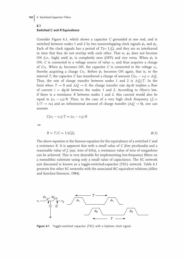
162 6 Switched-Capacitor Filters
6.1Switched C and R Equivalence
Consider Figure 6.1, which shows a capacitor C grounded at one end, and isswitched between nodes 1 and 2 by two nonoverlapping clock signals φ1 and φ2.Each of the clock signals has a period of T(= 1/fs), and they are so interleavedin time that they do not overlap with each other. That is, φ2 does not becomeON (i.e., high) until φ1 is completely zero (OFF) and vice versa. When φ1 isON, C is connected to a voltage source of value v1 and thus acquires a chargeof Cv1. When φ2 becomes ON, the capacitor C is connected to the voltage v2,thereby acquiring a charge Cv2. Before φ1 becomes ON again, that is, in theinterval T, the capacitor C has transferred a charge of amount C(v1 − v2) = Q .Thus, the rate of charge transfer between nodes 1 and 2 is Q/T . In thelimit when T → 0 and Q → 0, the charge transfer rate dq/dt implies a flowof current i = dq/dt between the nodes 1 and 2. According to Ohm’s law,if there is a resistance R between nodes 1 and 2, this current would also beequal to (v1 − v2)/R. Thus, in the case of a very high clock frequency ( fs =1/T → ∞) and an infinitesimal amount of charge transfer (Q → 0), one canassume
C(v2 − v1)/T = (v2 − v1)/R
or
R = T/C = 1/(Cfs) (6.1)
The above equation is the famous equation for the equivalence of a switched C anda resistance R. It is apparent that with a small value of C (few picofarads) and areasonable value of fs (say, tens of kHz), a resistance value of tens of megaohmscan be achieved. This is very desirable for implementing low-frequency filters ona monolithic substrate using only a small value of capacitance. The SC networkjust discussed is known as a toggle-switched-capacitor (TSC) network. Table 6.1presents few other SC networks with the associated RC equivalent relations (Allenand Sanchez-Sinencio, 1984).
1 2f1
f1 f2f1
f2
T
T
f2
C
Figure 6.1 Toggle-switched capacitor (TSC) with a biphase clock signal.

6.2 Discrete-Time and Frequency Domain Characterization 163
Table 6.1 A few SC networks with associated RC equivalences.
Designated name SC network RC equivalencerelation
A Series-switched C
C
+
−
+
−
n1 n2
f1
f2 R = T/C
B Series-shunt switched C +
−
n1C1
f1 f2
C2
+
−
n2R = T/(C1 + C2)
C Toggle-switched Cn2
C
n1
f1 f2
R = T/2C
D Differential toggle-switched C n1
f2
f2
f1
C
f1
n2 R = T/4C
6.2Discrete-Time and Frequency Domain Characterization
The development above has been carried out in an approximate way, assuming thatthe clock frequency is very high compared to the signal frequencies. In reality, thisis not true and, hence, it is necessary to use accurate timing information to accountfor the transfer of charge between two nodes by an SC connected between thesenodes. The pertinent system of equations then becomes discrete-time equations,instead of a continuous-time one. The associated frequency domain characterizationis termed discrete or sampled-data frequency domain characterization. Instead of theconventional continuous frequency variable s = jω, we have to use the sampled-datafrequency variable z = exp( jT), where F(z) is the z-transform of f (nT) and
is the sampled-data analog of the continuous-time-domain angular frequencyω. Depending upon the way the SC network is operated, distinct relationshipsbetween the s and the z variables arise. This, thus, leads to several possible

164 6 Switched-Capacitor Filters
transformation relationships between the continuous domain frequency variableand the sampled-data domain frequency variable. Several of these are illustrated inthe section to follow, by considering the SC equivalent to a continuous-time-domainRC integrator.
6.2.1SC Integrators: s ↔ z Transformations
Consider Figure 6.2. In Figure 6.2a, we show an active-RC integrator using an OA;in Figure 6.2b, a corresponding SC integrator with the resistance replaced by a TSCresistor is shown. For the RC integrator, the voltage transfer function is uniqueand is given by
T(s) = Vo(s)
Vi(s)= − 1
sRC(6.2)
The clock signal (Figure 6.2c) φ1 goes ON at instants of time (n − 1)T , nT , . . . ,and the clock signal φ2 goes ON at instants of (n − 3/2)T , (n − 1/2)T , . . . , so thateach clock signal has a period of T. They do not overlap each other. For sampledata operation, the sampling instants are considered to be coincident with theinstants (n − 3/2)T , (n − 1)T , (n − 1/2)T , . . . , and so on. It has to be understoodthat, during the ON period of each clock phase, the network has a specific topology(i.e., interconnection pattern) and the topology changes as the clock phase alternatesbetween φ1 and φ2. Thus, Figure 6.3a shows the topology of the network when clock
(a)
+
−R
C
i
o
(b)
C
C1 +
−
f1 f2
(c)
n −1
n − 3/2 n −1/2 n + 1/2
n
T
T
t /T →
f1
f2
i
o
Figure 6.2 (a) Active-RC integrator, (b) TSC integrator, and(c) nonoverlapping clock signals.
C
C1 +
−
o
i
C
C1 +
−
(a) (b)
o
Figure 6.3 Configuration of the TSC integrator when(a) clock signal φ1 is ON and (b) clock signal φ2 is ON.

6.2 Discrete-Time and Frequency Domain Characterization 165
φ1 is ON, say at t/T = (n − 1), that is, t = (n − 1)T. At this time, C1 has a voltagevi(n − 1) across it, while C has a voltage vo(n − 1) across it. Note that, for simplicity,we are using (n), (n − 1), . . . , to imply the time instants nT, (n − 1)T , . . . , andso on. The voltage vo(n − 1) is, however, the sampled and held version of voltagevo(n − 3/2), since it was at this instant of time (i.e., t = (n − 3/2)T) that C happenedto be connected to C1 and was subjected to the charge redistribution operation withC1. Therefore, vo(n − 3/2)T is like an initial value that is held until t = (n − 1)T.
Similarly, at t = (n − 1/2)T , when φ2 goes ON, the network topology is as shownin Figure 6.3b. The capacitor C1, being across the input terminals of the OA, isvirtually shorted and hence the charge across it becomes zero. The charge on Cis now Cvo(n − 1/2). At the instant t = nT , the scenario at t = (n − 1)T repeats,because the time interval is the same as the periodic interval T of the clocksequence. Thus, over one periodic interval of time T, the following changes occurin the charges held on the capacitors C and C1.
For C,
QC = QC(n − 1/2) − QC(n − 1) = Cvo(n − 1/2) − Cvo(n − 1) (6.3a)
For C1,
QC1 = QC1 (n − 1/2) − QC1 (n − 1) = 0 − C1vi(n − 1) (6.3b)
According to the principle of charge conservation, QC = QC1 . Then, fromEqs. (6.3a) and (6.3b), we can write
Cvo(n − 1/2) − Cvo(n − 1) = 0 − C1vi(n − 1) (6.4)
The above is an equation in the discrete-time domain. To move to thediscrete-frequency domain, we have to apply the z-transform to both sides of theequation. We must also remember that we are dealing here with the z-transformsfor two distinct sampling sequences. One is due to the clock φ1 and the other isdue to the clock φ2 – both having an identical sampling period T. Assigning thesuperscript (1) for the z-transform corresponding to φ1 and the superscript (2) forthe z-transform corresponding to φ2 , we write, from Eq. (6.4):
C[Vo(z)
](2)z−1/2 − C
[Vo(z)
](1)z−1 = −C1
[Vi(z)
](1)z−1 (6.5)
In the above, we have used the convention that z[v(nT)] = V(z), where z[.] implies‘‘the z-transform of ’’ [.]. Since, however, we have discussed that vo(n − 1) =vo(n − 3/2), by taking the z-transform, we can write[
Vo(z)](1)
z−1 = [Vo(z)
](2)z−3/2, that is,
[Vo(z)
](1) = z−1/2 [Vo(z)
](2)(6.6)
Equation (6.6) is a special relationship between [Vo(z)](1) and [Vo(z)](2) that holdsbecause of the sample-and-hold relation that is satisfied by the voltage vo(nT). Thiskind of relationship may not necessarily hold for Vi, unless we ascribe a similarsample-and-hold condition for the signal vi(nT).
Figures 6.2 and 6.3 indicate that the output vo changes only during the phase φ2,that is, when C is switched ON to the inverting input terminal of the OA. Therefore,

166 6 Switched-Capacitor Filters
we shall maintain Vo(z)(2) as the significant output variable. Then, we rewrite Eq.(6.5), after using the relation in Eq. (6.6):
CVo(z)(2)z−1/2 − CVo(z)(2)z−3/2 = −C1Vi(z)(1)z−1
Dividing out by z−1/2, we get
CVo(z)(2) − CVo(z)(2)z−1 = −C1Vi(z)(1)z−1/2 (6.7)
Now taking the ratio, we get the z-domain transfer function for (1,2) phasecombination (ignoring the argument z for simplicity):
V (2)o
V (1)i
= H(1,2) = −C1
C
z−1/2
1 − z−1(6.8a)
An alternative transfer function could be defined by considering the (1,1) phasegroup, that is,
V (1)o
V (1)i
= H(1,1) = −C1
C
z−1
1 − z−1(6.8b)
An interesting matter is immediately apparent, that is, we have been able to definetwo distinct z-domain transfer functions for the SC integrator network, while thereis only one unique transfer function for the associated RC integrator, as given byEq. (6.2). Using the equivalence R → T/C1 for the TSC-R equivalence in Eq. (6.8a),we get
H(1,2) = − T
RCz−1/2
1 − z−1(6.9)
We can draw an interesting correspondence between the continuous-time-domain frequency variable s and the sampled-data domain frequency variable z bycomparing Eq. (6.2) with Eq. (6.9). Thus,
T(s) ↔ H(1,2)
leads to
1sRC
↔ T
RC
z−1/2
1 − z−1
That is,
s ↔ 1
T
1 − z−1
z− 12
or
s ↔ 1
T
(z
12 − z− 1
2
)(6.10)
The above represents a popular s ↔ z transformation known as lossless digi-tal integrator (LDI) transformation. One can appreciate the implication of thistransformation by conceptualizing that, if an integrator-based RC-active filter isconverted to an SC filter with the RC integrators (as in Figure 6.2a) replaced byTSC-C integrators (as in Figure 6.2b), then the transfer function of the SC filter

6.2 Discrete-Time and Frequency Domain Characterization 167
in z-domain can be written down from the transfer function of the RC-activefilter simply by replacing ‘‘s’’ by the function of ‘‘z,’’ as given by the s ↔ ztransformation relation Eq. (6.10). It must also be understood that the output ofeach SC integrator in the filter must be sampled and transferred to the followingstage in the filter, during the clock phase φ2, so that the transformation in Eq.(6.10) is applicable. If, on the other hand, the output of each SC integrator inthe filter is sampled during clock phase φ1, the pertinent transformation willbe s ↔ 1
T (z − 1). One can derive this transformation relation by comparing thetransfer function of Eq. (6.2) with the z-domain transfer function given by Eq.(6.8b). Two other important s ↔ z transformations can be derived by consideringan alternative implementation of a resistance by an SC network, while replacing anRC integrator with an SC integrator. Table 5.2 presents the various s ↔ z transfor-mations. For more details regarding the various transformations, one may refer toMohan, Ramachandran, and Swamy (1982, 1995) and Allen and Sanchez-Sinencio(1984).
6.2.2Frequency Domain Characteristics of Sampled-Data Transfer Function
By now, it is clear that a given continuous-time transfer function H(s), when imple-mented using SC network, produces a transfer function H(z) in the discrete-timedomain. Corresponding to a given H(s), there could be more than one possibleH(z) because of the presence of more than one clock signal in the SC network.For frequency domain characterization of H(z), we use the relation z = exp( jT),where is the sampled-data angular frequency. This is identical with the real phys-ical frequency used to test and simulate a sampled-data system. Since exp( jT)is a periodic function, it is obvious that H(z) will be a periodic function. This isan important distinction between the continuous-time frequency domain transferfunction H(s) and the sampled-data (i.e., discrete-time) frequency domain transferfunction H(z). One may visualize the situation as though the given H(s), whenimplemented as an SC filter function, causes H(s) to be modulated in frequencydomain (multiplied in time domain) by the clock frequency fs = 1/T of the clocksignals. Thus, corresponding to an LP |H( jω)|, we get a periodic train for |H(e jT )|,which will consist of lobes of |H( jω)| around zero frequency (i.e., DC) and around±2π fs, ±4π fs, . . . , ±2nπ fs. This is illustrated in Figure 6.4, where fs = 1/T .
H(jw)
wBw → ← −ΩT
4p −wBΩ →wB
H(jw) ↔ H(e j ΩT)
H(e j ΩT)s ↔ z
−T2p−
T2p
T4p
Figure 6.4 Sampling operation on |H( jω)| and the sampled spectrum |H(e jT )|.

168 6 Switched-Capacitor Filters
From the above, it is clear that in order for the adjacent response lobes in |H(e jT )|not to overlap (i.e., alias) with each other, one must maintain ωs = 2π fs ≥ 2ωB,where ωB is the significant bandwidth in the continuous-time-domain transferfunction H(s). This observation is consistent with the Nyquist rate sampling, asused in communication systems. In practice, a value of ωs ≥ 8ωB is employed.When fs is fixed by other system constraints, the bandwidth of the incoming signalis restricted to a value less than fs/2 by an antialiasing filter. This filter could bea simple passive-RC section. The band-limited signal is then subjected to the SCfilter system. In cases where a continuous-time response is required, the SC filteroutput is smoothened by a continuous-time smoothing or reconstruction filter.The reconstruction filter must reject all the lobes in |H(e jT )| beyond the frequencyof ωB. The system diagram is illustrated in Figure 6.5a. Since the antialiasing andreconstruction filters are simple RC networks, one can consider Figure 6.5b to getan idea of the frequency response characteristics of such filters. The passband ofthese filters must cover frequencies up to ωB. The transition band of the filter willdepend upon the separation of ωs and ωB, specifically on ωs − ωB. As Figure 6.5bindicates, one must have the TB (≥ ωs − ωB) − ωB = ωs − 2ωB to avoid aliasingand to obtain a faithful reconstruction of the signal processed by the SC filtersystem.
Apart from the periodic characteristic of H(z), there is another interesting char-acteristic of the sampled-data frequency variable z = exp ( jT). As the frequencyvaries over the range −∝≤ ≤∝, z moves along the periphery of a circle of unitradius. Considering the complex frequency variable s = σ + jω and z = exp(sT),the left-hand side (LHS) of the s-plane (i.e., σ < 0) is mapped into the interior ofthe circle of unit radius in the z-plane (i.e., |z| < 1) and the RHS of the s-plane(i.e., σ > 0) is mapped to the exterior of the unit circle in the z-plane (i.e., |z| > 1).The jω axis in the s-domain is mapped on to the periphery of the unit circle in thez-domain (i.e., |z| = 1).
The various s ↔ z transformations shown in Table 6.2 lead to similar charac-teristics related to H(z) as discussed above. But the accuracy with which the H(z)associated with a specific H(s) matches the given H(s) and varies with the type ofs ↔ z transformations chosen. The reason is the exponential relationship betweenthe continuous-time and the sampled-data frequency variables, that is, s and z. Usu-ally, an optimization algorithm may be required to improve the matching betweena given analog H(s) and the associated sampled-data H(z), which results afterapplying a specific s ↔ z transformation. Synthesizing the H(z) corresponding to
Antialiasingfilter SC filter Reconstruction
filterIn Out
fs
T ( jw)
wB ws
(a) (b)0−ws +wB −wB −wB↑
TB
Figure 6.5 (a) Use of switched-capacitor filters in a prac-tical system. (b) Frequency response characteristics of theantialiasing and reconstruction filters.

6.3 Bilinear s ↔ z Transformation 169
Table 6.2 Some well-known s ↔ z transformations.
Transformation Various integrators
s ↔ 1
T(z1/2 − z−1/2) Lossless digital integrator (LDI)
s ↔ 1
T(z − 1) Forward difference integrator (FDI)
s ↔ 1
T(1 − z−1) Backward difference integrator (BDI)
s ↔ 2
T
1 − z−1
1 + z−1Bilinear integrator (BLI)
Table 6.3 Various steps in the design of an SC filter.
Given Ap, Aa, fp, and fa↓Synthesize H(s)↓Apply s ↔ z transformation (‘‘prewarp’’ if possible) – see Section 6.3↓Derive the corresponding H(z)↓Implement H(z) using SC and OA
an SC filter needs the application of one of the s ↔ z transformation relationsto a known H(s), which is derived from the basic specifications for the filter, asalready discussed in Chapter 3. A flow chart regarding this procedure is shown inTable 6.3.
6.3Bilinear s ↔ z Transformation
Of the several transformations, the BLT
s ↔ 2
T
1 − z−1
1 + z−1(6.11)
is very popular because the entire analog frequency range of zero to infinity istransformed to a range of zero to π/T in the sampled-data frequency. This can beverified by putting z = exp( jT) in Eq. (6.11) to get
ω = 2
Ttan
T
2(6.12)

170 6 Switched-Capacitor Filters
wI
w or Ω →Ω I
Mag
nitu
de→
H(jw)
H(e j ΩT)
Figure 6.6 Effect of warping due to bilineartransformation on H(s).
Thus, when ω = 0, = 0, but when ω = ∞, one gets tan T2 = ∞; hence,
= π/T . This also implies that the response H(z) will be somewhat squeezedin the sampled-data frequency domain, if H(z) were derived from H(s) by theapplication of the BLT. This is known as the warping effect of the BLT. Thus, agiven frequency ωI in the analog domain is squeezed to I in the sampled-datadomain with I < ωI. Actually, H(z)|z=exp( jIT) becomes equal to H(s)|s=jωI . Thisis easily illustrated by Figure 6.6.
This warping effect can be compensated by what is known as prewarping thefrequencies of the analog filter. Thus, if ωI is a significant frequency (for example,the passband edge frequency) in H(s), one can rewrite H(s) with ωI replaced by theprewarped frequency ωI, given by
ωI = 2
Ttan
(ωIT
2
)(6.13)
The corresponding transfer function may be labeled as H(s) and is known as theprewarped analog transfer function. After application of the BLT to this new transferfunction H(s), one gets H(z). The frequency I in H(z) will then, by virtue of theBLT,
I = 2
Ttan−1
(ωIT
2
)= 2
Ttan−1
(T
2
2
Ttan
[ωIT
2
])= ωI (6.14)
which is same as the original frequency of interest. Thus, by prewarping, the effectof distortion due to the BLT is eliminated at the frequency ωI. If there is morethan one critical frequency in H(s) (for example, the passband edge frequency ωc
and the stopband edge frequency ωa), then the process of prewarping is appliedto all these frequencies before obtaining the prewarped analog transfer functionH(s). Table 6.4 presents the set of biquadratic transfer function expressions in thesampled-data domain associated with the corresponding analog transfer functionexpressions (Raut, 1984), when the BLT is used.
Example 6.1. Consider the second-order BP analog transfer function given
by H(s) = 2027.9s
s2 + 641.28s + 1.0528 × 10⁸. Obtain the corresponding sampled-data
transfer function H(z) using the BLT. The clock frequency is 8 kHz.From the given H(s), one can calculate the following:
ωp =√
1.0528 × 108 = 1.026 × 10⁴, ω p/Qp = 641.28,
Q p = 16, HBP = 2027.9/641.28 = 3.162 → 10 dB

6.3 Bilinear s ↔ z Transformation 171
Table 6.4 Sampled-data filter functions associated with stan-dard biquadratic filter functions when the BLT is used.
Filter type Analog transfer function Sample-data transfer function
H(s) = N(s)F1(s)
H(z) = hD1 + a1Nz−1 + a2Nz−2
1 − a1Dz−1 + a2Dz−2
hD a1N a2N
LP HLPω2p/F1 HLPω2
p/F2 2 1
HP HHPs2/F1 HHPa2/F2 –2 1
BP HBP(ωp/Q p)s/F1 HBP(ωp/Q p)a/F2 0 –1
AP HAP[F1 − 2(ωp/Q p)s]/F1 HAPa2D −a1D/a2D 1/a2D
Notch HN (s2 + ω2n)/F1 HN (a2 + ω2
n)/F2 −2(a2 − ω2n)/(a2 + ω2
n) 1
Note: a = 2/T , ωp = a tan(ωp/a), ωn = a tan(ωn/a).F1 = s2 + (ωp/Qp)s + ω2
p , F2 = a2 + (ωp/Qp)a + ω2p .
a1D = 2(a2 − ω2p)/F2, a2D = [a2 − (ωp/Qp)a + ω2
p ]/F2.
Since fs = 8 kHz, T = 125 µs. Hence,
ωp = 2fs tan(ωp/2fs) = 1.1944 × 10⁴, ωp/Q p = 746.488
Thus, the prewarped analog transfer function will be
H(s) = HBP(ωp/Qp)s
s2 + (ωp/Qp)s + ω2p
= 3.162 × 746.488s
s2 + 746.488s + 1.42659 × 10⁸
One can now apply the BL s ↔ z transformation to derive the various coefficientsassociated with the sampled-data transfer function H(z). Thus,
hD = 9.192 × 10⁻², a1D = 0.5521, a2D = 0.9418
Therefore,
H(z) = 9.192 × 10⁻²(1 − z−2)1 − 0.5521z−1 + 0.9418z−2
(6.15)
It may be remarked that one could skip the intermediate step of writing down H(s)and get to H(z) directly by applying the relations given in Table 6.4.
To calculate the magnitude response, one has to substitute z = exp( jT) andassign different values to the frequency variable . For the problem on hand,T = 125 µs. The curves in Figure 6.7a depict the magnitude responses correspond-ing to H( jω) and H(e jT ), as obtained by the MATLAB program. The listing ofthe program is given in Program 6.1. The differences between |H( jω)| (solid line)and |H(e jT )| (dotted line) at frequencies other than ωp is due to the fact that theprewarping has been used at only one frequency, that is, at ωp. If one would ratherchoose the −3 dB frequencies of the response function and apply prewarping tothese two frequencies, the derived H(e jT ) would show a better matching with thegiven H( jω).

172 6 Switched-Capacitor Filters
3.5
0.12
0.1
0.08
0.06
0.04
0.02
0
−0.02
3
2.5
2
1.5Mag
nitu
deE
rror
1
0.5
00 2000 4000 6000 8000 10000 12000 14000 16000
Frequency (Hz)
0 2000 4000 6000 8000 10000 12000 14000 16000
Frequency (Hz)
(a)
(b)
er 1
er 2
H(jw)
H(e j ΩT)
Figure 6.7 Illustration of the effects of prewarping:(a) applied to the center frequency and (b) applied to thetwo-band edge frequencies of a band-pass filter.
To accomplish the above task, one first finds out that the bandwidth of the BP filteris ωp/Qp = 641.28 rad s−1. If ωh and ωl are the higher and lower −3 dB frequencies ofthe BP filter, then ωh − ωl = bandwidth = 641.28. The geometric symmetry of a BPfilter dictates that ωh × ωl = ωp
2 = 1.0528 × 10⁸. These give (solving the quadraticequation), ωh = 1.059 × 10⁴ and ωl = 9.945 × 10³. We can now apply prewarpingto these two frequencies. We then get ωh = 1.246 × 10⁴, ωl = 1.146 × 10⁴, thereby

6.4 Parasitic-Insensitive Structures 173
giving the prewarped bandwidth ωh − ωl = 9.995 × 10². Remembering that theprewarped resonant frequency is now given by ω2
p = ωh × ωl = 1.428 × 10⁸, the
prewarped transfer function will become H′(s) = 3161ss2+999.5s+1.428×10⁸ . On application
of the BLT, the sampled-data transfer function will be
H′(z) = 0.1219(1 − z−2)
1 − 0.5455z−1 + 0.9229z−2(6.16)
The curves in Figure 6.7b show the errors er1 = |H( jω)| − |H(e jT )| (the curvewith +++) and er2 = |H( jω)| − |H′(e jT )| (the solid line curve) as a function offrequency. The error in |H′(e jT )| relative to |H( jω)| is less than that with |H(e jT )|,as expected.
Program 6.1 MATLAB code for the magnitude responses of H( jω) and H(e jT ), andthe error magnitudes
%sampled-data filterFs=8e3;% analog filter responsea=[1 641.28 1.0528e8];b=[0 2027.9 0];f=linspace(150,2500,901);w=2*pi*f;h=freqs(b,a,w);mag1=abs(h);b=[9.192e-2 0 -9.192e-2];a=[1 -.552 0.9418];f=linspace(150,2500,901);w=2*pi*f;h=freqz(b,a,f,Fs);mag2=abs(h);b=[.1219 0 -.1219];a=[1 -.5455 0.9229];f=linspace(150,2500,901);w=2*pi*f;h=freqz(b,a,f,Fs);mag3=abs(h);er1=(mag1-mag2)/3.316;er2=(mag1-mag3)/3.316;%plot(w,mag1,’w-’,w,mag2,’w.’)plot(w,er1,’w+’,w,er2,’w-’)gridxlabel(’Freq.(Hz)-->’);%ylabel(’Magnitude |H(s)|--, |H(z)|..’);ylabel(’Error er1++, er2--’);end
6.4Parasitic-Insensitive Structures
It has already been mentioned that SC filters received considerable attentionbecause of the potential for fabrication as an IC. In this respect, however, a problem

174 6 Switched-Capacitor Filters
arises because of the presence of unwanted capacitances that are invariably presentin an IC structure. Virtually, any two distinct semiconductor layers will have acapacitance associated with the junction between them. This is true both for theMOS transistors that are used as switches in an SC network, as well as for theMOS capacitors that have additional layers of semiconductors as part of the ICtechnological process flow. One can consider Figures 6.8a and 6.8b which depictthe typical interlayer capacitances that arise in a MOS transistor and in a double-polyMOS capacitor (Schaumann, Ghausi, and Laker, 1990) respectively.
For the MOS transistor in Figure 6.8a, the bulk (substrate) is usually connectedto a fixed DC potential so that this node can be considered to be signal ground (ACground). The capacitors Cbd1, Cbc1, and Cbs1 can be lumped as parasitic capacitancesCSW at the drain and source ends as shown on the RHS of Figure 6.8a. Theparasitic capacitances (Cgdo, Cgc , Cgso, and Cgb) from the gate to drain, to channel, tosource, and to bulk nodes are responsible for clock feedthrough effects. Similarly,in Figure 6.8b, the actual design capacitance CR between the two poly layers isattended by parasitic capacitances such as Cj, Cm from the top plate, and Cb fromthe bottom plate. Because of closer proximity to signal ground (i.e., fixed DCpotential), Cb has a higher value than Cj or Cm. The equivalent circuit on the RHS
Connected to DC(AC ground)
Bulk (substrate)
Cbd1
Cbc1
Cgc
Rd
Cgb
Cgso
Channel
Clock
GateOxideCgdoDrain
Signalin
Signalout Clock
G
SCSWCSW
D
Source
Cbs1
Rs
(a)
(b)
(i) Top plateMetal
Poly2
Poly1
Thinox
Thick oxide
n− substrate
VDD (AC ground)
Cj
n+
CmCR
CbCb
(i)
(ii)Cm Cj
CR
VDD (AC ground)
Metal
Bottom plate (ii)
Figure 6.8 Parasitic capacitances in (a) an MOS transistor and (b) an MOS capacitor.

6.4 Parasitic-Insensitive Structures 175
OA
+
−
(i)(ii)
VDD (AC ground)
VDD (AC ground)
VDD (AC ground)
VDD (AC ground)
(a)
(b)
CSW
COACSW CSW
CSWCR 1
CR2 Cb
Ct
Cb
Ct = Cm + Cj
Vin
Vin
Vout
Vout
OA+
−CR 1
CR 2f1
f1 f2
f2
(a)
(b)
Figure 6.9 (a) A TSC integrator ignoring the parasitic ca-pacitances. (b) The TSC integrator including the parasiticcapacitances of the MOS switches and MOS capacitors.
of Figure 6.8b presents the situation for a design capacitance CR in a typical MOS(or CMOS) IC technology.
If we incorporate the above information in a TSC integrator (see Figure 6.9a whenno parasitic capacitances are assumed to be present), where a TSC of value CR1 isused to replace the resistance and CR2 is the integrating capacitor, the schematicincluding the parasitic capacitances will appear as shown in Figure 6.9b. In theschematic of Figure 6.9b, the switches are replaced with MOS transistors driven byappropriate clock signals (i.e., φ1 and φ2). Out of the several parasitic capacitances,those connected to a voltage source node (i.e., Vin, Vout) and those at the virtualground input node of the OA can be ignored for signal processing since theyeither instantly hold the signal voltages or are at zero signal potential. The parasiticcapacitances that are neither at a voltage source node nor at the virtual ground nodecontribute to the charge conservation equation (CCE) during the switching phasesφ1 and φ2. A more simplified schematic obtained by considering only the importantparasitic capacitances is shown in Figure 6.10. It is seen that the switch parasiticcapacitances CSW and the top-plate capacitance Ct of the MOS capacitance CR1
should be taken into consideration when writing the discrete-time equations suchas Eqs. (6.3) and (6.4). This does not pose any theoretical problem, but the practicalproblem is the uncertainty about the exact values of the parasitic capacitances.The values are dependent upon the actual value of the design capacitance as wellas on the layout of the transistors and the MOS capacitors. To save the space onthe substrate, the value of CR (see Figure 6.8b) should be limited to within 10 pF

176 6 Switched-Capacitor Filters
f1 f2
Vin
Vout
(a)(b)
CSW CSW
Ct = Cm + Cj
Ct
COA OA
+
−
CR1
CR2 Cb
(b)VDD (AC ground)
VDD (AC ground)
VDD (AC ground)
VDD (AC ground)
Figure 6.10 Simplified schematic of the TSC integra-tor of Figure 6.9b, showing only the important parasiticcapacitances.
and an uncertain value of the parasitic capacitance, which could in some cases beas large as 80% of the design capacitance, makes accurate theoretical calculationrather difficult. This difficulty is overcome by the use of PI–SC networks thatare described below (Gregorian and Nicholson, 1979; Mohan, Ramachandran, andSwamy 1982; Schaumann, Ghausi, and Laker, 1990).
6.4.1Parasitic-Insensitive-SC Integrators
In PI-SC integrators, the parasitic capacitance is discharged to signal ground bythe appropriate clock signal, before the design capacitance (i.e., which is replacingthe resistance) acquires a new charge or shares its charge with another capacitor.Thus, while the parasitic capacitance is present physically, it does not contributetoward the CCE.
In the following, the switching symbol (wherever used) implies the presenceof an MOS transistor operated by (i.e., driven at the gate terminal) a clock signalφi(i = 1, 2).
6.4.1.1 Lossless IntegratorsFigure 6.11a shows a PI-SC integrator, known as the inverting PI-SC integrator.Prior to clock phase φ1, the two plates of C1 are discharged to signal ground, therebyremoving all the charges on the parasitic capacitances Cp1 and Cp2. Figure 6.11bshows a PI-SC integrator known as the noninverting PI-SC integrator.
It may be seen that, in Figure 6.11b, the left-side plate of C2 is charged during φ2,while the right-side plate and the parasitic Cp2 are discharged to ground. During φ1,a reverse operation takes place with C2, since the left-side plate (and the parasiticCp1) is now grounded, while the right-side plate gets connected to the input of theOA. Because of this signal reversal, accomplished by reversing the plates of C2, thesystem produces a noninverting mode of operation.

6.5 Analysis of SC Networks Using PI-SC Integrators 177
in
out
C1
Co
cp1
OA+
−
cp2
f1f1
f2 f2
(a)
C3
C1
C2
f1
f1
f2 f2
f1
f2 f2
f1
OA−
+
(c)
C3
C1
C2
f2
f1
f2 f1
f2
f1 f1
f2
OA−
+
(d)
Co
C2
cp1
OA+
−
cp2
f2f1
f1 f2
(b)
in
inin
out
outout
Figure 6.11 Parasitic-insensitive (PI) integrators: (a) loss-less inverting, (b) lossless noninverting, (c) lossy inverting,and (d) lossy noninverting.
6.4.1.2 Lossy IntegratorsFigures 6.11c and 6.11d show two lossy integrator configurations using PI-switching schemes. Basically, a lossy integrator is formed by connecting a PI-SCresistance across the integrating capacitor C2. Both lossless and lossy integratorsare important for active filter realizations. The inverting and noninverting lossyintegrator structures are depicted in Figures 6.11c and 6.11d, respectively. Thecapacitor C3 affords the lossy integrator operation.
In the following, we discuss the technique of analysis of PI-SC integrators in amodular way. The analysis can be used to derive the transfer functions of the PI-SCintegrators, and can be easily extended to more complex SC networks involving PIfeatures.
6.5Analysis of SC Networks Using PI-SC Integrators
6.5.1Lossless and Lossy Integrators
6.5.1.1 Inverting Lossless IntegratorConsider Figure 6.12a, which shows a PI-SC integrator with an input signal vin.The path for vin is the inverting mode of operation. The signal is switched to the OAinput only during the ON phase of the clock φ1. When the clock signals are eitherON or OFF, the respective network topologies are linear time invariant; hence, the

178 6 Switched-Capacitor Filters
in
C1
Co
OA−
+
f1 f1
f2 f2
(a)
C2
Co
OA−
+
f2 f1
f1 f2
T
T
f1
nn −1
n − 1/2n − 3/2
t /T →
n + 1/2
f2
T
T
f1
nn − 1
n − 1/2n − 3/2
t /T →
n + 1/2
f2
(b)
inout
out
Figure 6.12 (a) Inverting lossless PI-integrator and (b) non-inverting lossless PI-integrator, along with the clock signals.
principle of superposition holds. Considering the discrete-time equation for thesignals vin and vout, the CCE gives
0 − C1vin(n − 1) = Covout(n − 1) − Covout(n − 3/2)
Using the condition vout(n − 3/2) = vout(n − 2), taking z-transform and simplify-ing, one arrives at
V(1)out = −C1
Co
1
1 − z−1V
(1)in (6.17)
where V(1)out and V
(1)in are the z-transforms of vout(n) and vin(n) respectively due
to the clock signal φ1. One may note the appearance of the negative sign infront of (C1/Co) on the RHS of Eq. (6.17) because of the inverting integrationoperation. Since vin is processed through C1 without any intermediate delay, andis connected to the inverting input of the OA, a sign inversion is inevitable. Theterm (1 − z−1) in the denominator of the RHS of Eq. (6.17) appears because ofintegration by sample-and-hold operation over one full clock period T. Because ofthe sample-and-hold operation, we can further derive
V (2)out = z− 1
2 V (1)out (6.18)
clock φ2 being nominally one-half period delayed relative to clock φ1. It should benoted that since Co receives a new packet of charge each time the clock φ1 comesON, the signal vout is available in reality during phase 1. Hence, we use V (1)
out as theprimary variable in Eq. (6.17).
If the clock signals in Figure 6.12a are interchanged, we can similarly obtain
V (2)out = −C1
Co
1
1 − z−1V (2)
in (6.19)

6.5 Analysis of SC Networks Using PI-SC Integrators 179
and
V (1)out = z− 1
2 V (2)out (6.20)
6.5.1.2 Noninverting Lossless IntegratorConsider Figure 6.12b, with an input signal vin. Because of the reversal of the platesof C2 between clock phases, the CCE becomes
0 − (−C2vin(n − 3/2)) = Co[vout(n − 1) − vout(n − 3/2)
]But vout(n − 3/2) is the same as vout(n − 2) sampled to and held on Co. In the
z-transform domain, this implies z− 32 V (2)
out = z−2V (1)out, where V (1)
out is the z-transformof vout(n) for the clock signal φ1, and V (2)
out is the z-transform of vout(n) owing toclock signal φ2. Taking z-transform on both sides and relating vout(n − 3/2) withvout(n − 2) as mentioned above, we get
C2z−3/2V (2)in = Coz−1V (1)
out − Coz−3/2V (2)out = Coz−1V (1)
out − Coz−2V (1)out
where V (2)in is the z-transform of vin(n) due to the clock signal φ2. Dividing both
sides by z−1 and simplifying, one gets
V (1)out = C2
Co
z−1/2
1 − z−1V (2)
in (6.21)
One may note that since the signal vin in this case is processed for noninvertingintegration, there is no negative sign in front of (C2/Co) on the RHS of Eq. (6.21).Further, since vin is held on C2 during the ON period of φ2 and switched on tothe input of the OA during the ON period of φ1, that is, an interval of T/2 later,the term z−1/2 appears in the numerator of the RHS of Eq. (6.21). This signifiesone-half period delay in the signal path. The denominator (1 − z−1) in Eq. (6.21)is a characteristic of the integration and appears in view of the sample-and-holdoperation over a full period T by the integrating capacitor Co. Because of the timerelationship between φ1, and φ2, we can write as before,
V (2)out = z− 1
2 V (1)out (6.22)
If the clock signals in Figure 6.12b are interchanged, we can similarly obtain
V (2)out = C2
Co
z− 12
1 − z−1V (1)
in (6.23)
and
V(1)out = z− 1
2 V(2)out (6.24)
6.5.1.3 Inverting and Noninverting Lossless Integration CombinedConsider Figure 6.13a, where signal v1 is processed for inverting integration, whilesignal v2 is processed for noninverting integration. Equations (6.17) and (6.21) werederived assuming the presence of only one signal at a time. When both v1 and v2

180 6 Switched-Capacitor Filters
n −1
n − 1/2 n + 1/2n − 3/2
n
f1
f2
t /T →
T
T
n − 1
n − 1/2 n + 1/2n − 3/2
n
f1
f2
t /T →
T
T
1
2
o
f1
f2 f2
f2
f2
f1
f1
f1C1
OA
Co
C2
+
−
f2
f1 f1
f1
f1
f2
f2
f2C1
OA
Co
C2
−
+
(a)
(b)
2
1
o
Figure 6.13 Parasitic-insensitive (PI) inverting andnoninverting integrators combined: OA input connected tothe signal paths during (a) clock phase φ1 and (b) clockphase φ2.
are operating simultaneously, one can invoke the superposition principle of lineartime-invariant networks and write
V (1)o = C2
Co
z−1/2
1 − z−1V (2)
2 − C1
Co
1
1 − z−1V (1)
1 (6.25)
In the above, V (y)x (x = 1, 2 and y = 1, 2) represent the z-transformed variables
pertaining to the signals vx (x = 1, 2) due to the two clock signals φ1 and φ2.Equation (6.25) represents the z-transformed output signal, when two signals v1
and v2 are fed to the OA input. Notice that, although the two signals are processedby the clock signals in different ways, they are connected to the input of the OA atthe same time (i.e., clock phase φ1). Since the signals are switched on to the OAinput during clock φ1, the significant output signal Vo is labeled with (1) as thesuperscript.
If the clock phases in the paths for v1 and v2 are switched around (see Figure 6.13b)with the OA input being connected to the signal paths during the clock phase φ2,we could similarly derive
V (2)o = C2
Co
z−1/2
1 − z−1V (1)
2 − C1
Co
1
1 − z−1V (2)
1 (6.26)
Note that, since now the signals are switched to the input of the OA duringthe clock signal φ2, the significant signal at the output is recognized as V
(2)o .
The reader is advised to practice writing down similar equations with othercombinations of clock phasing and signal positioning. It is obvious that the

6.5 Analysis of SC Networks Using PI-SC Integrators 181
above technique can be extended easily to cases with three or more input signalpaths.
6.5.1.4 Lossy PI-SC IntegratorReferring to Figure 6.11c, which depicts an inverting lossy integrator, we canvisualize that the signals vin and vout are switched to the OA input via the PI-SCelements C1, and C3. We can thus use Eq. (6.17), once for V (1)
in , and then for V (1)out,
followed by superposition. Hence, we get
V (1)out = −C1
C2
1
1 − z−1V (1)
in − C3
C2
1
1 − z−1V (1)
out (6.27)
The above equation leads to the transfer function
V (1)out
V (1)in
= −C1/(C2 + C3)
1 − C2z−1/(C2 + C3)(6.28)
The above is an inverting lossy integrator transfer function.Now, for the circuit of Figure 6.11d, note that vin is sampled in during φ1 but
applied to the OA input during φ2, with a phase reversal across the capacitor C1.Therefore, we can use Eq. (6.23) for V (1)
in . Similarly, we can use Eq. (6.19) for V (2)out.
Using superposition thereafter, we get
V(2)out = C1
C2
z− 12
1 − z−1V
(1)in − C3
C2
1
1 − z−1V
(2)out (6.29)
The above leads to the transfer function of the noninverting lossy integrator
V (2)out
V (1)in
= C1z−1/2/(C2 + C3)1 − C2z−1/(C2 + C3)
(6.30)
6.5.2Application of the Analysis Technique to a PI-SC Integrator-Based Second-Order Filter
Consider the Tow–Thomas (TT) biquad structure of Chapter 5 (Figure 5.16) withR4 = R/k, R3 = R2 = R, R1 = QR, and r1 = r2 = r. This leads to LP and BP filterrealizations using the RC-active filter configuration. The third OA in the TT networkserves to provide a gain of −1. This function can be easily obtained in the SC versionby employing a phase reversed SC network, as used in the noninverting PI-SCintegrator. This technique saves one OA in the SC version, which is presented inFigure 6.14. Our objective is to derive the z-domain transfer function V (2)
o2 / V (1)i ,
using the analysis technique discussed above.In order to apply the analysis technique presented in Section 6.5.1, one needs
to observe that, around the amplifier OA1, the (kC, C1) pair forms an invertingintegrator for the signal vi, the (C/Q, C1) pair forms an inverting integrator forvo1, and the (C, C1) pair forms a noninverting integrator for vo2. Similarly, for theamplifier OA2, the pair (C, C2) forms an inverting integrator for the signal vo1.

182 6 Switched-Capacitor Filters
vo1vo2
vi
C/Q
C
C
C1
OA1
f1
f1
f1 f1
f2f2
f1
f2
f2
f1
f2 f2
f1
f2 f2
f1C2
OA2+
−
+
−
kC
Figure 6.14 A second-order switched-capacitor filter using PI integrators.
With the above observations, one can write the following:
V (1)o1 = −C/Q
C1
1
1 − z−1V (1)
o1 − kC
C1
1
1 − z−1V (1)
in + C
C1
z−1/2
1 − z−1V (2)
o2
V (1)o1 = −C/Q
C1
11 − z−1
V (1)o1 − kC
C1
11 − z−1
V (1)in + C
C1
z−1/2
1 − z−1V (2)
o2
On rearranging and substituting A = C/QC1, B = kC/C1, and D = C/C1 in theabove equation, we get
V(1)o1
(1 + A
1 − z−1
)= − B
1 − z−1V
(1)in + D
z−1/2
1 − z−1V
(2)o2 (6.31)
For the subnetwork around OA2, we can similarly write
V (1)o2 = − C
C2
1
1 − z−1V (1)
o1 (6.32)
Writing E = C/C2, and noting that vo2(n − 1/2) = vo2(n − 1), in view of thesample-and-hold operation of C2, we get
V(1)o1 = −1 − z−1
EV
(1)o2 (6.33a)
and
V (2)o2 = z− 1
2 V (1)o2 (6.33b)
Substituting Eq. (6.33a,b) in Eq. (6.31), we have
V (1)o2
V (1)in
= BE
1 + A − (A − DE + 2)z−1 + z−2(6.34)

6.5 Analysis of SC Networks Using PI-SC Integrators 183
n − 1
n − 1/2 n + 1/2n − 3/2
n
f1
f2
t /T →
T
T
n − 1
n − 1/2 n + 1/2n − 3/2
n
f1
f2
t /T →
T
T
v1
v2
vo
f1
f2 f2
f2
f1
f2
f1
f1C1
OA
Co
C2
+
−
v1
v2
vo
f1
f2 f1
f2
f2
f1
f1
f2C1
OA
Co
C2
−
+
(a)
(b)
Figure 6.15 (a) PI inverting integrator having signalsswitched to the OA input during both the clock phases(φ1 and φ2). (b) PI noninverting integrator having signalsswitched to the OA input during both the clock phases(φ1 and φ2).
6.5.3Signals Switched to the Input of the OA during Both Phases of the Clock Signal
Consider Figure 6.15a, which represents this case for two input signals v1 and v2.One should note that under the present case the condition vo(n − 3/2) = vo(n − 2)cannot be applied any more. One can write the equations:
−C1v1(n − 1) = Covo(n − 1) − Covo(n − 3/2)
and
−C2v2(n − 1/2) = Covo(n − 1/2) − Covo(n − 1)
On taking the z-transforms and simplifying the above equations, we get
CoV (1)out − z−1/2CoV (2)
out = −C1V (1)1 (6.35a)
and
−z−1/2CoV (1)out + CoV (2)
out = −C2V (2)2 (6.35b)
One can put the above in the following compact form:[Co −z−1/2Co
−z−1/2Co Co
][V (1)
out
V (2)out
]= −
[C1V (1)
1
C2V (2)2
]
(6.36)

184 6 Switched-Capacitor Filters
In Figure 6.15a, the SC networks are configured to produce an inverting integrationoperation. If these are reconfigured to produce a noninverting integration operation(see Figure 6.15b), one could similarly derive
[ −z−1/2Co Co
Co −z−1/2Co
][V (1)
out
V(2)out
]= z−1/2
[C1V (1)
1
C2V(2)2
](6.37)
6.6Analysis of SC Networks Using Network Simulation Tools
When the network on hand is large and complex, hand analysis becomes verylaborious and prone to errors (Nelin, 1983). The analytical effort becomes evenmore complex for SC networks because of the presence of the clock phases,φ1 and φ2. If one models the MOS switches as voltage-controlled switches, itwill be possible to simulate a given SC network in the time domain, using thewell-known simulation programs such as SPICE, PSpice, HSPICE, and so on. Forfrequency domain analysis, however, this approach may be too time consumingsince measurements have to be taken at many frequencies. Assuming the switchesas ideal, however, leads to a simple method of modeling an SC network usingstandard components in the simulation routine. These components are ideal delaylines and voltage amplifiers. The procedure is discussed below.
If one reviews the various z-domain expressions discussed in Section 6.4,one can conclude that these expressions have the general form: Vout = kVi +Az−1/2Vo1 + Bz−1Vo2 + . . . , where k, A, and B are constants, Vi, Vo1, and Vo2 arethe z-transformed voltage signals, and z−1/2, z−1, . . . , imply delays by half-a-period,one full period, and so on. In simulation programs, such as SPICE, a voltage signalcan be modeled as it is, the constant coefficients can be modeled as amplification(or attenuation) factors, and the delays can be modeled by transmission lines witha fixed delay. The simulation of the operation of a filter can then be carried out inthe same way as simulating a system of equations in a state-variable filter usingmultipliers, adders, and integrators. The technique for the SC filter is illustrated inthe following.
6.6.1Use of VCVS and Transmission Line for Simulating an SC Filter
Consider the case of a PI inverting integrator transfer functionV
(1)out
V(1)i
= − C1Co
11−z−1 .
Writing the constant A = C1/ Co, we can write V (1)out = −AV (1)
i + z−1V (1)out. This is a
simple feedback equation and can be modeled easily by the block diagram shownin Figure 6.16. This block diagram can be emulated as in Figure 6.17 using idealvoltage amplifiers (i.e., VCVS) and ideal transmission lines, each with a delay ofone-half period of the clock signal.

6.6 Analysis of SC Networks Using Network Simulation Tools 185
(1)Vi
(1)Vo
-A
(Delay T )
z −1
× Σ
Figure 6.16 Block diagram realizing V(1)o =
−AV(1)i + z−1V(1)
o using basic delay, add, andmultiply operations.
Inverting summingamplifier
++
−−
+−
Vi(1)
+
−Vo
(1)
Vo(1)
Ro
AVi(1)
Vo(1) z −1/2
−Vo(1) z −1/2
− AVi(1) + z −1Vo
(1)
Vo(1)
−Vo(1) z −1
Feedback signal
Delay → T / 2 Delay → T / 2+ Ro+
−
Vd+
−
−
1kΩ
1kΩ
1kΩ
Delayed feedback signal
−+
−+
−+
+
−105 × Vd
+
−
1 × Vo1
Figure 6.17 Implementing the delay, add, and multiplyoperations in Figure 6.16, using standard circuit elementsin a SPICE program.
A systematic procedure to use this simulation technique will involve the followingsteps.
1) For the given SC filter, identify the SC subnetworks around each OA and writedown the expressions relating the output voltage variable to the input voltagevariable and the feedback voltage variables, in the form
Vout = kVi + Az−1/2Vo1 + Bz−1Vo2 + . . .
In case of feedback, one of the signals Vo1, Vo2, . . . , will be same as Vo.2) Use a half-period delay unit as the basic delay block and implement this with
a lossless transmission line having a delay of T/2 (T = full period) isolated bya unit gain voltage amplifier buffer (i.e., an ideal VCVS of gain 1 or −1). See,Figure 6.17, for example.
3) Implement ideal VCVS networks with gain values corresponding to the coeffi-cients in the equation derived in Step 1 above (i.e., k, A, B, . . .).
4) Connect the delay blocks and the VCVS blocks in conformity with the expres-sion derived in Step 1 above.

186 6 Switched-Capacitor Filters
5) Repeat Steps 1–4 for the subnetworks around each OA in the SC filter. Ensurethat the gain blocks have proper polarities with the gain so as to satisfy thesystem of equations correctly.
6) Write down the netlist file (or draw the schematic) for the entire networkobtained after Step 5.
7) Run the simulation in accordance with the guidelines of the simulationprogram (such as, PSpice) that is available.
Example 6.2. Consider the TT biquad shown in Figure 6.18a. With the valuesshown, the filter will have a center frequency of ωo = 1000 rad/s and a Qp of 5. AnSC implementation of the filter using a clock frequency of fs = 10 kHz is shownin Figure 6.18b. The netlist for simulating the response of the SC filter using thePspice program is given in Program 6.2. The simulated frequency response is
Program 6.2 PSpice code for simulation of the response of the SC filter ofFigure 6.18b
**SC filter simulation - TT-BIQUAD, ideal VCVS, switch.subckt del 1 2 4***clock period T=0.1mse1 3 0 1 2 1t1 3 0 4 0 zo=50 td=.05mrt 4 0 50.ends delvs 1 0 ac 1e2 2 0 1 0 .1r1 2 3 1kr2 15 3 1kr3 14 3 1kr4 10 3 1ke3 15 0 4 0 .02e4 14 0 12 0 -1e5 10 0 9 0 -.1e6 16 0 9 0 -1x1 4 0 11 delx2 11 0 12 delx3 7 0 8 delx4 8 0 9 delr5 3 4 1ke7 4 0 0 3 1e4ro1 4 0 1e8 5 0 4 0 0.1r6 5 6 1kr7 16 6 1kr8 6 7 1ke9 7 0 0 6 1e4ac dec 51 10 1kprint ac vm(4) vp(4)probeend

6.7 Design of SC Biquadratic Filters 187
C1C2
−
+
C
COA1 −
+OA2
C/Q
kCf1
f1f1
f2 f2
f1
f1
f1
f2f1
f2 f2 f2
f1
f2
vi
vo1vo2
f2
5K
+
−
+
−
+
V1
1K
1U
1U
1K
1K
1K
1KVs
V2
OA1 OA2
OA3(a)
(b)
Figure 6.18 (a) Tow–Thomas active-RC second-order filterand (b) a corresponding SC filter using PI switched-capacitorintegrators.
shown in Figure 6.19a. The time domain response at frequencies of 160, 100, and200 Hz are shown in Figures 6.19b to 6.19d.
6.7Design of SC Biquadratic Filters
In the ground-breaking era of SC filtering technique, the existing RC-activefilters were converted to active SC filters simply by using capacitors equiva-lent to the resistors in the RC structures in accordance with the ideal relationC = 1/Rfs, where fs is the sampling clock frequency. However, with the knowl-edge of PI-SC structures and the requirement of using z-transform techniquesfor accurate prediction of the behavior of the SC filters, the design techniquesleaned more toward realizing a given z-domain transfer function. Thus, in-stead of designing an SC filter equivalent to a parent active-RC filter, PI-SCnetworks and OAs were interconnected in special ways to realize standardsecond-order z-domain transfer functions (i.e., H(z)) such as those shown inTable 6.5. We now consider a popular structure proposed by Fleischer and Laker(1979).

188 6 Switched-Capacitor Filters
5.0 V
4.0 V
3.0 V
2.0 V
1.0 V
0 V10 Hz 30 Hz 100 Hz 300 Hz 1.0 KHz
FrequencyV (4)(a)
5.0 V
0 V
30 35 40 45 50 55 60 65 70−5.0 V
Time (ms)V (4)(b)
1.2 V 2.0 V
1.0 V
0 V
−1.0 V
−2.0 V
0.8 V
0.4 V
0 V
30 30 35 40 45 50 55 60 65 7035 40
Time (ms)V (4) V (4) Time (ms)(c) (d)
45 50 55 60 65 70
−0.4 V
−0.8 V
−1.2 V
Figure 6.19 Response of the filter of Figure 6.18busing the technique presented in Section 6.6:(a) frequency-domain response, and time-domain responseat (b) f = 160 Hz, (c) f = 100 Hz, and (d) f = 200 Hz,respectively.
6.7.1Fleischer–Laker Biquad
The biquad in its most general form is shown in Figure 6.20. The switches areshown as MOS transistors operated by the two-phase clock signals φ1 and φ2
(Fleischer and Laker, 1979; Ghausi and Laker, 1981).On carefully examining Figure 6.20, one can see that the forward paths (i.e., Vi →
V1 → V2) in the network comprise the capacitors H, G, L, and D around OA1 and A,I, J, K, and B around OA2. The feedback paths (i.e., backwards from V2) comprisethe capacitors F around OA2 and C and E around OA1. The integrating capacitorsare D and B. One can also figure out that the capacitor pair (H, D) providesnoninverting integration, the capacitor pair (G, D) provides inverting integration,and the pairs (L, D), (E, D), and (K, B) provide simple voltage magnification (orattenuation). One can similarly determine the functions of the capacitors A, I, J,B, and F. Taking into consideration the above facts, one can apply the method ofanalysis discussed under Section 6.4 to derive the following second-order z-domaintransfer functions:

6.7 Design of SC Biquadratic Filters 189
OA2OA2−
+OA1
+
− A
B
C
D
EF
G
H
I
J
K
L
f1
f2
f2
f2
f2
f2 (f1)
f2 (f1)
f1 (f2)
f1 (f2)
f1 f1
f1
f2 f2
f1
f2
f2
f2
f2
f1
f1
f1
f1
f1
f2 f2
f1
f1
Vi
V1V2
Figure 6.20 Fleischer–Laker SC second-order filter structure.
H2,1(z) = V1
Vi
=[zC + E(z − 1)
] [zI − J + K(z − 1)
] − [zF + B(z − 1)
] [zG − H + L(z − 1)
]A
[zC + E(z − 1)
] + D(z − 1)[zF + B(z − 1)
](6.38)
H2,2(z) = V2
Vi= −A
[zG − H + (z − 1)L
] + D(z − 1)[zI − J + (z − 1)K
]A
[zC + E(z − 1)
] + D(z − 1)[zF + B(z − 1)
](6.39)
Considerable simplification can be obtained by assuming the absence of thecapacitors L, K, and F. In that case, one can get from Eq. (6.39),
H2,2(z) = − DI + [AG − D(I + J)
]z−1 + (DJ − AH)z−2
DB + [A(C + E) − 2DB
]z−1 + (DB − AE)z−2
(6.40)
It may be remarked that in an SC network transfer function, the various coefficients(such as hD and a1D) are dependent upon the ratio of the capacitors in the network.Thus, one may normalize all the capacitors in terms of the integrating capacitorsB and D by setting B = D = 1. On substituting this in Eq. (6.40), it is seen that thecapacitor A remains as a free parameter, which can be chosen arbitrarily. Therefore,

190 6 Switched-Capacitor Filters
choosing A = 1, one can get the simplified form for H2,2(z) as
H2,2(z) = − I + [G − (I + J)
]z−1 + ( J − H)z−2
1 + [(C + E) − 2
]z−1 + (1 − E)z−2
(6.41)
The example below illustrates the use of the above expressions toward designing asecond-order SC filter.
Example 6.3. Consider the realization of the second-order BP filter of Example 6.1.
The sampled-data transfer function H(z) = 9.192×10⁻²(1−z−2)1−0.5521z−1+0.9418z−2 given by Eq. (6.15)
is to be realized using the SC network of Figure 6.20. The simplified networkfunction given by Eq. (6.41) can be used.
One can reorganize Eq. (6.41) in the form:
H2,2(z) = −I1 + [
G/I − (1 + J/I)]
z−1 + ( J/I − H/I)z−2
1 + [(C + E) − 2
]z−1 + (1 − E)z−2
By comparing this with the specified H(z), one can write the design equations:
I = 9.192 × 10⁻²
G/I − (1 + J/I) = 0
J/I − H/I = −1
C + E − 2 = −0.5521
1 − E = 0.9418
A = B = D = 1 each (6.42)
From the above set, one can immediately get E = 0.0582 and C = 1.3897. FurtherG = I + J and J − H = −I. Hence, we have three unknowns, namely, G, J, and Hwith only two equations, and therefore we can choose H = 1. Then J = 0.908 andG = 1. Therefore, the design capacitances are now
A =B =D =1, I =0.09192, E =0.0582, C =1.3897, G =1, H =1, and J =0.908
We have to now focus on the practicality of the design values obtained above. Agiven IC technology has a limit on the minimum valued capacitor that can bereliably produced. If this value is, say 1 pF, the minimum design capacitance valuemust be equal or higher than 1 pF. In the above design, the capacitance E = 0.0582is the capacitance of minimum value. Therefore, we need to use the principle ofimpedance scaling by bringing E to the value of 1 pF. Thus, the scale factor is1/0.0582 pF = 17.182 pF. Multiplying all the capacitors by this factor, the practicalset of design capacitances now become
A = B = D = G = H = 17.182 pF, C = 23.878 pF,
E = 1 pF, I = 1.579 pF, and J = 15.601 pF
Note that there were nine capacitors (eight capacitance ratios) to be designed,but only five distinct design equations – see Eq. (6.42). Hence, we could makefour free choices. These four choices could be conveniently used to satisfy further
6.8 Modular Approach toward Implementation of Second-Order Filters 191
specifications in the design, such as minimum total capacitance, minimizing thecapacitance spread, equalizing the dynamic range of the two stages, and so on.
6.7.2Dynamic Range Equalization Technique
Dynamic range equalization implies that the gain levels of the two stages have tobe so adjusted that the maximum output levels of V1 and V2 are equalized whilerealizing the specified overall gain level, for example, |V2/Vi| in the case of thebiquad of Figure 6.20 (Ghausi and Laker, 1981). If T2 is the maximum value of thegain |V2/Vi| over the frequency range of interest, while T1(= T2) is the maximumvalue of the gain |V1/Vi| and if T2 is the desired gain, then T1 should be scaled bya factor µ = T2/T1, that is, we need to set T1 = T2/µ. If the gains are calculatedin decibels scale, then µ = antilog [(T2 − T1)/20]. For the structure of Figure 6.20,if T1 is to be scaled by µ without altering T2, the only recourse left is to scale thecapacitors that are connected to the output of stage 1 (i.e., to the node of V1) bythe same scaling factor. These capacitors are D and A. Thus, if the capacitor Dis scaled to D/µ, then the gain T1 will be increased by µ (since the voltage gainis proportional to 1/D). If at the same time the capacitor A is scaled to A/µ, thegain |V2/ V1| will be reduced by µ (since for the second stage the voltage gain isproportional to A), thereby keeping the overall gain T2 unchanged.
After the capacitors are adjusted for equalized dynamic range, impedance (oradmittance) scaling is used, if necessary, to bring the capacitor of minimum valueto be equal to the value allowed by the IC technological process. In order that thedynamic range adjustment does not get altered, impedance scaling is performedon the group of capacitors that are incident on the same input node of each ofthe active devices (i.e., OAs). Thus, in the case of Figure 6.20 (excluding K, L, Fcapacitors), these group of capacitors will be
• Group incident on OA1: (C, D, E, G, H)• Group incident on OA2: (A, B, I, J).
It may be remarked that the detailed procedure for dynamic range adjustmentis very dependent upon the case on hand, that is, it is specific to the networkbeing designed. The discussion above provides some general guidelines. Detailednumerical calculations will be needed followed by careful considerations of thesystem level specifications to carry out the actual dynamic range adjustmentprocedure for a specific design case on hand.
6.8Modular Approach toward Implementation of Second-Order Filters
Modularity is very attractive when implementing a system in an IC technology(Raut, Bhattacharyya, and Faruque, 1992). This makes the artwork for maskproduction more efficient and also facilitates the estimation of the substrate space

192 6 Switched-Capacitor Filters
Vit1 t1 t1
t4
t2
t5
t7 t6t3ˆ t3
ˆˆ
t2ˆˆ t5
ˆˆ t7
ˆˆ t 6
(1)Vi
(1) Vi(1)
Vi(2)
Vi(2)
V1(2)
V1(2)
V1(1)
V1(1)
V1(1)
(a) (b) (c)
Figure 6.21 Signal flow graphs for a first-ordersampled-data transfer function with biphase clocking:(a) most-connected graph, (b) and (c) possible subgraphsof (a).
that will be required for the implementation. In terms of hardware components,modularity implies presence of a known number of components associated witheach active device and a repetition of the same interconnection pattern around theactive devices in the path of signal processing. If one puts an additional constraintof only local connectivity, the resulting structure could be viewed as a systolic arrayarchitecture (SAA), which is considered to be very efficient for implementation ofdigital signal processing systems (Kung, 1982; Kuo, 1967). In the following, wepresent a modular approach for realizing a second-order SC filter transfer functionin the z-domain. The method uses the technique of signal flow graphs (SFGs) andrelies on the following observations.
1) The basic functions that are required in sampled-data filtering (SC filtering) areweighted addition, delay, and feedback. These are the same as those required ina digital filter. In an analog filtering case, the required operations are weightedaddition, integration (or differentiation), and feedback.
2) Since z = exp(jT), z−k implies a delay of kT or by k periods, since T is thesampling period. Thus z−1/2 implies a half-period delay and z−1 implies afull-period delay.
3) The basic function to be carried out in SC filtering is to relate the z-transformof a voltage signal to the z-transforms of other voltage signals through arelationship of the form, Vj = aVi + bz−1/2 Vk + cz−1 Vm, that is, a weightedsum of delayed and direct versions of the voltage signals. In case of a feedback,it is possible to have Vk = Vj, and so on.
The requirement in three of the above can be very easily appreciated by consid-ering the SFGs shown in Figures 6.21a to 6.21c.
In Figure 6.21a, the input voltage source Vi, with phases (1) and (2) correspondingto the clock signals φ1 and φ2, is shown. V
(1)1 and V
(2)1 are the voltages at the output
of the first OA at the clock phases φ1 and φ2. A direct gain path between the inputvoltage and the output voltage is shown by the branch ti(i = 1, 2, . . .) without a hat.This represents a delay-free term like a capacitance ratio Ci/Cj in the SC network.A delay-free edge occurs between voltage nodes operated by the same clock phase(i.e., φ1 or φ2). A delayed gain path between Vi and V1 is shown as tk (k = 1, 2, . . .),where the hat implies a half-period delay, that is, tk = z−1/2tk, where tk is a termlike Ck/Cj in the SC network. Such a path will exist, for example, in the case of a

6.8 Modular Approach toward Implementation of Second-Order Filters 193
noninverting PI-SC integrator, where phase-reversal switching is used at the inputcapacitor. It must be noted that only forward paths exist from the input sourcenode, that is, there cannot be any feedback path between V1 and Vi.
Since in an SC integrator, the possibility of sample-and-hold operation exists,the delayed gain edges t6 and t7 are inserted between V (1)
1 and V (2)1 to accommodate
this scenario. Since these two edges join the voltage variables at the same node(i.e., output of the first OA), they represent simply terms like z−1/2, that is, a delayby half a period. Since no switched path can precede the input source, only onedelay edge (i.e., t3) is inserted between V (1)
i and V (2)i to take care of the possibility
of a sample-and-hold operation at the input voltage source. The direction of thisedge is arbitrary. Figure 6.21a is the most complete (i.e., most connected) SFG for afirst-order transfer function in the z-domain. This can be verified by the applicationof Mason’s gains formula (Kuo, 1967) to derive
V (1)1
V (1)i
=[t1 + (t2t6 + t3t4t6 + t3t5) z−1
][1 − t6t7z−1
] (6.43)
We can easily see that the elimination of t6 and/or t7 will reduce the above transferfunction to a first-order function. This could be used as a building block to generate,by cascading, a higher-order polynomial function of z−1. This provides an exampleof realizing a finite impulse response (FIR) system. On examining the numeratorof Eq. (6.43), one can observe that there is redundancy in the coefficient of the z−1
term. Thus, one or more edges could be removed and still a first-order transferfunction in the sample data variable z can be realized. Removal of such edgeswill generate subgraphs such as the ones shown in Figures 6.21b and 6.21c. Eachof these subgraphs will also produce a first-order transfer function in the form(a + bz−1)/(c + dz−1). In terms of hardware implementation, removal of the edgesamount to eliminating one or more capacitances in the SC network and will bepreferred for a cost-effective realization.
The first-order SFG can be repeated and two such sections can be cascadedto generate a second-order transfer function in the z-domain. This is a modularapproach toward implementation of a higher-order transfer function since repeateduse is made of a module like the first order SFG. Since local (i.e., adjacent nodes)connectivity is allowed, both feed-forward and feedback gain paths are allowedbetween the voltage nodes V1 and V2. In an SC filter network, V2 will be thevoltage at the output of the second OA. The general second-order SFG is depictedin Figure 6.22. One can apply Mason’s gain formula to derive the second-order
transfer functionV
(1)2 (z)
V(1)i (z)
= N(z)D(z) , where the expressions for D(z) and N(z) are given
by
N(z) = [t1t8 + (
t1t9t15 + t1t7t13t15 + t1t7t11 + t2t3t11 + t2t4t8 + t2t3t13t15
+ t5t6t8 + t5t11 + t5t13t15) z−1 + (t2t4t9t15 + t2t4t7t13t15
+ t2t4t7t11 + t2t3t6t9t15 + t5t6t9t15) z−2] (6.44)

194 6 Switched-Capacitor Filters
ˆˆ ˆ
ˆ
ˆˆ
ˆ
ˆ
Vi(1)
Vi(2)
t2ˆ
t5ˆ
t4
t1
t3 t13
t12t15
t14t10
t11
t8V1(1)
V1(2)
V2(2)
V2(1)
t7
t 6
t9
Figure 6.22 Most-connected signal flow graph for a second-ordertransfer function.
D(z) =[1 − (
t6t7 + t14t15 + t9t10 + t11t12 + t6t8t12 + t7t10t13 + t12t13t15 + t8t10t14
+ t8t10t12t13) z−1 + (t6t7t14t15 + t9t10t11t12 − t7t10t11t14 − t6t9t12t15) z−2](6.45)
On examining the various terms associated with the coefficients of z−1 and z−2
in D(z) and N(z), one can clearly see that there are considerable number of extraterms. Some of these could be discarded and yet a second-order transfer functionobtained. A modular implementation plan should try to maintain equal number ofterms from both the halves of the second-order SFG and a cost-effective realizationshould try to minimize the number of such terms. On studying the distributionof the edges in the two parts (namely, Vi to V1 and V1 to V2) of the SFG verycarefully, one can isolate nine possible groups, which will satisfy the above criteria.These are shown in Table 6.6 under the column labeled SAA. If one allowsadditional feed-forward edges running between nodes Vi and V2, the conditionof local (i.e., adjacent nodes only) connectivity is relaxed. Such a structure can benamed semi-SAA (SEMI-SAA). The corresponding second-order SFG is shown inFigure 6.23.
Under this condition, we get several extra terms in the numerator functionscompared to that of N(z) in Eq. (6.34). Denoting the new numerator as N(z), one
(1)Vi
(2)V1
(2)V2
(1)V2
(1)V1
(2)Vi
ˆ ˆ
ˆ
t18
t5
t7
t 6
t3
t 4
t 9t 11
t12
t14
t15
t16
t8
t10
t2
t1
ˆ
t19
t17
t13
ˆ
Figure 6.23 Signal flow graph with semisystolic architecture(i.e., including connections between nonadjacent nodes).

6.8 Modular Approach toward Implementation of Second-Order Filters 195
Table 6.5 Several possible edge groups for SAA and SEMI-SAA implementations.
Edge groups for SAA implementation Edge groups for SEMI-SAA implementation
Group # Subgraph 1 Subgraph 2 Group # Subgraph 1 Subgraph 2
1 1,5,6,7,10 8,9,14,15 10 1,2,5,6,7,10 8,9,14,15,172 1,5,6,7,10 8,9,13,14,15 11 1,2,4,6,7,10 8,13,14,15,193 1,5,6,7,10,11 8,9,14,15 12 2,5,6,7,10 8,9,14,15,16,174 1,2,3,5,6,7,10 8,9,13,14,15 13 2,4,6,7,10 8,13,14,15,16,195 1,5,6,10,11 8,9,12,14,15 14 1,2,5,6,7,10 8,9,14,15,196 1,2,4,6,7,10 8,9,13,14,15 15 1,2,3,6,7,10 8,9,14,15,187 1,2,4,6,7,10 8,13,14,15 16 2,5,6,7,10 8,13,14,15,16,198 1,2,3,6,7,10 8,9,13,14,15 17 2,3,6,7,10 8,9,14,15,16,189 1,2,3,6,7,10 8,9,14,15 18 1,2,4,6,7,10 8,13,14,15,18
19 1,2,3,6,7,10 8,9,14,15,1720 2,4,6,7,10 8,13,14,15,16,1821 2,3,6,7,10 8,9,14,15,16,1722 1,2,4,6,7,10 8,13,14,15,1723 1,2,3,6,7,10 8,9,14,15,1924 2,4,6,7,10 8,13,14,15,16,1725 2,3,6,7,10 8,9,14,15,16,19
can derive
N(z) = N(z) + (t15t19 + t8t10t19 + t2t15t17 + t2t8t10t17 + t2t18)z−1 (6.46)
Inclusion of these extra terms leads to additional structures that preserve themodularity feature with minimal number of elements in the SC network. Thesestructures are listed under column SEM-SAA in Table 6.5. On the whole, we have25 possible structures for implementing second-order SC filters. The architecturesare very modular and each structure contains a minimum possible number ofelements for practical implementation.
A lookup list of the SAA structures to implement the standard second-orderfilters is provided in Table 6.6. An example case is discussed below.
Table 6.6 Possible SAA edge groups for standardsecond-order filters.
Filter SAA group # (see Table 6.5)
LP 2,3,4,5HP 1,2,3,4,5BP 4,6,7,8,9AP 1,2,3,4,5NOTCH 1,2,3,4,5

196 6 Switched-Capacitor Filters
Example 6.4. Let us consider the case of implementation of the second-order BPfilter with the following specifications.
Center-of-band gain: 10 dBCenter frequency: 1633 HzPole Q: 16Sampling clock frequency: 8 kHz.Use bilinear s ↔ z transformation for the SC filter implementation.
On analyzing the specifications, one can figure out that the analog domaintransfer function of the filter is H(s) = 2027.9s
s2+641.28s+1.0528×10⁸ . On applying the BLtransformation to the two −3 dB frequencies, the prewarped analog transferfunction becomes, H(s) = 3161s
s2+999.5s+1.428×10⁸ . After applying the BL transformation,
the z-domain transfer function becomes H(z) = 0.1219(1−z−2)
1−0.5455z−1+0.9229z−2 . We nowconsider realizing this transfer function by using the SAA structure 4 as suggestedin Table 6.5 and listed in Table 6.6.
In SAA group 4, the edges to be considered are t1, t2, t3, t5, t6, t7, t10, t8, t9, t13, t14,and t15. At this point it will be good to assess the practical implications associated
with the various terms that are to be designed. On considering the SFG, one canrealize that the terms t1, t3, t8, and t13 represent delay-free gains. For implementationusing PI-SC integrators, we need to use inverting integrator networks. So, inreality, we need to design, say, t1 = −m1, t3 = −m3, t8 = −m8, and t13 = −m13 asthe capacitance ratios. The terms t6 and t7 are delay terms associated with voltageV1, while t14 and t15 are delay terms associated with voltage V2; the delay is by half aperiod. When we set any of these terms equal to unity, it implies a sample-and-holdoperation by half a period. Thus, no extra capacitance is necessary to implementthis case. When any of these terms is assigned a value not equal to unity, thepractical realization will require a feedback path with half-a-period delay. This canbe implemented with a noninverting integrator using PI-SC networks. All termsassociated with half-period delay need to be implemented using PI noninvertingSC integrator networks. Looking at the expressions for N(z) and D(z) in Eqs. (6.44)and (6.45) and comparing the coefficients of z−1 and z−2 with the coefficients ofthe standard form of H(z) (see Table 6.4), we can write, for group 4
hD = m1m8
a1N = 1
hD[−m1t9t15 + m1m13t7t15 + t2m3m13t15 − m8t5t6 − m13t5t15]
a2N = 1hD
[−t2m3t6t9t15 + t5t6t9t15]
a1D = t6t7 + t14t15 − t7t10m13 − m8t10t14
a2D = t6t7t14t15 (6.47)
There are only 5 equations, although 12 capacitance ratios have to be designed.Hence, many free choices are possible. As a first simplification, we shall attemptto put as many of the edges as possible to have the value of unity. This willenhance the accuracy for generating the masks for IC production and also leadtoward a small value for the total capacitance area (Ghausi and Laker, 1981). Next,

6.8 Modular Approach toward Implementation of Second-Order Filters 197
when grouped in a product form (i.e., hD = t1t8, a2D = t6t7t14t15), we can make asmany of them equal to one another as possible. This will be desirable for reliablemask generation and will also lead to the calculation of the filter coefficientsmore readily. On the basis of the discussion in the paragraph preceding Eq.(6.47), we choose t2 = 1, t6 = t7 = 1, t1 = t8 = −m1, t14 = t15. We then get t1 = t8 =−√
hD = −√0.1219, = −0.3491, and t14 = t15 =√
a2D = √0.9229 = 0.9607. The
equations pertaining to a1N , a2N , and a1D then lead to
−m1t14t9 + m1m13t14 + m3m13t14 − m1t5 − m13t5t14 = 0
−m3t9t14 + t5t9t14 = −hD = −0.1219
1 + a2D − m13t10 − m1t10t14 = a1D
Clearly, the next stage of simplification will be to assume t5 = 0. We then have
m13 = m1t9
m1 + m3, m3t9 = hD√
a2D, t10 = 1 − a1D + a2D
m13 + m1√
a2D
We now have m13, m3, t9, and t10 as unknowns, but only three equations. If wechoose m3, we get t9, then we choose m13 to obtain t10. By examining the relationsabove, it is clear that the terms are not related to one another in a linear manner. Insuch a case, it is advisable to look for a solution, which will minimize the sum ofthese terms (i.e., capacitance ratios). This will lead to savings in the substrate areafor monolithic fabrication. By setting y1 = hD/
√a2D, the sum of these capacitance
ratio terms can be formulated as
S = m3 + y1/m3 + m1y1/(m3m1 + m2
3
) + 1 − a1D + a2D
m1√
a2D + m1y1/(m3m1 + m2
3
)(6.48)
It may be noted that m1 = −t1 = 0.3491, y1 = 0.1269, 1 − a1D + a2D = 1.3763, anda2D = 0.9229. A plot of S as a function of m3 is shown in Figure 6.24. There is aminimum in S for m3 ≈ 0.18 and the minimum value is about 3.1. With this valuefor m3, we then get, t9 = 0.705, m13 = 0.4652, and t10 = 1.7192. The complete
0.2 0.4 0.6 0.8 1 1.2 1.41
1.52
2.53
3.54
4.55
5.56
m3
S
Figure 6.24 Total capacitance versus the parameter m lead-ing to optimum m for minimum total capacitance design.

198 6 Switched-Capacitor Filters
ˆˆ
ˆ ˆ
ˆ
Vi(1)
Vi(2)
t2ˆ
t1
t3 t13
t15
t14t10
t8V1(1)
V1(2)
V2(2)
V2(1)
t6
t 7
t9
Figure 6.25 Signal flow graphassociated with the solution ofExample 6.4.
f1
f1
f2 f2
f2 f2f1
f1 f1
D1
D1 D1 D2
D1
D1D2
D2
D1 D1
D1 D2
D1 D2
D2
D2D1
D2
D2
D2
CSH
1 −
OA+
−OA
+
Vi
m1CI 1 m1CI 2 CI2
V2m13CI 2
t9CI 2
t14CI 2
t15CI 2
t10CI 1
CI 1
V1
m3CI 1
Figure 6.26 The biphase SC filter configuration corresponding to the graph in Figure 6.25.
solution is then
t1 = −0.3491, t2 = 1, t3 = −0.18, t5 = 0, t6 = t7 = 1, t8 = −0.3491,
t9 = 0.705, t10 = 1.7192, t13 = −0.4652, t14 = t15 = 0.9607
The SFG associated with this solution is shown in Figure 6.25.Accordingly, the SC network involving only PI inverting and noninverting
integrators are as shown in Figure 6.26. In the figure, D1, D2, D1, and D2 arethe arrays of switches, as shown on the top part of Figure 6.26. To complete thedesign, one has to apply impedance scaling to bring the minimum capacitanceequal to the level allowed by the IC technology on hand. Scaling to equalize thedynamic range can also be applied, if required.
Example 6.5. Consider the implementation of the design problem in Example 6.3by using the SAA group 7 network.
In this case, the edges concerned are t1, t2, t4, t6, t7, t10, t8, t13, t14, and t15. Of these,t1, t8, and t13 are to be implemented using PI inverting integrators. Accordingly,we set t1 = −m1, t8 = −m8, and t13 = −m13. By comparing with the coefficients

6.9 SC Filter Realization Using Unity-Gain Amplifiers 199
of the standard sampled-data biquadratic function, we get the following designequations
t1t8 = m1m8 = hD = 0.1219
m1m13t7t15 − m8t2t4 − m8t2t4t6 = a1N = 0
− t2t4t7m13t15
hD= a2N = −1
t6t7 + t14t15 − m13t7t10 − m8t10t14 = a1D = 0.5455
t6t7t14t15 = a2D = 0.9229 (6.49)
We assume that t6 = t7 = 1, t14 = t15, t1 = t8, and t2 = 1. This will leadto t1 = t8 = −0.3491, t4 = 0.2469, t14 = t15 = 0.9607, and t10 = (1 − a1D + a2D)/(m13 + √
hDa2D). The last relation provides an opportunity for minimizing thesum t10 + m13. Using elementary calculus, we find the optimum value of m13 to be0.838. Using this value for m13, one gets t10 = 1.1871. Thus, the complete solutionis
t1 = −0.3491, t2 = 1, t4 = 0.2469, t6 = t7, t10 = 1.1871,
t8 = −0.3491, t13 = −0.838, t14 = t15 = 0.9607
It may be interesting to compare the two designs regarding the total capacitanceneeded. This will be proportional to the sum
∑i
|ti|, where i spans the design edges.
For the design in Example 6.4, this sum is 5.689 units, while for the design inExample 6.5, the sum is 4.8916. Hence, the solution in Example 6.5 will requireless area for implementation on the IC substrate.
6.9SC Filter Realization Using Unity-Gain Amplifiers
An ideal unity-gain voltage amplifier has infinite input impedance, zero outputimpedance, and a voltage gain of unity between the input and output terminals(Fan et al., 1980; Malawka and Ghausi, 1980; Fettweis et al., 1980). Since the signalvoltage difference between the input and output is zero, one can conceive of thepresence of a virtual short circuit across the input and output nodes of a unity-gainvoltage amplifier (UGA). In an OA-based SC filter, capacitors are charged to signalvoltages in one clock phase and then are discharged at the next clock phase (ina system with two clock phases like φ1 and φ2) across the virtual short circuit atthe input of the OA whose noninverting input terminal is grounded. At the sametime, in the integrating capacitor across the input and output of the OA, which isconnected to the same virtual ground node, a redistribution of the charge occurs,leading to the transfer of charge on to the integrating capacitor. The signal voltageon the integrating capacitor then attains a new value. This is how the signal isprocessed via an array of SCs and non-SCs in an SC network using an OA. Sincea virtual ground exists across the input–output nodes of a UGA, similar signal

200 6 Switched-Capacitor Filters
processing should, in principle, be possible using an array of SCs and non-SCs,and a UGA.
The interest in implementing UGA-based SC filtering arose in view of thefollowing reasons: (i) A UGA could be implemented with fewer transistors thanthose in an OA and thus would require less substrate area and less DC power, and(ii) since the voltage gain is unity, the resulting bandwidth available will be lot morethan that available in an OA. This will make it possible for the implementationof SC filters at frequencies higher than that possible with OAs. In the following,we discuss a few important building blocks based on UGAs. These blocks can besuitably interconnected to produce a general z-domain transfer function of anyarbitrary order and in particular, of second order.
6.9.1Delay-and-add Blocks Using UGA
It must be clear by now that that the sampled-data transfer function H(z) has thesame form as the transfer function in a digital filter. The basic building blocks toimplement a digital filter are delay, add, and multiply units. These are also the basicbuilding blocks for realizing an SC filter transfer function. Figure 6.27a shows thetype-1 delay-and-add block (DA1, in short) implemented using several capacitorsand one UGA. When the clock phase 1 (i.e., φ1) is ON, that is, t = (n − 1)T , theinput signal vi is sampled and held on Cx. The capacitor CIN is charged by thevoltage difference vi(n − 1) − vx . At the same time, the voltage held on C1N fromthe previous interval is discharged across the UGA and fed to the input nodemarked X. In the next clock interval with half-a-period delay (clock phase φ2 ON),the signal vi(n − 1) held on Cx is connected to the input of the UGA and the voltageis stored on C1N. Another half-a-period later, φ1 comes ON and a new value vi(n) issampled in on Cx. The CCE at this time will be
CONvo(n) = CIN[vi(n) − vo(n)] + C1Nvi(n − 1) (6.50)
On taking z-transforms on both sides and rearranging, we get
Vout(z) = CIN
CIN + CON[1 + C1N
CINz−1]Vi(z) (6.51)
vi viCx
CIN CID
X X YA
A B
BY1 1
CON
C1N
vo vo Cx
C1D
COD
f1f1
f1
f2
+ +
−−
f2 f2
f1
f1f1
f2 f2
f2f2
f2 f2
f1 f1
f1
(a) (b)
Figure 6.27 Unity-gain amplifier (UGA)-based SC configura-tions to produce (a) a first-order numerator N(z) and (b) afirst-order denominator D(z).

6.9 SC Filter Realization Using Unity-Gain Amplifiers 201
Equation (6.51) represents a first-order transfer function in the z-domain with onlya numerator term proportional to 1 + C1N
CINz−1.
Considering Figure 6.27b, one can similarly formulate
CID[vi(n) − vo(n)] + C1Dvo(n − 1) = CODvo(n) (6.52)
In this case, C1D stores vo(n) instead of vi(n) as in Figure 6.27a. On takingz-transforms on both sides and simplifying, we get
Vout(z) = Vi(z)/D(z)
where
1
D(z)= CID
CID + COD
1
1 − C1DCOD + CID
z−1(6.53)
Equation (6.53) indicates that the arrangement in Figure 6.26b leads to a transferfunction having only a denominator term, such as D(z). It must be remarked thatthe sign associated with the z−1 term in Eqs. (6.41) and (6.43) can be reversed byinterchanging the terminals of C1N and C1D. The network in Figure 6.27b is calledtype 2 delay-and-add network (DA2).
From the above, it is apparent that, by combining the DA1 and DA2 networkssuitably, one can generate a rational transfer function of the form N(z)/D(z), whereboth N(z) and D(z) are of degree z−1.
6.9.2Delay Network Using UGA
A delay network using an UGA, several switches and sample-and-hold capacitorsis shown in Figure 6.28. It is easy to see that a signal sampled in phase 2 of theclock signal on to Cx1 is delayed by two half intervals (i.e., a full period T ) by thesucceeding phases 1 and 2 of the clock signal and appears across the terminals XY.Thus, vxy is a one-period delayed version of vi. In the z-domain VXY (z) = z−1 Vi(z).The network in Figure 6.28 will be termed as a D network (D for delay).
vi
CjN (or CjD)Cx1
Cx 2
1
XY
f2 f2f2
f1
f2
f1
Figure 6.28 UGA-based delay network providing the delay z−1.

202 6 Switched-Capacitor Filters
Vi
Vo′
Vo
DA1
DA2
D1
D2
X
X
f1
f1
f1
f1Y
Y
Figure 6.29 Block diagram realizing asecond-order sampled-data transfer func-tion using DA1, DA2, and D networks.
6.9.3Second-Order Transfer Function Using DA1, DA2 and D Networks
Intuitively, it is clear that if one cascades a D network after a DA1 network, onewill be able to produce a second-order numerator function of the form N(z) =ao + a1z−1 + a2z−2. Similarly, cascading one D network with a DA2 network, onecan generate a denominator function of the form 1/D(z) = 1/[bo + b1z−1 + b2z−2].Figure 6.29 shows the interconnection that will be needed to produce a generalsecond-order z-domain transfer function. In this diagram, the DA1, DA2, and Dnetworks are shown as rectangular blocks, so that the clarity of the interconnectionis not lost. One can derive (Raut, 1984)
H(z) = Vout(z)
Vi(z)= Vout(z)
V ′out(z)
V ′out(z)
Vi(z)= 1
D(z)N(z) = hD
1 + a1Nz−1 + a2Nz−2
1 − a1Dz−1 + a2Dz−2
(6.54)In terms of the labeling of the components in DA1, DA2, and D networks, it canbe shown that (see Table 6.4).
hD = 1(1 + CON/CIN)(1 + COD/CID)
a1N = C1N/CIN, a2N = C2N/CIN
a1D = C1D/(COD + CID), a2D = C2D/(COD + CID) (6.55)
For a specific design, the values of h1D, a1N, a2N, a1D, and a2D will be known whenthe BLT is applied to the given second-order analog filter (i.e., continuous-time)transfer function (Table 6.4). It is then a simple matter to determine the variouscapacitances to satisfy the relations shown in Eq. (6.55). In essence, the design taskin this case is much easier than in the case of OA-based implementation.
6.9.4UGA-Based Filter with Reduced Number of Capacitances
The realizations proposed above require 7 capacitors for each order of the trans-fer function, and hence 14 capacitors are required to realize a second-ordertransfer function. Using an improved basic network can reduce the total num-ber of capacitors to only 10. This improved basic block is known as composite

6.9 SC Filter Realization Using Unity-Gain Amplifiers 203
vs
vo2
Co1
Cs1
X Y1
C1
C2
C3
f1
f2 f2
f2 f2
f2 f2
f2f2
f2f1
f1
n − 2 n − 1/2 nt /T →
n − 1n − 3/2
f1
f1f1
f1 f1
f1
→ Y → X
→ Y → X
T/2 T/2
Figure 6.30 Composite delay-and-add (CDA) network toproduce a UGA-based first-order transfer function.
delay-and-add network (CDA) and is presented in Figure 6.30. Considering thetime instants at t = (n – 1/2)T and t = nT, we can write down the followingCCEs:
Co1vx(n − 1/2) + C2vs(n − 1) + C3vo2(n − 1) = 0 (6.56)
C1[vs(n) − vx(n)
] − C1 × 0 + Cs1[vx(n) − vx(n − 1/2)
] = 0 (6.57)
After eliminating vx(n − 1/2) from Eqs. (6.56) and (6.57), and taking z-transforms,one can arrive at the following equations:
V(1)o1 = A1V
(1)s + A2z−1V
(1)s + A3z−1V
(1)o2
A1 = C1/ (C1 + Cs1) , A2 = C2Cs1/ [Co1 (C1 + Cs1)] ,
A3 = C3Cs1/[Co1(C1 + Cs1)] (6.58)
In the above, we have assigned the superscript (1) to imply the clock phase φ1 andwe have ignored the explicit notation for the function of the variable z. Equation(6.55) contains the add, multiply and delay terms, which are basic for generatinga general transfer function in the variable z. It may be noted that the signs of thecoefficients A2 and A3 can be changed simply by interchanging the terminals ofthe associated capacitors (C2 and C3) in Figure 6.30.
Figure 6.31 presents the interconnection of two CDA networks to produce ageneral second-order transfer function in the z-domain. Omitting the argument zfor simplicity, one can derive the following (Fan et al., 1980).
V (1)o1 = A1V (1)
s + A2z−1V (1)s + A3z−1V (1)
o2 (6.59)
V(1)o2 = B1V
(1)o1 − B2z−1V
(1)o1 + B3z−1V
(1)s (6.60)

204 6 Switched-Capacitor Filters
vs
→Y
→Y
→X
→X
Cs1Cs2
Co2
Co1
Vo1
XX
1Y1
YC1
C2
C3
f1
f2 f2 f2
f2f2
f1f1
f2 f2
f2 f1
f1
f1
f1 f1
f1
f1
f2 f2
f2
f2 f2
f2
f2
f1
f1f2f1
f1
f1 f1
C4
C5
C6
→Y
→Y →X
→X
Figure 6.31 Use of two CDA networks to produce asecond-order sampled-data transfer function.
The above two equations can be combined to yield the transfer function:
H(z) = V (1)o1
V (1)s
= A1 + A2z−1 + A3B3z−2
1 − B1A3z−1 + B2A3z−2(6.61)
In the above, the coefficients B1, B2, and B3 are dependent upon the networkcapacitances as follows:
B1 = C4/ (C4 + Cs2) , B2 = C5Cs2/ [Co2 (C4 + Cs2)] , B3 = C6Cs2/ [Co2 (C4 + Cs2)]
(6.62)
On comparing with the coefficients of the standard form of H(z) (see Table 6.4),one can find that
A1 = hD, A2 = hDa1N , A3B3 = hDa2N , B1A3 = a1D, and B2A3 = a2D(6.63)
The shortcoming of the UGA-based realization is that the SC networks used are notPI. The summing junction happens to be at the input of the UGA, that is, a highimpedance node, and this node is not shorted to ground during any of the clocksignal phases. Thus, the design capacitances should be chosen to be considerablyhigher than the highest possible value of the parasitic capacitances. In practice,optimization programs should be used for careful selection of the various designcapacitances in the presence of top- and bottom-plate parasitic capacitances. Suchdesigns are known as parasitic tolerant designs (Raut and Bhattacharyya, 1984b).
Practice Problems
6.1 A low-pass filter for an implantable device for medical applications has abandwidth of 125 Hz. As the circuit has to be integrated, the largest capacitorthat may be used is 15 pF. Approximately what are the resistor values neededto realize the required time constants in this low-frequency active-RC filter?

Practice Problems 205
Vi
V1V2
G
K
H
f1 f1
f1
f2 f2
f2 (f1)
f2
f1 f1
f2
f2 (f1)
f1 (f2)
f1 (f2)
f f
C
E
A
B
F
D
OA1OA2
−+
−
+
f1
f2 f2
f2f1
f2 f1
Figure P6.5
The filter should be realized as a switched-capacitor circuit, clocked at 100
times the filter’s bandwidth. What is the size of the switched capacitors CR
needed to implement the resistors?
6.2 Perform prewarping for the transfer function H(s) = s2+1.4212×10⁵
s2+1004.2s+6.9833×10⁵ andderive H(z) using bilinear transform. Use the sampling frequencies of (a)
8 kHz and (b) 128 kHz. Discuss the response characteristics.
6.3 Use the SC filter structure of Figure 6.20 (Section 6.7.1) to realize the low-pass
notch function H(s) = 0.891975s2+1.140926×10⁸
s2+356.047s+1.140926×10⁸ . The sampling frequency is tobe 128 kHz. You can ignore prewarping.
6.4 Synthesize the transfer function of a high-pass sampled-data (switched-
capacitor/digital) filter that has (i) an equiripple passband for f > 15 kHz with
Ap = 0.5 dB and (ii) a monotonic stopband for f < 7.8 kHz with Aa = 35 dB.
You can use bilinear s ↔ z transformation, and a clock frequency of 150 kHz.
What is the attenuation of the synthesized filter function at f = 7.5 kHz?
6.5 For the SC filter network of Figure P6.5 (Ghausi and Laker, 1981), derive the
expression forV
(1)2
V(1)i
. Assume that the capacitors B = D = 1 pF.
6.6 Derive the z-domain transfer functions given in Eq. (6.40) using the basic
analysis technique presented in Section 6.5.
6.7 Using the approach suggested in Section 6.6, derive a simulation model for
the transfer function in Eq. (6.40).
6.8 Using the structure of Figure 6.20 and a clock frequency of 64 kHz, design
the filters in Problems 6.3–6.5. Apply the BL transformation and prewarping.
Wherever possible, minimize the total sum of the capacitances. Discuss the
response characteristics of the SC filters as compared to the corresponding

206 6 Switched-Capacitor Filters
active-RC filters satisfying the same set of specifications. Use necessarysimulation tools and techniques.
6.9 Design the SK band-pass filter with the voltage transfer function as given inProblem 5.3 using the switched-capacitor technique. Use a clock frequencyof 120 kHz.
6.10 Design the band-pass filter of Problem 5.8 using the switched-capacitortechnique. Use a sampling frequency of 100 kHz.
6.11 Design a high-pass filter with fc = 1.2 kHz, Qp = √2, and high-frequency
gain of 1 dB. Use a clock frequency of 256 kHz. The largest capacitor mustbe less than 20 pF.
6.12 Design a low-pass filter with fc = 3.4 kHz, Qp = 1.3 and dc gain of 0 dB. Usea clock frequency of 256 kHz. The largest capacitor must be less than 20 pF.
6.13 Use the modular approach of design given in Section 6.8 to derive suitableSC filter structures, which will satisfy the specifications in Problems 6.3–6.5above. Apply the BL transformation and a clock frequency of 64 kHz.Wherever possible, minimize the total sum of the capacitances.
6.14 Design a parasitic-insensitive switched-capacitor version of the second-order Bessel–Thomson filter with voltage transfer function T(s) =
12×106
s2+6×10³s+12×106 . Use bilinear s ↔ z transformation. Use a switched-capacitorstructure and a sampling frequency of your choice. Using a numericalprogram, compare the magnitude response of your designed filter with thatof T(s). Use three frequencies for this comparison, namely, f = 0, f = fs/8,and f = fs/2, where fs is the sampling frequency you have chosen.
6.15 Use the UGA-based structures with DA1, DA2, and D networks to designthe filters specified in Problems 6.3–6.5. Use a minimum capacitance valueof 1 pF.
6.16 Repeat Problem 6.12 employing the UGA-based structure with the CDAnetwork. Keep the minimum capacitance value of 1 pF. Compare the to-tal capacitance in each of the designs with the corresponding design inProblem 6.12.

207
7Higher-Order Active Filters
In Chapters 5 and 6, we have discussed the analysis and design aspects relatedto second-order active filters, covering both continuous-time (active-RC) andsampled-data (SC) filters. In Chapter 4, we introduced concepts related to syn-thesis of filters of any order using passive elements. In this chapter, we deal withrealization of filters of order higher than 2 using active devices, resistances, andcapacitances. The signal processing techniques will cover both the continuous-timeand sampled-data domains. In the continuous-time domain, we discuss three ap-proaches: (i) simulation of passive ladders using active-RC networks, (ii) cascadingsecond-order filter sections with no feedback, and (iii) cascading second-ordersections with special multiloop feedback or feed-forward techniques. In thesampled-data domain, we cover analogous approaches with SC networks.
It should be mentioned that the particular choice of realizing a higher-orderfilter is based on a number of factors such as sensitivity, simplicity of design,power dissipation, simplicity of tuning, dynamic range, noise, implementation inintegrated form, and economic considerations.
7.1Component Simulation Technique
It is common knowledge that filters with good frequency selectivity have to be oforder higher than 2. Classically, LC ladder filters were used to accomplish this. It hasbeen shown that a doubly terminated lossless LC ladder structure has minimumsensitivity to component variations in the frequency band of interest (Orchard,1966). Thus, the performance of LC ladder filters is very reliable and stable. Withthe advent of electronic filters, it has become a common practice to replicate theoperation of an LC ladder by means of active filter components to preserve thesame low-sensitivity feature. One approach is to implement the operation of aninductance using active-RC components, and then replace each L in the LC ladderby the simulated inductance and expect that the overall filter will behave in thesame manner as the prototype LC filter. This method is very useful in the caseof HP filters, where the inductance is grounded; however, in the case of a filterlike the LP filter, where the inductors are floating, this is not very suitable as it is
Modern Analog Filter Analysis and Design: A Practical Approach. Rabin Raut and M. N. S. SwamyCopyright 2010 WILEY-VCH Verlag GmbH & Co. KGaA, WeinheimISBN: 978-3-527-40766-8

208 7 Higher-Order Active Filters
difficult to simulate accurately a floating inductor. In such a case, a transformationis introduced to convert the inductors into resistors; but, in doing so, the capacitorsget converted to ‘‘supercapacitors’’ or ‘‘frequency-dependent negative resistances(FDNRs),’’ which are then replaced by active-RC circuits (Bruton, 1969, 1980). Thisapproach of replacing inductors or FDNRs by active-RC circuits is known as thecomponent simulation technique.
7.1.1Inductance Simulation Using Positive Impedance Inverters or Gyrators
We recall that an impedance inverter is defined by its chain matrix (see Table 2.2)as
[a]II =[
0 1/G1
G2 0
](7.1)
Further, it is called a positive impedance inverter or a gyrator if (G2/G1) > 0, and isrepresented in Figure 7.1. If, in addition, G1 = G2 = G, then it is called an idealgyrator. Since most designs of a gyrator using active elements have a commonground between the input and the output, we consider only grounded gyrators forinductor simulation. Consider a grounded gyrator loaded by a capacitor C as shownin Figure 7.2.
Then, the DPI Zin at port 1 is given by
Zin = V1
I1= 1
G1G2
(−I2
V2
)= sC
G1G2= s
C
G1G2= sL (7.2)
Thus, a grounded inductor of value L = C/(G1G2) is simulated at port 1. Suchinductors are useful in implementing LC ladder filters, where the inductors aregrounded such as in the case of HP filters. For implementing a filter having floatinginductors, such as in the case of an LP, BP, or BR filter, we need to simulate floatinginductors. This can be achieved by using two gyrators with a grounded capacitor inbetween, as shown in Figure 7.3a.
G1
−G1
G2
G2
G2
I1 I2
V1 V2
1/G10
0
00
[a] =
[y ] =
+
−
+
−
1
1′
2
2′Figure 7.1 Symbol, chain matrix,and [y] of a gyrator.
I1 I2G1G21
2
1′2′
V1C
Zin Zin
G1G2
CL =
1
1′
+
−
Figure 7.2 Simulation of a grounded inductor using a gyrator.

7.1 Component Simulation Technique 209
C
1
1′
2
2′
G2G1
CL =
1
(a) (b)
1′
+
−
+
−V1
I1 G2 G1 G1 G2 I22
2′
V2
Figure 7.3 Realization of a floating inductor using two matching gyrators.
The chain matrix of the overall two-port is given by
[a] =[
0 1G1
G2 0
] [1 0
sC 1
][0 1
G2G1 0
]=
[1 (sC)/(G1G2)0 1
]
which is the chain matrix of a series inductor of value L = C/(G1G2). Thus, afloating inductor of value L = C/(G1G2) is simulated, as shown in Figure 7.3b. It isimportant to note that this value is realized under the assumption of two matchinggyrators, as shown in Figure 7.3. If the gyrators are ideal, G1 = G2 = G, then thefloating inductance realized is L = C/G2.
Even though there are many realizations of gyrators using OAs (Antoniou, 1967),it is much easier to realize a gyrator using OTAs, in view of the fact that the basicequations governing a gyrator are of the form
I1 = G2V2 (7.3a)
I2 = −G1V1 (7.3b)
which can easily be realized using two OTAs (see Table 5.10, row I); for convenience,it is shown in Figure 7.4, where G1 = gm1 and G2 = gm2. Thus, if a capacitor isconnected between terminal 2 and ground, then we realize a grounded inductor atport 1 of value L = C/(gm1 gm2).
Since the admittance parameters of a practical transconductance device will befunctions of frequency, it can be appreciated that an inductance implemented witha transconductance-based gyrator will likewise be frequency dependent. In reality,the inductance appears with a small parasitic resistance in series. This resistanceand the inductance exhibit constant values at low frequencies (up to about 10 kHz,depending upon the device characteristics), but start changing with frequency as
+
+
_
_+
_gm 2
gm 2 gm1gm1
I1
I1I2
I2
V1
+
_
+
_+
_
V1
V2
V21 2
1′ 2′
1
1′ 2′
2
Figure 7.4 A grounded gyrator realization using two OTAs.

210 7 Higher-Order Active Filters
log(
Req
)
log(
L eq)
log(w) log(w)(a) (b)
Figure 7.5 Actual inductor characteristics produced by agyrator implemented with practical semiconductor OTAs:(a) the real part and (b) the imaginary part of the simulatedinductor.
the signal frequency becomes higher. Typical characteristics of these components,as a function of frequency, are shown in Figures 7.5a and 7.5b.
A floating inductor can be built using two gyrators as shown in Figure 7.3,wherein each of the gyrators is realized by using the structure of Figure 7.4,thus using four OTAs. The floating inductor could also be implemented by usingthree OTAs (see Table 5.10, Row J). It should be noted that parasitic componentsassociated with each practical gyrator, however, makes the floating inductancesclose to ideal only for a limited frequency range. In a later section, we consider someexamples of higher-order filter design using the inductance simulation techniquethat employs gyrators realized using OTAs.
7.1.2Inductance Simulation Using a Generalized Immittance Converter
We recall that an impedance converter is governed by its chain matrix of the form(see Table 2.2)
[a]IC =[
K1 00 K2
](7.4)
If K1 and K2 are functions of s, then we call it a generalized immittance (impedance oradmittance) converter (GIC). It is seen that if a load ZL is connected at port 2, thenthe DPI Zin at port 1 is given by
Zin = K1(s)
K2(s)ZL (7.5)
As an illustration of the application of the GIC, we see that, if K1(s) = 1, K2(s) =1/(Cs), and ZL = RL, then Zin = s(CRL), thus simulating an inductor of valueL = CRL. Similarly, if K2(s) = 1, K1(s) = 1/(C1s), and ZL = 1/(C2s), then Zin =1/(C1C2s2), which corresponds the impedance of an FDNR.
There are many realizations available for a GIC; however, the circuit that is mostpractical, yet very easy to implement, is due to Antoniou (1969) and uses two OAs,as shown in Figure 7.6. Assuming the OAs to be ideal, the nodes 1, 2, and 4 are all

7.1 Component Simulation Technique 211
A=
α
A=
α
Y1 Y2
Y3 Y4
1′
+
−
+
−V1 V2
I1 I21
3 4 5
2′
2
+
+
−
−
Figure 7.6 Antoniou’s generalized immittance converter (GIC) realization using two OAs.
at the same potential, that is,
V1 = V2 = V4 (7.6)
Also, we have
I1 = (V1 − V3)Y1 (7.7a)
I2 = (V2 − V5)Y4 (7.7b)
(V3 − V4)Y2 + (V5 − V4)Y3 = 0 (7.7c)
Substituting Eq. (7.6) in Eq. (7.7a–c) and simplifying, we get
I1 = −Z2Z4
Z1Z3I2 (7.8)
From Eqs. (7.7) and (7.8), we see that the chain matrix of the circuit of Figure 7.6is given by[
1 00 Z2Z4
Z1Z3
](7.9)
Thus, the circuit of Figure 7.6 realizes a GIC with K1(s) = 1 and K2(s) =(Z2Z4)/(Z1Z3). Thus, if the GIC is terminated by a load ZL at port 2, thenfrom Eq. (7.5), the DPI at port 1 is given by
Zin = Z1Z3
Z2Z4ZL (7.10)
If we set Z1 = Z3 = Z4 = ZL = R, and Z2 = 1/sC, we get Zin = sCR2, whichsimulates an inductance of value L = CR2. This configuration is known as type-IGIC. If Z2 and Z4 are interchanged, that is, Z1 = Z2 = Z3 = ZL = R, and Z4 =1/sC, then the GIC is referred to as type-II GIC. A detailed analysis assumingpractical OAs of finite gain shows that the type-II GIC will simulate an inductancewith a high-quality factor (Schaumann, Ghausi, and Laker, 1990) despite smallmismatches among the OAs.

212 7 Higher-Order Active Filters
It may be mentioned that it is possible to simulate a floating inductor using twoGICs (see Problem 7.1). We now consider the application of the GIC-simulatedinductances through two examples. One is the realization of an HP filter and theother, the implementation of a coupled-resonator BP filter.
Example 7.1. Implementation of an HP filter: Consider the implementation of anHP CHEB filter with 1 dB ripple in the PB for f ≥ 1400 Hz. In the attenuationband, the attenuation should be ≥35 dB for f ≤ 375 Hz. Use the componentsimulation technique for the implementation. The filter is doubly terminated in1 resistances.
For the given specifications, one can determine the order of the associatednormalized LP filter to be 3 and an LC ladder implementation of the LP prototypemay be obtained by using Appendix C or the methods given in Chapter 4; theprototype filter so obtained is as shown in Figure 7.7a.
Now applying the LP–HP transformation to covert the LP prototype filter to anHP filter with a PB edge frequency of 1400 Hz (Table 3.2), one gets the HP ladderfilter as shown in Figure 7.7b. We now replace the two grounded inductances byGIC-based inductances. The GIC structure for the grounded inductance is shown in
Rs = 1 Ω
ns
0.994 H
1Ω
1 Ω
1Ω
114.37 µF
56.17 µH 56.17 µH+− ns
+−
2.02
4 F
2.02
4 F
(a) (b)
Figure 7.7 (a) An LP LC ladder filter and (b) the associatedHP filter after LP to HP transformation.
+_
+
_ C = 5617 µF C = 5614 µF
+_
+
_
1 Ω
1 Ω
1 Ω
1 Ω
+_
+
_
1 Ω
1 Ω
1 Ω
1 Ω
1 Ω
1Ωns
R
R
R
R
C
+
−
114.3 µF
(a) (b)
Figure 7.8 (a) GIC-based grounded inductor, and(b) complete realization of the HP filter of Figure 7.7b.

7.1 Component Simulation Technique 213
Figure 7.8a. It may be noted that, with the choice of R = 1 and C = 56.17 µF, theGIC produces an equivalent inductance of 56.17 µH. The complete implementationof the HP filter of Figure 7.7b, as an active-RC filter, is shown in Figure 7.8b.
7.1.2.1 Sensitivity ConsiderationsIt was mentioned earlier that the excellent sensitivity characteristics of the prototypeLC ladder are maintained in the active-RC realization, where the inductances ofthe HP filter are implemented by GIC networks. This holds true not only forthe prototype resistors and capacitors that appear directly in the active realization,but also for the elements of the GIC that realize the inductances. If we considerEq. (7.4), we can write, in general, Leq = (sC4R1R3RL)/R2. Then, S
LeqR1,R3,RL,C4
=1, S
LeqR2
= −1. Now, if we consider an arbitrary sensitivity, say, Sy, where y is any
usual network function, we can derive that SyR1,R3,R5,C4
= SyLeq S
LeqR1,R3,R5,C4
= SyLeq .
Similarly, SyR2
= SyLeq S
LeqR2
= −SyLeq . Thus, the absolute value of the sensitivity of any
arbitrary function of the ladder network w.r.t. any of the components simulatingan inductor is the same as the sensitivity to the inductor that is being simulated.
Example 7.2. Implementation of a coupled BP filter: Although Example 7.1 em-phasizes the effectiveness of the GIC to implement HP LC ladder filters, thetechnique can be used conveniently to implement other filter types that havegrounded inductances in their structures. One such case is a coupled-resonator BPfilter, as shown in Figure 7.9a (Huelsman, 1993). This represents a narrow-bandBP filter with a center frequency of 1 rad s−1, a bandwidth of 0.1 rad s−1, and amaximally flat (Butterworth) magnitude characteristic. The GIC implementationof the normalized filter is shown in Figure 7.9b.
7.1.3FDNR or Super-Capacitor in Higher-Order Filter Realization
The inductance simulated by GIC technique is very convenient for replacinggrounded inductances in the LC ladder filters. The implementation is thus very
1 Ω
1 ΩV1
V1
V2
1 F
1 F 1 F
+−
+
_
1 Ω
1 Ω
1 Ω
+_
+
_
1 Ω
1 Ω
1 Ω
1 Ω 1 F
1Ω
13.1
42 F
13.1
42 F
13.1
42 F
13.1
42 F
0.707110.70711
0.0707 H
0.07
07 H ++
−
−
+
−
(a) (b)
Figure 7.9 (a) RLC-based coupled-resonator BP filter and(b) GIC implementation of the filter in (a).

214 7 Higher-Order Active Filters
effective for HP ladder filters. LP ladder filters have inductances in the seriesbranches. Thus, the active-RC implementation would require simulating floatinginductances. Floating inductances simulated by gyrator or GIC are not veryattractive because of the complexity and the influence of parasitic components. Anattractive alternative in this case stems from applying the impedance transformationintroduced in Chapter 3 to the elements of the LP LC ladder filter. Thus, if theimpedances of the various elements of a doubly terminated LC ladder are multipliedby a factor 1/ks, that is,
Zi(s) −→ 1
ksZi(s) (7.11)
then a resistor of value R is transformed to a capacitor of value k/R, an inductor ofvalue L becomes a resistor of value L/k, and a capacitor of value C is transformed intoan element whose impedance is 1/s2kC = 1/s2D, which corresponds to an FDNRof value −1/ω2kC. This transformation is also known as Bruton’s transformation(Bruton, 1969, 1980). As already mentioned in Chapter 3, such an impedancetransformation does not affect either a VTF or a CTF. Hence, for any LP filtersubjected to such a transformation, the VTF or CTF will remain unaltered. Thus,if an LP LC ladder filter is transformed by such a transformation, we will have astructure consisting of only resistors, capacitors, and FDNRs. An example of anLP LC ladder and the corresponding structure after the transformation are shownin Figures 7.10a and 7.10b, where D1 and D2 correspond to FDNRs of values kC1
and kC2. We can realize this as an active-RC filter provided we can implement theFDNR element using active devices and RC elements.
Antoniou’s GIC described earlier can readily be used to implement the FDNR.Consider the GIC of Figure 7.6. If we let Z1 = ZL = 1/sCx , and Z2 = Z3 = R andZ4 = Rx , then, from Eq. (7.10), we see that the DPI at port 1 is given by
Zin = 1
s2C2xRx
= 1
s2D(7.12)
where D, the value of the FDNR (or the 1/s2 element), is given by C2xRx . We could
also have chosen Z1 = Z3 = 1/sCx , Z2 = ZL = R and Z4 = Rx . This would alsogive the input impedance at port 1 to be Zin = 1
s2C2xRx
= 1s2D
. One may notice that,
in view of the impedance transformation Eq. (7.11), the terminal resistances areconverted to capacitances, thereby breaking the DC path, which, however, must
V1
L1
C1 RLC2
L2 L1 / K L2 / K
V2 V1 V2
Rs
+
−
+
−
+
−
+
−
KRS
KRL
D1
=K
C1
D2
=K
C2
(a) (b)
Figure 7.10 (a) A doubly terminated LC LP filter and(b) the same filter after the impedance transformation givenby Eq. (7.11).

7.1 Component Simulation Technique 215
exist in an LP filter. To overcome this problem, the terminal capacitances areshunted by very high resistances. The values of these resistances are chosen suchthat the DC gain of the filter using FDNRs is maintained as closely as possibleto that in the prototype ladder filter (Figure 7.10a). It should be observed that theFDNR realized above with the GIC is a grounded one and not a floating one. It maybe mentioned in passing that it is possible to obtain a floating FDNR using twoGICs similar to the realization of a floating inductor using two GICs (see Problem7.1 for the floating inductor realization). Let us now consider the following example.
Example 7.3. Consider the elliptic LP filter with transmission zeros and terminatedin 1 k resistances – see Figure 7.11. Obtain an active-RC implementation usingthe FDNR technique.
Applying an impedance transformation of 1/(ks) with k = 10−6, one can find thefollowing correspondence between the given network in Figure 7.11 and the newnetwork elements after applying the FDNR technique.
Rs = 1 k −→ Cs = k/Rs = 1 nF, L1 = 6.9 mH −→ R1 = L1/k = 6.9 k,
L2 −→ R2 = 6.49 k, L3 −→ R3 = 45.55 k, L4 −→ R4 = 0.94 k,
L5 −→ R5 = 33.9 k, RL −→ CL = 1 nF
The capacitors C1 and C2 get transformed into super-capacitors or FDNRs D1
and D2 as follows: C1 → D1 = kC1 = 27.1 × 10⁻¹⁵ → C241R41 in the GIC network.
Assuming C41 = 2 nF, we get R41 = 6.78 k. Similarly, for C2 → D2 = 46.65 ×10⁻¹⁵ → C2
42R42. With C42 = 1 nF, R42 = 46.65 k. For the 12.67-nF capacitor,R43 = 12.67 k with C43 = 1 nF.
Figure 7.12a shows one of the FDNR networks, which is a subsystem of thewhole filter. The full active-RC implementation is shown in Figure 7.12b.
In Figure 7.12b, the resistances Ra and Rb are inserted to maintain the continuityin the DC path. Because, for equal termination, the DC gain of the ideal LC filterwould be 1/2, one can design Ra and Rb to satisfy this goal approximately. Thus,assuming Rb = 1 M, we can design Ra from the equation
Rb
Ra+R1+R3+R5+Rb≈ 0.5, with R1 + R3 + R5 =6.9 + 45.55 + 33.9 = 86.35 k
Hence, Ra = 913.65 k.
L2
C1 C2
C3
L1
ViVo
L3
L4
L5R5
RL
46.65 nF27.1 nF
33.9 mH45.55 mH6.9 mH
0.94
mH
6.49
mH
12.6
7 nF
1 kΩ
1 kΩ
Figure 7.11 A doubly terminated LC LP filter with transmission zeros.

216 7 Higher-Order Active Filters
+
_
+
_
R
R
A = ∞
A = ∞
D = Cx2Rx
+_ +_1nF
Rb
Vo
Vi
Cx
Cx
Rx
Ra
6.49kΩ 940Ω
33.9kΩ455.5kΩ6.9kΩ
1nF
D1 D2 D3
For D1:For D2:For D3: Rx3 = 12.67kΩ, Cx3 = 1nF
Rx2 = 46.65kΩ, Cx2 = 1nFRx1 = 6.78kΩ, Cx1 = 2 nF
(a)
(b)
Figure 7.12 (a) A typical FDNR subcircuit to be used in therealization of the LP filter of Figure 7.11 and (b) active-RCimplementation of the of filter of Figure 7.11 using theFDNR subcircuits.
Another important aspect of this realization is that the input and output terminalsare isolated by unity-gain buffer amplifiers. This is required when the filter servesas a subsystem in a larger overall system. This is because of the fact that the filterelements have been altered by impedance transformation but the other parts ofthe larger system have not been so altered. Thus, isolation amplifiers are requiredto prevent unwanted interaction between the filter elements and the rest of thesystem in which the filter is embedded.
7.1.3.1 Sensitivity ConsiderationsLike the simulated inductor, the FDNR retains the excellent sensitivity properties ofthe LP prototype. This is true not only w.r.t. the transformed prototype resistors andcapacitors that appear directly in the active realization, but also w.r.t. the elementsof the GIC that realize the FDNRs. This can be appreciated from the expression forthe super-capacitor D = C1CLR2R4
R3. Obviously, the sensitivity of D with respect to

7.2 Operational Simulation Technique for High-Order Active RC Filters 217
the elements of the FDNR is either +1 or −1. Thus, the sensitivity of any networkfunction with respect to the elements of the FDNR will be ±1 times the sensitivityof the same network function to the prototype capacitor that has been transformedinto the super-capacitor.
7.2Operational Simulation Technique for High-Order Active RC Filters
In the previous sections, we have discussed methods wherein the inductors areavoided by either simulating these using GICs or converting them into resistorsusing an appropriate impedance transformation. In the latter case, however, thecapacitors get converted into super-capacitors (FDNRs), which are then simulatedusing GICs. In this section, we present an alternative method for the design ofhigh-order active filters. Our starting point is still a prototype LC ladder structure.However, rather than simulating individual inductors or FDNRs in the ladder, weseek a method to simulate the operation of each section of the ladder (Sedra andBrackett, 1978; Huelsman, 1993). In this process, we deal with the I–V relations ofeach section of the ladder by following the signal flow pattern along the ladder asa sequence of voltage-to-current and current-to-voltage equations. The method is,therefore, sometimes known as the signal flow graph or the operational simulation
method. The basic philosophy of this technique is to find an active circuit that‘‘copies’’ the operation (of the input current or voltage to produce an output voltageor current, respectively) of an LC ladder prototype filter. Since the I–V equations foran inductor and a capacitor involve derivatives and integrals with respect to time,the functions of these elements are conveniently implemented by using active-RCintegrators. Similarly, the KVL equation around a loop and the KCL equation ata node can be implemented by suitable summing amplifiers. Since in practiceas the signal flows along the system, the signal mode alternates between voltageand current or vice versa, we can use convenient scaling resistances to convertthe current signals into voltage signals so that only voltage-mode building blocks(namely, VCVS-based integrators and summers) are used in the implementation.We illustrate the technique by considering a few representative cases.
7.2.1Operational Simulation of All-Pole Filters
The design of all-pole active filters, using operational simulation of LC ladderprototypes, is discussed in detail by Girling and Good (1970). The structure hasbeen named the leapfrog structure because of the way the schematic of the resultingnetwork appears. Consider Figure 7.13, which depicts an LC ladder structure.Since it is an all-pole network, each of the series and shunt arms contains onlyone element, either a capacitor or an inductor. The I–V relations for the series and

218 7 Higher-Order Active Filters
I1 → I5 →I3 →
+
−
Y5Y3
Z2 Z4 Z6
Y1
Vi
+
−V2
+
−V4
+
−V6
Figure 7.13 Illustration of the formulation of the I − Vequations in an LC ladder, where Yi represents the admit-tances of the series arms and Zi the impedances of theshunt arms.
shunt arms can be written in a simple way. Thus,
I1 = (V1 − V2)Y1
I3 = (V2 − V4)Y3
I5 = (V4 − V6)Y5 (7.13)
etc.,
and
V2 = (I1 − I3)Z2
V4 = (I3 − I5)Z4 (7.14)
etc.
Since we intend to use a voltage-amplifier-based implementation, it will be judiciousto convert all the I variables in Eqs. (7.13) and (7.14) to corresponding V variables.This can be easily done by using a suitable scaling resistance (whose value couldbe 1 ). Thus, writing V ′
i for IiR, where R is a scaling resistance, we can reorganizeEqs. (7.13) and (7.14) as
V ′1 = (V1 − V2)Y1R
V2 = (V ′1 − V ′
3)Z2/R
V ′3 = (V2 − V4)Y3R
V4 = (V ′3 − V ′
5)Z4/R
V ′5 = (V4 − V6)Y5R (7.15)
etc.
The expressions in Eq. (7.15) are dimensionless VTFs and hence can be realizedwith voltage amplifiers. Since we can have both inverting and noninverting voltageamplifiers using OAs, we may rewrite some of the expressions in Eq. (7.15) with anegative sign in front. This way, the implementation can be carried out convenientlywith a continuous chain of OA-based inverting and noninverting amplifiers. Twopossible ways to rewrite the expressions are as follows:

7.2 Operational Simulation Technique for High-Order Active RC Filters 219
V ′1 = (V1 − V2)Y1R
−V2 = (V ′1 − V ′
3)(−Z2/R)
−V ′3 = (−V2 + V4)Y3R
V4 = (−V ′3 + V ′
5)(−Z4/R)
V ′5 = (V4 − V6)Y5R (7.16a)
etc.
or
−V ′1 = (V1 − V2)(−Y1R)
−V2 = (−V ′1 + V ′
3)Z2/R
V ′3 = (−V2 + V4)(−Y3R)
V4 = (V ′3 − V ′
5)Z4/R
−V ′5 = (V4 − V6)(−Y5R) (7.16b)
etc.
A block diagram for implementing the expressions in Eq. (7.16a) is shown inFigure 7.14. Similarly, Figure 7.15 shows the block diagram for implementing theexpressions in Eq. (7.16b). The name ‘‘leapfrog’’ is apparent from the nature of thelayout of these block diagrams.
7.2.2Leapfrog Low-Pass Filters
Figure 7.16 shows the schematic of a fifth-order all-pole LP filter. We intend toimplement an active-RC network corresponding to this filter using the leapfrog
Y1R Y3R Y5RR
−Z2 −Z4
−V2 V4
−V3′
R
V i′
V1
V5′
Figure 7.14 Implementation of the I − V relations inEq. (7.16a) using voltage summing junctions and normalizedgain functions YiR and –Zi/R.
−Y1R −Y3R −Y5RR
Z2RZ4
−Vi′ −V5
′V3′
−V2V1
V4
Figure 7.15 An alternative implementation based on theI − V relations in Eq. (7.16b) using voltage summing junc-tions and normalized gain functions –YiR and Zi/R.

220 7 Higher-Order Active Filters
Rs
RLVs
−
+
Y1 Y3 Y5
L1 L3 L5
C2 C4 Z4Z2
Figure 7.16 Realization of a doubly terminated fifth-orderall-pole LC filter using the method of operational simulation.
structure discussed above. For this, we first identify the impedance and admittanceelements. The scaled VTFs (i.e., Y1R, Z2/R, . . .) assuming R = 1 are as follows:
T1(s) → Y1 = 1/L1
s + Rs/L1
T2(s) → −Z2 = − 1
sC
T3(s) → Y3 = 1
sL3
T4(s) → −Z4 = − 1
sC4
T5(s) → Y5 = 1/L5
s + RL/L5(7.17)
Of the above transfer functions, T2 and T4 can be realized by conventional invertingintegrators. T3 can be implemented by a noninverting integrator as shown inFigure 7.17a or a conventional integrator followed by an inverting amplifier of gainunity. The transfer functions T1 and T5 can be implemented by noninverting lossyintegrators; the noninverting lossy integrator can be realized using an invertingamplifier followed by an inverting lossy integrator, shown in Figure 7.17b.
In order to make the transfer function in Figure 7.17b to comply with T1,for example, one has to equate the DC gains 1/Rs = Rx/R, giving Rx = R/Rs.Similarly, 1/RxCx → Rs/L1, leading to Cx = L1/R. An implementation of the LPfilter of Figure 7.16 using the architecture of Figure 7.14 is shown in Figure 7.18.In Figure 7.18, the noninverting integrator has been realized as a cascade of aninverting amplifier and an inverting integrator.
7.2.3Systematic Steps for Designing Low-Pass Leapfrog Filters
The design procedure for an LP leapfrog filter may be summarized as follows:
1) Design the normalized LP prototype either by using filter tables or by themethods described in Chapter 4.
2) Select one of the general system diagrams from Figure 7.14 or 7.15.

7.2 Operational Simulation Technique for High-Order Active RC Filters 221
(a) (b)
_
+R
R R
R
C−
+
−
+
VoVo
Vo(s)Vi (s)
Vo(s)Vi (s)
−1/RCx
s + 1/RxCx
Vi
Vi
sRC2=
_
+
R Cx
Rx
−
+
−
+
=
Figure 7.17 (a) Noninverting lossless integrator and(b) inverting lossy integrator for realizing ±YiR and ± Zi/Rfunctions with Yi corresponding to an inductor, and Zi
corresponding to a capacitor.
_+
_+
_+
_+
_+
_+ _
+_+
RR
R
R
R
RR R
RRR
R
RR
RRs
RR R
C4L3
C2
L1 RL
VLVs
R
RL5
+
_
+
_
R
Figure 7.18 The leapfrog structure realization for the filter shown in Figure 7.16.
3) Design the inner elements (i.e., excluding the source and load ends) of thefilter using inverting and noninverting integrators and a normalized value ofthe scaling resistance R equal to unity.
4) Design the terminal elements using the networks in Figure 7.17a or 7.17b.5) Perform the necessary frequency and impedance denormalization.
Example 7.4. It is required to realize a third-order Butterworth LP filter with acutoff frequency of 1 k rad s−1. The input source has zero resistance.
This case belongs to the class of singly terminated ladder filters. The prototypeladder is shown in Figure 7.19a. The nominal leapfrog filter structure is shownin Figure 7.19b. A frequency scaling by 103 and an impedance scaling by 104
will make all the resistances to be equal to 10 k and all the capacitances to getmultiplied by 10−7.

222 7 Higher-Order Active Filters
1 Ω
1.5 H 0.5 H
1.333 F
_+
_+
_+
R6
_+
11.5
0.511
1 1
1
1
1.333
−
+V1V1 V2
−
+V2
C3
C1
C2
R8R1R4
R3R2
R5
R7
+
−
+
−
(a) (b)
Figure 7.19 (a) A third-order low-pass LC filter and(b) operational simulation of the filter in (a).
7.2.4Leapfrog Band-Pass Filters
The leapfrog technique discussed above is also applicable to BP filters with zeros atthe origin and at infinity. This includes, for example, a series resonance network inthe series arm and/or a parallel resonance network in the shunt arm of the ladderfilter. Figures 7.20a and 7.20b show these two cases with the corresponding Y and Zfunctions. In the intermediate locations of the ladder, we have Ri → 0 and Rj → ∞.
Thus, instead of first-order RC transfer function networks, as was in the case ofan LP filter, we have to use second-order RC-active filter sections in this case toimplement the normalized admittance and impedance functions. The second-orderRC network must have the capability to produce Q p → ∞ as will be required forR i → 0 or R j → ∞. A Tow–Thomas network with the summing capability at theinput, which will also afford this special condition (namely, Q p → ∞), is shown inFigure 7.21.
The condition Ri → 0 in Yi(s), and Rj → ∞ in Zj(s) can be realized from thisnetwork by setting R1 = ∞, that is, an open circuit. The leapfrog realization of aprototype BP filter (Figure 7.22a), using the above biquad as a building block, isillustrated in Figure 7.22b.
Cj
Ci
Zj (s) =(1/Cj )s
s2 + (1/RjCj )s + 1/LjCj
Lj
Li
Rj
Ri
(a) (b)
Yi (s) =(1/Li)s
s2 + (Ri /Li)s + 1/Li Ci
Figure 7.20 (a) A third-order low-pass LC filter and(b) operational simulation of the filter in (a).

7.2 Operational Simulation Technique for High-Order Active RC Filters 223
R1
+
C1 R3
R4
_
+
R
R
_
+
R2
C2
R4Vi1Vi2
(Vi1 + Vi2)
+
−+
−
−
−
+
−
+Vo2
Vo1
Vo2(s) = −Vo1(s) = s /R4C1
s2 + s /R1C1 +1/R2R3C1C2
Figure 7.21 The Tow–Thomas second-order filter that canrealize the admittance or the impedance function shown inFigure 7.20.
1
2
22
122 Z2
−
+ + −2
21/21/ 1
(a)
(b)
2R
2RR4 =
R1 =
Vo2(1) Vo2
(2)
Vo1(1)
Vi 2(2)Vi 2
(1) Vi 2(3) V
o(in
vert
ing)
Vi1(2) Vo1
(2)
VoVi
Y3Y1
Vo2(3)
Vo1(3)Vi1
(3)Vi1(1)
ViC2 = C3 = 1
R2 = R3 = 1
2RR4 =
R1 = ∞
C2 = C3 = 1
R2 = R3 = 1
2R
2RR4 =
R1 =
C2 = C3 = 1
R2 = R3 = 1+−
Figure 7.22 (a) A normalized band-pass filter with seriesLCR and shunt LC elements and (b) leapfrog implementa-tion of the BP filter using the Tow–Thomas biquad, mod-ules (shown as rectangles).
7.2.5Operational Simulation of a General Ladder Structure
In Section 7.2, we considered the cases of all-pole LP and BP filters. The ze-ros of the transfer function were either at DC (zero frequency) or at infinity.Finite-transmission zeros occur for elliptic filters, stopband filters, and so on. Thisimplies the presence of a parallel resonant network in the series arm and/or thatof a series resonant network in the shunt arm of the ladder network. In general,then, we have to consider a series arm as shown in Figure 7.23a and a shunt armas in Figure 7.23b.

224 7 Higher-Order Active Filters
(a) (b)
Rp1
Lp1
Cp1
Cp2
Cp2
Cp1
Lp2
Lp2Lp1 Rp1
Figure 7.23 (a) The series arm and (b) the shunt arm of a general ladder filter.
The series arm admittance is then
Y(s) = 1
Z(s)= 1
Rp1 + sLp1 + 1sCp1
+ 1
sLp2 + 1sCp2
(7.18)
In the above, we have used the suffix p to indicate the elements to be those of theprototype ladder filter. Similarly, the impedance of the shunt arm is
Z(s) = 1
Gp1 + sCp1 + 1
sLp1+ 1
sLp2 + 1
sCp2
(7.19)
For operational simulation, we have to find active-RC networks, which can simulatethe above admittance and impedance functions. Of course, as before, we deal withnormalized dimensionless quantities Y(s)Rp and Z(s)/Rp, which can be simulatedas VTFs. By including the normalized resistance Rp in Eqs. (7.18) and (7.19) andusing lower case letters for the normalized quantities, we can write
ty(s) = Y(s)Rp = 1
rp1 + slp1 + 1
scp1+ 1
scp2 + 1
slp2
(7.20)
and
−tz(s) = −Z(s)Rp
= − 1
Gp1Rp + sCp1Rp + 1
sLp1+ 1
(sLp2/Rp) + 1
sCp2Rp
= − 1
gp1 + scp1 + 1
slp1+ 1
slp2 + 1
scp2
(7.21)
In the above, we have assigned a negative sign in front of the tz(s) function to implythat this transfer function is going to be realized using an inverting amplifier.The transfer functions given by Eqs. (7.20) and (7.21) appear formidable, butthe property that an admittance function in the feedback path of an ideal OAappears inverted in producing the overall closed-loop gain function can be used

7.3 Cascade Technique for High-Order Active Filter Implementation 225
to implement the above transfer functions. For more details, the reader shouldconsult Schaumann, Ghausi, and Laker (1990) or Schaumann and Van Valkenburg(2001).
7.3Cascade Technique for High-Order Active Filter Implementation
In the cascade design technique, second-order RC-active networks (and possiblyone first-order section) are cascaded to generate a higher-order voltage-modefilter. The method is simple and needs least amount of redesign efforts, becausewell-behaved and well-characterized first- and second-order systems are available.Each first- and/or second-order filter can be tuned independently and the cascadecan be developed in a modular fashion. Of course, this is possible only if eachof the sections does not load the output of the preceding one. This is true if theoutput impedance of each section is much lower than the input impedance of thefollowing section. In this section, we consider the realization of a high-order filterin voltage mode using OAs. Thus, we may write the filter function in the form
H(s) = a10s + a00
s + b00N
i=1a2is2 + a1is + a0i
s2 + b1is + b0i= H0(s)N
i=1Hi(s) (7.22)
The linear term is present only if the filter is of odd order; in the case of aneven-order filter, all the sections are biquad sections. The first-order section can bedesigned using one of the circuits given in Table 5.1 (Chapter 5), while the biquadscan be designed using one of the methods discussed in Chapter 5. Let us nowconsider an example.
Example 7.5. A fourth-order LP Butterworth filter is required to have a gain of 16and a cutoff frequency of 1 kHz. Obtain a cascade design using OAs. Use 0.01 µFcapacitors.
We shall consider the realization in terms of the transfer function H(s) =H1(s)H2(s), where H1(s) = 1
s2 + b11s + b01and H2(s) = 1
s2 + b12s + b02. From the Butter-
worth filter function table (Appendix A), we find that for the normalized LP filterwith a cutoff frequency of 1 rad s−1, b11 = 0.766, b01 = 1, b12 = 1.848, and b02 = 1.We can use a cascade of two Sallen and Key LP filters, each having the structureas shown in Figure 5.4. For the sake of convenience, the structure is redrawn inFigure 7.24. The transfer function V2/V1 is given by
V2
V1= K
1/(R1R2C1C2)
s2 + s
[1
R1C1+ 1
R2C1+ (1 − K)
1
R2C2
]+ 1
R1R2C1C2
(7.23)
Letting C1 = C2 = 1 F, and comparing Eq. (7.23) with H1(s) = 1s2 + b11s + b01
, we get
b01 = 1
R1R2, b11 = 1
R1+ 2 − K
R2(7.24)

226 7 Higher-Order Active Filters
R3
R4
+
+
−
−OA
KVxVx
C1
R2R1
C2
Vo
+
−
Vi
K
Figure 7.24 Sallen and Key LP structure used in thecascade design of the LP filter of Example 7.5.
Equation (7.24) leads to a quadratic equation in R2. Solving this, we get
R2 =(
b11 ±√
b211 − 4b01(2 − K)
)/2b01
For physically realizable R2, one must have [b211 − 4b01(2 − K)] ≥ 0. On substituting
for b01 and b11, one arrives at K ≥ 2.1466. Let K = 4 for each SAB section.Setting K = 4, we get R2 = 1.85 and R1 = 0.541. Choose R4/R3 = 3 to makeK = 1 + R4/R3 = 4.
One can choose R3 and R4 with due considerations for DC offset cancellation.Consider Figure 7.25, which is the case for DC (capacitors open circuits!). Forideal OA, vx = vy and for zero offset Ix = Iy. Then, vx
R1+R2= vy
R3||R4, leading to
R4 = K(R1 + R2). Then R4 = 4(7.1.85 + 0.54) = 9.56 and R3 = 3.18.Using a similar procedure for the second stage, we get
R′2 = 2.613, R′
1 = 0.383, R′4 = 11.97, and R′
3 = 3.99.
Since K = 4 for each of the stages, the overall gain of the filter is 16 as required.The above design is for a normalized cutoff frequency of 1 rad s−1 and all capacitorsequal to 1 F. To get an fc = 1 kHz and all C = 0.01 µF, we have to use bothimpedance and frequency scaling. An impedance scaling by 108 will make all thecapacitors to be 0.01 µF, while all the resistors will be multiplied by 108. To scale
OA
R4R3
ny
nxIx←
←
Iy
R1R2
+−
Figure 7.25 DC equivalent of the circuitin Figure 7.24 for offset voltage calcula-tion and cancellation.

7.3 Cascade Technique for High-Order Active Filter Implementation 227
to the frequency of 2π × 103 rad s−1 without changing the capacitance values, weneed to divide the resistors by the same factor. Thus, the overall scale factor forthe resistors will be 108/2π × 103 = 1.59 × 10⁴. Hence, the final design valuesare
Stage 1: C1 = C2 = 0.01 µF, R1 = 8.59 k, R2 = 24.42 k, R3 = 50.56 k, andR4 = 152 k
Stage 2: C1 = C2 = 0.01 µF, R′1 = 63.44 k, R′
2 = 41.55 k, R′3 = 63.44 k, and
R′4 = 190.3 k.
While cascade design is very straightforward, implementation of high-orderfilters using a cascade of biquad sections is usually limited to an order of 8 or less.The principal reason is that the cascade designs are often found to be too sensitiveto component variations in the PB due to component tolerances in the individualsections. The fact that the individual biquad sections are relatively decoupled fromeach other makes the system design task easier, and the tuning becomes simpler;but, it makes the control of sensitivity very difficult. This happens because ofabsence of any feedback between the individual cascaded sections. Usually, severaltrial designs are required to reduce such sensitivities by careful pairing of the polesand zeros of the given high-order transfer function.
7.3.1Sensitivity Considerations
It has been found that the sensitivity of a high-order filter to componenttolerances depends upon the frequency range of application and the struc-ture chosen to implement the filter. The structure determines the expressionsfor the pole and zero frequencies and these expressions in turn influencethe sensitivity values. In a standard biquadratic transfer function, the over-all sensitivity is influenced by the sensitivity due to the numerator minusthe sensitivity due to the denominator terms. The numerator terms are pro-duced by products of the form (s − zi), where zi is a zero of the transferfunction, and the denominator terms are likewise produced by the productsof the form (s − pj), where pj is a pole of the transfer function. It may beargued that, if the pole-zero pair (pj, zi) are close to each other, their influ-ence on the overall sensitivity will tend to cancel each other, thereby leading tolow-sensitivity realization. Thus, one would consider implementing the individualbiquad sections such that each section contains the pole-zero pair that is closeto each other. However, it is not possible to generalize on this argument andclassically rather diverse propositions have been advanced (Ghausi and Laker,1981).
1) Pair the high-Q poles with those zeros farthest away such that |pi − zi| ismaximum.
2) Pair the high-Q poles with closest zeros such that |pi − zi| is minimum.

228 7 Higher-Order Active Filters
In practice, one has to evaluate the sensitivities for all possible combinations andascertain the right kind of pairing, which leads to smallest sensitivity realization.Quite often, computer-aided optimization will be required.
7.3.2Sequencing of the Biquads
One of the flexibilities of the cascade realization is that the various biquadscan be cascaded in a variety of sequences, since the overall transfer function isthe product of the individual biquadratic transfer functions. For a moderatelycomplex filter, we can make a judicious choice. It is recommended that theLP filter be placed at the front end, which will cause unwanted high-frequencysignals to be attenuated before they reach later sections. Also, it is a good ideato place an HP filter at the end of the cascade. This will help in removing anyinternally generated noise outside the PB reaching the output. Again, one couldmake a thorough study of all the possible sequences, and then choose the bestsequence.
7.3.3Dynamic Range Considerations
The dynamic range is defined by the ratio of the maximum output signal withoutcausing unacceptable distortion to the minimum detectable signal. The maximumundistorted signal is determined by the saturation of the active devices (dependsupon the power supply) and the slew rate of the active devices, whichever leads toa worse-case scenario. The minimum signal level is determined by the noise floorof the system. A signal below the noise floor cannot be detected. For the maximumlevel, all frequencies are to be considered, while for the minimum signal levelonly the PB or in-band signals are of primary interest. Active filters typically havea dynamic range between 70 and 100 dB. In a cascaded system, a good dynamicrange can be achieved if one can arrange the following:
1) The signal level at all frequencies of interest does not become too large in anysection leading to overload of the following sections.
2) The in-band signals do not become too small at any stage and thereby get lostin the noise.
The above two objectives can be well taken care of if the signal level at the outputof each section is maintained at the same level. This will need planning regardingthe pole-zero pairing, order of cascading, and the choice of gain constants of theconstituent sections.
To describe mathematically, if Sk min is the minimum in-band signal at the outputof the kth section within the PB frequencies and Sk max is the maximum signal levelat the output of the kth section for all frequencies (in-band and out-of-band), themaximum value of the ratio rj = Sj max/Sj min over all the j = 1, 2, . . . , N sections isto be minimized.

7.4 Multiloop Feedback (and Feed-Forward) System 229
For more details concerning pole-zero pairing, sequencing of the biquads,dynamic range optimization, gain adjustment, and sensitivity considerations, thereader is referred to Schaumann, Ghausi, and Laker 1990.
7.4Multiloop Feedback (and Feed-Forward) System
The low sensitivity of ladder filters is ascribable to the existence of tight feedbackbetween adjacent sections of the filter. This is possible because the adjacentsections are implemented with passive elements and passive elements possessthe property of bilateralism. In the cascade of active-RC biquad sections, thisbilateralism is lost and the tight feedback is absent. This is the principal reasonfor the poor sensitivity performance of a cascaded second-order system. Obviously,one may conjecture that the inclusion of negative feedback between the cascadedsecond-order sections improves the sensitivity performance. This is what is preciselyachieved in multiloop feedback and feed-forward systems involving modules offirst- or second-order active-RC filters. When the desired transfer function is ahigh-order symmetrical BP or BR function, multiloop feedback (MLF) realizationsresult in low sensitivity, OA-efficient designs. It may be mentioned that the leapfrogarchitecture, which has been already discussed in Section 7.2, is a special case ofthe MLF implementations.
We now consider some of the MLF realizations using OAs.
7.4.1Follow the Leader Feedback Structure
The simplest of the MLF structures is the follow the leader feedback (FLF)structure shown in Figure 7.26, where the transfer functions Ti(i = 1, 2, . . . , n)may be lossless or lossy integrators, bilinear, or biquadratic functions. When allthe transfer functions are simple integrators, the structure is also known as thecontroller canonic structure in system theory and has been used to solve differentialequations using analog computers.
It is easy to see from Figure 7.26 that
KV1 −[
f0 −(
f1Tn
)−
(f2
Tn−1Tn
)+ · · · +
(fn−1
T2 . . . Tn
)]V2 =
(V2
T1 . . . Tn
)Hence,
V2
V1= K[(
1T1...Tn
)+
(fn−1
T2...Tn
)+ · · · +
(f1Tn
)+ f0
] (7.25a)
or
V2
V1= KT1 . . . Tn
[1 + fn−1T1 + fn−2T1T2 + · · · + f1T1 . . . T1 + f0T1 . . . Tn](7.25b)

230 7 Higher-Order Active Filters
It is clear from Eq. (7.25) that the zeros of the transfer function are located atthe zeros of the Ti. Hence, when Ti is a lossless or lossy integrator, then thedenominator of Eq. (7.25) will be a polynomial in s, and hence this structurecan only realize all-pole functions. It is clear that, in order to realize arbitraryfinite-transmission zeros, the various Ti’s have to be, in general, biquads. Thetheory is quite complicated when this is the case and has not been considered here.The interested reader can refer to Laker and Ghausi (1980) and Ghausi and Laker(1981). We only consider the cases when Ti is a lossless or lossy integrator.
7.4.1.1 Ti = (1/s), a Lossless IntegratorIn this case, the structure is as shown in Figure 7.27, where f0, f1, . . . , fn−1 ofFigure 7.26 have been replaced by b0.b1, . . . , bn−1. The corresponding transferfunction is given by
V2
V1= K
[sn + bn−1sn−1 + bn−2sn−2 + · · · + b1s + b0](7.26)
which is an LP transfer function. Of course, by taking the outputs at differentpoints, we can also get HP and BP transfer functions.
All the integrators used in Figure 7.27 are noninverting ones. Since invertingintegrators are most commonly used in practice, the feedback coefficients have to
T1 T2 Tn
V1 V2
−fn−1
−fn−2
−f1
−f0
K+
Figure 7.26 Follow the leader feedback structure.
+ 1s
1s
1sV1
−bn−1
−b1
−bn−2
K
snV2 sn−1V2 s2V2 sV2
1s
V2
−b0
Figure 7.27 FLF structure where each Ti is a lossless integrator.

7.4 Multiloop Feedback (and Feed-Forward) System 231
be suitably multiplied by ±1 to realize the structure of Figure 7.27 using OAs.Also, it may be possible to combine the first inverting integrator with an invertedweighted summing integrator. We illustrate such a realization using a fourth-orderLP filter.
Example 7.6. Realize the fourth-order LP filter given by
H(s) = V2
V1= K
s4 + b3s3 + b2s2 + b1s + b0(7.27)
using the FLF structure with lossless inverting integrators.Equation (7.27) can be rewritten in the form
V1
1/K−
(V2
1/b0+ s2V2
1/b2+ s4V2
)+
(−sV2
1/b1+ −s3V2
1/b3
)= 0 (7.28)
Equation (7.28) can be realized using four inverting integrators, and two invertingsumming amplifier, as shown in Figure 7.28.
However, if we rewrite Eq. (7.28) as
V1
1/K−
(V2
1/b0+ s2V2
1/b2
)+
(−sV2
1/b1
)+
(−s3V2
1/b3+ −s3V2
1/s
)= 0 (7.29)
then Eq. (7.29) can be realized with three inverting integrators, one invertingintegrating summer, and one inverting summer, as shown in Figure 7.29.
7.4.1.2 Ti = 1/(s + α), a Lossy IntegratorIn this case, we are using lossy integrators in the structure given in Figure 7.26and Eq. (7.25) reduces to
V2
V1= K
[(s + α)n + fn−1(s + α)n−1 + fn−2(s + α)n−2 + · · · + f1(s + α) + f0](7.30)
−
+V1
− − − −
−
+ + + +
+
1
s4V2 −s3V2 s2V2−sV2
1
1 1
1
1
1
1
1
b0
1
b2
1
b1
1
b3
1
K1
V2
1
1
Figure 7.28 FLF realization of the fourth-order LP filter given by Eq. (7.27).

232 7 Higher-Order Active Filters
−
+V1
− − −
−
+ + +
+
1b1
b31
1
−s3V2
1 1
1
1
s2V2 −sV2
1
1
1b0
b2
1 1
1
K
Figure 7.29 Alternative FLF realization of the fourth-order LP filter given by Eq. (7.27).
Comparing Eq. (7.30) with the all-pole LP transfer function given by Eq. (7.26), wehave
fn−1 = bn−1 − nα
fn−2 = bn−2 − (n − 1)αfn−1 − n(n − 1)/2α2
...
f0 = b0 − αf1 − α2f2 − · · · − αn−1fn−1 − αn (7.31)
We may choose a suitable value for α, and find the feedback coefficientsfn−1, fn−2, . . . , f1, and f0, successively from Eq. (7.31), in terms of bn−1,bn−2, . . . , b1, b0, and α. We can now realize Eq. (7.30) using the structure ofFigure 7.26, wherein the function Ti(s) = 1/(s + α) is realized using lossy integra-tors. Since we will be using inverting integrators, we have to associate proper signsto fn−1, fn−2, . . . , f1, and f0 in realizing Eq. (7.30). We illustrate this case for a Butter-worth filter of order 3. The same procedure could be used for a higher-order filter.
Example 7.7. Realize the third-order LP filter given by
H(s) = V2
V1= K
s3 + 2s2 + 2s + 1(7.32)
using lossy integrators of the type −1/(s + 1).Using Eq. (7.31), we have
f2 = 2 − 3 = 1, f1 = 2 − 4 + 3 = 1 and f0 = 1 − 2 + 2 − 1 = 0
Hence, the given transfer function can be written as
V2
V1= K
[(s + 1)3 − (s + 1)2 + (s + 1)]

7.4 Multiloop Feedback (and Feed-Forward) System 233
1−s +1
V2
(a)
1−s +1
1−s +1
1−s +1
+V1
(b)
Va Vb
Vb = Va
−
−
+
1−
+1
1
1
1K
1
1 1
Figure 7.30 FLF realization of the third-order LP filter given by Eq. (7.32).
The above can be easily realized as shown in Figure 7.30a, wherein each of thelossy integrators is realized using the inverting integrator shown in Figure 7.30b.
As mentioned earlier, when Ti is a lossless or lossy integrator, then the denomi-nator of Eq. (7.25) will be a polynomial in s; hence, the structure of Figure 7.26 canonly realize all-pole functions. In order to realize finite-transmission zeros usingthis structure, we will have to use biquads as the building blocks for the various Ti
(Laker and Ghausi, 1980; Ghausi and Laker, 1981). However, it is possible to realizefinite-transmission zeros using that structure with lossless or lossy integrators, ifwe provide suitable feed-forward paths. This is considered next.
7.4.2FLF Structure with Feed-Forward Paths
Consider a general nth-order transfer function of the form
H(s) = V2
V1= [ansn + an−1sn−1 + an−2sn−2 + · · · + a1s + a0]
[sn + bn−1sn−1 + bn−2sn−2 + · · · + b1s + b0](7.33)
This can be rewritten as
H(s) = H1(s)H2(s) (7.34)
where
H1(s) = V ′2
V1= 1
[sn + bn−1sn−1 + bn−2sn−2 + · · · + b1s + b0](7.35)
and
H2(s) = V2
V ′2
= [ansn + an−1sn−1 + an−2sn−2 + · · · + a1s + a0] (7.36)

234 7 Higher-Order Active Filters
+ 1sV1
−bn−1
−bn−2
−b2
−b1
1s
1s
1s
+
−b0
an an−1
an−2a2 a1 a0
V ′2
V2
snV ′2 sn−1V ′
2 sn−2V ′2 s2V ′
2sV ′
2
Figure 7.31 Realization of a general nth-order filter func-tion using lossless integrators in an FLF structure withfeed-forward paths.
The transfer function H1(s) can be realized using the structure of Figure 7.27(with K = 1), while H2(s) can be realized by adding the outputs at various points inthe structure of Figure 7.27 after multiplying these outputs by appropriate values.The overall realization of H(s) given by Eq. (7.35) is shown in Figure 7.31. Again, itshould be remembered that, since we are going to be using inverting integrators,the signs for the various coefficients ai and bi have to be properly chosen. A similarprocedure can be used when lossy integrators are used instead of lossless onesshown in Figure 7.31.
As an illustration, the realization of a general fourth-order transfer functiongiven by
H(s) = V2
V1= a4s4 + a3s3 + a2s2 + a1s + a0
s4 + b3s3 + b2s2 + b1s + b0(7.37)
is shown in Figure 7.32a using lossless integrators, wherein each of the integratorsis realized using the inverting integrator shown in Figure 7.32b.
7.4.3Shifted Companion Feedback Structure
We saw in Section 7.1 that by choosing all the Ti’s to be lossy integrators of theform Ti = 1/(s + α), we could realize an all-pole LP filter given by
V2
V1= K
[sn + bn−1sn−1 + bn−2sn−2 + · · · + b1s + b0](7.38)

7.4 Multiloop Feedback (and Feed-Forward) System 235
−sV ′2
1s− 1
s− V ′2
1s−1
s−V1
1
1
11b21
b1
1b3
1b0
1a0
1aa
1a4
1a3
1aa
−+
−+
+−
−+
−+
Va Vb
1
1
s4V ′2
s2V ′2−s3V ′
2
11
1Vb = − Vas
(b)
(a)V2
1
1
Figure 7.32 Realization of the general fourth-order filterfunction given by Eq. (7.37) using the FLF structure withfeed-forward paths shown in Figure 7.31.
by rewriting it as
V2
V1= K
[(s + α)n + fn−1(s + α)n−1 + fn−2(s + α)n−2 + · · · + f1(s + α) + f0](7.39)
where the various fis are give by Eq. (7.31). If we choose
α = bn−1/n (7.40)
then
fn−1 = 0 (7.41)
that is, there is no feedback path from the output of the first integrator. Such astructure is called the shifted companion feedback (SCF) structure, and is shownin Figure 7.33. It may be mentioned that, by providing suitable feed-forward pathsfrom the various points in this structure and adding them at the output as we didin the case of lossless integrators (see Figure 7.31), it is possible to realize a generalVTF of the form Eq. (7.33) using lossy integrators.

236 7 Higher-Order Active Filters
+ 1s + a
1s + a
1s + aV1
K 1s + a
V2
−f0
−f1
−f2
−fn−2
1 2 n
Figure 7.33 Shifted companion feedback structure.
As an illustration, consider the third-order Butterworth filter given by Eq. (7.32)and let α = 2/3, then we find from Eq. (7.31) that f2 = 0, f1 = 2/3, and f0 = 7/27.Hence, we can rewrite Eq. (7.32) as
V2
V1= K[(
s + 23
)3 + (23
) (s + 2
3
) + 727
] (7.42)
This can be realized as shown in Figure 7.34a, wherein each of the lossy integratorsis obtained in the inverting form as shown in Figure 7.34b.
1− s + V2
(a)
+V1
(b)
VaVb
−
−
+
277
32
23
23
23
23
32
−
+
1
1
1 1Vb = − Vas +1
1− s +
1− s +
1
1
Figure 7.34 Realization of the third-order Butterworth filter by SCF structure.

7.4 Multiloop Feedback (and Feed-Forward) System 237
7.4.4Primary Resonator Block Structure
It was mentioned earlier in Section 7.4.1 that the VTF V2/V1 of the structureFigure 7.26 can have transmission zeros only at the zeros of the various Ti. Hence,biquads are needed to realize arbitrary finite-transmission zeros for V2/V1. Wealso saw in the previous subsections as to how one could realize an all-pole VTFusing lossy integrators for the various Ti. We now show how to realize a high-orderBP filter using the LP to BP transformation in conjunction with the structure ofFigure 7.33.
Let the all-pole LP filter given by
V2
V1= K
[sn + bn−1sn−1 + bn−2sn−2 + · · · + b1s + b0](7.43)
rewritten as
V2
V1= K
[(s + α)n + fn−1(s + α)n−1 + fn−2(s + α)n−2 + · · · + f1(s + α) + f0](7.44)
and realized by the SCF structure of Figure 7.33. Then,
α = bn−1/n and fn−1 = 0. (7.45)
The remaining feedback coefficients fn−2, . . . , f1, f0 can be obtained in terms ofα and the various bi using Eq. (7.31). Now introduce the normalized LP to BPtransformation
s = Qs2 + 1
s(7.46)
Then
(s + α) →(
Qs2 + 1
s+ α
)= Q
s
[s2 + α
Qs + 1
](7.47)
Hence, each of the lossy integrators in Figure 7.33 is replaced by the second-orderBP filter
s/Q
s2 + (α/Q)s + 1= (H0/Qp)s
s2 + (1/Qp)s + 1(7.48)
where Qp = Q/α is the pole Q and H0 = 1/α is the gain at the center frequencyof the second-order BP filter. Each of the BP biquad may be realized by any ofthe methods discussed in Chapter 5. Thus, a high-order BP filter may be realizedby coupling a number of identical BP biquads. These identical biquads are calledprimary resonant blocks (Hurtig, 1973) and the structure itself the primary resonatorblock (PRB) structure. We illustrate the method by the following example.
Example 7.8. Design an eighth-order Butterworth BP filter with a center frequencyof 3000 Hz, a bandwidth of 600 Hz, and gain of unity at its center frequency usingthe PRB structure.

238 7 Higher-Order Active Filters
Since an eighth-order Butterworth BP filter is required, we start off with thefourth-order Butterworth LP filter
HLP(s) = V2(s)
V1(s)= 1
s4 + 2.613126s3 + 3.414214s2 + 2.613126s + 1(7.49)
Then, from Eq. (7.40),
α = b3
4= 0.65329
We can get the values of f2, f1, and f0 using Eq. (7.31) as
f2 = 0.8536, f1 = 0.3838, and f0 = 0.2036.
From the given specifications, the Q of the required eighth-order BP filter is(3000/600), that is, Q = 5. Therefore, Qp of the PRB is given by (Q/α) = 7.654.
Hence, from Eq. (7.48), the transfer function of the PRB is given by
(H0/Qp)s
s2 + (1/Qp)s + 1with H0 = 1.5307 and Qp = 7.654
Since the required center frequency is 3000 Hz, the pole frequency for the PRB is6000 π . Hence, the denormalized transfer function of the PRB is given by
TPRB = (H0/Qp)s
s2 + (1/Qp)s + (6000 π )2with H0 = 1.5307 and Qp = 7.654
(7.50)
We may use any of the methods discussed in Chapter 5 to design the TPRB givenby Eq. (7.50). Then, the overall realization of the required BP filter is as shownin Figure 7.35, assuming that each of the PRBs is realized using a noninvertingamplifier.
It should be mentioned that, in addition to structures that we have considered,there are many other multiple-loop structures such as the modified leapfrogstructure, inverse follow the leader feedback (IFLF) structure, and minimumsensitivity feedback (MSF) structure. For details, one may refer to Laker andGhausi (1980) and Ghausi and Laker (1981).
TPRB
4.9116
2.6155
1.1715
1
1
V1 V2
TPRB TPRB TPRB
−
+
Figure 7.35 Realization of the transfer function of Example 7.8 by the PRB structure.
7.5 High-Order Filters Using Operational Transconductance Amplifiers 239
7.5High-Order Filters Using Operational Transconductance Amplifiers
The design of high-order transconductance–C filters proceeds essentially along thesame lines as the design of OA-based high-order filters. Basically, two approachescan be identified, namely, (i) cascade design and (ii) ladder simulation. In the caseof ladder simulation, one can simulate the inductance as an element or one cansimulate the I − V relations of the ladder arms (i.e., operational simulation).
7.5.1Cascade of OTA-Based Filters
Cascade of OTA-based second-order filters can be used to realize high-order filtersin the same way as the cascade of OA-based filters. The only important concernis the high output resistance of an OTA compared with that of an OA. This highimpedance node can combine with the input parasitic capacitance of the followingstage to produce a low-frequency parasitic pole, which would vitiate the desiredtransfer function. However, the design capacitance can be adjusted to take careof this parasitic pole. Since the output of an OTA does not have a low resistancelike an OA, the loading effect of two consecutive OTA stages may be an importantconcern. However, as long as the input impedance of an OTA is at least 10 times ormore than the output impedance of the preceding OTA, the effect will be negligible.
7.5.2Inductance Simulation
OTAs are very well poised for implementing an inductance. It has been alreadydiscussed under Section 7.1.1 that the OTA-based gyrators can be used to implementboth grounded and floating inductances. In Chapter 5 (see Table 5.10), we havealso shown how OTAs can be used to implement various important networkelements like a resistance, an integrator, and a gyrator. This knowledge can beeasily used to implement a high-order LC ladder filter. Figure 7.36a shows a passivethird-order elliptic LP filter with source and load-terminating resistances R1 and R2.Figure 7.36b shows the filter with the source transformation applied at the inputterminal. Figure 7.36c shows an OTA-based implementation, where the floatinginductance has been simulated by the OTAs numbered 3, 4, 5, and 6 and thecapacitance CL.
7.5.3Operational Simulation Technique
The procedure follows on the same lines as in the case of the operation simulationusing OAs. We illustrate it by considering the same ladder of Figure 7.36a, whichis shown in Figure 7.37a with the I–V variables labeled on the schematic. Thecapacitor C2 is taken into consideration later. The remainder of the ladder can be

240 7 Higher-Order Active Filters
C3 Vo VoVs Vs /R1
C2C3
C2
C1
R1
C1
R1
R2R2
L2 L2
−
+
−
+
−
+
(a) (b)
(c)
+
−
−
+ −
+
−
+ −
+
−−
+ +
Vs V0
C2
C1 CL C3
1 2 63 7
4 5
gm1 = gm2 = G1, gm3 = gm4 = gm5 = gm6 = g, CL = g2L, gm7 = G2 ;gmx is the transconductance of the OTA numbered x.
Figure 7.36 (a) A third-order elliptic low-pass filter, (b) thefilter after source transformation, and (c) realization of thefilter in (b) using a gyrator-based floating inductor.
described by the following equations:
V1 = Is − I2
G1 + sC1, I2 = V1 − V3
sL2, and V3 = I2
G2 + sC3(7.51)
We may write first of the equations in Eq. (7.51) as
V1 = R
R
Is − I2
G1 + sC1= (R/R1)(Vs) − RI2
R(G1 + sC1)
By letting R = R1 and RI2 = V2, the above equation reduces to
V1 = (Vs − V2)G
G1 + sC1(7.52a)
As a consequence, the other equations in Eq. (7.51) become
V2 = V1 − V3
sL2/R= (V1 − V3)
sL2G= (V1 − V3)G
sL2G2= (V1 − V3)G
sCL(7.52b)

7.5 High-Order Filters Using Operational Transconductance Amplifiers 241
R1
C1
C2
C3
L2
R2−
+VoVs /R1
Is → I2 → I2 →V1 V3
(a)
−
− −++
+
+−
−− −+++
Vs
C1
CL C3
C2
V1
V3 = V0
1
2
4
3
6
7
R2
R1
(b)
V2Λ
5
Figure 7.37 (a) Doubly terminated LC third-order ellip-tic filter. (b) OTA-based implementation of the filter usingoperational simulation technique.
and
V3 = V2G
G2 + sC3(7.52c)
where CL = L2G2.Equations (7.52a) and (7.52c) represent operations of lossy integrators with
differential inputs, while Eq. (7.52b) is an ideal integrator with a differen-tial input. These operations can be very easily accomplished by differentialOTAs. However, we give here the realization with single-ended OTAs. Fi-nally, the capacitance C2 is inserted across the V1 and V3 nodes, since thecurrent through it is equal to (V1 − V3)sC2. The final OTA-based implementa-tion is shown in Figure 7.37b, where we have used gm1 = gm2 = G1 = 1/R1 =gm3 = gm4 = gm5 = gm6 = G, and gm7 = G2 = 1/R2, gmx being the transconduc-tance of the OTA numbered x. A careful scrutiny will reveal that the structuresin Figures 7.36c and 7.37b are indeed the same, but have been arranged inslightly different ways. As mentioned earlier, the latter structure can be re-alized using differential-output OTAs and thus economize on the number ofOTAs.

242 7 Higher-Order Active Filters
7.5.4Leapfrog Structure for a General Ladder
We now consider a general passive ladder structure and show how it can be realizedin a systematic fashion as a leapfrog structure employing OTAs. For illustrativepurposes, we consider a ladder with six elements as shown in Figure 7.38, but thesame procedure can be adopted for any general ladder.
For the ladder network, we may write the I–V relations as
I1 = Y1(Vin − V2) V2 = Z2(I1 − I3)I3 = Y3(V2 − V4) V4 = Z4(I3 − I5)I5 = Y5(V4 − V6) Vout = V6 = Z6(I5)
(7.53)
We may rewrite the above equations in the following form so that all the currentvariables are converted into equivalent voltage variables:
V ′1 = Y1
g (Vin − V2) V2 = gZ2(V ′1 − V ′
3)
V ′3 = Y3
g (V2 − V4) V4 = gZ4(V ′3 − V ′
5)
V ′5 = Y5
g (V4 − V6) Vout = V6 = gZ6(V ′5)
(7.54)
where
V ′j = (Ij/g), j = 1, 3, 5 (7.55)
and g is an arbitrary scaling factor. Hence,
V ′j = Yj
g(Vj−1 − Vj+1) for odd j (7.56)
Vj = gZj(V′j−1 − V ′
j+1) for even j (7.57)
Consider the OTA circuit of Figure 7.39a. It is very easy to see that we have
V ′j = gmjZ
′j (Vj−1 − Vj+1) (7.58)
Comparing Eqs. (7.58) and (7.56), we see that (7.56) can be realized by the OTAcircuit of Figure 7.39a provided (Yj/g) = gmjZ′
j , that is,
Z′j = 1
ggmj
Yj for odd j (7.59)
Vin
I1 Y1 Y3
Z2 Z4 Z6
Y5V6 = Vout
V2 I3 V4 I5
Figure 7.38 A general passive ladder structure.

7.5 High-Order Filters Using Operational Transconductance Amplifiers 243
Vj+1
Vj−1
V ′j +1
V ′j −1
V ′j−
j = odd
gmj gmj
+
Vj−
j = even
Z ′jZ ′
j
+
−(a) (b)
Figure 7.39 OTA structures realizing Eqs. (7.52) and (7.53).
Similarly, it can be shown that the OTA circuit of Figure 7.39b will realize Eq. (7.57)provided gZj = gmjZ′
j , that is
Z′j = g
gmjZj for even j (7.60)
Thus, the set of I–V relations given by Eq. (7.53), and hence the ladder ofFigure 7.38, can be realized by the leapfrog structure utilizing OTAs, as shown inFigure 7.40. It is noted that the various Z′
j ( j odd or even) are due to R, L, and Celements, which can be easily realized using OTA-C structures. We now illustratethe procedure by an example.
Example 7.9. Realize the third-order elliptic LP filter shown in Figure 7.41a by theleapfrog structure discussed above.
Using the method discussed above, we see that the filter can be realized by thestructure of Figure 7.40, where the various impedances Z′
1, Z′2, Z′
3, and Z′4 are given
by Eqs. (7.59) and (7.60). Hence,
Z′1 = 1
ggm1G1, Z′
3 = 1
ggm3(sC3 + 1
sL3)
Z′2 = g
gm2
1
sC2, Z′
4 = g
gm2
1
(G4 + sC4)
Z ′6Z ′
5Z ′4Z ′
3Z ′2Z ′
1
Vin
gm1 gm2 gm3 gm4 gm5 gm6
+
− Vout− − − − −
+ + + + +
Figure 7.40 Realization of the ladder network of Figure 7.38 by a leapfrog structure.

244 7 Higher-Order Active Filters
Vin
V4 = Vout
C2
C3
L3
I3I1 V2R1
C4 R4
(a)
+
−
−
+
−
+
−
+
−
+
−
+
−
+
−
+
+
−
Vin
1
5
G1
2
C2
3
6
7
8
C3
4
C4G4
Vout
C ′3
9
(b) gmj ( j = 1,2, . . . , 8) = g = gm = G1, gm9 = G4, C ′3 = g 2
mL3
Figure 7.41 Leapfrog realization of the elliptic filter of Example 7.9.
Let us choose gm1 = gm2 = gm3 = gm4 = g = gm = G1; then the above expressionsbecome
Z′1 = R1, Z′
2 = 1
sC2, Z′
3 = sc3
g2m
+ 1
s
(1
g2mL3
), Y ′
4 = (G4 + sC4)
We see that Z′1 is a grounded resistor of value R1, while Z′
4 = 1/Y ′4 is a parallel com-
bination of a grounded capacitor C4 and a grounded resistor R4. The two groundedresistors R1 and R4 can be easily realized using OTAs of transconductances G1 andG4, respectively. The impedance Z′
3 is a series combination of an inductor of valueC3/g2
m and a capacitor of value g2mL3. We have the option of having the inductor or
the capacitor grounded. Even though the former arrangement uses only two OTAs,

7.6 High-Order Filters Using Switched-Capacitor (SC) Networks 245
the latter arrangement is preferable since in an IC implementation, it is better tohave grounded capacitors. In such a case, the ungrounded inductor can be realizedusing three OTAs and a grounded capacitor (see Table 5.10, Row J). The completestructure realizing the ladder network is shown in Figure 7.41b.
There are a number of other multiloop structures utilizing OTAs that can beused to realize a general high-order filter, and the reader is referred to Deliyanis,Sun, and Fidler (1999) for more details.
7.6High-Order Filters Using Switched-Capacitor (SC) Networks
In SC filters, we can follow, for high-order filter realization, a scenario similar to thatin the case of continuous filters. Thus, we can build a given high-order filter usinga cascade of second- and first-order SC networks. We can also use second-ordersections in a feedback structure to generate a given z-domain transfer function. Wecould use SC integrators and inverters to simulate the operation of a given LC ladderfilter. For efficient realization of a high-order SC filter, which is the counterpart ofa given active-RC filter under bilinear s ↔ z transformation, it is necessary that theSC integrators that are counterparts of active-RC integrators under bilinear s ↔ ztransformation be available. Bilinear SC integrator configurations that preserve thePI features, such as the PI inverting and noninverting SC integrators introducedin Chapter 6, are discussed next.
7.6.1Parasitic-Insensitive Toggle-Switched-Capacitor (TSC) Integrator
The TSC is one of the earliest configurations of SC networks used to produce anequivalent resistance. The TSC lost its popularity because of the presence of theparasitic capacitance at the top plate. In a biphase (i.e., two-phase) clocking scheme,the effect of this parasitic capacitance on the charge conservation equation cannotbe discarded and hence a PI integrator cannot be built from a TSC. However, ifone takes recourse to a three-phase clocking scheme, it is possible to render theTSC to a PI network (Bermudez and Bhattacharyya, 1982). The basic network andthe timing diagram of the three-phase clock are shown in Figures 7.42a and 7.42b.The symbol φ1 ⊕ φ3 in Figure 7.42 represents the logical-or operation between theclock signals φ1 and φ3.
During the phase when φ3 is ON, the capacitor C1 is charged from the voltagesource V1. During the ON phase of φ2, the top-plate parasitic capacitance isdischarged, while the signal voltage on C1 is reversed, since the bottom plate islifted off from the ground (φ1 and φ3 being both off). At clock phase φ3, the bottomplate of C1 is grounded again, while the top plate of C1 is connected to the virtualground input of the OA. The charge transfer on to the integrating capacitor C2
thus becomes PI. If the output is sampled at each period of φ1, the above operationwill lead to a z-domain transfer function (V (1)
o )/(V (1)1 ) = −(C1/C2)z−1/(1 − z−1).

246 7 Higher-Order Active Filters
+
−V1
Vo
f1
f2
f3
f3f1⊕
C1
C2cp
t /T →n −1 n
f1
f2
T
f3
T
T/2
(a) (b)
Figure 7.42 (a) Parasitic-insensitive toggle-switched-capacitor (TSC) inverting integrator using a three-phaseclock signal and (b) the clock signals.
+
−V1
Vo
f3
f3f1
C4
C2
C1C3
f2f2
f3
f3
f1
f1
f1
f2
f2
f1f1
⊕
Figure 7.43 Use of TSC inverting integrator to realize ageneral bilinear first-order sampled-data transfer function.
By adding a few extra switches and capacitors, as shown in Figure 7.43, a first-orderz-domain transfer function can be obtained.
The expression for the transfer function is
V (1)o
V (1)1
= − (C3/C2) + (C4/C2)z−1
1 − (C1/C2)z−1(7.61)
with the output taken during φ1. Clearly, if we set C1 = C2 and C3 = C4, thetransfer function given by Eq. (5.57) assumes the form
−C3
C2
1 + z−1
1 − z−1
This is in compliance with the bilinear s ↔ z transformation, where the substitu-tion
s → 2
T
1 − z−1
1 + z−1

7.6 High-Order Filters Using Switched-Capacitor (SC) Networks 247
is used. Thus, the network of Figure 7.43 can be used for an SC inverting integratorimplementing bilinear s ↔ z transformation. It may be noted that if C1 and C2
are unequal, while C3 = C4, Eq. (7.61) represents an inverting lossy bilinear SCintegrator.
7.6.2A Stray-Insensitive Bilinear SC Integrator Using Biphase Clock Signals
A bilinear SC integrator transfer function can be realized with biphase clock signalusing the network shown in Figure 7.44. The transfer function in the z-domain isgiven by (Mohan, Ramachandran, and Swamy 1982, 1995) as
V (2)o
V (1)1
= − C1(1 + z−1)
(C6 + C10)(1 − z−1 C10C6 + C10
)(7.62)
In arriving at Eq. (7.62), the condition C3 = C1 + C4 is necessary. The aboverepresents an inverting lossy bilinear integrator. A true bilinear integrator isobtained when C6 = 0 (i.e., when C6 is absent). By maintaining a sample-and-holdcondition for the input signal, that is, V (2)
1 = z−1/2V (1)1 , a bilinear integrator can be
obtained with fewer capacitors and switches. This is discussed next.
7.6.3A Stray-Insensitive Bilinear Integrator with Sample-and-Hold Input Signal
The SC network pertaining to the present case is shown in Figure 7.45 (Knob,1980). Note that the SC network following the sample-and-hold (S/H) network isthe same as the one discussed in Chapter 6 (Section 6.5.3, Figure 6.15). If we use
+
−V1
Vo
C3C10
C6C1
C4
f1
f1f1
f1
f1
f2 f2f2
f2
f2
f2
f2
f2
f1f1 f1
Figure 7.44 A parasitic-insensitive switched-capacitor usingtwo-phase clock and realizing an inverting bilinear first-ordersampled-data transfer function.

248 7 Higher-Order Active Filters
+
_V1 C2
Co
Vo
C1f1
f1
f1
f1f1
f2
f2f2
f2
+
_
Figure 7.45 A parasitic-insensitive switched-capacitorbilinear integrator with sample-and-hold input signal.
Eq. (6.36) and solve for V (1)o , we get
V (1)o = −C1V
(1)1 + C2z−1/2V
(2)2
Co(1 − z−1)(7.63)
In the context of Figure 7.45, V2 = V1. Then, by invoking the S/H condition that is,V (2)
1 = z−1/2V (1)1 , the above expression will lead to an inverting bilinear integrating
function. A true bilinear function is obtained if C1 = C2. It may be noted that, ifC1 = C2 is assumed, then the bilinear transfer function can be obtained by usingonly one capacitor (i.e., C1), which is switched at a rate twice the clock rate ofthe S/H network. This will result in the saving of one capacitor and two switches(Knob, 1980).
An example of a high-order SCF implementation using cascading approach isconsidered next.
7.6.4Cascade of SC Filter Sections for High-Order Filter Realization
In the cascade approach, the first step involves the application of the prewarpingto get the prewarped s-domain transfer function. Then, we apply the s ↔ ztransformation to determine the H(z) to be synthesized. The next step is todecompose the H(z) so determined into a product of first- and second-ordersections. Suitable SC networks are then obtained to realize these constituentsections. The last step will be to put these sections in a cascade.
Example 7.10. We intend to realize an SC LP filter satisfying the followingspecifications (Schaumann and Van Valkenburg, 2001):
PB attenuation Ap ≤ 0.9 dB, for 0 ≤ f = fp = 3.3 kHzStopband attenuation Aa≥ 22 dB for f ≥ 4.5 kHzThe clock frequency is fc = 32 kHzThe first step will be to apply the prewarping formula ω = 2fc tan ω
2fc, to get the
new critical frequencies ωp = 2π × 3420.5 rad s−1 and ωa = 2π × 4817.6 rad s−1.

7.6 High-Order Filters Using Switched-Capacitor (SC) Networks 249
In order to keep the order of the filter as low as possible, we choose the ellipticapproximation.
We then calculate α1 = 10−(0.9/20) = 0.9, α2 = 10−(22/20) = 0.08, and ωs =4817.6/3420.5 = 1.41. On examining the tables of elliptic filter transfer func-tions in Appendix A, we can select a third-order transfer function withα1 = 0.9, α2 = 0.077, and ωs = ωa
ωp= 1.40. This will meet the PB specification, and
will exceed the selectivity required in the stopband. The frequency normalizedprewarped transfer function is
T(s) = 0.2745(s2 + 2.41363)
(s + 0.63584)(s2 + 0.36139s + 1.04183)(7.64)
After denormalizing with respect to ωp = 2π × 3420.5 rad s−1 and applying thebilinear s ↔ z transformation formula, we arrive at the z-domain transfer function
T(z) = 0.0779(1 + z−1)(1 − 1.1442z−1 + z−2)
(1 − 0.6481z−1)(1 − 1.4247z−1 + 0.8041z−2)(7.65)
The cascadable sections then can be chosen as
T1(z) = 0.1761 + z−1
1 − 0.6481z−1(7.66)
and
T2(z) = 0.4431 − 1.1442z−1 + z−2
1 − 1.4247z−1 + 0.8041z−2(7.67)
In the above, we have chosen 0.0779 as 0.176 × 0.443 so that each of T1 and T2
has a gain of nearly 1 at DC (i.e., z−1 = 1). The first-order transfer function callsfor a bilinear function in z−1. This can be obtained, for example, by employing thebilinear integrator described in Section 7.6.2 (Figure 7.44). In order to realize T1(z)as in Eq. (7.66), one can set C1 = 1 pF, C6 = 2 pF, and C10 = 3.86 pF. Further,C3 = C1 = 1 pF, and C4 = 0 (i.e., C4 absent).
For the second-order section, we can use, for example, the network discussedin Chapter 6 (Figure 6.20), which is redrawn in Figure 7.46. The capacitors L andK have been set to zero and capacitors D, A, and B have been set equal to C′ inFigure 7.46. The transfer function T2(z) is, in this case, given by (see Eq. (6.39) inChapter 6)
V2
Vi= − I + z−1(G − I − J) + z−2(J − H)
C′ + F + z−1(E + C − F − 2C′) + z−2(C′ − E)(7.68)
Equation (7.68) can be rewritten in the form
V2
Vi= I
C′ + F
1 + z−1 G−I−JI + z−2 J−H
I
1 + z−1 E+C−F−2C′C′+F
+ z−2 C′−EC′+F
(7.69)
By comparing with the coefficients of T2(z), we get
I
C′ + F= 0.443,
G − I − J
I= −1.1442,
J − H
I= 1 (7.70)

250 7 Higher-Order Active Filters
OA2_
+OA1+
_ c ′
c ′
C
c ′
E FG
H
I
J
f1
f1f1 f1
f1
f1
f1 f1
f1
f1
f1 f1
f1 f1
f2
f2 f2
f2
f2
f2 f2
f2
f2
f2 f2
f2
f2 f2
Vi
V2V1
Figure 7.46 A switched-capacitor network for realization ofa general second-order sampled-data transfer function.
E + C − F − 2C′
C′ + F= −1.4247,
C′ − E
C′ + F= 0.8041
In the above, there are five equations but eight unknowns. We shall simplify thesituation by assuming E = 0 (i.e., E capacitor absent) in Figure 7.46, and H = 0.Then, using the expressions in Eq. (7.70), we get
J = I, G = 0.8558I, F = 0.2436C′, C = 0.4718C′, I = 0.5509C′.
The minimum valued capacitor is F. If we want to make F = 1 pF, then C′ = 4.1 pF.Subsequently, I = J = 2.26 pF, C = 1.93 pF, G = 1.93 pF. Thus, all the capacitorsare designed. Putting Figures 7.43 and 7.46 in cascade completes the design. Theoutput of T2 (i.e., V2 in Figure 7.46) is to be sampled at phase φ1. It may be notedthat, in the realization of T2(z), the capacitors ( J,H), (C,F), (G,I) can share theswitches, thereby saving few MOS transistor switches.
7.6.5Ladder Filter Realization Using the SC Technique
A given ladder filter network can be designed by a corresponding SC network inthe same manner as is done for the active-RC implementation. To begin with,one needs the transfer function of the ladder filter together with the LC ladderstructure. Since in the sampled-data domain, prewarping plays an important role,the necessary prewarping formula has to be applied to the s-domain transferfunction and the consequent modifications in the coefficients of the transferfunction need be reflected in the values of the LC ladder structure. This second

Practice Problems 251
ladder structure, which can be named as the prewarped ladder filter, is the onewhich has to be adopted for implementation as an SC filter network. An alternativemethod to obtain the prewarped ladder will be to work from the prewarped transferfunction and then develop the ladder network elements by the methods discussed inChapter 4.
An important step that will be encountered in simulating the series and shuntarms of the ladder is the implementation of the associated integrators in thesampled-data domain. We have seen that, in the continuous-time domain, theintegrators are either ideal or lossy RC-active integrators. We have to use simi-lar integrators implemented with active SC network elements. The sampled-datadomain integrators built with SC elements should conform to the same s ↔ ztransformation as pertinent to the prewarping formula used before. From ourknowledge of several popular s ↔ z transformations that are being used in relatingthe continuous-time domain and sampled-data domain filters, we can infer thatthe resulting SC integrators will have the form N(z)/D(z) where N(z) and D(z) willcontain, in the most general case, terms involving z−1 and z−1/2 in the sample datadomain variable z = exp( jT) as introduced in Chapter 6. A particular case will bean SC integrator with bilinear transfer function pertinent to the bilinear s ↔ z trans-formation. The PI bilinear SC integrators discussed in Sections 7.6.1 and 7.6.2 willbe useful for the implementation of the active SC equivalent to the LC ladder filter.
Practice Problems
7.1 Consider a GIC network N, whose chain matrix is given by[1 00 z2z4
z1z3
]=
[1 00 1
F(s)
]
(a) What is the chain matrix of the network NR obtained by reversing theterminals of the input and output?(b) Consider the network shown in Figure P7.1. Show that if F(s) = s, thenwe realize a floating inductor L of value L = R.
(c) Choose a set of values for z1, z2, z3, and z4 in Antoniou’s GIC so thatF(s) = s.(d) If F(s) = 1/s2, show that we realize a floating FDNR D. Find its value interms of R.(e) Choose a set of values for z1, z2, z3, and z4 in Antoniou’s GIC so thatF(s) = 1/s2
GICN
GICNR
1
1′
2
2′
R
Figure P7.1

252 7 Higher-Order Active Filters
7.2 Design a GIC-based third-order HP filter with a Butterworth magnitudecharacteristic and a 3-dB frequency of 10 kHz. Use a doubly terminatednetwork with terminations of 1 each. In the final filter, all the capacitorsshould have a value of 1 nF.
7.3 Design a fourth-order singly terminated HP filter with a Butterworth mag-nitude characteristic. The terminating resistance should have a value of1000 . The 3-dB frequency is 500 Hz. The resistors in the GIC networkshould be equal to 10 k each.
7.4 Design an FDNR realization for a third-order Butterworth LP voltage transferfunction. The prototype normalized filter should have equal 1 termina-tions. In the final realization, the bandwidth should be 1000 rad s−1 and allthe capacitors should have the value of 0.1 µF.
7.5 Using the FDNR technique, design a fourth-order LP Butterworth voltagetransfer function. The cutoff frequency should be 5 kHz and the prototypesource and load resistors should have a value of 500 . All the resistors inthe FDNR sections should be 7500 .
7.6 Use the leapfrog method to design a filter having a fifth-order LP Butterworthcharacteristic. The cutoff frequency should be 1 k rad s−1. All resistors shouldhave a value of 10 k.
7.7 A leapfrog filter is shown in Figure P7.7. Find the voltage transfer functionfor the filter. Assume C = 10−8 F and R = 104 .
7.8 Find a leapfrog realization of a normalized fourth-order BP function with amaximally flat magnitude characteristic, a center frequency of 1 rad s−1, anda bandwidth of 1 rad s−1. Use a doubly terminated lossless ladder filter as aprototype filter. Each of the terminating resistors is 1 .
+_
+ _
+_
+_
R R
R
R
R
R
R
R
R
2/C
2/CC−
+
V1
−
+
V2
Figure P7.7
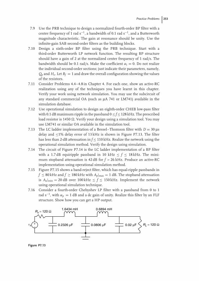
Practice Problems 253
7.9 Use the PRB technique to design a normalized fourth-order BP filter with acenter frequency of 1 rad s−1, a bandwidth of 0.1 rad s−1, and a Butterworthmagnitude characteristic. The gain at resonance should be unity. Use theinfinite-gain SAB second-order filters as the building blocks.
7.10 Design a sixth-order BP filter using the PRB technique. Start with athird-order Butterworth LP network function. The resulting BP structureshould have a gain of 2 at the normalized center frequency of 1 rad/s. Thebandwidth should be 0.1 rad/s. Make the coefficient a1 = 0. Do not realizethe individual second-order sections; just indicate their parameters, namely,Qp and Ho. Let Rf = 1 and draw the overall configuration showing the valuesof the resistors.
7.11 Consider Problems 4.4–4.8 in Chapter 4. For each one, show an active-RCrealization using any of the techniques you have learnt in this chapter.Verify your work using network simulation. You may use the subcircuit ofany standard commercial OA (such as µA 741 or LM741) available in thesimulation database.
7.12 Use operational simulation to design an eighth-order CHEB low-pass filterwith 0.1 dB maximum ripple in the passband 0 ≤ f ≤ 128 kHz. The prescribedload resistor is 1450 . Verify your design using a simulation tool. You mayuse LM741 or similar OA available in the simulation tool.
7.13 The LC ladder implementation of a Bessel–Thomson filter with D = 30 µsdelay and ≤1% delay error of 13 kHz is shown in Figure P7.13. The filterhas less than 2-dB attenuation in f ≤ 110 kHz. Realize the network using theoperational simulation method. Verify the design using simulation.
7.14 The circuit of Figure P7.14 is the LC ladder implementation of a BP filterwith a 1.7 dB equiripple passband in 10 kHz ≤ f ≤ 18 kHz. The mini-mum stopband attenuation is 42 dB for f > 26 kHz. Produce an active-RCimplementation using operational simulation method.
7.15 Figure P7.15 shows a band-reject filter, which has equal-ripple passbands inf ≤ 80 kHz and f ≥ 180 kHz with Ap|max = 1 dB. The stopband attenuationis Aa|min = 20 dB over 100 kHz ≤ f ≤ 150 kHz. Implement the networkusing operational simulation technique.
7.16 Consider a fourth-order Chebyshev LP filter with a passband from 0 to 1rad s−1, with αp = 1 dB and a dc gain of unity. Realize this filter by an FLFstructure. Show how you can get a HP output.
ns
Rs = 120 Ω
RL = 120 Ω
0.6894 mH1.6434 mH
0.2326 µF 0.0806 µF 0.02 µF+−
Figure P7.13

254 7 Higher-Order Active Filters
750
68.91
13.86 10.16
89.71
13.2410.63
205.9
2.04
5
1.56
8
(Ω, nF, mH)
Figure P7.14
1
1
1.099
1.601
2.237 2.237
0.78
65
0.78
65
(Ω, µF, µH)
Figure P7.15
7.17 Realize the transfer function
H(s) = V2
V1= a4s4 + a3s3 + a2s2 + a1s + a0
s4 + b3s3 + b2s2 + b1s + b0
by an FLF structure with feed-forward paths, but using lossy integrators ofthe form −1/(s + α).
7.18 Figure P7.18 shows an LC ladder network. Design the network using asuitable OTA-C structure. You may consider floating inductor simulationusing OTA.
7.19 Produce OTA-C-based implementations for Problems 7.2, 7.3, 7.6, 7.8−7.15.Verify the designs using a suitable network simulation tool. You may useLM 13 700 for a practical OTA.
7.20 Design a fourth-order switched-capacitor LP filter with a Butterworthmagnitude characteristic, a cutoff frequency of 1 kHz, and a clock frequencyof 100 kHz. Choose the minimum capacitance of 1 pF.
2.52.596
116.6
18.22 13.56
2.5
0.377
67.75 31.68
2.791
(kΩ, pF, µH)
Figure P7.18

255
8Current-Mode Filters
The advancements in IC technology together with the demand for smaller andlow-power devices have ushered in the era of IC filters. While the initial goalof microminiaturization was to produce filters for audio frequency applications,the focus has progressively changed toward higher-than- audio frequency filters.The advent of submicron IC technological processes (0.5 µm and smaller) hasfacilitated realization of filters in the VHF frequency band (30–300 MHz) (Rautand Guo, 1997). Together with higher frequency of operation, reduction in thepower consumption by the various electronic devices has also been of concernto present-day researchers. In view of this, attention is being paid toward signalprocessing in terms of currents rather than voltages. This new type of signalprocessing is known as current-mode signal processing.
It can be easily appreciated that CM signal processing will lead to higherfrequency of operation, since the signal current is delivered into a small (ideallyshort circuit) load resistance. The parasitic pole due to such a small resistance(pole frequency being inversely proportional to the resistance) will be very high andhence, a high-frequency signal can be processed without substantial impairmentdue to the presence of such a high-frequency parasitic pole. In this chapter, wefirst introduce the basic principles of CM signal processing. Realization techniquesfor second-order CM filters using several CCs (Sedra and Smith, 1970) will bepresented next. This will be followed by presenting techniques that can be usedto convert an existing voltage-mode (VM) filter to a CM filter using generalizedduals (GDs) and transposes; thus, the wealth of knowledge that already exists inthe classical area of VM filters can be readily and efficiently used. The discussionwill then continue with SI filters, the analog of SC filters for CM signal processing.
8.1Basic Operations in Current-Mode
8.1.1Multiplication of a Current Signal
The magnification or attenuation (i.e., multiplication by a constant) of a currentsignal is one of the fundamental operations required in CM filtering. Several
Modern Analog Filter Analysis and Design: A Practical Approach. Rabin Raut and M. N. S. SwamyCopyright 2010 WILEY-VCH Verlag GmbH & Co. KGaA, WeinheimISBN: 978-3-527-40766-8

256 8 Current-Mode Filters
alternatives exist to achieve this operation and a few of these are now brieflydiscussed.
8.1.1.1 Use of a Current MirrorA current mirror is the simplest device that can be used to multiply a current signalby a constant. The ideal mirror will function like a CCCS with zero input resistanceand an infinite output resistance. This is depicted in Figure 8.1. In a CMOS ICtechnology, the multiplication value is proportional to the ratio of the area of theMOS transistor at the output to the area of the MOS transistor at the input. Ifwe consider a simple CMOS current mirror as shown in Figure 8.2a, with its ACequivalent circuit as shown in Figure 8.2b, the current signal transfer ratio at lowfrequency will be given by
Io
Ii= gmn2 + gmp2
gmn1 + gmp1 + gdp1 + gdn1(8.1)
The condition of zero input resistance (inversely proportional to the sum gmn1 +gmn2 + gdp1 + gdp2) and infinite output resistance (inversely proportional to gdp2 +gdn2) are seldom achieved in practice. Special circuit configurations are used toachieve conditions close to these ideal ones.
I i → ← Ai I i
Figure 8.1 A current-controlled currentsource (CCCS).
V g mn
1V
g dn
1
g mn
2V
g dn
2g d
p2
g mp
2V
g dp
1
g mp
1V
I i → I i →← Io ← Io
MP1
MN1 MN2
MP2
+
−
(a) (b)
Figure 8.2 (a) Current mirror using CMOS transistors and(b) its AC equivalent circuit, where gdni, gdpi, i = 1, 2 areconductances.

8.1 Basic Operations in Current-Mode 257
8.1.1.2 Use of a Current ConveyorThe functional characteristic of a CC has been introduced in Chapter 5. CCII(Sedra and Smith, 1970) has become popular for practical applications since the1990s (Toumazou, Lidgey, and Haigh, 1990). The schematic for a CCII and thematrix showing its terminal i–v relationships are repeated here for convenience(Figure 8.3).
According to the relation iz = ±ix, the CCII is further categorized as positive (+)and negative (−) CCII, that is, CCII+ and CCII–. Figures 8.4a and 8.4b show theschematics of typical positive and negative gain CCs implemented in CMOS ICtechnology (Toumazou, Lidgey, and Haigh, 1990). Figure 8.4c shows how a CCII+and a CCII– can be used to multiply a current signal by a constant value.
±1
=iz
vx
iy vy
ixvz00
001
000
CCII zx
y
iy →
i x → ← i z
(a) (b)
Figure 8.3 (a) Symbol of a CCII and (b) i–v relations of the CCII.
VDD VDD
Y Z
X
VSS VSS
ix →Y
X
ix →← iz
+
−A
+
−A
(a) (b)
= ix
Z
← i z= − i x
I i →
Io →
(c)
R1
R2
X
Y Z
CCII(+/−)
Io = (±) I i
R2
R1
Figure 8.4 (a) Implementation of a CCII–, (b) implemen-tation of a CCII+, and (c) a current multiplier using CCII–.(a) and (b) taken from Toumazou, Lidgey, and Haigh 1990.

258 8 Current-Mode Filters
8.1.1.3 Use of Current Operational AmplifierA COA acts in the same way on the current signals as an OA acts on a voltage signal.It ideally approaches the characteristics of a CCCS. Thus, the input resistance needsto be small while the output resistance is required to be very high. Similarly, theshort circuit current gain is required to be high. A COA typically uses a cascade of atransimpedance amplifier (for low input resistance) followed by a transconductanceamplifier (for high output impedance). Figure 8.5 shows the schematic of a tunableCOA implemented in CMOS technology. The input is applied to the common-gateMOS amplifier stages of a transimpedance amplifier (Bruun, 1994) followed bya tunable transconductance stage (Assi, Sawan, and Raut, 1996). The circuit hasbeen implemented using differential-in differential-out (Bruun, 1991) topologyin a 0.8-µm BiCMOS IC technology. A summary of the simulated responsecharacteristics is presented in Table 8.1. More details can be found in Assi, Sawan,and Raut (1997).
I IN1 →
I IN2 →
IB1 IB3
IB2
IB1
IB2
VSSVDD
VDDVREF
IOUT2
IOUT1
IB3
VG1
M1 M2
M4
M3M2
VG1
M1
M4 M5
M5
M3
M6 M8
M10M11
M9 M7
Figure 8.5 A tunable COA implemented in CMOS technology.

8.1 Basic Operations in Current-Mode 259
Table 8.1 Simulated response of the tunable COA of Figure 8.5.
Gain (voltage controllable) 70–96 dBOutput current (peak-to-peak) 280 µAGBW 145 MHzSupply voltages VDD = −VSS = 1.5 VPower consumption <0.5 mW
8.1.2Current Addition (or Subtraction)
Current addition is obtained by simply connecting the paths on to a single node.For subtraction, the pertinent current signal has to be reversed before subjectingto addition. Crossing the wire is the conventional technique for reversing thecurrent. Figure 8.6 presents a typical circuit for achieving this operation in CMOSIC technology (Toumazou, Lidgey, and Haigh, 1990).
8.1.3Integration and Differentiation of a Current Signal
A simple current integrator is depicted in Figure 8.7a. The current Ii from an idealsource forms a voltage across the capacitor C. The OTA with a transconductancegm converts this voltage to a current at the output.
The transfer characteristic, in the ideal case, is given by
Io = gm
sCIi (8.2)
If the input current source has a finite resistance Ri = 1/ Gi, and the output is nota short circuit (for small signal), that is, RL = 0, then the response characteristic
VDD
VSS
VSS
VDD
ix → ← iz = −ix
Figure 8.6 Implementation ofthe reversal of a current signal.

260 8 Current-Mode Filters
gm
gmC
I i → I i →IoC
(a) (b)
↓Io
↓
+−
A simple current integrator
An alternative currentintegrator
Figure 8.7 Integration of a current signal.
I i →
Ii →
R
C
IoC
MN1 MN2 MN3
MP1 MP2 MP3
(a) (b)
↓
Io
↓
Figure 8.8 Current differentiator using (a) RC elements and (b) CMOS transistors.
will be that of a lossy integrator:
Io
Ii= gmRo
Ro + RL.
1
Gi + sC(8.3)
where Ro is the output resistance of the transconductor.A better alternative for the CM integrator is shown in Figure 8.7b. Since the
current source Ii feeds to the virtual ground terminal of the OA, the effect of the finitevalue of Gi will be insignificant. For finite Ro and RL, the transfer relation is given by
Io
Ii= gmRo
Ro + RL.
1sC
(8.4)
A CM integrator can also be obtained using a CCII+ or a CCII–; these are shownin Table 8.2.
A basic differentiator network for current signal is shown in Figure 8.8a. Theproduct RC should be ideally zero for perfect differentiation. An IC version inCMOS technology is shown in Figure 8.8b.
Considering finite transconductances of the MOS transistors, the transfercharacteristic equation is given by
Io
Ii= k
sC/Gm1
1 + sC(Gm1 + Gm2)/Gm1Gm2(8.5)
In the above, Gm1 is the equivalent input conductance of the (MP1, MN1) transistorpair, Gm2 that of the (MP2, MN2) transistor pair, and k is the current mirroring ratiobetween the pairs (MP3, MN3) and (MP2, MN2). We have ignored the parasiticcapacitances of the MOS transistors in deriving Eq. (8.5).

8.1 Basic Operations in Current-Mode 261
Tabl
e8.
2So
me
basi
cbu
ildin
gbl
ocks
usin
gC
CII
.
CC
IIci
rcui
tsTr
ansf
erfu
nctio
nR
emar
ks
AR
1
R2
I i→
I o→
X Y
CC
II(+
/−)
ZI o
=(±
)R2
R1
I iN
onin
vert
ing
and
inve
rtin
gcu
rren
tam
plifi
er
B
I 1→
I n→
I o→
I j→
I 2→
X Y
CC
II(+
/−)
ZI o
=(∓
)n ∑ j=
1I j
Inve
rtin
gan
dn
onin
vert
ing
curr
ents
um
mer
CR
C
I i→
I o→
X Y
CC
II(+
/–)
ZI o
=(±
)1
sCR
I iN
onin
vert
ing
and
inve
rtin
gcu
rren
tin
tegr
ator
DC R
I i→
I o→
X Y
CC
II(+
/−)
ZI o
=(±
)sC
RI i
Non
inve
rtin
gan
din
vert
ing
curr
entd
iffe
ren
tiat
or
(con
tinu
edov
erle
af)

262 8 Current-Mode Filters
Tabl
e8.
2(c
ontin
ued)
.
CC
IIci
rcui
tsTr
ansf
erfu
nctio
nR
emar
ks
E2 1
X YC
CII+
Z[ a
] =[ 1
00
0
]U
nit
y-ga
inV
CV
S
F1
X YC
CII−
Z2
[ a] =
[ 00
01
]U
nit
y-ga
inC
CC
S
GX Y
Z2
1g
CC
II(+
/−)
[ y] =
[0
0(∓
)g0
]V
CC
S
H
1X Y
CC
II(−/
+)Z
X YC
CII+
Z2
r[ z
] =[ 0
0(±
)r0
]C
CV
S

8.1 Basic Operations in Current-Mode 263
I
2 1
X YC
CII
+Z
[ a] =
[ 10
0−1
]U
nit
y-ga
inC
NIC
J
gg
1
2
X Y
CC
II(−
/+)
Z
X Y
CC
II(+
/−)
Z[ y
] =[
0(∓
)g(±
)g0
]Id
ealg
yrat
or
K
g2
g1
12
XX
YY
CC
II (−
/+)
CC
II (−
/+)
ZZ
[ y] =
[0
(±)g
1
(±)g
20
]N
egat
ive
impe
dan
cein
vert
er(N
II)

264 8 Current-Mode Filters
8.2Current Conveyors in Current-Mode Signal Processing
8.2.1Some Basic Building Blocks Using CCII
In Section 8.1.1, it has been shown how CCII+ and CCII– can be used as currentsignal multiplying devices. Some examples of signal processing operations usingCCII are presented in Table 8.2.
8.2.2Realization of Second-Order Current-Mode Filters
In the following sub-sections, we discuss several cases of implementation ofsecond-order CM filters using CCs.
8.2.2.1 Universal Filter ImplementationSince a CC can transport current signals, it can be used together with passive-RCcomponents to realize CM transfer functions in the same way as an OA is usedto produce VM transfer functions. Figure 8.9 presents a universal CM filter witha single input and three outputs. The configuration uses both CCII+ and CCII–
Z CCII−Y
X
R3
Z CCII+
CCII−
CCII+
Y
X
R2
R4
C2C1
R6 R7
R5
R8
R1
Y
XZ
I i
Y
X
Y
Y
X
X
Z CCII+
CCII−
Z
Z
Y
XCCII+ Z
Ihp IbpIlp
Figure 8.9 A universal second-order CM filter implemented with CCII+ and CCII–.

8.2 Current Conveyors in Current-Mode Signal Processing 265
as the active building blocks. The three primary transfer functions are given by(Chang, 1993), with Gi = 1/Ri(i = 1, 2, 3, . . .):
Ihp
Ii= s2C1C2G6
s2C1C2G1 + sC1G2G4 + G3G4G5(8.6)
Ibp
Ii= −sC1G4G7
s2C1C2G1 + sC1G2G4 + G3G4G5(8.7)
Ilp
Ii= G4G5G8
s2C1C2G1 + sC1G2G4 + G3G4G5(8.8)
By connecting the Ihp and Ilp outputs, we get the notch filter response. Similarly,by adding the three outputs and assuming G6 = G1, G7 = G2, and G8 = G3, we getan AP characteristic (Senani, 1992). The pertinent transfer functions are
Inotch
Ii= s2C1C2G6 + G4G5G8
s2C1C2G1 + sC1G2G4 + G3G4G5(8.9)
Iap
Ii= s2C1C2G1 − sC1G2G4 + G3G4G5
s2C1C2G1 + sC1G2G4 + G3G4G5(8.10)
The pole frequency ωp and Qp the pole Q are given by
ωp = (G3G4G5/C1C2G1)1/2
Q p = (1/G2)(G1G3G5C2/C1C4)1/2 (8.11)
It may be noted that the ωp and Qp are tunable by adjusting R3 and R2, in that order.The CCs can be implemented using commercial OAs such as, LF356N, followedby current mirrors composed of transistor arrays (CA3096AE).
8.2.2.2 All-Pass/Notch and Band-Pass Filters Using a Single CCIIFigure 8.10 shows a CM AP/notch and BP filter using a single negative gain CCII.The network needs two grounded capacitors, and (at most) four resistors. The CTF
I i →Io →
R1
R6
C4
C5R2
R5
X
Y
CCII− Z
Figure 8.10 All-pass, band-pass, and notch filters using a single CCII–.

266 8 Current-Mode Filters
is given by (Chang, 1991)
Io
Ii= s2G1C4C5 + s(G1C4C5 + G1G2C5 − G2G6C4) + G1G2G5
(G1 + G2)[s2C4C5 + s(G5C4 + G2C5) + G2G5](8.12)
The BP case arises on selecting G1 = 0 (i.e., R1 open circuit). The notch filterrealization is possible with G6 = (C4G5G1 + C5G2G1)/G2C4, and the AP filter isrealized by the choice G6 = 2(C4G5G1 + C5G2G1)/G2C4. The pole frequency ωp
and the pole Q are given by
ωp =√
G2G5
C4C5,
1
Q p=√
C4G5
C5G2+√
C5G2
C4G5(8.13)
8.2.2.3 Universal Biquadratic Filter Using Dual-Output CCIIA dual-output current conveyor type 2 (DOCCII) is a more versatile building blockthan a single-output CCII and an implementation using CMOS technology hasalready been given in Figure 5.33. The operation of a DOCCII is described by thematrix equation
Vx
Iy
Iz1
Iz2
=
0 1 0 00 0 0 01 0 0 0k 0 0 0
Ix
Vy
Vz1
Vz2
(8.14)
If k = 1, then DOCCII+ is defined and if k = −1, then DOCCII– is defined.Four DOCCII+ configured as in Figure 8.11 can function as a universal CM
biquadratic filter (Minaei, Kuntman, and Cicekoglu, 2000). Analysis of the circuitleads to
Io1
Iin= −y2y4/,
Io2
Iin= −y4y5/,
Io3
Iin= −y3y5/ (8.15a)
where
= y4y6 + y3y5 − y1y4 (8.15b)
Suitable selection of the admittance elements y1, y2, . . . , y6 will lead to realization ofseveral second-order filters. Choosing y1 = 0, y2 = G2, y3 = sC3, y4 = G4, y5 = sC5,and y6 = G6 + sC6 will lead to
Io1
Iin= −(G2G4/C3C5)/,
Io2
Iin= −s(G4C5/C3C5)/,
Io3
Iin= −s2/
(8.16a)
where
= s2 + (G4C6/C3C5)s + (G4G6/C3C5) (8.16b)
The above equations represent, respectively, an LP, a BP, and an HP filter. Byadding the outputs Io1 and Io3 and making G2 = G6, one can get a regular notch

8.3 Current-Mode Filters Derived from Voltage-Mode Structures 267
y1
y3
y4
y2
y6
y5I in
Io3 Io2
Io1
Y Y Y
Y
X X X
X
DOCCII+#1
DOCCII+#2
DOCCII+#3
DOCCII+#4
Z1 Z1 Z1
Z2Z2 Z2
Z1
Z2
Figure 8.11 A universal second-order CM filter using dual-output current conveyors.
filter. The pole frequency and pole Q are given by
ωp =√
G4G6
C3C5, Q p = 1
C6
√C3C5G6
G4(8.17)
It is seen that ωp and Q p can be tuned orthogonally by adjusting grounded passiveelements. It is also readily seen that the sensitivity of Q p w.r.t. G2 as well as that ofωp w.r.t. C6 and G2 are zero, that of Q p w.r.t. C6 is −1, while the magnitudes of thesensitivities of ωp and Q p w.r.t. the remaining passive elements are 0.5. Thus, thesensitivities w.r.t. the passive elements are not greater than unity.
8.3Current-Mode Filters Derived from Voltage-Mode Structures
As mentioned earlier, the IC technology has made CM signal processing an areaof immense interest. However, it should be pointed out that the concept of CMfilters itself is not new and goes back to the 1950s when Thomas (1959) proposedstructures for realizing CTFs using voltage- and current-inverting NICs.
The concept of deriving a CM structure from a VM one goes back historically to1971, when Bhattacharyya and Swamy (1971) introduced the concept of networktransposition, whereby given a network N with an admittance matrix [y], one couldeasily convert it to another network NT whose admittance matrix is the transpose

268 8 Current-Mode Filters
of [y]. They also derived the transposes of standard two-port elements such as thecontrolled sources, impedance converters, and impedance inverters. Their basicintention was to obtain a structure realizing a CTF, which is identical to the VTFof a given VM structure, as well as to obtain alternate structures for DPIs. Theyalso pointed out that the transpose was essentially the same as the adjoint networkof Director and Rohrer (1969), who had defined the latter two years earlier inconnection with the calculation of sensitivities. Swamy, Bhusan, Bhattacharyya(1974, 1976) also defined generalized duals (GDs) and generalized dual transposes(GDTs), and gave a graphical method of obtaining the GD for a two-port networkconsisting of one-ports and three-terminal two-ports as subnetworks. Some of thismaterial has been treated in Chapters 2 and 3. It is only after the advent of ICtechnology, have these ideas become useful. In the late 1980s and early 1990s,Roberts and Sedra, unaware of these ideas, resuggested the use of adjoints inobtaining a network whose CTF is the same as the VTF of a network realized usingOAs (Roberts and Sedra, 1989, 1992). Later, Carlosena and Moschytz presentedthe concept of nullor representation of the active devices to arrive at a CTF from agiven VTF (Carlosena and Moschytz, 1993). They specifically addressed the case ofVM to CM conversion by considering VCVS (or OA)-based VM filters (Moschytzand Carlosena, 1994).
It was shown in Chapter 3 that if the chain matrix of a given network N is
[a]N =[
A BC D
](8.18)
then the chain matrix of the reversed transposed network NTR , obtained by trans-
posing N and reversing the input and output ports of the transposed network, isgiven by
[a]NT
R=[
D BC A
](8.19)
Also, the chain matrix of the GD network ND has been defined in Chapter 3 as
[a]ND=[
D Cf (s)B
f (s) A
](8.20)
where f(s) is an arbitrary function of s. It is seen from Eqs. (8.18), (8.19), and (8.20),and as already pointed out in Chapter 3, that the CTF of NT
R as well as that of ND
is the same as the VTF of N. Thus, we can derive two structures for the CTF fromthat of a VTF through the GD and transposition operations.
In the next two sections, we will deal with the transformation of a VM filter N toa CM filter using the GD and transposition operations.

8.4 Transformation of a VM Circuit to a CM Circuit Using the Generalized Dual 269
8.4Transformation of a VM Circuit to a CM Circuit Using the Generalized Dual
To illustrate the procedure, let us consider the simple circuit of Figure 8.12a, whichrealizes the first-order VTF given by
Vout
Vin= K(G1 + sC1)[
G1 + (1 − K)G2] + s
[C1 + (1 − K)C2
] (8.21)
Vin Vout
R1 N1 N2
R2
C1
C2
K1
3
2
4
13
2
4
(N1)D (N2)D13
2
4
R2
C2
3 2
4
KinI outI
1 2
4
R1 R2
C1 C2
I in IoutK
Iout = KI in
Dual of OAof gain K
(a) (b)
(c) (d)
(e) (f)
Figure 8.12 (a) A first-order VM circuit us-ing a voltage amplifier (VA) of gain K; (b)the circuit in (a) being considered as a cas-cade of two three-terminal two-ports; (c)dual of the network in (b); (d) (N2)D, the
capacitive dual of the network N2; (e) cur-rent amplifier (CA) of gain K, the capacitivedual of a VA of gain K; and (f) the dual ofthe VM circuit shown in (a).

270 8 Current-Mode Filters
The circuit of Figure 8.12a can be thought of as a cascade of two networks N1 andN2, as shown in Figure 8.12b. We know from Theorem 3.1 that the GD of a cascadeof two-ports is the cascade of the GDs of the individual two-ports; hence, we mayfind the GD of the circuit of Figure 8.12b to be as shown in Figure 8.12c. FromTheorem 3.2, we have the result that the GD of a series element of impedance z(s)is a shunt element of impedance f(s)/z(s). If we now choose f (s) = 1/ s, (i.e., if wetake the capacitance duals), we see that (N1)D is nothing but a shunt element ofimpedance z1D = (1/ s)(G1 + sC1) = (1/sR1) + C1; thus, z1D is the impedance of ashunt element consisting of a series combination of resistor of C1 and a capacitorof R1 farads. Further, from the result of Problem 3.2, we see that (N2)D is thecapacitive dual of the VA of gain K in series with the dual of R2 and C2 in parallel.This is shown in Figure 8.12d. Now, the chain matrix of a VA of gain K is given by[ 1
K 00 0
]
Hence, using Eq. (8.20), the capacitive dual of the VA has the chain matrix[0 00 1
K
]
which is nothing but a CA of gain K, which is symbolized as shown in Figure 8.12e.Thus, the dual of the given network is as shown in Figure 8.12f.
From this very simple example, we can observe the following:
1) The dual of an RC-VA circuit can be obtained as an RC-CA circuit by employingthe capacitive dual.
2) The active element, namely, the VA, which was grounded in the originalnetwork, has become a floating active element in the dual network. Thisis due to the fact that the dual of the feedback arm in the original cir-cuit appears in series with the active element in the dual network. This isalways the case in that whenever we have a feedback path for the activeelement in the original network, the grounded active element is convertedto a floating dual active element in the dual network. This makes the ap-proach of obtaining CM circuits from VM circuits using GDs not a veryattractive one for implementation in IC technology, in view of the atten-dant influence of parasitic capacitances and enhancement of common-modenoise.
3) If the active element in the original circuit is an OTA of transconductance gm
or a operational transresistance amplifier (OTRA) of transresistance r, thentheir respective GD elements would be an OTRA of transresistance f(s)gm
and an OTA of transconductance r/f(s), respectively. If f(s) is chosen as 1/sto make sure that the passive-RC network part is converted into another RCnetwork, then the transadmittances of the OTAs and the transimpedancesof the OTRAs in the dual network are no longer resistive in nature, andbecome capacitive. On the other hand, if f(s) is chosen as unity so as to makethe transadmittances of the OTAs and the transimpedances of the OTRAsin the dual network to be resistive in nature, then the passive resistor and

8.5 Transformation of VM Circuits to CM Circuits Using Transposition 271
capacitor elements would be transformed into resistors and inductors in thedual network. Thus, the GD is not beneficial for use in obtaining CM filtersfrom VM filters if we have active elements such as OTAs, OTRAs, or impedanceinverters.
Hence, the GD does not play an important role in converting VM circuits toCM circuits. We will next consider the application of transposition in deriving CMcircuits from VM circuits.
8.5Transformation of VM Circuits to CM Circuits Using Transposition
We saw in Chapter 3 that the transpose of any given network N can be verysimply obtained by replacing the nonreciprocal subnetwork of N by its respectivetranspose. It was also seen that the transpose of a VCVS is nothing but a CCCSwith its input and output ports reversed and whose current gain is the same asthe voltage gain of the VCVS. Hence, for any circuit N that has been designedusing finite gain VAs, we may obtain its transpose NT by simply replacing eachof the VAs in N by a CA of the same gain, but with its input and output portsinterchanged. Then, the reverse CTF of the transposed network is identical to theforward VTF of the original network and vice versa. It should also be noted that thecorresponding sensitivities of the CTF and VTF w.r.t. the various elements wouldbe the same.
The importance of the transpose is particularly apparent in the case of circuitsthat employ OTAs. Since the transpose of a VCCS is itself with its input–outputports reversed, when a network N containing OTAs is transposed, the resultingnetwork will also consist of only OTAs (i.e., no new active element is necessary).It is obvious that similar results hold good for any VM network designed usingOTRAs.
The single-input single-output relationship between the VTF of a VM circuitand the reverse CTF of its transpose can be extended easily to multiport networks.Consider a network N consisting of (n + m + 1) terminals with n input ports and moutput ports realizing a VTF matrix [Tv ]. We can easily find its transpose NT usingthe procedure outlined above. Then the roles of the input and output ports arereversed in the resulting network (i.e., the m output ports and the n input ports inN now become the m input and n output ports respectively). Then the CTF matrix[Ti] of this m-input n-output port network is the same as [Tv ]T . Interested readerscan refer to Bhattacharyya and Swamy (1971) for the proof. We will later take anexample to illustrate the usefulness of this result.
Finally, it should be emphasized that the transpose (or adjoint) operation isuseful for not only deriving structures for CTFs, but also for obtaining alternatestructures for driving point functions as well as for transfer impedance and transferadmittance functions.

272 8 Current-Mode Filters
8.5.1CM Circuits from VM Circuits Employing Single-Ended OAs
As mentioned earlier, the transpose of a VCVS of gain A is a CCCS of gain Awith its input and output ports interchanged. For an infinite-gain OA (A → ∞), itstranspose is a COA of infinite gain. This is symbolically shown in Figure 8.13.
We now illustrate the method of obtaining CM circuits from OA-based VMcircuits. We first take the case of a filter that employs a finite gain VA (which canbe realized using an OA), and then two filters that employ infinite-gain OAs.
8.5.1.1 CM Biquads Derived from VM Biquads Employing Finite Gain AmplifiersConsider the LP Sallen and Key VM structure of Figure 5.4, shown as Figure 8.14afor convenience. We know from Eq. (5.13) that its VTF is given by
Vo
Vi=
K(G1G3)
C2C4
s2 + s
(G1
C2
)+(
G3
C2
)+ (1 − K)
(G3
C4
)+ G1G3
C2C4
(8.22)
One can easily obtain the transpose by replacing the OA of gain K by a COA ofgain K with its ports reversed and leaving the other elements intact. The resultingCM circuit is shown in Figure 8.14b. It can easily be verified that the reverse shortcircuit CTF of Figure 8.14b is the same as the forward VTF given by Eq. (8.22).
Similarly, it can be shown that the type 1 and type 2 sensitivity-compensatedactive networks proposed by Daggett and Vlach (1969) for CTF and VTF are, infact, transposes of each other.
Vi
VoA A
I i = 0
Ii
Vi = 0
Io
−
+ (A → ∞)
(A → ∞)(a) (b)
Figure 8.13 (a) An infinite-gain OA and (b) its transpose, a COA of infinite gain.
Vi IiVoR1 R1 R3R2
C4
C2 C2
C4
K K
Io
(a) (b)
Figure 8.14 (a) Sallen and Key LP VM filter and (b) itscorresponding CM filter obtained using transposition.

8.5 Transformation of VM Circuits to CM Circuits Using Transposition 273
8.5.1.2 CM Biquads Derived from VM Biquads Employing Infinite-Gain AmplifiersConsider the general VM single-OA biquad of Figure 5.6, which is redrawn asshown in Figure 8.15a for the sake of convenience. It can be shown that the VTFof Figure 8.15a is given by
Tν (s) = Vo
Vi= −Y1Y3
[Y5 (Y1 + Y2 + Y3 + Y4) + Y2Y3] + 1A
× [(Y1 + Y2 + Y4) (Y3 + Y5) + Y3Y5](8.23)
As A → ∞, the above reduces to
Tν (s) = Vo
Vi= −Y1Y3
[Y5 (Y1 + Y2 + Y3 + Y4) + Y2Y3](8.24)
We can easily get the transpose of the VM circuit by replacing the OA in the circuitby a reversed COA of infinite gain as shown in Figure 8.15b.
We can verify that for the transposed network, the reverse CTF, Ti(s), is the sameas the VM VTF, Tv(s) given by Eq. (8.24). It should be pointed out that A → ∞only in theory. In practical situations, A is large but finite, and is a function of thecomplex frequency s. Hence, in order to study the behavior of Tv(s) or Ti(s) underpractical conditions, one has to substitute the appropriate expressions for the gainA(s) for the OA or the COA, as the case may be.
The same procedure can be used to transpose any VM circuit that employs mul-tiple OAs with infinite gain. For example, if one considers the VM Fleischer–Tow
A
A → ∞
A → ∞
Vi
Io
Vo
Y1
Y1
Y2
Y3
Y5
Y4
Y2
Y4
Y3
Y5
AIi
−
+
(a)
(b)
Figure 8.15 (a) A single-amplifier VM general biquad and (b) its transpose.

274 8 Current-Mode Filters
C1
R3
R1
R4 R6
R7
R8
R2
C2
R5
Io
Ii
∞ ∞ ∞
Figure 8.16 Transpose of the Fleischer–Tow VM biquad.
biquad of Figure 5.10, one can easily obtain the corresponding CM structure by sim-ply replacing the OAs by reversed COAs of infinite gain, as shown in Figure 8.16.It can be verified that the CTF of the CM circuit is the same as the VTF of theoriginal, as given by Eq. (5.47).
8.5.2CM Circuits from VM Circuits Employing OTAs
8.5.2.1 VM Circuits Using Single-Ended OTAsIf one of the input terminals of the OTA (see Figure 5.17) is grounded, saythe negative terminal, then the OTA and its equivalent circuit are as shown inFigure 8.17. Its admittance matrix is
[y]N =[
0 0−gm 0
]
Hence, the admittance matrix of its transpose is
[y]TN =[
0 −gm
0 0
]
VaVa VC
Va Vc
VcgmgmgmVa gmVa
gmVa
++
+
−
Ia = 0Ic
(a) (b) (c)
Figure 8.17 (a) and (b) Symbols for an OTA whosepositive terminal is grounded, and (c) its AC equivalent cir-cuit.

8.5 Transformation of VM Circuits to CM Circuits Using Transposition 275
Va
Vb
Va
Vb
Vc
Vc
T
gm
gmVa
gmVb
gmVc
gmVc
Vc
VcT
+
gm−
gm
−
gm+
(a)
(b)
Figure 8.18 (a) OTA with its negative input terminalgrounded and its transpose (b) OTA with its positive inputterminal grounded and its transpose.
which corresponds to nothing but the original OTA with its input and output portsinterchanged. Similarly, if the positive input terminal of the OTA is grounded,then the corresponding transpose would be itself with its input and output portsinterchanged. These are symbolically shown in Figure 8.18. Thus, the transpose ofa single-ended OTA is itself and is not a new element. This is particularly usefulsince the same element can be used for both the VM and CM circuits.
As an example (Swamy and Raut, 2002), consider the VM gm-C BP filteremploying single-ended OTAs (Ghausi and Laker, 1981), as shown in Figure 8.19a.The corresponding CM filter can readily be obtained using transposition and isshown in Figure 8.19b. It is easily verified that the VTF of the former and thereverse CTF of the latter are indeed the same and are given by (Senani, 1992)
Vo
Vi= Io
Ii= sC1gm2
s2C1C2 + sC1gm3 + gm1gm2(8.25)
Vi VoIo
C1 C2
C2C1
gm1
Ii
(a) (b)
+
gm2 gm3
gm2
gm1
+ −
+
+
gm3−
Figure 8.19 (a) VM gm-C BP filter employing single-endedOTAs and (b) the corresponding CM filter (transpose of thecircuit in (a)).

276 8 Current-Mode Filters
Obviously the sensitivities of the pole frequency and pole Q of both the VTF andCTF are the same w.r.t. the various parameters.
We now consider an example of obtaining a CTF matrix from a network realizinga VTF matrix (Swamy and Raut, 2002). Figure 8.20 shows a general VM biquadstructure that realizes LP, BP, and HP functions depending on whether the input isVA, VB, or VC (Geiger and Sanchez-Sinencio, 1985). This structure can be consideredas a three-input single-output network realizing the VTF matrix [Tv] given by
Vo = [Tν ]
VA
VB
VC
= 1
D(s)
[gm2gm5 sC1gm4 s2C1C2
] VA
VB
VC
(8.26a)
C2
Vo
Vc
C1
VBVA
gm1
gm5
IBIA
Ii
−
+
gm1 C1 C2
Ic
−gm2
gm3+ −
gm4
+gm5
+
gm2
gm4
gm3+
+
−
(a)
(b)
Figure 8.20 (a) A three-input single-output VM biquadstructure realizing LP, BP, and HP functions and (b) itstranspose, a single-input three-output CM biquad structure.

8.5 Transformation of VM Circuits to CM Circuits Using Transposition 277
where
D(s) = s2C1C2 + sC1gm3 + gm1gm2 (8.26b)
The transpose of the given network is as shown in Figure 8.20b. This is asingle-input three-output network realizing the CTF matrix [Ti] = [Tv ]T . Thus, theCM filter realizes the CTF matrix
IA
IB
IC
= 1
s2C1C2 + sC1gm3 + gm1gm2
gm2gm5
sC1gm4
s2C1C2
Ii (8.27)
This realization is the same as the one given by Senani (1992).
8.5.2.2 VM Circuits Using Differential-Input OTAsIn the above section, we derived CM circuits from VM circuits that employsingle-ended OTAs. We now consider the transformation of VM circuits employingdifferential-input single-output (DISO) OTAs to CM circuits. For this, we first derivethe transpose of a DISO-OTA, as shown in Figure 8.21a.
The [y] of the differential-input OTA is given by IA
IB
IC
=
0 0 0
0 0 0−gm gm 0
VA
VB
VC
(8.28)
Hence,
[y]T = 0 0 −gm
0 0 gm
0 0 0
(8.29)
Thus, in the transposed element, the current–voltage relations are
IA = −gmVC, IB = gmVC, IC = 0 (8.30)
Thus the transpose of a DISO-OTA is a single-input dual-output (SIDO) OTA; itis symbolically shown as in Figure 8.21b. A SIDO-OTA can be obtained by simply
VAIA
IB
ICVB
gm VC
gmVC
gmVC
VCVB
VC
VA
gmVC
VCgm
+
− gm
++
gm−
gm
+
−
(a) (b) (c)
Figure 8.21 (a) A DISO-OTA, (b) its transpose, aSIDO-OTA, and (c) a realization of a SIDO-OTA.

278 8 Current-Mode Filters
applying a current replica in a standard OTA. A simple realization using twosingle-ended OTAs is shown in Figure 8.21c. Using the transpose of a DISO-OTA,we can easily derive CM circuits from VM circuits that employ such OTAs. Weillustrate this with two examples.
Example 8.1. SIDO-OTA universal CM filter: Consider the VM DISO-OTA univer-sal filter shown in Figure 8.22a (Deliyanis, Sun, and Fidler, 1999). It can be shownthat the VTF of this circuit is given by
Tν (s) = Vo
Vi= gmY2Y4
D(s)(8.31a)
where
D(s) = (Y1Y2 + Y2Y3 + Y3Y1) (Y4 + Y5) + (Y1Y5 + Y2Y5 + gmY2
)Y4
(8.31b)
By replacing the DISO-OTA by its transpose, we get the CM filter shown inFigure 8.22b, proposed by Al-Hashimi and Fidler (1988). It can easily be shownthat the CTF Ti (s) = Io
Iiis given by
Ti (s) = Io
Ii= gmY2Y4
D (s)
which is the same as the Tν (s) of the original network. Various filters such as LP,BP, and HP second-order filters can be obtained by appropriately choosing thevalues of the various admittances.
Example 8.2. Leapfrog structure: As a second example, we consider the derivationof the CM leapfrog structure from that of a VM leapfrog structure. Consider theladder network of Figure 7.38. The realization of this ladder for its VTF usingDISO-OTAs is shown in Figure 7.40 and is redrawn as Figure 8.23 for convenience.The various impedances Z′
1, Z′2, . . . , Z′
6 in Figure 8.23 are related to the seriesand shunt passive impedances Z1, Z2, . . . , Z6 of the ladder of Figure 7.40 by therelations
Z′j = 1
ggmj
1
Zj, for j = 1, 3, 5 (8.32a)
Vi Y5 Y3 Y1 Y5 Y3 Y1
IiY2Y4Y4 Y2
VoIo
gm
−
+ gm
−+
+
(a) (b)
Figure 8.22 (a) A universal VM filter using a DISO-OTA,(b) its transpose, the CM counterpart of the circuit givenin (a).

8.6 Derivation of CTF Structures Employing Infinite-Gain Single-Ended OAs 279
z1′ z2′ z3′ z4′ z5′ z6′
gm1 gm2 gm3 gm4 gm5 gm6
ViVo
−+
−+
−+
−+
−+ +
Figure 8.23 VM leapfrog structure for the ladder network of Figure 7.48 using OTAs.
z1′ z2′ z3′ z4′ z5′ z6′
gm1 gm2 gm3 gm4 gm5 gm6
IiIo
−+
+ −+ +
−+
+−+
+−+
+ +
Figure 8.24 Transpose of Figure 8.23, the corresponding CM leapfrog structure.
and
Z′j = 1
gmjZj, for j = 2, 4, 6 (8.32b)
Since these elements are unchanged in the transpose and only the DISO-OTAsare replaced by their transposed elements, which are SIDO-OTAs, the CM leapfrogstructure can readily be drawn, as shown in Figure 8.24. The CTF Io
Iiof the CM
structure is the same as the VTF of the VM structure of Figure 8.23.
Thus, any VM structure that is realized using OTAs can easily be transformed toderive corresponding CM structures that also use OTAs. In this connection, it is tobe noted that the various canonical structures derived for CM structures (Sun andFidler, 1995) and for VM structures (Sun and Fidler, 1997) are simply transposes ofone another (Tang, 2004). Even though the subject matter of this book is on filterdesign, we would like to point out that transposition can also be used to obtainalternate structures for oscillators from known oscillator structures (Bhattacharyya,Sundaramurthy, and Swamy, 1981; Swamy, Raut, and Tang, 2004; Tang, 2004).We next consider the application of transposition in conjunction with the conceptof nullors to obtain structures for CTFs that employ single-ended OAs from VMcircuits realized using single-ended OAs.
8.6Derivation of CTF Structures Employing Infinite-Gain Single-Ended OAs
In Section 8.5.1, we gave a method of transforming VM circuits using single-endedOAs into CM circuits; however, the CM circuits need to use COAs of infinite

280 8 Current-Mode Filters
gain. We will now show, using the principle of nullors along with the concept oftransposes, how to derive structures for CTFs that utilize infinite-gain OAs fromVTF structures that also employ infinite-gain OAs (Raut, Swamy, and Tian, 2007).
Consider a structure N that uses ideal single-ended OAs for the realization of agiven VTF. Since an ideal OA can be considered as an ideal VCVS of infinite gain,we may replace the VCVSs by their nullor equivalents. We now use the fact thatthe nullor equivalent of an ideal CCCS is exactly the same as that of the ideal VCVS(Bruton, 1980). Hence, we can replace each of the OAs in the VTF structure by anideal CCCS, and the VTF realized by the resulting structure N′ is the same as thatof N. If we now transpose the VTF structure N′ to obtain [N′]T, then each of theCCCSs in N′ would be replaced by a VCVS (infinite-gain OA) with its input andoutput ports reversed. Utilizing the property of a transposed network, we see thatthe reverse CTF of [N′]T is the same as the VTF of N. Since all the passive elementsin N are unchanged during these operations, it is clear that the CTF structureis obtained simply by reversing the input–output ports of the OAs. We will nowillustrate the usefulness of this result by the following examples.
8.6.1Illustrative Examples
8.6.1.1 Single-Amplifier Second-Order Filter NetworkConsider the SAB VM filter using an ideal OA (an ideal VCVS), as shown inFigure 8.25. The VTF of this network is given by
Vo
Vi= − Y3Y4
Y1Y2 + Y2Y3 + Y1Y3 + Y1Y4(8.33)
If we now replace the ideal VCVS by its nullor equivalent, and use the fact thatthe nullor equivalents of all the four ideal controlled sources are the same, we canreplace the ideal VCVS in Figure 8.25a by an ideal CCCS to obtain the VM circuitusing a CCCS, as shown in Figure 8.25b (where A tends to infinity), whose VTFshould be the same as that of the circuit of Figure 8.25a. In fact, it can easily beverified that this is true.
If we now take the transpose of the circuit of Figure 8.25b, we get the circuitshown in Figure 8.26, whose reverse CTF would be the same as the VTF of that of
Vi
Vi
Vo
Vo
Y4 Y3
Y1
Y2
Y4 Y3
Y2
Y1
Va
A = ∞ A → ∞−
+
(a) (b)
IAI
Figure 8.25 (a) A single-amplifier VM filter using an idealOA and (b) its nullor equivalent using a CCCS.

8.6 Derivation of CTF Structures Employing Infinite-Gain Single-Ended OAs 281
Io
IiY4 Y3
Y1
Y2
A = ∞−
+
Figure 8.26 Circuit obtainedfrom Figure 8.25a with its CTFsame as that of the VTF of thelatter.
Figure 8.25b, that is, the same as that of Figure 8.25a. It can indeed be verified thatthe reverse CTF Io/Ii of the CM filter of Figure 8.26 is given by
Io
Ii= − Y3Y4
Y1Y2 + Y2Y3 + Y1Y3 + Y1Y4(8.34)
As mentioned earlier, the circuit of Figure 8.26 could have been obtained directlyfrom the VTF circuit of Figure 8.25a by simply turning around the input and outputports of the VCVS.
8.6.1.2 Tow-Thomas BiquadThe Tow–Thomas VM filter NV , employing three OAs is shown in Figure 8.27. ItsVTF is given by
Vo
Vi= −
C1
Cs2 + 1
RC
(R
R1− r
R3
)s + 1
C2RR2
s2 + 1CR4
s + 1C2R2
(8.35)
The corresponding CTF network NC can be obtained directly by reversing theinput/output ports of each of the VCVS elements in Figure 8.27, and is shown inFigure 8.28. It can be verified that the reverse CTF of this circuit is given by
Io
Ii= −
[C1
Cs2 + 1
CR
(R
R1− r
R3
)s + 1
C2RR2
]
s2 + 1
CR4s + 1
C2R2
(8.36)
which is the same as the VTF of the VM filter of Figure 8.27
Vi
VoR1
R4
C1
C
−
+A = ∞ −
+A = ∞ −
+A = ∞
R
C
R2R3
r
r
Figure 8.27 Tow–Thomas VM filter N employing three OAs.

282 8 Current-Mode Filters
R4
C
R9C1
C
R2 R3
I2
I1I3I i Io
Vc
X3R
X2
r
R
VB
VAr X1
A = ∞−
+
A = ∞−
+
A = ∞−
+
Figure 8.28 Filter whose CTF is the same as the VTF of Figure 8.27.
8.6.1.3 Ackerberg and Mossberg LP and BP FiltersAs a final example, consider the Ackerberg and Mossberg filter, which can produceboth LP and BP filter responses depending upon the choice of the output signalnode, as shown in Figure 8.29 (Ackerberg and Mossberg, 1974). The two VTFs ofthe A & M filter are
Vo1
Vi= − s/RC1
s2 + s1
R1C1+ r1
C1C2R2rr2
(8.37a)
and
Vo2
Vi= −
r1
C1C2Rrr2
s2 + s1
R1C1+ r1
C1C2R2rr2
(8.37b)
Figure 8.30 shows the corresponding CTF network NC obtained directly from theVM filter by reversing the input/output ports of each of the VCVS elements in
Vi R
R1
C1
+
−A = ∞
−
+A = ∞
−
+A = ∞
r2
r
Vo1 Vo2
R2
C2
r1
Figure 8.29 Ackerberg and Mossberg filter realizing LP and BP functions.

8.6 Derivation of CTF Structures Employing Infinite-Gain Single-Ended OAs 283
R1
R
C1C2
r
R2
r1
r2
Vc+
−
+− Ii 2
Va+
−
Ii1Io
Vb
A = ∞
A = ∞
A = ∞
Figure 8.30 Filter whose CTFs are the same as the LP and BP VTFs of Figure 8.29.
Figure 8.29. It can easily be shown that the two CTFs are given by
Io
Ii2= −
r1
C1C2Rrr2
s2 + 1
R1C1s + r1
C1C2rr2R2
with Ii1 = 0 (8.38a)
and
Io
Ii1= −
1
RC1s
s2 + 1
R1C1s + r1
C1C2rr2R2
with Ii2 = 0 (8.38b)
which are, respectively, the same as the VTFs (Vo2/V1) and (Vo1/V1) of the VMfilter of Figure 8.29.
Thus, we can obtain a CTF (VTF) filter from a VTF (CTF) filter that employsthree-terminal ideal VCVSs by simply reversing the input/output terminals ofeach of the VCVSs in the latter. Similarly, we can conclude that if the VTF (CTF)filter consisted of only three-terminal CCCS elements, then we can obtain thecorresponding CTF (VTF) filter by simply reversing the input/output terminals ofthe CCCSs in the former.
8.6.2Effect of Finite Gain and Bandwidth of the OA on the Pole Frequency, and Pole Q
The analysis in the previous section has been made under the assumption ofideal passive components and ideal active devices (i.e., ideal OAs). However, it isimportant to study the effect of the nonideal characteristics of the active device.Since the active device used is the OA, one important deviation from its idealcharacteristic arises because of the limited amplifier bandwidth. We now analyzethe effect of finite bandwidth on the pole frequency and pole Q factor of the CTFfilter and compare them with those of the corresponding VTF filter.
The analytical procedure is demonstrated for a multi-OA filter, namely, theA & M three-OA biquad. For the A & M filter shown in Figure 8.29, let us assume

284 8 Current-Mode Filters
that each OA has a gain A. Then, the LP and BP VTFs are given by
Vo2
Vi= − (1/rR)
DV (s)(8.39)
and
Vo1
Vi= −
1
R
1
r+ sC2
A+
sC2
r11
r2+ 1/r2 + 1/r1
A
DV (s)(8.40)
where
DV (s) = 1R2r
+( 1
R + 1R2
A+(
1 + 1A
)(1
R1+ sC1
)) 1
r + sC2
A+
sC2r1
1r2
+ 1/r2+1/r1A
(8.41)
The LP and BP CTFs for the filter shown in Figure 8.30 are obtained as
Io
Ii2= − (1/rR)
DI(s)(8.42)
and
Io
Ii1= −
1
R
1R2
+ 1r1
A+
sC2
r1
1r2
+ 1/r2 + sC2
A
DI(s)(8.43)
where
DI(s) = 1
R2r+(
1
Ar+(
1 + 1
A
)(1
R1+ sC1
))
1
R2+ 1
r1
A+
sC2
r1
1
r2+ 1/r2 + sC2
A
(8.44)
To evaluate the performance of the VM and CM filter, we use the one-pole modelfor the gain of the OA,
A = A(s) = Ao
1 + s
ωp
(8.45a)
where ωp is the pole frequency. For frequencies ω ωp, we may assume
A = A(s) ≈ Aoωp
s≈ ωt
s(8.45b)
where ωt ≈ Aoωp is the unity-gain bandwidth of the OA. We further assume that
R = R2 = r = r1 = r2, C1 = C2 = C, R1 = QoR (8.46a)

8.7 Switched-Current Techniques 285
and
ωo ωt (8.46b)
where ωo and Qo are the pole frequency and pole Q of the filter. With the aboveassumptions, and approximating s3 = −ω2
o s, s5 = ω4o s, we may simplify DV(s) and
DI(s). This leads to
Pole-frequency deviation of the VTF: δV = ωoa − ωo
ωo≈ −3ωo
2ωt(8.47)
Pole- frequency deviation of the CTF: δI = ωoa − ωo
ωo≈ −
(2ωo
ωt+ ωo
2Qoωt
)(8.48)
Pole-Q deviation of the VTF: ηV = Qoa − Qo
Qo≈ ωo
2ωt(8.49)
Pole-Q deviation of the CTF: ηI = Qoa − Qo
Qo≈ ωo
2Qoωt(8.50)
where ωoa and Qoa are the realized values. Simulation results and calculationsshow that the performances of the CTF and VTF filters match very well, especiallywhen the pole frequency of the filter is far smaller than that of the OA unity-gainbandwidth (Raut, Swamy, and Tian, 2007).
8.7Switched-Current Techniques
In an SC system, signal voltages are sampled, converted to charge packets bythe capacitors, and then reconverted to voltages by redistribution of the chargesamong a different set of capacitors. Existence of linear capacitors is necessary forprocessing the voltage signals in an SC system. In an SI system, the presence oflinear capacitors is not needed. A current signal injected into a node develops avoltage on the parasitic capacitance at that node and is then transferred back to acurrent at another node by the simple current mirroring principle. Since switchingis used, the current mirrors are named differently, that is, current copiers anddynamic current mirrors. Except for this difference, the operations in the SIsystems are similar to those in SC systems and require similar building blockssuch as addition, subtraction, multiplication, and delay. Like the SC systems, theSI system is attractive for implementation in an IC technology (Mohan, 2002). Theoperations of these basic building blocks in an SI system are discussed below. Wewill consider realizations using MOS and CMOS transistors.

286 8 Current-Mode Filters
8.7.1Add, Subtract, and Multiply Operations
Consider the current mirror system shown in Figure 8.31. The inputs nodes marked+ and – have low resistances because of the diode-connected transistors. Theyreceive bidirectional input currents representing positive and negative signals, andhence, the input transistors are biased by currents I to ensure forward conduction(Hughes, Macbeth, and Pattullo, 1990). The output transistors M4 and M5 have awidth-to-length ratio (or the aspect ratio), W/L, that is α times that of the inputtransistors M2 and M3. In the following, the notation 1 : α implies an aspect ratioof 1 : α between the input and output transistors. Other output transistors may beincluded with other aspect ratios to produce a fan out capability.
Both the inputs are current summing nodes and it is easily seen thatio = α(
∑kj=1 ipj −
∑lj=1 inj).
In the above, and what follows, the upper case letters I, J, . . . , are used to signifyDC bias values, while the lower case letters i, j, . . . , are used to signify the signalcurrents.
8.7.2Switched-Current Memory Cell
Figures 8.32 and 8.33 show two possible memory cells. Clock phases φ1 and φ2
are defined by nonoverlapping voltages and it is assumed that the switches turn onwhen their control voltage is high. The circuit of Figure 8.32 is a simple currentmirror with the switch S separating its input and output transistors. On phase φ2
switch S is closed and both the oxide capacitances Cox1 and Cox2 are charged to Vgs,where
Vgs = VT +√√√√(
I + iµCox1
2WL
)
i p1
ip2
ipk
in1
VDD
VSS
in 2
inl
io
I↓
I↓
(+) (−)
M1 M3
M2
M4
M5
1 : a
1 : a 1:
Figure 8.31 Current summing and differencing employing CMOS current mirrors.

8.7 Switched-Current Techniques 287
I↓ ↓
i S
M1 M2
Cox 1
io
ioCox 2
f2
f1
f2
1 : a
aI
VDD
VSS
Figure 8.32 SI memory cell type 1.
i f2f2
f1
f2
f1
I
↓ ↓
M1M2
Cox 1
io2
io2
io1
io1
1 : a
aI
VDD
VSS
Figure 8.33 SI memory cell type 2.
By normal current mirror action io = −αi, and the current io is available simulta-neously with the input sample. On phase φ1, switch S opens and isolates the inputfrom the output. A voltage close to Vgs is held on Cox2 and sustains a current closeto –αi at the output.
The arrangement in Figure 8.33 can achieve memory within a single transistorM1. On phase φ2, M1 is diode connected and conducts a current I + i and as before,Vgs is stored on the oxide capacitance. On phase φ1, M1 maintains its current I + i,and hence, io1 = −i. To achieve scaling by a factor α, an extra output stage (M2) canbe used to make io2 = −αi. As M1 is used alternately as an input diode and outputtransistor, io1 is available only during phase φ1. Output current io2 is available forthe whole period as with the other memory cell.

288 8 Current-Mode Filters
8.7.3Switched-Current Delay Cell
The memory cells of the type shown in Figure 8.32 can be used to produce aunit delay. This will need a cascode of an NMOS and a PMOS transistor. Thearrangement is shown in Figure 8.34.
The NMOS is clocked on phase φ2 and the PMOS memory on phase φ1. Duringphase φ2 (the end of the (n − 1)th period), the input current i(n − 1) together withthe bias current I enters the input diode of the NMOS memory cell. During phaseφ1 (the start of the nth period), this current is stored in the NMOS memory, fed tothe PMOS memory and, since switch S2 is closed, a current io(n) equal to i(n − 1)flows in the output. The input current, i(n), does not propagate to the PMOSmemory on this phase as switch S1 is open. On the next phase, φ2, io(n) is sustainedat the value i(n − 1), so the output clearly is the input signal delayed by one clockperiod.
8.7.4Switched-Current Integrators
Figure 8.35 shows a simple SI integrator. It is formed from a delay circuit withtwo output stages weighted α and β, the output from the β weighted transistorsbeing fed back to the input summing node. The signal, io, from the α weightedtransistors is the integrator output signal. The system operates as described below.The output signal is established as soon as S2 closes at the beginning of phaseφ1 and is held until the end of phase φ2. Thus, it covers a time span of one clockperiod (duration of φ1 plus duration of φ2).
At the onset of φ2, the (n – 1)th clock period, the output signal is i0(n − 1) andthe value of if is (β/α)io(n − 1). The input current is i1(n − 1) and the total currentin M1 is
I1 = I + i1(n − 1) + (β/α)io(n − 1) (8.51)
i
I↓
I↓
M1
S1
S2
f2
f1
Cox
io
VDD
VSS
Figure 8.34 SI delay cell.

8.7 Switched-Current Techniques 289
I↓
↓↓
i 1if
I 2↓I 3
↓I4
↓I
ioI1
M1
S1
f2
f1
S2
1 : b aVDD
VSS
Figure 8.35 A simple SI integrator.
Since the switch S1 is closed, I2 = I1. During the subsequent phase φ1, the switch S2
is closed, the currents i1, io, and if change to i1(n), io(n), and βio(n)/α respectively.However, since S1 is open, I2 remains at its previous value, and since now S2 isclosed, it is mirrored on to the α and β transistors as I3 and I4. Thus,
I4 = αI1 = α
[I + i1(n − 1) + β
αio(n − 1)
](8.52)
and
io(n) = I4 − αI = αi1(n − 1) + βio(n − 1) (8.53)
On taking the z-transform, we get
H1(z) = Io(z)/I1(z) = αz−1
1 − βz−1(8.54)
where, I(z) represents the z-transform of i(n).The above corresponds to an integrator associated with the forward Euler map-
ping between the analog and sampled-data domains, that is, s → (1 − z−1)/Tz−1.
I↓
↓
i 2
i f
i oI1↓
↓
I2
I
↓I3
↓
I4
M1
S1
S2
f2
f1
1
1
:
:
b
b
a
a
VDD
VSS
Figure 8.36 SI integrator with backward Euler mapping.

290 8 Current-Mode Filters
If β = 1, the integrator becomes a lossless integrator. Otherwise, the integrator isa lossy one.
In Figure 8.36 we show an integrator, which corresponds to a backward Eulermapping, that is, s → (1 − z−1)/T . This is achieved by applying the input signal i2to the summing node at the input of the PMOS memory. In this case, it can bereadily shown that
io(n) = βio(n − 1) − αi2(n) (8.55)
On taking z-transform and simplifying, we get
H2(z) = Io(z)I2(z)
= − α
1 − βz−1(8.56)
If β = 1, the integrator is lossless.The integrator of Figure 8.37 has its input current, i3, connected to the summing
node of the NMOS memory on phase φ2 and to the summing node of the PMOSmemory on phase φ1. We can show that
io(n) = βio(n − 1) − α[i3(n) − i3(n − 1)] (8.57)
Expressed in the z-domain, we get
H3(z) = Io(z)I3(z)
= −α1 − z−1
1 − βz−1(8.58)
This corresponds to the damped integration of the differential-input signal, i3(n) −i3(n − 1). With β = 1, H3(z) = −α, and hence, the input signal is merely scaledand inverted.
8.7.5Universal Switched-Current Integrator
The universal SI integrator can be obtained by combining the various operationsas discussed in connection with the integrators in Figures 8.35–8.37. Figure 8.38
I↓
↓
i 3
if
ioI1
↓
↓
I2
I
↓I3
↓I4
M1
S1
S2
f2
f1
f2f1
1
1
:
:
b
b
a
a
:
VDD
VSS
Figure 8.37 A lossy SI integrator building block.

8.8 Switched-Current Filters 291
I↓
↓
i 3
i f
ioI1
↓
↓
I2
I
↓I3
↓I4
M1
S1
S2
f2
f1
f2 f1
1
1
:
:
b
b
a
a
:
VDD
VSS
Figure 8.38 A universal SI integrator.
shows the universal SI integrator structure. For simplicity, the substrate terminalsof the individual MOS transistors have not been shown in the diagram. Theinput current signals are weighted by factors α1, α2, and α3 prior to application tothe integrator system. This can be achieved by additional current mirror circuitspreceding the integrator. By superposition,
io(n) = βio(n − 1) + α1i1(n − 1) − α2i2(n) − α3[i3(n) − i3(n − 1)] (8.59)
On taking z-transforms
Io(z) = α1z−1
1 − βz−1I1(z) − α2
1
1 − βz−1I2(z) − α3
1 − z−1
1 − βz−1I3(z) (8.60)
From Eq. (8.60), we see if i2 = −i1 = i, i3 = 0, and α1 = α2 = α3 then
H(z) = Io(z)
I(z)= α
1 + z−1
1 − βz−1
This corresponds to the bilinear s ↔ z transformed lossy (with β = 1) or lossless(with β = 1) SI integrator.
The SI integrators discussed above are good for illustrative purposes only andshould be replaced by more accurate systems to reduce the effects due to thethreshold voltage and gain mismatch, finite output impedance (due to rds), junctionleakage, clock feedthrough, and so on. These problems have been addressed in theliterature (Hughes, Bird, and Macbeth, 1989) and should be consulted for reliablesystem implementation in an IC technology.
8.8Switched-Current Filters
Design of an SI filter is carried out in almost the same way as that of an SC filter.In SC filters, the coefficients of the transfer function can be related to the ratio ofthe capacitances. Similarly, in an SI filter the coefficients of the transfer functionare related to the ratio of the area of the MOS transistors acting as current mirrors

292 8 Current-Mode Filters
V1
V2
V3
Vo
2
1
1
1
1
2
2
2
A2C
A1C
A4C
A3C
C
Figure 8.39 A generic SC network.
(or copiers). The preliminary phase of the design involves the same steps as thedesign of an SC filter (see Chapter 6). Since the SI filters are successors of SCfilters, it is often convenient to start off the design of the SI filter from an associatedSC filter, serving as the prototype. Once the SC filter structure is known, the SCintegrators are simply replaced by corresponding SI integrators, one for one, toevolve the complete SI filter. To recapitulate, we consider a generic SC network(Figure 8.39) containing inverting and noninverting integration and a simple gainfunction. In Figure 8.39, the clock phases 1 and 2 are designated by numbers 1 and2 respectively. Using the principle of analysis of SC networks, we can write
V (1)o = A1
z−1/2
1 − z−1V (2)
1 − A21
1 − z−1V (1)
2 − A3V (1)3 − A4
1
1 − z−1V (1)
o (8.61)
If V1 is sampled in phase 1 and held thereafter, V (2)1 = z−1/2V (1)
1 . On collectingV (1)
o terms together, and simplifying, we finally get
V (1)o = α1
z−1
1 − βz−1V (1)
1 − α21
1 − βz−1V (1)
2 − α31 − z−1
1 − βz−1V (1)
3 (8.62)
where
α1 = A1
1 + A4, α2 = A2
1 + A4, α3 = A3
1 + A4, and β = 1
1 + A4(8.63)
On comparing the terms in Eq. (8.62) with those in Eqs. (8.54), (8.56), and (8.58),we can easily understand that a noninverting integration path in the SC networkwill correspond to an SI integrator of the type shown in Figure 8.35 (forward Euler).Similarly, it can be shown that an inverting integrator path in the SC network willcorrespond to an SI integrator of the type shown in Figure 8.36 (backward Euler)and an unswitched capacitor path will correspond to the differential SI integrator

8.8 Switched-Current Filters 293
shown in Figure 8.37 for the case of β = 1. We can thus build the entire SI filternetwork by associating an appropriate SI integrator with each of the integratingpaths in the prototype SC filter network. The design procedure is now demonstratedwith a simple example.
Example 8.3. We now consider the design of the second-order analog BP filter with
a transfer function given by H(s) = 2027.9s
s2 + 641.28s + 1.0528 × 10⁸, considered earlier
in Example 6.1. Using a clock frequency of 8 kHz, the sampled-data transfer func-tion, under bilinear transformation and prewarping, becomes (see Example 6.1)
H(z) = 9.192 × 10⁻²(1 − z−2)1 − 0.5521z−1 + 0.9418z−2
As a first step, the design has to be implemented using SC networks. Using thestructure of Figure 6.20, a possible SC filter design is as shown in Figure 8.40 (seeExample 6.3).
The capacitance values are
A =B =D =1, I = 0.09192, E = 0.0582, C= 1.3897, G = 1, H = 1, and J = 0.908
Upon examining the SC network around OA1, we see that the capacitors G and Ccorrespond to inverting integration, the capacitor H to a noninverting integration,and E to a simple phase inversion. Similarly for OA2, the capacitors A and Jcorrespond to noninverting integration, and capacitor I to an inverting integration.
OA1+
_
OA2+
_A
B
C
D
EG
H
I
J
Vi
V1V2
f1
f2
f2
f1
f1
f1f1
f1
f1
f2
f2f1
f2
f2f2
f2
f2
f2 f2
f2
f1
f1
f1 f1
Figure 8.40 A standard building block for a second-order SC filter.

294 8 Current-Mode Filters
Using the standard analysis procedure for SC filter circuits, we can write (note:φ1 → phase (1), φ2 → phase (2)):
V (1)1 = − 1
1 − z−1V (1)
i + z− 12
1 − z−1V (2)
i − 1.38971 − z−1
V (1)2 − 0.0582V (1)
2 (8.64)
and
V (1)2 = z− 1
2
1 − z−1V (2)
1 − 0.09192
1 − z−1V (1)
i + 0.9081z− 12
1 − z−1V (2)
i (8.65)
Using the sample-hold conditions on Vi and V1 (i.e., V (2)i = z−1/2V (1)
i , V (2)1 =
z−1/2V (1)1 ), we can rewrite the above equations as:
V (1)1 = −V (1)
i − 1.38971 − z−1
V (1)2 − 0.0582V (1)
2 (8.66)
and
V (1)2 = z−1
1 − z−1V (1)
1 − 0.091921 − z−1
V (1)i + 0.9081z−1
1 − z−1V (1)
i (8.67)
The first and third terms in Eq. (8.66) can be implemented by the SI integratorof Figure 8.37 (with β = 1), the second terms in Eqs. (8.66) and (8.67) by theintegrator of Figure 8.36 (with β = 1), while the first and third terms of Eq. (8.67)can be implemented by the integrator of Figure 8.35 (with β = 1). The signal inputto these integrators will, however, be current signals ii, i1, and i2 analogous to Vi,V1, and V2 in Figure 8.40.
Practice Problems
8.1 Derive the [z] of the current – controlled voltage source (CCVS) built usingCCII and shown in row H in Table 8.2.
8.2 Derive the [y] of the negative impedance inverter (NII) built using CCII andshown in row K in Table 8.2.
8.3 Consider the CM filter shown in Figure P8.3 (Elwan and Soliman, 1996).
(a) Show that the CTF(
Io1Ii
)gives an LP output
Io1
Ii= 1
C1C2R1R2s2 +(
C2R1R2
R
)s + 1
while the CTF(
Io2
Ii
)gives a BP output
Io2
Ii= − C2R1s
C1C2R1R2s2 +(
C2R1R2
R
)s + 1
(b) Find the pole Q and the pole frequency of the filters and their sensitivitiesw.r.t. the various passive elements.

Practice Problems 295
Z −Y
X Z+
Z +Y
X Z−
RCCII CCII
I 01 I02
C1 C2R1R2
Ii
Figure P8.3
(c) Also, find the absolute value of the gain of the BP filter at its polefrequency.
8.4 Find the capacitive dual of the circuit of Figure 5.3 and show that its CTF isthe same as the VTF of the original circuit, as given by Eq. (5.12).
8.5 Find the transpose of the circuit of Figure 5.3 and show that its reverse CTFis the same as the VTF of the original, as given by Eq. (5.12).
8.6 Consider Problems 5.2 and 5.3. Find the corresponding CM design for eachcase using transposition. Verify your design using a CAD tool.
8.7 Consider Problems 5.10–5.13. Provide a current-mode alternative design foreach case. Verify your design using a CAD tool.
8.8 The Tow–Thomas VM filter NV employing three infinite-gain OAs is shownin Figure 8.27.(a) Show that its VTF is given by
Vo
Vi= −
C1
Cs2 + 1
RC
(R
R1− r
R3
)s + 1
C2RR2
s2 + 1
CR4s + 1
C2R2
(b) Find the corresponding CTF network NC that also uses infinite-gain OAsand show that its CTF is the same as the VTF of the VM filter.
8.9 Find the transpose of the circuit of Figure P5.35, and find the expression forthe reverse CTF of the transpose. Show that this CTF is the same as the VTFof the circuit of Figure P5.35.
8.10 The biquad shown in Figure P5.36 may be considered to be a single-inputthree-output network. Find the transpose of this circuit that will be athree-input single-output network. Find the CTF matrix of the transposenetwork. How is this matrix related to the VTF matrix of the originalnetwork?
8.11 (a) Show that the three-input four-output VM network of Figure P8.11aproposed in Sanchez-Sinencio, Geiger, and Nevarez-Lozano, (1998) and thefour-input three-output CM network of Figure 8.11b proposed in Sun andFidler (1996) are transposes of each other (Tang, 2004).

296 8 Current-Mode Filters
vo 4
vo3
vo2
gm6
−
+
gm2
gm5
gm3
gm2gm1
gm4
gm3
gm5
−
−
−
−− −
−−
−
+
+
+
+ +
+
+
+
gm1
−
+vl1
v l5
vl 3
vo1
c1
Io5
Io3
Il 4
c2
g6
Il 3
g4
I l 2
I l 1
Io1
c2c1
(a)
(b)
Figure P8.11
Vo
ViRS
1 H 1 H
2 F RL
Figure P8.12

Practice Problems 297
8.12 Figure P8.12 shows a doubly terminated third-order Butterworth ladder LPfilter with load and source resistances of 1 each.(a) Obtain a leapfrog structure simulating the ladder for realizing Tν (s) = Vo
Vsusing OTAs with gm = 50 µ; the cutoff frequency of the simulated LP filtershould be 5 MHz.(b) Using this leapfrog structure, obtain the corresponding CM leapfrogstructure.
8.13 Consider Problems 6.2 and 6.3. Provide an SI design for each case.8.14 Consider Problems 6.9–6.12. Provide an SI design for each case.

299
9Implementation of Analog Integrated Circuit Filters
In the preceding chapters, we have discussed various topics including the mathe-matical background, basic theoretical approach, and analysis and design techniquesrelated to analog filters. With the advancement in semiconductor technology(especially, submicron CMOS process), the trend of implementation of filters hasmoved toward microminiaturization. Historically, the first step in the scenario wasto eliminate bulky inductors. In the 1960s, this was achieved by using active-RCtechniques which employ hybrid IC technology. In the 1970s, SC technique facili-tated the implementation of analog filters using monolithic CMOS IC technology.While the early goal was to use this technique for filters at low frequencies (lessthan 30 kHz), presently with the availability of submicron (less than 1 µm gatelength) CMOS, and metal-semiconductor field-effect transistor (such as the galliumarsenide field-effect transistor), technologies, completely integrated circuit filters inthe tens to hundreds of megahertz range have become possible. Switched-currenttechniques do not even need any capacitances to implement the filter. Again,with the availability of small on-chip inductors and the goal for implementinghigh-frequency monolithic filters, the notion of eliminating inductors is beingdiscarded nowadays. Thus, while the basic principles of design of analog filtershave not changed, the platform on which these are built as actual hardware hasundergone progressive changes toward IC technology.
In this chapter, we introduce the basic principles of implementation of IC analogfilters. The thrust is now toward elimination of even the resistors, which areessential elements in active-RC filters, the reason being the requirement of a largesubstrate area for a large-valued resistor. For the same reason, large capacitorsare also to be avoided. In most cases, only transistors and small-valued capacitorsare to be employed. The active devices, such as OA, OTA, and CC, are of coursebuilt from transistors, so that the entire filter can be implemented through a givenIC technology. If large-valued R or C becomes essential, special electronic circuittechniques that are amenable to the IC environment are to be used. One suchtechnique is to multiply the value of an element by utilizing the Miller effect. Whilesaving active devices (OAs) was the motto during the era of hybrid-RC-active filters,OA and other active devices are used liberally to constrain the implementation tothe platform of IC technology. In an IC technology, transistors and hence activedevices such as OA, OTA, and CC are readily available and quite often lead to
Modern Analog Filter Analysis and Design: A Practical Approach. Rabin Raut and M. N. S. SwamyCopyright 2010 WILEY-VCH Verlag GmbH & Co. KGaA, WeinheimISBN: 978-3-527-40766-8

300 9 Implementation of Analog Integrated Circuit Filters
a saving of substrate area. The price paid is, however, somewhat increased DCpower consumption. With the invention of various low-voltage and low-powertechniques, together with the advent of current-mode techniques, the overall powerconsumption could be kept quite low despite the deployment of an increasednumber of transistors and active devices. In what follows, we briefly mention theactive devices that are available in an IC technology. We discuss considerationsrelated to the implementation of resistance and capacitance in a typical CMOS ICtechnology. Examples of analog filter implemented in a known IC technology areprovided at the end.
9.1Active Devices for Analog IC Filters
In Chapter 5, we have introduced the principal active devices that may be used toimplement analog filters. These are OAs, OTAs, and CCs. For IC filter implemen-tation, the same devices can be used. The emphasis is on devices with a large linearrange of operation, wide bandwidth, and low-power consumption. Implementationof such special devices is the subject of analog IC design and shall not be pursuedhere. The interested reader may refer to several excellent books that are availableon this subject (Geiger, Allen, and Strader, 1990; Gray and Meyer, 1993; Lakerand Sansen, 1994; Johns and Martin, 1997; Baker, Li, and Boyce, 1998). For apreliminary design of the filter, the active device is assumed to have ideal charac-teristics. For high-performance design, the nonidealities of the active device are tobe considered, and most often, the analysis and redesign are carried out with theaid of numerical and network simulation programs, such as MATLAB and SPICE.
9.2Passive Devices for IC Filters
The passive devices are capacitors, resistors, and switches. The principal consid-erations are linearity of operation, good absolute accuracy in the design values,low sensitivity to process variations, and small substrate area requirement. InIC environment, it is difficult to hold the absolute values of R and C with goodaccuracy, but tracking the ratio of the values can be far more accurate. Hence, it ispreferable to realize network functions as a ratio of component values, to ensurebetter accuracy.
9.2.1Resistance
In Chapter 5, we have already discussed the various possible forms of semiconductorresistances that can be used in an IC environment. For filter design, the resistancesare mostly realized from transistors, since they occupy small area and the value

9.2 Passive Devices for IC Filters 301
iDSnD nDnS nS
VDD VDDVB
VDDVB
VC VC
CR1
CjD CjS CjD CjS
CR2CR2
CR1
CGD CGS
(a) (b)
0
VDD
CGDO CGSO
RA/2 RA/2
4Coxt
4Coxt
2Coxt
→ iDS →
Figure 9.1 An MOSFET resistance (MOS-R) with parasiticcapacitances. (a) Symbol and (b) equivalent circuit.
of the resistance can be controlled. In CMOS technology, the MOSFET operatingin the linear region functions as an excellent resistance with values between fewhundred ohms to few kilo ohms. The resistance value is nonlinearly dependentupon the ohmic drop across the transistor, and special techniques have beenproposed to reduce the nonlinearity. The nonlinearity can be appreciated from theI–V equation of the MOSFET, shown in Figure 9.1a, with the equivalent circuit inFigure 9.1b (Laker and Sansen, 1994). The capacitances shown in broken lines areparasitic capacitances. The gate-control voltage VC can be used to tune the valueof the realized resistance. The I–V equation for an NMOS is given by (Laker andSansen, 1994).
iDS = β
[(VC − VT )(vD − vS) − 1
2(vD)2 − (vS)2
](9.1)
whereβ = µCox(W/L)
µ = electron mobility in the channel,
L = length of the channel,
W = width of the channel,
Cox = gate capacitance per unit area, and
VT = threshold voltage of the MOSFET (i.e., the minimum voltage by whichVC is greater than vD and vS for the device to operate in the trioderegion).
Typically VT is about 1 V or less and µCox is about 100 µA V−2 or more. For smallsignal applications, vD − vs VC − VT and
iDS = β(VC − VT )(νD − νS),
orvD − vS
iDS= RA = 1
β(Vc − VT )= (L/W)
µCox(Vc − VT )(9.2)

302 9 Implementation of Analog Integrated Circuit Filters
VC
VB
nSnD
VC1
nD
VB
VB
VC4
iB →
VC2
VC3
−nD
nS
iA →
nSnS
VC
−nD
iDS+ → iDS
+ →
iDS− →
iDS− →
RA = [b(VC −VT)]−1 R ′A = (n1 − n2) /(iA − iB) = [b(VC1 − VC2]−1
RA
RA
n3
n3
n2
n1
(a) (b)
Figure 9.2 Floating linearized MOSFET resistors with(a) balanced input signals and (b) arbitrary input signals.
For linearity over a broader range of vDS, special arrangement is required. Twosuch configurations (Tsividis, Banu, and Khoury, 1986; Ismail, Smith, and Beale,1988) are shown in Figures 9.2a and 9.2b, along with the values of the resistancesrealized.
It should be noted that the source ends of the transistors are returned to thesame signal potential. Further, in Figure 9.2a, the input signal is required to bebalanced differential. In Figure 9.2b, the realized resistance RA is a differentialresistance. Thus, these will be employed in the realization of filters, where suchspecial signaling conditions exist.
9.2.2Switch
A transistor can be easily used as a switch by feeding a large positive (negative)signal at the base relative to the emitter for an npn-BJT (for a pnp-BJT), or at thegate relative to the source for an NMOS (for a PMOS). When the switching signalis high, the transistor has a low resistance RON between the collector and emitterterminals in the BJT, or between the drain and the source of the MOSFET. Whenthe switching signal is low, the transistor is cut off and the OFF resistance, ROFF,becomes very high. For linear circuits and systems, such as a filter, it is desirablethat the switch operates linearly for a wide range of signal voltage across it. In thisrespect, MOS devices are preferred in analog filters. Figures 9.3a–9.3c show theschematic and the equivalent circuits for a typical MOSFET switch under OFF andON conditions. The parasitic capacitances, ever present and important in an ICenvironment, are shown by broken lines. These produce undesirable effects likenonlinear distortion and clock feedthrough to the signal paths and the DC bias

9.3 Preferred Architecture for IC Filters 303
f1,2 f1,2 f1,2
VDD VDDVB
CjD CjS
CGD CGS
VBVDD VDD VDD
CjD CjS
CGD CGS
VDDVB
CjD CjS
CGD CGSRON
(a) (b) (c)
CR2CR2
CR2CR1CR1
CR1
Figure 9.3 MOSFET switch with parasitic capacitances.(a) Symbol, (b) OFF state, and (c) ON state.
lines. The clock feedthrough to the signal path produces a small DC offset voltage.The ON resistance is dependent upon the level of the clock signal, proportional tothe length L and inversely proportional to the width W of the MOSFET. In SC filterapplications, RON is to be chosen so that RONCTmx T/2, where T is the clockperiod and CTmx is the sum of the highest design capacitance and the associatedparasitic capacitance. This will ensure complete transfer of charge during a fractionof the ON period of the clock signal.
9.3Preferred Architecture for IC Filters
An important problem in the IC environment is the coupling of noise signalfrom nearby circuit nodes and especially from the neighboring digital subsys-tems in an analog–digital mixed-mode VLSI system. Such noise signals constitutecommon-mode signals, which affect all nearby signal nodes. One way to reduce(or eliminate) the effect of such signals would be to subtract such signals with-out, however, affecting the strength of the primary information-bearing signal.This is very conveniently achieved by using differential architecture in analogsystem implementation. Apart from canceling the common-mode noise, differen-tial signaling provides other advantages such as canceling even-order harmonics,doubling the signal swing, and so on. The price paid, however, is doubling of thenumber of components (i.e., doubling of the substrate area), doubling of the DCpower consumption, and doubling of the noise power contribution. The sourcesignal should be available in a balanced differential mode. For systems that arevery sensitive to power and/or cost, differential architecture may not be a preferredapproach. Conventional single-ended structures are to be used in such cases.
9.3.1OA-Based Filters with Differential Structure
The method to derive a differential architecture from a given single-ended OA-basedstructure consists of the following steps (Schaumann, Ghausi, and Laker, 1990):

304 9 Implementation of Analog Integrated Circuit Filters
1) Form a mirror-image of the nominal single-ended structure about a planethrough the ground node.
2) Divide the gain of all the active devices by 2.3) Change the sign of the gain, the signs at the terminals, and the terminal signals
in all the mirrored active elements.4) Merge the resulting pair into a single balanced differential-in, differential-out
(DIDO) device. The common ground node remains concealed as a common-mode plane.
To illustrate the procedure, we will consider the case of the invertingOA-integrator assuming the OA to be ideal with infinite open-loop gain. Thevarious steps involved are shown in Figures 9.4a–9.4d. The input–output relationin a DIDO voltage amplifier is depicted in Figure 9.4e.
It should be noticed that, in the differential structure, both the inverting andnoninverting integrator outputs are available. Hence, if in the original single-endedstructure a unity-gain inverting amplifier is used to get a noninverting integrator,then in the differential structure, the unity-gain inverting amplifier is redundantand is replaced by cross-coupling of the dual outputs. This is illustrated inFigures 9.5a–9.5c considering a noninverting integrator circuit.
9.3.1.1 First-Order Filter Transfer FunctionsIn Chapter 5 (Table 5.1), we introduced several structures to realize first-ordertransfer functions using an OA. Some of the structures can be readily converted tothe differential form, adopting the guidelines discussed above. This is illustratedin Table 9.1, wherein linearized MOS resistors (see Figure 9.2a) are used.
9.3.1.2 Second-Order Filter Transfer FunctionsThe technique of implementing first-order differential structures can be easilyextended to differential structures around OAs, implementing second-order filterfunctions. In the early era of active-RC filters, SAB filters were popular because ofthe savings on the cost of the active device (viz., the OA). With the progress in theIC technology, this consideration is discarded in favor of the flexibility, tunability,and versatility afforded by multi-OA-architecture filters based on state-variable re-alizations. However, it should be mentioned that the SAB structures, especially theSallen and Key unity-gain LP filters, still find use in antialiasing and reconstructionfilters for active SC filters.
Figure 9.6a depicts a typical Tow–Thomas second-order filter network usingthree OAs, and RC elements (see Chapter 5). The outputs VBP and VLP are givenby
VBP
Vi=
SR1C1
s2 + sR1C1
+ 1R2R3C1C2
(9.3)
and
VLP
Vi=
1R2R4C1C2
s2 + sR1C1
+ 1R2R3C1C2
(9.4)

9.3 Preferred Architecture for IC Filters 305
Ground plane
A A/2
ViR
C
Vi
Vi
ViVo Vo
Vo
Vo
Vo
−Vo
−Vo
R
R
C
C
Ground plane
+
R
C
C
R
Vi
Vi −
Vi +
Vo+
Vo−
−Vi
−Vi
R
R
C
C
(a)
(b)
(c)
(e)
(d)
A/2
Vo+ = (Vi
+ − Vi−)2
A
Vo− = − (Vi
+ − Vi−)2
A
Vo+ − Vo
− = A (Vi+ − Vi
−)
−+
+
−+
+
A/2+
+
+
+
−
A/2−
+
−A/2−
−+
−
−
+
+−
−
Figure 9.4 Procedure to convert asingle-ended structure to a differential struc-ture. (a) The original circuit, (b) mirroringabout the ground plane, (c) changing thesign of the gain, the signs at the terminals,
and the terminal signals in the mirrored cir-cuit, (d) merging the mirror images, and (e)input–output equations of a differential-in,differential-out (DIDO) amplifier of gain A/2.
A differential version of the same is given in Figure 9.6b. In the differential structure,crossing of the wire technique is used to accomplish the function of sign inversion.Thus, the OA used simply for sign inversion (viz., the inverting amplifier) is notrequired, as mentioned previously. Figure 9.6c shows the corresponding MOS-R Cstructure using the linearized MOS-R of Figure 9.2a.

306 9 Implementation of Analog Integrated Circuit Filters
Rr
R
C
r
r
r
C
C
Rr
r
C
R
C
R
(a)
(b)
(c)
+Vx−
+Vy−
ni
ni
−ni
ni
−ni
++
−
++
−
+−
−
+
+−
−
+−
−
++
−
++
−
no =sRC
1ni
no
no
no
−no
−no
ny =sRC
1nx−no =
sRC1
ni ;
Figure 9.5 Various steps involved in converting asingle-ended noninverting integrator to a differentialstructure.

9.3 Preferred Architecture for IC Filters 307
Tabl
e9.
1O
A-b
ased
diffe
rent
ialM
OS-
RC
stru
ctur
esde
rive
dfr
omth
eas
soci
ated
sing
le-e
nded
RC
stru
ctur
es.
Sing
le-e
nded
stru
ctur
eD
iffer
entia
lMO
S-R
Cst
ruct
ure
A
V1
V2
R1
R2
+−
Inve
rtin
g vo
ltage
am
plifi
er
++
−
VG
2
VG
1
VG
1
VG
2
R1
R2
+vi
−vi
+vo
−vo
R1
R2
B
V1
V2
R
C
− +
Inve
rtin
g lo
ssle
ss in
tegr
ator
VG
1
VG
1
+vi
−vi
+vo
−vo
RR
CC ++
−
−
(con
tinu
edov
erle
af)

308 9 Implementation of Analog Integrated Circuit FiltersTa
ble
9.1
(con
tinue
d).
Sing
le-e
nded
stru
ctur
eD
iffer
entia
lMO
S-R
Cst
ruct
ure
C
V1
V2
R1
R2 C
− +
Inve
rtin
g lo
ssy
inte
grat
or
−
−+
+
VG
1
VG
1
R1
R1
R2
R2
+vi
−vi
+vo
−vo
VG
2CC
VG
2
D
V1
R1
R2 C
2
C1
V2
Bili
near
tran
sfer
func
tion
with
ane
gativ
e ga
in_ +
VG
2
VG
1
VG
1
VG
2
R1
R2
+Vi
−Vi
R1
R2
C1
C2
C2
C1
+
+−

9.3 Preferred Architecture for IC Filters 309
(c)
(a)
ni
+
−+
−
+
−
R4
C1
R1R3
R2
C2
R
R
VBPVLP
−VLP
+
R4
C1
R1
R2
R3
C2
C2
+R2R4
+−
−+−
−
R1
C1
R3
−ni
+niVBP
VBP
−VBP
−VBP
−VLP
VLP
−VLP
VLP
(b)
+
R4
R4
C1
C1
R1
R1
R3
C2
+
R2
R2
C2
+−
−+−
−+ni
−ni
VG1
VG1
VG2
VG2
VG3
VG4
VG4
VG3
R3
Figure 9.6 (a) Tow–Thomas second-order RC-active filter,(b) the corresponding differential configuration, and (c) theassociated MOS-R C integrated circuit filter.

310 9 Implementation of Analog Integrated Circuit Filters
Similar structures can be developed for the various OA-based second-order RCfilters introduced in Chapter 5.
9.3.2OTA-Based Filters with Differential Structures
A single-ended OTA-based structure can be easily converted to the differential formby following a procedure similar to that used for OA-based structures. Since OTAsare used in conjunction with capacitors to implement a filtering function (i.e.,OTA-C filters or gm –C filters), it is necessary to know how to derive the differentialstructure for a capacitor (grounded or floating) used in a single-ended OTA-C filter.The procedure is as follows:
1) Form a mirror-image of the nominal single-ended structure about a planethrough the ground node.
2) Change the signs of the gains (i.e., gm’s), the signs at the terminals, and thesigns of the signals attached to all the mirrored OTAs.
3) Change each grounded capacitor C to 2C.4) Leave all the floating capacitors unchanged.5) Merge the resulting pair with inverting and noninverting gains into a single
balanced DIDO OTA.6) Any two equal-valued grounded capacitors running off from a pair of nodes
may be merged into one floating capacitor of one-half the value of either ofthe grounded capacitors, and connected between the same pair of nodes. Thetrade-off is a reduction in the substrate area versus an increased influence ofthe parasitic capacitances.
9.3.2.1 First-Order Filter Transfer FunctionsTable 9.2 shows examples of differential structures corresponding to some ofthe OTA-based first-order transfer functions previously introduced in Chapter 5(Table 5.10).
For purposes of illustration, the various steps involved in converting thesingle-ended OTA-based lossy integrator (Row C of Table 9.2) to the correspondingdifferential structure are shown in Figures 9.7a–9.7d. It may be mentioned thatboth Figures 9.7c and 9.7d are valid differential structures.
As explained in connection with SC filters (Chapter 6), an integrated capacitoris invariably associated with parasitic capacitances to ground from both the topand the bottom plates (Figure 6.8b, Chapter 6). In the structure of Figure 9.7c, theparasitic capacitance from the bottom plate (shown with curved line in Figure 9.8a)can be grounded, while in Figure 9.7d, it is not possible. If a floating capacitor,such as in Figure 9.7d, must be used to save the substrate area, then the capacitorC can be laid out as a parallel combination of two capacitors, each of value C/2,with the bottom plates inverted relative to each other, as indicated in Figure 9.8b(Schaumann and Van Valkenburg, 2001). This will preserve the symmetry andbalance of the differential configuration.

9.3 Preferred Architecture for IC Filters 311
Tabl
e9.
2O
TA-b
ased
diffe
rent
ials
truc
ture
sde
rive
dfr
omth
eas
soci
ated
sing
le-e
nded
stru
ctur
es.
Sing
le-e
nded
stru
ctur
eD
iffer
entia
lstr
uctu
reR
emar
ks
A
+ _g m
Vi
CL
V o+V
i
−Vi
+Vo
−Vo
++
−−
g mC
L
Vo
Vi
=g m sC
Vol
tage
inte
grat
or
B+ _
g m
I i→ C
i
I o→
+Ii→
− Ii→
+ Io
→
− Io
→
++
−−
g mC
i
I o I i=
g m sCi
Cu
rren
t
inte
grat
or
C
+ _
+_V
i
V og m
1
g m2
C+V
i
g m1
g m2
−Vi
+Vo
−Vo
+ −−
−
−
++
+C
Vo
Vi
=g m
1sC
+gm
2Lo
ssy
volt
age
inte
grat
or
D+ _
+_
C2
C1
Vi
V og m
2
g m1
−Vo
+Vo
+Vi
−Vi
C1
C1
g m1
g m2
C2
++
+
+
−−
−
−V
oV
i=
sC1+g
m1
s(C
1+C
2)+
g m2
Fir
st-o
rder
sect
ion

312 9 Implementation of Analog Integrated Circuit Filters
(c)
C
+
+−
−
C
C
+−
−−
+−
(a)
(b)
+
−+
+C
C
(d)
gm1 gm2
gm2gm1
gm1
gm1
−+gm1
−− −
+gm2
−+gm2
gm2
Vi
Vi
Vi
−Vi
−Vi
+Vi
−+gm1
−+gm2−Vi
+Vi
Vo
Vo
+Vo
−Vo
+Vo−Vo
+Vo−Vo
2C
2C
Figure 9.7 Various steps involved in derivingthe differential structure for the lossy integratorof Table 9.2. (a) Mirroring around the groundplane, (b) changing the signs of the signals, ter-minals, and of the gm’s in the mirrored OTAs,(c) merging the mirrored parts, and (d) re-placing the grounded capacitors by a floatingcapacitance in the merged structure.
In IC implementation of OTA-C (or, gm –C) filters, parasitic capacitances asdiscussed above are to be carefully considered while creating the design capacitorlayouts and the design capacitance values need to be compensated to account forthe extra capacitances arising out of the parasitic components.
9.3.2.2 Second-Order Filter Transfer FunctionsWe now present an example of converting a single-ended OTA-C filter that providesboth the LP and BP functions (Schaumann and Van Valkenburg, 2001). Figure 9.9apresents the single-ended OTA-C filter and Figure 9.9b depicts the differentialversion. The LP transfer function is given by
Vo
V1= gm1gm3
s2C1C2 + sC2gm2 + gm3gm4(9.5)

9.3 Preferred Architecture for IC Filters 313
2C
2C
(a)
C
(b)
2
2cb
cb
C/2 C/2
Figure 9.8 (a) Bottom-plate parasitic capacitance groundedand (b) bottom-plate parasitic capacitance distributed in adifferential configuration.
V1 −−
++
−−+
+
−−−
−−
− −
− ++
+
++
++
++ V1
− V1
gm1
gm1 gm2 gm3 gm4
gm2 gm3gm4
Vo
+Vo
−Vo
+V2
−V2
V2
C1 C2
C1 C2
(a)
(b)
Figure 9.9 (a) Single-ended second-order filter with OTAsand (b) the corresponding differential version.
and the BP function by
V2
V1= −sC2gm1
s2C1C2 + sC2gm2 + gm3gm4(9.6)
To take note of the parasitic elements in the differential version, we must recognizethat each OTA has parasitic capacitances at its input and output, and a finite outputresistance. For simplicity, we assume that all the OTAs in Figure 9.9a have thesame values for these parameters, and designate them by Ci, Co, and ro. In this case,the capacitor C1 will be in parallel with 3ro, 3Co (due to the OTAs with gm1, gm2, gm4),and 2Ci (due to OTAs with gm2, gm3), while the capacitor C2 will be in parallel withro, Co, and Ci. The parasitic components will lead to the equivalent admittances
sC1 → s(C1 + 3Co + 2Ci) + 3go = sC1eff + 3go, sC2 → s(C2 + Co + Ci) + go
= sC2eff + go

314 9 Implementation of Analog Integrated Circuit Filters
where go = 1/ro. As a result, the transfer function expression also changes. Inparticular, the denominator expression becomes
s2C1eff C2eff + s[C2eff (gm2 + 3go) + C1eff go] + gm3gm4 + gm2go + 3g2o .
The capacitance compensation technique, discussed under the case of thefirst-order transfer function realization, can be adopted for the second-ordertransfer function as well. Thus, the design capacitance C1 can be created (i.e.,laid out by the IC fabrication tool) as C′
1 = C1 − 3Co − 2Ci. To eliminate theeffect of the parasitic resistance ro, negative resistance insertion techniquecan be used (Szczepansky, Jakusz, and Schaumann, 1997; Patel and Raut,2008).
9.4Examples of Integrated Circuit Filters
9.4.1A Low-Voltage, Very Wideband OTA-C Filter in CMOS Technology
We first present the design of a low-voltage, fully differential, very wideband OTA-Cfilter using a 0.18-µm CMOS technology (Li and Raut, 2003). The filter is of order6, with a CHEB response having 1-dB ripple through the passband of 2–400 MHz.
The task of design starts with choosing an OTA with a good performance interms of bandwidth, output resistance, dynamic range and the transconductancevalue measured relative to DC power consumption, and semiconductor wafer arearequired for implementation. To compare the overall performance of several OTAs,the following metric is used:
Si|i=1,2,3,.. = gmi + BWi + DRi + Roi
PDC+ gmi + BWi + DRi + Roi
A
where the numerator symbols gmi, BWi, DRi, and Roi represent the transcon-ductance, bandwidth, dynamic range, and output resistance, respectively, and thedenominator symbols PDC and A represent the DC power and wafer area, respec-tively. Obviously, the ith OTA with the highest value of Si will be the best candidateto be employed.
According to the above criterion, the OTA shown in Figure 9.10 is used (Szczepan-sky, Jakusz, and Schaumann, 1997) for the design of the filter. Multiple-loopfeedback topology discussed in Section 7.4.1 is used for the implementation. Theoverall system is shown in Figure 9.11. This exploits the differential configurationwhich is preferred for IC filter implementation. It should be observed that the struc-ture of Figure 9.11 is nothing but the differential version of the FLF single-endedstructure of Figure 7.26, with n = 3 and T1(s) = T2(s) = T3(s) = T(s). The amplifierin Figure 9.11 performs the summation of the signals and corresponds to thesummer in Figure 7.26. As a consequence, the transfer function of the structure of

9.4 Examples of Integrated Circuit Filters 315
Vb1
M9
Mb2
VDD
Mb1
Ma1Ma2
Mcf Vadj
Vss
Mb3
Ma3
+
−VB
Vb2
2Io↓
Mb4
M5 M7
M3M1 M4 M2
M8 M6
Vo −Vo+
I2 I1
↓ ↓
Vin−Vin+
Figure 9.10 The OTA used in the design of the filter ( IEEE, 1997).
+
−
+ +
− −
+ + +
− − −
−
+T(s)
+ +
− −T(s) T(s)
Rin
RFo
RFo
RF1
RF1
RF 2
RF 2
RF 3
RF 3
Rin
Vin
+
−Vout
Figure 9.11 Sixth-order BPF using the MLF topology.

316 9 Implementation of Analog Integrated Circuit Filters
Figure 9.11 is given by
H(s) = Vout
Vin= − K(T(s))3
1 + F1T(s) + F2(T(s))2 + F3(T(s))3(9.7)
where K = RFoRin
and Fi = RFoRFi
, i = 1, 2, 3.
The following procedure is now followed for the design of the required BP filter.From the specifications for the BP filter to be designed, the filter band-edges are
at 2 and 400 MHz; hence, we can determine the system Q to be
Q = ω0
BW=
√2(400)
400 − 2= 0.071 (9.8)
For a sixth-order CHEB BP filter, the corresponding normalized CHEB LP transferfunction is (see Appendix A)
HN (s) = 0.491
s3 + 0.988s2 + 1.238s + 0.491(9.9)
As was done in Section 7.4.1 earlier, we first assume the transfer function T(s)of each of the blocks in Figure 9.10 to be that of a lossless integrator, that is,T(s) = 1
s+α. Then from Eq. (9.7), we have
H(s) = K
(s + α)3 + F1(s + α)2 + F2(s + α) + F3(9.10)
Following the procedure in Section 7.4.1, we now compare Eq. (9.10) with Eq. (9.9)to obtain the following relations:
K = 0.491
F1 = 0.988 − 3α
F2 = 1.238 − 2F1α − 3α2 (9.11)
and
F3 = 0.491 − F2α − F1α2 − α3
It is clear from Eq. (9.11) that α is arbitrary. Depending on the value of α, wecan get the values of F1, F2, andF3. For example, if α = 0.45 then F1 = −0.362,F2 = 0.9563, and F3 = 0.0429. For α = 0.25, the corresponding values are 0.238,0.9315 and 0.2276. The negative value for F1 implies that crossing the wire techniqueis to be employed in the differential structure to achieve a reversal of the associatedgain value. It should be pointed out that if α is chosen as 0.988/3, then F1 = 0,that is, there is no feedback path F1 corresponding to the case considered inSection 7.4.3. The lossy integrator T(s) = 1
s+αcan be implemented by a differential
OTA-structure of the type shown in Table 9.2. Then, Figure 9.11 would realize theLP filter given by Eq. (9.9).
Now, we introduce the LP to BP transformation
s → Qs2 + 1
s

9.4 Examples of Integrated Circuit Filters 317
V2+
+
+
++
−−
−
− −
− − −
−
−
+
++ +
+C1 C2gm1 gm2 gm3 gm4V1
Figure 9.12 OTA-based biquad BP section.
Then,
(s + α) → (Q
s2 + 1
s+ α
) = Q
s
(s2 + α
Qs + 1
)(9.12)
Hence, each of the lossy integrators in the square boxes in Figure 9.11 is replacedby the normalized second-order transfer function
TN (s) = s/Q
s2 + (α/Q)s + 1= s/(Qpα)
s2 + (1/Qp
)s + 1
=(H0/Qp
)s
s2 + (1/Qp)s + 1(9.13)
where Qp = Qα
is the pole Q and H0 = 1α
is the gain at the center frequency of eachof the second-order BP filters.
Now for the desired BP filter, Q has already been found to be 0.071. Choos-ing α to be 0.45, we have already calculated F1, F2, and F3 to be −0.362, 0.9563,and 0.0429. Also, each of the individual second-order BP filters has a value ofQp = Q
α= 0.158, and the value of the gain at the center frequency is given by
H0 = 1α
= 2.22. We now apply frequency scaling to the normalized BP trans-fer function TN (s) by letting s → s
ωp, where ωp = 2π
√800 = 177.7 × 10⁶ rad s−1.
Thus, the denormalized transfer of each of the second-order BP filters isgiven by
T(s) =H0(
ωpQp
)s
s2 + (ωpQp
)s + ω2p
(9.14)
where H0 = 2.222, Qp = 0.158, and ωp = 177.7 × 10⁶ rad s−1. We may realize eachof these biquad BP filters by the OTA-based structure of Figure 9.9b. This is redrawnhere for convenience as Figure 9.12. The BP transfer function T(s) of the structureof Figure 9.12 is given by
T(s) = V2
V1= sC2gm1
s2C1C2 + sC2gm2 + gm3gm4(9.15)
The center frequency, the pole Q, and the gain at the center frequency aregiven by
ωp =√
gm3gm4C1C2
, Qp = 1gm2
√gm3gm4C1
C2, H0 = gm1
gm2(9.16)
For implementing the system in an IC technological process, one may choose C1
and C2 in the range 1–10 pF. Choosing C1 = C2 = 2 pF and setting gm3 = gm4,one can determine the values of gm1, gm2, gm3, and gm4 from Eq. (9.16) to begm3 = gm4 = 355.4 µ, gm2 = 2249 µ and gm1 = 4997 µ.

318 9 Implementation of Analog Integrated Circuit Filters
Table 9.3 Attenuation characteristics of the BP filter considered.
Frequency fo to fo ± 100 kHz fo ± 800 kHz fo ± 1.6 MHz fo ± 3 MHz fo ± 6 MHz
Attenuation (dB) ≤0.5 ≥5 ≥10 ≥15 ≥30
In order to implement the complete filter using OTA-based biquads, cer-tain special arrangements are necessary. Since an OTA ideally behaves like aVCCS, and since H(s) represents a VTF, each OTA-based biquad (as shown inFigure 9.12) has to be followed by a voltage buffer circuit to present a low out-put impedance to the following biquad section. For the differential configurationof Figure 9.11, each T(s) consists of the biquad in Figure 9.12 with a pair ofbuffer circuits, one at each of the differential outputs. Similarly, the summingblock in Figure 9.11 consists of a differential OTA appended with voltage buffercircuits.
The sixth-order filter has been implemented using the above considerations in a0.18-µm CMOS technology, and for more details the reader is referred to (Li andRaut, 2003).
9.4.2A Current-Mode Filter for Mobile Communication Application
We now present the case of a high-frequency, high-Q BP filter implementedusing a BiCMOS technological process (Fabre et al., 1998). The filter can be usedas an intermediate frequency filter in GSM cellular telephones. The attenuationcharacteristics for the BP for mobile communication application are shown inTable 9.3, where fo is the center frequency of the BP filter. For GSM application,we assume fo to be 85 MHz.
9.4.2.1 Filter Synthesis
To design the BP filter for the specifications of Table 9.3, we may consider thecorresponding normalized LP filter for which ωc = 1, ωs = 6000
100 = 60, Ap = 0.5 dB
and Aa = 30 dB. If a MFM approximation (see Chapter 3) is used, the order of thenormalized LP filter becomes two. For the pass-band loss of 0.5 dB (i.e., ε = 0.3493,the MFM approximation, following the procedure used in Example 3.6 (Chapter 3),Appendix, and the LP to BP transformation, leads to the frequency denormalizedBP transfer function given by
H(S) = 0.45209 × 10¹³
s4 + 30069s3 + 0.57047 × 10¹⁸s2 + 0.85768 × 1024s + 0.81357 × 1035

9.4 Examples of Integrated Circuit Filters 319
0
−10
−20
−30
−40
−50
−60
−70
Gai
n (d
B)
Frequency, (MHz) >78 80 82 84 86 88 90 92
Figure 9.13 Theoretical magnitude response of H(s).
If the above function is realized as a cascade of two BP filter functions, the transferfunction can be written as (using MAPLE program)
H(s) = T1(s)T2(s)
= 21262s
s2 + 15056s + 0.28604 × 10¹⁸
21262s
s2 + 15013s + 0.2844 × 10¹⁸(9.17)
The above expressions represent two BP filters in cascade with
ωo1 = 0.53483(109), ωo2 = 0.53331(109), Q1 = Q2 = 355.22,
Ho1 = 1.4122, Ho2 = 1.4162 (9.18)
where, Ho1, Ho2 are the gains at the BP center frequencies. A plot of the magnituderesponse of the transfer function is shown in Figure 9.13. It may be observedthat the attenuation in the stop band exceeds the given specification. This is verydesirable in practice.
An implementation of the filter using a BiCMOS technological process has beenreported in Fabre et al. (1998). Some details about the approach followed thereinare given below.
9.4.2.2 Basic Building BlockThe basic building block used for the implementation is a controlled CCII+(CCCII+), as shown in the transistor level schematic of Figure 9.14a. TheBJT devices in the BiCMOS process are used in the signal path to preservehigh-frequency operation, while several MOS transistors are used to provide

320 9 Implementation of Analog Integrated Circuit Filters
Io
Q5 Q6
Q8
Q9
Q10 Q11
Q1
Q3
Q7
Q13
Q2
Q4
Q14
Q12
Q15
Y X Z
V−
V+
iy(t ) ix(t ) iz(t )
Vx (t )Vy(t )+
−
+
−Vz (t)+
−
Io
Vy (t )
Vx (t )
Vz (t )
Y
X
Z
CCCII+ ix(t )
↑ ix(t )
iy(t )
+
−
+
−+
−
→ →
Y X ′ X1 Rx
Voltage follower
ix(t )
+
−
+
−
+
−Vy (t) Vx′ (t ) Vx (t )
(a)
(b)
(c)
Figure 9.14 (a) Schematic of the CCCII+ in BiCMOS tech-nology, (b) its symbol, and (c) equivalent circuit for AC op-eration. (adapted from Fabre et al., IEEE, 1998.)

9.4 Examples of Integrated Circuit Filters 321
CCCII+
C1
InputI in (t )
Z in ⇒
Io1 Io2
Vin (t )
+
−
X1 Y1(1)
Z1
CCCII+Z2 X2
(2)
Y2
Figure 9.15 Block diagram for grounded inductance imple-mentation. (adapted from Fabre et al., IEEE, 1998.)
CCCII+
Y Z
X
Input
Input
Zin ⇒
Io
iz(t )
Z in ⇒ −Rx
ix(t )
Figure 9.16 Generation of a nega-tive resistance.
the control bias current Io. The bias current can be changed to adjust thecharacteristics of the CCCII+. The CCCII+ is shown in its symbolic formin Figure 9.14b and the AC equivalent model is depicted in Figure 9.14c.The small signal resistance looking into the X terminal is approximately(from basic BJT principle) VT/2Io = Rx , and the signal voltage differencevxy = ixRx .
9.4.2.3 Inductance and Negative Resistance
The CCCII+ can be configured to realize a grounded inductance, or a groundedresistance (positive or negative). These concepts have already been presentedin Chapter 8. The associated configurations using the CCCII+ are shown inFigures 9.15 and 9.16. The equivalent circuit model for the realized inductance,together with the parasitic resistances, is shown in Figure 9.17. The negativeresistance shown in Figure 9.16 can be used to compensate for the parasiticresistances in Figure 9.17.
9.4.2.4 Second-Order Elementary Band-Pass Filter Cell
Figure 9.18 shows the BP elementary cell realized with the CCCII+ building blocks.The CCCII+ blocks numbered as (1) and (2) realize the imperfect inductor with

322 9 Implementation of Analog Integrated Circuit Filters
Zin ⇒ Leq Rx1 Rx2
Figure 9.17 CCCII+ based inductance with parasiticresistances due to the two CCCII+ devices.
X2 (2) Y2 Z1 (1) X1
CCCII+
C1
InputY3 (3) Z3
CCCII+ CCCII+
X4 (4) Z4
CCCII+
R4
C2
I in(t )
Io3
Io4
Iout (t )
Io1Io2
X3 Z2 Y1
Y4
Figure 9.18 Second-order BP filter cell. (adapted from Fabre et al., 1998.)
the capacitor C1. The capacitor C2 is the resonating capacitor for the LC BP circuit.The conveyor numbered (3) produces a negative resistance to compensate for theparasitic resistance in the imperfect inductor. The resistance R4 and the conveyor(4) form the output-current-sensing subsystem with an overall gain (Iout/Iin) closeto unity at the center frequency fo. The transfer function of the filter circuit is givenby
Iout(s)
Iin(s)=
(Rx1Rx2C1
R4+Rx4
)s
1 +(
Rx1Rx2C1Req
)s + (Rx1Rx2C1C2)s2
(9.19)
where
1Req
=[
1Rx1
+ 1Rx2
+ 1R4 + Rx4
− 1Rx3
](9.20)

Practice Problems 323
The filter parameters are then designable according to
ωo = 1√Rx1Rx2C1C2
,
Q = Req√Rx1Rx2
√C2
C1,
and
Ho = Req
Rx4 + R4(9.21)
It can be seen that the above filter affords ωo-tuning by varying Rx1or Rx2 (which arecontrollable by the associated bias currents Io1 and Io2), and Q-tuning by adjustingReq (by the bias current Io3 or by varying R4). The parameters of the BP filter cells(namely, C1, C2, Rx1, Rx2, . . . ) are to be designed to match the coefficients of thetransfer functions, T1(s) and T2(s), given by Eq. (9.17). For further details one mayrefer to the work of Fabre et al. (1998).
Practice Problems
9.1 For the Bainter band-reject biquad of Problem 5.13 of Chapter 5, find thecorresponding differential structure and evaluate its VTF Vo
Vs.
9.2 For the OTA-biquad shown in Figure P5.36, find the corresponding differ-ential structure and determine the VTFs Vo1
Vi, Vo2
Vi, and Vo3
Vi.
9.3 Consider Problems 5.20–5.23, as well as the specifications of the filters inProblem 5.33. Provide an integrated circuit design solution for each case.You may choose any of the following strategies: (a) MOS-R C solutionwith CMOS OA, (b) OTA-C solution with CMOS OTA, or (c) SC solutionin CMOS technology. Assume that the capacitor values are to be lessthan 20 pF in IC technology. For a CMOS technological process, you mayassume that µCox = 100 µA V−2, |VTH| = 0.8 V, VDD = | − VSS| = 2.5 V.The feature size (i.e., minimum value of W or L of the MOSFET) of theprocess can be taken as 0.5 µm. Verify your designs using appropriate CADsimulation programs.

325
Appendices
Modern Analog Filter Analysis and Design: A Practical Approach. Rabin Raut and M. N. S. SwamyCopyright 2010 WILEY-VCH Verlag GmbH & Co. KGaA, WeinheimISBN: 978-3-527-40766-8

327
Appendix A
A.1Denominator Polynomial D(s) for the Butterworth Filter Function of Order n, withPassband from 0 to 1 rad s−1
Table A.1 gives the coefficients ai of the denominator polynomial D(s) of a Butter-
worth filter, where D(s) = sn + a1sn−1 + a2sn−2 + · · · + an−1s + an, while Table A.2
gives the polynomial D(s) in factored form for n up to 6. For more extensive
tables up to order 10, please refer to Weinberg (1962), Schaumann, Ghausi, and
Laker (1990), Schaumann and Van Valkenburg (2001), Su (1996), and Huelsman
(1993).
Table A.1 Coefficients of the polynomial D(s) for a Butterworth filter function.
n a1 a2 a3 a4 a5 a6
2 1.4142 13 2.0000 2.0000 14 2.6131 3.4142 2.6131 15 3.2361 5.2361 5.2361 3.2361 16 3.8637 7.4641 9.1416 7.4641 3.8637 1
Table A.2 Denominator D(s) in factored form for a Butterworth filter function.
n D(s)
1 s + 12 s2 + √
2s + 13 (s + 1)(s2 + s + 1)4 (s2 + 0.765s + 1)(s2 + 1.848s + 1)5 (s + 1)[(s + 0.3090)2 + 0.95112][(s + 0.8090)2 + 0.58782]6 [(s + 0.2588)2 + 0.96592][(s + 0.7071)2 + 0.70712][(s + 0.9659)2 + 0.25882]
Modern Analog Filter Analysis and Design: A Practical Approach. Rabin Raut and M. N. S. SwamyCopyright 2010 WILEY-VCH Verlag GmbH & Co. KGaA, WeinheimISBN: 978-3-527-40766-8

328 Appendix A
Table A.3 Coefficients of the polynomial D(s) for a Chebyshev filter function.
Passband ripple Ap N a1 a2 a3 a4 a5 a6
0.5 dBε = 0.3493 1 2.8632 1.425 1.5163 1.253 1.535 0.7164 1.197 1.717 1.025 0.3795 1.1725 1.9374 1.3096 0.7525 0.17896 1.1592 2.1718 1.5898 1.1719 0.4324 0.0948
1.0 dBε = 0.5089 1 1.9652 1.098 1.1033 0.988 1.238 0.4914 0.953 1.454 0.743 0.2765 0.9368 1.6888 0.9744 0.5805 0.12286 0.9282 1.9308 1.2021 0.9393 0.3071 0.0689
2.0 dBε = 0.7648 1 1.3082 0.804 0.6373 0.738 1.022 0.3274 0.716 1.256 0.517 0.2065 0.7065 1.4995 0.6935 0.4593 0.08176 0.7012 1.7459 0.8670 0.7715 0.2103 0.0514
A.2Denominator Polynomial D(s) for the Chebyshev Filter Function of Order n, withPassband from 0 to 1 rad s−1
Table A.3 gives the coefficients ai of the denominator polynomial D(s) of a Cheby-shev filter, where D(s) = sn + a1sn−1 + a2sn−2 + · · · + an−1s + an, while Table A.4gives the polynomial D(s) in factored form for n up to 6 and for three val-ues of the passband ripple Ap. For more extensive tables up to order 10 andfor other values of Ap, refer to Weinberg (1962), Schaumann, Ghausi, andLaker (1990), Schaumann and Van Valkenburg (2001), Su (1996), and Huelsman(1993).
A.3Denominator Polynomial D(s) for the Bessel Thomson Filter Function of Order n
Table A.5 gives the coefficients ai of the denominator polynomial D(s) of aBessel–Thomson filter, where D(s) = sn + a1sn−1 + a2sn−2 + · · · + an−1s + an,while Table A.6 gives the polynomial D(s) in factored form for n up to6. For more extensive tables up to order 10, refer to Weinberg (1962),Schaumann, Ghausi, and Laker (1990), and Schaumann and Van Valkenburg(2001).

A.3 Denominator Polynomial D(s) for the Bessel Thomson Filter Function of Order n 329
Table A.4 Denominator D(s) in factored form for a Chebyshev filter function.
Passband ripple Ap n D(s)
0.5 dBε = 0.3493 1 s + 2.8632 s2 + 1.425s + 1.5163 (s + 0.626)(s2 + 0.626s + 1.142)4 (s2 + 0.351s + 1.064)(s2 + 0.845s + 0.356)5 (s + 0.3623)[(s + 0.1120)2 + 1.01162][(s + 0.2931)2 + 0.62522]6 [(s + 0.0777)2 + 1.00852][(s + 0.2121)2 + 0.73822][(s + 0.2898)2 + 0.27022]
1.0 dBε = 0.5089 1 s + 1.9652 s2 + 1.098s + 1.1033 (s + 0.494)(s2 + 0.490s + 0.994)4 (s2 + 0.279s + 0.987)(s2 + 0.674s + 0.279)5 (s + 0.2895)[(s + 0.0895)2 + 0.99012][(s + 0.2342)2 + 0.61192]6 [(s + 0.0622)2 + 0.99342][(s + 0.1699)2 + 0.72722][(s + 0.2321)2 + 0.26622]
2.0 dBε = 0.7648 1 s + 1.3082 s2 + 0.804s + 0.6373 (s + 0.402)(s2 + 0.369s + 0.886)4 (s2 + 0.210s + 0.928)(s2 + 0.506s + 0.221)5 (s + 0.2183)[(s + 0.0675)2 + 0.97352][(s + 0.1766)2 + 0.60162]6 [(s + 0.0470)2 + 0.98172][(s + 0.1283)2 + 0.71872][(s + 0.1753)2 + 0.26302]
Table A.5 Coefficients of the polynomial D(s) for aBessel–Thomson filter with a normalized delay of 1 s at DC.
n a1 a2 a3 a4 a5 a6
1 12 3 33 6 15 154 10 45 105 1055 15 105 420 945 9456 21 210 1260 4725 10395 10395
Table A.6 Denominator D(s) in factored form for aBessel–Thomson filter with a normalized delay of 1 s at DC.
n D(s)
1 s + 12 s2 + 3s + 33 (s + 2.322)(s2 + 3.678s + 6.460)4 (s2 + 5.792s + 9.140)(s2 + 4.208s + 11.488)5 (s + 3.6467)[(s + 3.3520)2 + 1.74272][(s + 2.3247)2 + 3.57102]6 [(s + 4.2484)2 + 0.86752][(s + 3.7356)2 + 2.62632][(s + 2.5159)2 + 4.49272]

330 Appendix A
Table A.7 Parameters of a second-order elliptic function H(s) = H s2+aos2+b1s+bo
.
α1
ωs 0.7 0.8 0.9 0.99 Coefficients
2.0 0.597 566 0.761 953 1.09 079 1.70 530 b1
0.748 566 0.889 100 1.21 614 3.39 116 bo
7.46 410 7.46 393 7.46 410 7.46 437 ao
0.070 208 0.095 295 0.146 639 0.449 766 H = α2
1.6 0.568 640 0.716 947 0.942 467 1.21 673 b1
0.780 727 0.923 621 1.24 863 3.01 139 bo
4.55 831 4.55 842 4.55 832 4.55 836 ao
0.119 892 0.162 086 0.246 530 0.654 022 H = α2
1.3 0.507 505 0.622 959 0.766 598 0.658 076 b1
0.835 122 0.975 687 1.27 415 2.34 888 bo
2.76 980 2.76 981 2.76 982 2.76 972 ao
0.211 054 0.281 803 0.414 008 0.839 569 H = α2
1.1 0.372 652 0.428 498 0.457 760 0.244 714 b1
0.916 613 1.03 128 1.23 375 1.63 605 bo
1.71 409 1.71 409 1.71 408 1.71 394 ao
0.374 317 0.481 308 0.647 782 0.945 011 H = α2
A.4Transfer Functions for Several Second-, Third-, and Fourth-Order Elliptic Filters
The transfer function coefficients for several second-, third-, and fourth-orderelliptic filters are given in Tables A.7–A.9, respectively, for a range of passbandedge and stopband edge attenuations (α1 = 10−Ap/20, α2 = 10−As/20), and stopbandto passband edge ratio ωs. For more extensive tabulation, one may refer toSchaumann, Ghausi, and Laker (1990) and Huelsman (1993).

A.4 Transfer Functions for Several Second-, Third-, and Fourth-Order Elliptic Filters 331
Table A.8 Parameters of a third-order elliptic function H(s) = H s2+a1(s+p)(s2+b11s+b10)
.
α1
ωs 0.7 0.8 0.9 0.99 Coefficients
1.6 0.334131 0.429765 0.595349 1.29096 p0.243387 0.306340 0.404241 0.641363 b11
0.875469 0.925798 1.03480 1.62210 b10
3.22360 3.22359 3.22359 3.22359 a1
0.090743 0.123426 0.191108 0.649595 H0.021308 0.028976 0.044840 0.150824 α2
1.4 0.353124 0.455659 0.635840 1.44703 p0.222806 0.278406 0.361387 0.514156 b11
0.890734 0.938912 1.04183 1.55605 b10
2.41363 2.41362 2.41363 2.41363 a1
0.130318 0.177253 0.274453 0.932875 H0.036758 0.049969 0.077236 0.254634 α2
1.2 0.395725 0.514269 0.729373 1.84049 p0.181717 0.223182 0.278588 0.308389 b11
0.919159 0.962023 1.05044 1.41484 b10
1.69962 1.69962 1.69962 1.69962 a1
0.214008 0.291087 0.450785 1.53210 H0.077873 0.105649 0.162349 0.488077 α2
1.1 0.448812 0.588202 0.850207 2.38157 p0.139154 0.167009 0.197936 0.164793 b11
0.945461 0.981243 1.05130 1.27550 b10
1.37033 1.37031 1.37031 1.37031 a1
0.309657 0.421193 0.652271 2.21688 H0.136715 0.184503 0.279160 0.702853 α2
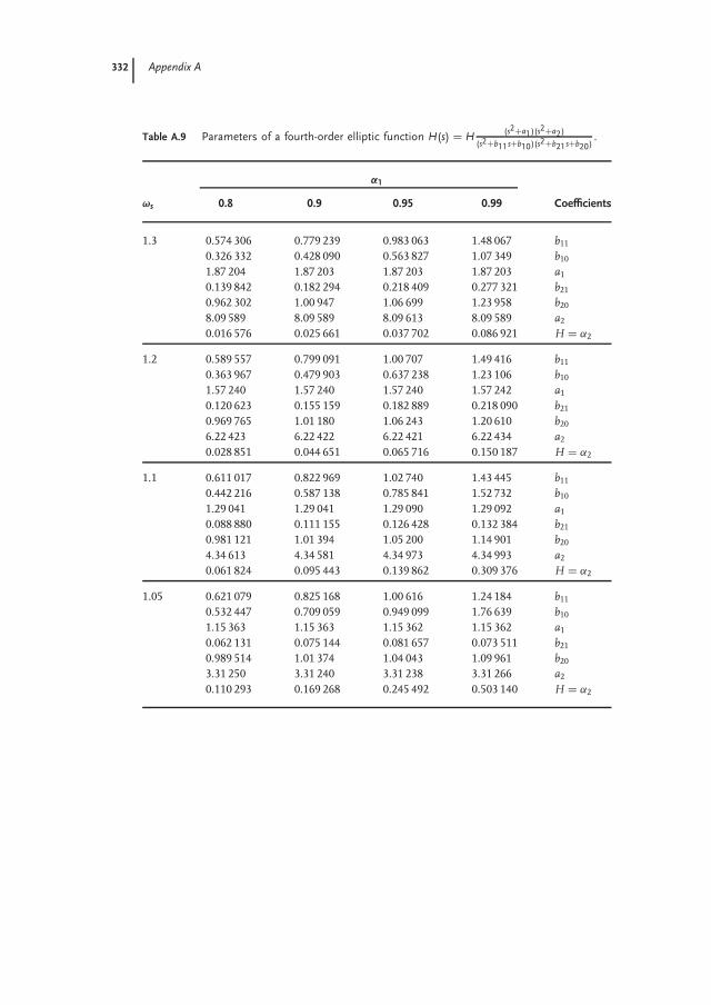
332 Appendix A
Table A.9 Parameters of a fourth-order elliptic function H(s) = H (s2+a1)(s2+a2)
(s2+b11s+b10)(s2+b21s+b20).
α1
ωs 0.8 0.9 0.95 0.99 Coefficients
1.3 0.574 306 0.779 239 0.983 063 1.48 067 b11
0.326 332 0.428 090 0.563 827 1.07 349 b10
1.87 204 1.87 203 1.87 203 1.87 203 a1
0.139 842 0.182 294 0.218 409 0.277 321 b21
0.962 302 1.00 947 1.06 699 1.23 958 b20
8.09 589 8.09 589 8.09 613 8.09 589 a2
0.016 576 0.025 661 0.037 702 0.086 921 H = α2
1.2 0.589 557 0.799 091 1.00 707 1.49 416 b11
0.363 967 0.479 903 0.637 238 1.23 106 b10
1.57 240 1.57 240 1.57 240 1.57 242 a1
0.120 623 0.155 159 0.182 889 0.218 090 b21
0.969 765 1.01 180 1.06 243 1.20 610 b20
6.22 423 6.22 422 6.22 421 6.22 434 a2
0.028 851 0.044 651 0.065 716 0.150 187 H = α2
1.1 0.611 017 0.822 969 1.02 740 1.43 445 b11
0.442 216 0.587 138 0.785 841 1.52 732 b10
1.29 041 1.29 041 1.29 090 1.29 092 a1
0.088 880 0.111 155 0.126 428 0.132 384 b21
0.981 121 1.01 394 1.05 200 1.14 901 b20
4.34 613 4.34 581 4.34 973 4.34 993 a2
0.061 824 0.095 443 0.139 862 0.309 376 H = α2
1.05 0.621 079 0.825 168 1.00 616 1.24 184 b11
0.532 447 0.709 059 0.949 099 1.76 639 b10
1.15 363 1.15 363 1.15 362 1.15 362 a1
0.062 131 0.075 144 0.081 657 0.073 511 b21
0.989 514 1.01 374 1.04 043 1.09 961 b20
3.31 250 3.31 240 3.31 238 3.31 266 a2
0.110 293 0.169 268 0.245 492 0.503 140 H = α2

333
Appendix B
B.1Bessel Thomson Filter Magnitude Error Calculations (MATLAB Program)
%BT filter magnitude error calculations h = ck;
nj = 1; end;
for n = 3:15; % if loop ends
nn = n-2; % BT polynomial is calculated
% as an iterative sum
for m = 1:45 bsum = blast +ck *x ^k1;
% variable of the BT polynomial is set blast = bsum;
y = 0.1 *m; end;
x = 0 +y *i; % k-loop ends
% calculations pertaining to ck begins bsum = blast;
n2 = 2 *n; % the BT transfer func value for a
% given ‘n’ and ‘x’ calculated
n1 = n +1; hs = h /bsum;
blast = 0; hsm = abs(hs);
for k = 1:n1 hsdb = -20 *log10(hsm);
k1 = k-1;% k1 goes from 0 to n ax(m) = y;
k2 = n2-k1;% means 2n-k1, k1 from 0 to n ay(nn,m) = hsdb;
k3 = n-k1;% means n-k1, k1 from 0 to n end;
% (2n-k1) ! loop begins %m-loop ends
fac1 = 1; end;
for l1 = 1:k2 % n-loop ends
facx = fac1 *l1; kk = linspace(1,13,13)
fac1 = facx; plot(ax,ay(kk,:),’w’)
end;% (2n-k1) ! loop ends axis([0 4.5 0 6])
faca = fac1; grid
%(n-k1) ! loop begins xlabel(’normalized frequency -->’)
fac2 = 1; ylabel(’magnitude error in dB’)
for l2 = 1:k3 text(1.8,4.5,’n = 3’)
(continued)
Modern Analog Filter Analysis and Design: A Practical Approach. Rabin Raut and M. N. S. SwamyCopyright 2010 WILEY-VCH Verlag GmbH & Co. KGaA, WeinheimISBN: 978-3-527-40766-8

334 Appendix B
facy = fac2 *l2; text(2.4,4.5,’4’)
fac2 = facy; text(2.6,4,’5’)
end;%(n-k1) ! loop ends text(2.9,3.8,’6’)
facb = fac2; text(3.1,3.7,’7’)
%k ! loop begins text(3.3,3.5,’8’)
fac3 = 1; text(3.5,3.4,’9’)
for l3 = 1:k1 text(3.6,3.3,’10’)
facz = fac3 *l3; text(3.7,3.1,’11’)
fac3 = facz; text(4.0,3.4,’12’)
end;%(k1 !) loop ends text(4.1,3.2,’13’)
facc = fac3; text(3.9,2.7,’14’)
%ck is computed text(4.1,2.6,’15’)
ck = faca /(facb *facc *2 ^k3); end
If k = = nj
%(contd. On next column)
B.2Bessel Thomson Filter Delay Error Calculations (MATLAB Program)
%BT filter delay calculations kev = kev-1;
% variable of the BT polynomial is set else
for nn = 1:13; bod = bodl-ck *(i) ^k *x ^k1;
n = nn +2; bodl = real(bod);
% m-loop begins odp = odpl-k1 *ck *(i) ^k *x ^(k1-1);
for m = 1:100 odpl = real(odp);
x = 0.1 *m; kev = kev +1;
% calculations pertaining to Ck begins end
n2 = 2 *n; % if-else loop ends
n1 = n +1; end
bevl = 0; bodl = 0; % k-loop ends
evpl = 0;odpl = 0; x1 = bevl;
Kev = 1; x2 = evpl;
% k-loop begins y1 = bodl;
for k = 1:n1 y2 = odpl;
k1 = k-1;% k1 goes from 0 to n anum = x1 *y2-y1 *x2;
k2 = n2-k1;% means 2n-k1, k1 from 0 to n den = x1 ^2 +y1 ^2;
k3 = n-k1;% means n-k1, k1 from 0 to n der = anum /den;
% (2n-k1) ! loop begins er = (1-der) /der;
fac1 = 1; ax(m) = x;
for l1 = 1:k2 ay(nn,m) = er *100;
facx = fac1 *l1; End
fac1 = facx; % m-loop ends
end;% (2n-k1) ! loop ends res1 = ax;
faca = fac1; res2 = ay;
%(n-k1) ! loop begins end
(continued)

B.2 Bessel Thomson Filter Delay Error Calculations (MATLAB Program) 335
fac2 = 1; % n-loop ends
for l2 = 1:k3 ax = res1;
facy = fac2 *l2; ay = res2;
fac2 = facy; plot(ax,ay,’w-’)
end;%(n-k1) ! loop ends axis([0 10 0 5])
facb = fac2; grid
%k ! loop begins xlabel(’normalized fequency -->’)
fac3 = 1; ylabel(’% delay error’)
for l3 = 1:k1 text(0.8,4.3,’n = 3’)
facz = fac3 *l3; text(2,4.3,’4’)
fac3 = facz; text(2.8,4.3,’5’)
end;%(k1 !) loop ends text(3.8,4.3,’6’)
facc = fac3; text(4.8,4.3,’7’)
%ck is computed text(5.7,4.3,’8’)
ck = faca /(facb *facc *2 ^k3); text(6.6,4.3,’9’)
% even part of BT polynomial is text(7.3,4.1,’10’)
calculated as an iterative sum
If kev = = 1 text(8.1,3.9,’11’)
bev = bevl +ck *(i) ^k1 *x ^k1; text(9,3.7,’12’)
bevl = real(bev); text(9.5,1.7,’13’)
evp = evpl +k1 *ck *(i) ^k1 *x ^(k1-1); text(9.5,.4,’14’)
evpl = real(evp); text(9.5,.1,’15’)
%(contd. On next column) end

337
Appendix C
C.1Element Values for All-Pole Single-Resistance-Terminated Low-Pass LosslessLadder Filters
In this section, we present the element values for all-pole LP single-resistance-terminated lossless ladder filters with Butterworth, Chebyshev, and Bessel– Thom-son approximations. Figures C.1a and C.1b correspond to voltage-driven structuresfor even- and odd-order filters, respectively, while Figures C.1c and C.1d tocurrent-driven structures for even- and odd-order filters, respectively. The elementvalues for several orders are given in Table C.1 for the Butterworth and Chebyshevfilters, and Table C.2 for the Bessel–Thomson filter. For other values of n andripple factors, one may refer to Weinberg (1962) and Huelsman (1993).
C.2Element Values for All-Pole Double-Resistance-Terminated Low-Pass LosslessLadder Filters
In this section, we present the element values for all-pole LP double-resistance-terminated lossless ladder filters with Butterworth, Chebyshev, and Bessel–Thomson approximations. Figures C.2a and C.2b correspond to structures foreven- and odd-order filters, respectively, while c and d are alternate structures foreven- and odd-order filters, respectively. The element values for several orders aregiven in Table C.3 for the Butterworth and Chebyshev filters, and Table C.4 forthe Bessel–Thomson filter. For other values of n and ripple factors in the case ofChebyshev filters, one may refer to Weinberg (1962) and Huelsman (1993).
Modern Analog Filter Analysis and Design: A Practical Approach. Rabin Raut and M. N. S. SwamyCopyright 2010 WILEY-VCH Verlag GmbH & Co. KGaA, WeinheimISBN: 978-3-527-40766-8

338 Appendix C
V1
I1
V1
I1
L2
C3 C1
C3 C1
Ln Ln′
L ′n−1 Ln−1
C ′n CnC ′2
L ′3 L ′1
L3′
L2
L1′
C2′C ′n−1Cn−1
+−
+−1
1
1
1
(a)
(c) (d)
(b)
Figure C.1 Low-pass single-resistance-terminated losslessall-pole ladder filters; (a) voltage-driven, even-order, (b)voltage-driven, odd order, (c) current-driven even-order, (d)current-driven odd order.
Table C.1 Element values for singly terminated losslessButterworth and Chebyshev filters (bandwidth normalized to1 rad s−1).
Order n C1 L2 C3 L4 C5 L6
Butterworth filter2 0.7071 1.41423 0.5000 1.3333 1.50004 0.3827 1.0824 1.5772 1.53075 0.3090 0.8944 1.3820 1.6944 1.54516 0.2588 0.7579 1.2016 1.5529 1.7593 1.5529
Chebyshev filter (0.5 dB ripple)2 0.7014 0.94033 0.7981 1.3001 1.34654 0.8352 1.3916 1.7279 1.31385 0.8529 1.4291 1.8142 1.6426 1.53886 0.8627 1.4483 1.8494 1.7101 1.9018 1.4042
Chebyshev filter (1.0 dB ripple)2 0.9110 0.99573 1.0118 1.3332 1.50884 1.0495 1.4126 1.9093 1.28175 1.0674 1.4441 1.9938 1.5908 1.66526 1.0773 1.4601 2.0270 1.6507 2.0491 1.3457
n L′1 C′
2 L′3 C′
4 L′5 C′
6

C.2 Element Values for All-Pole Double-Resistance-Terminated Low-Pass Lossless Ladder Filters 339
Table C.2 Element values for singly terminatedBessel–Thomson filter with a delay of 1 s at DC.
Order n C1 L2 C3 L4 C5 L6
2 0.3333 1.00003 0.1667 0.4800 0.83334 0.1000 0.2899 0.4627 0.71015 0.0667 0.1948 0.3103 0.4215 0.62316 0.0476 0.1400 0.2246 0.3005 0.3821 0.5595
n L′1 C′
2 L′3 C′
4 L′5 C′
6
Ln′ L3′ L1′
Cn′ −1
Cn′ Cn C3 C1
L2Ln′ −1 Ln−1L3′ L1′
C2′
C2′1
(a) (b)
(d)
Ln
1R
1
(c)
1/R R
Cn−1 C3 C1
L21/R
1
Figure C.2 Low-pass double-resistance-terminated lossless all-pole ladder filters.
Table C.3 Element values for doubly terminated losslessButterworth and Chebyshev filters (bandwidth normalized to1 rad s−1).
n C1 L2 C3 L4 C5 L6 C7
Butterworth filter2 1.4142 1.41423 1.0000 2.0000 1.00004 0.7654 1.8478 1.8478 0.76545 0.6180 1.6180 2.0000 1.6180 0.61806 0.5176 1.4142 1.9319 1.9319 1.4142 0.5176
Chebyshev filter (0.5 dB ripple)3 1.5963 1.0967 1.59635 1.7058 1.2296 2.5408 1.2296 1.70587 1.7373 1.2582 2.6383 1.3443 2.6383 1.2582 1.7373
Chebyshev filter (1.0 dB ripple)3 2.0236 0.9941 2.02365 2.1349 1.0911 3.0009 1.0911 2.13497 2.1666 1.1115 3.0936 1.1735 3.0936 1.1115 2.1666
n L′1 C′
2 L′3 C′
4 L′5 C′
6 L′7

340 Appendix C
Table C.4 Element values for singly terminatedBessel–Thomson filter with a delay of 1 s at DC.
Order n C1 L2 C3 L4 C5 L6
2 1.5774 0.42263 1.2550 0.5528 0.19224 1.0598 0.5116 0.3181 0.11045 0.9303 0.4577 0.3312 0.2090 0.07186 0.8377 0.4116 0.3158 0.2364 0.1480 0.0505
n L′1 C′
2 L′3 C′
4 L′5 C′
6
L1
L2′
C2′C3′
C4′C1′
L4′
Ln′
Cn′ −1
Ln′ −1
Cn′ −1
Cn′
L3 Ln−1
L n−1
Cn−1
Cn
C2C4
L2 L4
1
1/RL
RL
1/RL
For n Even For n Odd
For n Even For n Odd
Ln
1RL
(a)
(b)
Figure C.3 Elliptic LP double-resistance-terminated lossless filter structures.
C.3Element Values for Elliptic Double-Resistance-Terminated Low-Pass LosslessLadder Filters
In this section, we present the element values for elliptic LP double-resistance-terminated lossless ladder filters. Figure C.3a shows the structures for both even-and odd-order filters while Figure C.3b gives alternate structures for the filters.
Table C.5 provides element values for odd orders (3 and 5) and for even order (4)for the case when the response at infinite frequency is forced to zero by adopting amodified expression for the even order transfer function. In this transfer function,the denominator is of degree n while the numerator degree is forced to be n − 2.In this case, the load and source resistances are equal with a value of 1 each. Themodified elliptic function has the form

C.3 Element Values for Elliptic Double-Resistance-Terminated Low-Pass Lossless Ladder Filters 341
Tabl
eC
.5El
emen
tva
lues
for
the
ellip
ticfil
ter
ofFi
gure
C.3
aan
db.
nω
sA
aL 1
C2
L 2L 3
C4
L 4L 5
See
Figu
reC
.3a
31.
051.
748
0.35
550.
1537
45.
3959
60.
3555
1.1
3.37
40.
4462
60.
2699
32.
7035
30.
4462
61.
26.
691
0.57
336
0.44
981.
3080
50.
5733
64
1.05
3.28
40.
0044
20.
1722
14.
9376
41.
0122
40.
8444
51.
16.
478
0.17
279
0.32
758
2.30
986
1.04
894
0.89
415
(Pas
sban
dri
pple
0.1
dB)
1.2
12.0
850.
3713
90.
5663
81.
0929
41.
1193
80.
9244
05
1.05
13.8
410.
7081
30.
7663
00.
7357
21.
1276
10.
2013
84.
3811
60.
0498
51.
120
.050
0.81
296
0.92
418
0.49
338
1.22
445
0.37
193
2.13
500
0.29
125
1.2
28.3
030.
9144
11.
0651
60.
3162
81.
3820
10.
6013
11.
0932
90.
5297
4
31.
058.
134
1.05
507
0.25
223
3.28
904
1.05
507
1.1
11.4
801.
2252
50.
3747
11.
9475
21.
2252
51.
216
.209
1.42
450
0.52
544
1.11
977
1.42
450
41.
0511
.322
0.63
708
0.35
277
2.41
039
1.11
522
1.39
953
1.1
15.9
420.
8093
50.
5404
21.
4001
51.
1810
71.
4500
1(P
assb
and
ripp
le1.
0dB
)1.
222
.293
1.00
329
0.77
733
0.79
634
1.26
621
1.49
217
51.
0524
.134
1.56
191
0.67
560
0.83
449
1.55
460
0.26
584
3.31
881
0.88
528
1.1
30.4
711.
6969
10.
7751
10.
5882
71.
7989
20.
3992
21.
9890
71.
1210
91.
238
.757
1.82
812
0.87
005
0.38
720
2.09
095
0.56
347
1.16
672
1.38
094
nω
sA
aC
′ 1L′ 2
C′ 2
C′ 3
L′ 4C
′ 4C
′ 5Se
eFi
gure
C.3
b

342 Appendix C
Tabl
eC
.6A
ltern
ate
valu
esfo
rth
eel
liptic
filte
rsof
Figu
reC
.3a
and
b.
nω
sA
aL 1
C2
L 2L 3
C4
L 4L 5
C6
See
Figu
reC
.3a
41.
054.
485
0.15
780
0.18
091
4.73
822
1.20
743
0.82
637
1.10
8.30
80.
3341
10.
3343
82.
2833
31.
2688
10.
8482
71.
2014
.387
0.53
773
0.55
478
1.12
558
1.36
980
0.85
261
(Pas
sban
dri
pple
0.1
dB)R
L=
0.73
781
61.
0520
.307
0.57
153
0.65
752
1.01
346
0.92
972
0.32
584
2.72
744
1.03
524
0.88
809
1.10
27.8
890.
7078
30.
8170
30.
6799
21.
1048
40.
5189
01.
5464
01.
1977
90.
8852
31.
2037
.827
0.84
244
0.98
082
0.43
111
1.32
791
0.75
659
0.88
144
1.37
708
0.87
992
41.
0513
.243
0.95
111
0.26
779
3.20
104
1.90
749
0.80
699
1.10
18.1
401.
1623
90.
3995
81.
9107
72.
0522
80.
8090
71.
2024
.700
1.40
135
0.56
068
1.11
374
2.23
453
0.80
633
(Pas
sban
dri
pple
1.0
dB)R
L=
0.37
598
61.
0530
.730
1.40
432
0.58
067
1.14
761
1.37
588
0.31
837
2.79
144
1.79
883
0.82
259
1.10
38.3
421.
5690
60.
6914
90.
8033
51.
6683
20.
4560
91.
7593
71.
9978
60.
8207
61.
2048
.285
1.73
631
0.80
659
0.52
424
2.01
190
0.62
218
1.07
185
2.22
816
0.81
822
nω
sA
aC
′ 1L′ 2
C′ 2
C′ 3
L′ 4C
′ 4C
′ 5L′ 6
See
Figu
reC
.3b

C.3 Element Values for Elliptic Double-Resistance-Terminated Low-Pass Lossless Ladder Filters 343
HN (s) =Hc
n/2∏i=2
(s2 + 2i )
a0 + a1s + · · · + an−1s + ansn(C.3.1)
More details on this are available in Huelsman (1993).Table C.6 provides alternate set of element values for even orders (4 and 6),
where the modified elliptic transfer function has the same form as in Eq. (C.3.1),but the values of i are slightly different. The source and load resistances for thisalternate case are unequal with Rs = 1 .
In each of these tables only two values are used for Ap, namely, 0.1 and 1.0 dB.For a more exhaustive set of tables, refer to Huelsman (1993).

345
References
Abuelma’atti, M.T. and Shabra, A.M. (1966)A novel current-conveyor-based universalcurrent-mode filter. Microelectr. J., 27,471–475.
Ackerberg, D. and Mossberg, K. (1974) Aversatile active RC building block withinherent compensation for the finite band-width of the amplifier. IEEE Trans. CircuitsSyst., CAS-21, 75–78.
Al-Hashimi, B.M. and Fidler, J.K. (1988)New VCT-based active filter configura-tions and their applications. IEE SaragaColloquium on Electronic Filters, London,pp. 6/1–6/4.
Allen, P.E. and Sanchez-Sinencio, E. (1984)Switched Capacitor Circuits, Van NostrandReinhold Company, New York.
Altun, M. and Kuntman, H. (2008) De-sign of fully differential current modeoperational amplifier with improvedinput-output impedances and its filter ap-plications. AEU-Int. J. Electron. Commun.,62, 239–244.
Antoniou, A. (2006) Digital Signal Processing:Signals, Systems and Filters, McGraw-Hill.
Antoniou, A. (1967) Gyrators usingoperational amplifiers. Electron. Lett., 3,350–352.
Antoniou, A. (1969) Realization of gyratorsusing operational amplifiers and their usein RC-active network synthesis. Proc. Inst.Elec. Eng., 116, 1838–1850.
Assi, A., Sawan, M., and Raut, R. (1996)A new VCT for analog IC applications.Proc. Eighth International Conference onMicroelectronics, Cairo, pp. 169–172.
Assi, A., Sawan, M., and Raut, R. (1997)A fully differential and tunable CMOScurrent mode opamap based on
transimpedance-transconductance tech-nique. Proc. IEEE 40th Midwest Symp.Circuits and Systems, Sacramento, pp.168–171.
Bainter, J.R. (1975) Active filter has stablenotch, and response can be regulated.Electronics, 48, 115–117.
Baker, R.J., Li, H.W., and Boyce, D.E. (1998)CMOS Circuit Design, Layout and Simula-tion, IEEE Press.
Bermudez, J.C.M. and Bhattacharyya,B.B. (1982) Parasitic insensitivetoggle-switched capacitor and its appli-cation to switched-capacitor networks.Electron. Lett., 18, 734–736.
Bhattacharyya, B.B. and Swamy, M.N.S.(1971) Network transposition and itsapplication in synthesis. IEEE Trans.Circuit Theory, CT-18, 394–397.
Bhattacharyya, B.B., Sundaramurthy, M.,and Swamy, M.N.S. (1981) System-atic generation of canonic sinusoidalRC-active oscillators. IEE Proc. Part G, 128,114–126.
Biolek, D., Hancioglu, E., and Keskin,A.U. (2008) High-performancecurrent-differencing transconductanceamplifier and its application in precisioncurrent-mode realization. AEU-Int. J.Electron. Commun., 62, 92–96.
Bobrow, L.S. (1965) On active RC synthesisusing an operational amplifier. Proc. IEEE,53, 1648–1649.
Bruton, L.T. (1969) Network transfer func-tions using the concept of frequencydependent negative resistance. IEEE Trans.Circuit Theory, CT-16, 406–408.
Bruton, L.T. (1980) RC-Active Circuits Theoryand Design, Prentice Hall, Inc.
Modern Analog Filter Analysis and Design: A Practical Approach. Rabin Raut and M. N. S. SwamyCopyright 2010 WILEY-VCH Verlag GmbH & Co. KGaA, WeinheimISBN: 978-3-527-40766-8

346 References
Bruun, E. (1991) A differential-input,differential-output current mode oper-ational amplifier. Int. J. Electron., 71,1047–1056.
Bruun, E. (1994) A high-speed CMOS cur-rent opamp for very low supply voltageoperation. Proc. IEEE Int. Symp. Circuitsand Systems, London, pp. 509–512.
Carlosena, A. and Moschytz, G.S. (1993)Nullators and norators in voltage to cur-rent mode transformations. Int. J. CircuitTheory Appl., 21, 421–424.
Chang, C.M., Soliman, A.M., and Swamy,M.N.S. (2007) Analytical synthesis of lowsensitivity high-order voltage-mode DDCCand FDCCII-grounded R and C all passfilter structures. IEEE Trans. Circuits Syst. -Part I, 54, 1430–1443.
Chang, C.-M. (1991) Current mode all-pass/notch and bandpass filter usingsingle CCII. Electron. Lett., 27, 1812–1813.
Chang, C.-M. (1993) Universal active cur-rent filter with single input and threeoutputs using CCIIs. Electron. Lett., 29,1932–1933.
Chen, W.-K. (1990) Linear Networks andSystems: Algorithms and Computer-AidedImplementations, 2nd edn, vol. 1, WorldScientific Publishing Company Pvt. Ltd.
Chen, W.H. (1964) Linear Network Design andSynthesis, McGraw-Hill, New York.
Chen, W.-K. (1986) Passive and Active Filter,Theory and Implementations, John Wiley &Sons, Inc., New York.
Chen, W.-K. (Editor-in-Chief ) (1995) TheCircuits and Filters Handbook, Chapter 76,CRC Press.
Chen, H.P. (2009a) Versatile universalvoltage mode filter employing DDCCs.AEU-Int. J. Electron. Commun., 62, 78–82.
Chen, H.P. (2009b) Single FDCCII-baseduniversal voltage-mode filter. AEU-Int. J.Electron. Commun., 63, 713–719.
Cheng, K.H. and Wang, H.C. (1997) Designof current mode operational amplifier withdifferential input and differential output.Proc. IEEE Int. Symp. Circuits and Systems,Hong Kong, pp. 153–156.
Chiu, W.Y. and Horng, J.W. (2007)High-input and low-output impedancevoltage-mode universal biquadratic filterusing DDCCS. IEEE Trans. Circuits Syst.-Part II, 54, 649–652.
Christian, E. and Eisermann, E. (1977) FilterDesign Tables and Graphs, TransmissionNetworks International, Knightdale.
Daggett, K.E. and Vlach, J. (1969)Sensitivity-compensated active net-works. IEEE Trans. Circuit Theory, CT-16,416–422.
Darlington, S. (1939) Synthesis of reactance4-poles which produce prescribed insertionloss characteristics. J. Math. Phys., 18,257–353.
Deliyanis, T. (1968) High Q-factor circuitwith reduced sensitivity. Electron. Lett., 4,577.
Deliyanis, T., Sun, Y., and Fidler, J.K. (1999)Continuous-time Active Filter Design, CRCPress.
Director, S.W. and Rohrer, R.A. (1969) Thegeneralized adjoint network and networksensitivities. IEEE Trans. Circuit Theory,16, 318–323.
Elwan, H.O. and Soliman, A.M. (1996) Anovel CMOS current conveyor realizationwith an electronically tunable currentmode filter suitable for VLSI. IEEE Trans.Circuits Syst. - Part II, 43, 663–670.
Fabre, A. and Alami, M. (1995) Universalcurrent-mode biquad implemented from2nd generation current conveyors. IEEETrans. Circuits Syst. - Part I, 42, 383–385.
Fabre, A., Saaid, O., Wiest, F., andBoucheron, C. (1998) High-frequencyhigh-Q BiCMOS current-mode band-pass filter and mobile communicationapplication. IEEE J. Solid-State Circuits, 33,614–625.
Fan, S.C., Gregorian, R., Temes, G.C., andZomorodi, M. (1980) Switched capacitorfilters using unity gain buffers. Proc. IEEEInt. Symp. Circuits and Systems, Houston,pp. 334–337.
Fettweis, A. (1979a) Basic principles ofswitched capacitor filters using voltageinverter switches. AEU, 33, 13–19.
Fettweis, A. (1979b) Switched capacitor filtersusing voltage inverter switches: further de-sign principles. AEU, 33, 107–114.
Fettweis, A., Herbst, D., Hoefflinger, B.,Pandel, J., and Schweer, R. (1980) MOSswitched-capacitor filters using voltage in-verter switches. IEEE Trans. Circuits Syst.,CAS-27, 527–538.
Fleischer, P. and Tow, J. (1973) Design for-mulas for biquad active filters using three

References 347
operational amplifiers. Proc. IEEE, 61, pp.662–663.
Fleischer, P.E. and Laker, K.R. (1979) Afamily of active switched-capacitor biquadbuilding blocks. Bell Syst. Tech. J., 58,2235–2269.
Fried, D.L. (1972) Analog sampled data fil-ters. IEEE J. Solid-State Circuits, SC-7,302–304.
Friend, J.J. (1970) A single operational am-plifier biquadratic filter section. Proc. IEEEInt. Symp. Circuit Theory, Georgia, pp.179–180.
Friend, J.J., Harris, C.A., and Hilberman, D.(1975) STAR: an active biquadratic filtersection. IEEE Trans. Circuits Syst., CAS-22,115–121.
Geiger, R.L., Allen, P.E., and Strader, N.R.(1990) VLSI Design Techniques for Analogand Digital Circuits, McGraw-Hill.
Geiger, R.L. and Sanchez-Sinencio, E. (1985)Active filter design using operationaltransconductance amplifiers – a tutorial.IEEE Circuits Devices Mag., 1, 20–32.
Ghausi, M.S. and Laker, K.R. (1981) Mod-ern Filter Design – Active RC and SwitchedCapacitor, Prentice Hall, Inc.
Girling, F.E.J. and Good, F.F. (1970) Activefilters 12: the leap-frog or active-laddersynthesis. Wirel. World, 76, 341–345.
Gray, P.R. and Hodges, D.A. (1979) MOSswitched capacitor filters. Proc. IEEE, 67,61–75.
Gray, P.R. and Meyer, R.G. (1993) Analysisand Design of Analog Integrated Circuits,3rd edn, John Wiley & Sons, Inc.
Grebene, A.B. (1984) Bipolar and MOS Ana-log Integrated Circuit Design, John Wiley &Sons, Inc.
Gregorian, R. and Nicholson, W.E. (1979)CMOS switched capacitor filters for aPCM voice codec. IEEE J. Solid-StateCircuits, SC-14, 970–980.
Hakim, S.S. (1965) Active RC filters using anamplifier as the active element. Proc. IEE,112, 901–912.
Hodges, D.A., Gray, P.R., and Brodersen,R.W. (1978) Potential of MOS technolo-gies for analog integrated circuits. IEEE J.Solid-State Circuits, SC-13, 285–294.
Hokenek, E. and Moschytz, G.S. (1980)Analysis of general switched capacitor net-works using indefinite admittance matrix.Proc. IEE, Part G, 127, 21–33.
Huelsman, L.P. (1993) Active and passiveanalog filter design – An introduction,McGraw-Hill.
Hughes, J.B., Bird, N.C., and Macbeth, I.C.(1989) Switched currents- a new techniquefor analogue sampled-data signal process-ing. IEEE Int. Symp. Circuits and Systems,pp. 1584–1587.
Hughes, J.B., Macbeth, I.C., and Pattullo,D.M. (1990) Switched current filters. Proc.IEE, Part G, 137, 156–162.
Hurtig, G. III (1973) U.S. Patent 3,720,881.Hwang, Y.S., Wu, D.S., Chen, J.J., and Chou,
W.S. (2008) Realization of current-modehigh order filters employing multiple out-put OTAs. AEU-Int. J. Electron. Commun.,62, 299–303.
Ismail, M., Smith, S.V., and Beale, R.G.(1988) A new MOSFET-C universal filterstructure for VLSI. IEEE J. Solid-StateCircuits, SC-23, 183–194.
Jiraseree-amornkun, A. and Surakampotorn,W. (2008) Efficient implementation oftunable ladder filers using multi-outputcurrent controlled conveyors. AEU- Int. J.Electron. Commun., 62, 11–23.
Johns, D.A. and Martin, K. (1997) Analog In-tegrated Circuit Design, John Wiley & Sons,Inc.
Kerwin, W.J., Huelsman, L.P., andNewcomb, R.W. (1967) State variablesynthesis for insensitive integrated cir-cuit transfer functions. IEEE J. Solid StateCircuits, SC-2, 87–92.
Knob, A. (1980) Novel strays insensitiveswitched-capacitor integrator realizing thebilinear Z-transform. Electron. Lett., 16,173–174.
Kung, H.T. (1982) Why systolic architecture.Computer, 15, 37–46.
Kuo, B.C. (1967) Automatic Control System,Prentice Hall.
Kurth, C.F. and Moschytz, G.S. (1979)Nodal analysis of switched capacitor net-works. IEEE Trans. Circuits Syst., CAS-28,93–104.
Laker, K.R. and Sansen, W.M.C. (1994)Design of Analog Integrated Circuits andSystems, McGraw-Hill.
Laker, K.R. (1979) Equivalent circuits forthe analysis and synthesis of switchedcapacitor networks. Bell Syst. Tech. J., 58,729–769.

348 References
Laker, K.R. and Ghausi, M.S. (1980) Designof minimum sensitivity multiple-loopfeedback bandpass active filters. J. FranklinInst., 310, 51–64.
Li, R.D. and Raut, R. (2003) A VeryWide-Band OTA-C Filter in CMOS VLSITechnology. Proceedings of the 7th WorldMulticonference on Systemics, Cybernaticsand Informatics (SCI 2003), Orlando, Fl.,USA, paper#002396.pdf, pp. 1–6, (on CDROM).
Malawka, J. and Ghausi, M.S. (1980) Secondorder function realization with switchedcapacitor network and unity gain ampli-fiers. Proc. IEE, Part-G, 127, 187–190.
Mikhael, W.B. and Bhattacharyya, B.B. (1975)A practical design for insensitive RC-activefilters. IEEE Trans. Circuits Syst., CAS-22,407–415.
Minaei, S., Kuntman, H., and Cicekoglu,O. (2000) A new high output impedancecurrent-mode universal filter with singleinput and three outputs using dual outputCCIIs. Proc. 7th IEEE Int. Conf. Electron-ics, Circuits and Systems, Beirut, Lebanon,pp. 379–382.
Mitra, S.K. (1967) Transfer functionrealization using RC one-ports and twogrounded voltage amplifiers. Proc. FirstAnnual Princeton Conf. on Information Sci-ences and Systems, Princeton University,March 1967, pp. 18–23.
Mitra, S.K. (1969) Analysis and Synthesis ofLinear Active Networks, John Wiley & Sons,Inc.
Mohan, P.V.A. (2002) Current Mode AnalogVLSI Filters-Design and Implementation,Birkhauser.
Mohan, P.V.A., Ramachandran, V.,and Swamy, M.N.S. (1982) Generalstray-insensitive first-order active SCnetwork. Electron. Lett., 18, 1–2.
Mohan, P.V.A., Ramachandran, V., andSwamy, M.N.S. (1995) Switched Capac-itor Filters: Theory, Analysis and Design,Prentice Hall, London.
Moschytz, G.S. (1974) Linear IntegratedNetworks, Fundamentals, Van NostrandReinhold.
Moschytz, G.S. and Carlosena, A. (1994)A classification of current-mode sin-gle amplifier biquads based on avoltage-to-current transformation. IEEETrans. Circuits Syst. - Part II, 41, 151–156.
Nelin, B.D. (1983) Analysis of switched ca-pacitor networks using general purposecircuit simulation programmes. IEEETrans. Circuits Syst., CAS-30, 43–48.
Nguyen, N.M. and Meyer, R.G. (1990)Si-IC-compatible inductors and LC pas-sive filters. IEEE J. Solid-State Circuits, 25,1028–1031.
Orchard, H.J. (1966) Inductorless filters. Elec-tron. Lett., 2, 224–225.
Patel, V. and Raut, R. (2008) A study onCMOS negative resistance circuits. Proc.IEEE Canadian Conf. Electrical and Com-puter Engineering, pp. 1.283–1.288.
Prasad, D., Bhaskar, D.R., and Singh, A.K.(2009) Universal current-mode biquad fil-ter using dual output current differencingtransconductance amplifier. AEU-Int. J.Electron. Commun., 63, 497–501.
Raut, R. (1992) A novel VCT for analog ICapplications. IEEE Trans. Circuits Syst. -Part II, 39, 882–883.
Raut, R. (1993) A voltage to current trans-ducer (VCT) in CMOS technology forapplications in analog VLSIC. Proc.Canadian Conf. Electrical and ComputerEngineering, Vancouver, pp. 82–85.
Raut, R. and Daoud, N.S. (1993)Current-mode oscillator realization us-ing a voltage-to-current transducer inCMOS technology. Proc. IEE, Part-G, 140,462–464.
Raut, R. (1984) Some design and analysistechniques for practical sc sampled datafilters using unity gain amplifiers. Ph.D.Thesis, Concordia University, Montreal.
Raut, R. and Bhattacharyya, B.B. (1984a) Anote on the analysis of multiphase SC net-works containing operational amplifiers.Proc. International Conf. on Computers,Systems and Signal Processing, Bangalore,pp. 1400–1403.
Raut, R. and Bhattacharyya, B.B. (1984b) De-sign of parasitic tolerant switched-capacitorfilters using unity-gain buffers. Proc. IEE,Part-G, 131, 103–113.
Raut, R., Bhattacharyya, B.B., and Faruque,S.M. (1992) Systolic array architectureimplementation of parasitic-insensitiveswitched-capacitor filters. Proc. IEE,Part-G, 139, 384–394.
Raut, R. and Guo, N. (1997) Low powerwide band voltage and current mode sec-ond order filters using wide band CMOS

References 349
transimpedance network. Proc. IEEE Int.Symp. Circuits and Systems, Hong Kong,pp. 313–316.
Raut, R., Swamy, M.N.S., and Tian, N.(2007) Current mode filters using voltageamplifiers. Circuits, Syst. Signal Process.,26, 773–792.
Roberts, G.W. and Sedra, A.S. (1989) All cur-rent mode selective circuits. Electron. Lett.,25, 759–761.
Roberts, G.W. and Sedra, A.S. (1992) Ageneral class of current amplifier-basedbiquadratic filter circuits. IEEE Trans.Circuits Syst. - Part I, 39, 257–263.
Ruston, H. and Bordogna, J. (1971) Electri-cal Networks: Functions, Filters, Analysis,McGraw-Hill.
Sallen, R.P. and Key, E.L. (1955) A practicalmethod of redesigning RC-active filters.IEEE Trans. Circuit Theory, CT-2, 74–85.
Sanchez-Sinencio, E., Geiger, R.L., andNevarez-Lozano, H. (1998) Generation ofcontinuous-time two integrator loop OTAfilter structures. IEEE Trans. Circuits Syst.,CAS-35, 936–946.
Schaumann, R. and Van Valkenburg, M.E.(2001) Design of Analog Filters, OxfordUniversity Press.
Schaumann, R., Ghausi, M.S., and Laker,K.R. (1990) Design of Analog Filters: Passive,Active RC, and Switched Capacitor, PrenticeHall, Englewood Cliffs.
Sedra, A.S., Smith, K.C. (1970) A secondgeneration current conveyor and its appli-cations. IEEE Trans. Circuit Theory, CT-17,132–134.
Sedra, A.L. and Smith, K.C. (2004) Microelec-tronic Circuits, 5th edn, Oxford UniversityPress.
Sedra, A.S. and Brackett, P.O. (1978) Fil-ter Theory and Design: Active and Passive,Matrix Publishers, Inc.
Senani, R. (1992) New current-mode biquadfilters. Int. J. Electron., 73, 735–742.
Soliman, A.M. (1996) Applications of currentfeedback operational amplifiers. Analog In-tegr. Circ. Signal Process., 11, 265–302.
Soliman, A.M. (1997) New current modefilters using current conveyors. AEU-Int. J.Electron. Commun., 51, 275–278.
Su, K.L. (1996) Analog Filters, Chapman &Hall.
Sun, Y. and Fidler, J.K. (1995) High-ordercurrent-mode continuous-time multiple
output OTA capacitor filters. IEE 15thSARAGA Colloquium on Digital and Ana-logue Filters and Filtering Systems, London,1995, pp. 8/1–8/6.
Sun, Y. and Fidler, J.K. (1996) Structuregeneration of current-mode two integratorloop dual output-OTA grounded capacitorfilters. IEEE Trans. Circuits Syst. - Part II,43, 659–663.
Sun, Y. and Fidler, J.K. (1997) Structuregeneration and design of multiple loopfeedback OTA-grounded capacitor filters.IEEE Trans. Circuits Syst. - Part I, 44,1–11.
Swamy, M.N.S. (1975) Modern Filter Design,Classroom Notes, Department of Electricaland Computer Engineering, ConcordiaUniversity, Montreal.
Swamy, M.N.S., Bhusan, C., andBhattacharyya, B.B. (1974) Generalizedduals, generalized inverses and theirapplications. J. Inst. Electron. Rad. Eng., 44,95–99.
Swamy, M.N.S., Bhusan, C., andBhattacharyya, B.B. (1976) Generalizeddual transposition and its applications. J.Franklin Inst., 301, 465–476.
Swamy, M.N.S. and Thulasiraman, K. (1981)Graphs, Networks and Algorithms, JohnWiley-Interscience, New York.
Swamy, M.N.S., Bhusan, C., andThulasiraman, K. (1972) Sensitivity in-variants for active lumed/distributednetworks. Electron. Lett., 8, 26–29.
Swamy, M.N.S., Raut, R., and Tang, Z.(2004) Generation of new OTA-C oscillatorstructures using network transposition.Proc. IEEE 47th Midwest Symposium onCircuits and Systems, Hiroshima, 1, pp.73–76.
Swamy, M.N.S. and Raut, R. (2002) Real-ization of gm-C current-mode filters fromassociated gm-C voltage-mode filters. Proc.IEEE 45th Midwest Symposium on Cir-cuits and Systems, Tulsa, Oklahoma, 2, pp.625–628.
Szczepansky, S. Jakusz, J., and Schaumann,R. (1997) A linear fully balanced CMOSOTA for VHF filtering applications. IEEETrans. Circuits Syst. - Part II, 44, 174–187.
Tang, Z. (2004) Application of network trans-position in the design of OTA-C filters andoscillators, M.A.Sc. Thesis, Concordia Uni-versity.

350 References
Tangsrirat, W., Tanjaroen, W., andPukkalamm, T. (2009) Current-modemultiphase sinusoidal oscillator usingCDTA-based all pass sections. AEU-Int. J.Electron. Commun., 62, 616–622.
Temes, G.C. and Mitra, S.K. (1973) ModernFilter Theory and Design, John Wiley &Sons, Inc., New York.
Thomas, R.E. (1959) Technical Note No.8, Circuit Theory Group, University ofIllinois, Urbana.
Thomas, L.C. (1971a) The biquad: part I- some practical design considerations;part II-a multipurpose active filtering sys-tem. IEEE Trans. Circuit Theory, CT-18,350–357.
Thomas, L.C. (1971b) The Biquad: part II - amultipurpose active filtering system. IEEETrans. Circuit Theory, CT-18, 358–361.
Thomson, W.E (1949) Delay networks havingmaximally flat frequency characteristics.Proc. IEE, (part 3), vol. 96, 487–490.
Tow, J. (1968) Active RC filters – a statespace realization. Proc. IEEE, 56, 87–92.
Tow, J. (1969) A step-by-step active filterdesign. IEEE Spectr., 6, 64–68.
Tsividis, Y., Banu, M., and Khoury, J. (1986)Continuous-time MOSFET-C filters inVLSI. IEEE Trans. Circuits Syst., CAS-33,125–140.
Toumazou, C., Lidgey, J., and Haigh, D.(eds) (1990) Analogue IC Design – The
Current-Mode Approach, IEE Press,London.
Tu, S.H., Chang, C.M., Ross, N.J.,and Swamy, M.N.S. (2007) Ana-lytical synthesis of current-modehigh-order single-ended-input OTA andequal-capacitor elliptic filter structureswith the minimum number of compo-nents. IEEE Trans. Circuits Syst. - Part I,54, 2196–2210.
Van Valkenburg, M.E. (1960) Introduction toModern Network Synthesis, John Wiley &Sons, Inc.
Vandewalle, J., DeMan, H.J., and Rabey, J.(1981) Time, frequency and z-Domainmodified nodal analysis of switched capac-itor networks. IEEE Trans. Circuits Syst.,CAS-28, 186–195.
Wang, C., Zhou, L., and Li, T. (2008) A newOTA-C current-mode biquad with singleinput and multiple outputs. AEU-Int. J.Electron. Commun., 62, 232–234.
Weinberg, L. (1962) Network Analysis andSynthesis, McGraw-Hill, New York.
Yanagisawa, T. (1957) RC active networksusing current inversion type negativeimpedance converters. IEEE Trans. CircuitTheory, CT-4, 140–144.
Zverev, A.L. (1967) Handbook of Filter Synthe-sis, John Wiley & Sons, Inc.

351
Index
aAckerberg-Mossberg biquad see under biquadactive building blocks 28, 41, 147, 161, 265active devices 4, 5, 28, 103, 124, 126, 143,
191, 192, 207, 214, 228, 268, 283, 299, 300,304
active resistor see under resistoractive RC filters 1, 4, 28, 30, 43, 103, 217,
221, 223, 299, 304adjoint network 268admittance matrix 9, 13, 15, 18alias 168All-pass filter 53, 108, 155, 265all-pole function 4, 56, 65, 85, 89, 230, 233all-pole filter 88, 217anti-aliasing filter 168analog filters 4, 7, 28, 30, 148, 161, 299,
300, 302Antoniou’s GIC 209, 210, 214, 251approximation 4, 5, 41– magnitude see magnitude approximation– phase see phase approximation– constant-delay see constant delay
approximation
bband-pass filter 30, 31, 115, 138, 154–157,
160, 172, 206, 222, 265, 321band-reject filter 4, 53band-stop filter see band-reject filterbandwidth 3, 71, 73, 76, 108, 168, 172, 285,
314Bessel polynomial 75Bessel-Thomson (BT) filters 5, 75–77, 328,
329, 333–335, 339, 340bilinear transformation see under
transformationbiquadratic filter 103–105, 187–178–189, see
also biquads and second order filters
biquadratic function 104, 199, 229biquads 103–105, see also biquadratic filters
and second order filters– Ackerberg-Mossberg 156, 282– Fleischer–Tow 123, 273, 274– KHN see under KHN state variable filter– Mikhael-Bhattacharyya 126– single amplifier 109–117– Tow-Thomas 121, 132, 223, 281brick-wall characteristics 41, 53Bruton’s transformation see under
transformationButterworth approximation see under
magnitude approximationButterworth filter 56, 58, 59, 91, 95, 96, 99,
100, 232, 236, 237, 327, 337, 338, 339
ccapacitive dual 45–47, 79, 269, 270, 295cascade 16, 23, 46, 129, 193, 202, 220, 225,
227, 228, 229, 239, 245, 248, 250, 258, 270,319
Cauer networks 86–88, 90, 95, 97, 100CCII see Current conveyor IICCCS see Current controlled current sourceCCVS see Current controlled voltage sourcechain matrix 14–16, 42, 45–49, 89,
208–211chain parameters 14Chebyshev approximation see under
magnitude approximationChebyshev filter 65, 95, 328, 329, 337, 338,
339clock feed-through 174, 291, 302clock frequency 162, 163, 167, 187CMOS 2, 3, 5, 144, 147, 264, 266, 285, 318,
323
Modern Analog Filter Analysis and Design: A Practical Approach. Rabin Raut and M. N. S. SwamyCopyright 2010 WILEY-VCH Verlag GmbH & Co. KGaA, WeinheimISBN: 978-3-527-40766-8

352 Index
component simulation 207–209, 211–213,215
component transformation 96constant delay approximation 75–77constrained networks 4, 7, 24–27, 110, 117continued fraction (CF) expansion 86, 87,
90, 91continuous-time domain 207, 251continuous-time filters 2, 5, 138, 150controlled sources 7, 16, 17, 24, 48, 52, 268,
280current controlled current source (CCCS)
7, 16, 17, 18, 28, 31, 42, 48, 49, 79, 80, 113,114, 256, 258, 262, 271, 272, 280, 283
current controlled voltage source (CCVS)7, 16, 17, 18, 48, 49, 79, 80, 262, 294
current conveyor II (CCII) 3, 7, 31, 32, 114,151, 257, 261–266, 294, 320–322
controlled currect conveyor II (CCCII) 114,319–322
current amplifier 261, 269, 270, 271current copier 285current mirror 32, 149, 256, 285, 287, 291current OA 114, 151current-mode (CM) filters 3, 33, 150,
255–294, 345–347current transfer function (CTF) 3, 12, 32,
36, 43, 46, 47, 48, 49, 52, 80, 84, 85, 93,214, 265, 267, 268, 271, 272, 273, 274, 275,276, 278, 279, 281, 282, 283, 284, 285
current transfer function (CTF) matrix 271,276, 277, 295
CTF matrix see current transfer function(CTF) matrix
cut-off frequency 53, 54, 60, 69, 90, 91, 92,221, 225, 226
dD-network 201, 202delay 53, 54, 68, 74, 75delay and add 200–203delay equalizers 53, 55, 77differential architecture 5, 303differential structure 303–307, 310–312,
316, 323differential input OTA 277diffused resistor see under resistordigital filters 3, 192, 200discrete-time equations 163, 175, 178differential-input single-output (DISO)-OTA
277–279doubly-terminated LC ladder 4, 92–100,
214
doubly-terminated network 50, 51, 83, 93,252
driving point admittance 12, 86, 110driving point function 48, 271driving point impedance (DPI) 12, 42, 46,
50, 86, 94, 208, 210, 211, 214, 268dual one-port 44, 45dual networks 5, 44, 45, 270, 271, also see
capacitive, resistive and generalized dualsdual transpose 50dual two-port 4, 45, 47, 49, 50, 51, 79, 85, 94,
97, 100, 269, 270, 271, also see capacitivedual
dynamic current mirrors 285dynamic range equalization 147, 191, 198,
207, 228, 229, 314
eelliptic approximation see under magnitude
approximationelliptic filter 67, 68, 223, 249, 330, 311, 332epitaxial and ion-implanted resistors 143equivalent networks 16, 30equal-ripple (equi-ripple) 62
ffeature size 147, 323feed-forward technique 122FDNR 208, 211, 213–217, 250, 252, 253filter functions 5, 41, 122, 304, 319floating inductor 208–210, 212, 215Fleischer–Tow see under biquadforward open circuit voltage gain 15forward short circuit current gain 15forward transconductance 15frequency-dependent negative resistor see
FDNRfrequency domain characterization 7, 163,
167frequency scaling 51, 62, 64, 96frequency transformations see under
transformation– low-pass to band-pass see under
transformation– low-pass to high-pass see under
transformation– low-pass to band-reject (bandstop) see under
transformation
ggain-bandwidth (GB) product 132, 134, 147,
284, 285– effects of finite GB of an OA 283

Index 353
generalized dual 45, 46, 47, 49, 255, 268, 269,also see dual two-ports and capacitive dual
generalized immittance converter 210, 211general network theorems 41gm-C filter see OTA-C filtergrounded inductance 212, 321gyrator 138, 208–210, 214, 239, 255, 263
hhigh-pass filter 4, 53, 108, 115, 160higher order active filters 207–251Hurwitz polynomial 89hybrid technology 141
iideal operational amplifier (OA) 101, 105,
128, 131, 132, 134, 224, 226, 280immittance 210, 211impedance converter 7, 17, 18, 33, 49, 80,
210, 268impedance inverter 7, 17, 18, 48, 49, 138, 208,
263, 268, 271, 294, see also gyratorimpedance matrix 11, 14, 15, 48impedance scaling 41–43impedance transformation see under
transformationindefinite admittance matrix (IAM) 18–23,
39, 41inductance simulation 5, 208, 210, 239integrators– ideal 241– inverting 30, 181, 183, 184, 196, 220, 231,
233, 234, 246, 247, 292Lossy 29, 106, 177, 181, 220, 221, 230, 231,
233, 260, 308, 310, 312, 316Noninverting 181, 183, 196, 220, 304, 306inverse Chebyshev approximation see under
magnitude approximationinverse follow the leader feedback (IFLF)– structure 238inverse network 44, 45, see also dual two-port
network
kKHN state variable filter 119–121, 127, 128
lladder filter 33, 101, 212, 214, 215, 222, 224,
239, 245, 250–252leapfrog structure 217, 220, 221, 242, 243,
278, 279, 297linear phase approximation see constant delay
approximationlinear phase 75, 78
loop analysis 7–11lossless digital integrator (LDI)– transformation see under transformationlossless integrator 106, 177, 179, 230, 290,
307, 316lossless (LC) ladder filter 50, 88, 90, 92, 100,
207, 208, 212, 213, 214, 217, 245, 250,337–341
lossless ladder simulation 207, 212,213–216, 217–225, 239–245, 250
lossless network 80, 83, 89, 93, 94lossy integrator 29, 106, 177, 181, 220, 230,
231, 233, 260, 308, 310, 312, 316inverting 29, 106, 177, 181, 220, 221, 232,
233, 236, 308Noninverting 177, 181, 186, 220low-pass (LP) filter 4, 31, 33, 35, 154–156,
160, 204, 206, 240, 253, 337, 340low-pass to band-pass transformation see
under transformationlow-pass to high-pass transformation see
under transformationlow-pass to band-reject (bandstop)– transformation see under transformation
mmagnitude approximation 54–69– Butterworth 56– Chebyshev 60–65– – maximally flat magnitude (MFM)
55–60– elliptic 65–68– inverse Chebyshev 68MATLAB 4, 5, 58, 59, 64, 65, 68, 76, 171,
173, 300maximum power transfer 50mesh analysis see loop analysisMikhael-Bhattacharyya biquad see under
biquadmimimum sensitivity feedback structure
238MFM approximation see under magnitudeapproximationmodified leap-frog (MLF) structure
238modular approach 191–194monolithic inductor 3, 147MOS switch 175, 184MOS capacitor 144–146, 175multi-in single-output (MISO) system
122, 123multiple amplifier biquad 117–128multiple feedback 5, 207–237

354 Index
nnegative impedance converter (NIC) 17, 18– current inverting 17, 21, 22, 80, 263, 267– voltage inverting 17, 267negative impedance inverter (NII) 17, 18,
263, 294network function 7, 12, 18, 138, 139, 154,
190, 213, 217network transposition see transpositionnodal analysis 8, 9, 11noise signal 303nonreciprocal network 7, 15, 16, 18, 48, 271nodal admittance matrix 18, 19noninverting amplifier 131, 132, 238notch filter 55, 140, 265, 266– highpass notch 108, 109, 157– lowpass notch 108, 109, 157– symmetric 108, 109null filter see notch filternullator 268, 279, 280
oone-pole model 147, 184one-port network 12, 16, 44, 45, 85, 94OA see operational amplifieropen circuit impedance parameters 14operational amplifier 24–26, 28, 29, 30,
105–107, 147, 148, 258operational simulation technique 5, 217,
219–224, 239, 241, 253operational transconductance amplifier
(OTA) 2, 30, 31, 135, 139, 149, 239,241, 243
OTA-C filters 5, 138, 139, 159, 310,312, 314
pparasitic capacitances 2, 138, 145, 159, 161,
174–176, 204, 239, 245, 260, 270, 285,301–303, 310, 312, 313
parasitic-insensitive structures see underswitched-capacitor (SC) filter
passband 41, 50, 53, 54, 55, 56, 60, 61, 63,67, 68, 69, 71, 73, 96, 227, 228
phase approximation 73–77phase delay 74pinched resistor see under resistorpole frequency 104pole zero pairing 228, 229pole-Q 104positive impedance converter (PIC) 17positive impedance inverter (PII) 18, 138,
208, see also gyrator
prewarping 170–172, 205, 248, 250, 251,293
primary resonator block (PRB) 237
qQuality factor (Q) 71, 211, 285Q−enhancement 134Qp-sensitivity see under sensitivity
rrational function 29, 50, 66RC:CR transformation see under
transformationreactance function 85, 86, 87, 89, 90reactance network 85, 86reciprocal network 15, 47, 48, 100reconstruction filter 168reflection coefficient 94resistive dual 45, also see dual networksresistor– active 143– diffused 142– pinched 142reversed two-port (network) 47, 48
sSallen and Key filters 110–116sampled-data domain 164, 166, 170, 207,
250, 251, 289sampled-data frequency 163, 168–170sampled-data transfer function 167–169– Frequency domain characteristics of 167second-order filters 4, 7, 30, 31, 35, 52,
103–140, 157, 159, 161, 181, 187, 189, 191,193, 195, 197, 207, 223, 225, 239, 253, 266,278, 280, see also biquadratic filters andbiquads
sensitivity 4, 124–127, 129, 154, 207, 213,216, 227–229, 238, 267, 272, 300
Qp-sensitivity 125, 126, 127, 267ωp-sensitivity 126, 127shifted-companion feedback structure 235short circuit admittance parameters 13signal-flow graph technique 192–198Silicon dioxide 144–146simulation of LC ladder 217single-amplifier biquad see under biquadsingle-input dual-output (SIDO) OTA
277–279single-input multi-output (SIMO) 121singly terminated network 50, 51, 83, 84,
90–92source transformation 9–11, 239, 240state variable filter 119, 120, 126, 127

Index 355
stopband 41, 53, 54, 55, 63, 66, 67, 68, 69,71, 72, 170,
super-capacitors 213, 215, 217, also see FDNRswitched-capacitor (SC) filter 2, 149,
161–206– parasitic insensitive (PI) 4, 162, 175–187,
245–250– second-order 162, 192, 196– higher-order 248, 249swiched-current filters see switched-current
techniquesswitched-current techniques 285–294switched-current memory 286systolic array architecture 192
ttime-delay see delaythree-terminal two-port 16threshold voltage 144, 291, 301topological dual 45Tow-Thomas biquad see under biquadtransadmittance function (TAF) 12, 52, 84,
92, 118transconductance 51, 135, 149, 260transconductance amplifier 150, 258transconductance-C filter see OTA-C filtertransformation– bilinear (s→z) 161, 169–173– Bruton’s 214– Frequency 69–71, 114– impedance 42–43, 113–114, 214, 217– lossless digital integrator (LDI) 166– low-pass to band-pass 71, 88, 237, 316– low-pass to high-pass 69–70, 212– low-pass to band-reject (bandstop) 73– RC:CR 79, 113–115transimedance amplifier 258transimedance function (TIF) 12, 15, 52,
84, 89, 93transition band 53, 54, 67, 68, 69, 72, 168transmission parameters see chain
parameterstransmission zero 66, 88, 89, 128, 215, 223,
230, 233, 237transposed networks 4, 48, 50, 268, 271,
273, 280
transposition 3, 5, 267, 268, 271–273, 275,277, 279, 295
two-port networks 4, 7, 12, 13, 15–17, 22,37, 41, 42, 45, 48, 268
two-port parameters 4, 13–18
uunity gain amplifier (UGA) 105, 199–204
vVCCS see Voltage controlled current sourceVCVS see Voltage controlled voltage sourceVLSI 2, 303voltage amplifier 25–29, 105, 109, 117, 131,
137, 185, 199, 269, 307voltage controlled current source (VCCS) 7,
16, 17, 18, 28, 30, 48, 49, 79, 80, 262, 271voltage controlled voltage source (VCVS) 7,
16–18, 24, 26, 28, 29, 34, 42, 48, 49, 79,113, 114, 184–186, 217, 262, 268, 271, 272,280–283
voltage follower 105voltage mode (VM) 5, 103, 217, 225, 255,
267–279voltage transfer function (VTF) 12, 32, 35,
39, 43, 46–49, 52, 80, 84, 85, 93, 214, 265,267, 268, 271–283, 285, 294, 295
VTF see votage transfer functionvoltage transfer function (VTF) matrix 271,
276, 295VTF matrix see voltage transfer function
(VTF) matrix
wwarping 170
yy-parameters see short circuit admittance
parameters
zz-parameters see open circuit impedance
parametersz-transform 163–165, 178, 179