
Analog electronic Circuits - Alpha College of...
178
Analog electronic Circuits 1 University syllabus Module-1 Diode Circuits: Review of diodes as rectifiers (No question shall be set from review portion). Diode clipping and clamping circuits. Transistor biasing and stabilization: Operating point, analysis and design of fixed bias circuit, self-bias circuit, Emitter stabilized bias circuit, voltage divider bias circuit, stability factor of different biasing circuits. Problems. Transistor switching circuits: Transistor switching circuits, PNP transistors, thermal compensation techniques. Module-2 Transistor at low frequencies: BJT transistor modelling, CE fixed bias configuration, voltage divider bias, emitter follower, CB configuration, collector feedback configuration, analysis using h – parameter model, relation between h – parameters model of CE, CC and CB modes, Millers theorem and its dual. Transistor frequency response: General frequency considerations, low frequency response, Miller effect capacitance, high frequency response, multistage frequency effects. Module-3 Multistage amplifiers: Cascade and cascode connections, Darlington circuits, analysis and design. Feedback amplifiers: Feedback concept, different types, practical feedback circuits, analysis and design of feedback circuits. Module-4 Power amplifiers: Amplifier types, analysis and design of different power amplifiers, distortion in power amplifiers. Oscillators: Principle of operation, analysis and derivation of frequency of oscillation of phase shift oscillator, Wien bridge oscillator, RF and crystal oscillator and frequency stability. Module-5 FETs: Construction, working and characteristics of JFET and MOSFET. Biasing of JFET and MOSFET, JFET and MOSFET amplifiers, analysis and design.
Transcript of Analog electronic Circuits - Alpha College of...

Analog electronic Circuits 1
University syllabusModule-1
Diode Circuits: Review of diodes as rectifiers (No question shall be set from review portion).Diode clipping and clamping circuits.
Transistor biasing and stabilization: Operating point, analysis and design of fixed bias circuit,self-bias circuit, Emitter stabilized bias circuit, voltage divider bias circuit, stability factor ofdifferent biasing circuits. Problems.Transistor switching circuits: Transistor switching circuits, PNP transistors, thermalcompensation techniques.
Module-2Transistor at low frequencies: BJT transistor modelling, CE fixed bias configuration, voltagedivider bias, emitter follower, CB configuration, collector feedback configuration, analysis using h
– parameter model, relation between h – parameters model of CE, CC and CB modes, Millers theorem and its dual.Transistor frequency response: General frequency considerations, low frequency response, Miller effect capacitance, high frequency response, multistage frequency effects.
Module-3Multistage amplifiers: Cascade and cascode connections, Darlington circuits, analysis and design.Feedback amplifiers: Feedback concept, different types, practical feedback circuits, analysis anddesign of feedback circuits.
Module-4Power amplifiers: Amplifier types, analysis and design of different power amplifiers, distortion in power amplifiers.Oscillators: Principle of operation, analysis and derivation of frequency of oscillation of phase shift oscillator, Wien bridge oscillator, RF and crystal oscillator and frequency stability.
Module-5FETs: Construction, working and characteristics of JFET and MOSFET. Biasing of JFET and MOSFET, JFET and MOSFET amplifiers, analysis and design.

Analog electronic Circuits 2
Table of Contents
Sl.No Modules Page no.
1 Diode circuits and transistor biasing 03
2 Transistor at low frequency and 53frequency response
3 Multistage amplifier and feedback 77amplifier
4 Power amplifier and oscillator 98
5 FETs 146

Analog electronic Circuits 3
Module-1
Diode circuits
Diode:
A pure silicon crystal or germanium crystal is known as an intrinsic semiconductor. There are notenough free electrons and holes in an intrinsic semi-conductor to produce a usable current. Theelectrical action of these can be modified by doping means adding impurity atoms to a crystal toincrease either the number of free holes or no of free electrons.
When a crystal has been doped, it is called a extrinsic semi-conductor. They are of two types
• n-type semiconductor having free electrons as majority carriers
• p-type semiconductor having free holes as majority carriers
By themselves, these doped materials are of little use. However, if a junction is made by joining p-type semiconductor to n-type semiconductor a useful device is produced known as diode. It willallow current to flow through it only in one direction. The unidirectional properties of a diodeallow current flow when forward biased and disallow current flow when reversed biased. This iscalled rectification process and therefore it is also called rectifier.
How is it possible that by properly joining two semiconductors each of which, by itself, will freelyconduct the current in any direct refuses to allow conduction in one direction.
Consider first the condition of p-type and n-type germanium just prior to joining fig. 1 . Themajority and minority carriers are in constant motion.
The minority carriers are thermally produced and they exist only for short time after which theyrecombine and neutralize each other. In the mean time, other minority carriers have beenproduced and this process goes on and on.
The number of these electron hole pair that exist at any one time depends upon the temperature.The number of majority carriers is however, fixed depending on the number of impurity atomsavailable. While the electrons and holes are in motion but the atoms are fixed in place and donot move.

Analog electronic Circuits 4
Holes from the p-side diffuse into n-side where they recombine with free electrons.Free electrons from n-side diffuse into p-side where they recombine with free holes.
The diffusion of electrons and holes is due to the fact that large no of electrons are concentratedin one area and large no of holes are concentrated in another area.
When these electrons and holes begin to diffuse across the junction then they collide each otherand negative charge in the electrons cancels the positive charge of the hole and both will losetheir charges.
The diffusion of holes and electrons is an electric current referred to as a recombination current.The recombination process decay exponentially with both time and distance from the junction.Thus most of the recombination occurs just after the junction is made and very near to junction.
A measure of the rate of recombination is the lifetime defined as the time required for thedensity of carriers to decrease to 37% to the original concentration
The impurity atoms are fixed in their individual places. The atoms itself is a part of the crystaland so cannot move. When the electrons and hole meet, their individual charge is cancelled andthis leaves the originating impurity atoms with a net charge, the atom that produced the electronnow lack an electronic and so becomes charged positively, whereas the atoms that produced thehole now lacks a positive charge and becomes negative.
The electrically charged atoms are called ions since they are no longer neutral. These ionsproduce an electric field as shown in fig. 3 . After several collisions occur, the electric field isgreat enough to repel rest of the majority carriers away of the junction. For example, an electrontrying to diffuse from n to p side is repelled by the negative charge of the p-side. Thus diffusionprocess does not continue indefinitely but continues as long as the field is developed.
This region is produced immediately surrounding the junction that has no majority carriers. Themajority carriers have been repelled away from the junction and junction is depleted from

Analog electronic Circuits 5
carriers. The junction is known as the barrier region or depletion region. The electric fieldrepresents a potential difference across the junction also called space charge potential or
barrier potential . This potential is 0.7v for Si at 25o celcious and 0.3v for Ge.
The physical width of the depletion region depends on the doping level. If very heavy doping isused, the depletion region is physically thin because diffusion charge need not travel far acrossthe junction before recombination takes place (short life time). If doping is light, then depletionis more wide (long life time).
The symbol of diode is shown in fig. 4 . The terminal connected to p-layer is called anode (A) andthe terminal connected to n-layer is called cathode (K)
Fig.4
Reverse Bias:
If positive terminal of dc source is connected to cathode and negative terminal is connected toanode, the diode is called reverse biased as shown in fig. 5 .
Space charge capacitance CT of diode:
Reverse bias causes majority carriers to move away from the junction, thereby creating
more ions. Hence the thickness of depletion region increases. This region behaves as the dielectricmaterial used for making capacitors. The p-type and n-type conducting on each side of
dielectric act as the plate. The incremental capacitance CT is defined by

Analog electronic Circuits 6
Since
Therefore, (E-1)
where, dQ is the increase in charge caused by a change dV in voltage. CT is not constant, it
depends upon applied voltage, there fore it is defined as dQ / dV.
When p-n junction is forward biased, then also a capacitance is defined called diffusion
capacitance CD (rate of change of injected charge with voltage) to take into account the timedelay in moving the charges across the junction by the diffusion process. It is considered as afictitious element that allow us to predict time delay.
If the amount of charge to be moved across the junction is increased, the time delay is greater, itfollows that diffusion capacitance varies directly with the magnitude of forward current.
(E-2)
Relationship between Diode Current and Diode Voltage
An exponential relationship exists between the carrier density and applied potential of diodejunction as given in equation E-3. This exponential relationship of the current iD and the voltage
vD holds over a range of at least seven orders of magnitudes of current - that is a factor of 107.
(E-3)
Where,
iD= Current through the diode (dependent variable in this expression) vD= Potential differenceacross the diode terminals (independent variable in this expression) IO= Reverse saturationcurrent (of the order of 10-15 A for small signal diodes, but IO is a
strong function of temperature)
q = Electron charge: 1.60 x 10⁻¹⁹ joules/volt
k = Boltzmann's constant: 1.38 x l0-23 joules /° KT = Absolute temperature in degrees Kelvin (°K = 273 + temperature in °C)n = Empirical scaling constant between 0.5 and 2, sometimes referred to as the Exponential Ideality Factor

Analog electronic Circuits 7
The empirical constant, n, is a number that can vary according to the voltage and current levels. Itdepends on electron drift, diffusion, and carrier recombination in the depletion region. Amongthe quantities affecting the value of n are the diode manufacture, levels of doping and purity ofmaterials. If n=1, the value of k T/ q is 26 mV at 25°C. When n=2, k T/ q becomes 52 mV.
For germanium diodes, n is usually considered to be close to 1. For silicon diodes, n is in the rangeof 1.3 to 1.6. n is assumed 1 for all junctions all throughout unless otherwise noted.
Equation (E-3) can be simplified by defining VT =k T/q, yielding
(E-4)
At room temperature (25°C) with forward-bias voltage only the first term in the parentheses isdominant and the current is approximately given by
(E-5)
The current-voltage (l-V) characteristic of the diode, as defined by (E-3) is illustrated in fig. 1 . Thecurve in the figure consists of two exponential curves. However, the exponent values are suchthat for voltages and currents experienced in practical circuits, the curve sections are close to
being straight lines. For voltages less than VON, the curve is approximated by a straight line ofslope close to zero. Since the slope is the conductance (i.e., i / v), the conductance is very small
in this region, and the equivalent resistance is very high. For voltages above VON, the curve isapproximated by a straight line with a very large slope. The conductance is therefore very large,and the diode has a very small equivalent resistance.

Analog electronic Circuits 8
Fig.1 - Diode Voltage relationship
The slope of the curves of fig.1 changes as the current and voltage change since the l-Vcharacteristic follows the exponential relationship of relationship of equation (E-4).
Differentiate the equation (E-4) to find the slope at any arbitrary value of vDor iD,
(E-6)
This slope is the equivalent conductance of the diode at the specified values of vD or iD.
We can approximate the slope as a linear function of the diode current. To eliminate theexponential function, we substitute equation (E-4) into the exponential of equation (E-7) toobtain
(E-7)
A realistic assumption is that IO<< iD equation (E-7) then yields,
(E-8)
The approximation applies if the diode is forward biased. The dynamic resistance is the reciprocalof this expression.

Analog electronic Circuits 9
(E-9)
Although rd is a function of id, we can approximate it as a constant if the variation of iD is small.This corresponds to approximating the exponential function as a straight line within a specificoperating range.
Normally, the term Rf to denote diode forward resistance. Rf is composed of rd and the contactresistance. The contact resistance is a relatively small resistance composed of the resistance ofthe actual connection to the diode and the resistance of the semiconductor prior to the junction.The reverse-bias resistance is extremely large and is often approximated as infinity.
Temperature Effects:
Temperature plays an important role in determining the characteristic of diodes. As temperatureincreases, the turn-on voltage, vON, decreases. Alternatively, a decrease in temperature results inan increase in vON. This is illustrated in fig. 2, where VON varies linearly with temperaturewhich is evidenced by the evenly spaced curves for increasing temperature in 25 °C increments.
The temperature relationship is described by equation
VON(TNew ) ? VON(Troom) = kT(TNew ? T room) (E-10)
Fig. 2 - Dependence of iD on temperature versus vD for real diode (kT = -2.0 mV /°C)
where,

Analog electronic Circuits 10
Troom= room temperature, or 25°C.
TNew= new temperature of diode in °C.
VON(Troom ) = diode voltage at room temperature.VON (TNew) = diode voltage at new temperature.
kT = temperature coefficient in V/°C.
Although kT varies with changing operating parameters, standard engineering practice permits
approximation as a constant. Values of kT for the various types of diodes at room temperatureare given as follows:
kT= -2.5 mV/°C for germanium diodes
kT = -2.0 mV/°C for silicon diodes
The reverse saturation current, IO also depends on temperature. At room temperature, it increases
approximately 16% per °C for silicon and 10% per °C for germanium diodes. In other words, IO
approximately doubles for every 5 °C increase in temperature for silicon, and for every 7 °C forgermanium. The expression for the reverse saturation current as a function of temperature canbe approximated as
(E-11)
where Ki= 0.15/°C ( for silicon) and T1 and T2 are two arbitrary temperatures.
Diode Operating Point
Example - 1:
When a silicon diode is conducting at a temperature of 25°C, a 0.7 V drop exists across itsterminals. What is the voltage, VON, across the diode at 100°C?
Solution:
The temperature relationship is described by
VON (TNew) ? VON(Troom) = KT (TNew ? Troom)
or, VON (TNew ) = VON (Troom) + KT (Tnew ? Troom)
Given VON (Troom) = 0,7 V, Troom= 25° C, TNew= 100° C
Therefore, VON (TNew ) = 0.7 + (-2 x 10⁻³ ) (100-75) = 0.55 V
Example - 2:
Analog electronic Circuits 11
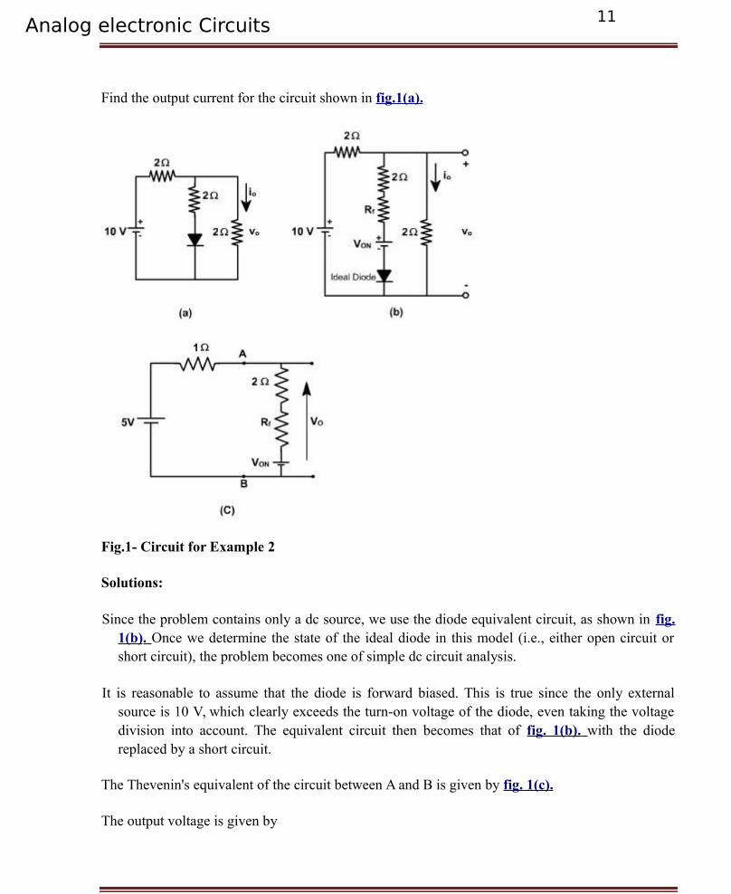
Find the output current for the circuit shown in fig.1(a).
Fig.1- Circuit for Example 2
Solutions:
Since the problem contains only a dc source, we use the diode equivalent circuit, as shown in fig.1(b) . Once we determine the state of the ideal diode in this model (i.e., either open circuit orshort circuit), the problem becomes one of simple dc circuit analysis.
It is reasonable to assume that the diode is forward biased. This is true since the only externalsource is 10 V, which clearly exceeds the turn-on voltage of the diode, even taking the voltagedivision into account. The equivalent circuit then becomes that of fig. 1(b). with the diodereplaced by a short circuit.
The Thevenin's equivalent of the circuit between A and B is given by fig. 1(c).
The output voltage is given by

Analog electronic Circuits 12
or,
If VON= 0.7V, and Rf= 0.2 W , then
Vo = 3.66V
Diode Operating Point
Example - 3
The circuit of fig. 2, has a source voltage of Vs = 1.1 + 0.1 sin 1000t. Find the current, iD. Assume that
nVT = 40 mV
VON = 0.7 V
Solution:
We use KVL for dc equation to yield
Vs= VON+ ID RL
Fig.2
This sets the dc operating point of the diode. We need to determine the dynamic resistance sowe can establish the resistance of the forward-biased junction for the ac signal.

Analog electronic Circuits 13
Assuming that the contact resistance is negligible Rf= rD Now we can replace the forward-biased diode with a 10 W resistor. Again using KVL, we have,
vs= Rf id + RL id
The diode current is given by
I = 4 + 0.91 sin 1000 t mA
Since iD is always positive, the diode is always forward-biased, and the solution is complete.
This sets the dc operating point of the diode. We need to determine the dynamic resistance sowe can establish the resistance of the forward-biased junction for the ac signal.
Assuming that the contact resistance is negligible Rf= rD Now we can replace the forward-biased diode with a 10 W resistor. Again using KVL, we have,
vs= Rf id + RL id
The diode current is given by
I = 4 + 0.91 sin 1000 t mA
Since iD is always positive, the diode is always forward-biased, and the solution is complete.
Diode Operating Point
Small Signal Operation of Real diode:
Consider the diode circuit shown in fig. 3 .
V = VD + Id RL VD = V-
IdRL
This equation involves two unknowns and cannot be solved. The straight line represented by the above equation is known as the load line. The load line passes through two points,

Analog electronic Circuits 14
I = 0, VD = V
and VD= 0, I = V / RL.
The slope of this line is equal to 1/ RL. The other equation in terms of these two variables VD& Id, is given by the static characteristic. The point of intersection of straight line and diode
characteristic gives the operating point as shown in fig. 4.
ohm.
The resulting input voltage is the sum of dc voltage and sinusoidal ac voltage. Therefore, asthe diode voltage varies, diode current also varies, sinusoidally. The intersection of loadline and diode characteristic for different input voltages gives the output voltage as shownin fig. 6.

Analog electronic Circuits 15
Fig. 6
In certain applications only ac equivalent circuit is required. Since only ac response of thecircuit is considered DC Source is not shown in the equivalent circuit of fig. 7. Theresistance rf represents the dynamic resistance or ac resistance of the diode. It is obtainedby taking the ratio of VD/ ID at operating point.
Dynamic Resistance rD = VD / ID
Let us consider a circuit shown in fig. 5 having dc voltage and sinusoidal ac voltage. Say

Analog electronic Circuits 16
V = 1V, RL=10
Fig. 7
Applications of Diode
Diode Approximation: (Large signal operations):
1. Ideal Diode:
When diode is forward biased, resistance offered is zero,When it is reverse biased resistance offered is infinity. It acts as a perfect switch.
The characteristic and the equivalent circuit of the diode is shown in fig. 1.
Fig. 1
2. Second Approximation:
When forward voltage is more than 0.7 V, for Si diode then it conducts and offers zero resistance. The drop across the diode is 0.7V.
When reverse biased it offers infinite resistance.

Analog electronic Circuits 17
The characteristic and the equivalent circuit is shown in fig. 2.
Fig. 2
3. 3rd Approximation:
• When forward voltage is more than 0.7 V, then the diode conducts and the voltage drop across the diode becomes 0.7 V and it offers resistance Rf (slope of the current)
VD= 0.7 + ID Rf.
The output characteristic and the equivalent circuit is shown in fig. 3.
Fig. 3
When reverse biased resistance offered is very high & not infinity, then the diode equivalent circuit is as shown in fig. 4.

Analog electronic Circuits 18
Fig. 4
Example - 1:
Calculate the voltage output of the circuit shown in fig. 5 for following inputs
(a) V1 = V2 = 0.
(b) V1 = V, V2 = 0.
(c) V 1 = V2 = V knew voltage = Vr
Forward resistance of each diode is Rf.
Solution:
(a). When both V1 and V2 are zero , then the diodes are unbiased. Therefore,
Vo = 0 V

Analog electronic Circuits 19
(b). When V1 = V and V2 = 0, then one upper diode is forward biased and lower diode is unbiased.
The resultant circuit using third approximation of diode will be as shown in fig. 6 .
Fig. 6 Fig. 7
Applying KVL, we get
(c) When both V1 and V2 are same as V, then both the diodes are forward biased and conduct. The resultant
circuit using third approximation of diode will be as shown in Fig. 7 .
Half wave Rectifier:
The single ? phase half wave rectifier is shown in fig. 8 .
Fig. 8 Fig. 9

Analog electronic Circuits 20
In positive half cycle, D is forward biased and conducts. Thus the output voltage is same as theinput voltage. In the negative half cycle, D is reverse biased, and therefore output voltage iszero. The output voltage waveform is shown in fig. 9.
The average output voltage of the rectifier is given by
The average output current is given by
When the diode is reverse biased, entire transformer voltage appears across the diode. Themaximum voltage across the diode is Vm. The diode must be capable to withstand this voltage.Therefore PIV half wave rating of diode should be equal to Vm in case of single-phase rectifiers.The average current rating must be greater than Iavg
Full Wave Rectifier:
A single ? phase full wave rectifier using center tap transformer is shown in fig. 10. It supplies current in both half cycles of the input voltage.
Fig. 10 Fig. 11
In the first half cycle D1 is forward biased and conducts. But D2 is reverse biased and does not
conduct. In the second half cycle D2 is forward biased, and conducts and D1 is reverse biased. Itis also called 2 ? pulse midpoint converter because it supplies current in both the half cycles.The output voltage waveform is shown in fig. 11 .
The average output voltage is given by

Analog electronic Circuits 21
and the average load current is given by
When D1 conducts, then full secondary voltage appears across D2, therefore PIV rating of the
diode should be 2 Vm.
Bridge Rectifier:
The single ? phase full wave bridge rectifier is shown in fig. 1. It is the most widely used rectifier.It also provides currents in both the half cycle of input supply.
Fig. 1 Fig. 2
In the positive half cycle, D1 & D4 are forward biased and D2 & D3 are reverse biased. In the
negative half cycle, D2 & D3 are forward biased, and D1 & D4 are reverse biased. The outputvoltage waveform is shown in fig. 2 and it is same as full wave rectifier but the advantage is thatPIV rating of diodes are V m and only single secondary transformer is required.
The main disadvantage is that it requires four diodes. When low dc voltage is required thensecondary voltage is low and diodes drop (1.4V) becomes significant. For low dc output, 2-pulse center tap rectifier is used because only one diode drop is there.
The ripple factor is the measure of the purity of dc output of a rectifier and is defined as

Analog electronic Circuits 22
Therefore,
Clippers:
Clipping circuits are used to select that portion of the input wave which lies above or below somereference level. Some of the clipper circuits are discussed here. The transfer characteristic (vo vsvi) and the output voltage waveform for a given input voltage are also discussed.
Clipper Circuit 1:
The circuit shown in fig. 3 , clips the input signal above a reference voltage (VR).
In this clipper circuit,
If vi < VR, diode is reversed biased and does not
conduct. Therefore, vo = vi
and, if vi > VR, diode is forward biased and thus, vo= VR.
The transfer characteristic of the clippers is shown in fig. 4. Fig. 3

Analog electronic Circuits 23
Fig. 4
Clipper Circuit 2:
The clipper circuit shown in fig. 5 clips the input signal below reference voltage VR.
In this clipper circuit,
If vi > VR, diode is reverse biased. vo = vi
and, If vi < VR, diode is forward biased. vo = VR
The transfer characteristic of the circuit is shown in fig. 6. Fig. 5
Fig. 6
Clipper Circuit 3: To clip the input signal between two
independent levels (VR1< VR2 ), the clipper circuit isshown in fig. 7.
The diodes D1 & D2 are assumed ideal diodes.
For this clipper circuit, when vi ≤ VR1, vo=VR1
and, vi ≥ VR2, vo= VR2
Fig. 7

Analog electronic Circuits 24
and, VR1 < vi < VR2 vo = vi
The transfer characteristic of the clipper is shown in fig. 8.
Fig. 8
Clippers:
Clipping circuits are used to select that portion of the input wave which lies above or below somereference level. Some of the clipper circuits are discussed here. The transfer characteristic (vo vsvi) and the output voltage waveform for a given input voltage are also discussed.
Clipper Circuit 1:
The circuit shown in fig. 3 , clips the input signal above a reference voltage (VR).
In this clipper circuit,
If vi < VR, diode is reversed biased and does not
conduct. Therefore, vo = vi
and, if vi > VR, diode is forward biased and thus, vo= VR.
The transfer characteristic of the clippers is shown in fig. 4. Fig. 3

Analog electronic Circuits 25
Fig. 4
Clipper Circuit 2:
The clipper circuit shown in fig. 5 clips the input signal below reference voltage VR.
In this clipper circuit,
If vi > VR, diode is reverse biased. vo = vi
and, If vi < VR, diode is forward biased. vo = VR
The transfer characteristic of the circuit is shown in fig. 6. Fig. 5
Fig. 6

Analog electronic Circuits 26
Clipper Circuit 3:
To clip the input signal between two independent levels (VR1< VR2 ), the clipper circuit is shown in fig. 7.
The diodes D1 & D2 are assumed ideal diodes.
For this clipper circuit, when vi ≤ VR1, vo=VR1
and, vi ≥ VR2, vo= VR2
and, VR1 < vi < VR2 vo = vi
Fig. 7The transfer characteristic of the clipper is shown in fig. 8.
Fig. 8
Example - 1:
Find the output voltage v out of the clipper circuit of fig. 7(a) assuming that the diodes are
a. ideal.
b. Von = 0.7 V. For both cases, assume RF is zero.

CAnalog electronic Circuits 27
Fig. 7(a) Fig. 7(b)
Solution:
(a). When vinis positive and vin < 3, then vout = vin
and when vin is positive and vin > 3, then
At vin = 8 V(peak), vout = 6.33 V.
When vinis negative and vin > - 4, then vout = vin
When vin is negative and vin < -4, then vout = -4V
The resulting output wave shape is shown in fig. 7(b) .
(b). When VON = 0.7 V, vin is positive and vin < 3.7 V, then vout = vin
When vin > 3.7 V, then
When vin = 8V, vout = 6.56 V.
When vin is negative and vin > -4.7 V, then vout = vin
When vin < - 4.7 V, then vout = - 4.7 V

Analog electronic Circuits 28
The resulting output wave form is shown in fig. 7(b).
Clamper Circuits:
Clamping is a process of introducing a dc level into a signal. For example, if the input voltageswings from -10 V and +10 V, a positive dc clamper, which introduces +10 V in the input willproduce the output that swings ideally from 0 V to +20 V. The complete waveform is lifted upby +10 V.
Negative Diode clamper:
A negative diode clamper is shown in fig. 8 , which introduces a negative dc voltage equal to peakvalue of input in the input signal.
Fig. 8 Fig. 9
Let the input signal swings form +10 V to -10 V.During first positive half cycle as V i rises from0 to 10 V, the diode conducts. Assuming an idealdiode, its voltage, which is also the output must
be zero during the time from 0 to t1. Thecapacitor charges during this period to 10 V,with the polarity shown.
At that Vi starts to drop which means the anode of D
is negative relative to cathode, ( VD = vi - vc ) thusreverse biasing the diode and preventing thecapacitor from discharging. Fig. 9 . Since thecapacitor is holding its charge it behaves as a
DC voltage source while the diode appears as an Fig. 10
open circuit, therefore the equivalent circuit

Analog electronic Circuits 29
becomes an input supply in series with -10 V dcvoltage as shown in fig. 10 , and the resultantoutput voltage is the sum of instantaneous inputvoltage and dc voltage (-10 V).
Positive Clamper:
The positive clamper circuit is shown in fig. 1 , which introduces positive dc voltage equal to thepeak of input signal. The operation of the circuit is same as of negative clamper.
Fig. 1 Fig. 2
Let the input signal swings form +10 V to -10 V. During first negative half cycle as Vi rises from 0to -10 V, the diode conducts. Assuming an ideal diode, its voltage, which is also the output must
be zero during the time from 0 to t1. The capacitor charges during this period to 10 V, with thepolarity shown.
After that Vi starts to drop which means the anode of D is negative relative to cathode, (VD= vi -
vC) thus reverse biasing the diode and preventing the capacitor from discharging. Fig. 2. Sincethe capacitor is holding its charge it behaves as a DC voltage source while the diode appears asan open circuit, therefore the equivalent circuit becomes an input supply in series with +10 V dcvoltage and the resultant output voltage is the sum of instantaneous input voltage and dc voltage(+10 V).
To clamp the input signal by a voltage other than peak value, a dc source is required. As shown infig. 3 , the dc source is reverse biasing the diode.
The input voltage swings from +10 V to -10 V. In the negative half cycle when the voltage exceed5V then D conduct. During input voltage variation from ?5 V to -10 V, the capacitor charges to

Analog electronic Circuits 30
5 V with the polarity shown in fig. 3 . After that D becomes reverse biased and open circuited.Then complete ac signal is shifted upward by 5 V. The output waveform is shown in fig. 4.
Fig. 3 Fig. 4
Voltage Doubler :
A voltage doubler circuit is shown in fig. 5 . The circuit produces a dc voltage, which is double thepeak input voltage.
Fig. 5 Fig. 6
At the peak of the negative half cycle D1 is forward based, and D2 is reverse based. This chargesC1 to the peak voltage Vp with the polarity shown. At the peak of the positive half cycle D1 isreverse biased and D2 is forward biased. Because the source and C1 are in series, C2 will changetoward 2Vp. e.g. Capacitor voltage increases continuously and finally becomes 20V. The voltagewaveform is shown in fig. 6 .

Analog electronic Circuits 31
To understand the circuit operation, let the input voltage varies from -10 V to +10 V. The differentstages of circuit from 0 to t10 are shown in fig. 7(a) .
Fig. 7(a)
During 0 to t1, the input voltage is negative, D1 is forward biased the capacitor is charged to ?10 V
with the polarity as shown in fig. 7b .
Fig. 7(b)
During t1 to t2, D2 becomes forward biased and conducts and at t2, when Vi is 10V total voltagechange is 20V. If C1 = C2 = C, both the capacitor voltages charge to +10 V i.e. C1 voltagebecomes 0 and C2 charges to +10V.

Analog electronic Circuits 32
Fig. 7(c)
From t2 to t3 there is no conduction as both D1 and D2 are reverse biased. During t3 to t4 D1 is
forward biased and conducts. C1 again charges to +10V
Fig. 7(d)
During t4 to t5 both D1 and D2 are reverse biased and do not conduct. During t5 to t6 D2 is forward
biased and conducts. The capacitor C2 voltage becomes +15 V and C1 voltage becomes +5 V.
Fig. 7(e)
Analog electronic Circuits 33
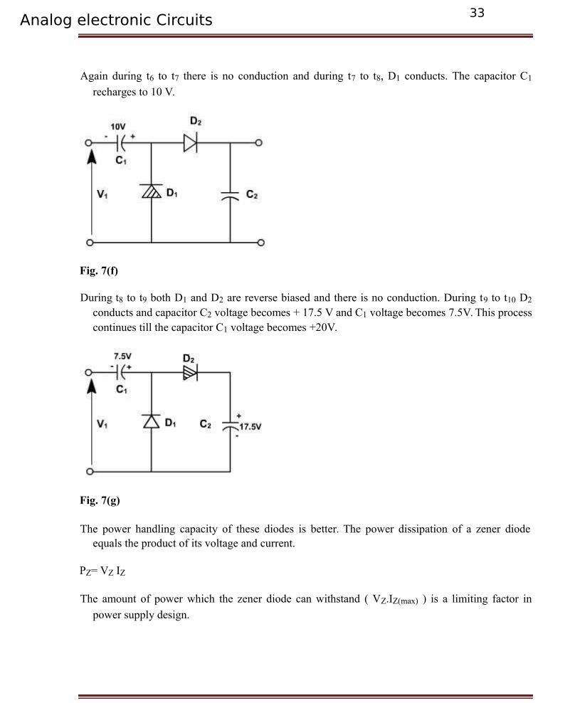
Again during t6 to t7 there is no conduction and during t7 to t8, D1 conducts. The capacitor C1
recharges to 10 V.
Fig. 7(f)
During t8 to t9 both D1 and D2 are reverse biased and there is no conduction. During t9 to t10 D2
conducts and capacitor C2 voltage becomes + 17.5 V and C1 voltage becomes 7.5V. This processcontinues till the capacitor C1 voltage becomes +20V.
Fig. 7(g)
The power handling capacity of these diodes is better. The power dissipation of a zener diodeequals the product of its voltage and current.
PZ= VZ IZ
The amount of power which the zener diode can withstand ( VZ.IZ(max) ) is a limiting factor in
power supply design.
Analog electronic Circuits 34
Transistor biasing
To Understand :
• Concept of Operating point and stability
• Analyzing Various biasing circuits and their comparison with respect to stability
BJT – A Review
• Invented in 1948 by Bardeen, Brattain and Shockley
• Contains three adjoining, alternately doped semiconductor regions: Emitter (E), Base (B), and Collector (C)
• The middle region, base, is very thin
• Emitter is heavily doped compared to collector. So, emitter and collector are not interchangeable.
Three operating regions
• Linear – region operation:
– Base – emitter junction forward biased
– Base – collector junction reverse biased
• Cutoff – region operation:
– Base – emitter junction reverse biased
– Base – collector junction reverse biased
• Saturation – region operation:
– Base – emitter junction forward biased
– Base – collector junction forward biased

Analog electronic Circuits 35
Three operating regions of BJT
• Cut off: VCE = VCC, IC ≅ 0
• Active or linear : VCE ≅ VCC/2 , IC ≅ IC max/2
• Saturation: VCE ≅ 0 , IC ≅ IC max
Q-Point
• The intersection of the dc bias value of IB with the dc load line determines the Q- point.
• It is desirable to have the Q-point centered on the load line. Why?
• When a circuit is designed to have a centered Q-point, the amplifier is said to be midpoint biased.
• Midpoint biasing allows optimum ac operation of the amplifier.
Introduction - Biasing
The analysis or design of a transistor amplifier requires knowledge of both thedc and ac response of the system.In fact, the amplifier increases the strengthof a weak signal by transferring the energy from the applied DC source to theweak input ac signal
• The analysis or design of any electronic amplifier therefore has two components:
• The dc portion and
• The ac portion
Analog electronic Circuits 36
During the design stage, the choice of parameters for the required dc levels will affect the ac response.
What is biasing circuit?
• Once the desired dc current and voltage levels have been identified, a network must be constructed that will establish the desired values of IB, IC and VCE, Such a network is known as biasing circuit. A biasing network has to preferably make
use of one power supply to bias both the junctions of the transistor.
Purpose of the DC biasing circuit
• To turn the device“ON”
• To place it in operation in the region of its characteristic where the device
operates most linearly, i.e. to set up the initial dc values of IB, IC, and VCE
Important basic relationship
• VBE = 0.7V
• IE = (β + 1) IB ≅ IC
• IC = β IB

Analog electronic Circuits 37
Collector-to-base bias
Collector-to-base bias
This configuration employs negative feedback to prevent thermal runaway and stabilize theoperating point. In this form of biasing, the base resistor RB is connected to the collector instead ofconnecting it to the DC source VCC. So any thermal runaway will induce a voltage drop across theRC resistor that will throttle the transistor's base current.
From Kirchhoff's voltage law, the voltage across the base resistor Rb is
By the Ebers–Moll model, Ic = βIb, and so
From Ohm's law, the base current , and so
Hence, the base current Ib is
If Vbe is held constant and temperature increases, then the

Analog electronic Circuits 38
collector current Ic increases. However, a larger Ic causes the voltage drop across resistor Rc to
increase, which in turn reduces the voltage across the base resistor Rb. A lower base-resistor
voltage drop reduces the base current Ib, which results in less collector current Ic. Because anincrease in collector current with temperature is opposed, the operating point is kept stable.
Merits:
Circuit stabilizes the operating point against variations in temperature and β (ie. replacement of transistor)
Demerits:
In this circuit, to keep Ic independent of β, the following condition must be met:
which is the case when
As β-value is fixed (and generally unknown) for a given transistor, this relation can be satisfied either by keeping Rc fairly large or making Rb very low.
If Rc is large, a high Vcc is necessary, which increases cost as well as precautions necessary while handling.
If Rb is low, the reverse bias of the collector–base region is small, which limits the range of collector voltage swing that leaves the transistor in active mode.
The resistor Rb causes an AC feedback, reducing the voltage gain of the amplifier. This
undesirable effect is a trade-off for greater Q-point stability.
Usage: The feedback also decreases the input impedance of the amplifier as seen from the base,which can be advantageous. Due to the gain reduction from feedback, this biasing form is usedonly when the trade-off for stability is warranted

39
Analog electronic Circuits
Biasing circuits:
• Fixed – bias circuit
• Emitter bias
• Voltage divider bias
• DC bias with voltage feedback
• Miscellaneous bias
• The simplest transistor dc bias configuration.
• For dc analysis, open all the capacitance.
DC Analysis
• Applying KVL to the input loop:
VCC = IBRB + VBE
• From the above equation, deriving for IB, we get,
IB = [VCC – VBE] / RB
• The selection of RB sets the level of base current for the operating point.
• Applying KVL for the output loop:
VCC = ICRC + VCE
RC

40
S( ICO) = β + 1
This indicates poor stability.
Voltage divider configuration
S( ICO) = ( β + 1) [ 1 + RB / RE] / [( β +
1) + RB / RE] Here, replace RB with Rth
S( ICO) = ( β + 1) [ 1 + Rth / RE] / [( β + 1) + Rth / RE]
Thus, voltage divider bias configuration is quite stable when the ratio R / R is as small
Physical impact
In a fixed bias circuit, IC increases due to increase in IC0. [IC = βIB + (β+1) IC0]
IB is fixed by VCC and RB. Thus level of IC would continue to rise with temperature –
a very unstable situation.
In emitter bias circuit, as IC increases, IE increases, VE increases. Increase in VE reduces
IB. IB = [VCC – VBE – VE] / RB. A drop in IB reduces IC.Thus, this configuration is
such that there is a reaction to an increase in IC that will tend to oppose the change in bias
conditions.
In the DC bias with voltage feedback, as IC increases, voltage across RC increases, thus
reducing IB and causing IC to reduce.
The most stable configuration is the voltage – divider network. If the condition βRE
>>10R2, the voltage VB will remain fairly constant for changing levels of IC. VBE =
VB – VE, as IC increases, VE increases, since VB is constant, VBE drops making IB to
fall, which will try to offset the increases level of IC.

41
S(VBE)
S(VBE) = ∆IC / ∆VBE
For an emitter bias circuit, S(VBE) = - β / [ RB + (β + 1)RE]
If RE =0 in the above equation, we get S(VBE) for a fixed bias circuit as, S(VBE) = - β / RB.
For an emitter bias,
S(VBE) = - β / [ RB + (β + 1)RE] can be
rewritten as, S(VBE) = - (β/RE )/
[RB/RE + (β + 1)]
If (β + 1)>> RB/RE, then
The larger the RE, lower the S(VBE) and more stable is
the system. Total effect of all the three parameters onIC can be written as,
Forward active mode of operation
The forward active mode is obtained by forward-biasing the base-emitter junction. In addition
we eliminate the base-collector junction current by setting VBC = 0. The minority-carrier distribution in the quasi-neutral regions of the bipolar transistor, as shown in Figure, is usedto analyze this situation in more detail.
42
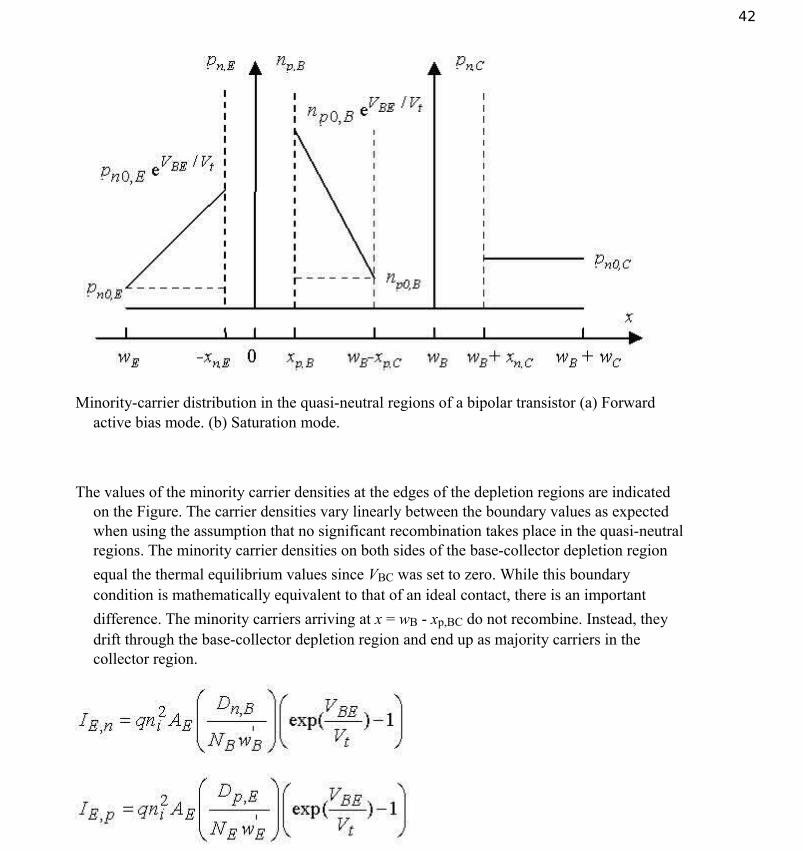
Minority-carrier distribution in the quasi-neutral regions of a bipolar transistor (a) Forwardactive bias mode. (b) Saturation mode.
The values of the minority carrier densities at the edges of the depletion regions are indicated on the Figure. The carrier densities vary linearly between the boundary values as expected when using the assumption that no significant recombination takes place in the quasi-neutralregions. The minority carrier densities on both sides of the base-collector depletion region
equal the thermal equilibrium values since VBC was set to zero. While this boundary condition is mathematically equivalent to that of an ideal contact, there is an important
difference. The minority carriers arriving at x = wB - xp,BC do not recombine. Instead, they drift through the base-collector depletion region and end up as majority carriers in the collector region.

43
And the emitter current due to electrons, IE,n, simplifies to:
It is convenient to rewrite the emitter current due to electrons, IE,n, as a function of the total
excess minority charge in the base, Qn,B. This charge is proportional to the triangular area in the quasi-neutral base as shown in Figure and is calculated from
where tr is the average time the minority carriers spend in the base layer, i.e. the transit time.The emitter current therefore equals the excess minority carrier charge present in the baseregion, divided by the time this charge spends in the base. This and other similar relationswill be used to construct the charge control model of the bipolar junction transistor A combination of equations yields the transit time as a function of the quasi-neutral layer
width, wB', and the electron diffusion constant in the base, Dn,B.
We now turn our attention to the recombination current in the quasi-neutral base and obtain itfrom the continuity equation
By applying it to the quasi-neutral base region and assuming steady state conditions:

44
which in turn can be written as a function of the excess minority carrier charge, Qn,B, using
equation
It is typically the emitter efficiency, which limits the current gain in transistors made of siliconor germanium. The long minority-carrier lifetime and the long diffusion lengths in those materials justify the exclusion of recombination in the base or the depletion layer. The resulting current gain, under such conditions, is:
From this equation, we conclude that the current gain can be larger than one if the emitterdoping is much larger than the base doping. A typical current gain for a silicon bipolartransistor is 50 - 150.
This expression is only valid if the base transport factor is very close to one, since it was derived using the “short-diode” carrier distribution. This base transport factor can also be
expressed in function of the diffusion length in the base:

45
Uni-junction transistor
The UJT as the name implies, is characterized by a single pn junction. It exhibits negativeresistance characteristic that makes it useful in oscillator circuits.
The symbol for UJT is shown in fig. 1 . The UJT is having three terminals base1 (B1), base2(B2) and emitter (E). The UJT is made up of an N-type silicon bar which acts as the base asshown in fig. 2 . It is very lightly doped. A P-type impurity is introduced into the base,producing a single PN junction called emitter. The PN junction exhibits the properties of aconventional diode.
Fig. 1Fig .2
A complementary UJT is formed by a P-type base and N-type emitter. Except for the polarity ofvoltage and current the characteristic is similar to those of a conventional UJT.
A simplified equivalent circuit for the UJT is shown in fig. 3 . VBB is a source of biasing voltageconnected between B2 and B1. When the emitter is open, the total resistance from B2 to B1is simply the resistance of the silicon bar, this is known as the inter base resistance RBB.
Since the N-channel is lightly doped, therefore RBB is relatively high, typically 5 to 10K
ohm. RB2 is the resistance between B2 and point ?a', while RB1 is the resistance from point ?
a' to B1, therefore the interbase resistance RBB is
RBB = RB1 + RB2

46
Fig. 3
The diode accounts for the rectifying properties of the PN junction. VD is the diode's threshold
voltage. With the emitter open, IE = 0, and I1 = I 2 . The interbase current is given by
I1 = I2 = VBB / R BB .
Part of VBB is dropped across RB2 while the rest of voltage is dropped across RB1. The voltage
across RB1 is
Va = VBB * (RB1 ) / (RB1 + RB2 )
The ratio RB1 / (RB1 + RB2 ) is called intrinsic standoff ratio
= RB1 / (RB1 + RB2 ) i.e. Va =VBB .
The ratio is a property of UJT and it is always less than one and usually between 0.4 and 0.85. As long as IB = 0, the circuit of behaves as a voltage divider.
Assume now that vE is gradually increased from zero using an emitter supply VEE . The diode
remains reverse biased till vE voltage is less than VBB and no emitter current flows exceptleakage current. The emitter diode will be reversed biased.
When vE = VD + VBB, then appreciable emitter current begins to flow where VD is the diode'sthreshold voltage. The value of vE that causes, the diode to start conducting is called thepeak point voltage and the current is called peak point current IP.
VP = VD + VBB.

47
The graph of fig. 4 shows the relationship between the emitter voltage and current. vE is plotted on
the vertical axis and IE is plotted on the horizontal axis. The region from vE = 0 to vE = VP is
called cut off region because no emitter current flows (except for leakage). Once v E exceeds the
peak point voltage, IE increases, but v E decreases. up to certain point called valley point (VV
and IV). This is called negative resistance region. Beyond this, IE increases with vE this is thesaturation region, which exhibits a positive resistance characteristic.
The physical process responsible for the negative resistance characteristic is called
conductivity modulation. When the vE exceeds VP voltage, holes from P emitter are injectedinto N base. Since the P region is heavily doped compared with the N-region, holes are injected to the lower half of the UJT
Fig. 4
The lightly doped N region gives these holes a long lifetime. These holes move towards B1 tocomplete their path by re-entering at the negative terminal of VEE. The large holes create aconducting path between the emitter and the lower base. These increased charge carriers

48
represent a decrease in resistance RB1, therefore can be considered as variable resistance. It
decreases up to 50 ohm.
Since is a function of RB1 it follows that the reduction of RB1 causes a corresponding reductionin intrinsic standoff ratio. Thus as IE increases, RB1 decreases, decreases, and Va decreases.The decrease in V a causes more emitter current to flow which causes further reduction inRB1, , and Va. This process is regenerative and therefore Va as well as vE quickly dropswhile IE increases. Although RB decreases in value, but it is always positive resistance. It isonly the dynamic resistance between VV and VP. At point B, the entire base1 region willsaturate with carriers and resistance RB1 will not decrease any more. A further increase in Iewill be followed by a voltage rise.
The diode threshold voltage decreases with temperature and RBB resistance increases with
temperature because Si has positive temperature coefficient.
UJT Relaxation Oscillator:
The characteristic of UJT was discussed in previous lecture. It is having negative resistanceregion. The negative dynamic resistance region of UJT can be used to realize an oscillator.
The circuit of UJT relaxation oscillator is shown in fig. 1 . It includes two resistors R1 and R2 fortaking two outputs R2 may be a few hundred ohms and R1 should be less than 50 ohms. The dcsource VCC supplies the necessary bias. The interbase voltage VBB is the difference betweenVCC and the voltage drops across R1 and R2. Usually RBB is much larger than R1 and R2 so thatVBB approximately equal to V. Note, RB1 and RB2 are inter-resistance of UJT while R1 and R2 isthe actual resistor. RB1 is in series with R1 and RB2 is in series with R2 .

49
Fig. 1
As soon as power is applied to the circuit capacitor begins to charge toward V. The voltageacross C, which is also VE , rises exponentially with a time constant
= R C
As long as VE < VP, IE = 0. the diode remains reverse biased as long as VE < VP . When thecapacitor charges up to VP , the diode conducts and RB1 decreases and capacitor startsdischarging. The reduction in R B1 causes capacitor C voltage to drop very quickly to thevalley voltage VV because of the fast time constant due to the low value of RB1 and R1. Assoon as VE drops below Va + VD the diode is no longer forward biased and it stopsconduction. It now reverts to the previous state and C begins to charge once more towardVCC .
The emitter voltage is shown in fig. 2 , VE rises exponentially toward VCC but drops to a very
low value after it reaches VP. The time for the VE to drop from VP to VV is relatively smalland usually neglected. The period T can therefore be approximated as follows:

50
Fig. 2

51
There are two additional outputs possible for the UJT oscillation one of these is the voltagedeveloped at B1 due to capacitor discharge while the other is voltage developed at B2 asshown in fig. 3 .
When UJT fires (at t = T) Va drops, causing a
corresponding voltage drop at B2. The duration ofoutputs at B1 and B2 are determined by C dischargetime.
If R1 is very small, C discharges very quickly and very
narrow pulse is produced at the output. If R1 = 0,obviously no pulses appear at B1.
If R2 = 0, no pulse can be generated at B2. If R1 is toolarge, its positive resistance may swamp the negativeresistance and prevent the UJT form switching backafter it has fired.
R2, in addition to providing a source of pulse at B2, isuseful for temperature stabilization of the UJT's peakpoint voltage .
VP = VD + VBB.
Asthe temperature increases, Vp decreases. The
temperature coefficient of RBB is positive. Rs isessentially independent of temperature. It is thereforepossible to select R2 so that VBB increases with
temperature by the same amount as VD decreases.
This provides a constant VP and, in turn, frequencyof oscillation.
Selection of R and C:
Figure 31.3
In the circuit, R is required to pass only the capacitor charging current. At the instant when VP
is reached; R must supply the peak current. It is therefore, necessary, that the current throughR should be slightly greater than the peak point.

52
Once the UJT fires, VE drops to the valley voltage VV . IE should not be allowed to increases
beyond the valley point IV, otherwise the UJT is taken into saturation region and does notswitch back, R therefore must be selected large enough to ensure that
As long as R is chosen between these extremes, reliable operation results.
Frequency Response of Amplifier
Frequency curve of an RC coupled amplifier:
A practical amplifier circuit is meant to raise the voltage level of the input signal. This signalmay be obtained from anywhere e.g. radio or TV receiver circuit. Such a signal is not of asingle frequency. But it consists of a band of frequencies, e.g. from 20 Hz to 20 KHz. If theloudspeakers are to reproduce the sound faithfully, the amplifier used must amplify all thefrequency components of signal by same amount. If it does not do so, the output of theloudspeaker will not be the exact replica of the original sound. When this happen then itmeans distortion has been introduced by the amplifier. Consider an RC coupled amplifiercircuit shown in fig. 1 .

53
Fig. 1 Fig. 2
Fig. 2 , shows frequency response curve of a RC coupled amplifier. The curve is usually plottedon a semilog graph paper with frequency range on logarithmic scale so that large frequencyrange can be accommodated. The gain is constant for a limited band of frequencies. This
range is called mid-frequency band and gain is called mid band gain. AVM. On both sides ofthe mid frequency range, the gain decreases. For very low and very high frequencies thegain is almost zero.
In mid band frequency range, the coupling capacitors and bypass capacitors are as good asshort circuits. But when the frequency is low. These capacitors can no longer be replaced bythe short circuit approximation.
First consider coupling capacitor. The ac equivalent is shown in fig. 3 , assuming capacitors areoffering some impedance. In mid-frequency band, the capacitors are ac shorted so the inputvoltage appears directly across r'e but at low frequency the XC is significant and somevoltage drops across XC. The input vin at the base decreases. Thus decreasing output voltage.The lower the frequency the more will be XC and lesser will be the output voltage.

54
Fig. 3
Similarly at low frequency, output capacitor reactance also increases. The voltage across RL
also reduces because some voltage drop takes place across XC. Thus output voltage reduces.
The XC reactance not only reduces the gain but also change the phase between input and
output. It would not be exactly 180o but decided by the reactance. At zero frequency, thecapacitors are open circuited therefore output voltage reduces to zero.
The other component due to which gain decreases at low frequencies is the bypass capacitor.The function of this capacitor is to bypass ac and blocks dc The impedence of this capacitorin mid frequency band is very low as compared to RE so it behaves like ac short but as thefrequency decrease the XCE becomes more and no longer behaves like ac short. Now theemitter is not ac grounded. The ac emitter current i.e. divides into two parts i1 and i2, as

55
shown in fig. 4 . A current i1 passes through RE and rest of the current passes through C. Dueto ac current i1 in RE, an ac voltage is developed i1 * RE. With the polarity marked at aninstant. Thus the effective VL voltage is given by
Vbe = Vs ? RE.
Thus the effective voltage input is reduced. The output also reduces. The lower the frequency, the lesser will be the gain. This reduction in gain is due to negative feedback.
As the frequency of the input signal increases, again the gain of the amplifier reduces. Firstlythe of the transistor decreases at higher frequency. Thus reducing the voltage gain of theamplifier at higher frequencies as shown in fig. 5 .
The other factor responsible for the reduction in gain at higher frequencies is the presence ofvarious capacitors as shown in fig. 6 . They are not physically connected but inherentlypresent with the device.
Fig. 5
The capacitor Cbc between the base and the collector connects the output with the input.Because of this, negative feedback takes place in the circuit and the gain decreases. This
feedback effect is more, when Cbc provides a path for higher frequency ac currents
The capacitance Cbe offers a low input impedance at higher frequency thus reduces the
effective input signal and so the gain falls. Similarly, Cce provides a shunting effect at highfrequencies in the output side and reduces gain of the amplifier.
Besides these junction capacitances there are wiring capacitance CW1 and CW2. These reactance are
very small but at high frequencies they become 5 to 20 p.f. For a multistage amplifier,

56
the effect of the capacitances Cce,CW1 and CW2 can be represented by single shunt
capacitance.
CS = CW1 + CW2 +Cce.
At higher frequency, the capacitor CS offers low input impedance and thus reduces the output.
Fig. 6
Bandwidth of an amplifier:
The gain is constant over a frequency range. The frequencies at which the gain reduces to70.7% of the maximum gain are known as cut off frequencies, upper cut off and lower cutoff frequency. fig. 7 , shows these two frequences. The difference of these two frequencies iscalled Band width (BW) of an amplifier.
BW = f2 ? f1.

57
Fig. 7
At f1 and f2, the voltage gain becomes 0.707 Am(1 / 2). The output voltage reduces to 1 / 2 of maximum output voltage. Since the power is proportional to voltage square, the output powerat these frequencies becomes half of maximum power. The gain on dB scale is given by
20 log10(V2 / V1) = 10 log 10 (V2 / V1)2 = 3 dB.
20 log10(V2 / V1) = 20 log10(0.707) =10 log10 (1 / 2)2 = 10 log10(1 / 2) = -3 dB.
If the difference in gain is more than 3 dB, then it can be detected by human. If it is less than 3 dB it cannot be detected.
Direct Coupling:
For applications, where the signal frequency is below 10 Hz, coupling and bypass capacitorscannot be used. At low frequencies, these capacitors can no longer be treated as ac shortcircuits, since they offer very high impedance. If these capacitors are used then their valueshave to be extremely large e.g. to bypass a 100 ohm emitter resistor at 10 Hz, we need acapacitor of approximately 1600 F. The lower the frequency the worse the problem becomes.
To avoid this, direct coupling is used. This means designing the stages without coupling andbypass capacitors, so that the direct current is coupled as well as alternating current. As aresult, there is no lower frequency limit. The amplifier enlarges the signal no matter havelow frequency including dc or zero frequency.
58
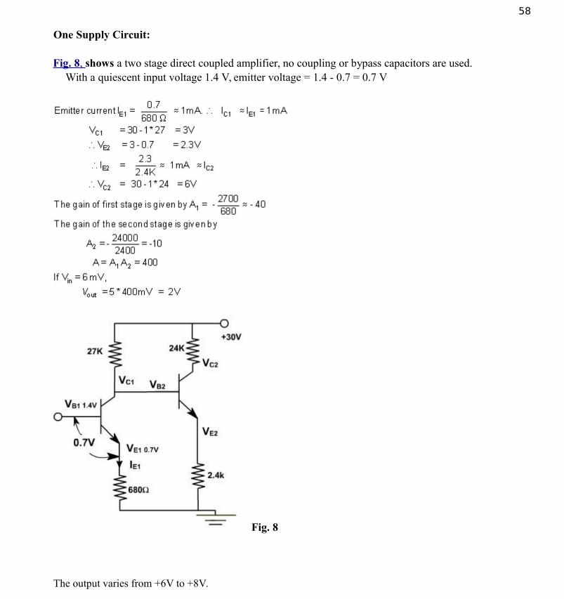
One Supply Circuit:
Fig. 8 , shows a two stage direct coupled amplifier, no coupling or bypass capacitors are used. With a quiescent input voltage 1.4 V, emitter voltage = 1.4 - 0.7 = 0.7 V
Fig. 8
The output varies from +6V to +8V.

59
The main disadvantage is variation in transistor characteristic with variation in temperature.
This causes IC and VC to change. Because of the direct coupling the voltage changes arecoupled from one stage to next stage, appearing at the final output as an amplified voltage.The unwanted change is called drift.
Grounded Reference Input
For the above amplifier, we need a quiescent voltage of 1.4V. In most applications, it isnecessary to have grounded reference input one where the quiescent input voltage is 0 V, asshown in fig. 9 .
Fig. 9
The quiescent V CE of the first transistor is only 0.7V and the quiescent of the second transistor
is only 1.4V. Both the transistors are operating in active region because VCE(sat) is only 0.1volt. The input is only in mV, which means that these transistors continue to operate in theactive region when a small signal is present.

60
h-Parameters
Small signal low frequency transistor Models:
All the transistor amplifiers are two port networks having two voltages and two currents. Thepositive directions of voltages and currents are shown in fig. 1 .
Fig. 1
Out of four quantities two are independent and two are dependent. If the input current i1 andoutput voltage v2 are taken independent then other two quantities i2 and v1 can be expressedin terms of i1 and V2.
The equations can be written as
where h11, h12, h21 and h22 are called h-parameters.
= hi = input impedance with output short circuit to ac.

61
=hr = fraction of output voltage at input with input open circuited or reverse voltage gain with
input open circuited to ac (dimensions).
= hf = negative of current gain with output short circuited to ac.
The current entering the load is negative of I2. This is also known as forward short circuit
current gain.
= ho = output admittance with input open circuited to ac.
If these parameters are specified for a particular configuration, then suffixes e,b or c are also included, e.g. hfe ,h ib are h parameters of common emitter and common collector amplifiers
Using two equations the generalized model of the amplifier can be drawn as shown in fig. 2 .
Fig. 2
The hybrid model for a transistor amplifier can be derived as follow:

62
Let us consider CE configuration as show in fig. 3 . The variables, iB, iC ,vC, and vB representtotal instantaneous currents and voltages iB and vC can be taken as independent variablesand vB, IC as dependent variables.
Fig. 3
vB = f1 (iB ,vC )
IC = f2 ( iB , vC ).
Using Taylor 's series expression, and neglecting higher order terms we obtain.
The partial derivatives are taken keeping the collector voltage or base current constant. The
vB, vC, iB, iC represent the small signal (incremental) base and collector current andvoltage and can be represented as vb ,ib ,vC ,iC.

63
The model for CE configuration is shown in fig. 4 .
Fig. 4
Determination of h - parameters:
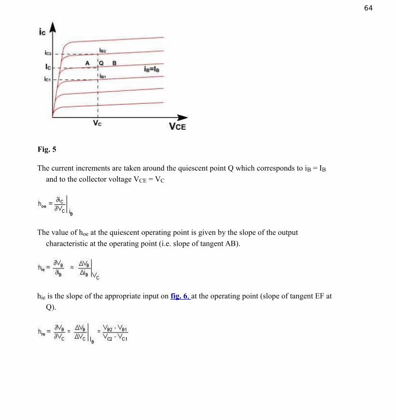
To determine the four h-parameters of transister amplifier, input and output characteristic areused. Input characteristic depicts the relationship between input voltage and input currentwith output voltage as parameter. The output characteristic depicts the relationship betweenoutput voltage and output current with input current as parameter. Fig. 5 , shows the outputcharacterisitcs of CE amplifier.
64
Fig. 5
The current increments are taken around the quiescent point Q which corresponds to iB = IB
and to the collector voltage VCE = VC
The value of hoe at the quiescent operating point is given by the slope of the output
characteristic at the operating point (i.e. slope of tangent AB).
hie is the slope of the appropriate input on fig. 6 , at the operating point (slope of tangent EF at
Q).

65
Fig. 6
A vertical line on the input characteristic represents constant base current. The parameter hre can be obtained from the ratio (VB2? V B1 ) and (VC2? V C1 ) for at Q.
Typical CE h-parametersof transistor 2N1573 are given below:
hie = 1000 ohm.
hre = 2.5 * 10 ?4
hfe = 50hoe = 25 A / V
Analysis of a transistor amplifier using h-parameters:
To form a transistor amplifier it is only necessary to connect an external load and signal source as indicated in fig. 1 and to bias the transistor properly.
Fig. 1

66
Consider the two-port network of CE amplifier. RS is the source resistance and ZL is the loadimpedence h-parameters are assumed to be constant over the operating range. The acequivalent circuit is shown in fig. 2 . (Phasor notations are used assuming sinusoidal voltageinput). The quantities of interest are the current gain, input impedence, voltage gain, andoutput impedence.
Fig. 2
Current gain:
For the transistor amplifier stage, Ai is defined as the ratio of output to input currents.
Input Impedence:
The impedence looking into the amplifier input terminals ( 1,1' ) is the input impedence Zi

67
Voltage gain:
The ratio of output voltage to input voltage gives the gain of the transistors.
Output Admittance:
It is defined as

68
Av is the voltage gain for an ideal voltage source (Rv = 0).
Consider input source to be a current source IS in parallel with a resistance RS as shown in fig.
3 .
Fig. 3
In this case, overall current gain AIS is defined as

69
To analyze multistage amplifier the h-parameters of the transistor used are obtained frommanufacture data sheet. The manufacture data sheet usually provides h-parameter in CEconfiguration. These parameters may be converted into CC and CB values. For example fig.
4 hrc in terms of CE parameter can be obtained as follows.
Fig. 4
For CE transistor configuaration
Vbe = hie Ib + hre Vce
Ic = h fe Ib + hoe Vce
The circuit can be redrawn like CC transistor configuration as shown in fig. 5 .
Vbc = hie Ib + hrc Vec
Ic = hfe Ib + hoe Vec
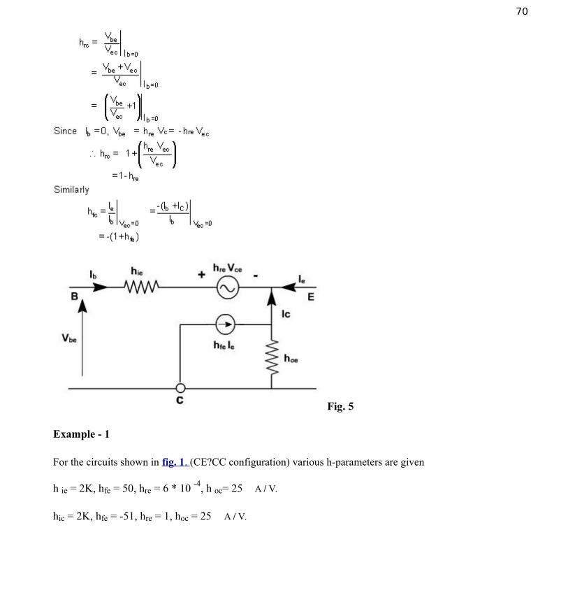
70
Fig. 5
Example - 1
For the circuits shown in fig. 1 . (CE?CC configuration) various h-parameters are given
h ie = 2K, hfe = 50, hre = 6 * 10 -4, h oc= 25 A / V.
hic = 2K, hfe = -51, hre = 1, hoc = 25 A / V.

71
Fig. 1
The small signal model of the transistor amplifier is shown in fig. 2.
Fig. 2
In the circuit, the collector resistance of first stage is shunted by the input impedence of laststage. Therefore the analysis is started with last stage. It is convenient; to first computecurrent gain, input impedence and voltage gain. Then output impedence is calculatedstarting from first stage and moving towards end.
72

The effective source resistance R'S2 for the second
stage is R01 || RC1 . Thus RS2 = R'01 = 4.65K

73
Overall current gain of the amplifier is Ai and is given by
The equivalent circuit of the amplifier is shown in fig. 3 . From the circuit it is clear that the current ic1 is divided into two parts.
Therefore,
and
Overall voltage gain of the amplifier is given by

74
Simplified common emitter hybrid model:
In most practical cases it is appropriate to obtain approximate values of A V , A i etc rather thancalculating exact values. How the circuit can be modified without greatly reducing theaccuracy. Fig. 4 shows the CE amplifier equivalent circuit in terms of h-parameters Since 1
/ hoe in parallel with RL is approximately equal to RL if 1 / hoe >> RL then hoe may be neglected. Under these conditions.
Ic = hfe IB .
hre vc = hre Ic RL = hre hfe Ib RL .
Fig. 4
75
Since h fe.h re 0.01, this voltage may be neglected in comparison with h ic Ib drop across h ieprovided RL is not very large. If load resistance RL is small than hoe and hre can beneglected.
Output impedence seems to be infinite. When Vs = 0, and an external voltage is applied at the
output we fined Ib = 0, I C = 0. True value depends upon RS and lies between 40 K and 80K.
On the same lines, the calculations for CC and CB can be done.
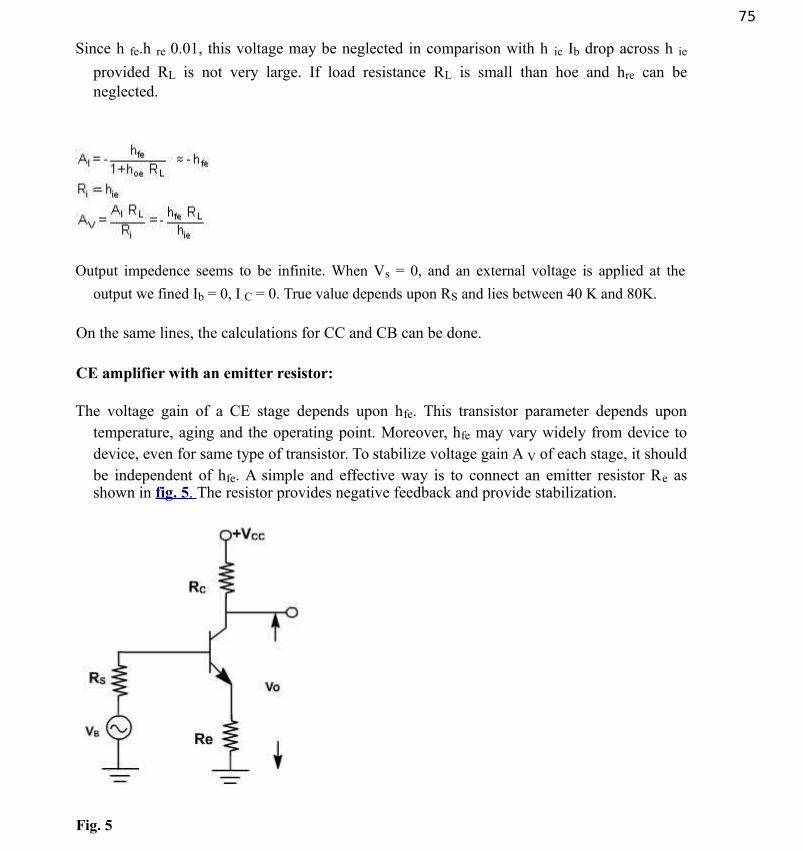
CE amplifier with an emitter resistor:
The voltage gain of a CE stage depends upon hfe. This transistor parameter depends upontemperature, aging and the operating point. Moreover, hfe may vary widely from device todevice, even for same type of transistor. To stabilize voltage gain A V of each stage, it shouldbe independent of hfe. A simple and effective way is to connect an emitter resistor Re asshown in fig. 5 . The resistor provides negative feedback and provide stabilization.
Fig. 5
76
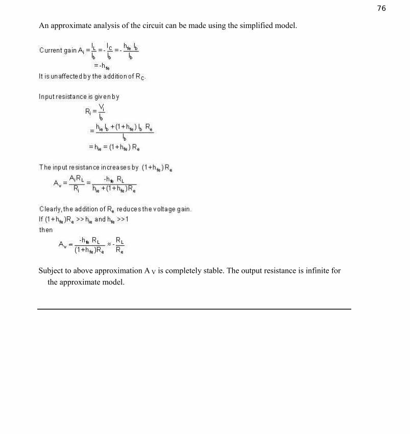
An approximate analysis of the circuit can be made using the simplified model.
Subject to above approximation A V is completely stable. The output resistance is infinite for
the approximate model.

77
Module-3
General Amplifiers
Darlington Amplifier:
It consists of two emitter followers in cascaded mode as shown in fig. 1 . The overall gain isclose to unity. The main advantage of Darlington amplifier is very large increase in inputimpedence and an equal decrease in output impedance .
Fig. 1
DC Analysis:
The first transistor has one VBE drop and second transistor has second VBE drop. The voltage
divider produces VTH to the input base. The dc emitter current of the second stage is
IE2 = (VTH ? 2 vBE ) / (RE )
The dc emitter current of the first stage that is the base current of second stage is given by
IE1 IE2 / 2
If r'e(2) is neglected then input impedance of second stage is

78
Zin (2) = 2 RE
This is the impedance seen by the first transistor. If r'e(1) is also neglected then the input
impedance of 1 becomes.
Zin (1) = 1 2 RE
which is extremely high because of the products of two betas, so the approximate input impedance of Darlington amplifier is
Zin = R1 || R2
Output impedance:
The Thevenin impedance at the input is given by
RTH = RS || R1 || R2
Similar to single stage common collector amplifier, the output impedance of the two stages zout(1) and zout(2) are given by.
Therefore, t he output impedance of the amplifier is very small.
which is extremely high because of the products of two betas, so the approximate input impedance of Darlington amplifier is
Zin = R1 || R2
Output impedance:
The Thevenin impedance at the input is given by

79
RTH = RS || R1 || R2
Similar to single stage common collector amplifier, the output impedance of the two stages zout(1) and zout(2) are given by.
Therefore, t he output impedance of the amplifier is very small.
which is extremely high because of the products of two betas, so the approximate input impedance of Darlington amplifier is
Zin = R1 || R2
Output impedance:
The Thevenin impedance at the input is given by
RTH = RS || R1 || R2
Similar to single stage common collector amplifier, the output impedance of the two stages zout(1) and zout(2) are given by.
Therefore, t he output impedance of the amplifier is very small. Output impedance:
The Thevenin impedance at the input is given by

80
RTH = RS || R1 || R2
Similar to single stage common collector amplifier, the output impedance of the two stageszout(1) and zout(2) are given by.
Therefore, t he output impedance of the amplifier is very small.
Efficiency is given by
Value is around 40%
Example-1
Design a single stage npn emitter follower amplifier as shown in fig. 2 with β =60, VBE =0.7V,
Rsource =1 KΩ, and VCC= 12V. Determine the circuit element values for the stage to achieve
Ai = 10 with a 100 Ω load.

81
Fig. 2
Solution:
We must select R1, R2 and RE, but we only have two equations. These two equations are
specified by the current gain and the placement of the Q-point.
As discussed earlier, the best choice for a CE amplifier is to make RC =R load. We could derivea similar result for RE and Rload in the CC amplifier. We shall therefore begin byconstraining REto be equal to Rload. This yields a third equation,
RE = Rload= 100 W
Now finding the load line slopes,
Rac = RE || Rload =50 W
Rdc = RE = 100 V
Since the amplitude of the input is not specified, we choose the quiescent current to place theQ-point in the center of the ac load line for maximum swing.

82
We now find the value of r'e
Since re is insignificant compared to RE || Rload, it can be ignored. This is usually the case for
emitter follower circuits.
Using the equation for current gain we find
Everything in this equation is known except RB. We solve for RB with the result
RB = 1500 W
VBB is found from the base loop.
Continuing with the design as discussed earlier, we find
R1 = 13.8 K Ω
R2 = 1.68 K Ω
The voltage gain of the CC amplifier is approximately unity.
The input resistance is given by
Rin = RB || [ β ( R E || Rload ) ] = 1 kΩ
The output resistance is given by
The maximum peak to peak symmetrical output swing is given by

83
Vout(p-p) ? 1.8 | ICQ| (RE || Rload ) = 7.2 V
The power dissipated in the load, Pload, and the maximum power required of the transistor,
Ptransistor, are
Example-2 (Capacitor-Coupled CB Design)
Design a CB amplifier using an npn transistor as shown in fig. 3 with β = 100, VCC= 24 V,
Rload= 2KΩ, RE = 400Ω VBE = 0.7V. Design this amplifier for a voltage gain of 20.
Fig. 3
Solution:
Since there are fewer equations than there are unknowns, we need an additional constraint, so we set
RC = Rload = 2 K Ω
Then we have,

84
Rac = 1.40 K Ω and Rdc =2.40 KΩ
For maximum swing, we set ICQ to
We now find that
The current gain is given by
and input impedance is given by
We use the bias equation to find the parameters of the input bias circuitry.
The bias resistors are then given by
The maximum peak-to-peak undistorted output voltage is

85
Vout(peak-peak) = 1.8 | ICQ | (Rload || RC) = 11.3 V
Power rating is an important consideration in selecting bias resistors since they must be capableof withstanding the maximum anticipated (worst case) power without overheating. Powerconsiderations also affect transistor selection. Designers normally select components havingthe lowest power handling capability suitable for the design. Frequently, de-rating (i.e.,providing a "safety margin" from derived values) is used to improve the reliability of adevice. This is similar to using safety factors in the design of mechanical systems where thesystem is designed to withstand values that exceed the maximum.
Consider a common emitter amplifier circuit shown in fig. 1 .
Fig. 1
Derivation of Power Equations
Average power is calculated as follows:
For dc: (E-1)
For ac: (E-2)

86
In the ac equation, we assume periodic waveforms where T is the period. If the signal is notperiodic, we must let T approach infinity in equation E-1. Looking at the CE amplifier of fig.
1 , the power supplied by the power source is dissipated either in R1 and R2 or in the
transistor (and its associated collector and emitter circuitry). The power in R1 and R2 (thebias circuitry) is given by
(E-3)
where IR1 and IR2 are the (downward) currents in the two resistors. Kirchhoff's current law
(KCL) yields a relationship between these two currents and the base quiescent current.
IR1 = IR2 ? IB (E-4)
KVL yields the base loop equation (assuming VEE = 0),
IR2 R2 + IR1 R1 = VCC (E-5)
These two equations can be solved for the currents to yield,
(E-6)
In most practical circuits, the power due to IB is negligible relative to the power dissipated in
the transistor and in R1 and R2. We will therefore assume that the power supplied by the
source is approximately equal to the power dissipated in the transistor and in R1 and R2. Thisquantity is given by
(E-7)
Where the source voltage VCC is a constant value. The source current has a dc quiescent component
designated by iCEQ and the ac component is designated by ic(t). The last equality of Equation (E-
7) assumes that the average value of ic(t) is zero. This is a reasonable assumption. For example,it applies if the input ac signal is a sinusoidal waveform.
The average power dissipated by the transistor itself (not including any external circuitry) is

87
(E-8)
For zero signal input, this becomes
P(transitor) = VCEQ ICQ
Where VCEQ and ICQ are the quiescent (dc) values of the voltage and current, respectively.
For an input signal with maximum possible swing (i.e., Q-point in middle and operating to cutoff and saturation),
Fig. 2
Putting these time functions in Equation (E-7) yields the power equation,
(E-10)
88
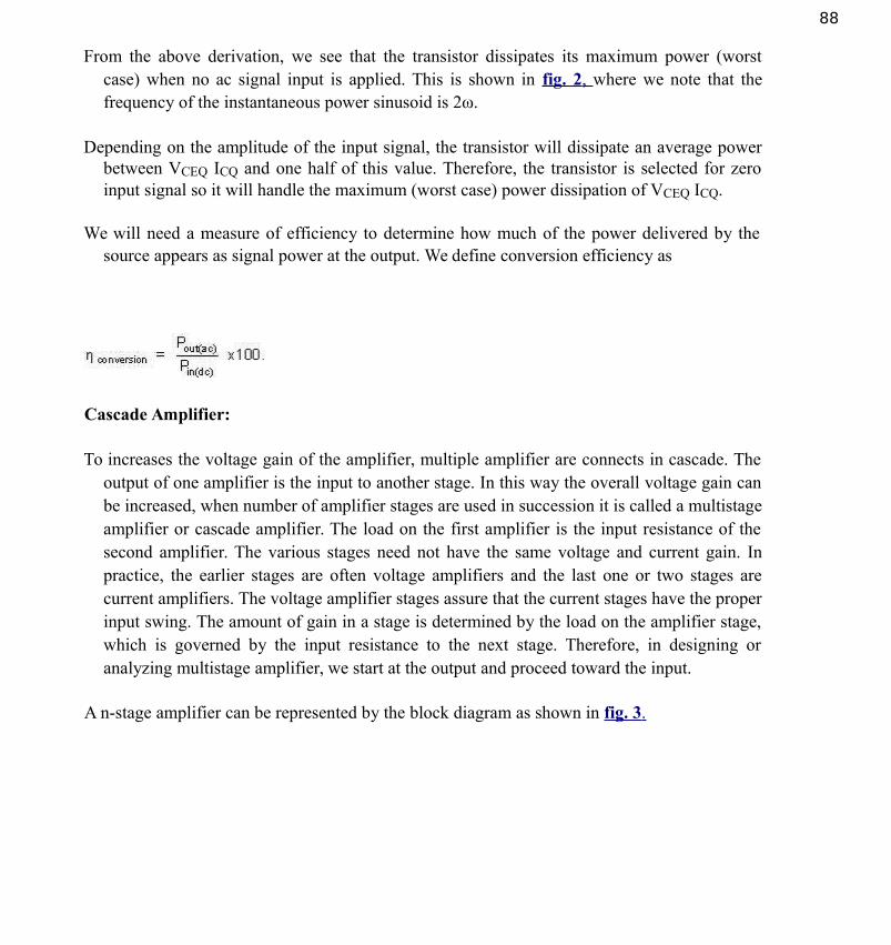
From the above derivation, we see that the transistor dissipates its maximum power (worstcase) when no ac signal input is applied. This is shown in fig. 2 , where we note that thefrequency of the instantaneous power sinusoid is 2ω.
Depending on the amplitude of the input signal, the transistor will dissipate an average powerbetween VCEQ ICQ and one half of this value. Therefore, the transistor is selected for zeroinput signal so it will handle the maximum (worst case) power dissipation of VCEQ ICQ.
We will need a measure of efficiency to determine how much of the power delivered by thesource appears as signal power at the output. We define conversion efficiency as
Cascade Amplifier:
To increases the voltage gain of the amplifier, multiple amplifier are connects in cascade. Theoutput of one amplifier is the input to another stage. In this way the overall voltage gain canbe increased, when number of amplifier stages are used in succession it is called a multistageamplifier or cascade amplifier. The load on the first amplifier is the input resistance of thesecond amplifier. The various stages need not have the same voltage and current gain. Inpractice, the earlier stages are often voltage amplifiers and the last one or two stages arecurrent amplifiers. The voltage amplifier stages assure that the current stages have the properinput swing. The amount of gain in a stage is determined by the load on the amplifier stage,which is governed by the input resistance to the next stage. Therefore, in designing oranalyzing multistage amplifier, we start at the output and proceed toward the input.
A n-stage amplifier can be represented by the block diagram as shown in fig. 3 .

89
Fig. 3
In fig. 3 , the overall voltage gain is the product of the voltage gain of each stage. That is, theoverall voltage gain is ABC.
To represent the gain of the cascade amplifier, the voltage gains are represents in dB. The twopower levels of input and output of an amplifier are compared on a logarithmic scale ratherthan linear scale. The number of bels by which the output power P2 exceeds the input power
P1 is defined as
Because of dB scale the gain can be directly added when a number of stages are cascaded.

90
Types of Coupling:
In a multistage amplifier the output of one stage makes the input of the next stage. Normally anetwork is used between two stages so that a minimum loss of voltage occurs when thesignal passes through this network to the next stage. Also the dc voltage at the output of onestage should not be permitted to go to the input of the next. Otherwise, the biasing of thenext stage are disturbed.
The three couplings generally used are.
1. RC coupling2. Impedance coupling3. Transformer coupling.
1.RC coupling:
Fig. 4 shows RC coupling the most commonly used method of coupling from one stage to thenext. An ac source with a source resistance R S drives the input of an amplifier. Thegrounded emitter stage amplifies the signal, which is then coupled to next CE stage thesignal is further amplified to get larger output.
In this case the signal developed across the collector resistor of each stage is coupled into thebase of the next stage. The cascaded stages amplify the signal and the overall gain equals theproduct of the individual gains.
Fig. 4

91
The coupling capacitors pass ac but block dc Because of this the stages are isolated as for as dcis concerned. This is necessary to avoid shifting of Q-points. The drawback of this approachis the lower frequency limit imposed by the coupling capacitor.
The bypass capacitors are needed because they bypass the emitters to ground. Without them,the voltage gain of each stage would be lost. These bypass capacitors also place a lowerlimit on the frequency response. As the frequency keeps decreasing, a point is reached atwhich capacitors no longer look like a.c. shorts. At this frequency the voltage gain starts todecrease because of the local feedback and the overall gain of the amplifier dropssignificantly. These amplifiers are suitable for frequencies above 10 Hz.
Example - 1
Determine the current and voltage gains for the two-stage capacitor-coupled amplifier shown infig. 1 .
Fig. 1
Solution:
We develop the hybrid equivalent circuit for the multistage amplifier. This equivalent is shownin fig. 2 . Primed variables denote output stage quantities and unprimed variables denoteinput stage quantities.

92
Fig. 2
Calculations for the output stages are as follows
For the input stage,

93
The input resistance is determined as:
The current gain, Ai, can be found by applying the equations derived earlier, where the first
stage requires using the correct value for Rload derived form the value of Rin to the nextstage.
Alternatively, we analyze fig. 2 by extracting four current dividers as shown in fig. 3 .
Fig. 3
The current division of the input stage is
The output of the first stage is coupled to the input of he second stage in fig. 3(b) . The inputresistance of the second stage is
The current in R'in is iload and is given by

94
Again, i load is current-divided at the input to the second stage. Thus,
The output current is found from fig. 3(c):
The current gain is then
Ai =927
Now using the gain impedance formula, we find the voltage gain:
Impedance Coupling:
At higher frequency impedance coupling is used. The collector resistance is replaced by an
inductor as shown in fig. 4 . As the frequency increases, XL approaches infinity and eachinductor appears open. In other words, inductors pass dc but block ac. When used in thisway, the inductors are called RFchokes.

95
The advantage is that no signal power is wasted in collector resistors. These RF chokes arerelatively expensive and their impedance drops off at lower frequencies. It is suitable atradio frequency above 20 KHz.
Transformer Coupling:
In this case a transformer is used to transfer the ac output voltage of the first stage to the input
of the second stage. Fig. 5 , the resistors RC is replaced by the primary winding of thetransformer. The secondary winding is used to give input to next stage. There is no couplingcapacitor. The dc isolation between the two stages provided by the transformer itself. Thereis no power loss in primary winding because of low resistance.
Fig. 5
At low frequency the size and cost of the transformer increases. Transformer coupling is stillused in RF amplifiers. In AM radio receivers, RF signal have frequencies 550 to 1600 KHz.In TV receivers, the frequencies are 54 to 216 MHz. At these frequency the size and cost of
the transformer reduces. CS capacitor is used to make other point of transformer grounded,so that ac signal is applied between base and ground.
Tuned Transformer Coupling:
In this case a capacitor is shunted across primary winding to get resonance as shown in fig. 6 .At this frequency the gain is maximum and at other frequencies the gain reduces very much.

96
This allows us to filter out all frequencies except the resonant frequency and those near it.This is the principle behind tuning in a radio station or TV channel.
Fig. 6
Example - 2
Design a transformer-coupled amplifier as shown in fig. 7 for a current gain of Ai = 80. Find
the power supplied to the load and the power required from the supply.
Fig. 7
Solution:
We first use the design equation to find the location of the Q-point for maximum output swing.
97
Since the problem statement requires a current gain of 80, the amplifier must have a currentgain of 10 because the transformer provides an additional gain of 8. We use the equations
from Chapter 5 to find the base resistance RB,
We note that re is sufficiently small to be neglected. Then, solving for RB yields
Now solving for the bias resistors,
The design is now complete. The power delivered by the source is given by
The power dissipated in the load is
We have restricted operation to the linear region by eliminating 5% of the maximum swingnear cutoff and saturation. The efficiency is the ratio of the load to source power.

98
Module-4
Power Amplifier
The amplifiers in multistage amplifier near the load end in almost all-electronic system employlarge signal amplifiers (Power amplifiers) and the purpose of these amplifiers is to obtainpower again.
Consider the case of radio receiver, the purpose of a radio receiver is to produce the transmittedprogrammes with sufficient loudness. Since the radio signal received at the receiver output isof very low power, therefore, power amplifiers are used to put sufficient power into thesignal. But these amplifier need large voltage input.
Therefore, it is necessary to amplify the magnitude of input signal by means of smallamplifiers to a level that is sufficient to drive the power amplifier stages.
In multistage amplifier, the emphasis is on power gain in amplifier near the load. In theseamplifies, the collector currents are much larger because the load resistances are small (i.eimpedence of loud speaker is 3.2 ohm).
A power amplifier draws a large amount of dc power form dc source and convert it into signalpower. Thus, a power amplifier does not truly amplify the signal power but converts the dcpower into signal power.
DC and AC load lines:
Consider a CE amplifier as shown in fig. 1 .
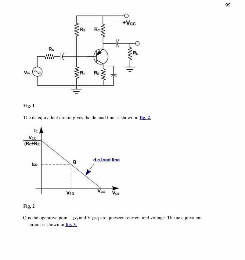
99
Fig. 1
The dc equivalent circuit gives the dc load line as shown in fig. 2 .
Fig. 2
Q is the operative point. ICQ and V CEQ are quiescent current and voltage. The ac equivalent
circuit is shown in fig. 3 .

100
Fig. 3
This circuit produces ac load line. When no signal is present, the transistor operates at the Qpoint shown in fig. 4 .
Fig. 4
When a signal is present, operating point swings along the ac load line rather than dc load line.The saturation and cut off points on the ac load line are different from those on the dc loadline.
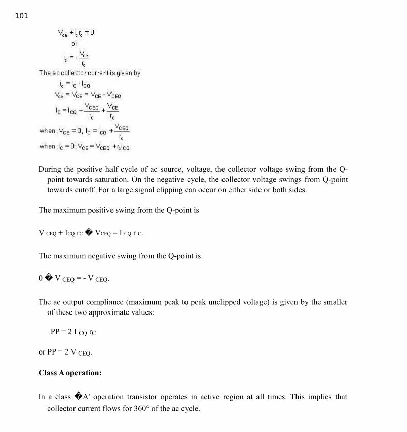
101
During the positive half cycle of ac source, voltage, the collector voltage swing from the Q-point towards saturation. On the negative cycle, the collector voltage swings from Q-pointtowards cutoff. For a large signal clipping can occur on either side or both sides.
The maximum positive swing from the Q-point is
V CEQ + ICQ rC � VCEQ = I CQ r C.
The maximum negative swing from the Q-point is
0 � V CEQ = - V CEQ.
The ac output compliance (maximum peak to peak unclipped voltage) is given by the smallerof these two approximate values:
PP = 2 I CQ rC
or PP = 2 V CEQ.
Class A operation:
In a class �A' operation transistor operates in active region at all times. This implies that
collector current flows for 360° of the ac cycle.

Voltage gain of loaded amplifier
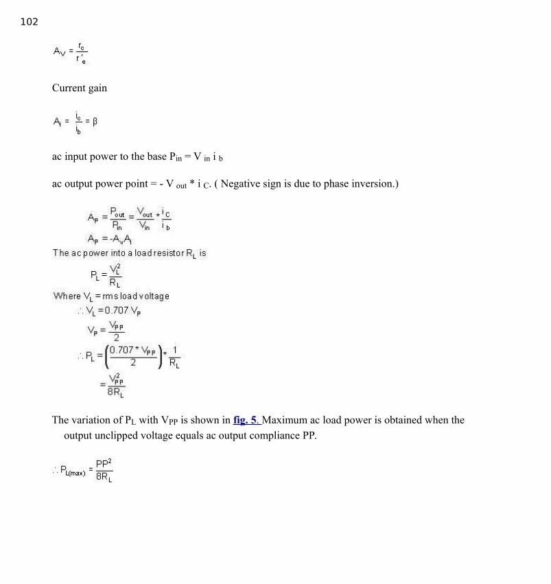
102
Current gain
ac input power to the base Pin = V in i b
ac output power point = - V out * i C. ( Negative sign is due to phase inversion.)
The variation of PL with VPP is shown in fig. 5 . Maximum ac load power is obtained when the
output unclipped voltage equals ac output compliance PP.
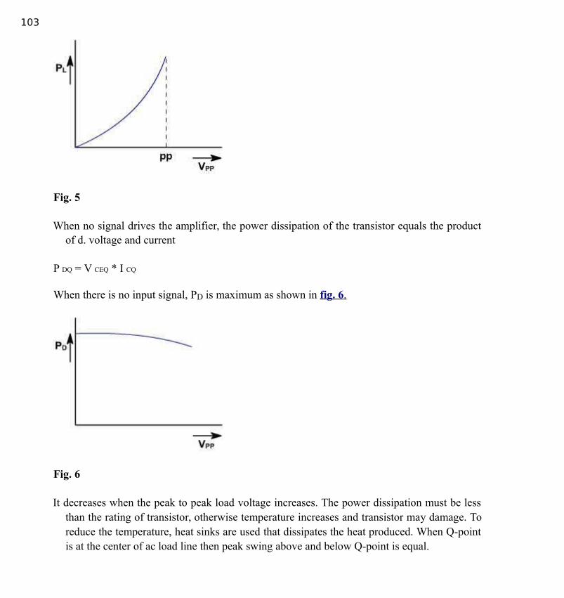
103
Fig. 5
When no signal drives the amplifier, the power dissipation of the transistor equals the productof d. voltage and current
P DQ = V CEQ * I CQ
When there is no input signal, PD is maximum as shown in fig. 6 .
Fig. 6
It decreases when the peak to peak load voltage increases. The power dissipation must be lessthan the rating of transistor, otherwise temperature increases and transistor may damage. Toreduce the temperature, heat sinks are used that dissipates the heat produced. When Q-pointis at the center of ac load line then peak swing above and below Q-point is equal.

104
Class A current drain:
In a class A amplifier shown in fig.1 , the dc source VCC must supply direct current to the
voltage divider and the collector circuit.
Fig. 1
Assuming a stiff voltage divider circuit, the dc current drain of the voltage divider circuit is
I 1 = V CC / (R 1 +R 2 )
In the collector circuit, the dc current drain is
I 2 = I CQ

105
In a class A amplifier, the sinusoidal variations in collector current averages to zero. Therefore,whether the ac signal is present or not, the dc source must supply an average current of
I S = I 1 + I 2.
This is the total dc current drain. The dc source voltage multiplied by the dc current drain givesthe ac power supplied to an amplifier.
P S = V CC IS
Therefore, efficiency of the amplifier, = (P L (max) / P S ) * 100 %
Where,, P L (max) = maximum ac load line power. In class A amplifier, there is a wastage of
power in resistor R C and R E i.e. ICQ 2 * (R C + R E ).
To reduce this wastage of power R C and R E should be made zero. R E cannot be made zero
because this will give rise to bias stability problem. R C can also not be made zero becauseeffective load resistance gets shorted. This results in more current and no power transfer to
the load R L. The R C resistance can, however, be replaced by an inductance whose dcresistance is zero and there is no dc voltage drop across the choke as shown in fig. 1 .
Since in most application the load is loudspeaker, therefore power amplifier drives theloudspeaker, and the maximum power transfer takes place only when load impedence isequal to the source impedence. If it is not, the loud speaker gets less power. The impedencematching is done with the help of transformer, as shown in fig. 2 .
Fig. 2

106
The ratio of number of turns is so selected that the impedence referred to primary side can bematched with the output impedence of the amplifier.
Class B amplifier:
The efficiency ( ) of class A amplifier is poor. The reason is that these circuits drawconsiderable current from the supply even in the absence of input signals.
In class B operation the transistor collector current flows for only 180° of the ac cycle. Thisimplies that the Q-point is located approximately at cutoff on both dc and ac load lines. Theadvantages of class B operation are
Lower transistor power dissipationReduced current drain.Eficiency is given by
Value is around 70%
Push pull circuit:
When a transistor operates in class B, itclips off a half cycle. To avoid theresulting distortion, two transistors are
used in push pull arrangement. This Fig. 3means that one transistor conductsduring positive half cycle and other

107
transistor conducts during negative halfcycle. The distortion is low, load poweris large and efficiency ( ) ismore. fig. 3 , shows how a npn and pnptransistor emitter followers are
connected in push pull arrangement.
The dc & ac equivalent circuit are shownin fig. 4 & fig. 5 . The biasing resistorsare selected so that Q-point is set atcutoff. This biases the emitter diode ofeach transistor between 0.6V and 0.7V
i.e. I CQ = 0.
Because the biasing resistors are equaleach emitter diode is biased with thesame voltage. As a result half the
supply voltage is dropped across eachtransistor.
VCEQ = VCC / 2.

Fig. 4 Fig. 5

108
Since there is no dc resistance in the collector or emitter circuits, the dc saturation current isinfinite. The dc load line is vertical as shown in fig. 6. The most difficult thing is setting up a
stable Q-point at cut off. Any significant increase in V BE with temperature can move the Q-point up the dc load line to dangerously high currents. Ac load line is given by
I C(sat) = I CQ + (V CEQ / r E )
V CE (cut off) = V CEQ + I CQ r E
I CQ = 0; V CEQ = V CC / 2
i.e. I C(sat) = V CC / 2RL ( i.e. rE = R L )
V CE (cut off) = V CC / 2.
Fig. 6
When either transistor is conducting, that transistor's operating point swings along the ac loadline and the operating point of the other transistor remains at cut off. The voltage swing ofthe conducting transistor can go from cut off to saturation. In the next half cycle, the othertransistor does the same thing.
Therefore, PP = VCC
Voltage gain of loaded amplifier:
AV= R L / (R L + r'e )
Z in (base) (RL + r'e )
Z out = r'e + (r B ) /
A P =A V * Ai
Without signal the capacitor charges up to VCC / 2 relative to ground.
In the positive half cycle of input voltage, the upper transistor conducts and the lower one cutoff. The upper transistor acts like an ordinary emitter follower, so that the output voltage

109
approximately equals the input voltage. The current flow through RL is such as direct as to
make output positive.
In the negative half cycle of input voltage, the upper transistor cuts off and the lower transistorconducts. The lower transistor acts like an ordinary emitter follower and produces a loadvoltage approximately equal to the input voltage (i.e. negative output. Since Q, is off, no
current can flow from VCC through Q, but capacitor acts like a battery source anddischarges).
During either half cycle, the source sees a high input impedence looking into either base andthe load sees a low output impedence.
Cross over distortion:
Fig. 1 shows the ac equivalent circuit of a class B push pull amplifier. Suppose that no bias isapplied to the emitter diodes. Then the incoming voltage has to rise to about 0.7 V to overcomethe barrier potential. Because of this no current flows through Q, when the signal is less than 0.7
V. The action is similar on the other half cycle no current flows in Q2 until ac
voltage is more negative the � 0.7 V. If no bias is applied the output of class B amplifier
looks like as shown in fig. 1.
Fig. 1
The signal output is distorted. Because of clipping action between half cycles, it no longer is asine wave. Since the clipping occurs between the time one transistor cuts off and the timethe other comes on, it is called cross over distortion. To eliminate cross over distortion, theslight forward bias must be applied to each emitter diode. This means locating the Q-point

110
slightly above cut off as shown in fig. 2 . In fact, this is class AB operation. This means that collector current flows for more than 180 degrees but less than 360°.
Fig. 2
Class A amplifier introduces non-linear distortion in input wave means elongates one half cycleand compresses one half cycle. This can be reduced by swamping. In this case it can befurther reduced because both half cycles are identical in shape, is given by non-lineardistortion is much less than class A.
Load power is given by
Since the ac output compliance equals the peak-to-peak voltage, the maximum load power is
Where, I1 = current through biasing resistance. When no signal is present I2 = ICQ and thecurrent drain is small. But when a signal is present, the current drain increase because theupper collector current becomes large.

111
If the entire ac load line is used, then the upper transistor has a half sine wave of currentthrough it with a peak value of
IC(sat) = VCEQ / RL
The average value of half sine wave is given by
The dc power is supplied to the circuit is PS = VCC is under no signal conditions, the dc poweris small because the current drain is minimum. But when a signal uses the entire ac loadline, the dc power supplied to the circuit reaches a maximum.
Biasing a class B amplifier:
In class B amplifier, two complement any transistors are required. Because of the seriesconnection, each transistor drops half the supply voltage. To avoid cross over distortion, the
Q-point slightly above cut off, with the correct VBE somewhere between 0.6 and 0.7.
If there is an increase in VBE by few mV it produces 10 times as much emitter current. Because
of this it is difficult to find standard resistors that can produce the correct VBE and it needsan adjustable resistor.
The biasing does not solve thermal instability problem. Because for a given collector current,
VBE requirement decreases by 2 mV per degree rise in temperature. The voltage dividerproduces a stiff drive for each diode. Therefore as the temperature increases, the fixedvoltage on each emitter diode forces the collector current to increase and this gives rise tothermal run away. When the temperature increases collector current increases, and this isequivalent to Q-point moving up along the vertical dc load line. As the Q-point movestoward higher collector currents, the temperature of the transistor increases further reducing
the required V BE .

112
Fig. 3
One way to avoid thermal run away is to use diode bias. It is based on the concept of currentmirror as shown in fig. 3 , the base current is much smaller than the current through theresistor and diode. For this reason, I1 and I2 are approximately equal. If the diode curve isidentical to the VBE curve of the transistor (VBE , IE ). The diode current equals the emitterand also collector current. Therefore I1 is nearly equal to IC.
I1 = I C .
The collector current is set by controlling the resistor current. This is called a current mirror.
Similarly, pnp transistor can be used as a current mirror. If the VBE curve of the transistor
matches the diode curve, the collector equals the resistor current.
Diode bias of class B push pull emitter follower relies on two current mirrors as shown in fig.4 .

113
Fig. 4
The upper half is an npn current mirror, and the lower half is a pnp current mirror as shown infig. 4 . For diode bias to be immune to changes in temperature, the diode curve must match
the VBE curves of the transistor over a wide temperature range. This is easily done in ICs .
Power Calculations for Class B Push-Pull Amplifier
The power delivered by the ac source is split between the transistor and the resistors in the biascircuitry. The ac signal source adds an insignificant additional amunt of power since basecurrents are small relative to collector currents. Part of the power to the transistor goes toload, and the other part is dissipated by the transistor itself. The following equations specifythe various power relationships in the circuit.
The average power supplied by the dc source is

114
iCC(t) is the total current and is composed of two components: the dc current through the base
bias resistor and diode combination, and the ac collector current through transistor, Q1.
Under quiescent conditions (i.e. zero input) Q1 is in cutoff mode. Collector current flowsduring the positive half of the output signal waveform. Therefore we only need to integratethis component of the power supply signal over the first half cycle.
The maximum values of collector current and power delivered to the transistor are
The ac output power, assuming a sinusoidal input, is
The maximum ac output power is found by substituting ICmax for IC1max to get
The total power supplied to the stage is the sum of the power to the transistor and the power tothe bias and compensation circuitry.
If we subtract the power to the load from the power supplied to the transistors, we find thepower being dissipated in the transistors the power dissipated by a single transistor is onehalf of this value. Thus,

115
we are assuming that the base current is negligible. The efficiency of the Class B push-pullamplifier is the ratio of the output power to the power delivered to the transistor. Thus weneglect the power dissipated by the bias circuitry.
This amplifier is more efficient than a Class A amplifier. It is often used in output circuitswhere efficiency important design requirement.
Therefore,
In choosing a transistor, it is important that the power rating is equal to or exceeds themaximum power Pmax.
Class C amplifier:
A class C amplifier can produce more power than a class B amplifier.
Consider the case of a radio transmitter in which the audio signals are raised in their frequencyto the medium or short wave band to that they can be easily transmitted. The high frequencyintroduced is in radio frequency range and it serves as the carrier of the audio signal. Theprocess of raising the audio signal to radio frequency called modulation.
The modulated wave has a relatively narrow band of frequencies centered around the carrierfrequencies. At any instant, there are several transmitter transmitting programmessimultaneously. The radio receiver selects the signals of desired frequencies to which it istuned, amplifies it and converts it back to audio range. Therefore, tuned voltage amplifiersare used. In short, the tuned voltage amplifiers selects the desired radio frequency signal outof a number of RF signals present at that instant and then amplifies the selected RF signal tothe desired level as shown in fig. 1 .

116
Fig. 1
Class C operation means that the collector current flows for less than 180° of the ac cycle. Thisimplies that the collector current of a class C amplifier is highly non-sinusoidal becausecurrent flows in pulses. To avoid distortion, class C amplifier makes use of a resonant tankcircuit. This results in a sinusoidal output voltage.
The resonant tank circuit is tuned to the frequency of the input signal. When the circuit has ahigh quality factor (Q) parallel resonance occurs at approximately
At the resonance frequency, the impedence of the parallel resonant circuit is very high asshown in fig. 2 and is purely resistive. When the circuit is tuned to the resonant frequency,
the voltage across RL is maximum and sinusoidal. The higher the Q of the circuit, the fasterthe gain drops off on either side of resonance

117
Fig. 2
Fig. 3
The dc equivalent circuit is shown fig. 3 . No bias is applied to the transistor. Therefore, its Q-
point is at cut off on the dc load line VBE= 0.7V. Therefore no IL current flows until input is
more than 0.7 V. Also dc resistance is RS (the resistance of inductor) which is very small andtherefore dc load line is almost vertical. There is no danger of thermal runway because thereis no current other than from leakage.
The IC(sat) current is given by
where rC is the collector resistance.

118
The voltage VCE(sate) is given by
when ICQ = 0, VCEQ = VCC
When the Q of a resonant circuit is greater than 10. One can use the approximate ac equivalentcircuit. The series resistance of the inductor is lumped into the collector resistance. Atresonance, the peak-to-peak load voltage reaches a maximum. The bandwidth of a resonantcircuit is given by
Band width (BW) = f 2 � f 1
f 1 = Lower cut off frequency.
f 2 = Upper cut off frequency
The bandwidth is related to the resonant frequency and the circuit Q as below:
BW = f r / Q
This means a large Q produces small BW equivalent to sharp tuning. These amplifiers have Qgreater than 10. This means that the BW is less than 10% of the resonant frequencies. Theseamplifiers are also called narrow band amplifier.
When the tank circuit is resonant the ac load impedence seen by the collector current source ispurely resistive and the collector current is minimum. Above and below resonance, the acload impedence decreases and the collector current decreases. Any coil or inductor has some
series resistance RS as shown in fig. 4 .
The Q of all coil is given by.
Q L = X L / R L

119
Fig. 4
The series resistance can be replaced by parallel resistance RP . This equivalent resistance is
given by
R P = Q L RL
Now all the losses in the coil are now being represented by the parallel resistance RP and seriesresistance RS no longer exists XC cancels XL at resonance. Leaving only RP in parallel withRL.
Therefore,
RC = RP || RL
Q of the overall circuit = rC / XL
At the resonance frequency, the impedence of the parallel resonant circuit is very high asshown in fig. 2 and is purely resistive. When the circuit is tuned to the resonant frequency,
the voltage across RL is maximum and sinusoidal. The higher the Q of the circuit, the fasterthe gain drops off on either side of resonance
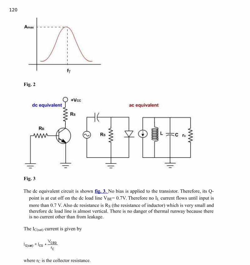
120
Fig. 2
Fig. 3
The dc equivalent circuit is shown fig. 3 . No bias is applied to the transistor. Therefore, its Q-
point is at cut off on the dc load line VBE= 0.7V. Therefore no IL current flows until input is
more than 0.7 V. Also dc resistance is RS (the resistance of inductor) which is very small andtherefore dc load line is almost vertical. There is no danger of thermal runway because thereis no current other than from leakage.
The IC(sat) current is given by
where rC is the collector resistance.

121
The voltage VCE(sate) is given by
when ICQ = 0, VCEQ = VCC
When the Q of a resonant circuit is greater than 10. One can use the approximate ac equivalentcircuit. The series resistance of the inductor is lumped into the collector resistance. Atresonance, the peak-to-peak load voltage reaches a maximum. The bandwidth of a resonantcircuit is given by
Band width (BW) = f 2 � f 1
f 1 = Lower cut off frequency.
f 2 = Upper cut off frequency
The bandwidth is related to the resonant frequency and the circuit Q as below:
BW = f r / Q
This means a large Q produces small BW equivalent to sharp tuning. These amplifiers have Qgreater than 10. This means that the BW is less than 10% of the resonant frequencies. Theseamplifiers are also called narrow band amplifier.
When the tank circuit is resonant the ac load impedence seen by the collector current source ispurely resistive and the collector current is minimum. Above and below resonance, the acload impedence decreases and the collector current decreases. Any coil or inductor has some
series resistance RS as shown in fig. 4 .
The Q of all coil is given by.
Q L = X L / R L

122
Fig. 4
The series resistance can be replaced by parallel resistance RP . This equivalent resistance is
given by
R P = Q L RL
Now all the losses in the coil are now being represented by the parallel resistance RP and seriesresistance RS no longer exists XC cancels XL at resonance. Leaving only RP in parallel withRL.
Therefore,
RC = RP || RL
Q of the overall circuit = rC / XL
Current Sources
There are different methods of simulating a dc current source for integrated circuit amplifierbiasing. One type of current source used to provide a fixed current is the fixed bias transistorcircuit. The problem with this type of current source is that it requires too many resistors tobe practically implemented on IC. The resistors in the following circuits are small and easyto fabricate on IC chips. When the current source is used to replace a large resistor theThevenin resistance of the current source is the equivalent resistance value.
A simple current source
The simple two transistor current source shown in fig. 1 is commonly used in ICs.
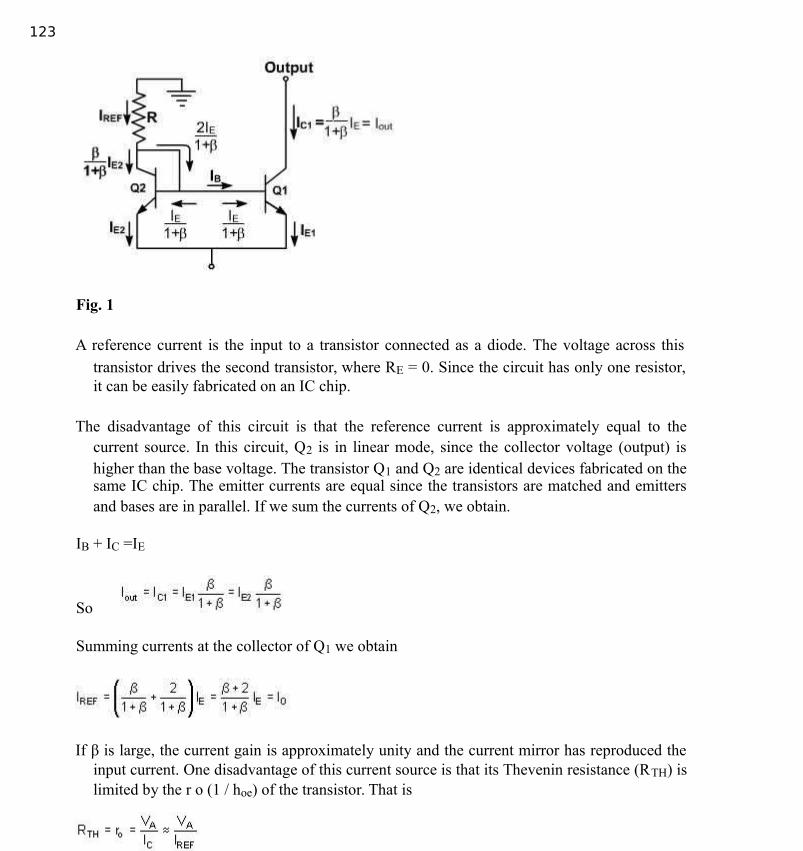
123
Fig. 1
A reference current is the input to a transistor connected as a diode. The voltage across this
transistor drives the second transistor, where RE = 0. Since the circuit has only one resistor,it can be easily fabricated on an IC chip.
The disadvantage of this circuit is that the reference current is approximately equal to thecurrent source. In this circuit, Q2 is in linear mode, since the collector voltage (output) ishigher than the base voltage. The transistor Q1 and Q2 are identical devices fabricated on thesame IC chip. The emitter currents are equal since the transistors are matched and emittersand bases are in parallel. If we sum the currents of Q2, we obtain.
IB + IC =IE
So
Summing currents at the collector of Q1 we obtain
If β is large, the current gain is approximately unity and the current mirror has reproduced theinput current. One disadvantage of this current source is that its Thevenin resistance (RTH) islimited by the r o (1 / hoe) of the transistor. That is

124
Widlar Current Source
Large resistors are often required to maintain small currents of the order of few �A and these
large resistors occupy correspondingly large areas on the IC chip. It is therefore, desirable toreplace these large resistors with current sources. One such device is the Widlar currentsource as shown in fig. 2 .
The two transistors are assumed perfectly matched. For the base circuit,
(E-4)
For a forward biased base-emitter junction diode, the emitter current is given by
Since iE ≈ iC = IC and n = 1
Fig. 2
and (E-5)
Substituting VBE1 and VBE2 from (E-5) to (E-4), we get
(E-6)
We have assumed that both the transistors are matched so that ICO, β and VT are the same for
both the transistors. Thus

125
Hence, (E-7)
where, (E-8)
For design purposes, IC1 is usually known since it is used as the reference for all current
sources on the entire chip and IC2 is t he desired output current. The Widlar circuit can alsobe used to simulate a high resistance.
Example-1
Design a Widlar current source to provide a constant current source of 3 �A with VCC = 12V,
R1 = 50 kO, β =100 and VBE = 0.7V
Solution:
The circuit is given in fig.2 . Applying KVL to the Q1 transistor we get,
Using the equation (E-7) we can calculate R2
or R2 = 36 kΩ
Wilson Current Source
Another current source transistor configuration that provides a very large parallel resistance isthe Wilson current source which uses three transistors and provides this capability an theoutput is almost independent of the internal transistor characteristics. The Wilson current
source as shown in fig. 3 , uses the negative feedback provided by Q3 to raise the outputimpedance

126
Fig. 3
The difference between the reference current and IC1 is the base current of Q2.
IE2 =(β + 1) IB2 = IC3 (E-9)
Since the base of Q1 is connected to the base of Q3, the currents in Q1 are approximately
independent of the voltage of the collector of Q2. As such, the collector current of Q2
remains almost constant providing high output impedance.
Let us now see that IC2 is approximately equal to IREF. Applying Kirchhoff's current law at the
emitter of Q2 yields
IE2 = IC3 + IB3 + IB1 (E-10)
Using the relationship between collector and base currents
(E-11)
Since all three transistors are matched, VBE1= VBE2 = VBE3 and β1 = β2 = β3
With identical transistors, current in the feedback path splits equally between the bases of Q1
and Q3 leading so that IB1 = IB3 and therefore IC1 = IC3. Thus, the emitter current of Q2becomes

127
(E-12)
The collector current of Q2 is
(E-13)
Solving for IC3 yields
(E-14)
Summing currents at the base of Q2,
(E-15)
(E-16)
Since IC1 = IC3, we substitute IC3 to obtain
(E-17)
and solving for IC2
(E-18)
Equation (E-10) shows that β has little effect upon IC2 since, for reasonable values of β.
(E-19)
Therefore, IC2 = IREF

Multiple Current sources Using Current Mirrors

128
A number of current sources can be obtained from a single reference voltage. If the current isapproximately the same as the reference voltage, the simple current source can be used as
shown in fig. 4 for Q2 and Q3.
Fig. 4
Notice that Q4 has an emitter resistance, which makes the current source a Widlar currentsource. Thus the amount of current delivered by this source can be determined by the size ofthe emitter resistor. This type of circuit is useful in integrated circuit chips as the onereference circuit can be used to develop current sources throughout the chip. When using theWidlar circuit, the currents can be different from the reference current.
The errors in base current, however, do accumulate when multiple outputs are used and thecurrent gain tends to deviate from unity. In these types of circuits, lateral transistors can beused since it is not important that b be large. Lateral transistors usually have a β ofapproximately 20 which is more than adequate for current sources.
Example -2:
For the circuit shown in fig. 5 , determine the emitter current in transistor Q3. Given that β =
100, VBE = 0.715V.

129
Fig. 5
Solution:
Since all transistor are identical, there VBE voltage drop will be same.
Let IB be the base current of each transistor and IC be the collector current of Q1 and Q2.
Therefore,
Example - 1
Determine the current and voltage gains for the two-stage capacitor-coupled amplifier shown infig. 1 .

130
Fig. 1
Solution:
We develop the hybrid equivalent circuit for the multistage amplifier. This equivalent is shownin fig. 2 . Primed variables denote output stage quantities and unprimed variables denoteinput stage quantities.
Fig. 2
Calculations for the output stages are as follows

131
For the input stage,
The input resistance is determined as:
The current gain, Ai, can be found by applying the equations derived earlier, where the first
stage requires using the correct value for Rload derived form the value of Rin to the nextstage.
Alternatively, we analyze fig. 2 by extracting four current dividers as shown in fig. 3 .

132
Fig. 3
The current division of the input stage is
The output of the first stage is coupled to the input of he second stage in fig. 3(b) . The input resistance of the second stage is
The current in R'in is iload and is given by
Again, i load is current-divided at the input to the second stage. Thus,
The output current is found from fig. 3(c):
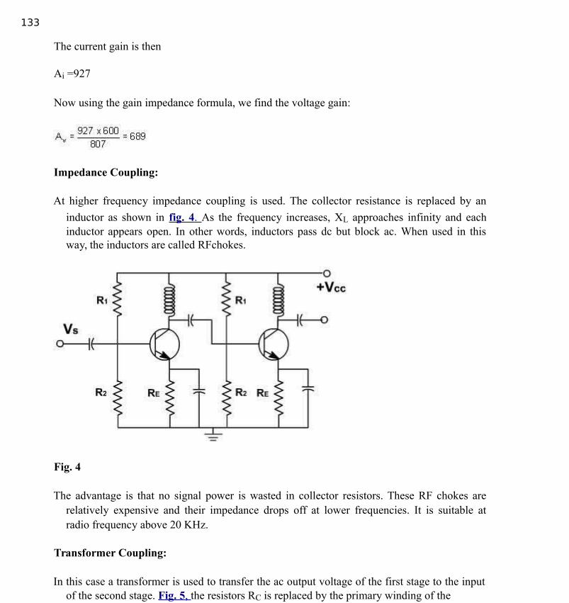
133
The current gain is then
Ai =927
Now using the gain impedance formula, we find the voltage gain:
Impedance Coupling:
At higher frequency impedance coupling is used. The collector resistance is replaced by an
inductor as shown in fig. 4 . As the frequency increases, XL approaches infinity and eachinductor appears open. In other words, inductors pass dc but block ac. When used in thisway, the inductors are called RFchokes.
Fig. 4
The advantage is that no signal power is wasted in collector resistors. These RF chokes arerelatively expensive and their impedance drops off at lower frequencies. It is suitable atradio frequency above 20 KHz.
Transformer Coupling:
In this case a transformer is used to transfer the ac output voltage of the first stage to the inputof the second stage. Fig. 5 , the resistors RC is replaced by the primary winding of the

134
transformer. The secondary winding is used to give input to next stage. There is no couplingcapacitor. The dc isolation between the two stages provided by the transformer itself. Thereis no power loss in primary winding because of low resistance.
Fig. 5
At low frequency the size and cost of the transformer increases. Transformer coupling is stillused in RF amplifiers. In AM radio receivers, RF signal have frequencies 550 to 1600 KHz.In TV receivers, the frequencies are 54 to 216 MHz. At these frequency the size and cost of
the transformer reduces. CS capacitor is used to make other point of transformer grounded,so that ac signal is applied between base and ground.
Tuned Transformer Coupling:
In this case a capacitor is shunted across primary winding to get resonance as shown in fig. 6 .At this frequency the gain is maximum and at other frequencies the gain reduces very much.This allows us to filter out all frequencies except the resonant frequency and those near it.This is the principle behind tuning in a radio station or TV channel.

135
Fig. 6
Example - 2
Design a transformer-coupled amplifier as shown in fig. 7 for a current gain of Ai = 80. Find
the power supplied to the load and the power required from the supply.
Fig. 7
Solution:
We first use the design equation to find the location of the Q-point for maximum output swing.

136
Since the problem statement requires a current gain of 80, the amplifier must have a currentgain of 10 because the transformer provides an additional gain of 8. We use the equations
from Chapter 5 to find the base resistance RB,
We note that re is sufficiently small to be neglected. Then, solving for RB yields
Now solving for the bias resistors,
The design is now complete. The power delivered by the source is given by
The power dissipated in the load is
We have restricted operation to the linear region by eliminating 5% of the maximum swingnear cutoff and saturation. The efficiency is the ratio of the load to source power.

137
Oscillators
Objectives:– To understand
• The basic operation of an Oscillator • the working of low frequency oscillators– RC phase shift oscillator – Wien bridge Oscillator• the working of tuned oscillator – Colpitt s Oscillator, Hartley Oscillator –‟ Crystal
Oscillator• the working of UJT Oscillator
Basic operation of an Oscillator
An amplifier with positive feedback results in oscillations if the followingconditions are satisfied:
– The loop gain ( product of the gain of the amplifier and the gain of the feedback network) is unity
– The total phase shift in the loop is 0
• If the output signal is sinusoidal, such a circuit is referred to as sinusoidal oscillator.
When the switch at the amplifier input is open, there are no oscillations. Imagine that a voltage Vi is fed to the circuit and the switch is closed. This results in V
When the switch at the amplifier input is open, there are no oscillations. Imagine that a voltage
Vi is fed to the circuit and the switch is closed. This results in and
is fed back to the circuit. If we make Vf = V then even if we remove the inputvoltage to the circuit, the output continues to exist.

138
then from the above equation, it is clear that, A =1V Thus in the above block diagram, by closing the switch and removing the input, we are able to get the oscillations at the output if AV =1, where A is called theLoop gain.
Positive feedback refers to the fact that the fed back signal is in phase with the input signal. This means that the signal experiences 0 phase shift while traveling in the loop. The above condition along with the unity loop gain needs to be satisfied to get the sustained oscillations. These conditions are referred to as „Barkhausen criterion . Another way of ‟seeing how the feedback circuit provides operation as an oscillator is obtained by noting thedenominator in the basic equation
Af = A / (1+ A).When A = -1 or magnitude 1 at a phase angle of 180 , the denominator becomes 0 and the gain with feedback Af becomes infinite.Thus, an infinitesimal signal ( noise voltage) can
provide a measurable output voltage, and the circuit acts as an oscillator even without aninput signal.
Phase shift oscillator
• The phaseshift oscillator utilizes three RC circuits to provide 180º phase shift that when coupled withthe 180º of the op-amp itself provides the necessary feedback to sustain oscillations.
• The gain must be at least 29 to maintain the oscillations. The frequency of resonance for the
this type is similar to any RC circuit oscillator:

139
• The amplifier stage is self biased with a capacitor bypassed source resistor Rs and a drain bias resistor Rd . The FET device parameters of interest are gm and rd.
• At the operating frequency, we can assume that the input impedance of theamplifier is infinite .
• This is a valid approximation provided, the oscillator operating frequency is low enough so that FET capacitive impedances can be neglected.
• The output impedance of the amplifier stage given by R should also be small compared to theimpedance seen looking into the feedback network so that no attenuation due to loading occurs.

140
• If a transistor is used as the active element of the amplifier stage, the output of thfeedback network is loaded appreciably by the relatively low input resistance ( h ie) of the transistor.
• An emitter – follower input stage followed by a common emitter amplifier stagecould be used.If a single transistor stage is desired, the use of voltage – shunt feedback is more
suitable. Here, the feedback signal is coupled through the feedback resistor R in series‟with the amplifier stage input resistance ( R i).
Problem:It is desired to design a phase shift oscillator using an FET having g = 5000 S rd= 40 k , and a
feedback circuit value of R = 10 k . Select the value of C for oscillator operation at 5 kHz and RD for A > 29 to ensure oscillator action.

141
Wien bridge oscillator
A Wien bridge oscillator is a type of electronic oscillator that generates sine waves. It can generate a large range of frequencies. The circuit is based on an electrical network originally developed by Max Wien in 1891. The bridge comprises four resistors and two capacitors. It can also be viewed as a positive feedback system combined with a bandpass filter. Wien did not have a means of developing electronic gain so a workable oscillator could not be realized.
The modern circuit is derived from William Hewlett's 1939 Stanford University master's degree thesis. Hewlett, along with David Packard co-founded Hewlett-Packard. Their first product was the HP 200A, a precision sine wave oscillator based on the Wien bridge.The 200A was one of the first instruments to produce such low distortion.
The frequency of oscillation is given by:

142
Analysis
Input admittance analysis
If a voltage source is applied directly to the input of an ideal amplifier with feedback, the inputcurrent will be:
Where vin is the input voltage, vout is the output voltage, and Zf is the feedback impedance.
If the voltage gain of the amplifier is defined as:
And the input admittance is defined as:

Input admittance can be rewritten as:
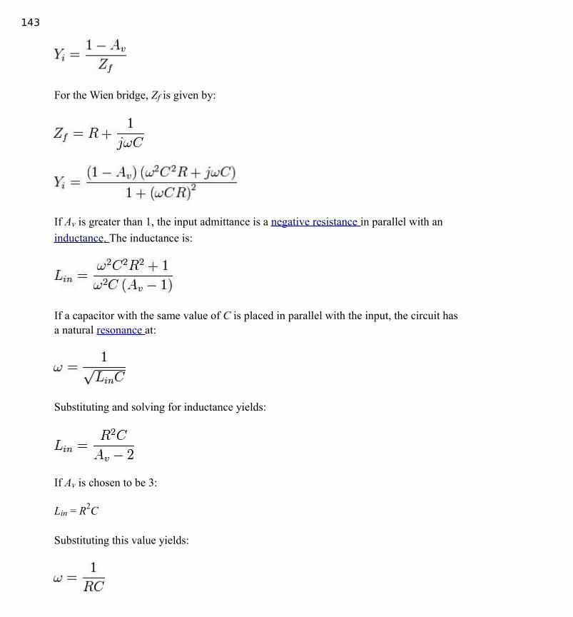
143
For the Wien bridge, Zf is given by:
If Av is greater than 1, the input admittance is a negative resistance in parallel with an
inductance . The inductance is:
If a capacitor with the same value of C is placed in parallel with the input, the circuit has a natural resonance at:
Substituting and solving for inductance yields:
If Av is chosen to be 3:
Lin = R2C
Substituting this value yields:

Or:

144
Similarly, the input resistance at the frequency above is:
For Av = 3:
Rin = − R
If a resistor is placed in parallel with the amplifier input, it will cancel some of the negative resistance. If the net resistance is negative, amplitude will grow until clipping occurs. Similarly, if the net resistance is positive, oscillation amplitude will decay. If a resistance is added in parallel with exactly the value of R, the net resistance will be infinite and the circuit can sustain stable oscillation at any amplitude allowed by the amplifier.
Notice that increasing the gain makes the net resistance more negative, which increases amplitude. If gain is reduced to exactly 3 when a suitable amplitude is reached, stable, low distortion oscillations will result. Amplitude stabilization circuits typically increase gain until a suitable output amplitude is reached. As long as R, C, and the amplifier are linear, distortion will be minimal.
Crystal oscillator
A crystal oscillator is an electronic circuit that uses the mechanical resonance of a vibrating crystal of piezoelectric material to create an electrical signal with a very precise frequency. This frequency is commonly used to keep track of time (as in quartz wristwatches), to providea stable clock signal for digital integrated circuits, and to stabilize frequencies for radio transmitters and receivers. The most common type of piezoelectric resonator used is the quartzcrystal , so oscillator circuits designed around them were called "crystal oscillators".
Quartz crystals are manufactured for frequencies from a few tens of kilohertz to tens of
megahertz. More than two billion (2×10⁹) crystals are manufactured annually. Most are small devices for consumer devices such as wristwatches, clocks, radios, computers, and cellphones.Quartz crystals are also found inside test and measurement equipment, such as counters, signal generators , and oscilloscopes

145
A quartz crystal can be modeled as an electrical network with a low impedance (series) and ahigh impedance (parallel) resonance point spaced closely together. Mathematically (using theLaplace transform) the impedance of this network can be written as:
or,
where s is the complex frequency (s = jω), ωs is the series resonant frequency in radians
per second and ωp is the parallel resonant frequency in radians per second.
Adding additional capacitance across a crystal will cause the parallel resonance to shift downward. This can be used to adjust the frequency at which a crystal oscillator oscillates. Crystalmanufacturers normally cut and trim their crystals to have a specified resonance frequency with a known 'load' capacitance added to the crystal. For example, a 6 pF 32 kHz crystal has a parallel resonance frequency of 32,768 Hz when a 6.0 pF capacitor is placed across the crystal. Without this capacitance, the resonance frequency is higher than 32,768 Hz.

146
Module-5
Field Effect Transistor
The field effect transistor is a semiconductor device, which depends for its operation on the control of current by an electric field. There are two of field effect transistors:
1. JFET (Junction Field Effect Transistor)2. MOSFET (Metal Oxide Semiconductor Field Effect Transistor)
The FET has several advantages over conventional transistor.
1. In a conventional transistor, the operation depends upon the flow of majority and minoritycarriers. That is why it is called bipolar transistor. In FET the operation depends upon the flowof majority carriers only. It is called unipolar device.
2. The input to conventional transistor amplifier involves a forward biased PN junction with itsinherently low dynamic impedance. The input to FET involves a reverse biased PN junctionhence the high input impedance of the order of M-ohm.
3. It is less noisy than a bipolar transistor.4. It exhibits no offset voltage at zero drain current.5. It has thermal stability.6. It is relatively immune to radiation.
The main disadvantage is its relatively small gain bandwidth product in comparison with conventional transistor.
Operation of FET:
Consider a sample bar of N-type semiconductor. This is called N-channel and it is electricallyequivalent to a resistance as shown in fig. 1
Fig. 1

147
Ohmic contacts are then added on each side of the channel to bring the external connection.Thus if a voltage is applied across the bar, the current flows through the channel.
The terminal from where the majority carriers (electrons) enter the channel is called sourcedesignated by S. The terminal through which majority carriers leaves the channel is calleddrain and designated by D. For an N-channel device, electrons are the majority carriers.
Hence the circuit behaves like a dc voltage VDS applied across a resistance RDS. The
resulting current is the drain current ID. If VDS increases, ID increases proportionally.
Now on both sides of the n-type bar heavily doped regions of p-type impurity have beenformed by any method for creating pn junction. These impurity regions are called gates(gate1 and gate2) as shown in fig. 2 .
Both the gates are internally connected and they are grounded yielding zero gate source voltage(VGS =0). The word gate is used because the potential applied between gate and sourcecontrols the channel width and hence the current.
As with all PN junctions, a depletion region is formed on the two sides of the reverse biasedPN junction. The current carriers have diffused across the junction, leaving only uncoveredpositive ions on the n side and negative ions on the p side. The depletion region widthincreases with the magnitude of reverse bias. The conductivity of this channel is normallyzero because of the unavailability of current carriers.
The potential at any point along the channel depends on the distance of that point from thedrain, points close to the drain are at a higher positive potential, relative to ground, thenpoints close to the source. Both depletion regions are therefore subject to greater reversevoltage near the drain. Therefore the depletion region width increases as we move towardsdrain. The flow of electrons from source to drain is now restricted to the narrow channelbetween the no conducting depletion regions. The width of this channel determines theresistance between drain and source.
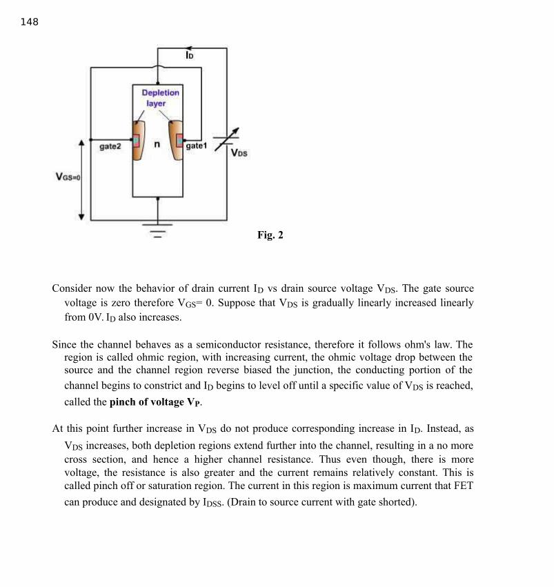
148
Fig. 2
Consider now the behavior of drain current ID vs drain source voltage VDS. The gate sourcevoltage is zero therefore VGS= 0. Suppose that VDS is gradually linearly increased linearlyfrom 0V. ID also increases.
Since the channel behaves as a semiconductor resistance, therefore it follows ohm's law. Theregion is called ohmic region, with increasing current, the ohmic voltage drop between thesource and the channel region reverse biased the junction, the conducting portion of the
channel begins to constrict and ID begins to level off until a specific value of VDS is reached,
called the pinch of voltage VP.
At this point further increase in VDS do not produce corresponding increase in ID. Instead, as
VDS increases, both depletion regions extend further into the channel, resulting in a no morecross section, and hence a higher channel resistance. Thus even though, there is morevoltage, the resistance is also greater and the current remains relatively constant. This iscalled pinch off or saturation region. The current in this region is maximum current that FET
can produce and designated by IDSS. (Drain to source current with gate shorted).

149
Fig. 3
As with all pn junctions, when the reverse voltage exceeds a certain level, avalanchebreakdown of pn junction occurs and ID rises very rapidly as shown in fig. 3 .
Consider now an N-channel JFET with a reverse gate source voltage as shown in fig. 4 .
Fig. 4Fig. 5
The additional reverse bias, pinch off will occur for smaller values of | VDS |, and the maximum
drain current will be smaller. A family of curves for different values of VGS(negative) isshown in fig. 5 .
Suppose that VGS= 0 and that due of VDS at a specific point along the channel is +5V with
respect to ground. Therefore reverse voltage across either p-n junction is now 5V. If VGS is

150
decreased from 0 to ?1V the net reverse bias near the point is 5 - (-1) = 6V. Thus for any fixed value of VDS, the channel width decreases as VGS is made more negative.
Thus ID value changes correspondingly. When the gate voltage is negative enough, thedepletion layers touch each other and the conducting channel pinches off (disappears). Inthis case the drain current is cut off. The gate voltage that produces cut off is symbolized
VGS(off) . It is same as pinch off voltage.
Since the gate source junction is a reverse biased silicon diode, only a very small reversecurrent flows through it. Ideally gate current is zero. As a result, all the free electrons from
the source go to the drain i.e. ID = IS. Because the gate draws almost negligible reversecurrent the input resistance is very high 10's or 100's of M ohm. Therefore where high inputimpedance is required, JFET is preferred over BJT. The disadvantage is less control overoutput current i.e. FET takes larger changes in input voltage to produce changes in outputcurrent. For this reason, JFET has less voltage gain than a bipolar amplifier.
Biasing the Field Effect Transistor
Transductance Curves:
The transductance curve of a JFET is a graph of output current (ID) vs input voltage (VGS) as
shown in fig. 1 .
Fig. 1
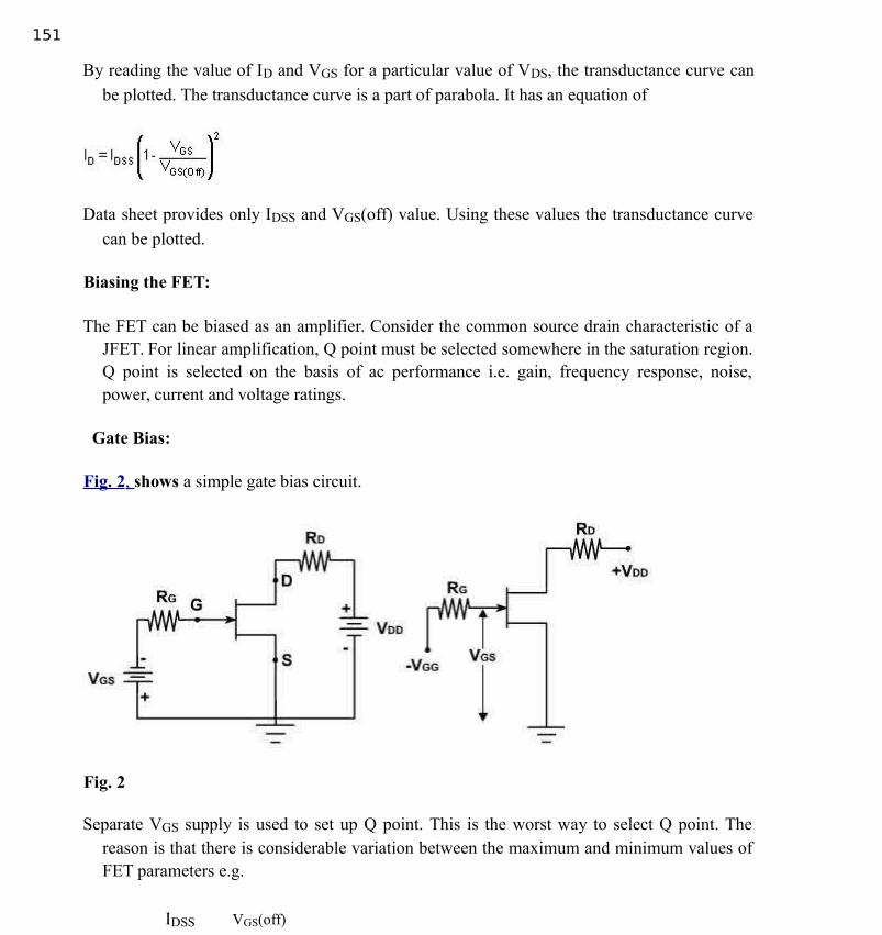
151
By reading the value of ID and VGS for a particular value of VDS, the transductance curve can
be plotted. The transductance curve is a part of parabola. It has an equation of
Data sheet provides only IDSS and VGS(off) value. Using these values the transductance curve
can be plotted.
Biasing the FET:
The FET can be biased as an amplifier. Consider the common source drain characteristic of aJFET. For linear amplification, Q point must be selected somewhere in the saturation region.Q point is selected on the basis of ac performance i.e. gain, frequency response, noise,power, current and voltage ratings.
Gate Bias:
Fig. 2 , shows a simple gate bias circuit.
Fig. 2
Separate VGS supply is used to set up Q point. This is the worst way to select Q point. Thereason is that there is considerable variation between the maximum and minimum values ofFET parameters e.g.
IDSS VGS(off)
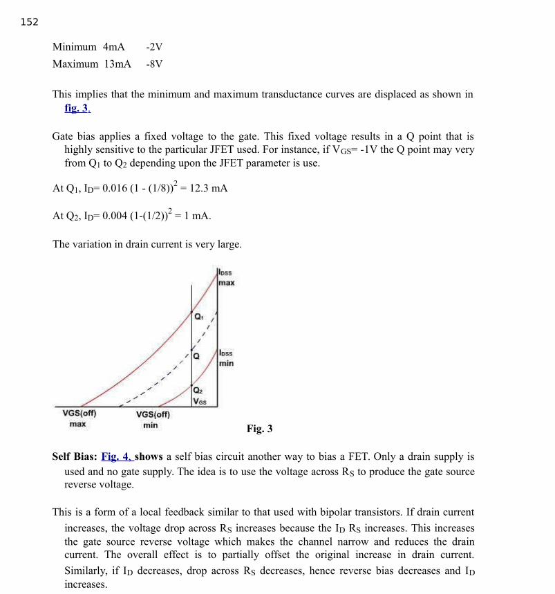
152
Minimum 4mA -2V
Maximum 13mA -8V
This implies that the minimum and maximum transductance curves are displaced as shown infig. 3 .
Gate bias applies a fixed voltage to the gate. This fixed voltage results in a Q point that ishighly sensitive to the particular JFET used. For instance, if VGS= -1V the Q point may veryfrom Q1 to Q2 depending upon the JFET parameter is use.
At Q1, ID= 0.016 (1 - (1/8))2 = 12.3 mA
At Q2, ID= 0.004 (1-(1/2))2 = 1 mA.
The variation in drain current is very large.
Fig. 3
Self Bias: Fig. 4 , shows a self bias circuit another way to bias a FET. Only a drain supply isused and no gate supply. The idea is to use the voltage across RS to produce the gate sourcereverse voltage.
This is a form of a local feedback similar to that used with bipolar transistors. If drain current
increases, the voltage drop across RS increases because the ID RS increases. This increasesthe gate source reverse voltage which makes the channel narrow and reduces the draincurrent. The overall effect is to partially offset the original increase in drain current.
Similarly, if ID decreases, drop across RS decreases, hence reverse bias decreases and ID
increases.

153
Fig. 4
Since the gate source junction is reverse biased, negligible gate current flows through RG and
so the gate voltage with respect to ground is zero.
VG= 0;
The source to ground voltage equals the product of the drain current and the source resistance.
VS= ID R S.
The gate source voltage is the difference between the gate voltage and the source voltage.
VGS = VG ? VS = 0 ? IDRS
VGS = -ID RS.
This means that the gate source voltage equals the negative of the voltage across the sourceresistor. The greater the drain current, the more negative the gate source voltage becomes.
Rearranging the equation:
ID = -VGS / RS
The graph of this equation is called self base line a shown in Fig. 5 .

154
Fig. 5
The operating point on transductance curve is the intersection of self bias line andtransductance curve. The slope of the line is (-1 / RS). If the source resistance is very large (-
1 / RS is small) then Q-point is far down the transductance curve and the drain current is
small. When RS is small, the Q point is far up the transductance curve and the drain current
is large. In between there is an optimum value of RS that sets up a Q point near the middle ofthe transductance curve.
The transductance curve varies widely for FET (because of variation in IDSS and VGS(off)) asshown in fig. 6 . The actual curve may be in between there extremes. A and B are the
optimum points for the two extreme curves. To find the optimum resistance RS, so that Q-point is correct for all the curves, A and B points are joined such that it passes throughorigin.
The slope of this line gives the resistance value RS( VGS = -ID RS). The current IQ is such that
IA > IQ > IB. Here A, Q and B all points are in straight line.

155
Fig. 6
Consider the case where a line drawn to pass between points A and B does not pass through theorigin. The equation VGS = - ID RS is not valid. The equation of this line is VGS = VGG ? ID
RS.
Such a bias relationship may be obtained by adding a fixed bias to the gate in addition to thesource self bias as shown in fig. 7 .
Fig. 7
In this circuit.
VGG = RS IG + VGS + ID RS

156
Since RS IG = 0;
VGG = VGS + ID RS
or VGS = VGG? ID RS
Voltage Divider Bias :
The biasing circuit based on single power supply is shown in fig. 1 . This is similar to the voltage divider bias used with a bipolar transistor.
Fig. 1
The Thevenin voltage VTH applied to the gate is
The Thevenin resistance is given as
The gate current is assumed to be negligible. VTH is the dc voltage from gate to ground.

157
The drain current ID is given by
and the dc voltage from the drain to ground is VD = VDD ? ID RD.
If VTH is large enough to swamp out VGS the drain current is approximately constant for any
JFET as shown in fig. 2 .
Fig. 2
There is a problem in JFET. In a BJT, VBE is approximately 0.7V, with only minor variationsfrom one transistor to other. In a FET, VGS can vary several volts from one JFET to another.It is therefore, difficult to make VTH large enough to swamp out VGS. For this reason,voltage divider bias is less effective with, FET than BJT. Therefore, VGS is not negligible.The current increases slightly from Q2 to Q1. However, voltage divider bias maintains IDnearly constant.
Consider a voltage divider bias circuit shown in fig. 3 .

158
Difference in ID (min) and ID (max) is less
VD (max) = 30 ? 2.13 * 4.7 = 20 V
VD (min) = 30 ? 2.67 * 4.7 = 17.5 V Fig. 3
Current Source Bias:
This is another way to produce solid Q point. The aim is to produce a drain current that isindependent of VGS. Voltage divider bias and self bias attempt to do this by swamping out ofvariations in VGS.
Using two power supplies:
The current source bias can be used to make ID constant fig. 4 .
Fig. 4

159
The bipolar transistor is emitter biased; its collector current is given by
IC = (VEE ? VBE ) / RE.
Because the bipolar transistor acts like a current source, it forces the drain current to equal thebipolar collector current.
ID = IC
Since IC is constant, both Q points have the same value of drain current. The current source
effectively wipes out the influence of VGS. Although VGS is different for each Q point, it nolonger influences the value of drain current.
Using One power supply:
When only a positive supply is available, the circuit shown in fig. 5 , can be used to set up aconstant drain current.
In this case, the bipolar transistor is voltage divider biased. Assuming a stiff voltage divider,the emitter and collector currents are constant for all bipolar transistors. This forces the FETdrain current equal the bipolar collector current.

Fig. 5

160
Transductance: The transductance of a FET is defined as
Because the changes in ID and VGS are equivalent to ac current and voltage. This equation can
be written as
The unit of gm is mho or siemems.
Typical value of gm is 2000 m A / V.
Fig. 6
The value of gm can be obtained from the transductance curve as shown in fig. 6 .
If A and B points are considered, than a change in VGS produces a change in ID. The ratio of ID
and VGS is the value of gm between A and B points. If C and D points are considered, thensame change in VGS produces more change in ID. Therefore, gm value is higher. In anutshell, gm tells us how much control gate voltage has over drain current. Higher the valueof gm, the more effective is gate voltage in controlling gate current. The second parameter rdis the drain resistance.

161
FET a amplifier
Similar to Bipolar junction transistor. JFET can also be used as an amplifier. The ac equivalent circuit of a JFET is shown in fig. 1 .
Fig. 1
The resistance between the gate and the source RGS is very high. The drain of a JFET acts like
a current source with a value of gm Vgs. This model is applicable at low frequencies.
From the ac equivalent model
The amplification factor µ for FET is defined as
When VGS = 0, gm has its maximum value. The maximum value is designated as gmo. Again
consider the equation,

162
As VGS increases, gm decreases linearly.
Measuring IDSS and gm, VGS(off) can be determined
FET as Amplifier:
Fig. 2 , shows a common source amplifier.

163
Fig. 2
When a small ac signal is coupled into the gate it produces variations in gate source voltage.This produces a sinusoidal drain current. Since an ac current flows through the drain resistor.An amplified ac voltage is obtained at the output. An increase in gate source voltageproduces more drain current, which means that the drain voltage is decreasing. Since thepositive half cycle of input voltage produces the negative half cycle of output voltage, weget phase inversion in a CS amplifier.
The ac equivalent circuit is shown in fig. 3 .
Fig. 3
The ac output voltage is
vout = - gm v gS RD
Negative sign means phase inversion. Because the ac source is directly connected between thegate source terminals therefore ac input voltage equals
Vin = Vgs
The voltage gain is given by

The further simplified model of the amplifieris shown in fig. 4 .

164
Fig. 4
Zin is the input impedance. At low frequencies, this is parallel combination of R1|| R2|| RGS.Since RGS is very large, it is parallel combination of R1 & R2. A Vin is output voltage and RDis the output impedance.
Because of nonlinear transductance curve, a JFET distorts large signals, as shown in fig. 5 .
Given a sinusoidal input voltage, we get a non-sinusoidal output current in which positive halfcycle is elongated and negative cycle is compressed. This type of distortion is called Squarelaw distortion because the transductance curve is parabolic.
Fig. 5 Fig. 6
This distortion is undesirable for an amplifier. One way to minimize this is to keep the signalsmall. In that case a part of the curve is used and operation is approximately linear. Some

165
times swamping resistor is used to minimize distortion and gain constant. Now the source is no longer ac ground as shown in fig. 6 .
The drain current through rS produces an ac voltage between the source and ground. If rS islarge enough the local feedback can swamp out the non-linearity of the curve. Then the
voltage gain approaches an ideal value of RD / rS.
Since RGS approaches infinity therefore, all the drain current flows through rS producing a
voltage drop of gm VgS rS. The ac equivalent circuit is shown in fig. 7 .
Fig. 7
The voltage gain reduces but voltage gain is less effective by change in gm. rS must be greater
than 1 / gm only then

166
JFET Applications
Example-1:
Determine gm for an n-channel JFET with characteristic curve shown in fig. 1 .
Fig. 1
Solution:
We select an operating region which is approximately in the middle of the curves; that is,
between vGS = -0.8 V and vGS = -1.2 V; iD = 8.5mA and iD = 5.5 mA. Therefore, thetransductance of the JFET is given by
Design of JFET amplifier:
To design a JFET amplifier, the Q point for the dc bias current can be determined graphically.
The dc bias current at the Q point should lie between 30% and 70% of IDSS. This locates theQ point in the linear region of the characteristic curves.
The relationship between iD and vGS can be plotted on a dimensionless graph (i.e., a
normalized curve) as shown in fig. 2 .
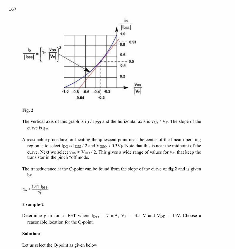
167
Fig. 2
The vertical axis of this graph is iD / IDSS and the horizontal axis is vGS / VP. The slope of the
curve is gm.
A reasonable procedure for locating the quiescent point near the center of the linear operatingregion is to select IDQ ≈ IDSS / 2 and VGSQ ≈ 0.3VP. Note that this is near the midpoint of thecurve. Next we select vDS ≈ VDD / 2. This gives a wide range of values for vds that keep thetransistor in the pinch ?off mode.
The transductance at the Q-point can be found from the slope of the curve of fig.2 and is givenby
Example-2
Determine g m for a JFET where IDSS = 7 mA, VP = -3.5 V and VDD = 15V. Choose a
reasonable location for the Q-point.
Solution:
Let us select the Q-point as given below:

168
The transconductance, gm, is found from the slope of the curve at the point iD / IDSS = 0.5 and
vGS / VP =0.3. Hence,
JEFT as Analog Switch:
JFET can be used as an analog switch as shown in fig. 3 . It is the major application of a JFET.The idea is to use two points on the load line: cut off and saturation. When JFET is cut off, itis like an open switch. When it is saturated, it is like a closed switch.
Fig. 3 Fig. 4
When VGS =0, the JFET is saturated and operates at the upper end of the load line. When VGS
is equal to or more negative than VGS(off) , it is cut off and operates at lower end of the loadline (open and closed switch).This is shown in fig. 4 .
Only these two points are used for operation when used as a switch. The JFET is normallysaturated well below the knee of the drain curve. For this reason the drain current is much
smaller than IDSS .

FET as a Shunt Switch:

169
FET can be used as a shunt switch as shown in fig. 5 . When Vcont=0, the JFT is saturated and
the switch is closed When Vcont is more negative FET is like an open switch. The equivalentcircuit is also shown in fig. 5 .
Fig. 5
FET as a series switch:
JFET can also be used as series switch as shown in fig. 6 . When control is zero, the FET is aclosed switch. When Vcon= negative, the FET is an open switch. It is better than shuntswitch.
Fig. 6
Multiplexing:
One of the important application of FET is in analog multiplexer. Analog multiplexer is acircuit that selects one of the output lines as shown in fig. 7 . When control voltages are morenegative all switches are open and output is zero. When any control voltage becomes zerothe input is transmitted to the output.
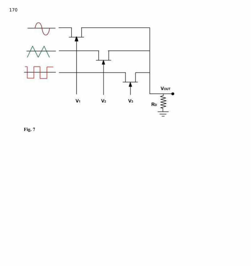
170
Fig. 7