Analog Circuits and Systems - NPTELnptel.ac.in/courses/117108107/Lecture 16.pdf · 741 is a general...
38
Analog Circuits and Systems Prof. K Radhakrishna Rao Lecture 16: Amplifiers 1
Transcript of Analog Circuits and Systems - NPTELnptel.ac.in/courses/117108107/Lecture 16.pdf · 741 is a general...

Analog Circuits and Systems Prof. K Radhakrishna Rao
Lecture 16: Amplifiers
1
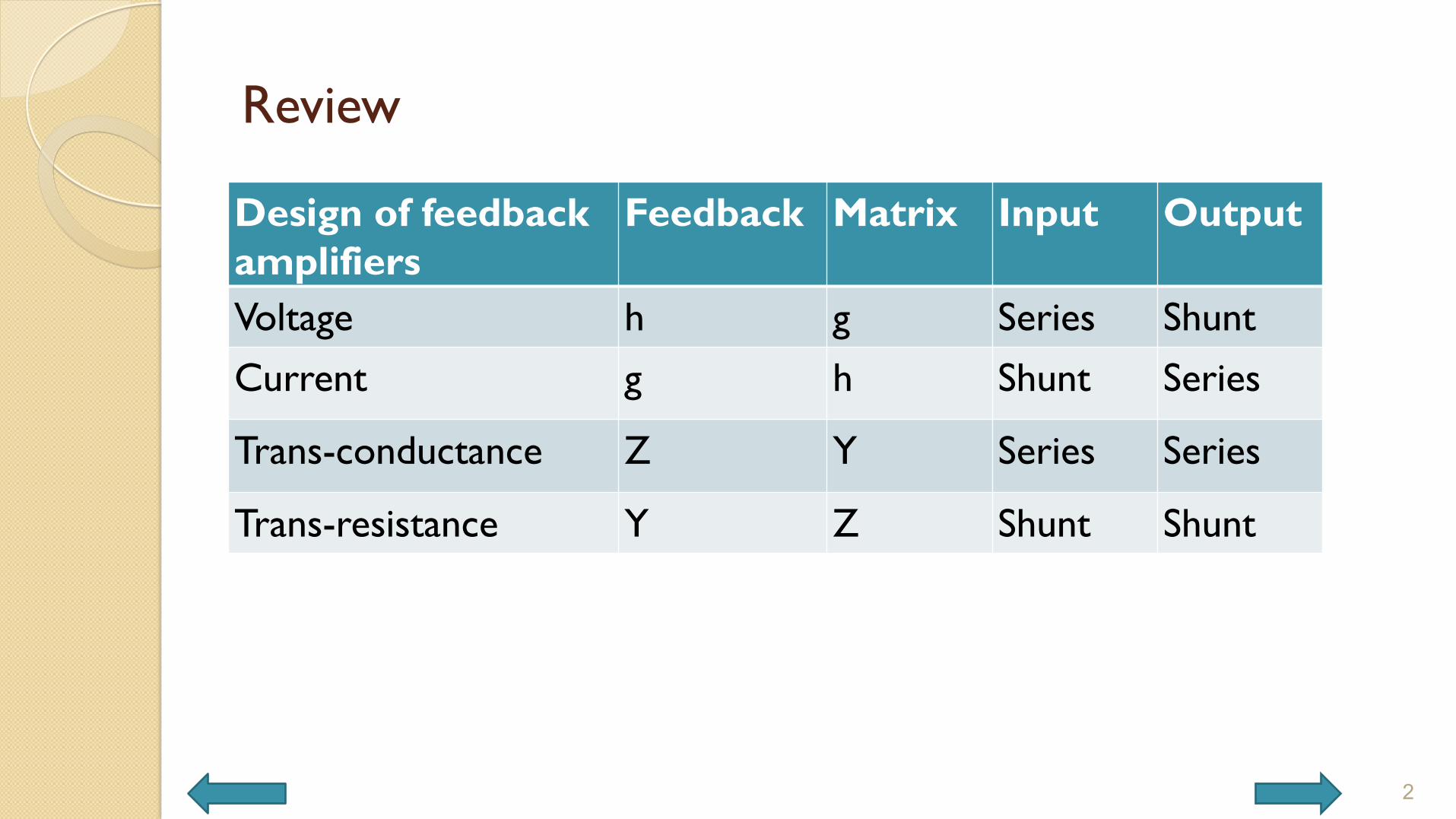
Review
2
Design of feedback amplifiers
Feedback Matrix Input Output
Voltage h g Series Shunt Current g h Shunt Series
Trans-conductance Z Y Series Series
Trans-resistance Y Z Shunt Shunt

Voltage Amplifier (VCVS)
� Ideal VCVS
� Non-ideal amplifier
3
i i
o of
I V0 0=
V Ig 0⎡ ⎤ ⎡ ⎤⎡ ⎤⎢ ⎥ ⎢ ⎥⎢ ⎥
⎣ ⎦⎣ ⎦ ⎣ ⎦
i ia i
o fa oa o
V h 0 I=
I h h V⎡ ⎤ ⎡ ⎤ ⎡ ⎤⎢ ⎥ ⎢ ⎥ ⎢ ⎥⎣ ⎦ ⎣ ⎦ ⎣ ⎦
iaia ia oa fa
oa oa
AR1h R ; h ; hR R
= = = −

Feedback arrangement to obtain near Ideal VCVS
4

Feedback Passive Network and its h-parameter
5
fp 1
o 1 2
V R=V R +R
11 2
1 2
1
1 2 1 2
RR RR R
R 1R R R R
⎡ ⎤⎢ ⎥+⎢ ⎥⎢ ⎥−⎢ ⎥+ +⎣ ⎦

Composite Network
6
( ) 1ia 1 2 S
1 2
ia 1
oa 1 2 1 2 oa L
1L L
1 2
RR R R RR R
AR R 1 1 1R R R R R R R
ARg ; g 1R R
⎡ ⎤⎛ ⎞+ +⎢ ⎥⎜ ⎟+⎝ ⎠⎢ ⎥
⎢ ⎥⎛ ⎞ ⎛ ⎞⎢ ⎥− + + +⎜ ⎟ ⎜ ⎟⎢ ⎥+ +⎝ ⎠ ⎝ ⎠⎣ ⎦
−+
; ?

g-matrix
7
oa oa 2
1 2 L 1 oa
ia ia
1 2 s 2oa
ia ia 12
1
R R R1 1R R R R R
R A AR
R R R R1 1 RR R RR1
R A
⎡ ⎤⎛ ⎞⎛ ⎞+ + +⎢ ⎥⎜ ⎟⎜ ⎟+⎝ ⎠⎝ ⎠⎢ ⎥−⎢ ⎥
⎢ ⎥⎛ ⎞⎛ ⎞⎢ ⎥+ + +⎜ ⎟⎜ ⎟⎢ ⎥
⎝ ⎠⎝ ⎠⎢ ⎥+⎢ ⎥⎣ ⎦

Macro-model of VCVS
8

VCVS
9

Example 1
� 741 is a general purpose Op Amp with a DC voltage gain of 106 (120dB), input resistance of (Ria) 1MW and output resistance of Roa=100W, RS=10k, RL=10k. Let us consider the design of a non-inverting amplifier of gain 100.
10
2
1
1 2 1
2 1
R1+ =100R
R +R =100RR =99R
This requires,

Example 1 (contd.,)
11
( )
oa oa 2
1 2 L 1i
ia
oa
1 2 L 106 6
R R R1 1R R R R
gR A
R1001 100R R R
S 10 S10 10
−
⎛ ⎞⎛ ⎞+ + +⎜ ⎟⎜ ⎟+⎝ ⎠⎝ ⎠=
⎛ ⎞+ +⎜ ⎟+⎝ ⎠= =
Substituting the values
which can be approximated to zero.

Example 1 (contd.,)
12
1 2 s 2oa
ia ia 1o
26 6 2
6
-10oar 6 6
ia
R R R R1 R 1R R R
gA
R 1001 100 10099 10 10 1 10
10R 100g - 10AR 10 10
which can be approximated to zero.
−
⎛ ⎞ ⎛ ⎞+ + +⎜ ⎟ ⎜ ⎟
⎝ ⎠⎝ ⎠=
⎛ ⎞+ + ×⎜ ⎟×⎝ ⎠= × Ω
= − = = −×
;
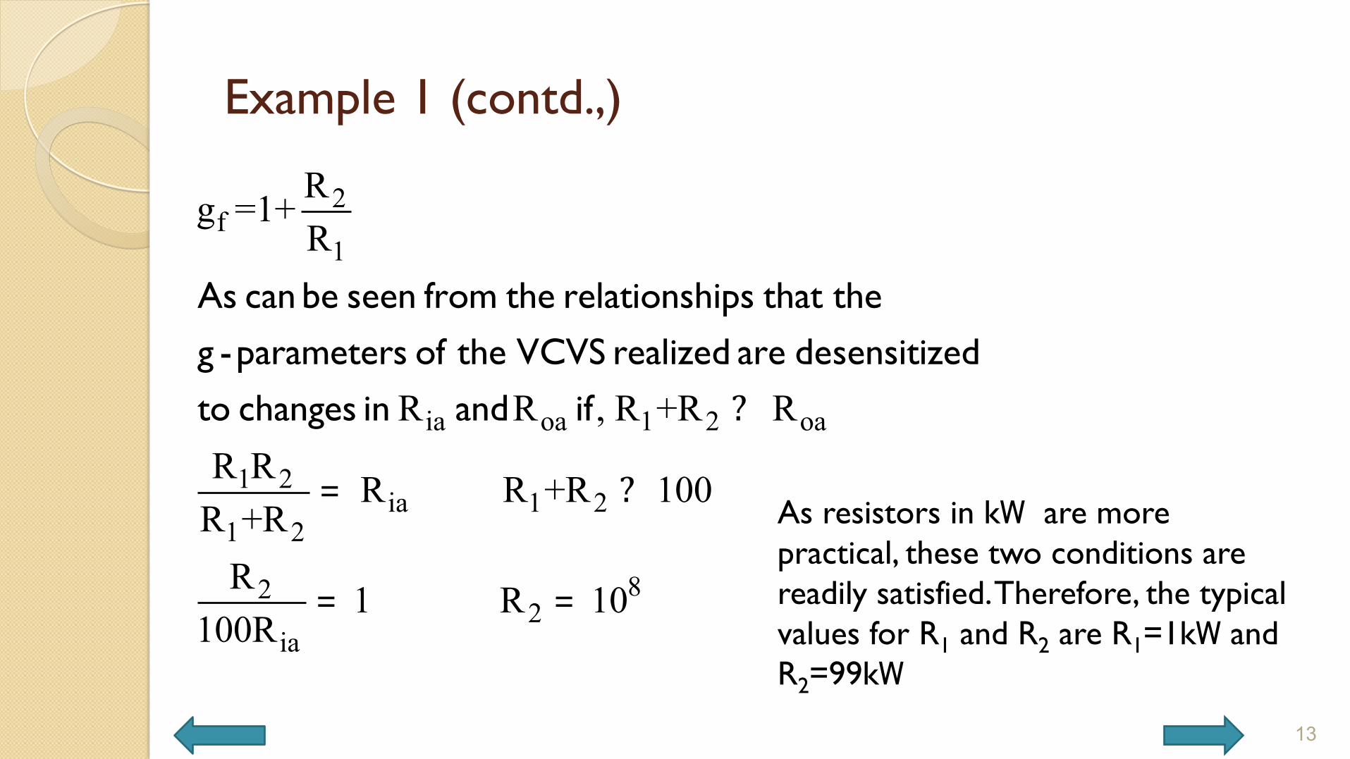
Example 1 (contd.,)
13
2f
1
ia oa 1 2 oa
1 2ia 1 2
1 2
822
ia
Rg =1+R
R R , R +R RR R R R +R 100
R +RR 1 R 10
100R
?
= ?
= =
As can be seen from the relationships that the g -parameters of the VCVS realized are desensitized to changes in and if
As resistors in kW are more practical, these two conditions are readily satisfied. Therefore, the typical values for R1 and R2 are R1=1kW and R2=99kW

Example 1 (contd.,)
� Note that the gain is sensitive to variations in the parameters of the feedback circuit
14

VCCS – Trans-conductance Amplifier
� High frequency filters � Analog multiplexers and sample and hold circuits � Modulators and mixers � TI 3080 and OPA 860
15

Ideal VCCS
16
i i
o om
I V0 0=
I Vg 0⎡ ⎤ ⎡ ⎤⎡ ⎤⎢ ⎥ ⎢ ⎥⎢ ⎥
⎣ ⎦⎣ ⎦ ⎣ ⎦

Feedback around non-ideal amplifier
17
To convert it into a VCCS
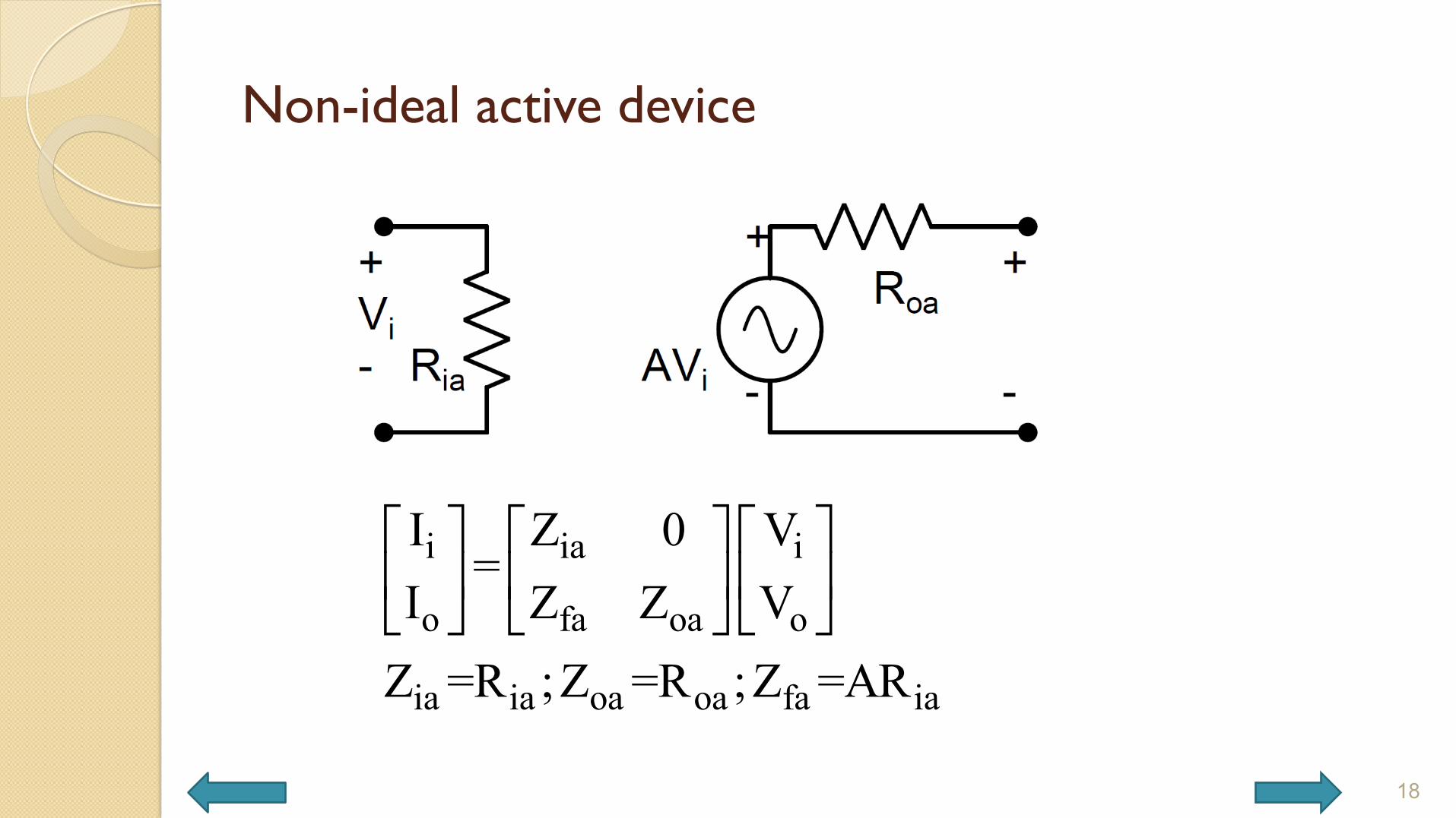
Non-ideal active device
18
i ia i
o fa oa o
ia ia oa oa fa ia
I Z 0 V=
I Z Z VZ =R ;Z =R ;Z =AR
⎡ ⎤ ⎡ ⎤ ⎡ ⎤⎢ ⎥ ⎢ ⎥ ⎢ ⎥⎣ ⎦ ⎣ ⎦ ⎣ ⎦

Macro-model of VCCS
19

Z-matrix and Y-matrix
20
( )( )
( )
( )
( )
( )
ia f S f
ia f oa f L
oa f L f
ia fia f Sia f
oa f L f
ia f ia f
ia f S
f ia f
R +R +R -RZ-matrix of composite network
AR -R R +R +R
R +R +R R
Y-matrix of VCCS where AR RR +R +R-AR +R
R +R +R R0 0
AR R AR R1
R +R +R1R AR R
⎡ ⎤⎢ ⎥⎣ ⎦
⎡ ⎤⎢ ⎥Δ Δ⎢ ⎥ Δ⎢ ⎥⎢ ⎥⎣ Δ Δ ⎦⎡ ⎤⎢ ⎥⎢ ⎥≈ ⎢ ⎥ −⎢ ⎥−⎢ ⎥⎣ ⎦
;
;
( )( )( )
f
f iaL L
ia f S oa f L
0R
R -ARg ; g 1
R +R +R R +R +R
⎡ ⎤⎢ ⎥⎢ ⎥⎢ ⎥⎣ ⎦
; ?

VCCS
21

Example 2a
� Design a voltage controlled current source with a trans-conductance of -1 mS for a source with Rs = 10 kW and with a load of 1 kW using 741 Op Amp.
� 741 is a general purpose Voltage Op Amp with a DC voltage gain of 105 (100dB), input resistance of (Ria) 1MW and output resistance of Roa=100W.
� Rf=1kW
22
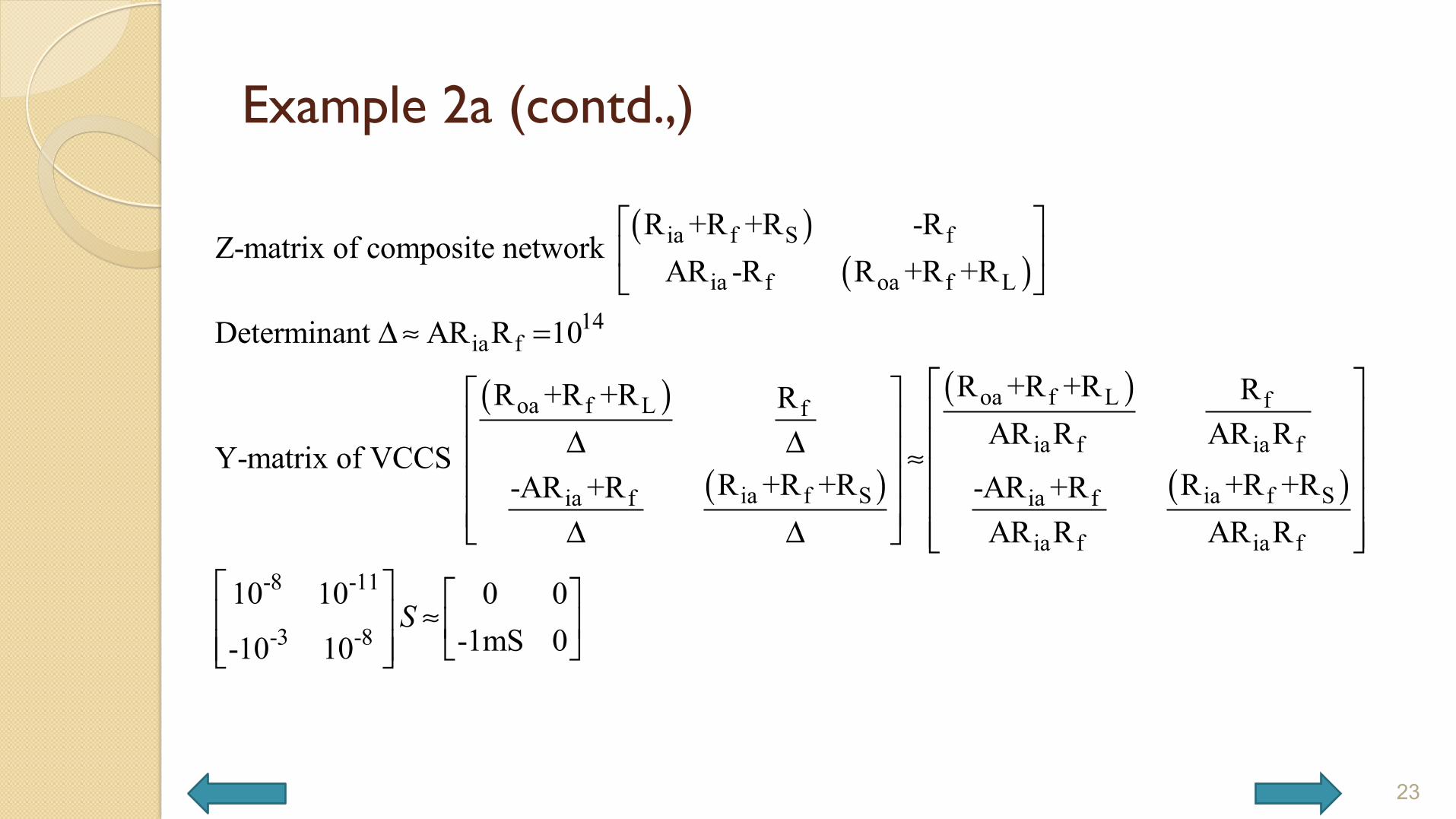
Example 2a (contd.,)
23
( )( )
( )
( )
( )
( )
ia f S f
ia f oa f L
14ia f
oa f L foa f L fia f ia f
ia f S ia f Sia f ia f
ia f i
R +R +R -RZ-matrix of composite network
AR -R R +R +R
Determinant AR R 10
R +R +R RR +R +R RAR R AR R
Y-matrix of VCCS R +R +R R +R +R-AR +R -AR +R
AR R AR
⎡ ⎤⎢ ⎥⎣ ⎦
Δ≈ =
⎡ ⎤⎢ ⎥Δ Δ⎢ ⎥ ≈⎢ ⎥⎢ ⎥⎣ Δ Δ ⎦ a f
-8 -11
-3 -8
R
10 10 0 0-1mS 0-10 10
⎡ ⎤⎢ ⎥⎢ ⎥⎢ ⎥⎢ ⎥⎢ ⎥⎣ ⎦
⎡ ⎤ ⎡ ⎤≈⎢ ⎥ ⎢ ⎥⎣ ⎦⎢ ⎥⎣ ⎦
S
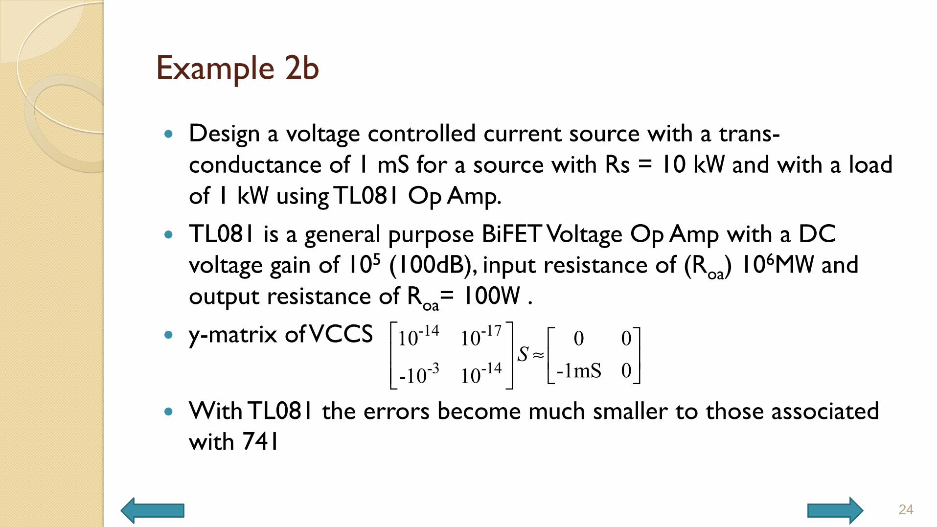
Example 2b
� Design a voltage controlled current source with a trans-conductance of 1 mS for a source with Rs = 10 kW and with a load of 1 kW using TL081 Op Amp.
� TL081 is a general purpose BiFET Voltage Op Amp with a DC voltage gain of 105 (100dB), input resistance of (Roa) 106MW and output resistance of Roa= 100W .
� y-matrix of VCCS
� With TL081 the errors become much smaller to those associated with 741
24
-14 -17
-3 -14
10 10 0 0-1mS 0-10 10
⎡ ⎤ ⎡ ⎤≈⎢ ⎥ ⎢ ⎥⎣ ⎦⎢ ⎥⎣ ⎦
S

CCCS: Current Amplifier
� As supply voltages of Op Amps are getting reduced to keep up with present day demand for lower supply voltages current amplifiers provide a better option to voltage amplifier
� Operational current amplifiers are not commercially popular
25
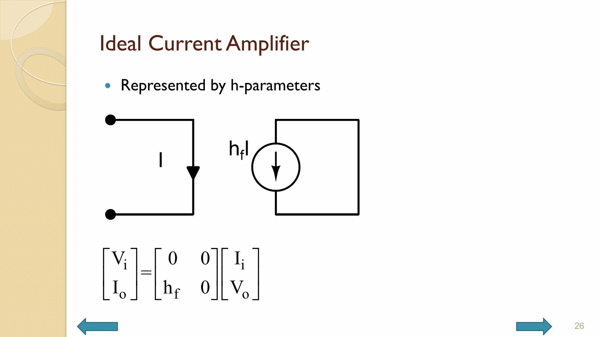
Ideal Current Amplifier
� Represented by h-parameters
26
i i
o of
V I0 0=
I Vh 0⎡ ⎤ ⎡ ⎤⎡ ⎤⎢ ⎥ ⎢ ⎥⎢ ⎥
⎣ ⎦⎣ ⎦ ⎣ ⎦

Ideal Current Amplifier (contd.,)
� Input impedance can be brought down (CC) by shunt arrangement at the input and output impedance can be increased (CS) by series arrangement at the output.
27
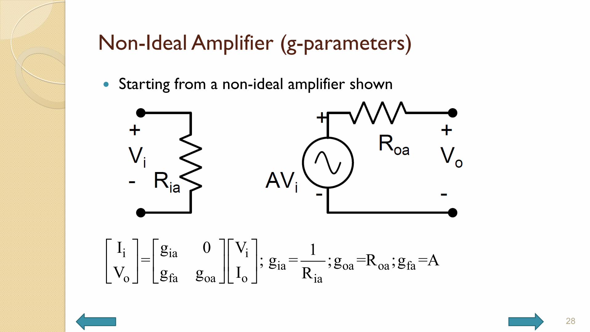
Non-Ideal Amplifier (g-parameters)
� Starting from a non-ideal amplifier shown
28
i ia iia oa oa fa
o fa oa o ia
I g 0 V 1= ; g = ;g =R ;g =AV g g I R⎡ ⎤ ⎡ ⎤ ⎡ ⎤⎢ ⎥ ⎢ ⎥ ⎢ ⎥⎣ ⎦ ⎣ ⎦ ⎣ ⎦
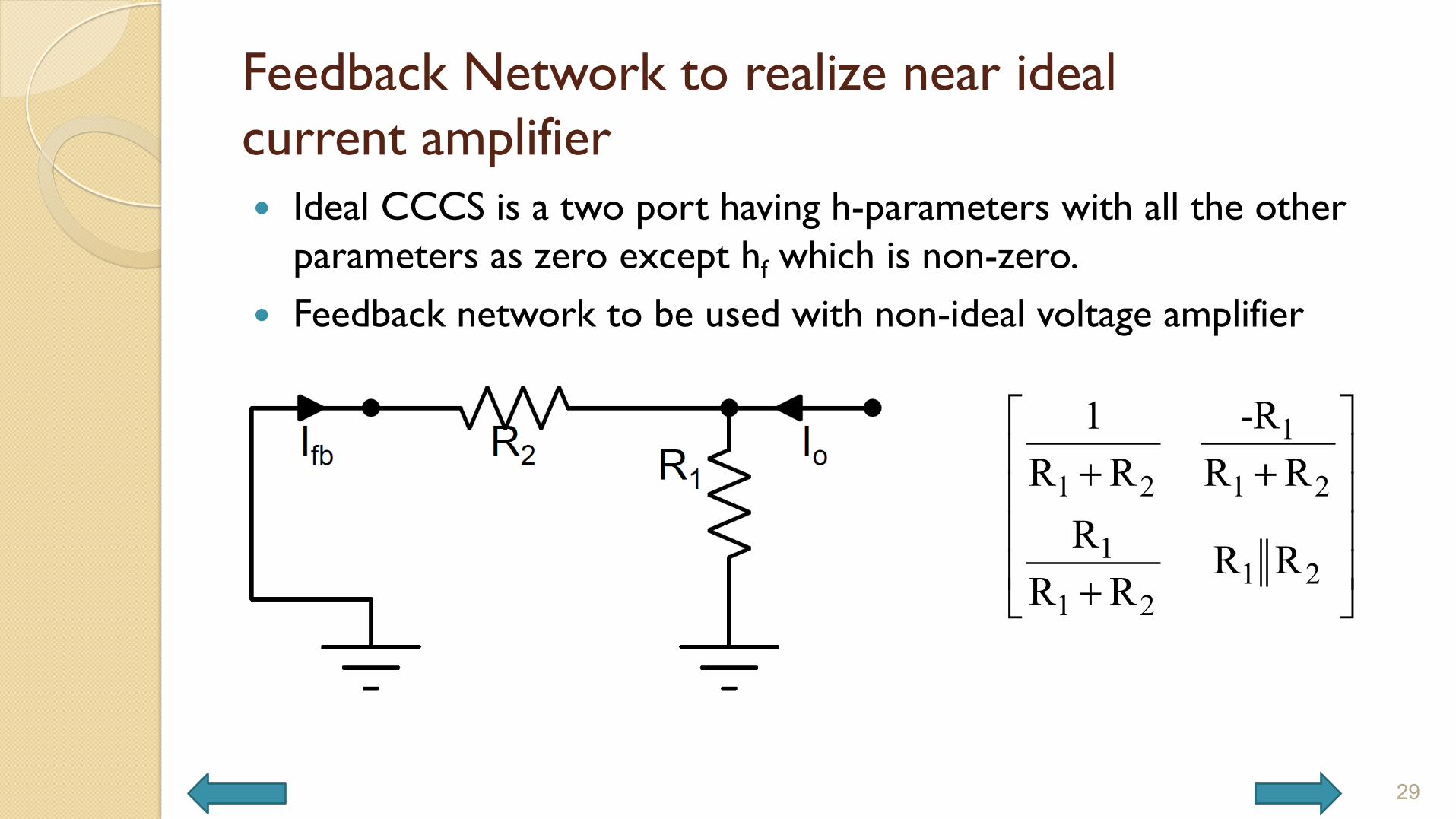
Feedback Network to realize near ideal current amplifier � Ideal CCCS is a two port having h-parameters with all the other
parameters as zero except hf which is non-zero. � Feedback network to be used with non-ideal voltage amplifier
29
1
1 2 1 2
11 2
1 2
-R1R R R RR R R
R R
⎡ ⎤⎢ ⎥+ +⎢ ⎥⎢ ⎥⎢ ⎥+⎣ ⎦

Macro-model of CCCS
30

Ideal Current Amplifier (contd.,)
� Inverting to modify these � Determinant
� h-matrix of CCCS
31
1
1 2
ARΔR +R
;
( )1
1 2 oa L 1 2
2
1ia 1 2 S
RR R +R ||R R +R 0 0
R1 01 1 1+ RR R +R RA
⎡ ⎤⎢ ⎥
⎡ ⎤⎢ ⎥⎢ ⎥Δ Δ⎢ ⎥ ≈ ⎛ ⎞⎢ ⎥⎢ ⎥ − +⎜ ⎟⎢ ⎥+⎢ ⎥ ⎝ ⎠⎣ ⎦
⎢ ⎥−⎢ ⎥⎣ Δ Δ ⎦

Ideal Current Amplifier (contd.,)
� Composite network converting h-matrix to g-matrix � Composite g-matrix
32
( )
1
ia 1 2 S 1 2
11 2 oa L
1 2
R1 1 1+R R +R R R +R
RA+ R R +R ||RR +R
⎡ ⎤+ −⎢ ⎥⎢ ⎥⎢ ⎥⎢ ⎥⎣ ⎦

CCCS
33

Example 3
� Design a current amplifier with a current gain of -10 for a source with Rs = 10 kW and with a load of 1 kW using 741 Op Amp.
� 741 is a general purpose Voltage Op Amp with a DC voltage gain of 105 (100dB), input resistance of (Ria) 1MW and output resistance of Roa=100W.
34
2 54 5
44
500 15 10 10 0 0
10 1010 010 2 1010 2 10
− −
−−
⎡ ⎤ ⎡ ⎤× ⎡ ⎤⎢ ⎥ = =⎢ ⎥ ⎢ ⎥⎢ ⎥ −⎣ ⎦⎢ ⎥− ×⎣ ⎦⎢ ⎥− ×⎣ ⎦

CCCS – Current Amplifier of gain=-10
35

Conclusion
Feedback Final Parameter Amplifier [h]-1 g VCVS (Voltage) [g]-1 h CCCS (Current) [y]-1 Z CCVS (Trans-impedance) [z]-1 Y VCCS (Trans-admittance)
36

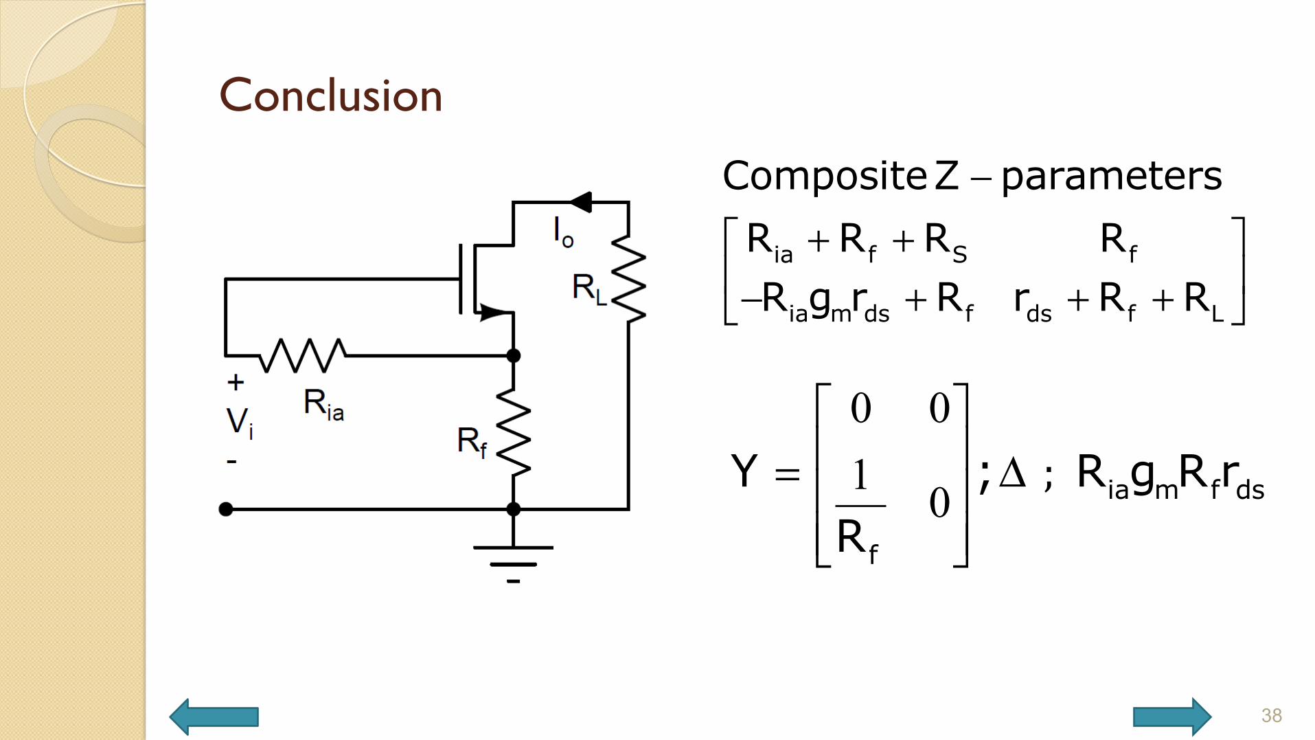
Conclusion
� Design of Trans-impedance amplifier using a transistor.
37
−+ −⎡ ⎤
⎢ ⎥− + +⎣ ⎦s f f
m f ds L f
Composite Y parametersg g gg g g g g
1
1
0 00
+ +⎡ ⎤⎢ ⎥⎢ ⎥=⎢ ⎥+−⎢ ⎥⎣ ⎦⎡ ⎤
= Δ⎢ ⎥−⎣ ⎦? ;
ds L f
m f m
s f
f m f
m m ff
g g gg g g
Zg g
g g g
;g g; g gR
Conclusion
38
−+ +⎡ ⎤
⎢ ⎥− + + +⎣ ⎦ia f S f
ia m ds f ds f L
CompositeZ parametersR R R RR g r R r R R
0 01 0
⎡ ⎤⎢ ⎥= Δ⎢ ⎥⎢ ⎥⎣ ⎦
; ia m f ds
f
Y ; R g R rR