AN4943 Application note - STMicroelectronics...Chrom-ART Accelerator™ (DMA2D) application use case...
22
October 2017 DocID029937 Rev 2 1/22 1 AN4943 Application note Using the Chrom-ART Accelerator™ to refresh an LCD-TFT display on STM32L496xx/L4A6xx/L4Rxxx/L4Sxxx microcontrollers Introduction The purpose of this application note is to highlight how to refresh an LCD-TFT display via the FSMC interface using the Chrom-ART Accelerator™ on STM32L496xx/L4A6xx/L4Rxxx/L4Sxxx microcontrollers. The STM32L496xx/L4A6xx/L4Rxxx/L4Sxxx microcontrollers implement a Chrom-Art Accelerator™ (DMA2D) that is a specialized DMA dedicated to image manipulation. It can perform the following operations: • Filling a part or the whole of a destination image with a specific color • Copying a part or the whole of a source image into a part or the whole of a destination image with a pixel format conversion • Blending a part and/or two complete source images with a different pixel format and copying the result into a part or the whole of a destination image with a different color format. On the STM32L496xx/L4A6xx/L4Rxxx/L4Sxxx microcontrollers, the flexible static memory controller (FSMC) is used to access the LCD-TFT display through a parallel interface. This application note explains on: • How to connect the LCD-TFT display to the FSMC interface • How to configure the DMA2D for the LCD-TFT display refresh • How to use the DMA2D byte reordering features to directly drive Intel 8080 displays. To fully benefit from this application note, the user should be familiar with the STM32 Chrom-ART Accelerator™ (DMA2D) as described in the STM32L4x6 advanced Arm ® - based 32-bit MCUs reference manual (RM0351) and the STM32L4Rxxx/L4Sxxx advanced Arm ® -based 32-bit MCUs reference manual (RM0432) available from the STMicroelectronics website www.st.com. Table 1. Applicable products Type Product lines and part numbers Microcontrollers STM32L496AE, STM32L496AG, STM32L496QE, STM32L496QG, STM32L496RE, STM32L496RG, STM32L496VE, STM32L496VG, STM32L496ZE, STM32L496ZG STM32L4A6AG, STM32L4A6QG, STM32L4A6RG, STM32L4A6VG, STM32L4A6ZG STM32L4R5/S5 line, STM32L4R7/S7 line, STM32L4R9/S9 line www.st.com
Transcript of AN4943 Application note - STMicroelectronics...Chrom-ART Accelerator™ (DMA2D) application use case...

October 2017 DocID029937 Rev 2 1/22
1
AN4943Application note
Using the Chrom-ART Accelerator™ to refresh an LCD-TFT display on STM32L496xx/L4A6xx/L4Rxxx/L4Sxxx microcontrollers
Introduction
The purpose of this application note is to highlight how to refresh an LCD-TFT display via the FSMC interface using the Chrom-ART Accelerator™ on STM32L496xx/L4A6xx/L4Rxxx/L4Sxxx microcontrollers.
The STM32L496xx/L4A6xx/L4Rxxx/L4Sxxx microcontrollers implement a Chrom-Art Accelerator™ (DMA2D) that is a specialized DMA dedicated to image manipulation.
It can perform the following operations:
• Filling a part or the whole of a destination image with a specific color
• Copying a part or the whole of a source image into a part or the whole of a destination image with a pixel format conversion
• Blending a part and/or two complete source images with a different pixel format and copying the result into a part or the whole of a destination image with a different color format.
On the STM32L496xx/L4A6xx/L4Rxxx/L4Sxxx microcontrollers, the flexible static memory controller (FSMC) is used to access the LCD-TFT display through a parallel interface.
This application note explains on:
• How to connect the LCD-TFT display to the FSMC interface
• How to configure the DMA2D for the LCD-TFT display refresh
• How to use the DMA2D byte reordering features to directly drive Intel 8080 displays.
To fully benefit from this application note, the user should be familiar with the STM32 Chrom-ART Accelerator™ (DMA2D) as described in the STM32L4x6 advanced Arm®-based 32-bit MCUs reference manual (RM0351) and the STM32L4Rxxx/L4Sxxx advanced Arm®-based 32-bit MCUs reference manual (RM0432) available from the STMicroelectronics website www.st.com.
Table 1. Applicable products
Type Product lines and part numbers
Microcontrollers
STM32L496AE, STM32L496AG, STM32L496QE, STM32L496QG, STM32L496RE, STM32L496RG, STM32L496VE, STM32L496VG, STM32L496ZE, STM32L496ZG
STM32L4A6AG, STM32L4A6QG, STM32L4A6RG, STM32L4A6VG, STM32L4A6ZG
STM32L4R5/S5 line, STM32L4R7/S7 line, STM32L4R9/S9 line
www.st.com

Contents AN4943
2/22 DocID029937 Rev 2
Contents
1 Reference documents . . . . . . . . . . . . . . . . . . . . . . . . . . . . . . . . . . . . . . . . 5
2 Chrom-ART Accelerator™ (DMA2D) application use case overview . . 6
3 LCD-TFT display on FSMC . . . . . . . . . . . . . . . . . . . . . . . . . . . . . . . . . . . . 7
3.1 Hardware interface description . . . . . . . . . . . . . . . . . . . . . . . . . . . . . . . . . . 7
3.2 Display Command Set (DCS) software interface . . . . . . . . . . . . . . . . . . . . 8
3.3 Controlling the D/CX signal with STM32L496xx/L4A6xx/ L4Rxxx/L4Sxxx microcontrollers . . . . . . . . . . . . . . . . . . . . . . . . . . . . . . . . 9
4 Chrom-ART Accelerator™ (DMA2D) configuration in STM32CubeL4 11
4.1 LCD partial refresh . . . . . . . . . . . . . . . . . . . . . . . . . . . . . . . . . . . . . . . . . . .11
5 New DMA2D features to support Intel 8080 displays . . . . . . . . . . . . . . 13
5.1 Intel 8080 interface color coding . . . . . . . . . . . . . . . . . . . . . . . . . . . . . . . 13
5.2 DMA2D reordering features . . . . . . . . . . . . . . . . . . . . . . . . . . . . . . . . . . . 16
5.2.1 Red and blue swap . . . . . . . . . . . . . . . . . . . . . . . . . . . . . . . . . . . . . . . . 16
5.2.2 Byte swap . . . . . . . . . . . . . . . . . . . . . . . . . . . . . . . . . . . . . . . . . . . . . . . 16
5.3 DMA2D reordering use case examples . . . . . . . . . . . . . . . . . . . . . . . . . . 17
5.3.1 24bpp/18bpp over 16-bit FSMC data bus interface . . . . . . . . . . . . . . . . 17
5.3.2 24bpp/18bpp over 8-bit FSMC data bus interface . . . . . . . . . . . . . . . . . 18
5.3.3 16bpp over 8-bit FSMC data bus interface . . . . . . . . . . . . . . . . . . . . . . 19
6 Conclusion . . . . . . . . . . . . . . . . . . . . . . . . . . . . . . . . . . . . . . . . . . . . . . . . 20
7 Revision history . . . . . . . . . . . . . . . . . . . . . . . . . . . . . . . . . . . . . . . . . . . 21
DocID029937 Rev 2 3/22
AN4943 List of tables
3
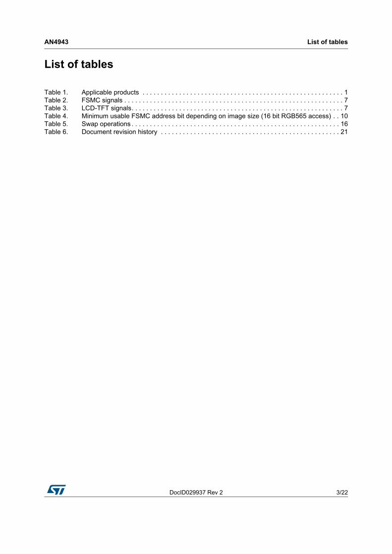
List of tables
Table 1. Applicable products . . . . . . . . . . . . . . . . . . . . . . . . . . . . . . . . . . . . . . . . . . . . . . . . . . . . . . . 1Table 2. FSMC signals . . . . . . . . . . . . . . . . . . . . . . . . . . . . . . . . . . . . . . . . . . . . . . . . . . . . . . . . . . . . 7Table 3. LCD-TFT signals. . . . . . . . . . . . . . . . . . . . . . . . . . . . . . . . . . . . . . . . . . . . . . . . . . . . . . . . . . 7Table 4. Minimum usable FSMC address bit depending on image size (16 bit RGB565 access) . . 10Table 5. Swap operations . . . . . . . . . . . . . . . . . . . . . . . . . . . . . . . . . . . . . . . . . . . . . . . . . . . . . . . . . 16Table 6. Document revision history . . . . . . . . . . . . . . . . . . . . . . . . . . . . . . . . . . . . . . . . . . . . . . . . . 21

List of figures AN4943
4/22 DocID029937 Rev 2
List of figures
Figure 1. Display application typical use case . . . . . . . . . . . . . . . . . . . . . . . . . . . . . . . . . . . . . . . . . . . 6Figure 2. Display bus interface specification . . . . . . . . . . . . . . . . . . . . . . . . . . . . . . . . . . . . . . . . . . . . 8Figure 3. Memory map for LCD-TFT display access . . . . . . . . . . . . . . . . . . . . . . . . . . . . . . . . . . . . . . 9Figure 4. Automatic control of LCD-TFT display data/command by FSMC interface . . . . . . . . . . . . 10Figure 5. 24bpp over 16-bit interface color coding. . . . . . . . . . . . . . . . . . . . . . . . . . . . . . . . . . . . . . . 14Figure 6. 16bpp over 8-bit interface color coding. . . . . . . . . . . . . . . . . . . . . . . . . . . . . . . . . . . . . . . . 15Figure 7. 24bpp over 8-bit interface color coding. . . . . . . . . . . . . . . . . . . . . . . . . . . . . . . . . . . . . . . . 15Figure 8. DMA2D operations to support 24bpp over 16-bit interface. . . . . . . . . . . . . . . . . . . . . . . . . 17Figure 9. DMA2D operations to support 24bpp over 8-bit interface. . . . . . . . . . . . . . . . . . . . . . . . . . 18Figure 10. DMA2D operations to support 16bpp over 8-bit interface. . . . . . . . . . . . . . . . . . . . . . . . . . 19
DocID029937 Rev 2 5/22
AN4943 Reference documents
21
1 Reference documents
The following documents are available on www.st.com.
• STM32L4x6 advanced Arm®-based 32-bit MCUs reference manual (RM0351)
• STM32L4Rxxx/L4Sxxx advanced Arm®-based 32-bit MCUs reference manual (RM0432)
• Discovery kit with STM32L496AG MCU user manual (UM2160)
• Embedded software for the STM32L4 Series (STM32CubeL4)
This application note applies to Arm®-based devices.

Chrom-ART Accelerator™ (DMA2D) application use case overview AN4943
6/22 DocID029937 Rev 2
2 Chrom-ART Accelerator™ (DMA2D) application use case overview
A typical application displaying an image into an LCD-TFT display is divided in 2 steps.
• Step1: creation of the frame buffer content
– The frame buffer is built by composing graphical primitives like icons, pictures and fonts
– This operation is done by the CPU running a graphical library software
– It can be accelerated by a dedicated hardware used with the CPU through the graphical library (Chrom-ART Accelerator™ (DMA2D))
– The more often the frame buffer is updated, the more fluid are the animations
• Step2: display of the frame buffer onto the LCD-TFT display
– The frame buffer is transferred to the display through a dedicated hardware interface
– The transfer can be done using the CPU, the system DMA or using the Chrom-ART Accelerator™ (DMA2D)
In a typical display application example using the STM32L496xx/L4A6xx/L4Rxxx/L4Sxxx microcontrollers, the Flexible Static Memory Controller (FSMC) is used as the hardware interface to the LCD-TFT display, the graphical primitives like pictures, icons or fonts are stored in the external Quad-SPI Flash memory and the frame buffer is stored in the internal SRAM. The transfer of the frame buffer to the LCD-TFT display can also be managed by the Chrom-ART Accelerator™ (DMA2D), hence not using the CPU or the DMA resources.
This is showed in Figure 1: Display application typical use case.
Figure 1. Display application typical use case
MSv44235V2
Frame buffer in internal SRAM
STM32L496xx/L4A6xx/L4Rxxx/L4Sxxx
SRAMDMA2D
FSMC
LCD-TFT display
Quad-SPI Flash
Quad-SPI interface
Graphical primitives in external Quad-SPI Flash memory
Step 1Step 2

DocID029937 Rev 2 7/22
AN4943 LCD-TFT display on FSMC
21
The Chrom-ART Accelerator™ (DMA2D) can update the whole image on the display (full refresh) or only a part of it (partial refresh).
The configuration of the Chrom-ART Accelerator™ (DMA2D) (full or partial refresh) is done by programming specific registers through the high level HAL library function as shown in Section 4: Chrom-ART Accelerator™ (DMA2D) configuration in STM32CubeL4.
3 LCD-TFT display on FSMC
3.1 Hardware interface description
The below signals are used to connect the Flexible Static Memory interface (FSMC) to the LCD-TFT display:
Table 2. FSMC signals
Signal name FSMC I/O Function
A[25:0] O Address bus
D[15:0] I/O Bidirectional data bus
NE[x] O Chip select, x=1..4
NOE O Output enable
NWE O Write enable
Table 3. LCD-TFT signals
Signal name(1)
1. The signal names are provided according the Type B Display Bus Interface (DBI) as described in the MIPI Alliance standard for display bus interface.
LCD-TFT I/O Function
D/CX I Data/command control signal
D[15:0] I/O Bidirectional information signals bus
CSX I Chip select control signal
RDX I Read control signal
WRX I Write control signal
TE O Tearing effect
RESX I Reset
LCD-TFT display on FSMC AN4943
8/22 DocID029937 Rev 2
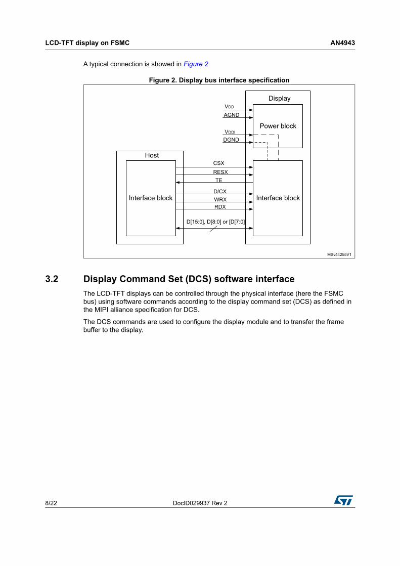
A typical connection is showed in Figure 2
Figure 2. Display bus interface specification
3.2 Display Command Set (DCS) software interface
The LCD-TFT displays can be controlled through the physical interface (here the FSMC bus) using software commands according to the display command set (DCS) as defined in the MIPI alliance specification for DCS.
The DCS commands are used to configure the display module and to transfer the frame buffer to the display.
MSv44255V1
CSX
VDD
RESXTE
VDDI
D[15:0], D[8:0] or [D[7:0]
AGND
DGND
Power block
Interface block
Host
Interface blockD/CXWRXRDX
Display

DocID029937 Rev 2 9/22
AN4943 LCD-TFT display on FSMC
21
3.3 Controlling the D/CX signal with STM32L496xx/L4A6xx/ L4Rxxx/L4Sxxx microcontrollers
The D/CX signal of the DBI protocol is used to distinguish the commands (when D/CX = 0) from the data (when D/CX = 1) transfers.
There are 2 ways to control the 'Data/Command control' (D/CX) signal:
1. By using a dedicated GPIO:
– Setting the 'Data/Command control' signal in "command mode" (setting the GPIO connected to the D/CX signal to '0' by software)
– Sending the command
– Setting the 'Data/Command control' signal in "data mode" (setting the GPIO connected to the D/CX signal to '1' by software)
– Sending the data (frame buffer)
2. By using an address bit of the FSMC address bus:
– Reserving a “low level” address in the memory map for the command transfer
– Reserving the higher memory map range for the data transfer
When using the DMA2D to access the LCD-TFT display on FSMC interface, it is important to remember that even if the LCD-TFT display target is at a fixed address, the Chrom-ART Accelerator™ (DMA2D) increments the address bus of the transmitted data at each access (like a memory to memory access). Thus the FSMC address bus is incremented to cover the full data range address in the memory map.
Figure 3. Memory map for LCD-TFT display access
Using the 2nd option “an address bit of the FSMC address bus” makes the software simpler than using the 1st option with a dedicated GPIO, but it requires using the “high level” address to control the ‘data or command select signal’.
• The user cannot use for example the FSMC address LSB bit (FSMC_A0) to control the ‘data or command select signal’
• The user must use a “high enough” FSMC address bit in order to keep for this bit the same value during the whole image frame buffer transfer.
0xxxxx0000
‘High level’ address command @
data @ range
MSv44236V1

LCD-TFT display on FSMC AN4943
10/22 DocID029937 Rev 2
Figure 4. Automatic control of LCD-TFT display data/command by FSMC interface
1. ‘x’ as high as possible according Table 4.
For example, if the image buffer size is 240x240 pixels and the transfer is done using 16 bits in RGB565 mode (one pixel transferred per access to LCD), the number of accesses are 240x240 = 57600 accesses and the FSMC address increments from 0x0000 0000 to 0x0000 E0FF.
Thus the 1st address bit that does not change during the transfer is the bit 16.
In this specific case the FSMC_A16 or a higher address bit can be used.
Table 4 shows the minimum FSMC address bit that can be used depending on some image size.
Table 4. Minimum usable FSMC address bit depending on image size (16 bit RGB565 access)
Image size Nb of pixels Nb of accesses Max addressMin usable FSMC
address bit
VGA 640x480 307200 0x4AFFF FSMC_A19
HVGA 480x320 153600 0x257FF FSMC_A18
QVGA 320x240 76800 0x12BFF FSMC_A17
- 240x240 57600 0x0E0FF FSMC_A16
MSv44237V1
LCD-TFT display
FSMC_D[15:0] Data[15:0]
Data/command selectionFSMC_A[x]
Other control signals
(1)

DocID029937 Rev 2 11/22
AN4943 Chrom-ART Accelerator™ (DMA2D) configuration in STM32CubeL4
21
4 Chrom-ART Accelerator™ (DMA2D) configuration in STM32CubeL4
4.1 LCD partial refresh
An example configuring the DMA2D for an LCD partial refresh is provided in the STM32Cube examples:
STM32Cube_FW_L4\Firmware\Projects\STM32L496G-Discovery\Examples\DMA2D\ DMA2D_MemToMemWithLCD.
The code used to configure and start the DMA2D is shown below:
/* Configure LCD before image display: set first pixel position and image size */
/* the position of the partial refreshed window is defined here. A rectangle in the middle of the screen */
LCD_ImagePreparation((ST7789H2_LCD_PIXEL_WIDTH - LAYER_SIZE_X)/2, (ST7789H2_LCD_PIXEL_HEIGHT - LAYER_SIZE_Y)/2, LAYER_SIZE_X, LAYER_SIZE_Y);
/*##-2- DMA2D configuration ################################################*/
DMA2D_Config();
/*##-3- Start DMA2D transfer ###############################################*/
hal_status = HAL_DMA2D_Start_IT(&Dma2dHandle,
(uint32_t)&RGB565_240x160, /* Source buffer in format RGB565 and size 240x160 */
(uint32_t)&(LCD_ADDR->REG), /* LCD data address */
1, LAYER_SIZE_Y * LAYER_SIZE_X); /* number of pixel to transfer */
OnError_Handler(hal_status != HAL_OK);
…
…
…
/**
* @brief DMA2D configuration.
* @note This function configure the DMA2D peripheral :
* 1) Configure the transfer mode : memory to memory
* 2) Configure the output color mode as RGB565
* 3) Configure the transfer from FLASH to SRAM
* 4) Configure the data size : 240x160 (pixels)
* @retval
* None
*/
static void DMA2D_Config(void)
{
HAL_StatusTypeDef hal_status = HAL_OK;
/* Configure the DMA2D Mode, color Mode and output offset */
Dma2dHandle.Init.Mode = DMA2D_M2M; /* DMA2D Mode memory to memory */

Chrom-ART Accelerator™ (DMA2D) configuration in STM32CubeL4 AN4943
12/22 DocID029937 Rev 2
Dma2dHandle.Init.ColorMode = DMA2D_OUTPUT_RGB565; /* Output color mode is RGB565: 16 bpp */
Dma2dHandle.Init.OutputOffset = 0x0; /* No offset in output */
Dma2dHandle.Init.RedBlueSwap = DMA2D_RB_REGULAR; /* No R&B swap for the output image */
Dma2dHandle.Init.AlphaInverted = DMA2D_REGULAR_ALPHA; /* No alpha inversion for the output image */
/* DMA2D Callbacks configuration */
Dma2dHandle.XferCpltCallback = TransferComplete;
Dma2dHandle.XferErrorCallback = TransferError;
/* Foreground configuration: Layer 1 */
Dma2dHandle.LayerCfg[1].AlphaMode = DMA2D_NO_MODIF_ALPHA;
Dma2dHandle.LayerCfg[1].InputAlpha = 0xFF; /* Fully opaque */
Dma2dHandle.LayerCfg[1].InputColorMode = DMA2D_INPUT_RGB565; /* Foreground layer format is RGB565 : 16 bpp */
Dma2dHandle.LayerCfg[1].InputOffset = 0x0; /* No offset in input */
Dma2dHandle.LayerCfg[1].RedBlueSwap = DMA2D_RB_REGULAR; /* No R&B swap for the input foreground image */
Dma2dHandle.LayerCfg[1].AlphaInverted = DMA2D_REGULAR_ALPHA; /* No alpha inversion for the input foreground image */
Dma2dHandle.Instance = DMA2D;
/* DMA2D initialization */
hal_status = HAL_DMA2D_Init(&Dma2dHandle);
OnError_Handler(hal_status != HAL_OK);
hal_status = HAL_DMA2D_ConfigLayer(&Dma2dHandle, 1);
OnError_Handler(hal_status != HAL_OK);
}
A full refresh is of course done in the same way but initializing the LCD 1st pixel at (0, 0) and the image size to the LCD size.
LCD_ImagePreparation(0, 0, ST7789H2_LCD_PIXEL_WIDTH, ST7789H2_LCD_PIXEL_HEIGHT);
And changing the number of pixels to be transferred in the DMA2D start command:
hal_status = HAL_DMA2D_Start_IT(&Dma2dHandle,
(uint32_t)&RGB565_240x240, /* Source buffer in format RGB565 and size 240x240 */
(uint32_t)&(LCD_ADDR->REG), /* LCD data address */
1, ST7789H2_LCD_PIXEL_HEIGHT * ST7789H2_LCD_PIXEL_WIDTH); /* number of pixel to transfer */
OnError_Handler(hal_status != HAL_OK);

DocID029937 Rev 2 13/22
AN4943 New DMA2D features to support Intel 8080 displays
21
5 New DMA2D features to support Intel 8080 displays
On the STM32 microcontrollers, the pixel data are stored in the frame buffer memory in little-endian format. This means that the least significant byte is stored at the lowest address and the most significant byte is stored at the highest address.
For example in case of the RGB888 pixel format, the blue component is stored at address 0 while the red component is stored at address 2.
When the pixel data are transmitted to the LCD display via the FSMC, it starts with the least significant byte first, which is the blue component in this example.
This creates a mismatch with some Intel 8080 LCD display color coding which requires the most significant byte to be transmitted first (red component in case of the RGB888 pixel format).
This mismatch requires extra byte reordering steps to get the right byte order before transmitting the pixel data through the FSMC.
The new DMA2D byte reordering features allow to reorder the data in the DMA2D output FIFO, enabling to directly drive the LCD displays from a frame buffer with a classic RGB order without any extra software manipulation.
5.1 Intel 8080 interface color coding
The Intel 8080 is a common interface standard for the LCD displays. It is a parallel bus interface supporting 8, 9, 16 and 18-bit bus.
This section shows the Intel 8080 display color coding that creates a mismatch with a classic RGB order in the STM32 memory.
• 24bpp (16.7M colors) and 18bpp (262k colors) over 16-bit interface
Figure 5 shows the color coding for transmitting 24bpp data over a 16-bit bus interface on Intel 8080 displays.

New DMA2D features to support Intel 8080 displays AN4943
14/22 DocID029937 Rev 2
Figure 5. 24bpp over 16-bit interface color coding
Note: The 18bpp displays have the same color coding except that in case of 18bpp, R/G/B[6:0] are placed in the most significant bits of the bus and the data lines D9, D8, D1 and D0 are ignored.
• 16bpp (64k colors) over 8-bit interface
Figure 6 shows the pixel color coding for 16bpp displays over an 8-bit bus interface.
MSv48347V1
B0 [7]
B0 [6]
B0 [5]
B0 [4]
B0 [3]
B0 [2]
B0 [1]
B0 [0]
G0 [7]
G0 [6]
G0 [5]
G0 [4]
G0 [3]
G0 [2]
G0 [1]
G0 [0]
R0 [7]
R0 [6]
R0 [5]
R0 [4]
R0 [3]
R0 [2]
R0 [1]R0 [0]
D15
D14
D13
D12
D11
D10
D9
D8
D7
D6
D5
D4
D3
D2
D1
D0
R1 [7]
R1 [6]
R1 [5]
R1 [4]
R1 [3]
R1 [2]
R1 [1]
R1 [0]
1 2 3Transfer number
G1 [7]
G1 [6]
G1 [5]
G1 [4]
G1 [3]
G1 [2]
G1 [1]
G1 [0]B1 [7]
B1 [6]
B1 [5]
B1 [4]
B1 [3]
B1 [2]
B1 [1]
B1 [0]
Pixel 0 Pixel 1
Green component
Red component
Blue component

DocID029937 Rev 2 15/22
AN4943 New DMA2D features to support Intel 8080 displays
21
Figure 6. 16bpp over 8-bit interface color coding
• 24bpp (16.7million colors) and 18bpp (262k colors) over 8-bit interface.
Figure 7 shows the pixel color coding for 24bpp over an 8-bit bus interface.
Figure 7. 24bpp over 8-bit interface color coding
Note: The 18bpp displays have the same color coding except that in case of 18bpp, R/G/B[6:0] are placed in the most significant bits of the bus (D[7:2]) and data lines D0 and D1 are ignored.
MSv48348V1
1 2 3 4Transfer number
D7
D6
D5
D4
D3
D2
D1
D0
R0 [4]
R0 [3]
R0 [2]
R0 [1]R0 [0]
G0 [5]
G0 [4]
G0 [3]
G0 [2]
G0 [1]
G0 [0]
B0 [4]
B0 [3]
B0 [2]
B0 [1]
B0 [0]
R1 [4]
R1 [3]
R1 [2]
R1 [1]R1 [0]
G1 [5]
G1 [4]
G1 [3]
G1 [2]
G1 [1]
G1 [0]
B1 [4]
B1 [3]
B1 [2]
B1 [1]
B1 [0]
Pixel 0 Pixel 1
Green component
Red component
Blue component
MSv48349V1
B0 [7]
B0 [6]
B0 [5]
B0 [4]
B0 [3]
B0 [2]
B0 [1]
B0 [0]
G0 [7]
G0 [6]
G0 [5]
G0 [4]
G0 [3]
G0 [2]
G0 [1]
G0 [0]
R0 [7]
R0 [6]
R0 [5]
R0 [4]
R0 [3]
R0 [2]
R0 [1]R0 [0]
1 2 3 4Transfer number
R1 [7]
R1 [6]
R1 [5]
R1 [4]
R1 [3]
R1 [2]
R1 [1]
R1 [0]
D7
D6
D5
D4
D3
D2
D1
D0
Pixel 0 Pixel 1
Green component
Red component
Blue component
New DMA2D features to support Intel 8080 displays AN4943
16/22 DocID029937 Rev 2
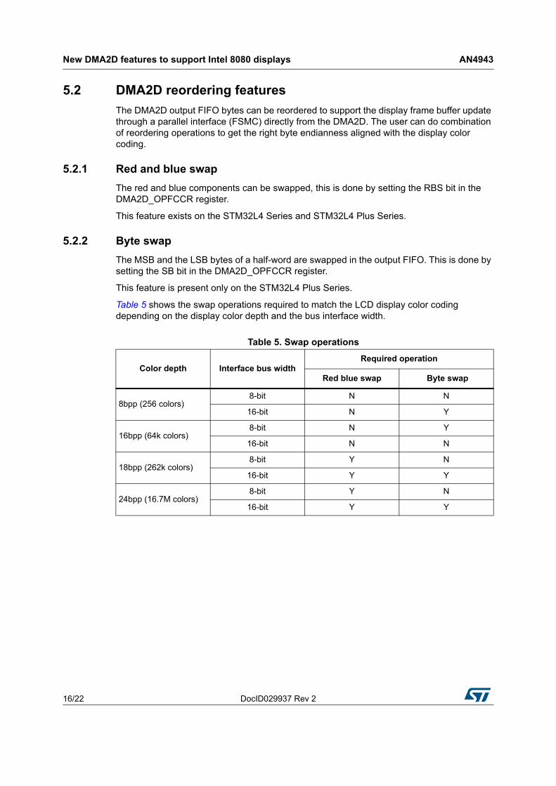
5.2 DMA2D reordering features
The DMA2D output FIFO bytes can be reordered to support the display frame buffer update through a parallel interface (FSMC) directly from the DMA2D. The user can do combination of reordering operations to get the right byte endianness aligned with the display color coding.
5.2.1 Red and blue swap
The red and blue components can be swapped, this is done by setting the RBS bit in the DMA2D_OPFCCR register.
This feature exists on the STM32L4 Series and STM32L4 Plus Series.
5.2.2 Byte swap
The MSB and the LSB bytes of a half-word are swapped in the output FIFO. This is done by setting the SB bit in the DMA2D_OPFCCR register.
This feature is present only on the STM32L4 Plus Series.
Table 5 shows the swap operations required to match the LCD display color coding depending on the display color depth and the bus interface width.
Table 5. Swap operations
Color depth Interface bus widthRequired operation
Red blue swap Byte swap
8bpp (256 colors)8-bit N N
16-bit N Y
16bpp (64k colors)8-bit N Y
16-bit N N
18bpp (262k colors)8-bit Y N
16-bit Y Y
24bpp (16.7M colors)8-bit Y N
16-bit Y Y

DocID029937 Rev 2 17/22
AN4943 New DMA2D features to support Intel 8080 displays
21
5.3 DMA2D reordering use case examples
5.3.1 24bpp/18bpp over 16-bit FSMC data bus interface
In order to support 24bpp displays using the 8080 standard, two operations are required on the frame buffer data:
• Red and blue swap
• MSB and LSB bytes of a half-word swap
Figure 8 shows the operations performed by the DMA2D allowing to have the good byte order corresponding to the Intel 8080 protocol for 24bpp color depth over a 16-bit interface.
Figure 8. DMA2D operations to support 24bpp over 16-bit interface
Note: On MCUs not supporting the byte swap, a hardware fix can be implemented by swapping the data lines of the LCD interface on the board. The display D[15:8] lines are connected to the FSMC D[7:0] lines and the display D[7:0] lines are connected to the FSMC D[15:8] lines.
MSv48350V1
B0 [7]B0 [6]B0 [5]B0 [4]B0 [3]B0 [2]B0 [1]B0 [0]
G0 [7]G0 [6]G0 [5]G0 [4]G0 [3]G0 [2]G0 [1]G0 [0]
R0 [7]R0 [6]R0 [5]R0 [4]R0 [3]R0 [2]R0 [1]R0 [0]
@+0
@+1
@+2
B1 [7]B1 [6]B1 [5]B1 [4]B1 [3]B1 [2]B1 [1]B1 [0]@+3
Memory
16-bit FSMC data bus
Pixel 0
Pixel 1
B0 [7]B0 [6]B0 [5]B0 [4]B0 [3]B0 [2]B0 [1]B0 [0]
G0 [7]G0 [6]G0 [5]G0 [4]G0 [3]G0 [2]G0 [1]G0 [0]
R0 [7]R0 [6]R0 [5]R0 [4]R0 [3]R0 [2]R0 [1]R0 [0]
D15D14D13D12D11D10D9D8D7D6D5D4D3D2D1D0
B0 [7]B0 [6]B0 [5]B0 [4]B0 [3]B0 [2]B0 [1]B0 [0]G0 [7]G0 [6]G0 [5]G0 [4]G0 [3]G0 [2]G0 [1]G0 [0]R0 [7]R0 [6]R0 [5]R0 [4]R0 [3]R0 [2]R0 [1]R0 [0]
R1 [7]R1 [6]R1 [5]R1 [4]R1 [3]R1 [2]R1 [1]R1 [0]
Red blue swap
R1 [7]R1 [6]R1 [5]R1 [4]R1 [3]R1 [2]R1 [1]R1 [0]
Byte swap
@+0
@+1
@+2
@+3
G0 [7]G0 [6]G0 [5]G0 [4]G0 [3]G0 [2]G0 [1]G0 [0]
R0 [7]R0 [6]R0 [5]R0 [4]R0 [3]R0 [2]R0 [1]R0 [0]
R1 [7]R1 [6]R1 [5]R1 [4]R1 [3]R1 [2]R1 [1]R1 [0]
B0 [7]B0 [6]B0 [5]B0 [4]B0 [3]B0 [2]B0 [1]B0 [0]
1 2Transfer number
Pixel 0
@+0
@+1
@+2
@+3
Pixel 1
Green component
Red component
Blue component

New DMA2D features to support Intel 8080 displays AN4943
18/22 DocID029937 Rev 2
5.3.2 24bpp/18bpp over 8-bit FSMC data bus interface
The red and blue swaps are required to get the correct order of bytes for 24bpp displays using an 8-bit data bus.
Figure 9 shows the red and blue swap operation done by the DMA2D allowing to have the good bytes order.
Figure 9. DMA2D operations to support 24bpp over 8-bit interface
MSv48351V1
8-bit FSMC data bus
B0 [7]B0 [6]B0 [5]B0 [4]B0 [3]B0 [2]B0 [1]B0 [0]
G0 [7]G0 [6]G0 [5]G0 [4]G0 [3]G0 [2]G0 [1]G0 [0]
R0 [7]R0 [6]R0 [5]R0 [4]R0 [3]R0 [2]R0 [1]R0 [0]
1 2 3 4Transfer number
R1 [7]R1 [6]R1 [5]R1 [4]R1 [3]R1 [2]R1 [1]R1 [0]
B0 [7]B0 [6]B0 [5]B0 [4]B0 [3]B0 [2]B0 [1]B0 [0]
G0 [7]G0 [6]G0 [5]G0 [4]G0 [3]G0 [2]G0 [1]G0 [0]
R0 [7]R0 [6]R0 [5]R0 [4]R0 [3]R0 [2]R0 [1]R0 [0]
@+0
@+1
@+2
B1 [7]B1 [6]B1 [5]B1 [4]B1 [3]B1 [2]B1 [1]B1 [0]@+3
Memory
Pixel 0
Pixel 1
B0 [7]B0 [6]B0 [5]B0 [4]B0 [3]B0 [2]B0 [1]B0 [0]G0 [7]G0 [6]G0 [5]G0 [4]G0 [3]G0 [2]G0 [1]G0 [0]R0 [7]R0 [6]R0 [5]R0 [4]R0 [3]R0 [2]R0 [1]R0 [0]
R1 [7]R1 [6]R1 [5]R1 [4]R1 [3]R1 [2]R1 [1]R1 [0]
Red blue swap
@+0
@+1
@+2
@+3
D7D6D5D4D3D2D1D0
Pixel 0 Pixel 1
Green component
Red component
Blue component

DocID029937 Rev 2 19/22
AN4943 New DMA2D features to support Intel 8080 displays
21
5.3.3 16bpp over 8-bit FSMC data bus interface
In order to drive the 16bpp Intel 8080 display over an 8-bit interface, the MSB and LSB bytes of a half word must be swapped.
Figure 10 shows how the swap operation allows having the good bytes order.
Figure 10. DMA2D operations to support 16bpp over 8-bit interface
MSv48352V1
@+0
@+1
@+2
@+3
Memory
Pixel 0
Pixel 1
8-bit FSMC data bus
1 2 3 4Transfer number
D7D6D5D4D3D2D1D0
R0 [4]R0 [3]R0 [2]R0 [1]R0 [0]G0 [5]G0 [4]G0 [3]G0 [2]G0 [1]G0 [0]B0 [4]B0 [3]B0 [2]B0 [1]B0 [0]
R1 [4]R1 [3]R1 [2]R1 [1]R1 [0]G1 [5]G1 [4]G1 [3]G1 [2]G1 [1]G1 [0]B1 [4]B1 [3]B1 [2]B1 [1]B1 [0]
R0 [4]R0 [3]R0 [2]R0 [1]R0 [0]G0 [5]G0 [4]G0 [3]
G0 [2]G0 [1]G0 [0]B0 [4]B0 [3]B0 [2]B0 [1]B0 [0]
R1 [4]R1 [3]R1 [2]R1 [1]R1 [0]G1 [5]G1 [4]G1 [3]
G1 [2]G1 [1]G1 [0]B1 [4]B1 [3]B1 [2]B1 [1]B1 [0]
Byte swap
R0 [4]R0 [3]R0 [2]R0 [1]R0 [0]G0 [5]G0 [4]G0 [3]
G0 [2]G0 [1]G0 [0]B0 [4]B0 [3]B0 [2]B0 [1]B0 [0]
R1 [4]R1 [3]R1 [2]R1 [1]R1 [0]G1 [5]G1 [4]G1 [3]
G1 [2]G1 [1]G1 [0]B1 [4]B1 [3]B1 [2]B1 [1]B1 [0]
Pixel 0 Pixel 1
@+0
@+1
@+2
@+3
Green component
Red component
Blue component

Conclusion AN4943
20/22 DocID029937 Rev 2
6 Conclusion
This application note gives a guideline to easily transfer images to an LCD-TFT display via the FSMC interface using the Chrom-ART Accelerator™ (DMA2D) without using the CPU or the DMA resources. A focus is given to the correct control of the 'Data/command control' signal of the LCD-TFT display. Some code examples have also been provided to setup the Chrom-ART Accelerator™ (DMA2D).
This application note also presents the new byte reordering features of the DMA2D allowing to support an update of 16.7M color and 262k color Intel 8080 displays directly through the FSMC.
DocID029937 Rev 2 21/22
AN4943 Revision history
21
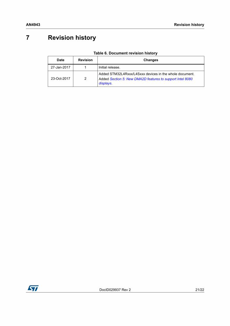
7 Revision history
Table 6. Document revision history
Date Revision Changes
27-Jan-2017 1 Initial release.
23-Oct-2017 2Added STM32L4Rxxx/L4Sxxx devices in the whole document.
Added Section 5: New DMA2D features to support Intel 8080 displays.

AN4943
22/22 DocID029937 Rev 2
IMPORTANT NOTICE – PLEASE READ CAREFULLY
STMicroelectronics NV and its subsidiaries (“ST”) reserve the right to make changes, corrections, enhancements, modifications, and improvements to ST products and/or to this document at any time without notice. Purchasers should obtain the latest relevant information on ST products before placing orders. ST products are sold pursuant to ST’s terms and conditions of sale in place at the time of order acknowledgement.
Purchasers are solely responsible for the choice, selection, and use of ST products and ST assumes no liability for application assistance or the design of Purchasers’ products.
No license, express or implied, to any intellectual property right is granted by ST herein.
Resale of ST products with provisions different from the information set forth herein shall void any warranty granted by ST for such product.
ST and the ST logo are trademarks of ST. All other product or service names are the property of their respective owners.
Information in this document supersedes and replaces information previously supplied in any prior versions of this document.
© 2017 STMicroelectronics – All rights reserved