Directors and Officers Underwriter Meetings Cirrus Logic, Inc. September 9-13, 2004 Confidential.
AN298
CS485xx Firmware User’s Manual: General Overview and Common Firmware Modules
Contents
Document Strategy
Overview
Firmware Messaging
OS Firmware Module
Audio Manager Firmware Module
PCM Firmware Module
Low Power Mode
Watchdog Timer
Document Revisions
Overview
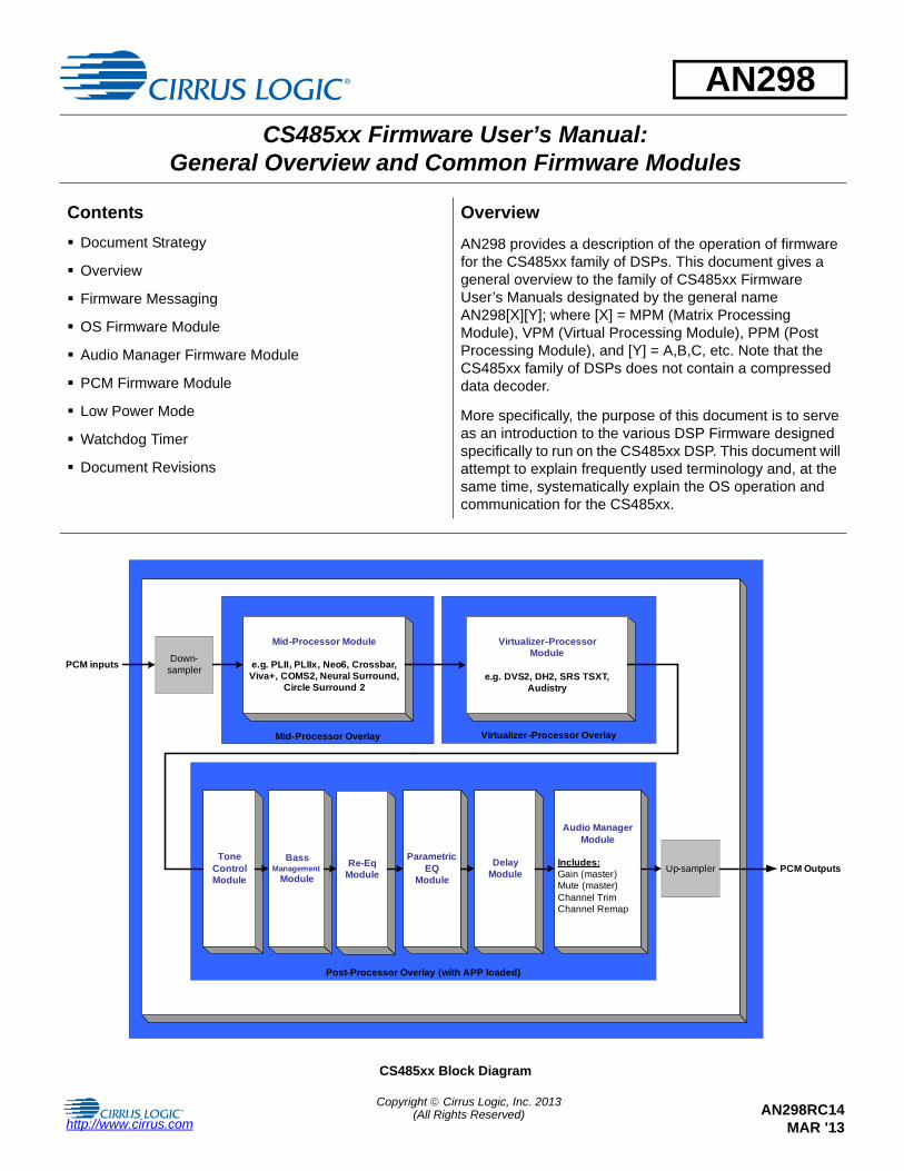
AN298 provides a description of the operation of firmware for the CS485xx family of DSPs. This document gives a general overview to the family of CS485xx Firmware User’s Manuals designated by the general name AN298[X][Y]; where [X] = MPM (Matrix Processing Module), VPM (Virtual Processing Module), PPM (Post Processing Module), and [Y] = A,B,C, etc. Note that the CS485xx family of DSPs does not contain a compressed data decoder.
More specifically, the purpose of this document is to serve as an introduction to the various DSP Firmware designed specifically to run on the CS485xx DSP. This document will attempt to explain frequently used terminology and, at the same time, systematically explain the OS operation and communication for the CS485xx.
CS485xx Block Diagram
Mid-Processor Overlay
PCM Outputs
Post-Processor Overlay (with APP loaded)
ID = 0x83ID = 0xD9ID = 0xD5ID = 0xD4
Tone Control Module
Re-Eq Module
Bass Management
Module
Parametric EQ
Module
Delay Module
Audio Manager Module
Includes:Gain (master)Mute (master)Channel Trim Channel Remap
Up-sampler
Mid-Processor Module
e.g. PLII, PLIIx, Neo6, Crossbar, Viva+, COMS2, Neural Surround,
Circle Surround 2
Virtualizer-ProcessorModule
e.g. DVS2, DH2, SRS TSXT, Audistry
Virtualizer -Processor Overlay Mid-Processor Overlay
PCM inputsDown-
sampler
Copyright Cirrus Logic, Inc. 2013(All Rights Reserved)
http://www.cirrus.comAN298RC14
MAR '13
1 Document Strategy
1 Document Strategy
The CS485xx has been designed with an inherent flexibility in terms of firmware usage. Each instance of operation of the CS485xx can potentially use a different mix of DSP firmware depending on the need of the end user. As such, the strategy adopted to document the various DSP firmware is based on a single General Overview coupled with an individual Firmware User’s Manual for each DSP firmware module offered by Cirrus Logic. AN298 is the General Overview to the family of CS485xx Firmware User’s Manuals.
The individual Firmware User’s Manuals, mentioned in the above paragraph, each follow as an extension of AN298. These manuals have been named in such a way so as to classify them into one of the following categories:
• Operating System and General Overview
• Matrix Processing Module (MPM)
• Virtual Processing Module (VPM)
• Post Processing Module (PPM)
Furthermore, since each classification (e.g., Post Processing Module) may contain several associated DSP firmware, an incremental letter assignment (e.g., A, B, C etc.) was given to index each DSP firmware within a given category. As an example, the table below outlines the general naming conventions for several firmware modules.
For a further breakdown of the available CS485xx firmware modules and their respective Firmware User’s Guide document number, see Section 2.4. For the latest code updates and availability, contact your local field applications engineer (FAE).
Table 1-1. Naming Conventions
DSP Firmware Module Base Name Overlay Type Index Reference NumberGeneral Overview, Operating System & Common
Firmware ModulesAN298 (General) - AN298
Delay Module AN298 Post Processing Module (PPM) a AN298PPMACrossbar Mixer Module AN298 Matrix Processing Module (MPM) c AN298MPMC
Dolby Headphone 2 AN298 Virtual Processing Module (VPM) a AN298VPMA
2 AN298RC14
2 Overview
2 Overview
The firmware that runs on this device expects a stereo or multi-channel PCM input source. This section describes the different overlays as well as the functionality of the various processor module overlays.
Figure 2-1. CS485xx Firmware Block Diagram
2.1 Firmware Overlays
The data flows through a series of four firmware overlays that contain one or more firmware modules. A firmware module provides the specific application affectionately and is controlled by the host via a Firmware Manager that defines the control interface. The overlays segment the firmware module functionality into four independent groups depending on function:
OS Overlay
• Manages the overall operation of the DSP. Also handles host communication, data inputs and outputs and various other critical internal tasks.
Matrix Processing Module Overlay
• Performs additional channel generation, upmixing, downmixing. This segment is where algorithms such as Pro Logic® IIx, Neo6™, and COMS2 reside.
Virtual Processing Module Overlay
• Performs stereo virtualizing to simulate multi-channel systems, such as Dolby® Audistry®, Dolby Headphone®, and Dolby Virtual Surround®.
Post Processing Module Overlay
• This segment specifically caters to firmware that performs post-processing tasks. It allows the system designer flexibility in “tweaking” the system for optimal audio performance and effects. This is also the segment in which firmware modules such as the Audio Manager, Bass Manager, Tone Control, Delay, THX®, and Parametric-EQ Module will reside.
Mid-Processor Overlay
PCM Outputs
Post-Processor Overlay (with APP loaded)
ID = 0x83ID = 0xD9ID = 0xD5ID = 0xD4
Tone Control Module
Re-Eq Module
Bass Management
Module
Parametric EQ
Module
Delay Module
Audio Manager Module
Includes:Gain (master)Mute (master)Channel Trim Channel Remap
Up-sampler
Mid-Processor Module
e.g. PLII, PLIIx, Neo6, Crossbar, Viva+, COMS2, Neural Surround,
Circle Surround 2
Virtualizer-ProcessorModule
e.g. DVS2, DH2, SRS TSXT, Audistry
Virtualizer-Processor Overlay Mid-Processor Overlay
PCM inputsDown-
sampler
AN298RC14 3
2.2 Code Image (.uld) Files
2.2 Code Image (.uld) Files
Each overlay is a separate code image file (.uld) that is loaded individually into the DSP. To change the functionality of the application, only the overlay of interest needs to be loaded. For example the Post Processing overlay can be exchanged from SPP to APP by reloading only the Post Processing overlay. This reduces the system response time to user changes as well as the code image storage requirements.
Note: There are 4 different memory configurations pertaining to the program RAM size (most code is in ROM). The different memory configurations are denoted by p2, p4, p6, and p8 (p for program memory, 2, 4, 6, and 8 are the number of kilo-words, 1 word = 32 bits). Increasing P RAM decreases Y RAM. Each overlay is denoted with the p2, p4, p6, or p8 in the .uld file name to indicate which memory configuration is used.
WARNING: Memory configuration must be consistent across all overlays (OS, MPM, VPM, and PPM).
2.2.1 .uld File Naming Conventions
A generic template for representing .uld file can be represented by the following file name:
AA_48BBB_pC_DD_EE_rcFF.uld
2.2.1.1 .uld File Name Variables
• AA = Technology name (os, mb, app, spp, …)
• BBB = minimum chip required to run the firmware loaded by the .uld file (520, 560, dv2, au2)
• 520 means this will run on a 520, 540, & 560
• 540 means this will run on a 540 & 560 (Not on a 520)
• 560 means this will run on a 560 (Not on a 520 or 540)
• dv2 means this will run on a CS48DV2x DSP only
• au2 mean this will run on a CS48AU2B only
• C = memory configuration (2, 4, 6, or 8)
This is the amount of PRAM in Kilowords (1 word = 32-bits). More PRAM means less YRAM.
The memory configurations can be broken down into the following categories:
• P2
• X Memory - 8kx32 SRAM, 8kx32 DROM
• Y Memory - 14kx32 SRAM, 8kx32 DROM
• P Memory - 2kx32 SRAM, 32kx32 DROM
• P4
• X Memory - 8kx32 SRAM, 8kx32 DROM
• Y Memory - 12kx32 SRAM, 8kx32 DROM
• P Memory - 4kx32 SRAM, 32kx32 DROM
• P6
• X Memory - 8kx32 SRAM, 8kx32 DROM
• Y Memory - 10kx32 SRAM, 8kx32 DROM
• P Memory - 6kx32 SRAM, 32kx32 DROM
• P8
• X Memory - 8kx32 SRAM, 8kx32 DROM
• Y Memory - 8kx32 SRAM, 8kx32 DROM
• P Memory - 8kx32 SRAM, 32kx32 DROM
• DD = Firmware version
4 AN298RC14
2.3 Download Sequence
This variable is the specific memory map for the various overlays and can be specific to a particular version of ROM
Current Firmware versions are:
• 01 = CS485xx
• 02 =CS48DV2A
• 03 = CS48DV2B
• 04 = CS485xx
• 05 = CS485xx
• 06 = CS48AU2B
• 09 = CS485xx
• EE = This variable indicates a major revision, increments when rc99 -> rc1
• FF = This Variable indicates a minor revision, increments by one for each new .uld build
2.2.1.2 Example of .uld file name
An example of a .uld file name:
os_48520_p2_48520_01_01_rc5.uld
• AA = os (DSPP operating system)
• BBB = CS48520 (this .uld will run on CS48520, CS48540, and CS48560)
• C = p2
• DD = 01 (all other overlays that are loaded on the DSP must be 01 overlays)
• EE = 01 (have not made over 100 of these)
• FF = rc5
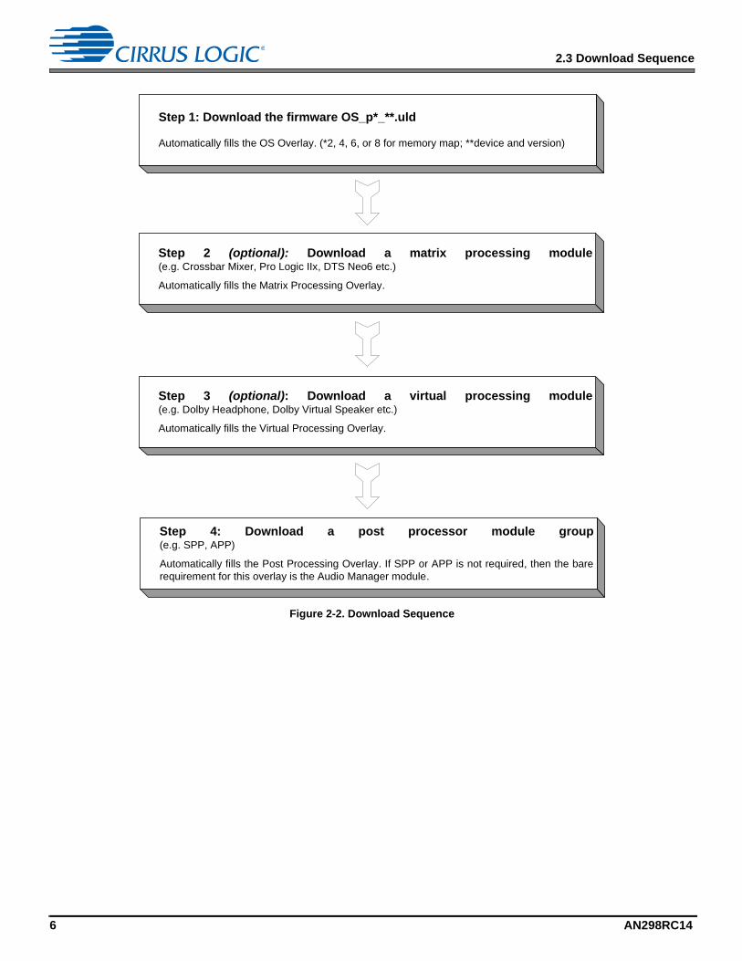
2.3 Download Sequence
A standard procedure to download firmware to the DSP follows the following structure at system power-up:
1. Download OS Overlays to DSP
2. (optional) Download Matrix Processing Module Overlay (Crossbar Mixer, Pro Logic IIx, DTS Neo6 etc.)
3. (optional) Download Virtual Processing Module Overlay (COMS2)
4. (optional) Download Post Processing Module Overlay (Audio Manager, Bass Manager, Delay, Parametric EQ, etc.)
AN298RC14 5
2.3 Download Sequence
Figure 2-2. Download Sequence
Step 2 (optional): Download a matrix processing module (e.g. Crossbar Mixer, Pro Logic IIx, DTS Neo6 etc.)
Automatically fills the Matrix Processing Overlay.
Step 3 (optional): Download a virtual processing module (e.g. Dolby Headphone, Dolby Virtual Speaker etc.)
Automatically fills the Virtual Processing Overlay.
Step 4: Download a post processor module group (e.g. SPP, APP)
Automatically fills the Post Processing Overlay. If SPP or APP is not required, then the bare requirement for this overlay is the Audio Manager module.
Step 1: Download the firmware OS_p*_**.uld
Automatically fills the OS Overlay. (*2, 4, 6, or 8 for memory map; **device and version)
6 AN298RC14
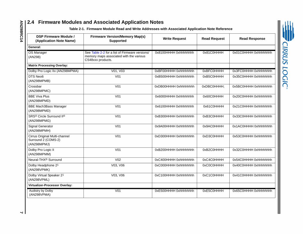
AN 2.4 Firmware Modules and Associated Application Notes
eference
uest Read Response
HH 0x01C0HHHH 0xhhhhhhhh
HHH 0x3FC0HHHH 0xhhhhhhhh
HH 0x35C0HHHH 0xhhhhhhhh
HH; 0x5BC0HHHH 0xhhhhhhhh
HH 0x20C0HHHH 0xhhhhhhhh
HHH 0x21C0HHHH 0xhhhhhhhh
HH 0x33C0HHHH 0xhhhhhhhh
HH 0x1AC0HHHH 0xhhhhhhhh
HHH 0x53C0HHHH 0xhhhhhhhh
HH 0x32C0HHHH 0xhhhhhhhh
HHH 0x54C0HHHH 0xhhhhhhhh
HHH 0x40C0HHHH 0xhhhhhhhh
HHH 0x41C0HHHH 0xhhhhhhhh
HH 0x65C0HHHH 0xhhhhhhhh
29
8RC
147
Table 2-1. Firmware Module Read and Write Addresses with Associated Application Note R
DSP Firmware Module / (Application Note Name)
Firmware Version/Memory Map(s) Supported
Write Request Read Req
General:
OS Manager (AN298)
See Table 2-2 for a list of Firmware versions/ memory maps associated with the various CS48xxx products.
0x8100HHHH 0xhhhhhhhh 0x81C0HH
Matrix Processing Overlay:
Dolby Pro Logic IIx (AN298MPMA) V01, V03 0xBF00HHHH 0xhhhhhhhh 0xBFC0H
DTS Neo6(AN298MPMB)
V01 0xB500HHHH 0xhhhhhhhh 0xB5C0HH
Crossbar(AN298MPMC)
V01 0xDB00HHHH 0xhhhhhhhh 0xDBC0HH
BBE Viva Plus(AN298MPMD)
V01 0x6000HHHH 0xhhhhhhhh 0x60C0HH
BBE Mach3Bass Manager(AN298MPMD)
V01 0x6100HHHH 0xhhhhhhhh 0x61C0H
SRS® Circle Surround II®
(AN298MPMG)V01 0xB300HHHH 0xhhhhhhhh 0xB3C0HH
Signal Generator(AN298MPMH)
V01 0x9A00HHHH 0xhhhhhhhh 0x9AC0HH
Cirrus Original Multi-channel Surround 2 (COMS-2)(AN298MPMJ)
V01 0xD300HHHH 0xhhhhhhhh 0xD3C0H
Dolby Pro Logic II(AN298MPMM)
V01 0xB200HHHH 0xhhhhhhhh 0xB2C0HH
Neural-THX® Surround V02 0xC400HHHH 0xhhhhhhhh 0xC4C0H
Dolby Headphone 21
(AN298VPMK)V03, V06 0xC000HHHH 0xhhhhhhhh 0xC0C0H
Dolby Virtual Speaker 21
(AN298VPML)V03, V06 0xC100HHHH 0xhhhhhhhh 0xC1C0H
Virtualizer-Processor Overlay:
Audistry by Dolby(AN298VPMA)
V01 0xE500HHHH 0xhhhhhhhh 0xE5C0HH
AN
HHH 0x3AC0HHHH 0xhhhhhhhh
HHH 0x40C0HHHH 0xhhhhhhhh
HHH 0x41C0HHHH 0xhhhhhhhh
HH 0x33C0HHHH 0xhhhhhhhh
HHH 0x41C0HHHH 0xhhhhhhhh
HH 0x03c0HHHH 0xhhhhhhhh
HH 0x1BC0HHHH 0xhhhhhhhh
HHH 0x59C0HHHH 0xhhhhhhhh
HHH 0x57C0HHHH 0xhhhhhhhh
HHH 0x67C0HHHH 0xhhhhhhhh
HH 0x67C0HHHH 0xhhhhhhhh
HHH 0x55C0HHHH 0xhhhhhhhh
HHH 0x54C0HHHH 0xhhhhhhhh
HH 0x60C0HHHH 0xhhhhhhhh
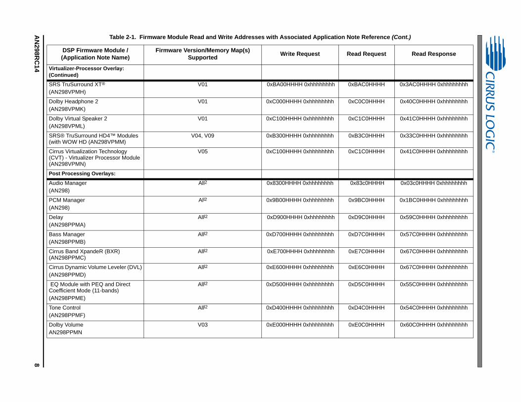
Table 2-1. Firmware Module Read and Write Addresses with Associated Application Note Reference (Cont.)
uest Read Response
29
8RC
148
Virtualizer-Processor Overlay: (Continued)
SRS TruSurround XT®
(AN298VPMH)V01 0xBA00HHHH 0xhhhhhhhh 0xBAC0H
Dolby Headphone 2(AN298VPMK)
V01 0xC000HHHH 0xhhhhhhhh 0xC0C0H
Dolby Virtual Speaker 2(AN298VPML)
V01 0xC100HHHH 0xhhhhhhhh 0xC1C0H
SRS® TruSurround HD4™ Modules (with WOW HD (AN298VPMM)
V04, V09 0xB300HHHH 0xhhhhhhhh 0xB3C0HH
Cirrus Virtualization Technology (CVT) - Virtualizer Processor Module (AN298VPMN)
V05 0xC100HHHH 0xhhhhhhhh 0xC1C0H
Post Processing Overlays:
Audio Manager (AN298)
All2 0x8300HHHH 0xhhhhhhhh 0x83c0HH
PCM Manager(AN298)
All2 0x9B00HHHH 0xhhhhhhhh 0x9BC0HH
Delay(AN298PPMA)
Alll2 0xD900HHHH 0xhhhhhhhh 0xD9C0H
Bass Manager(AN298PPMB)
Alll2 0xD700HHHH 0xhhhhhhhh 0xD7C0H
Cirrus Band XpandeR (BXR) (AN298PPMC)
Alll2 0xE700HHHH 0xhhhhhhhh 0xE7C0H
Cirrus Dynamic Volume Leveler (DVL)(AN298PPMD)
Alll2 0xE600HHHH 0xhhhhhhhh 0xE6C0HH
EQ Module with PEQ and Direct Coefficient Mode (11-bands)(AN298PPME)
Alll2 0xD500HHHH 0xhhhhhhhh 0xD5C0H
Tone Control(AN298PPMF)
Alll2 0xD400HHHH 0xhhhhhhhh 0xD4C0H
Dolby VolumeAN298PPMN
V03 0xE000HHHH 0xhhhhhhhh 0xE0C0HH
DSP Firmware Module / (Application Note Name)
Firmware Version/Memory Map(s) Supported
Write Request Read Req
AN
HHH 0x5CC0HHHH 0xhhhhhhhh
HHH 0x60C0HHHH 0xhhhhhhhh
HH 0x68C0HHHH 0xhhhhhhhh
HHH 0x47C0HHHH 0xhhhhhhhh
HHH 0x48C0HHHH 0xhhhhhhhh
HHH 0xC9C0HHHH 0xhhhhhhhh
HHH 0x6DC0HHHH 0xhhhhhhhh
Table 2-1. Firmware Module Read and Write Addresses with Associated Application Note Reference (Cont.)
uest Read Response
29
8RC
149
Post Processing Overlays:(Continued)
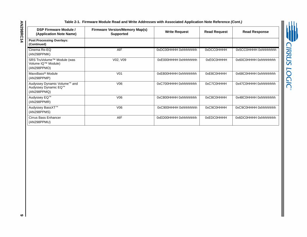
Cinema Re-EQ(AN298PPMK)
All2 0xDC00HHHH 0xhhhhhhhh 0xDCC0H
SRS TruVolume™ Module (was Volume IQ™ Module)(AN298PPMO)
V02, V09 0xE000HHHH 0xhhhhhhhh 0xE0C0H
MaxxBass® Module (AN298PPMP)
V01 0xE800HHHH 0xhhhhhhhh 0xE8C0HH
Audyssey Dynamic Volume™ and Audyssey Dynamic EQ™
(AN298PPMQ)
V06 0xC700HHHH 0xhhhhhhhh 0xC7C0H
Audyssey EQ™
(AN298PPMR)V06 0xC800HHHH 0xhhhhhhhh 0xC8C0H
Audyssey BassXT™
(AN298PPMS)V06 0xC900HHHH 0xhhhhhhhh 0xC9C0H
Cirrus Bass Enhancer (AN298PPMU)
All2 0xED00HHHH 0xhhhhhhhh 0xEDC0H
DSP Firmware Module / (Application Note Name)
Firmware Version/Memory Map(s) Supported
Write Request Read Req
AN
HHH 0x49C0HHHH 0xhhhhhhhh
48DV2B DSPs. Dolby Headphone 2 and ersions/memory maps.t (.o) file and compiled into an .uld file,
Table 2-1. Firmware Module Read and Write Addresses with Associated Application Note Reference (Cont.)
uest Read Response
29
8RC
141
0
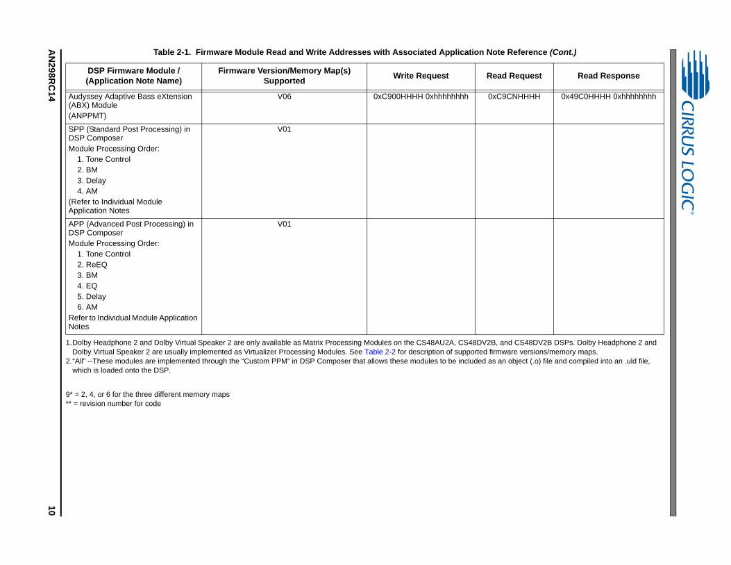
9* = 2, 4, or 6 for the three different memory maps** = revision number for code
Audyssey Adaptive Bass eXtension (ABX) Module(ANPPMT)
V06 0xC900HHHH 0xhhhhhhhh 0xC9CNH
SPP (Standard Post Processing) in DSP ComposerModule Processing Order: 1. Tone Control 2. BM 3. Delay 4. AM(Refer to Individual Module Application Notes
V01
APP (Advanced Post Processing) in DSP ComposerModule Processing Order: 1. Tone Control 2. ReEQ 3. BM 4. EQ 5. Delay 6. AMRefer to Individual Module Application Notes
V01
1.Dolby Headphone 2 and Dolby Virtual Speaker 2 are only available as Matrix Processing Modules on the CS48AU2A, CS48DV2B, and CSDolby Virtual Speaker 2 are usually implemented as Virtualizer Processing Modules. See Table 2-2 for description of supported firmware v
2.“All” --These modules are implemented through the “Custom PPM” in DSP Composer that allows these modules to be included as an objecwhich is loaded onto the DSP.
DSP Firmware Module / (Application Note Name)
Firmware Version/Memory Map(s) Supported
Write Request Read Req
2.4 Firmware Modules and Associated Application Notes
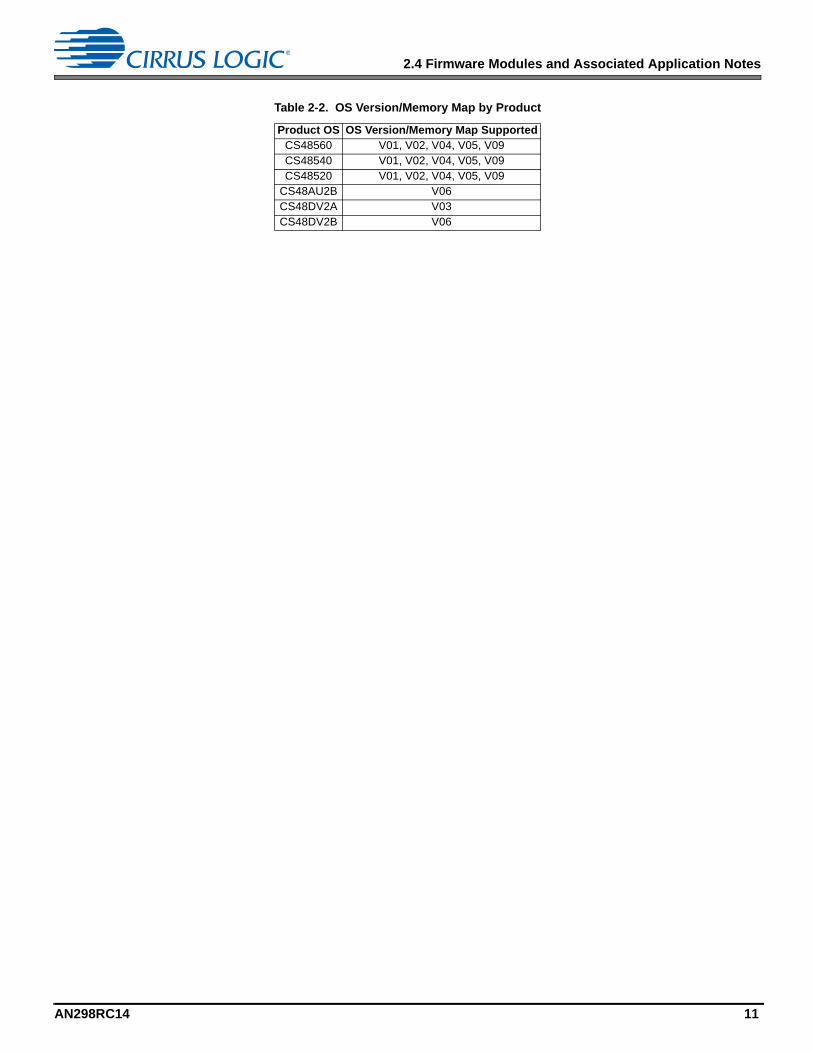
Table 2-2. OS Version/Memory Map by Product
Product OS OS Version/Memory Map SupportedCS48560 V01, V02, V04, V05, V09CS48540 V01, V02, V04, V05, V09CS48520 V01, V02, V04, V05, V09
CS48AU2B V06CS48DV2A V03CS48DV2B V06
AN298RC14 11
3 Firmware Messaging
3 Firmware Messaging
While using the CS485xx, it is necessary to communicate with the DSP in order to control or monitor the various downloaded firmware modules. We refer to this process of communication firmware messaging. The purpose of this section is to cover the types and formats of these firmware messages. In general, with firmware messaging, the user can control the firmware module running on the DSP and subsequently perform various tasks such as:
• Configure the module after firmware download (e.g. Kickstarting the DSP, etc.)
• Change runtime parameters (e.g. adjusting the Volume, switching Pro Logic II modes, etc.)
• Obtain information from the DSP (e.g. current state of the firmware registers, data stream information, etc.)
3.1 Communication Overview
From a “micro-programmer” point of view, the CS485xx firmware modules can be thought of as a blocks of several 32-bit registers (variables) that either control the behavior of the firmware or store information about the state of the firmware at the time of operation. Each register has a unique index. Access to the register involves a combination of a specified opcode for that firmware module together with the register index. For each firmware module, the following opcodes are available:
• Write Opcode - Issues a command to write to a specific module.
• Read Opcode - Issues a command to read from a specific module.
• Read Response Opcode - Indicates module and index that has been read.
These available opcodes permit the following types of communication with the CS485xx DSP:
• Writing to the DSP
• Solicited read from the DSP
• Unsolicited read from the DSP
The following sub-sections cover the communication types listed above.
3.1.1 Writing to the DSP
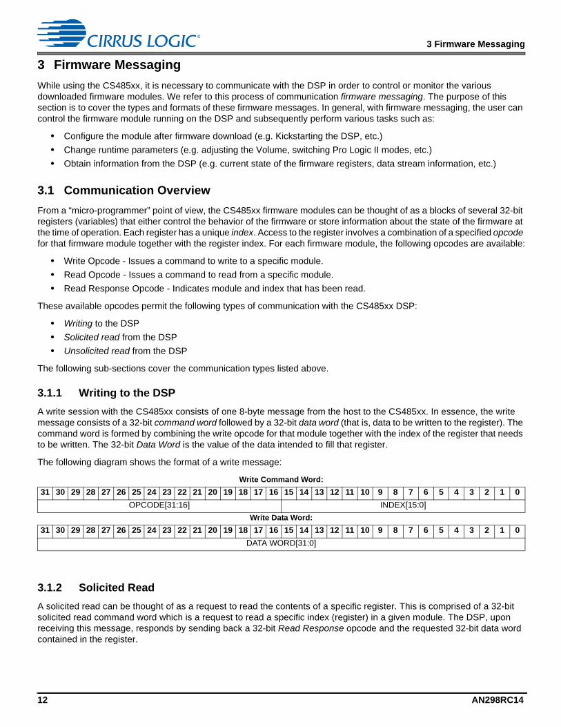
A write session with the CS485xx consists of one 8-byte message from the host to the CS485xx. In essence, the write message consists of a 32-bit command word followed by a 32-bit data word (that is, data to be written to the register). The command word is formed by combining the write opcode for that module together with the index of the register that needs to be written. The 32-bit Data Word is the value of the data intended to fill that register.
The following diagram shows the format of a write message:
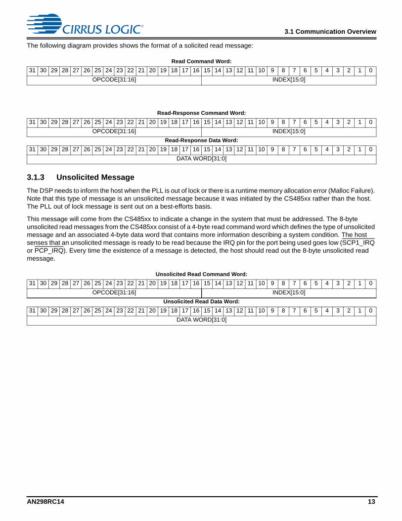
3.1.2 Solicited Read
A solicited read can be thought of as a request to read the contents of a specific register. This is comprised of a 32-bit solicited read command word which is a request to read a specific index (register) in a given module. The DSP, upon receiving this message, responds by sending back a 32-bit Read Response opcode and the requested 32-bit data word contained in the register.
Write Command Word:
31 30 29 28 27 26 25 24 23 22 21 20 19 18 17 16 15 14 13 12 11 10 9 8 7 6 5 4 3 2 1 0
OPCODE[31:16] INDEX[15:0]
Write Data Word:
31 30 29 28 27 26 25 24 23 22 21 20 19 18 17 16 15 14 13 12 11 10 9 8 7 6 5 4 3 2 1 0
DATA WORD[31:0]
12 AN298RC14
3.1 Communication Overview
The following diagram provides shows the format of a solicited read message:
3.1.3 Unsolicited Message
The DSP needs to inform the host when the PLL is out of lock or there is a runtime memory allocation error (Malloc Failure). Note that this type of message is an unsolicited message because it was initiated by the CS485xx rather than the host. The PLL out of lock message is sent out on a best-efforts basis.
This message will come from the CS485xx to indicate a change in the system that must be addressed. The 8-byte unsolicited read messages from the CS485xx consist of a 4-byte read command word which defines the type of unsolicited message and an associated 4-byte data word that contains more information describing a system condition. The host senses that an unsolicited message is ready to be read because the IRQ pin for the port being used goes low (SCP1_IRQ or PCP_IRQ). Every time the existence of a message is detected, the host should read out the 8-byte unsolicited read message.
Read Command Word:
31 30 29 28 27 26 25 24 23 22 21 20 19 18 17 16 15 14 13 12 11 10 9 8 7 6 5 4 3 2 1 0
OPCODE[31:16] INDEX[15:0]
Read-Response Command Word:
31 30 29 28 27 26 25 24 23 22 21 20 19 18 17 16 15 14 13 12 11 10 9 8 7 6 5 4 3 2 1 0
OPCODE[31:16] INDEX[15:0]
Read-Response Data Word:
31 30 29 28 27 26 25 24 23 22 21 20 19 18 17 16 15 14 13 12 11 10 9 8 7 6 5 4 3 2 1 0
DATA WORD[31:0]
Unsolicited Read Command Word:
31 30 29 28 27 26 25 24 23 22 21 20 19 18 17 16 15 14 13 12 11 10 9 8 7 6 5 4 3 2 1 0
OPCODE[31:16] INDEX[15:0]
Unsolicited Read Data Word:
31 30 29 28 27 26 25 24 23 22 21 20 19 18 17 16 15 14 13 12 11 10 9 8 7 6 5 4 3 2 1 0
DATA WORD[31:0]
AN298RC14 13
4 Operating System (OS) Firmware Module
4 Operating System (OS) Firmware Module
Indices of the Firmware Module can differ in properties that are important to the system firmware programmer.
Indices marked by a ‘†’ can be modified after kick-starting the application. However, indices not marked by a ‘†’ must be configured by the system host controller before the kick-start message is sent to begin decoding. For these indices, changes after kick-starting the application will not have the desired effect and can potentially cause the application to become unstable.
All indices are reinitialized to the default values after downloading the overlay and soft-resetting the overlay.
4.1 Overview
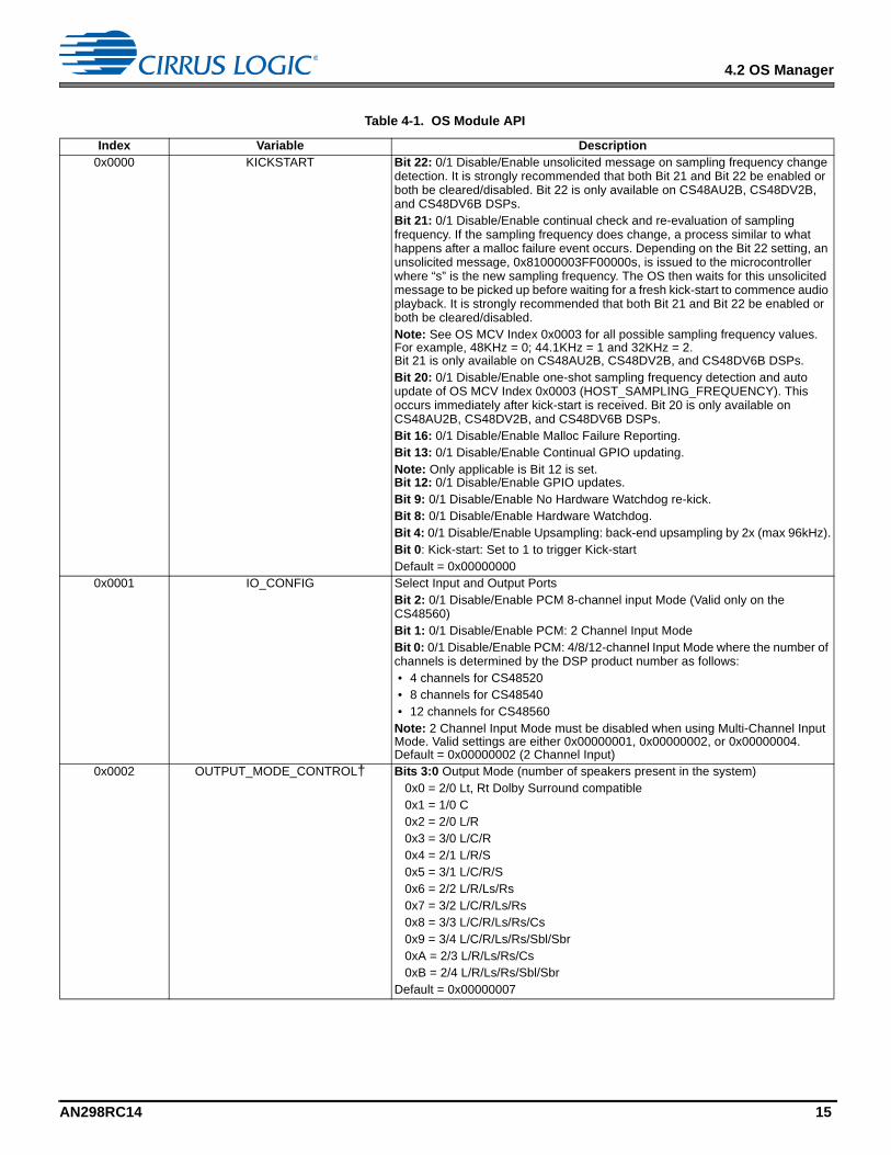
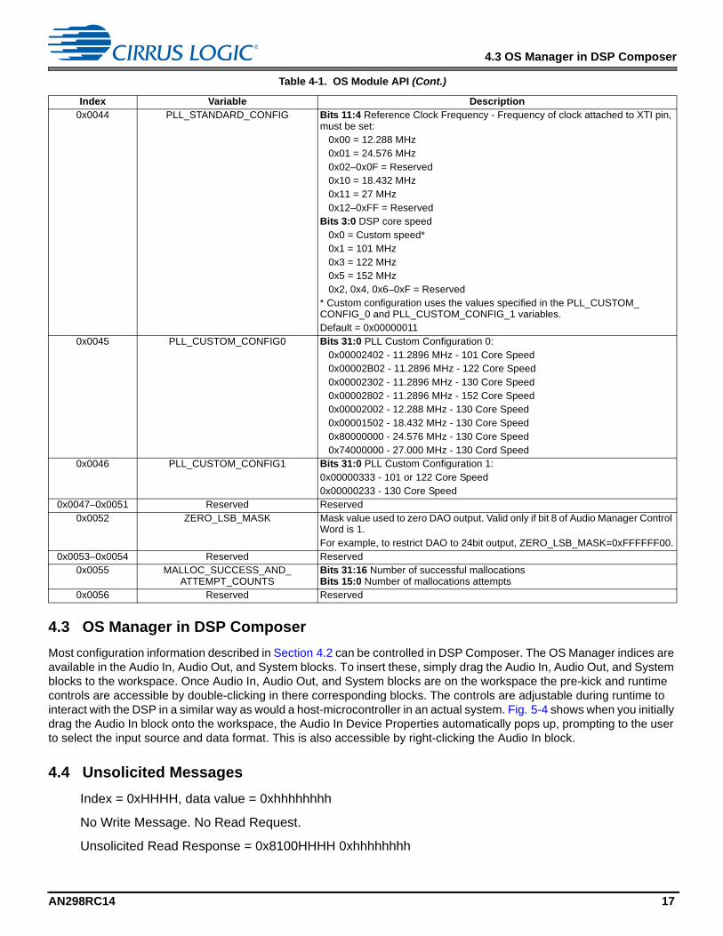
Table 4-1 contains the API used to control the OS firmware module.
4.2 OS Manager
Index = 0xHHHH, data value = 0xhhhhhhhh
Write = 0x8100HHHH 0xhhhhhhhh
Read Request = 0x81C0HHHH
Read Response = 0x01C0HHHH 0xhhhhhhhh
14 AN298RC14
4.2 OS Manager
Table 4-1. OS Module API
Index Variable Description0x0000 KICKSTART Bit 22: 0/1 Disable/Enable unsolicited message on sampling frequency change
detection. It is strongly recommended that both Bit 21 and Bit 22 be enabled or both be cleared/disabled. Bit 22 is only available on CS48AU2B, CS48DV2B, and CS48DV6B DSPs.Bit 21: 0/1 Disable/Enable continual check and re-evaluation of sampling frequency. If the sampling frequency does change, a process similar to what happens after a malloc failure event occurs. Depending on the Bit 22 setting, an unsolicited message, 0x81000003FF00000s, is issued to the microcontroller where “s” is the new sampling frequency. The OS then waits for this unsolicited message to be picked up before waiting for a fresh kick-start to commence audio playback. It is strongly recommended that both Bit 21 and Bit 22 be enabled or both be cleared/disabled.Note: See OS MCV Index 0x0003 for all possible sampling frequency values. For example, 48KHz = 0; 44.1KHz = 1 and 32KHz = 2.Bit 21 is only available on CS48AU2B, CS48DV2B, and CS48DV6B DSPs.Bit 20: 0/1 Disable/Enable one-shot sampling frequency detection and auto update of OS MCV Index 0x0003 (HOST_SAMPLING_FREQUENCY). This occurs immediately after kick-start is received. Bit 20 is only available on CS48AU2B, CS48DV2B, and CS48DV6B DSPs.Bit 16: 0/1 Disable/Enable Malloc Failure Reporting.Bit 13: 0/1 Disable/Enable Continual GPIO updating. Note: Only applicable is Bit 12 is set.Bit 12: 0/1 Disable/Enable GPIO updates. Bit 9: 0/1 Disable/Enable No Hardware Watchdog re-kick. Bit 8: 0/1 Disable/Enable Hardware Watchdog. Bit 4: 0/1 Disable/Enable Upsampling: back-end upsampling by 2x (max 96kHz).Bit 0: Kick-start: Set to 1 to trigger Kick-startDefault = 0x00000000
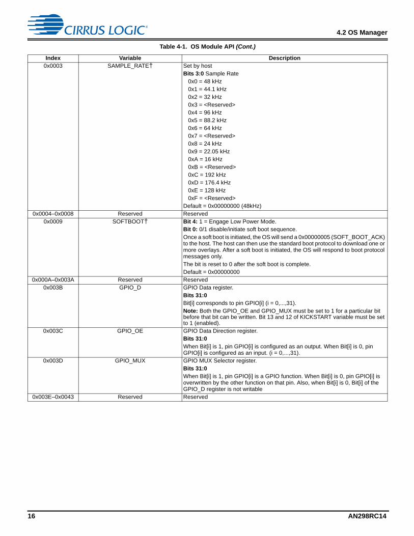
0x0001 IO_CONFIG Select Input and Output PortsBit 2: 0/1 Disable/Enable PCM 8-channel input Mode (Valid only on the CS48560)Bit 1: 0/1 Disable/Enable PCM: 2 Channel Input ModeBit 0: 0/1 Disable/Enable PCM: 4/8/12-channel Input Mode where the number of channels is determined by the DSP product number as follows: • 4 channels for CS48520 • 8 channels for CS48540 • 12 channels for CS48560Note: 2 Channel Input Mode must be disabled when using Multi-Channel Input Mode. Valid settings are either 0x00000001, 0x00000002, or 0x00000004.Default = 0x00000002 (2 Channel Input)
0x0002 OUTPUT_MODE_CONTROL† Bits 3:0 Output Mode (number of speakers present in the system)0x0 = 2/0 Lt, Rt Dolby Surround compatible0x1 = 1/0 C0x2 = 2/0 L/R0x3 = 3/0 L/C/R0x4 = 2/1 L/R/S0x5 = 3/1 L/C/R/S0x6 = 2/2 L/R/Ls/Rs0x7 = 3/2 L/C/R/Ls/Rs0x8 = 3/3 L/C/R/Ls/Rs/Cs0x9 = 3/4 L/C/R/Ls/Rs/Sbl/Sbr0xA = 2/3 L/R/Ls/Rs/Cs0xB = 2/4 L/R/Ls/Rs/Sbl/Sbr
Default = 0x00000007
AN298RC14 15
4.2 OS Manager
0x0003 SAMPLE_RATE† Set by hostBits 3:0 Sample Rate
0x0 = 48 kHz0x1 = 44.1 kHz0x2 = 32 kHz0x3 = <Reserved>0x4 = 96 kHz0x5 = 88.2 kHz0x6 = 64 kHz0x7 = <Reserved>0x8 = 24 kHz0x9 = 22.05 kHz0xA = 16 kHz0xB = <Reserved>0xC = 192 kHz0xD = 176.4 kHz0xE = 128 kHz0xF = <Reserved>
Default = 0x00000000 (48kHz)0x0004–0x0008 Reserved Reserved
0x0009 SOFTBOOT† Bit 4: 1 = Engage Low Power Mode.Bit 0: 0/1 disable/initiate soft boot sequence. Once a soft boot is initiated, the OS will send a 0x00000005 (SOFT_BOOT_ACK) to the host. The host can then use the standard boot protocol to download one or more overlays. After a soft boot is initiated, the OS will respond to boot protocol messages only.The bit is reset to 0 after the soft boot is complete.Default = 0x00000000
0x000A–0x003A Reserved Reserved0x003B GPIO_D GPIO Data register.
Bits 31:0Bit[i] corresponds to pin GPIO[i] (i = 0,...,31). Note: Both the GPIO_OE and GPIO_MUX must be set to 1 for a particular bit before that bit can be written. Bit 13 and 12 of KICKSTART variable must be set to 1 (enabled).
0x003C GPIO_OE GPIO Data Direction register. Bits 31:0When Bit[i] is 1, pin GPIO[i] is configured as an output. When Bit[i] is 0, pin GPIO[i] is configured as an input. (i = 0,...,31).
0x003D GPIO_MUX GPIO MUX Selector register. Bits 31:0When Bit[i] is 1, pin GPIO[i] is a GPIO function. When Bit[i] is 0, pin GPIO[i] is overwritten by the other function on that pin. Also, when Bit[i] is 0, Bit[i] of the GPIO_D register is not writable
0x003E–0x0043 Reserved Reserved
Table 4-1. OS Module API (Cont.)
Index Variable Description
16 AN298RC14
4.3 OS Manager in DSP Composer
4.3 OS Manager in DSP Composer
Most configuration information described in Section 4.2 can be controlled in DSP Composer. The OS Manager indices are available in the Audio In, Audio Out, and System blocks. To insert these, simply drag the Audio In, Audio Out, and System blocks to the workspace. Once Audio In, Audio Out, and System blocks are on the workspace the pre-kick and runtime controls are accessible by double-clicking in there corresponding blocks. The controls are adjustable during runtime to interact with the DSP in a similar way as would a host-microcontroller in an actual system. Fig. 5-4 shows when you initially drag the Audio In block onto the workspace, the Audio In Device Properties automatically pops up, prompting to the user to select the input source and data format. This is also accessible by right-clicking the Audio In block.
4.4 Unsolicited Messages
Index = 0xHHHH, data value = 0xhhhhhhhh
No Write Message. No Read Request.
Unsolicited Read Response = 0x8100HHHH 0xhhhhhhhh
0x0044 PLL_STANDARD_CONFIG Bits 11:4 Reference Clock Frequency - Frequency of clock attached to XTI pin, must be set:
0x00 = 12.288 MHz0x01 = 24.576 MHz0x02–0x0F = Reserved0x10 = 18.432 MHz0x11 = 27 MHz0x12–0xFF = Reserved
Bits 3:0 DSP core speed0x0 = Custom speed*0x1 = 101 MHz0x3 = 122 MHz0x5 = 152 MHz0x2, 0x4, 0x6–0xF = Reserved
* Custom configuration uses the values specified in the PLL_CUSTOM_CONFIG_0 and PLL_CUSTOM_CONFIG_1 variables.Default = 0x00000011
0x0045 PLL_CUSTOM_CONFIG0 Bits 31:0 PLL Custom Configuration 0:0x00002402 - 11.2896 MHz - 101 Core Speed0x00002B02 - 11.2896 MHz - 122 Core Speed0x00002302 - 11.2896 MHz - 130 Core Speed0x00002802 - 11.2896 MHz - 152 Core Speed0x00002002 - 12.288 MHz - 130 Core Speed0x00001502 - 18.432 MHz - 130 Core Speed0x80000000 - 24.576 MHz - 130 Core Speed0x74000000 - 27.000 MHz - 130 Cord Speed
0x0046 PLL_CUSTOM_CONFIG1 Bits 31:0 PLL Custom Configuration 1: 0x00000333 - 101 or 122 Core Speed 0x00000233 - 130 Core Speed
0x0047–0x0051 Reserved Reserved0x0052 ZERO_LSB_MASK Mask value used to zero DAO output. Valid only if bit 8 of Audio Manager Control
Word is 1.For example, to restrict DAO to 24bit output, ZERO_LSB_MASK=0xFFFFFF00.
0x0053–0x0054 Reserved Reserved0x0055 MALLOC_SUCCESS_AND_
ATTEMPT_COUNTSBits 31:16 Number of successful mallocationsBits 15:0 Number of mallocations attempts
0x0056 Reserved Reserved
Table 4-1. OS Module API (Cont.)
Index Variable Description
AN298RC14 17
4.4 Unsolicited Messages
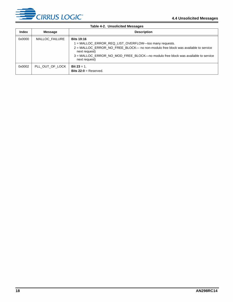
Table 4-2. Unsolicited Messages
Index Message Description
0x0000 MALLOC_FAILURE Bits 19:161 = MALLOC_ERROR_REQ_LIST_OVERFLOW—too many requests.2 = MALLOC_ERROR_NO_FREE_BLOCK— no non-modulo free block was available to service
next request)3 = MALLOC_ERROR_NO_MOD_FREE_BLOCK—no modulo free block was available to service
next request)
0x0002 PLL_OUT_OF_LOCK Bit 23 = 1.Bits 22:0 = Reserved.
18 AN298RC14
5 Audio Manager Firmware Module
5 Audio Manager Firmware Module
5.1 Overview
The Audio Manager Firmware module provides the ability for the microcontroller to easily manage general audio controls such as gain, mute, trim and channel remap.
5.2 Audio Manager
Index = 0xHHHH, data value = 0xhhhhhhhh
Write = 0x8300HHHH 0xhhhhhhhh
Read Request = 0x83c0HHHH
Read Response = 0x03c0HHHH 0xhhhhhhhh
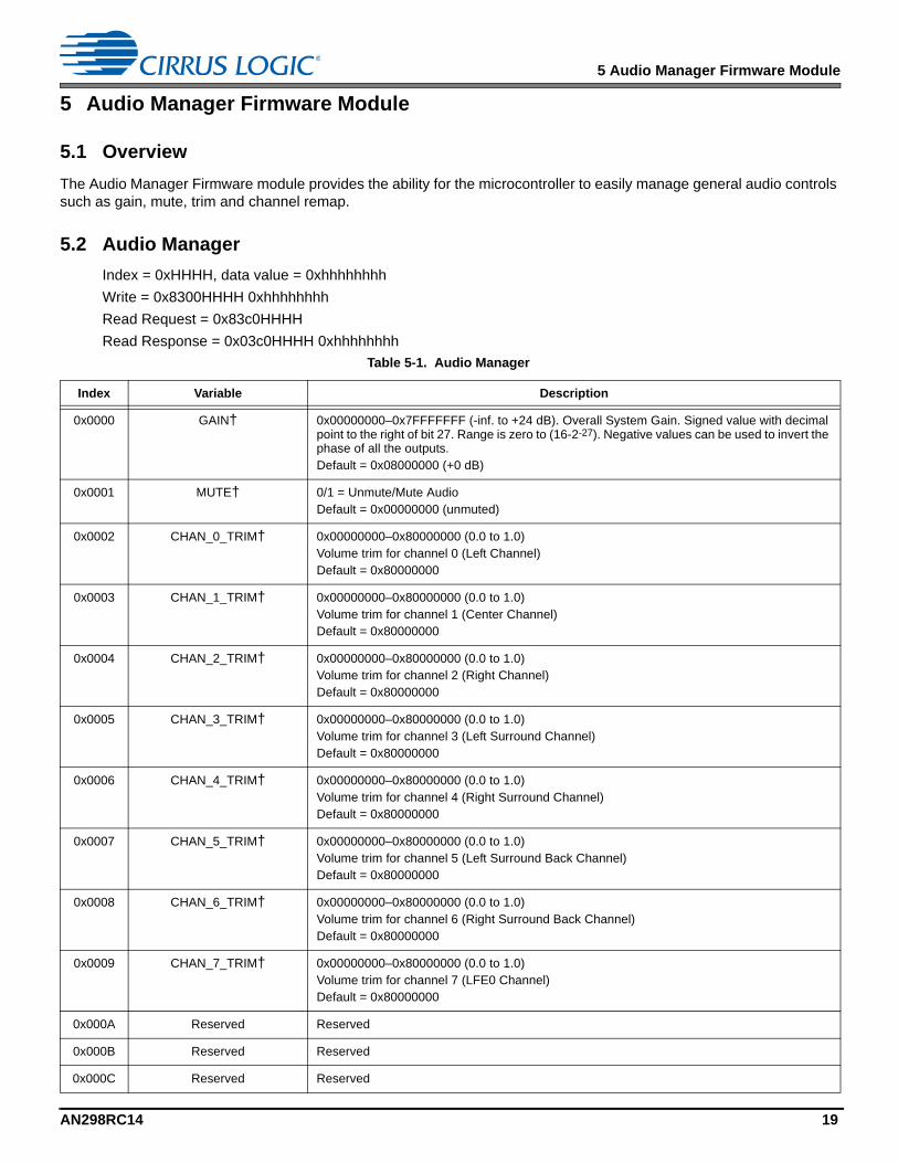
Table 5-1. Audio Manager
Index Variable Description
0x0000 GAIN† 0x00000000–0x7FFFFFFF (-inf. to +24 dB). Overall System Gain. Signed value with decimal point to the right of bit 27. Range is zero to (16-2-27). Negative values can be used to invert the phase of all the outputs.Default = 0x08000000 (+0 dB)
0x0001 MUTE† 0/1 = Unmute/Mute AudioDefault = 0x00000000 (unmuted)
0x0002 CHAN_0_TRIM† 0x00000000–0x80000000 (0.0 to 1.0)Volume trim for channel 0 (Left Channel)Default = 0x80000000
0x0003 CHAN_1_TRIM† 0x00000000–0x80000000 (0.0 to 1.0)Volume trim for channel 1 (Center Channel)Default = 0x80000000
0x0004 CHAN_2_TRIM† 0x00000000–0x80000000 (0.0 to 1.0)Volume trim for channel 2 (Right Channel)Default = 0x80000000
0x0005 CHAN_3_TRIM† 0x00000000–0x80000000 (0.0 to 1.0)Volume trim for channel 3 (Left Surround Channel)Default = 0x80000000
0x0006 CHAN_4_TRIM† 0x00000000–0x80000000 (0.0 to 1.0)Volume trim for channel 4 (Right Surround Channel)Default = 0x80000000
0x0007 CHAN_5_TRIM† 0x00000000–0x80000000 (0.0 to 1.0)Volume trim for channel 5 (Left Surround Back Channel)Default = 0x80000000
0x0008 CHAN_6_TRIM† 0x00000000–0x80000000 (0.0 to 1.0)Volume trim for channel 6 (Right Surround Back Channel)Default = 0x80000000
0x0009 CHAN_7_TRIM† 0x00000000–0x80000000 (0.0 to 1.0)Volume trim for channel 7 (LFE0 Channel)Default = 0x80000000
0x000A Reserved Reserved
0x000B Reserved Reserved
0x000C Reserved Reserved
AN298RC14 19
5.2 Audio Manager
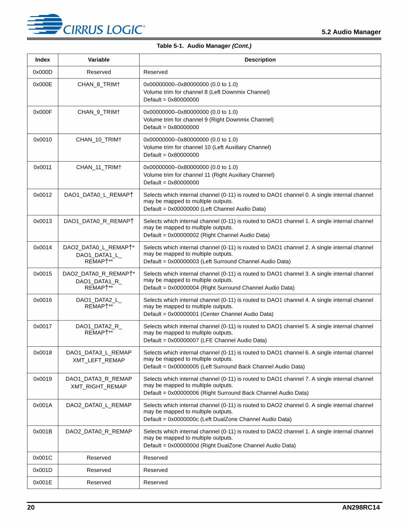
0x000D Reserved Reserved
0x000E CHAN_8_TRIM† 0x00000000–0x80000000 (0.0 to 1.0)Volume trim for channel 8 (Left Downmix Channel)Default = 0x80000000
0x000F CHAN_9_TRIM† 0x00000000–0x80000000 (0.0 to 1.0)Volume trim for channel 9 (Right Downmix Channel)Default = 0x80000000
0x0010 CHAN_10_TRIM† 0x00000000–0x80000000 (0.0 to 1.0)Volume trim for channel 10 (Left Auxiliary Channel)Default = 0x80000000
0x0011 CHAN_11_TRIM† 0x00000000–0x80000000 (0.0 to 1.0)Volume trim for channel 11 (Right Auxiliary Channel)Default = 0x80000000
0x0012 DAO1_DATA0_L_REMAP† Selects which internal channel (0-11) is routed to DAO1 channel 0. A single internal channel may be mapped to multiple outputs.Default = 0x00000000 (Left Channel Audio Data)
0x0013 DAO1_DATA0_R_REMAP† Selects which internal channel (0-11) is routed to DAO1 channel 1. A single internal channel may be mapped to multiple outputs.Default = 0x00000002 (Right Channel Audio Data)
0x0014 DAO2_DATA0_L_REMAP†*DAO1_DATA1_L_
REMAP†**
Selects which internal channel (0-11) is routed to DAO1 channel 2. A single internal channel may be mapped to multiple outputs.Default = 0x00000003 (Left Surround Channel Audio Data)
0x0015 DAO2_DATA0_R_REMAP†*DAO1_DATA1_R_
REMAP†**
Selects which internal channel (0-11) is routed to DAO1 channel 3. A single internal channel may be mapped to multiple outputs.Default = 0x00000004 (Right Surround Channel Audio Data)
0x0016 DAO1_DATA2_L_REMAP†**
Selects which internal channel (0-11) is routed to DAO1 channel 4. A single internal channel may be mapped to multiple outputs.Default = 0x00000001 (Center Channel Audio Data)
0x0017 DAO1_DATA2_R_REMAP†**
Selects which internal channel (0-11) is routed to DAO1 channel 5. A single internal channel may be mapped to multiple outputs.Default = 0x00000007 (LFE Channel Audio Data)
0x0018 DAO1_DATA3_L_REMAPXMT_LEFT_REMAP
Selects which internal channel (0-11) is routed to DAO1 channel 6. A single internal channel may be mapped to multiple outputs.Default = 0x00000005 (Left Surround Back Channel Audio Data)
0x0019 DAO1_DATA3_R_REMAPXMT_RIGHT_REMAP
Selects which internal channel (0-11) is routed to DAO1 channel 7. A single internal channel may be mapped to multiple outputs.Default = 0x00000006 (Right Surround Back Channel Audio Data)
0x001A DAO2_DATA0_L_REMAP Selects which internal channel (0-11) is routed to DAO2 channel 0. A single internal channel may be mapped to multiple outputs.Default = 0x0000000c (Left DualZone Channel Audio Data)
0x001B DAO2_DATA0_R_REMAP Selects which internal channel (0-11) is routed to DAO2 channel 1. A single internal channel may be mapped to multiple outputs.Default = 0x0000000d (Right DualZone Channel Audio Data)
0x001C Reserved Reserved
0x001D Reserved Reserved
0x001E Reserved Reserved
Table 5-1. Audio Manager (Cont.)
Index Variable Description
20 AN298RC14
5.3 Audio Manager in DSP Composer Environment
* This is only available on the CS48520.
** This is only available on the CS48540 and CS48560.
*** This is only available on the CS48560.
5.3 Audio Manager in DSP Composer Environment
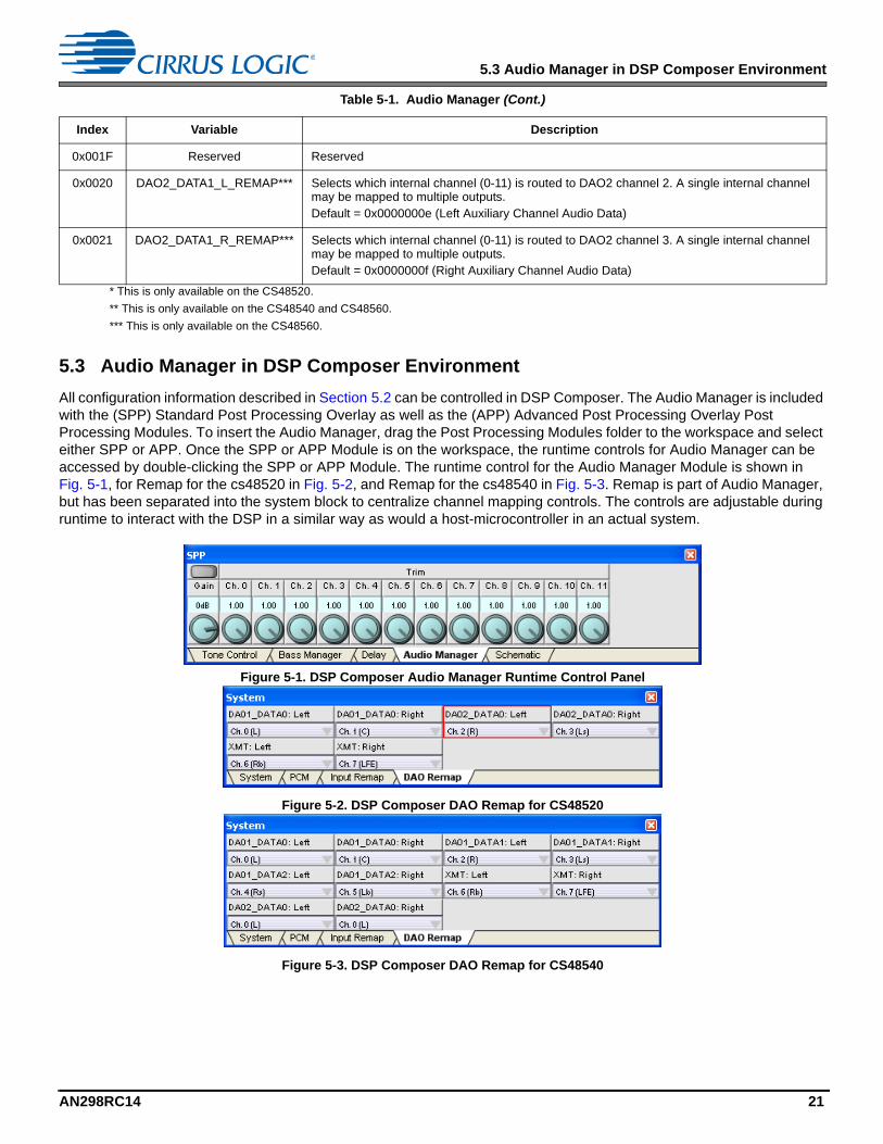
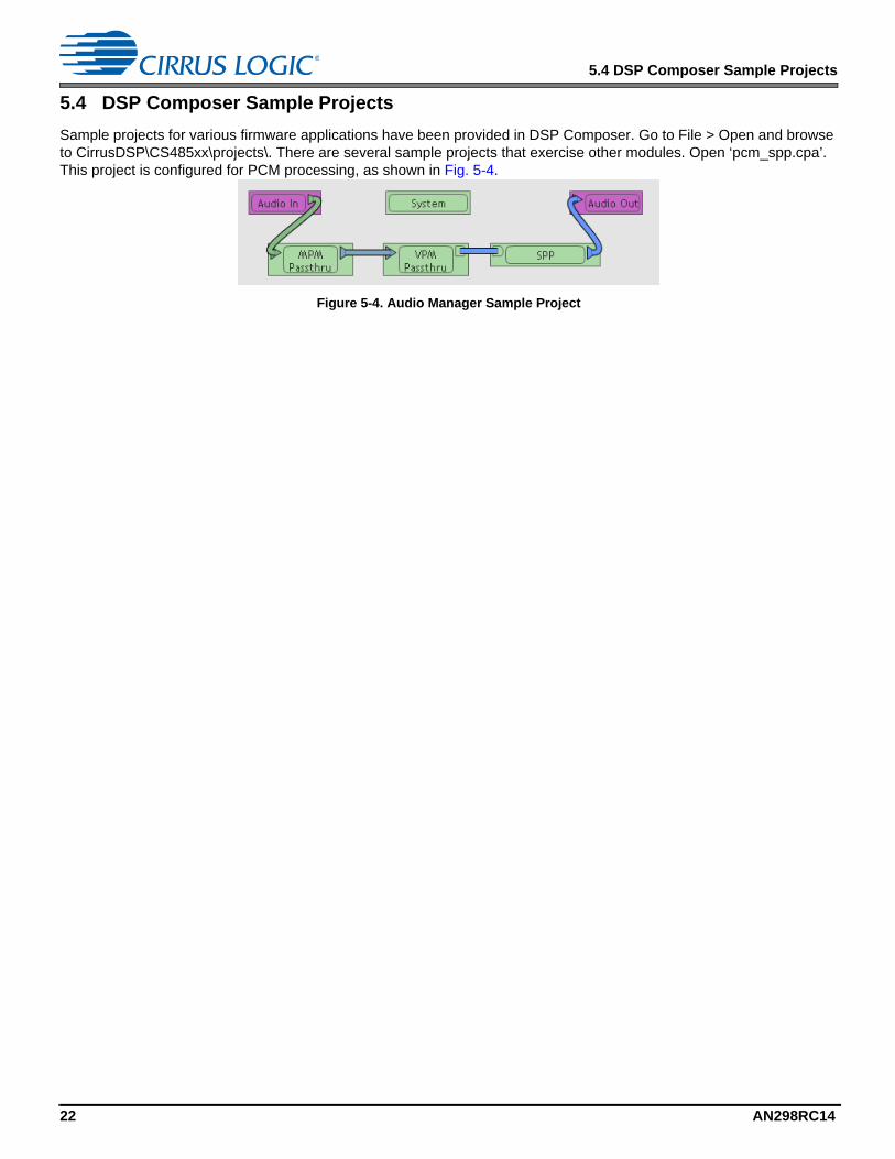
All configuration information described in Section 5.2 can be controlled in DSP Composer. The Audio Manager is included with the (SPP) Standard Post Processing Overlay as well as the (APP) Advanced Post Processing Overlay Post Processing Modules. To insert the Audio Manager, drag the Post Processing Modules folder to the workspace and select either SPP or APP. Once the SPP or APP Module is on the workspace, the runtime controls for Audio Manager can be accessed by double-clicking the SPP or APP Module. The runtime control for the Audio Manager Module is shown in Fig. 5-1, for Remap for the cs48520 in Fig. 5-2, and Remap for the cs48540 in Fig. 5-3. Remap is part of Audio Manager, but has been separated into the system block to centralize channel mapping controls. The controls are adjustable during runtime to interact with the DSP in a similar way as would a host-microcontroller in an actual system.
Figure 5-1. DSP Composer Audio Manager Runtime Control Panel
Figure 5-2. DSP Composer DAO Remap for CS48520
Figure 5-3. DSP Composer DAO Remap for CS48540
0x001F Reserved Reserved
0x0020 DAO2_DATA1_L_REMAP*** Selects which internal channel (0-11) is routed to DAO2 channel 2. A single internal channel may be mapped to multiple outputs.Default = 0x0000000e (Left Auxiliary Channel Audio Data)
0x0021 DAO2_DATA1_R_REMAP*** Selects which internal channel (0-11) is routed to DAO2 channel 3. A single internal channel may be mapped to multiple outputs.Default = 0x0000000f (Right Auxiliary Channel Audio Data)
Table 5-1. Audio Manager (Cont.)
Index Variable Description
AN298RC14 21
5.4 DSP Composer Sample Projects
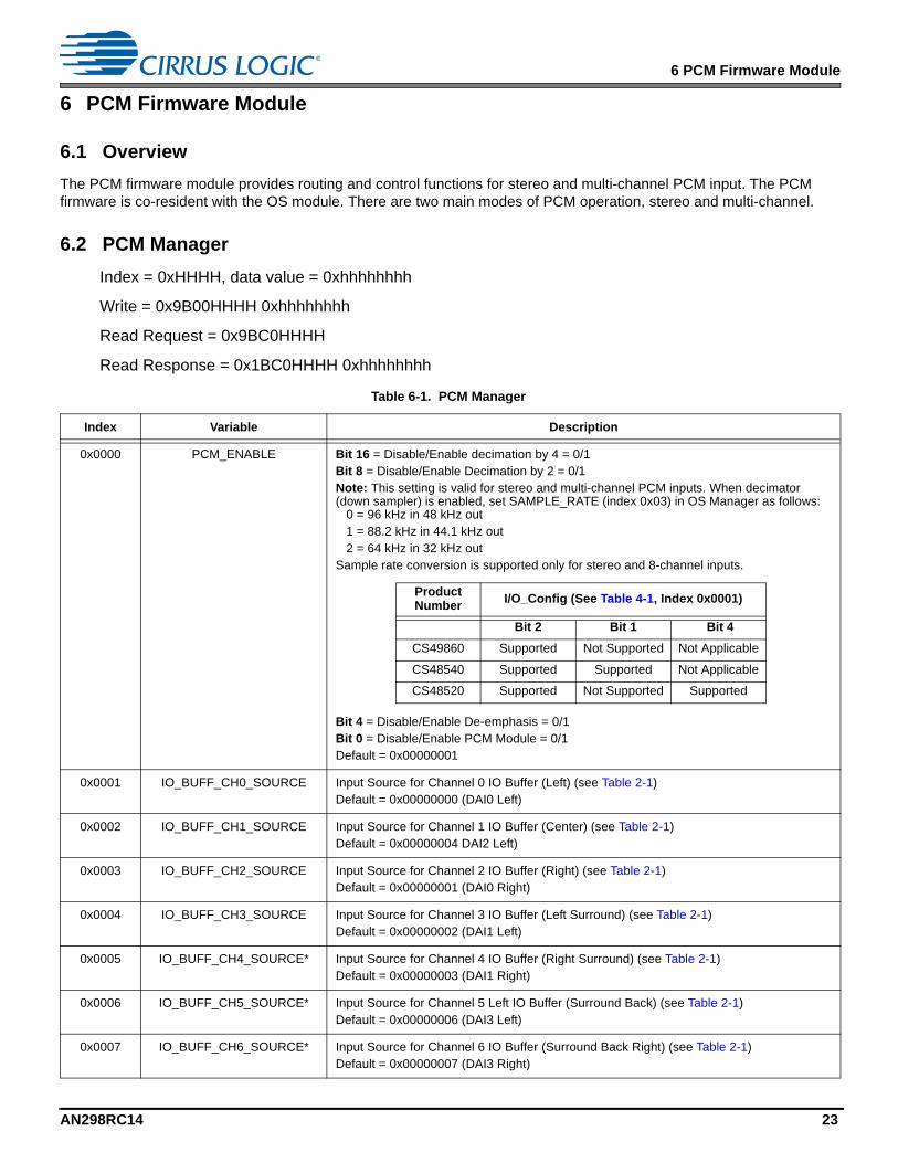
5.4 DSP Composer Sample Projects
Sample projects for various firmware applications have been provided in DSP Composer. Go to File > Open and browse to CirrusDSP\CS485xx\projects\. There are several sample projects that exercise other modules. Open ‘pcm_spp.cpa’. This project is configured for PCM processing, as shown in Fig. 5-4.
Figure 5-4. Audio Manager Sample Project
22 AN298RC14
6 PCM Firmware Module
6 PCM Firmware Module
6.1 Overview
The PCM firmware module provides routing and control functions for stereo and multi-channel PCM input. The PCM firmware is co-resident with the OS module. There are two main modes of PCM operation, stereo and multi-channel.
6.2 PCM Manager
Index = 0xHHHH, data value = 0xhhhhhhhh
Write = 0x9B00HHHH 0xhhhhhhhh
Read Request = 0x9BC0HHHH
Read Response = 0x1BC0HHHH 0xhhhhhhhh
Table 6-1. PCM Manager
Index Variable Description
0x0000 PCM_ENABLE Bit 16 = Disable/Enable decimation by 4 = 0/1Bit 8 = Disable/Enable Decimation by 2 = 0/1Note: This setting is valid for stereo and multi-channel PCM inputs. When decimator (down sampler) is enabled, set SAMPLE_RATE (index 0x03) in OS Manager as follows:
0 = 96 kHz in 48 kHz out1 = 88.2 kHz in 44.1 kHz out2 = 64 kHz in 32 kHz out
Sample rate conversion is supported only for stereo and 8-channel inputs.
Bit 4 = Disable/Enable De-emphasis = 0/1Bit 0 = Disable/Enable PCM Module = 0/1Default = 0x00000001
0x0001 IO_BUFF_CH0_SOURCE Input Source for Channel 0 IO Buffer (Left) (see Table 2-1)Default = 0x00000000 (DAI0 Left)
0x0002 IO_BUFF_CH1_SOURCE Input Source for Channel 1 IO Buffer (Center) (see Table 2-1) Default = 0x00000004 DAI2 Left)
0x0003 IO_BUFF_CH2_SOURCE Input Source for Channel 2 IO Buffer (Right) (see Table 2-1)Default = 0x00000001 (DAI0 Right)
0x0004 IO_BUFF_CH3_SOURCE Input Source for Channel 3 IO Buffer (Left Surround) (see Table 2-1)Default = 0x00000002 (DAI1 Left)
0x0005 IO_BUFF_CH4_SOURCE* Input Source for Channel 4 IO Buffer (Right Surround) (see Table 2-1)Default = 0x00000003 (DAI1 Right)
0x0006 IO_BUFF_CH5_SOURCE* Input Source for Channel 5 Left IO Buffer (Surround Back) (see Table 2-1)Default = 0x00000006 (DAI3 Left)
0x0007 IO_BUFF_CH6_SOURCE* Input Source for Channel 6 IO Buffer (Surround Back Right) (see Table 2-1)Default = 0x00000007 (DAI3 Right)
Product Number
I/O_Config (See Table 4-1, Index 0x0001)
Bit 2 Bit 1 Bit 4
CS49860 Supported Not Supported Not Applicable
CS48540 Supported Supported Not Applicable
CS48520 Supported Not Supported Supported
AN298RC14 23
6.2 PCM Manager
* Not available on the CS48520.
** Not available on the CS48520 and CS48540.
0x0008 IO_BUFF_CH7_SOURCE* Input Source for Channel 7 IO Buffer (LFE0) (see table 2)Default = 0x00000005 (DAI2 Right)
0x0009 IO_BUFF_CH8_SOURCE** Input Source for Channel 8 IO Buffer (Left DualZone) (see table 2)Default = 0x08000000 (no source)
0x000A IO_BUFF_CH9_SOURCE** Input Source for Channel 9 IO Buffer (Right DualZone) (see table 2)Default = 0x08000000 (no source)
0x000B IO_BUFF_CH10_SOURCE** Input Source for Channel 10 IO Buffer (Left Auxiliary) (see table 2)Default = 0x08000000 (no source)
0x000C IO_BUFF_CH11_SOURCE** Input Source for Channel 11 IO Buffer (Right Auxiliary) (see table 2)Default = 0x08000000 (no source)
0x000D Reserved Reserved
0x000E PCM_INPUT_MODE Bit 31: 0/1 Disable/Enable LFE processing thru PCM input Bits 3:0 Input Mode (number of input channels present in the system)
0x0 = 2/0 Lt, Rt Dolby Surround compatible0x1 = 1/0 C0x2 = 2/0 L/R0x3 = 3/0 L/C/R0x4 = 2/1 L/R/S0x5 = 3/1 L/C/R/S0x6 = 2/2 L/R/Ls/Rs0x7 = 3/2 L/C/R/Ls/Rs0x8 = 3/3 L/C/R/Ls/Rs/Cs0x9 = 3/4 L/C/R/Ls/Rs/Sbl/Sbr0xA = 2/3 L/R/Ls/Rs/Cs0xB = 2/4 L/R/Ls/Rs/Sbl/Sbr
Default = 0x00000002
Table 6-1. PCM Manager (Cont.)
Index Variable Description
24 AN298RC14
6.3 PCM Manager in DSP Composer
6.3 PCM Manager in DSP Composer
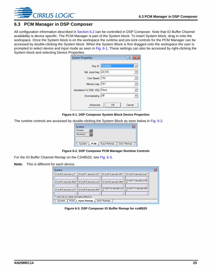
All configuration information described in Section 6.2 can be controlled in DSP Composer. Note that IO Buffer Channel availability is device specific. The PCM Manager is part of the System block. To insert System block, drag in onto the workspace. Once the System block is on the workspace the runtime and pre-kick controls for the PCM Manager can be accessed by double-clicking the System block. When the System Block is first dragged onto the workspace the user is prompted to select device and input mode as seen in Fig. 6-1. These settings can also be accessed by right-clicking the System block and selecting Device Properties.
Figure 6-1. DSP Composer System Block Device Properties
The runtime controls are accessed by double-clicking the System Block as seen below in Fig. 6-2.
Figure 6-2. DSP Composer PCM Manager Runtime Controls
For the IO Buffer Channel Remap on the CS48520, see Fig. 6-3.
Note: This is different for each device.
Figure 6-3. DSP Composer IO Buffer Remap for cs48520
AN298RC14 25
6.4 PCM Module Notes
6.4 PCM Module Notes
The following are the possible PCM input modes:
• Stereo Mode: Stereo PCM into DAI_D4. 2 Channel Mode set in IO_CONFIG in the OS Manager.
• Multi-channel Mode: PCM into DAI_D0 thru DAI_D3. Multi-Channel Mode set in IO_CONFIG in the OS Manager.
Stereo and Multi-channel input modes above are mutually exclusive and must be configured prior to runtime (pre-kick-start). At runtime, switching between modes is not allowed.
Table 6-2. Valid IO_BUFF_*_SOURCE Values
Value Source (multichannel mode)Source
(Stereo mode)
0 DAI1_D0 Left DAI Left
1 DAI1_D0 Right DAI Right
2 DAI1_D1 Left None
3 DAI1_D1 Right None
4 DAI1_D2 Left None
5 DAI1_D2 Right None
6 DAI1_D3 Left None
7 DAI1_D3 Right None
8 DAI1_D4 Left None
9 DAI1_D4 Right None
10 DAI2_D0 Left None
11 DAI2_D0 Right None
0x08000000 None None
26 AN298RC14
7 Low Power Mode
7 Low Power Mode
Note: The Low Power Mode section will be moving to the CS485xx Hardware User’s Manual in the next revision of that manual.
The CS485xx has a low power mode to enable power savings when not in use. Low power mode is entered during the softboot procedure.
7.1 Low Power Mode Messaging
One message is relevant to the low power mode procedure for the CS485xx. This message is SOFTBOOT_LP. The host must read any ACK and prior messages before low power mode may commence.
7.2 Low Power Mode Steps
1. The system controller should send the SOFTBOOT_LP message (0x81000009 0x00000011).
2. The CS485xx is now in low power mode.
3. To test that the CS485xx is in low power mode, the host controller can send a message and verify that there is no response. Additionally all the GPIO pins will be set to inputs in low power mode with weak pull-ups so their state can be checked to verify low power mode is active.
7.3 Getting Out of Low Power Mode
1. Set DSP_RESET low.
2. Set DSP_RESET high.
3. Send the SLAVE_BOOT message (0x80000000).
4. Read the BOOT_START message (0x00000001).
5. Send the WAKEUP_*.ULD file.
Note: This is dependent on the current memory configuration. For example: if loading os_48520_p2_*.uld, then send wakeup_p2.uld. If loading os_48520_p4_*.uld, then send wakeup_p4.uld, and so forth. See Table 7-1.
6. Read the BOOT_SUCCESS message (0x00000002).
7. Send the SOFT_RESET message (0x40000000).
8. Read the APP_START message (0x00000004).
9. Send Hardware Configuration messages.
10.Send Software Configuration messages.
11.Send the KICKSTART message.
Mnemonic Value
SOFTBOOT_LP 0x810000090x00000011
AN298RC14 27
7.3 Getting Out of Low Power Mode
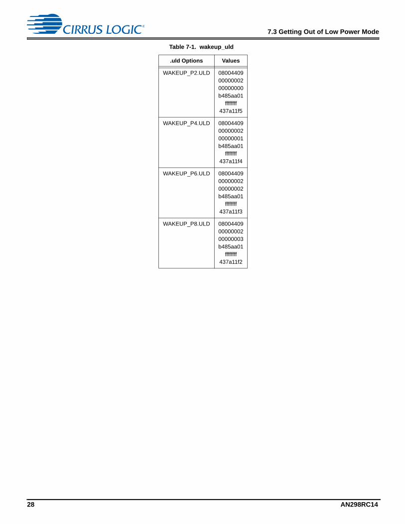
Table 7-1. wakeup_uld
.uld Options Values
WAKEUP_P2.ULD 080044090000000200000000b485aa01
ffffffff437a11f5
WAKEUP_P4.ULD 080044090000000200000001b485aa01
ffffffff437a11f4
WAKEUP_P6.ULD 080044090000000200000002b485aa01
ffffffff437a11f3
WAKEUP_P8.ULD 080044090000000200000003b485aa01
ffffffff437a11f2
28 AN298RC14
8 Watchdog Timer
8 Watchdog Timer
The CS485xx has an integrated hardware watchdog timer that acts as a “health” monitor for the DSP. The watchdog timer must be reset by the DSP before the counter expires, or the entire chip is reset. This peripheral ensures that the CS485xx will reset itself in the event of a temporary system failure. In standalone mode (no host MCU), the DSP will reboot from external FLASH. In slave mode (host MCU present), all GPIOs will be pulled high to signal the host that the watchdog has expired and the DSP should be rebooted and reconfigured. The watchdog timer is disabled upon reset. There are three important registers that the host uses for configuring the watchdog timer. They are KICKSTART, WDG_RELOAD, and WDG_COUNT.
Note: The enabling of the watchdog timer happens post-kick-start.
8.1 Watchdog Timer Messaging
The KICKSTART message is shown below, to enable the watchdog set bit 8 (a = 1). To enable no watchdog re-kicking, set bit 9 as well (a = 3). No watching re-kicking is only used as a test hook to verify that the reset occurs when the timer expires.
The WDG_COUNT message is shown below and reflects the watchdog state at last timer ISR. The default is abcdefgh = FFFFFFFF.
The WDG_RELOAD message is used to set the watchdog reload time and is shown in the table below. The default is abcdefgh = 00BB800, which is a 1 second reload time at 12.288 MHz.
The equation to calculate the watchdog reload time is shown below:
Watchdog reload time = MCLK / WDG_RELOAD
Mnemonic Value
KICKSTART 0x810000000x00000a00
Mnemonic Value
WDG_COUNT 0x810000180xabcdefgh
Mnemonic Value
WDG_RELOAD 0x810000190xabcdefgh
AN298RC14 29
9 Document Revisions
9 Document RevisionsRevision Date Changes
RC1 December, 2006 Initial Release
RC2 September, 2007 Updated KICKSTART and PLL_STANDARD_CONFIG; added PLL_CUSTOM_CONFIG0, PLL_CUSTOM_CONFIG1, and MALLOC_FAILURE.
RC3 December, 2007 Updated Legal Notice. Removed Softboot procedure that was duplicated in Chapter 2 of the CS485xxHardware User’s Manual.
RC4 July, 2008 Updated Table 2-1 with read and write address information for firmware modules listed in that table. Updated implementation status and definitions of GPIO_D, GPIO_OE, and GPIO_MUX variables in Table 4-1. Added DAI_CLOCK_SOURCE variable in Table 4-1.
RC5 October, 2008 Added Bits 20, 21, and 22 to the KICKSTART variable in Table 4-1. Changed product family number from CS485xx to CS48xxxxx, which now covers the CS485xx, CS48AU2B, and CS48DV2B products.
RC6 October, 2008 Added Section 2.2, which describes .uld files. Updated Table 2-1, adding Audyssey Dynamic Volume and Dynamic EQ, Audyssey EQ, and Audyssey EQ firmware modules to the table.
RC7 December, 2008 Modified Section 7.
RC8 August, 2009 Updated Table 2-1. Added Table 2-2. Updated bit definitions for index 0x0001, IO_CONFIG. Updated bit definitions for index 0x0000, PCM_ENABLE.
RC9 September, 2009 Added Cirrus Bass Enhancer to Table 2-1.
RC10 September, 2009 Added “†” symbol for indices 0x0012 to 0x0019 in Table 5-1, indicating that the indices can be modified after kick-start.
RC11 December, 2010 Added definition of Bit 8 to CONTROL_WORD variable in Table 5-1. Added index 0x0052 to Table 4-1.
RC12 November, 2011 Added information regarding PLL out of lock message to Section 3.1.3.
RC13 November, 2012 Updated PCM Manager Controls screenshot in Fig. 6-2.
RC14 March, 2013 Updated Index 0x000a–0x0021 and removed 0x0022 in Table 5-1.
Contacting Cirrus Logic Support For all product questions and inquiries, contact a Cirrus Logic Sales Representative. To find the one nearest you, go to www.cirrus.com.
IMPORTANT NOTICE
Cirrus Logic, Inc. and its subsidiaries (“Cirrus”) believe that the information contained in this document is accurate and reliable. However, the information is subject to changewithout notice and is provided “AS IS” without warranty of any kind (express or implied). Customers are advised to obtain the latest version of relevant information to verify,before placing orders, that information being relied on is current and complete. All products are sold subject to the terms and conditions of sale supplied at the time of orderacknowledgment, including those pertaining to warranty, indemnification, and limitation of liability. No responsibility is assumed by Cirrus for the use of this information,including use of this information as the basis for manufacture or sale of any items, or for infringement of patents or other rights of third parties. This document is the propertyof Cirrus and by furnishing this information, Cirrus grants no license, express or implied under any patents, mask work rights, copyrights, trademarks, trade secrets or otherintellectual property rights. Cirrus owns the copyrights associated with the information contained herein and gives consent for copies to be made of the information only foruse within your organization with respect to Cirrus integrated circuits or other products of Cirrus. This consent does not extend to other copying such as copying for generaldistribution, advertising or promotional purposes, or for creating any work for resale.
CERTAIN APPLICATIONS USING SEMICONDUCTOR PRODUCTS MAY INVOLVE POTENTIAL RISKS OF DEATH, PERSONAL INJURY, OR SEVERE PROPERTY ORENVIRONMENTAL DAMAGE (“CRITICAL APPLICATIONS”). CIRRUS PRODUCTS ARE NOT DESIGNED, AUTHORIZED OR WARRANTED FOR USE IN PRODUCTSSURGICALLY IMPLANTED INTO THE BODY, AUTOMOTIVE SAFETY OR SECURITY DEVICES, LIFE SUPPORT PRODUCTS OR OTHER CRITICAL APPLICATIONS.INCLUSION OF CIRRUS PRODUCTS IN SUCH APPLICATIONS IS UNDERSTOOD TO BE FULLY AT THE CUSTOMER’S RISK AND CIRRUS DISCLAIMS AND MAKESNO WARRANTY, EXPRESS, STATUTORY OR IMPLIED, INCLUDING THE IMPLIED WARRANTIES OF MERCHANTABILITY AND FITNESS FOR PARTICULARPURPOSE, WITH REGARD TO ANY CIRRUS PRODUCT THAT IS USED IN SUCH A MANNER. IF THE CUSTOMER OR CUSTOMER’S CUSTOMER USES OR PERMITSTHE USE OF CIRRUS PRODUCTS IN CRITICAL APPLICATIONS, CUSTOMER AGREES, BY SUCH USE, TO FULLY INDEMNIFY CIRRUS, ITS OFFICERS, DIRECTORS,EMPLOYEES, DISTRIBUTORS AND OTHER AGENTS FROM ANY AND ALL LIABILITY, INCLUDING ATTORNEYS’ FEES AND COSTS, THAT MAY RESULT FROM ORARISE IN CONNECTION WITH THESE USES.
Cirrus Logic, Cirrus, the Cirrus Logic logo designs, DSP Composer, and Intelligent Room Calibration are trademarks of Cirrus Logic, Inc. All other brand and product namesin this document may be trademarks or service marks of their respective owners.
Dolby, the “double-D” logo, Dolby Digital, Audistry, Dolby Headphone, Dolby Virtual Surround, and Pro Logic are registered trademarks of Dolby Laboratories, Inc. AAC is atrademark of Dolby Laboratories, Inc. Supply of an implementation of Dolby Technology does not convey a license nor imply a right under any patent, or any other industrialor Intellectual Property Right of Dolby Laboratories, to use the Implementation in any finished end-user or ready-to-use final product. It is hereby notified that a license forsuch use is required from Dolby Laboratories.
DTS is a registered trademark of the Digital Theater Systems, Inc. DTS NEO:6 is a trademark of Digital Theater Systems, Inc. It is hereby notified that a third-party licensefrom DTS is necessary to distribute software of DTS in any finished end-user or ready-to-use final product.
THX® Technology by Lucasarts Entertainment Company Corporation. THX is a registered trademark of Lucasarts Entertainment Company Corporation.
SRS, Circle Surround, Trusurround, Trusurround XT, and TruBass are registered trademarks of SRS Labs, Inc. Circle Surround, Trusurround, Trusurround XT, and TruBasstechnologies are incorporated under license from SRS Labs, Inc. The Circle Surround, Trusurround, Trusurround XT, and TruBass technology/solution rights incorporated inthe CS485xx are owned by SRS Labs, a U.S. Corporation and licensed to Cirrus Logic, Inc. Purchaser of CS485xx must sign a license for use of the chip and display of theSRS Labs trademarks. Any products incorporating the CS485xx must be sent to SRS Labs for review. SRS Circle Surround, Trusurround, Trusurround XT, and TruBasstechnologies are protected under US and foreign patents issued and/or pending. Circle Surround, Trusurround, Trusurround XT, TruBass, SRS and (O) symbol are trademarksof SRS Labs, Inc. in the United States and selected foreign countries. Neither the purchase of the CS485xx, nor the corresponding sale of audio enhancement equipmentconveys the right to sell commercialized recordings made with any SRS technology/solution. SRS Labs requires all set makers to comply with all rules and regulations asoutlined in the SRS Trademark Usage Manual.
30 AN298RC14