AN2606 Application note - CuVoodoo
194
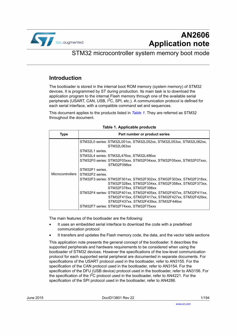
June 2015 DocID13801 Rev 22 1/194 1 AN2606 Application note STM32 microcontroller system memory boot mode Introduction The bootloader is stored in the internal boot ROM memory (system memory) of STM32 devices. It is programmed by ST during production. Its main task is to download the application program to the internal Flash memory through one of the available serial peripherals (USART, CAN, USB, I 2 C, SPI, etc.). A communication protocol is defined for each serial interface, with a compatible command set and sequences. This document applies to the products listed in Table 1. They are referred as STM32 throughout the document. The main features of the bootloader are the following: • It uses an embedded serial interface to download the code with a predefined communication protocol • It transfers and updates the Flash memory code, the data, and the vector table sections This application note presents the general concept of the bootloader. It describes the supported peripherals and hardware requirements to be considered when using the bootloader of STM32 devices. However the specifications of the low-level communication protocol for each supported serial peripheral are documented in separate documents. For specifications of the USART protocol used in the bootloader, refer to AN3155. For the specification of the CAN protocol used in the bootloader, refer to AN3154. For the specification of the DFU (USB device) protocol used in the bootloader, refer to AN3156. For the specification of the I 2 C protocol used in the bootloader, refer to AN4221. For the specification of the SPI protocol used in the bootloader, refer to AN4286. Table 1. Applicable products Type Part number or product series Microcontrollers STM32L0 series: STM32L051xx, STM32L052xx, STM32L053xx, STM32L062xx, STM32L063xx STM32L1 series. STM32L4 series: STM32L476xx, STM32L486xx STM32F0 series: STM32F03xxx, STM32F04xxx, STM32F05xxx, STM32F07xxx, STM32F098xx STM32F1 series. STM32F2 series. STM32F3 series: STM32F301xx, STM32F302xx, STM32F303xx, STM32F318xx, STM32F328xx, STM32F334xx, STM32F358xx, STM32F373xx, STM32F378xx, STM32F398xx STM32F4 series: STM32F401xx, STM32F405xx, STM32F407xx, STM32F411xx, STM32F415xx, STM32F417xx, STM32F427xx, STM32F429xx, STM32F437xx, STM32F439xx, STM32F446xx STM32F7 series: STM32F74xxx, STM32F75xxx www.st.com
Transcript of AN2606 Application note - CuVoodoo
June 2015 DocID13801 Rev 22 1/194
1
AN2606Application note
STM32 microcontroller system memory boot mode
Introduction
The bootloader is stored in the internal boot ROM memory (system memory) of STM32 devices. It is programmed by ST during production. Its main task is to download the application program to the internal Flash memory through one of the available serial peripherals (USART, CAN, USB, I2C, SPI, etc.). A communication protocol is defined for each serial interface, with a compatible command set and sequences.
This document applies to the products listed in Table 1. They are referred as STM32 throughout the document.
The main features of the bootloader are the following:
• It uses an embedded serial interface to download the code with a predefined communication protocol
• It transfers and updates the Flash memory code, the data, and the vector table sections
This application note presents the general concept of the bootloader. It describes the supported peripherals and hardware requirements to be considered when using the bootloader of STM32 devices. However the specifications of the low-level communication protocol for each supported serial peripheral are documented in separate documents. For specifications of the USART protocol used in the bootloader, refer to AN3155. For the specification of the CAN protocol used in the bootloader, refer to AN3154. For the specification of the DFU (USB device) protocol used in the bootloader, refer to AN3156. For the specification of the I2C protocol used in the bootloader, refer to AN4221. For the specification of the SPI protocol used in the bootloader, refer to AN4286.
Table 1. Applicable products
Type Part number or product series
Microcontrollers
STM32L0 series: STM32L051xx, STM32L052xx, STM32L053xx, STM32L062xx, STM32L063xx
STM32L1 series.STM32L4 series: STM32L476xx, STM32L486xxSTM32F0 series: STM32F03xxx, STM32F04xxx, STM32F05xxx, STM32F07xxx,
STM32F098xxSTM32F1 series.STM32F2 series.STM32F3 series: STM32F301xx, STM32F302xx, STM32F303xx, STM32F318xx,
STM32F328xx, STM32F334xx, STM32F358xx, STM32F373xx, STM32F378xx, STM32F398xx
STM32F4 series: STM32F401xx, STM32F405xx, STM32F407xx, STM32F411xx, STM32F415xx, STM32F417xx, STM32F427xx, STM32F429xx, STM32F437xx, STM32F439xx, STM32F446xx
STM32F7 series: STM32F74xxx, STM32F75xxx
www.st.com
Contents AN2606
2/194 DocID13801 Rev 22
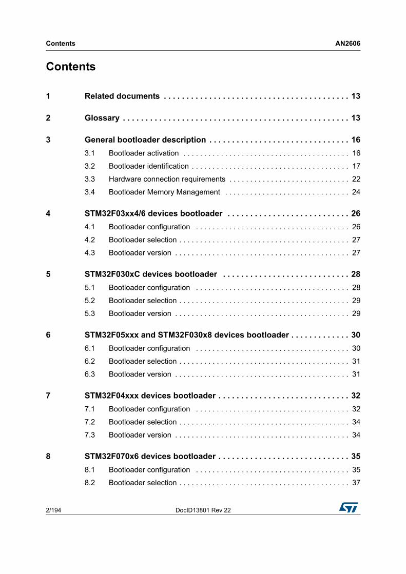
Contents
1 Related documents . . . . . . . . . . . . . . . . . . . . . . . . . . . . . . . . . . . . . . . . . 13
2 Glossary . . . . . . . . . . . . . . . . . . . . . . . . . . . . . . . . . . . . . . . . . . . . . . . . . . 13
3 General bootloader description . . . . . . . . . . . . . . . . . . . . . . . . . . . . . . . 16
3.1 Bootloader activation . . . . . . . . . . . . . . . . . . . . . . . . . . . . . . . . . . . . . . . . 16
3.2 Bootloader identification . . . . . . . . . . . . . . . . . . . . . . . . . . . . . . . . . . . . . . 17
3.3 Hardware connection requirements . . . . . . . . . . . . . . . . . . . . . . . . . . . . . 22
3.4 Bootloader Memory Management . . . . . . . . . . . . . . . . . . . . . . . . . . . . . . 24
4 STM32F03xx4/6 devices bootloader . . . . . . . . . . . . . . . . . . . . . . . . . . . 26
4.1 Bootloader configuration . . . . . . . . . . . . . . . . . . . . . . . . . . . . . . . . . . . . . 26
4.2 Bootloader selection . . . . . . . . . . . . . . . . . . . . . . . . . . . . . . . . . . . . . . . . . 27
4.3 Bootloader version . . . . . . . . . . . . . . . . . . . . . . . . . . . . . . . . . . . . . . . . . . 27
5 STM32F030xC devices bootloader . . . . . . . . . . . . . . . . . . . . . . . . . . . . 28
5.1 Bootloader configuration . . . . . . . . . . . . . . . . . . . . . . . . . . . . . . . . . . . . . 28
5.2 Bootloader selection . . . . . . . . . . . . . . . . . . . . . . . . . . . . . . . . . . . . . . . . . 29
5.3 Bootloader version . . . . . . . . . . . . . . . . . . . . . . . . . . . . . . . . . . . . . . . . . . 29
6 STM32F05xxx and STM32F030x8 devices bootloader . . . . . . . . . . . . . 30
6.1 Bootloader configuration . . . . . . . . . . . . . . . . . . . . . . . . . . . . . . . . . . . . . 30
6.2 Bootloader selection . . . . . . . . . . . . . . . . . . . . . . . . . . . . . . . . . . . . . . . . . 31
6.3 Bootloader version . . . . . . . . . . . . . . . . . . . . . . . . . . . . . . . . . . . . . . . . . . 31
7 STM32F04xxx devices bootloader . . . . . . . . . . . . . . . . . . . . . . . . . . . . . 32
7.1 Bootloader configuration . . . . . . . . . . . . . . . . . . . . . . . . . . . . . . . . . . . . . 32
7.2 Bootloader selection . . . . . . . . . . . . . . . . . . . . . . . . . . . . . . . . . . . . . . . . . 34
7.3 Bootloader version . . . . . . . . . . . . . . . . . . . . . . . . . . . . . . . . . . . . . . . . . . 34
8 STM32F070x6 devices bootloader . . . . . . . . . . . . . . . . . . . . . . . . . . . . . 35
8.1 Bootloader configuration . . . . . . . . . . . . . . . . . . . . . . . . . . . . . . . . . . . . . 35
8.2 Bootloader selection . . . . . . . . . . . . . . . . . . . . . . . . . . . . . . . . . . . . . . . . . 37
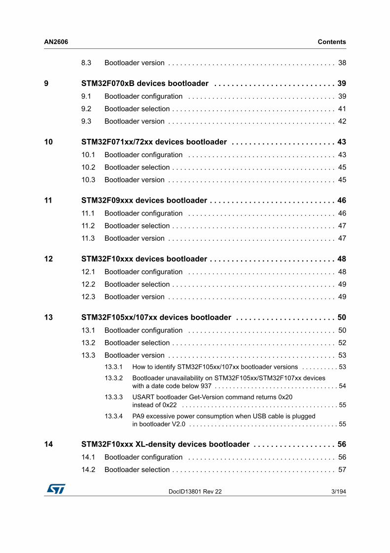
DocID13801 Rev 22 3/194
AN2606 Contents
8
8.3 Bootloader version . . . . . . . . . . . . . . . . . . . . . . . . . . . . . . . . . . . . . . . . . . 38
9 STM32F070xB devices bootloader . . . . . . . . . . . . . . . . . . . . . . . . . . . . 39
9.1 Bootloader configuration . . . . . . . . . . . . . . . . . . . . . . . . . . . . . . . . . . . . . 39
9.2 Bootloader selection . . . . . . . . . . . . . . . . . . . . . . . . . . . . . . . . . . . . . . . . . 41
9.3 Bootloader version . . . . . . . . . . . . . . . . . . . . . . . . . . . . . . . . . . . . . . . . . . 42
10 STM32F071xx/72xx devices bootloader . . . . . . . . . . . . . . . . . . . . . . . . 43
10.1 Bootloader configuration . . . . . . . . . . . . . . . . . . . . . . . . . . . . . . . . . . . . . 43
10.2 Bootloader selection . . . . . . . . . . . . . . . . . . . . . . . . . . . . . . . . . . . . . . . . . 45
10.3 Bootloader version . . . . . . . . . . . . . . . . . . . . . . . . . . . . . . . . . . . . . . . . . . 45
11 STM32F09xxx devices bootloader . . . . . . . . . . . . . . . . . . . . . . . . . . . . . 46
11.1 Bootloader configuration . . . . . . . . . . . . . . . . . . . . . . . . . . . . . . . . . . . . . 46
11.2 Bootloader selection . . . . . . . . . . . . . . . . . . . . . . . . . . . . . . . . . . . . . . . . . 47
11.3 Bootloader version . . . . . . . . . . . . . . . . . . . . . . . . . . . . . . . . . . . . . . . . . . 47
12 STM32F10xxx devices bootloader . . . . . . . . . . . . . . . . . . . . . . . . . . . . . 48
12.1 Bootloader configuration . . . . . . . . . . . . . . . . . . . . . . . . . . . . . . . . . . . . . 48
12.2 Bootloader selection . . . . . . . . . . . . . . . . . . . . . . . . . . . . . . . . . . . . . . . . . 49
12.3 Bootloader version . . . . . . . . . . . . . . . . . . . . . . . . . . . . . . . . . . . . . . . . . . 49
13 STM32F105xx/107xx devices bootloader . . . . . . . . . . . . . . . . . . . . . . . 50
13.1 Bootloader configuration . . . . . . . . . . . . . . . . . . . . . . . . . . . . . . . . . . . . . 50
13.2 Bootloader selection . . . . . . . . . . . . . . . . . . . . . . . . . . . . . . . . . . . . . . . . . 52
13.3 Bootloader version . . . . . . . . . . . . . . . . . . . . . . . . . . . . . . . . . . . . . . . . . . 53
13.3.1 How to identify STM32F105xx/107xx bootloader versions . . . . . . . . . . 53
13.3.2 Bootloader unavailability on STM32F105xx/STM32F107xx devices with a date code below 937 . . . . . . . . . . . . . . . . . . . . . . . . . . . . . . . . . . 54
13.3.3 USART bootloader Get-Version command returns 0x20 instead of 0x22 . . . . . . . . . . . . . . . . . . . . . . . . . . . . . . . . . . . . . . . . . . . 55
13.3.4 PA9 excessive power consumption when USB cable is plugged in bootloader V2.0 . . . . . . . . . . . . . . . . . . . . . . . . . . . . . . . . . . . . . . . . . 55
14 STM32F10xxx XL-density devices bootloader . . . . . . . . . . . . . . . . . . . 56
14.1 Bootloader configuration . . . . . . . . . . . . . . . . . . . . . . . . . . . . . . . . . . . . . 56
14.2 Bootloader selection . . . . . . . . . . . . . . . . . . . . . . . . . . . . . . . . . . . . . . . . . 57

Contents AN2606
4/194 DocID13801 Rev 22
14.3 Bootloader version . . . . . . . . . . . . . . . . . . . . . . . . . . . . . . . . . . . . . . . . . . 57
15 STM32F2xxxx devices bootloader . . . . . . . . . . . . . . . . . . . . . . . . . . . . . 58
15.1 Bootloader V2.x . . . . . . . . . . . . . . . . . . . . . . . . . . . . . . . . . . . . . . . . . . . . 58
15.1.1 Bootloader configuration . . . . . . . . . . . . . . . . . . . . . . . . . . . . . . . . . . . . 58
15.1.2 Bootloader selection . . . . . . . . . . . . . . . . . . . . . . . . . . . . . . . . . . . . . . . 59
15.1.3 Bootloader version . . . . . . . . . . . . . . . . . . . . . . . . . . . . . . . . . . . . . . . . . 60
15.2 Bootloader V3.x . . . . . . . . . . . . . . . . . . . . . . . . . . . . . . . . . . . . . . . . . . . . 61
15.2.1 Bootloader configuration . . . . . . . . . . . . . . . . . . . . . . . . . . . . . . . . . . . . 61
15.2.2 Bootloader selection . . . . . . . . . . . . . . . . . . . . . . . . . . . . . . . . . . . . . . . 63
15.2.3 Bootloader version . . . . . . . . . . . . . . . . . . . . . . . . . . . . . . . . . . . . . . . . . 64
16 STM32F301xx/302x4(6/8) devices bootloader . . . . . . . . . . . . . . . . . . . 65
16.1 Bootloader configuration . . . . . . . . . . . . . . . . . . . . . . . . . . . . . . . . . . . . . 65
16.2 Bootloader selection . . . . . . . . . . . . . . . . . . . . . . . . . . . . . . . . . . . . . . . . . 67
16.3 Bootloader version . . . . . . . . . . . . . . . . . . . . . . . . . . . . . . . . . . . . . . . . . . 67
17 STM32F302xB(C)/303xB(C) devices bootloader . . . . . . . . . . . . . . . . . . 68
17.1 Bootloader configuration . . . . . . . . . . . . . . . . . . . . . . . . . . . . . . . . . . . . . 68
17.2 Bootloader selection . . . . . . . . . . . . . . . . . . . . . . . . . . . . . . . . . . . . . . . . . 70
17.3 Bootloader version . . . . . . . . . . . . . . . . . . . . . . . . . . . . . . . . . . . . . . . . . . 70
18 STM32F302xD(E)/303xD(E) devices bootloader . . . . . . . . . . . . . . . . . . 71
18.1 Bootloader configuration . . . . . . . . . . . . . . . . . . . . . . . . . . . . . . . . . . . . . 71
18.2 Bootloader selection . . . . . . . . . . . . . . . . . . . . . . . . . . . . . . . . . . . . . . . . . 73
18.3 Bootloader version . . . . . . . . . . . . . . . . . . . . . . . . . . . . . . . . . . . . . . . . . . 74
19 STM32F303x4(6/8)/334xx/328xx devices bootloader . . . . . . . . . . . . . . 75
19.1 Bootloader configuration . . . . . . . . . . . . . . . . . . . . . . . . . . . . . . . . . . . . . 75
19.2 Bootloader selection . . . . . . . . . . . . . . . . . . . . . . . . . . . . . . . . . . . . . . . . . 76
19.3 Bootloader version . . . . . . . . . . . . . . . . . . . . . . . . . . . . . . . . . . . . . . . . . . 76
20 STM32F318xx devices bootloader . . . . . . . . . . . . . . . . . . . . . . . . . . . . . 77
20.1 Bootloader configuration . . . . . . . . . . . . . . . . . . . . . . . . . . . . . . . . . . . . . 77
20.2 Bootloader selection . . . . . . . . . . . . . . . . . . . . . . . . . . . . . . . . . . . . . . . . . 78
20.3 Bootloader version . . . . . . . . . . . . . . . . . . . . . . . . . . . . . . . . . . . . . . . . . . 79
DocID13801 Rev 22 5/194
AN2606 Contents
8
21 STM32F358xx devices bootloader . . . . . . . . . . . . . . . . . . . . . . . . . . . . . 80
21.1 Bootloader configuration . . . . . . . . . . . . . . . . . . . . . . . . . . . . . . . . . . . . . 80
21.2 Bootloader selection . . . . . . . . . . . . . . . . . . . . . . . . . . . . . . . . . . . . . . . . . 81
21.3 Bootloader version . . . . . . . . . . . . . . . . . . . . . . . . . . . . . . . . . . . . . . . . . . 81
22 STM32F373xx devices bootloader . . . . . . . . . . . . . . . . . . . . . . . . . . . . . 82
22.1 Bootloader configuration . . . . . . . . . . . . . . . . . . . . . . . . . . . . . . . . . . . . . 82
22.2 Bootloader selection . . . . . . . . . . . . . . . . . . . . . . . . . . . . . . . . . . . . . . . . . 84
22.3 Bootloader version . . . . . . . . . . . . . . . . . . . . . . . . . . . . . . . . . . . . . . . . . . 84
23 STM32F378xx devices bootloader . . . . . . . . . . . . . . . . . . . . . . . . . . . . . 85
23.1 Bootloader configuration . . . . . . . . . . . . . . . . . . . . . . . . . . . . . . . . . . . . . 85
23.2 Bootloader selection . . . . . . . . . . . . . . . . . . . . . . . . . . . . . . . . . . . . . . . . . 86
23.3 Bootloader version . . . . . . . . . . . . . . . . . . . . . . . . . . . . . . . . . . . . . . . . . . 86
24 STM32F398xx devices bootloader . . . . . . . . . . . . . . . . . . . . . . . . . . . . . 87
24.1 Bootloader configuration . . . . . . . . . . . . . . . . . . . . . . . . . . . . . . . . . . . . . 87
24.2 Bootloader selection . . . . . . . . . . . . . . . . . . . . . . . . . . . . . . . . . . . . . . . . . 88
24.3 Bootloader version . . . . . . . . . . . . . . . . . . . . . . . . . . . . . . . . . . . . . . . . . . 88
25 STM32F40xxx/41xxx devices bootloader . . . . . . . . . . . . . . . . . . . . . . . 89
25.1 Bootloader V3.x . . . . . . . . . . . . . . . . . . . . . . . . . . . . . . . . . . . . . . . . . . . . 89
25.1.1 Bootloader configuration . . . . . . . . . . . . . . . . . . . . . . . . . . . . . . . . . . . . 89
25.1.2 Bootloader selection . . . . . . . . . . . . . . . . . . . . . . . . . . . . . . . . . . . . . . . 91
25.1.3 Bootloader version . . . . . . . . . . . . . . . . . . . . . . . . . . . . . . . . . . . . . . . . . 92
26 STM32F401xB(C) devices bootloader . . . . . . . . . . . . . . . . . . . . . . . . . . 93
26.1 Bootloader configuration . . . . . . . . . . . . . . . . . . . . . . . . . . . . . . . . . . . . . 93
26.2 Bootloader selection . . . . . . . . . . . . . . . . . . . . . . . . . . . . . . . . . . . . . . . . . 97
26.3 Bootloader version . . . . . . . . . . . . . . . . . . . . . . . . . . . . . . . . . . . . . . . . . . 98
27 STM32F401xD(E) devices bootloader . . . . . . . . . . . . . . . . . . . . . . . . . . 99
27.1 Bootloader configuration . . . . . . . . . . . . . . . . . . . . . . . . . . . . . . . . . . . . . 99
27.2 Bootloader selection . . . . . . . . . . . . . . . . . . . . . . . . . . . . . . . . . . . . . . . . 102
27.3 Bootloader version . . . . . . . . . . . . . . . . . . . . . . . . . . . . . . . . . . . . . . . . . 103

Contents AN2606
6/194 DocID13801 Rev 22
28 STM32F411xx devices bootloader . . . . . . . . . . . . . . . . . . . . . . . . . . . . 104
28.1 Bootloader configuration . . . . . . . . . . . . . . . . . . . . . . . . . . . . . . . . . . . . 104
28.2 Bootloader selection . . . . . . . . . . . . . . . . . . . . . . . . . . . . . . . . . . . . . . . . 108
28.3 Bootloader version . . . . . . . . . . . . . . . . . . . . . . . . . . . . . . . . . . . . . . . . . 109
29 STM32F42xxx/43xxx devices bootloader . . . . . . . . . . . . . . . . . . . . . . 110
29.1 Bootloader V7.x . . . . . . . . . . . . . . . . . . . . . . . . . . . . . . . . . . . . . . . . . . . .110
29.1.1 Bootloader configuration . . . . . . . . . . . . . . . . . . . . . . . . . . . . . . . . . . . 110
29.1.2 Bootloader selection . . . . . . . . . . . . . . . . . . . . . . . . . . . . . . . . . . . . . . 112
29.1.3 Bootloader version . . . . . . . . . . . . . . . . . . . . . . . . . . . . . . . . . . . . . . . . 114
29.2 Bootloader V9.x . . . . . . . . . . . . . . . . . . . . . . . . . . . . . . . . . . . . . . . . . . . .114
29.2.1 Bootloader configuration . . . . . . . . . . . . . . . . . . . . . . . . . . . . . . . . . . . 114
29.2.2 Bootloader selection . . . . . . . . . . . . . . . . . . . . . . . . . . . . . . . . . . . . . . 119
29.2.3 Bootloader version . . . . . . . . . . . . . . . . . . . . . . . . . . . . . . . . . . . . . . . . 121
30 STM32F446xx devices bootloader . . . . . . . . . . . . . . . . . . . . . . . . . . . . 122
30.1 Bootloader configuration . . . . . . . . . . . . . . . . . . . . . . . . . . . . . . . . . . . . 122
30.2 Bootloader selection . . . . . . . . . . . . . . . . . . . . . . . . . . . . . . . . . . . . . . . . 126
30.3 Bootloader version . . . . . . . . . . . . . . . . . . . . . . . . . . . . . . . . . . . . . . . . . 127
31 STM32F74xxx/75xxx devices bootloader . . . . . . . . . . . . . . . . . . . . . . 128
31.1 Bootloader V7.x . . . . . . . . . . . . . . . . . . . . . . . . . . . . . . . . . . . . . . . . . . . 128
31.1.1 Bootloader configuration . . . . . . . . . . . . . . . . . . . . . . . . . . . . . . . . . . . 128
31.1.2 Bootloader selection . . . . . . . . . . . . . . . . . . . . . . . . . . . . . . . . . . . . . . 131
31.1.3 Bootloader version . . . . . . . . . . . . . . . . . . . . . . . . . . . . . . . . . . . . . . . . 132
31.2 Bootloader V9.x . . . . . . . . . . . . . . . . . . . . . . . . . . . . . . . . . . . . . . . . . . . 133
31.2.1 Bootloader configuration . . . . . . . . . . . . . . . . . . . . . . . . . . . . . . . . . . . 133
31.2.2 Bootloader selection . . . . . . . . . . . . . . . . . . . . . . . . . . . . . . . . . . . . . . 136
31.2.3 Bootloader version . . . . . . . . . . . . . . . . . . . . . . . . . . . . . . . . . . . . . . . . 138
32 STM32L05xxx/06xxx devices bootloader . . . . . . . . . . . . . . . . . . . . . . 139
32.1 Bootloader configuration . . . . . . . . . . . . . . . . . . . . . . . . . . . . . . . . . . . . 139
32.2 Bootloader selection . . . . . . . . . . . . . . . . . . . . . . . . . . . . . . . . . . . . . . . . 141
32.3 Bootloader version . . . . . . . . . . . . . . . . . . . . . . . . . . . . . . . . . . . . . . . . . 141
33 STM32L1xxx6(8/B)A devices bootloader . . . . . . . . . . . . . . . . . . . . . . 142
DocID13801 Rev 22 7/194
AN2606 Contents
8
33.1 Bootloader configuration . . . . . . . . . . . . . . . . . . . . . . . . . . . . . . . . . . . . 142
33.2 Bootloader selection . . . . . . . . . . . . . . . . . . . . . . . . . . . . . . . . . . . . . . . . 143
33.3 Bootloader version . . . . . . . . . . . . . . . . . . . . . . . . . . . . . . . . . . . . . . . . . 143
34 STM32L1xxx6(8/B) devices bootloader . . . . . . . . . . . . . . . . . . . . . . . . 144
34.1 Bootloader configuration . . . . . . . . . . . . . . . . . . . . . . . . . . . . . . . . . . . . 144
34.2 Bootloader selection . . . . . . . . . . . . . . . . . . . . . . . . . . . . . . . . . . . . . . . . 145
34.3 Bootloader version . . . . . . . . . . . . . . . . . . . . . . . . . . . . . . . . . . . . . . . . . 145
35 STM32L1xxxC devices bootloader . . . . . . . . . . . . . . . . . . . . . . . . . . . 146
35.1 Bootloader configuration . . . . . . . . . . . . . . . . . . . . . . . . . . . . . . . . . . . . 146
35.2 Bootloader selection . . . . . . . . . . . . . . . . . . . . . . . . . . . . . . . . . . . . . . . . 148
35.3 Bootloader version . . . . . . . . . . . . . . . . . . . . . . . . . . . . . . . . . . . . . . . . . 148
36 STM32L1xxxD devices bootloader . . . . . . . . . . . . . . . . . . . . . . . . . . . 149
36.1 Bootloader configuration . . . . . . . . . . . . . . . . . . . . . . . . . . . . . . . . . . . . 149
36.2 Bootloader selection . . . . . . . . . . . . . . . . . . . . . . . . . . . . . . . . . . . . . . . . 151
36.3 Bootloader version . . . . . . . . . . . . . . . . . . . . . . . . . . . . . . . . . . . . . . . . . 152
36.4 Bootloader V9.x . . . . . . . . . . . . . . . . . . . . . . . . . . . . . . . . . . . . . . . . . . . 153
36.4.1 Bootloader configuration . . . . . . . . . . . . . . . . . . . . . . . . . . . . . . . . . . . 153
36.4.2 Bootloader selection . . . . . . . . . . . . . . . . . . . . . . . . . . . . . . . . . . . . . . 157
36.4.3 Bootloader version . . . . . . . . . . . . . . . . . . . . . . . . . . . . . . . . . . . . . . . . 158
37 STM32L1xxxE devices bootloader . . . . . . . . . . . . . . . . . . . . . . . . . . . 159
37.1 Bootloader configuration . . . . . . . . . . . . . . . . . . . . . . . . . . . . . . . . . . . . 159
37.2 Bootloader selection . . . . . . . . . . . . . . . . . . . . . . . . . . . . . . . . . . . . . . . . 161
37.3 Bootloader version . . . . . . . . . . . . . . . . . . . . . . . . . . . . . . . . . . . . . . . . . 162
38 STM32L476xx/486xx devices bootloader . . . . . . . . . . . . . . . . . . . . . . 163
38.1 Bootloader V10.x . . . . . . . . . . . . . . . . . . . . . . . . . . . . . . . . . . . . . . . . . . 163
38.1.1 Bootloader configuration . . . . . . . . . . . . . . . . . . . . . . . . . . . . . . . . . . . 163
38.1.2 Bootloader selection . . . . . . . . . . . . . . . . . . . . . . . . . . . . . . . . . . . . . . 166
38.1.3 Bootloader version . . . . . . . . . . . . . . . . . . . . . . . . . . . . . . . . . . . . . . . . 168
38.2 Bootloader V9.x . . . . . . . . . . . . . . . . . . . . . . . . . . . . . . . . . . . . . . . . . . . 169
38.2.1 Bootloader configuration . . . . . . . . . . . . . . . . . . . . . . . . . . . . . . . . . . . 169
38.2.2 Bootloader selection . . . . . . . . . . . . . . . . . . . . . . . . . . . . . . . . . . . . . . 172
Contents AN2606
8/194 DocID13801 Rev 22
38.2.3 Bootloader version . . . . . . . . . . . . . . . . . . . . . . . . . . . . . . . . . . . . . . . . 174
39 Device-dependent bootloader parameters . . . . . . . . . . . . . . . . . . . . . 175
40 Bootloader timing . . . . . . . . . . . . . . . . . . . . . . . . . . . . . . . . . . . . . . . . . 177
40.1 Bootloader Startup timing . . . . . . . . . . . . . . . . . . . . . . . . . . . . . . . . . . . . 177
40.2 USART connection timing . . . . . . . . . . . . . . . . . . . . . . . . . . . . . . . . . . . 180
40.3 USB connection timing . . . . . . . . . . . . . . . . . . . . . . . . . . . . . . . . . . . . . . 182
40.4 I2C connection timing . . . . . . . . . . . . . . . . . . . . . . . . . . . . . . . . . . . . . . . 184
40.5 SPI connection timing . . . . . . . . . . . . . . . . . . . . . . . . . . . . . . . . . . . . . . . 186
41 Revision history . . . . . . . . . . . . . . . . . . . . . . . . . . . . . . . . . . . . . . . . . . 187
DocID13801 Rev 22 9/194
AN2606 List of tables
10
List of tables
Table 1. Applicable products . . . . . . . . . . . . . . . . . . . . . . . . . . . . . . . . . . . . . . . . . . . . . . . . . . . . . . . 1Table 2. Bootloader activation patterns . . . . . . . . . . . . . . . . . . . . . . . . . . . . . . . . . . . . . . . . . . . . . . 16Table 3. Embedded bootloaders. . . . . . . . . . . . . . . . . . . . . . . . . . . . . . . . . . . . . . . . . . . . . . . . . . . . 18Table 4. STM32 F2, F4 and F7 Voltage Range configuration using bootloader. . . . . . . . . . . . . . . . 25Table 5. Supported memory area by Write, Read, Erase and Go Commands. . . . . . . . . . . . . . . . . 25Table 6. STM32F03xx4/6 configuration in system memory boot mode . . . . . . . . . . . . . . . . . . . . . . 26Table 7. STM32F03xx4/6 bootloader versions . . . . . . . . . . . . . . . . . . . . . . . . . . . . . . . . . . . . . . . . . 27Table 8. STM32F030xC configuration in system memory boot mode . . . . . . . . . . . . . . . . . . . . . . . 28Table 9. STM32F030xC bootloader versions . . . . . . . . . . . . . . . . . . . . . . . . . . . . . . . . . . . . . . . . . . 29Table 10. STM32F05xxx and STM32F030x8 devices configuration in system memory boot mode . 30Table 11. STM32F05xxx and STM32F030x8 devices bootloader versions . . . . . . . . . . . . . . . . . . . . 31Table 12. STM32F04xxx configuration in system memory boot mode. . . . . . . . . . . . . . . . . . . . . . . . 32Table 13. STM32F04xxx bootloader versions . . . . . . . . . . . . . . . . . . . . . . . . . . . . . . . . . . . . . . . . . . 34Table 14. STM32F070x6 configuration in system memory boot mode. . . . . . . . . . . . . . . . . . . . . . . . 35Table 15. STM32F070x6 bootloader versions . . . . . . . . . . . . . . . . . . . . . . . . . . . . . . . . . . . . . . . . . . 38Table 16. STM32F070xB configuration in system memory boot mode . . . . . . . . . . . . . . . . . . . . . . . 39Table 17. STM32F070xB bootloader versions . . . . . . . . . . . . . . . . . . . . . . . . . . . . . . . . . . . . . . . . . . 42Table 18. STM32F071xx/72xx configuration in system memory boot mode . . . . . . . . . . . . . . . . . . . 43Table 19. STM32F071xx/72xx bootloader versions . . . . . . . . . . . . . . . . . . . . . . . . . . . . . . . . . . . . . . 45Table 20. STM32F09xxx configuration in system memory boot mode. . . . . . . . . . . . . . . . . . . . . . . . 46Table 21. STM32F09xxx bootloader versions . . . . . . . . . . . . . . . . . . . . . . . . . . . . . . . . . . . . . . . . . . 47Table 22. STM32F10xxx configuration in system memory boot mode. . . . . . . . . . . . . . . . . . . . . . . . 48Table 23. STM32F10xxx bootloader versions . . . . . . . . . . . . . . . . . . . . . . . . . . . . . . . . . . . . . . . . . . 49Table 24. STM32F105xx/107xx configuration in system memory boot mode . . . . . . . . . . . . . . . . . . 50Table 25. STM32F105xx/107xx bootloader versions . . . . . . . . . . . . . . . . . . . . . . . . . . . . . . . . . . . . . 53Table 26. STM32F10xxx XL-density configuration in system memory boot mode. . . . . . . . . . . . . . . 56Table 27. STM32F10xxx XL-density bootloader versions . . . . . . . . . . . . . . . . . . . . . . . . . . . . . . . . . 57Table 28. STM32F2xxxx configuration in system memory boot mode . . . . . . . . . . . . . . . . . . . . . . . . 58Table 29. STM32F2xxxx bootloader V2.x versions . . . . . . . . . . . . . . . . . . . . . . . . . . . . . . . . . . . . . . 60Table 30. STM32F2xxxx configuration in system memory boot mode . . . . . . . . . . . . . . . . . . . . . . . . 61Table 31. STM32F2xxxx bootloader V3.x versions . . . . . . . . . . . . . . . . . . . . . . . . . . . . . . . . . . . . . . 64Table 32. STM32F301xx/302x4(6/8) configuration in system memory boot mode. . . . . . . . . . . . . . . 65Table 33. STM32F301xx/302x4(6/8) bootloader versions . . . . . . . . . . . . . . . . . . . . . . . . . . . . . . . . . 67Table 34. STM32F302xB(C)/303xB(C) configuration in system memory boot mode. . . . . . . . . . . . . 68Table 35. STM32F302xB(C)/303xB(C) bootloader versions . . . . . . . . . . . . . . . . . . . . . . . . . . . . . . . 70Table 36. STM32F302xD(E)/303xD(E) configuration in system memory boot mode. . . . . . . . . . . . . 71Table 37. STM32F302xD(E)/303xD(E) bootloader versions . . . . . . . . . . . . . . . . . . . . . . . . . . . . . . . 74Table 38. STM32F303x4(6/8)/334xx/328xx configuration in system memory boot mode . . . . . . . . . 75Table 39. STM32F303x4(6/8)/334xx/328xx bootloader versions . . . . . . . . . . . . . . . . . . . . . . . . . . . . 76Table 40. STM32F318xx configuration in system memory boot mode. . . . . . . . . . . . . . . . . . . . . . . . 77Table 41. STM32F318xx bootloader versions . . . . . . . . . . . . . . . . . . . . . . . . . . . . . . . . . . . . . . . . . . 79Table 42. STM32F358xx configuration in system memory boot mode. . . . . . . . . . . . . . . . . . . . . . . . 80Table 43. STM32F358xx bootloader versions . . . . . . . . . . . . . . . . . . . . . . . . . . . . . . . . . . . . . . . . . . 81Table 44. STM32F373xx configuration in system memory boot mode. . . . . . . . . . . . . . . . . . . . . . . . 82Table 45. STM32F373xx bootloader versions . . . . . . . . . . . . . . . . . . . . . . . . . . . . . . . . . . . . . . . . . . 84Table 46. STM32F378xx configuration in system memory boot mode. . . . . . . . . . . . . . . . . . . . . . . . 85Table 47. STM32F378xx bootloader versions . . . . . . . . . . . . . . . . . . . . . . . . . . . . . . . . . . . . . . . . . . 86Table 48. STM32F398xx configuration in system memory boot mode. . . . . . . . . . . . . . . . . . . . . . . . 87

List of tables AN2606
10/194 DocID13801 Rev 22
Table 49. STM32F398xx bootloader versions . . . . . . . . . . . . . . . . . . . . . . . . . . . . . . . . . . . . . . . . . . 88Table 50. STM32F40xxx/41xxx configuration in system memory boot mode. . . . . . . . . . . . . . . . . . . 89Table 51. STM32F40xxx/41xxx bootloader V3.x versions . . . . . . . . . . . . . . . . . . . . . . . . . . . . . . . . . 92Table 52. STM32F401xB(C) configuration in system memory boot mode . . . . . . . . . . . . . . . . . . . . . 93Table 53. STM32F401xB(C) bootloader versions . . . . . . . . . . . . . . . . . . . . . . . . . . . . . . . . . . . . . . . 98Table 54. STM32F401xD(E) configuration in system memory boot mode . . . . . . . . . . . . . . . . . . . . . 99Table 55. STM32F401xD(E) bootloader versions . . . . . . . . . . . . . . . . . . . . . . . . . . . . . . . . . . . . . . 103Table 56. STM32F411xx configuration in system memory boot mode. . . . . . . . . . . . . . . . . . . . . . . 104Table 57. STM32F411xx bootloader versions . . . . . . . . . . . . . . . . . . . . . . . . . . . . . . . . . . . . . . . . . 109Table 58. STM32F42xxx/43xxx configuration in system memory boot mode. . . . . . . . . . . . . . . . . . 110Table 59. STM32F42xxx/43xxx bootloader V7.x versions . . . . . . . . . . . . . . . . . . . . . . . . . . . . . . . . 114Table 60. STM32F42xxx/43xxx configuration in system memory boot mode. . . . . . . . . . . . . . . . . . 115Table 61. STM32F42xxx/43xxx bootloader V9.x versions . . . . . . . . . . . . . . . . . . . . . . . . . . . . . . . . 121Table 62. STM32F446xx configuration in system memory boot mode. . . . . . . . . . . . . . . . . . . . . . . 122Table 63. STM32F446xx bootloader V9.x versions . . . . . . . . . . . . . . . . . . . . . . . . . . . . . . . . . . . . . 127Table 64. STM32F74xxx/75xxx configuration in system memory boot mode. . . . . . . . . . . . . . . . . . 128Table 65. STM32F74xxx/75xxx bootloader V7.x versions . . . . . . . . . . . . . . . . . . . . . . . . . . . . . . . . 132Table 66. STM32F74xxx/75xxx configuration in system memory boot mode. . . . . . . . . . . . . . . . . . 133Table 67. STM32F74xxx/75xxx bootloader V9.x versions . . . . . . . . . . . . . . . . . . . . . . . . . . . . . . . . 138Table 68. STM32L05xxx/06xxx configuration in system memory boot mode. . . . . . . . . . . . . . . . . . 139Table 69. STM32L05xxx/06xxx bootloader versions . . . . . . . . . . . . . . . . . . . . . . . . . . . . . . . . . . . . 141Table 70. STM32L1xxx6(8/B)A configuration in system memory boot mode. . . . . . . . . . . . . . . . . . 142Table 71. STM32L1xxx6(8/B)A bootloader versions . . . . . . . . . . . . . . . . . . . . . . . . . . . . . . . . . . . . 143Table 72. STM32L1xxx6(8/B) configuration in system memory boot mode . . . . . . . . . . . . . . . . . . . 144Table 73. STM32L1xxx6(8/B) bootloader versions. . . . . . . . . . . . . . . . . . . . . . . . . . . . . . . . . . . . . . 145Table 74. STM32L1xxxC configuration in system memory boot mode. . . . . . . . . . . . . . . . . . . . . . . 146Table 75. STM32L1xxxC bootloader versions . . . . . . . . . . . . . . . . . . . . . . . . . . . . . . . . . . . . . . . . . 148Table 76. STM32L1xxxD configuration in system memory boot mode. . . . . . . . . . . . . . . . . . . . . . . 149Table 77. STM32L1xxxD bootloader versions . . . . . . . . . . . . . . . . . . . . . . . . . . . . . . . . . . . . . . . . . 152Table 78. STM32F40xxx/41xxx configuration in system memory boot mode. . . . . . . . . . . . . . . . . . 153Table 79. STM32F40xxx/41xxx bootloader V9.x versions . . . . . . . . . . . . . . . . . . . . . . . . . . . . . . . . 158Table 80. STM32L1xxxE configuration in system memory boot mode. . . . . . . . . . . . . . . . . . . . . . . 159Table 81. STM32L1xxxE bootloader versions . . . . . . . . . . . . . . . . . . . . . . . . . . . . . . . . . . . . . . . . . 162Table 82. STM32L476xx/486xx configuration in system memory boot mode . . . . . . . . . . . . . . . . . 163Table 83. STM32L476xx/486xx bootloader V10.x versions . . . . . . . . . . . . . . . . . . . . . . . . . . . . . . . 168Table 84. STM32L476xx/486xx configuration in system memory boot mode . . . . . . . . . . . . . . . . . 169Table 85. STM32L476xx/486xx bootloader V9.x versions . . . . . . . . . . . . . . . . . . . . . . . . . . . . . . . . 174Table 86. Bootloader device-dependent parameters . . . . . . . . . . . . . . . . . . . . . . . . . . . . . . . . . . . . 175Table 87. Bootloader startup timings of STM32 devices . . . . . . . . . . . . . . . . . . . . . . . . . . . . . . . . . 177Table 88. USART bootloader minimum timings of STM32 devices . . . . . . . . . . . . . . . . . . . . . . . . . 180Table 89. USB bootloader minimum timings of STM32 devices. . . . . . . . . . . . . . . . . . . . . . . . . . . . 182Table 90. I2C bootloader minimum timings of STM32 devices. . . . . . . . . . . . . . . . . . . . . . . . . . . . . 184Table 91. SPI bootloader minimum timings of STM32 devices . . . . . . . . . . . . . . . . . . . . . . . . . . . . 186Table 92. Document revision history . . . . . . . . . . . . . . . . . . . . . . . . . . . . . . . . . . . . . . . . . . . . . . . . 187
DocID13801 Rev 22 11/194
AN2606 List of figures
12
List of figures
Figure 1. USART Connection . . . . . . . . . . . . . . . . . . . . . . . . . . . . . . . . . . . . . . . . . . . . . . . . . . . . . . 22Figure 2. USB Connection . . . . . . . . . . . . . . . . . . . . . . . . . . . . . . . . . . . . . . . . . . . . . . . . . . . . . . . . . 22Figure 3. I2C Connection . . . . . . . . . . . . . . . . . . . . . . . . . . . . . . . . . . . . . . . . . . . . . . . . . . . . . . . . . . 23Figure 4. SPI Connection. . . . . . . . . . . . . . . . . . . . . . . . . . . . . . . . . . . . . . . . . . . . . . . . . . . . . . . . . . 23Figure 5. CAN Connection . . . . . . . . . . . . . . . . . . . . . . . . . . . . . . . . . . . . . . . . . . . . . . . . . . . . . . . . . 24Figure 6. Bootloader selection for STM32F03xx4/6 devices . . . . . . . . . . . . . . . . . . . . . . . . . . . . . . . 27Figure 7. Bootloader selection for STM32F030xC. . . . . . . . . . . . . . . . . . . . . . . . . . . . . . . . . . . . . . . 29Figure 8. Bootloader selection for STM32F05xxx and STM32F030x8 devices . . . . . . . . . . . . . . . . . 31Figure 9. Bootloader selection for STM32F04xxx . . . . . . . . . . . . . . . . . . . . . . . . . . . . . . . . . . . . . . . 34Figure 10. Bootloader selection for STM32F070x6 . . . . . . . . . . . . . . . . . . . . . . . . . . . . . . . . . . . . . . . 37Figure 11. Bootloader selection for STM32F070xB . . . . . . . . . . . . . . . . . . . . . . . . . . . . . . . . . . . . . . . 41Figure 12. Bootloader selection for STM32F071xx/72xx . . . . . . . . . . . . . . . . . . . . . . . . . . . . . . . . . . . 45Figure 13. Bootloader selection for STM32F09xxx . . . . . . . . . . . . . . . . . . . . . . . . . . . . . . . . . . . . . . . 47Figure 14. Bootloader for STM32F10xxx with USART1 . . . . . . . . . . . . . . . . . . . . . . . . . . . . . . . . . . . 49Figure 15. Bootloader selection for STM32F105xx/107xx devices . . . . . . . . . . . . . . . . . . . . . . . . . . . 52Figure 16. Bootloader selection for STM32F10xxx XL-density devices. . . . . . . . . . . . . . . . . . . . . . . . 57Figure 17. Bootloader V2.x selection for STM32F2xxxx devices. . . . . . . . . . . . . . . . . . . . . . . . . . . . . 59Figure 18. Bootloader V3.x selection for STM32F2xxxx devices. . . . . . . . . . . . . . . . . . . . . . . . . . . . . 63Figure 19. Bootloader selection for STM32F301xx/302x4(6/8) . . . . . . . . . . . . . . . . . . . . . . . . . . . . . . 67Figure 20. Bootloader selection for STM32F302xB(C)/303xB(C) devices. . . . . . . . . . . . . . . . . . . . . . 70Figure 21. Bootloader selection for STM32F302xD(E)/303xD(E) . . . . . . . . . . . . . . . . . . . . . . . . . . . . 73Figure 22. Bootloader selection for STM32F303x4(6/8)/334xx/328xx. . . . . . . . . . . . . . . . . . . . . . . . . 76Figure 23. Bootloader selection for STM32F318xx . . . . . . . . . . . . . . . . . . . . . . . . . . . . . . . . . . . . . . . 78Figure 24. Bootloader selection for STM32F358xx devices . . . . . . . . . . . . . . . . . . . . . . . . . . . . . . . . 81Figure 25. Bootloader selection for STM32F373xx devices . . . . . . . . . . . . . . . . . . . . . . . . . . . . . . . . 84Figure 26. Bootloader selection for STM32F378xx devices . . . . . . . . . . . . . . . . . . . . . . . . . . . . . . . . 86Figure 27. Bootloader selection for STM32F398xx . . . . . . . . . . . . . . . . . . . . . . . . . . . . . . . . . . . . . . . 88Figure 28. Bootloader V3.x selection for STM32F40xxx/41xxx devices . . . . . . . . . . . . . . . . . . . . . . . 91Figure 29. Bootloader selection for STM32F401xB(C) . . . . . . . . . . . . . . . . . . . . . . . . . . . . . . . . . . . . 97Figure 30. Bootloader selection for STM32F401xD(E) . . . . . . . . . . . . . . . . . . . . . . . . . . . . . . . . . . . 102Figure 31. Bootloader selection for STM32F411xx . . . . . . . . . . . . . . . . . . . . . . . . . . . . . . . . . . . . . . 108Figure 32. Dual Bank Boot Implementation for STM32F42xxx/43xxx Bootloader V7.x . . . . . . . . . . . 112Figure 33. Bootloader V7.x selection for STM32F42xxx/43xxx . . . . . . . . . . . . . . . . . . . . . . . . . . . . . 113Figure 34. Dual Bank Boot Implementation for STM32F42xxx/43xxx Bootloader V9.x . . . . . . . . . . . 119Figure 35. Bootloader V9.x selection for STM32F42xxx/43xxx . . . . . . . . . . . . . . . . . . . . . . . . . . . . . 120Figure 36. Bootloader V9.x selection for STM32F446xx . . . . . . . . . . . . . . . . . . . . . . . . . . . . . . . . . . 126Figure 37. Bootloader V7.x selection for STM32F74xxx/75xxx . . . . . . . . . . . . . . . . . . . . . . . . . . . . . 131Figure 38. Bootloader V9.x selection for STM32F74xxx/75xxx . . . . . . . . . . . . . . . . . . . . . . . . . . . . . 137Figure 39. Bootloader selection for STM32L05xxx/06xxx . . . . . . . . . . . . . . . . . . . . . . . . . . . . . . . . . 141Figure 40. Bootloader selection for STM32L1xxx6(8/B)A devices. . . . . . . . . . . . . . . . . . . . . . . . . . . 143Figure 41. Bootloader selection for STM32L1xxx6(8/B) devices . . . . . . . . . . . . . . . . . . . . . . . . . . . . 145Figure 42. Bootloader selection for STM32L1xxxC devices . . . . . . . . . . . . . . . . . . . . . . . . . . . . . . . 148Figure 43. Bootloader selection for STM32L1xxxD devices . . . . . . . . . . . . . . . . . . . . . . . . . . . . . . . 151Figure 44. Bootloader V9.x selection for STM32F40xxx/41xxx . . . . . . . . . . . . . . . . . . . . . . . . . . . . . 157Figure 45. Bootloader selection for STM32L1xxxE devices . . . . . . . . . . . . . . . . . . . . . . . . . . . . . . . 161Figure 46. Dual Bank Boot Implementation for STM32L476xx/486xx Bootloader v10.x . . . . . . . . . . 166Figure 47. Bootloader V10.x selection for STM32L476xx/486xx . . . . . . . . . . . . . . . . . . . . . . . . . . . . 167Figure 48. Dual Bank Boot Implementation for STM32L476xx/486xx Bootloader v9.x . . . . . . . . . . . 172
List of figures AN2606
12/194 DocID13801 Rev 22
Figure 49. Bootloader V9.x selection for STM32L476xx/486xx . . . . . . . . . . . . . . . . . . . . . . . . . . . . . 173Figure 50. Bootloader Startup timing description. . . . . . . . . . . . . . . . . . . . . . . . . . . . . . . . . . . . . . . . 177Figure 51. USART connection timing description . . . . . . . . . . . . . . . . . . . . . . . . . . . . . . . . . . . . . . . 180Figure 52. USB connection timing description . . . . . . . . . . . . . . . . . . . . . . . . . . . . . . . . . . . . . . . . . . 182Figure 53. I2C connection timing description. . . . . . . . . . . . . . . . . . . . . . . . . . . . . . . . . . . . . . . . . . . 184Figure 54. SPI connection timing description. . . . . . . . . . . . . . . . . . . . . . . . . . . . . . . . . . . . . . . . . . . 186

DocID13801 Rev 22 13/194
AN2606 Related documents
193
1 Related documents
For each supported product (listed in Table 1), please refer to the following documents available from www.st.com:
• Datasheet or databrief
• Reference manual
2 Glossary
F0 Series:
STM32F03xxx is used to refer to STM32F030x4, STM32F030x6, STM32F038x6, STM32F030xC, STM32F031x4 and STM32F031x6 devices.
STM32F04xxx is used to refer to STM32F042x4 and STM32F042x6 devices.
STM32F05xxx and STM32F030x8 devices is used to refer to STM32F051x4, STM32F051x6, STM32F051x8, STM32F058x8 and STM32F030x8 devices.
STM32F07xxx is used to refer to STM32F070x6, STM32F070xB, STM32F071xB STM32F072x8 and STM32F072xB devices.
STM32F09xxx is used to refer to STM32F091xx and STM32F098xx devices.
F1 Series:
STM32F10xxx is used to refer to Low-density, Medium-density, High-density, Low-density value line, Medium-density value line and High-density value line devices:
Low-density devices are STM32F101xx, STM32F102xx and STM32F103xx microcontrollers where the Flash memory density ranges between 16 and 32 Kbytes.
Medium-density devices are STM32F101xx, STM32F102xx and STM32F103xx microcontrollers where the Flash memory density ranges between 64 and 128 Kbytes.
High-density devices are STM32F101xx and STM32F103xx microcontrollers where the Flash memory density ranges between 256 and 512 Kbytes.
Low-density value line devices are STM32F100xx microcontrollers where the Flash memory density ranges between 16 and 32 Kbytes.
Medium-density value line devices are STM32F100xx microcontrollers where the Flash memory density ranges between 64 and 128 Kbytes.
High-density value line devices are STM32F100xx microcontrollers where the Flash memory density ranges between 256 and 5128 Kbytes.
STM32F105xx/107xx is used to refer to STM32F105xx and STM32F107xx devices.
STM32F10xxx XL-density is used to refer to STM32F101xx and STM32F103xx devices where the Flash memory density ranges between 768 Kbytes and 1 Mbyte.
F2 Series:
STM32F2xxxx is used to refer to STM32F215xx, STM32F205xx, STM32F207xx and SMT32F217xx devices.

Glossary AN2606
14/194 DocID13801 Rev 22
F3 Series:
STM32F301xx/302x4(6/8) is used to refer to STM32F301x4, STM32F301x6, STM32F301x8, STM32F302x4, STM32F302x6 and STM32F302x8 devices.
STM32F302xB(C)/303xB(C) is used to refer to STM32F302xB, STM32F302xC, STM32F303xB and STM32F303xC devices.
STM32F302xD(E)/303xD(E) is used to refer to STM32F302xD, STM32F302xE, STM32F303xD and STM32F303xE devices.
STM32F303x4(6/8)/334xx/328xx is used to refer to STM32F303x4, STM32F303x6, STM32F303x8, STM32F334x4, STM32F334x6, STM32F334x8, and STM32F328x8 devices.
STM32F318xx is used to refer to STM32F318x8 devices.
STM32F358xx is used to refer to STM32F358xC devices.
STM32F373xx is used to refer to STM32F373x8, STM32F373xB and STM32F373xC devices.
STM32F378xx is used to refer to STM32F378xC devices.
STM32F398xx is used to refer to STM32F398xE devices.
F4 Series:
STM32F40xxx/41xxx is used to refer to STM32F405xx, STM32F407xx, STM32F415xx and SMT32F417xx devices.
STM32F401xB(C) is used to refer to STM32F401xB and STM32F401xC devices.
STM32F401xD(E) is used to refer to STM32F401xD and STM32F401xE devices.
STM32F411xx is used to refer to STM32F411xD and STM32F411xE devices.
STM32F42xxx/43xxx is used to refer to STM32F427xx, STM32F429xx, STM32F437xx and STM32F439xx devices
STM32F446xx is used to refer to STM32F446xE and STM32F446xC devices
F7 Series:
STM32F74xxx/75xxx is used to refer to STM32F745xx and STM32F746xx and STM32F756xx devices.
L0 Series:
STM32L05xxx/06xxx is used to refer to STM32L051xx, STM32L052xx, STM32L053xx, STM32L062xx and STM32L063xx ultralow power devices.
L1 Series:
STM32L1xxx6(8/B) is used to refer to STM32L1xxV6T6, STM32L1xxV6H6, STM32L1xxR6T6, STM32L1xxR6H6, STM32L1xxC6T6, STM32L1xxC6H6, STM32L1xxV8T6, STM32L1xxV8H6, STM32L1xxR8T6, STM32L1xxR8H6, STM32L1xxC8T6, STM32L1xxC8H6, STM32L1xxVBT6, STM32L1xxVBH6, STM32L1xxRBT6, STM32L1xxRBH6, STM32L1xxCBT6 and STM32L1xxCBH6 ultralow power devices.
STM32L1xxx6(8/B)A is used to refer to STM32L1xxV6T6-A, STM32L1xxV6H6-A, STM32L1xxR6T6-A, STM32L1xxR6H6-A, STM32L1xxC6T6-A, STM32L1xxC6H6-A, STM32L1xxV8T6-A, STM32L1xxV8H6-A, STM32L1xxR8T6-A, STM32L1xxR8H6-A, STM32L1xxC8T6-A, STM32L1xxC8H6-A, STM32L1xxVBT6-A, STM32L1xxVBH6-A,
DocID13801 Rev 22 15/194
AN2606 Glossary
193
STM32L1xxRBT6-A, STM32L1xxRBH6-A, STM32L1xxCBT6-A and STM32L1xxCBH6-A ultralow power devices.
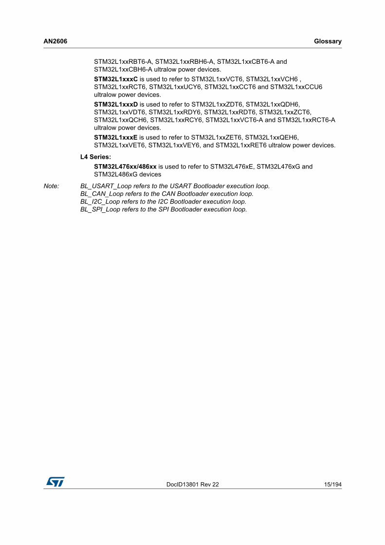
STM32L1xxxC is used to refer to STM32L1xxVCT6, STM32L1xxVCH6 , STM32L1xxRCT6, STM32L1xxUCY6, STM32L1xxCCT6 and STM32L1xxCCU6 ultralow power devices.
STM32L1xxxD is used to refer to STM32L1xxZDT6, STM32L1xxQDH6, STM32L1xxVDT6, STM32L1xxRDY6, STM32L1xxRDT6, STM32L1xxZCT6, STM32L1xxQCH6, STM32L1xxRCY6, STM32L1xxVCT6-A and STM32L1xxRCT6-A ultralow power devices.
STM32L1xxxE is used to refer to STM32L1xxZET6, STM32L1xxQEH6, STM32L1xxVET6, STM32L1xxVEY6, and STM32L1xxRET6 ultralow power devices.
L4 Series:
STM32L476xx/486xx is used to refer to STM32L476xE, STM32L476xG and STM32L486xG devices
Note: BL_USART_Loop refers to the USART Bootloader execution loop. BL_CAN_Loop refers to the CAN Bootloader execution loop. BL_I2C_Loop refers to the I2C Bootloader execution loop. BL_SPI_Loop refers to the SPI Bootloader execution loop.

General bootloader description AN2606
16/194 DocID13801 Rev 22
3 General bootloader description
3.1 Bootloader activation
The bootloader is activated by applying one of the patterns described in Table 2.
If Boot From Bank2 option is activated (for products supporting this feature), Bootloader executes Dual Boot mechanism as described in figures "Dual Bank Boot Implementation for STM32xxxx" where STM32xxxx is the relative STM32 product.
Otherwise, Bootloader selection protocol is executed as described in figures "Bootloader VY.x selection for STM32xxxx" where STM32xxxx is the relative STM32 product.
When readout protection Level2 is activated, STM32 does not boot on system memory in any case and Bootloader can't be executed (unless jumping to it from Flash user code).
Table 2. Bootloader activation patterns
Patterns Condition
Pattern1 Boot0(Pin) = 1 and Boot1(Pin) = 0
Pattern2 Boot0(Pin) = 1 and nBoot1(bit) = 1
Pattern3
Boot0 (Pin)= 1, Boot1(Pin) = 0 and BFB2 (bit) = 1
Boot0(Pin) = 0, BFB2 (bit) = 0 and both banks don’t contain valid code
Boot0(Pin) = 1, Boot1(Pin) = 0, BFB2 (bit) = 0 and both banks don’t contain valid code
Pattern4
Boot0 (Pin)= 1, Boot1(Pin) = 0 and BFB2 (bit) = 1
Boot0(Pin) = 0, BFB2 (bit) = 0 and both banks don’t contain valid code
Boot0(Pin) = 1, Boot1(Pin) = 0 and BFB2 (bit) = 0
Pattern5
Boot0 (Pin)= 1, Boot1(Pin) = 0 and BFB2 (bit) = 0
Boot0(Pin) = 0, BFB2 (bit) = 1 and both banks don’t contain valid code
Boot0(Pin) = 1, Boot1(Pin) = 0 and BFB2 (bit) = 1
Pattern6
Boot0(Pin) = 1, nBoot1(bit) = 1 and nBoot0_SW(bit) = 1
nBoot0(bit) = 0, nBoot1(bit) = 1 and nBoot0_SW(bit) = 0
Boot0(Pin) = 0, nBoot0_SW(bit) = 1 and main flash empty
Pattern7
Boot0 (Pin)= 1, nBoot1(bit) = 1 and BFB2 (bit) = 0
Boot0(Pin) = 0, BFB2 (bit) = 1 and both banks don’t contain valid code
Boot0(Pin) = 1, nBoot1(bit) = 1 and BFB2 (bit) = 1
Pattern8Boot(Pin) = 0 and BOOT_ADD0(optionbyte) = 0x0040
Boot(Pin) = 1 and BOOT_ADD1(optionbyte) = 0x0040

DocID13801 Rev 22 17/194
AN2606 General bootloader description
193
In addition to patterns described above, user can execute bootloader by performing a jump to system memory from user code. Before jumping to Bootloader user must:
• Disable all peripheral clocks
• Disable used PLL
• Disable interrupts
• Clear pending interrupts
System memory boot mode can be exited by getting out from bootloader activation condition and generating hardware reset or using Go command to execute user code.
Note: If you choose to execute the Go command, the peripheral registers used by the bootloader are not initialized to their default reset values before jumping to the user application. They should be reconfigured in the user application if they are used. So, if the IWDG is being used in the application, the IWDG prescaler value has to be adapted to meet the requirements of the application (since the prescaler was set to its maximum value).
3.2 Bootloader identification
Depending on the STM32 device used, the bootloader may support one or more embedded serial peripherals used to download the code to the internal Flash memory. The bootloader identifier (ID) provides information about the supported serial peripherals.
For a given STM32 device, the bootloader is identified by means of the:
1. Bootloader (protocol) version: version of the serial peripheral (USART, CAN, USB, etc.) communication protocol used in the bootloader. This version can be retrieved using the bootloader Get Version command.
2. Bootloader identifier (ID): version of the STM32 device bootloader, coded on one byte in the 0xXY format, where:
– X specifies the embedded serial peripheral(s) used by the device bootloader: X = 1: one USART is used X = 2: two USARTs are used X = 3: USART, CAN and DFU are used X = 4: USART and DFU are used X = 5: USART and I2C are used X = 6: I2C is used X = 7: USART, CAN, DFU and I2C are used X = 8: I2C and SPI are used X = 9: USART, CAN, DFU, I2C and SPI are used X = 10: USART, DFU and I2C are used X = 11: USART, I2C and SPI are used X = 12: USART and SPI are used X = 13: USART, DFU, I2C and SPI are used
– Y specifies the device bootloader version Let us take the example of a bootloader ID equal to 0x10. This means that it is the first version of the device bootloader that uses only one USART. The bootloader ID is programmed in the last byte address - 1 of the device system memory and can be read by using the bootloader “Read memory” command or by direct access to the system memory via JTAG/SWD.
The table below provides identification information about the bootloaders embedded in STM32 devices.

General bootloader description AN2606
18/194 DocID13801 Rev 22
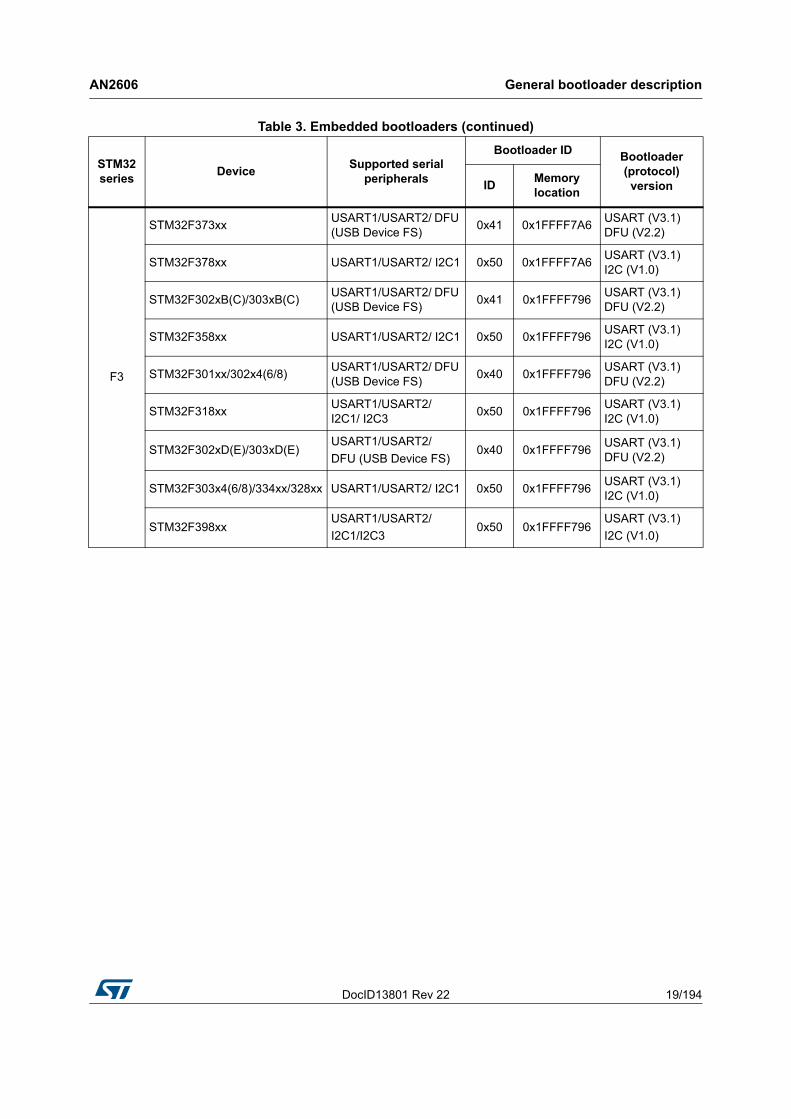
Table 3. Embedded bootloaders
STM32 series
DeviceSupported serial
peripherals
Bootloader ID Bootloader (protocol) versionID
Memory location
F0
STM32F05xxx and STM32F030x8 devices
USART1/USART2 0x21 0x1FFFF7A6 USART (V3.1)
STM32F030xx4/6 USART1 0x10 0x1FFFF7A6 USART (V3.1)
STM32F030xC USART1/I2C1 0x52 0x1FFFF6A6USART (V3.1) I2C1(V1.0)
STM32F04xxxUSART1/USART2/ I2C1/ DFU (USB Device FS)
0xA0 0x1FFFF6A6USART (V3.1) DFU (V2.2) I2C (V1.0)
STM32F071xx/72xxUSART1/USART2/ I2C1/ DFU (USB Device FS)
0xA1 0x1FFFF6A6USART (V3.1) DFU (V2.2) I2C (V1.0)
STM32F070x6USART1/USART2/ DFU (USB Device FS)/
I2C10xA2 0x1FFFF6A6
USART (V3.1)
DFU (V2.2)
I2C (V1.0)
STM32F070xBUSART1/USART2/ DFU (USB Device FS)/
I2C10xA2 0x1FFFF6A6
USART (V3.1)
DFU (V2.2)
I2C (V1.0)
STM32F09xxx USART1/USART2/ I2C1 0x50 0x1FFFF6A6USART (V3.1)
I2C (V1.0)
F1
STM32F10xxx
Low-density USART1 NA NA USART (V2.2)
Medium-density
USART1 NA NA USART (V2.2)
High-density USART1 NA NA USART (V2.2)
Medium-density value line
USART1 0x10 0x1FFFF7D6 USART (V2.2)
High-density value line
USART1 0x10 0x1FFFF7D6 USART (V2.2)
STM32F105xx/107xx
USART1 / USART2 (remapped) / CAN2 (remapped) / DFU (USB Device)
NA NAUSART (V2.2(1)) CAN (V2.0) DFU(V2.2)
STM32F10xxx XL-densityUSART1/USART2 (remapped)
0x21 0x1FFFF7D6 USART (V3.0)
F2 STM32F2xxxx
USART1/USART3 0x20 0x1FFF77DE USART (V3.0)
USART1/USART3/ CAN2/ DFU (USB Device FS)
0x33 0x1FFF77DEUSART (V3.1) CAN (V2.0) DFU (V2.2)
DocID13801 Rev 22 19/194
AN2606 General bootloader description
193
F3
STM32F373xxUSART1/USART2/ DFU (USB Device FS)
0x41 0x1FFFF7A6USART (V3.1) DFU (V2.2)
STM32F378xx USART1/USART2/ I2C1 0x50 0x1FFFF7A6USART (V3.1) I2C (V1.0)
STM32F302xB(C)/303xB(C)USART1/USART2/ DFU (USB Device FS)
0x41 0x1FFFF796USART (V3.1) DFU (V2.2)
STM32F358xx USART1/USART2/ I2C1 0x50 0x1FFFF796USART (V3.1) I2C (V1.0)
STM32F301xx/302x4(6/8)USART1/USART2/ DFU (USB Device FS)
0x40 0x1FFFF796USART (V3.1) DFU (V2.2)
STM32F318xxUSART1/USART2/ I2C1/ I2C3
0x50 0x1FFFF796USART (V3.1) I2C (V1.0)
STM32F302xD(E)/303xD(E)USART1/USART2/
DFU (USB Device FS)0x40 0x1FFFF796
USART (V3.1) DFU (V2.2)
STM32F303x4(6/8)/334xx/328xx USART1/USART2/ I2C1 0x50 0x1FFFF796USART (V3.1) I2C (V1.0)
STM32F398xxUSART1/USART2/
I2C1/I2C30x50 0x1FFFF796
USART (V3.1)
I2C (V1.0)
Table 3. Embedded bootloaders (continued)
STM32 series
DeviceSupported serial
peripherals
Bootloader ID Bootloader (protocol) versionID
Memory location
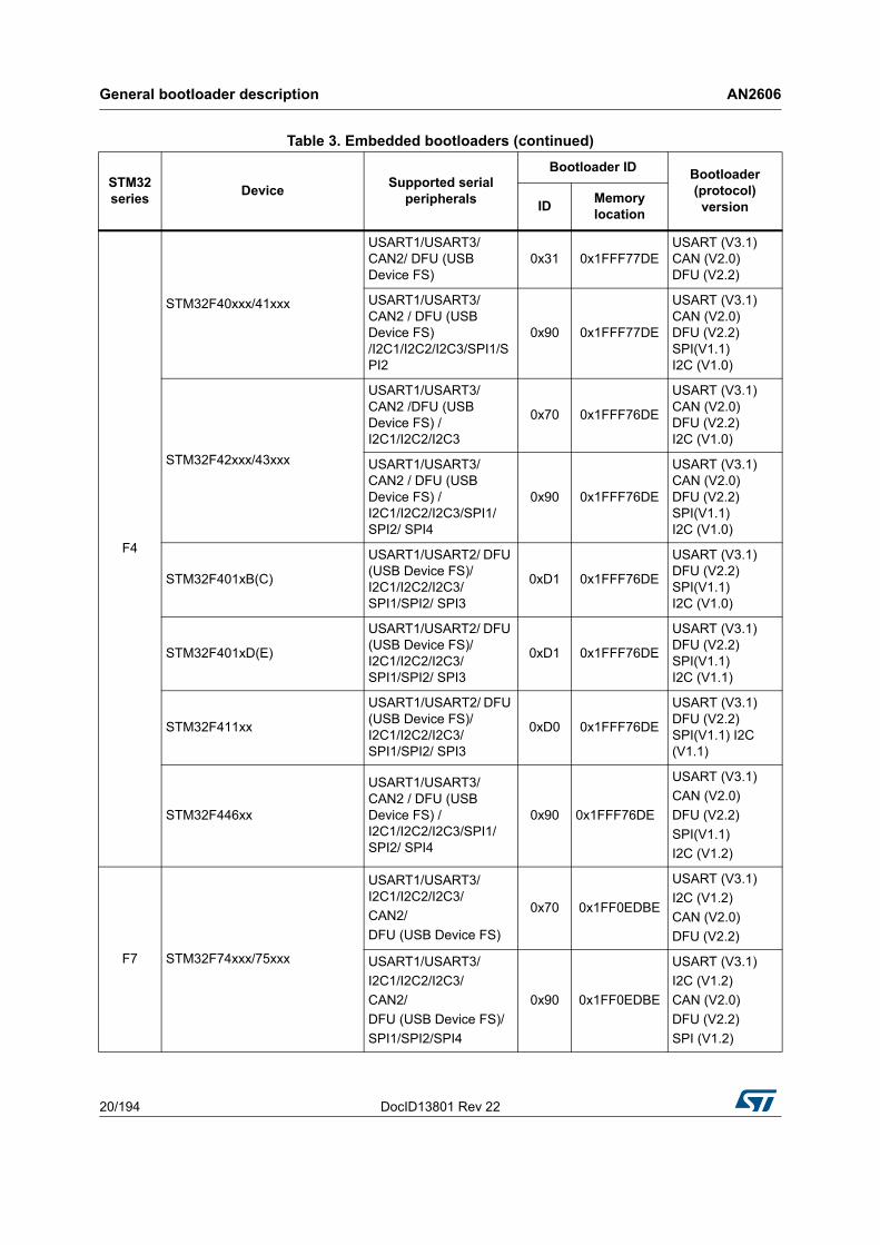
General bootloader description AN2606
20/194 DocID13801 Rev 22
F4
STM32F40xxx/41xxx
USART1/USART3/ CAN2/ DFU (USB Device FS)
0x31 0x1FFF77DEUSART (V3.1) CAN (V2.0) DFU (V2.2)
USART1/USART3/ CAN2 / DFU (USB Device FS) /I2C1/I2C2/I2C3/SPI1/SPI2
0x90 0x1FFF77DE
USART (V3.1) CAN (V2.0) DFU (V2.2) SPI(V1.1) I2C (V1.0)
STM32F42xxx/43xxx
USART1/USART3/ CAN2 /DFU (USB Device FS) / I2C1/I2C2/I2C3
0x70 0x1FFF76DE
USART (V3.1) CAN (V2.0) DFU (V2.2) I2C (V1.0)
USART1/USART3/ CAN2 / DFU (USB Device FS) / I2C1/I2C2/I2C3/SPI1/ SPI2/ SPI4
0x90 0x1FFF76DE
USART (V3.1) CAN (V2.0) DFU (V2.2) SPI(V1.1) I2C (V1.0)
STM32F401xB(C)
USART1/USART2/ DFU (USB Device FS)/ I2C1/I2C2/I2C3/ SPI1/SPI2/ SPI3
0xD1 0x1FFF76DE
USART (V3.1) DFU (V2.2) SPI(V1.1) I2C (V1.0)
STM32F401xD(E)
USART1/USART2/ DFU (USB Device FS)/ I2C1/I2C2/I2C3/ SPI1/SPI2/ SPI3
0xD1 0x1FFF76DE
USART (V3.1) DFU (V2.2) SPI(V1.1) I2C (V1.1)
STM32F411xx
USART1/USART2/ DFU (USB Device FS)/ I2C1/I2C2/I2C3/ SPI1/SPI2/ SPI3
0xD0 0x1FFF76DE
USART (V3.1) DFU (V2.2) SPI(V1.1) I2C (V1.1)
STM32F446xx
USART1/USART3/ CAN2 / DFU (USB Device FS) / I2C1/I2C2/I2C3/SPI1/ SPI2/ SPI4
0x90 0x1FFF76DE
USART (V3.1)
CAN (V2.0)
DFU (V2.2)
SPI(V1.1)
I2C (V1.2)
F7 STM32F74xxx/75xxx
USART1/USART3/ I2C1/I2C2/I2C3/
CAN2/
DFU (USB Device FS)
0x70 0x1FF0EDBE
USART (V3.1)
I2C (V1.2)
CAN (V2.0)
DFU (V2.2)
USART1/USART3/
I2C1/I2C2/I2C3/
CAN2/
DFU (USB Device FS)/
SPI1/SPI2/SPI4
0x90 0x1FF0EDBE
USART (V3.1)
I2C (V1.2)
CAN (V2.0)
DFU (V2.2)
SPI (V1.2)
Table 3. Embedded bootloaders (continued)
STM32 series
DeviceSupported serial
peripherals
Bootloader ID Bootloader (protocol) versionID
Memory location
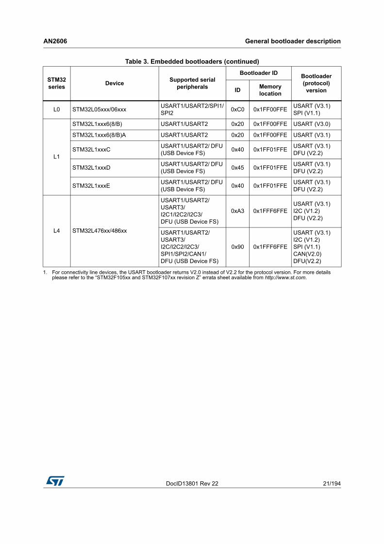
DocID13801 Rev 22 21/194
AN2606 General bootloader description
193
L0 STM32L05xxx/06xxxUSART1/USART2/SPI1/ SPI2
0xC0 0x1FF00FFEUSART (V3.1) SPI (V1.1)
L1
STM32L1xxx6(8/B) USART1/USART2 0x20 0x1FF00FFE USART (V3.0)
STM32L1xxx6(8/B)A USART1/USART2 0x20 0x1FF00FFE USART (V3.1)
STM32L1xxxCUSART1/USART2/ DFU (USB Device FS)
0x40 0x1FF01FFEUSART (V3.1) DFU (V2.2)
STM32L1xxxDUSART1/USART2/ DFU (USB Device FS)
0x45 0x1FF01FFEUSART (V3.1) DFU (V2.2)
STM32L1xxxEUSART1/USART2/ DFU (USB Device FS)
0x40 0x1FF01FFEUSART (V3.1) DFU (V2.2)
L4 STM32L476xx/486xx
USART1/USART2/ USART3/ I2C1/I2C2/I2C3/ DFU (USB Device FS)
0xA3 0x1FFF6FFEUSART (V3.1) I2C (V1.2) DFU (V2.2)
USART1/USART2/ USART3/ I2C/I2C2/I2C3/ SPI1/SPI2/CAN1/ DFU (USB Device FS)
0x90 0x1FFF6FFE
USART (V3.1) I2C (V1.2) SPI (V1.1) CAN(V2.0) DFU(V2.2)
1. For connectivity line devices, the USART bootloader returns V2.0 instead of V2.2 for the protocol version. For more details please refer to the “STM32F105xx and STM32F107xx revision Z” errata sheet available from http://www.st.com.
Table 3. Embedded bootloaders (continued)
STM32 series
DeviceSupported serial
peripherals
Bootloader ID Bootloader (protocol) versionID
Memory location

General bootloader description AN2606
22/194 DocID13801 Rev 22
3.3 Hardware connection requirements
To use the USART bootloader, the host has to be connected to the (RX) and (TX) pins of the desired USARTx interface via a serial cable.
Figure 1. USART Connection
1. A Pull-UP resistor should be added, if pull-up resistor are not connected in host side.2. An RS232 transceiver must be connected to adapt voltage level (3.3V - 12V) between STM32 device and
host.
Note: +V typically 3.3 V and R value typically 100KOhm.This value depend on the application and the used hardware.
To use the DFU, connect the microcontroller's USB interface to a USB host (i.e. PC).
Figure 2. USB Connection
1. This additional circuit permits to connect a Pull-Up resistor to (DP) pin using VBus when needed. Refer to product section (Table which describes STM32 Configuration in system memory boot mode) to know if an external pull-up resistor must be connected to (DP) pin.
Note: +V typically 3.3 V.This value depends on the application and the used hardware.

DocID13801 Rev 22 23/194
AN2606 General bootloader description
193
To use the I2C bootloader, connect the host (master) and the desired I2Cx interface (slave) together via the data (SDA) and clock (SCL) pins. A 1.8 KOhm pull-up resistor has to be connected to both (SDA) and (SCL) lines.
Figure 3. I2C Connection
Note: +V typically 3.3 V.This value depends on the application and the used hardware.
To use the SPI bootloader, connect the host (master) and the desired SPIx interface (slave) together via the (MOSI), (MISO) and (SCK) pins. The (NSS) pin must be connected to (GND). A pull-down resistor should be connected to the (SCK) line.
Figure 4. SPI Connection
Note: R value typically 10KOhm. This value depends on the application and the used hardware.
To use the CAN interface, the host has to be connected to the (RX) and (TX) pins of the desired CANx interface via CAN transceiver and a serial cable. A 120 Ohm resistor should be added as terminating resistor.

General bootloader description AN2606
24/194 DocID13801 Rev 22
Figure 5. CAN Connection
Note: When a bootloader firmware supports DFU, it is mandatory that no USB Host is connected to the USB peripheral during the selection phase of the other interfaces. After selection phase, the user can plug a USB cable without impacting the selected bootloader execution except commands which generate a system reset.
It is recommended to keep the RX pins of unused Bootloader interfaces (USART_RX, SPI_MOSI, CAN_RX and USB D+/D- lines if present) at a known (low or high) level at the startup of the Bootloader (detection phase). Leaving these pins floating during the detection phase might lead to activating unused interface.
3.4 Bootloader Memory Management
All write operations using bootloader commands must only be Word-aligned (the address should be a multiple of 4). The number of data to be written must also be a multiple of 4 (non-aligned half page write addresses are accepted).
Some Products embeds bootloader that has some specific features:
• Some products don’t support Mass erase operation. To perform a mass erase operation using bootloader, two options are available:
– Erase all sectors one by one using the Erase command
– Set protection level to Level 1. Then, set it to Level 0 (using the Read protect command and then the Read Unprotect command). This operation results in a mass erase of the internal Flash memory.
• Bootloader firmware of STM32 L1 and L0 series supports Data Memory in addition to standard memories (internal Flash, internal SRAM, option bytes and System memory). The start address and the size of this area depends on product, please refer to product reference manual for more information. Data memory can be read and written but cannot be erased using the Erase Command. When writing in a Data memory location, the bootloader firmware manages the erase operation of this location before any write. A write to Data memory must be Word-aligned (address to be written should be a multiple of 4) and the number of data must also be a multiple of 4. To erase a Data memory location, you can write zeros at this location.
• Bootloader firmware of STM32 F2, F4, F7 and L4 series supports OTP memory in addition to standard memories (internal Flash, internal SRAM, option bytes and System memory). The start address and the size of this area depends on product, please refer to product reference manual for more information. OTP memory can be read and

DocID13801 Rev 22 25/194
AN2606 General bootloader description
193
written but cannot be erased using Erase command. When writing in an OTP memory location, make sure that the relative protection bit is not reset.
• For STM32 F2, F4 and F7 series the internal flash write operation format depends on voltage Range. By default write operation are allowed by one byte format (Half-Word, Word and Double-Word operations are not allowed). to increase the speed of write operation, the user should apply the adequate voltage range that allows write operation by Half-Word, Word or Double-Word and update this configuration on the fly by the bootloader software through a virtual memory location. This memory location is not physical but can be read and written using usual bootloader read/write operations according to the protocol in use. This memory location contains 4 bytes which are described in table below. It can be accessed by 1, 2, 3 or 4 bytes. However, reserved bytes should remain at their default values (0xFF), otherwise the request will be NACKed.
Table 4. STM32 F2, F4 and F7 Voltage Range configuration using bootloader
The table below lists the valid memory area depending on the Bootloader commands.
Address Size Description
0xFFFF0000 1 byte
This byte controls the current value of the voltage range.
0x00: voltage range [1.8 V, 2.1 V]0x01: voltage range [2.1 V, 2.4 V]0x02: voltage range [2.4 V, 2.7 V]0x03: voltage range [2.7 V, 3.6 V]0x04: voltage range [2.7 V, 3.6 V] and double word write/erase operation is used. In this case it is mandatory to supply 9 V through the VPP pin (refer to the product reference manual for more details about the double-word write procedure).Other: all other values are not supported and will be NACKed.
0xFFFF0001 1 byteReserved.
0xFF: default value.Other: all other values are not supported and will be NACKed.
0xFFFF0002 1 byteReserved.
0xFF: default value.Other: all other values are not supported and will be NACKed.
0xFFFF0003 1 byteReserved.
0xFF: default value.Other: all other values are not supported and will be NACKed.
Table 5. Supported memory area by Write, Read, Erase and Go Commands
Memory Area Write command Read command Erase command Go command
Flash Supported Supported Supported Supported
RAM Supported Supported Not Supported Supported
System Memory Not Supported Supported Not Supported Not Supported
Data Memory Supported Supported Not Supported Not Supported
OTP Memory Supported Supported Not Supported Not Supported

STM32F03xx4/6 devices bootloader AN2606
26/194 DocID13801 Rev 22
4 STM32F03xx4/6 devices bootloader
4.1 Bootloader configuration
The STM32F03xx4/6 bootloader is activated by applying pattern2 (described in Table 2: Bootloader activation patterns). The following table shows the hardware resources used by this bootloader.
The system clock is derived from the embedded internal high-speed RC, no external quartz is required for the bootloader execution.
Note: After the STM32F03xx4/6 devices has booted in bootloader mode, serial wire debug (SWD) communication is no longer possible until the system is reset. This is because the SWD uses the PA14 pin (SWCLK) which is already used by the bootloader (USART1_TX).
Table 6. STM32F03xx4/6 configuration in system memory boot mode
Bootloader Feature/Peripheral State Comment
Common to all
bootloaders
RCC HSI EnabledThe system clock frequency is 24 MHz (using PLL clocked by HSI).
1 Flash Wait State.
RAM -2 Kbytes starting from address 0x20000000 are used by the bootloader firmware.
System memory -3 Kbytes starting from address 0x1FFFEC00 contain the bootloader firmware.
IWDG -
The independent watchdog (IWDG) prescaler is configured to its maximum value. It is periodically refreshed to prevent watchdog reset in case the hardware IWDG option was previously enabled by the user.
USART1
bootloader (on
PA10/PA9)
USART1 EnabledOnce initialized, the USART1 configuration is 8 bits, even parity and 1 Stop bit.
USART1_RX pin Input PA10 pin: USART1 in reception mode.
USART1_TX pin Output PA9 pin: USART1 in transmission mode.
USART1
bootloader (on
PA14/PA15)
USART1 EnabledOnce initialized, the USART1 configuration is 8 bits, even parity and 1 Stop bit.
USART1_RX pin Input PA15 pin: USART1 in reception mode.
USART1_TX pin Output PA14 pin: USART1 in transmission mode.
USART1
bootloadersSysTick timer Enabled
Used to automatically detect the serial baud rate from the host.
DocID13801 Rev 22 27/194
AN2606 STM32F03xx4/6 devices bootloader
193
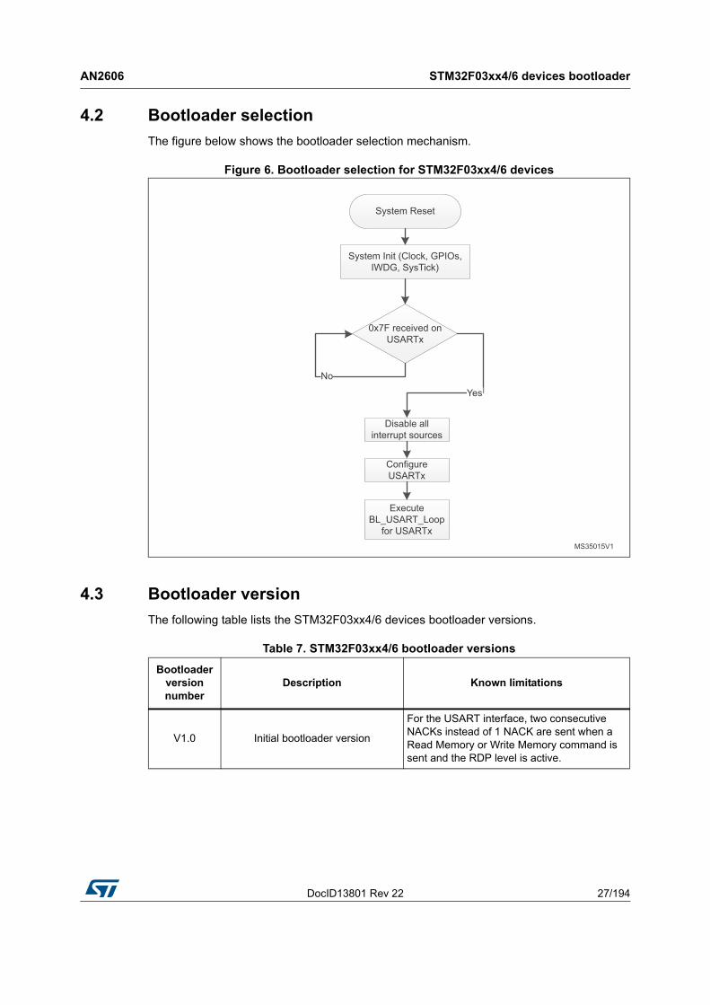
4.2 Bootloader selection
The figure below shows the bootloader selection mechanism.
Figure 6. Bootloader selection for STM32F03xx4/6 devices
4.3 Bootloader version
The following table lists the STM32F03xx4/6 devices bootloader versions.
Table 7. STM32F03xx4/6 bootloader versions
Bootloader version number
Description Known limitations
V1.0 Initial bootloader version
For the USART interface, two consecutive NACKs instead of 1 NACK are sent when a Read Memory or Write Memory command is sent and the RDP level is active.

STM32F030xC devices bootloader AN2606
28/194 DocID13801 Rev 22
5 STM32F030xC devices bootloader
5.1 Bootloader configuration
The STM32F030xC bootloader is activated by applying pattern6 (described in Table 2: Bootloader activation patterns). The following table shows the hardware resources used by this bootloader.
Note: After the STM32F030xC devices have booted in Bootloader mode using USART2, the serial wire debug (SWD) communication is no more possible until the system is reset, because SWD uses PA14 pin (SWCLK) which is already used by the Bootloader (USART2_RX).
The system clock is derived from the embedded internal high-speed RC, no external quartz is required for the bootloader execution.
Table 8.STM32F030xC configuration in system memory boot mode
Bootloader Feature/Peripheral State Comment
Common to all bootloaders
RCC HSI enabledThe system clock configured to 48 MHz with HSI 8 MHz as clock source.
RAM -6 Kbytes starting from address 0x20000000 are used by the bootloader firmware
System memory -8 Kbytes starting from address 0x1FFFD800, contain the bootloader firmware.
USART1 bootloader
USART1 EnabledOnce initialized the USART1 configuration is: 8-bits, even parity and 1 Stop bit
USART1_RX pin Input PA10 pin: USART1 in reception mode
USART1_TX pin Output PA9 pin: USART1 in transmission mode
USART2 bootloader
USART2 EnabledOnce initialized the USART2 configuration is: 8-bits, even parity and 1 Stop bit
USART2_RX pin Input PA15 pin: USART2 in reception mode
USART2_TX pin Output PA14 pin: USART2 in transmission mode
USART1 and USART2 bootloaders
SysTick timer EnabledUsed to automatically detect the serial baud rate from the host for USARTx bootloaders.
I2C1 bootloader
I2C1 Enabled
The I2C1 configuration is: I2C speed: up to 400 KHz, 7-bit address, slave mode, analog filter ON. Slave 7-bit address: 0b1000001x (where x = 0 for write and x = 1 for read)
I2C1_SCL pin Input/OutputPB6 pin: clock line is used in open-drain mode.
I2C1_SDA pin Input/OutputPB7 pin: data line is used in open-drain mode.

DocID13801 Rev 22 29/194
AN2606 STM32F030xC devices bootloader
193
5.2 Bootloader selection
The figure below shows the bootloader selection mechanism.
Figure 7.Bootloader selection for STM32F030xC
5.3 Bootloader version
The following table lists the STM32F030xC devices bootloader versions.
Table 9.STM32F030xC bootloader versions
Bootloader version number
Description Known limitations
V5.2 Initial bootloader version None

STM32F05xxx and STM32F030x8 devices bootloader AN2606
30/194 DocID13801 Rev 22
6 STM32F05xxx and STM32F030x8 devices bootloader
6.1 Bootloader configuration
The STM32F05xxx and STM32F030x8 devices bootloader is activated by applying pattern2 (described in Table 2: Bootloader activation patterns). The following table shows the hardware resources used by this bootloader.
The system clock is derived from the embedded internal high-speed RC, no external quartz is required for the bootloader execution.
Note: After the STM32F05xxx and STM32F030x8 devices have booted in bootloader mode, the serial wire debug (SWD) communication is no more possible until the system is reset, because SWD uses PA14 pin (SWCLK) which is already used by the bootloader (USART2_TX).
Table 10. STM32F05xxx and STM32F030x8 devices configuration in system memory boot mode
Bootloader Feature/Peripheral State Comment
Common to all
bootloaders
RCC HSI EnabledThe system clock frequency is 24 MHz (using PLL clocked by HSI).
1 Flash Wait State.
RAM -2 Kbytes starting from address 0x20000000 are used by the bootloader firmware.
System memory -3 Kbytes starting from address 0x1FFFEC00, contain the bootloader firmware.
IWDG -
The independent watchdog (IWDG) prescaler is configured to its maximum value. It is periodically refreshed to prevent watchdog reset in case the hardware IWDG option was previously enabled by the user.
USART1
bootloader
USART1 EnabledOnce initialized, the USART1 configuration is 8 bits, even parity and 1 Stop bit.
USART1_RX pin Input PA10 pin: USART1 in reception mode.
USART1_TX pin Output PA9 pin: USART1 in transmission mode.
USART2
bootloader
USART2 EnabledOnce initialized, the USART2 configuration is 8 bits, even parity and 1 Stop bit.
USART2_RX pin Input PA15 pin: USART2 in reception mode.
USART2_TX pin Output PA14 pin: USART2 in transmission mode.
USART1 and
USART2
bootloaders
SysTick timer EnabledUsed to automatically detect the serial baud rate from the host.
DocID13801 Rev 22 31/194
AN2606 STM32F05xxx and STM32F030x8 devices bootloader
193
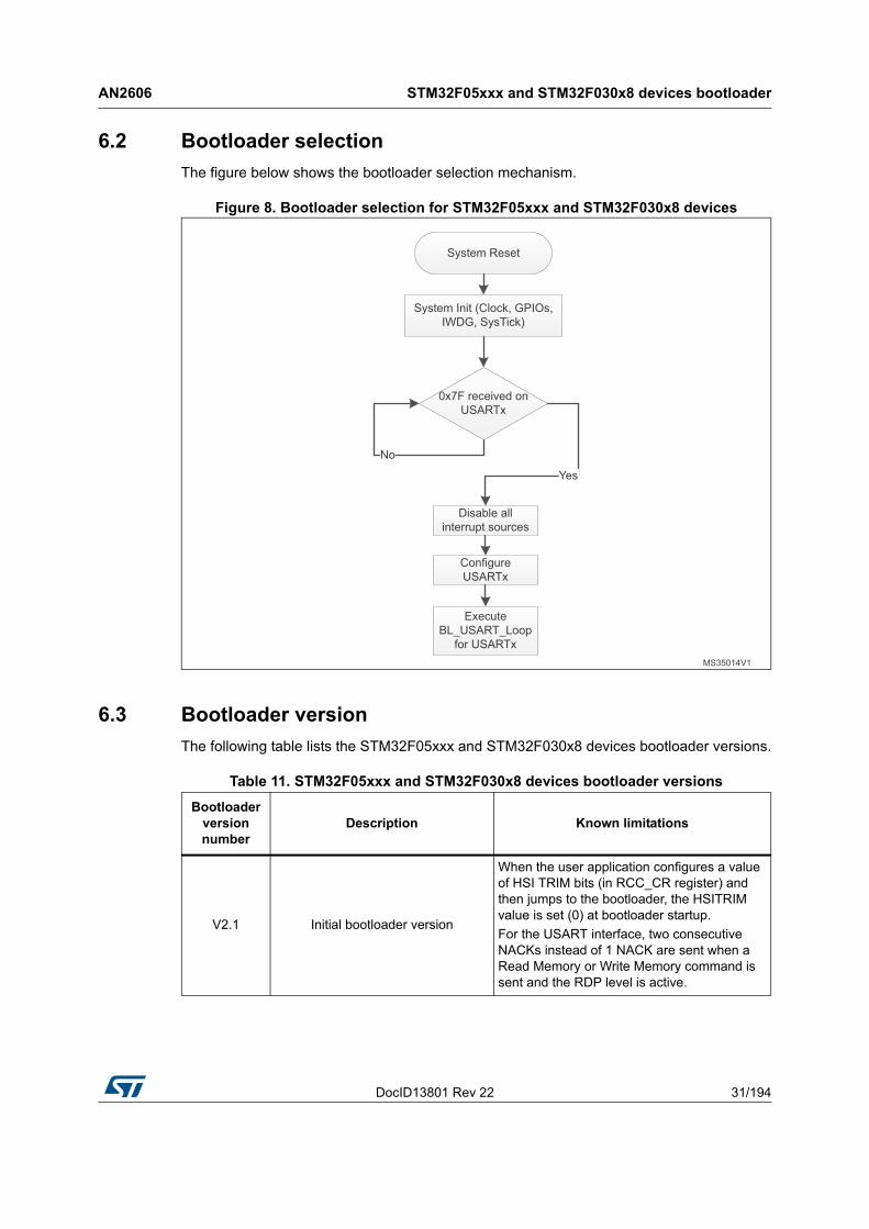
6.2 Bootloader selection
The figure below shows the bootloader selection mechanism.
Figure 8. Bootloader selection for STM32F05xxx and STM32F030x8 devices
6.3 Bootloader version
The following table lists the STM32F05xxx and STM32F030x8 devices bootloader versions.
Table 11. STM32F05xxx and STM32F030x8 devices bootloader versions
Bootloader version number
Description Known limitations
V2.1 Initial bootloader version
When the user application configures a value of HSI TRIM bits (in RCC_CR register) and then jumps to the bootloader, the HSITRIM value is set (0) at bootloader startup.
For the USART interface, two consecutive NACKs instead of 1 NACK are sent when a Read Memory or Write Memory command is sent and the RDP level is active.

STM32F04xxx devices bootloader AN2606
32/194 DocID13801 Rev 22
7 STM32F04xxx devices bootloader
7.1 Bootloader configuration
The STM32F04xxx bootloader is activated by applying pattern6 (described in Table 2: Bootloader activation patterns). The following table shows the hardware resources used by this bootloader.
Table 12. STM32F04xxx configuration in system memory boot mode
Bootloader Feature/Peripheral State Comment
Common to all
bootloaders
RCC
HSI enabledThe system clock frequency is 48 MHz with HSI 48 MHz as clock source.
-The Clock Recovery System (CRS) is enabled for the DFU bootloaders to allow USB to be clocked by HSI 48 MHz.
RAM -6 Kbytes starting from address 0x20000000 are used by the bootloader firmware
System memory -13 Kbytes starting from address 0x1FFFC400, contain the bootloader firmware
IWDG -
The independent watchdog (IWDG) prescaler is configured to its maximum value. It is periodically refreshed to prevent watchdog reset (in case the hardware IWDG option was previously enabled by the user).
USART1
bootloader
USART1 EnabledOnce initialized the USART1 configuration is: 8-bits, even parity and 1 Stop bit
USART1_RX pin Input PA10 pin: USART1 in reception mode
USART1_TX pin Output PA9 pin: USART1 in transmission mode
USART2
bootloader
USART2 EnabledOnce initialized the USART2 configuration is: 8-bits, even parity and 1 Stop bit
USART2_RX pin Input PA15 pin: USART2 in reception mode
USART2_TX pin Output PA14 pin: USART2 in transmission mode
USART1 and
USART2
bootloaders
SysTick timer EnabledUsed to automatically detect the serial baud rate from the host for USARTx bootloaders.

DocID13801 Rev 22 33/194
AN2606 STM32F04xxx devices bootloader
193
Note: After the STM32F04xxx devices have booted in Bootloader mode using USART2, the serial wire debug (SWD) communication is no more possible until the system is reset, because SWD uses PA14 pin (SWCLK) which is already used by the Bootloader (USART2_RX).
The system clock is derived from the embedded internal high-speed RC, no external quartz is required for the bootloader execution.
I2C1 bootloader
I2C1 Enabled
The I2C1configuration is: I2C speed: up to 400 KHz, 7-bit address, slave mode, analog filter ON. Slave 7-bit address: 0b0111110x (where x = 0 for write and x = 1 for read).
I2C1_SCL pin Input/OutputPB6 pin: clock line is used in open-drain mode.
I2C1_SDA pin Input/OutputPB7 pin: data line is used in open-drain mode.
DFU bootloader
USB Enabled USB used in FS mode
USB_DM pin
Input/Output
PA11: USB DM line.
USB_DP pinPA12: USB DP line
No external pull-up resistor is required.
Table 12. STM32F04xxx configuration in system memory boot mode (continued)
Bootloader Feature/Peripheral State Comment
STM32F04xxx devices bootloader AN2606
34/194 DocID13801 Rev 22
7.2 Bootloader selection
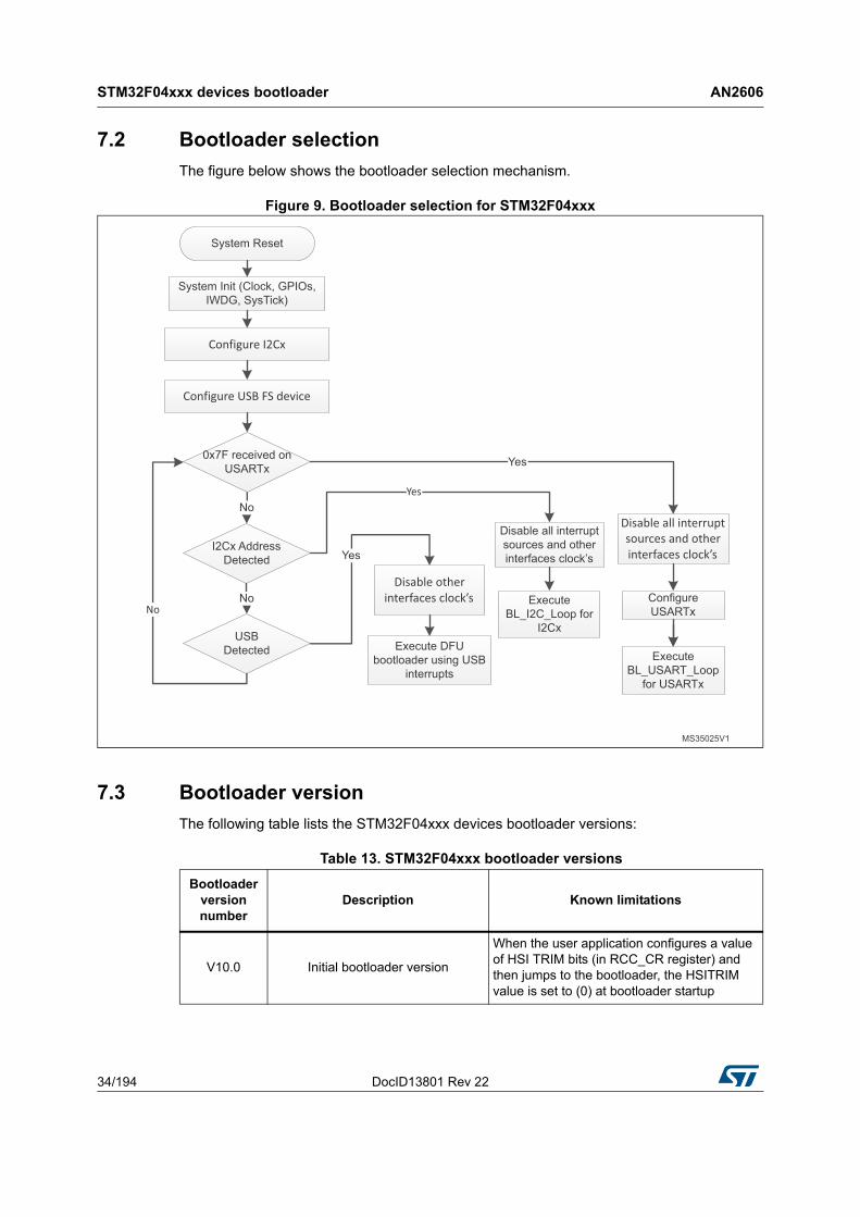
The figure below shows the bootloader selection mechanism.
Figure 9. Bootloader selection for STM32F04xxx
7.3 Bootloader version
The following table lists the STM32F04xxx devices bootloader versions:
Table 13. STM32F04xxx bootloader versions
Bootloader version number
Description Known limitations
V10.0 Initial bootloader version
When the user application configures a value of HSI TRIM bits (in RCC_CR register) and then jumps to the bootloader, the HSITRIM value is set to (0) at bootloader startup
DocID13801 Rev 22 35/194
AN2606 STM32F070x6 devices bootloader
193
8 STM32F070x6 devices bootloader
8.1 Bootloader configuration
The STM32F070x6 bootloader is activated by applying pattern6 (described in Table 2: Bootloader activation patterns). The following table shows the hardware resources used by this bootloader.
Table 14. STM32F070x6 configuration in system memory boot mode
BootloaderFeature/Periphe
ralState Comment
Common to all
bootloaders
RCC
HSI enabledAt startup, the system clock frequency is configured to 48 MHz using the HSI. If an external clock (HSE) is not present, the system is kept clocked from the HSI.
HSE enabled
The external clock can be used for all bootloader interfaces and should have one of the following values 24,18,12,8,6,4 MHz. The PLL is used to generate 48 MHz for USB and system clock.
-The Clock Security System (CSS) interrupt is enabled for HSE. Any failure (or removal) of the external clock generates system reset.
RAM -6 Kbytes starting from address 0x20000000 are used by the bootloader firmware
System memory -13 Kbytes starting from address 0x1FFFC400, contain the bootloader firmware.
USART1
bootloader
USART1 EnabledOnce initialized the USART1 configuration is: 8-bits, even parity and 1 Stop bit
USART1_RX pin Input PA10 pin: USART1 in reception mode
USART1_TX pin Output PA9 pin: USART1 in transmission mode
USART2
bootloader
USART2 EnabledOnce initialized the USART2 configuration is: 8-bits, even parity and 1 Stop bit
USART2_RX pin Input PA15 pin: USART2 in reception mode
USART2_TX pin Output PA14 pin: USART2 in transmission mode
USART1 and
USART2
bootloaders
SysTick timer EnabledUsed to automatically detect the serial baud rate from the host for USARTx bootloaders.
I2C1 bootloader
I2C1 Enabled
The I2C1 configuration is:
I2C speed: up to 400 KHz, 7-bit address, slave mode, analog filter ON.
Slave 7-bit address: 0b0111110x where x = 0 for write and x = 1 for read)
I2C1_SCL pin Input/Output PB6 pin: clock line is used in open-drain mode.
I2C1_SDA pin Input/Output PB7 pin: data line is used in open-drain mode.
STM32F070x6 devices bootloader AN2606
36/194 DocID13801 Rev 22
Note: If HSI deviation exceeds 1% , the bootloader might not function correctly.
Note: After the STM32F070x6 devices have booted in Bootloader mode using USART2, the serial wire debug (SWD) communication is no more possible until the system is reset, because SWD uses PA14 pin (SWCLK) which is already used by the Bootloader (USART2_RX).
The bootloader has two cases of operation depending on the presence of the external clock (HSE) at bootloader startup:
• If HSE is present and has a value of 24, 18, 16, 12, 8, 6, 4 MHz, the system clock is configured to 48 MHz with HSE as clock source. The DFU interface, USART1, USART2 and I2C1 are functional and can be used to communicate with the bootloader device.
• If HSE is not present, the HSI is kept as default clock source and only USART1, USART2 and I2C1 are functional.
The external clock (HSE) must be kept if it’s connected at bootloader startup because it will be used as system clock source.
DFU bootloader
USB EnabledUSB FS configured in Forced Device mode. USB FS interrupt vector is enabled and used for USB DFU communications.
USB_DM pin
Input/Output
PA11 pin: USB FS DM line
USB_DP pinPA12 pin: USB FS DP line.
No external Pull-up resistor is required.
Table 14. STM32F070x6 configuration in system memory boot mode (continued)
BootloaderFeature/Periphe
ralState Comment

DocID13801 Rev 22 37/194
AN2606 STM32F070x6 devices bootloader
193
8.2 Bootloader selection
The figure below shows the bootloader selection mechanism.
Figure 10.Bootloader selection for STM32F070x6

STM32F070x6 devices bootloader AN2606
38/194 DocID13801 Rev 22
8.3 Bootloader version
The following table lists the STM32F070x6 devices bootloader versions.
Table 15.STM32F070x6 bootloader versions
Bootloader version number
Description Known limitations
V10.2 Initial bootloader version
When the user application configures a value of HSI TRIM bits (in RCC_CR register) and then jumps to the bootloader, the HSITRIM value is set to (0) at bootloader startup.
V10.3Clock configuration fixed
to HSI 8 MHz
When the user application configures a value of HSI TRIM bits (in RCC_CR register) and then jumps to the bootloader, the HSITRIM value is set to (0) at bootloader startup.

DocID13801 Rev 22 39/194
AN2606 STM32F070xB devices bootloader
193
9 STM32F070xB devices bootloader
9.1 Bootloader configuration
The STM32F070xB bootloader is activated by applying pattern2 (described in Table 2: Bootloader activation patterns). The following table shows the hardware resources used by this bootloader.
Table 16. STM32F070xB configuration in system memory boot mode
Bootloader Feature/Peripheral State Comment
Common to all
bootloaders
RCC
HSI enabled
At startup, the system clock frequency is configured to 48 MHz using the HSI. If an external clock (HSE) is not present, the system is kept clocked from the HSI.
HSE enabled
The external clock can be used for all bootloader interfaces and should have one of the following values 24,18,12,8,6,4 MHz. The PLL is used to generate 48 MHz for USB and system clock.
-
The Clock Security System (CSS) interrupt is enabled for HSE. Any failure (or removal) of the external clock generates system reset.
RAM -6 Kbytes starting from address 0x20000000 are used by the bootloader firmware
System memory -12 Kbytes starting from address 0x1FFFC800, contain the bootloader firmware.
USART1
bootloader
USART1 EnabledOnce initialized the USART1 configuration is: 8-bits, even parity and 1 Stop bit
USART1_RX pin Input PA10 pin: USART1 in reception mode
USART1_TX pin Output PA9 pin: USART1 in transmission mode
USART2
bootloader
USART2 EnabledOnce initialized the USART2 configuration is: 8-bits, even parity and 1 Stop bit
USART2_RX pin Input PA15 pin: USART2 in reception mode
USART2_TX pin Output PA14 pin: USART2 in transmission mode
USART1 and
USART2
bootloaders
SysTick timer EnabledUsed to automatically detect the serial baud rate from the host for USARTx bootloaders.
I2C1 bootloader
I2C1 Enabled
The I2C1 configuration is:
I2C speed: up to 400 KHz, 7-bit address, slave mode, analog filter ON.
Slave 7-bit address: 0b0111011x
(where x = 0 for write and x = 1 for read)
I2C1_SCL pin Input/OutputPB6 pin: clock line is used in open-drain mode.
I2C1_SDA pin Input/OutputPB7 pin: data line is used in open-drain mode.

STM32F070xB devices bootloader AN2606
40/194 DocID13801 Rev 22
Note: If HSI deviation exceeds 1% , the bootloader might not function correctly.
Note: After the STM32F070xB devices have booted in Bootloader mode using USART2, the serial wire debug (SWD) communication is no more possible until the system is reset, because SWD uses PA14 pin (SWCLK) which is already used by the Bootloader (USART2_RX).
The bootloader has two cases of operation depending on the presence of the external clock (HSE) at bootloader startup:
• If HSE is present and has a value of 24, 18, 16, 12, 8, 6, 4 MHz, the system clock is configured to 48 MHz with HSE as clock source. The DFU interface, USART1, USART2 and I2C1 are functional and can be used to communicate with the bootloader device.
• If HSE is not present, the HSI is kept as default clock source and only USART1, USART2 and I2C1 are functional.
The external clock (HSE) must be kept if it’s connected at bootloader startup because it will be used as system clock source.
DFU bootloader
USB EnabledUSB FS configured in Forced Device mode. USB FS interrupt vector is enabled and used for USB DFU communications.
USB_DM pin
Input/Output
PA11 pin: USB FS DM line
USB_DP pinPA12 pin: USB FS DP line.
No external Pull-up resistor is required.
Table 16. STM32F070xB configuration in system memory boot mode (continued)
Bootloader Feature/Peripheral State Comment

DocID13801 Rev 22 41/194
AN2606 STM32F070xB devices bootloader
193
9.2 Bootloader selection
The figure below shows the bootloader selection mechanism.
Figure 11.Bootloader selection for STM32F070xB

STM32F070xB devices bootloader AN2606
42/194 DocID13801 Rev 22
9.3 Bootloader version
The following table lists the STM32F070xB devices bootloader versions.
Table 17.STM32F070xB bootloader versions
Bootloader version number
Description Known limitations
V10.2 Initial bootloader version
When the user application configures a value of HSI TRIM bits (in RCC_CR register) and then jumps to the bootloader, the HSITRIM value is set to (0) at bootloader startup.
V10.3Clock configuration fixed
to HSI 8 MHz
When the user application configures a value of HSI TRIM bits (in RCC_CR register) and then jumps to the bootloader, the HSITRIM value is set to (0) at bootloader startup.
DocID13801 Rev 22 43/194
AN2606 STM32F071xx/72xx devices bootloader
193
10 STM32F071xx/72xx devices bootloader
10.1 Bootloader configuration
The STM32F071xx/72xx bootloader is activated by applying pattern2 (described in Table 2: Bootloader activation patterns). The following table shows the hardware resources used by this bootloader.
Table 18. STM32F071xx/72xx configuration in system memory boot mode
Bootloader Feature/Peripheral State Comment
Common to all
bootloaders
RCC
HSI enabledThe system clock frequency is 48 MHz with HSI 48 MHz as clock source.
-The Clock Recovery System (CRS) is enabled for the DFU bootloaders to allow USB to be clocked by HSI 48 MHz.
RAM -6 Kbytes starting from address 0x20000000 are used by the bootloader firmware
System memory -12 Kbytes starting from address 0x1FFFC800, contain the bootloader firmware
IWDG -
The independent watchdog (IWDG) prescaler is configured to its maximum value. It is periodically refreshed to prevent watchdog reset (in case the hardware IWDG option was previously enabled by the user).
USART1
bootloader
USART1 EnabledOnce initialized the USART1 configuration is: 8-bits, even parity and 1 Stop bit
USART1_RX pin Input PA10 pin: USART1 in reception mode
USART1_TX pin Output PA9 pin: USART1 in transmission mode
USART2
bootloader
USART2 EnabledOnce initialized the USART2 configuration is: 8-bits, even parity and 1 Stop bit
USART2_RX pin Input PA15 pin: USART2 in reception mode
USART2_TX pin Output PA14 pin: USART2 in transmission mode
USART1 and
USART2
bootloaders
SysTick timer EnabledUsed to automatically detect the serial baud rate from the host for USARTx bootloaders.

STM32F071xx/72xx devices bootloader AN2606
44/194 DocID13801 Rev 22
Note: After the STM32F071xx/72xx devices have booted in Bootloader mode using USART2, the serial wire debug (SWD) communication is no more possible until the system is reset, because SWD uses PA14 pin (SWCLK) which is already used by the Bootloader (USART2_RX).
The system clock is derived from the embedded internal high-speed RC, no external quartz is required for the bootloader execution.
I2C1 bootloader
I2C1 Enabled
The I2C1 configuration is: I2C speed: up to 400 KHz, 7-bit address, slave mode, analog filter ON. Slave 7-bit address: 0b0111011x (where x = 0 for write and x = 1 for read)
I2C1_SCL pin Input/OutputPB6 pin: clock line is used in open-drain mode.
I2C1_SDA pin Input/OutputPB7 pin: data line is used in open-drain mode.
DFU bootloader
USB Enabled USB used in FS mode
USB_DM pin
Input/Output
PA11: USB DM line.
USB_DP pinPA12: USB DP line
No external pull-up resistor is required.
Table 18. STM32F071xx/72xx configuration in system memory boot mode (continued)
Bootloader Feature/Peripheral State Comment

DocID13801 Rev 22 45/194
AN2606 STM32F071xx/72xx devices bootloader
193
10.2 Bootloader selection
The figure below shows the bootloader selection mechanism.
Figure 12. Bootloader selection for STM32F071xx/72xx
10.3 Bootloader version
The following table lists the STM32F071xx/72xx devices bootloader versions:
Table 19. STM32F071xx/72xx bootloader versions
Bootloader version number
Description Known limitations
V10.1 Initial bootloader version
When the user application configures a value of HSI TRIM bits (in RCC_CR register) and then jumps to the bootloader, the HSITRIM value is set to (0) at bootloader startup

STM32F09xxx devices bootloader AN2606
46/194 DocID13801 Rev 22
11 STM32F09xxx devices bootloader
11.1 Bootloader configuration
The STM32F09xxx bootloader is activated by applying pattern6 (described in Table 2: Bootloader activation patterns). The following table shows the hardware resources used by this bootloader.
Note: After the STM32F09xxx devices have booted in Bootloader mode using USART2, the serial wire debug (SWD) communication is no more possible until the system is reset, because SWD uses PA14 pin (SWCLK) which is already used by the Bootloader (USART2_RX).
The system clock is derived from the embedded internal high-speed RC, no external quartz is required for the bootloader execution.
Table 20.STM32F09xxx configuration in system memory boot mode
Bootloader Feature/Peripheral State Comment
Common to all bootloaders
RCC HSI enabledThe system clock configured to 48 MHz with HSI 48 MHz as clock source.
RAM -6 Kbytes starting from address 0x20000000 are used by the bootloader firmware
System memory -8 Kbytes starting from address 0x1FFFD800, contain the bootloader firmware.
USART1 bootloader
USART1 EnabledOnce initialized the USART1 configuration is: 8-bits, even parity and 1 Stop bit
USART1_RX pin Input PA10 pin: USART1 in reception mode
USART1_TX pin Output PA9 pin: USART1 in transmission mode
USART2 bootloader
USART2 EnabledOnce initialized the USART2 configuration is: 8-bits, even parity and 1 Stop bit
USART2_RX pin Input PA15 pin: USART2 in reception mode
USART2_TX pin Output PA14 pin: USART2 in transmission mode
USART1 and USART2 bootloaders
SysTick timer EnabledUsed to automatically detect the serial baud rate from the host for USARTx bootloaders.
I2C1 bootloader
I2C1 Enabled
The I2C1 configuration is: I2C speed: up to 400 KHz, 7-bit address, slave mode, analog filter ON. Slave 7-bit address: 0b1000001x (where x = 0 for write and x = 1 for read)
I2C1_SCL pin Input/OutputPB6 pin: clock line is used in open-drain mode.
I2C1_SDA pin Input/OutputPB7 pin: data line is used in open-drain mode.

DocID13801 Rev 22 47/194
AN2606 STM32F09xxx devices bootloader
193
11.2 Bootloader selection
The figure below shows the bootloader selection mechanism.
Figure 13. Bootloader selection for STM32F09xxx
11.3 Bootloader version
The following table lists the STM32F09xxx devices bootloader versions.
Table 21.STM32F09xxx bootloader versions
Bootloader version number
Description Known limitations
V5.0 Initial bootloader version
When the user application configures a value of HSI TRIM bits (in RCC_CR register) and then jumps to the bootloader, the HSITRIM value is set to (0) at bootloader startup.

STM32F10xxx devices bootloader AN2606
48/194 DocID13801 Rev 22
12 STM32F10xxx devices bootloader
12.1 Bootloader configuration
The STM32F10xxx bootloader is activated by applying pattern1 (described in Table 2: Bootloader activation patterns). The following table shows the hardware resources used by this bootloader.
The system clock is derived from the embedded internal high-speed RC, no external quartz is required for the bootloader execution.
Table 22. STM32F10xxx configuration in system memory boot mode
Bootloader Feature/Peripheral State Comment
USART1
bootloader
RCC HSI enabledThe system clock frequency is 24 MHz using the PLL.
RAM -512 bytes starting from address 0x20000000 are used by the bootloader firmware.
System memory -2 Kbytes starting from address 0x1FFFF000 contain the bootloader firmware.
IWDG -
The independent watchdog (IWDG) prescaler is configured to its maximum value and is periodically refreshed to prevent watchdog reset (in case the hardware IWDG option was previously enabled by the user).
USART1 EnabledOnce initialized, the USART1 configuration is: 8 bits, even parity and 1 Stop bit.
USART1_RX pin Input PA10 pin: USART1 in reception mode
USART1_TX pin Output push-pull PA9 pin: USART1 in transmission mode
SysTick timer EnabledUsed to automatically detect the serial baud rate from the host.
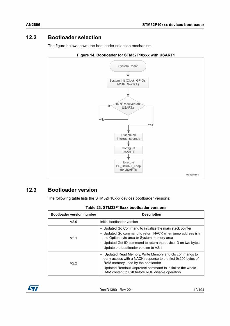
DocID13801 Rev 22 49/194
AN2606 STM32F10xxx devices bootloader
193
12.2 Bootloader selection
The figure below shows the bootloader selection mechanism.
Figure 14. Bootloader for STM32F10xxx with USART1
12.3 Bootloader version
The following table lists the STM32F10xxx devices bootloader versions:
Table 23. STM32F10xxx bootloader versions
Bootloader version number Description
V2.0 Initial bootloader version
V2.1
– Updated Go Command to initialize the main stack pointer
– Updated Go command to return NACK when jump address is in the Option byte area or System memory area
– Updated Get ID command to return the device ID on two bytes
– Update the bootloader version to V2.1
V2.2
– Updated Read Memory, Write Memory and Go commands to deny access with a NACK response to the first 0x200 bytes of RAM memory used by the bootloader
– Updated Readout Unprotect command to initialize the whole RAM content to 0x0 before ROP disable operation
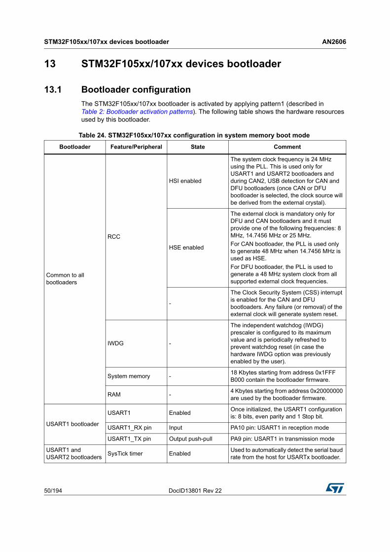
STM32F105xx/107xx devices bootloader AN2606
50/194 DocID13801 Rev 22
13 STM32F105xx/107xx devices bootloader
13.1 Bootloader configuration
The STM32F105xx/107xx bootloader is activated by applying pattern1 (described in Table 2: Bootloader activation patterns). The following table shows the hardware resources used by this bootloader.
Table 24. STM32F105xx/107xx configuration in system memory boot mode
Bootloader Feature/Peripheral State Comment
Common to all bootloaders
RCC
HSI enabled
The system clock frequency is 24 MHz using the PLL. This is used only for USART1 and USART2 bootloaders and during CAN2, USB detection for CAN and DFU bootloaders (once CAN or DFU bootloader is selected, the clock source will be derived from the external crystal).
HSE enabled
The external clock is mandatory only for DFU and CAN bootloaders and it must provide one of the following frequencies: 8 MHz, 14.7456 MHz or 25 MHz.
For CAN bootloader, the PLL is used only to generate 48 MHz when 14.7456 MHz is used as HSE.
For DFU bootloader, the PLL is used to generate a 48 MHz system clock from all supported external clock frequencies.
-
The Clock Security System (CSS) interrupt is enabled for the CAN and DFU bootloaders. Any failure (or removal) of the external clock will generate system reset.
IWDG -
The independent watchdog (IWDG) prescaler is configured to its maximum value and is periodically refreshed to prevent watchdog reset (in case the hardware IWDG option was previously enabled by the user).
System memory -18 Kbytes starting from address 0x1FFF B000 contain the bootloader firmware.
RAM -4 Kbytes starting from address 0x20000000 are used by the bootloader firmware.
USART1 bootloader
USART1 EnabledOnce initialized, the USART1 configuration is: 8 bits, even parity and 1 Stop bit.
USART1_RX pin Input PA10 pin: USART1 in reception mode
USART1_TX pin Output push-pull PA9 pin: USART1 in transmission mode
USART1 and USART2 bootloaders
SysTick timer EnabledUsed to automatically detect the serial baud rate from the host for USARTx bootloader.
DocID13801 Rev 22 51/194
AN2606 STM32F105xx/107xx devices bootloader
193
The system clock is derived from the embedded internal high-speed RC for USARTx bootloader. This internal clock is used also for DFU and CAN bootloaders but only for the selection phase. An external clock (8 MHz, 14.7456 MHz or 25 MHz.) is required for DFU and CAN bootloader execution after the selection phase.
USART2 bootloader
USART2 EnabledOnce initialized, the USART2 configuration is: 8 bits, even parity and 1 Stop bit. The USART2 uses its remapped pins.
USART2_RX pin Input PD6 pin: USART2 receive (remapped pin)
USART2_TX pin Output push-pull PD5 pin: USART2 transmit (remapped pin)
CAN2 bootloader
CAN2 Enabled
Once initialized, the CAN2 configuration is: Baudrate 125 kbps, 11-bit identifier.
Note: CAN1 is clocked during the CAN bootloader execution because CAN1 manages the communication between CAN2 and SRAM.
CAN2_RX pin Input PB5 pin: CAN2 receives (remapped pin).
CAN2_TX pin Output push-pull PB6 pin: CAN2 transmits (remapped pin).
DFU bootloader
USB EnabledUSB OTG FS configured in Forced Device mode
USB_VBUS pin Input PA9: Power supply voltage line
USB_DM pin
Input/Output
PA11 pin: USB_DM line
USB_DP pinPA12 pin: USB_DP line. No external Pull-up resistor is required
Table 24. STM32F105xx/107xx configuration in system memory boot mode (continued)
Bootloader Feature/Peripheral State Comment

STM32F105xx/107xx devices bootloader AN2606
52/194 DocID13801 Rev 22
13.2 Bootloader selection
The figure below shows the bootloader selection mechanism.
Figure 15. Bootloader selection for STM32F105xx/107xx devices

DocID13801 Rev 22 53/194
AN2606 STM32F105xx/107xx devices bootloader
193
13.3 Bootloader version
The following table lists the STM32F105xx/107xx devices bootloader versions:
Table 25. STM32F105xx/107xx bootloader versions
13.3.1 How to identify STM32F105xx/107xx bootloader versions
Bootloader V1.0 is implemented on devices which date code is below 937 (refer to STM32F105xx and STM32F107xx datasheet for where to find the date code on the device marking). Bootloader V2.0 and V2.1 are implemented on devices with a date code higher or equal to 937.
There are two ways to distinguish between bootloader versions:
• When using the USART bootloader, the Get-Version command defined in AN2606 and AN3155 has been corrected in V2.1 version. It returns 0x22 instead of 0x20 as in bootloader V2.0.
Bootloader version number
Description
V1.0 Initial bootloader version
V2.0
– Bootloader detection mechanism updated to fix the issue when GPIOs of unused peripherals in this bootloader are connected to low level or left floating during the detection phase. For more details please refer to Section 5.3.2.
– Vector table set to 0x1FFF B000 instead of 0x0000 0000
– Go command updated (for all bootloaders): USART1, USART2, CAN2, GPIOA, GPIOB, GPIOD and SysTick peripheral registers are set to their default reset values
– DFU bootloader: USB pending interrupt cleared before executing the Leave DFU command
– DFU subprotocol version changed from V1.0 to V1.2
– Bootloader version updated to V2.0
V2.1
– Fixed PA9 excessive consumption described in Section 5.3.4.
– Get-Version command (defined in AN3155) corrected. It returns 0x22 instead of 0x20 in bootloader V2.0. Refer to Section 5.3.3 for more details.
– Bootloader version updated to V2.1
V2.2
– Fixed DFU option bytes descriptor (set to ‘e’ instead of ‘g’ because it is read/write and not erasable).
– Fixed DFU polling timings for Flash Read/Write/Erase operations.
– Robustness enhancements for DFU bootloader interface.
– Updated bootloader version to V2.2.
STM32F105xx/107xx devices bootloader AN2606
54/194 DocID13801 Rev 22
• The values of the vector table at the beginning of the bootloader code are different. The user software (or via JTAG/SWD) reads 0x1FFFE945 at address 0x1FFFB004 for bootloader V2.0 0x1FFFE9A1 for bootloader V2.1, and 0x1FFFE9C1 for bootloader V2.2.
• The DFU version is the following:
– V2.1 in bootloader V2.1
– V2.2 in bootloader V2.2.
It can be read through the bcdDevice field of the DFU Device Descriptor.
13.3.2 Bootloader unavailability on STM32F105xx/STM32F107xx devices with a date code below 937
Description
The bootloader cannot be used if the USART1_RX (PA10), USART2_RX (PD6, remapped), CAN2_Rx (PB5, remapped), OTG_FS_DM (PA11), and/or OTG_FS_DP (PA12) pin(s) are held low or left floating during the bootloader activation phase.
The bootloader cannot be connected through CAN2 (remapped), DFU (OTG FS in Device mode), USART1 or USART2 (remapped).
On 64-pin packages, the USART2_RX signal remapped PD6 pin is not available and it is internally grounded. In this case, the bootloader cannot be used at all.
Workaround
• For 64-pin packages
None. The bootloader cannot be used.
• For 100-pin packages
Depending on the used peripheral, the pins for the unused peripherals have to be kept at a high level during the bootloader activation phase as described below:
– If USART1 is used to connect to the bootloader, PD6 and PB5 have to be kept at a high level.
– If USART2 is used to connect to the bootloader, PA10, PB5, PA11 and PA12 have to be kept at a high level.
– If CAN2 is used to connect to the bootloader, PA10, PD6, PA11 and PA12 have to be kept at a high level.
– If DFU is used to connect to the bootloader, PA10, PB5 and PD6 have to be kept at a high level.
Note: This limitation applies only to STM32F105xx and STM32F107xx devices with a date code below 937. STM32F105xx and STM32F107xx devices with a date code higher or equal to 937 are not impacted. See STM32F105xx and STM32F107xx datasheets for where to find the date code on the device marking.

DocID13801 Rev 22 55/194
AN2606 STM32F105xx/107xx devices bootloader
193
13.3.3 USART bootloader Get-Version command returns 0x20 instead of 0x22
Description
In USART mode, the Get-Version command (defined in AN3155) returns 0x20 instead of 0x20.
This limitation is present on bootloader versions V1.0 and V2.0, while it is fixed in bootloader version 2.1.
Workaround
None.
13.3.4 PA9 excessive power consumption when USB cable is plugged in bootloader V2.0
Description
When connecting a USB cable after booting from System-Memory mode, PA9 pin (connected to VBUS=5 V) is also shared with USART TX pin which is configured as alternate push-pull and forced to 0 since the USART peripheral is not yet clocked. As a consequence, a current higher than 25 mA is drained by PA9 I/O and may affect the I/O pad reliability.
This limitation is fixed in bootloader version 2.1 by configuring PA9 as alternate function push-pull when a correct 0x7F is received on RX pin and the USART is clocked. Otherwise, PA9 is configured as alternate input floating.
Workaround
None.

STM32F10xxx XL-density devices bootloader AN2606
56/194 DocID13801 Rev 22
14 STM32F10xxx XL-density devices bootloader
14.1 Bootloader configuration
The STM32F10xxx XL-density bootloader is activated by applying pattern3 (described in Table 2: Bootloader activation patterns). The following table shows the hardware resources used by this bootloader:
The system clock is derived from the embedded internal high-speed RC, no external quartz is required for the bootloader execution.
Table 26. STM32F10xxx XL-density configuration in system memory boot mode
Bootloader Feature/Peripheral State Comment
Common to all
bootloaders
RCC HSI enabledThe system clock frequency is 24 MHz using the PLL.
RAM -2 Kbytes starting from address 0x2000 0000 are used by the bootloader firmware.
System memory -6 Kbytes starting from address 0x1FFF E000 contain the bootloader firmware.
IWDG -
The independent watchdog (IWDG) prescaler is configured to its maximum value and is periodically refreshed to prevent watchdog reset (in case the hardware IWDG option was previously enabled by the user).
USART1
bootloader
USART1 EnabledOnce initialized, the USART1 configuration is: 8 bits, even parity and 1 Stop bit.
USART1_RX pin Input PA10 pin: USART1 in reception mode
USART1_TX pin Output push-pull PA9 pin: USART1 in transmission mode
USART2
bootloader
USART2 EnabledOnce initialized, the USART2 configuration is: 8 bits, even parity and 1 Stop bit.
USART2_RX pin InputPD6 pin: USART2 receives (remapped pins).
USART2_TX pin Output push-pullPD5 pin: USART2 transmits (remapped pins).
USART1 and
USART2
bootloaders
SysTick timer EnabledUsed to automatically detect the serial baud rate from the host.
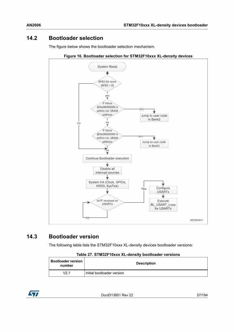
DocID13801 Rev 22 57/194
AN2606 STM32F10xxx XL-density devices bootloader
193
14.2 Bootloader selection
The figure below shows the bootloader selection mechanism.
Figure 16. Bootloader selection for STM32F10xxx XL-density devices
14.3 Bootloader version
The following table lists the STM32F10xxx XL-density devices bootloader versions:
Table 27. STM32F10xxx XL-density bootloader versions
Bootloader version number
Description
V2.1 Initial bootloader version

STM32F2xxxx devices bootloader AN2606
58/194 DocID13801 Rev 22
15 STM32F2xxxx devices bootloader
Two bootloader versions are available on STM32F2xxxx devices:
• V2.x supporting USART1 and USART3
This version is embedded in STM32F2xxxx devices revision B.
• V3.x supporting USART1, USART3, CAN2 and DFU (USB FS Device)
This version is embedded in STM32F2xxxx devices revision X and Y.
15.1 Bootloader V2.x
15.1.1 Bootloader configuration
The STM32F2xxxx bootloader is activated by applying pattern1 (described in Table 2: Bootloader activation patterns). The following table shows the hardware resources used by this bootloader.
Table 28. STM32F2xxxx configuration in system memory boot mode
Bootloader Feature/Peripheral State Comment
Common to all
bootloaders
RCC HSI enabled The system clock frequency is 24 MHz.
RAM -8 Kbytes starting from address 0x2000 0000.
System memory -30688 bytes starting from address 0x1FFF 0000 contain the bootloader firmware.
IWDG -
The independent watchdog (IWDG) prescaler is configured to its maximum value and is periodically refreshed to prevent watchdog reset (in case the hardware IWDG option was previously enabled by the user).
Power -
Voltage range is set to [1.62 V, 2.1 V]. In this range internal Flash write operations are allowed only in byte format (Half-Word, Word and Double-Word operations are not allowed). The voltage range can be configured in run time using bootloader commands.
USART1
bootloader
USART1 EnabledOnce initialized, the USART1 configuration is: 8 bits, even parity and 1 Stop bit.
USART1_RX pin Input PA10 pin: USART1 in reception mode
USART1_TX pin Output PA9 pin: USART1 in transmission mode
USART3
bootloader (on
PC10/PC11)
USART3 EnabledOnce initialized, the USART3 configuration is: 8 bits, even parity and 1 Stop bit.
USART3_RX pin Input PC11 pin: USART3 in reception mode
USART3_TX pin Output PC10 pin: USART3 in transmission mode

DocID13801 Rev 22 59/194
AN2606 STM32F2xxxx devices bootloader
193
The system clock is derived from the embedded internal high-speed RC. No external quartz is required for the bootloader code.
15.1.2 Bootloader selection
The figure below shows the bootloader selection mechanism.
Figure 17. Bootloader V2.x selection for STM32F2xxxx devices
USART3
bootloader (on
PB10/PB11)
USART3 EnabledOnce initialized, the USART3 configuration is: 8 bits, even parity and 1 Stop bit
USART3_RX pin Input PB11 pin: USART3 in reception mode
USART3_TX pin Output PB10 pin: USART3 in transmission mode
USART1 and
USART3
bootloaders
SysTick timer EnabledUsed to automatically detect the serial baud rate from the host.
Table 28. STM32F2xxxx configuration in system memory boot mode (continued)
Bootloader Feature/Peripheral State Comment
STM32F2xxxx devices bootloader AN2606
60/194 DocID13801 Rev 22
15.1.3 Bootloader version
This following table lists the STM32F2xxxx devices V2.x bootloader versions:
Table 29. STM32F2xxxx bootloader V2.x versions
Bootloader version number
Description Known limitations
V2.0 Initial V2.x bootloader version
When a Read Memory command or Write Memory command is issued with an unsupported memory address and a correct address checksum (ie. address 0x6000 0000), the command is aborted by the bootloader device, but the NACK (0x1F) is not sent to the host. As a result, the next 2 bytes (which are the number of bytes to be read/written and its checksum) are considered as a new command and its checksum. For the CAN interface, the Write Unprotect command is not functional. Instead you can use Write Memory command and write directly to the option bytes in order to disable the write protection.(1)
1. If the “number of data - 1” (N-1) to be read/written is not equal to a valid command code (0x00, 0x01, 0x02, 0x11, 0x21, 0x31, 0x43, 0x44, 0x63, 0x73, 0x82 or 0x92), then the limitation is not perceived from the host since the command is NACKed anyway (as an unsupported new command).

DocID13801 Rev 22 61/194
AN2606 STM32F2xxxx devices bootloader
193
15.2 Bootloader V3.x
15.2.1 Bootloader configuration
The STM32F2xxxx bootloader is activated by applying pattern1 (described in Table 2: Bootloader activation patterns). The following table shows the hardware resources used by this bootloader.
Table 30. STM32F2xxxx configuration in system memory boot mode
Bootloader Feature/Peripheral State Comment
Common to all bootloaders
RCC
HSI enabled
The system clock frequency is 24 MHz using the PLL.
The HSI clock source is used at startup (interface detection phase) and when USARTx interfaces are selected (once CAN or DFU bootloader is selected, the clock source will be derived from the external crystal).
HSE enabled
The system clock frequency is 60 MHz.
The HSE clock source is used only when the CAN or the DFU (USB FS Device) interfaces are selected.
The external clock must provide a frequency multiple of 1 MHz and ranging from 4 MHz to 26 MHz.
-
The Clock Security System (CSS) interrupt is enabled for the CAN and DFU bootloaders. Any failure (or removal) of the external clock generates system reset.
RAM -8 Kbytes starting from address 0x20000000 are used by the bootloader firmware.
System memory -30688 bytes starting from address 0x1FF0 0000 contain the bootloader firmware.
IWDG -
The independent watchdog (IWDG) prescaler is configured to its maximum value. It is periodically refreshed to prevent watchdog reset (in case the hardware IWDG option was previously enabled by the user).
Power -
Voltage range is set to [1.62 V, 2.1 V]. In this range internal Flash write operations are allowed only in byte format (Half-Word, Word and Double-Word operations are not allowed). The voltage range can be configured in run time using bootloader commands.

STM32F2xxxx devices bootloader AN2606
62/194 DocID13801 Rev 22
The system clock is derived from the embedded internal high-speed RC for USARTx bootloaders. This internal clock is also used for CAN and DFU (USB FS Device) but only for the selection phase. An external clock multiple of 1 MHz (between 4 and 26 MHz) is required for CAN and DFU bootloader execution after the selection phase.
USART1 bootloader
USART1 EnabledOnce initialized, the USART1 configuration is: 8 bits, even parity and 1 Stop bit.
USART1_RX pin Input PA10 pin: USART1 in reception mode
USART1_TX pin Output PA9 pin: USART1 in transmission mode
USART3 bootloader (on PB10/PB11)
USART3 EnabledOnce initialized, the USART3 configuration is: 8 bits, even parity and 1 Stop bit.
USART3_RX pin Input PB11 pin: USART3 in reception mode
USART3_TX pin Output PB10 pin: USART3 in transmission mode
USART3 bootloader (on PC10/PC11)
USART3 EnabledOnce initialized, the USART3 configuration is: 8 bits, even parity and 1 Stop bit.
USART3_RX pin Input PC11 pin: USART3 in reception mode
USART3_TX pin Output PC10 pin: USART3 in transmission mode
USART1 and USART3 bootloaders
SysTick timer EnabledUsed to automatically detect the serial baud rate from the host for USARTx bootloaders.
CAN2 bootloader
CAN2 Enabled
Once initialized, the CAN2 configuration is: Baudrate 125 kbps, 11-bit identifier.
Note: CAN1 is clocked during CAN2 bootloader execution because CAN1 manages the communication between CAN2 and SRAM.
CAN2_RX pin Input PB5 pin: CAN2 in reception mode
CAN2_TX pin Output PB13 pin: CAN2 in transmission mode
DFU bootloader
USB EnabledUSB OTG FS configured in Forced Device mode
USB_DM pin
Input/Output
PA11: USB DM line.
USB_DP pinPA12: USB DP line
No external Pull-up resistor is required
CAN2 and DFU bootloaders
TIM11 Enabled
This timer is used to determine the value of the HSE. Once the HSE frequency is determined, the system clock is configured to 60 MHz using PLL and HSE.
Table 30. STM32F2xxxx configuration in system memory boot mode (continued)
Bootloader Feature/Peripheral State Comment

DocID13801 Rev 22 63/194
AN2606 STM32F2xxxx devices bootloader
193
15.2.2 Bootloader selection
The figure below shows the bootloader selection mechanism.
Figure 18. Bootloader V3.x selection for STM32F2xxxx devices
STM32F2xxxx devices bootloader AN2606
64/194 DocID13801 Rev 22
15.2.3 Bootloader version
The following table lists the STM32F2xxxx devices V3.x bootloader versions:
Table 31. STM32F2xxxx bootloader V3.x versions
Bootloader version number
Description Known limitations
V3.2 Initial V3.x bootloader version.
– When a Read Memory command or Write Memory command is issued with an unsupported memory address and a correct address checksum (ie. address 0x6000 0000), the command is aborted by the bootloader device, but the NACK (0x1F) is not sent to the host. As a result, the next 2 bytes (which are the number of bytes to be read/written and its checksum) are considered as a new command and its checksum(1).
– Option bytes, OTP and Device Feature descriptors (in DFU interface) are set to “g” instead of “e” (not erasable memory areas).
1. If the “number of data - 1” (N-1) to be read/written is not equal to a valid command code (0x00, 0x01, 0x02, 0x11, 0x21, 0x31, 0x43, 0x44, 0x63, 0x73, 0x82 or 0x92), then the limitation is not perceived from the host since the command is NACKed anyway (as an unsupported new command).
V3.3Fix V3.2 limitations. DFU interface robustness enhancement.
– For the USART interface, two consecutive NACKs (instead of 1 NACK) are sent when a Read Memory or Write Memory command is sent and the RDP level is active.
– For the CAN interface, the Write Unprotect command is not functional. Instead you can use Write Memory command and write directly to the option bytes in order to disable the write protection.
DocID13801 Rev 22 65/194
AN2606 STM32F301xx/302x4(6/8) devices bootloader
193
16 STM32F301xx/302x4(6/8) devices bootloader
16.1 Bootloader configuration
The STM32F301xx/302x4(6/8) bootloader is activated by applying pattern2 (described in Table 2: Bootloader activation patterns). The following table shows the hardware resources used by this bootloader.
Table 32. STM32F301xx/302x4(6/8) configuration in system memory boot mode
Bootloader Feature/Peripheral State Comment
Common to all
bootloaders
RCC
HSI enabledThe system clock frequency is 48 MHz with HSI 48 MHz as clock source.
HSE enabled
The external clock can be used for all
bootloader interfaces and should have one
the following values 24, 18,16, 12, 9, 8, 6, 4, 3 MHz.
The PLL is used to generate the USB
48 MHz clock and the 48 MHz clock for the
system clock.
-
The Clock Security System (CSS) interrupt is
enabled for the DFU bootloader. Any failure
(or removal) of the external clock generates
system reset.
RAM -6 Kbytes starting from address 0x20000000 are used by the bootloader firmware
System memory -8 Kbytes starting from address 0x1FFFD800, contain the bootloader firmware
IWDG -
The independent watchdog (IWDG) prescaler is configured to its maximum value. It is periodically refreshed to prevent watchdog reset (in case the hardware IWDG option was previously enabled by the user).
USART1
bootloader
USART1 EnabledOnce initialized the USART1 configuration is: 8-bits, even parity and 1 Stop bit
USART1_RX pin Input PA10 pin: USART1 in reception mode
USART1_TX pin Output PA9 pin: USART1 in transmission mode
USART2
bootloader
USART2 EnabledOnce initialized the USART2 configuration is: 8-bits, even parity and 1 Stop bit
USART2_RX pin Input PA3 pin: USART2 in reception mode
USART2_TX pin Output PA2 pin: USART2 in transmission mode
USART1 and
USART2
bootloaders
SysTick timer EnabledUsed to automatically detect the serial baud rate from the host for USARTx bootloaders.

STM32F301xx/302x4(6/8) devices bootloader AN2606
66/194 DocID13801 Rev 22
The bootloader has two case of operation depending on the presence of the external clock (HSE) at bootloader startup:
• If HSE is present and has a value of 24, 18, 16, 12, 9, 8, 6, 4 or 3 MHz, the system clock is configured to 48 MHz with HSE as clock source. The DFU interface, USART1 and USART2 are functional and can be used to communicate with the bootloader device.
• If HSE is not present, the HSI is kept as default clock source and only USART1 and USART2 are functional.
The external clock (HSE) must be kept if it’s connected at bootloader startup because it will be used as system clock source.
DFU bootloader
USB Enabled USB used in FS mode
USB_DM pin
Input/Output
PA11: USB DM line.
USB_DP pinPA12: USB DP line
An external pull-up resistor 1.5 KOhm must be connected to USB_DP pin.
Table 32. STM32F301xx/302x4(6/8) configuration in system memory boot mode (continued)
Bootloader Feature/Peripheral State Comment

DocID13801 Rev 22 67/194
AN2606 STM32F301xx/302x4(6/8) devices bootloader
193
16.2 Bootloader selection
The figure below shows the bootloader selection mechanism.
Figure 19. Bootloader selection for STM32F301xx/302x4(6/8)
16.3 Bootloader version
The following table lists the STM32F301xx/302x4(6/8) devices bootloader versions:
Table 33. STM32F301xx/302x4(6/8) bootloader versions
Bootloader version number
Description Known limitations
V4.0 Initial bootloader version None
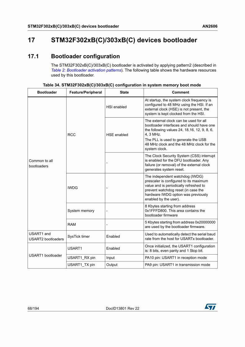
STM32F302xB(C)/303xB(C) devices bootloader AN2606
68/194 DocID13801 Rev 22
17 STM32F302xB(C)/303xB(C) devices bootloader
17.1 Bootloader configuration
The STM32F302xB(C)/303xB(C) bootloader is activated by applying pattern2 (described in Table 2: Bootloader activation patterns). The following table shows the hardware resources used by this bootloader.
Table 34. STM32F302xB(C)/303xB(C) configuration in system memory boot mode
Bootloader Feature/Peripheral State Comment
Common to all
bootloaders
RCC
HSI enabled
At startup, the system clock frequency is configured to 48 MHz using the HSI. If an external clock (HSE) is not present, the system is kept clocked from the HSI.
HSE enabled
The external clock can be used for all bootloader interfaces and should have one the following values 24, 18,16, 12, 9, 8, 6, 4, 3 MHz.
The PLL is used to generate the USB 48 MHz clock and the 48 MHz clock for the system clock.
-
The Clock Security System (CSS) interrupt is enabled for the DFU bootloader. Any failure (or removal) of the external clock generates system reset.
IWDG -
The independent watchdog (IWDG) prescaler is configured to its maximum value and is periodically refreshed to prevent watchdog reset (in case the hardware IWDG option was previously enabled by the user).
System memory -8 Kbytes starting from address 0x1FFFD800. This area contains the bootloader firmware
RAM -5 Kbytes starting from address 0x20000000 are used by the bootloader firmware.
USART1 and
USART2 bootloadersSysTick timer Enabled
Used to automatically detect the serial baud rate from the host for USARTx bootloader.
USART1 bootloader
USART1 EnabledOnce initialized, the USART1 configuration is: 8 bits, even parity and 1 Stop bit.
USART1_RX pin Input PA10 pin: USART1 in reception mode
USART1_TX pin Output PA9 pin: USART1 in transmission mode

DocID13801 Rev 22 69/194
AN2606 STM32F302xB(C)/303xB(C) devices bootloader
193
The bootloader has two case of operation depending on the presence of the external clock (HSE) at bootloader startup:
• If HSE is present and has a value of 24, 18, 16, 12, 9, 8, 6, 4 or 3 MHz, the system clock is configured to 48 MHz with HSE as clock source. The DFU interface, USART1 and USART2 are functional and can be used to communicate with the bootloader device.
• If HSE is not present, the HSI is kept as default clock source and only USART1 and USART2 are functional.
The external clock (HSE) must be kept if it’s connected at bootloader startup because it will be used as system clock source.
USART2 bootloader
USART2 EnabledOnce initialized, the USART2 configuration is: 8 bits, even parity and 1 Stop bit. The USART2 uses its remapped pins.
USART2_RX pin Input PD6 pin: USART2 in reception mode
USART2_TX pin Output PD5 pin: USART2 in transmission mode
DFU bootloader
USB Enabled USB used in FS mode
USB_DM pin
Input/Output
PA11: USB DM line.
USB_DP pinPA12: USB DP line
An external pull-up resistor 1.5 KOhm must be connected to USB_DP pin.
Table 34. STM32F302xB(C)/303xB(C) configuration in system memory boot mode (continued)
Bootloader Feature/Peripheral State Comment

STM32F302xB(C)/303xB(C) devices bootloader AN2606
70/194 DocID13801 Rev 22
17.2 Bootloader selection
The figure below shows the bootloader selection mechanism.
Figure 20. Bootloader selection for STM32F302xB(C)/303xB(C) devices
17.3 Bootloader version
The following table lists the STM32F302xB(C)/303xB(C) devices bootloader versions.
Table 35. STM32F302xB(C)/303xB(C) bootloader versions
Bootloader version number Description Known limitations
V4.1 Initial bootloader version None

DocID13801 Rev 22 71/194
AN2606 STM32F302xD(E)/303xD(E) devices bootloader
193
18 STM32F302xD(E)/303xD(E) devices bootloader
18.1 Bootloader configuration
TThe STM32F302xD(E)/303xD(E) bootloader is activated by applying pattern2 (described in Table 2: Bootloader activation patterns). The following table shows the hardware resources used by this bootloader.
Table 36.STM32F302xD(E)/303xD(E) configuration in system memory boot mode
Bootloader Feature/Peripheral State Comment
Common to all bootloaders
RCC
HSI enabledThe system clock frequency is 48 MHz with HSI 48 MHz as clock source.
HSE enabled
The external clock can be used for all bootloader interfaces and should have one the following values 24, 18,16, 12, 9, 8, 6, 4, 3 MHz. The PLL is used to generate the USB 48 MHz clock and the 48 MHz clock for the system clock.
-The Clock Security System (CSS) interrupt is enabled for the DFU bootloader. Any failure (or removal) of the external clock generates system reset.
RAM -6 Kbytes starting from address 0x20000000 are used by the bootloader firmware
System memory -8 Kbytes starting from address 0x1FFFD800, contain the bootloader firmware
IWDG -
The independent watchdog (IWDG) prescaler is configured to its maximum value. It is periodically refreshed to prevent watchdog reset (in case the hardware IWDG option was previously enabled by the user).
USART1 bootloader
USART1 EnabledOnce initialized the USART1 configuration is: 8-bits, even parity and 1 Stop bit
USART1_RX pin Input PA10 pin: USART1 in reception mode
USART1_TX pin Output PA9 pin: USART1 in transmission mode
USART2 bootloader
USART2 EnabledOnce initialized the USART2 configuration is: 8-bits, even parity and 1 Stop bit
USART2_RX pin Input PA3 pin: USART2 in reception mode
USART2_TX pin Output PA2 pin: USART2 in transmission mode
USART1 and USART2 bootloaders
SysTick timer EnabledUsed to automatically detect the serial baud rate from the host for USARTx bootloaders.
DFU bootloader
USB EnabledUSB FS configured in Forced Device mode. USB FS interrupt vector is enabled and used for USB DFU communications.
USB_DM pin
Input/Output
PA11 pin: USB FS DM line.
USB_DP pinPA12 pin: USB FS DP line. An external pull-up resistor 1.5 KOhm must be connected to USB_DP pin.
STM32F302xD(E)/303xD(E) devices bootloader AN2606
72/194 DocID13801 Rev 22
The bootloader has two cases of operation depending on the presence of the external clock (HSE) at bootloader startup:
• If HSE is present and has a value of 24, 18, 16, 12, 9, 8, 6, 4 or 3 MHz, the system clock is configured to 48 MHz with HSE as clock source. The DFU interface, USART1 and USART2 are functional and can be used to communicate with the bootloader device.
• If HSE is not present, the HSI is kept as default clock source and only USART1 and USART2 are functional.
The external clock (HSE) must be kept if it’s connected at bootloader startup because it will be used as system clock source.
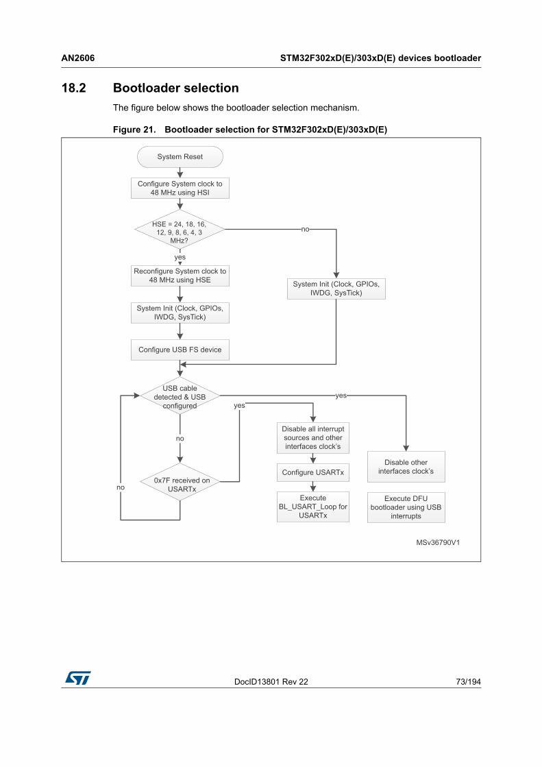
DocID13801 Rev 22 73/194
AN2606 STM32F302xD(E)/303xD(E) devices bootloader
193
18.2 Bootloader selection
The figure below shows the bootloader selection mechanism.
Figure 21. Bootloader selection for STM32F302xD(E)/303xD(E)
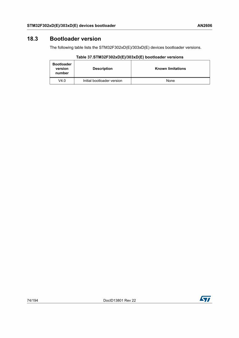
STM32F302xD(E)/303xD(E) devices bootloader AN2606
74/194 DocID13801 Rev 22
18.3 Bootloader version
The following table lists the STM32F302xD(E)/303xD(E) devices bootloader versions.
Table 37.STM32F302xD(E)/303xD(E) bootloader versions
Bootloader version number
Description Known limitations
V4.0 Initial bootloader version None
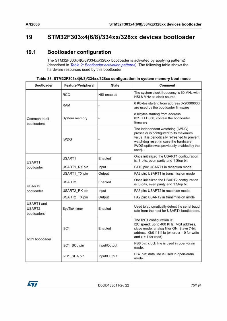
DocID13801 Rev 22 75/194
AN2606 STM32F303x4(6/8)/334xx/328xx devices bootloader
193
19 STM32F303x4(6/8)/334xx/328xx devices bootloader
19.1 Bootloader configuration
The STM32F303x4(6/8)/334xx/328xx bootloader is activated by applying pattern2 (described in Table 2: Bootloader activation patterns). The following table shows the hardware resources used by this bootloader.
Table 38. STM32F303x4(6/8)/334xx/328xx configuration in system memory boot mode
Bootloader Feature/Peripheral State Comment
Common to all
bootloaders
RCC HSI enabledThe system clock frequency is 60 MHz with HSI 8 MHz as clock source.
RAM -6 Kbytes starting from address 0x20000000 are used by the bootloader firmware
System memory -8 Kbytes starting from address 0x1FFFD800, contain the bootloader firmware
IWDG -
The independent watchdog (IWDG) prescaler is configured to its maximum value. It is periodically refreshed to prevent watchdog reset (in case the hardware IWDG option was previously enabled by the user).
USART1
bootloader
USART1 EnabledOnce initialized the USART1 configuration is: 8-bits, even parity and 1 Stop bit
USART1_RX pin Input PA10 pin: USART1 in reception mode
USART1_TX pin Output PA9 pin: USART1 in transmission mode
USART2
bootloader
USART2 EnabledOnce initialized the USART2 configuration is: 8-bits, even parity and 1 Stop bit
USART2_RX pin Input PA3 pin: USART2 in reception mode
USART2_TX pin Output PA2 pin: USART2 in transmission mode
USART1 and
USART2
bootloaders
SysTick timer EnabledUsed to automatically detect the serial baud rate from the host for USARTx bootloaders.
I2C1 bootloader
I2C1 Enabled
The I2C1 configuration is: I2C speed: up to 400 KHz, 7-bit address, slave mode, analog filter ON. Slave 7-bit address: 0b0111111x (where x = 0 for write and x = 1 for read)
I2C1_SCL pin Input/OutputPB6 pin: clock line is used in open-drain mode.
I2C1_SDA pin Input/OutputPB7 pin: data line is used in open-drain mode.

STM32F303x4(6/8)/334xx/328xx devices bootloader AN2606
76/194 DocID13801 Rev 22
The system clock is derived from the embedded internal high-speed RC, no external quartz is required for the bootloader execution.
19.2 Bootloader selection
The figure below shows the bootloader selection mechanism.
Figure 22. Bootloader selection for STM32F303x4(6/8)/334xx/328xx
19.3 Bootloader version
The following table lists the STM32F303x4(6/8)/334xx/328xx devices bootloader versions:
Table 39. STM32F303x4(6/8)/334xx/328xx bootloader versions
Bootloader version number
Description Known limitations
V5.0 Initial bootloader version None
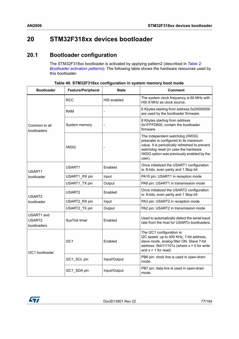
DocID13801 Rev 22 77/194
AN2606 STM32F318xx devices bootloader
193
20 STM32F318xx devices bootloader
20.1 Bootloader configuration
The STM32F318xx bootloader is activated by applying pattern2 (described in Table 2: Bootloader activation patterns). The following table shows the hardware resources used by this bootloader.
Table 40. STM32F318xx configuration in system memory boot mode
Bootloader Feature/Peripheral State Comment
Common to all
bootloaders
RCC HSI enabledThe system clock frequency is 60 MHz with HSI 8 MHz as clock source.
RAM -6 Kbytes starting from address 0x20000000 are used by the bootloader firmware
System memory -8 Kbytes starting from address 0x1FFFD800, contain the bootloader firmware
IWDG -
The independent watchdog (IWDG) prescaler is configured to its maximum value. It is periodically refreshed to prevent watchdog reset (in case the hardware IWDG option was previously enabled by the user).
USART1
bootloader
USART1 EnabledOnce initialized the USART1 configuration is: 8-bits, even parity and 1 Stop bit
USART1_RX pin Input PA10 pin: USART1 in reception mode
USART1_TX pin Output PA9 pin: USART1 in transmission mode
USART2
bootloader
USART2 EnabledOnce initialized the USART2 configuration is: 8-bits, even parity and 1 Stop bit
USART2_RX pin Input PA3 pin: USART2 in reception mode
USART2_TX pin Output PA2 pin: USART2 in transmission mode
USART1 and
USART2
bootloaders
SysTick timer EnabledUsed to automatically detect the serial baud rate from the host for USARTx bootloaders.
I2C1 bootloader
I2C1 Enabled
The I2C1 configuration is: I2C speed: up to 400 KHz, 7-bit address, slave mode, analog filter ON. Slave 7-bit address: 0b0111101x (where x = 0 for write and x = 1 for read)
I2C1_SCL pin Input/OutputPB6 pin: clock line is used in open-drain mode.
I2C1_SDA pin Input/OutputPB7 pin: data line is used in open-drain mode.

STM32F318xx devices bootloader AN2606
78/194 DocID13801 Rev 22
The system clock is derived from the embedded internal high-speed RC, no external quartz is required for the bootloader execution.
20.2 Bootloader selection
The figure below shows the bootloader selection mechanism.
Figure 23. Bootloader selection for STM32F318xx
I2C3 bootloader
I2C3 Enabled
The I2C3 configuration is:
I2C speed: up to 400 KHz, 7-bit address,slave mode, analog filter ON. Slave 7-bit address: 0b0111101x (where x = 0 for write and x = 1 for read) and digital filter disabled.
I2C3_SCL pin Input/OutputPA8 pin: clock line is used in open-drain mode.
I2C3_SDA pin Input/OutputPB5 pin: data line is used in open-drain mode.
Table 40. STM32F318xx configuration in system memory boot mode (continued)
Bootloader Feature/Peripheral State Comment

DocID13801 Rev 22 79/194
AN2606 STM32F318xx devices bootloader
193
20.3 Bootloader version
The following table lists the STM32F318xx devices bootloader versions:
Table 41. STM32F318xx bootloader versions
Bootloader version number
Description Known limitations
V5.0 Initial bootloader version None

STM32F358xx devices bootloader AN2606
80/194 DocID13801 Rev 22
21 STM32F358xx devices bootloader
21.1 Bootloader configuration
The STM32F358xx bootloader is activated by applying pattern2 (described in Table 2: Bootloader activation patterns). The following table shows the hardware resources used by this bootloader.
Table 42. STM32F358xx configuration in system memory boot mode
Bootloader Feature/Peripheral State Comment
Common to all
bootloaders
RCC HSI enabledThe system clock frequency is 8 MHz using the HSI.
IWDG -
The independent watchdog (IWDG) prescaler is configured to its maximum value and is periodically refreshed to prevent watchdog reset (in case the hardware IWDG option was previously enabled by the user). Window feature is disabled.
System memory -8 Kbytes starting from address 0x1FFFD800. This area contains the bootloader firmware.
RAM -5 Kbytes starting from address 0x20000000 are used by the bootloader firmware.
USART1
bootloader
USART1 EnabledOnce initialized, the USART1 configuration is: 8 bits, even parity and 1 Stop bit.
USART1_RX pin Input PA10 pin: USART1 in reception mode.
USART1_TX pin Output PA9 pin: USART1 in transmission mode.
USART2
bootloader
USART2 EnabledOnce initialized, the USART2 configuration is: 8 bits, even parity and 1 Stop bit. The USART2 uses its remapped pins.
USART2_RX pin Input PD6 pin: USART2 in reception mode.
USART2_TX pin Output PD5 pin: USART2 in transmission mode.
USART1 and
USART2
bootloaders
SysTick timer EnabledUsed to automatically detect the serial baud rate from the host for USARTx bootloader.
I2C1
bootloader
I2C1 Enabled
The I2C1 configuration is:
I2C speed: up to 400 KHz, 7-bit address, slave mode, analog filter ON. Slave 7-bit address: 0b0110111x (where x = 0 for write and x = 1 for read)
I2C1_SCL pin Input/ OutputPB6 pin: clock line is used in open-drain mode.
I2C1_SDA pin Input/ OutputPB7 pin: data line is used in open-drain mode.
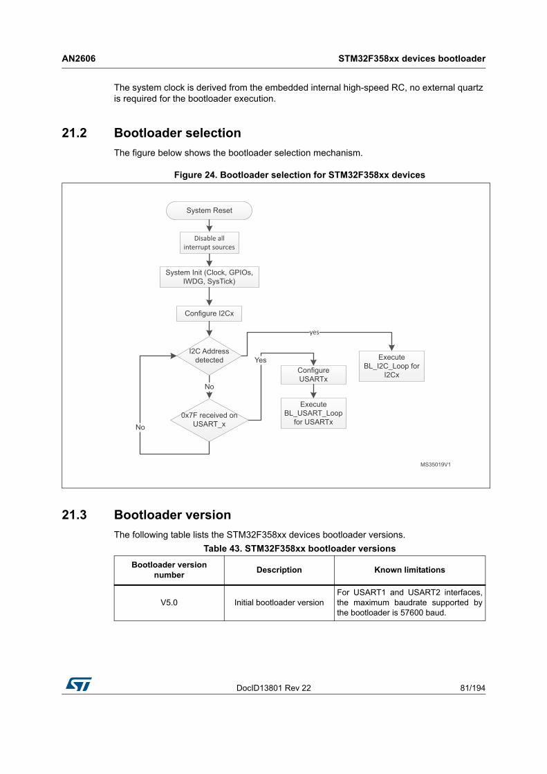
DocID13801 Rev 22 81/194
AN2606 STM32F358xx devices bootloader
193
The system clock is derived from the embedded internal high-speed RC, no external quartz is required for the bootloader execution.
21.2 Bootloader selection
The figure below shows the bootloader selection mechanism.
Figure 24. Bootloader selection for STM32F358xx devices
21.3 Bootloader version
The following table lists the STM32F358xx devices bootloader versions.
Initial bootloader version
Table 43. STM32F358xx bootloader versions
Bootloader version number
Description Known limitations
V5.0For USART1 and USART2 interfaces, the maximum baudrate supported by the bootloader is 57600 baud.
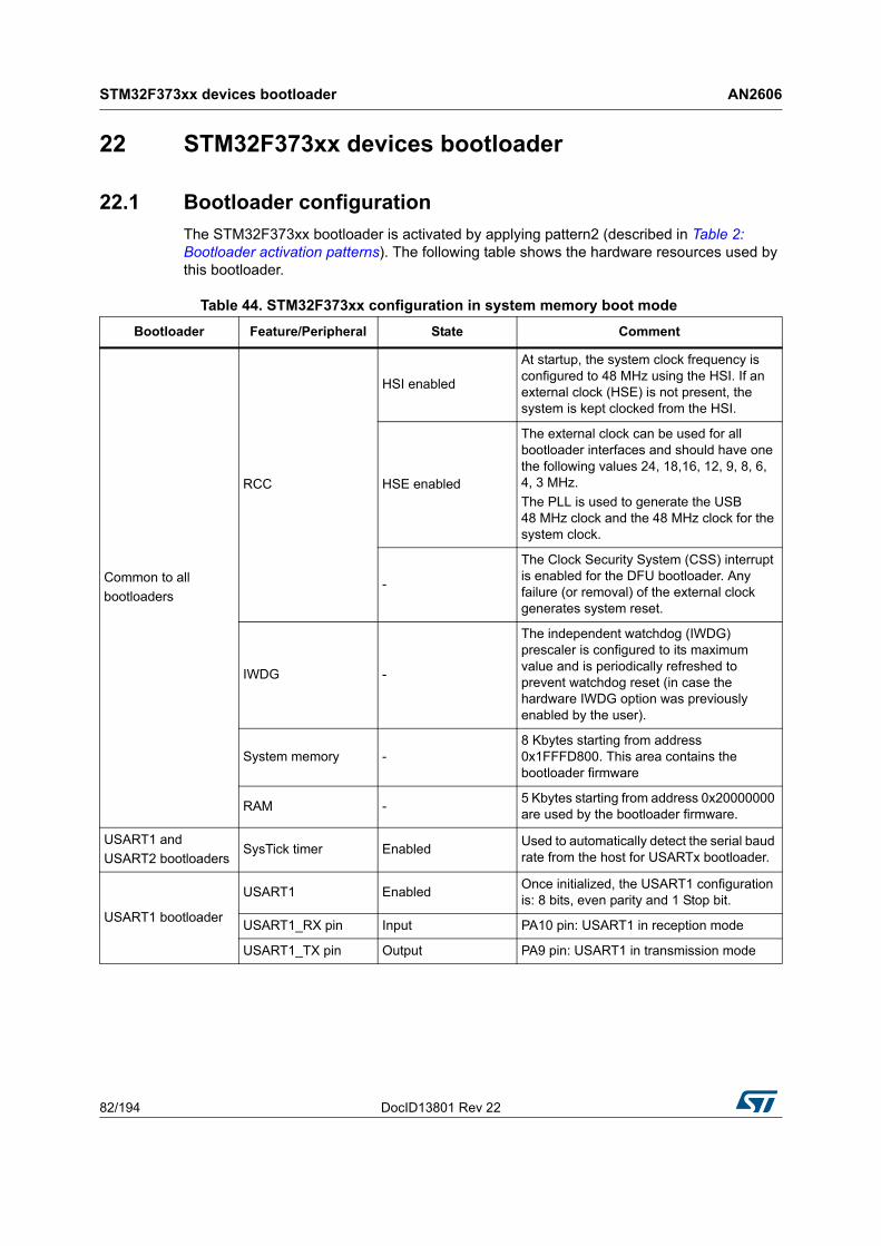
STM32F373xx devices bootloader AN2606
82/194 DocID13801 Rev 22
22 STM32F373xx devices bootloader
22.1 Bootloader configuration
The STM32F373xx bootloader is activated by applying pattern2 (described in Table 2: Bootloader activation patterns). The following table shows the hardware resources used by this bootloader.
Table 44. STM32F373xx configuration in system memory boot mode
Bootloader Feature/Peripheral State Comment
Common to all
bootloaders
RCC
HSI enabled
At startup, the system clock frequency is configured to 48 MHz using the HSI. If an external clock (HSE) is not present, the system is kept clocked from the HSI.
HSE enabled
The external clock can be used for all bootloader interfaces and should have one the following values 24, 18,16, 12, 9, 8, 6, 4, 3 MHz.
The PLL is used to generate the USB 48 MHz clock and the 48 MHz clock for the system clock.
-
The Clock Security System (CSS) interrupt is enabled for the DFU bootloader. Any failure (or removal) of the external clock generates system reset.
IWDG -
The independent watchdog (IWDG) prescaler is configured to its maximum value and is periodically refreshed to prevent watchdog reset (in case the hardware IWDG option was previously enabled by the user).
System memory -8 Kbytes starting from address 0x1FFFD800. This area contains the bootloader firmware
RAM -5 Kbytes starting from address 0x20000000 are used by the bootloader firmware.
USART1 and
USART2 bootloadersSysTick timer Enabled
Used to automatically detect the serial baud rate from the host for USARTx bootloader.
USART1 bootloader
USART1 EnabledOnce initialized, the USART1 configuration is: 8 bits, even parity and 1 Stop bit.
USART1_RX pin Input PA10 pin: USART1 in reception mode
USART1_TX pin Output PA9 pin: USART1 in transmission mode

DocID13801 Rev 22 83/194
AN2606 STM32F373xx devices bootloader
193
The bootloader has two case of operation depending on the presence of the external clock (HSE) at bootloader startup:
• If HSE is present and has a value of 24, 18, 16, 12, 9, 8, 6, 4 or 3 MHz, the system clock is configured to 48 MHz with HSE as clock source. The DFU interface, USART1 and USART2 are functional and can be used to communicate with the bootloader device.
• If HSE is not present, the HSI is kept as default clock source and only USART1 and USART2 are functional.
Note: The external clock (HSE) must be kept if it’s connected at bootloader startup because it will be used as system clock source.
USART2 bootloader
USART2 EnabledOnce initialized, the USART2 configuration is: 8 bits, even parity and 1 Stop bit. The USART2 uses its remapped pins.
USART2_RX pin Input PD6 pin: USART2 in reception mode
USART2_TX pin Output PD5 pin: USART2 in transmission mode
DFU bootloader
USB Enabled USB used in FS mode
USB_DM pin
Input/Output
PA11: USB DM line.
USB_DP pinPA12: USB DP line
An external pull-up resistor 1.5 KOhm must be connected to USB_DP pin.
Table 44. STM32F373xx configuration in system memory boot mode (continued)
Bootloader Feature/Peripheral State Comment

STM32F373xx devices bootloader AN2606
84/194 DocID13801 Rev 22
22.2 Bootloader selection
The figure below shows the bootloader selection mechanism.
Figure 25. Bootloader selection for STM32F373xx devices
22.3 Bootloader version
The following table lists the STM32F373xx devices bootloader versions.
Table 45. STM32F373xx bootloader versions
Bootloader version number Description Known limitations
V4.1 Initial bootloader version None

DocID13801 Rev 22 85/194
AN2606 STM32F378xx devices bootloader
193
23 STM32F378xx devices bootloader
23.1 Bootloader configuration
The STM32F378xx bootloader is activated by applying pattern2 (described in Table 2: Bootloader activation patterns). The following table shows the hardware resources used by this bootloader.
Table 46. STM32F378xx configuration in system memory boot mode
Bootloader Feature/Peripheral State Comment
Common to all
bootloaders
RCC HSI enabledThe system clock frequency is 8 MHz using the HSI.
IWDG -
The independent watchdog (IWDG) prescaler is configured to its maximum value and is periodically refreshed to prevent watchdog reset (in case the hardware IWDG option was previously enabled by the user). Window feature is disabled.
System memory -8 Kbytes starting from address 0x1FFFD800. This area contains the bootloader firmware
RAM -4 Kbytes starting from address 0x20000000 are used by the bootloader firmware.
USART1
bootloader
USART1 EnabledOnce initialized, the USART1 configuration is: 8 bits, even parity and 1 Stop bit
USART1_RX pin Input PA10 pin: USART1 in reception mode.
USART1_TX pin Output PA9 pin: USART1 in transmission mode.
USART2
bootloader
USART2 EnabledOnce initialized, the USART2 configuration is: 8 bits, even parity and 1 Stop bit. The USART2 uses its remapped pins.
USART2_RX pin Input PD6 pin: USART2 in reception mode.
USART2_TX pin Output PD5 pin: USART2 in transmission mode.
USART1 and
USART2
bootloaders
SysTick timer EnabledUsed to automatically detect the serial baud rate from the host for USARTx bootloader.
I2C1
bootloader
I2C1 Enabled
The I2C1 configuration is:
I2C speed: up to 400 KHz, 7-bit address, slave mode, analog filter ON. Slave 7-bit address: 0b0110111x (where x = 0 for write and x = 1 for read).
I2C1_SCL pin Input/ OutputPB6 pin: clock line is used in open-drain mode.
I2C1_SDA pin Input/ OutputPB7 pin: data line is used in open-drain mode.

STM32F378xx devices bootloader AN2606
86/194 DocID13801 Rev 22
The system clock is derived from the embedded internal high-speed RC, no external quartz is required for the bootloader execution.
23.2 Bootloader selection
The figure below shows the bootloader selection mechanism.
Figure 26. Bootloader selection for STM32F378xx devices
23.3 Bootloader version
The following table lists the STM32F378xx devices bootloader versions.
Initial bootloader version
Table 47. STM32F378xx bootloader versions
Bootloader version number
Description Known limitations
V5.0For USART1 and USART2 interfaces, the maximum baudrate supported by the bootloader is 57600 baud.

DocID13801 Rev 22 87/194
AN2606 STM32F398xx devices bootloader
193
24 STM32F398xx devices bootloader
24.1 Bootloader configuration
The STM32F398xx bootloader is activated by applying pattern2 (described in Table 2: Bootloader activation patterns). The following table shows the hardware resources used by this bootloader.
Table 48.STM32F398xx configuration in system memory boot mode
Bootloader Feature/Peripheral State Comment
Common to all
bootloaders
RCC HSI enabledThe system clock frequency is 60 MHz with HSI 8 MHz as clock source.
RAM -6 Kbytes starting from address 0x20000000 are used by the bootloader firmware
System memory -7 Kbytes starting from address 0x1FFFD800, contain the bootloader firmware
IWDG -
The independent watchdog (IWDG) prescaler is configured to its maximum value. It is periodically refreshed to prevent watchdog reset (in case the hardware IWDG option was previously enabled by the user).
USART1
bootloader
USART1 EnabledOnce initialized the USART1 configuration is: 8-bits, even parity and 1 Stop bit
USART1_RX pin Input PA10 pin: USART1 in reception mode
USART1_TX pin Output PA9 pin: USART1 in transmission mode
USART2
bootloader
USART2 EnabledOnce initialized the USART2 configuration is: 8-bits, even parity and 1 Stop bit
USART2_RX pin Input PA3 pin: USART2 in reception mode
USART2_TX pin Output PA2 pin: USART2 in transmission mode
USART1 and USART2
bootloadersSysTick timer Enabled
Used to automatically detect the serial baud rate from the host for USARTx bootloaders.
I2C1 bootloader
I2C1 Enabled
The I2C1 configuration is:
I2C speed: up to 400 KHz, 7-bit address, slave mode, analog filter ON. Slave 7-bit address: 0b1000000x (where x = 0 for write and x = 1 for read).
I2C1_SCL pin Input/Output PB6 pin: clock line is used in open-drain mode.
I2C1_SDA pin Input/Output PB7 pin: data line is used in open-drain mode.
I2C3 bootloader
I2C3 Enabled
The I2C3 configuration is:
I2C speed: up to 400 KHz, 7-bit address, slave mode, analog filter ON. Slave 7-bit address: 0b1000000x (where x = 0 for write and x = 1 for read).
I2C3_SCL pin Input/Output PA8 pin: clock line is used in open-drain mode.
I2C3_SDA pin Input/Output PB5 pin: data line is used in open-drain mode.

STM32F398xx devices bootloader AN2606
88/194 DocID13801 Rev 22
The system clock is derived from the embedded internal high-speed RC for all bootloader interfaces. No external quartz is required for bootloader operations.
24.2 Bootloader selection
The figure below shows the bootloader selection mechanism.
Figure 27.Bootloader selection for STM32F398xx
24.3 Bootloader version
The following table lists the STM32F398xx devices bootloader versions.
Table 49.STM32F398xx bootloader versions
Bootloader version number
Description Known limitations
V5.0 Initial bootloader version None
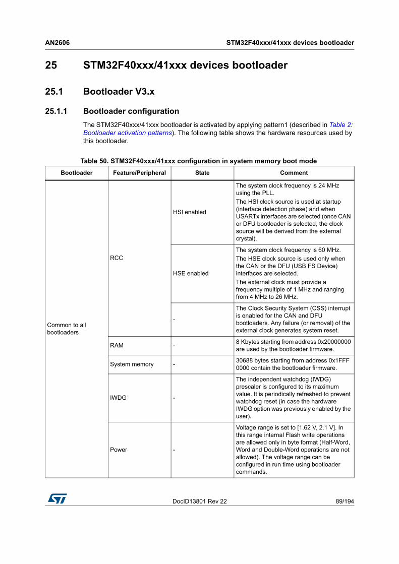
DocID13801 Rev 22 89/194
AN2606 STM32F40xxx/41xxx devices bootloader
193
25 STM32F40xxx/41xxx devices bootloader
25.1 Bootloader V3.x
25.1.1 Bootloader configuration
The STM32F40xxx/41xxx bootloader is activated by applying pattern1 (described in Table 2: Bootloader activation patterns). The following table shows the hardware resources used by this bootloader.
Table 50. STM32F40xxx/41xxx configuration in system memory boot mode
Bootloader Feature/Peripheral State Comment
Common to all bootloaders
RCC
HSI enabled
The system clock frequency is 24 MHz using the PLL.
The HSI clock source is used at startup (interface detection phase) and when USARTx interfaces are selected (once CAN or DFU bootloader is selected, the clock source will be derived from the external crystal).
HSE enabled
The system clock frequency is 60 MHz.
The HSE clock source is used only when the CAN or the DFU (USB FS Device) interfaces are selected.
The external clock must provide a frequency multiple of 1 MHz and ranging from 4 MHz to 26 MHz.
-
The Clock Security System (CSS) interrupt is enabled for the CAN and DFU bootloaders. Any failure (or removal) of the external clock generates system reset.
RAM -8 Kbytes starting from address 0x20000000 are used by the bootloader firmware.
System memory -30688 bytes starting from address 0x1FFF 0000 contain the bootloader firmware.
IWDG -
The independent watchdog (IWDG) prescaler is configured to its maximum value. It is periodically refreshed to prevent watchdog reset (in case the hardware IWDG option was previously enabled by the user).
Power -
Voltage range is set to [1.62 V, 2.1 V]. In this range internal Flash write operations are allowed only in byte format (Half-Word, Word and Double-Word operations are not allowed). The voltage range can be configured in run time using bootloader commands.
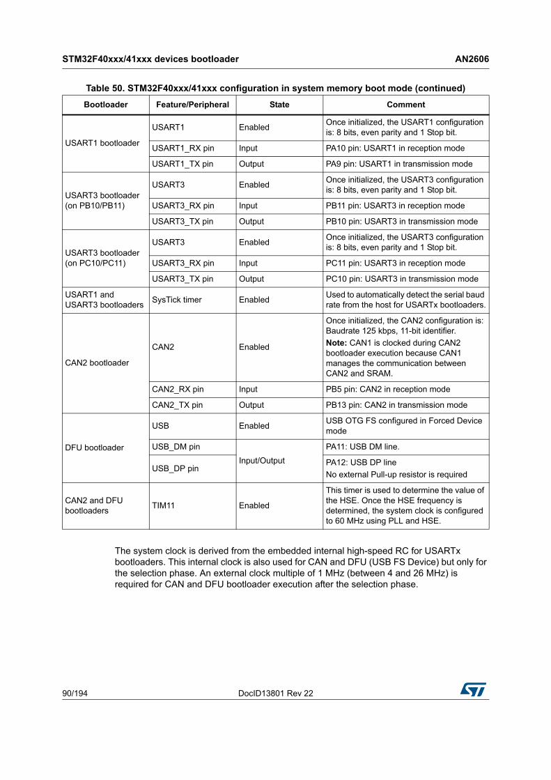
STM32F40xxx/41xxx devices bootloader AN2606
90/194 DocID13801 Rev 22
The system clock is derived from the embedded internal high-speed RC for USARTx bootloaders. This internal clock is also used for CAN and DFU (USB FS Device) but only for the selection phase. An external clock multiple of 1 MHz (between 4 and 26 MHz) is required for CAN and DFU bootloader execution after the selection phase.
USART1 bootloader
USART1 EnabledOnce initialized, the USART1 configuration is: 8 bits, even parity and 1 Stop bit.
USART1_RX pin Input PA10 pin: USART1 in reception mode
USART1_TX pin Output PA9 pin: USART1 in transmission mode
USART3 bootloader (on PB10/PB11)
USART3 EnabledOnce initialized, the USART3 configuration is: 8 bits, even parity and 1 Stop bit.
USART3_RX pin Input PB11 pin: USART3 in reception mode
USART3_TX pin Output PB10 pin: USART3 in transmission mode
USART3 bootloader (on PC10/PC11)
USART3 EnabledOnce initialized, the USART3 configuration is: 8 bits, even parity and 1 Stop bit.
USART3_RX pin Input PC11 pin: USART3 in reception mode
USART3_TX pin Output PC10 pin: USART3 in transmission mode
USART1 and USART3 bootloaders
SysTick timer EnabledUsed to automatically detect the serial baud rate from the host for USARTx bootloaders.
CAN2 bootloader
CAN2 Enabled
Once initialized, the CAN2 configuration is: Baudrate 125 kbps, 11-bit identifier.
Note: CAN1 is clocked during CAN2 bootloader execution because CAN1 manages the communication between CAN2 and SRAM.
CAN2_RX pin Input PB5 pin: CAN2 in reception mode
CAN2_TX pin Output PB13 pin: CAN2 in transmission mode
DFU bootloader
USB EnabledUSB OTG FS configured in Forced Device mode
USB_DM pin
Input/Output
PA11: USB DM line.
USB_DP pinPA12: USB DP line
No external Pull-up resistor is required
CAN2 and DFU bootloaders
TIM11 Enabled
This timer is used to determine the value of the HSE. Once the HSE frequency is determined, the system clock is configured to 60 MHz using PLL and HSE.
Table 50. STM32F40xxx/41xxx configuration in system memory boot mode (continued)
Bootloader Feature/Peripheral State Comment

DocID13801 Rev 22 91/194
AN2606 STM32F40xxx/41xxx devices bootloader
193
25.1.2 Bootloader selection
The figure below shows the bootloader selection mechanism.
Figure 28. Bootloader V3.x selection for STM32F40xxx/41xxx devices

STM32F40xxx/41xxx devices bootloader AN2606
92/194 DocID13801 Rev 22
25.1.3 Bootloader version
The following table lists the STM32F40xxx/41xxx devices V3.x bootloader versions:
Table 51. STM32F40xxx/41xxx bootloader V3.x versions
Bootloader version number
Description Known limitations
V3.0 Initial bootloader version
– When a Read Memory command or Write Memory command is issued with an unsupported memory address and a correct address checksum (ie. address 0x6000 0000), the command is aborted by the bootloader device, but the NACK (0x1F) is not sent to the host. As a result, the next 2 bytes (which are the number of bytes to be read/written and its checksum) are considered as a new command and its checksum(1).
– Option bytes, OTP and Device Feature descriptors (in DFU interface) are set to “g” instead of “e” (not erasable memory areas).
1. If the “number of data - 1” (N-1) to be read/written is not equal to a valid command code (0x00, 0x01, 0x02, 0x11, 0x21, 0x31, 0x43, 0x44, 0x63, 0x73, 0x82 or 0x92), then the limitation is not perceived from the host since the command is NACKed anyway (as an unsupported new command).
V3.1Fix V3.0 limitations. DFU interface robustness enhancement.
– For the USART interface, two consecutive NACKs (instead of 1 NACK) are sent when a Read Memory or Write Memory command is sent and the RDP level is active.
– For the CAN interface, the Write Unprotect command is not functional. Instead you can use Write Memory command and write directly to the option bytes in order to disable the write protection.

DocID13801 Rev 22 93/194
AN2606 STM32F401xB(C) devices bootloader
193
26 STM32F401xB(C) devices bootloader
26.1 Bootloader configuration
The STM32F401xB(C) bootloader is activated by applying pattern1 (described in Table 2: Bootloader activation patterns). The following table shows the hardware resources used by this bootloader.
Table 52. STM32F401xB(C) configuration in system memory boot mode
Bootloader Feature/Peripheral State Comment
Common to all
bootloaders
RCC
HSI enabled
The system clock frequency is 60 MHz using the PLL.
The HSI clock source is used at startup (interface detection phase) and when USART or SPI or I2C interfaces are selected (once DFU bootloader is selected, the clock source will be derived from the external crystal).
HSE enabled
The system clock frequency is 60 MHz.
The HSE clock source is used only when the DFU (USB FS Device) interfaces are selected.
The external clock must provide a frequency multiple of 1 MHz and ranging from 4 MHz to 26 MHz.
-
The Clock Security System (CSS) interrupt is enabled for the CAN and DFU bootloaders. Any failure (or removal) of the external clock generates system reset.
RAM -12 Kbytes starting from address 0x20000000 are used by the bootloader firmware
System memory -30424 bytes starting from address 0x1FFF0000, contain the bootloader firmware
IWDG -
The independent watchdog (IWDG) prescaler is configured to its maximum value. It is periodically refreshed to prevent watchdog reset (in case the hardware IWDG option was previously enabled by the user).
Power -
Voltage range is set to [1.62 V, 2.1 V]. In this range internal Flash write operations are allowed only in byte format (Half-Word, Word and Double-Word operations are not allowed). The voltage range can be configured in run time using bootloader commands.
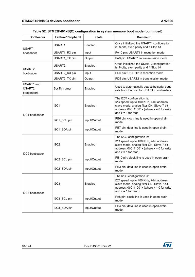
STM32F401xB(C) devices bootloader AN2606
94/194 DocID13801 Rev 22
USART1
bootloader
USART1 EnabledOnce initialized the USART1 configuration is: 8-bits, even parity and 1 Stop bit
USART1_RX pin Input PA10 pin: USART1 in reception mode
USART1_TX pin Output PA9 pin: USART1 in transmission mode
USART2
bootloader
USART2 EnabledOnce initialized the USART2 configuration is: 8-bits, even parity and 1 Stop bit
USART2_RX pin Input PD6 pin: USART2 in reception mode
USART2_TX pin Output PD5 pin: USART2 in transmission mode
USART1 and
USART2
bootloaders
SysTick timer EnabledUsed to automatically detect the serial baud rate from the host for USARTx bootloaders.
I2C1 bootloader
I2C1 Enabled
The I2C1 configuration is: I2C speed: up to 400 KHz, 7-bit address, slave mode, analog filter ON. Slave 7-bit address: 0b0111001x (where x = 0 for write and x = 1 for read)
I2C1_SCL pin Input/OutputPB6 pin: clock line is used in open-drain mode.
I2C1_SDA pin Input/OutputPB7 pin: data line is used in open-drain mode.
I2C2 bootloader
I2C2 Enabled
The I2C2 configuration is:
I2C speed: up to 400 KHz, 7-bit address, slave mode, analog filter ON. Slave 7-bit address: 0b0111001x (where x = 0 for write and x = 1 for read)
I2C2_SCL pin Input/OutputPB10 pin: clock line is used in open-drain mode.
I2C2_SDA pin Input/OutputPB3 pin: data line is used in open-drain mode.
I2C3 bootloader
I2C3 Enabled
The I2C3 configuration is:
I2C speed: up to 400 KHz, 7-bit address, slave mode, analog filter ON. Slave 7-bit address: 0b0111001x (where x = 0 for write and x = 1 for read)
I2C3_SCL pin Input/OutputPA8 pin: clock line is used in open-drain mode.
I2C3_SDA pin Input/OutputPB4 pin: data line is used in open-drain mode.
Table 52. STM32F401xB(C) configuration in system memory boot mode (continued)
Bootloader Feature/Peripheral State Comment
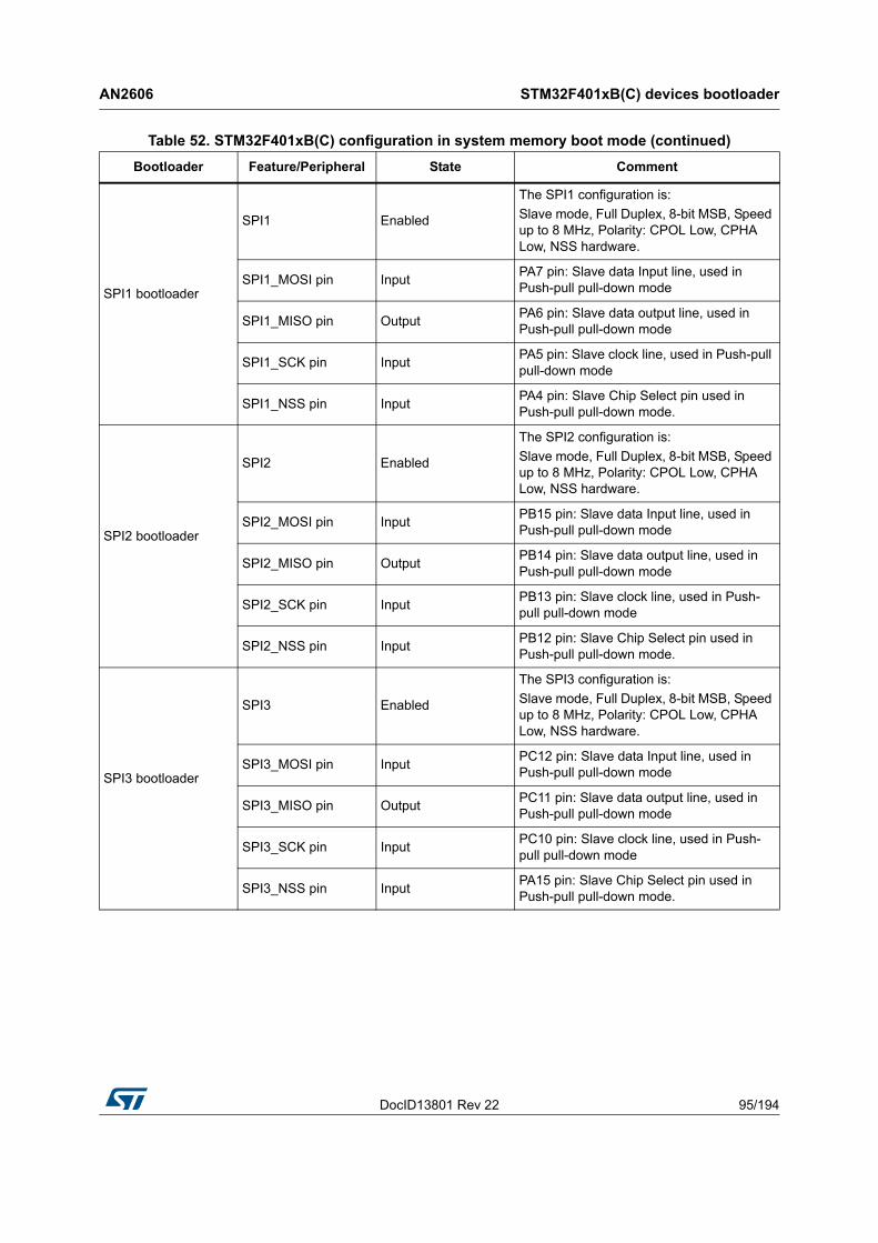
DocID13801 Rev 22 95/194
AN2606 STM32F401xB(C) devices bootloader
193
SPI1 bootloader
SPI1 Enabled
The SPI1 configuration is:
Slave mode, Full Duplex, 8-bit MSB, Speed up to 8 MHz, Polarity: CPOL Low, CPHA Low, NSS hardware.
SPI1_MOSI pin InputPA7 pin: Slave data Input line, used in Push-pull pull-down mode
SPI1_MISO pin OutputPA6 pin: Slave data output line, used in Push-pull pull-down mode
SPI1_SCK pin InputPA5 pin: Slave clock line, used in Push-pull pull-down mode
SPI1_NSS pin InputPA4 pin: Slave Chip Select pin used in Push-pull pull-down mode.
SPI2 bootloader
SPI2 Enabled
The SPI2 configuration is:
Slave mode, Full Duplex, 8-bit MSB, Speed up to 8 MHz, Polarity: CPOL Low, CPHA Low, NSS hardware.
SPI2_MOSI pin InputPB15 pin: Slave data Input line, used in Push-pull pull-down mode
SPI2_MISO pin OutputPB14 pin: Slave data output line, used in Push-pull pull-down mode
SPI2_SCK pin InputPB13 pin: Slave clock line, used in Push-pull pull-down mode
SPI2_NSS pin InputPB12 pin: Slave Chip Select pin used in Push-pull pull-down mode.
SPI3 bootloader
SPI3 Enabled
The SPI3 configuration is:
Slave mode, Full Duplex, 8-bit MSB, Speed up to 8 MHz, Polarity: CPOL Low, CPHA Low, NSS hardware.
SPI3_MOSI pin InputPC12 pin: Slave data Input line, used in Push-pull pull-down mode
SPI3_MISO pin OutputPC11 pin: Slave data output line, used in Push-pull pull-down mode
SPI3_SCK pin InputPC10 pin: Slave clock line, used in Push-pull pull-down mode
SPI3_NSS pin InputPA15 pin: Slave Chip Select pin used in Push-pull pull-down mode.
Table 52. STM32F401xB(C) configuration in system memory boot mode (continued)
Bootloader Feature/Peripheral State Comment
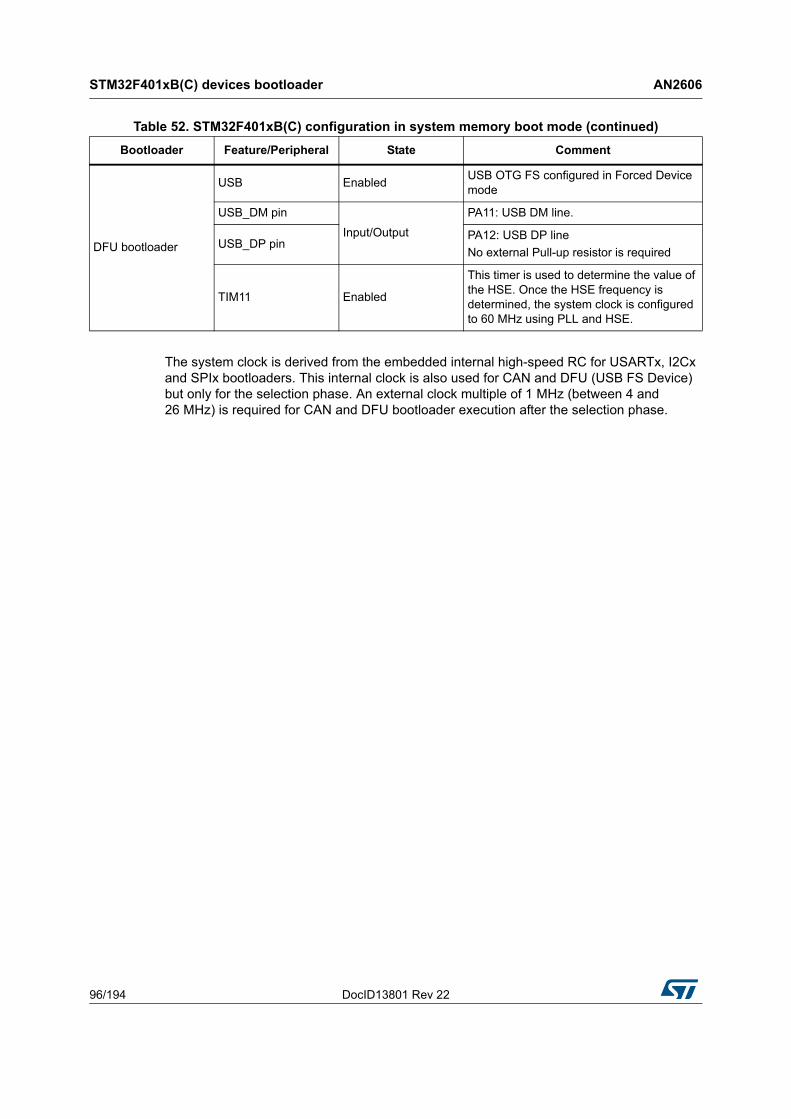
STM32F401xB(C) devices bootloader AN2606
96/194 DocID13801 Rev 22
The system clock is derived from the embedded internal high-speed RC for USARTx, I2Cx and SPIx bootloaders. This internal clock is also used for CAN and DFU (USB FS Device) but only for the selection phase. An external clock multiple of 1 MHz (between 4 and 26 MHz) is required for CAN and DFU bootloader execution after the selection phase.
DFU bootloader
USB EnabledUSB OTG FS configured in Forced Device mode
USB_DM pin
Input/Output
PA11: USB DM line.
USB_DP pinPA12: USB DP line
No external Pull-up resistor is required
TIM11 Enabled
This timer is used to determine the value of the HSE. Once the HSE frequency is determined, the system clock is configured to 60 MHz using PLL and HSE.
Table 52. STM32F401xB(C) configuration in system memory boot mode (continued)
Bootloader Feature/Peripheral State Comment
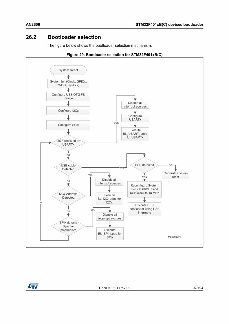
DocID13801 Rev 22 97/194
AN2606 STM32F401xB(C) devices bootloader
193
26.2 Bootloader selection
The figure below shows the bootloader selection mechanism.
Figure 29. Bootloader selection for STM32F401xB(C)

STM32F401xB(C) devices bootloader AN2606
98/194 DocID13801 Rev 22
26.3 Bootloader version
The following table lists the STM32F401xB(C) devices bootloader version.
Table 53. STM32F401xB(C) bootloader versions
Bootloader version number
Description Known limitations
V13.0 Initial bootloader version None
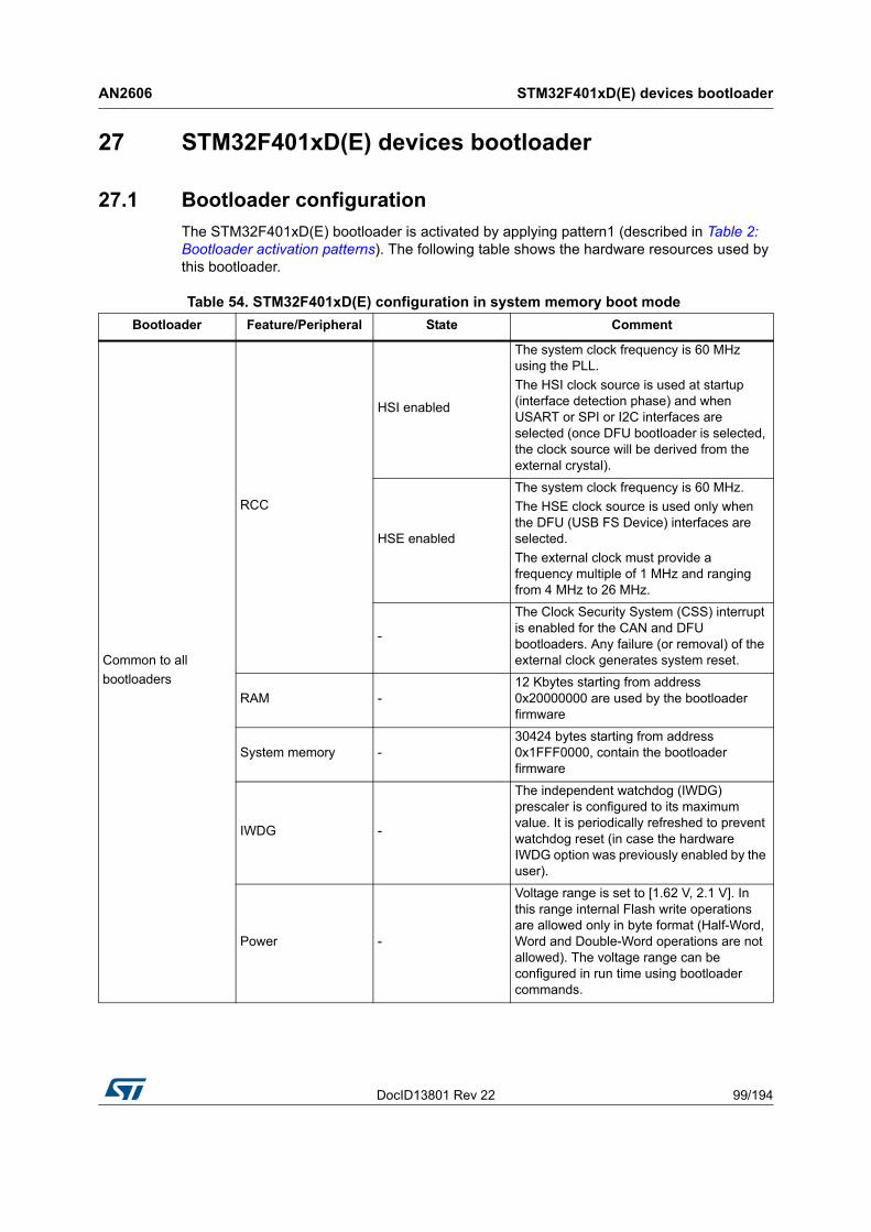
DocID13801 Rev 22 99/194
AN2606 STM32F401xD(E) devices bootloader
193
27 STM32F401xD(E) devices bootloader
27.1 Bootloader configuration
The STM32F401xD(E) bootloader is activated by applying pattern1 (described in Table 2: Bootloader activation patterns). The following table shows the hardware resources used by this bootloader.
Table 54. STM32F401xD(E) configuration in system memory boot mode
Bootloader Feature/Peripheral State Comment
Common to all
bootloaders
RCC
HSI enabled
The system clock frequency is 60 MHz using the PLL.
The HSI clock source is used at startup (interface detection phase) and when USART or SPI or I2C interfaces are selected (once DFU bootloader is selected, the clock source will be derived from the external crystal).
HSE enabled
The system clock frequency is 60 MHz.
The HSE clock source is used only when the DFU (USB FS Device) interfaces are selected.
The external clock must provide a frequency multiple of 1 MHz and ranging from 4 MHz to 26 MHz.
-
The Clock Security System (CSS) interrupt is enabled for the CAN and DFU bootloaders. Any failure (or removal) of the external clock generates system reset.
RAM -12 Kbytes starting from address 0x20000000 are used by the bootloader firmware
System memory -30424 bytes starting from address 0x1FFF0000, contain the bootloader firmware
IWDG -
The independent watchdog (IWDG) prescaler is configured to its maximum value. It is periodically refreshed to prevent watchdog reset (in case the hardware IWDG option was previously enabled by the user).
Power -
Voltage range is set to [1.62 V, 2.1 V]. In this range internal Flash write operations are allowed only in byte format (Half-Word, Word and Double-Word operations are not allowed). The voltage range can be configured in run time using bootloader commands.
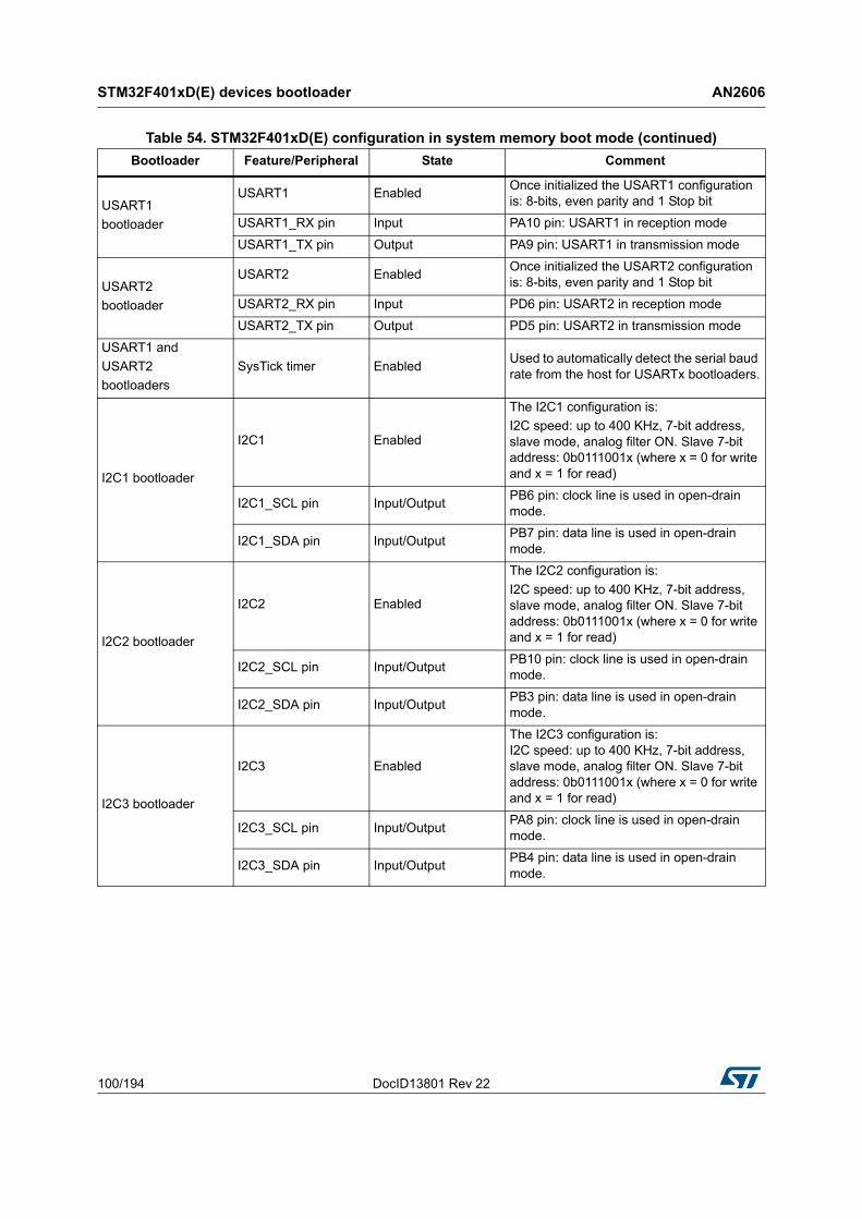
STM32F401xD(E) devices bootloader AN2606
100/194 DocID13801 Rev 22
USART1
bootloader
USART1 EnabledOnce initialized the USART1 configuration is: 8-bits, even parity and 1 Stop bit
USART1_RX pin Input PA10 pin: USART1 in reception mode
USART1_TX pin Output PA9 pin: USART1 in transmission mode
USART2
bootloader
USART2 EnabledOnce initialized the USART2 configuration is: 8-bits, even parity and 1 Stop bit
USART2_RX pin Input PD6 pin: USART2 in reception mode
USART2_TX pin Output PD5 pin: USART2 in transmission mode
USART1 and
USART2
bootloaders
SysTick timer EnabledUsed to automatically detect the serial baud rate from the host for USARTx bootloaders.
I2C1 bootloader
I2C1 Enabled
The I2C1 configuration is:
I2C speed: up to 400 KHz, 7-bit address, slave mode, analog filter ON. Slave 7-bit address: 0b0111001x (where x = 0 for write and x = 1 for read)
I2C1_SCL pin Input/OutputPB6 pin: clock line is used in open-drain mode.
I2C1_SDA pin Input/OutputPB7 pin: data line is used in open-drain mode.
I2C2 bootloader
I2C2 Enabled
The I2C2 configuration is:
I2C speed: up to 400 KHz, 7-bit address, slave mode, analog filter ON. Slave 7-bit address: 0b0111001x (where x = 0 for write and x = 1 for read)
I2C2_SCL pin Input/OutputPB10 pin: clock line is used in open-drain mode.
I2C2_SDA pin Input/OutputPB3 pin: data line is used in open-drain mode.
I2C3 bootloader
I2C3 Enabled
The I2C3 configuration is: I2C speed: up to 400 KHz, 7-bit address, slave mode, analog filter ON. Slave 7-bit address: 0b0111001x (where x = 0 for write and x = 1 for read)
I2C3_SCL pin Input/OutputPA8 pin: clock line is used in open-drain mode.
I2C3_SDA pin Input/OutputPB4 pin: data line is used in open-drain mode.
Table 54. STM32F401xD(E) configuration in system memory boot mode (continued)
Bootloader Feature/Peripheral State Comment
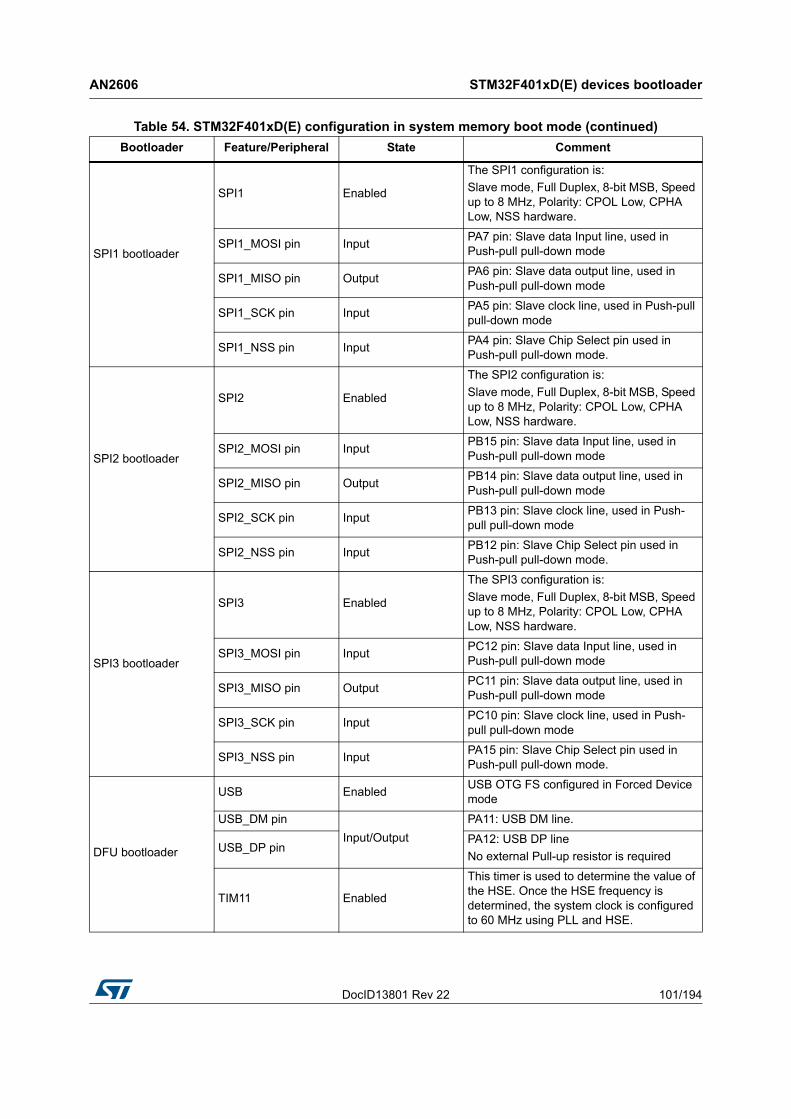
DocID13801 Rev 22 101/194
AN2606 STM32F401xD(E) devices bootloader
193
SPI1 bootloader
SPI1 Enabled
The SPI1 configuration is:
Slave mode, Full Duplex, 8-bit MSB, Speed up to 8 MHz, Polarity: CPOL Low, CPHA Low, NSS hardware.
SPI1_MOSI pin InputPA7 pin: Slave data Input line, used in Push-pull pull-down mode
SPI1_MISO pin OutputPA6 pin: Slave data output line, used in Push-pull pull-down mode
SPI1_SCK pin InputPA5 pin: Slave clock line, used in Push-pull pull-down mode
SPI1_NSS pin InputPA4 pin: Slave Chip Select pin used in Push-pull pull-down mode.
SPI2 bootloader
SPI2 Enabled
The SPI2 configuration is:
Slave mode, Full Duplex, 8-bit MSB, Speed up to 8 MHz, Polarity: CPOL Low, CPHA Low, NSS hardware.
SPI2_MOSI pin InputPB15 pin: Slave data Input line, used in Push-pull pull-down mode
SPI2_MISO pin OutputPB14 pin: Slave data output line, used in Push-pull pull-down mode
SPI2_SCK pin InputPB13 pin: Slave clock line, used in Push-pull pull-down mode
SPI2_NSS pin InputPB12 pin: Slave Chip Select pin used in Push-pull pull-down mode.
SPI3 bootloader
SPI3 Enabled
The SPI3 configuration is:
Slave mode, Full Duplex, 8-bit MSB, Speed up to 8 MHz, Polarity: CPOL Low, CPHA Low, NSS hardware.
SPI3_MOSI pin InputPC12 pin: Slave data Input line, used in Push-pull pull-down mode
SPI3_MISO pin OutputPC11 pin: Slave data output line, used in Push-pull pull-down mode
SPI3_SCK pin InputPC10 pin: Slave clock line, used in Push-pull pull-down mode
SPI3_NSS pin InputPA15 pin: Slave Chip Select pin used in Push-pull pull-down mode.
DFU bootloader
USB EnabledUSB OTG FS configured in Forced Device mode
USB_DM pin
Input/Output
PA11: USB DM line.
USB_DP pinPA12: USB DP line
No external Pull-up resistor is required
TIM11 Enabled
This timer is used to determine the value of the HSE. Once the HSE frequency is determined, the system clock is configured to 60 MHz using PLL and HSE.
Table 54. STM32F401xD(E) configuration in system memory boot mode (continued)
Bootloader Feature/Peripheral State Comment

STM32F401xD(E) devices bootloader AN2606
102/194 DocID13801 Rev 22
The system clock is derived from the embedded internal high-speed RC for USARTx, I2Cx and SPIx bootloaders. This internal clock is also used for CAN and DFU (USB FS Device) but only for the selection phase. An external clock multiple of 1 MHz (between 4 and 26 MHz) is required for CAN and DFU bootloader execution after the selection phase.
27.2 Bootloader selection
The figure below shows the bootloader selection mechanism.
Figure 30. Bootloader selection for STM32F401xD(E)

DocID13801 Rev 22 103/194
AN2606 STM32F401xD(E) devices bootloader
193
27.3 Bootloader version
The following table lists the STM32F401xD(E) devices bootloader version.
Table 55. STM32F401xD(E) bootloader versions
Bootloader version number
Description Known limitations
V13.1 Initial bootloader version None
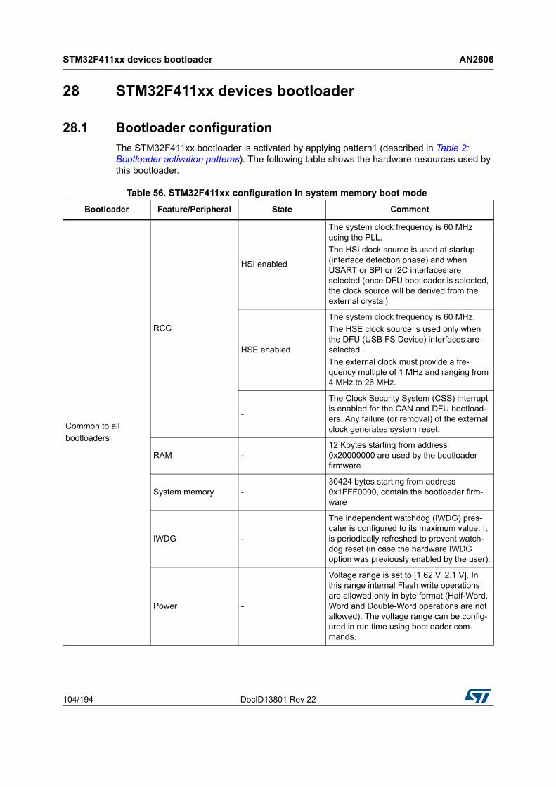
STM32F411xx devices bootloader AN2606
104/194 DocID13801 Rev 22
28 STM32F411xx devices bootloader
28.1 Bootloader configuration
The STM32F411xx bootloader is activated by applying pattern1 (described in Table 2: Bootloader activation patterns). The following table shows the hardware resources used by this bootloader.
Table 56. STM32F411xx configuration in system memory boot mode
Bootloader Feature/Peripheral State Comment
Common to all
bootloaders
RCC
HSI enabled
The system clock frequency is 60 MHz using the PLL.
The HSI clock source is used at startup (interface detection phase) and when USART or SPI or I2C interfaces are selected (once DFU bootloader is selected, the clock source will be derived from the external crystal).
HSE enabled
The system clock frequency is 60 MHz.
The HSE clock source is used only when the DFU (USB FS Device) interfaces are selected.
The external clock must provide a fre-quency multiple of 1 MHz and ranging from 4 MHz to 26 MHz.
-
The Clock Security System (CSS) interrupt is enabled for the CAN and DFU bootload-ers. Any failure (or removal) of the external clock generates system reset.
RAM -12 Kbytes starting from address 0x20000000 are used by the bootloader firmware
System memory -30424 bytes starting from address 0x1FFF0000, contain the bootloader firm-ware
IWDG -
The independent watchdog (IWDG) pres-caler is configured to its maximum value. It is periodically refreshed to prevent watch-dog reset (in case the hardware IWDG option was previously enabled by the user).
Power -
Voltage range is set to [1.62 V, 2.1 V]. In this range internal Flash write operations are allowed only in byte format (Half-Word, Word and Double-Word operations are not allowed). The voltage range can be config-ured in run time using bootloader com-mands.

DocID13801 Rev 22 105/194
AN2606 STM32F411xx devices bootloader
193
USART1
bootloader
USART1 EnabledOnce initialized the USART1 configuration is: 8-bits, even parity and 1 Stop bit
USART1_RX pin Input PA10 pin: USART1 in reception mode
USART1_TX pin Output PA9 pin: USART1 in transmission mode
USART2
bootloader
USART2 EnabledOnce initialized the USART2 configuration is: 8-bits, even parity and 1 Stop bit
USART2_RX pin Input PD6 pin: USART2 in reception mode
USART2_TX pin Output PD5 pin: USART2 in transmission mode
USART1 and
USART2
bootloaders
SysTick timer EnabledUsed to automatically detect the serial baud rate from the host for USARTx bootloaders.
I2C1 bootloader
I2C1 Enabled
The I2C1 configuration is: I2C speed: up to 400 KHz, 7-bit address, slave mode, analog filter ON. Slave 7-bit address: 0b0111001x (where x = 0 for write and x = 1 for read)
I2C1_SCL pin Input/OutputPB6 pin: clock line is used in open-drain mode.
I2C1_SDA pin Input/OutputPB7 pin: data line is used in open-drain mode.
I2C2 bootloader
I2C2 Enabled
The I2C2 configuration is:
I2C speed: up to 400 KHz, 7-bit address, slave mode, analog filter ON. Slave 7-bit address: 0b0111001x (where x = 0 for write and x = 1 for read)
I2C2_SCL pin Input/OutputPB10 pin: clock line is used in open-drain mode.
I2C2_SDA pin Input/OutputPB3 pin: data line is used in open-drain mode.
I2C3 bootloader
I2C3 Enabled
The I2C3 configuration is:
I2C speed: up to 400 KHz, 7-bit address, slave mode, analog filter ON. Slave 7-bit address: 0b0111001x (where x = 0 for write and x = 1 for read)
I2C3_SCL pin Input/OutputPA8 pin: clock line is used in open-drain mode.
I2C3_SDA pin Input/OutputPB4 pin: data line is used in open-drain mode.
Table 56. STM32F411xx configuration in system memory boot mode (continued)
Bootloader Feature/Peripheral State Comment
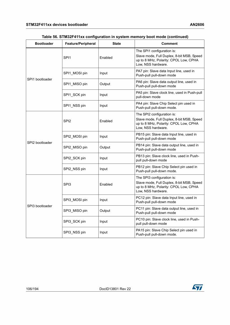
STM32F411xx devices bootloader AN2606
106/194 DocID13801 Rev 22
SPI1 bootloader
SPI1 Enabled
The SPI1 configuration is:
Slave mode, Full Duplex, 8-bit MSB, Speed up to 8 MHz, Polarity: CPOL Low, CPHA Low, NSS hardware.
SPI1_MOSI pin InputPA7 pin: Slave data Input line, used in Push-pull pull-down mode
SPI1_MISO pin OutputPA6 pin: Slave data output line, used in Push-pull pull-down mode
SPI1_SCK pin InputPA5 pin: Slave clock line, used in Push-pull pull-down mode
SPI1_NSS pin InputPA4 pin: Slave Chip Select pin used in Push-pull pull-down mode.
SPI2 bootloader
SPI2 Enabled
The SPI2 configuration is:
Slave mode, Full Duplex, 8-bit MSB, Speed up to 8 MHz, Polarity: CPOL Low, CPHA Low, NSS hardware.
SPI2_MOSI pin InputPB15 pin: Slave data Input line, used in Push-pull pull-down mode
SPI2_MISO pin OutputPB14 pin: Slave data output line, used in Push-pull pull-down mode
SPI2_SCK pin InputPB13 pin: Slave clock line, used in Push-pull pull-down mode
SPI2_NSS pin InputPB12 pin: Slave Chip Select pin used in Push-pull pull-down mode.
SPI3 bootloader
SPI3 Enabled
The SPI3 configuration is:
Slave mode, Full Duplex, 8-bit MSB, Speed up to 8 MHz, Polarity: CPOL Low, CPHA Low, NSS hardware.
SPI3_MOSI pin InputPC12 pin: Slave data Input line, used in Push-pull pull-down mode
SPI3_MISO pin OutputPC11 pin: Slave data output line, used in Push-pull pull-down mode
SPI3_SCK pin InputPC10 pin: Slave clock line, used in Push-pull pull-down mode
SPI3_NSS pin InputPA15 pin: Slave Chip Select pin used in Push-pull pull-down mode.
Table 56. STM32F411xx configuration in system memory boot mode (continued)
Bootloader Feature/Peripheral State Comment

DocID13801 Rev 22 107/194
AN2606 STM32F411xx devices bootloader
193
The system clock is derived from the embedded internal high-speed RC for USARTx, I2Cx and SPIx bootloaders. This internal clock is also used for CAN and DFU (USB FS Device) but only for the selection phase. An external clock multiple of 1 MHz (between 4 and 26 MHz) is required for CAN and DFU bootloader execution after the selection phase.
DFU bootloader
USB EnabledUSB OTG FS configured in Forced Device mode
USB_DM pin
Input/Output
PA11: USB DM line.
USB_DP pinPA12: USB DP line
No external Pull-up resistor is required
TIM11 Enabled
This timer is used to determine the value of the HSE. Once the HSE frequency is determined, the system clock is configured to 60 MHz using PLL and HSE.
Table 56. STM32F411xx configuration in system memory boot mode (continued)
Bootloader Feature/Peripheral State Comment

STM32F411xx devices bootloader AN2606
108/194 DocID13801 Rev 22
28.2 Bootloader selection
The figure below shows the bootloader selection mechanism.
Figure 31. Bootloader selection for STM32F411xx

DocID13801 Rev 22 109/194
AN2606 STM32F411xx devices bootloader
193
28.3 Bootloader version
The following table lists the STM32F411xx devices bootloader version.
Table 57. STM32F411xx bootloader versions
Bootloader version number Description Known limitations
V13.0 Initial bootloader version None

STM32F42xxx/43xxx devices bootloader AN2606
110/194 DocID13801 Rev 22
29 STM32F42xxx/43xxx devices bootloader
29.1 Bootloader V7.x
29.1.1 Bootloader configuration
The STM32F42xxx/43xxx bootloader is activated by applying pattern5 (described in Table 2: Bootloader activation patterns). The following table shows the hardware resources used by this bootloader.
Table 58. STM32F42xxx/43xxx configuration in system memory boot mode
Bootloader Feature/Peripheral State Comment
Common to all bootloaders
RCC
HSI enabled
The system clock frequency is 24 MHz using the PLL.
The HSI clock source is used at startup (interface detection phase) and when USART or I2C interfaces are selected (once CAN or DFU bootloader is selected, the clock source will be derived from the external crystal).
HSE enabled
The system clock frequency is 60 MHz.
The HSE clock source is used only when the CAN or the DFU (USB FS Device) interfaces are selected.
The external clock must provide a frequency multiple of 1 MHz and ranging from 4 MHz to 26 MHz.
-
The Clock Security System (CSS) interrupt is enabled for the CAN and DFU bootloaders. Any failure (or removal) of the external clock generates system reset.
RAM -8 Kbytes starting from address 0x20000000 are used by the bootloader firmware
System memory -30424 bytes starting from address 0x1FFF0000, contain the bootloader firmware
IWDG -
The independent watchdog (IWDG) prescaler is configured to its maximum value. It is periodically refreshed to prevent watchdog reset (in case the hardware IWDG option was previously enabled by the user).
Power -
Voltage range is set to [1.62 V, 2.1 V]. In this range internal Flash write operations are allowed only in byte format (Half-Word, Word and Double-Word operations are not allowed). The voltage range can be configured in run time using bootloader commands.
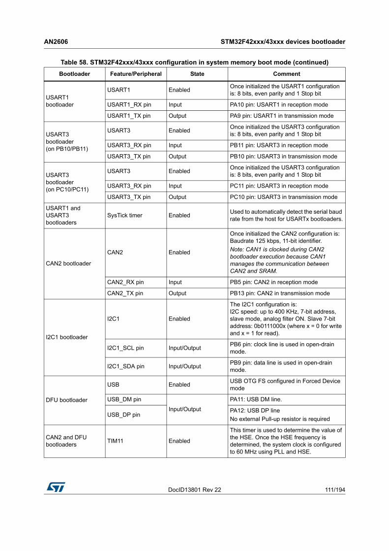
DocID13801 Rev 22 111/194
AN2606 STM32F42xxx/43xxx devices bootloader
193
USART1 bootloader
USART1 EnabledOnce initialized the USART1 configuration is: 8 bits, even parity and 1 Stop bit
USART1_RX pin Input PA10 pin: USART1 in reception mode
USART1_TX pin Output PA9 pin: USART1 in transmission mode
USART3 bootloader (on PB10/PB11)
USART3 EnabledOnce initialized the USART3 configuration is: 8 bits, even parity and 1 Stop bit
USART3_RX pin Input PB11 pin: USART3 in reception mode
USART3_TX pin Output PB10 pin: USART3 in transmission mode
USART3 bootloader (on PC10/PC11)
USART3 EnabledOnce initialized the USART3 configuration is: 8 bits, even parity and 1 Stop bit
USART3_RX pin Input PC11 pin: USART3 in reception mode
USART3_TX pin Output PC10 pin: USART3 in transmission mode
USART1 and USART3 bootloaders
SysTick timer EnabledUsed to automatically detect the serial baud rate from the host for USARTx bootloaders.
CAN2 bootloader
CAN2 Enabled
Once initialized the CAN2 configuration is: Baudrate 125 kbps, 11-bit identifier.
Note: CAN1 is clocked during CAN2 bootloader execution because CAN1 manages the communication between CAN2 and SRAM.
CAN2_RX pin Input PB5 pin: CAN2 in reception mode
CAN2_TX pin Output PB13 pin: CAN2 in transmission mode
I2C1 bootloader
I2C1 Enabled
The I2C1 configuration is: I2C speed: up to 400 KHz, 7-bit address, slave mode, analog filter ON. Slave 7-bit address: 0b0111000x (where x = 0 for write and x = 1 for read).
I2C1_SCL pin Input/OutputPB6 pin: clock line is used in open-drain mode.
I2C1_SDA pin Input/OutputPB9 pin: data line is used in open-drain mode.
DFU bootloader
USB EnabledUSB OTG FS configured in Forced Device mode
USB_DM pin
Input/Output
PA11: USB DM line.
USB_DP pinPA12: USB DP line
No external Pull-up resistor is required
CAN2 and DFU bootloaders
TIM11 Enabled
This timer is used to determine the value of the HSE. Once the HSE frequency is determined, the system clock is configured to 60 MHz using PLL and HSE.
Table 58. STM32F42xxx/43xxx configuration in system memory boot mode (continued)
Bootloader Feature/Peripheral State Comment

STM32F42xxx/43xxx devices bootloader AN2606
112/194 DocID13801 Rev 22
The system clock is derived from the embedded internal high-speed RC for USARTx and I2Cx bootloaders. This internal clock is also used for CAN and DFU (USB FS Device) but only for the selection phase. An external clock multiple of 1 MHz (between 4 and 26 MHz) is required for CAN and DFU bootloader execution after the selection phase.
29.1.2 Bootloader selection
The figures below show the bootloader selection mechanism.
Figure 32. Dual Bank Boot Implementation for STM32F42xxx/43xxx Bootloader V7.x

DocID13801 Rev 22 113/194
AN2606 STM32F42xxx/43xxx devices bootloader
193
Figure 33. Bootloader V7.x selection for STM32F42xxx/43xxx
STM32F42xxx/43xxx devices bootloader AN2606
114/194 DocID13801 Rev 22
29.1.3 Bootloader version
The following table lists the STM32F42xxx/43xxx devices bootloader V7.x versions.
Initial bootloader version
For the CAN interface, the Write Unprotect command is not functional. Instead you can use Write Memory command and write directly to the option bytes in order to disable the write protection.
29.2 Bootloader V9.x
29.2.1 Bootloader configuration
The STM32F42xxx/43xxx bootloader is activated by applying pattern5 (described in Table 2: Bootloader activation patterns). The following table shows the hardware resources used by this bootloader.
Table 59. STM32F42xxx/43xxx bootloader V7.x versions
Bootloader version number
Description Known limitations
V7.0

DocID13801 Rev 22 115/194
AN2606 STM32F42xxx/43xxx devices bootloader
193
Table 60. STM32F42xxx/43xxx configuration in system memory boot mode
Bootloader Feature/Peripheral State Comment
Common to all
bootloaders
RCC
HSI enabled
The system clock frequency is 60 MHz using the PLL.
The HSI clock source is used at startup (interface detection phase) and when USART or SPI or I2C interfaces are selected (once CAN or DFU bootloader is selected, the clock source will be derived from the external crystal).
HSE enabled
The system clock frequency is 60 MHz.
The HSE clock source is used only when the CAN or the DFU (USB FS Device) interfaces are selected.
The external clock must provide a frequency multiple of 1 MHz and ranging from 4 MHz to 26 MHz.
-
The Clock Security System (CSS) interrupt is enabled for the CAN and DFU bootloaders. Any failure (or removal) of the external clock generates system reset.
RAM -12 Kbytes starting from address 0x20000000 are used by the bootloader firmware
System memory -30424 bytes starting from address 0x1FFF0000, contain the bootloader firmware
IWDG -
The independent watchdog (IWDG) prescaler is configured to its maximum value. It is periodically refreshed to prevent watchdog reset (in case the hardware IWDG option was previously enabled by the user).
Power -
Voltage range is set to [1.62 V, 2.1 V]. In this range internal Flash write operations are allowed only in byte format (Half-Word, Word and Double-Word operations are not allowed). The voltage range can be configured in run time using bootloader commands.
USART1
bootloader
USART1 EnabledOnce initialized the USART1 configuration is: 8-bits, even parity and 1 Stop bit
USART1_RX pin Input PA10 pin: USART1 in reception mode
USART1_TX pin Output PA9 pin: USART1 in transmission mode
USART3
bootloader (on
PB10/PB11)
USART3 EnabledOnce initialized the USART3 configuration is: 8-bits, even parity and 1 Stop bit
USART3_RX pin Input PB11 pin: USART3 in reception mode
USART3_TX pin Output PB10 pin: USART3 in transmission mode
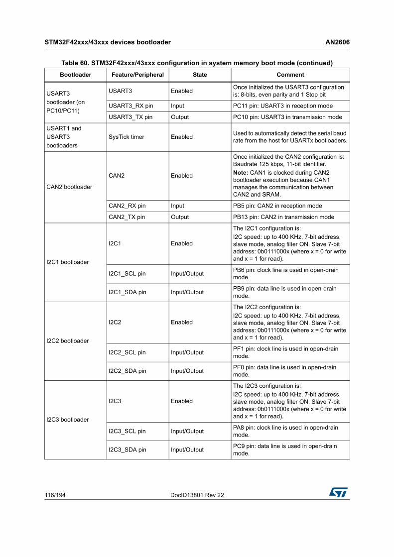
STM32F42xxx/43xxx devices bootloader AN2606
116/194 DocID13801 Rev 22
USART3
bootloader (on
PC10/PC11)
USART3 EnabledOnce initialized the USART3 configuration is: 8-bits, even parity and 1 Stop bit
USART3_RX pin Input PC11 pin: USART3 in reception mode
USART3_TX pin Output PC10 pin: USART3 in transmission mode
USART1 and
USART3
bootloaders
SysTick timer EnabledUsed to automatically detect the serial baud rate from the host for USARTx bootloaders.
CAN2 bootloader
CAN2 Enabled
Once initialized the CAN2 configuration is: Baudrate 125 kbps, 11-bit identifier.
Note: CAN1 is clocked during CAN2 bootloader execution because CAN1 manages the communication between CAN2 and SRAM.
CAN2_RX pin Input PB5 pin: CAN2 in reception mode
CAN2_TX pin Output PB13 pin: CAN2 in transmission mode
I2C1 bootloader
I2C1 Enabled
The I2C1 configuration is:
I2C speed: up to 400 KHz, 7-bit address, slave mode, analog filter ON. Slave 7-bit address: 0b0111000x (where x = 0 for write and x = 1 for read).
I2C1_SCL pin Input/OutputPB6 pin: clock line is used in open-drain mode.
I2C1_SDA pin Input/OutputPB9 pin: data line is used in open-drain mode.
I2C2 bootloader
I2C2 Enabled
The I2C2 configuration is:
I2C speed: up to 400 KHz, 7-bit address, slave mode, analog filter ON. Slave 7-bit address: 0b0111000x (where x = 0 for write and x = 1 for read).
I2C2_SCL pin Input/OutputPF1 pin: clock line is used in open-drain mode.
I2C2_SDA pin Input/OutputPF0 pin: data line is used in open-drain mode.
I2C3 bootloader
I2C3 Enabled
The I2C3 configuration is:
I2C speed: up to 400 KHz, 7-bit address, slave mode, analog filter ON. Slave 7-bit address: 0b0111000x (where x = 0 for write and x = 1 for read).
I2C3_SCL pin Input/OutputPA8 pin: clock line is used in open-drain mode.
I2C3_SDA pin Input/OutputPC9 pin: data line is used in open-drain mode.
Table 60. STM32F42xxx/43xxx configuration in system memory boot mode (continued)
Bootloader Feature/Peripheral State Comment

DocID13801 Rev 22 117/194
AN2606 STM32F42xxx/43xxx devices bootloader
193
SPI1 bootloader
SPI1 Enabled
The SPI1 configuration is:
Slave mode, Full Duplex, 8-bit MSB, Speed up to 8 MHz, Polarity: CPOL Low, CPHA Low, NSS hardware.
SPI1_MOSI pin InputPA7 pin: Slave data Input line, used in Push-pull pull-down mode
SPI1_MISO pin OutputPA6 pin: Slave data output line, used in Push-pull pull-down mode
SPI1_SCK pin InputPA5 pin: Slave clock line, used in Push-pull pull-down mode
SPI1_NSS pin InputPA4 pin: Slave Chip Select pin used in Push-pull pull-down mode.
SPI2 bootloader
SPI2 Enabled
The SPI2 configuration is:
Slave mode, Full Duplex, 8-bit MSB, Speed up to 8 MHz, Polarity: CPOL Low, CPHA Low, NSS hardware.
SPI2_MOSI pin InputPI3 pin: Slave data Input line, used in Push-pull pull-down mode
SPI2_MISO pin OutputPI2 pin: Slave data output line, used in Push-pull pull-down mode
SPI2_SCK pin InputPI1 pin: Slave clock line, used in Push-pull pull-down mode
SPI2_NSS pin InputPI0 pin: Slave Chip Select pin used in Push-pull pull-down mode.
SPI4 bootloader
SPI4 Enabled
The SPI4 configuration is:
Slave mode, Full Duplex, 8-bit MSB, Speed up to 8 MHz, Polarity: CPOL Low, CPHA Low, NSS hardware.
SPI4_MOSI pin InputPE14 pin: Slave data Input line, used in Push-pull pull-down mode
SPI4_MISO pin OutputPE13 pin: Slave data output line, used in Push-pull pull-down mode
SP4_SCK pin InputPE12 pin: Slave clock line, used in Push-pull pull-down mode
SPI4_NSS pin InputPE11 pin: Slave Chip Select pin used in Push-pull pull-down mode.
Table 60. STM32F42xxx/43xxx configuration in system memory boot mode (continued)
Bootloader Feature/Peripheral State Comment

STM32F42xxx/43xxx devices bootloader AN2606
118/194 DocID13801 Rev 22
The system clock is derived from the embedded internal high-speed RC for USARTx, I2Cx and SPIx bootloaders. This internal clock is also used for CAN and DFU (USB FS Device) but only for the selection phase. An external clock multiple of 1 MHz (between 4 and 26 MHz) is required for CAN and DFU bootloader execution after the selection phase.
DFU bootloader
USB EnabledUSB OTG FS configured in Forced Device mode
USB_DM pin
Input/Output
PA11: USB DM line.
USB_DP pinPA12: USB DP line
No external Pull-up resistor is required
CAN2 and DFU bootloaders
TIM11 Enabled
This timer is used to determine the value of the HSE. Once the HSE frequency is determined, the system clock is configured to 60 MHz using PLL and HSE.
Table 60. STM32F42xxx/43xxx configuration in system memory boot mode (continued)
Bootloader Feature/Peripheral State Comment
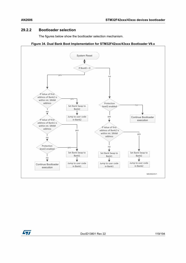
DocID13801 Rev 22 119/194
AN2606 STM32F42xxx/43xxx devices bootloader
193
29.2.2 Bootloader selection
The figures below show the bootloader selection mechanism.
Figure 34. Dual Bank Boot Implementation for STM32F42xxx/43xxx Bootloader V9.x
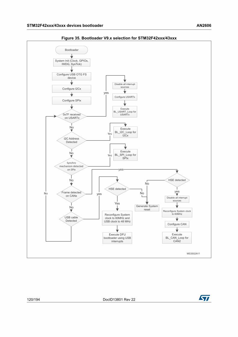
STM32F42xxx/43xxx devices bootloader AN2606
120/194 DocID13801 Rev 22
Figure 35. Bootloader V9.x selection for STM32F42xxx/43xxx
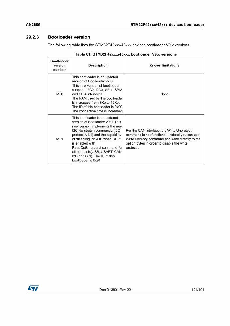
DocID13801 Rev 22 121/194
AN2606 STM32F42xxx/43xxx devices bootloader
193
29.2.3 Bootloader version
The following table lists the STM32F42xxx/43xxx devices bootloader V9.x versions.
Table 61. STM32F42xxx/43xxx bootloader V9.x versions
Bootloader version number
Description Known limitations
V9.0
This bootloader is an updated version of Bootloader v7.0. This new version of bootloader supports I2C2, I2C3, SPI1, SPI2 and SPI4 interfaces. The RAM used by this bootloader is increased from 8Kb to 12Kb. The ID of this bootloader is 0x90 The connection time is increased.
None
V9.1
This bootloader is an updated version of Bootloader v9.0. This new version implements the new I2C No-stretch commands (I2C protocol v1.1) and the capability of disabling PcROP when RDP1 is enabled with ReadOutUnprotect command for all protocols(USB, USART, CAN, I2C and SPI). The ID of this bootloader is 0x91
For the CAN interface, the Write Unprotect command is not functional. Instead you can use Write Memory command and write directly to the option bytes in order to disable the write protection.
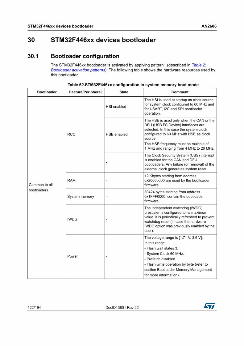
STM32F446xx devices bootloader AN2606
122/194 DocID13801 Rev 22
30 STM32F446xx devices bootloader
30.1 Bootloader configuration
The STM32F446xx bootloader is activated by applying pattern1 (described in Table 2: Bootloader activation patterns). The following table shows the hardware resources used by this bootloader.
Table 62.STM32F446xx configuration in system memory boot mode
Bootloader Feature/Peripheral State Comment
Common to all
bootloaders
RCC
HSI enabled
The HSI is used at startup as clock source for system clock configured to 60 MHz and for USART, I2C and SPI bootloader operation.
HSE enabled
The HSE is used only when the CAN or the DFU (USB FS Device) interfaces are selected. In this case the system clock configured to 60 MHz with HSE as clock source.
The HSE frequency must be multiple of 1 MHz and ranging from 4 MHz to 26 MHz.
-
The Clock Security System (CSS) interrupt is enabled for the CAN and DFU bootloaders. Any failure (or removal) of the external clock generates system reset.
RAM -12 Kbytes starting from address 0x20000000 are used by the bootloader firmware
System memory -30424 bytes starting from address 0x1FFF0000, contain the bootloader firmware
IWDG -
The independent watchdog (IWDG) prescaler is configured to its maximum value. It is periodically refreshed to prevent watchdog reset (in case the hardware IWDG option was previously enabled by the user).
Power -
The voltage range is [1.71 V, 3.6 V].
In this range:
- Flash wait states 3.
- System Clock 60 MHz.
- Prefetch disabled.
- Flash write operation by byte (refer to
section Bootloader Memory Management
for more information).

DocID13801 Rev 22 123/194
AN2606 STM32F446xx devices bootloader
193
USART1
bootloader
USART1 EnabledOnce initialized the USART1 configuration is: 8-bits, even parity and 1 Stop bit
USART1_RX pin Input PA10 pin: USART1 in reception mode
USART1_TX pin Output PA9 pin: USART1 in transmission mode
USART3
bootloader (on
PB10/PB11)
USART3 EnabledOnce initialized the USART3 configuration is: 8-bits, even parity and 1 Stop bit
USART3_RX pin Input PB11 pin: USART3 in reception mode
USART3_TX pin Output PB10 pin: USART3 in transmission mode
USART3
bootloader (on
PC10/PC11)
USART3 EnabledOnce initialized the USART3 configuration is: 8-bits, even parity and 1 Stop bit
USART3_RX pin Input PC11 pin: USART3 in reception mode
USART3_TX pin Output PC10 pin: USART3 in transmission mode
USART1 and
USART3
bootloaders
SysTick timer EnabledUsed to automatically detect the serial baud rate from the host for USARTx bootloaders.
CAN2 bootloader
CAN2 Enabled
Once initialized the CAN2 configuration is: Baudrate 125 kbps, 11-bit identifier.
Note: CAN1 is clocked during CAN2 bootloader execution because in CAN1 manages the communication between CAN2 and SRAM.
CAN2_RX pin Input PB5 pin: CAN2 in reception mode
CAN2_TX pin Output PB13 pin: CAN2 in transmission mode
I2C1 bootloader
I2C1 Enabled
The I2C1 configuration is:
I2C speed: up to 400 KHz, 7-bit address, slave mode, analog filter ON.
Slave 7-bit address: 0b0111100x
(where x = 0 for write and x = 1 for read)
I2C1_SCL pin Input/OutputPB6 pin: clock line is used in open-drain mode.
I2C1_SDA pin Input/OutputPB9 pin: data line is used in open-drain mode.
I2C2 bootloader
I2C2 Enabled
The I2C2 configuration is:
I2C speed: up to 400 KHz, 7-bit address, slave mode, analog filter ON.
Slave 7-bit address: 0b0111100x
(where x = 0 for write and x = 1 for read)
I2C2_SCL pin Input/OutputPF1 pin: clock line is used in open-drain mode.
I2C2_SDA pin Input/OutputPF0 pin: data line is used in open-drain mode.
Table 62.STM32F446xx configuration in system memory boot mode (continued)
Bootloader Feature/Peripheral State Comment

STM32F446xx devices bootloader AN2606
124/194 DocID13801 Rev 22
I2C3 bootloader
I2C3 Enabled
The I2C3 configuration is:
I2C speed: up to 400 KHz, 7-bit address, slave mode, analog filter ON.
Slave 7-bit address: 0b0111100x
(where x = 0 for write and x = 1 for read)
I2C3_SCL pin Input/OutputPA8 pin: clock line is used in open-drain mode.
I2C3_SDA pin Input/OutputPC9 pin: data line is used in open-drain mode.
SPI1 bootloader
SPI1 Enabled
The SPI1 configuration is:
Slave mode, Full Duplex, 8-bit MSB, Speed up to 8 MHz, Polarity: CPOL Low, CPHA Low, NSS hardware.
SPI1_MOSI pin InputPA7 pin: Slave data Input line, used in Push-pull pull-down mode
SPI1_MISO pin OutputPA6 pin: Slave data output line, used in Push-pull pull-down mode
SPI1_SCK pin InputPA5 pin: Slave clock line, used in Push-pull pull-down mode
SPI1_NSS pin InputPA4 pin: Slave Chip Select pin used in Push-pull pull-up mode.
SPI2 bootloader
SPI2 Enabled
The SPI2 configuration is:
Slave mode, Full Duplex, 8-bit MSB, Speed up to 8 MHz, Polarity: CPOL Low, CPHA Low, NSS hardware.
SPI2_MOSI pin InputPB15 pin: Slave data Input line, used in Push-pull pull-down mode
SPI2_MISO pin OutputPB14 pin: Slave data output line, used in Push-pull pull-down mode
SPI2_SCK pin InputPC7 pin: Slave clock line, used in Push-pull pull-down mode
SPI2_NSS pin InputPB12 pin: Slave Chip Select pin used in Push-pull pull-up mode.
Table 62.STM32F446xx configuration in system memory boot mode (continued)
Bootloader Feature/Peripheral State Comment

DocID13801 Rev 22 125/194
AN2606 STM32F446xx devices bootloader
193
The system clock is derived from the embedded internal high-speed RC for USARTx and I2Cx bootloaders. This internal clock is also used for CAN and DFU (USB FS Device) but only for the selection phase. An external clock multiple of 1 MHz (between 4 and 26 MHz) is required for CAN and DFU bootloader execution after the selection phase.
SPI4 bootloader
SPI4 Enabled
The SPI4 configuration is:
Slave mode, Full Duplex, 8-bit MSB, Speed up to 8 MHz, Polarity: CPOL Low, CPHA Low, NSS hardware.
SPI4_MOSI pin InputPE14 pin: Slave data Input line, used in Push-pull pull-down mode
SPI4_MISO pin OutputPE13 pin: Slave data output line, used in Push-pull pull-down mode
SPI4_SCK pin InputPE12 pin: Slave clock line, used in Push-pull pull-down mode
SPI4_NSS pin InputPE11 pin: Slave Chip Select pin used in Push-pull pull-up mode.
DFU bootloader
USB EnabledUSB OTG FS configured in Forced Device mode
USB_DM pin
Input/Output
PA11: USB DM line.
USB_DP pinPA12: USB DP line
No external Pull-up resistor is required
CAN2 and DFU bootloaders
TIM17 Enabled
This timer is used to determine the value of the HSE. Once the HSE frequency is determinated, the system clock is configured to 60 MHz using PLL and HSE.
Table 62.STM32F446xx configuration in system memory boot mode (continued)
Bootloader Feature/Peripheral State Comment
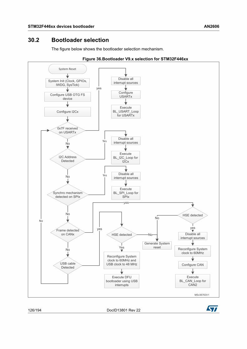
STM32F446xx devices bootloader AN2606
126/194 DocID13801 Rev 22
30.2 Bootloader selection
The figure below shows the bootloader selection mechanism.
Figure 36.Bootloader V9.x selection for STM32F446xx

DocID13801 Rev 22 127/194
AN2606 STM32F446xx devices bootloader
193
30.3 Bootloader version
The following table lists the STM32F446xx devices bootloader V9.x versions:
Table 63. STM32F446xx bootloader V9.x versions
Bootloader version number
Description Known limitations
V9.0 Initial bootloader version None

STM32F74xxx/75xxx devices bootloader AN2606
128/194 DocID13801 Rev 22
31 STM32F74xxx/75xxx devices bootloader
Two bootloader versions are available on STM32F74xxx/75xxx:
• V7.x supporting USART1, USART3, CAN2, I2C1, I2C2, I2C3 and DFU (USB FS Device). This version is embedded in STM32F74xxx/75xxx rev. A devices.
• V9.x supporting USART1, USART3, CAN2, I2C1, I2C2, I2C3, SPI1, SPI2, SPI4 and DFU (USB FS Device). This version is embedded in STM32F74xxx/75xxx rev. Z devices.
31.1 Bootloader V7.x
31.1.1 Bootloader configuration
The STM32F74xxx/75xxx bootloader is activated by applying pattern8 (described in Table 2: Bootloader activation patterns). The following table shows the hardware resources used by this bootloader.
Table 64. STM32F74xxx/75xxx configuration in system memory boot mode
Bootloader Feature/Peripheral State Comment
Common to all
bootloaders
RCC
HSI enabledThe HSI is used at startup as clock source for system clock configured to 60 MHz and for USART and I2C bootloader operation.
HSE enabled
The HSE is used only when the CAN or the DFU (USB FS Device) interfaces are selected. In this case the system clock configured to 60 MHz with HSE as clock source.
The HSE frequency must be multiple of 1 MHz and ranging from 4 MHz to 26 MHz.
-
The Clock Security System (CSS) interrupt
is enabled for the CAN and DFU
bootloaders. Any failure (or removal) of the
external clock generates system reset.
RAM -16 Kbytes starting from address 0x20000000 are used by the bootloader firmware
System memory -61440 bytes starting from address 0x1FF00000, contain the bootloader firmware
IWDG -
The independent watchdog (IWDG) prescaler is configured to its maximum value. It is periodically refreshed to prevent watchdog reset (in case the hardware IWDG option was previously enabled by the user).
Power -
The voltage range is [1.8V, 3.6V]. In this range:
- Flash wait states 3.
- System clock Frequency 60 MHz.
- ART Accelerator enabled.
- Flash write operation by byte (refer to Bootloader Memory Management section for more information).
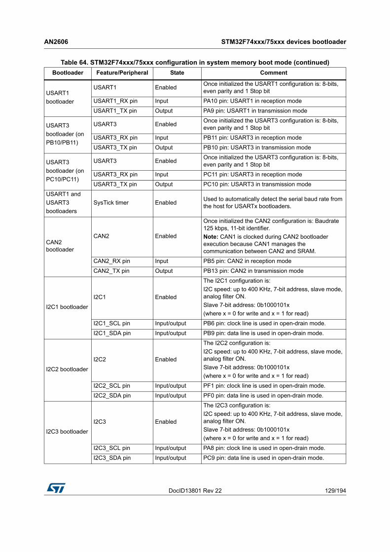
DocID13801 Rev 22 129/194
AN2606 STM32F74xxx/75xxx devices bootloader
193
USART1
bootloader
USART1 EnabledOnce initialized the USART1 configuration is: 8-bits, even parity and 1 Stop bit
USART1_RX pin Input PA10 pin: USART1 in reception mode
USART1_TX pin Output PA9 pin: USART1 in transmission mode
USART3
bootloader (on
PB10/PB11)
USART3 EnabledOnce initialized the USART3 configuration is: 8-bits, even parity and 1 Stop bit
USART3_RX pin Input PB11 pin: USART3 in reception mode
USART3_TX pin Output PB10 pin: USART3 in transmission mode
USART3
bootloader (on
PC10/PC11)
USART3 EnabledOnce initialized the USART3 configuration is: 8-bits, even parity and 1 Stop bit
USART3_RX pin Input PC11 pin: USART3 in reception mode
USART3_TX pin Output PC10 pin: USART3 in transmission mode
USART1 and
USART3
bootloaders
SysTick timer EnabledUsed to automatically detect the serial baud rate from the host for USARTx bootloaders.
CAN2 bootloader
CAN2 Enabled
Once initialized the CAN2 configuration is: Baudrate 125 kbps, 11-bit identifier.
Note: CAN1 is clocked during CAN2 bootloader execution because CAN1 manages the communication between CAN2 and SRAM.
CAN2_RX pin Input PB5 pin: CAN2 in reception mode
CAN2_TX pin Output PB13 pin: CAN2 in transmission mode
I2C1 bootloader
I2C1 Enabled
The I2C1 configuration is:
I2C speed: up to 400 KHz, 7-bit address, slave mode, analog filter ON.
Slave 7-bit address: 0b1000101x
(where x = 0 for write and x = 1 for read)
I2C1_SCL pin Input/output PB6 pin: clock line is used in open-drain mode.
I2C1_SDA pin Input/output PB9 pin: data line is used in open-drain mode.
I2C2 bootloader
I2C2 Enabled
The I2C2 configuration is:
I2C speed: up to 400 KHz, 7-bit address, slave mode, analog filter ON.
Slave 7-bit address: 0b1000101x
(where x = 0 for write and x = 1 for read)
I2C2_SCL pin Input/output PF1 pin: clock line is used in open-drain mode.
I2C2_SDA pin Input/output PF0 pin: data line is used in open-drain mode.
I2C3 bootloader
I2C3 Enabled
The I2C3 configuration is:
I2C speed: up to 400 KHz, 7-bit address, slave mode, analog filter ON.
Slave 7-bit address: 0b1000101x
(where x = 0 for write and x = 1 for read)
I2C3_SCL pin Input/output PA8 pin: clock line is used in open-drain mode.
I2C3_SDA pin Input/output PC9 pin: data line is used in open-drain mode.
Table 64. STM32F74xxx/75xxx configuration in system memory boot mode (continued)
Bootloader Feature/Peripheral State Comment

STM32F74xxx/75xxx devices bootloader AN2606
130/194 DocID13801 Rev 22
The system clock is derived from the embedded internal high-speed RC for USARTx and I2Cx bootloaders. This internal clock is also used for CAN and DFU (USB FS Device) but only for the selection phase. An external clock multiple of 1 MHz (between 4 and 26 MHz) is required for CAN and DFU bootloader execution after the selection phase.
DFU bootloader
USB Enabled USB OTG FS configured in Forced Device mode.
USB_DM pin
Input/Output
PA11 pin: USB DM line.
USB_DP pinPA12 pin: USB DP line
No external Pull-Up resistor is required.
CAN2 and DFU bootloaders
TIM11 EnabledThis timer is used to determine the value of the HSE. Once HSE frequency is determined, the system clock is configured to 60 MHz using PLL and HSE.
Table 64. STM32F74xxx/75xxx configuration in system memory boot mode (continued)
Bootloader Feature/Peripheral State Comment

DocID13801 Rev 22 131/194
AN2606 STM32F74xxx/75xxx devices bootloader
193
31.1.2 Bootloader selection
The figure below shows the bootloader selection mechanism.
Figure 37.Bootloader V7.x selection for STM32F74xxx/75xxx

STM32F74xxx/75xxx devices bootloader AN2606
132/194 DocID13801 Rev 22
31.1.3 Bootloader version
The following table lists the STM32F74xxx/75xxx devices bootloader V7.x versions:
Table 65.STM32F74xxx/75xxx bootloader V7.x versions
Bootloader version number
Description Known limitations
V7.0 Initial bootloader version None

DocID13801 Rev 22 133/194
AN2606 STM32F74xxx/75xxx devices bootloader
193
31.2 Bootloader V9.x
31.2.1 Bootloader configuration
The STM32F74xxx/75xxx bootloader is activated by applying pattern8 (described in Table 2: Bootloader activation patterns). The following table shows the hardware resources used by this bootloader.
Table 66. STM32F74xxx/75xxx configuration in system memory boot mode
Bootloader Feature/Peripheral State Comment
Common to all
bootloaders
RCC
HSI enabled
The HSI is used at startup as clock source for system clock configured to 60MHz and for USART, I2C and SPI bootloader operation.
HSE enabled
The HSE is used only when the CAN or the DFU (USB FS Device) interfaces are selected. In this case the system clock configured to 60 MHz with HSE as clock source.
The HSE frequency must be multiple of 1 MHz and ranging from 4 MHz to 26 MHz.
-
The Clock Security System (CSS) interrupt
is enabled for the CAN and DFU
bootloaders. Any failure (or removal) of the
external clock generates system reset.
RAM -16 Kbytes starting from address 0x20000000 are used by the bootloader firmware
System memory -61440 bytes starting from address 0x1FF00000, contain the bootloader firmware
IWDG -
The independent watchdog (IWDG) prescaler is configured to its maximum value. It is periodically refreshed to prevent watchdog reset (in case the hardware IWDG option was previously enabled by the user).
Power -
The voltage range is [1.8V, 3.6V]
In this range:
- Flash wait states 3.
- System clock Frequency 60MHz.
- ART Accelerator enabled.
- Flash write operation by byte (refer to Bootloader Memory Management section for more information).

STM32F74xxx/75xxx devices bootloader AN2606
134/194 DocID13801 Rev 22
USART1
bootloader
USART1 EnabledOnce initialized the USART1 configuration is: 8-bits, even parity and 1 Stop bit
USART1_RX pin Input PA10 pin: USART1 in reception mode
USART1_TX pin Output PA9 pin: USART1 in transmission mode
USART3
bootloader (on
PB10/PB11)
USART3 EnabledOnce initialized the USART3 configuration is: 8-bits, even parity and 1 Stop bit
USART3_RX pin Input PB11 pin: USART3 in reception mode
USART3_TX pin Output PB10 pin: USART3 in transmission mode
USART3
bootloader (on
PC10/PC11)
USART3 EnabledOnce initialized the USART3 configuration is: 8-bits, even parity and 1 Stop bit
USART3_RX pin Input PC11 pin: USART3 in reception mode
USART3_TX pin Output PC10 pin: USART3 in transmission mode
USART1 and
USART3
bootloaders
SysTick timer EnabledUsed to automatically detect the serial baud rate from the host for USARTx bootloaders.
CAN2 bootloader
CAN2 Enabled
Once initialized the CAN2 configuration is: Baudrate 125 kbps, 11-bit identifier.
Note: CAN1 is clocked during CAN2 bootloader execution because CAN1 manages the communication between CAN2 and SRAM.
CAN2_RX pin Input PB5 pin: CAN2 in reception mode
CAN2_TX pin Output PB13 pin: CAN2 in transmission mode
I2C1 bootloader
I2C1 Enabled
The I2C1 configuration is:
I2C speed: up to 400 KHz, 7-bit address, slave mode, analog filter ON.
Slave 7-bit address: 0b1000101x
(where x = 0 for write and x = 1 for read)
I2C1_SCL pin Input/outputPB6 pin: clock line is used in open-drain mode.
I2C1_SDA pin Input/outputPB9 pin: data line is used in open-drain mode.
I2C2 bootloader
I2C2 Enabled
The I2C2 configuration is:
I2C speed: up to 400 KHz, 7-bit address, slave mode, analog filter ON.
Slave 7-bit address: 0b1000101x
(where x = 0 for write and x = 1 for read)
I2C2_SCL pin Input/outputPF1 pin: clock line is used in open-drain mode.
I2C2_SDA pin Input/outputPF0 pin: data line is used in open-drain mode.
Table 66. STM32F74xxx/75xxx configuration in system memory boot mode (continued)
Bootloader Feature/Peripheral State Comment

DocID13801 Rev 22 135/194
AN2606 STM32F74xxx/75xxx devices bootloader
193
I2C3 bootloader
I2C3 Enabled
The I2C3 configuration is:
I2C speed: up to 400 KHz, 7-bit address, slave mode, analog filter ON.
Slave 7-bit address: 0b1000101x
(where x = 0 for write and x = 1 for read)
I2C3_SCL pin Input/outputPA8 pin: clock line is used in open-drain mode.
I2C3_SDA pin Input/outputPC9 pin: data line is used in open-drain mode.
SPI1 bootloader
SPI1 Enabled
The SPI1 configuration is:
Slave mode, Full Duplex, 8-bit MSB, Speed up to 8 MHz, Polarity: CPOL Low, CPHA Low, NSS hardware.
SPI1_MOSI pin InputPA7 pin: Slave data Input line, used in Push-pull pull-down mode
SPI1_MISO pin OutputPA6 pin: Slave data output line, used in Push-pull pull-down mode
SPI1_SCK pin InputPA5 pin: Slave clock line, used in Push-pull pull-down mode
SPI1_NSS pin InputPA4 pin: Slave Chip Select pin used in Push-pull pull-up mode.
SPI2 bootloader
SPI2 Enabled
The SPI2 configuration is:
Slave mode, Full Duplex, 8-bit MSB, Speed up to 8 MHz, Polarity: CPOL Low, CPHA Low, NSS hardware.
SPI2_MOSI pin InputPI3 pin: Slave data Input line, used in Push-pull pull-down mode
SPI2_MISO pin OutputPI2 pin: Slave data output line, used in Push-pull pull-down mode
SPI2_SCK pin InputPI1 pin: Slave clock line, used in Push-pull pull-down mode
SPI2_NSS pin InputPI0 pin: Slave Chip Select pin used in Push-pull pull-up mode.
Table 66. STM32F74xxx/75xxx configuration in system memory boot mode (continued)
Bootloader Feature/Peripheral State Comment

STM32F74xxx/75xxx devices bootloader AN2606
136/194 DocID13801 Rev 22
The system clock is derived from the embedded internal high-speed RC for USARTx, I2Cx and SPIx bootloaders. This internal clock is also used for CAN and DFU (USB FS Device) but only for the selection phase. An external clock multiple of 1 MHz (between 4 and 26 MHz) is required for CAN and DFU bootloader execution after the selection phase.
31.2.2 Bootloader selection
The figure below shows the bootloader selection mechanism.
SPI4 bootloader
SPI4 Enabled
The SPI4 configuration is:
Slave mode, Full Duplex, 8-bit MSB, Speed up to 8 MHz, Polarity: CPOL Low, CPHA Low, NSS hardware.
SPI4_MOSI pin InputPE14 pin: Slave data Input line, used in Push-pull pull-down mode
SPI4_MISO pin OutputPE13 pin: Slave data output line, used in Push-pull pull-down mode
SP4_SCK pin InputPE12 pin: Slave clock line, used in Push-pull pull-down mode
SPI4_NSS pin InputPE11 pin: Slave Chip Select pin used in Push-pull pull-up mode.
DFU bootloader
USB EnabledUSB OTG FS configured in Forced Device mode.
USB_DM pin
Input/Output
PA11 pin: USB DM line.
USB_DP pinPA12 pin: USB DP line
No external Pull-Up resistor is required.
CAN2 and DFU bootloaders
TIM11 Enabled
This timer is used to determine the value of the HSE. Once HSE frequency is determined, the system clock is configured to 60 MHz using PLL and HSE.
Table 66. STM32F74xxx/75xxx configuration in system memory boot mode (continued)
Bootloader Feature/Peripheral State Comment

DocID13801 Rev 22 137/194
AN2606 STM32F74xxx/75xxx devices bootloader
193
Figure 38.Bootloader V9.x selection for STM32F74xxx/75xxx

STM32F74xxx/75xxx devices bootloader AN2606
138/194 DocID13801 Rev 22
31.2.3 Bootloader version
The following table lists the STM32F74xxx/75xxx bootloader V9.x versions:
Table 67.STM32F74xxx/75xxx bootloader V9.x versions
Bootloader version number
Description Known limitations
V9.0 Initial bootloader version None
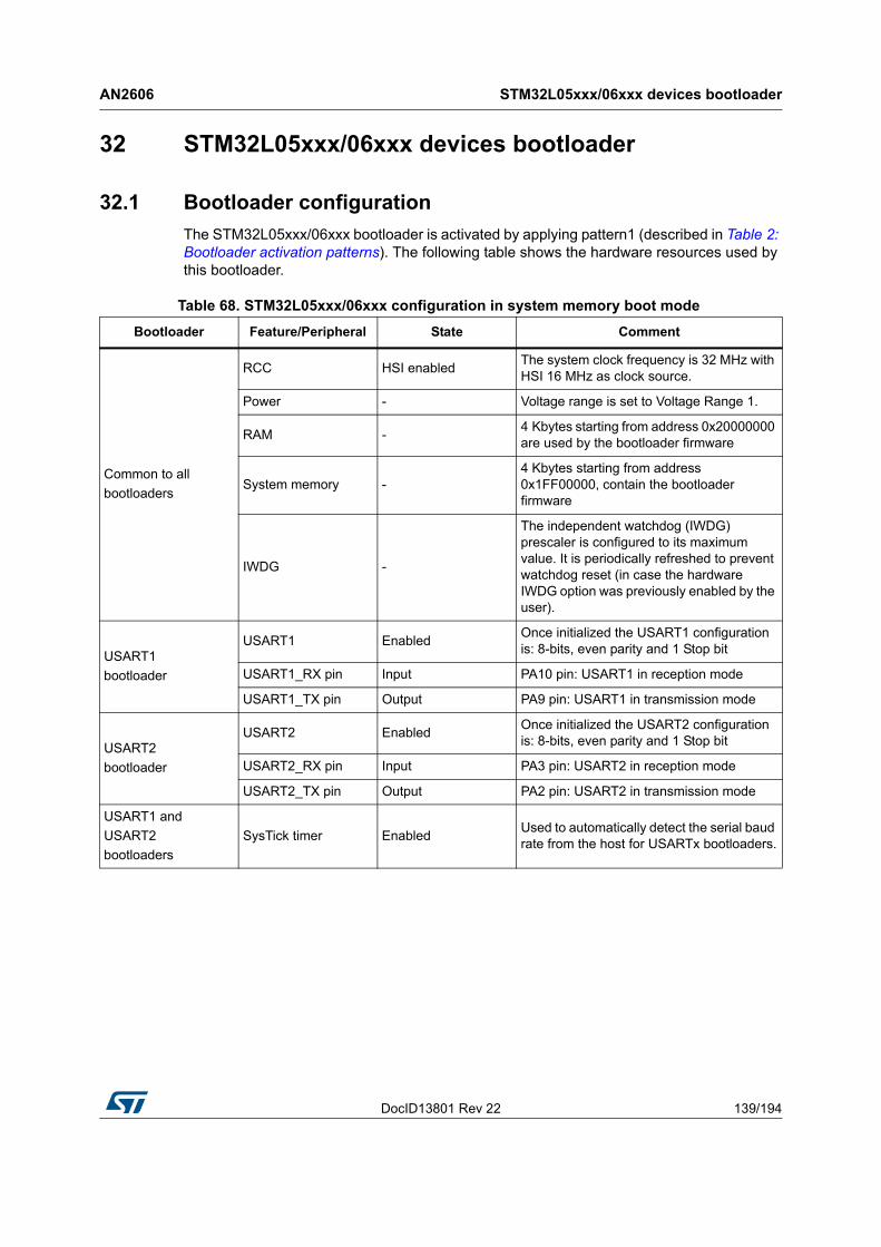
DocID13801 Rev 22 139/194
AN2606 STM32L05xxx/06xxx devices bootloader
193
32 STM32L05xxx/06xxx devices bootloader
32.1 Bootloader configuration
The STM32L05xxx/06xxx bootloader is activated by applying pattern1 (described in Table 2: Bootloader activation patterns). The following table shows the hardware resources used by this bootloader.
Table 68. STM32L05xxx/06xxx configuration in system memory boot mode
Bootloader Feature/Peripheral State Comment
Common to all
bootloaders
RCC HSI enabledThe system clock frequency is 32 MHz with HSI 16 MHz as clock source.
Power - Voltage range is set to Voltage Range 1.
RAM -4 Kbytes starting from address 0x20000000 are used by the bootloader firmware
System memory -4 Kbytes starting from address 0x1FF00000, contain the bootloader firmware
IWDG -
The independent watchdog (IWDG) prescaler is configured to its maximum value. It is periodically refreshed to prevent watchdog reset (in case the hardware IWDG option was previously enabled by the user).
USART1
bootloader
USART1 EnabledOnce initialized the USART1 configuration is: 8-bits, even parity and 1 Stop bit
USART1_RX pin Input PA10 pin: USART1 in reception mode
USART1_TX pin Output PA9 pin: USART1 in transmission mode
USART2
bootloader
USART2 EnabledOnce initialized the USART2 configuration is: 8-bits, even parity and 1 Stop bit
USART2_RX pin Input PA3 pin: USART2 in reception mode
USART2_TX pin Output PA2 pin: USART2 in transmission mode
USART1 and
USART2
bootloaders
SysTick timer EnabledUsed to automatically detect the serial baud rate from the host for USARTx bootloaders.
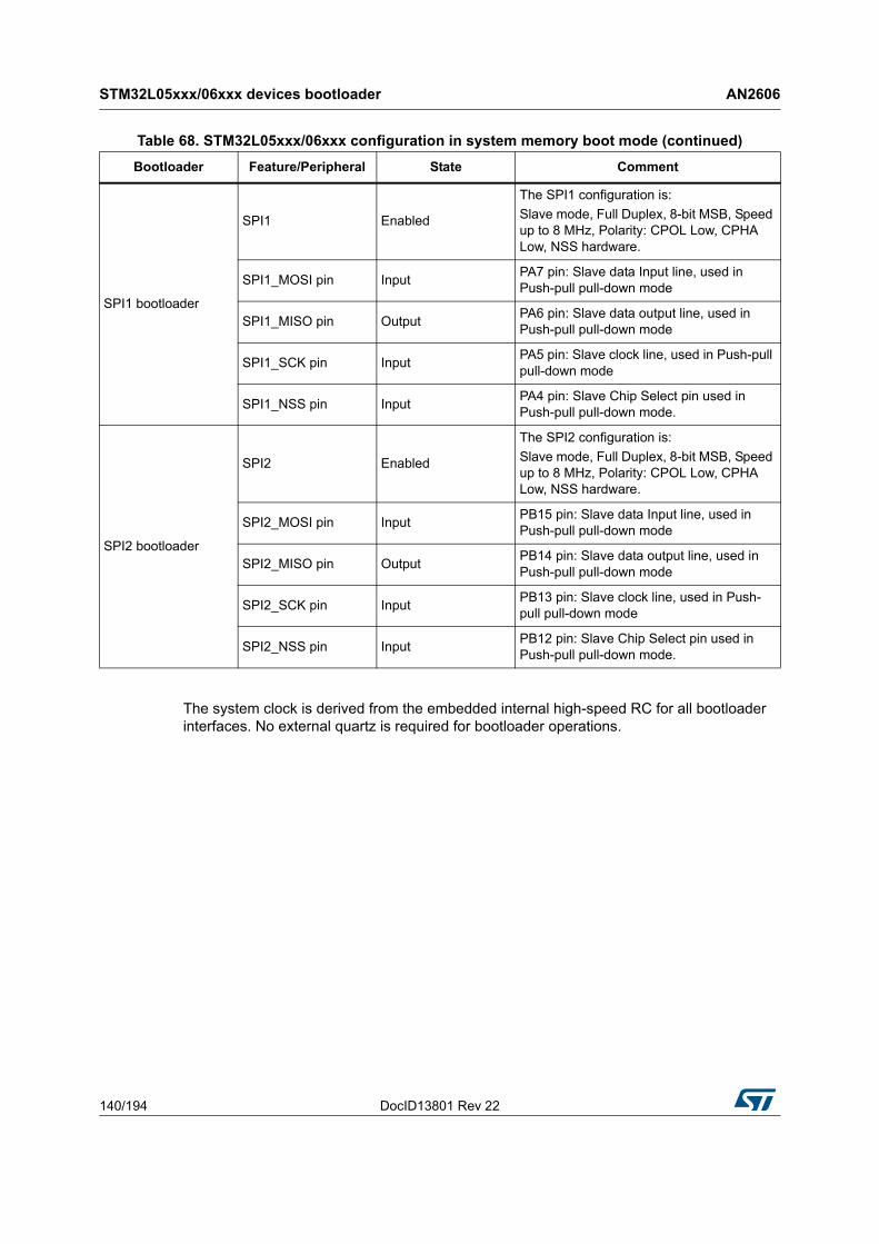
STM32L05xxx/06xxx devices bootloader AN2606
140/194 DocID13801 Rev 22
The system clock is derived from the embedded internal high-speed RC for all bootloader interfaces. No external quartz is required for bootloader operations.
SPI1 bootloader
SPI1 Enabled
The SPI1 configuration is:
Slave mode, Full Duplex, 8-bit MSB, Speed up to 8 MHz, Polarity: CPOL Low, CPHA Low, NSS hardware.
SPI1_MOSI pin InputPA7 pin: Slave data Input line, used in Push-pull pull-down mode
SPI1_MISO pin OutputPA6 pin: Slave data output line, used in Push-pull pull-down mode
SPI1_SCK pin InputPA5 pin: Slave clock line, used in Push-pull pull-down mode
SPI1_NSS pin InputPA4 pin: Slave Chip Select pin used in Push-pull pull-down mode.
SPI2 bootloader
SPI2 Enabled
The SPI2 configuration is:
Slave mode, Full Duplex, 8-bit MSB, Speed up to 8 MHz, Polarity: CPOL Low, CPHA Low, NSS hardware.
SPI2_MOSI pin InputPB15 pin: Slave data Input line, used in Push-pull pull-down mode
SPI2_MISO pin OutputPB14 pin: Slave data output line, used in Push-pull pull-down mode
SPI2_SCK pin InputPB13 pin: Slave clock line, used in Push-pull pull-down mode
SPI2_NSS pin InputPB12 pin: Slave Chip Select pin used in Push-pull pull-down mode.
Table 68. STM32L05xxx/06xxx configuration in system memory boot mode (continued)
Bootloader Feature/Peripheral State Comment
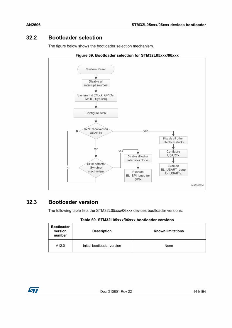
DocID13801 Rev 22 141/194
AN2606 STM32L05xxx/06xxx devices bootloader
193
32.2 Bootloader selection
The figure below shows the bootloader selection mechanism.
Figure 39. Bootloader selection for STM32L05xxx/06xxx
32.3 Bootloader version
The following table lists the STM32L05xxx/06xxx devices bootloader versions:
Table 69. STM32L05xxx/06xxx bootloader versions
Bootloader version number
Description Known limitations
V12.0 Initial bootloader version None

STM32L1xxx6(8/B)A devices bootloader AN2606
142/194 DocID13801 Rev 22
33 STM32L1xxx6(8/B)A devices bootloader
33.1 Bootloader configuration
The STM32L1xxx6(8/B)A bootloader is activated by applying pattern1 (described in Table 2: Bootloader activation patterns). The following table shows the hardware resources used by this bootloader.
The system clock is derived from the embedded internal high-speed RC, no external quartz is required for the bootloader execution.
Table 70. STM32L1xxx6(8/B)A configuration in system memory boot mode
Bootloader Feature/Peripheral State Comment
Common to all
bootloaders
RCC HSI enabled The system clock frequency is 16 MHz.
RAM -2 Kbytes starting from address 0x20000000 are used by the bootloader firmware.
System memory -4 Kbytes starting from address 0x1FF00000 contain the bootloader firmware.
IWDG -
The independent watchdog (IWDG) prescaler is configured to its maximum value and is periodically refreshed to prevent watchdog reset (in case the hardware IWDG option was previously enabled by the user).
Power - Voltage range is set to Voltage Range 1.
USART1
bootloader
USART1 EnabledOnce initialized, the USART1 configuration is: 8 bits, even parity and 1 Stop bit.
USART1_RX pin Input PA10 pin: USART1 in reception mode
USART1_TX pin Output PA9 pin: USART1 in transmission mode
USART2
bootloader
USART2 EnabledOnce initialized, the USART2 configuration is: 8 bits, even parity and 1 Stop bit.
USART2_RX pin Input PD6 pin: USART2 in reception mode
USART2_TX pin Output PD5 pin: USART2 in transmission mode
USART1 and
USART2
bootloaders
SysTick timer EnabledUsed to automatically detect the serial baud rate from the host.

DocID13801 Rev 22 143/194
AN2606 STM32L1xxx6(8/B)A devices bootloader
193
33.2 Bootloader selection
The figure below shows the bootloader selection mechanism.
Figure 40. Bootloader selection for STM32L1xxx6(8/B)A devices
33.3 Bootloader version
The following table lists the STM32L1xxx6(8/B)A devices bootloader versions:
Table 71. STM32L1xxx6(8/B)A bootloader versions
Bootloader version number
Description Known limitations
V2.0 Initial bootloader version
When a Read Memory command or Write Memory command is issued with an unsupported memory address and a correct address checksum (ie. address 0x6000 0000), the command is aborted by the bootloader device, but the NACK (0x1F) is not sent to the host. As a result, the next 2 bytes (which are the number of bytes to be read/written and its checksum) are considered as a new command and its checksum.(1)
1. If the “number of data - 1” (N-1) to be read/written is not equal to a valid command code, then the limitation is not perceived from the host since the command is NACKed anyway (as an unsupported new command).

STM32L1xxx6(8/B) devices bootloader AN2606
144/194 DocID13801 Rev 22
34 STM32L1xxx6(8/B) devices bootloader
34.1 Bootloader configuration
The STM32L1xxx6(8/B) bootloader is activated by applying pattern1 (described in Table 2: Bootloader activation patterns). The following table shows the hardware resources used by this bootloader.
The system clock is derived from the embedded internal high-speed RC, no external quartz is required for the bootloader execution.
Table 72. STM32L1xxx6(8/B) configuration in system memory boot mode
Bootloader Feature/Peripheral State Comment
Common to all
bootloaders
RCC HSI enabled The system clock frequency is 16 MHz.
RAM -2 Kbytes starting from address 0x20000000 are used by the bootloader firmware.
System memory -4 Kbytes starting from address 0x1FF00000 contain the bootloader firmware.
IWDG -
The independent watchdog (IWDG) prescaler is configured to its maximum value and is periodically refreshed to prevent watchdog reset (in case the hardware IWDG option was previously enabled by the user).
Power - Voltage range is set to Voltage Range 1.
USART1
bootloader
USART1 EnabledOnce initialized, the USART1 configuration is: 8 bits, even parity and 1 Stop bit.
USART1_RX pin Input PA10 pin: USART1 in reception mode
USART1_TX pin Output PA9 pin: USART1 in transmission mode
USART2
bootloader
USART2 EnabledOnce initialized, the USART2 configuration is: 8 bits, even parity and 1 Stop bit.
USART2_RX pin Input PD6 pin: USART2 in reception mode
USART2_TX pin Output PD5 pin: USART2 in transmission mode
USART1 and
USART2
bootloaders
SysTick timer EnabledUsed to automatically detect the serial baud rate from the host.
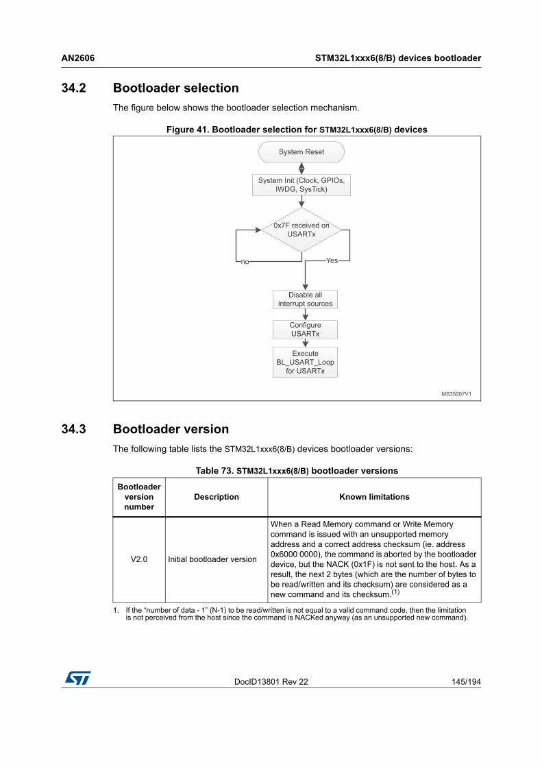
DocID13801 Rev 22 145/194
AN2606 STM32L1xxx6(8/B) devices bootloader
193
34.2 Bootloader selection
The figure below shows the bootloader selection mechanism.
Figure 41. Bootloader selection for STM32L1xxx6(8/B) devices
34.3 Bootloader version
The following table lists the STM32L1xxx6(8/B) devices bootloader versions:
Table 73. STM32L1xxx6(8/B) bootloader versions
Bootloader version number
Description Known limitations
V2.0 Initial bootloader version
When a Read Memory command or Write Memory command is issued with an unsupported memory address and a correct address checksum (ie. address 0x6000 0000), the command is aborted by the bootloader device, but the NACK (0x1F) is not sent to the host. As a result, the next 2 bytes (which are the number of bytes to be read/written and its checksum) are considered as a new command and its checksum.(1)
1. If the “number of data - 1” (N-1) to be read/written is not equal to a valid command code, then the limitation is not perceived from the host since the command is NACKed anyway (as an unsupported new command).

STM32L1xxxC devices bootloader AN2606
146/194 DocID13801 Rev 22
35 STM32L1xxxC devices bootloader
35.1 Bootloader configuration
The STM32L1xxxC bootloader is activated by applying pattern1 (described in Table 2: Bootloader activation patterns). The following table shows the hardware resources used by this bootloader.
Table 74. STM32L1xxxC configuration in system memory boot mode
Bootloader Feature/Peripheral State Comment
Common to all bootloaders
RCC
HSI enabled
The system clock frequency is 16 MHz using the HSI. This is used only for USART1 and USART2 bootloaders and during USB detection for DFU bootloader (once the DFU bootloader is selected, the clock source is derived from the external crystal).
HSE enabled
The external clock is mandatory only for the DFU bootloader and must be in the following range: [24, 16, 12, 8, 6, 4, 3, 2] MHz.
The PLL is used to generate the USB 48 MHz clock and the 32 MHz clock for the system clock.
-
The Clock Security System (CSS) interrupt is enabled for the DFU bootloader. Any failure (or removal) of the external clock generates a system reset.
IWDG -
The independent watchdog (IWDG) prescaler is configured to its maximum value and is periodically refreshed to prevent watchdog resets (in case the hardware IWDG option was previously enabled by the user).
Power - Voltage range is set to Voltage Range 1.
System memory -8 Kbytes starting from address 0x1FF0 0000. This area contains the bootloader firmware.
RAM -4 Kbytes starting from address 0x20000000 are used by the bootloader firmware.
USART1 bootloader
USART1 EnabledOnce initialized, the USART1 configuration is 8 bits, even parity and 1 stop bit.
USART1_RX pin Input PA10 pin: USART1 in reception mode
USART1_TX pin Output PA9 pin: USART1 in transmission mode
USART1 and USART2 bootloaders
SysTick timer EnabledUsed to automatically detect the serial baud rate from the host for the USARTx bootloader.
DocID13801 Rev 22 147/194
AN2606 STM32L1xxxC devices bootloader
193
The system clock is derived from the embedded internal high-speed RC for the USARTx bootloader. This internal clock is also used the for DFU bootloader but only for the selection phase. An external clock in the range of [24, 16, 12, 8, 6, 4, 3, 2] MHz is required for the execution of the DFU bootloader after the selection phase.
USART2 bootloader
USART2 EnabledOnce initialized, the USART2 configuration is 8 bits, even parity and 1 stop bit. The USART2 uses its remapped pins.
USART2_RX pin Input PD6 pin: USART2 in reception mode
USART2_TX pin Output PD5 pin: USART2 in transmission mode
DFU bootloader
USB Enabled USB used in FS mode
USB_DM pin
Input/Output
PA11: USB DM line.
USB_DP pinPA12: USB DP line
An external pull-up resistor 1.5 KOhm must be connected to USB_DP pin.
Table 74. STM32L1xxxC configuration in system memory boot mode (continued)
Bootloader Feature/Peripheral State Comment
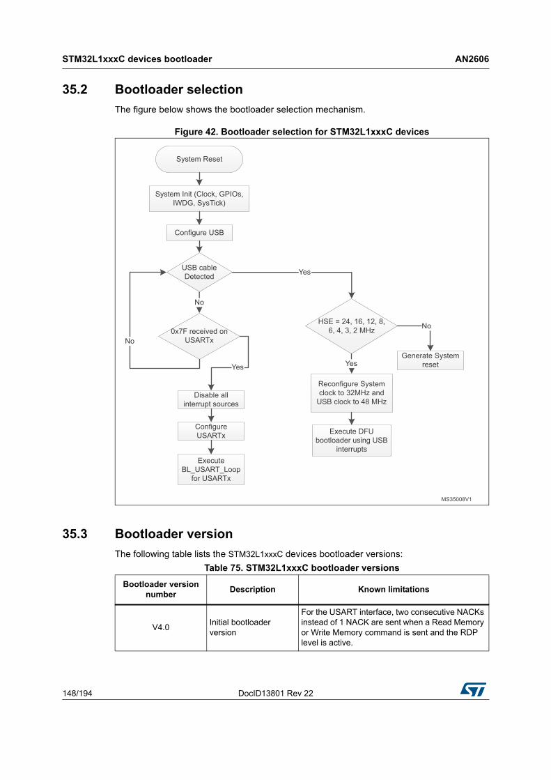
STM32L1xxxC devices bootloader AN2606
148/194 DocID13801 Rev 22
35.2 Bootloader selection
The figure below shows the bootloader selection mechanism.
Figure 42. Bootloader selection for STM32L1xxxC devices
35.3 Bootloader version
The following table lists the STM32L1xxxC devices bootloader versions:
Initial bootloader version
For the USART interface, two consecutive NACKs instead of 1 NACK are sent when a Read Memory or Write Memory command is sent and the RDP level is active.
Table 75. STM32L1xxxC bootloader versions
Bootloader version number
Description Known limitations
V4.0

DocID13801 Rev 22 149/194
AN2606 STM32L1xxxD devices bootloader
193
36 STM32L1xxxD devices bootloader
36.1 Bootloader configuration
The STM32L1xxxD bootloader is activated by applying pattern4 (described in Table 2: Bootloader activation patterns). The following table shows the hardware resources used by this bootloader.
Table 76. STM32L1xxxD configuration in system memory boot mode
Bootloader Feature/Peripheral State Comment
Common to all bootloaders
RCC
HSI enabled
The system clock frequency is 16 MHz using the HSI. This is used only for USART1 and USART2 bootloaders and during USB detection for DFU bootloader (once the DFU bootloader is selected, the clock source will be derived from the external crystal).
HSE enabled
The external clock is mandatory only for DFU bootloader and it must be in the following range: [24, 16, 12, 8, 6, 4, 3, 2] MHz.
The PLL is used to generate the USB 48 MHz clock and the 32 MHz clock for the system clock.
-
The Clock Security System (CSS) interrupt is enabled for the DFU bootloader. Any failure (or removal) of the external clock generates system reset.
IWDG -
The independent watchdog (IWDG) prescaler is configured to its maximum value and is periodically refreshed to prevent watchdog reset (in case the hardware IWDG option was previously enabled by the user).
Power - Voltage range is set to Voltage Range 1.
System memory -8 Kbytes starting from address 0x1FF0 0000. This area contains the bootloader firmware.
RAM -4 Kbytes starting from address 0x20000000 are used by the bootloader firmware.
USART1 bootloader
USART1 EnabledOnce initialized, the USART1 configuration is: 8 bits, even parity and 1 Stop bit.
USART1_RX pin Input PA10 pin: USART1 in reception mode
USART1_TX pin Output PA9 pin: USART1 in transmission mode
USART1 and USART2 bootloaders
SysTick timer EnabledUsed to automatically detect the serial baud rate from the host for USARTx bootloader.

STM32L1xxxD devices bootloader AN2606
150/194 DocID13801 Rev 22
The system clock is derived from the embedded internal high-speed RC for USARTx bootloader. This internal clock is used also for DFU bootloader but only for the selection phase. An external clock in the range of [24, 16, 12, 8, 6, 4, 3, 2] MHz is required for DFU bootloader execution after the selection phase.
USART2 bootloader
USART2 EnabledOnce initialized, the USART2 configuration is: 8 bits, even parity and 1 Stop bit. The USART2 uses its remapped pins.
USART2_RX pin Input PD6 pin: USART2 in reception mode
USART2_TX pin Output PD5 pin: USART2 in transmission mode
DFU bootloader
USB Enabled USB used in FS mode
USB_DM pin
Input/Output
PA11: USB DM line.
USB_DP pinPA12: USB DP line
An external pull-up resistor 1.5 KOhm must be connected to USB_DP pin.
Table 76. STM32L1xxxD configuration in system memory boot mode (continued)
Bootloader Feature/Peripheral State Comment

DocID13801 Rev 22 151/194
AN2606 STM32L1xxxD devices bootloader
193
36.2 Bootloader selection
The figure below shows the bootloader selection mechanism.
Figure 43. Bootloader selection for STM32L1xxxD devices

STM32L1xxxD devices bootloader AN2606
152/194 DocID13801 Rev 22
36.3 Bootloader version
The following table lists the STM32L1xxxD devices bootloader versions:
Table 77. STM32L1xxxD bootloader versions
Bootloader version number
Description Known limitations
V4.1 Initial bootloader version
– In the bootloader code the PA13 (JTMS/SWDIO) I/O output speed is configured to 400 KHz, as consequence some debugger can not connect to the device in Serial Wire mode when the bootloader is running.
– When the DFU bootloader is selected, the RTC is reset and thus all RTC information (calendar, alarm, ...) will be lost including backup registers. Note: When the USART bootloader is selected there is no change on the RTC configuration (including backup registers).
V4.2Fix V4.1 limitations (available on Rev.Z devices only.)
– Stack overflow by 8 bytes when jumping to Bank1/Bank2 if BFB2=0 or when Read Protection level is set to 2. Workaround: the user code should force in the startup file the top of stack address before to jump to the main program. This can be done in the “Reset_Handler” routine.
– When the Stack of the user code is placed outside the SRAM (ie. @ 0x2000C000) the bootloader cannot jump to that user code which is considered invalid. This might happen when using compilers which place the stack at a non-physical address at the top of the SRAM (ie. @ 0x2000C000). Workaround: place manually the stack at a physical address.
V4.5
Fix V4.2 limitations.
DFU interface robustness enhancements (available on Rev.Y devices only).
– For the USART interface, two consecutive NACKs (instead of 1 NACK) are sent when a Read Memory or Write Memory command is sent and the RDP level is active.
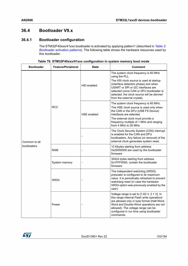
DocID13801 Rev 22 153/194
AN2606 STM32L1xxxD devices bootloader
193
36.4 Bootloader V9.x
36.4.1 Bootloader configuration
The STM32F40xxx/41xxx bootloader is activated by applying pattern1 (described in Table 2: Bootloader activation patterns). The following table shows the hardware resources used by this bootloader.
Table 78. STM32F40xxx/41xxx configuration in system memory boot mode
Bootloader Feature/Peripheral State Comment
Common to all
bootloaders
RCC
HSI enabled
The system clock frequency is 60 MHz using the PLL.
The HSI clock source is used at startup (interface detection phase) and when USART or SPI or I2C interfaces are selected (once CAN or DFU bootloader is selected, the clock source will be derived from the external crystal).
HSE enabled
The system clock frequency is 60 MHz.
The HSE clock source is used only when the CAN or the DFU (USB FS Device) interfaces are selected.
The external clock must provide a frequency multiple of 1 MHz and ranging from 4 MHz to 26 MHz.
-
The Clock Security System (CSS) interrupt is enabled for the CAN and DFU bootloaders. Any failure (or removal) of the external clock generates system reset.
RAM -12 Kbytes starting from address 0x20000000 are used by the bootloader firmware
System memory -30424 bytes starting from address 0x1FFF0000, contain the bootloader firmware
IWDG -
The independent watchdog (IWDG) prescaler is configured to its maximum value. It is periodically refreshed to prevent watchdog reset (in case the hardware IWDG option was previously enabled by the user).
Power -
Voltage range is set to [1.62 V, 2.1 V]. In this range internal Flash write operations are allowed only in byte format (Half-Word, Word and Double-Word operations are not allowed). The voltage range can be configured in run time using bootloader commands.
STM32L1xxxD devices bootloader AN2606
154/194 DocID13801 Rev 22
USART1
bootloader
USART1 EnabledOnce initialized the USART1 configuration is: 8-bits, even parity and 1 Stop bit
USART1_RX pin Input PA10 pin: USART1 in reception mode
USART1_TX pin Output PA9 pin: USART1 in transmission mode
USART3
bootloader (on
PB10/PB11)
USART3 EnabledOnce initialized the USART3 configuration is: 8-bits, even parity and 1 Stop bit
USART3_RX pin Input PB11 pin: USART3 in reception mode
USART3_TX pin Output PB10 pin: USART3 in transmission mode
USART3
bootloader (on
PC10/PC11)
USART3 EnabledOnce initialized the USART3 configuration is: 8-bits, even parity and 1 Stop bit
USART3_RX pin Input PC11 pin: USART3 in reception mode
USART3_TX pin Output PC10 pin: USART3 in transmission mode
USART1 and
USART3
bootloaders
SysTick timer EnabledUsed to automatically detect the serial baud rate from the host for USARTx bootloaders.
CAN2 bootloader
CAN2 Enabled
Once initialized the CAN2 configuration is: Baudrate 125 kbps, 11-bit identifier.
Note: CAN1 is clocked during CAN2 bootloader execution because CAN1 manages the communication between CAN2 and SRAM.
CAN2_RX pin Input PB5 pin: CAN2 in reception mode
CAN2_TX pin Output PB13 pin: CAN2 in transmission mode
I2C1 bootloader
I2C1 Enabled
The I2C1 configuration is:
I2C speed: up to 400 KHz, 7-bit address, slave mode, analog filter ON. Slave 7-bit address: 0b0111010x (where x = 0 for write and x = 1 for read).
I2C1_SCL pin Input/OutputPB6 pin: clock line is used in open-drain mode.
I2C1_SDA pin Input/OutputPB7 pin: data line is used in open-drain mode.
I2C2 bootloader
I2C2 Enabled
The I2C2 configuration is:
I2C speed: up to 400 KHz, 7-bit address, slave mode, analog filter ON. Slave 7-bit address: 0b0111010x (where x = 0 for write and x = 1 for read).
I2C2_SCL pin Input/OutputPF1 pin: clock line is used in open-drain mode.
I2C2_SDA pin Input/OutputPF0 pin: data line is used in open-drain mode.
Table 78. STM32F40xxx/41xxx configuration in system memory boot mode (continued)
Bootloader Feature/Peripheral State Comment
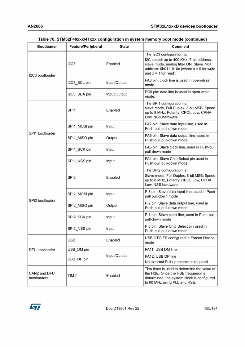
DocID13801 Rev 22 155/194
AN2606 STM32L1xxxD devices bootloader
193
I2C3 bootloader
I2C3 Enabled
The I2C3 configuration is:
I2C speed: up to 400 KHz, 7-bit address, slave mode, analog filter ON. Slave 7-bit address: 0b0111010x (where x = 0 for write and x = 1 for read).
I2C3_SCL pin Input/OutputPA8 pin: clock line is used in open-drain mode.
I2C3_SDA pin Input/OutputPC9 pin: data line is used in open-drain mode.
SPI1 bootloader
SPI1 Enabled
The SPI1 configuration is: slave mode, Full Duplex, 8-bit MSB, Speed up to 8 MHz, Polarity: CPOL Low, CPHA Low, NSS hardware.
SPI1_MOSI pin InputPA7 pin: Slave data Input line, used in Push-pull pull-down mode
SPI1_MISO pin OutputPA6 pin: Slave data output line, used in Push-pull pull-down mode
SPI1_SCK pin InputPA5 pin: Slave clock line, used in Push-pull pull-down mode
SPI1_NSS pin InputPA4 pin: Slave Chip Select pin used in Push-pull pull-down mode.
SPI2 bootloader
SPI2 Enabled
The SPI2 configuration is:
Slave mode, Full Duplex, 8-bit MSB, Speed up to 8 MHz, Polarity: CPOL Low, CPHA Low, NSS hardware.
SPI2_MOSI pin InputPI3 pin: Slave data Input line, used in Push-pull pull-down mode
SPI2_MISO pin OutputPI2 pin: Slave data output line, used in Push-pull pull-down mode
SPI2_SCK pin InputPI1 pin: Slave clock line, used in Push-pull pull-down mode
SPI2_NSS pin InputPI0 pin: Slave Chip Select pin used in Push-pull pull-down mode.
DFU bootloader
USB EnabledUSB OTG FS configured in Forced Device mode
USB_DM pin
Input/Output
PA11: USB DM line.
USB_DP pinPA12: USB DP line
No external Pull-up resistor is required
CAN2 and DFU bootloaders
TIM11 Enabled
This timer is used to determine the value of the HSE. Once the HSE frequency is determined, the system clock is configured to 60 MHz using PLL and HSE.
Table 78. STM32F40xxx/41xxx configuration in system memory boot mode (continued)
Bootloader Feature/Peripheral State Comment

STM32L1xxxD devices bootloader AN2606
156/194 DocID13801 Rev 22
The system clock is derived from the embedded internal high-speed RC for USARTx, I2Cx and SPIx bootloaders. This internal clock is also used for CAN and DFU (USB FS Device) but only for the selection phase. An external clock multiple of 1 MHz (between 4 and 26 MHz) is required for CAN and DFU bootloader execution after the selection phase.
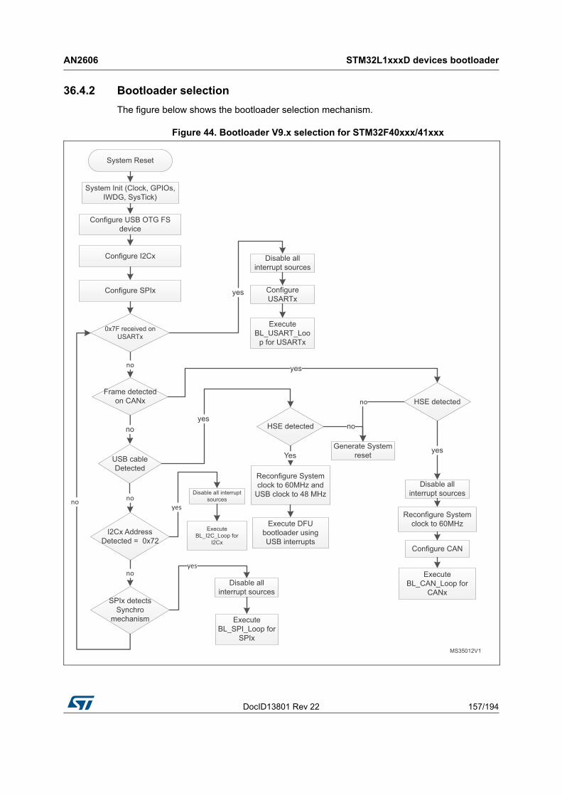
DocID13801 Rev 22 157/194
AN2606 STM32L1xxxD devices bootloader
193
36.4.2 Bootloader selection
The figure below shows the bootloader selection mechanism.
Figure 44. Bootloader V9.x selection for STM32F40xxx/41xxx
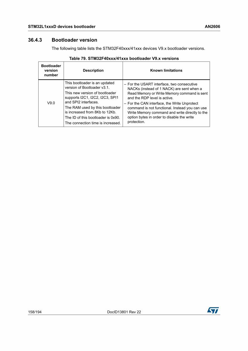
STM32L1xxxD devices bootloader AN2606
158/194 DocID13801 Rev 22
36.4.3 Bootloader version
The following table lists the STM32F40xxx/41xxx devices V9.x bootloader versions.
Table 79. STM32F40xxx/41xxx bootloader V9.x versions
Bootloader version number
Description Known limitations
V9.0
This bootloader is an updated version of Bootloader v3.1.
This new version of bootloader supports I2C1, I2C2, I2C3, SPI1 and SPI2 interfaces.
The RAM used by this bootloader is increased from 8Kb to 12Kb.
The ID of this bootloader is 0x90.
The connection time is increased.
– For the USART interface, two consecutive NACKs (instead of 1 NACK) are sent when a Read Memory or Write Memory command is sent and the RDP level is active.
– For the CAN interface, the Write Unprotect command is not functional. Instead you can use Write Memory command and write directly to the option bytes in order to disable the write protection.

DocID13801 Rev 22 159/194
AN2606 STM32L1xxxE devices bootloader
193
37 STM32L1xxxE devices bootloader
37.1 Bootloader configuration
The STM32L1xxxE bootloader is activated by applying pattern4 (described in Table 2: Bootloader activation patterns). The following table shows the hardware resources used by this bootloader.
Table 80. STM32L1xxxE configuration in system memory boot mode
Bootloader Feature/Peripheral State Comment
Common to all bootloaders
RCC
HSI enabled
The system clock frequency is 16 MHz using the HSI. This is used only for USART1 and USART2 bootloaders and during USB detection for DFU bootloader (once the DFU bootloader is selected, the clock source will be derived from the external crystal).
HSE enabled
The external clock is mandatory only for DFU bootloader and it must be in the following range: [24, 16, 12, 8, 6, 4, 3, 2] MHz.
The PLL is used to generate the USB 48 MHz clock and the 32 MHz clock for the system clock.
-
The Clock Security System (CSS) interrupt is enabled for the DFU bootloader. Any failure (or removal) of the external clock generates system reset.
IWDG -
The independent watchdog (IWDG) prescaler is configured to its maximum value and is periodically refreshed to prevent watchdog reset (in case the hardware IWDG option was previously enabled by the user).
Power - Voltage range is set to Voltage Range 1.
System memory -8 Kbytes starting from address 0x1FF0 0000. This area contains the bootloader firmware.
RAM -4 Kbytes starting from address 0x20000000 are used by the bootloader firmware.
USART1 bootloader
USART1 EnabledOnce initialized, the USART1 configuration is: 8 bits, even parity and 1 Stop bit.
USART1_RX pin Input PA10 pin: USART1 in reception mode
USART1_TX pin Output PA9 pin: USART1 in transmission mode
USART1 and USART2 bootloaders
SysTick timer EnabledUsed to automatically detect the serial baud rate from the host for USARTx bootloader.

STM32L1xxxE devices bootloader AN2606
160/194 DocID13801 Rev 22
The system clock is derived from the embedded internal high-speed RC for USARTx bootloader. This internal clock is used also for DFU bootloader but only for the selection phase. An external clock in the range of [24, 16, 12, 8, 6, 4, 3, 2] MHz is required for DFU bootloader execution after the selection phase.
USART2 bootloader
USART2 EnabledOnce initialized, the USART2 configuration is: 8 bits, even parity and 1 Stop bit. The USART2 uses its remapped pins.
USART2_RX pin Input PD6 pin: USART2 in reception mode
USART2_TX pin Output PD5 pin: USART2 in transmission mode
DFU bootloader
USB Enabled USB used in FS mode
USB_DM pin
Input/Output
PA11: USB DM line.
USB_DP pinPA12: USB DP line
An external pull-up resistor 1.5 KOhm must be connected to USB_DP pin.
Table 80. STM32L1xxxE configuration in system memory boot mode (continued)
Bootloader Feature/Peripheral State Comment

DocID13801 Rev 22 161/194
AN2606 STM32L1xxxE devices bootloader
193
37.2 Bootloader selection
The figure below shows the bootloader selection mechanism.
Figure 45. Bootloader selection for STM32L1xxxE devices

STM32L1xxxE devices bootloader AN2606
162/194 DocID13801 Rev 22
37.3 Bootloader version
The following table lists the STM32L1xxxE devices bootloader versions:
Table 81. STM32L1xxxE bootloader versions
Bootloader version number
Description Known limitations
V4.0 Initial bootloader version
– For the USART interface, two consecutive NACKs (instead of 1 NACK) are sent when a Read Memory or Write Memory command is sent and the RDP level is active.

DocID13801 Rev 22 163/194
AN2606 STM32L476xx/486xx devices bootloader
193
38 STM32L476xx/486xx devices bootloader
Two bootloader versions are available on STM32L476xx/486xx:
• V10.x supporting USART1, USART2,I2C1, I2C2 and DFU (USB FS Device). This version is embedded in STM32L476xx/486xx rev. A, rev. Z and rev. B devices.
• V9.x supporting USART1, USART2, I2C1, I2C2, SPI1 and SPI2, CAN1 and DFU (USB FS Device). This version is embedded in STM32L476xx/486xx rev. Y devices.
38.1 Bootloader V10.x
38.1.1 Bootloader configuration
The STM32L476xx/486xx bootloader is activated by applying pattern7 (described in Table 2: Bootloader activation patterns). The following table shows the hardware resources used by this bootloader.
Table 82. STM32L476xx/486xx configuration in system memory boot mode
Bootloader Feature/Peripheral State Comment
Common to all bootloaders
RCC
HSI enabledThe HSI is used at startup as clock source for system clock configured to 72 MHz and for USART and I2C bootloader operation.
HSE enabledThe HSE is used only when the USB interface is selected and the LSE is not present. The HSE must have one of the following value [24,20,18,16,12,9,8,6,4] MHz.
LSE enabled
The LSE is used to trim the MSI which is configured to 48 MHz as USB clock source. The LSE must be equal to 32,768 KHz. If the LSE is not detected, the HSE will be used instead if USB is connected.
MSI enabledThe MSI is configured to 48 MHz and will be used as USB clock source. The MSI is used only if LSE is detected, otherwise, HSE will be used if USB is connected.
-The Clock Security System (CSS) interrupt is enabled when LSE or HSE is enabled. Any failure (or removal) of the external clock generates system reset.
RAM -12 Kbytes starting from address 0x20000000 are used by the bootloader firmware
System memory -28672 bytes starting from address 0x1FFF0000, contain the bootloader firmware
IWDG -
The independent watchdog (IWDG) prescaler is configured to its maximum value. It is periodically refreshed to prevent watchdog reset (in case the hardware IWDG option was previously enabled by the user).
Power -
The DFU can’t be used to communicate with Bootloader if the voltage scaling range 2 is selected. Bootloader firmware doesn’t configure voltage scaling range value in PWR_CR1 register.
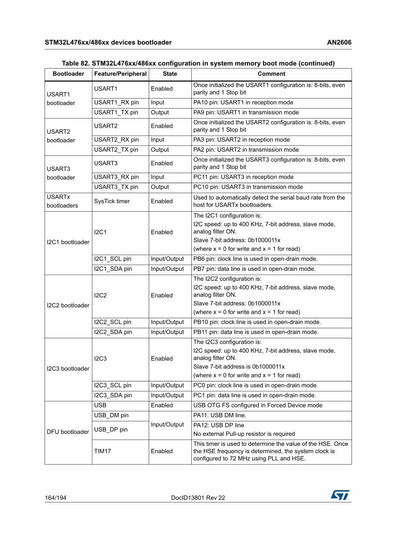
STM32L476xx/486xx devices bootloader AN2606
164/194 DocID13801 Rev 22
USART1
bootloader
USART1 EnabledOnce initialized the USART1 configuration is: 8-bits, even parity and 1 Stop bit
USART1_RX pin Input PA10 pin: USART1 in reception mode
USART1_TX pin Output PA9 pin: USART1 in transmission mode
USART2
bootloader
USART2 EnabledOnce initialized the USART2 configuration is: 8-bits, even parity and 1 Stop bit
USART2_RX pin Input PA3 pin: USART2 in reception mode
USART2_TX pin Output PA2 pin: USART2 in transmission mode
USART3
bootloader
USART3 EnabledOnce initialized the USART3 configuration is: 8-bits, even parity and 1 Stop bit
USART3_RX pin Input PC11 pin: USART3 in reception mode
USART3_TX pin Output PC10 pin: USART3 in transmission mode
USARTx
bootloadersSysTick timer Enabled
Used to automatically detect the serial baud rate from the host for USARTx bootloaders.
I2C1 bootloader
I2C1 Enabled
The I2C1 configuration is:
I2C speed: up to 400 KHz, 7-bit address, slave mode, analog filter ON.
Slave 7-bit address: 0b1000011x
(where x = 0 for write and x = 1 for read)
I2C1_SCL pin Input/Output PB6 pin: clock line is used in open-drain mode.
I2C1_SDA pin Input/Output PB7 pin: data line is used in open-drain mode.
I2C2 bootloader
I2C2 Enabled
The I2C2 configuration is:
I2C speed: up to 400 KHz, 7-bit address, slave mode, analog filter ON.
Slave 7-bit address: 0b1000011x
(where x = 0 for write and x = 1 for read)
I2C2_SCL pin Input/Output PB10 pin: clock line is used in open-drain mode.
I2C2_SDA pin Input/Output PB11 pin: data line is used in open-drain mode.
I2C3 bootloader
I2C3 Enabled
The I2C3 configuration is:
I2C speed: up to 400 KHz, 7-bit address, slave mode, analog filter ON.
Slave 7-bit address is 0b1000011x
(where x = 0 for write and x = 1 for read)
I2C3_SCL pin Input/Output PC0 pin: clock line is used in open-drain mode.
I2C3_SDA pin Input/Output PC1 pin: data line is used in open-drain mode.
DFU bootloader
USB Enabled USB OTG FS configured in Forced Device mode
USB_DM pin
Input/Output
PA11: USB DM line.
USB_DP pinPA12: USB DP line
No external Pull-up resistor is required
TIM17 EnabledThis timer is used to determine the value of the HSE. Once the HSE frequency is determined, the system clock is configured to 72 MHz using PLL and HSE.
Table 82. STM32L476xx/486xx configuration in system memory boot mode (continued)
Bootloader Feature/Peripheral State Comment
DocID13801 Rev 22 165/194
AN2606 STM32L476xx/486xx devices bootloader
193
For USARTx and I2Cx bootloaders no external clock is required.
USB bootloader (DFU) requires either an LSE (low-speed external clock) or a HSE (high-speed external clock) :
• In case, the LSE is present regardless the HSE presence, the MSI will be configured and trimmed by the LSE to provide an accurate clock equal to 48 MHz which is the clock source of the USB. The system clock is kept clocked to 24 MHz by the HSI.
• In case, the HSE is present, the system clock and USB clock will be configured respectively to 24 MHz and 48 MHz with HSE as clock source.
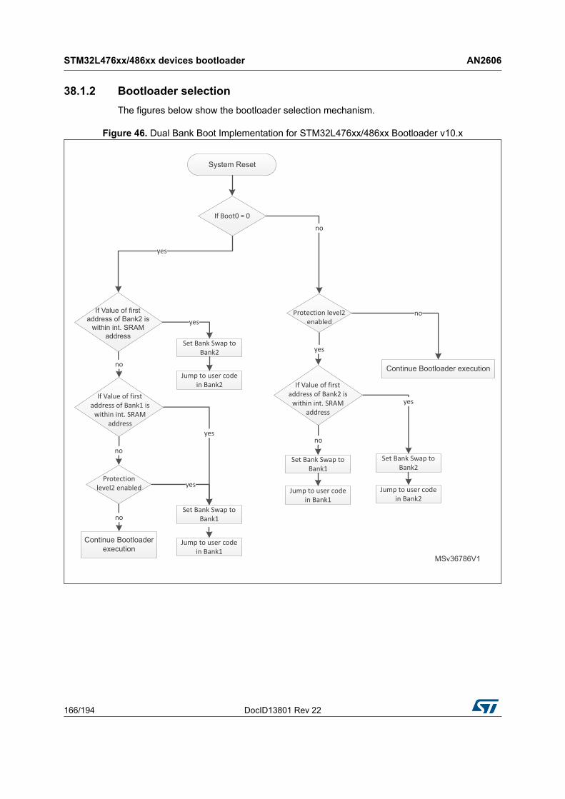
STM32L476xx/486xx devices bootloader AN2606
166/194 DocID13801 Rev 22
38.1.2 Bootloader selection
The figures below show the bootloader selection mechanism.
Figure 46. Dual Bank Boot Implementation for STM32L476xx/486xx Bootloader v10.x

DocID13801 Rev 22 167/194
AN2606 STM32L476xx/486xx devices bootloader
193
Figure 47.Bootloader V10.x selection for STM32L476xx/486xx

STM32L476xx/486xx devices bootloader AN2606
168/194 DocID13801 Rev 22
38.1.3 Bootloader version
The following table lists the STM32L476xx/486xx devices bootloader V10.x versions:
Table 83. STM32L476xx/486xx bootloader V10.x versions
Bootloader version number
Description Known limitations
V10.0 Deprecated version (not used) None
V10.1 Initial bootloader version Write in SRAM is corrupted
V10.2 Fix write in SRAM issue None
V10.3
Add support of MSI as USB clock source (MSI is trimmed by LSE).
Update dual bank boot feature to support the case when user stack
is mapped in SRAM2.
None
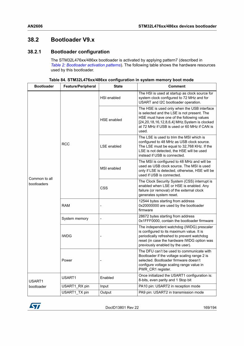
DocID13801 Rev 22 169/194
AN2606 STM32L476xx/486xx devices bootloader
193
38.2 Bootloader V9.x
38.2.1 Bootloader configuration
The STM32L476xx/486xx bootloader is activated by applying pattern7 (described in Table 2: Bootloader activation patterns). The following table shows the hardware resources used by this bootloader.
Table 84. STM32L476xx/486xx configuration in system memory boot mode
Bootloader Feature/Peripheral State Comment
Common to all
bootloaders
RCC
HSI enabledThe HSI is used at startup as clock source for system clock configured to 72 MHz and for USART and I2C bootloader operation.
HSE enabled
The HSE is used only when the USB interface is selected and the LSE is not present. The HSE must have one of the following values [24,20,18,16,12,8,6,4] MHz.System is clocked at 72 MHz if USB is used or 60 MHz if CAN is used.
LSE enabled
The LSE is used to trim the MSI which is configured to 48 MHz as USB clock source. The LSE must be equal to 32,768 KHz. If the LSE is not detected, the HSE will be used instead if USB is connected.
MSI enabled
The MSI is configured to 48 MHz and will be used as USB clock source. The MSI is used only if LSE is detected, otherwise, HSE will be used if USB is connected.
CSS
The Clock Security System (CSS) interrupt is enabled when LSE or HSE is enabled. Any failure (or removal) of the external clock generates system reset.
RAM -12544 bytes starting from address 0x20000000 are used by the bootloader firmware
System memory -28672 bytes starting from address 0x1FFF0000, contain the bootloader firmware
IWDG -
The independent watchdog (IWDG) prescaler is configured to its maximum value. It is periodically refreshed to prevent watchdog reset (in case the hardware IWDG option was previously enabled by the user).
Power -
The DFU can’t be used to communicate with Bootloader if the voltage scaling range 2 is selected. Bootloader firmware doesn’t configure voltage scaling range value in PWR_CR1 register.
USART1
bootloader
USART1 EnabledOnce initialized the USART1 configuration is: 8-bits, even parity and 1 Stop bit
USART1_RX pin Input PA10 pin: USART2 in reception mode
USART1_TX pin Output PA9 pin: USART2 in transmission mode

STM32L476xx/486xx devices bootloader AN2606
170/194 DocID13801 Rev 22
USART2
bootloader
USART2 EnabledOnce initialized the USART2 configuration is: 8-bits, even parity and 1 Stop bit
USART2_RX pin Input PA3 pin: USART2 in reception mode
USART2_TX pin Output PA2 pin: USART2 in transmission mode
USART3
bootloader
USART3 Enabled Once initialized the USART3 configuration is: 8-bits, even parity and 1 Stop bit
USART3_RX pin Input PC11 pin: USART3 in reception mode
USART3_TX pin Output PC10 pin: USART3 in transmission mode
USART1, USART2 and USART3
bootloaders
SysTick timer EnabledUsed to automatically detect the serial baud rate from the host for USARTx bootloaders.
I2C1 bootloader
I2C1 Enabled
The I2C1 configuration is:
I2C speed: up to 400 KHz, 7-bit address, slave mode, analog filter ON. Slave 7-bit address: 0b1000011x (where x = 0 for write and x = 1 for read)
I2C1_SCL pin Input/Output PB6 pin: clock line is used in open-drain mode.
I2C1_SDA pin Input/Output PB7 pin: data line is used in open-drain mode.
I2C2 bootloader
I2C2 Enabled
The I2C2 configuration is:
I2C speed: up to 400 KHz, 7-bit address, slave mode, analog filter ON. Slave 7-bit address: 0b1000011x (where x = 0 for write and x = 1 for read)
I2C2_SCL pin Input/Output PB10 pin: clock line is used in open-drain mode.
I2C2_SDA pin Input/Output PB11 pin: data line is used in open-drain mode.
I2C3 bootloader
I2C3 Enabled
The I2C3 configuration is:
I2C speed: up to 400 KHz, 7-bit address, slave mode, analog filter ON. Slave 7-bit address: 0b1000011x (where x = 0 for write and x = 1 for read)
I2C3_SCL pin Input/Output PC0 pin: clock line is used in open-drain mode.
I2C3_SDA pin Input/Output PC1 pin: data line is used in open-drain mode.
Table 84. STM32L476xx/486xx configuration in system memory boot mode (continued)
Bootloader Feature/Peripheral State Comment
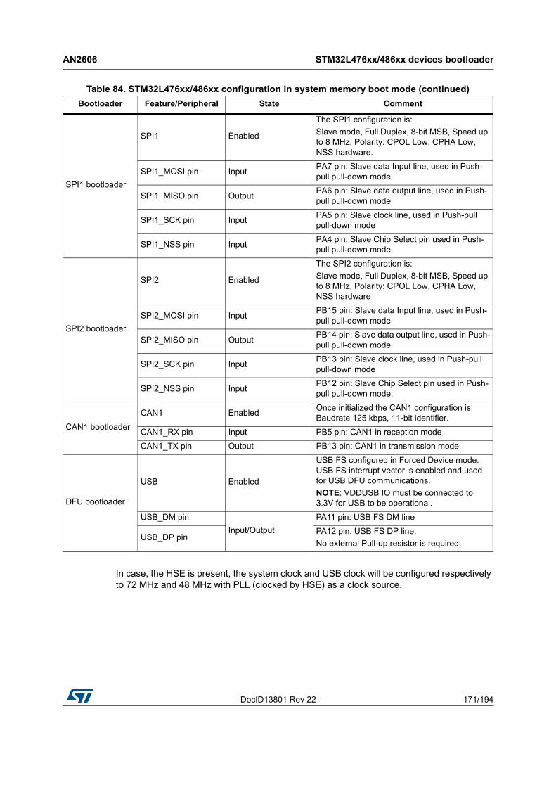
DocID13801 Rev 22 171/194
AN2606 STM32L476xx/486xx devices bootloader
193
In case, the HSE is present, the system clock and USB clock will be configured respectively to 72 MHz and 48 MHz with PLL (clocked by HSE) as a clock source.
SPI1 bootloader
SPI1 Enabled
The SPI1 configuration is:
Slave mode, Full Duplex, 8-bit MSB, Speed up to 8 MHz, Polarity: CPOL Low, CPHA Low, NSS hardware.
SPI1_MOSI pin Input PA7 pin: Slave data Input line, used in Push-pull pull-down mode
SPI1_MISO pin Output PA6 pin: Slave data output line, used in Push-pull pull-down mode
SPI1_SCK pin Input PA5 pin: Slave clock line, used in Push-pull pull-down mode
SPI1_NSS pin Input PA4 pin: Slave Chip Select pin used in Push-pull pull-down mode.
SPI2 bootloader
SPI2 Enabled
The SPI2 configuration is:
Slave mode, Full Duplex, 8-bit MSB, Speed up to 8 MHz, Polarity: CPOL Low, CPHA Low, NSS hardware
SPI2_MOSI pin Input PB15 pin: Slave data Input line, used in Push-pull pull-down mode
SPI2_MISO pin Output PB14 pin: Slave data output line, used in Push-pull pull-down mode
SPI2_SCK pin Input PB13 pin: Slave clock line, used in Push-pull pull-down mode
SPI2_NSS pin Input PB12 pin: Slave Chip Select pin used in Push-pull pull-down mode.
CAN1 bootloader
CAN1 Enabled Once initialized the CAN1 configuration is: Baudrate 125 kbps, 11-bit identifier.
CAN1_RX pin Input PB5 pin: CAN1 in reception mode
CAN1_TX pin Output PB13 pin: CAN1 in transmission mode
DFU bootloader
USB Enabled
USB FS configured in Forced Device mode. USB FS interrupt vector is enabled and used for USB DFU communications.
NOTE: VDDUSB IO must be connected to 3.3V for USB to be operational.
USB_DM pin
Input/Output
PA11 pin: USB FS DM line
USB_DP pinPA12 pin: USB FS DP line.
No external Pull-up resistor is required.
Table 84. STM32L476xx/486xx configuration in system memory boot mode (continued)
Bootloader Feature/Peripheral State Comment
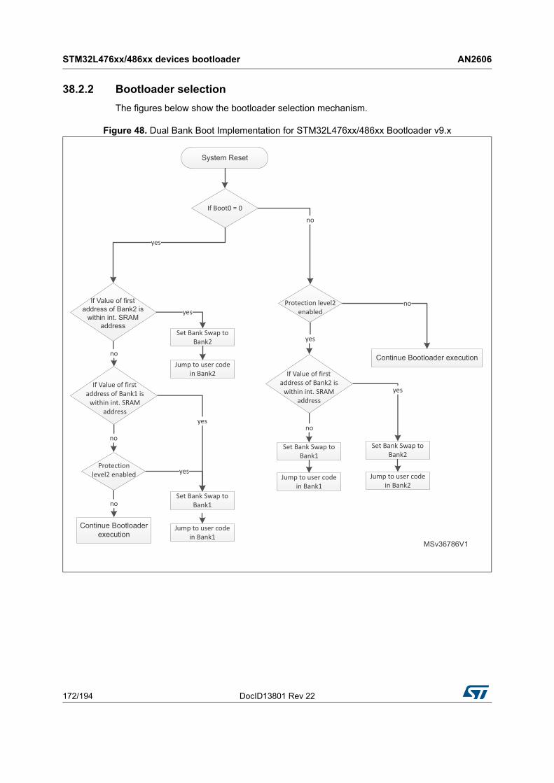
STM32L476xx/486xx devices bootloader AN2606
172/194 DocID13801 Rev 22
38.2.2 Bootloader selection
The figures below show the bootloader selection mechanism.
Figure 48. Dual Bank Boot Implementation for STM32L476xx/486xx Bootloader v9.x
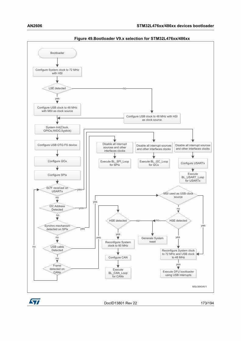
DocID13801 Rev 22 173/194
AN2606 STM32L476xx/486xx devices bootloader
193
Figure 49.Bootloader V9.x selection for STM32L476xx/486xx
STM32L476xx/486xx devices bootloader AN2606
174/194 DocID13801 Rev 22
38.2.3 Bootloader version
The following table lists the STM32L476xx/486xx devices bootloader V10.x versions:
Table 85. STM32L476xx/486xx bootloader V9.x versions
Bootloader version number
Description Known limitations
V9.0 Initial bootloader version None
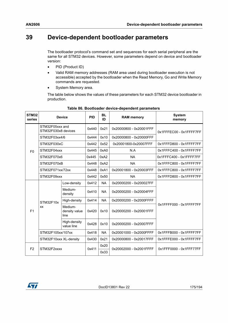
DocID13801 Rev 22 175/194
AN2606 Device-dependent bootloader parameters
193
39 Device-dependent bootloader parameters
The bootloader protocol’s command set and sequences for each serial peripheral are the same for all STM32 devices. However, some parameters depend on device and bootloader version:
• PID (Product ID)
• Valid RAM memory addresses (RAM area used during bootloader execution is not accessible) accepted by the bootloader when the Read Memory, Go and Write Memory commands are requested.
• System Memory area.
The table below shows the values of these parameters for each STM32 device bootloader in production.
Table 86. Bootloader device-dependent parameters
STM32series
Device PIDBL ID
RAM memorySystemmemory
F0
STM32F05xxx and STM32F030x8 devices
0x440 0x21 0x20000800 - 0x20001FFF0x1FFFEC00 - 0x1FFFF7FF
STM32F03xx4/6 0x444 0x10 0x20000800 - 0x20000FFF
STM32F030xC 0x442 0x52 0x20001800-0x20007FFF 0x1FFFD800 - 0x1FFFF7FF
STM32F04xxx 0x445 0xA0 N.A 0x1FFFC400 - 0x1FFFF7FF
STM32F070x6 0x445 0xA2 NA 0x1FFFC400 - 0x1FFFF7FF
STM32F070xB 0x448 0xA2 NA 0x1FFFC800 - 0x1FFFF7FF
STM32F071xx/72xx 0x448 0xA1 0x20001800 - 0x20003FFF 0x1FFFC800 - 0x1FFFF7FF
STM32F09xxx 0x442 0x50 NA 0x1FFFD800 - 0x1FFFF7FF
F1
STM32F10xxx
Low-density 0x412 NA 0x20000200 - 0x200027FF
0x1FFFF000 - 0x1FFFF7FF
Medium-density
0x410 NA 0x20000200 - 0x20004FFF
High-density 0x414 NA 0x20000200 - 0x2000FFFF
Medium-density value line
0x420 0x10 0x20000200 - 0x20001FFF
High-density value line
0x428 0x10 0x20000200 - 0x20007FFF
STM32F105xx/107xx 0x418 NA 0x20001000 - 0x2000FFFF 0x1FFFB000 - 0x1FFFF7FF
STM32F10xxx XL-density 0x430 0x21 0x20000800 - 0x20017FFF 0x1FFFE000 - 0x1FFFF7FF
F2 STM32F2xxxx 0x4110x20
0x20002000 - 0x2001FFFF 0x1FFF0000 - 0x1FFF77FF0x33

Device-dependent bootloader parameters AN2606
176/194 DocID13801 Rev 22
F3
STM32F373xx0x432
0x41 0x20001400 - 0x20007FFF
0x1FFFD800 - 0x1FFFF7FF
STM32F378xx 0x50 0x20001000 - 0x20007FFF
STM32F302xB(C)/303xB(C)0x422
0x410x20001400 - 0x20009FFF
STM32F358xx 0x50
STM32F301xx/302x4(6/8)0x439
0x400x20001800 - 0x20003FFF
STM32F318xx 0x50
STM32F303x4(6/8)/ 334xx/328xx
0x438 0x50 0x20001800 - 0x20002FFF
STM32F302xD(E)/303xD(E) 0x446 0x40 0x20001800 - 0x2000FFFF
STM32F398xx 0x446 0x50 0x20001800 - 0x2000FFFF
F4
STM32F40xxx/41xxx 0x4130x31 0x20002000 - 0x2001FFFF
0x1FFF0000 - 0x1FFF77FF
0x90 0x20003000 - 0x2001FFFF
STM32F42xxx/43xxx 0x4190x70
0x20003000 - 0x2002FFFF0x90
STM32F401xB(C) 0x423 0xD1 0x20003000 - 0x2000FFFF
STM32F401xD(E) 0x433 0xD1 0x20003000 - 0x20017FFF
STM32F411xx 0x431 0xD0 0x20003000 - 0x2001FFFF
STM32F446xx 0x421 0x90 0x20003000 - 0x2001FFFF
F7 STM32F74xxx/75xxx 0x4490x70 0x20004000 - 0x2004FFFF 0x1FF00000 - 0x1FF0EDBF
0x90 0x20004000 - 0x2004FFFF 0x1FF00000 - 0x1FF0EDBF
L0 STM32L05xxx/06xxx 0x417 0xC0 0x20001000 - 0x20001FFF
0x1FF00000 - 0x1FF00FFF
L1
STM32L1xxx6(8/B) 0x416 0x20 0x20000800 - 0x20003FFF
STM32L1xxx6(8/B)A 0x429 0x200x20001000 - 0x20007FFF
STM32L1xxxC 0x427 0x40
0x1FF00000 - 0x1FF01FFFSTM32L1xxxD 0x436 0x45 0x20001000 - 0x2000BFFF
STM32L1xxxE 0x437 0x40 0x20001000 - 0x20013FFF
L4 STM32L476xx/486xx 0x4150xA3 0x20003000 - 0x20017FFF
0x1FFF0000 - 0x1FFF6FFF0x90 0x20003100 - 0x20017FFF
Table 86. Bootloader device-dependent parameters (continued)
STM32series
Device PIDBL ID
RAM memorySystemmemory

DocID13801 Rev 22 177/194
AN2606 Bootloader timing
193
40 Bootloader timing
This section presents the typical timings of the bootloader firmware that should be used to ensure correct synchronization between host and STM32 device.
Two types of timings will be described herein:
• STM32 device bootloader resources initialization duration.
• Communication interface selection duration.
After these timings the bootloader is ready to receive and execute host commands.
40.1 Bootloader Startup timing
After bootloader reset, the host should wait until the STM32 bootloader is ready to start detection phase with a specific interface communication. This time corresponds to bootloader startup timing, during which resources used by bootloader are initialized.
Figure 50. Bootloader Startup timing description
The table below contains the minimum startup timing for each STM32 product:
Table 87. Bootloader startup timings of STM32 devices
DeviceMinimum
bootloader Startup (ms)
HSE Timeout (ms)
STM32F03xx4/6 1.612 N.A
STM32F05xxx and STM32F030x8 devices 1.612 N.A
STM32F04xxx 0.058 N.A
STM32F071xx/72xx 0.058 N.A
STM32F070x6HSE connected 3
200HSE not connected 230
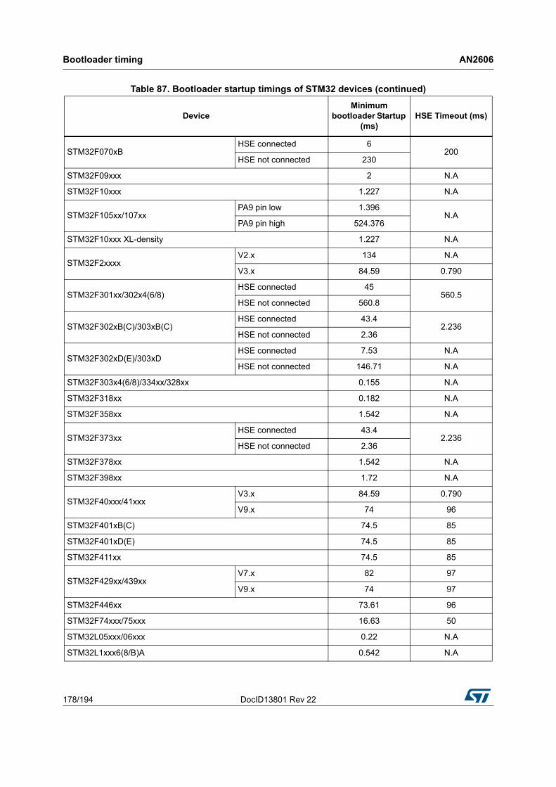
Bootloader timing AN2606
178/194 DocID13801 Rev 22
STM32F070xBHSE connected 6
200HSE not connected 230
STM32F09xxx 2 N.A
STM32F10xxx 1.227 N.A
STM32F105xx/107xx PA9 pin low 1.396
N.APA9 pin high 524.376
STM32F10xxx XL-density 1.227 N.A
STM32F2xxxxV2.x 134 N.A
V3.x 84.59 0.790
STM32F301xx/302x4(6/8) HSE connected 45
560.5HSE not connected 560.8
STM32F302xB(C)/303xB(C)HSE connected 43.4
2.236HSE not connected 2.36
STM32F302xD(E)/303xDHSE connected 7.53 N.A
HSE not connected 146.71 N.A
STM32F303x4(6/8)/334xx/328xx 0.155 N.A
STM32F318xx 0.182 N.A
STM32F358xx 1.542 N.A
STM32F373xxHSE connected 43.4
2.236HSE not connected 2.36
STM32F378xx 1.542 N.A
STM32F398xx 1.72 N.A
STM32F40xxx/41xxxV3.x 84.59 0.790
V9.x 74 96
STM32F401xB(C) 74.5 85
STM32F401xD(E) 74.5 85
STM32F411xx 74.5 85
STM32F429xx/439xxV7.x 82 97
V9.x 74 97
STM32F446xx 73.61 96
STM32F74xxx/75xxx 16.63 50
STM32L05xxx/06xxx 0.22 N.A
STM32L1xxx6(8/B)A 0.542 N.A
Table 87. Bootloader startup timings of STM32 devices (continued)
DeviceMinimum
bootloader Startup (ms)
HSE Timeout (ms)
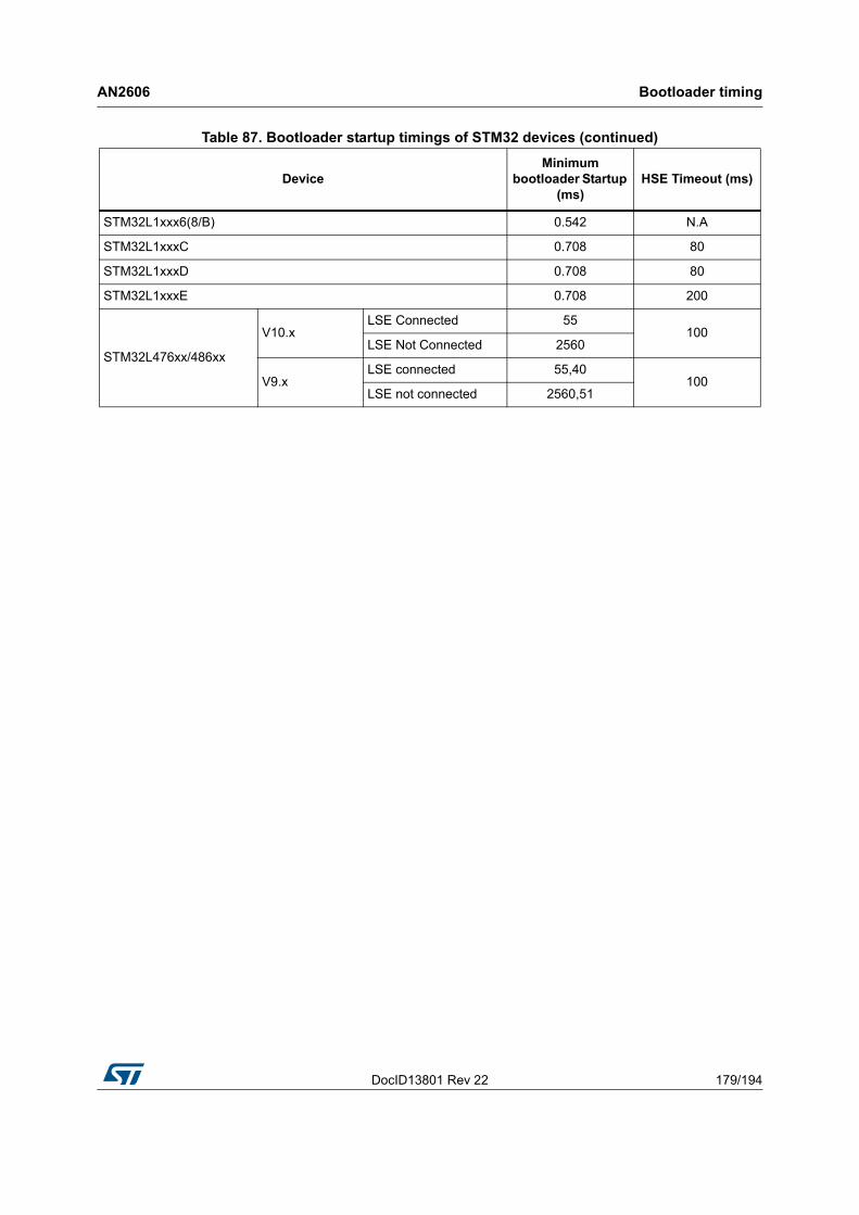
DocID13801 Rev 22 179/194
AN2606 Bootloader timing
193
STM32L1xxx6(8/B) 0.542 N.A
STM32L1xxxC 0.708 80
STM32L1xxxD 0.708 80
STM32L1xxxE 0.708 200
STM32L476xx/486xx
V10.xLSE Connected 55
100LSE Not Connected 2560
V9.xLSE connected 55,40
100LSE not connected 2560,51
Table 87. Bootloader startup timings of STM32 devices (continued)
DeviceMinimum
bootloader Startup (ms)
HSE Timeout (ms)

Bootloader timing AN2606
180/194 DocID13801 Rev 22
40.2 USART connection timing
USART connection timing is the time that the host should wait for between sending the synchronization data (0x7F) and receiving the first acknowledge response (0x79).
Figure 51. USART connection timing description
1. Receiving any other character different from 0x7F (or line glitches) will cause Bootloader to start communication using a wrong baudrate. Bootloader measures the signal length between rising edge of first 1 bit in 0x7F to the falling edge of the last 1 bit in 0x7F to deduce the baudrate value
2. Bootloader does not re-align the calculated baudrate to standard baudrate values (ie. 1200, 9600, 115200, ...).
Note: For STM32F105xx/107xx line devices, PA9 pin (USB_VBUS) is used to detect the USB host connection. The initialization of USB peripheral is performed only if PA9 is high at detection phase which means that a host is connected to the port and delivering 5 V on the USB bus. When PA9 level is high at detection phase, more time is required to initialize and shutdown the USB peripheral. To minimize bootloader detection time when PA9 pin is not used, keep PA9 state low during USART detection phase from the moment the device is reset till a device ACK is sent.
Table 88. USART bootloader minimum timings of STM32 devices
DeviceOne USART byte
sending (ms)
USART configuration
(ms)
USART connection (ms)
STM32F03xx4/6 0.078125 0.0064 0.16265
STM32F05xxx and STM32F030x8 devices 0.078125 0.0095 0.16575
STM32F04xxx 0.078125 0.007 0.16325
STM32F071xx/72xx 0.078125 0.007 0.16325
STM32F070x6 0.078125 0.014 0.17
STM32F070xB 0.078125 0.08 0.23

DocID13801 Rev 22 181/194
AN2606 Bootloader timing
193
STM32F09xxx 0.078125 0.07 0.22
STM32F10xxx 0.078125 0.002 0.15825
STM32F105xx/107xx PA9 pin low
0.0781250.007 0.16325
PA9 pin High 105 105.15625
STM32F10xxx XL-density 0.078125 0.006 0.16225
STM32F2xxxxV2.x
0.078125 0.009 0.16525V3.x
STM32F301xx/302x4(6/8) HSE connected
0.078125 0.002 0.15825HSE not connected
STM32F302xB(C)/303xB(C)HSE connected
0.078125 0.002 0.15825HSE not connected
STM32F302xD(E)/303xD 0.078125 0.002 0.15885
STM32F303x4(6/8)/334xx/328xx 0.078125 0.002 0.15825
STM32F318xx 0.078125 0.002 0.15825
STM32F358xx 0.15625 0.001 0.3135
STM32F373xxHSE connected
0.078125 0.002 0.15825HSE not connected
STM32F378xx 0.15625 0.001 0.3135
STM32F398xx 0.078125 0.002 0.15885
STM32F40xxx/41xxxV3.x
0.0781250.009 0.16525
V9.x 0.0035 0.15975
STM32F401xB(C) 0.078125 0.00326 0.15951
STM32F401xD(E) 0.078125 0.00326 0.15951
STM32F411xx 0.078125 0.00326 0.15951
STM32F429xx/439xxV7.x
0.0781250.007 0.16325
V9.x 0.00326 0.15951
STM32F446xx 0.078125 0.004 0.16
STM32F74xxx/75xxx 0.078125 0.065 50
STM32L05xxx/06xxx 0.078125 0.018 0.17425
STM32L1xxx6(8/B)A 0.078125 0.008 0.16425
STM32L1xxx6(8/B) 0.078125 0.008 0.16425
STM32L1xxxC 0.078125 0.008 0.16425
STM32L1xxxD 0.078125 0.008 0.16425
Table 88. USART bootloader minimum timings of STM32 devices (continued)
DeviceOne USART byte
sending (ms)
USART configuration
(ms)
USART connection (ms)

Bootloader timing AN2606
182/194 DocID13801 Rev 22
40.3 USB connection timing
USB connection timing is the time that the host should wait for between plugging the USB cable and establishing a correct connection with the device. This timing includes enumeration and DFU components configuration. USB connection depends on the host.
Figure 52. USB connection timing description
Note: For STM32F105xx/107xx devices, if the external HSE crystal frequency is different from 25 MHz (14.7456 MHz or 8 MHz), the device performs several unsuccessful enumerations (with connect – disconnect sequences) before being able to establish a correct connection with the host. This is due to the HSE automatic detection mechanism based on Start Of Frame (SOF) detection.
STM32L1xxxE 0.078125 0.008 0.16425
STM32L476xx/486xxV10.x 0.078125 0.003 0.159
V9.x 0.078125 0.003 0.159
Table 88. USART bootloader minimum timings of STM32 devices (continued)
DeviceOne USART byte
sending (ms)
USART configuration
(ms)
USART connection (ms)
Table 89. USB bootloader minimum timings of STM32 devices
Device USB connection (ms)
STM32F04xxx 350
STM32F070x6 TBD
STM32F070xB 320
STM32F105xx/107xx
HSE = 25 MHZ 460
HSE = 14.7465 MHZ 4500
HSE = 8 MHZ 13700
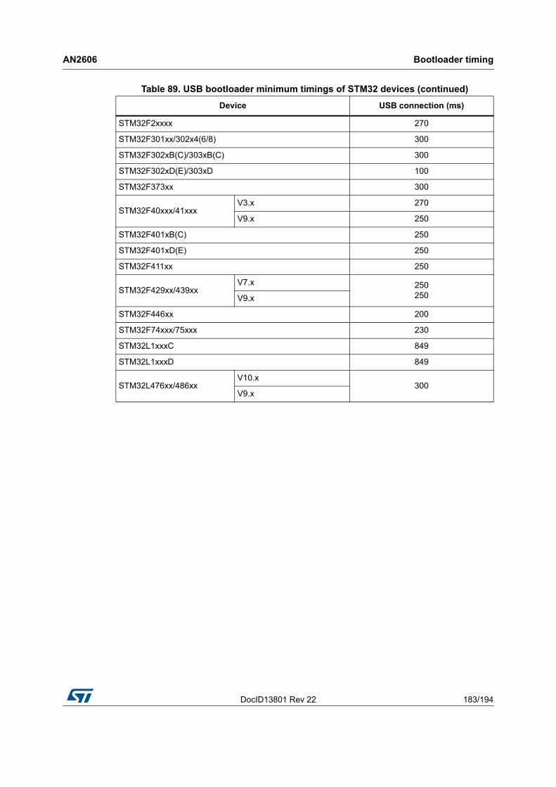
DocID13801 Rev 22 183/194
AN2606 Bootloader timing
193
STM32F2xxxx 270
STM32F301xx/302x4(6/8) 300
STM32F302xB(C)/303xB(C) 300
STM32F302xD(E)/303xD 100
STM32F373xx 300
STM32F40xxx/41xxxV3.x 270
V9.x 250
STM32F401xB(C) 250
STM32F401xD(E) 250
STM32F411xx 250
STM32F429xx/439xxV7.x 250
250V9.x
STM32F446xx 200
STM32F74xxx/75xxx 230
STM32L1xxxC 849
STM32L1xxxD 849
STM32L476xx/486xxV10.x
300V9.x
Table 89. USB bootloader minimum timings of STM32 devices (continued)
Device USB connection (ms)

Bootloader timing AN2606
184/194 DocID13801 Rev 22
40.4 I2C connection timing
I2C connection timing is the time that the host should wait for between sending I2C device address and sending command code. This timing includes I2C line stretching duration.
Figure 53. I2C connection timing description
Note: For I2C communication, a timeout mechanism is implemented and it must be respected to execute bootloader commands correctly. This timeout is implemented between two I2C frames in the same command (eg: for Write memory command a timeout is inserted between command sending frame and address memory sending frame). Also the same timeout period is inserted between two successive data reception or transmission in the same I2C frame. If the timeout period is elapsed a system reset is generated to avoid bootloader crash.
In erase memory command and read-out unprotect command, the duration of flash operation should be taken into consideration when implementing the host side. After sending the code of pages to be erased, the host should wait until the bootloader device performs page erasing to complete the remaining steps of erase command.
Table 90. I2C bootloader minimum timings of STM32 devices
DeviceStart condition + one I2C byte sending (ms)
I2C line stretching (ms)
I2C connection (ms)
I2C Timeout(ms)
STM32F04xxx 0.0225 0.0025 0.025 1000
STM32F071xx/72xx 0.0225 0.0025 0.025 1000
STM32F070x6 0.0225 0.002 0.245 1000
STM32F070xB 0.0225 0.002 0.245 1000
STM32F09xxx 0.0225 0.002 0.245 1000
STM32F74xxx/75xxx 0.0225 0.002 0.245 500

DocID13801 Rev 22 185/194
AN2606 Bootloader timing
193
STM32F303x4(6/8)/334xx/328xx 0.0225 0.0027 0.0252 1000
STM32F318xx 0.0225 0.0027 0.0252 1000
STM32F358xx 0.0225 0.0055 0.028 10
STM32F378xx 0.0225 0.0055 0.028 10
STM32F398xx 0.0225 0.002 0.245 1500
STM32F40xxx/41xxx 0.0225 0.0022 0.0247 1000
STM32F401xB(C) 0.0225 0022 0.0247 1000
STM32F401xD(E) 0.0225 0022 0.0247 1000
STM32F411xx 0.0225 0022 0.0247 1000
STM32F429xx/439xxV7.x
0.02250.0033 0.0258
1000V9.x 0.0022 0.0247
STM32F446xx 0.0225 0.002 0.245 1000
STM32L476xx/486xxV10.x 0.0225 0.002 0.245 1000
V9.x 0.0225 0.002 0.245 1000
Table 90. I2C bootloader minimum timings of STM32 devices (continued)
DeviceStart condition + one I2C byte sending (ms)
I2C line stretching (ms)
I2C connection (ms)
I2C Timeout(ms)
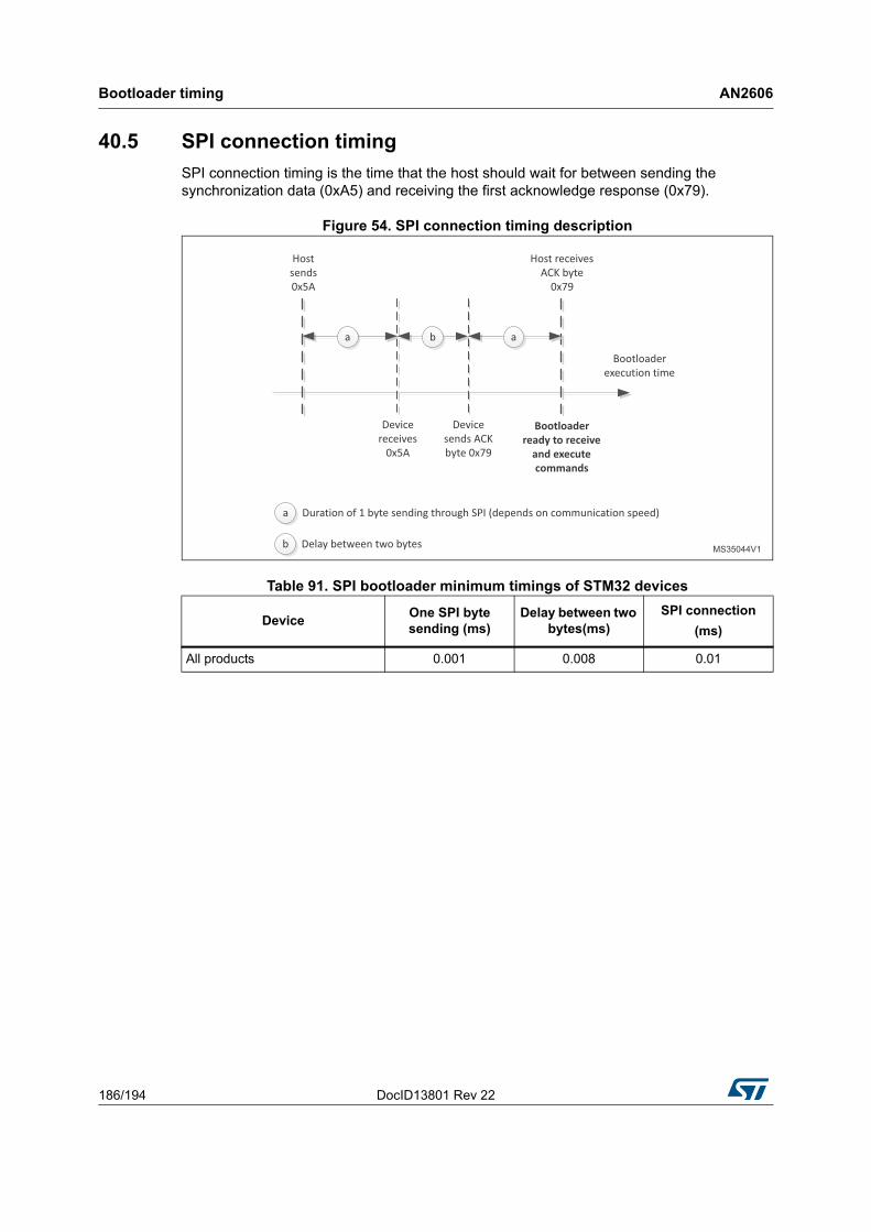
Bootloader timing AN2606
186/194 DocID13801 Rev 22
40.5 SPI connection timing
SPI connection timing is the time that the host should wait for between sending the synchronization data (0xA5) and receiving the first acknowledge response (0x79).
Figure 54. SPI connection timing description
Table 91. SPI bootloader minimum timings of STM32 devices
DeviceOne SPI byte sending (ms)
Delay between two bytes(ms)
SPI connection
(ms)
All products 0.001 0.008 0.01
DocID13801 Rev 22 187/194
AN2606 Revision history
193
41 Revision history
Table 92. Document revision history
Date Revision Changes
22-Oct-2007 1 Initial release.
22-Jan-2008 2
All STM32 in production (rev. B and rev. Z) include the bootloader described in this application note.
Modified: Section 3.1: Bootloader activation and Section 1.4: Bootloader code sequence.
Added: Section 1.3: Hardware requirements, Section 1.5: Choosing the USART baud rate, Section 1.6: Using the bootloader and Section:
Note 2 linked to Get, Get Version & Read Protection Status and Get ID commands in Table 3: Bootloader commands, Note 3 added.
Notion of “permanent” (Permanent Write Unprotect/Readout Protect/Unprotect) removed from document. Small text changes.
Bootloader version upgraded to 2.0.
26-May-2008 3
Small text changes. RAM and System memory added to Table : The system clock is derived from the embedded internal high-speed RC, no external quartz is required for the bootloader execution.
Section 1.6: Using the bootloader on page 8 removed.
Erase modified, Note 3 modified and Note 1 added in Table 3: Bootloader commands on page 9.
Byte 3: on page 11 modified.
Byte 2: on page 13 modified.
Byte 2:, Bytes 3-4: and Byte 5: on page 15 modified, Note 3 modified.
Byte 8: on page 18 modified.
Notes added to Section 2.5: Go command on page 18.
Figure 11: Go command: device side on page 20 modified.
Note added in Section 2.6: Write Memory command on page 21.
Byte 8: on page 24 modified.
Figure 14: Erase Memory command: host side and Figure 15: Erase Memory command: device side modified.
Byte 3: on page 26 modified.
Table 3: Bootloader commands on page 9.
Note modified and note added in Section 2.8: Write Protect command on page 27.
Figure 16: Write Protect command: host side, Figure 17: Write Protect command: device side, Figure 19: Write Unprotect command: device side, Figure 21: Readout Protect command: device side and Figure 23: Readout Unprotect command: device side modified.
29-Jan-2009 4This application note also applies to the STM32F102xx microcontrollers. Bootloader version updated to V2.2 (see Table 4: Bootloader versions).
Revision history AN2606
188/194 DocID13801 Rev 22
19-Nov-2009 5
IWDG added to Table : The system clock is derived from the embedded internal high-speed RC, no external quartz is required for the bootloader execution.. Note added.
BL changed bootloader in the entire document.
Go command description modified in Table : The system clock is derived from the embedded internal high-speed RC, no external quartz is required for the bootloader execution.
Number of bytes awaited by the bootloader corrected in Section 2.4: Read Memory command.
Note modified below Figure 10: Go command: host side.
Note removed in Section 2.5: Go command and note added.
Start RAM address specified and note added in Section 2.6: Write Memory command. All options are erased when a Write Memory command is issued to the Option byte area.
Figure 11: Go command: device side modified.
Figure 13: Write Memory command: device side modified.
Note added and bytes 3 and 4 sent by the host modified in Section 2.7: Erase Memory command.
Note added to Section 2.8: Write Protect command.
09-Mar-2010 6Application note restructured. Value line and connectivity line device bootloader added (Replaces AN2662).
Introduction changed. Glossary added.
20-Apr-2010 7
Related documents: added XL-density line datasheets and programming manual.
Glossary: added XL-density line devices.
Table 3: added information for XL-density line devices.
Section 4.1: Bootloader configuration: updated first sentence.
Section 5.1: Bootloader configuration: updated first sentence.
Added Section 6: STM32F10xxx XL-density devices bootloader.
Table 65: added information for XL-density line devices.
08-Oct-2010 8 Added information for high-density value line devices in Table 3 and Table 65.
14-Oct-2010 9 Removed references to obsolete devices.
26-Nov-2010 10 Added information on ultralow power devices.
13-Apr-2011 11Added information related to STM32F205/215xx and STM32F207/217xx devices.
Added Section 32: Bootloader timing
06-Jun-2011 12
Updated:
– Table 12: STM32L1xxx6(8/B) bootloader versions
– Table 17: STM32F2xxxx configuration in System memory boot mode
– Table 18: STM32F2xxxx bootloader V2.x versions
– Table 20: STM32F2xxxx bootloader V3.x versions
28-Nov-2011 13
Added information related to STM32F405/415xx and STM32F407/417xx bootloader, and STM32F105xx/107xx bootloader V2.1.
Added value line devices in Section 4: STM32F10xxx devices bootloader title and overview.
Table 92. Document revision history (continued)
Date Revision Changes
DocID13801 Rev 22 189/194
AN2606 Revision history
193
30-Jul-2012 14
Added information related to STM32F051x6/STM32F051x8 and to High-density ultralow power STM32L151xx, STM32L152xx bootloader.
Added case of BOOT1 bit in Section 3.1: Bootloader activation.
Updated Connectivity line, High-density ultralow power line, STM32F2xx and STM32F4xx in Table 3: Embedded bootloaders.
Added bootloader version V2.2 in Table 8: STM32F105xx/107xx bootloader versions.
Added bootloader V2.2 in Section 5.3.1: How to identify STM32F105xx/107xx bootloader versions.
Added note related to DFU interface below Table 15: STM32L1xxxx high-density configuration in System memory boot mode. Added V4.2 bootloader know limitations and updated description, and added V4.5 bootloader in Table 16: STM32L1xxxx high-density bootloader versions.
Added note related to DFU interface below Table 19: STM32F2xxxx configuration in System memory boot mode. Added V3.2 bootloader know limitations, and added V3.3 bootloader in Table 20: STM32F2xxxx bootloader V3.x versions. Updated STM32F2xx and STM32F4xx system memory end address in Table 21: STM32F40xxx/41xxx configuration in System memory boot mode.
Added note related to DFU interface below Table 21: STM32F40xxx/41xxx configuration in System memory boot mode. Added V3.0 bootloader know limitations, and added V3.1 bootloader in Table 22: STM32F40xxx/41xxx bootloader V3.x version.
Added bootloader V2.1 know limitations in Table 26: STM32F051xx bootloader versions.
Updated STM32F051x6/x8 system memory end address in Table 65: Bootloader device-dependent parameters.
Added Table 75: USART bootloader timings for high-density ultralow power devices, and Table 78: USART bootloader timings for STM32F051xx devices.
Added Table 88: USB minimum timings for high-density ultralow power devices.
Table 92. Document revision history (continued)
Date Revision Changes
Revision history AN2606
190/194 DocID13801 Rev 22
24-Jan-2013 15
Updated generic product names throughout the document (see Glossary).
Added the following new sections:
– Section 8: STM32L1xxxC devices bootloader.
– Section 13: STM32F031xx devices bootloader.
– Section 14: STM32F373xx devices bootloader.
– Section 15: STM32F302xB(C)/303xB(C) devices bootloader.
– Section 16: STM32F378xx devices bootloader.
– Section 17: STM32F358xx devices bootloader.
– Section 18: STM32F427xx/437xx devices bootloader.
– Section 34.3: I2C bootloader timing characteristics.
Updated Section 1: Related documents and Section 2: Glossary.
Added Table 79 to Table 85 (USART bootloader timings).
Replaced Figure 6 to Figure 16, and Figures 18, 19 and 42.
Modified Tables 3, 5, 9, 11, 17, 20, 21, 22 to 13, 27, 29, 31, 33, 35, 37 and 65.
Removed “X = 6: one USART is used” in Section 3.3: Hardware connection requirement.
Replaced address 0x1FFFF 8002 with address 0x1FFF F802 in Section 12.1: Bootloader configuration.
Modified procedure related to execution of the bootloader code in Note: on page 28, in Section 6.2: Bootloader selection and in Section 9.2: Bootloader selection.
06-Feb-2013 16
Added information related to I2C throughout the document.
Streamlined Table 1: Applicable products and Section 1: Related documents.
Modified Table 3: Embedded bootloaders as follows:
– Replaced "V6.0" with "V1.0"
– Replaced "0x1FFFF7A6" with "0x1FFFF796" in row STM32F31xx
– Replaced "0x1FFF7FA6" with "0x1FFFF7A6" in row STM32F051xx
Updated figures 6, 9 and 11.
Added Note: in Glossary and Note: in Section 3.1: Bootloader activation.
Replaced:
– "1.62 V" with "1.8 V" in tables17, 19, 19, 22, 21, 27, 37 and 59
– "5 Kbytes" with "4 Kbytes" in row RAM of Table 33
– "127 pages (2 KB each)" with "4 KB (2 pages of 2 KB each)" in rows F3 of Table 65
– "The bootloader ID is programmed in the last two bytes of the device system memory" with "The bootloader ID is programmed in the last byte address - 1 of the device system memory" in Section 3.3: Hardware connection requirement.
– "STM32F2xxxx devices revision Y" by "STM32F2xxxx devices revision X and Y" in Section 10: STM32F2xxxx devices bootloader
– “Voltage Range 2” with “Voltage Range 1” in tables 11, 15 and 26.
Table 92. Document revision history (continued)
Date Revision Changes
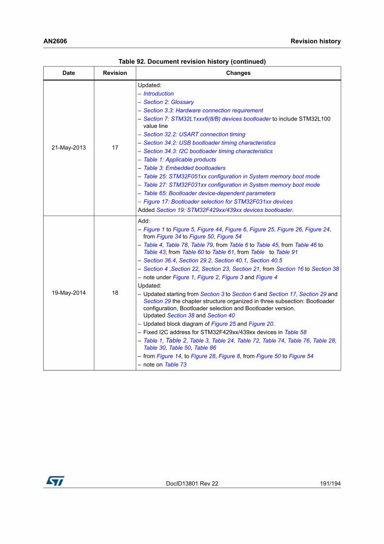
DocID13801 Rev 22 191/194
AN2606 Revision history
193
21-May-2013 17
Updated:
– Introduction
– Section 2: Glossary
– Section 3.3: Hardware connection requirement
– Section 7: STM32L1xxx6(8/B) devices bootloader to include STM32L100 value line
– Section 32.2: USART connection timing
– Section 34.2: USB bootloader timing characteristics
– Section 34.3: I2C bootloader timing characteristics
– Table 1: Applicable products
– Table 3: Embedded bootloaders
– Table 25: STM32F051xx configuration in System memory boot mode
– Table 27: STM32F031xx configuration in System memory boot mode
– Table 65: Bootloader device-dependent parameters
– Figure 17: Bootloader selection for STM32F031xx devices
Added Section 19: STM32F429xx/439xx devices bootloader.
19-May-2014 18
Add:
– Figure 1 to Figure 5, Figure 44, Figure 6, Figure 25, Figure 26, Figure 24, from Figure 34 to Figure 50, Figure 54
– Table 4, Table 78, Table 79, from Table 6 to Table 45, from Table 46 to Table 43, from Table 60 to Table 61, from Table to Table 91
– Section 36.4, Section 29.2, Section 40.1, Section 40.5
– Section 4 ,Section 22, Section 23, Section 21, from Section 16 to Section 38
– note under Figure 1, Figure 2, Figure 3 and Figure 4
Updated:
– Updated starting from Section 3 to Section 6 and Section 17, Section 29 and Section 29 the chapter structure organized in three subsection: Bootloader configuration, Bootloader selection and Bootloader version. Updated Section 38 and Section 40
– Updated block diagram of Figure 25 and Figure 20.
– Fixed I2C address for STM32F429xx/439xx devices in Table 58
– Table 1, Table 2, Table 3, Table 24, Table 72, Table 74, Table 76, Table 28, Table 30, Table 50, Table 86
– from Figure 14, to Figure 28, Figure 8, from Figure 50 to Figure 54
– note on Table 73
Table 92. Document revision history (continued)
Date Revision Changes

Revision history AN2606
192/194 DocID13801 Rev 22
29-Jul-2014 19
Updated:
– notes under Table 2
– Figure 43 and Figure 45
– Section 2: Glossary
– replaced any reference to STM32F427xx/437xx with STM32F42xxx/43xxx on Section 29: STM32F42xxx/43xxx devices bootloader
– replace any occurrence of ‘STM32F072xx’ with ‘STM32F07xxx’
– replace any occurrence of ‘STM32F051xx’ with ‘STM32F051xx and STM32F030x8 devices’.
– comment field related to OTG_FS_DP and OTG_FS_DM on Table 24, Table 30, Table 50, Table 78, Table 58, Table 60, Table 12, Table 18, Table 52, Table 54 and Table 56
– comment field related to USB_DM on Table 80.
– replace reference to "STM32F429xx/439xx" by "STM32F42xxx/43xxx” on Table 3
– comment field related to SPI2_MOSI, SPI2_MISO, SPI2_SCK and SPI2_NSS pins on Table 60
Added:
– note under Table 2
– reference to STM32F411 on Table 1, Section 2: Glossary, Table 87, Table 88, Table 89, Table 90
– Section 28: STM32F411xx devices bootloader
Removed reference to STM32F427xx/437xx on Table 3, Section 2: Glossary, Table 86, Table 87, Table 88, Table 89
24-Nov-2014 20
Updated:
– comment in “SPI1_NSS pin" and "SPI2_NSS pin" rows on Table 78 and Table 68
– comment in "SPI1_NSS pin", "SPI2_NSS pin" and "SPI3_NSS pin" rows on Table 52, Table 54 and Table 56
– Figure 1
Table 92. Document revision history (continued)
Date Revision Changes

DocID13801 Rev 22 193/194
AN2606 Revision history
193
11-Mar-2015 21
Updated:
– Table 1, Table 3, Table 22, Table 26, Table 72, Table 28, Table 30, Table 31, Table 50, Table 78, Table 10, Table 11, Table 6, Table 34, Table 58, Table 60, Table 12, Table 13, Table 18, Table 19,Table 32, Table 70, Table 82, Table 86, Table 87, Table 88, Table 89 and Table 90
– Figure 47
– Chapter 2: Glossary
– Section 3.1 and Section 3.4
Added:
– Section 38: STM32L476xx/486xx devices bootloader and Section 30: STM32F446xx devices bootloader
09-Jun-2015 22
Added:
– Section 8: STM32F070x6 devices bootloader
– Section 9: STM32F070xB devices bootloader
– Section 11: STM32F09xxx devices bootloader
– Section 18: STM32F302xD(E)/303xD(E) devices bootloaderSection 24: STM32F398xx devices bootloader
– Section 31: STM32F74xxx/75xxx devices bootloader
– Section 38.2: Bootloader V9.x
– Notes 1 and 2 on Figure 51
Updated:
– Table 1
– Section 2: Glossary
– Table 2
– Table 3
– Section 3.4: Bootloader Memory Management
– Table 86, Table 87, Table 88, Table 89 and Table 90
Table 92. Document revision history (continued)
Date Revision Changes

AN2606
194/194 DocID13801 Rev 22
IMPORTANT NOTICE – PLEASE READ CAREFULLY
STMicroelectronics NV and its subsidiaries (“ST”) reserve the right to make changes, corrections, enhancements, modifications, and improvements to ST products and/or to this document at any time without notice. Purchasers should obtain the latest relevant information on ST products before placing orders. ST products are sold pursuant to ST’s terms and conditions of sale in place at the time of order acknowledgement.
Purchasers are solely responsible for the choice, selection, and use of ST products and ST assumes no liability for application assistance or the design of Purchasers’ products.
No license, express or implied, to any intellectual property right is granted by ST herein.
Resale of ST products with provisions different from the information set forth herein shall void any warranty granted by ST for such product.
ST and the ST logo are trademarks of ST. All other product or service names are the property of their respective owners.
Information in this document supersedes and replaces information previously supplied in any prior versions of this document.
© 2015 STMicroelectronics – All rights reserved