AN1541/D Introduction to Insulated Gate Bipolar...
12
1 AN1541/D Introduction to Insulated Gate Bipolar Transistors Prepared by: Jack Takesuye and Scott Deuty Motorola Inc. INTRODUCTION As power conversion relies more on switched applications, semiconductor manufacturers need to create products that approach the ideal switch. The ideal switch would have: 1) zero resistance or forward voltage drop in the on−state, 2) infinite resistance in the off−state, 3) switch with infinite speed, and 4) would not require any input power to make it switch. When using existing solid−state switch technologies, the designer must deviate from the ideal switch and choose a device that best suits the application with a minimal loss of efficiency. The choice involves considerations such as voltage, current, switching speed, drive circuitry, load, and temperature effects. There are a variety of solid state switch technologies available to perform switching functions; however, all have strong and weak points. HIGH VOLTAGE POWER MOSFETs The primary characteristics that are most desirable in a solid−state switch are fast switching speed, simple drive requirements and low conduction loss. For low voltage applications, power MOSFETs offer extremely low on−resistance, R DS(on) , and approach the desired ideal switch. In high voltage applications, MOSFETs exhibit increased R DS(on) resulting in lower efficiency due to increased conduction losses. In a power MOSFET, the on−resistance is proportional to the breakdown voltage raised to approximately the 2.7 power (1). MOSFET technology has advanced to a point where cell densities are limited by manufacturing equipment capabilities and geometries have been optimized to a point where the R DS(on) is near the predicted theoretical limit. Since the cell density, geometry and the resistivity of the device structure play a major role, no significant reduction in the R DS(on) is foreseen. New technologies are needed to circumvent the problem of increased on−resistance without sacrificing switching speed. R DS(on) V 2.7 DSS (1) ENTER THE IGBT By combining the low conduction loss of a BJT with the switching speed of a power MOSFET an optimal solid state switch would exist. The I nsulated−G ate B ipolar T ransistor (IGBT) technology offers a combination of these attributes. The IGBT is, in fact, a spin−off from power MOSFET technology and the structure of an IGBT closely resembles that of a power MOSFET. The IGBT has high input impedance and fast turn−on speed like a MOSFET. IGBTs exhibit an on−voltage and current density comparable to a bipolar transistor while switching much faster. IGBTs are replacing MOSFETs in high voltage applications where conduction losses must be kept low. With zero current switching or resonant switching techniques, the IGBT can be operated in the hundreds of kilohertz range [ 1.]. Although turn−on speeds are very fast, turn−off of the IGBT is slower than a MOSFET. The IGBT exhibits a current fall time or “tailing.” The tailing restricts the devices to operating at moderate frequencies (less than 50 kHz) in traditional “square waveform” PWM, switching applications. At operating frequencies between 1 and 50 kHz, IGBTs offer an attractive solution over the traditional bipolar transistors, MOSFETs and thyristors. Compared to thyristors, the IGBT is faster, has better dv/dt immunity and, above all, has better gate turn−off capability. While some thyristors such as GTOs are capable of being turned off at the gate, substantial reverse gate current is required, whereas turning off an IGBT only requires that the gate capacitance be discharged. A thyristor has a slightly lower forward−on voltage and higher surge capability than an IGBT. MOSFETs are often used because of their simple gate drive requirements. Since the structure of both devices are so similar, the change to IGBTs can be made without having to redesign the gate drive circuit. IGBTs, like MOSFETs, are transconductance devices and can remain fully on by keeping the gate voltage above a certain threshold. APPLICATION NOTE Littelfuse.com Specifications subject to change without notice. 2016 Littelfuse, Inc. September 19, 2016 - Rev. 2 Publication Order Number: AN1541/D
Transcript of AN1541/D Introduction to Insulated Gate Bipolar...

1
AN1541/D
Introduction to InsulatedGate Bipolar TransistorsPrepared by: Jack Takesuye and Scott Deuty
Motorola Inc.
INTRODUCTIONAs power conversion relies more on switched
applications, semiconductor manufacturers need to createproducts that approach the ideal switch. The ideal switchwould have: 1) zero resistance or forward voltage drop inthe on−state, 2) infinite resistance in the off−state, 3) switchwith infinite speed, and 4) would not require any inputpower to make it switch.
When using existing solid−state switch technologies, thedesigner must deviate from the ideal switch and choose adevice that best suits the application with a minimal loss ofefficiency. The choice involves considerations such asvoltage, current, switching speed, drive circuitry, load, andtemperature effects. There are a variety of solid state switchtechnologies available to perform switching functions;however, all have strong and weak points.
HIGH VOLTAGE POWER MOSFETsThe primary characteristics that are most desirable in a
solid−state switch are fast switching speed, simple driverequirements and low conduction loss. For low voltageapplications, power MOSFETs offer extremely lowon−resistance, RDS(on), and approach the desired idealswitch. In high voltage applications, MOSFETs exhibitincreased RDS(on) resulting in lower efficiency due toincreased conduction losses. In a power MOSFET, theon−resistance is proportional to the breakdown voltageraised to approximately the 2.7 power (1).
MOSFET technology has advanced to a point where celldensities are limited by manufacturing equipmentcapabilities and geometries have been optimized to a pointwhere the RDS(on) is near the predicted theoretical limit.Since the cell density, geometry and the resistivity of thedevice structure play a major role, no significant reductionin the RDS(on) is foreseen. New technologies are needed tocircumvent the problem of increased on−resistance withoutsacrificing switching speed.
RDS(on) V 2.7DSS (1)
ENTER THE IGBTBy combining the low conduction loss of a BJT with the
switching speed of a power MOSFET an optimal solid stateswitch would exist. The Insulated−Gate Bipolar Transistor(IGBT) technology offers a combination of these attributes.
The IGBT is, in fact, a spin−off from power MOSFETtechnology and the structure of an IGBT closely resemblesthat of a power MOSFET. The IGBT has high inputimpedance and fast turn−on speed like a MOSFET. IGBTsexhibit an on−voltage and current density comparable to abipolar transistor while switching much faster. IGBTs arereplacing MOSFETs in high voltage applications whereconduction losses must be kept low. With zero currentswitching or resonant switching techniques, the IGBT canbe operated in the hundreds of kilohertz range [ 1.].
Although turn−on speeds are very fast, turn−off of theIGBT is slower than a MOSFET. The IGBT exhibits acurrent fall time or “tailing.” The tailing restricts the devicesto operating at moderate frequencies (less than 50 kHz) intraditional “square waveform” PWM, switchingapplications.
At operating frequencies between 1 and 50 kHz, IGBTsoffer an attractive solution over the traditional bipolartransistors, MOSFETs and thyristors. Compared tothyristors, the IGBT is faster, has better dv/dt immunity and,above all, has better gate turn−off capability. While somethyristors such as GTOs are capable of being turned off at thegate, substantial reverse gate current is required, whereasturning off an IGBT only requires that the gate capacitancebe discharged. A thyristor has a slightly lower forward−onvoltage and higher surge capability than an IGBT.
MOSFETs are often used because of their simple gatedrive requirements. Since the structure of both devices areso similar, the change to IGBTs can be made without havingto redesign the gate drive circuit. IGBTs, like MOSFETs, aretransconductance devices and can remain fully on bykeeping the gate voltage above a certain threshold.
APPLICATION NOTE
Littelfuse.com
©Specifications subject to change without notice. 2016 Littelfuse, Inc.September 19, 2016 - Rev. 2
Publication Order Number:AN1541/D

AN1541/D
2
As shown in Figure 1a, using an IGBT in place of a powerMOSFET dramatically reduces the forward voltage drop atcurrent levels above 12 amps. By reducing the forward drop,the conduction loss of the device is decreased. The gradualrising slope of the MOSFET in Figure 1a can be attributedto the relationship of VDS to RDS(on). The IGBT curve hasan offset due to an internal forward biased p−n junction anda fast rising slope typical of a minority carrier device.
Figure 1.(b)Reduced Die Size of IGBT RealizedWhen Compared to a MOSFET with Similar Ratings
0.10
0.05
0 1A
REA
(SQ
. IN
CHES
)
IGBT DIE SIZE(0.17 X 0.227)
MOSFET DIE SIZE(0.35 X 0.26)
FORWARD DROP (VOLTS)
Figure 1. (a)Reduced Forward Voltage Drop ofIGBT Realized When Compared to a MOSFET
with Similar Ratings
40
35
30
25
20
15
10
5
0 1086420
PEA
K CU
RREN
T TH
ROU
GH
DEV
ICE
(AM
PS)
VCE(sat)MGW20N60D IGBT
VDS MTW20N50EMOSFET
0.60
0.20
0 1
ARE
A (S
Q. I
NCH
ES)
IGBT PACKAGESIZE (TO−220)
MOSFET PACKAGESIZE (T0−247)
0.40
Figure 1.(c)Reduced Package Size of IGBTRealized When Compared to a MOSFET withSimilar Ratings
It is possible to replace the MOSFET with an IGBT andimprove the efficiency and/or reduce the cost. As shown inFigure 1b, an IGBT has considerably less silicon area thana similarly rated MOSFET. Device cost is related to siliconarea; therefore, the reduced silicon area makes the IGBT thelower cost solution. Figure 1c shows the resulting packagearea reduction realized by using the IGBT. The IGBT ismore space efficient than an equivalently rated MOSFETwhich makes it perfect for space conscious designs.
When compared to BJTs, IGBTs have similar ratings interms of voltage and current. However, the presence of anisolated gate in an IGBT makes it simpler to drive than a BJT.BJTs require that base current be continuously supplied in a
quantity sufficient enough to maintain saturation. Basecurrents of one−tenth of the collector current are typical tokeep a BJT in saturation. BJT drive circuits must be sensitiveto variable load conditions. The base current of a BJT mustbe kept proportional to the collector current to preventdesaturation under high−current loads and excessive basedrive under low−load conditions. This additional basecurrent increases the power dissipation of the drive circuit.BJTs are minority carrier devices and charge storage effectsincluding recombination slow the performance whencompared to majority carrier devices such as MOSFETs.IGBTs also experience recombination that accounts for the
©Specifications subject to change without notice. 2016 Littelfuse, Inc.September 19, 2016 - Rev. 2
Publication Order Number:AN1541/D
AN1541/D
3
current “tailing” yet IGBTs have been observed to switchfaster than BJTs.
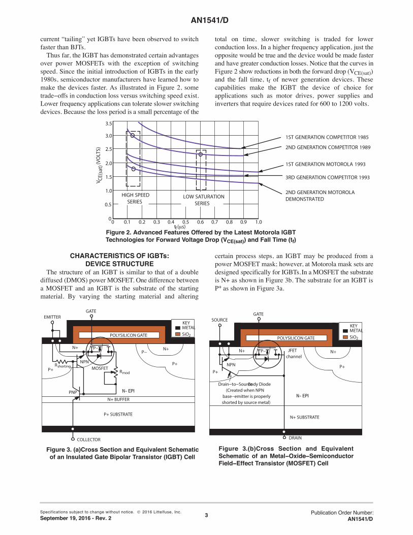
Thus far, the IGBT has demonstrated certain advantagesover power MOSFETs with the exception of switchingspeed. Since the initial introduction of IGBTs in the early1980s, semiconductor manufacturers have learned how tomake the devices faster. As illustrated in Figure 2, sometrade−offs in conduction loss versus switching speed exist.Lower frequency applications can tolerate slower switchingdevices. Because the loss period is a small percentage of the
total on time, slower switching is traded for lowerconduction loss. In a higher frequency application, just theopposite would be true and the device would be made fasterand have greater conduction losses. Notice that the curves inFigure 2 show reductions in both the forward drop (VCE(sat))and the fall time, tf of newer generation devices. Thesecapabilities make the IGBT the device of choice forapplications such as motor drives, power supplies andinverters that require devices rated for 600 to 1200 volts.
Figure 2. Advanced Features Offered by the Latest Motorola IGBTTechnologies for Forward Voltage Drop (VCE(sat)) and Fall Time (tf)
tf (μs)
3.5
3.0
2.5
2.0
1.5
1.0
0.5
0 1.00.80.60.40.2 9.00 0.70.50.3
1ST GENERATION COMPETITOR 1985
2ND GENERATION COMPETITOR 1989
1ST GENERATION MOTOROLA 1993
3RD GENERATION COMPETITOR 1993
2ND GENERATION MOTOROLADEMONSTRATED
V CE(s
at) (V
OLT
S)
HIGH SPEEDSERIES
LOW SATURATIONSERIES
0.1
CHARACTERISTICS OF IGBTs:DEVICE STRUCTURE
The structure of an IGBT is similar to that of a doublediffused (DMOS) power MOSFET. One difference betweena MOSFET and an IGBT is the substrate of the startingmaterial. By varying the starting material and altering
certain process steps, an IGBT may be produced from apower MOSFET mask; however, at Motorola mask sets aredesigned specifically for IGBTs. In a MOSFET the substrateis N+ as shown in Figure 3b. The substrate for an IGBT isP+ as shown in Figure 3a.
Figure 3. (a)Cross Section and Equivalent Schematicof an Insulated Gate Bipolar Transistor (IGBT) Cell
POLYSILICON GATE
N+
P+
N+ BUFFER
P+ SUBSTRATE
P−
Rmod
EMITTER
N+
P+
P−
COLLECTOR
GATE
NPNMOSFET
PNP
KEYMETALSiO2
Rshorting
Figure 3.(b)Cross Section and EquivalentSchematic of an Metal−Oxide−SemiconductorField−Effect Transistor (MOSFET) Cell
JFETchannel
Drain−to−Source Body Diode(Created when NPN
base−emitter is properlyshorted by source metal)
POLYSILICON GATE
N+
P+
N+ SUBSTRATE
SOURCE
N+
P+
DRAIN
NPN
GATE
P−
KEYMETALSiO2
©Specifications subject to change without notice. 2016 Littelfuse, Inc.September 19, 2016 - Rev. 2
Publication Order Number:AN1541/D

AN1541/D
4
The n− epi resistivity determines the breakdown voltageof a MOSFET as mentioned earlier using relationship (1).
RDS(on) V 2.7DSS (1)
To increase the breakdown voltage of the MOSFET, then− epi region thickness (vertical direction in figure) isincreased. As depicted in the classical resistancerelationship (2), reducing the RDS(on) of a high voltagedevice requires greater silicon area A to make up for theincreased n− epi region.
R 1A (2)
Device designers were challenged to overcome the effectsof the high resistive n− epi region. The solution to this camein the form of conductivity modulation. The n− epi region tothis was placed on the P+ substrate forming a p−n junctionwhere conductivity modulation takes place. Because ofconductivity modulation, the IGBT has a much greatercurrent density than a power MOSFET and the forwardvoltage drop is reduced. Now the P+ substrate, n− epi layerand P+ “emitter” form a BJT transistor and the n− epi acts asa wide base region.
The subject of current tailing has been mentioned severaltimes. Thus far, the device structure as shown in Figure 3provides insight as to what causes the tailing. Minoritycarriers build up to form the basis for conductivitymodulation. When the device turns off, these carriers do nothave a current path to exit the device. Recombination is theonly way to eliminate the stored charge resulting from thebuild−up of excess carriers. Additional recombinationcenters are formed by placing an N+ buffer layer between then− epi and P+ substrate.
While the N+ buffer layer may speed up therecombination, it also increases the forward drop of thedevice. Hence the tradeoff between switching speed andconduction loss becomes a factor in optimizing deviceperformance. Additional benefits of the N+ buffer layerinclude preventing thermal runaway and punch−through ofthe depletion region. This allows a thinner n− epi to be usedwhich somewhat decreases forward voltage drop.
The IGBT has a four layer (P−N−P−N) structure. Thisstructure resembles that of a thyristor device known as aSilicon Controlled Rectifier (SCR). Unlike the SCR wherethe device latches and gate control is lost, an IGBT isdesigned so that it does not latch on. Full control of thedevice can be maintained through the gate drive.
To maximize the performance of the IGBT, process stepsare optimized to control the geometry, doping and lifetime.The possibility of latching is also reduced by strategicprocessing of the device. Geometry and doping levels areoptimized to minimize the on−voltage, switching speed andachieve other key parametric variations. Because the IGBTis a four−layer structure, it does not have the inverse paralleldiode inherent to power MOSFETs. This is a disadvantage
to motor control designers who use the anti−parallel diodeto recover energy from the motor.
Like a power MOSFET, the gate of the IGBT iselectrically isolated from the rest of the chip by a thin layerof silicon dioxide, SiO2. The IGBT has a high inputimpedance due to the isolated gate and it exhibits theaccompanying advantages of modest gate driverequirements and excellent gate drive efficiency.
Equivalent Circuit of IGBTFigure 4b shows the terminals of the IGBT as determined
by JEDEC. Notice that the IGBT has a gate like a MOSFETyet it has an emitter and a collector like a BJT.
Figure 4. (a)IGBT Schematic Symbol
COLLECTOR
EMITTER
GATE
Figure 4.(b)MOSFET Schematic Symbol
GATE
SOURCE
DRAIN
The operation of the IGBT is best understood by againreferring to the cross section of the device and its equivalentcircuit as shown in Figure 3a. Current flowing from collectorto emitter must pass through a p−n junction formed by the P+
substrate and n− epi layer. This drop is similar to that seenin a forward biased p−n junction diode and results in anoffset voltage in the output characteristic. Current flowcontributions are shown in Figure 3a using varying linethickness with the thicker lines indicating a high currentpath. For a fast device, the N+ buffer layer is highly dopedfor recombination and speedy turn off. The additionaldoping keeps the gain of the PNP low and allows two−thirdsof the current to flow through the base of the PNP (electroncurrent) while one−third passes through the collector (holecurrent).
Rshorting is the parasitic resistance of the P+ emitter region.Current flowing through Rshorting can result in a voltageacross the base−emitter junction of the NPN. If thebase−emitter voltage is above a certain threshold level, theNPN will begin to conduct causing the NPN and PNP toenhance each other’s current flow and both devices canbecome saturated. This results in the device latching in afashion similar to an SCR. Device processing directs
©Specifications subject to change without notice. 2016 Littelfuse, Inc.September 19, 2016 - Rev. 2
Publication Order Number:AN1541/D

AN1541/D
5
currents within the device and keeps the voltage acrossRshorting low to avoid latching. The IGBT can be gated offunlike the SCR which has to wait for the current to ceaseallowing recombination to take place in order to turn off.IGBTs offer an advantage over the SCR by controlling thecurrent with the device, not the device with the current. Theinternal MOSFET of the IGBT when gated off will stopcurrent flow and at that point, the stored charges can only bedissipated through recombination.
The IGBT’s on−voltage is represented by sum of the offsetvoltage of the collector to base junction of the PNPtransistor, the voltage drop across the modulated resistanceRmod and the channel resistance of the internal MOSFET.Unlike the MOSFET where increased temperature results inincreased RDS(on) and increased forward voltage drop, theforward drop of an IGBT stays relatively unchanged atincreased temperatures.
Switching SpeedUntil recently, the feature that limited the IGBT from
serving a wide variety of applications was its relatively slowturn−off speed when compared to a power MOSFET. Whileturn−on is fairly rapid, initial IGBTs had current fall timesof around three microseconds.
The turn−off time of an IGBT is slow because manyminority carriers are stored in the n− epi region. When thegate is initially brought below the threshold voltage, then− epi contains a very large concentration of electrons andthere will be significant injection into the P+ substrate and acorresponding hole injection into the n− epi. As the electronconcentration in the n−region decreases, the electroninjection decreases, leaving the rest of the electrons torecombine. Therefore, the turn−off of an IGBT has twophases: an injection phase where the collector current fallsvery quickly, and a recombination phase in which thecollector current decrease more slowly. Figure 5 shows theswitching waveform and the tail time contributing factors ofa “fast” IGBT designed for PWM motor control service.
In power MOSFETs, the switching speed can be greatlyaffected by the impedance in the gate drive circuit. Effortsto minimize gate drive impedance for IGBTs are alsorecommended. Also, choose an optimal device based onswitching speed or use a slower device with lower forwarddrop and employ external circuitry to enhance turn off. Aturn−off mechanism is suggested in a paper by Baliga et al[ 2.].
Figure 5. IGBT Current Turn−off Waveform
6
5
4
3
2
1
0
−110008006004002000
I C (AM
PS)
TAIL TIME of MOTOROLA GEN. 2 IGBT #2 in1.0 hp MOTOR DRIVE at 1750 RPM
PNP TURN−OFFPORTION
TAIL TIME
MOSFET TURN−OFFPORTION
A FINAL COMPARISON OF IGBTs, BJTs ANDPOWER MOSFETs
The conduction losses of BJTs and IGBTs is related to theforward voltage drop of the device while MOSFETsdetermine conduction loss based on RDS(on). To get arelative comparison of turn−off time and conductionassociated losses, data is presented in Table 1 where theon−resistances of a power MOSFET, an IGBT and a BJT atjunction temperatures of 25°C and 150°C are shown.
Note that the devices in Table 1 have approximately thesame ratings. However, to achieve these ratings the chip sizeof the devices vary significantly. The bipolar transistorrequires 1.2 times more silicon area than the IGBT and theMOSFET requires 2.2 times the area of the IGBT to achievethe same ratings. This differences in die area directlyimpacts the cost of the product. At higher currents and atelevated temperatures, the IGBT offers low forward dropand a switching time similar to the BJT without the drivedifficulties. Table 1 confirms the findings offered earlier inFigure 1a and elaborates further to include a BJTcomparison and temperature effects. The reduced powerconduction losses offered by the IGBT lower powerdissipation and heat sink size.
Thermal ResistanceAn IGBT and power MOSFET produced from the same
size die have similar junction−to−case thermal resistancebecause of their similar structures. The thermal resistance ofa power MOSFET can be determined by testing for
©Specifications subject to change without notice. 2016 Littelfuse, Inc.September 19, 2016 - Rev. 2
Publication Order Number:AN1541/D

AN1541/D
6
variations in temperature sensitive parameters (TSPs).These parameters are the source−to−drain diode on−voltage,the gate−to−source threshold voltage, and thedrain−to−source on−resistance. All previous measurementsof thermal resistance of power MOSFETs at Motorola wereperformed using the source−to−drain diode as the TSP.Since an IGBT does not have an inverse parallel diode,another TSP had to be used to determine the thermalresistance. The gate−to−emitter threshold voltage was used
as the TSP to measure the junction temperature of an IGBTto determine its thermal resistance. However, before testingIGBTs, a correlation between the two test methods wasestablished by comparing the test results of MOSFETs usingboth TSPs. By testing for variations in threshold voltage, itwas determined that the thermal resistance of MOSFETs andIGBTs are essentially the same for devices with equivalentdie size.
Table 1. Advantages Offered by the IGBT When Comparing the MOSFET, IGBT and Bipolar TransistorOn−Resistances (Over Junction Temperature) and Fall Times (Resistance Values at 10 Amps of Current)
Characteristic TMOS IGBT Bipolar
Current Rating 20 A 20 A 20 A
Voltage Rating 500 V 600 V 500 V*
R(on) @ TJ = 25°C 0.2 Ω 0.24 Ω 0.18 Ω
R(on) @ TJ = 150°C 0.6 Ω 0.23 Ω 0.24 Ω**
Fall Time (Typical) 40 ns 200 ns 200 ns
* Indicates VCEO Rating** BJT TJ = 100°CShort Circuit Rated Devices
Using IGBTs in motor control environments requires thedevice to withstand short circuit current for a given period.Although this period varies with the application, a typicalvalue of ten microseconds is used for designing thesespecialized IGBT’s. Notice that this is only a typical valueand it is suggested that the reader confirm the value given onthe data sheet. IGBTs can be made to withstand short circuitconditions by altering the device structure to include anadditional resistance (Re, in Figure 6) in the main currentpath. The benefits associated with the additional seriesresistance are twofold.
Figure 6. Cross Section and Equivalent Schematic ofa Short Circuit Rated Insulated Gate Bipolar
Transistor Cell
POLYSILICON GATE
N+
P+
N+ BUFFER
P+ SUBSTRATE
P−
Rmod
EMITTER
N+
P+
P−
COLLECTOR
GATE
NPNMOSFET
PNP
KEYMETALSiO2
Rshorting
Re
First, the voltage created across Re, by the large currentpassing through Re, increases the percentage of the gatevoltage across Re, by the classic voltage divider equation.Assuming the drive voltage applied to the gate−to−emitterremains the same, the voltage actually applied across thegate−to−source portion of the device is now lower, and thedevice is operating in an area of the transconductance curvethat reduces the gain and it will pass less current.
Second, the voltage developed across Re results in asimilar division of voltage across Rshorting and VBE of theNPN transistor. The NPN will be less likely to attain a VBEhigh enough to turn the device on and cause a latch−upsituation.
The two situations described work together to protect thedevice from catastrophic failure. The protection period isspecified with the device ratings, allowing circuit designersthe time needed to detect a fault and shut off the device.
The introduction of the series resistance Re also results inadditional power loss in the device by slightly elevating theforward drop of the device. However, the magnitude of shortcircuit current is large enough to require a very low Re value.The additional conduction loss of the device due to thepresence of Re is not excessive when comparing a shortcircuit rated IGBT to a non−short circuit rated device.
Anti−Parallel DiodeWhen using IGBT’s for motor control, designers have to
place a diode in anti−parallel across the device in order tohandle the regenerative or inductive currents of the motor.As discussed earlier, due to structural differences the IGBTdoes not have a parasitic diode like that found in a MOSFET.Designers found that the diode within the MOSFET was, infact, a parasitic, i.e., not optimized in the design process, andits performance was poor for use as a current recoverydevice due to slow switching speed. To overcome the lack
©Specifications subject to change without notice. 2016 Littelfuse, Inc.September 19, 2016 - Rev. 2
Publication Order Number:AN1541/D
AN1541/D
7
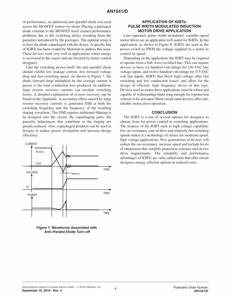
of performance, an optimized anti−parallel diode was usedacross the MOSFET source−to−drain. Placing a packageddiode external to the MOSFET itself created performanceproblems due to the switching delays resulting from theparasitics introduced by the packages. The optimal setup isto have the diode copackaged with the device. A specific lineof IGBTs has been created by Motorola to address this issue.These devices work very well in applications where energyis recovered to the source and are favored by motor controldesigners.
Like the switching device itself, the anti−parallel diodeshould exhibit low leakage current, low forward voltagedrop and fast switching speed. As shown in Figure 7, thediode forward drop multiplied by the average current itpasses is the total conduction loss produced. In addition,large reverse recovery currents can escalate switchinglosses. A detailed explanation of reverse recovery can befound in the Appendix. A secondary effect caused by largereverse recovery currents is generated EMI at both theswitching frequency and the frequency of the resultingringing waveform. This EMI requires additional filtering tobe designed into the circuit. By copackaging parts, theparasitic inductances that contribute to the ringing aregreatly reduced. Also, copackaged products can be used indesigns to reduce power dissipation and increase designefficiency.
Figure 7. Waveforms Associated with Anti−Parallel Diode Turn−off
IRM(rec)
TIME
TIME
TIME
POWER
VOLTAGE
CURRENT
IIGBT
IDIODE
Vf
APPLICATION OF IGBTs:PULSE WIDTH MODULATED INDUCTION
MOTOR DRIVE APPLICATIONLine−operated, pulse−width modulated, variable−speed
motor drives are an application well suited for IGBTs. In thisapplication, as shown in Figure 8, IGBTs are used as thepower switch to PWM the voltage supplied to a motor tocontrol its speed.
Depending on the application, the IGBT may be requiredto operate from a full−wave rectified line. This can requiredevices to have six hundred volt ratings for 230 VAC linevoltage inputs, and twelve hundred volt ratings for 575 VACvolt line inputs. IGBTs that block high voltage offer fastswitching and low conduction losses, and allow for thedesign of efficient, high frequency drives of this type.Devices used in motor drive applications must be robust andcapable of withstanding faults long enough for a protectionscheme to be activated. Short circuit rated devices offer safe,reliable motor drive operation.
CONCLUSIONThe IGBT is a one of several options for designers to
choose from for power control in switching applications.The features of the IGBT such as high voltage capability,low on−resistance, ease of drive and relatively fast switchingspeeds makes it a technology of choice for moderate speed,high voltage applications. New generations of devices willreduce the on−resistance, increase speed and include levelsof integration that simplify protection schemes and devicedrive requirements. The reliability and performanceadvantages of IGBTs are value added traits that offer circuitdesigners energy efficient options at reduced costs.
©Specifications subject to change without notice. 2016 Littelfuse, Inc.September 19, 2016 - Rev. 2
Publication Order Number:AN1541/D

AN1541/D
8
IGBT 1/2 BRIDGEIGBT
1/2 BRIDGE
Figure 8. Typical Pulse−Width, Modulated, Variable−Speed Induction Motor Drivesare Where IGBT’s Offer Performance Advantages
+230 VAC
TEMPERATURECONTROLSYSTEM
I/OLON®
CONTROL IC MCUOR ASIC
MIXED MODE ICCUSTOM LINEAR
ORSTANDARD CELL
GATE DRIVE HVICOR
OPTO & LVIC
DIODE BRIDGE
FILTERCAPACITOR
INDUCTIONMOTOR
IGBT1/2 BRIDGE
PHASE CURRENTS AND VOLTAGES
ACKNOWLEDGEMENTSThe writing of this document was assisted by a number of
internal device designers. Their assistance was greatlyappreciated by the authors. Bill Fragale, Steve Robb andVasudev Venkatesan provided device operation insight andreference materials. Graphic material was provided byBasam Almesfer and Steve Robb. Finally, C. S. Mitterassisted with editing and accuracy of the material.
REFERENCES1. D. Y. Chen, J. Yang, and J. Lee “Application of the
IGT/COMFET to Zero−Current SwitchingResonant Converters,” PESC, 1987.
2. B. J. Baliga, “Analysis of Insulated Gate TransistorTurn−off Characteristics,” IEEE Electron DeviceLett. EDL−6, (1985), pp. 74−77.
3. B. J. Baliga, “Switching Speed Enhancement inInsulated Gate Transistors by Electron Irradiation,”IEEE Transactions on Electron Devices, ED−31,(1984), pp. 1790−1795.
©Specifications subject to change without notice. 2016 Littelfuse, Inc.September 19, 2016 - Rev. 2
Publication Order Number:AN1541/D

AN1541/D
9
APPENDIXDiode Reverse Recovery Analysis [4]
Figure A−1. Reverse Recovery Waveform
total reverse recovery timefall time due to stored minority chargeapplication and device dependentpeak reverse recovery current
tb
ta
trr
IRM(rec)
IF
di/dt
Qa Qb
trr =ta =tb =IRM(rec) =
A typical reverse recovery waveform is shown inFigure A−1. The reverse recovery time trr has beentraditionally defined as the time from diode currentzero−crossing to where the current returns to within 10% ofthe peak recovery current IRM(rec). This does not giveenough information to fully characterize the waveformshape. A better way to characterize the rectifier reverserecovery is to partition the reverse recovery time into twodifferent regions, ta and tb, as shown in Figure A−1. The tatime is a function of the forward current and the applieddi/dt. A charge can be assigned to this region denoted Qa, thearea under the curve. The tb portion of the reverse recoverycurrent is not very well understood. Measured tb times varygreatly with the switch characteristic, circuit parasitics, loadinductance and the applied reverse voltage. A relativesoftness can be defined as the ratio of tb to ta. Generalpurpose rectifiers are very soft (softness factor of about 1.0),fast recovery diodes are fairly soft (softness factor of about0.5) and ultrafast rectifiers are very abrupt (softness factorof about 0.2).
[4] Source: “Motor Controls,” TMOS Power MOSFETTransistor Data, Q4/92, DL135, Rev 4, (Phoenix: Motorola,Inc., 1992), pp. 2−9−22 to 2−9−23.
©Specifications subject to change without notice. 2016 Littelfuse, Inc.September 19, 2016 - Rev. 2
Publication Order Number:AN1541/D

AN1541/D
10
Notes
©Specifications subject to change without notice. 2016 Littelfuse, Inc.September 19, 2016 - Rev. 2
Publication Order Number:AN1541/D

AN1541/D
11
Notes
©Specifications subject to change without notice. 2016 Littelfuse, Inc.September 19, 2016 - Rev. 2
Publication Order Number:AN1541/D

AN1541/D
12©Specifications subject to change without notice. 2016 Littelfuse, Inc.September 19, 2016 - Rev. 2
Publication Order Number:AN1541/D
Littelfuse products are not designed for, and shall not be used for, any purpose (including, without limitation, automotive, military, aerospace, medical, life-saving, life-sustaining, nuclear facility applications, devices intended for surgical implant into the body, or any other application in which the failure or lack of desired operation of the product may result in personal injury, death, or property damage) other than those expressly set forth in applicable Littelfuse product documentation. Warranties granted by Littelfuse shall be deemed void for products used for any purpose not expressly set forth in applicable Littelfuse documentation. Littelfuse shall not be liable for any claims or damages arising out of products used in applications not expressly intended by Littelfuse as set forth in applicable Littelfuse documentation. The sale and use of Littelfuse products is subject to Littelfuse Terms and Conditions of Sale, unless otherwise agreed by Littelfuse.
Littelfuse.com