AN1246: Techniques To Improve ZVS Full-bridge PerformanceTechniques to Improve ZVS...
14
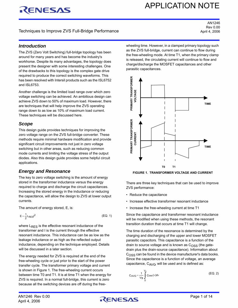
Techniques to Improve ZVS Full-Bridge Performance APPLICATION NOTE AN1246 Rev 0.00 Page 1 of 14 April 4, 2006 AN1246 Rev 0.00 April 4, 2006 Introduction The ZVS (Zero Volt Switching) full-bridge topology has been around for many years and has become the industry's workhorse. Despite its many advantages, the topology does present the designer with some interesting challenges. One of the drawbacks to this topology is the complex gate drive required to produce the correct switching waveforms. This has been resolved with Intersil products such as the ISL6752 and ISL6753. Another challenge is the limited load range over which zero voltage switching can be achieved. An ambitious design can achieve ZVS down to 50% of maximum load. However, there are techniques that will help improve the ZVS operating range down to as low as 10% of maximum load current. These techniques will be discussed here. Scope This design guide provides techniques for improving the zero voltage range on the ZVS full-bridge converter. These methods require minimal hardware modification and provide significant circuit improvements not just in zero voltage switching but in other areas, such as reducing common mode currents and limiting the voltage stress of the output diodes. Also this design guide provides some helpful circuit applications. Energy and Resonance The key to zero voltage switching is the amount of energy stored in the transformer inductance versus the energy required to charge and discharge the circuit capacitances. Increasing the stored energy in the inductance or reducing the capacitance, will allow the design to ZVS at lower output currents. The amount of energy stored, E, is: where L RES is the effective resonant inductance of the transformer and I is the current through the effective resonant inductance. This inductance can be as low as the leakage inductance or as high as the reflected output inductance, depending on the technique employed. Details will be discussed in a later section. The energy needed for ZVS is required at the end of the free-wheeling cycle or just prior to the start of the power transfer cycle. The transformer primary voltage and current is shown in Figure 1. The free-wheeling current occurs between time T0 and T1. It is at time T1 when the energy for ZVS is required. In a normal full-bridge, this current is zero because all the switching devices are off during the free- wheeling time. However, in a clamped primary topology such as the ZVS full-bridge, current can continue to flow during the free-wheeling mode. At time T1, when the primary clamp is released, the circulating current will continue to flow and charge/discharge the MOSFET capacitances and other parasitic capacitances. There are three key techniques that can be used to improve ZVS performance: • Reduce the capacitance • Increase effective transformer resonant inductance • Increase the free-wheeling current at time T1 Since the capacitance and transformer resonant inductance will be modified when using these methods, the resonant transition duration that occurs at time T1 will change. The time duration of the resonance is determined by the charging and discharging of the upper and lower MOSFET parasitic capacitors. This capacitance is a function of the drain to source voltage and is known as C OSS (the gate- drain plus the drain-source capacitance). Information about C OSS can be found in the device manufacturer's data books. Since the capacitance is a function of voltage, an average capacitance, C AVG , will be used and is defined as: 2 RES I L 2 1 E (EQ. 1) TIME PRIMARY TRANSFORMER VOLTAGE TIME PRIMARY TRANSFORMER CURRENT T0 T1 FIGURE 1. TRANSFORMER VOLTAGE AND CURRENT )d ( C V 1 C oss V 0 B AVG B (EQ. 2)
Transcript of AN1246: Techniques To Improve ZVS Full-bridge PerformanceTechniques to Improve ZVS...
Techniques to Improve ZVS Full-Bridge Performance
APPLICATION NOTE
AN1246Rev 0.00
April 4, 2006
IntroductionThe ZVS (Zero Volt Switching) full-bridge topology has been around for many years and has become the industry's workhorse. Despite its many advantages, the topology does present the designer with some interesting challenges. One of the drawbacks to this topology is the complex gate drive required to produce the correct switching waveforms. This has been resolved with Intersil products such as the ISL6752 and ISL6753.
Another challenge is the limited load range over which zero voltage switching can be achieved. An ambitious design can achieve ZVS down to 50% of maximum load. However, there are techniques that will help improve the ZVS operating range down to as low as 10% of maximum load current. These techniques will be discussed here.
ScopeThis design guide provides techniques for improving the zero voltage range on the ZVS full-bridge converter. These methods require minimal hardware modification and provide significant circuit improvements not just in zero voltage switching but in other areas, such as reducing common mode currents and limiting the voltage stress of the output diodes. Also this design guide provides some helpful circuit applications.
Energy and ResonanceThe key to zero voltage switching is the amount of energy stored in the transformer inductance versus the energy required to charge and discharge the circuit capacitances. Increasing the stored energy in the inductance or reducing the capacitance, will allow the design to ZVS at lower output currents.
The amount of energy stored, E, is:
where LRES is the effective resonant inductance of the transformer and I is the current through the effective resonant inductance. This inductance can be as low as the leakage inductance or as high as the reflected output inductance, depending on the technique employed. Details will be discussed in a later section.
The energy needed for ZVS is required at the end of the free-wheeling cycle or just prior to the start of the power transfer cycle. The transformer primary voltage and current is shown in Figure 1. The free-wheeling current occurs between time T0 and T1. It is at time T1 when the energy for ZVS is required. In a normal full-bridge, this current is zero because all the switching devices are off during the free-
wheeling time. However, in a clamped primary topology such as the ZVS full-bridge, current can continue to flow during the free-wheeling mode. At time T1, when the primary clamp is released, the circulating current will continue to flow and charge/discharge the MOSFET capacitances and other parasitic capacitances.
There are three key techniques that can be used to improve ZVS performance:
• Reduce the capacitance
• Increase effective transformer resonant inductance
• Increase the free-wheeling current at time T1
Since the capacitance and transformer resonant inductance will be modified when using these methods, the resonant transition duration that occurs at time T1 will change.
The time duration of the resonance is determined by the charging and discharging of the upper and lower MOSFET parasitic capacitors. This capacitance is a function of the drain to source voltage and is known as COSS (the gate-drain plus the drain-source capacitance). Information about COSS can be found in the device manufacturer's data books. Since the capacitance is a function of voltage, an average capacitance, CAVG, will be used and is defined as:
2RESIL
2
1E (EQ. 1)
TIME
PR
IMA
RY
TR
AN
SF
OR
ME
R
VO
LTA
GE
TIME
PR
IMA
RY
TR
AN
SF
OR
ME
R
CU
RR
EN
T
T0 T1
FIGURE 1. TRANSFORMER VOLTAGE AND CURRENT
)d(CV
1C oss
V
0B
AVG
B
(EQ. 2)
AN1246 Rev 0.00 Page 1 of 14April 4, 2006

Techniques to Improve ZVS
Full-Bridge Performance
where VB is defined as the supply voltage to the ZVS full-bridge converter. Since the upper and lower MOSFETs must charge and discharge, the total capacitance is twice CAVG. Therefore, the resonant frequency may be estimated by:
Because the MOSFET turns on after 1/4 of the cycle (/4 radians), the turn-on delay time is:
Equation 4 shows that if either the resonant inductance or capacitance of the MOSFETs increases, the resonant time will also increase. This delay reduces the range of usable duty cycle and must be taken into account in maximum duty cycle calculations. It is preferable to have a small resonant time.
In 400V designs, the resonant time is typically 300ns and in 48V units the time is 100ns. It is advisable to increase the inductance for energy storage and reduce the capacitance for resonant time and energy requirements.
Another reason for increasing the LRES/CAVG ratio is to improve the minimum load current to achieve ZVS operation. The amplitude of the resonant voltage on the transformer depends on the current in the inductance and the LC network’s characteristic impedance, which is the ratio of the inductance over MOSFET capacitance. This equates to:
where IPRI is the current through the transformer primary and VRES is the voltage across the transformer during the resonant time. As the primary current, IPRI, increases due to an increase in the load, the resonant voltage amplitude increases until it is clamped by the bulk voltage, VB. IPRI will then flow through the MOSFET's channel or body diode. Note that it is desirable to have the characteristic impedance value as large as possible so that low values of primary current will produce VRES > VB to achieve ZVS. For design purposes, the effective resonant inductance of the transformer should be high as possible, but not so high as to be detrimental to the resonant time, and the MOSFET capacitance should be kept to a minimum.
Note that by setting VRES equal to VB and solving for IPRI, the minimum reflected load current at which the converter will ZVS can be estimated.
Now that a basic understanding of the ZVS topology has been established, techniques for improving the performance can be discussed.
TransformerEvery time the voltage across the primary winding of the transformer changes, the transformer winding capacitance must be charged or discharged. Not only does this decrease
the available energy for ZVS but it is also a source of common mode currents which contribute to EMI emissions.
What can be done is to add more insulation tape between the primary and secondary windings. Doubling or tripling the insulation thickness will not increase the overall transformer size by much. By doing this, the leakage inductance is increased and the load current to maintain ZVS is lowered. The common mode currents may be decreased by 1/2 to 1/3, depending on the tape thickness.
Unlike other topologies, leakage inductance is beneficial in the ZVS full-bridge. Higher leakage energy results in more losses in the primary side snubbers in a standard full-bridge. The higher energy is desired in the ZVS full-bridge.
Arbitrarily increasing the leakage inductance may have detrimental effects as well. One concern is eddy currents in the transformer windings due to high H fields [1]. If the H fields get too high, the primary and secondary windings should to be interleaved to reduce AC winding losses.
Another transformer modification that can be done is to gap the transformer core. This decreases the magnetizing inductance and increases the magnetizing current, thereby increasing the energy stored. Even a small gap will improve the ZVS performance since the energy stored is proportional to I2. Gapping the core will help to improve ZVS slightly, and yield other benefits as well
• By gapping the core more than 2mils, the variation in magnetizing inductance from unit to unit can be significantly reduced. When putting 2 core halves together, a gap of anywhere from 0 to 2mils may be formed due to uneven mating surfaces.
• If the supply voltage to the converter is regulated, such as the output of a PFC, the core may be gapped to the obtain the correct magnetizing current for the desired slope compensation.
The draw back with gapping the core is the slight increase in primary current and conduction losses of the MOSFETs.
MOSFETsAnother opportunity to reduce capacitance is to use lower capacitance MOSFETs. It is often tempting to use low RDSON MOSFETs to minimize conduction losses. However, a low RDSON MOSFET will have high capacitances that will hurt the minimum load at which the converter will ZVS. Because of the high capacitance, switching loss can become an issue at light loads where ZVS does not occur.
Figure 2 shows such an example. MOSFET #1 is a low RDSON, high capacitance MOSFET. MOSFET #2 has twice the RDSON and half the capacitance, or ½ the die size. In this example, MOSFET #1 design will no longer ZVS below 5A. You will note that at 0A load, the MOSFET power loss is higher than the power loss at full load. This happens because the switching loss can be higher than the conduction loss. In
CL22
1=F
AVGRESRES
(EQ. 3)
2
CL2=
F4
1=T
AVGRES
RESDELAY
(EQ. 4)
C2L
I=VAVG
RESPRIRES
(EQ. 5)
AN1246 Rev 0.00 Page 2 of 14April 4, 2006
Techniques to Improve ZVS
Full-Bridge Performance
conventional full-bridge converters, the power loss curve is monotonic and higher in value because the power loss is always the sum of conduction + switching loss. This is not the case in ZVS full-bridges. In this example, a design with MOSFET #1 will dissipate 15W more than at no load than at full load.
MOSFET #2 has higher conduction losses at full load but lower switching loss at light loads. Also note that switching loss does not become an issue until the load current drops below 3A. The lower capacitance requires less energy to achieve ZVS. Even though the conduction loss is higher at 20W, it is less than the 25W maximum loss using MOSFET #1. When one considers maximum losses, it is apparent that a design using MOSFET #2 would yield superior thermal performance.
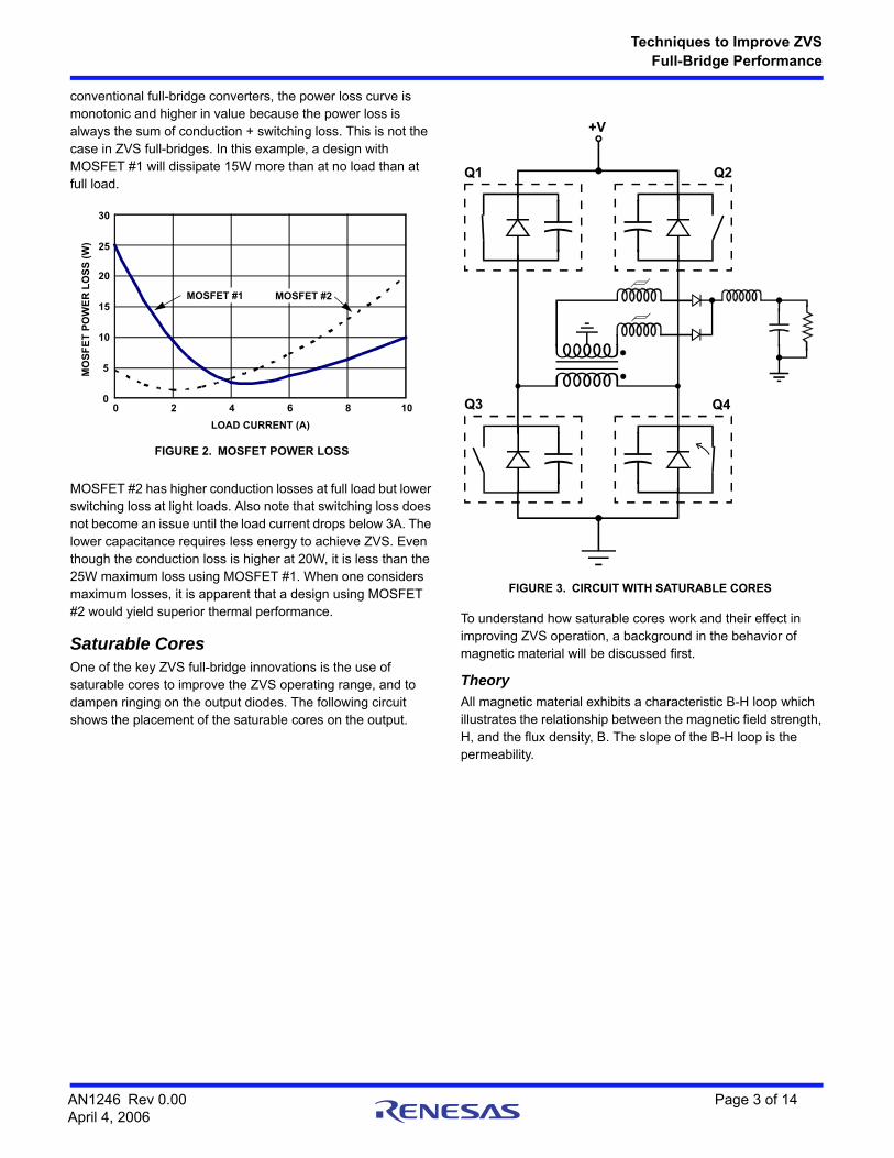
Saturable CoresOne of the key ZVS full-bridge innovations is the use of saturable cores to improve the ZVS operating range, and to dampen ringing on the output diodes. The following circuit shows the placement of the saturable cores on the output.
To understand how saturable cores work and their effect in improving ZVS operation, a background in the behavior of magnetic material will be discussed first.
Theory
All magnetic material exhibits a characteristic B-H loop which illustrates the relationship between the magnetic field strength, H, and the flux density, B. The slope of the B-H loop is the permeability.
0
5
10
15
20
25
30
0 2 4 6 8 10
LOAD CURRENT (A)
MO
SF
ET
PO
WE
R L
OS
S (
W)
MOSFET #1 MOSFET #2
FIGURE 2. MOSFET POWER LOSS
FIGURE 3. CIRCUIT WITH SATURABLE CORES
AN1246 Rev 0.00 Page 3 of 14April 4, 2006

Techniques to Improve ZVS
Full-Bridge Performance
When used in this application, the saturable core's B-H loop is typically operated in one quadrant, as shown below.
As the magnetic field strength, H, increases from zero, the flux density, B, increases until a saturation point occurs known as BSAT. When BSAT is reached the permeability of the material reduces to 0, the permeability of free space. BSAT occurs at HSAT. As H continues to increase, B increases at a much reduced rate, determined by 0. In this state the material is saturated.
Now, if H drops, B does not decrease significantly until H becomes slightly negative and then the core starts to reset. The value of H required to reset (demagnetize) the core is known as the coercivity or HC.
Based on this information, a simplification can be made. If H < HSAT, the permeability ( = B/H) is high and if H > HSAT, the permeability is low, as shown below:
Since inductance is directly related to permeability, the inductance also varies with H. However, the inductance also depends on the physical shape of the core and its magnetic
properties. Currently only toroidal shaped cores are used because of their ease in winding and lower cost. A drawing of a saturable core is shown in Figure 6.
There are a couple important core parameters to consider. One is lm, the mean magnetic path length of the core, and the other is the effective cross sectional area, Ae. The inductance for a toroidal shaped core is:
where (I) indicates that is a function of I. The core permeability has 2 states and because of this, the inductance has two states. The relationship between H and I is:
where I is the current and N is the number of turns. The current magnitude that saturates the core is then:
The permeability of the core with zero or low bias will have a high while at currents above ISAT, drops to o. The inductance as a function of current is illustrated in the figure below:
Figure 7 shows that when I < ISAT, the inductance is high and when I > ISAT, the inductance is near 0.
The core characteristics can now be used to understand core operation in a circuit. When a voltage is first applied to the core, the current ramps up. During this time the core is in a blocking state. It behaves as a high impedance or a very large
B
BSAT
HHSAT
FIGURE 4. B-H LOOP
HSAT H
FIGURE 5. PERMAEBILITY vs H
Im
Ae
FIGURE 6. SATURABLE CORE GEOMETRY
l
AN)I(=Lm
e2 (EQ. 6)
l
NI=H
m
(EQ. 7)
NlH=ImSAT
SAT (EQ. 8)
ISAT
L
0
FIGURE 7. INDUCTANCE vs ISAT
AN1246 Rev 0.00 Page 4 of 14April 4, 2006

Techniques to Improve ZVS
Full-Bridge Performance
inductor. When the current reaches ISAT, the inductance drops to approximately zero henries and the impedance becomes very low. If there are any other impedances in the circuit, the applied voltage will drop across these components and the voltage across the core drops to nearly zero volts. The following figure graphically shows this effect.
The saturable core acts as a high impedance (switch open) until the current has ramped up to ISAT. The period of time that the core remains in a high impedance state is known as the blocking time, tB. Also note, from Faraday’s Law, that magnetic cores have a constant volt-time characteristic. If the voltage applied to the core (VCORE) is increased, the blocking time decreases proportionally such that the volt-time product is always constant. The reason for this is that if VCORE increases, so does the rate of current rise so that less time is needed to reach ISAT.
The relationship between voltage, current and time is quite simple. For I < ISAT, the saturable core behaves like an inductor:
The applied voltage is known, dI is simply ISAT and dt is the blocking time, tB. Solving for tB results in:
Substituting L and ISAT:
Simplifying the equation:
This equation describes the blocking time as a function of the applied voltage (VCORE), the core geometry and turns (AeN), and the magnetic material property (HSAT). There are some interesting relationships revealed by Equation 12. First, the blocking time has nothing to do with the mean magnetic length, lm. For a given material, varying the number of turns or the area of the core affects the blocking capability. Different materials have different HSAT values. For example, J and W material from Magnetics Inc.[2] have the same HSAT value, yet R material is quite different. Equation 12 is an approximation, and as such, is more useful for exploring relative relationships. It was derived assuming a constant applied voltage when in fact the voltage waveform is more complex. Even though Equation 12 may not predict the exact blocking time, it will show what parameters to vary to change the blocking time.
The next issue requiring discussion is how the core gets reset. From the B-H loop for the materials being discussed, if H does not go negative to reset the core, the core will always be in a saturated state. The core reset is directly related to the reverse recovery characteristics of the rectifier used.
In the circuit, there is a small amount of reverse charge (or current) to reset the core when it's placed in series with the diode. This reverse current results from discharging the diode capacitance (Schottky) or junction charge during turn-off. This current resets the core to some point so that a minor loop can be formed. Assuming there is sufficient reverse current to equal -HC, the degree of reset depends on the voltage applied to the core winding and the duration for which it is applied. While the core is being reset, the reverse current must equal the value of current corresponding to -HC. This behavior softens the reverse recovery characteristics. It should be noted that HC is not a fixed value, but is dependent on the core permeability and the rate of change of the flux. The degree of core reset, therefore, depends on the stored charge in the diode junction.
It has been found that Magnetics Inc. W and J material offer excellent blocking characteristics. However, materials such as R or Metglas FT-3 and 2714A materials (Metglas, Inc./Hitachi) do not reset with typical Schottky diodes and thus stay in a saturated state. The reason for this is that the reverse current is not high enough or on long enough to fully reset the core because these cores have a higher HC than either W or J material. Therefore, the core does not form a minor loop. This effect has been seen when using Schottky, GaAs or SiC diodes. For PN diodes, the effect is quite different. These diodes have a high reverse recovery charge. This reverse recovery charge is directly proportional to the forward current at which the diode operates. As the forward current increases through the diode, the saturable core resets deeper and the B-
0
VCORE
t
ICORE
0
ISAT
tB
t
FIGURE 8. BLOCKING CHARACTERISTICS
dt
dIL=V (EQ. 9)
CORE
SATB V
IL=t
(EQ. 10)
N
lHx
l
ANxV
1=t mSAT
m
e2
COREB (EQ. 11)
SATeCORE
B HNAV
1t (EQ. 12)
AN1246 Rev 0.00 Page 5 of 14April 4, 2006

Techniques to Improve ZVS
Full-Bridge Performance
H loop increases. Of course, an increase in B-H loop area means increase in power dissipation. It also means that the blocking time increases with the forward current. Neither of these effects are desirable. It's not recommended that PN diodes be used with saturable cores unless they have very good reverse recovery characteristics.
For low voltage designs both tB and PCORE are proportional to the number of turns. However, at higher voltages an interesting phenomenon occurs. Core loss is also dependent on the diode used. Core loss is defined as:
where f is the switching frequency, B is defined as the change in flux density of the minor loop. The reset current determines how far the core resets. As reset current goes up, B increases. This has an effect on blocking, such as:
The reset current changes because the dv/dt applied to the diode changes due to the inductance of the core. So, as N increases, the inductance increases, the reset current decreases and so does B. Thus, with N going up and B going down, VCORE x tB (volt-time) is not easily predicted.
The following figure shows the results of experimentation with 48V output units.
It shows that changing turns in a certain region of operation will have little effect on blocking time but a major effect on core loss. This is something to consider for higher output voltage designs.
Behavior of Saturable Cores in Circuit
The saturable cores behave as switches in the ZVS full-bridge topology steering the secondary current to maximize the primary current during free-wheeling. In a standard full-bridge the output inductor current is split into each secondary winding during the free-wheeling time and there is no primary current. In the ZVS full-bridge the secondary will be directed to one side only. The following figures will step through each mode of operation to show how the saturable core behaves.
On Mode 1
For On Mode 1, known as the power transfer cycle
• Q1, Q4 is on
• Q2, Q3 is off
• L1 is reset (high impedance)
• L2 is saturated (short)
The current is flowing through the channels of Q1 and Q4. The transformer has the full supply voltage across it. Due to the secondary voltages, all the secondary current will flow through L2 and current is blocked by the series diode for L1.
0
2
0
core dt)B(1
fdtHBfP (EQ. 13)
BNAtV eBCORE (EQ. 14)
PC
OR
E
N
VO
LT-T
IME
N
FIGURE 9. CORE LOSS, BLOCKING TIME EFFECTS WITH NUMBER OF TURNS
L1
L2
+V
FIGURE 10. ON MODE 1
AN1246 Rev 0.00 Page 6 of 14April 4, 2006

Techniques to Improve ZVS
Full-Bridge Performance
Free-wheeling Mode
For the Free-wheeling Mode
• Q1 is on
• Q2, Q3, Q4 is off
• L1 is reset (high impedance)
• L2 is saturated (short)
The current is flowing through the channel of Q1 and the body diode of Q2. The transformer has approximately 0V across the primary winding. The secondary winding voltage is also at 0V, and the secondary side free-wheeling current continues to flow through L2. L2 is in a saturated state while L1 still remains in a reset state (high impedance). There is not enough voltage across L1 to ramp the current up and saturate the core. During this time, the primary side free-wheeling current will be the reflected output inductor current plus magnetizing current.
Resonant Mode
For the Resonant Mode
• Q2 is on
• Q1, Q3, Q4 is off
• L1 is blocking (high impedance)
• L2 is saturated (short)
The current continues to flow in the primary and secondary windings. The primary current charges the capacitance of Q1 and discharges the capacitance of Q3. At the node of Q1 and Q3, the voltage is decreasing and the voltage across the transformer is reversing polarity. The voltage is also reversing polarity on the secondary. As the voltage reverses, the voltage across L1 will increase and remain in a blocking state until saturated. During this time the output inductor current continues to flow through L2 and assists the ZVS transition.
As L1 saturates, the voltage across L1 decreases, a reverse voltage across the diode in series with L2 develops and the output inductor current transfers from L2 to L1. Just as the voltage across the diode in series with L2 reverses, the reverse recovery current from the diode resets L2. After which L2 is fully reset and L1 is saturated.
This is the key mode where the highest current in the primary is required to charge and discharge the capacitance for ZVS
L1
L2
+V +V
FIGURE 11. FREE-WHEELING MODE
L1
L2
?V +V
FIGURE 12. RESONANT MODE
AN1246 Rev 0.00 Page 7 of 14April 4, 2006
Techniques to Improve ZVS
Full-Bridge Performance
operation. The saturable cores help steer the current to achieve this by keeping the primary current as high as possible.
On Mode 2
For On Mode 2, the other power transfer cycle
• Q2, Q3 is on
• Q1, Q4 is off
• L1 is saturated (short)
• L2 is reset (high impedance)
The current is flowing through the channel of Q2 and Q3. If there is excess ZVS energy, as there will be for all loads that exceed the minimum load for which ZVS occurs, the primary current direction must be reversed before power transfer to the secondary can occur. The delay this introduces causes the reduction of effective duty cycle mentioned earlier. L1 has gone past its blocking state and is now saturated. L2 has now completely reset and is in a high impedance state.
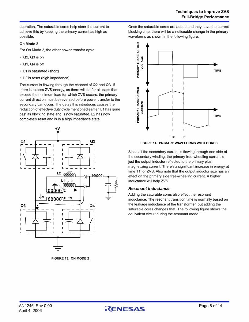
Once the saturable cores are added and they have the correct blocking time, there will be a noticeable change in the primary waveforms as shown in the following figure.
Since all the secondary current is flowing through one side of the secondary winding, the primary free-wheeling current is just the output inductor reflected to the primary plus magnetizing current. There's a significant increase in energy at time T1 for ZVS. Also note that the output inductor size has an effect on the primary side free-wheeling current. A higher inductance will help ZVS.
Resonant Inductance
Adding the saturable cores also effect the resonant inductance. The resonant transition time is normally based on the leakage inductance of the transformer, but adding the saturable cores changes that. The following figure shows the equivalent circuit during the resonant mode.
L1
L2
?V +V
FIGURE 13. ON MODE 2
TIME
PR
IMA
RY
TR
AN
SF
OR
ME
R
VO
LTA
GE
TIME
PR
IMA
RY
TR
AN
SF
OR
ME
R
CU
RR
EN
T
T0 T1
FIGURE 14. PRIMARY WAVEFORMS WITH CORES
AN1246 Rev 0.00 Page 8 of 14April 4, 2006

Techniques to Improve ZVS
Full-Bridge Performance
The circuit shows an ideal transformer with N:1 ratio. The leakage and magnetizing inductance are represented as discrete components on the primary side. The output section is a center tap with diodes, saturable cores and an output filter. During the resonant mode, one core is blocking and the other is in a saturated state. Most of the secondary transformer voltage will be across the saturable core in the blocking state. Both diodes are on except one will be conducting most of the current. With that in mind, both diodes and the saturated core can be redrawn as short circuits. This then simplifies to the circuit as indicated in the middle circuit of Figure 15. Further simplification can be made by reflecting all the circuit elements to the primary. Since the magnetizing inductance, LM is much greater than the leakage inductance LL (LM >> LL), the circuit can further simplify down to magnetizing inductance in parallel with the inductance of the saturable core in a blocking state reflected to the primary. Even further simplification can further be made if the reflected saturable core inductance is much greater than the magnetizing inductance. Now the magnetizing inductance LM, becomes the resonant inductance, LRES. This significantly increases the stored energy. It is not uncommon to achieve ZVS at 10% of maximum load using this technique with saturable cores.
The following equation describes the resonant inductance.
This shows that depending on the saturable core's inductance, the resonant inductances can vary from the leakage inductance to the magnetizing inductance of the transformer. Since the resonant inductance increased, there will be an effect on the resonant delay (increasing it), and the MOSFET timing must be adjusted accordingly. The increased delay will
also reduce the effective maximum duty cycle, but the added performance is well worth the trade off.
Output Diode Snubbers
If the proper saturable cores are chosen, RC snubbers are not required. The energy required to dampen the secondary can be found by taking advantage of the core loss of the saturable cores. Also, using the saturable cores as snubbers will produce a much cleaner reverse voltage waveform.
The saturable core model looks like an inductor in parallel with a resistor. This resistor emulates the core loss which helps to dampen the ringing from the output diode. The following figure shows an equivalent circuit.
VT represents the transformer secondary winding. LT is the secondary side leakage inductance. LC and RC represent the saturable core inductance, LC, and core loss, RC. CD is the output diode capacitance during reveres recovery. During reverse recovery the saturable core is coming out of saturation and the inductance is increasing. During that time, VT will be across the parallel network formed by LC and RC. The inductive impedance will be higher than RC so therefore RC will dominate and form an L-R-C circuit with LT and CT. This is much more effective as a snubber than placing an R-C network across the output diode.
The equivalent core loss resistance is a function of the core geometry, applied waveform, and core material. Core loss resistance is inversely proportional to core loss. Higher core loss results in a lower RC which also results in more dampening. The following equation shows an approximation to core loss.
where f is the switching frequency, VC is the voltage across the core and RK is a core loss resistance constant based on the material. If there is sufficient blocking capability, then VC and VT are approximately equal. Increasing either the switching frequency or the voltage across the core will increase the core loss, but modifying the core geometry will also have an effect. This equation is useful for solving problems with saturable cores that are running too hot. Note that while lm has no effect on the blocking time, it does affect the core loss.
BLOCKINGN : 1LL
LMLRES
SATURATED
LSAT
LSAT
N : 1LL
LMLRES LSAT
LL
LMLRES
LSATN2---- 2
LM LSATN2---- 2
FIGURE 15. RESONANT MODE EQUIVALENT CIRCUIT
L
2
SATM
RES L
2
NL
1+
L
11
=L
(EQ. 15)
+- VT
LT LC
RC
CD+VOUT
FIGURE 16. SNUBBER EQUIVALENT CIRCUIT
TRANSFORMERSATURABLE
CORE DIODE
K
SATm2CC
R
H
N
l)(VfP (EQ. 16)
AN1246 Rev 0.00 Page 9 of 14April 4, 2006

Techniques to Improve ZVS
Full-Bridge Performance
Choosing the Right Core
Now that the theory has been discussed, choosing the correct saturable core is next. This is only a guide in directing the user in the right direction in selecting saturable cores.
For output designs of 5V or less, start with a single turn W-material core, such as 40705 from Magnetics Inc. For higher output voltages, VCORE will be higher and requires more turns on the saturable core. For example, 48V output designs will need about 4 turns to maintain the same blocking performance. Also, core loss becomes an issue and F material is suggested as a starting point.
The blocking volt-time waveforms applied to the saturable cores are not simple. The voltage across the core is illustrated in Figure 17.
Figure 17 shows the blocking voltage of three different cores, each with a different blocking time. The shape of the blocking voltage waveform results from resonant ringing. Each of these traces shows different core blocking times.
• Curve A shows a core with not enough blocking. The peak voltage does not reach the same voltage as the reverse voltage on the output diode. To fix this problem either increase the core area or the number of turns. The affect on the primary is that the resonant time will be short and it will take a higher load current to ZVS.
• Curve B represents a core where the peak voltage is just about equal to the output diode reverse voltage. This is the optimal design. There is just enough blocking for the resonant period and not too much to affect the maximum duty cycle. When the primary D-S voltage on the MOSFET rings to 0 V, it has reached the point at which the blocking time is no longer needed.
• Curve C shows too much blocking. This is shown by the clipped voltage resulting from not enough transformer secondary voltage. This also drastically affects the maximum duty cycle of the output inductor and increases the core loss. For this situation, reduce the core area or the number of turns.
The "rule of thumb" when choosing a core is to set the blocking so that clipping just starts to occur. If there is insufficient blocking capability it will be more difficult to ZVS. If there is too much blocking, too much time will be taken to saturate the
core, and the effective duty cycle will be lowered. Additionally, there will be excessive core loss in the saturable cores.
Different materials will have different affects on blocking. W and J material from Magnetics Inc. have the exact same blocking characteristics. F, R and Metglas materials have a higher HC which requires higher reverse current to reset the core. They require an extra winding which carries current to offset the B-H loop for 5V output designs. See Figure 21. For 48V output designs, these materials do not require an extra winding but will require more turns than W material because the HSAT product is less.
The amount of damping required is dependent upon the user. A well damped design will require the saturable core to dissipate more energy than an under damped design. W and J material have the same blocking characteristics, but the core loss resistance is higher in J material. It does not dampen as well as the W material. F, R and Metglas materials usually do not dampen enough unless an extra winding for current is used as in Figure 21, or an extra resistor is used in parallel with the core. The parallel resistor decreases the overall core loss resistance and dissipates the power in another element.
Another effect to consider is the frequency of operation. Core loss is directly proportional to the frequency. The frequency limitation is around 150kHz for the ferrite materials (like W, J and R) and up to 200kHz for Metglas.
Thermal
One of the big issues with saturable cores is self-heating due to core loss. Depending on the material this could become a major issue.
All magnetic materials have what is known as the Curie temperature. If this temperature point is exceeded, the relative permeability, r, of the material reduces to 1, the same as free space. In actual designs this temperature should never be approached in a core. The Curie temperature varies significantly from one material to the next. For example, Magnetic Inc.'s F material has a Curie temperature of 250°C while W material is only 125°C.
There are varies ways to minimize the self heating of the saturable core. Keeping the blocking time as low as possible or keeping the switching frequency to the minimum. Another is to use materials that have low damping to the diode voltage ringing and use a parallel resistor. Increasing lm and keeping Ae constant will increase core loss and dampening on the diode. However, the improvement in cooling due to the increase in surface area to volume ratio outweighs the increase in core loss. These methods were discussed earlier. However, if these techniques are not practical and core temperature is still a problem, the following techniques can be applied to the core.
Reducing the heating from the wire can help reduce the overall temperature. Instead of one large wire, use multiple insulated wires in parallel where the radius of the wire is less than the
VC
OR
E
TIME
A B C
MAXIMUM
VOLTAGE
FIGURE 17. VARIOUS CORE BLOCKING TIMES
AN1246 Rev 0.00 Page 10 of 14April 4, 2006

Techniques to Improve ZVS
Full-Bridge Performance
skin depth at the operating frequency. Avoid bunching up the wire so that heating due to the wires do not generate a local hotspot. Having a short lead distance between the core winding and a large copper area on the PWB will help conduct the heat out of the core.
Placing the saturable core in high airflow also helps. However, careful core temperature measurements must be made to detect "dead spots" in the airflow. That part of the core can have high temperatures because of minimal airflow.
It is also possible to heatsink a saturable core. The following figure shows such a design.
Figure 18 shows a saturable core with 4 turns mounted on a metal plate acting as a heatsink. Between the core and heatsink is a thermally conductive adhesive or epoxy to make better thermal contact between the core, windings and metal plate. This method has been shown to be very effective in cooling saturable cores.
Some core materials can be allowed to run hot because of their high curie temperature. However, if the temperature exceeds 130°C, it may be necessary to redesign the assembly for a higher rated insulation class per the relevant safety agencies.
ConclusionThis design guide shows several techniques to improve the ZVS range of the ZVS full-bridge converter. Some like the transformer are easy to implement while the saturable cores offers other significant advantages. Also what is provided is some practical design considerations and guidelines with these techniques.
References[1] Lloyd H Dixon Jr., "Eddy Current Losses in Transformer Windings and Circuit Wiring", SEM600 Unitrode Seminar
[2] Magnetics Inc. Ferrite Cores catalog, 1999
AppendixThe following section shows some useful circuit configurations involving saturable cores.
HEATSINK
CORE
ADHESIVE
WIRE
FIGURE 18. SATURABLE CORE HEATSINK
AN1246 Rev 0.00 Page 11 of 14April 4, 2006

Techniques to Improve ZVS
Full-Bridge Performance
Constant Blocking Time
The problem with wide range input converters is that the blocking time increases as the input voltage decreases. This is solved with the following circuit. This circuit behaves similar to magnetic amplifiers, but instead of regulating the output voltage, the blocking time will be held nearly constant as the secondary transformer voltage decreases. The circuit functions by using D5, D4 and C1 as a peak detect circuit. R2 and R3 form a voltage divider between the output voltage and voltage at C1. As the transformer secondary voltage decreases, the gate-source voltage increases and Q1 draws more current. As more current is drawn, the saturable cores will block less. R1 is a current limit resistor and D3 limits current flow to one direction. (Note: This configuration will work with a center-tapped output.)
Be careful of reverse voltage stress on the output diodes. When the saturable cores are disabled, there is no damping and reverse voltage ringing on the output diodes may be significant.
Magnetic Amplifier Post Regulator
Below is a magnetic amplifier circuit that can be used with the ZVS full-bridge topology. Not only does this facilitate post regulation on an output winding, but helps to ZVS the converter at the same time. For this application, the best saturable core material to use is either Permalloy 80 (Magnetics Inc.) or Metglas 2714A alloy or equivalent. In order to control the output voltage with this material, blocking must occur over a wider range resulting in higher volt-times and increased core loss.
FIGURE 19. CONSTANT BLOCKING TIME CIRCUIT
ROUTCOUT
D1LSAT1
L1
L2
ZVSCON-
VERTER
D5 D4
C1R2
LSAT2
D2
R3D3
Q1
R1
FIGURE 20. MAG-AMP CIRCUIT
ZVSCON-
VERTER
L2NP
MAINOUTPUTSECTION
+
-V0 LOAD
N2
D2
D3
D4
MAG-AMPCONTROL
L1 D1 LOUT
R1 C1 V1 LOAD
IM
+
-
T1
N2
AN1246 Rev 0.00 Page 12 of 14April 4, 2006

Techniques to Improve ZVS
Full-Bridge Performance
B-H Loop Modifier
It was mentioned earlier that some magnetic materials which have high HC, such as Metglas, do not work properly as saturable cores for ZVS converters. The problem with these materials is that there is not enough reset current to reset the core. To fix this problem, a small amount of IM is added to the core thus shifting the B-H loop.
FIGURE 21. B-H LOOP MODIFIER CIRCUIT
ZVSCON-
VERTER
L2NP
N2
D2
L1 D1 LOUT
R1 C1 V1 LOAD
IM
N2 +
-
RBLEED
AN1246 Rev 0.00 Page 13 of 14April 4, 2006

http://www.renesas.comRefer to "http://www.renesas.com/" for the latest and detailed information.
Renesas Electronics America Inc.1001 Murphy Ranch Road, Milpitas, CA 95035, U.S.A.Tel: +1-408-432-8888, Fax: +1-408-434-5351Renesas Electronics Canada Limited9251 Yonge Street, Suite 8309 Richmond Hill, Ontario Canada L4C 9T3Tel: +1-905-237-2004Renesas Electronics Europe LimitedDukes Meadow, Millboard Road, Bourne End, Buckinghamshire, SL8 5FH, U.KTel: +44-1628-651-700, Fax: +44-1628-651-804Renesas Electronics Europe GmbHArcadiastrasse 10, 40472 Düsseldorf, Germany Tel: +49-211-6503-0, Fax: +49-211-6503-1327Renesas Electronics (China) Co., Ltd.Room 1709 Quantum Plaza, No.27 ZhichunLu, Haidian District, Beijing, 100191 P. R. ChinaTel: +86-10-8235-1155, Fax: +86-10-8235-7679Renesas Electronics (Shanghai) Co., Ltd.Unit 301, Tower A, Central Towers, 555 Langao Road, Putuo District, Shanghai, 200333 P. R. China Tel: +86-21-2226-0888, Fax: +86-21-2226-0999Renesas Electronics Hong Kong LimitedUnit 1601-1611, 16/F., Tower 2, Grand Century Place, 193 Prince Edward Road West, Mongkok, Kowloon, Hong KongTel: +852-2265-6688, Fax: +852 2886-9022Renesas Electronics Taiwan Co., Ltd.13F, No. 363, Fu Shing North Road, Taipei 10543, TaiwanTel: +886-2-8175-9600, Fax: +886 2-8175-9670Renesas Electronics Singapore Pte. Ltd.80 Bendemeer Road, Unit #06-02 Hyflux Innovation Centre, Singapore 339949Tel: +65-6213-0200, Fax: +65-6213-0300Renesas Electronics Malaysia Sdn.Bhd.Unit 1207, Block B, Menara Amcorp, Amcorp Trade Centre, No. 18, Jln Persiaran Barat, 46050 Petaling Jaya, Selangor Darul Ehsan, MalaysiaTel: +60-3-7955-9390, Fax: +60-3-7955-9510Renesas Electronics India Pvt. Ltd.No.777C, 100 Feet Road, HAL 2nd Stage, Indiranagar, Bangalore 560 038, IndiaTel: +91-80-67208700, Fax: +91-80-67208777Renesas Electronics Korea Co., Ltd.17F, KAMCO Yangjae Tower, 262, Gangnam-daero, Gangnam-gu, Seoul, 06265 KoreaTel: +82-2-558-3737, Fax: +82-2-558-5338
SALES OFFICES
© 2018 Renesas Electronics Corporation. All rights reserved.Colophon 7.0
(Rev.4.0-1 November 2017)
Notice
1. Descriptions of circuits, software and other related information in this document are provided only to illustrate the operation of semiconductor products and application examples. You are fully responsible for
the incorporation or any other use of the circuits, software, and information in the design of your product or system. Renesas Electronics disclaims any and all liability for any losses and damages incurred by
you or third parties arising from the use of these circuits, software, or information.
2. Renesas Electronics hereby expressly disclaims any warranties against and liability for infringement or any other claims involving patents, copyrights, or other intellectual property rights of third parties, by or
arising from the use of Renesas Electronics products or technical information described in this document, including but not limited to, the product data, drawings, charts, programs, algorithms, and application
examples.
3. No license, express, implied or otherwise, is granted hereby under any patents, copyrights or other intellectual property rights of Renesas Electronics or others.
4. You shall not alter, modify, copy, or reverse engineer any Renesas Electronics product, whether in whole or in part. Renesas Electronics disclaims any and all liability for any losses or damages incurred by
you or third parties arising from such alteration, modification, copying or reverse engineering.
5. Renesas Electronics products are classified according to the following two quality grades: “Standard” and “High Quality”. The intended applications for each Renesas Electronics product depends on the
product’s quality grade, as indicated below.
"Standard": Computers; office equipment; communications equipment; test and measurement equipment; audio and visual equipment; home electronic appliances; machine tools; personal electronic
equipment; industrial robots; etc.
"High Quality": Transportation equipment (automobiles, trains, ships, etc.); traffic control (traffic lights); large-scale communication equipment; key financial terminal systems; safety control equipment; etc.
Unless expressly designated as a high reliability product or a product for harsh environments in a Renesas Electronics data sheet or other Renesas Electronics document, Renesas Electronics products are
not intended or authorized for use in products or systems that may pose a direct threat to human life or bodily injury (artificial life support devices or systems; surgical implantations; etc.), or may cause
serious property damage (space system; undersea repeaters; nuclear power control systems; aircraft control systems; key plant systems; military equipment; etc.). Renesas Electronics disclaims any and all
liability for any damages or losses incurred by you or any third parties arising from the use of any Renesas Electronics product that is inconsistent with any Renesas Electronics data sheet, user’s manual or
other Renesas Electronics document.
6. When using Renesas Electronics products, refer to the latest product information (data sheets, user’s manuals, application notes, “General Notes for Handling and Using Semiconductor Devices” in the
reliability handbook, etc.), and ensure that usage conditions are within the ranges specified by Renesas Electronics with respect to maximum ratings, operating power supply voltage range, heat dissipation
characteristics, installation, etc. Renesas Electronics disclaims any and all liability for any malfunctions, failure or accident arising out of the use of Renesas Electronics products outside of such specified
ranges.
7. Although Renesas Electronics endeavors to improve the quality and reliability of Renesas Electronics products, semiconductor products have specific characteristics, such as the occurrence of failure at a
certain rate and malfunctions under certain use conditions. Unless designated as a high reliability product or a product for harsh environments in a Renesas Electronics data sheet or other Renesas
Electronics document, Renesas Electronics products are not subject to radiation resistance design. You are responsible for implementing safety measures to guard against the possibility of bodily injury, injury
or damage caused by fire, and/or danger to the public in the event of a failure or malfunction of Renesas Electronics products, such as safety design for hardware and software, including but not limited to
redundancy, fire control and malfunction prevention, appropriate treatment for aging degradation or any other appropriate measures. Because the evaluation of microcomputer software alone is very difficult
and impractical, you are responsible for evaluating the safety of the final products or systems manufactured by you.
8. Please contact a Renesas Electronics sales office for details as to environmental matters such as the environmental compatibility of each Renesas Electronics product. You are responsible for carefully and
sufficiently investigating applicable laws and regulations that regulate the inclusion or use of controlled substances, including without limitation, the EU RoHS Directive, and using Renesas Electronics
products in compliance with all these applicable laws and regulations. Renesas Electronics disclaims any and all liability for damages or losses occurring as a result of your noncompliance with applicable
laws and regulations.
9. Renesas Electronics products and technologies shall not be used for or incorporated into any products or systems whose manufacture, use, or sale is prohibited under any applicable domestic or foreign laws
or regulations. You shall comply with any applicable export control laws and regulations promulgated and administered by the governments of any countries asserting jurisdiction over the parties or
transactions.
10. It is the responsibility of the buyer or distributor of Renesas Electronics products, or any other party who distributes, disposes of, or otherwise sells or transfers the product to a third party, to notify such third
party in advance of the contents and conditions set forth in this document.
11. This document shall not be reprinted, reproduced or duplicated in any form, in whole or in part, without prior written consent of Renesas Electronics.
12. Please contact a Renesas Electronics sales office if you have any questions regarding the information contained in this document or Renesas Electronics products.
(Note 1) “Renesas Electronics” as used in this document means Renesas Electronics Corporation and also includes its directly or indirectly controlled subsidiaries.
(Note 2) “Renesas Electronics product(s)” means any product developed or manufactured by or for Renesas Electronics.


![DC to DC Converter Using ZVS [Compatibility Mode]](https://static.fdocuments.us/doc/165x107/577d1d201a28ab4e1e8ba955/dc-to-dc-converter-using-zvs-compatibility-mode.jpg)