AN1161: ISL6421A Single LNB Controller with I2C Interface ... · 4.0GHz to 8.0GHz, while the Ku...
14
ISL6421A Single LNB Controller with I 2 C Interface for Advanced Satellite Set-Top Box Designs APPLICATION NOTE AN1161 Rev 2.00 Page 1 of 14 Jan 2, 2007 AN1161 Rev 2.00 Jan 2, 2007 Introduction Communication Satellite Frequency Allocation Communication satellites operate within two frequency bands for TV/Broadband service broadcast signals, C Band and Ku Band. The C Band overall frequency spectrum is 4.0GHz to 8.0GHz, while the Ku Band overall frequency spectrum is 11.7GHz to 18.0GHz. Within these bands, each satellite will have specific uplink and downlink frequency allocation. For example, the North American DBS system has categories assigned as follows: Ku Band high power downlink is 12.2GHz to12.7GHz and 17.3GHz to 17.8GHz as the uplink frequency, C Band downlink frequency is 3.7GHz to 4.2GHz and 5.925GHz to 6.425GHz as uplink frequency. Also, to use the frequencies that are available for satellite broadcast as efficiently as possible, and to accommodate an additional number of channels within a given frequency band, the transmission signal can be formatted to be either vertical and horizontal, or circular right-hand and circular left- hand simultaneously per frequency. What is a Low Noise Block (LNB)? An LNB is a low noise block module, placed on the focus of the dish antenna (parabola) that provides the following functions: • Down conversion of the incoming signal from GHz range to the 910MHz to 2150MHz (for Europe) range called “first conversion signal.” This conversion allows the signal to be carried by an inexpensive coaxial cable towards the receiver. • Signal amplification with good noise figure. The LNB improves the first conversion signal level through the use of a built-in low noise amplifier. • Selection of Vertical or Horizontal polarization. • Selects operating band by switching its internal oscillator from Low band to High band when the LNB “receives” a 22kHz tone. Specifically, the local oscillator (LO) frequency changes from 9.75GHz to 10.6GHz. C Band - LO frequency 9.75GHz Ku Band - LO frequency 10.6GHz • Miscellaneous functions based on 22kHz tone PPM encoding, as discussed later in this paper. Polarization Selection Polarization is a way to give a transmission signal specific direction. It increases the beam concentration. The signal transmitted by satellite can be polarized in one of four different ways: Linear (horizontal or vertical) or Circular (right-hand or left-hand). Consequently, the satellite can broadcast both H and V or LH and RH polarized signals on one frequency. The “universal” LNB switches the polarization by looking at the voltage that it receives from the receiver. 12V - Horizontal, 18V - Vertical 13V - Circular right-hand, 20V - Circular left-hand Generally, only two (12V and 18V or 13V and 20V) will be used with one type of antenna. Also, 1V can be added from a receiver to any of above voltages to compensate for the voltage drop in the coaxial cable, i.e., it could be 13V (12V), 14V (13V), 19V (18V) or 21V (20V) instead. 22kHz Tone and DiSEqC™ (Digital Satellite Equipment Control) Encoding In addition to selecting the polarization, the LNB needs to select the operating band. This is done with the use of a 22kHz tone frequency. A 22kHz pulse-position modulated signal of about 0.6V amplitude is superimposed on the LNB’s DC power rail. Its coding scheme allows the remote electronics to perform more complex functions like varying the down conversion frequency to select one of multiple LNB’s for dual-dish systems or physically rotating the antenna assembly. Traditionally, when other encoding functions do not require using 22kHz tone, simple presence or absence of this tone selects the operating band by changing the local oscillator frequency of the LNB. The complex encoding of the 22kHz burst is done with a more sophisticated communication bus protocol named the DiSEqC standard (Digital Satellite Equipment Control). The open DiSEqC standard developed by the European Telecommunication Satellite Organization is a well accepted worldwide standard for communication between satellite receivers and satellite peripheral equipment. The 22kHz oscillator has to be a tone generator with specific rise and fall time. The wave shape will be a quasi-square wave. (Sine with flat-top). The required frequency tolerance is ±2kHz over line and temperature variations. Burst coding of this signal is accomplished by input from the microcontroller at the DSQIN pin of the IC or by setting the ENT bit of the system register through the I 2 C bus as detailed in the ISL6421A datasheet. 22kHz WAVE SHAPE AND DETAILS (See Figures 1 and 2) Carrier frequency: 22kHz ±2kHz over line and temperature Carrier amplitude: 650mVpp ±250mV Modulation mark period: 500µs ±100µs Modulation space period: 1ms ±200µs
Transcript of AN1161: ISL6421A Single LNB Controller with I2C Interface ... · 4.0GHz to 8.0GHz, while the Ku...

ISL6421A Single LNB ConBox Designs
AN1161 Rev 2.00Jan 2, 2007
APPLICATION NOTE
AN1161
troller with I2C Interface for Advanced Satellite Set-Top Rev 2.00
Jan 2, 2007
Introduction
Communication Satellite Frequency Allocation
Communication satellites operate within two frequency bands for TV/Broadband service broadcast signals, C Band and Ku Band. The C Band overall frequency spectrum is 4.0GHz to 8.0GHz, while the Ku Band overall frequency spectrum is 11.7GHz to 18.0GHz.
Within these bands, each satellite will have specific uplink and downlink frequency allocation. For example, the North American DBS system has categories assigned as follows: Ku Band high power downlink is 12.2GHz to12.7GHz and 17.3GHz to 17.8GHz as the uplink frequency, C Band downlink frequency is 3.7GHz to 4.2GHz and 5.925GHz to 6.425GHz as uplink frequency.
Also, to use the frequencies that are available for satellite broadcast as efficiently as possible, and to accommodate an additional number of channels within a given frequency band, the transmission signal can be formatted to be either vertical and horizontal, or circular right-hand and circular left- hand simultaneously per frequency.
What is a Low Noise Block (LNB)?
An LNB is a low noise block module, placed on the focus of the dish antenna (parabola) that provides the following functions:
• Down conversion of the incoming signal from GHz range to the 910MHz to 2150MHz (for Europe) range called “first conversion signal.” This conversion allows the signal to be carried by an inexpensive coaxial cable towards the receiver.
• Signal amplification with good noise figure. The LNB improves the first conversion signal level through the use of a built-in low noise amplifier.
• Selection of Vertical or Horizontal polarization.
• Selects operating band by switching its internal oscillator from Low band to High band when the LNB “receives” a 22kHz tone. Specifically, the local oscillator (LO) frequency changes from 9.75GHz to 10.6GHz.C Band - LO frequency 9.75GHzKu Band - LO frequency 10.6GHz
• Miscellaneous functions based on 22kHz tone PPM encoding, as discussed later in this paper.
Polarization Selection
Polarization is a way to give a transmission signal specific direction. It increases the beam concentration. The signal transmitted by satellite can be polarized in one of four different ways: Linear (horizontal or vertical) or Circular (right-hand or left-hand). Consequently, the satellite can broadcast both H and V or LH and RH polarized signals on one frequency.
The “universal” LNB switches the polarization by looking at the voltage that it receives from the receiver.12V - Horizontal, 18V - Vertical13V - Circular right-hand, 20V - Circular left-hand
Generally, only two (12V and 18V or 13V and 20V) will be used with one type of antenna. Also, 1V can be added from a receiver to any of above voltages to compensate for the voltage drop in the coaxial cable, i.e., it could be 13V (12V), 14V (13V), 19V (18V) or 21V (20V) instead.
22kHz Tone and DiSEqC™ (Digital Satellite Equipment Control) Encoding
In addition to selecting the polarization, the LNB needs to select the operating band. This is done with the use of a 22kHz tone frequency. A 22kHz pulse-position modulated signal of about 0.6V amplitude is superimposed on the LNB’s DC power rail. Its coding scheme allows the remote electronics to perform more complex functions like varying the down conversion frequency to select one of multiple LNB’s for dual-dish systems or physically rotating the antenna assembly. Traditionally, when other encoding functions do not require using 22kHz tone, simple presence or absence of this tone selects the operating band by changing the local oscillator frequency of the LNB.
The complex encoding of the 22kHz burst is done with a more sophisticated communication bus protocol named the DiSEqC standard (Digital Satellite Equipment Control). The open DiSEqC standard developed by the European Telecommunication Satellite Organization is a well accepted worldwide standard for communication between satellite receivers and satellite peripheral equipment.
The 22kHz oscillator has to be a tone generator with specific rise and fall time. The wave shape will be a quasi-square wave. (Sine with flat-top). The required frequency tolerance is ±2kHz over line and temperature variations. Burst coding of this signal is accomplished by input from the microcontroller at the DSQIN pin of the IC or by setting the ENT bit of the system register through the I2C bus as detailed in the ISL6421A datasheet.
22kHz WAVE SHAPE AND DETAILS (See Figures 1 and 2)
Carrier frequency: 22kHz ±2kHz over line and temperatureCarrier amplitude: 650mVpp ±250mVModulation mark period: 500µs ±100µsModulation space period: 1ms ±200µs
Page 1 of 14

ISL6421A Single LNB Controller with I2CInterface for Advanced Satellite Set-Top Box
Methods of Modulation
ISL6421A - Provides a Complete Power Solution for LNB ControlThe ISL6421A is a highly integrated solution for supplying power and control signals from advanced satellite set-top box (STB) modules to the low noise block (LNB) of the antenna port. The device is comprised of a current-mode boost PWM and a low-noise linear regulator along with the circuitry required for I2C device interfacing and for providing DiSEqC standard control signals to the LNB.
The regulator output voltage is available at the output terminal (VOUT) to support operation of the antenna port in advanced satellite STBs. The regulator output for the PWM is set to 13V or 18V by a voltage select command (VSEL) through the I2C bus. Additionally, to compensate for the voltage drop in the coaxial cable, the selected voltage may be increased by 1V with the line length compensation (LLC) feature. An enable command sent on the I2C bus provides standby mode control for the PWM and linear combination, disabling the output to conserve power.
The current-mode boost converter provides the linear regulator with input voltage that is set to the output voltage, plus typically 1.2V dropout to insure minimum power dissipation across the linear regulator. This maintains constant voltage drop across the linear pass element while permitting adequate voltage range for tone injection.
Please refer to the ISL6421A datasheet, FN9130, for more information.
Quick Start Evaluation
Out Of The Box
The ISL6421A evaluation board is shipped in a “ready-to-test” state. The board requires an input voltage ranging from 8V to 14V and a 3.3V/5V supply. The use of an electronic load enables evaluation over a wide range of operating conditions. The evaluation kit ISL6405I2C-KIT-EVAL includes a PC to I2C bus interface board (USB-I2CIO), PC to I2C bus software, a USB cable, and a connector cable to connect the USB-I2CIO board and the ISL6421AEVAL1Z board, along with relevant application notes.
Required Test Equipment
To fully test the ISL6421A functionality, the following equipment is needed:
• 4 channel oscilloscope with probes
• 1 electronic load
• 2 bench power supplies
• Precision digital multi-meters
• I2C bus read/write capability
Power and Load Connections
The ISL6421A evaluation board has three sets of terminal posts used to supply the input voltages and to monitor and load the outputs.
Jumper Settings - JP1, JP2, and JP3 will be shorted with shunt jumpers pulling the ADDR, SEL18V, and the DISQIN pins low.
Input Voltage - Adjust two power supplies to provide the 5V/3.3V and 12V input voltages of the evaluation board. With the power supplies turned off, connect the positive lead of the 12V supply to the VIN post (P1) and the ground lead to the GND post (P2).
The second supply set for either 5V or 3.3V provides the pull-up voltage for the I2C bus clock and data line. Connect the positive lead of the second supply to the +5V/+3.3V post (P7) and the ground lead to the SGND post (P8).
FIGURE 1. DiSEqC™ MODULATION SCHEME
‘0’ DATA BIT ‘1’ DATA BIT
1.0ms 0.5ms 0.5ms 1.0ms
‘0’ TONE BURST (SATELLITE A)
‘1’ DATA BURST (SATELLITE B)
12.5ms
FIGURE 2. TIMING DIAGRAM FOR TONE BURST CONTROL SIGNAL
TABLE 1. ISL6421A EVALUATION BOARDS
BOARD NAME IC PACKAGE
ISL6421AEVAL1Z ISL6421AER 32 Ld QFN
AN1161 Rev 2.00 Page 2 of 14Jan 2, 2007

ISL6421A Single LNB Controller with I2CInterface for Advanced Satellite Set-Top Box
Output Voltage Loading and Monitoring - To exercise and monitor VOUT, connect the positive lead of one of the electronic loads and the positive lead of a digital multimeter to the VOUT post (P3) and the ground lead to the GND post (P4).
I2C Bus Communication Setup
To control and exercise the ISL6421A requires communication through the I2C bus clock (SCL) and data (SDA) pins. Refer to the ISL6421A datasheet for more information about the I2C bus specification. You can use existing I2C hardware/software, a word generator, or use the PC to I2C hardware/software included in the ISL6421A evaluation kit to produce the necessary I2C waveforms.
USB-I2CIO board driver installation - To use a PC to control the I2C bus to communicate with the ISL6421A you will have to install the drivers of the USB-I2CIO board included in the kit. You will need a Windows 98/XP/2000 machine with a standard USB port.
1. The evaluation kit comes with a CD containing the software and drivers to control the I2C bus. Copy the contents of the CD to some directory, e.g., C:\’some directory’.
2. Applying power to the USB-I2CIO board: The USB-I2CIO board has the option of being powered with 3.3V through the USB bus of the PC or externally with 5V connected to the +5 test point and GND test point. The I2C bus can operate at 3.3V or 5V logic levels. If you use an external 5V supply then place a shunt jumper shorting pins 2 and 3 of JP3. If you are using an external 5V supply to power the USB-I2CIO board, place a shunt jumper shorting pins 1 and 2 of JP3.
3. After the USB-I2CIO board is powered up, connect the USB cable to the USB port of a PC.
4. Windows should detect the new USB device and the ‘Found New Hardware Wizard’ should begin. This will help you install the drivers. Follow the directions on the screen until it asks you where to search for the drivers. At this point, you should select the ‘choose location’ option and browse to the C:\’some directory’ created in step one and select the drivers folder.
5. Follow the remaining directions and the driver should be installed and the USB-I2CIO detected by your PC.
6. If this is successful, another ‘Found New Hardware Wizard’ window will appear. Repeat steps 4 and 5. At this point, the USB-I2CIO board should be ready to use.
7. To connect the USB-I2CIO board to the ISL6421A evaluation board, use the 5 lead to 4 lead connector cable. Connect the 5 lead connector to J4 on the USB-I2CIO board and the 4 lead connector to J1 on the ISL6421A evaluation board.
8. Turn on the power supplies to power up the ISL6421A evaluation board.
9. Run the ISL6421A_I2C.exe program copied to C:\’some directory’. Figure 3 shows the PC to I2C software application window. Click the ‘Open Device’ button.
10. If you receive a ‘No USB Device Detected’ error:
• Make sure the drivers were installed correctly. If Windows did not detect your USB device, try running the Add/Remove Hardware Wizard in the control panel.
• Make sure the USB board is powered up (internally or externally, not both).
11. If you receive the ‘Incorrect Return Value’ error:
• The ISL6421A evaluation board may not be powered up. Check the power connections.
• Make sure SCL and SDA are connected correctly. The 5-pin connector to the USB-I2CIO board only fits one way. Try reversing the 4 lead connector at J1 of the ISL6421A evaluation board.
Using the PC to I2C Application
After opening the application window and clicking on the ‘Open Device’ button, the program will detect the USB-I2CIO board and initialize the I2C system registers of the ISL6421A. To evaluate the ISL6421A functionality, toggle the system register bits as needed and then click on the ‘Write I2C’ button to write to the system registers. The lower portion of the application window shows the current values of the system register bits. They are read and updated continuously. The OLF1 and OTF flag in system register 1 and 2 are read only bits and provide diagnostic status of the ISL6421A.
FIGURE 3. PC TO I2C APPLICATION WINDOW
AN1161 Rev 2.00 Page 3 of 14Jan 2, 2007

ISL6421A Single LNB Controller with I2CInterface for Advanced Satellite Set-Top Box
Performance Characterization
Startup
The ISL6421A features internal soft-start to reduce the external number of components. Figure 4 shows a typical soft-start waveform. Typical soft-start time is 4.6ms.
Shutdown
The LNB output of the ISL6421A can be shut down using the EN bit via I2C. Figure 5 shows a typical shutdown waveform.
Boost PWM Efficiency
The Boost PWM architecture allows close to 90% efficiency at full load as shown in Figure 6.
DiSEqC Implementation
The ISL6421A has a built-in 22kHz tone generator that can be controlled either by the I2C interface or by a dedicated pin (DSQIN) that allows immediate DiSEqC data encoding for the DiSEqC compliance. When the I2C tone enable bit (ENT) is set to HIGH, a continuous 22kHz tone is generated regardless of the status of the DSQIN pin. The ENT pin must be LOW when DSQIN pin is being used for DiSEqC encoding. Figure 7 shows the 22kHz tone waveform with 450mA load.
VOUT5V/DIV
FIGURE 4. SOFT-START
FIGURE 5. SHUTDOWN USING I2C ENABLE
VO15V/DIV
100µs/DIV
FIGURE 6. BOOST PWM EFFICIENCY vs LOAD
100
95
90
85
80
75
70
65
6050 150 250 350 450 550 650 750
IOUT (mA)
EF
FIC
IEN
CY
(%
)
22kHzTONE
tRISE = 8µstFALL = 7.4µs
20µs/DIV
FIGURE 7. 22kHz TONE OPERATION
200mV/DIV
AN1161 Rev 2.00 Page 4 of 14Jan 2, 2007
ISL6421A Single LNB Controller with I2CInterface for Advanced Satellite Set-Top Box
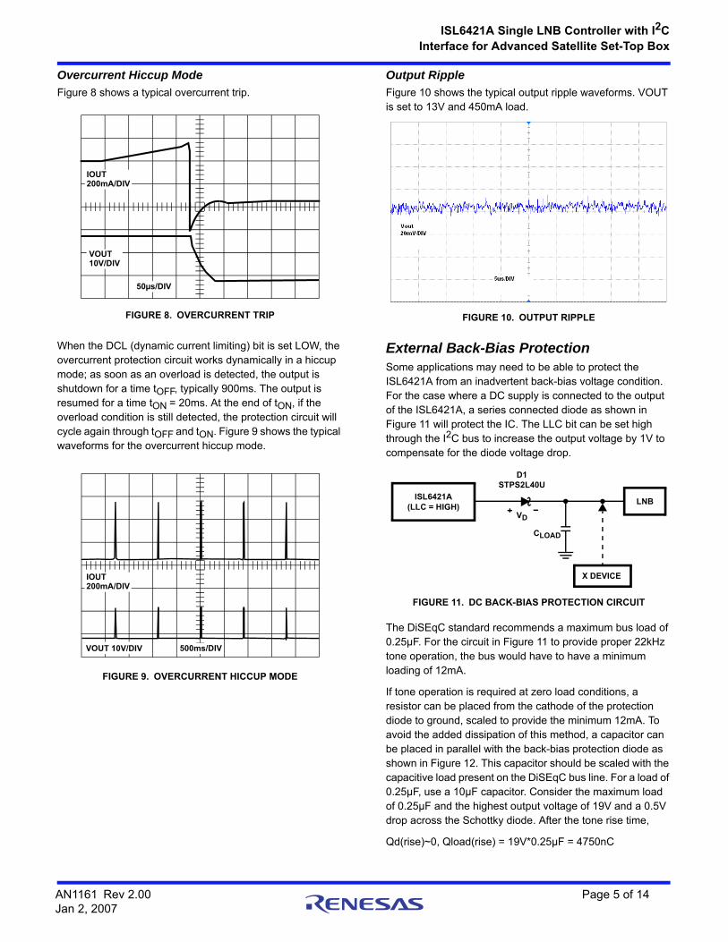
Overcurrent Hiccup Mode
Figure 8 shows a typical overcurrent trip.
When the DCL (dynamic current limiting) bit is set LOW, the overcurrent protection circuit works dynamically in a hiccup mode; as soon as an overload is detected, the output is shutdown for a time tOFF, typically 900ms. The output is resumed for a time tON = 20ms. At the end of tON, if the overload condition is still detected, the protection circuit will cycle again through tOFF and tON. Figure 9 shows the typical waveforms for the overcurrent hiccup mode.
Output Ripple
Figure 10 shows the typical output ripple waveforms. VOUT is set to 13V and 450mA load.
External Back-Bias ProtectionSome applications may need to be able to protect the ISL6421A from an inadvertent back-bias voltage condition. For the case where a DC supply is connected to the output of the ISL6421A, a series connected diode as shown in Figure 11 will protect the IC. The LLC bit can be set high through the I2C bus to increase the output voltage by 1V to compensate for the diode voltage drop.
The DiSEqC standard recommends a maximum bus load of 0.25µF. For the circuit in Figure 11 to provide proper 22kHz tone operation, the bus would have to have a minimum loading of 12mA.
If tone operation is required at zero load conditions, a resistor can be placed from the cathode of the protection diode to ground, scaled to provide the minimum 12mA. To avoid the added dissipation of this method, a capacitor can be placed in parallel with the back-bias protection diode as shown in Figure 12. This capacitor should be scaled with the capacitive load present on the DiSEqC bus line. For a load of 0.25µF, use a 10µF capacitor. Consider the maximum load of 0.25µF and the highest output voltage of 19V and a 0.5V drop across the Schottky diode. After the tone rise time,
Qd(rise)~0, Qload(rise) = 19V*0.25µF = 4750nC
FIGURE 8. OVERCURRENT TRIP
VOUT10V/DIV
IOUT200mA/DIV
50µs/DIV
VOUT 10V/DIV
IOUT200mA/DIV
500ms/DIV
FIGURE 9. OVERCURRENT HICCUP MODE
FIGURE 10. OUTPUT RIPPLE
VOUT 20mV/DIV
D1STPS2L40U
LNB
X DEVICE
CLOAD
ISL6421A(LLC = HIGH)
VD
FIGURE 11. DC BACK-BIAS PROTECTION CIRCUIT
AN1161 Rev 2.00 Page 5 of 14Jan 2, 2007

ISL6421A Single LNB Controller with I2CInterface for Advanced Satellite Set-Top Box
During the tone fall time, the capacitors are essentially in series so the charge will try to equally distribute between Cd and Cload. Cload will discharge allowing current to flow to Cd to match the falling voltage at the anode of the diode. You will have to choose a capacitor, Cd, that is large enough to absorb the Cload discharging current and to minimize the voltage drop created during the minimum tone fall time specification, 5µs. A good choice would be to use a capacitor for Cd that is 40 times the value of Cload.
Figure 13 shows the tone mode operation at the cathode of the protection diode in a zero load condition and the charging current between Cd and Cload. Large current transients may occur from a fast dV/dt created if a DC supply were connected to the output of the ISL6421A, therefore, to use the circuit in Figure 13, the DC supply would have to be limited to 1A maximum current during the dV/dt voltage transient to fully protect the IC.
Component Selection GuidelinesThe ISL6421AEVAL application schematics show the configuration for a single LNB power supply.
TCAP Capacitor
A capacitor connected to the TCAP pin sets the transition time from 13V to 18V. A 1µF minimum capacitor is recommended for smooth transition with reduced peak currents. Figure 14 shows the transition time versus capacitor value.
The programmable output voltage rise and fall times can be set by an external capacitor. The output rise and fall times will be approximately 3400 times the TCAP value. For the recommended range of 0.47F to 2.2F, the rise and fall time would be 1.6ms to 7.6ms. Use of a 0.47F capacitor insures the PWM will stay below its overcurrent threshold when charging a 120F VSW filter cap during the worst case 13V to 19V transition. This feature only affects the turn-on and programmed voltage rise and fall times. Figure 15 shows the 13V to 18V transition with TCAP = 1µF.
D1STPS2L40U
LNB
X DEVICE
CLOAD
ISL6421A(LLC = HIGH)
CD
FIGURE 12. DC BACK-BIAS PROTECTION CIRCUIT FOR ZERO LOAD CONDITION
ICLOAD 20mA/DIV
VO1 200mV/DIV
FIGURE 13. ZERO LOAD 22kHz TONE AT CATHODE OF DIODE AND DRIVING CURRENT CHARGING AND DISCHARGING CLOAD
3.8
3.3
2.8
2.3
1.8
1.3
0.8
0.30.15 0.65 1.15 1.65 2.15
TCAP (µF)
RIS
E/F
AL
L T
IME
(m
s)
FIGURE 14. TCAP CAPACITOR VALUE vs OUTPUT TRANSITION TIME
VOUT 2V/DIV
5ms/DIV
FIGURE 15. 13V TO 18V TRANSITION
AN1161 Rev 2.00 Page 6 of 14Jan 2, 2007

ISL6421A Single LNB Controller with I2CInterface for Advanced Satellite Set-Top Box
Inductor
The ISL6421A operates with a 33µH standard inductor over the entire range of supply voltages and load currents. Choose an inductor that can handle at least the peak switch current without saturating, and ensure that the inductor has a low DCR (series resistance) to maximize efficiency. The inductor saturation current must be greater then the switch peak current,
Output Capacitors
The most important parameter for the output capacitors is effective series resistance (ESR). The output ripple is directly proportional to output capacitor ESR value.
A 68µF or less aluminum electrolytic output filter capacitor with ESR lower than 80m in parallel with a 470nF ceramic capacitor is a good choice in most application conditions. The ceramic capacitor is necessary to reduce the high frequency switching noise.
A high output capacitance and low ESR will strongly reduce the output ripple voltage and output switching noise and will improve efficiency. Use the lowest possible ESR capacitor for best performance.
The maximum value output capacitor is restricted by transition time specifications between 13V to 18V. With a high output capacitor the boost circuit will need higher peak current from input supply to make transition from 13V to 18V in a given transition time as set by TCAP value. Figure 14 shows the TCAP capacitor value versus transition time. Use high TCAP capacitor value for high output capacitors to allow sufficient time to charge the output capacitors in maximum load conditions.
The capacitor’s voltage rating should be at least 35V, but higher voltage electrolytic capacitors generally have lower ESR numbers, and for this reason, to improve efficiency and output ripple, select a capacitor with higher voltage ratings.
Sense Resistor
The current sense resistor provides current loop feedback and sets the overcurrent limit for static current mode. This resistor value is calculated based on peak switch current per Equation 2,
where VSENSE is 200mV typ. (See datasheet specification table) and Ipeak is calculated from Equation 1. Make sure the Rsc value is always lower than the VSENSE/IPEAK ratio.
For the typical application conditions (VCC = 12V, IOUT (max) = 450mA) a 100m Rsc value is a good choice.
If VIN < 10.5V the inductor peak current can be close to 2A, then, it is necessary to decrease the RSC value.
See Table 4 for some suggested SMD resistor part numbers.
Layout Guidelines
Just like all switching power supplies, a proper PC board layout is very important for a single channel ISL6421A based power supply implementation. Protect sensitive analog grounds by using a star ground configuration. Also, minimize lead lengths to reduce stray capacitance, trace resistance, and radiated noise. Minimize ground noise by connecting PGND, the input bypass capacitor ground lead, and the output filter capacitor ground lead to a single point. Place bypass capacitors as close as possible to the BYP pin and PGND and the DC/DC output capacitor as close as possible to VSW.
Place the TCAP capacitor very close to the IC pins and use the shortest possible ground return path.
where,
L = Inductance, 33µH
fSW = PWM switching frequency, 220kHz Typical
n = Efficiency, 92% at maximum load
TABLE 2. RECOMMENDED INDUCTORS
VENDOR PART NUMBERISAT(A)
DCR(m) PACKAGE
Coilcraft DS3316P-333 1.4 300 SMD
Toko A671HN-330L 1.8 21 TH
Coiltronics DR74-330 1.73 143 SMD
(EQ. 1)IPEAK
VSW max IOUT
n VIN min ----------------------------------------------
VIN min 2L fSW----------------------- 1
VIN min VSW max ----------------------------–
+=
TABLE 3.
VENDOR SERIES PACKAGE
Sanyo OS-CON Electrolytic SMD/Through hole
Rubycon
Nichicon PL Electrolytic TH
Panasonic HFQ Electrolytic TH
Sprague 594D Electrolytic SMD
TABLE 4.
VENDOR SERIES
Meggitt RL73
SEI Electronics RMC1
Panasonic
RSC
VSENSEIPEAK----------------------- (EQ. 2)
AN1161 Rev 2.00 Page 7 of 14Jan 2, 2007

ISL6421A Single LNB Controller with I2CInterface for Advanced Satellite Set-Top Box
Thermal Design
During normal operation, the ISL6421A dissipates some power. The power dissipation of the output linear regulator dominates the total power dissipated in the ISL6421A. At the maximum rated output current, the voltage drop on the linear regulator leads to a total dissipated power that is about 1.2V*750mA = 0.9W. At 350mA maximum current, this power will be 1.2V*350mA = 0.42W. The heat needs to be removed with a heatsink to keep the junction temperature below the over-temperature threshold.
The simplest solution is to use a large, continuous copper area of the ground layer to dissipate the heat. This area can be the inner ground of multi-layered pcbs, or in a dual layer pcb, an unbroken ground area on the opposite side of the board where the IC is placed. In both cases, the thermal path between the IC ground pins and the dissipating copper area must exhibit a low thermal resistance.
Conclusion
The ISL6421A voltage regulator makes an ideal choice for advanced satellite set-top box and personal video recorder applications. The ISL6421AEVAL1Z is a complete reference design for providing power and control functions to the LNB in advanced satellite set-top box applications.
ReferencesIntersil documents are available on the web at http://www.intersil.com.
[1] ISL6421A Data Sheet, Intersil Corporation, File No. FN9031
[2] DiSEqC Bus Functional Specification, EUTELSAT http://www.eutelsat.com/docs/diseqc
[3] More information on the USB-I2CIO PC to I2C interface board available at http://www.DeVaSys.com
AN1161 Rev 2.00 Page 8 of 14Jan 2, 2007

AN
1161
Re
v 2.0
0P
age 9 of 1
4Ja
n 2, 200
7
ISL6421A EVAL1Z SchematicNOTE: SGND and PGND to be shorted as close to U1 at layout.

ISL6421A Single LNB Controller with I2CInterface for Advanced Satellite Set-Top Box
Bill of Materials ISL6421AEVAL1Z REV.A
ITEM REFERENCE QTY PART NUMBER PART TYPE DESCRIPTION PACKAGE VENDOR
1 U1 1 ISL6421AIR IC, Linear Single, Current mode PWM Controller
32 Ld QFN (5x5)
Intersil
2 Q1 1 FDS6612A MOSFET Single N-channel, 30V, 0.022, 8.4A SOIC8 Fairchild
3 D1, D2 2 STPS2L40U Diode, Schottky, Low Drop Power
Schottky, 30V, 2A DO-214AA STMicroelectronics
4 D3 1 SMA/B Diode, Rectifying Rectifying, 50V SMB Diodes Inc.
5 L1 1 MSS1260-333MX Inductor 33µH, 20%, 2.2A MSS1260 CoilCraft
6 L2 1 S1210-101K Inductor 0.1µH, 10%, 1175mW SM_1210 API
CAPACITORS
7 C1, C10 2 25SP56M Capacitor, Aluminum 56µF, 20%, 25V Radial SANYO
8 C2, C11, C12 3 GMK325BJ106M Capacitor, Ceramic, X5R 10µF, 20%, 25V SM_1210 Taiyo-Yuden/Generic
9 C3, C4 2 06033C473KAT2A Capacitor, Ceramic, X7R 0.047µF, 10%, 25V SM_0603 AVX/Generic
10 C5, C13, C14 3 12063C105KAT2A Capacitor, Ceramic, X7R 1µF, 10%, 25V SM_1206 AVX/Generic
11 C6 1 0805YC224KAT2A Capacitor, Ceramic, X7R 0.22µF, 10%, 16V SM_0805 AVX/Generic
12 C7 1 0603YC102KAT2A Capacitor, Ceramic, X7R 1000pF, 10%, 16V SM_0603 AVX/Generic
13 C8 1 1210YC475MAT2A Capacitor, Ceramic, X7R 4.7µF, 20%, 16V SM_1210 AVX/Generic
14 C9 (DNP) 1 Do Not Populate Capacitor, Ceramic SM_0805 AVX/Generic
15 C15 1 06035A101KAT2A Capacitor, Ceramic, NPO 100pF, 10%, 50V SM_0603 AVX/Generic
16 C16 1 0603YC152KAT2A Capacitor, Ceramic, X7R 1500pF, 10%, 16V SM_0603 AVX/Generic
17 C17 1 ECJ-1VC1H330J Capacitor, Ceramic, NPO 33pF, 5%, 50V SM_0603 Panasonic/Generic
18 C18, C19 2 08053C104MAT2A Capacitor, Ceramic, X7R 0.1µF, 20%, 25V SM_0805 AVX/Generic
RESISTORS
19 R1 (DNP) 1 Do Not Populate Resistor, Film SM_0805 Panasonic/Generic
20 R2 1 Resistor, Power metal strip 0.1, 1%, 1W SM_2512 Panasonic/Generic
21 R3, R7, R8 3 Resistor, Film 100, 1%, 1/16W SM_0603 Panasonic/Generic
22 R4 1 Resistor, Film 68.1k, 1%, 0.1W SM_0603 Panasonic/Generic
23 R5, R6 2 Resistor, Film 10k, 5%, 0.1W SM_0603 Panasonic/Generic
24 R9, R10, R11 3 Resistor, Film 100k, 5%, 1/16W SM_0603 Panasonic/Generic
OTHERS
25 J1 1 22-03-2041 Connector Header Strip, 1x4 [email protected]" Molex
26 JP1-JP5 5 68000-236-1X2 Header 1x2 Break Strip GOLD
27 JP1-JP5 5 S9001-ND Jumper 2 pin jumper Digikey
28 SP1 1 131-4353-00 Connector, Scope Probe Connector, Scope Probe Tektronix
29 P1-P7 7 1514-2 Turrett Post Terminal post, through hole, 1/4 inch tall
PTH Keystone
30 TP1-TP7 7 5002 Test Point Test Point, Miniature Keystone
31 4 Bumpers
AN1161 Rev 2.00 Page 10 of 14Jan 2, 2007

ISL6421A Single LNB Controller with I2CInterface for Advanced Satellite Set-Top Box
ISL6421AEVAL1Z Layout
FIGURE 16. TOP SILKSCREEN
FIGURE 17. LAYER 1
AN1161 Rev 2.00 Page 11 of 14Jan 2, 2007
ISL6421A Single LNB Controller with I2CInterface for Advanced Satellite Set-Top Box
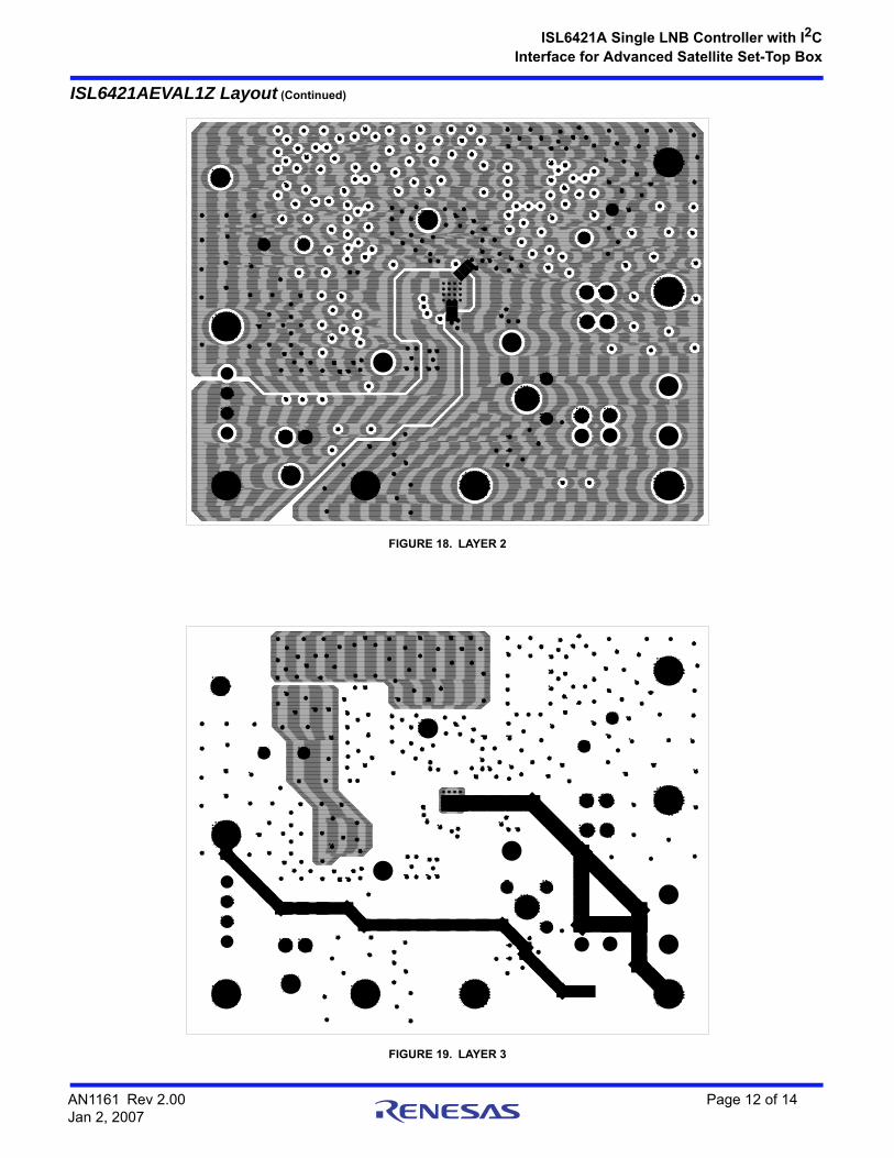
FIGURE 18. LAYER 2
FIGURE 19. LAYER 3
ISL6421AEVAL1Z Layout (Continued)
AN1161 Rev 2.00 Page 12 of 14Jan 2, 2007

ISL6421A Single LNB Controller with I2CInterface for Advanced Satellite Set-Top Box
FIGURE 20. LAYER 4
FIGURE 21. BOTTOM SILKSCREEN
ISL6421AEVAL1Z Layout (Continued)
AN1161 Rev 2.00 Page 13 of 14Jan 2, 2007

http://www.renesas.comRefer to "http://www.renesas.com/" for the latest and detailed information.
Renesas Electronics America Inc.1001 Murphy Ranch Road, Milpitas, CA 95035, U.S.A.Tel: +1-408-432-8888, Fax: +1-408-434-5351Renesas Electronics Canada Limited9251 Yonge Street, Suite 8309 Richmond Hill, Ontario Canada L4C 9T3Tel: +1-905-237-2004Renesas Electronics Europe LimitedDukes Meadow, Millboard Road, Bourne End, Buckinghamshire, SL8 5FH, U.KTel: +44-1628-651-700, Fax: +44-1628-651-804Renesas Electronics Europe GmbHArcadiastrasse 10, 40472 Düsseldorf, Germany Tel: +49-211-6503-0, Fax: +49-211-6503-1327Renesas Electronics (China) Co., Ltd.Room 1709 Quantum Plaza, No.27 ZhichunLu, Haidian District, Beijing, 100191 P. R. ChinaTel: +86-10-8235-1155, Fax: +86-10-8235-7679Renesas Electronics (Shanghai) Co., Ltd.Unit 301, Tower A, Central Towers, 555 Langao Road, Putuo District, Shanghai, 200333 P. R. China Tel: +86-21-2226-0888, Fax: +86-21-2226-0999Renesas Electronics Hong Kong LimitedUnit 1601-1611, 16/F., Tower 2, Grand Century Place, 193 Prince Edward Road West, Mongkok, Kowloon, Hong KongTel: +852-2265-6688, Fax: +852 2886-9022Renesas Electronics Taiwan Co., Ltd.13F, No. 363, Fu Shing North Road, Taipei 10543, TaiwanTel: +886-2-8175-9600, Fax: +886 2-8175-9670Renesas Electronics Singapore Pte. Ltd.80 Bendemeer Road, Unit #06-02 Hyflux Innovation Centre, Singapore 339949Tel: +65-6213-0200, Fax: +65-6213-0300Renesas Electronics Malaysia Sdn.Bhd.Unit 1207, Block B, Menara Amcorp, Amcorp Trade Centre, No. 18, Jln Persiaran Barat, 46050 Petaling Jaya, Selangor Darul Ehsan, MalaysiaTel: +60-3-7955-9390, Fax: +60-3-7955-9510Renesas Electronics India Pvt. Ltd.No.777C, 100 Feet Road, HAL 2nd Stage, Indiranagar, Bangalore 560 038, IndiaTel: +91-80-67208700, Fax: +91-80-67208777Renesas Electronics Korea Co., Ltd.17F, KAMCO Yangjae Tower, 262, Gangnam-daero, Gangnam-gu, Seoul, 06265 KoreaTel: +82-2-558-3737, Fax: +82-2-558-5338
SALES OFFICES
© 2018 Renesas Electronics Corporation. All rights reserved.Colophon 7.0
(Rev.4.0-1 November 2017)
Notice
1. Descriptions of circuits, software and other related information in this document are provided only to illustrate the operation of semiconductor products and application examples. You are fully responsible for
the incorporation or any other use of the circuits, software, and information in the design of your product or system. Renesas Electronics disclaims any and all liability for any losses and damages incurred by
you or third parties arising from the use of these circuits, software, or information.
2. Renesas Electronics hereby expressly disclaims any warranties against and liability for infringement or any other claims involving patents, copyrights, or other intellectual property rights of third parties, by or
arising from the use of Renesas Electronics products or technical information described in this document, including but not limited to, the product data, drawings, charts, programs, algorithms, and application
examples.
3. No license, express, implied or otherwise, is granted hereby under any patents, copyrights or other intellectual property rights of Renesas Electronics or others.
4. You shall not alter, modify, copy, or reverse engineer any Renesas Electronics product, whether in whole or in part. Renesas Electronics disclaims any and all liability for any losses or damages incurred by
you or third parties arising from such alteration, modification, copying or reverse engineering.
5. Renesas Electronics products are classified according to the following two quality grades: “Standard” and “High Quality”. The intended applications for each Renesas Electronics product depends on the
product’s quality grade, as indicated below.
"Standard": Computers; office equipment; communications equipment; test and measurement equipment; audio and visual equipment; home electronic appliances; machine tools; personal electronic
equipment; industrial robots; etc.
"High Quality": Transportation equipment (automobiles, trains, ships, etc.); traffic control (traffic lights); large-scale communication equipment; key financial terminal systems; safety control equipment; etc.
Unless expressly designated as a high reliability product or a product for harsh environments in a Renesas Electronics data sheet or other Renesas Electronics document, Renesas Electronics products are
not intended or authorized for use in products or systems that may pose a direct threat to human life or bodily injury (artificial life support devices or systems; surgical implantations; etc.), or may cause
serious property damage (space system; undersea repeaters; nuclear power control systems; aircraft control systems; key plant systems; military equipment; etc.). Renesas Electronics disclaims any and all
liability for any damages or losses incurred by you or any third parties arising from the use of any Renesas Electronics product that is inconsistent with any Renesas Electronics data sheet, user’s manual or
other Renesas Electronics document.
6. When using Renesas Electronics products, refer to the latest product information (data sheets, user’s manuals, application notes, “General Notes for Handling and Using Semiconductor Devices” in the
reliability handbook, etc.), and ensure that usage conditions are within the ranges specified by Renesas Electronics with respect to maximum ratings, operating power supply voltage range, heat dissipation
characteristics, installation, etc. Renesas Electronics disclaims any and all liability for any malfunctions, failure or accident arising out of the use of Renesas Electronics products outside of such specified
ranges.
7. Although Renesas Electronics endeavors to improve the quality and reliability of Renesas Electronics products, semiconductor products have specific characteristics, such as the occurrence of failure at a
certain rate and malfunctions under certain use conditions. Unless designated as a high reliability product or a product for harsh environments in a Renesas Electronics data sheet or other Renesas
Electronics document, Renesas Electronics products are not subject to radiation resistance design. You are responsible for implementing safety measures to guard against the possibility of bodily injury, injury
or damage caused by fire, and/or danger to the public in the event of a failure or malfunction of Renesas Electronics products, such as safety design for hardware and software, including but not limited to
redundancy, fire control and malfunction prevention, appropriate treatment for aging degradation or any other appropriate measures. Because the evaluation of microcomputer software alone is very difficult
and impractical, you are responsible for evaluating the safety of the final products or systems manufactured by you.
8. Please contact a Renesas Electronics sales office for details as to environmental matters such as the environmental compatibility of each Renesas Electronics product. You are responsible for carefully and
sufficiently investigating applicable laws and regulations that regulate the inclusion or use of controlled substances, including without limitation, the EU RoHS Directive, and using Renesas Electronics
products in compliance with all these applicable laws and regulations. Renesas Electronics disclaims any and all liability for damages or losses occurring as a result of your noncompliance with applicable
laws and regulations.
9. Renesas Electronics products and technologies shall not be used for or incorporated into any products or systems whose manufacture, use, or sale is prohibited under any applicable domestic or foreign laws
or regulations. You shall comply with any applicable export control laws and regulations promulgated and administered by the governments of any countries asserting jurisdiction over the parties or
transactions.
10. It is the responsibility of the buyer or distributor of Renesas Electronics products, or any other party who distributes, disposes of, or otherwise sells or transfers the product to a third party, to notify such third
party in advance of the contents and conditions set forth in this document.
11. This document shall not be reprinted, reproduced or duplicated in any form, in whole or in part, without prior written consent of Renesas Electronics.
12. Please contact a Renesas Electronics sales office if you have any questions regarding the information contained in this document or Renesas Electronics products.
(Note 1) “Renesas Electronics” as used in this document means Renesas Electronics Corporation and also includes its directly or indirectly controlled subsidiaries.
(Note 2) “Renesas Electronics product(s)” means any product developed or manufactured by or for Renesas Electronics.