AN11058 Design migration from TDA8024 to TDA8035 · AN11058 Design migration from TDA8024 to...
24
AN11058 Design migration from TDA8024 to TDA8035 Rev. 1.0 — 1 June 2011 Application note Document information Info Content Keywords TDA8035, TDA8024, migration, double implementation Abstract This application note describes how to migrate a design from TDA8024 to TDA8035: SW updates, HW differences, and an example based on a double layout implementation.
Transcript of AN11058 Design migration from TDA8024 to TDA8035 · AN11058 Design migration from TDA8024 to...

AN11058
Design migration from TDA8024 to TDA8035 Rev. 1.0 — 1 June 2011 Application note
Document information Info Content Keywords TDA8035, TDA8024, migration, double implementation
Abstract This application note describes how to migrate a design from TDA8024 to TDA8035: SW updates, HW differences, and an example based on a double layout implementation.
NXP Semiconductors AN11058 Design migration from TDA8024 to TDA8035
AN11058 All information provided in this document is subject to legal disclaimers. © NXP B.V. 2011. All rights reserved.
Application note Rev. 1.0 — 1 June 2011 2 of 24
Contact information For additional information, please visit: http://www.nxp.com For sales office addresses, please send an email to: [email protected]
Revision history Rev Date Description 1.0 20110601 First version
NXP Semiconductors AN11058 Design migration from TDA8024 to TDA8035
AN11058 All information provided in this document is subject to legal disclaimers. © NXP B.V. 2011. All rights reserved.
Application note Rev. 1.0 — 1 June 2011 3 of 24
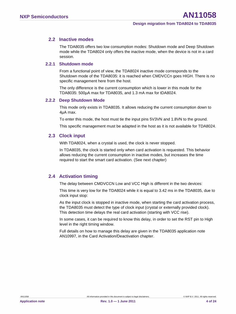
1. Introduction The TDA8024 is one of the most used Contact Smart Card readers in the Pay TV market.
It has been used for more than 10 years and has created a standard in contact reader front-end interfaces for Set Top Boxes.
The TDA8035 is a successor of this device that fully supports the same functionalities and brings some additional features.
For the Set Top Boxes that traditionally use the TDA8024, it is now recommended to switch from TDA8024 to TDA8035 in the new designs.
The goal of this document is to: • Present the differences between TDA8024 and TDA8035. • List all the modifications that should apply to design the TDA8035 instead of
TDA8024. • Propose an implementation where TDA8024 and TDA8035 can be mounted on the
same PCB.
2. Differences TDA8024 – TDA8035
2.1 Summary
Table 1. TDA8024 – TDA8035 differences summary Item TDA8024 TDA8035 Comments Package SO28 or TSSOP28 HVQFN32 -
Inactive mode No Shutdown mode 2 Shutdown modes: Automatic SD mode and Deep SD mode
New feature of TDA8035 for lower current consumption in inactive mode
Crystal clock input Crystal never stopped Crystal stopped when no card activation
New TDA8035 feature for lower current consumption
Activation timing No delay between CMDVCCN Low and VCC High
Typ. 3.4 ms delay between CMDVCCN Low and VCC High
Delay due to the crystal stop feature
DC/DC converter Doubler mode Tripler mode
Internal regulator (VREG)
No internal regulator Internal regulator for core power supply
VREG output on TDA8035 must be decoupled
Power supply strategy 2 power supply sources generally required
1 power supply source is generally enough
-
Presence pins 2 presence pins PRES (active high) and PRESN (active low)
1 presence pin PRESN (active low)
-
Chip select pin (CS) No chip select pin 1 Chip select pin Several TDA8035 can be cascaded.
Card class support Classes A and B (5V and 3V) Class A, B and C (5V, 3V, 1.8V) -
NXP Semiconductors AN11058 Design migration from TDA8024 to TDA8035
AN11058 All information provided in this document is subject to legal disclaimers. © NXP B.V. 2011. All rights reserved.
Application note Rev. 1.0 — 1 June 2011 4 of 24
2.2 Inactive modes The TDA8035 offers two low consumption modes: Shutdown mode and Deep Shutdown mode while the TDA8024 only offers the inactive mode, when the device is not in a card session.
2.2.1 Shutdown mode From a functional point of view, the TDA8024 inactive mode corresponds to the Shutdown mode of the TDA8035: it is reached when CMDVCCn goes HIGH. There is no specific management here from the host.
The only difference is the current consumption which is lower in this mode for the TDA8035: 500µA max for TDA8035, and 1.3 mA max for tDA8024.
2.2.2 Deep Shutdown Mode This mode only exists in TDA8035. It allows reducing the current consumption down to 4µA max.
To enter this mode, the host must tie the input pins 5V3VN and 1.8VN to the ground.
This specific management must be adapted in the host as it is not available for TDA8024.
2.3 Clock input With TDA8024, when a crystal is used, the clock is never stopped.
In TDA8035, the clock is started only when card activation is requested. This behavior allows reducing the current consumption in inactive modes, but increases the time required to start the smart card activation. (See next chapter)
2.4 Activation timing The delay between CMDVCCN Low and VCC High is different in the two devices:
This time is very low for the TDA8024 while it is equal to 3.42 ms in the TDA8035, due to clock input stop:
As the input clock is stopped in inactive mode, when starting the card activation process, the TDA8035 must detect the type of clock input (crystal or externally provided clock). This detection time delays the real card activation (starting with VCC rise).
In some cases, it can be required to know this delay, in order to set the RST pin to High level in the right timing window.
Full details on how to manage this delay are given in the TDA8035 application note AN10997, in the Card Activation/Deactivation chapter.

NXP Semiconductors AN11058 Design migration from TDA8024 to TDA8035
AN11058 All information provided in this document is subject to legal disclaimers. © NXP B.V. 2011. All rights reserved.
Application note Rev. 1.0 — 1 June 2011 5 of 24
2.5 DC/DC (SBM/SBP) Both chips embed a DC/DC converter based on capacitor, but with one difference:
The TDA8024 can only work as voltage level doubler, while TDA8035 can work as a tripler.
This difference has two impacts: • The TDA8035 has 2 more pins for the DC/DC converter: SBM and SBP (while SAM
and SAP correspond to S1 and S2 of the TDA8024). A capacitor must be connected between these SBM and SBP pins.
• The TDA8035 thanks to this extra capacitor can generate a 5V power supply for the smart card with a power supply input down to 2.7V, while TDA8024 requires 4V to generate the 5V in the standard conditions (up to 65 mA).
2.6 Internal Regulator VREG The TDA8035 embeds an internal regulator to supply the core of the IC with 1.8V. This regulator’s output is available on pin VREG to be decoupled with a 100nF capacitor.
This capacitor is to add in a new design upgraded from TDA8024 to TDA8035.
2.7 Power Supply strategy Thanks to the two additional features of the TDA8035 described above (DC/DC in tripler mode and internal regulator), it is possible to supply the TDA8035 with a single source, which corresponds to the CPU digital interface power supply level.
For example, if the host interface is applied with 3.3V, then this 3.3V can be used to supply the TDA8035’s host interface, the IC core, and the DC/DC converter
This was generally not the case with TDA8024, which requires a 4V for the DC/DC converter.
2.8 PORADJ PORADJ can be used in the same way in both chips when it is used, but the connection is different when PORADJ is not used:
For TDA8024, PORADJ must be connected to GND
For TDA8035, PORADJ must be connected to VDDI
NXP Semiconductors AN11058 Design migration from TDA8024 to TDA8035
AN11058 All information provided in this document is subject to legal disclaimers. © NXP B.V. 2011. All rights reserved.
Application note Rev. 1.0 — 1 June 2011 6 of 24
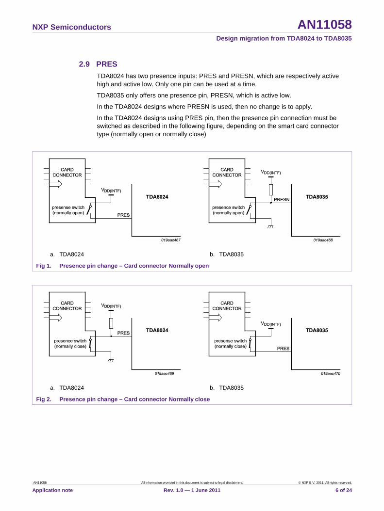
2.9 PRES TDA8024 has two presence inputs: PRES and PRESN, which are respectively active high and active low. Only one pin can be used at a time.
TDA8035 only offers one presence pin, PRESN, which is active low.
In the TDA8024 designs where PRESN is used, then no change is to apply.
In the TDA8024 designs using PRES pin, then the presence pin connection must be switched as described in the following figure, depending on the smart card connector type (normally open or normally close)
a. TDA8024 b. TDA8035
Fig 1. Presence pin change – Card connector Normally open
a. TDA8024 b. TDA8035
Fig 2. Presence pin change – Card connector Normally close
NXP Semiconductors AN11058 Design migration from TDA8024 to TDA8035
AN11058 All information provided in this document is subject to legal disclaimers. © NXP B.V. 2011. All rights reserved.
Application note Rev. 1.0 — 1 June 2011 7 of 24
2.10 CS TDA8035 has a Chip Select pin, allowing cascading as many devices in parallel as wanted.
In the case only one TDA8035 is needed, this pin must stay connected to VDDI. This is the case for a design where TDA8035 replaces TDA8024
2.11 1.8V TDA8035 supports 1.8V smart cards, while the TDA8024 does not support them.
This feature uses one pin: EN1.8VN. The connection of this pin in TDA8035 design depends on the new requirements for deep shutdown mode, and of course 1.8V cards management.
If the deep shutdown mode or the 1.8V card management is required, then this pin must be connected to a host GPIO.
If neither the deep shutdown mode nor the 1.8V card management is required, then this pin must be connected to VDDI.
3. New Design Summary In case of new design switching from TDA8024 to TDA8035, the following items must be checked and updated if required:
Table 2. TDA8024 to TDA8035 migration checklist Item HW/SW Description Comment Deep shutdown mode SW Add a state in the TDA device driver Only if the new feature Deep Shutdown
Mode is required
Activation timing SW Update the activation timings management (CMDVCCn / RSTIN)
Only if the RST assertion must respect a timing constraint
DC/DC new capacitor HW Add a 100 nF capacitor between SBM and SBP for the DC/DC converter
Mandatory
VREG capacitor HW Add a 100 nF capacitor on VREG for the internal regulator
Mandatory
Single power supply source
HW Use only one power supply for all TDA8035 blocks.
Optional
PORADJ HW Connect PORADJ to VDDI instead of GND
Only if PORADJ functionality is not used
PRES pin HW Change the presence detection management
Mandatory if PRES is used on TDA8024 No change if PRESN is used
CS HW Connect CS of the TDA8035 Mandatory
1.8V HW Connect EN1.8VN to VDDI or to a GPIO of the host
Mandatory to VDDI if no deep shutdown mode used and no 1.8V card management. GPIO else.

NXP Semiconductors AN11058 Design migration from TDA8024 to TDA8035
AN11058 All information provided in this document is subject to legal disclaimers. © NXP B.V. 2011. All rights reserved.
Application note Rev. 1.0 — 1 June 2011 8 of 24
4. Double Layout implementation For new design where the TDA8024 must be implemented in a first step (for timing, qualification… reasons), it is possible to design both TDA8024 and TDA8035 on the same PCB, allowing a reduced workload to switch once the TDA8035 has been fully qualified.
For this double implementation, some constraints must be respected, described here below.
The Cake8024_8035 evaluation board has been developed to demonstrate this use and show an example of this double implementation.
4.1 Demonstration board Cake8024_8035 This demonstration board implements a double layout, allowing it to accept any of the reader devices, in a reduced area.
The schematics and BOM for each product are shown and described in the following pages, as well as the single layout of the board.
This board layout has been designed using only 2 layers.
Fig 3. Cake8024_8035 in TDA8024 mode
NXP Semiconductors AN11058 Design migration from TDA8024 to TDA8035
AN11058 All information provided in this document is subject to legal disclaimers. © NXP B.V. 2011. All rights reserved.
Application note Rev. 1.0 — 1 June 2011 9 of 24
Fig 4. Cake8024_8035 in TDA8035 mode
Fig 5. Cake8024_8035 naked PCB

NXP Semiconductors AN11058 Design migration from TDA8024 to TDA8035
AN11058 All information provided in this document is subject to legal disclaimers. © NXP B.V. 2011. All rights reserved.
Application note Rev. 1.0 — 1 June 2011 10 of 24
4.1.1 Cake8024_8035 schematics (TDA8024 mode)
Fig 6. Cake8024_8035 schematics - TDA8024 mode

NXP Semiconductors AN11058 Design migration from TDA8024 to TDA8035
AN11058 All information provided in this document is subject to legal disclaimers. © NXP B.V. 2011. All rights reserved.
Application note Rev. 1.0 — 1 June 2011 11 of 24
4.1.2 Cake8024_8035 schematics (TDA8035 mode)
Fig 7. Cake8024_8035 schematics - TDA8035 mode
4.1.3 Cake8024_8035 BOM (TDA8024 mode)
Fig 8. Cake8024_8035 BOM - TDA8024 mode

NXP Semiconductors AN11058 Design migration from TDA8024 to TDA8035
AN11058 All information provided in this document is subject to legal disclaimers. © NXP B.V. 2011. All rights reserved.
Application note Rev. 1.0 — 1 June 2011 12 of 24
4.1.4 Cake8024_8035 BOM (TDA8035 mode)
Fig 9. Cake8024_8035 BOM - TDA8035 mode
NXP Semiconductors AN11058 Design migration from TDA8024 to TDA8035
AN11058 All information provided in this document is subject to legal disclaimers. © NXP B.V. 2011. All rights reserved.
Application note Rev. 1.0 — 1 June 2011 13 of 24
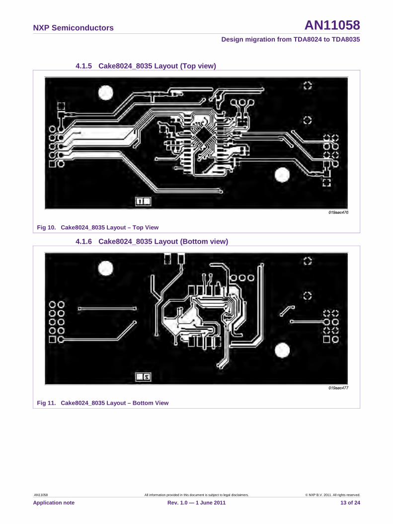
4.1.5 Cake8024_8035 Layout (Top view)
Fig 10. Cake8024_8035 Layout – Top View
4.1.6 Cake8024_8035 Layout (Bottom view)
Fig 11. Cake8024_8035 Layout – Bottom View
NXP Semiconductors AN11058 Design migration from TDA8024 to TDA8035
AN11058 All information provided in this document is subject to legal disclaimers. © NXP B.V. 2011. All rights reserved.
Application note Rev. 1.0 — 1 June 2011 14 of 24
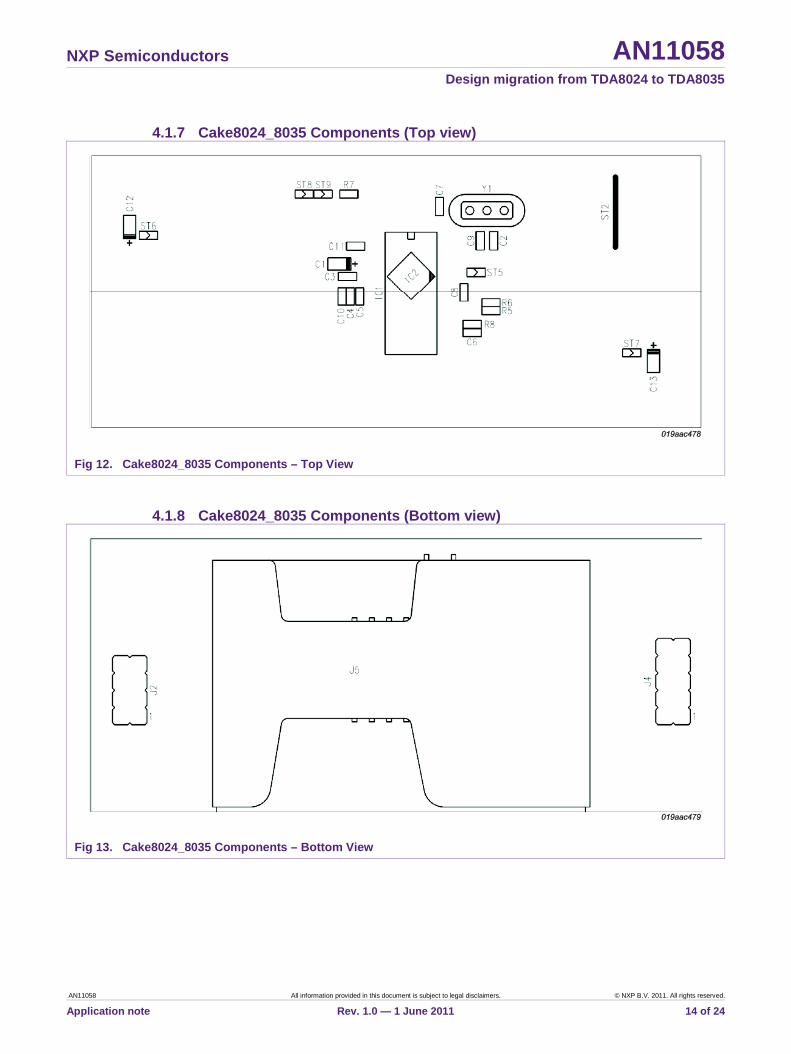
4.1.7 Cake8024_8035 Components (Top view)
Fig 12. Cake8024_8035 Components – Top View
4.1.8 Cake8024_8035 Components (Bottom view)
Fig 13. Cake8024_8035 Components – Bottom View
NXP Semiconductors AN11058 Design migration from TDA8024 to TDA8035
AN11058 All information provided in this document is subject to legal disclaimers. © NXP B.V. 2011. All rights reserved.
Application note Rev. 1.0 — 1 June 2011 15 of 24
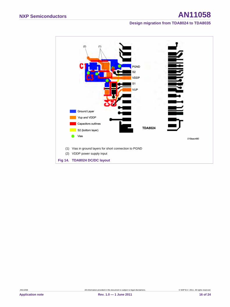
4.2 Double Implementation constraints 4.2.1 DC/DC converter
The DC/DC converter is one of the most critical parts when designing on of these devices. There are two main reasons that require taking a special care of this design part: • A bad DC/DC layout generates noise that can disturb other signals in the PCB • The DC/DC layout, if not correctly grounded, can disturb itself and stop functioning.
This is mainly the case with TDA8024 which has a quite sensitive DC/DC block.
The general rules to implement a DC/DC layout are: • Short connections • Very short and low resistive connection between the DC/DC external components
(capacitors) and its dedicated ground pin (GNDP or PGND)
In this double implementation layout, the first part to design is the DC/DC layout for TDA8024, which is the most critical part.
The Vup capacitor, and the VDDP decoupling, must have a maximum attention, in order to respect the above rules.
Then the TDA8035 must be placed in order to have its dedicated DC/DC pins as close as possible to the TDA8024’s DC/DC pins.
The figure next page is an extract of the board layout, where the routing of the TDA8024 DC/DC is highlighted. Other signals are removed for easier understanding.
The first step to design this layout is to place the capacitors for VDDP (C1 and C3), VUP (C4), and S1-S2 (C5).
Then the track from the pin to its dedicated capacitor must be routed as short as possible.
Finally, the connection between these capacitors and the ground pin PGND (DC/DC dedicated ground pin) must be as short as possible. Basically it has to be the shortest ground connection (shorter than connection to CGND or GND pin (pin #14 and pin #22).
NXP Semiconductors AN11058 Design migration from TDA8024 to TDA8035
AN11058 All information provided in this document is subject to legal disclaimers. © NXP B.V. 2011. All rights reserved.
Application note Rev. 1.0 — 1 June 2011 16 of 24
(1) Vias in ground layers for short connection to PGND (2) VDDP power supply input
Fig 14. TDA8024 DC/DC layout

NXP Semiconductors AN11058 Design migration from TDA8024 to TDA8035
AN11058 All information provided in this document is subject to legal disclaimers. © NXP B.V. 2011. All rights reserved.
Application note Rev. 1.0 — 1 June 2011 17 of 24
Once these signals have been routed, the TDA8035 can be placed, with short distance between TDA8035’s DC/DC pins and TDA8024’s DC/DC pins.
The remaining capacitors for the TDA8035 must then be placed as close as possible to the ICs. (C10 for SBM/SBP, and C141 for VREG)
On the next figure, the layout of the TDA8035 has been added to show the coexistence of both layouts.
(1) TDA8035’s VREG pin (2) TDA8035’s GNDP pin (3) TDA8035’s VDDP pin (4) TDA8035’s VUP pin
Fig 15. TDA8024 + TDA8035 DC/DC layout
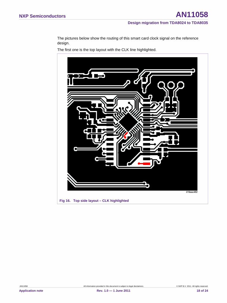
4.2.2 Smart card signals The second main constraint that must be respected is the layout of the smart card signals.
Depending on the application and the targeted market, these signals may be monitored for certification (e.g. NDS…). These signals must have a low noise level to pass most of the certifications.
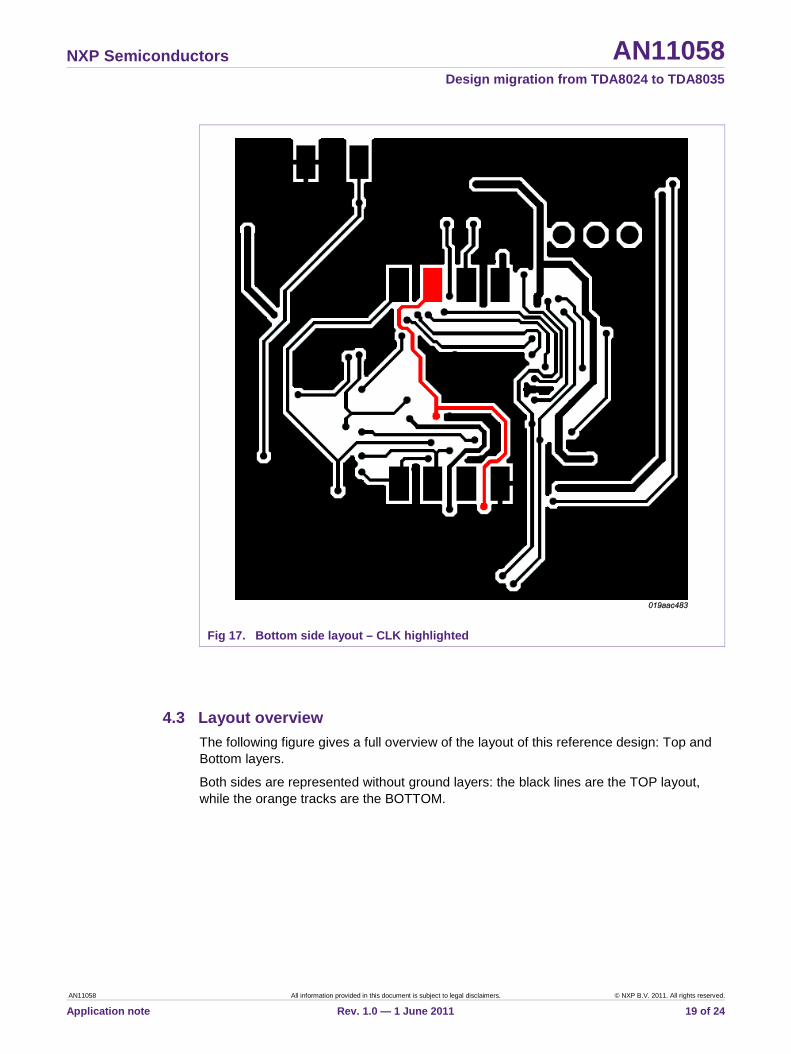
The main reason that causes noise on the smart card signals is the crosstalk between the signal and the clock line. Then the CLK line from the TDA to the smart card must be as short as possible and be kept far from other signals.
If possible, this line must be shielded with ground layers on each side.
NXP Semiconductors AN11058 Design migration from TDA8024 to TDA8035
AN11058 All information provided in this document is subject to legal disclaimers. © NXP B.V. 2011. All rights reserved.
Application note Rev. 1.0 — 1 June 2011 18 of 24
The pictures below show the routing of this smart card clock signal on the reference design.
The first one is the top layout with the CLK line highlighted.
Fig 16. Top side layout – CLK highlighted
NXP Semiconductors AN11058 Design migration from TDA8024 to TDA8035
AN11058 All information provided in this document is subject to legal disclaimers. © NXP B.V. 2011. All rights reserved.
Application note Rev. 1.0 — 1 June 2011 19 of 24
Fig 17. Bottom side layout – CLK highlighted
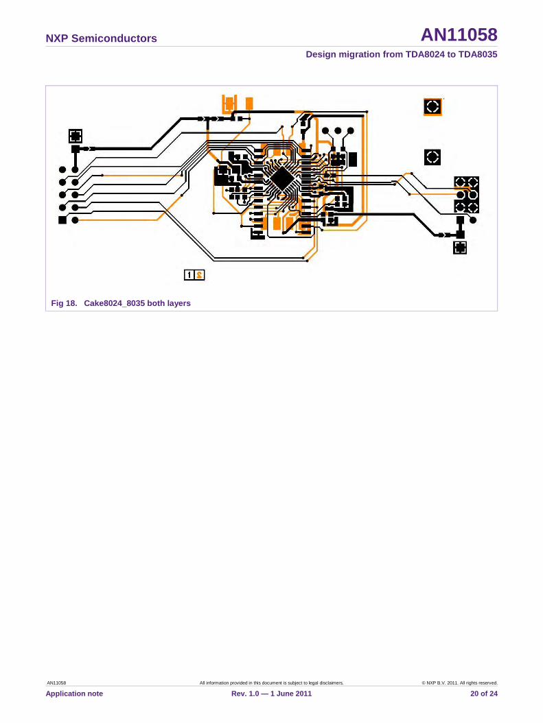
4.3 Layout overview The following figure gives a full overview of the layout of this reference design: Top and Bottom layers.
Both sides are represented without ground layers: the black lines are the TOP layout, while the orange tracks are the BOTTOM.
NXP Semiconductors AN11058 Design migration from TDA8024 to TDA8035
AN11058 All information provided in this document is subject to legal disclaimers. © NXP B.V. 2011. All rights reserved.
Application note Rev. 1.0 — 1 June 2011 20 of 24
Fig 18. Cake8024_8035 both layers

Error! U
nknown docum
ent property nam
e.
Error! Unknow
n document property nam
e. Error! U
nknown docum
ent property
NXP Semiconductors AN11058 Design migration from TDA8024 to TDA8035
AN11058 All information provided in this document is subject to legal disclaimers. © NXP B.V. 2011. All rights reserved.
Application note Rev. 1.0 — 1 June 2011 21 of 24
5. Legal information
5.1 Definitions Draft — The document is a draft version only. The content is still under internal review and subject to formal approval, which may result in modifications or additions. NXP Semiconductors does not give any representations or warranties as to the accuracy or completeness of information included herein and shall have no liability for the consequences of use of such information.
5.2 Disclaimers Limited warranty and liability — Information in this document is believed to be accurate and reliable. However, NXP Semiconductors does not give any representations or warranties, expressed or implied, as to the accuracy or completeness of such information and shall have no liability for the consequences of use of such information.
In no event shall NXP Semiconductors be liable for any indirect, incidental, punitive, special or consequential damages (including - without limitation - lost profits, lost savings, business interruption, costs related to the removal or replacement of any products or rework charges) whether or not such damages are based on tort (including negligence), warranty, breach of contract or any other legal theory.
Notwithstanding any damages that customer might incur for any reason whatsoever, NXP Semiconductors’ aggregate and cumulative liability towards customer for the products described herein shall be limited in accordance with the Terms and conditions of commercial sale of NXP Semiconductors.
Right to make changes — NXP Semiconductors reserves the right to make changes to information published in this document, including without limitation specifications and product descriptions, at any time and without notice. This document supersedes and replaces all information supplied prior to the publication hereof.
Suitability for use — NXP Semiconductors products are not designed, authorized or warranted to be suitable for use in life support, life-critical or safety-critical systems or equipment, nor in applications where failure or malfunction of an NXP Semiconductors product can reasonably be expected to result in personal injury, death or severe property or environmental damage. NXP Semiconductors accepts no liability for inclusion and/or use of
NXP Semiconductors products in such equipment or applications and therefore such inclusion and/or use is at the customer’s own risk.
Applications — Applications that are described herein for any of these products are for illustrative purposes only. NXP Semiconductors makes no representation or warranty that such applications will be suitable for the specified use without further testing or modification.
Customers are responsible for the design and operation of their applications and products using NXP Semiconductors products, and NXP Semiconductors accepts no liability for any assistance with applications or customer product design. It is customer’s sole responsibility to determine whether the NXP Semiconductors product is suitable and fit for the customer’s applications and products planned, as well as for the planned application and use of customer’s third party customer(s). Customers should provide appropriate design and operating safeguards to minimize the risks associated with their applications and products.
NXP Semiconductors does not accept any liability related to any default, damage, costs or problem which is based on any weakness or default in the customer’s applications or products, or the application or use by customer’s third party customer(s). Customer is responsible for doing all necessary testing for the customer’s applications and products using NXP Semiconductors products in order to avoid a default of the applications and the products or of the application or use by customer’s third party customer(s). NXP does not accept any liability in this respect.
Export control — This document as well as the item(s) described herein may be subject to export control regulations. Export might require a prior authorization from national authorities.
5.3 Trademarks Notice: All referenced brands, product names, service names and trademarks are property of their respective owners.
NXP Semiconductors AN11058 Design migration from TDA8024 to TDA8035
AN11058 All information provided in this document is subject to legal disclaimers. © NXP B.V. 2011. All rights reserved.
Application note Rev. 1.0 — 1 June 2011 22 of 24
6. List of figures
Fig 1. Presence pin change – Card connector Normally open ................................................... 6
Fig 2. Presence pin change – Card connector Normally close .................................................. 6
Fig 3. Cake8024_8035 in TDA8024 mode .................. 8Fig 4. Cake8024_8035 in TDA8035 mode .................. 9Fig 5. Cake8024_8035 naked PCB ............................. 9Fig 6. Cake8024_8035 schematics -
TDA8024 mode ............................................... 10Fig 7. Cake8024_8035 schematics -
TDA8035 mode ............................................... 11Fig 8. Cake8024_8035 BOM - TDA8024 mode ........ 11Fig 9. Cake8024_8035 BOM - TDA8035 mode ........ 12Fig 10. Cake8024_8035 Layout – Top View ............... 13Fig 11. Cake8024_8035 Layout – Bottom View .......... 13Fig 12. Cake8024_8035 Components – Top View ...... 14Fig 13. Cake8024_8035 Components – Bottom View 14Fig 14. TDA8024 DC/DC layout .................................. 16Fig 15. TDA8024 + TDA8035 DC/DC layout ............... 17Fig 16. Top side layout – CLK highlighted .................. 18Fig 17. Bottom side layout – CLK highlighted ............. 19Fig 18. Cake8024_8035 both layers ........................... 20
NXP Semiconductors AN11058 Design migration from TDA8024 to TDA8035
AN11058 All information provided in this document is subject to legal disclaimers. © NXP B.V. 2011. All rights reserved.
Application note Rev. 1.0 — 1 June 2011 23 of 24
7. List of tables
Table 1. TDA8024 – TDA8035 differences summary ...... 3Table 2. TDA8024 to TDA8035 migration checklist ........ 7
NXP Semiconductors AN11058 Design migration from TDA8024 to TDA8035
Please be aware that important notices concerning this document and the product(s) described herein, have been included in the section 'Legal information'.
© NXP B.V. 2011. All rights reserved.
For more information, please visit: http://www.nxp.com For sales office addresses, please send an please send an email to: [email protected]
Date of release: 1 June 2011 Document identifier: AN11058
8. Contents
1. Introduction ......................................................... 3 2. Differences TDA8024 – TDA8035 ....................... 3 2.1 Summary ............................................................ 3 2.2 Inactive modes ................................................... 4 2.2.1 Shutdown mode ................................................. 4 2.2.2 Deep Shutdown Mode ........................................ 4 2.3 Clock input ......................................................... 4 2.4 Activation timing ................................................. 4 2.5 DC/DC (SBM/SBP) ............................................ 5 2.6 Internal Regulator VREG ................................... 5 2.7 Power Supply strategy ....................................... 5 2.8 PORADJ............................................................. 5 2.9 PRES ................................................................. 6 2.10 CS ...................................................................... 7 2.11 1.8V .................................................................... 7 3. New Design Summary ......................................... 7 4. Double Layout implementation .......................... 8 4.1 Demonstration board Cake8024_8035 .............. 8 4.1.1 Cake8024_8035 schematics (TDA8024 mode) 10 4.1.2 Cake8024_8035 schematics (TDA8035 mode) 11 4.1.3 Cake8024_8035 BOM (TDA8024 mode) ......... 11 4.1.4 Cake8024_8035 BOM (TDA8035 mode) ......... 12 4.1.5 Cake8024_8035 Layout (Top view) ................. 13 4.1.6 Cake8024_8035 Layout (Bottom view) ............ 13 4.1.7 Cake8024_8035 Components (Top view) ........ 14 4.1.8 Cake8024_8035 Components (Bottom view) ... 14 4.2 Double Implementation constraints .................. 15 4.2.1 DC/DC converter .............................................. 15 4.2.2 Smart card signals ........................................... 17 4.3 Layout overview ............................................... 19 5. Legal information .............................................. 21 5.1 Definitions ........................................................ 21 5.2 Disclaimers....................................................... 21 5.3 Trademarks ...................................................... 21 6. List of figures ..................................................... 22 7. List of tables ...................................................... 23 8. Contents ............................................................. 24