An Overview of Signal Source Technology and...
32
® An Overview of Signal Source Technology and Applications ®
Transcript of An Overview of Signal Source Technology and...

®
An Overv iew of S ignal
Source Technology and
Appl icat ions
®


An Overv iew of S ignal
Source Technology and
Appl icat ions
Who Should Read This PrimerThis publication is aimed at engineers and technicians involved in the develop-ment of just about any kind of product with electronic content. If your jobresponsibilities include characterization, debug, verification, or testing of elec-tronic circuits that carry AC signals (waveforms), then you are very likely toneed a waveform source that can adapt to the unique needs of your design.
Often, the first breakthrough in a verification or troubleshooting task is findinga way to replicate the symptoms of a problem in your design. Usually thisinvolves a signal source of some kind. Understanding the many types of signalsources, their features and functions, and their applications can help youchoose a signal source that will deliver the waveforms you need. As always,selecting the right tool will make your job easier and will help you produce fast,reliable results.
i

ii

Contents
Who Should Read This Primer · · · · · · · · · · · · · · · · · · · · · · · · · · · · · · · · · · · · · · · · · · · · · · · · · · · · · · · · · · · · · i
What is a Signal Source? · · · · · · · · · · · · · · · · · · · · · · · · · · · · · · · · · · · · · · · · · · · · · · · · · · 1Types of Digital Signal Sources · · · · · · · · · · · · · · · · · · · · · · · · · · · · · · · · · · · · · · · · · · · · · · · · · · · · · · · · · · · · 1
Signal Source Hardware Architecture: The Arbitrary Waveform Generator · · · · · · · 3Doing the Math: Clock Frequency and Memory Depth Calculations · · · · · · · · · · · · · · · · · · · · · · · · · · · · · · 4Modifying the Waveform: Filtering and Sequencing · · · · · · · · · · · · · · · · · · · · · · · · · · · · · · · · · · · · · · · · · · · 5Creating AWG Waveforms: Tools and Methods · · · · · · · · · · · · · · · · · · · · · · · · · · · · · · · · · · · · · · · · · · · · · · · · 6Summary · · · · · · · · · · · · · · · · · · · · · · · · · · · · · · · · · · · · · · · · · · · · · · · · · · · · · · · · · · · · · · · · · · · · · · · · · · · · · · 7
Signal Source Hardware Architecture: The Arbitrary Function Generator · · · · · · · · 9Understanding Direct Digital Synthesis · · · · · · · · · · · · · · · · · · · · · · · · · · · · · · · · · · · · · · · · · · · · · · · · · · · · · · 9Summary · · · · · · · · · · · · · · · · · · · · · · · · · · · · · · · · · · · · · · · · · · · · · · · · · · · · · · · · · · · · · · · · · · · · · · · · · · · · · 10
Signal Source Hardware Architecture: The Data Generator· · · · · · · · · · · · · · · · · · · · 11Digital Patterns Differ from Analog Waveforms · · · · · · · · · · · · · · · · · · · · · · · · · · · · · · · · · · · · · · · · · · · · · · 12Sequencer Expands Pattern Length Indefinitely · · · · · · · · · · · · · · · · · · · · · · · · · · · · · · · · · · · · · · · · · · · · · · 12A Sharp Tool for Digital Faults · · · · · · · · · · · · · · · · · · · · · · · · · · · · · · · · · · · · · · · · · · · · · · · · · · · · · · · · · · · · 13Analog Parameters in a Digital World · · · · · · · · · · · · · · · · · · · · · · · · · · · · · · · · · · · · · · · · · · · · · · · · · · · · · · 14Making the Connection · · · · · · · · · · · · · · · · · · · · · · · · · · · · · · · · · · · · · · · · · · · · · · · · · · · · · · · · · · · · · · · · · · 15Summary · · · · · · · · · · · · · · · · · · · · · · · · · · · · · · · · · · · · · · · · · · · · · · · · · · · · · · · · · · · · · · · · · · · · · · · · · · · · · 15
Signal Source Applications· · · · · · · · · · · · · · · · · · · · · · · · · · · · · · · · · · · · · · · · · · · · · · · 17AWG Application: Simulating a Disk Drive Read-Channel Signal · · · · · · · · · · · · · · · · · · · · · · · · · · · · · · · 17AWG Application: Simulating Real-World Aberrations in 100Base-T Physical Layer Signals · · · · · · · · 19Data Generator Application: Rambus® Design and Troubleshooting · · · · · · · · · · · · · · · · · · · · · · · · · · · · · 21
Design margin testing · · · · · · · · · · · · · · · · · · · · · · · · · · · · · · · · · · · · · · · · · · · · · · · · · · · · · · · · · · · · · · · · · 21Clock Substitution · · · · · · · · · · · · · · · · · · · · · · · · · · · · · · · · · · · · · · · · · · · · · · · · · · · · · · · · · · · · · · · · · · · 21Testing Complementary Signal Paths · · · · · · · · · · · · · · · · · · · · · · · · · · · · · · · · · · · · · · · · · · · · · · · · · · · · 21Dispelling the Effects of Ground Bounce and Transients · · · · · · · · · · · · · · · · · · · · · · · · · · · · · · · · · · · · 21
Some Signal Source Characteristics and Capabilities to Watch For · · · · · · · · · · · · · 22Characteristics · · · · · · · · · · · · · · · · · · · · · · · · · · · · · · · · · · · · · · · · · · · · · · · · · · · · · · · · · · · · · · · · · · · · · · · · · 22
Sample Rate · · · · · · · · · · · · · · · · · · · · · · · · · · · · · · · · · · · · · · · · · · · · · · · · · · · · · · · · · · · · · · · · · · · · · · · · · 22Vertical Resolution · · · · · · · · · · · · · · · · · · · · · · · · · · · · · · · · · · · · · · · · · · · · · · · · · · · · · · · · · · · · · · · · · · · 22Memory Depth · · · · · · · · · · · · · · · · · · · · · · · · · · · · · · · · · · · · · · · · · · · · · · · · · · · · · · · · · · · · · · · · · · · · · · 22Number of Channels · · · · · · · · · · · · · · · · · · · · · · · · · · · · · · · · · · · · · · · · · · · · · · · · · · · · · · · · · · · · · · · · · · 22
Capabilities · · · · · · · · · · · · · · · · · · · · · · · · · · · · · · · · · · · · · · · · · · · · · · · · · · · · · · · · · · · · · · · · · · · · · · · · · · · · 22Modifying AWG Waveforms in Real Time: Integrated Editors · · · · · · · · · · · · · · · · · · · · · · · · · · · · · · · · 22Creating Application-Specific Waveforms: Dedicated Functions · · · · · · · · · · · · · · · · · · · · · · · · · · · · · 22Expanding the Waveform Length: Sequencing · · · · · · · · · · · · · · · · · · · · · · · · · · · · · · · · · · · · · · · · · · · · · 23Synchronizing Analog and Digital: Markers · · · · · · · · · · · · · · · · · · · · · · · · · · · · · · · · · · · · · · · · · · · · · · · 23Using Waveforms from Other Resources: Importing Data · · · · · · · · · · · · · · · · · · · · · · · · · · · · · · · · · · · · 23
Signal Source Selection Guide · · · · · · · · · · · · · · · · · · · · · · · · · · · · · · · · · · · · · · · · · · · · 24
The Integrated Tool Set for Superior Measurement and Analysis · · · · · · · · back cover
iii
An Overview of Signal Source Technology and Applications

iv

A signal source is nothing less than the cornerstoneof almost any instrumentation setup used in hard-ware design, debug, or evaluation projects. It is a keyengineering tool. It is an essential troubleshootingaid for the technician. It is a surrogate for an automo-tive ignition pulse, a heart pacemaker, or a guidedmissile’s gyro output. Second only to the ubiquitousDMM, signal sources are perhaps the most universalclass of electronic test instruments.
Unless you’re working with a purely DC circuit (andwhen was the last time you designed a flashlight?),your circuit is likely to require some kind of ACstimulus signal as you evaluate components, func-tional blocks, and subsystems. The waveform fromthe signal source emulates a signal coming in fromthe outside world, such as a sensor output. Similarly,it can be used as a stand-in for waveforms that willappear in as-yet-unavailable parts of the circuitdesign.
Interestingly, the signal source’s job is not simply toprovide an “ideal” waveform. Often the instrumentmust add known, repeatable amounts and types ofdistortion (or errors) to the signal it delivers. Thischaracteristic is one of the signal source’s strongestvirtues, since it is often impossible to createpredictable distortion exactly when and where it’sneeded using only the circuit itself. The response ofthe unit-under-test (UUT) in the presence of thesedistorted signals reveals its ability to handle stressesthat fall outside the normal performance envelope.
A stimulus signal may take the form of a low-distortion sine wave, a stream of logic pulses, a high-frequency radio carrier wave, a mobile telephonetransmission, and many other formats. Traditionally,the task of producing these diverse waveforms hasbeen filled by separate, dedicated signal sources,from ultra-pure audio sine-wave generators to multi-GHz RF signal generators. While there are manycommercial solutions, the user must often custom-design or modify a signal source for the project athand. It can be very difficult to design an instrumen-tation-quality signal generator, and of course, thetime spent designing ancillary test equipment is acostly distraction from the project itself.
Fortunately, digital sampling technology and signalprocessing techniques have brought us a solutionthat answers almost any kind of signal generationneed with just one type of instrument – the arbitrarygenerator.
Types of Digital Signal SourcesBroadly divided into arbitrary waveform generators(AWG), arbitrary function generators (AFG), and dataor pattern generators (DG), digital signal sourcesspan the whole range of signal-producing needs.Each of these types has its unique strengths:• AWG: Whether you want a data stream shaped by
a precise Lorentzian pulse for disk-drive charac-terization, or a complex modulated RF signal totest a GSM- or CDMA-based telephone handset,the AWG can produce any waveform you canimagine. You can use a variety of methods – frommathematical formulae to “drawing” the wave-form – to create the needed output.
• AFG: Typically this instrument offers fewer wave-form variations, but with excellent stability andfast response to frequency changes. If the UUTrequires the classic “sine and square” waveforms(to name a few) and the ability to switch almostinstantly between two frequencies, the AFG is theright tool. An additional virtue is the AFG’s lowcost, which makes it very attractive for applica-tions that do not require an AWG’s versatility.
• DG: This third type of signal source meets thespecial stimulus needs of digital devices thatrequire long, continuous streams of binary data,with specific information content and timingcharacteristics. The rationale for this specializedtype of signal source will become evident in thearchitectural discussions that follow.
Earlier, we described signal sources as a class ofuniversal test instruments. With the advent of AWGsand AFGs in particular, the term “universal” takeson an even broader meaning, since many differentsignal generation tasks conceivably can be handlednot by one class of instruments, but by just oneinstrument.
1
What is a Signal Source?

2
3
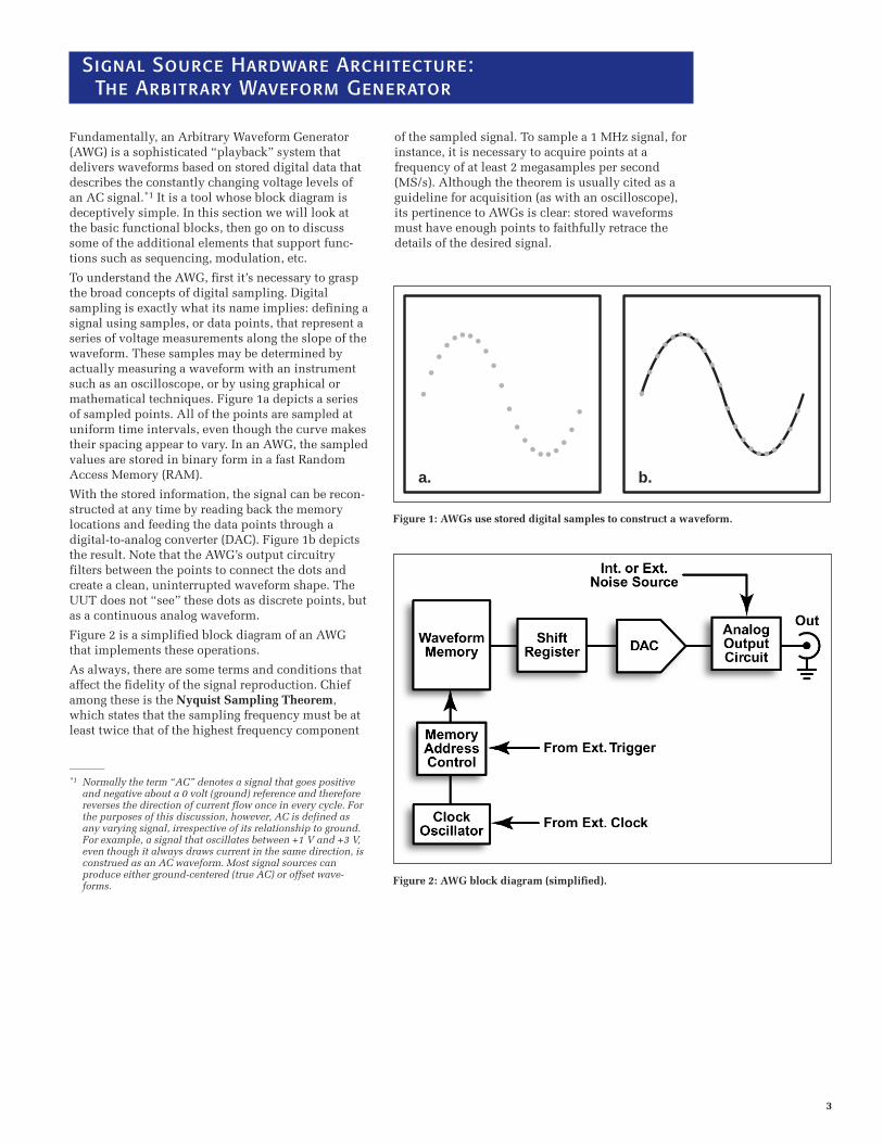
Fundamentally, an Arbitrary Waveform Generator(AWG) is a sophisticated “playback” system thatdelivers waveforms based on stored digital data thatdescribes the constantly changing voltage levels ofan AC signal.*1 It is a tool whose block diagram isdeceptively simple. In this section we will look atthe basic functional blocks, then go on to discusssome of the additional elements that support func-tions such as sequencing, modulation, etc.
To understand the AWG, first it’s necessary to graspthe broad concepts of digital sampling. Digitalsampling is exactly what its name implies: defining asignal using samples, or data points, that represent aseries of voltage measurements along the slope of thewaveform. These samples may be determined byactually measuring a waveform with an instrumentsuch as an oscilloscope, or by using graphical ormathematical techniques. Figure 1a depicts a seriesof sampled points. All of the points are sampled atuniform time intervals, even though the curve makestheir spacing appear to vary. In an AWG, the sampledvalues are stored in binary form in a fast RandomAccess Memory (RAM).
With the stored information, the signal can be recon-structed at any time by reading back the memorylocations and feeding the data points through adigital-to-analog converter (DAC). Figure 1b depictsthe result. Note that the AWG’s output circuitryfilters between the points to connect the dots andcreate a clean, uninterrupted waveform shape. TheUUT does not “see” these dots as discrete points, butas a continuous analog waveform.
Figure 2 is a simplified block diagram of an AWGthat implements these operations.
As always, there are some terms and conditions thataffect the fidelity of the signal reproduction. Chiefamong these is the Nyquist Sampling Theorem,which states that the sampling frequency must be atleast twice that of the highest frequency component
of the sampled signal. To sample a 1 MHz signal, forinstance, it is necessary to acquire points at afrequency of at least 2 megasamples per second(MS/s). Although the theorem is usually cited as aguideline for acquisition (as with an oscilloscope),its pertinence to AWGs is clear: stored waveformsmust have enough points to faithfully retrace thedetails of the desired signal.
Figure 1: AWGs use stored digital samples to construct a waveform.
a. b.
Figure 2: AWG block diagram (simplified).
Signal Source Hardware Architecture:The Arbitrary Waveform Generator
__________
*1 Normally the term “AC” denotes a signal that goes positiveand negative about a 0 volt (ground) reference and thereforereverses the direction of current flow once in every cycle. Forthe purposes of this discussion, however, AC is defined asany varying signal, irrespective of its relationship to ground.For example, a signal that oscillates between +1 V and +3 V,even though it always draws current in the same direction, isconstrued as an AC waveform. Most signal sources canproduce either ground-centered (true AC) or offset wave-forms.

4
An AWG can take these points and read them out ofmemory at any frequency within its specified limits.If a set of stored points conforms to the NyquistTheorem and describes a sine wave, then the AWG’soutput will be a sine wave. However, there is a finitemaximum frequency, or sample rate, at which theinstrument can operate. This is usually specified interms of megasamples or gigasamples per second.Today’s fastest AWGs can achieve 2.6 GS/s.
Other AWG hardware characteristics, particularlyvertical resolution and memory depth, are just asimportant as sample rate.
Vertical resolution (amplitude) expresses thevoltage-measuring precision of the sample pointsdescribed above. Resolution pertains to the binaryword width, in bits, of the instrument’s DAC, withmore bits equating to higher resolution. While “moreis better,” higher-frequency AWGs usually havelower resolution – 8 or 10 bits – than general-purpose AWGs offering 12 or 14 bits.
An AWG with 10-bit resolution provides 1024sample levels spread across the full voltage range ofthe instrument. If, for example, this 10-bit AWG hasa total voltage range of 2 Vp-p, each sample repre-sents a step of approximately 2 mV – the smallestincrement the instrument could deliver, assuming itis not constrained by other factors in its architecture.
Memory depth in an AWG plays a key role in theinstrument’s flexibility. More (deeper) memoryprovides either of two benefits: 1) More cycles of the desired waveform can be
stored. This is useful because it reduces thenumber of “endpoints.” An endpoint is the lastmemory location occupied by the waveform, afterwhich the AWG must wrap around and return tothe beginning in order to continue to produce theoutput signal. There are unavoidable errors thatoccur at this transition, so it is desirable to mini-mize the number of endpoints.
2) More waveform detail can be stored. Complexwaveforms have high-frequency information intheir pulse edges and transients. It is difficult tointerpolate these fast transitions as we did withthe simple, predictable sine wave. To faithfully
reproduce a complex signal, the available wave-form memory capacity must be used to store moretransitions and fluctuations rather than morecycles of the signal.
Today’s state-of-the-art AWGs offer up to 8-Msamplememory depth. When combined with the highsample rate that some top models deliver, theseinstruments can store and reproduce complex RFwaveforms, even including pseudo-random bitstreams for use in physical-layer testing of networkequipment. Similarly, these fast AWGs with deepmemory can generate very brief digital pulses andtransients.
Doing the Math: Clock Frequency andMemory Depth CalculationsCalculating the frequency of the waveform that anAWG will produce is a matter of solving a fewsimple equations. Consider the example of an instru-ment with one waveform cycle stored in memory:
Given a 100 MS/s clock frequency and a memorydepth of 4000 samples – an actual sample RAMwould have 4096 samples, but we will round thatfigure to 4000 for the sake of simplicity – then:
Foutput = Clock Frequency ÷ Memory Depth
Foutput = 100,000,000 ÷ 4000
Foutput = 25,000 Hz (or 25 kHz)
Figure 3 illustrates this concept.
Figure 3: At a clock frequency of 100 MHz, the single 4000-point waveform is delivered as a 25 kHz output signal.
4000 Points

5
At the stated clock frequency, the samples are about10 ns apart. This is the time resolution (horizontal)of the waveform. Be sure not to confuse this with theamplitude resolution (vertical) described earlier.
Carrying this process a step further, assume that thesample RAM contains not one, but four cycles of thewaveform:
Foutput = (Clock Frequency ÷ Memory Depth) x (cycles inmemory)
Foutput = (100,000,000 ÷ 4000) x (4)
Foutput = (25,000 Hz) x (4)
Foutput = 100,000 Hz
The new frequency is 100 kHz, and we have reducedthe number of endpoint transitions. Figure 4 depictsthis concept.
In this instance, the time resolution of each waveformcycle is lower than that of the single-waveformexample – in fact, it is exactly four times lower. Eachsample now represents 40 ns in time. The increase infrequency (and the reduction in endpoint aberrations)comes at the cost of some horizontal resolution.
Modifying the Waveform: Filteringand SequencingOnce the basic waveform is defined, other operationscan be applied to modify or extend it.
Filtering allows you to remove selected bands offrequency content from the signal. For example,when testing an analog-to-digital converter (ADC), itis necessary to ensure that the analog input signal(which comes from the AWG) is free of frequencieshigher than the converter’s clock frequency. Thisprevents unwanted aliasing distortion in the UUToutput, which would otherwise compromise the testresults.
One reliable way to eliminate these frequencies is toapply a steep low-pass filter to the waveform. Thisallows frequencies below a specified point to passthrough, and drastically attenuates those above thecutoff.
Filters also can be used to “roll off” pure waveformssuch as square and triangle waves. Sometimes it’ssimpler to modify an existing waveform in this waythan to create a new one.
In the past, it was necessary to use a signal generatorand an external filter to achieve results such asthese. Fortunately, the better present-day laboratoryAWGs feature accurate built-in filters.
Waveform sequencing is another valuable enhance-ment to the basic AWG architecture. In effect, itallows you to store a huge number of “virtual” wave-form cycles in the instrument’s memory. The wave-form sequencer borrows instructions from thecomputer world: loops, jumps, and so forth. Theseinstructions, which reside in a sequence memoryseparate from the waveform memory, cause specifiedsegments of the waveform memory to repeat. Figure 4: Using four stored waveforms and a 100 MHz
clock, a 100 kHz signal is produced.
4000 Points

6
To cite a very simple example, imagine that the4000-point memory described earlier is loaded witha clean pulse that takes up half the memory (2000points), and a distorted pulse that uses the remaininghalf. If we were limited to basic repetition of thememory content, then the AWG would always repeatthe two pulses, in order, until commanded to stop.But waveform sequencing changes all that.
Suppose you wanted the distorted pulse to appeartwice in succession after every 511 cycles. You couldwrite a sequence that repeats the clean pulse 511times, then jumps to the distorted pulse, repeats ittwice, and goes back to the beginning to loopthrough the steps again… and again. Figure 5explains this premise. Loop repetitions can go intothe hundreds of millions. Given what we havealready discussed about the tradeoff between thenumber of cycles stored and the resulting horizontalresolution, it’s clear that sequencing provides much-improved flexibility without compromising the reso-lution of individual waveforms.
Note here that any sequenced waveform segmentmust continue from the same amplitude point as thesegment preceding it. In other words, if a sine wavesegment’s last sample value was 1.2 volts, thestarting value of the next segment in the sequencemust be 1.2 volts as well. Otherwise, an undesirableglitch can occur when the DAC attempts to abruptlychange to the new value.
Although this example is very basic, it represents thekind of capability that is needed to detect irregularpattern-dependent errors and co-symbol interferencein communications circuits. With waveformsequencing, it’s possible to run long-term stress tests– extending to days or even weeks – with the AWGas the stimulus source.
Creating AWG Waveforms: Tools andMethodsWe have discussed the AWG’s ability to producelong, complex waveforms. But this would be almostuseless if the engineer had to key in point-by-pointvalues for every location in the waveform memory.Fortunately, there are many labor-saving approachesto waveform creation.
Most lab-quality AWGs are furnished with certainstandard waveforms, either stored in the instru-ment’s local nonvolatile memory, or provided ondisk media. These waveforms make an excellentstarting point for modification via the AWG’s editingtools.
One of the most efficient ways to derive a new wave-form is to “learn” it from a digital sampling oscillo-scope (DSO). If, for example, stimulus signals areneeded for testing a newly-developed product inmanufacturing, the DSO can be used to capture thewaveforms from a known-good engineering proto-type. The DSO’s acquisition memory contents canthen be copied into the AWG’s sample memory via aGPIB or Ethernet connection between the two instru-ments. Assuming the AWG has sufficient bandwidthand resolution, it can duplicate the waveformexactly. Perhaps just as important, the AWG’s wave-form can be modified with known impairments, ifnecessary.
A second waveform creation method is the AWG’sbuilt-in math tool. All “standard” waveforms (sine,square, triangle, etc.) can be derived from relativelysimple mathematical formulae. Some AWGs havemath editors that apply convolution, integration, andother operations. As an adjunct to this on-boardmath capability, many AWGs accept data from PC-based waveform simulation tools.
Figure 5: AWG waveform memory capacity can be “expanded” with loops and repetitions.
Repeat 511 times
Repeat 2 times
Repeat
Start
Finish
1,000times

7
The third, and perhaps the most intriguing, wave-form editing method is the built-in graphical editor.Some AWGs offer a means of actually drawing (onthe instrument’s own display screen) the waveformfeatures you need. Of course there are finite limita-tions – you still can’t make an edge transition in0 ps! – but the instrument will reproduce all of thewaveform details within its performance range.Figure 6 is a typical graphical waveform editingdisplay.
Some AWGs can actually deliver an analog wave-form output and a correlated digital signal at thesame time. These instruments have “marker”outputs that can provide either a trigger pulse or aprogrammed binary expression when a specificsample value is clocked out of the memory.
SummaryThe arbitrary waveform generator (AWG) offers adegree of versatility that few instruments can match.With its ability to produce any waveform you canimagine, the AWG embraces applications rangingfrom automotive ABS simulation to wirelessnetwork stress testing. The AWG is a tool that nodesign or development lab should be without.
Figure 6: AWG graphical waveform editor.

8
The arbitrary function generator (AFG) shares manyfeatures with the AWG, although the AFG is, bydesign, a more specialized instrument with anarrower range of applications. The AFG offersunique strengths: it produces stable waveforms instandard shapes – particularly the all-important sineand square waves – that are both accurate and agile.Agility is the ability to change quickly and cleanlyfrom one frequency to another.
Most AFGs offer some subset of the followingfamiliar wave shapes:• Sine• Square• Triangle• Sweep• Pulse• Ramp• Modulation• Noise• Haversine
While AWGs can certainly provide these same wave-forms, today’s AFGs are designed to provideimproved phase, frequency, and amplitude control ofthe output signal. Moreover, many AFGs offer a wayto modulate the signal from internal or externalsources, which is essential for some types of stan-dards compliance testing.
In the past, AFGs created their output signals usinganalog oscillators and signal conditioning. Morerecent AFGs rely on a completely different architec-
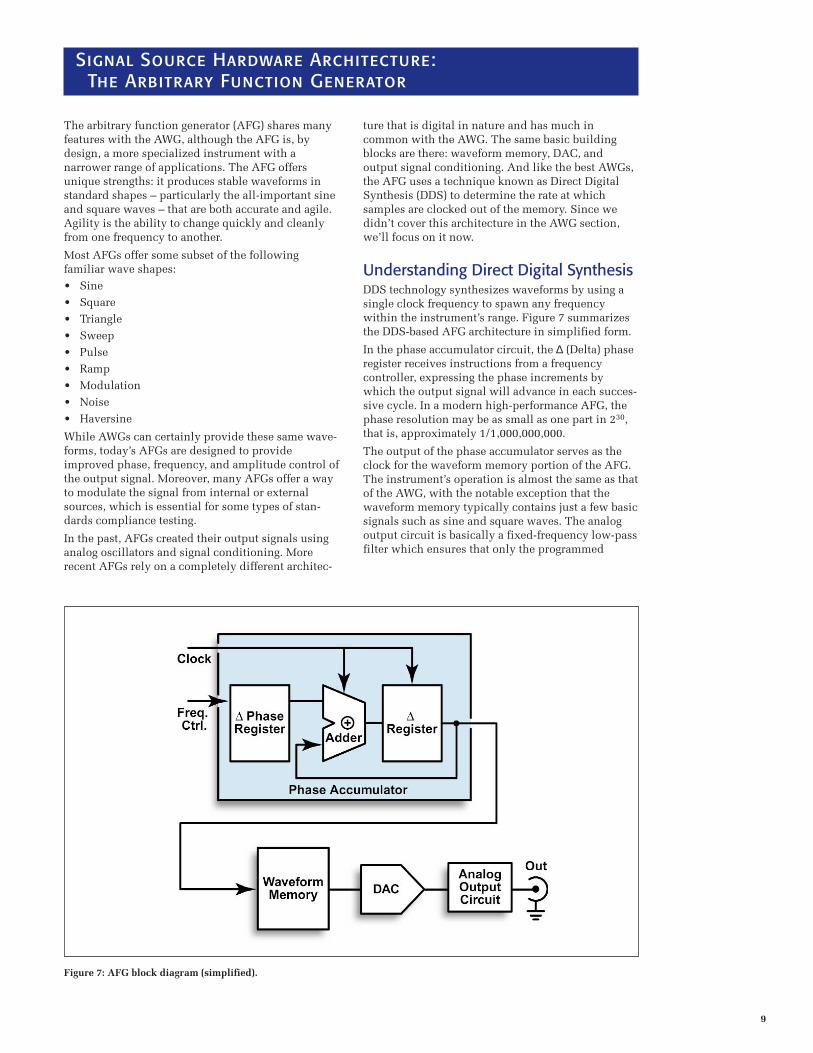
ture that is digital in nature and has much incommon with the AWG. The same basic buildingblocks are there: waveform memory, DAC, andoutput signal conditioning. And like the best AWGs,the AFG uses a technique known as Direct DigitalSynthesis (DDS) to determine the rate at whichsamples are clocked out of the memory. Since wedidn’t cover this architecture in the AWG section,we’ll focus on it now.
Understanding Direct Digital SynthesisDDS technology synthesizes waveforms by using asingle clock frequency to spawn any frequencywithin the instrument’s range. Figure 7 summarizesthe DDS-based AFG architecture in simplified form.
In the phase accumulator circuit, the ∆ (Delta) phaseregister receives instructions from a frequencycontroller, expressing the phase increments bywhich the output signal will advance in each succes-sive cycle. In a modern high-performance AFG, thephase resolution may be as small as one part in 230,that is, approximately 1/1,000,000,000.
The output of the phase accumulator serves as theclock for the waveform memory portion of the AFG.The instrument’s operation is almost the same as thatof the AWG, with the notable exception that thewaveform memory typically contains just a few basicsignals such as sine and square waves. The analogoutput circuit is basically a fixed-frequency low-passfilter which ensures that only the programmed
9
Signal Source Hardware Architecture:The Arbitrary Function Generator
Figure 7: AFG block diagram (simplified).

10
frequency of interest (and no clock artifacts) leavesthe AFG output.
To understand how the phase accumulator creates afrequency, imagine that the controller sends a valueof “1” to the 30-bit ∆ phase register. The phase accu-mulator’s ∆ output register will advance by 360 ÷ 230
in each cycle, since 360 degrees represents a fullcycle of the instrument’s output waveform.Therefore, a ∆ phase register value of “1” producesthe lowest-frequency waveform in the AFG’s range,requiring the full 230 increments to create one cycle.The circuit will remain at this frequency until a newvalue is loaded into the ∆ phase register.
Values greater than one will advance through the 360degrees more quickly, producing a higher outputfrequency (some AFGs use a different approach: theyincrease the output frequency by skipping somesamples, thereby reading the memory contentsfaster). Note that the only thing that changes is thephase value supplied by the frequency controller.The main clock frequency does not need to change atall. In addition, it allows a waveform to commencefrom any point in the waveform cycle.
For example, assume it is necessary to produce asine wave that begins at the peak of the positive-going part of the cycle. Basic math tells us that thispeak occurs at 90 degrees. Therefore:
2 30 increments = 360°; and
90° = 360° ÷ 4; then,
90° = 230 ÷ 4
When the phase accumulator receives a value equiv-alent to (230 ÷ 4), it will prompt the waveform
memory to start from a location containing the posi-tive peak voltage of the sine wave.
As explained earlier, the typical AFG has just a fewtypes of waveforms stored in its memory. In general,sine and square waves are the most widely used formany test applications. Some AFGs are “hybrid”units that deliver accurate, agile DDS-based sine andsquare waves, while other wave shapes are createdusing more conventional AWG techniques. This is acost-effective solution that puts the highest perfor-mance behind the most critical functions.
DDS architecture provides exceptional frequencyagility, making it easy to program both frequency andphase changes on the fly. Where is this important?Certainly it’s useful for testing any type of FM(frequency-modulated) UUT device – radio andsatellite system components, for example. And if thespecific AFG’s frequency range is sufficient, it’s anideal signal source for test on FSK (frequency shiftkeying) and frequency-hopping telephony technolo-gies such as GSM.
SummaryThe arbitrary function generator (AFG) serves a widerange of stimulus needs; in fact, it is the prevailingsignal-source architecture in the industry today.Although it cannot equal the AWG’s ability to createvirtually any imaginable waveform, the AFGproduces the most common test signals used in labs,repair facilities, and design departments around theworld. Moreover, it delivers excellent frequencyagility. And perhaps most important to many users,the AFG is available at a fraction of the price of topAWG models.

11
A third type of signal source, the data generator(DG), is a more specialized tool for those withspecific digital test requirements. Where the AWGand AFG are primarily designed to produce wave-forms with “analog” shapes and characteristics, theDG’s mission is to generate volumes of binary infor-mation. Also known as a pattern generator, the DGproduces the streams of 1s and 0s needed for testingcomputer busses, microprocessor IC devices, andother digital systems.
Because it is dedicated to digital testing applications,there might be a tendency to infer that the DG is a“limited” tool. After all, an AWG can generatepattern data but the DG cannot generate analogwaveforms! The DG was never meant to be auniversal tool; instead, its features give it uniquestrengths that neither AWGs nor AFGs can match.
Among these features are: • Sequencing: An absolute necessity in the world of
data and pattern generation. No internal memorycan be deep enough to store the many millions ofpattern words (also known as “vectors”) requiredfor a thorough digital-device test. Consequently,DGs are equipped with sophisticated sequencers,far more so than those of other types of signalsources.
• Multiple outputs: Where the AWG or AFG mayhave two or four outputs, the DG may havehundreds of output channels. This is to supportthe numerous data and/or address inputs of thetypical digital device.
• Pattern data sources: The modern DG mustaccept data from logic analyzers, DSOs, simula-tors, and even spreadsheets. Why? Because acomplex digital pattern would be impossiblytedious and error-prone if entered by hand.
Moreover, digital data is usually available fromvarious simulation and verifications steps in thedesign process.
• Display: The DG display must emphasize thedetails of many channels of pattern data simulta-neously rather than the details of signal ampli-tude vs. time (as with the AWG display). It shouldoffer markers, scrolling, and other time-savingfeatures to help the user focus on the data ofinterest. Figure 8 is an example of a multi-channel DG display.
Signal Source Hardware Architecture: The Data Generator
Figure 8: Multi-channel DG bus timing display.

12
Digital Patterns Differ fromAnalog WaveformsSome aspects of the DG architecture will lookfamiliar after reading the earlier sections on AWGsand AFGs. Figure 9 depicts the DG block diagram.Once again there is an address generator, a waveform(or pattern) memory, a shift register, etc. But noticeone significant omission: the DAC is absent!
The DAC is not necessary because the DG doesn’tneed to trace out the constantly shifting levels of ananalog waveform. Although the DG has an analogoutput circuit, this circuit is used to set voltage andedge parameters that apply to the whole pattern. Forexample, most DGs provide a way to program thelogic “1” and “0” voltage values for the pattern.
Sequencer Expands PatternLength IndefinitelyThe DG’s sequencer bears some similarity to that ofthe AWG described earlier. The DG must providetremendously long and complex patterns, and mustrespond to external events – usually a UUT outputcondition that prompts a branch execution in the DGsequencer.
The DG’s pattern memory capacity, typically about256 Kbits maximum, may seem modest in compar-ison to the largest AWG waveform memory. But likethe AWG sequencer, the DG sequencer can loop onshort pattern segments to produce a data stream ofmuch greater length. It can wait for an external eventor trigger, then execute a series of repeat counts or
Figure 9: DG block diagram (simplified).
13
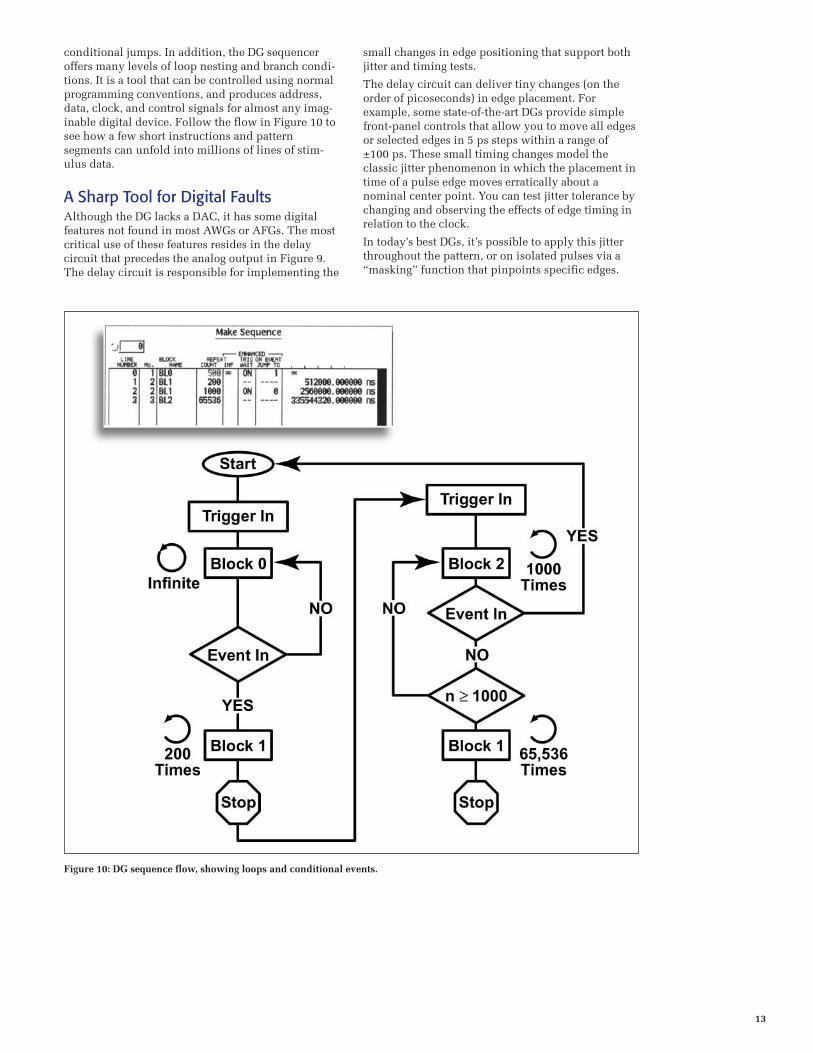
conditional jumps. In addition, the DG sequenceroffers many levels of loop nesting and branch condi-tions. It is a tool that can be controlled using normalprogramming conventions, and produces address,data, clock, and control signals for almost any imag-inable digital device. Follow the flow in Figure 10 tosee how a few short instructions and patternsegments can unfold into millions of lines of stim-ulus data.
A Sharp Tool for Digital FaultsAlthough the DG lacks a DAC, it has some digitalfeatures not found in most AWGs or AFGs. The mostcritical use of these features resides in the delaycircuit that precedes the analog output in Figure 9.The delay circuit is responsible for implementing the
small changes in edge positioning that support bothjitter and timing tests.
The delay circuit can deliver tiny changes (on theorder of picoseconds) in edge placement. Forexample, some state-of-the-art DGs provide simplefront-panel controls that allow you to move all edgesor selected edges in 5 ps steps within a range of±100 ps. These small timing changes model theclassic jitter phenomenon in which the placement intime of a pulse edge moves erratically about anominal center point. You can test jitter tolerance bychanging and observing the effects of edge timing inrelation to the clock.
In today’s best DGs, it’s possible to apply this jitterthroughout the pattern, or on isolated pulses via a“masking” function that pinpoints specific edges.
Figure 10: DG sequence flow, showing loops and conditional events.

14
Figure 11 shows a digital phosphor oscilloscope(DPO) capture of a DG output signal with the addi-tion of the jitter effect. The inset illustration providesa simplified and enlarged view of the same events.
Other features give the modern DG even more flexi-bility for critical jitter testing. Some instrumentshave an external analog modulation input thatcontrols both the amount of edge displacement (inpicoseconds) and the rate at which it occurs. With somany jitter variables at your disposal, it’s possible tosubject the UUT to a wide range of real-worldstresses.
The delay circuit plays a second, equally importantrole in testing for timing problems such as setup-and-hold violations. Most clocked devices requirethe data signal to be present for a few nanosecondsbefore the clock pulse appears (setup time), and toremain valid for a few nanoseconds (hold time) afterthe clock edge. The delay circuit makes it easy toimplement this set of conditions. Just as it can movea signal edge a few picoseconds at a time, it canmove that edge in hundreds of picoseconds, or innanoseconds. This is exactly what is needed to eval-uate setup and hold time. The test involves movingthe input data signal’s leading and trailing edges,respectively, a fraction of a nanosecond at a timewhile holding the clock edge steady. The resultingUUT output signal is acquired by a DSO or logicanalyzer. When the UUT begins to put out valid dataconsistent with the input condition, the location ofthe leading data edge is the setup time. Thisapproach can also be used to detect metastableconditions in which the UUT output is unpre-dictable.
Analog Parameters in a Digital WorldAlthough the DG’s repertoire does not includecommon signal conditioning operations such asfiltering and modulation, it nevertheless offers sometools to manipulate the output signal. These featuresare needed because digital design problems are notlimited to purely digital issues such as jitter andtiming violations. Some design faults are the resultof analog phenomena such as erratic voltage levels orslow edge rise times. The DG must be able to simu-late both.
Voltage variations in the stimulus signal are a keystress-testing tool. By exercising a digital UUT withvarying voltage level, especially levels immediatelybelow the device’s logic threshold, it is possible topredict the device’s performance and reliability as awhole. A UUT with intermittent (and difficult totrace) failures will almost certainly turn into a“hard” failure when the voltage is reduced.
Figure 12 depicts the effect of programming a DG toproduce several discrete logic levels. Here the resultsof several instructions are shown cumulatively, butin reality, the instrument applies a single voltagelevel throughout the pattern.
Edge transition times, or rise times, are anotherfrequent cause of problems in digital designs. Forexample, a pulse with a slow edge transition may nottrigger the next device in line in time to clock indata. Slow edges are notorious for causing raceconditions, another cause of intermittent failures. Ahost of cumulative design factors, notably distrib-uted reactances, can degrade the rise time of a pulseas it travels from source to destination. Therefore,engineers try to ensure that their circuits can handlea range of rise times. Like the voltage variationsdescribed earlier, slowing down the pulse edge rateis part of every stress and margin testing plan. Sincethe DG is a common tool in digital design environ-ments, it’s often called upon to simulate these transi-tion-time problems.
Figure 11: The DG uses small timing shifts to simulate jitter.
Figure 12: Programmed voltage variations on a DG output signal.

15
Looking again at the DG block diagram in Figure 9,notice the input labeled “Transient Control” thatfeeds the analog output circuit. It is here that theuser can program a broad range of edge rates for theinstrument’s output signal.
Figure 13 illustrates the effect of the programmableedge-rate feature.
Making the ConnectionAs we have discussed, DGs are often used in teststhat require critical pulse-edge characteristics,including voltage accuracy, rise-time performance,and edge placement. Unfortunately, simplyproviding a high-quality signal at the instrument’sfront-panel connector is not enough. Often the signalmust travel to a test fixture a meter or more awayfrom the instrument, through cables and connectorsthat can seriously degrade the signal’s timing andedge details. Some modern DGs solve this problemwith an external signal interface that buffers thesignal and brings the performance of the instrumentall the way out to the UUT.
Figure 14 shows a typical DG equipped with a signalinterface. The interface minimizes rise-time degrada-tions due to cable capacitance and provides amplelocal current to drive a UUT input without “loadingdown.” Interestingly, the external interface is theconnection point for signals from the UUT, notably“Inhibit” instructions that cause the DG output toswitch to a high-impedance state.
SummaryData Generator Applications Span ManyTechnologies. In the design department, the DG is anindispensable stimulus source for almost every classof digital device. In broader terms, the DG is usefulfor functional testing, debug of new designs, andfailure analysis of existing ones. It’s also an expe-dient tool to support timing and amplitude margincharacterization.
The DG can be used early in the product develop-ment cycle to substitute for system components thatare not yet available . For example, it might beprogrammed to send interrupts and data to a newlydeveloped bus circuit when the processor that wouldnormally provide the signals doesn’t yet exist.Similarly, the DG might provide addresses to amemory bus, or even the digital equivalent of a sinewave to a DAC under test.
With its extraordinarily long patterns and its abilityto implant occasional errors in the data stream, theDG can support long-term reliability tests to ensurecompliance with military or aerospace standards. Inaddition, its ability to respond to external eventsfrom the UUT as part of the pattern sequenceprovides even more flexibility in demanding charac-terization applications.
The DG is equally at home testing semiconductordevices such as ASICs and FPGAs, or rotating media– hard-disk drive write circuits and DVDs. Likewise,it’s useful for testing CCD image sensors and LCDdisplay drivers/controllers. The DG is an effectivesolution just about anywhere a complex digital bitstream is needed to stimulate a UUT.
Figure 13: Programmed rise-time variations on a DG output signal.
Figure 14: DGs and external signal interface “pod.”

16

17
AWG Application: Simulating a DiskDrive Read-Channel SignalWith their ever-increasing speed and bit density,hard-disk drives (HDD) pose one of the most formi-dable test challenges existent today. The AWG playsan enabling role in the design and evaluation of newgenerations of HDDs. It provides signals that modelthe response of a read channel, permitting engineersto move ahead with the design of all the ancillarycircuitry that delivers the disk data to the outsideworld.
The first step is to create an emulation of the transi-tion response that occurs when a read head acquiresdata from the magnetic medium. This signal takes onthe classic shape of a Lorentzian pulse.
To create the Lorentzian pulse, we can use an AWGwith an Equation Editor. The rationale for thespecific Lorentzian pulse formula is beyond thescope of this discussion*2, but suffice it to say thatthe following formula is required:
Where: t = timeT is a parameter representing the bitintervalPW50 is the pulse width at which theamplitude is at 50% of the peak voltage
Figure 15 shows this same formula as it appears onthe screen display, along with an inset image thatpresents the resulting Lorentzian pulse wave shape.
While entering the above formula will certainlyproduce the desired waveform, there may be a moreexpedient way to get the job done. Some AWGs aresupplied with a library of waveforms, either storedwithin a ROM in the instrument or on a floppy disk.Usually, it’s much simpler to modify one of thesefactory-supplied waveforms than to design yourown.
The next step is to create the actual binary datacontent using the AWG’s Pattern Editor tools. Thepattern has the fundamental period of the bit intervalT (from the formula above) and should reflect anycoding algorithms, such as RLL, that need to beapplied. In this example, we will use a 62-bit NRZ(Non-Return to Zero) pattern. Figure 16 shows thePattern Editor screen
After the pattern is entered via the editor, it’s neces-sary to scale the signal to match the target bitinterval. For the sake of simplicity, assume the datarate is 650 Mbps, so that each pattern bit represents1.5 ns. Using an AWG with a 2.6 GS/s clock rate,
each signal point represents six data points in theAWG memory. It’s necessary at this point to expandthe pattern to a 248-point record.
The image inset in Figure 16 shows the resultingdata stream.
__________*2 For more information, see Signals and Measurements for
Disk Drive Design at www.tektronix.com/Measurement/-App_Notes/.
Signal Source Applications
Figure 15: The AWG equation editor simplifies creation of the Lorentzian pulse.
Figure 16: The Pattern Editor’s tools create the needed binary information.

18
The final step in this process is to convolve the twosignals – the Lorentzian pulse and the data stream –to produce a detailed model of a genuine read-channel signal. This could be a complex mathemat-ical process, but once again, the AWG’s built-in toolscome to the rescue. State-of-the-art AWGs incorpo-rate a convolution tool that includes options such asdifferential math. This is exactly what we need toproduce the final waveform shape for the HDD readchannel.
The differential math is needed because the binarywaveform is a typical stream of 1 and 0 states, whilethe read channel’s information content is impartedby transitions, not states. The differentiation ensuresthat the final data reflects this reality. The result isshown in Figure 17.
There is an alternative approach to that describedabove. The AWG’s equation editor provides the toolsto enter the waveform in mathematical terms. Theeditor supports polynomial formulas made up ofmany operators, functions, and variables. Althoughit sounds complex, this approach can actuallysimplify the design of complex waveforms forcertain applications.
In addition to the steps outlined here, others may berequired to “fine tune” the waveform for its ultimateuse in a read channel. But the foregoing explanationhas shown you how an AWG can generate andmanipulate detailed read-channel waveforms.
Figure 18 shows the advanced disk-drive applicationeditor provided by the AWG610 and AWG500 series.The disk-drive application editor uses a fill-in-the-blanks approach to quickly and easily create read-channel signals for simulation and test of read-channel amplifiers and other devices.
Figure 17: The hard disk Read channel signal.
Figure 18: Advanced disk-drive application editor offered by the AWG610.

AWG Application: Simulating Real-World Aberrations in 100Base-TPhysical Layer Signals To simulate physical layer test signals for 100Base-Ttransceivers, you must consider a wealth of analogparameters: undershoot and overshoot, rise and falltime, ringing, amplitude variations, and specifictiming variations such as jitter. AWGs provide anefficient method for generating signal impairmentslike these and many more. Using an AWG to repli-cate 100Base-T Ethernet signal impairments is thebest way to stress components to the limits (margins)of their performance under real-world conditions.
The starting point for such a margin test is the100Base-T signal shown in Figure 19, which wascreated by a modern AWG with a built-in NetworkSignal Application Editor. The basis of this signal isa PN9 pseudo-random data stream. The screenshown here is from an oscilloscope measurement,not the AWG itself.
The AWG display screen in Figure 20 highlightssome of the built-in features of the application editorused to create a 100Base-T signal. Notice that youmay choose any of several protocol standards, fromITU-T to SDH/SONET, as well as the bit rate, linecode (MLT-3 in this example), and other parameters.
19
Figure 20: The network signal application editor screen.
Figure 19: An application-specific network signal editor on an AWG was used to createthis 100Base-T signal.

20
In Figure 21, the 100Base-T signal shows the effectsof amplitude variations applied with a real-timeediting tool built into the AWG.
By adding momentary amplitude attenuations likethis, it is possible to characterize the UUT’s responseto varying degrees of signal loss due to harsh real-world conditions, and adapt the design accordingly.Note also the lower trace, which is the AWG’s markeroutput. It was used here to trigger the oscilloscopewhich captured this display.
Figure 21: Real-time editing tools can be used to apply brief signal variations.

21
Data Generator Application: Rambus®
Design and TroubleshootingDemand for video and audio web applications onpersonal computers has spawned a requirement forhigh-bandwidth memory that can keep pace withother system elements, especially processors andbuses. In answer to this need, Rambus®, Inc. hasdeveloped a new memory architecture known as the(RDRAM™) which can outperform current SDRAMtechnology by a factor of ten.
Rambus’ approach to providing increased memorysystem performance is based on a high-speed, chip-to-chip interface that transfers data over a relativelynarrow bus known as the Rambus Channel. RDRAMdevices support a transfer rate of 800 Mbps on eachof the data pins.
At these tremendous data rates, tolerances can buildup, ground bounce phenomena can emerge, andsignals can deteriorate. It may be difficult to pin theblame on any one part of the circuit.
We have talked about measuring setup/hold timesand jitter, for example. But what is the recoursewhen there is too much jitter? Jitter is a symptom –what is causing the symptom? Other potential prob-lems range from improper clock and data waveformsymmetry to excessive noise on the transmissionlines.
The modern DG can augment measurement toolssuch as oscilloscopes and logic analyzers to resolveRambus design problems. They can help find theroot cause of problems that seem to have no clearorigin. The process is one of signal substitution andfault isolation.
To be effective in the Rambus environment, the DGmust deliver exceptional performance at highfrequencies. Data rates in the range of 1.1 Gb/s areessential. In addition, the DG must provide an ultra-low-jitter signal (preferably in the range of 3 ps) withedge risetimes of 150 ps or less. To carry out certainstress tests, the DG must deliver a wide range ofsignal amplitudes – approximately 0.25 Vp-p to2.5 Vp-p. Programmable channel-to-channel delayand complementary outputs are also useful for thedifferential signal lines common in Rambus architec-ture. Following are some applications that makegood use of a DG:
Design margin testingEven a design that “works” has its limits. What arethose limits? It’s mandatory to confirm that thedesign offers sufficient margin to manage thevagaries of the manufacturing process. Tolerancebuildup in clock signal path terminations and deviceAC parameters is another common problem in high-speed circuits.
A DG can stress system elements with signals thatare too early, too late, too “small” (in amplitude),and so on.
Clock SubstitutionMemory-access failures can have many causes. Onesuch cause is setup and hold timing violations dueto excessive clock jitter. By substituting an externallow-jitter source for the clock that feeds theRDRAMs, it’s possible to “divide and conquer” thecircuit problem.
Figure 22 is a jitter characterization of a DG output,measuring only 12.170 ps jitter. The measurementwas taken with a high-bandwidth oscilloscope. Sinceactual Rambus Channel jitter is in the 70 ps range (orhigher), it’s obvious that this DG is capable ofhandling Rambus clock substitution chores.
Testing Complementary Signal PathsA DG with programmable complementary outputscan provide paired signals to evaluate the effects ofamplitude variations, skew between RambusChannel Clock To Master (CTM) and Clock FromMaster (CFM) signals, and symmetry referenced toVref.
Dispelling the Effects of GroundBounce and TransientsSimultaneous bus access across a multi-channelRambus system draws far more current than usual,causing ground bounce and possibly voltage tran-sients that are echoed in the CTM signal line.
An external DG can usually provide much greatercurrent source and sink capacity than the on-boardclock generator. This extra output capacity offersgreater resistance to waveform deformation, permit-ting the designer to evaluate the effects of a moreperfect clock in the circuit.
Figure 22: A low-jitter signal from an external DG can be used for Rambus clocksubstitution during troubleshooting.

22
CharacteristicsA host of factors must be weighed when choosing asignal source. Of course, the “banner” specificationsare important. However, you need to also look at theinstrument’s adaptability to your particular applica-tion. It’s very easy to be swayed by sample rates andresolution specifications when the tool you reallyneed is the one that can accept your EDA simulatordata.
Most published specifications dwell on the keymeasures of signal source performance – the“banner” specifications – leaving the determinationof adaptability up to your discernment.
The key specifications, in order of importance, are asfollows:
Sample RateThe maximum clock or sample rate at which theinstrument can operate. The sample rate controls thefrequency and fidelity of the main output signal. TheNyquist Theorem states that the clock rate must be atleast twice the frequency of the desired signal’shighest component frequency to ensure accuratereproduction. Four, eight, or even 100 times over-sampling may be necessary in some applications.
Vertical ResolutionThe vertical resolution of the DAC defines the ampli-tude accuracy and distortion of the reproducedwaveform. A DAC with inadequate resolutioncontributes to quantization errors, causing imperfectwaveform generation.
Memory DepthMemory depth limits the length of a non-repeatingwaveform. It contributes to signal fidelity becauseusing a low-frequency signal (relative to the sampleclock rate) permits more data points to be stored percycle. Without sufficient memory depth, you cannottake advantage of the high relative sample rate.Modern AWGs offer 2, 4, even 8 Msamples ofmemory.
Number of ChannelsMany applications require more than one outputchannel. AWGs with up to four independent chan-nels are available. This feature is indispensable forsimulating sensors in automotive (anti-lock brakes)
or bio-electrical applications, and more. Similarly,dual-channel instruments can generate complexdigital modulation signals such as I&Q modulatedwaveforms. Some AWGs have one or two analogoutputs and up to 14 high-speed digital outputs formixed-signal testing.
CapabilitiesAfter you’ve determined that a signal source meetsyour needs with regard to the basic specifications,consider some of the other features that can make theinstrument easier to use, more productive, or morecost-effective for your application:
Modifying AWG Waveforms in Real Time:Integrated EditorsSuppose you need a series of waveform segmentshaving the same shape but different amplitudes asthe series proceeds. To create these amplitude varia-tions, recalculate the waveform or redraw it using anoff-line waveform editor. But both approaches areunnecessarily time-consuming and error-prone. Abetter method is to use an integrated editing tool thatcan modify the waveform memory in both the timeand amplitude domains. These editors automaticallyupdate the sample memory to deliver near real-timechanges in the output signal.
Creating Application-Specific Waveforms:Dedicated FunctionsAWGs are ideal for generating complex test wave-forms for high-speed disk drive and networkcommunication applications. Some AWGs provideapplication-specific signal creation functions forPRML signals with NLTS characteristics for the disk-drive industry. Others support network data signalgeneration with built-in 100baseT or GigabitEthernet signals.
Predictable jitter simulation is an application thatcuts across many industries. The ability to injectjitter into the waveform file can be a time-consuming, math-intensive effort. Some of today’sstate-of-the-art AWGs offer special “jitter editors” toassist in adding jitter to any appropriate signal.These editors make a complex process simple: definethe digital data stream, select the jitter profile, andenter the jitter deviation and frequency. The instru-ment calculates the changes and saves them to thewaveform file.
Some Signal Source Characteristics andCapabilities to Watch For

23
Expanding the Waveform Length: SequencingOften, it’s necessary to create long waveform files tofully exercise the UUT. Where portions of the wave-form are repeated, a waveform sequencing functioncan save you a lot of tedious, memory-intensivewaveform programming. Sequencing allows you tofill in a table listing the waveforms in order ofappearance. Programmable repeat counters,branching on external events, and other controlmechanisms determine the number of operationalcycles and the order in which they occur. With asequence controller, you can generate waveforms ofalmost unlimited length.
Synchronizing Analog and Digital: MarkersMarker outputs provide a binary signal that issynchronous with the main analog output signal of
an AWG. In general, markers allow you to output apulse (or pulses) synchronized with a specific wave-form memory location. Marker pulses are usuallyused to synchronize the digital portions of a UUTwhile that unit is simultaneously stimulated by theanalog signal.
Using Waveforms from Other Resources:Importing DataData import functions allow you to use waveformfiles created outside the AWG. For example, a wave-form captured by a modern digital storage oscillo-scope can be easily transferred via GPIB or Ethernetto the AWG. All of the AWG's editing tools are avail-able to manipulate the signal, just like any otherstored waveform. Simulators and other EDA tools areanother expedient source of waveforms.
24
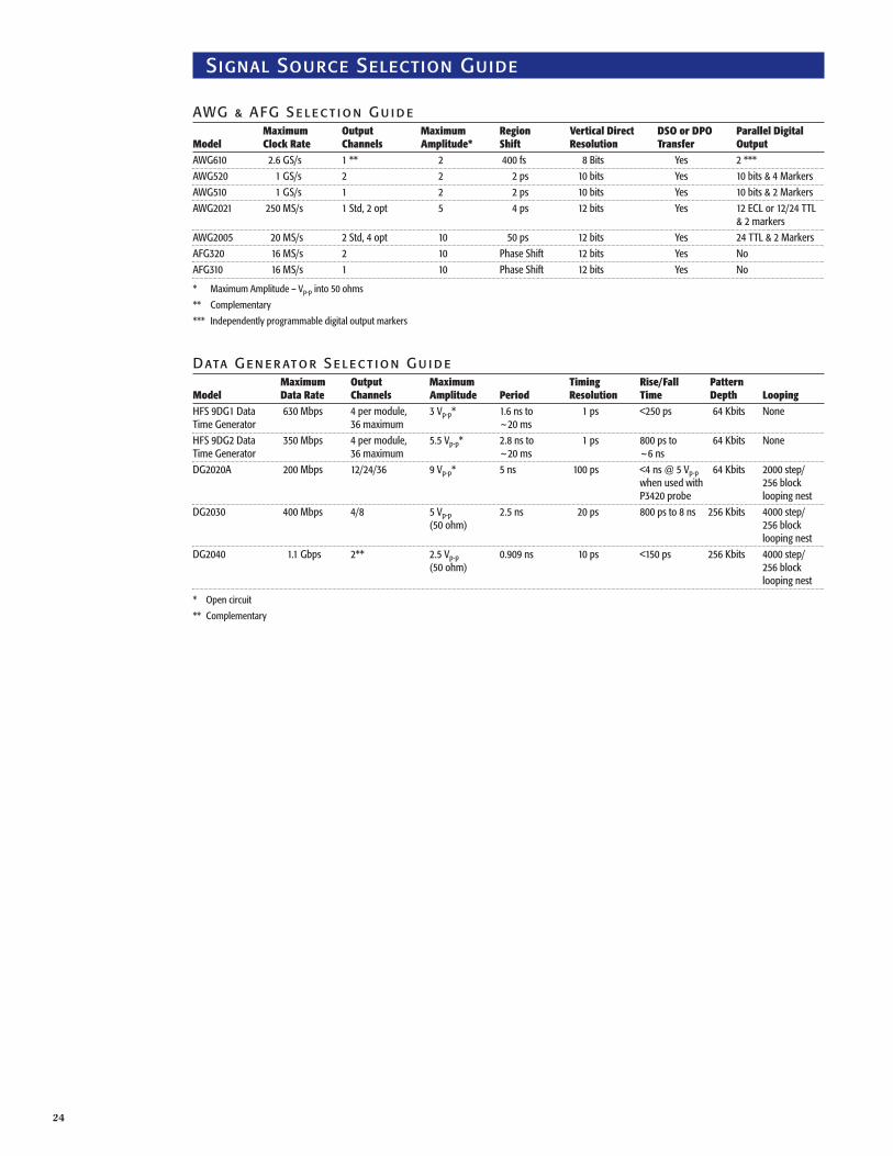
AWG & AFG Select ion GuideMaximum Output Maximum Region Vertical Direct DSO or DPO Parallel Digital
Model Clock Rate Channels Amplitude* Shift Resolution Transfer OutputAWG610 2.6 GS/s 1 ** 2 400 fs 8 Bits Yes 2 ***AWG520 1 GS/s 2 2 2 ps 10 bits Yes 10 bits & 4 MarkersAWG510 1 GS/s 1 2 2 ps 10 bits Yes 10 bits & 2 MarkersAWG2021 250 MS/s 1 Std, 2 opt 5 4 ps 12 bits Yes 12 ECL or 12/24 TTL
& 2 markersAWG2005 20 MS/s 2 Std, 4 opt 10 50 ps 12 bits Yes 24 TTL & 2 MarkersAFG320 16 MS/s 2 10 Phase Shift 12 bits Yes NoAFG310 16 MS/s 1 10 Phase Shift 12 bits Yes No
* Maximum Amplitude – Vp-p into 50 ohms
** Complementary
*** Independently programmable digital output markers
Data Generator Select ion GuideMaximum Output Maximum Timing Rise/Fall Pattern
Model Data Rate Channels Amplitude Period Resolution Time Depth LoopingHFS 9DG1 Data 630 Mbps 4 per module, 3 Vp-p* 1.6 ns to 1 ps <250 ps 64 Kbits NoneTime Generator 36 maximum ~20 msHFS 9DG2 Data 350 Mbps 4 per module, 5.5 Vp-p* 2.8 ns to 1 ps 800 ps to 64 Kbits NoneTime Generator 36 maximum ~20 ms ~6 nsDG2020A 200 Mbps 12/24/36 9 Vp-p* 5 ns 100 ps <4 ns @ 5 Vp-p 64 Kbits 2000 step/
when used with 256 block P3420 probe looping nest
DG2030 400 Mbps 4/8 5 Vp-p 2.5 ns 20 ps 800 ps to 8 ns 256 Kbits 4000 step/(50 ohm) 256 block
looping nestDG2040 1.1 Gbps 2** 2.5 Vp-p 0.909 ns 10 ps <150 ps 256 Kbits 4000 step/
(50 ohm) 256 block looping nest
* Open circuit
** Complementary
Signal Source Selection Guide


The Tektronix signal sources family is a key component of the powerful Tektronix instrument ensemble fortesting the most challenging mixed-signal design and manufacturing test applications.
This integrated tool set includes sampling oscilloscopes, digital storage oscilloscopes, digital phosphor oscillo-scopes, logic analyzers, and a host of complementary connection devices.
Characterize High-speed Digital SignalsMeasuring high-speed signal characteristics requires tools with uncompromised performance.The TDS694C Digital Storage Oscilloscope (DSO) has 3 GHz bandwidth and 10 GS/s samplerate across four channels simultaneously to ensure the most accurate single-shot rise-timeand timing measurements available. A special cross-triggering capability enables correlationwith TLA logic analyzers.
Analyze Complex SignalsAn affordable solution for many applications is the TDS3000 Series Digital PhosphorOscilloscope (DPO). This highly portable oscilloscope delivers up to 500 MHz bandwidth andsample rates up to 5 GS/s. Its intensity-graded color display helps you locate and characterizeanomalies that are often elusive on traditional Digital Storage Oscilloscopes.
Measure Circuit Board ImpedanceThe TDS8000 Digital Sampling Oscilloscope with the 80E04 TDR/Sampling module is anoutstanding solution for circuit board impedance measurements, featuring a reflected rise timeof <35 ps and 20 GHz bandwidth.
Examine Digital Systems in Real-TimeFor design teams who need to debug and verify their product designs, Tektronix LogicAnalyzers provide breakthrough features that capture, analyze, and display the real-timebehavior of digital systems operation. The TLA700 and TLA600 Series feature powerfulstate-based triggering plus the ability to simultaneously acquire 2 GHz timing data and200 MHz state data through the same probe. The TLA family operates with an openWindows® platform, allowing easy integration into the design environment.
Secure the Critical ConnectionEven the most advanced instrument can only be as precise as the data that goes into it.Tektronix is the leader in technologies that enable access to the device-under-test. Ourbroad selection of probes and interconnect accessories includes the world’s most advancedhigh-bandwidth active and differential probes which provide access to dense, high-speedcircuitry while maintaining maximum signal fidelity.
For further information, contact Tektronix:
Worldwide Web: for the most up-to-date product information visit our web site at: www.tektronix.com/measurement/signal_sources/ASEAN Countries (65) 356-3900; Australia & New Zealand 61 (2) 9888-0100; Austria, Central Eastern Europe, Greece, Turkey, Malta,& Cyprus +43 2236 8092 0; Belgium +32 (2) 715 89 70; Brazil and South America 55 (11) 3741-8360; Canada 1 (800) 661-5625; Denmark +45 (44) 850 700; Finland +358 (9) 4783 400; France & North Africa +33 1 69 86 81 81; Germany + 49 (221) 94 77 400; Hong Kong (852) 2585-6688; India (91) 80-2275577; Italy +39 (2) 25086 501; Japan (Sony/Tektronix Corporation) 81 (3) 3448-3111; Mexico, Central America, & Caribbean 52 (5) 666-6333; The Netherlands +31 23 56 95555; Norway +47 22 07 07 00;People’s Republic of China 86 (10) 6235 1230; Republic of Korea 82 (2) 528-5299; South Africa (27 11)651-5222; Spain & Portugal +34 91 372 6000;Sweden +46 8 477 65 00; Switzerland +41 (41) 729 36 40; Taiwan 886 (2) 2722-9622; United Kingdom & Eire +44 (0)1344 392000; USA 1 (800) 426-2200.
From other areas, contact: Tektronix, Inc. Export Sales, P.O. Box 500, M/S 50-255, Beaverton, Oregon 97077-0001, USA 1 (503) 627-6877.
0300 TD/XBS 76W-13740-0
Copyright © 2000, Tektronix, Inc. All rights reserved. Tektronix products are covered by U.S. and foreign patents, issued and pending. Information in this publication supersedes that in all previously published material. Specification and price change privileges reserved. TEKTRONIX and TEK are registered trademarks of Tektronix, Inc. All other trade names referenced are the service marks, trademarks or registered trademarks of their respective companies.
The Integrated Tool Set for Superior Measurement and Analysis