An Integrated Dynamic Voltage ... - ieeexplore.ieee.org
10
Abstract—Cost of various energy storage technologies is decreasing rapidly and the integration of these technologies into the power grid is becoming a reality with the advent of smart grid. Dynamic Voltage Restorer is one product which can provide improved voltage sag and swell compensation with energy storage integration. Ultra-capacitors (UCAP) have low energy density and high power density ideal characteristics for compensation of voltage sags and voltage swells which are both events which require high power for short spans of time. The novel contribution of this paper lies in integration of rechargeable UCAP based energy storage into the dynamic voltage restorer topology. With this integration the UCAP-DVR system will have active power capability and will be able to independently compensate temporary voltage sags and swells without relying on the grid to compensate for faults on the grid like in the past. UCAP is integrated into dc-link of the DVR through a bi- directional dc-dc converter which helps in providing a stiff dc-link voltage and the integrated UCAP-DVR system helps in compensating Temporary voltage sags and voltage swells which last from 3s-1min. Complexities involved in the design and control of both the dc-ac inverter and the dc-dc converter are discussed. The simulation model of the overall system is developed and compared to the experimental hardware setup. Index Terms- UCAP, DVR, dc-dc converter, DSP, sag/swell, d-q control, PLL, energy storage integration I. INTRODUCTION The concept of using inverter based Dynamic voltage restorers for preventing customers from momentary voltage disturbances on the utility side was demonstrated for the first time by Woodley etal [1]. The concept of using the dynamic voltage restorer (DVR) as a power quality product has gained significant popularity since its first use. In [1], the authors propose the usage of the DVR with rechargeable energy storage at the dc-terminal to meet the active power requirements of the grid during voltage disturbances. In order to avoid and minimize the active power injection into the grid the authors also mention an alternative solution which is to compensate for the voltage sag by inserting a lagging voltage in quadrature with the line current. Due to the high cost of rechargeable energy storage various other types of control strategies have also been developed in the literature [2-8] to minimize the active power injection from the DVR. The high cost of the rechargeable energy storage prevents the penetration of the dynamic voltage restorer as a power quality product. However, the cost of rechargeable energy storage has been decreasing drastically in the recent past due to various technological developments and due to higher penetration in the market in the form of auxiliary energy storage for distributed energy resources (DERs) like wind, solar, HEVs and PHEVs [9, 10]. Therefore, there has been renewed interest in the literature [10-17] to integrate re- chargeable energy storage again at the dc-terminal of power quality products like STATCOM and DVR. Various types of rechargeable energy storage technologies based on Superconducting magnets (SMES), flywheels (FESS), batteries (BESS) and Ultra-capacitors (UCAPs) are compared in [10] for integration into advanced power applications like DVR. Efforts have been made to integrate energy storage into the DVR system which will give the system active power capability which makes it independent of the grid during voltage disturbances. In [11] cascaded H- bridge based DVR with a thyristor controlled inductor is proposed in order to minimize the energy storage requirements. In [12] flywheel energy storage is integrated into the DVR system to improve its steady state series and shunt compensation. Of all the rechargeable energy storage technologies UCAPs are ideally suited for applications which need active power support in the milliseconds to seconds timescale [10], [13], [14]. Therefore, UCAP based integration into the DVR system is ideal as the normal duration of momentary voltage sags and swells is in the milliseconds to seconds range [15]. UCAPs have low energy density and high power density ideal characteristics for compensating voltage sags and An Integrated Dynamic Voltage Restorer - Ultracapacitor Design for Improving Power Quality of the Distribution Grid D. Somayajula, Student Member, IEEE, and M. L. Crow, Fellow, IEEE Digital Object Identifier 10.1109/TSTE.2015.2402221 1949-3029 © 2015 IEEE. Personal use is permitted, but republication/redistribution requires IEEE permission. See http://www.ieee.org/publications_standards/publications/rights/index.html for more information. http://ieeexplore.ieee.org/Xplore
Transcript of An Integrated Dynamic Voltage ... - ieeexplore.ieee.org

Abstract—Cost of various energy storage technologies is decreasing rapidly and the integration of these technologies into the power grid is becoming a reality with the advent of smart grid. Dynamic Voltage Restorer is one product which can provide improved voltage sag and swell compensation with energy storage integration. Ultra-capacitors (UCAP) have low energy density and high power density ideal characteristics for compensation of voltage sags and voltage swells which are both events which require high power for short spans of time. The novel contribution of this paper lies in integration of rechargeable UCAP based energy storage into the dynamic voltage restorer topology. With this integration the UCAP-DVR system will have active power capability and will be able to independently compensate temporary voltage sags and swells without relying on the grid to compensate for faults on the grid like in the past. UCAP is integrated into dc-link of the DVR through a bi-directional dc-dc converter which helps in providing a stiff dc-link voltage and the integrated UCAP-DVR system helps in compensating Temporary voltage sags and voltage swells which last from 3s-1min. Complexities involved in the design and control of both the dc-ac inverter and the dc-dc converter are discussed. The simulation model of the overall system is developed and compared to the experimental hardware setup.
Index Terms- UCAP, DVR, dc-dc converter, DSP, sag/swell, d-q control, PLL, energy storage integration
I. INTRODUCTION
The concept of using inverter based Dynamic voltage restorers for preventing customers from momentary voltage disturbances on the utility side was demonstrated for the first time by Woodley etal [1]. The concept of using the dynamic voltage restorer (DVR) as a power quality product has gained significant popularity since its first use. In [1], the authors propose the usage of the DVR with rechargeable energy storage at the dc-terminal to meet the active power
requirements of the grid during voltage disturbances. In order to avoid and minimize the active power injection into the grid the authors also mention an alternative solution which is to compensate for the voltage sag by inserting a lagging voltage in quadrature with the line current. Due to the high cost of rechargeable energy storage various other types of control strategies have also been developed in the literature [2-8] to minimize the active power injection from the DVR. The high cost of the rechargeable energy storage prevents the penetration of the dynamic voltage restorer as a power quality product. However, the cost of rechargeable energy storage has been decreasing drastically in the recent past due to various technological developments and due to higher penetration in the market in the form of auxiliary energy storage for distributed energy resources (DERs) like wind, solar, HEVs and PHEVs [9, 10]. Therefore, there has been renewed interest in the literature [10-17] to integrate re-chargeable energy storage again at the dc-terminal of power quality products like STATCOM and DVR.
Various types of rechargeable energy storage technologies based on Superconducting magnets (SMES), flywheels (FESS), batteries (BESS) and Ultra-capacitors (UCAPs) are compared in [10] for integration into advanced power applications like DVR. Efforts have been made to integrate energy storage into the DVR system which will give the system active power capability which makes it independent of the grid during voltage disturbances. In [11] cascaded H-bridge based DVR with a thyristor controlled inductor is proposed in order to minimize the energy storage requirements. In [12] flywheel energy storage is integrated into the DVR system to improve its steady state series and shunt compensation.
Of all the rechargeable energy storage technologies UCAPs are ideally suited for applications which need active power support in the milliseconds to seconds timescale [10], [13], [14]. Therefore, UCAP based integration into the DVR system is ideal as the normal duration of momentary voltage sags and swells is in the milliseconds to seconds range [15]. UCAPs have low energy density and high power density ideal characteristics for compensating voltage sags and
An Integrated Dynamic Voltage Restorer-Ultracapacitor Design for Improving Power
Quality of the Distribution Grid
D. Somayajula, Student Member, IEEE, and M. L. Crow, Fellow, IEEE
Digital Object Identifier 10.1109/TSTE.2015.2402221
1949-3029 © 2015 IEEE. Personal use is permitted, but republication/redistribution requires IEEE permission.See http://www.ieee.org/publications_standards/publications/rights/index.html for more information.
http://ieeexplore.ieee.org/Xplore
voltage swells which are both events which require high amount of power for short spans of time. UCAPs also have higher number of charge/discharge cycles when compared to batteries and for the same module size UCAPs have higher terminal voltage when compared to batteries which makes the integration easier. With the prevalence of renewable energy sources on the distribution grid and the corresponding increase in power quality problems the need for DVRs on the distribution grid is increasing [16]. Super-capacitor based energy storage integration into the DVR for the distribution grid is proposed in [16] and [17]. However, the concept is introduced only through simulation and experimental results are not presented. In the present paper UCAP based energy storage integration to a DVR into the distribution grid is proposed and the following application areas are addressed,
Integration of the UCAP with DVR system gives the system active power capability which is necessary for independently compensating voltage sags and swells
Experimental validation of the UCAP, dc-dc converter, inverter their interface and control
Development of inverter and dc-dc converter controls to provide Sag and Swell compensation to the distribution grid
Hardware integration and performance validation of the integrated DVR-UCAP system
II. THREE-PHASE SERIES INVERTER
A. Power Stage
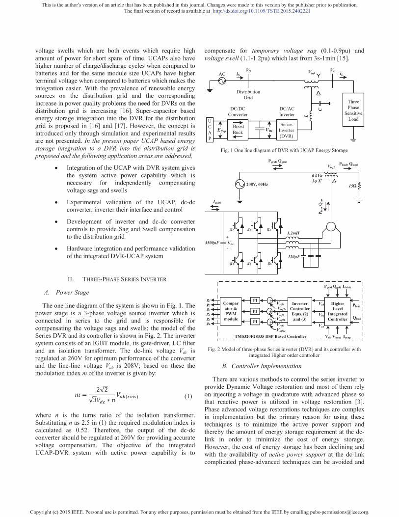
The one line diagram of the system is shown in Fig. 1. The power stage is a 3-phase voltage source inverter which is connected in series to the grid and is responsible for compensating the voltage sags and swells; the model of the Series DVR and its controller is shown in Fig. 2. The inverter system consists of an IGBT module, its gate-driver, LC filter and an isolation transformer. The dc-link voltage Vdc is regulated at 260V for optimum performance of the converter and the line-line voltage Vab is 208V; based on these the modulation index m of the inverter is given by:
(1)
where n is the turns ratio of the isolation transformer. Substituting n as 2.5 in (1) the required modulation index is calculated as 0.52. Therefore, the output of the dc-dc converter should be regulated at 260V for providing accurate voltage compensation. The objective of the integrated UCAP-DVR system with active power capability is to
compensate for temporary voltage sag (0.1-0.9pu) and voltage swell (1.1-1.2pu) which last from 3s-1min [15].
Fig. 1 One line diagram of DVR with UCAP Energy Storage
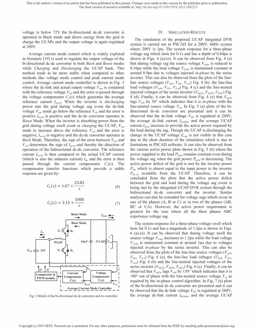
Fig. 2 Model of three-phase Series inverter (DVR) and its controller with
integrated Higher order controller
B. Controller Implementation
There are various methods to control the series inverter to provide Dynamic Voltage restoration and most of them rely on injecting a voltage in quadrature with advanced phase so that reactive power is utilized in voltage restoration [3]. Phase advanced voltage restorations techniques are complex in implementation but the primary reason for using these techniques is to minimize the active power support and thereby the amount of energy storage requirement at the dc-link in order to minimize the cost of energy storage. However, the cost of energy storage has been declining and with the availability of active power support at the dc-link complicated phase-advanced techniques can be avoided and
AC iLiS
UCAP
ThreePhase
SensitiveLoad
SeriesInverter(DVR)
DC/DCConverter
VS
VDC
Vinj
DC/ACInverter
VL
BoostBuckECap
L
C
DistributionGrid
3500μF
1.2mH
120μF
g1 g2
g3
g4
g5 g6
208V, 60Hz
Pgrid, Qgrid
P inv
,Qin
v
Pload, Qload
InverterControllerEqns. (2)and (3)
g1
g6
g3g4g5
g2 Vrefa
Vrefb
Vrefc
Comparator &PWM
module
Vinj2a
+-
+
+-
-
PI
PI
PI
15
6 kVa3 Xr
Idclnk
Vdc
+
-
TMS320F28335 DSP Based Controller
Vinj2b
Vinj2c
Vinj2
Vab
Vbc
Vca
HigherLevel
IntegratedController
Pgrid Qgrid
Vdc Vucap
Pload
Qload
Iucap
Idclnk
This is the author's version of an article that has been published in this journal. Changes were made to this version by the publisher prior to publication.The final version of record is available at http://dx.doi.org/10.1109/TSTE.2015.2402221
Copyright (c) 2015 IEEE. Personal use is permitted. For any other purposes, permission must be obtained from the IEEE by emailing [email protected].

voltages can be injected in-phase with the system voltage during a voltage sag or a swell event. The control method requires the use of a PLL to find the rotating angle . As discussed previously the goal of this project is to use the active power capability of the UCAP-DVR system and compensate temporary voltage sags and swells.
The inverter controller implementation is based on injecting voltages in-phase with the supply side line-neutral voltages. This requires PLL for estimating which has been implemented using the fictitious power method described in [18]. Based on the estimated and the line-line source voltages Vab, Vbc, Vca (which are available for this delta-sourced system) are transformed into the d-q domain and the line-neutral components of the source voltage Vsa, Vsb and Vsc which are not available can then be estimated using:
(2)
(3)
(4)
These voltages are normalized to unit sine waves using line-neutral system voltage of 120Vrms as reference and compared to unit sine waves in-phase with actual system voltages Vs from (3) to find the injected voltage references Vref necessary to maintain a constant voltage at the load terminals where m is 0.52 from (1). Therefore, whenever there is a voltage sag or swell on the source side a corresponding voltage Vinj2 is injected in-phase by the DVR and UCAP system to negate the effect and retain a constant voltage VL at the load end. The actual active and reactive power supplied by the series inverter can be computed using (4) from the RMS values of injected voltage Vinj2a and load current ILa and is the phase difference between the two waveforms.
III. UCAP AND BI-DIRECTIONAL DC-DC CONVERTER
A. UCAP Bank Hardware Setup
The choice of the number of UCAPs necessary for providing grid support depends on the amount of support
needed, terminal voltage of the UCAP, dc-link voltage and distribution grid voltages. In this paper the experimental setup consists of three 48V, 165F UCAPs (BMOD0165P048) manufactured by Maxwell Technologies which are connected in series. Therefore, the terminal voltage of the UCAP bank is 144V and the dc-link voltage is programmed to 260V this would give the dc-dc converter a practical operating duty ratio of 0. to 0. 2 in the “Boost mode” while the UCAP is discharging and 0.2 to 0. in the “Buck mode” while the UCAP is charging from the grid through the dc-link and the dc-dc converter. It is practical and cost effective to use 3 modules in the UCAP bank. Assuming that the UCAP bank can be discharged to 50% of its initial voltage (Vuc,ini) to final voltage (Vuc,fin) from 144V to 72V which translates to depth of discharge of 75%, the energy in the UCAP bank available for discharge is given by:
(5)
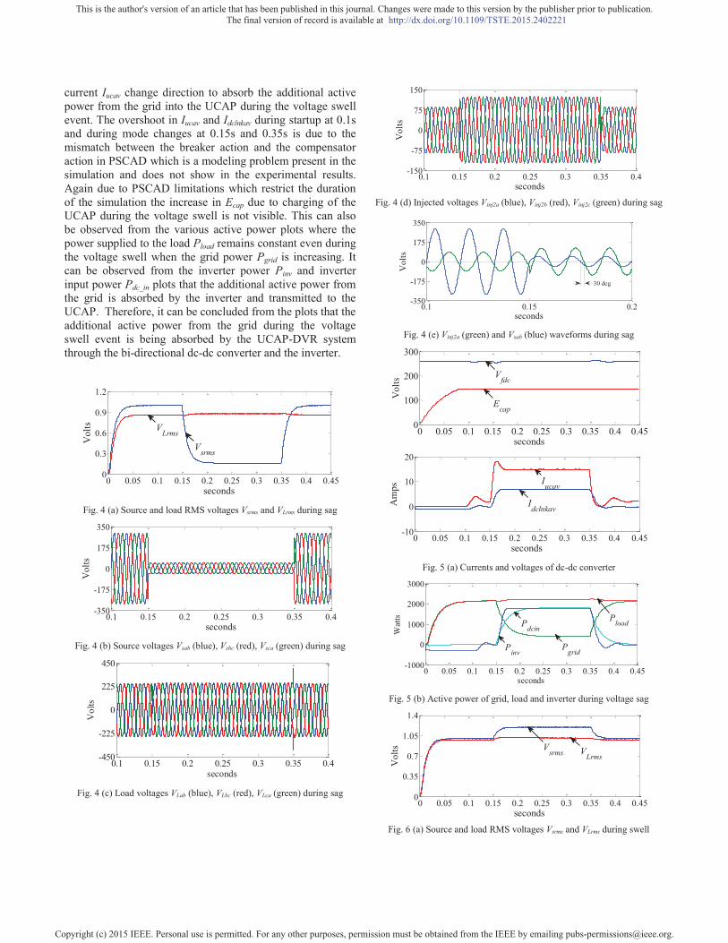
B. Bi-directional dc-dc converter and Controller
A UCAP cannot be directly connected to the dc-link of the inverter like a battery as the voltage profile of the UCAP varies as it discharges energy. Therefore, there is a need to integrate the UCAP system through a bi-directional dc-dc converter which maintains a stiff dc-link voltage as the UCAP voltage decreases while “Discharging” and increases while “Charging”. he model of the bi-directional dc-dc converter and its controller are shown in Fig. 3 where the input consists of 3 UCAPs connected in series and the output consists of a nominal load of 2 . to prevent operation at no-load and the output is connected to the dc-link of the inverter. The amount of active power support required by the grid during a voltage sag event is dependent on the depth and duration of the voltage sag and the dc-dc converter should be able to withstand this power during “Discharge” mode. The dc-dc converter should also be able to operate in bi-directional mode to be able to “Charge” or absorb additional power from the grid during voltage swell event. In this paper the bi-directional dc-dc converter acts as a boost converter while “discharging” power from the UCAP and acts as a buck converter while “charging” the UCAP from the grid.
A bi-directional dc-dc converter is required as an interface between the UCAP and the dc-link since the UCAP voltage varies with the amount of energy discharged while the dc-link voltage has to be stiff. Therefore, bi-directional dc-dc converter is designed to operate in boost mode when the UCAP bank voltage is between 72V to 144V and the output voltage is regulated at 260V. And when the UCAP bank
This is the author's version of an article that has been published in this journal. Changes were made to this version by the publisher prior to publication.The final version of record is available at http://dx.doi.org/10.1109/TSTE.2015.2402221
Copyright (c) 2015 IEEE. Personal use is permitted. For any other purposes, permission must be obtained from the IEEE by emailing [email protected].
voltage is below 72V the bi-directional dc-dc converter is operated in Buck mode and draws energy from the grid to charge the UCAPs and the output voltage is again regulated at 260V.
Average current mode control which is widely explored in literature [19] is used to regulate the output voltage of the bi-directional dc-dc converter in both Buck and Boost modes while Charging and Discharging the UCAP bank. This method tends to be more stable when compared to other methods like voltage mode control and peak current mode control. Average current mode controller is shown in Fig. 3 where the dc-link and actual output voltage Vout is compared with the reference voltage Vref and the error is passed through the voltage compensator C1(s) which generates the average reference current Iucref. When the inverter is discharging power into the grid during voltage sag event the dc-link voltage Vout tends go below the reference Vref and the error is positive Iucref is positive and the dc-dc converter operates in Boost Mode. When the inverter is absorbing power from the grid during voltage swell event or charging the UCAP, Vout tends to increase above the reference Vref and the error is negative, Iucref is negative and the dc-dc converter operates in Buck Mode. Therefore, the sign of the error between Vout and Vref determines the sign of Iucref and thereby the direction of operation of the bidirectional dc-dc converter. The reference current Iucref is then compared to the actual UCAP current (which is also the inductor current) Iuc and the error is then passed through the current compensator C2(s). The compensator transfer functions which provide a stable response are given by:
(6)
(7)
Fig. 3 Model of the bi-directional dc-dc converter and its controller
IV. SIMULATION RESULTS
The simulation of the proposed UCAP integrated DVR system is carried out in PSCAD for a 208V, 60Hz system where 208V is 1pu. The system response for a three-phase voltage sag which lasts for 0.1s and has a depth of 0.84pu is shown in Figs. 4 (a)-(e). It can be observed from Fig. 4 (a) that during voltage sag the source voltage Vsrms is reduced to 0.16pu while the load voltage VLrms is maintained constant at around 0.9pu due to voltages injected in-phase by the series inverter. This can also be observed from the plots of the line-line source voltages (Vsab, Vsbc, Vsca) Fig. 4 (b), the line-line load voltages (VLab, VLbc, VLca) Fig. 4 (c) and the line-neutral injected voltages of the series inverter (Vinj2a, Vinj2b, Vinj2c) Fig. 4 (d). Finally, it can be observed from Fig. 4 (e) that Vinj2a lags Vsab by 30° which indicates that it is in-phase with the line-neutral source voltage Vsa. In Fig. 5 (a) plots of the bi-directional dc-dc converter are presented and it can be observed that the dc-link voltage Vfdc is regulated at 260V, the average dc-link current Idclnkav and the average UCAP current Iucav increase to provide the active power required by the load during the sag. Though the UCAP is discharging the change in the UCAP voltage Ecap is not visible in this case due to the short duration of the simulation which is due to limitations in PSCAD software. It can also be observed from the various active power plots shown in Fig. 5 (b) where the power supplied to the load Pload remains constant even during the voltage sag when the grid power Pgrid is decreasing. The active power deficit of the grid is met by the inverter power Pinv which is almost equal to the input power to the inverter Pdc_in available from the UCAP. Therefore, it can be concluded from the plots that the active power deficit between the grid and load during the voltage sag event is being met by the integrated UCAP-DVR system through the bidirectional dc-dc converter and the inverter. Similar analysis can also be extended for voltage sags which occur in one of the phases (A, B or C) or in two of the phases (AB, BC or CA). However, the active power requirement is greatest for the case where all the three phases ABC experience voltage sag.
The system response for a three-phase voltage swell which lasts for 0.1s and has a magnitude of 1.2pu is shown in Figs. 6 (a)-(e). It can be observed that during voltage swell the source voltage Vsrms increases to 1.2pu while the load voltage VLrms is maintained constant at around 1pu due to voltages injected in-phase by the series inverter. This can also be observed from the plots of the line-line source voltages (Vsab, Vsbc, Vsca) Fig. 6 (a), the line-line load voltages (VLab, VLbc, VLca) Fig. 6 (b) and the line-neutral injected voltages of the series inverter (Vinj2a, Vinj2b, Vinj2c) Fig. 6 (c). Finally, it can be observed that Vinj2a lags Vsab by 150° which indicates that it is 180° out of phase with the line-neutral source voltage Vsa as required by the in-phase control algorithm. In Fig. 7 (a) plots of the bi-directional dc-dc converter are presented and it can be observed that the dc-link voltage Vfdc is regulated at 260V, the average dc-link current Idclnkav and the average UCAP
D1Ecap
D2
181μH 44μF 213.5
S1
S2Iuc
Vout
-
+
VrefIucref
Iuc
Idclnk
S1
Buck Mode
Boost Mode
Average Current Mode Controller
+
-
+
-
55F
CurrentCompensator
C2(s)
VoltageCompensator
C1(s)
Comparator &PWM module
S2
This is the author's version of an article that has been published in this journal. Changes were made to this version by the publisher prior to publication.The final version of record is available at http://dx.doi.org/10.1109/TSTE.2015.2402221
Copyright (c) 2015 IEEE. Personal use is permitted. For any other purposes, permission must be obtained from the IEEE by emailing [email protected].
current Iucav change direction to absorb the additional active power from the grid into the UCAP during the voltage swell event. The overshoot in Iucav and Idclnkav during startup at 0.1s and during mode changes at 0.15s and 0.35s is due to the mismatch between the breaker action and the compensator action in PSCAD which is a modeling problem present in the simulation and does not show in the experimental results. Again due to PSCAD limitations which restrict the duration of the simulation the increase in Ecap due to charging of the UCAP during the voltage swell is not visible. This can also be observed from the various active power plots where the power supplied to the load Pload remains constant even during the voltage swell when the grid power Pgrid is increasing. It can be observed from the inverter power Pinv and inverter input power Pdc_in plots that the additional active power from the grid is absorbed by the inverter and transmitted to the UCAP. Therefore, it can be concluded from the plots that the additional active power from the grid during the voltage swell event is being absorbed by the UCAP-DVR system through the bi-directional dc-dc converter and the inverter.
Fig. 4 (a) Source and load RMS voltages Vsrms and VLrms during sag
Fig. 4 (b) Source voltages Vsab (blue), Vsbc (red), Vsca (green) during sag
Fig. 4 (c) Load voltages VLab (blue), VLbc (red), VLca (green) during sag
Fig. 4 (d) Injected voltages Vinj2a (blue), Vinj2b (red), Vinj2c (green) during sag
Fig. 4 (e) Vinj2a (green) and Vsab (blue) waveforms during sag
Fig. 5 (a) Currents and voltages of dc-dc converter
Fig. 5 (b) Active power of grid, load and inverter during voltage sag
Fig. 6 (a) Source and load RMS voltages Vsrms and VLrms during swell
0 0.05 0.1 0.15 0.2 0.25 0.3 0.35 0.4 0.450
0.3
0.6
0.9
1.2
seconds
Vol
ts
0.1 0.15 0.2 0.25 0.3 0.35 0.4-350
-175
0
175
350
seconds
Vol
ts
0.1 0.15 0.2 0.25 0.3 0.35 0.4-450
-225
0
225
450
seconds
Vol
ts
0.1 0.15 0.2 0.25 0.3 0.35 0.4-150
-75
0
75
150
seconds
Vol
ts
0.1 0.15 0.2-350
-175
0
175
350
seconds
Vol
ts
30 deg
0 0.05 0.1 0.15 0.2 0.25 0.3 0.35 0.4 0.450
100
200
300
seconds
Vol
ts
0 0.05 0.1 0.15 0.2 0.25 0.3 0.35 0.4 0.45-10
0
10
20
seconds
Am
ps
0 0.05 0.1 0.15 0.2 0.25 0.3 0.35 0.4 0.45-1000
0
1000
2000
3000
seconds
Wat
ts
0 0.05 0.1 0.15 0.2 0.25 0.3 0.35 0.4 0.450
0.35
0.7
1.05
1.4
seconds
Vol
ts
This is the author's version of an article that has been published in this journal. Changes were made to this version by the publisher prior to publication.The final version of record is available at http://dx.doi.org/10.1109/TSTE.2015.2402221
Copyright (c) 2015 IEEE. Personal use is permitted. For any other purposes, permission must be obtained from the IEEE by emailing [email protected].
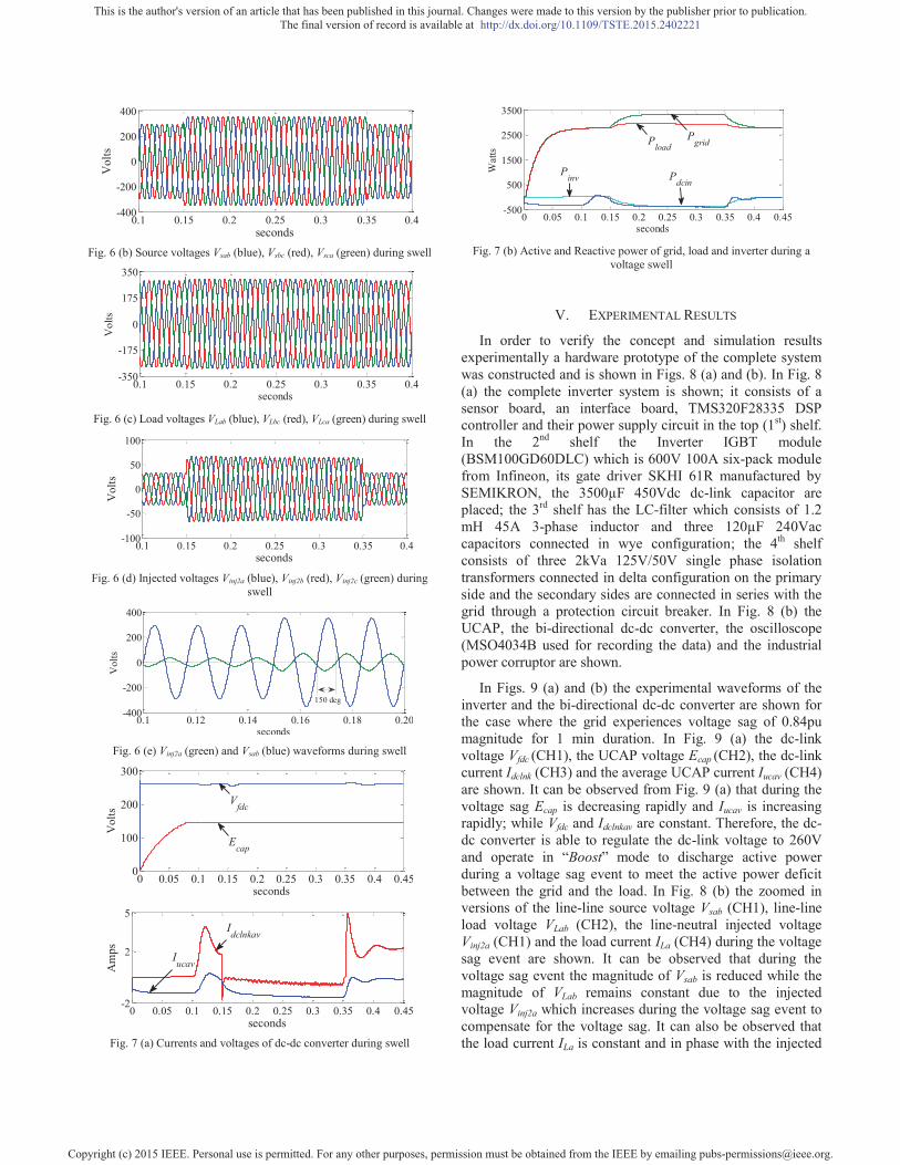
Fig. 6 (b) Source voltages Vsab (blue), Vsbc (red), Vsca (green) during swell
Fig. 6 (c) Load voltages VLab (blue), VLbc (red), VLca (green) during swell
Fig. 6 (d) Injected voltages Vinj2a (blue), Vinj2b (red), Vinj2c (green) during
swell
Fig. 6 (e) Vinj2a (green) and Vsab (blue) waveforms during swell
Fig. 7 (a) Currents and voltages of dc-dc converter during swell
Fig. 7 (b) Active and Reactive power of grid, load and inverter during a
voltage swell
V. EXPERIMENTAL RESULTS
In order to verify the concept and simulation results experimentally a hardware prototype of the complete system was constructed and is shown in Figs. 8 (a) and (b). In Fig. 8 (a) the complete inverter system is shown; it consists of a sensor board, an interface board, TMS320F28335 DSP controller and their power supply circuit in the top (1st) shelf. In the 2nd shelf the Inverter IGBT module (BSM100GD60DLC) which is 600V 100A six-pack module from Infineon, its gate driver SKHI 61R manufactured by SEMIKRON, the 3500μF 450Vdc dc-link capacitor are placed; the 3rd shelf has the LC-filter which consists of 1.2 mH 45A 3-phase inductor and three 120μF 240Vac capacitors connected in wye configuration; the 4th shelf consists of three 2kVa 125V/50V single phase isolation transformers connected in delta configuration on the primary side and the secondary sides are connected in series with the grid through a protection circuit breaker. In Fig. 8 (b) the UCAP, the bi-directional dc-dc converter, the oscilloscope (MSO4034B used for recording the data) and the industrial power corruptor are shown.
In Figs. 9 (a) and (b) the experimental waveforms of the inverter and the bi-directional dc-dc converter are shown for the case where the grid experiences voltage sag of 0.84pu magnitude for 1 min duration. In Fig. 9 (a) the dc-link voltage Vfdc (CH1), the UCAP voltage Ecap (CH2), the dc-link current Idclnk (CH3) and the average UCAP current Iucav (CH4) are shown. It can be observed from Fig. 9 (a) that during the voltage sag Ecap is decreasing rapidly and Iucav is increasing rapidly; while Vfdc and Idclnkav are constant. Therefore, the dc-dc converter is able to regulate the dc-link voltage to 260V and operate in “Boost” mode to discharge active power during a voltage sag event to meet the active power deficit between the grid and the load. In Fig. 8 (b) the zoomed in versions of the line-line source voltage Vsab (CH1), line-line load voltage VLab (CH2), the line-neutral injected voltage Vinj2a (CH1) and the load current ILa (CH4) during the voltage sag event are shown. It can be observed that during the voltage sag event the magnitude of Vsab is reduced while the magnitude of VLab remains constant due to the injected voltage Vinj2a which increases during the voltage sag event to compensate for the voltage sag. It can also be observed that the load current ILa is constant and in phase with the injected
0.1 0.15 0.2 0.25 0.3 0.35 0.4-400
-200
0
200
400
seconds
Vol
ts
0.1 0.15 0.2 0.25 0.3 0.35 0.4-350
-175
0
175
350
seconds
Vol
ts
0.1 0.15 0.2 0.25 0.3 0.35 0.4-100
-50
0
50
100
seconds
Vol
ts
0.1 0.12 0.14 0.16 0.18 0.20-400
-200
0
200
400
seconds
Vol
ts
150 deg
0 0.05 0.1 0.15 0.2 0.25 0.3 0.35 0.4 0.450
100
200
300
seconds
Vol
ts
0 0.05 0.1 0.15 0.2 0.25 0.3 0.35 0.4 0.45-2
2
5
seconds
Am
ps
0 0.05 0.1 0.15 0.2 0.25 0.3 0.35 0.4 0.45-500
500
1500
2500
3500
seconds
Wat
ts
This is the author's version of an article that has been published in this journal. Changes were made to this version by the publisher prior to publication.The final version of record is available at http://dx.doi.org/10.1109/TSTE.2015.2402221
Copyright (c) 2015 IEEE. Personal use is permitted. For any other purposes, permission must be obtained from the IEEE by emailing [email protected].
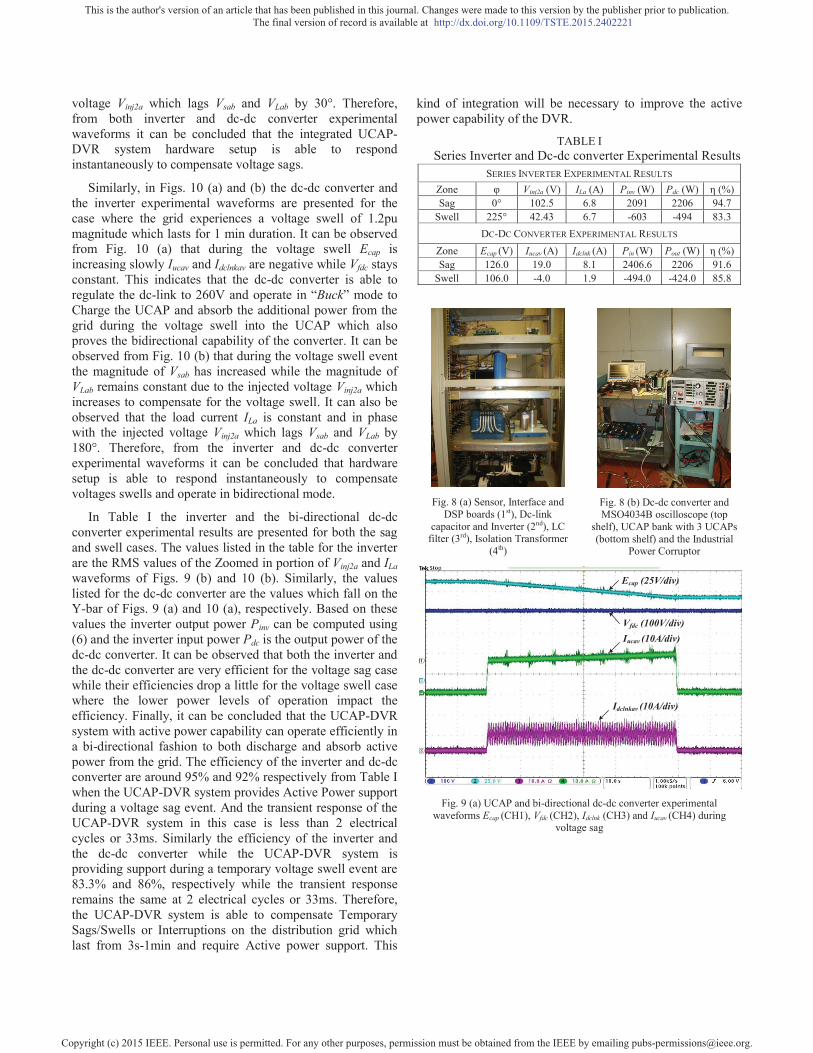
voltage Vinj2a which lags Vsab and VLab by 30°. Therefore, from both inverter and dc-dc converter experimental waveforms it can be concluded that the integrated UCAP-DVR system hardware setup is able to respond instantaneously to compensate voltage sags.
Similarly, in Figs. 10 (a) and (b) the dc-dc converter and the inverter experimental waveforms are presented for the case where the grid experiences a voltage swell of 1.2pu magnitude which lasts for 1 min duration. It can be observed from Fig. 10 (a) that during the voltage swell Ecap is increasing slowly Iucav and Idclnkav are negative while Vfdc stays constant. This indicates that the dc-dc converter is able to regulate the dc-link to 260V and operate in “Buck” mode to Charge the UCAP and absorb the additional power from the grid during the voltage swell into the UCAP which also proves the bidirectional capability of the converter. It can be observed from Fig. 10 (b) that during the voltage swell event the magnitude of Vsab has increased while the magnitude of VLab remains constant due to the injected voltage Vinj2a which increases to compensate for the voltage swell. It can also be observed that the load current ILa is constant and in phase with the injected voltage Vinj2a which lags Vsab and VLab by 180°. Therefore, from the inverter and dc-dc converter experimental waveforms it can be concluded that hardware setup is able to respond instantaneously to compensate voltages swells and operate in bidirectional mode.
In Table I the inverter and the bi-directional dc-dc converter experimental results are presented for both the sag and swell cases. The values listed in the table for the inverter are the RMS values of the Zoomed in portion of Vinj2a and ILa waveforms of Figs. 9 (b) and 10 (b). Similarly, the values listed for the dc-dc converter are the values which fall on the Y-bar of Figs. 9 (a) and 10 (a), respectively. Based on these values the inverter output power Pinv can be computed using (6) and the inverter input power Pdc is the output power of the dc-dc converter. It can be observed that both the inverter and the dc-dc converter are very efficient for the voltage sag case while their efficiencies drop a little for the voltage swell case where the lower power levels of operation impact the efficiency. Finally, it can be concluded that the UCAP-DVR system with active power capability can operate efficiently in a bi-directional fashion to both discharge and absorb active power from the grid. The efficiency of the inverter and dc-dc converter are around 95% and 92% respectively from Table I when the UCAP-DVR system provides Active Power support during a voltage sag event. And the transient response of the UCAP-DVR system in this case is less than 2 electrical cycles or 33ms. Similarly the efficiency of the inverter and the dc-dc converter while the UCAP-DVR system is providing support during a temporary voltage swell event are 83.3% and 86%, respectively while the transient response remains the same at 2 electrical cycles or 33ms. Therefore, the UCAP-DVR system is able to compensate Temporary Sags/Swells or Interruptions on the distribution grid which last from 3s-1min and require Active power support. This
kind of integration will be necessary to improve the active power capability of the DVR.
TABLE I Series Inverter and Dc-dc converter Experimental Results
SERIES INVERTER EXPERIMENTAL RESULTS Zone Vinj2a (V) ILa (A) Pinv (W) Pdc (W) (%) Sag 0° 102.5 6.8 2091 2206 94.7
Swell 225° 42.43 6.7 -603 -494 83.3 DC-DC CONVERTER EXPERIMENTAL RESULTS
Zone Ecap (V) Iucav (A) Idclnk (A) Pin (W) Pout (W) (%) Sag 126.0 19.0 8.1 2406.6 2206 91.6
Swell 106.0 -4.0 1.9 -494.0 -424.0 85.8
Fig. 8 (a) Sensor, Interface and
DSP boards (1st), Dc-link capacitor and Inverter (2nd), LC
filter (3rd), Isolation Transformer (4th)
Fig. 8 (b) Dc-dc converter and MSO4034B oscilloscope (top
shelf), UCAP bank with 3 UCAPs (bottom shelf) and the Industrial
Power Corruptor
Fig. 9 (a) UCAP and bi-directional dc-dc converter experimental
waveforms Ecap (CH1), Vfdc (CH2), Idclnk (CH3) and Iucav (CH4) during voltage sag
Vfdc (100V/div)
Ecap (25V/div)
Iucav (10A/div)
Idclnkav (10A/div)
This is the author's version of an article that has been published in this journal. Changes were made to this version by the publisher prior to publication.The final version of record is available at http://dx.doi.org/10.1109/TSTE.2015.2402221
Copyright (c) 2015 IEEE. Personal use is permitted. For any other purposes, permission must be obtained from the IEEE by emailing [email protected].

Fig. 9 (b) Inverter experimental waveforms Vsab (CH1), VLab (CH2) and Vinj2a
(CH3) and ILa (CH4) during the voltage sag
Fig. 10 (a) UCAP and dc-dc converter experimental waveforms Ecap (CH1),
Vfdc (CH2), Idclnk (CH3) and Iucav (CH4) during voltage swell
Fig. 10 (b) Inverter experimental waveforms Vsab (CH1), VLab (CH2) and
Vinj2a (CH3) and ILa (CH4) during the voltage swell
In Figs. 11 (a) and (b) the UCAP-PC system performance when the system experiences unbalanced voltage sag are presented. It can be observed from Fig. 11 (a) that a 20% voltage sag is generated in phases a and b the system
voltages Vsa and Vsb experience a voltage sag. However, the load current ILa remains constant because of the active power support to the sensitive load from the UCAP-DVR system even after the grid experiences unbalanced voltage sag. This clearly indicates that the PLL tracks the fundamental component even during unbalanced scenarios which allows the UCAP-APF system to provide active and reactive power support to the grid under unbalanced conditions. From the bi-directional dc-dc converter waveforms shown in Fig. 11 (b) it can be observed that during the unbalanced voltage sag which lasts for 1 second the dc-link voltage Vfdc has slight fluctuations and settles down to steady state value of 260V in less than 2 electrical cycles or 33ms.
Fig. 11 (a) Inverter experimental waveforms VLab (CH1), Vsa (CH2), Vsb
(CH3) and ILa (CH4) for during an unbalanced sag in phases a and b
Fig. 11 (b) Bi-directional dc-dc converter waveforms Ecap (CH1), Vfdc (CH2), Idclnk (CH3) and Iucav (CH4) showing transient response during an unbalanced
sag in phases a and b
VI. CONCLUSION
In this paper, the concept of integrating UCAP based rechargeable energy storage to the DVR system to improve its voltage restoration capabilities is explored. With this integration the DVR will be able to independently
Vsab (250V/div)
VLab (250V/div)
Vinj2a (100V/div)
ILa (10A/div)
Vfdc (100V/div)
Ecap (25V/div)
Iucav (2A/div)
Idclnkav (2A/div)
Vsab (250V/div)
VLab (250V/div)
Vinj2a (100V/div)
ILa (10A/div)
VLab (250V/div)
Vsa (250V/div)
Vsb (250V/div)
ILa (10A/div) 7.5Arms
Unbalanced voltage sag
10ms/div
Vfdc (100V/div)
Ecap (50V/div)
Iucav (10A/div)
Idclnkav (10A/div)
1sec
Unbalanced Voltage Sag
400ms/div
This is the author's version of an article that has been published in this journal. Changes were made to this version by the publisher prior to publication.The final version of record is available at http://dx.doi.org/10.1109/TSTE.2015.2402221
Copyright (c) 2015 IEEE. Personal use is permitted. For any other purposes, permission must be obtained from the IEEE by emailing [email protected].

compensate voltage sags and swells without relying on the grid to compensate for faults on the grid. The UCAP integration through a bi-directional dc-dc converter at the dc-link of the DVR is proposed. The power stage and control strategy of the series inverter which acts as the DVR are discussed. The control strategy is simple and is based on injecting voltages in-phase with the system voltage and is easier to implement when the DVR system has the ability to provide active power. A Higher level integrated controller which takes decisions based on the system parameters provides inputs to the inverter and dc-dc converter controllers to carry out their control actions. Designs of major components in the power stage of the bi-directional dc-dc converter are discussed. Average current mode control is used to regulate the output voltage of the dc-dc converter due to its inherently stable characteristic. The simulation of the UCAP-DVR system which consists of the UCAP, dc-dc converter, and the grid-tied inverter is carried out using PSCAD. Hardware experimental setup of the integrated system is presented and the ability to provide Temporary Voltage Sag and Swell compensation in all three phases to the distribution grid dynamically is tested. Results for transient response during voltage sags/swells in two phases will be included in the full-version of the paper. Results from simulation and experiment agree well with each other thereby verifying the concepts introduced in this paper. Similar UCAP based energy storages can be deployed in the future on the distribution grid to respond to dynamic changes in the voltage profiles of the grid and prevent sensitive loads from voltage disturbances.
VII. ACKNOWLEDGMENT The authors gratefully acknowledge the support received
from Department of Energy’s Sunshot initiative program DE-0006341 which aided in conducting this research.
REFERENCES [1] N. H. Woodley, L. Morgan and A. Sundaram, “Experience with an
inverter-based dynamic voltage restorer,” IEEE Trans. on Power Delivery, vol. 14, no. 3, pp. 1181-1186, Jul. 1999.
[2] S. S. Choi, B. H. Li and D. M. Vilathgamuwa, “Dynamic voltage restoration with minimum energy injection,” IEEE Trans. on Power Systems, vol. 15, no. 1, pp. 51-57, Feb. 2000.
[3] D. M. Vilathgamuwa, A. A. D. R. Perera, and S. S. Choi, “Voltage sag compensation with energy optimized dynamic voltage restorer,” IEEE Trans. on Power Delivery, vol. 18, no. 3, pp. 928-936, Jul. 2003.
[4] Y. W. Li, D. M. Vilathgamuwa, F. Blaabjerg and P. C. Loh “A robust control scheme for medium-voltage-level DVR implementation,” IEEE Trans. on Ind. Electron, vol. 54, no. 4, pp. 2249-2261, Aug. 2007.
[5] A. Ghosh and G. Ledwich, “Compensation of distribution system voltage using DVR,” IEEE Trans. on Power Delivery, vol. 17, no. 4, Oct. 2002.
[6] A. Elnady and M. M. A. Salama, “Mitigation of voltage disturbances using adaptive perceptron-based control algorithm,” IEEE Trans. on Power Delivery, vol. 20, no. 1, pp. 309-318, Jan. 2005.
[7] P. R. Sanchez, E. Acha, J. E. O. Calderon, V. Feliu and A. G. Cerrada, “A versatile control scheme for a dynamic voltage restorer for power quality improvement,” IEEE Trans. on Power Delivery, vol. 24, no. 1, pp. 277-284, Jan. 2009.
[8] C. S. Lam, M. C. Wong, and Y. D. Han, “Voltage swell and overvoltage compensation with unidirectional power flow controlled dynamic voltage restorer,” IEEE Trans. on Power Delivery, vol. 23, no .4, pp. 2513-2521, Oct. 2008.
[9] K. Sahay and B. Dwivedi, “Supercapacitor energy storage system for power quality improvement: An overview,” Journal of Energy Sources, pp. 1-8, 2009.
[10] P. F. Ribeiro, B. K. Johnson, M. L. Crow, A. Arsoy and Y. Liu, “Energy storage systems for advanced power applications,” Proc. IEEE, vol. 89, no. 12, pp. 1744-1756, Dec. 2001.
[11] H. K. Al-Hadidi, A. M. Gole and D. A. Jacobson, “A novel configuration for a cascaded inverter-based dynamic voltage restorer with reduced energy storage requirements,” IEEE Trans. on Power Delivery, vol. 23, no. 2, pp. 881-888, Apr. 2008.
[12] R. S. Weissbach, G. G. Karady, and R. G. Farmer, “Dynamic voltage compensation on distribution feeders using flywheel energy storage,” IEEE Trans. on Power Delivery, vol. 14, pp. 465–471, Apr. 1999.
[13] A. B. Arsoy, Y. Liu, P. F. Ribeiro and F. Wang, “StatCom-SMES,” IEEE Ind. Appl. Mag., vol. 9, no. 2, pp. 21-28, Mar. 2003.
[14] C. Abbey and G. Joos, “Supercapacitor energy storage for wind applications,” IEEE Trans. on Ind. Appl., vol. 43, no. 3, pp. 769-776, Jun. 2007.
[15] S. Santoso, M. F. McGranaghan, R. C. Dugan and H. W. Beaty, Electrical Power Systems Quality, 3rd ed. McGraw-Hill Professional, Jan. 2012.
[16] Y. Chen, J. V. Mierlo, P. V. Bosschet and P. Lataire, “Using super capacitor based energy storage to improve power quality in distributed power generation,” in Proc. IEEE International Power Electronics and Motion Control Conference (EPE-PEMC), 2006, pp.537-543.
[17] Y. Li, Y. Wang, B. Zhang and C. Mao, “Modeling and simulation of dynamic voltage restorer based on supercapacitor energy storage,” in Proc. International Conference on Electric Machines and Systems (ICEMS), 2008, pp. 2064-2066.
[18] H. Akagi, E. H. Watanabe and M. Aredes, Instantaneous Reactive Power Theory and Applications to Power Conditioning, 1st ed. John Wiley & sons, IEEE Press, 2007.
[19] R. W. Erickson and D. Maksimovic, Fundamentals of Power Electronics, 2nd ed. Norwell, M. A. Kluwer, 2001.
[20] http://www.maxwell.com/products/ultracapacitors/docs/201202_whitepaper_application_for_ups.pdf
VIII. BIOGRAPHIES Deepak Somayajula finished his schooling from his hometown Visakhapatnam, India. He graduated from Pondicherry University (India) with a BSEE degree in 2005. He graduated with MSEE degree from Missouri University of Science and Technology (Rolla) in 2009. From September 2009 he worked towards his PhD degree and he graduated in 2014. His primary research interest is in modeling, analysis, design, control, and
hardware integration of various power electronic converters for integration
This is the author's version of an article that has been published in this journal. Changes were made to this version by the publisher prior to publication.The final version of record is available at http://dx.doi.org/10.1109/TSTE.2015.2402221
Copyright (c) 2015 IEEE. Personal use is permitted. For any other purposes, permission must be obtained from the IEEE by emailing [email protected].

of Distributed Energy Resources into the power system grid. He is also interested in the design of solar inverters, battery chargers for PHEVs, and converter design for energy storage integration for renewable energy applications like wind and solar. He is a student member of IEEE and member of the Power Engineering Society.
Mariesa L. Crow is the Fred Finley Distinguished Professor of Electrical Engineering at Missouri S&T. She received her BSE in Electrical Engineering from the University of Michigan and her Ph.D. in Electrical Engineering from the University of Illinois -Urbana/Champaign. Her area of professional interest is computational methods and power electronics applications to renewable energy systems and energy storage. From 2007-2012, she served as the Director of the Missouri
S&T Energy Research & Development Center. She has been PI or Co-PI on $19 million in externally funded research sponsored by the National Science Foundation, DOE, DOD, DOT, DOEd, the State of Missouri and several utilities. She has authored over 200 technical articles and several textbooks and book chapters. She is the editor or associate editor of several power engineering journals. She is a Registered Professional Engineer in the State of Missouri and a Fellow of the IEEE.
This is the author's version of an article that has been published in this journal. Changes were made to this version by the publisher prior to publication.The final version of record is available at http://dx.doi.org/10.1109/TSTE.2015.2402221
Copyright (c) 2015 IEEE. Personal use is permitted. For any other purposes, permission must be obtained from the IEEE by emailing [email protected].