An FPGA-based Accelerator Platform for Network-on-Chip ...steffan/papers/wang_masc_thesis.pdf · An...
60
An FPGA-based Accelerator Platform for Network-on-Chip Simulation by Danyao Wang A thesis submitted in conformity with the requirements for the degree of Master of Applied Science Graduate Department of Electrical and Computer Engineering University of Toronto Copyright c 2010 by Danyao Wang
Transcript of An FPGA-based Accelerator Platform for Network-on-Chip ...steffan/papers/wang_masc_thesis.pdf · An...

An FPGA-based Accelerator Platform for
Network-on-Chip Simulation
by
Danyao Wang
A thesis submitted in conformity with the requirementsfor the degree of Master of Applied Science
Graduate Department of Electrical and Computer Engineering
University of Toronto
Copyright c© 2010 by Danyao Wang

Abstract
An FPGA-based Accelerator Platform for Network-on-Chip Simulation
Danyao Wang
Master of Applied Science
Graduate Department of Electrical and Computer Engineering
University of Toronto
2010
The increased demand for on-chip communication bandwidth as a result of the multi-core
trend has made packet-switched networks-on-chip (NoCs) a more compelling choice for
the communication backbone in next-generation systems [5]. However, NoC designs have
many power, area, and performance trade-offs in topology, buffer sizes, routing algorithms
and flow control mechanisms—hence the study of new NoC designs can be very time-
intensive. To address these challenges, we propose DART, a fast and flexible FPGA-
based NoC simulation architecture. Rather than laying the NoC out in hardware on the
FPGA like previous approaches [8, 14], our design virtualizes the NoC by mapping its
components to a generic NoC simulation engine, composed of a fully-connected collection
of fundamental components (e.g., routers and flit queues). This approach has two main
advantages: (i) since it is virtualized it can simulate any NoC; and (ii) any NoC can
be mapped to the engine without rebuilding it, which can take significant time for a
large FPGA design. We demonstrate that an implementation of DART on a Virtex-
II Pro FPGA can achieve over 100× speedup over the cycle-based software simulator
Booksim [6], while maintaining the same level of simulation accuracy.
ii

Acknowledgements
First I would like to thank my supervisors, Prof. Greg Steffan and Prof. Natalie Enright
Jerger for their guidance and support as I learn to do research. I still have much to
learn about writing and conducting research effectively. I would also like to thank Prof.
Andreas Moshovos for his participation and feedback during the early scope meetings
that helped frame the scope of this project. My gratitude goes to Prof. Paul Chow and
his group for providing access to the Xilinx tools and equipment. I also acknowledge
NSERC CGS-M for funding my research.
I want to thank my fellow grad students in the Computer Group, from whom I learned
a great deal. Especially I owe many thanks to Henry Wong for all the discussions,
suggestions and helpful tips, to Ioana Burcea for sharing with me her many insights on
research, work and life and to Myrto Papadopoulou for always having the perfect quote
or story to keep me motivated.
Finally I would like to thank Ryan for being my best friend and always being there
for me, and I thank my parents for the love and support they have always given to me.
iii
Contents
1 Introduction 1
1.1 Flexible NoC Simulation Engine . . . . . . . . . . . . . . . . . . . . . . . 2
1.2 Research Goals . . . . . . . . . . . . . . . . . . . . . . . . . . . . . . . . 4
1.3 Thesis Organization . . . . . . . . . . . . . . . . . . . . . . . . . . . . . . 4
2 Background 5
2.1 Network-on-Chip Basics . . . . . . . . . . . . . . . . . . . . . . . . . . . 5
2.2 Software NoC Simulators . . . . . . . . . . . . . . . . . . . . . . . . . . . 9
2.3 FPGA-based NoC Models . . . . . . . . . . . . . . . . . . . . . . . . . . 10
3 DART Architecture 13
3.1 Flit Queue (FQ) . . . . . . . . . . . . . . . . . . . . . . . . . . . . . . . . 15
3.2 Traffic Generator (TG) . . . . . . . . . . . . . . . . . . . . . . . . . . . . 16
3.3 Router . . . . . . . . . . . . . . . . . . . . . . . . . . . . . . . . . . . . . 18
3.3.1 Area-Speed Trade-off . . . . . . . . . . . . . . . . . . . . . . . . . 19
3.3.2 Send-Ahead Optimization . . . . . . . . . . . . . . . . . . . . . . 20
3.4 Global Interconnect . . . . . . . . . . . . . . . . . . . . . . . . . . . . . . 21
3.5 Configuration and Data Collection . . . . . . . . . . . . . . . . . . . . . 23
3.6 Off-Chip Interface . . . . . . . . . . . . . . . . . . . . . . . . . . . . . . . 23
3.7 Software Tools . . . . . . . . . . . . . . . . . . . . . . . . . . . . . . . . . 24
3.7.1 Configuration Generation . . . . . . . . . . . . . . . . . . . . . . 25
iv

3.7.2 Front-end Interface . . . . . . . . . . . . . . . . . . . . . . . . . . 27
4 Implementation 29
4.1 9-node DART on XUPV2P . . . . . . . . . . . . . . . . . . . . . . . . . . 29
4.1.1 RAM Optimization . . . . . . . . . . . . . . . . . . . . . . . . . . 30
4.1.2 Serial Interface . . . . . . . . . . . . . . . . . . . . . . . . . . . . 31
4.2 Scaling DART to Virtex 5 . . . . . . . . . . . . . . . . . . . . . . . . . . 31
5 Analysis 33
5.1 Methodology . . . . . . . . . . . . . . . . . . . . . . . . . . . . . . . . . 33
5.2 Correctness . . . . . . . . . . . . . . . . . . . . . . . . . . . . . . . . . . 33
5.3 Speedup vs. Software Simulation . . . . . . . . . . . . . . . . . . . . . . 35
5.4 Cost of Programmability . . . . . . . . . . . . . . . . . . . . . . . . . . . 36
5.5 Scalability . . . . . . . . . . . . . . . . . . . . . . . . . . . . . . . . . . . 38
5.5.1 Performance Scaling . . . . . . . . . . . . . . . . . . . . . . . . . 39
5.5.2 Performance vs. Resource Utilization . . . . . . . . . . . . . . . . 40
5.6 Case Studies . . . . . . . . . . . . . . . . . . . . . . . . . . . . . . . . . . 41
5.6.1 Mesh with Express Links . . . . . . . . . . . . . . . . . . . . . . . 42
5.6.2 Tree . . . . . . . . . . . . . . . . . . . . . . . . . . . . . . . . . . 43
6 Conclusions 46
6.1 Contributions . . . . . . . . . . . . . . . . . . . . . . . . . . . . . . . . . 46
6.2 Future Work . . . . . . . . . . . . . . . . . . . . . . . . . . . . . . . . . . 47
Bibliography 48
v
List of Acronyms
ADF Architecture description file
CAD Computer-aided design
CMP Chip-multiprocessor
FF Flip flop
FIFO First-in-first-out queues
FPGA Field programmable gate array
FSM Finite state machine
HDL Hardware description language
LUT Look-up table
NoC Network-on-chip
RNG Random number generator
SERDE Serializer/Deserializer
VC Virtual channel
XUPV2P Xilinx University Program Virtex-II Pro development system
vi

List of Tables
3.1 Flit descriptor format (36 bits) . . . . . . . . . . . . . . . . . . . . . . . 14
3.2 Credit descriptor format (12 bits) . . . . . . . . . . . . . . . . . . . . . . 14
3.3 Packet descriptor format (32 bits) . . . . . . . . . . . . . . . . . . . . . . 17
3.4 Implementation cost of router structures . . . . . . . . . . . . . . . . . . 19
3.5 Configurable parameters in DART nodes . . . . . . . . . . . . . . . . . . 23
3.6 Off-chip interface command format . . . . . . . . . . . . . . . . . . . . . 24
3.7 Off-chip interface command description . . . . . . . . . . . . . . . . . . . 25
4.1 Resource utilization breakdown of a 9-node DART on a XC2VP30 FPGA 30
4.2 FIFO Usage in 9-node DART . . . . . . . . . . . . . . . . . . . . . . . . 30
5.1 3×3 mesh benchmark configuration parameters . . . . . . . . . . . . . . 34
vii

List of Figures
1.1 DART Simulator architecture on the FPGA . . . . . . . . . . . . . . . . 3
2.1 NoC as the communication backbone of a multi-core system . . . . . . . 6
2.2 Microarchitecture of a classic credit-based wormhole VC router . . . . . . 8
3.1 Algorithm to calculate the dequeue timestamp in an FQ . . . . . . . . . 15
3.2 Flit Queue datapath . . . . . . . . . . . . . . . . . . . . . . . . . . . . . 16
3.3 Traffic Generator datapath . . . . . . . . . . . . . . . . . . . . . . . . . . 18
3.4 DART Router datapath . . . . . . . . . . . . . . . . . . . . . . . . . . . 18
3.5 VC allocator implementation . . . . . . . . . . . . . . . . . . . . . . . . . 19
3.6 DART’s global interconnect . . . . . . . . . . . . . . . . . . . . . . . . . 22
3.7 Off-chip interface . . . . . . . . . . . . . . . . . . . . . . . . . . . . . . . 24
3.8 DART software flow . . . . . . . . . . . . . . . . . . . . . . . . . . . . . 26
3.9 Architecture description file for an 9-node DART simulator . . . . . . . . 27
3.10 Excerpt of the network description file for a 9-node mesh . . . . . . . . . 28
5.1 3 × 3 mesh network latency vs. injection rate . . . . . . . . . . . . . . . 34
5.2 3 × 3 mesh network packet latency distribution . . . . . . . . . . . . . . 35
5.3 DART performance . . . . . . . . . . . . . . . . . . . . . . . . . . . . . . 36
5.4 Overhead of the DART interconnect and simplified Router model . . . . 37
5.5 Booksim and DART simulation speed for different network sizes . . . . . 39
5.6 Performance impact of global interconnect sizes . . . . . . . . . . . . . . 40
viii

5.7 Resource utilization of different interconnect sizes . . . . . . . . . . . . . 41
5.8 Microbenchmarks . . . . . . . . . . . . . . . . . . . . . . . . . . . . . . . 42
5.9 Express links performance . . . . . . . . . . . . . . . . . . . . . . . . . . 44
5.10 Tree performance . . . . . . . . . . . . . . . . . . . . . . . . . . . . . . . 45
ix

Chapter 1
Introduction
Processor performance has improved rapidly since microprocessors were first introduced
in the late 1970s. This improvement is a result of both advances in process technology
and innovations in computer architecture design. However, since 2002, the limits on max-
imum power dissipation, diminishing return from exploiting instruction-level parallelism
to improve uni-processor performance and unchanged memory latency have resulted in
the adoption of multi-core architecture in the mainstream [10].
As more cores are incorporated into a single chip, packet-switched networks-on-chip
(NoCs) have emerged as a compelling replacement of traditional bus-based on-chip in-
terconnects. NoCs provide higher overall bandwidth, more efficient use of shared on-chip
resources, and a modular design that is easier to design, verify and fabricate. NoC de-
signs are sensitive to many parameters such as topology, buffer sizes, routing algorithms,
and flow control mechanisms. Hence, detailed NoC simulation is essential to accurate
full-system evaluation.
To study the performance trade-offs of NoCs, software simulation is used widely,
both as stand-alone network simulators [6, 20] and as the interconnect component of
large full-system simulators [1, 9]. Software simulation has the advantages of being very
flexible, easy to program, fast to compile, and deterministic (making them amenable to
1

Chapter 1. Introduction 2
debugging). However, simulation of large NoCs in software is slow, which adds to the
already burdensome computation required to perform detailed full-system simulation. To
maintain reasonable simulation times, the user may need to simulate at a higher level
of abstraction. For example, instead of a cycle-accurate model of the on-chip router’s
microarchitecture, using a simple ideal switch that does not model the resource contention
within the router reduces the amount of computation required in the simulation.
The increased on-chip logic and memory capacities of FPGAs (Field Programmable
Gate Arrays) allow an entire on-chip system to be prototyped or emulated on a single
device. Several FPGA-based NoC emulators have been proposed [8,14,21,25] that reduce
simulation time by several orders of magnitude. These dramatic speedups are possible
because the emulator is constructed by laying out the entire NoC on the FPGA, allowing
the hardware to exploit all available fine and coarse grain parallelism between the emu-
lated events in the NoC. However, this direct approach has three key drawbacks relative
to software simulation: (i) any change in the simulated NoC requires manual redesign
of the emulator HDL, (ii) redesign in turn requires complete compilation/synthesis of
the FPGA design, which can take hours, or up to a day for a large design, and (iii) the
maximum simulatable NoC size is determined by the FPGA capacity.
1.1 Flexible NoC Simulation Engine
We bridge the speed and usability gap between software and hardware approaches of
NoC simulation by proposing a novel overlay architecture for FPGA-based NoC simula-
tion. The simulator architecture, which we call DART, provides a parametrized model
of a generic NoC where the parameters can be set by software to simulate different NoCs
without modifying the hardware simulator on the FPGA. Fig. 1.1 shows the organization
of DART, which consists of a fully-connected collection of fixed-function components that
model the building blocks of an NoC: traffic generators, routers and queues. Configurable

Chapter 1. Introduction 3
Figure 1.1: DART Simulator architecture on the FPGA
parameters within each node allows behaviors of individual nodes to be altered to match
nodes in the simulated NoC. The global interconnect provides all-to-all communication
between DART nodes, thus allowing simulation of different topologies. In addition, the
simulated time is decoupled from the FPGA cycles through the use of a global time
counter. It is incremented once every simulated cycle after all network transfers for that
cycle are simulated, which may take a variable number FPGA cycles. Virtualizing simu-
lation time allows us to optimize the DART components for area efficiency. This partially
addresses the limitation on simulatable NoC size due to FPGA capacity constraints.

Chapter 1. Introduction 4
1.2 Research Goals
The focus of this dissertation is to develop a flexible NoC simulation architecture for
FPGAs and demonstrate its advantage over pure software or hardware approaches. We
accomplish this through the following goals:
1. to design an FPGA-based NoC simulation architecture that supports a wide range
of NoC configurations while making efficient use of FPGA resources,
2. to develop a design flow that allows the simulator to be programmed and controlled
by software without hardware changes, and
3. to implement the proposed simulator architecture on a Virtex-II Pro FPGA and
evaluate its usability and performance.
1.3 Thesis Organization
The rest of the thesis is organized as the following. In Chapter 2, we provide an overview
of basic NoC concepts and summarize the approaches taken by prior efforts in both
software and hardware-based NoC simulation. In Chapter 3 we describe the DART
hardware architecture and its work flow. In Chapter 4, we present an implementation
of a 9-node DART on a Virtex-II Pro FPGA and discuss strategies to scale DART to
larger FPGA devices. In Chapter 5 we verify the correctness of the DART simulator
and quantify its performance and scalability. We also present two case studies that
demonstrate DART’s features. In Chapter 6, we summarize our contributions and discuss
future research directions.

Chapter 2
Background
Cycle-accurate performance simulators are important tools in the early stages of the
design process. They allow system architects to evaluate trade-offs between design alter-
natives when making design decisions. A good performance simulator models the target
system accurately, and provides an easy way to explore different design options quickly.
As NoCs have become an integral part of modern computer systems, we need high-quality
performance simulators for NoCs. In this chapter, we first introduce some basic concepts
in NoC design, including the building blocks of state-of-the-art NoCs. Then we briefly
review closely-related work on NoC simulation, both software-based and FPGA-based.
2.1 Network-on-Chip Basics
With increasing core counts in a single chip, a network-on-chip (NoC) is replacing tradi-
tional bus-based on-chip interconnects to provide a high bandwidth and scalable on-chip
communication fabric. Figure 2.1 shows the organization of a multi-core system that uses
an NoC as the communication backbone. A core can be a CPU with a private cache or
a dedicated computing engine. In a shared memory system, the NoC is used to support
the cache coherence protocol. In a message-passing system, the NoC facilitates direct
message exchanges between processor cores. The Network Interface Controller (NIC)
5

Chapter 2. Background 6
Figure 2.1: NoC as the communication backbone of a multi-core system
packages messages from the core into packets and injects them into the NoC. Within the
network, packets are transfered between routers in units of flow control digits or flits.
Each packet consists of a head flit, some body flits and a tail flit. The flits are reassem-
bled back into packets and packets into messages at the receiving NIC. A network node
refers to a router and its attached core and NIC.
A NoC is characterized by four parameters: topology, routing algorithm, flow control
and router microarchitecture. The role of each is briefly described below. More in-depth
explanations can be found in Dally and Towles [6] and Enright Jerger and Peh [11].
Topology specifies how nodes in the network are connected to one another. It de-
termines the performance bound of a network assuming perfect routing and flow con-
trol. Given a topology, routing algorithms and flow control mechanisms are devel-
oped to efficiently manage the physical resources to approach the performance bound.
Chapter 2. Background 7
Two-dimensional, low-radix1 topologies such as rings, meshes and tori are commonly
used [2,3,24] because they can be easily laid out in a 2D chip. Moreover, regular topolo-
gies such as a mesh facilitate tile-based system design that simplifies verification and
fabrication. High-radix topologies such as flattened butterfly [13] and folded Clos [12]
have garnered interests recently. Compared to the low-radix topologies, the high-radix
proposals leverage the abundance of on-chip wires to reduce hop counts. This in turn
reduces the latency a packet experiences when traversing the network.
Routing algorithm defines the path through the network that a packet takes to reach
its destination. A deterministic routing algorithm defines a single path between each pair
of nodes. It is used widely among existing NoCs due to its simplicity. All deterministic
routing algorithms form a subset of a larger class known as oblivious routing algorithms,
where routing decisions are made independent of the network traffic situation. Non-
deterministic oblivious routing algorithms allow many paths between a node pair. This
added path diversity results in less congestion for the same traffic pattern. Contrary
to oblivious routing algorithms, adaptive routing algorithms use congestion information
to choose the routing path on the fly. This further improves the network’s tolerance of
congestion and hardware fault, but adds complexity to the router microarchitecture.
Flow control mechanisms dictate the allocation and sharing of network resources be-
tween messages. Most modern NoCs use a combination of wormhole and virtual channel
(VC) flow control. Wormhole flow control allocates router buffer slots and link band-
width on a per-flit basis. Flits can move on to the next node without waiting for the
entire packet to be received at the current node. This allows routers to use small buffers
while still supporting large packet sizes. To prevent buffer overflow, each router main-
tains credit counts to track the number of available buffer spaces at the next hop. When
a flit leaves a router, the credit counter for the downstream buffer is decremented while
1The radix or degree of a network refers to the number of neighbors an average node connects to ina topology.

Chapter 2. Background 8
Figure 2.2: Microarchitecture of a classic credit-based wormhole VC router
a credit is sent to the upstream router to increment its counter. This mechanism en-
sures that a flit is only forwarded when the next-hop router has buffer space to store
it. Virtual channels improve the link utilization of wormhole flow control by associating
multiple queues with each router port. The VCs arbitrate for access to the physical link
on a cycle-by-cycle basis. When an in-transmission packet spanning multiple hops stalls
due to contention, the idle intermediate links can be used by other VCs.
Router microarchitecture defines the pipeline structure of the router that implements
the routing algorithm and flow control mechanism. Figure 2.2 shows the microarchitec-
ture of a classic credit-based wormhole VC router. The main components are the per-VC
input buffers, routing logic, VC allocator, switch allocator and the crossbar switch. A flit
traverses the router pipeline in five stages: buffer write (BW), route computation (RC),
VC allocation (VA), switch allocation (SA) and switch traversal (ST). The head flit goes
through all five stages, while the body and tail flits skip the RC and VA stages as they
inherit the route and the VC allocated by the head flit. The tail flit also deallocates the
VC when it leaves the router. The router pipeline latency directly affects the per-hop
delay for each flit. Additional delay can arise due to contention at next-hop input buffers

Chapter 2. Background 9
and in VC allocation and switch allocation. Depending on the traffic condition in the
network, the delay a flit experiences due to contention varies.
The performance of a NoC depends on the combination of topology, routing algorithm,
flow control mechanism and router microarchitecture. Hence a simulator must model all
four components to provide an accurate estimate of network performance.
2.2 Software NoC Simulators
Most NoC simulators are written in software so they are easy to develop and modify, and
can be designed to be very accurate. Stand-alone network simulators such as Booksim [6]
and SICOSYS [20] are used widely by network researchers. Their modular design allows
variations of network components such as routing algorithms and allocators to be easily
incorporated. Both Booksim and SICOSYS use synthetic traffic, where packets are in-
jected according to a random process. Synthetic traffic stresses network resources and
provides a good estimate of the network’s performance under worst-case traffic scenarios.
Full system simulators such as GEMS [17] and SimFlex [9] enable computer architects
to study the interaction between processor architecture and other system components
using real applications. They incorporate NoC simulators to model the communication
fabric. Different simulators model the NoC at varying levels of detail. SimFlex has a
simple network model that assumes perfect routers with infinite switching bandwidth and
computes packet delay based solely on the topology of the network and the latency/band-
width properties of the links. These simplified assumptions may lead to underestimates
of network latencies when there is congestion. GEMS’s Garnet [1] interconnect simula-
tor provides a more accurate model of a classic five-stage pipelined router with virtual
channels, and hence can provide better estimates of system performance.
Although software simulators offer many advantages, the most important being the
ease to add and modify models, they can be slow. Typical simulation speeds range from

Chapter 2. Background 10
the low KIPS (Thousands of Instructions per Second) to 100s of KIPS, depending on the
detail level of the models [19]. Parallelizing the software simulators and leveraging mod-
ern multi-core processors to improve simulation speed is non-trivial, as NoC simulation
is communication-intensive and requires fine-grained synchronization. Naıve paralleliza-
tion can incur high synchronization cost. DARSIM [16] is a parallel NoC simulator that
achieves good scalability for up to four threads in cycle-accurate mode, which requires
two global synchronizations per simulated cycle. Relaxing this constraint allows good
scaling to eight threads at the cost of lower accuracy.
2.3 FPGA-based NoC Models
FPGAs are programmable devices that are used to implement digital circuits. They have
traditionally been used to prototype circuit designs for final-stage verification. With
advances in process technology, newer FPGAs offer enough logic and memory capacity
to implement a complete digital system on a single chip. As a performance evaluation
platform for NoCs, FPGAs have two advantages over software simulators. First, the fine-
grained parallelism in NoC simulation can be exploited by a large collection of dedicated
function units. Second, the high amount of communication that is expensive to implement
in a coarse-grained thread model is easily accommodated by the abundance of wires
available to connect the function units. As a result, FPGA-based NoC models can be
orders of magnitude faster than software simulation.
Genko et al. [8] describe an emulation platform that consists of programmable traf-
fic generators and receptors that drive a 6-switch NoC and is 2600-fold faster than a
SystemC simulation of the same network. While this platform supports programmable
traffic patterns and statistics counters, changing the configuration of the network requires
resynthesis of the emulator. DRNoC [14] circumvents this requirement by leveraging the
partial reconfigurability of Xilinx FPGAs. The DRNoC host FPGA is divided into grids;

Chapter 2. Background 11
each grid slot can be dynamically reconfigured to implement a new component to model
different networks. However, partial reconfiguration requires a special design flow and
incurs area overheads; it is also only available for select devices. In contrast, DART’s
configuration interface is based on a generic shift register and is portable to any FPGA.
NoCem [21] improves emulation density over Genko et al.’s design [8] and implements
a 9-node mesh network on a single FPGA by eliding the router pipeline details and virtual
channels. Instead of sacrificing these important details, we employ a simple design for
each DART Router: each has multiple input ports but only one output port, and models
the all-to-all switching in a simulated router by routing one input port per DART cycle.
All of the aforementioned NoC evaluation platforms do not distinguish between the
FPGA-based evaluation architecture and the architecture of the modeled NoC. As a re-
sult, to study a different NoC, the emulator must be modified and the FPGA synthesis-
place-route steps are repeated. This process is labor-intensive and time consuming.
Moreover, they do not allow emulation performance to be traded off for other impor-
tant criteria such as the implementation area.
Wolkotte et al. [25] allow performance/area trade-off by virtualizing a single router
on an FPGA. An NoC with multiple routers is simulated by iterating multiple contexts
through the router model. An off-chip ARM processor stores N contexts for the router
model and orchestrates the emulation of the N-node network. This approach allows the
router model to be much more detailed, although changing the router configuration still
requires hardware changes. In addition, the off-chip ARM/FPGA communication link is
a performance bottleneck.
DART provides a flexible FPGA-based NoC simulator platform by decoupling the
simulator architecture from the architecture of the simulated system. This technique is
borrowed from FPGA-based processor simulators [4,19,23]. ProtoFlex [4] is a functional
simulator of a multi-core processor. It implements a SPARC V9 processor pipeline on
the FPGA and uses multithreading to simulate multiple processors. RAMPGold [22,23]
Chapter 2. Background 12
also uses a virtualized functional model to simulate multiple processors. In addition,
it contains a timing model and adds the ability to configure some system parameters,
such as the number of simulated cores, cache configuration and simulated DRAM timing
characteristics, after the simulator is implemented on the FPGA. A-Ports [19] proposes
a method to abstract any synchronous system into components connected by queues.
Each queue has some latency and bandwidth, and models the timing of the component it
connects to. While DART employs the same high level strategy as these simulators, NoC
architectures are significantly different from processor pipelines. An NoC is a distributed
system and has more communication. We design the DART architecture to efficiently
and accurately capture the characteristics of an NoC. We describe the DART architecture
in the next chapter.

Chapter 3
DART Architecture
The basis of the DART architecture is to provide programmability by decoupling (i) the
simulator architecture from the architecture of the simulated NoC, and (ii) DART cycles
from simulated time. The generic DART architecture provides a configurable functional
model for NoC simulation by abstracting common NoC functionalities into three basic
components: Traffic Generators (TGs), Flit Queues (FQs) and Routers. Each component
contains configurable parameters whose values can be set via software to alter the be-
havior of the component. Components can also be mixed and matched to create DART
nodes that model more complex NoC functionalities. A global interconnect provides
all-to-all communication between DART nodes. A given topology is hence simulated by
programming the Routers to only forward to their simulated neighbors via the global
interconnect.
Traffic Model As described in Section 2.1, there are two types of traffic in a NoC: flits
that carry data messages around the network and credits that are exchanged between
neighboring routers to enforce flow control. DART models flits and credits using descrip-
tors (Tables 3.1, 3.2) that contain only the information necessary to forward them from
source to destination, but not the data payload. This saves area as fewer bits are stored
and passed between DART nodes. We use 36-bit flit descriptors to match the port width
13

Chapter 3. DART Architecture 14
Table 3.1: Flit descriptor format (36 bits)
Bit Range Width Description
35 1 Head flit boolean flag34 1 Tail flit boolean flag33 1 Measurement flit boolean flag
32:23 10 Timestamp to forward to next hop22:15 8 Destination node address14:5 10 Source node address (if this is a head flit) or injection timestamp4:2 3 Next hop port ID1:0 2 Next hop virtual channel ID
Table 3.2: Credit descriptor format (12 bits)
Bit Range Width Description
11:10 2 Virtual channel ID9:0 10 Timestamp to forward to next hop
of embedded RAM blocks on the FPGA, which are used to implement the flit buffers.
Anything wider doubles the RAM usage as two RAM blocks must be used in parallel
to support the data width. To encode the credit information, 12 bits are the minimum
possible.
Timing Model To capture the timing of flit transfers, we use a global time counter to
synchronize all network events. Each flit contains a timestamp that indicates when the
next transfer of this flit should happen. As a flit traverses the network, its timestamp
is updated by intermediate DART nodes to reflect the delay due to pipeline latency and
simulated contention. Credit transfers are timed similarly. Upon arrival at the destina-
tion TG, a flit’s end-to-end latency is computed by subtracting the injection timestamp
from the arrival timestamp. The bit width of the timestamp must be large enough to
cover the maximum end-to-end latency a packet may experience in the network. We
choose it to be 10 bits. This allows DART to correctly compute packet latencies up to
1024 simulated cycles while keeping the flit descriptor within 36 bits. We believe 1024
cycles provide enough coverage as most on-chip communication takes no more than a few

Chapter 3. DART Architecture 15
N_through ++
if(T_enqueue>T_last_flit || N_through>=bandwidth)
T_dequeue = max(T_enqueue, T_last_flit+1)
N_through = 1
else
T_dequeue = T_enqueue
T_dequeue += latency
Figure 3.1: Algorithm to calculate the dequeue timestamp in an FQ
hundred cycles. It is important to note that using a 10-bit timestamp does not affect the
maximum number of cycles a DART simulation can run because the global time counter
can safely wrap around during a simulation without causing errors.
Design Space Coverage The bit widths of the other descriptor fields are also chosen
to be minimum size while still providing sufficient functionality coverage. The 8-bit node
address, 3-bit port ID and 2-bit virtual channel (VC) ID allow DART to scale to 256
nodes, 8 ports per node and 4 virtual channels per port.
3.1 Flit Queue (FQ)
The Flit Queue component models the VC buffers at a router’s input port and the band-
width/latency constraints of the wire link feeding the port. The buffers are independent
FIFO (first-in-first-out) queues. They are implemented using a single block-RAM that is
statically partitioned among the VCs. A Verilog parameter controls the number of VCs
to incorporate (set to two in our current implementation).
Figure 3.2 shows the FQ datapath. For each incoming flit, the FQ computes the new
dequeue timestamp to properly reflect the delay it experiences traversing the link due
to latency and bandwidth constraints. The algorithm to compute the new timestamp
is shown in Figure 3.1. Here Nthrough counts the number of flits through the FQ during
a simulated cycle. Tlastflit is the dequeue timestamp of the previous flit less the link
latency. Both the latency and bandwidth parameters are configurable per FQ.

Chapter 3. DART Architecture 16
Figure 3.2: Flit Queue datapath. The Inf block ensures that the flits at the head of theFIFOs are only dequeued according to their timestamps
After the timestamp is updated, the flit is queued according to its VC. It is forwarded
to the next-hop Router when it gets to the front of the FIFO and the global simulation
time is equal to its timestamp. This ensures all flits arrive at a Router in chronological
order, which is required for correct simulation of resource contention at the routers. A
separate FIFO is used for the credit channel. Similar to the flits, a credit can leave an
FQ only during its scheduled dequeue time.
3.2 Traffic Generator (TG)
The Traffic Generator component injects traffic into the simulated network. It also acts
as a traffic sink and records statistics about received packets. When enabled, a Traffic
Generator injects traffic in one of two modes: synthetic or dynamic. The former is useful
for stress testing the simulated network. The latter provides an interface to incorporate
DART into a full-system evaluation framework. The mode is configurable per TG.
In synthetic mode, a TG injects flits in bursts of fixed sized packets using a Bernoulli
process1. A random number generator [15] generates a new random number every sim-
1A Bernoulli process is a sequence of binary random variables that take only two values, 0 or 1.Intuitively, a Bernoulli process is repeated coin flipping, where each coin flip is independent. The coinmay be unfair, but the unfairness is constant.
Chapter 3. DART Architecture 17
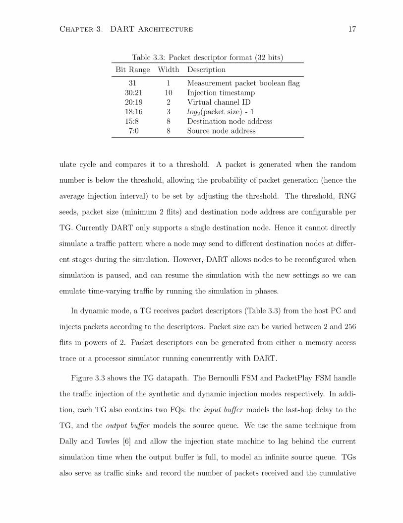
Table 3.3: Packet descriptor format (32 bits)
Bit Range Width Description
31 1 Measurement packet boolean flag30:21 10 Injection timestamp20:19 2 Virtual channel ID18:16 3 log2(packet size) - 115:8 8 Destination node address7:0 8 Source node address
ulate cycle and compares it to a threshold. A packet is generated when the random
number is below the threshold, allowing the probability of packet generation (hence the
average injection interval) to be set by adjusting the threshold. The threshold, RNG
seeds, packet size (minimum 2 flits) and destination node address are configurable per
TG. Currently DART only supports a single destination node. Hence it cannot directly
simulate a traffic pattern where a node may send to different destination nodes at differ-
ent stages during the simulation. However, DART allows nodes to be reconfigured when
simulation is paused, and can resume the simulation with the new settings so we can
emulate time-varying traffic by running the simulation in phases.
In dynamic mode, a TG receives packet descriptors (Table 3.3) from the host PC and
injects packets according to the descriptors. Packet size can be varied between 2 and 256
flits in powers of 2. Packet descriptors can be generated from either a memory access
trace or a processor simulator running concurrently with DART.
Figure 3.3 shows the TG datapath. The Bernoulli FSM and PacketPlay FSM handle
the traffic injection of the synthetic and dynamic injection modes respectively. In addi-
tion, each TG also contains two FQs: the input buffer models the last-hop delay to the
TG, and the output buffer models the source queue. We use the same technique from
Dally and Towles [6] and allow the injection state machine to lag behind the current
simulation time when the output buffer is full, to model an infinite source queue. TGs
also serve as traffic sinks and record the number of packets received and the cumulative

Chapter 3. DART Architecture 18
Figure 3.3: Traffic Generator datapath
Figure 3.4: DART Router datapath
packet latency. More statistics counters can be easily added.
3.3 Router
The Router component encapsulates the routing and allocation logic of the classic credit-
based wormhole VC router described in Section 2.1. Figure 3.4 shows the Router dat-
apath. The number of ports is set to five in our current implementation, but can be
changed by setting a Verilog parameter. We use table-based routing. Hence any de-
terministic routing algorithms can be implemented. The table contents are configurable
without reprogramming the FPGA. The configuration of the routing table also facilitates
the simulation of a wide range of topologies.

Chapter 3. DART Architecture 19
Table 3.4: Allocator and crossbar implementation cost in terms of the basic buildingblocks required in the classic router and in the DART Router (pi is the number of inputports. po is the number of output ports. v is the number of VCs per port.)
Structure Classic Router DART Router
VC Allocator piv v-to-1 arbiters and 1 v-to-1 arbiter andpov piv-to-1 arbiters 1 v-bit po-to-1 MUX
Switch Allocator pi v-to-1 arbiters and 1 piv-to-1 arbiterpo pi-to-1 arbiters
Crossbar Switch pov piv-to-1 MUXes 1 piv-to-1 MUX
(a) (b)
Figure 3.5: VC allocator implementation: (a) classic router, (b) DART Router
A 4-bit counter for each output VC is used to implement credit-based flow control.
Initial credit values represent the number of entries in the input buffer at the downstream
router. The counter is decremented when a flit is routed, and incremented when a credit
is received. The values are configurable for each VC and Router.
3.3.1 Area-Speed Trade-off
The allocators and the crossbar in the classic router are complex structures [18]. A
direct implementation is too area-consuming. Instead, the DART Router employs simple
arbiters and a multiplexer to implement the same functionality by trading off simulation

Chapter 3. DART Architecture 20
speed. Table 3.4 outlines the implementation costs of the allocators and crossbar in
the classic router and their equivalents in the DART Router. A two-stage VC allocator
(Figure 3.5a), which consists of piv v-to-1 arbiters in the first stage and pov piv-to-1
arbiters in the second stage is required because we allow flits to allocate any free VC
once the output port is determined by the routing function. Figure 3.5b shows the
DART Router VC allocator for comparison. DART’s equivalent to the classic router’s
allocators and crossbar are much smaller.
As a result of this model simplification, the Router component can only route one flit
per DART cycle. To model a 5-ported classic router, the input VCs are routed one at
a time while the global time counter is stalled so all input ports appear to be routed in
the same simulated cycle. A round-robin scheme selects an input VC to route in each
DART cycle. If a flit cannot be routed due to failed VC allocation or lack of credits
for the requested output VC, it remains in the FQ. It is considered again in the next
simulated cycle. For every simulated cycle that a flit is unable to route, its timestamp is
incremented to reflect the contention delay. When a flit is finally routed, its timestamp is
incremented by a fixed pipeline latency. This pipeline latency is configurable per Router.
3.3.2 Send-Ahead Optimization
Once a flit is routed, it waits in the Router output queue. It is forwarded to the next-hop
FQ at its scheduled dequeue time. The Router stalls when the output queue is full. If
the queue is not large enough to cover the pipeline latency, deadlock may arise when
global time is stalled because there are unprocessed input ports, but the output queue
is not drained as the head flit waits for its dequeue time. To keep the output queue size
small while avoiding deadlock, we let flits in the output queue proceed immediately to the
global interconnect so the output queue can make forward progress even when global time
stalls. The flits still arrive at the receiving FQ in order because they leave the Router in
chronological order, despite being sent ahead. Sending ahead also avoids bursty requests
Chapter 3. DART Architecture 21
to the global interconnect in the beginning of every simulated cycle. Overall interconnect
utilization is improved.
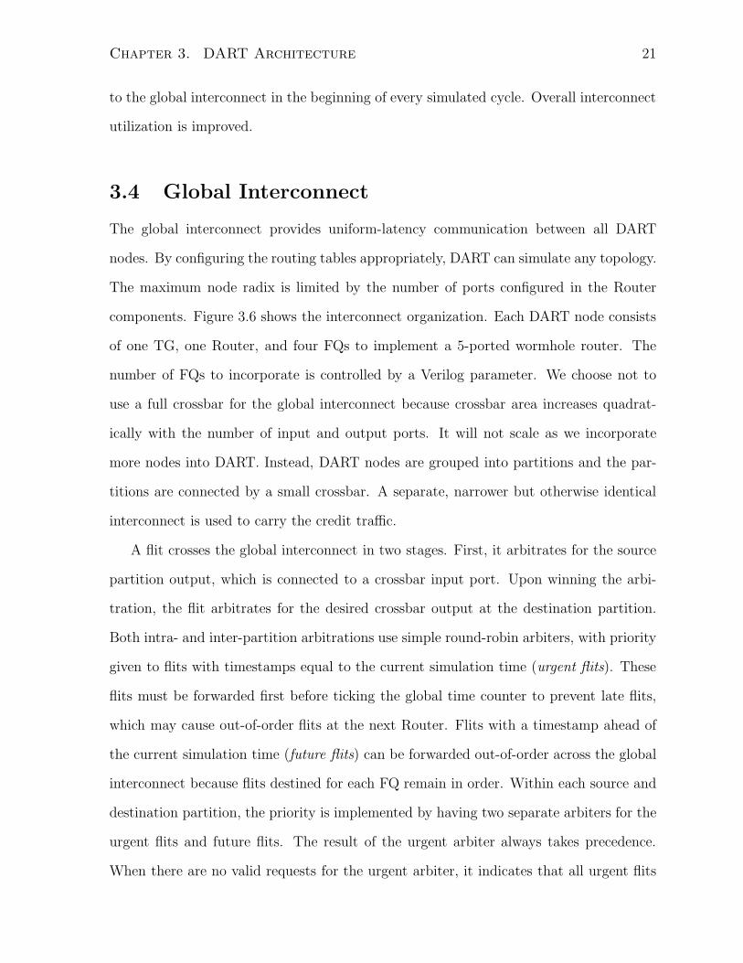
3.4 Global Interconnect
The global interconnect provides uniform-latency communication between all DART
nodes. By configuring the routing tables appropriately, DART can simulate any topology.
The maximum node radix is limited by the number of ports configured in the Router
components. Figure 3.6 shows the interconnect organization. Each DART node consists
of one TG, one Router, and four FQs to implement a 5-ported wormhole router. The
number of FQs to incorporate is controlled by a Verilog parameter. We choose not to
use a full crossbar for the global interconnect because crossbar area increases quadrat-
ically with the number of input and output ports. It will not scale as we incorporate
more nodes into DART. Instead, DART nodes are grouped into partitions and the par-
titions are connected by a small crossbar. A separate, narrower but otherwise identical
interconnect is used to carry the credit traffic.
A flit crosses the global interconnect in two stages. First, it arbitrates for the source
partition output, which is connected to a crossbar input port. Upon winning the arbi-
tration, the flit arbitrates for the desired crossbar output at the destination partition.
Both intra- and inter-partition arbitrations use simple round-robin arbiters, with priority
given to flits with timestamps equal to the current simulation time (urgent flits). These
flits must be forwarded first before ticking the global time counter to prevent late flits,
which may cause out-of-order flits at the next Router. Flits with a timestamp ahead of
the current simulation time (future flits) can be forwarded out-of-order across the global
interconnect because flits destined for each FQ remain in order. Within each source and
destination partition, the priority is implemented by having two separate arbiters for the
urgent flits and future flits. The result of the urgent arbiter always takes precedence.
When there are no valid requests for the urgent arbiter, it indicates that all urgent flits

Chapter 3. DART Architecture 22
Figure 3.6: DART’s global interconnect. Nodes are grouped into partitions so the sizeof the crossbar needed is small. The source partitions are shown at the top and thedestination partitions are shown at the bottom.
have crossed the interconnect. The global time counter is then incremented. Because it
takes a cycle to detect this condition, each simulated cycle takes at least 2 DART cycles.
The global interconnect is on the timing critical path. Hence, it is pipelined to improve
maximum achievable system clock frequency (fmax) during implementation. The pipeline
registers are inserted after the source partitions.
Because only one flit can be sent and received by a partition per DART cycle, the
partitions are a performance bottleneck. For a fixed number of DART nodes, varying the
size of the partition trades off the global interconnect throughput for implementation area.
We discuss this in more detail in Section 5.5. For our current 9-node implementation, we
use an 8 × 8 crossbar to connect the partitions. In general, the largest crossbar that fits
in the device once the nodes are implemented should be chosen.
Chapter 3. DART Architecture 23
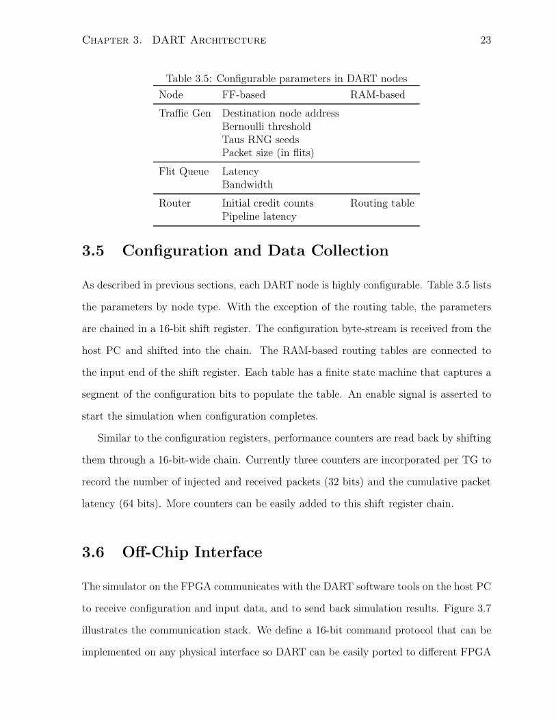
Table 3.5: Configurable parameters in DART nodes
Node FF-based RAM-based
Traffic Gen Destination node addressBernoulli thresholdTaus RNG seedsPacket size (in flits)
Flit Queue LatencyBandwidth
Router Initial credit counts Routing tablePipeline latency
3.5 Configuration and Data Collection
As described in previous sections, each DART node is highly configurable. Table 3.5 lists
the parameters by node type. With the exception of the routing table, the parameters
are chained in a 16-bit shift register. The configuration byte-stream is received from the
host PC and shifted into the chain. The RAM-based routing tables are connected to
the input end of the shift register. Each table has a finite state machine that captures a
segment of the configuration bits to populate the table. An enable signal is asserted to
start the simulation when configuration completes.
Similar to the configuration registers, performance counters are read back by shifting
them through a 16-bit-wide chain. Currently three counters are incorporated per TG to
record the number of injected and received packets (32 bits) and the cumulative packet
latency (64 bits). More counters can be easily added to this shift register chain.
3.6 Off-Chip Interface
The simulator on the FPGA communicates with the DART software tools on the host PC
to receive configuration and input data, and to send back simulation results. Figure 3.7
illustrates the communication stack. We define a 16-bit command protocol that can be
implemented on any physical interface so DART can be easily ported to different FPGA

Chapter 3. DART Architecture 24
Figure 3.7: Off-chip interface
systems. Table 3.6 shows the format of the command protocol and Table 3.7 explains
the fields. Each 16-bit word contains a 4-bit opcode and a 12-bit immediate value. It can
also be optionally followed by multiple 16-bit data words. The Control FSM interprets
the commands and generates control signals that drive the simulator core. The off-chip
interface is currently implemented over the RS232 serial port.
Table 3.6: Off-chip interface command format[15:12] 11:4 3 2 1 Bit 00 × 0 sim reset0 × 1 NA timer enable no inject measure enable0 × 2 timer value (lower 12 bits)0 × 3 timer value (higher 12 bits)0 × 4 config enable0 × 5 data request0 × 6 states request0 × 7 num packets
0 × 8 .. 0 × F Unused
3.7 Software Tools
The DART software tools run on a host PC connected to the FPGA where the hardware
simulator resides. They allow the dynamic reprogramming of the hardware simulator
after it is implemented on the FPGA. Fig. 3.8 shows the software flow. The components
are described in this section.

Chapter 3. DART Architecture 25
Table 3.7: Off-chip interface command description
Field Description
sim reset A write to this address resets the DART simulatorsim enable When set to 1, it enables the DART simulatormeasure When set to 1, all new flits generated are tagged to be measure-
ment flitsstop injection When set to 1, no more new packets will be generatedtimer enable When set to 1, the DART simulator automatically stops itself
and sends back the simulator states after timer value simulationsteps
config enable A write to this address must be followed by (N+1) 16-bit words,where the first word is equal to N and the rest contains theconfiguration bytes
data request A write to this address must be followed by a 16-bit word N
and it causes the Control Unit to send back N words throughthe TX Unit.
states request A write to this address causes the Control Unit to send backfour 16-bit words indicating the current state of the simulator(debugging only)
num packets A write to this address must be followed by 2×N 16-bit wordsthat contain N 32-bit packet descriptors. The value of N isencoded in the lower 12 bits of this command.
3.7.1 Configuration Generation
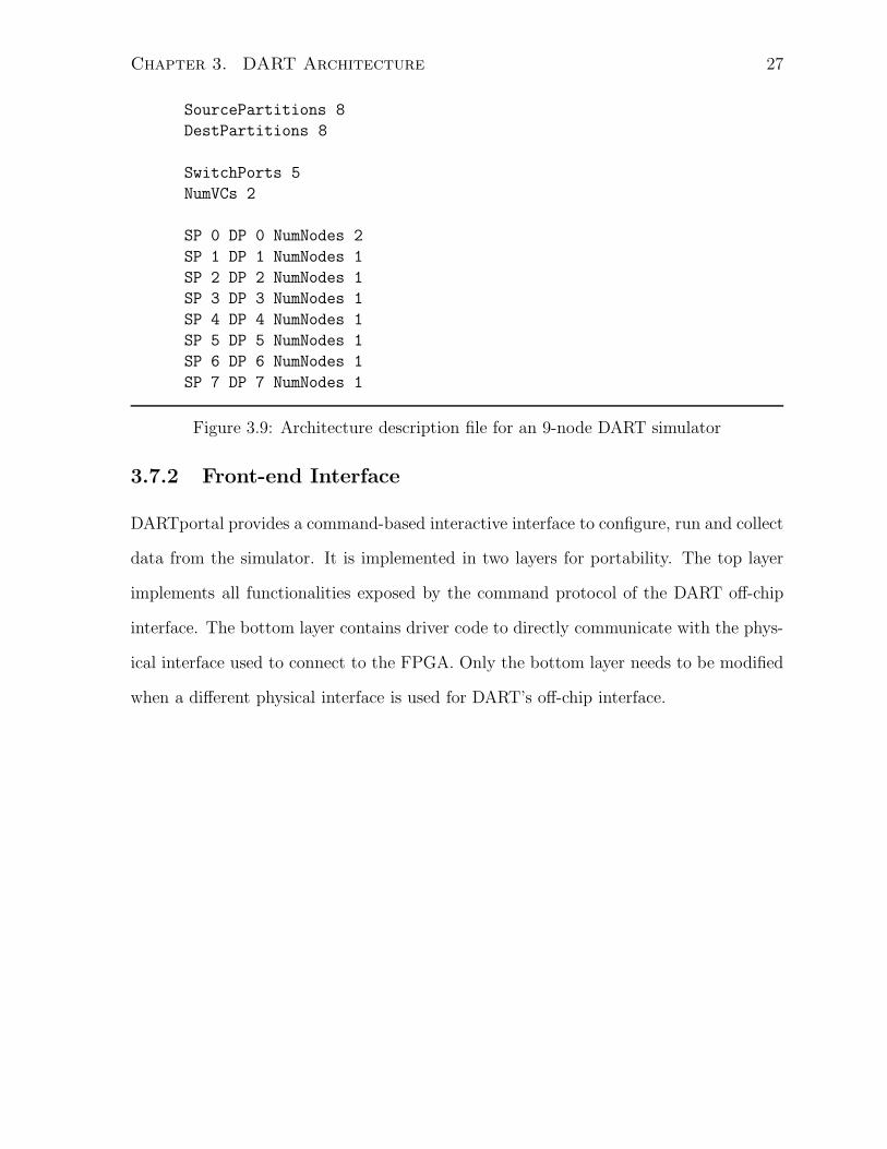
DARTgen creates the configuration byte-stream from an Architecture Description File
(ADF) and a Network Description File (NDF). Excerpts of the ADF and NDF are shown
in Figures 3.9 and 3.10. The ADF specifies the on-chip architecture by listing the number
of partitions on the interconnect and the number of nodes within each partition. Each
partition is identified by its source partition ID (SP) and destination partition ID (DP).
The NDF describes the user network to simulate, including the topology, routing tables,
traffic pattern, and properties of individual links and routers.
The DARTgen flow consists of three stages: network extraction, placement, and
byte-stream generation. In network extraction, DARTgen constructs a graph of the
user network from the NDF. Each vertex represent a router and its host node. The edges
represent the links between routers. The vertices and edges are annotated with properties

Chapter 3. DART Architecture 26
Figure 3.8: DART software flow. DARTgen creates the configuration byte-stream fromuser specifications. DARTportal provides an interactive interface for the user to controlthe hardware simulator.
specified in the NDF. A model of the on-chip partition hierarchy is also constructed from
the ADF.
In placement, vertices and edges are mapped to Routers and Flit Queues, with the
host node in each vertex mapped to the Traffic Generator connected to the correspond-
ing Router. We use a round-robin scheme to balance the number of used nodes across
different partitions. This provides sufficient load balancing because the on-chip com-
munication bottleneck is within each partition, where the nodes contend for the shared
access to the inter-partition crossbar. Intra-partition contention can be further reduced
by grouping neighbors of a common node in the user network into one partition. Because
the common node can only send to one member of the group in a simulated cycle, there
is less competition within the group to use the crossbar output.
Finally in byte-stream generation, the configuration bytes for the architecture nodes
are printed to a file in the order that they are connected in the configuration chain
on-chip. This file is used by the front-end tool DARTportal to program the on-chip
simulator.
Chapter 3. DART Architecture 27
SourcePartitions 8
DestPartitions 8
SwitchPorts 5
NumVCs 2
SP 0 DP 0 NumNodes 2
SP 1 DP 1 NumNodes 1
SP 2 DP 2 NumNodes 1
SP 3 DP 3 NumNodes 1
SP 4 DP 4 NumNodes 1
SP 5 DP 5 NumNodes 1
SP 6 DP 6 NumNodes 1
SP 7 DP 7 NumNodes 1
Figure 3.9: Architecture description file for an 9-node DART simulator
3.7.2 Front-end Interface
DARTportal provides a command-based interactive interface to configure, run and collect
data from the simulator. It is implemented in two layers for portability. The top layer
implements all functionalities exposed by the command protocol of the DART off-chip
interface. The bottom layer contains driver code to directly communicate with the phys-
ical interface used to connect to the FPGA. Only the bottom layer needs to be modified
when a different physical interface is used for DART’s off-chip interface.

Chapter 3. DART Architecture 28
NumNodes 9
NumSwitches 9
ChannelLatency 1
ChannelBandwidth 1
NumVCPerChannel 2
SwitchPorts 5
InitialCredits 5
RouterPipeLatency 5
NumWarmupSteps 30
# Traffic pattern (type, source node -> dest node, size, interval)
Traffic CBR Node 0 -> Node 7 2 4
Traffic CBR Node 1 -> Node 3 2 4
...
# Topology (Host Node -> Switch addr:port, latency, bandwidth)
Top Node 0 -> Switch 0:0 1 1
Top Node 1 -> Switch 1:0 1 1
...
# 9-node MESH (router1:port -> router2:port, latency, bandwidth)
Top Switch 0:3 -> Switch 1:1 1 1
Top Switch 0:4 -> Switch 3:2 1 1
Top Switch 1:3 -> Switch 2:1 1 1
...
# Deadlock-free routing tables
# Switch 0 -> * (-> dest_addr {output_port:VC})
Route Switch 0 -> 0 { 0:0 }
Route Switch 0 -> 1 { 3:0 }
...
Figure 3.10: Excerpt of the network description file for a 9-node mesh

Chapter 4
Implementation
We design the DART components in Verilog HDL. Device specific constructs are avoided
whenever possible so the simulator core can be implemented on different FPGA sys-
tems with minimal changes. Prior to developing the HDL, we develop a cycle-accurate
architecture simulator in C++ to explore different design options. This simulator also
serves as the design specification, which is used to verify the HDL design. To demon-
strate the functionality of DART and to obtain real measurement of simulation speed, we
implement a 9-node DART on a Xilinx University Program Virtex-II Pro Development
System (XUPV2P) [27]. We also discuss the strategies to scale up DART to target a
Virtex 5 FPGA. However, we do not have the hardware to test actual performance of
the Virtex 5 implementation. We use the Xilinx ISE 10.1 software suite for synthesis and
implementation.
4.1 9-node DART on XUPV2P
The XUPV2P platform contains a Virtex-II Pro 2VP30 FPGA that has 27,392 logic cells
and 136 embedded RAM blocks. A logic cell consists of a 4-input lookup table (LUT)
and a flip-flop (FF). Each block-RAM contains 18 Kb and has two read/write ports.
The maximum width of a port is 36 bits. Table 4.1 shows the resource breakdown of
29

Chapter 4. Implementation 30
Table 4.1: Resource utilization breakdown of a 9-node DART on a XC2VP30 FPGA
ModulePer-Module Resource Utilization % of Total
4-LUTs FFs Block RAMs 4-LUTs
Traffic Generator 691 500 2 24.7%Flit Queue 305 145 1 43.5%
Router 612 201 0.5 21.8%Global Interconnect 2144 104 0 8.5%
Control Unit 152 70 0 0.6%UART interface 208 171 1 0.8%
Total 26,38 13,192 99 100%% of Available 96% 48% 72%
Table 4.2: FIFO Usage in 9-node DART
Usage Width (bits) Depth Total Number
Per-VC Flit buffer in FQ 36 64 108Credit buffer in FQ 12 64 54
Router output flit buffer 36 16 9Router output credit buffer 12 16 9
the DART components as implemented on the XUPV2P platform. Because every two
Routers share a dual-ported routing table, which is implemented using a dual-port block-
RAM, each Router uses 0.5 block-RAMs on average. The maximum number of DART
nodes that fit on this FPGA is 9. Each node consists of one TG, one Router with 5
ports, and four FQs with 2 VCs each. We use 8 partitions in the global interconnect,
which is the largest that fits inside the area constraint. The final implementation runs
at 50 MHz.
4.1.1 RAM Optimization
DART uses FIFO buffers extensively. Table 4.2 enumerates the usage. FIFOs can be
implemented either in block-RAMs or LUT-based shift registers on an FPGA. When
implemented in a RAM, a FIFO takes up both ports on the RAM block to allow simulta-
neous read and write operations. The 2VP30 FPGA does not have enough RAM blocks

Chapter 4. Implementation 31
to accommodate all FIFOs in the 9-node DART. Our solution is two-fold: First, because
a FQ can receive at most one flit and send one flit per DART cycle, the VC buffers in the
FQ can share a single statically partitioned RAM block for storage. The FIFO output
registers and control logic must be replicated. Second, we implement the shallow output
buffers in the Routers using LUT-based SRL16 shift registers [26].
Because routing tables are read-only during simulation, we can pack two into each
dual-port block-RAM to utilize both ports. One of the ports is configured to be read-
/write and is used to configure the table contents.
4.1.2 Serial Interface
We implement the DART off-chip interface over the RS232 serial port because it is more
lightweight than other options. A UART module on the FPGA handles serial communi-
cation with the host PC. The UART can operate at up to 115200 bps. This is sufficient
for configuration and stats collection because they are only performed once before and
after the simulation. However, it is too slow for packet injection as it only allows an
average of 356 packet descriptors to be injected to each of the 9 nodes per second. As-
suming 5% simulated packet injection, using the UART interface limits simulation speed
to 7 KHz. Faster interface options will be investigated in future work.
4.2 Scaling DART to Virtex 5
We investigate scaling up DART to target the Virtex 5 LX330T FPGA. In comparison to
the 2VP30 device, the LX330T provides 10× more LUTs and FFs but only 4× more 18
Kb block-RAMs. Because of the limited number of block-RAMs, an unmodified DART
can only scale up to 32 nodes on the LX330T device, with only 40% logic utilization. To
balance the RAM and logic utilization, we can extend the block-RAM sharing scheme
currently used between flit buffers within a FQ to FQs in the same partition. Because

Chapter 4. Implementation 32
each partition receives one flit per DART cycle, the sharing does not change DART’s
behavior. Using this scheme, each 18 Kb block-RAM can accommodate 4 FQs with 2
VCs each if the FIFO dimensions in Table 4.2 are used. This will allow DART to scale
to 64 nodes, limited by the amount of logic resources on the FPGA.
A limitation of the current DART design is that the computation logic of each DART
node cannot be easily time-shared between multiple contexts to allow simulation of NoCs
larger than what can currently fit in an FPGA. This is because a significant portion of
each DART node is devoted to state registers (implemented using logic cell flip flops)
and control state machines. They must be replicated for each context that shares the
pipeline, thus limiting the potential area saving. Multiple contexts can be supported by
storing the state registers in a block-RAM. This requires the DART components to be
further pipelined to accommodate the additional state look-up latency.
Chapter 5
Analysis
In this section we validate DART’s simulation results using Booksim as a reference. We
also compare the speedup achieved using our Virtex-II Pro implementation. Finally we
investigate the performance cost of a programmable simulator architecture and DART’s
scalability.
5.1 Methodology
We use both the architecture simulator of DART and the XUPV2P implementation of
DART to collect results for this section. Results shown in Sections 5.2, 5.4, 5.5 and
5.6 are obtained using the architecture simulator because we explore different DART
architectures and the architectural simulator allows more statistics to be collected for
analysis. The timing results shown in Section 5.3 are measured on the FPGA board. Since
the architectural simulator is also the design specification for the Verilog implementation
of DART, their results agree when the same configuration is used.
5.2 Correctness
To verify DART’s correctness, we simulate a 9-node mesh network and compare the
measured average latency reported by Booksim and DART (Fig. 5.1). We obtain two
33
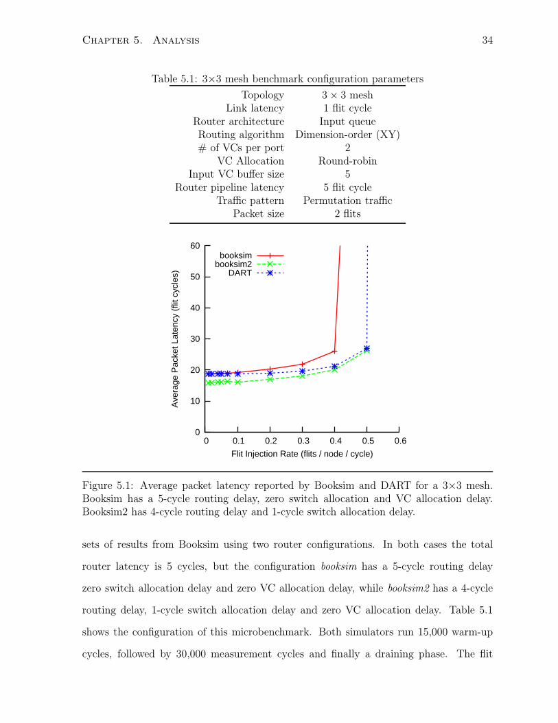
Chapter 5. Analysis 34
Table 5.1: 3×3 mesh benchmark configuration parameters
Topology 3 × 3 meshLink latency 1 flit cycle
Router architecture Input queueRouting algorithm Dimension-order (XY)# of VCs per port 2
VC Allocation Round-robinInput VC buffer size 5
Router pipeline latency 5 flit cycleTraffic pattern Permutation traffic
Packet size 2 flits
0
10
20
30
40
50
60
0 0.1 0.2 0.3 0.4 0.5 0.6
Ave
rage
Pac
ket L
aten
cy (
flit c
ycle
s)
Flit Injection Rate (flits / node / cycle)
booksimbooksim2
DART
Figure 5.1: Average packet latency reported by Booksim and DART for a 3×3 mesh.Booksim has a 5-cycle routing delay, zero switch allocation and VC allocation delay.Booksim2 has 4-cycle routing delay and 1-cycle switch allocation delay.
sets of results from Booksim using two router configurations. In both cases the total
router latency is 5 cycles, but the configuration booksim has a 5-cycle routing delay
zero switch allocation delay and zero VC allocation delay, while booksim2 has a 4-cycle
routing delay, 1-cycle switch allocation delay and zero VC allocation delay. Table 5.1
shows the configuration of this microbenchmark. Both simulators run 15,000 warm-up
cycles, followed by 30,000 measurement cycles and finally a draining phase. The flit

Chapter 5. Analysis 35
0
500
1000
1500
2000
2500
3000
3500
4000
4500
<7 8 9 10 11 12 13 14 15 16 17 18 19 20 21 22 23 24 25 26 27 28 29 30 31 32 33 34 35 36 37 38 39 40 41 42 43 44 45 46 47 48 49>=50
Fre
quen
cy (
# of
pac
kets
)
Average Packet Latency (flit cycles)
booksim1DART
Figure 5.2: 3 × 3 Mesh. Packet latency distribution measured by Booksim (booksim1)and DART at flit injection rate = 0.4
injection rate is varied from 0.01 until saturation. DART tracks Booksim closely at
low injection rates. At higher injection rates, the one-stage pipeline used in the Router
results in a less accurate latency measurement. This is evident in that DART latency is
enveloped by the two Booksim configurations, which have the same overall router latency
but different latencies at each stage. To further investigate the mismatch, Fig. 5.2 shows
the distribution of packet latencies at 0.4 flits per cycle. The peaks at 8, 14, 20, 26, and
32 correspond to the zero-load latencies for 0, 1, 2, 3, and 4-hop paths. The lower peaks
reflect the queuing delay and resource contention the packets experience at the routers.
Booksim has a much longer tail than DART. Because all contentions (buffer, VC, and
switch) are modeled in one stage in the DART Router, DART may underpredict the
latency for a flit to acquire all resources. However, the similar overall shapes of the two
distribution increases our confidence that DART produces useful predictions of network
performance.
5.3 Speedup vs. Software Simulation
In Fig. 5.3 we evaluate the 3×3 mesh benchmark described in Table 5.1 on the XUPV2P
DART implementation and compare the simulation speed to Booksim. For the Booksim
baseline, we measure the execution time of the main loop, excluding network setup, on a
2.66 GHz Core 2 Quad Linux workstation. Each data point is an average over 20 runs. We

Chapter 5. Analysis 36
0
10000
20000
30000
40000
50000
60000
70000
0 0.1 0.2 0.3 0.4 0.5 0.6
Boo
ksim
Spe
ed (
cycl
es /
s)
Flit Injection Rate (flits / node / cycle)
(a)
0
50
100
150
200
0 0.1 0.2 0.3 0.4 0.5 0.6
DA
RT
Spe
ed /
Boo
ksim
Spe
ed
Flit Injection Rate (flits / node / cycle)
(b)
Figure 5.3: DART performance: (a) Booksim simulation speed, (b) Speedup achieved byDART vs. Booksim
measure DART’s execution time in DARTportal from the sending of the “Run” command
and until the end-of-simulation signal is received back from the simulator. Configuration
time is excluded. The speedup is the ratio of the number of cycles simulated per second
in DART to that in Booksim. We observe that Booksim’s simulation speed decreases
with increasing injection rate. DART’s speed is roughly constant, with all measured
runtimes falling within 3% (0.528 ms) of the average (20.5 ms for 50,000 cycles)—this
is because DART’s execution time increases slowly with traffic, and is largely masked
by the high IO overhead to send and read-back commands to/from the simulator, which
accounts for over 50% of the measured time (about 11.7 ms). As a result, DART achieves
greater speedup at higher packet injection rates. The IO overhead can also be amortized
in longer-running simulations of networks larger than the 3×3 mesh used here.
5.4 Cost of Programmability
The main alternative to DART’s programmable architecture is one that is directly laid-
out in the FPGA fabric. In this section we measure the performance cost of DART’s
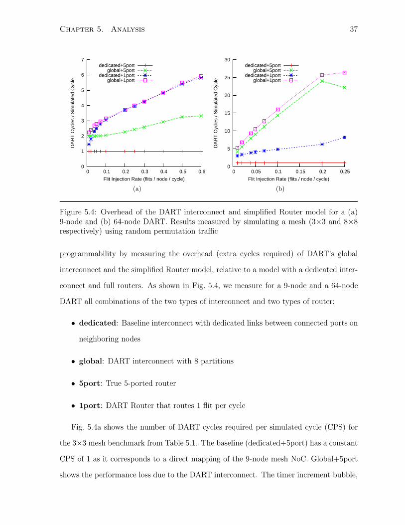
Chapter 5. Analysis 37
0
1
2
3
4
5
6
7
0 0.1 0.2 0.3 0.4 0.5 0.6
DA
RT
Cyc
les
/ Sim
ulat
ed C
ycle
Flit Injection Rate (flits / node / cycle)
dedicated+5portglobal+5port
dedicated+1portglobal+1port
(a)
0
5
10
15
20
25
30
0 0.05 0.1 0.15 0.2 0.25
DA
RT
Cyc
les
/ Sim
ulat
ed C
ycle
Flit Injection Rate (flits / node / cycle)
dedicated+5portglobal+5port
dedicated+1portglobal+1port
(b)
Figure 5.4: Overhead of the DART interconnect and simplified Router model for a (a)9-node and (b) 64-node DART. Results measured by simulating a mesh (3×3 and 8×8respectively) using random permutation traffic
programmability by measuring the overhead (extra cycles required) of DART’s global
interconnect and the simplified Router model, relative to a model with a dedicated inter-
connect and full routers. As shown in Fig. 5.4, we measure for a 9-node and a 64-node
DART all combinations of the two types of interconnect and two types of router:
• dedicated: Baseline interconnect with dedicated links between connected ports on
neighboring nodes
• global: DART interconnect with 8 partitions
• 5port: True 5-ported router
• 1port: DART Router that routes 1 flit per cycle
Fig. 5.4a shows the number of DART cycles required per simulated cycle (CPS) for
the 3×3 mesh benchmark from Table 5.1. The baseline (dedicated+5port) has a constant
CPS of 1 as it corresponds to a direct mapping of the 9-node mesh NoC. Global+5port
shows the performance loss due to the DART interconnect. The timer increment bubble,

Chapter 5. Analysis 38
described in Section 3.4 on page 21, limits the minimum CPS to 2. Increased traffic
causes more contention over the interconnect and lower CPS. Dedicated+1port shows
the performance loss due to the serial processing of input VCs in the Router. CPS
increases with network traffic, as each Router has more input VCs in use. Global+1port
shows that for 9 nodes, because of the small number of nodes and low throughput of the
Router, the global interconnect is not the performance bottleneck. However, Fig. 5.4b
shows that more nodes in a large DART increases contention for the global interconnect
and it can become the bottleneck. As traffic load increases, it takes more DART cycles
for all flits of a given simulated cycle to cross the global interconnect. Consequently,
CPS increases linearly with traffic. The simulated network saturates when the per node
injection rate is 0.25 flits/simulated cycle. Because the overall traffic in the network does
not increase beyond this point, CPS levels off and we see the knee inflection in the figure.
To avoid limiting simulation performance, an appropriate interconnect size should be
chosen for each DART implementation.
Compared to the baseline, DART’s interconnect uses more area than dedicated links,
but the overhead is compensated by the simplified Router. Thus, the overall area cost
is comparable to published results from existing direct mapped emulators [8, 21]. We
believe the performance penalty is a worthwhile trade-off for the ability to reprogram the
simulator without hardware modification.
5.5 Scalability
We explore the scalability of DART beyond 9 nodes when a larger FPGA becomes avail-
able using the architecture simulator. The predicted runtime does not include commu-
nication overhead to and from the host PC. It provides an upper bound to the actual
attainable speedup.

Chapter 5. Analysis 39
0
10
20
30
40
50
60
70
0 5 10 15 20 25 30 35 40 45
Boo
ksim
Spe
ed (
1000
cyc
les
/ s)
Aggregated Transfers (flit hops / cycle)
3x3 mesh4x4 mesh6x6 mesh8x8 mesh
(a)
5000
10000
15000
20000
25000
0 5 10 15 20 25 30 35 40 45
DA
RT
Spe
ed (
1000
cyc
les
/ s)
Aggregated Transfers (flit hops / cycle)
3x3 mesh4x4 mesh6x6 mesh8x8 mesh
(b)
Figure 5.5: Booksim (a) and DART (b) simulation speed for different network sizes
5.5.1 Performance Scaling
Fig. 5.5 highlights the different scaling trends of Booksim and DART for four mesh
networks of different sizes. The aggregated flit transfers per simulated cycle is the product
of the flit rate, average number of hops between packet source and destination pairs and
number of nodes. It measures the overall amount of in-flight traffic that traverses the
network every cycle. For a given simulation, Booksim’s speed depends on both the size
of the simulated network and also on the amount of network activity. Because Booksim
is cycle-based, it must simulate every cycle including those when the simulated network
is idle. This overhead dominates simulation time for large networks and the network
activity level becomes an insignificant factor for performance. DART’s simulated time
advances faster when the simulated network is idle. Its simulation speed thus depends
only on the amount of network activity. As a result, DART’s speedup over Booksim
varies from 300× for the 3×3 mesh to 2000× for the 8×8 mesh. The design focus for
DART is on improving area efficiency so more simulator nodes can be implemented on a
given FPGA.

Chapter 5. Analysis 40
0
2000
4000
6000
8000
10000
12000
14000
16000
18000
9 16 25 36 64
DA
RT
Spe
ed (
1000
cyc
les
/ s)
Torus Size (number of nodes)
SP4_DP4SP8_DP4SP8_DP8
SP16_DP8SP16_DP16
(a)
0
2000
4000
6000
8000
10000
12000
14000
16000
18000
9 16 25 36 64
DA
RT
Spe
ed (
1000
cyc
les
/ s)
Torus Size (number of nodes)
SP4_DP4SP8_DP4SP8_DP8
SP16_DP8SP16_DP16
(b)
Figure 5.6: Performance impact of global interconnect sizes, evaluated using torus net-works (a) flit injection rate = 0.1 (b) flit injection rate = 0.5
5.5.2 Performance vs. Resource Utilization
The global interconnect is the main performance bottleneck in the DART architecture
because nodes within the same partition compete for access to the input and output ports
on the inter-partition crossbar. Fig. 5.6 shows the performance impact of various crossbar
configurations for different DART sizes, where SPx DPy denotes a global interconnect
with an x × y crossbar. Each data point is evaluated by simulating a torus network
using the DART global interconnect. We use permutation traffic for each simulated
network. The results for the SP4 DP8 and SP8 DP16 configurations are not shown here
because their performance is similar to that of the SP8 DP4 and SP16 DP8 configurations
respectively. Relative to a square crossbar, doubling the number of either the input ports
or output ports only improves performance slightly as the asymmetric configurations do
not fully remove the contention within partitions.
Fig. 5.7 shows the total resource utilization of the global interconnect for a 64-node
DART. The source partitions encapsulate the arbitration logic to allow sharing of the
inter-partition crossbar inputs; the area of each source partition grows roughly linearly

Chapter 5. Analysis 41
0
1000
2000
3000
4000
5000
6000
7000
8000
9000
10000
4x4 4x8 8x4 8x8 8x16 16x816x16
Logi
c U
tiliz
atio
n (4
-LU
Ts)
Interconnect Crossbar Size (SPxDP)
SourcePartitionsDestPartitions
Figure 5.7: Resource utilization of different interconnect sizes
with the number of nodes in the partition. As a result, for a fixed number of DART nodes,
the aggregated resources used by the source partitions are roughly constant, irrespective
of the number of source partitions. The destination partition contains the multiplexers
that implement the crossbar and the broadcast logic that enable the sharing of the inter-
partition crossbar outputs, and it grows linearly to the number of source partitions. For
the range of interconnect sizes considered here, because the source partitions start off as
a significant portion of the total area, the overall LUT usage of the interconnect grows
roughly linearly with the number of ports. For best performance, the largest square
crossbar that meets the area constraint should always be used.
5.6 Case Studies
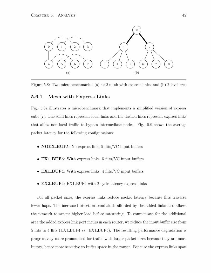
We choose two examples (Fig. 5.8) to demonstrate DART’s ability to simulate irregular
network configurations. The results presented in this section are simulated using a ran-
domly generated permutation traffic pattern. Each configuration requires generating a
new byte-stream file, but the DART simulator is only synthesized once on the FPGA.
Chapter 5. Analysis 42
0 1
4
2
5
3
6 7
(a)
0
1 2
3 4 5 6 7 8
(b)
Figure 5.8: Two microbenchmarks: (a) 4×2 mesh with express links, and (b) 2-level tree
5.6.1 Mesh with Express Links
Fig. 5.8a illustrates a microbenchmark that implements a simplified version of express
cube [7]. The solid lines represent local links and the dashed lines represent express links
that allow non-local traffic to bypass intermediate nodes. Fig. 5.9 shows the average
packet latency for the following configurations:
• NOEX BUF5: No express link, 5 flits/VC input buffers
• EX1 BUF5: With express links, 5 flits/VC input buffers
• EX1 BUF4: With express links, 4 flits/VC input buffers
• EX2 BUF4: EX1 BUF4 with 2-cycle latency express links
For all packet sizes, the express links reduce packet latency because flits traverse
fewer hops. The increased bisection bandwidth afforded by the added links also allows
the network to accept higher load before saturating. To compensate for the additional
area the added express link port incurs in each router, we reduce the input buffer size from
5 flits to 4 flits (EX1 BUF4 vs. EX1 BUF5). The resulting performance degradation is
progressively more pronounced for traffic with larger packet sizes because they are more
bursty, hence more sensitive to buffer space in the router. Because the express links span

Chapter 5. Analysis 43
two hops, we increase their latency to 2 cycles while keeping the latency of other links at
1 cycle (EX2 BUF4). This configuration causes higher latency for large packets because
credits take longer to replenish on the slower express links. However, the network still
saturates later than the NOEX BUF5 baseline.
5.6.2 Tree
Fig. 5.8b illustrates a tree where two sub-trees are linked by a root router, where the bold
lines represent global links. This organization captures the essence of building blocks in
a hierarchical on-chip network. Only the leaf nodes generate and receive traffic, and 50%
of the generated traffic cross the root router. Fig. 5.10 shows the average packet latency
for the following configurations:
• BUF5 BW1: Unit latency and bandwidth for all links, 5 flits/VC input buffers
• BUF5 BW2: BUF5 BW1, bandwidth = 2 flits/cycle on global links
• BUF10 BW1: BUF5 BW1 with 10 flits/VC input buffers
• BUF10 BW2: BUF5 BW2, with 10 flits/VC input buffers
For all packet sizes, increasing the global link bandwidth (BUF5 BW2 vs. BUF5 BW1,
BUF10 BW2 vs. BUF10 BW1) does not significantly improve packet latency because all
flits crossing the global links must be first stored in the buffers of the gateway routers
(nodes 1 and 2), which form the performance bottleneck. Increasing the buffer space
to 10 flits significantly reduces latency. Again the reduction is greater for large packets
because bursty traffic is more sensitive to buffer sizes. Moreover, Fig. 5.10c and 5.10d
show that once the buffer space bottleneck is removed, increasing global link bandwidth
can provide additional performance improvement.

Chapter 5. Analysis 44
10
15
20
25
30
35
40
0 0.1 0.2 0.3 0.4 0.5
Ave
rage
Pac
ket L
aten
cy (
flit c
ycle
s)
Flit Injection Rate (flits / node / cycle)
NOEX_BUF5EX1_BUF5EX1_BUF4EX2_BUF4
(a)
15
20
25
30
35
40
45
50
0 0.1 0.2 0.3 0.4 0.5 0.6
Ave
rage
Pac
ket L
aten
cy (
flit c
ycle
s)
Flit Injection Rate (flits / node / cycle)
NOEX_BUF5EX1_BUF5EX1_BUF4EX2_BUF4
(b)
20
30
40
50
60
70
80
0 0.1 0.2 0.3 0.4 0.5 0.6
Ave
rage
Pac
ket L
aten
cy (
flit c
ycle
s)
Flit Injection Rate (flits / node / cycle)
NOEX_BUF5EX1_BUF5EX1_BUF4EX2_BUF4
(c)
50
60
70
80
90
100
0 0.1 0.2 0.3 0.4 0.5 0.6
Ave
rage
Pac
ket L
aten
cy (
flit c
ycle
s)
Flit Injection Rate (flits / node / cycle)
NOEX_BUF5EX1_BUF5EX1_BUF4EX2_BUF4
(d)
Figure 5.9: Express links performance: (a) 2-flit packets, (b) 4-flit packets, (c) 8-flitpackets, and (d) 16-flit packets

Chapter 5. Analysis 45
27
28
29
30
31
32
33
34
0 0.05 0.1 0.15 0.2
Ave
rage
Pac
ket L
aten
cy (
flit c
ycle
s)
Flit Injection Rate (flits / node / cycle)
BUF5_BW1BUF5_BW2
BUF10_BW1BUF10_BW2
(a)
20
30
40
50
60
70
80
0 0.05 0.1 0.15 0.2 0.25 0.3
Ave
rage
Pac
ket L
aten
cy (
flit c
ycle
s)
Flit Injection Rate (flits / node / cycle)
BUF5_BW1BUF5_BW2
BUF10_BW1BUF10_BW2
(b)
30
40
50
60
70
80
90
100
0 0.05 0.1 0.15 0.2 0.25 0.3
Ave
rage
Pac
ket L
aten
cy (
flit c
ycle
s)
Flit Injection Rate (flits / node / cycle)
BUF5_BW1BUF5_BW2
BUF10_BW1BUF10_BW2
(c)
40
50
60
70
80
90
100
0 0.05 0.1 0.15 0.2 0.25 0.3
Ave
rage
Pac
ket L
aten
cy (
flit c
ycle
s)
Flit Injection Rate (flits / node / cycle)
BUF5_BW1BUF5_BW2
BUF10_BW1BUF10_BW2
(d)
Figure 5.10: Tree performance: (a) 2-flit packets, (b) 4-flit packets, (c) 8-flit packets and(d) 16-flit packets

Chapter 6
Conclusions
We have presented a software-programmable overlay architecture for NoC simulation on
FPGAs. By decoupling the simulator architecture from the architecture of the simu-
lated NoC and virtualizing simulation time, DART improves upon existing FPGA-based
emulators by eliminating the high cost of modifying and resynthesizing the hardware em-
ulator when simulating different NoCs. At the same time, DART is significantly faster
than software NoC simulators. Using an implementation of a 9-node DART simulator on
a Virtex II Pro FPGA, we demonstrate over 100-fold speedup over Booksim while main-
taining a similar level of accuracy. Through two examples, we also show that irregular
NoCs can be easily set up and simulated on DART.
6.1 Contributions
This dissertation makes the following contributions:
1. An abstraction model for NoC simulation on FPGAs and the demonstration of the
feasibility of a software configurable FPGA-based NoC simulator with negligible
area overhead relative to existing emulators that do not support configuration.
2. A comparison of the performance of the DART simulator to the well-known software
46
Chapter 6. Conclusions 47
NoC simulator Booksim and the demonstration of over 100-fold speedup.
3. An implementation of DART on a Xilinx FPGA and software configuration tools
that will be publicly released so they can be built upon in future research.
6.2 Future Work
This work opens up a few avenues of future research: First, the one-to-one mapping
between simulated nodes and DART nodes limits the maximum size of the NoC that
can be simulated on a FPGA. Time-multiplexing a simulator node between multiple
simulated threads is a technique used in FPGA-based processor simulators to enable
large-scale simulation on a single FPGA. We need to investigate how DART nodes can
be efficiently pipelined to support multithreading. Second, the simple Router cannot
easily model adaptive routing algorithms or more sophisticated router architectures such
as speculative routing. Directly replacing DART Routers with soft processors may result
in significantly slower simulation due to software overhead. Future work can explore
specializing a soft processor for routing operations. Finally, the long term goal of this
research is to build a fast and scalable full system simulator infrastructure to enable
large-scale many-core architecture research. Because the communication fabric is an
important component of any many-core architecture, we believe DART is an essential
building block to the full system simulator infrastructure.

Bibliography
[1] N. Agarwal, T. Krishna, Li-Shiuan Peh, and N.K. Jha. GARNET: A detailed on-chip
network model inside a full-system simulator. In Proc. Int’l Symp. on Performance
Analysis of Systems and Software, April 2009.
[2] T.W. Ainsworth and T.M. Pinkston. Characterizing the Cell EIB On-Chip Network.
IEEE Micro, pages 6–14, 2007.
[3] M. Baron. The Single-Chip Cloud Computer. Microprocessor Report, April 26, 2010.
[4] E.S. Chung, E. Nurvitadhi, J.C. Hoe, B. Falsafi, and K. Mai. PROToFLEX: FPGA-
accelerated Hybrid Functional Simulator. In Proc. Int’l Parallel and Distributed
Processing Symposium, March 2007.
[5] William Dally and Brian Towles. Route packets, not wires: on-chip interconnection
networks. In Proc. Design Automation Conference, 2001.
[6] William Dally and Brian Towles. Principles and Practices of Interconnection Net-
works. Morgan Kaufmann Publishers Inc., San Francisco, CA, USA, 2003.
[7] W.J. Dally. Express cubes: Improving the performance of k-ary n-cube interconnec-
tion networks. IEEE Transactions on Computers, pages 1016–1023, 1991.
[8] N. Genko, D. Atienza, G. De Micheli, J.M. Mendias, R. Hermida, and F. Catthoor.
A complete network-on-chip emulation framework. In Proc. Design, Automation
and Test in Europe, March 2005.
48

Bibliography 49
[9] Nikolaos Hardavellas, Stephen Somogyi, Thomas F. Wenisch, Roland E. Wunder-
lich, Shelley Chen, Jangwoo Kim, Babak Falsafi, James C. Hoe, and Andreas G.
Nowatzyk. SimFlex: a fast, accurate, flexible full-system simulation framework for
performance evaluation of server architecture. SIGMETRICS Perform. Eval. Rev.,
31(4):31–34, 2004.
[10] J.L. Hennessy and D.A. Patterson. Computer Architecture: A Quantitative Ap-
proach. Morgan Kaufmann, 4th edition, 2007.
[11] N.E. Jerger and L.S. Peh. On-Chip Networks. Synthesis Lectures on Computer
Architecture, 2009.
[12] Y.H. Kao, N. Alfaraj, M. Yang, and H.J. Chao. Design of High-Radix Clos Network-
on-Chip. In Fourth Proc. Int’l Symp. on Networks-on-Chip, pages 181–188. IEEE,
2010.
[13] J. Kim, J. Balfour, and W.J. Dally. Flattened Butterfly Topology for On-Chip
Networks. In 40th Proc. Int’l Symp. on Microarchitecture, pages 172–182, 2007.
[14] Y.E. Krasteva, F. Criado, E. de la Torre, and T. Riesgo. A Fast Emulation-Based
NoC Prototyping Framework. In Proc. Int’l Conf. on Reconfigurable Computing and
FPGAs, Dec. 2008.
[15] P. L’Ecuyer. Maximally equidistributed combined Tausworthe generators. Mathe-
matics of Computation, 65(213):203–214, 1996.
[16] M. Lis, K.S. Shim, M.H. Cho, P. Ren, O. Khan, and S. Devadas. DARSIM: a Parallel
Cycle-Level NoC Simulator. In 6th Annual Workshop on Modeling, Benchmarking
and Simulation, June 2010.
[17] Milo M. K. Martin, Daniel J. Sorin, Bradford M. Beckmann, Michael R. Marty,
Min Xu, Alaa R. Alameldeen, Kevin E. Moore, Mark D. Hill, and David A.

Bibliography 50
Wood. Multifacet’s general execution-driven multiprocessor simulator (GEMS)
toolset. SIGARCH Comput. Archit. News, 33(4):92–99, 2005.
[18] L.S. Peh and W.J. Dally. A delay model and speculative architecture for pipelined
routers. In Seventh Proc. Int’l Symp. on High-Performance Computer Architecture,
2001.
[19] M. Pellauer, M. Vijayaraghavan, M. Adler, Arvind, and J. Emer. A-Ports: An
Efficient Abstraction for Cycle-Accurate Performance Models on FPGAs. In Proc.
Int’l Symp. on Field Programmable Gate Arrays, Feb. 2008.
[20] V. Puente, J.A. Gregorio, and R. Beivide. SICOSYS: an integrated framework
for studying interconnection network performance in multiprocessor systems. In
Euromicro Workshop on Parallel, Distributed and Network-based Processing, 2002.
[21] G. Schelle and D. Grunwald. Onchip Interconnect Exploration for Multicore Pro-
cessors Utilizing FPGAs. In 2nd Workshop on Architecture Research using FPGA
Platforms, 2006.
[22] Z. Tan, A. Waterman, R. Avizienis, Y. Lee, H. Cook, D. Patterson, and K. Asanovic.
RAMP Gold: An FPGA-based architecture simulator for multiprocessors. In Proc.
Design Automation Conference, pages 463–468. ACM, 2010.
[23] Z. Tan, A. Waterman, H. Cook, S. Bird, K. Asanovic, and D. Patterson. A Case
for FAME: FPGA Architecture Model Execution. In 37th Proc. Int’l Symp. on
Computer Architecture, May 2010.
[24] D. Wentzlaff, P. Griffin, H. Hoffmann, L. Bao, B. Edwards, C. Ramey, M. Mattina,
C.C. Miao, J.F. Brown, and A. Agarwal. On-Chip Interconnection Architecture of
the Tile Processor. IEEE Micro, 27(5):15–31, 2007.

Bibliography 51
[25] P.T. Wolkotte, P.K.F. Holzenspies, and G.J.M. Smit. Fast, Accurate and Detailed
NoC Simulations. In First Proc. Int’l Symp. on Networks-on-Chip, May 2007.
[26] Xilinx Inc. Using Look-Up Tables as Shift Registers (SRL16) in Spartan-3 Genera-
tion FPGAs. Appl. Note XAPP465, May 2005.
[27] Xilinx, Inc. Xilinx University Program Virtex-II Pro Development System Hardware
Reference Manual. 2008.