An Experimental Study of the Influence of Imperfections on the Buckling of Diamond-like Carbon Thin...
17
An Experimental Study of the Influence An Experimental Study of the Influence of Imperfections on the Buckling of Imperfections on the Buckling of Diamond-like Carbon Thin Film of Diamond-like Carbon Thin Film Myoung-Woon Moon, Kyu-Hwan Oh School of Materials Science and Engineering, Seoul National University, KOREA Princeton Materials Institute, Princeton University, USA Jin-Won Chung, Kwang-Ryeol Lee Future Technology Research Division Korea Institute of Science and Technology, KOREA R. Wang, A. G. Evans Princeton Materials Institute, Princeton University, USA
-
Upload
laurence-mcdonald -
Category
Documents
-
view
221 -
download
3
Transcript of An Experimental Study of the Influence of Imperfections on the Buckling of Diamond-like Carbon Thin...

An Experimental Study of the Influence of An Experimental Study of the Influence of Imperfections on the Buckling Imperfections on the Buckling
of Diamond-like Carbon Thin Filmof Diamond-like Carbon Thin Film
Myoung-Woon Moon, Kyu-Hwan Oh School of Materials Science and Engineering, Seoul National University, KOREA
Princeton Materials Institute, Princeton University, USA
Jin-Won Chung, Kwang-Ryeol LeeFuture Technology Research Division
Korea Institute of Science and Technology, KOREA
R. Wang, A. G. EvansPrinceton Materials Institute, Princeton University, USA

Purpose– The observation on the sources of interface imperfection
Defect, Free edge, Substrate Curvature
– Optimization of imperfection instability
Purpose and overviewsPurpose and overviews
Overview(Characterization of defect on the interface)
- Surface profile on defect site : Atomic Force Microscopy- Cross sectioning of defect site : Focus Ion Beam - Chemical analysis for defect : Auger Electron Spectroscopy
Observation for the condition of defect-induced delaminationObservation for the condition of defect-induced delamination
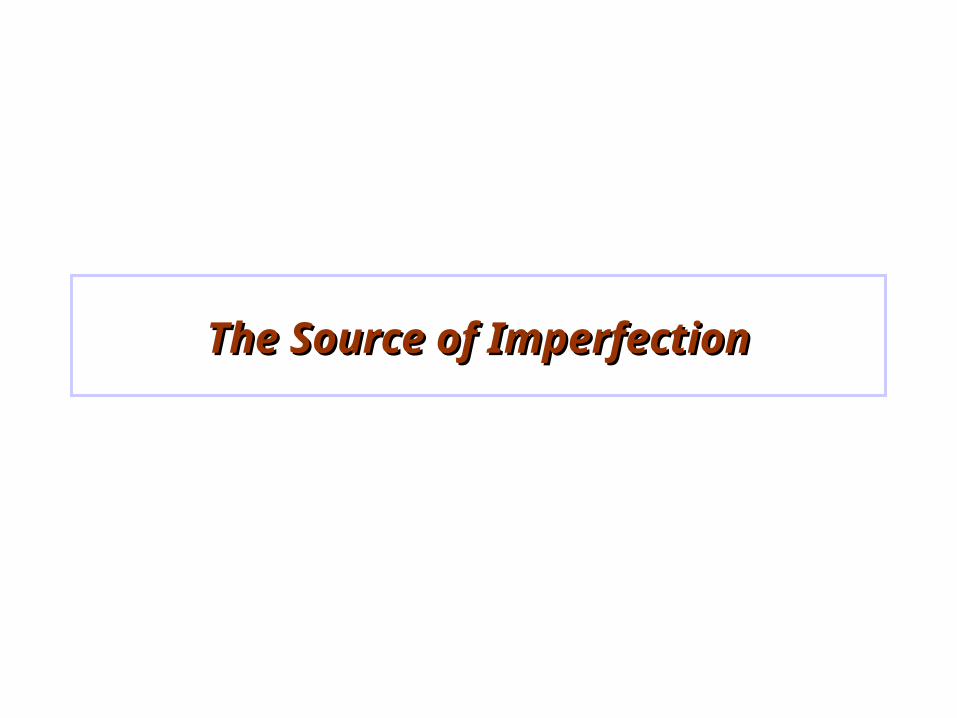
The Source of ImperfectionThe Source of Imperfection
General systems with Delamination or Buckle
-Highly compressed film DLC or Diamond film on glass / Si
Gold on copper film on sapphire Amorphous (hydrogenated ) Si film on glass/Si
Stainless steel on polycarbonate Thermal Barrier Coatings system
Imperfection deriven Delamination Buckle deriven Delamination
Introduction of Interface delaminationIntroduction of Interface delamination
Interface delamination on Diamond-Like Carbon film

The reflection of Small defects on the film surface after deposition
Large defects
Imperfection I – Interface defectsImperfection I – Interface defects
4 m 10 m 10 m
10 m 10 m 10 m 20 m

t=1 sect=5 sec
Free edge effect on delamination
Delamination sequence from free edge ( t = Real time)
Imperfection II - Free edgeImperfection II - Free edge
5 m 50 m
200 m 10 m
Thickness of film h= 0.13 m h= 0.80 m
Free edge

“Substrate curvature plays a role of imperfection”J. W. Hutchinson, JMPS, 49, 2001
b2 / Rh
Imperfection III – Substrate Curvature effectImperfection III – Substrate Curvature effect
> 1 The condition of Preferred
Propagation direction
Concave : axial Convex : circumferential

Observation on defect siteObservation on defect site

Deposition with CVD Diamond-like carbon films on glass substrates by PECVD with CH4 and C6H6 plus N2,
Negative self bias voltage : -100 to -700V
The film thickness : 0.13 ~ 0.46m Residual compression : 1GPa and 3GPa resulting in telephone cord buckles.
AFM In tapping mode (Digital Instrument company). Images of representative buckles and cross sectional profiles
FIB Dual-Beam FIB (FEI Company, DB235). Direct cut along the buckle (damage free) To create the straight-sided buckle from telephone cord buckle.
AES Auger Electron Spectroscopy Chemical analysis on several defect sites
Experiments on defect effectsExperiments on defect effects

Cross sections of defect sites - AFMCross sections of defect sites - AFM
Surface topology
Profile of Cross section

Cross sectioning : small defect - FIBCross sectioning : small defect - FIB
Defect Geometry
Thickness of film h ~ 0.46m
Wavelength : 10 mAmplitude : ~0.9 h
Before cut
After cut
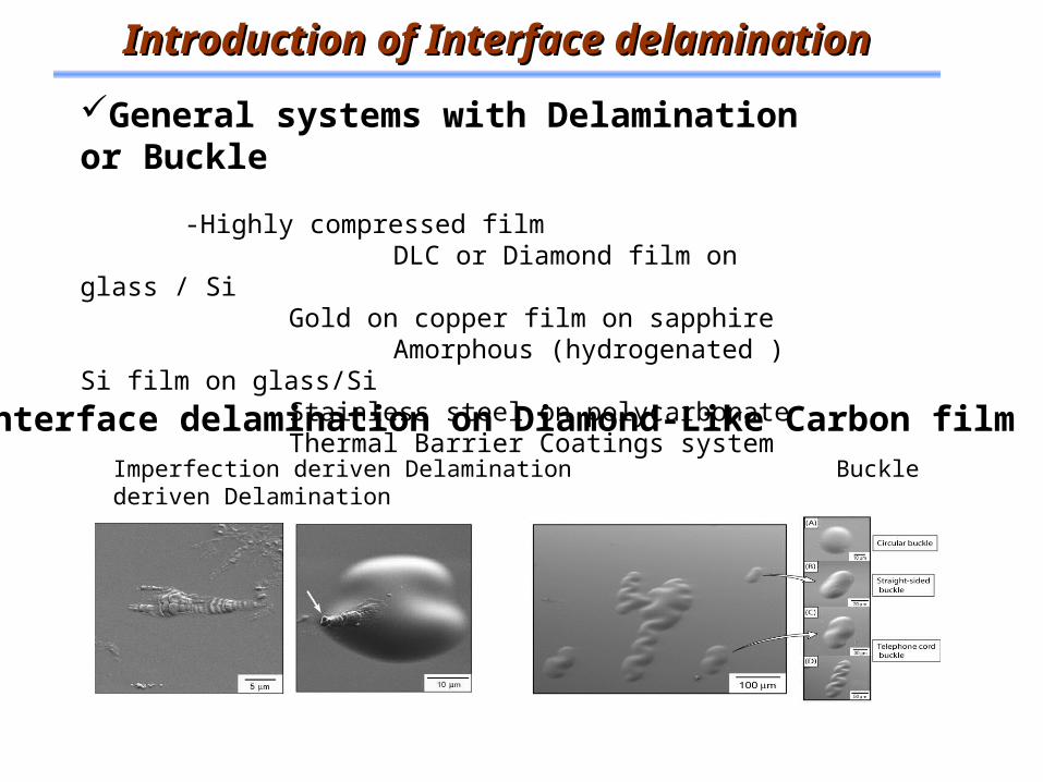
Cross sectioning : Large defect - FIBCross sectioning : Large defect - FIB
Defect Geometry
Thickness of film h ~ 0.46m
Wavelength : 40 m Amplitude : ~ 1.6 h
Before cut
After cut
Moon et al, Acta Mater., 2002

- Auger electron spectroscopy-
Film surface(Refection of defect)
Chemical analysis underneath defect sites -AESChemical analysis underneath defect sites -AES
Underneath film(Defect on substrate)
5 m 10 m

Discussion and SummaryDiscussion and Summary

Energy release rate with imperfection sizeEnergy release rate with imperfection size
Hutchinson, He, Evans, 2000, JMPS
iG min
The condition ofDelamination propagation

Lc
h11
int
R h
E R
3/2
Sub-critical No delamination
Stationary Delamination only
Super-critical Propagation of delamination
Summary of Observation on defect sitesSummary of Observation on defect sites
2/8* mJGlass
* Weiderhorn, S. M., J. Am. Ceram. Soc., 1967, 50, 407.
E=90~100GPa
R =1.9GPa
h 0.46m
.

•The source of imperfection on the interface
Defect, Free edge, and substrate curvature effect
•The characterization of Defect AFM :Measurement of Profile of defect on the film surface FIB : Cross sectional analysis with fine AES : Chemical analysis on foreign defect on the interface
•The condition of Defect-induced delamination
Lc
h11
int
R h
E R
3/2
SummarySummary