An Analytical Approach to Efficient Circuit Variability ... · An Analytical Approach to...
72
An Analytical Approach to Efficient Circuit Variability Analysis in Scaled CMOS Design by Samatha Gummalla A Thesis Presented in Partial Fulfillment of the Requirements for the Degree Master of Science Approved May 2011 by the Graduate Supervisory Committee: Chaitali Chakrabarti, Co-Chair Yu Cao, Co-Chair Bertan Bakkaloglu ARIZONA STATE UNIVERSITY December 2011
Transcript of An Analytical Approach to Efficient Circuit Variability ... · An Analytical Approach to...

An Analytical Approach to Efficient Circuit Variability Analysis
in Scaled CMOS Design
by
Samatha Gummalla
A Thesis Presented in Partial Fulfillmentof the Requirements for the Degree
Master of Science
Approved May 2011 by theGraduate Supervisory Committee:
Chaitali Chakrabarti, Co-ChairYu Cao, Co-ChairBertan Bakkaloglu
ARIZONA STATE UNIVERSITY
December 2011
ABSTRACT
Process variations have become increasingly important for scaled technologies starting
at 45nm. The increased variations are primarily due to random dopant fluctuations, line-edge
roughness and oxide thickness fluctuation. These variations greatly impact all aspects of circuit
performance and pose a grand challenge to future robust IC design. To improve robustness, ef-
ficient methodology is required that considers effect of variations in the design flow. Analyzing
timing variability of complex circuits with HSPICE simulations is very time consuming. This
thesis proposes an analytical model to predict variability in CMOS circuits that is quick and
accurate.
There are several analytical models to estimate nominal delay performance but very
little work has been done to accurately model delay variability. The proposed model is com-
prehensive and estimates nominal delay and variability as a function of transistor width, load
capacitance and transition time. First, models are developed for library gates and the accuracy
of the models is verified with HSPICE simulations for 45nm and 32nm technology nodes. The
difference between predicted and simulated σ/µ for the library gates is less than 1%. Next,
the accuracy of the model for nominal delay is verified for larger circuits including ISCAS’85
benchmark circuits. The model predicted results are within 4% error of HSPICE simulated re-
sults and take a small fraction of the time, for 45nm technology. Delay variability is analyzed
for various paths and it is observed that non-critical paths can become critical because of Vth
variation. Variability on shortest paths show that rate of hold violations increase enormously
with increasing Vth variation.
i

To my husband Ajith and my friend Gayathri
ii

ACKNOWLEDGEMENTS
I would like to express my gratitude and sincere thanks to my advisors Dr. Chaitali
Chakrabarti and Dr. Yu Cao for their continuous support and guidance, during the course of the
work. I am grateful to Dr. Bertan Bakkaloglu for agreeing to be on my defense committee and
for his time and efforts in reviewing my work.
I would like to thank all the members of our lab for their support and encouragement
in finishing the thesis. Finally, I take this opportunity to thank my parents, family and friends
who have been my pillars of strength through out my career, and who helped me become who
I am today.
I gratefully acknowledge the financial support from NSF through CSR0910699.
iii

TABLE OF CONTENTS
Page
LIST OF TABLES . . . . . . . . . . . . . . . . . . . . . . . . . . . . . . . . . . . . . vi
LIST OF FIGURES . . . . . . . . . . . . . . . . . . . . . . . . . . . . . . . . . . . . . vii
CHAPTER . . . . . . . . . . . . . . . . . . . . . . . . . . . . . . . . . . . . . . . . . 1
1 INTRODUCTION . . . . . . . . . . . . . . . . . . . . . . . . . . . . . . . . . . . 1
1.1 Motivation . . . . . . . . . . . . . . . . . . . . . . . . . . . . . . . . . . . . . 1
1.2 Existing Work . . . . . . . . . . . . . . . . . . . . . . . . . . . . . . . . . . . 1
1.3 Contributions . . . . . . . . . . . . . . . . . . . . . . . . . . . . . . . . . . . 2
1.4 Thesis Organization . . . . . . . . . . . . . . . . . . . . . . . . . . . . . . . . 3
2 VARIABILITY AND RELIABILITY ANALYSIS . . . . . . . . . . . . . . . . . . 4
2.1 Background . . . . . . . . . . . . . . . . . . . . . . . . . . . . . . . . . . . . 4
2.2 Variability in Circuit Performance . . . . . . . . . . . . . . . . . . . . . . . . 7
2.2.1 Case Study - Inverter . . . . . . . . . . . . . . . . . . . . . . . . . . . 7
2.2.2 Case Study - 6T-SRAM . . . . . . . . . . . . . . . . . . . . . . . . . 9
2.3 Effect of Variability on Path length . . . . . . . . . . . . . . . . . . . . . . . . 13
2.4 Effect of Variation on Logic Style . . . . . . . . . . . . . . . . . . . . . . . . 16
2.5 Variability and Logical Effort . . . . . . . . . . . . . . . . . . . . . . . . . . . 18
3 ANALYTICAL MODEL FOR NOMINAL DELAY . . . . . . . . . . . . . . . . . . 20
3.1 Nominal Delay Model for Inverter . . . . . . . . . . . . . . . . . . . . . . . . 20
3.1.1 Model derivation . . . . . . . . . . . . . . . . . . . . . . . . . . . . . 21
3.1.2 Model Validation . . . . . . . . . . . . . . . . . . . . . . . . . . . . . 24
3.2 Nominal Delay Model for NAND and NOR gates . . . . . . . . . . . . . . . . 26
3.2.1 NAND2 Delay Model . . . . . . . . . . . . . . . . . . . . . . . . . . 26
3.2.2 Model Validation . . . . . . . . . . . . . . . . . . . . . . . . . . . . . 30
3.2.3 NAND3 Delay Model . . . . . . . . . . . . . . . . . . . . . . . . . . 33
3.2.4 NAND3 Validation . . . . . . . . . . . . . . . . . . . . . . . . . . . . 34
3.2.5 Summary: . . . . . . . . . . . . . . . . . . . . . . . . . . . . . . . . . 35
4 ANALYTICAL MODEL FOR DELAY VARIABILITY . . . . . . . . . . . . . . . . 38
4.1 Delay Variability in Inverter . . . . . . . . . . . . . . . . . . . . . . . . . . . 38
4.2 Delay Variability in NAND2 and NOR2 gates . . . . . . . . . . . . . . . . . . 42iv
4.3 Delay Variability in NAND3 . . . . . . . . . . . . . . . . . . . . . . . . . . . 44
5 MODEL VALIDATION . . . . . . . . . . . . . . . . . . . . . . . . . . . . . . . . . 50
5.1 Small Circuits . . . . . . . . . . . . . . . . . . . . . . . . . . . . . . . . . . . 50
5.2 Application to ISCAS Benchmark Circuits . . . . . . . . . . . . . . . . . . . . 52
5.2.1 Effects of Variability . . . . . . . . . . . . . . . . . . . . . . . . . . . 54
6 CONCLUSIONS . . . . . . . . . . . . . . . . . . . . . . . . . . . . . . . . . . . . 58
6.1 Summary . . . . . . . . . . . . . . . . . . . . . . . . . . . . . . . . . . . . . 58
6.2 Future Work . . . . . . . . . . . . . . . . . . . . . . . . . . . . . . . . . . . . 59
REFERENCES . . . . . . . . . . . . . . . . . . . . . . . . . . . . . . . . . . . . . . . 60
v

LIST OF TABLES
Table Page
2.1 Minimum length, VDD, and p-n ratios of inverter for different technologies. . . . . . 8
2.2 SRAM transistor widths when length is taken to be minimum. . . . . . . . . . . . 10
2.3 Nominal delay and delay variation when AND6 is implemented in different styles
at 45nm technology node. . . . . . . . . . . . . . . . . . . . . . . . . . . . . . . . 17
2.4 Nominal delay and delay variation when AND6 is implemented in different styles
at 12nm technology node. . . . . . . . . . . . . . . . . . . . . . . . . . . . . . . . 18
2.5 Nominal delay and delay variation of buffer stage driving 1pf load with different
number of stages at 12nm technology node. . . . . . . . . . . . . . . . . . . . . . 19
3.1 Parameters used in the model and their extraction information. . . . . . . . . . . . 37
4.1 Variation numbers when input is given to top(M1) and bottom(M2) transistors of
NAND2 gate, with Vth of one of them varying. . . . . . . . . . . . . . . . . . . . . 44
4.2 Variation numbers when input is given to top(M1), middle(M2) and bottom(M3)
transistors of NAND3 gate, with Vth of one of them varying. . . . . . . . . . . . . 47
5.1 XOR2 gate nominal delay and delay variation values from HSPICE simulations
and model estimates. . . . . . . . . . . . . . . . . . . . . . . . . . . . . . . . . . 50
5.2 Full Adder nominal delay and delay variation values from simulated results and
model estimated results. . . . . . . . . . . . . . . . . . . . . . . . . . . . . . . . . 52
5.3 Comparison of nominal delay estimation for all the ISCAS’85 benchmark circuits. 53
5.4 Variation prediction for critical paths in ISCAS’85 benchmark circuits . . . . . . . 54
vi

LIST OF FIGURES
Figure Page
2.1 Effect of inter-die and intra-die variations in NAND2-RO delay, at different tech-
nologies. . . . . . . . . . . . . . . . . . . . . . . . . . . . . . . . . . . . . . . . . 5
2.2 Effect of inter-die and intra-die variations in 6T-SRAM DRV, at different technologies. 5
2.3 Schematic of 7-inverter chain. . . . . . . . . . . . . . . . . . . . . . . . . . . . . 8
2.4 Inverter: Mean delay and sigma as percentage of mean delay. . . . . . . . . . . . . 8
2.5 Inverter delay variation due to each intrinsic factor. . . . . . . . . . . . . . . . . . 9
2.6 Schematic of 6T-SRAM circuit. . . . . . . . . . . . . . . . . . . . . . . . . . . . 10
2.7 SRAM: Comparison of access time PDF’s in 45nm, 22nm, and 12nm technologies. 11
2.8 SRAM. Mean and 3σ point for all technologies . . . . . . . . . . . . . . . . . . . 11
2.9 SRAM RNM variability due to each intrinsic factor variation. . . . . . . . . . . . . 13
2.10 Nominal Delay and Delay variation with different path lengths at 45nm technology
node at (a) nominal voltage of VDD=1.0V, (b) VDD=0.5V. . . . . . . . . . . . . . . 14
2.11 Nominal Delay and Delay variation with different path lengths at 22nm technology
at (a) nominal voltage of VDD=0.8V, (b) VDD=0.5V. . . . . . . . . . . . . . . . . . 14
2.12 Nominal Delay and Delay variation with different path lengths at 12nm technology
at (a) nominal voltage of VDD=0.65V, (b) VDD=0.5V . . . . . . . . . . . . . . . . . 15
2.13 Different implementations of AND6 function. . . . . . . . . . . . . . . . . . . . . 17
2.14 Buffer loaded with 1pF capacitance. . . . . . . . . . . . . . . . . . . . . . . . . . 18
3.1 NMOS characteristics - Simulated and Analytical . . . . . . . . . . . . . . . . . . 21
3.2 Schematic of CMOS Inverter circuit. . . . . . . . . . . . . . . . . . . . . . . . . . 21
3.3 Regions of operation of NMOS transistor as input rises. . . . . . . . . . . . . . . . 22
3.4 Inverter HL delay with varying width, capacitance, transition time at 45nm tech-
nology node. . . . . . . . . . . . . . . . . . . . . . . . . . . . . . . . . . . . . . 25
3.5 Inverter HL delay with varying width, capacitance, transition time at 32nm tech-
nology node. . . . . . . . . . . . . . . . . . . . . . . . . . . . . . . . . . . . . . 25
3.6 Inverter LH delay with varying width, capacitance, transition time at 45nm tech-
nology node. . . . . . . . . . . . . . . . . . . . . . . . . . . . . . . . . . . . . . 26
3.7 Inverter LH delay with varying width, capacitance, transition time at 32nm tech-
nology node. . . . . . . . . . . . . . . . . . . . . . . . . . . . . . . . . . . . . . 27vii

Figure Page3.8 NAND2 gate schematics. . . . . . . . . . . . . . . . . . . . . . . . . . . . . . . . 27
3.9 NAND2 gate discharge behavior when input is given to bottom transistor. . . . . . 28
3.10 NAND2 gate HL delay with varying width, capacitance, transition time when input
is given to M2 at 45nm technology node. . . . . . . . . . . . . . . . . . . . . . . . 30
3.11 NAND2 gate HL delay with varying width, capacitance, transition time when input
is given to M1 at 45nm technology node. . . . . . . . . . . . . . . . . . . . . . . . 31
3.12 NOR2 gate LH delay with varying width, capacitance, transition time when input
is given to bottom PMOS at 45nm technology node. . . . . . . . . . . . . . . . . . 32
3.13 NOR2 gate LH delay with varying width, capacitance, transition time when input
is given to top PMOS at 45nm technology node. . . . . . . . . . . . . . . . . . . . 32
3.14 NAND3 gate schematics. . . . . . . . . . . . . . . . . . . . . . . . . . . . . . . . 33
3.15 NAND3 gate HL delay with varying width, capacitance, transition time when input
is given to M1 at 45nm technology node. . . . . . . . . . . . . . . . . . . . . . . . 35
3.16 NAND3 gate HL delay with varying width, capacitance, transition time when input
is given to M2 at 45nm technology node. . . . . . . . . . . . . . . . . . . . . . . . 36
3.17 NAND3 gate HL delay with varying width, capacitance, transition time when input
is given to M3 at 45nm technology node. . . . . . . . . . . . . . . . . . . . . . . . 36
4.1 Inverter HL delay variation with varying (a) width, (b) capacitance, (c) transition
time at 45nm technology node. . . . . . . . . . . . . . . . . . . . . . . . . . . . . 39
4.2 Inverter HL delay variation with varying (a)width, (b)capacitance, (c)transition
time at 32nm technology node. . . . . . . . . . . . . . . . . . . . . . . . . . . . . 40
4.3 Inverter LH delay variation with varying width, capacitance, transition time at
45nm technology node. . . . . . . . . . . . . . . . . . . . . . . . . . . . . . . . . 41
4.4 Inverter LH delay variation with varying width, capacitance, transition time at
32nm technology node. . . . . . . . . . . . . . . . . . . . . . . . . . . . . . . . . 41
4.5 NAND2 gate HL delay variation with varying width, capacitance, transition time
when input is given to M2 at 45nm technology node. . . . . . . . . . . . . . . . . 45
4.6 NAND2 gate HL delay variation with varying width, capacitance, transition time
when input is given to M1 at 45nm technology node. . . . . . . . . . . . . . . . . 45
viii

Figure Page4.7 NAND3 gate HL delay variation with varying width, capacitance, transition time
when input is given to M1 at 45nm technology node. . . . . . . . . . . . . . . . . 48
4.8 NAND3 gate HL delay variation with varying width, capacitance, transition time
when input is given to M2 at 45nm technology node. . . . . . . . . . . . . . . . . 48
4.9 NAND3 gate HL delay variation with varying width, capacitance, transition time
when input is given to M3 at 45nm technology node. . . . . . . . . . . . . . . . . 49
5.1 Schematic of XOR2 circuit . . . . . . . . . . . . . . . . . . . . . . . . . . . . . . 51
5.2 XOR2 gate with input and output loading with FO4. . . . . . . . . . . . . . . . . . 51
5.3 Mirror Adder structure of Full Adder . . . . . . . . . . . . . . . . . . . . . . . . . 52
5.4 Full Adder with input and output loading with FO4. . . . . . . . . . . . . . . . . . 52
5.5 Delay distribution curve for C880 benchmark circuit at nominal and with variations. 55
5.6 Non-critical path becoming critical in light of Vth variation. . . . . . . . . . . . . . 56
5.7 Number of paths that can cause hold time violations because of Vth variations in (a)
C5315, (b) C2670, ISCAS benchmark circuit at 45nm technology node. . . . . . . 57
ix
Chapter 1
INTRODUCTION
1.1 Motivation
As CMOS technology nodes move to 45nm and below, process variations increase significantly.
This causes high variability in circuit performance and also reduces manufacturing yield. Var-
ious techniques like global back gate biasing and adaptive VDD have been proposed to reduce
variation [10, 5]. But these techniques can correct only small amounts of variation. To improve
manufacturing yield of technologies 45nm and below, performance variability should be con-
sidered during the design phase. In the conventional design approach, high variability leads
to over designing, thereby increasing area and power consumption. To avoid over designing,
accurate estimation of variability is required. Estimating variability in complex circuits using
HSPICE is impractical because of large simulation time for even moderate sized circuits. Also
number of paths to be analyzed increase with complexity of the circuit and it becomes practi-
cally impossible to analyze all of them with HSPICE simulations.
In this thesis, an analytical model has been proposed to accurately predict variability for
any number of paths. While there are many analytical models [25, 26, 31] to predict nominal
delays, these models do not analyze effect of process variations, which is critical for future
technology nodes. The existing work on variability analysis are either not accurate [6] or do not
provide analytical models for fast estimation [20]. In contrast, this thesis proposes a model that
is very accurate and provides a fast way to analyze variability in complex CMOS circuits.
1.2 Existing Work
Estimating delay analytically is important in circuit design because it gives insights into the
factors affecting delay and gives the designer better control over the design. Of all the models
for delay estimation, Shockley’s model [25] is the most widely used one. But for submicron
technologies, Shockley’s delay model is not accurate because it does not consider the effect of
velocity saturation. Sakurai and Newton’s [26] α-power model, on the other hand, considers
velocity saturation and is simple and accurate. But the α-power law model does not consider
channel length modulation. Current equations considering channel length modulation have been
developed in [21]. The corresponding delay model considers gate to drain coupling capacitance
1

and short circuit current, and are unnecessarily complicated. The delay model is in [31] for
inverter also considers channel length modulation but is also complex because of considering
gate to drain coupling capacitance and sub-threshold current.
There are very few models for delay variation. An analytical model for delay variation
is derived in [6] where the nominal delay equations are based the α-power model. Here gates
with stacked transistors are simplified to equivalent inverters, so variation because of different
inputs cannot be characterized. There is another piece of work [20] that characterizes delay
variations, but no analytical equations are derived to model the variation.
1.3 Contributions
The objective of this thesis is to develop an accurate analytical model for predicting nominal
delay and delay variability for scaled technologies. First, nominal delay model for inverter
is developed at 45nm technology node. The model is developed based on accurate current
equations that take channel length modulation into consideration. All the factors affecting delay,
namely, transistor widths, load capacitance(CL) and input slew rate(tr) are considered in the
model. The analytical model matches with the HSPICE simulated results closely for both high
to low(HL) and low to high(LH) delays. The inverter delay model is applied to 32nm technology
and here too the model shows very good agreement with HSPICE simulated results.
The nominal delay model is then extended to consider effect of stacked transistors in
NAND and NOR gates. It is observed that the delay depends on the position of the transistor
with switching input. Specifically transistors in between transistor with switching input and
output node contribute to delay, while transistors in between transistor with switching input and
supply nodes do not have any effect. This feature is taken into account while deriving a model
for nominal delay for gates with stacked transistors. The proposed model is very accurate and
matches HSPICE simulated results for NAND and NOR gates at 45nm technology node.
Next, delay variation because of variations in threshold voltage(Vth) is analyzed. The
proposed model for delay variation not only considers Vth variation, but also its dependency on
other factors such as CL and tr. The variability model is extended to NAND and NOR gates and
the variation in each transistor is analyzed separately. The variability model for inverter, NAND
and NOR gates closely matches HSPICE simulated results.
2

The nominal delay model and variability model are then applied to complex gates like
XOR and Full Adder and the results are compared with HSPICE simulated results. Finally, the
model is applied to complex ISCAS’85 benchmark circuits and the results are compared with
Synopsys primetime estimated values using 45nm Nangate library [3]. The number of gates in
critical paths range from 12-124 in these benchmark circuits. For these critical paths, estimated
nominal delay values matches the Synopsys predicted delay within 4% error. The variability
in delay is also predicted for these circuits. The predicted σ/µ for all the critical paths is less
than 3% when Vth variation of 50mV is given for transistor of width twice minimum length at
45nm technology. With varying σVth some important trends are demonstrated regarding setup
and hold times. It is observed that non-critical paths would become critical and rate of hold
violations increases enormously with increasing σVth .
1.4 Thesis Organization
Chapter 2 discusses the variability trends with CMOS technology scaling. Variability is ana-
lyzed for varying path lengths, logic implementation style and sizing based on logical effort.
Chapter 3 gives the derivation of nominal delay for inverter and its extension to NAND and
NOR gates. The model is verified with HSPICE results. Chapter 4 derives the delay variability
equations due to threshold voltage variations for inverter NAND and NOR gates. The model
estimated results match the HSPICE simulated results quite closely. The proposed model is
verified for XOR2 and Full Adder circuits at 45nm technology in Chapter 5. The model is
also used to estimate the delay of complex ISCAS’85 benchmark circuits and the results are
compared with Synopsys ptimetime estimated values using 45nm library [3]. The use of the
proposed model into the design flow is also demonstrated. It is shown how possible timing
errors due to variability can be easily identified. Chapter 6 concludes the work.
3
Chapter 2
VARIABILITY AND RELIABILITY ANALYSIS
Variability in circuit performance increases with technology scaling because of increasing thresh-
old voltage variations. This chapter begins with the classification of variation and causes of
variation in threshold voltage of transistors (Section 2.1). This is followed by an analysis of
variability trends with technology scaling in gates like inverter, AND6 and circuits like inverter
chain, 6-T SRAM (Section 2.2). A mechanism to reduce variability by increasing the length
of transistor is also presented here. Variability dependency on factors like path length (Section
2.3), differences in implementations of the same logic function (Section 2.4) and logical effort
sizing are also studied (Section 2.5).
2.1 Background
CMOS scaling is advancing towards the 10nm regime [2]. Such aggressive scaling inevitably
leads to vastly increased variability in circuit performance, posing a grand challenge to future
robust IC design.
Classification of variations: Threshold voltage variations in CMOS can be divided into inter-
die variations and intra-die variations. Inter-die variations are systematic variations and affect
adjacent transistors on a chip with equal shift from nominal value. Intra-die variations are ran-
dom variations and affect adjacent transistors on same chip with different shifts. Inter-die vari-
ations can be adjusted by adapting the supply voltage, VDD to compensate for shifted threshold
voltage [15]. Forward and reverse-body bias techniques can also be used [9, 17, 15] to com-
pensate for inter-die variations. Inter-die variations affect variability in combinational circuits
more than sequential circuits.
Intra-die variations are more difficult to solve because these variations are not system-
atic. However the variations reduce because of averaging effect with increasing path length. In
conventional circuit design techniques, transistors in non-critical paths are replaced with high-
Vth transistors to reduce leakage power. But this technique increases the delay of non-critical
paths and these non-critical paths can become critical paths because of Vth variation. Hence
conventional design techniques to reduce power cannot be directly applied to future technology
designs as power and variability pose opposite constraints [18].
4

1 2 n m 1 6 n m 2 2 n m 3 2 n m 4 5 n m
1 . 2 x 1 0 - 1 0
1 . 4 x 1 0 - 1 0
1 . 6 x 1 0 - 1 0
1 . 8 x 1 0 - 1 0
2 . 0 x 1 0 - 1 0
2 . 2 x 1 0 - 1 0
Delay
T e c h n o l o g y n o d e
N o m i n a l I n t e r - d i e v a r i a t i o n s I n t r a - d i e v a r i a t i o n s
Figure 2.1: Effect of inter-die and intra-die variations in NAND2-RO delay, at different tech-nologies.
1 2 n m 1 6 n m 2 2 n m 3 2 n m 4 5 n m0 . 0 50 . 1 00 . 1 50 . 2 00 . 2 50 . 3 00 . 3 50 . 4 00 . 4 50 . 5 00 . 5 50 . 6 00 . 6 50 . 7 0
DRV(
V)
T e c h n o l o g y n o d e
N o m i n a l D R V I n t e r - d i e v a r i a t i o n s I n t r a - d i e v a r i a t i o n s
Figure 2.2: Effect of inter-die and intra-die variations in 6T-SRAM DRV, at different technolo-gies.
5
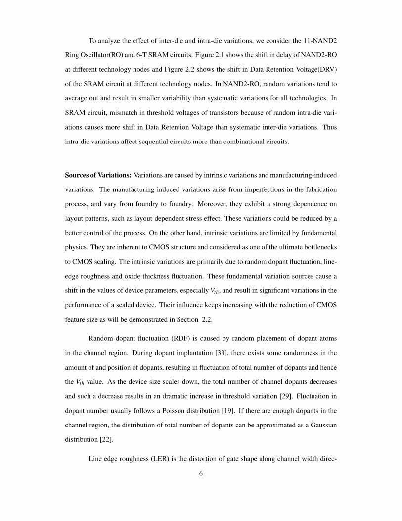
To analyze the effect of inter-die and intra-die variations, we consider the 11-NAND2
Ring Oscillator(RO) and 6-T SRAM circuits. Figure 2.1 shows the shift in delay of NAND2-RO
at different technology nodes and Figure 2.2 shows the shift in Data Retention Voltage(DRV)
of the SRAM circuit at different technology nodes. In NAND2-RO, random variations tend to
average out and result in smaller variability than systematic variations for all technologies. In
SRAM circuit, mismatch in threshold voltages of transistors because of random intra-die vari-
ations causes more shift in Data Retention Voltage than systematic inter-die variations. Thus
intra-die variations affect sequential circuits more than combinational circuits.
Sources of Variations: Variations are caused by intrinsic variations and manufacturing-induced
variations. The manufacturing induced variations arise from imperfections in the fabrication
process, and vary from foundry to foundry. Moreover, they exhibit a strong dependence on
layout patterns, such as layout-dependent stress effect. These variations could be reduced by a
better control of the process. On the other hand, intrinsic variations are limited by fundamental
physics. They are inherent to CMOS structure and considered as one of the ultimate bottlenecks
to CMOS scaling. The intrinsic variations are primarily due to random dopant fluctuation, line-
edge roughness and oxide thickness fluctuation. These fundamental variation sources cause a
shift in the values of device parameters, especially Vth, and result in significant variations in the
performance of a scaled device. Their influence keeps increasing with the reduction of CMOS
feature size as will be demonstrated in Section 2.2.
Random dopant fluctuation (RDF) is caused by random placement of dopant atoms
in the channel region. During dopant implantation [33], there exists some randomness in the
amount of and position of dopants, resulting in fluctuation of total number of dopants and hence
the Vth value. As the device size scales down, the total number of channel dopants decreases
and such a decrease results in an dramatic increase in threshold variation [29]. Fluctuation in
dopant number usually follows a Poisson distribution [19]. If there are enough dopants in the
channel region, the distribution of total number of dopants can be approximated as a Gaussian
distribution [22].
Line edge roughness (LER) is the distortion of gate shape along channel width direc-
6
tion [33]. This variation is mainly affected by the process of gate etching, and is inherent to
gate materials [23, 7, 14, 12]. The concerning fact is that LER variation does not scale with
technology and the improvement in the lithography process does not effectively reduce such an
intrinsic variation. Numerical simulations and silicon data further indicate that the LER effect
significantly increases the leakage and threshold variations.
Oxide Thickness Fluctuation (OTF) is caused by the atom scale surface roughness of
the Si-SiO2 and Gate-SiO2 interfaces [8]. When oxide thickness is equivalent to only a few
silicon atom layers, the atomic scale interface roughness steps result in significant oxide thick-
ness variation [16]. The unique random pattern of the gate oxide thickness and interface land-
scape makes each MOSFET different from its counterparts and leads to variations in the surface
roughness. This affects mobility, gate tunnelling current [30, 11] and hence threshold voltage
variation from device to device.
2.2 Variability in Circuit Performance
The variations in Vth are applied to two benchmark circuits - inverter chain and 6T-SRAM, and
the variability in their performance is quantified. For the inverter chain, the performance metric
is chosen to be delay and for 6T SRAM, the performance metrics are read access time and read
noise margin (RNM).
2.2.1 Case Study - Inverter
An inverter chain is built with seven inverters as shown in Figure 2.3. Delay measurements
are made across the fourth inverter, because it is isolated from both input and output loading
effects [2]. Length of both PMOS and NMOS is kept at the minimum feature size of the specific
technology. Width of NMOS is taken to be 8 times the minimum length. Width of PMOS is
found so that rise and fall times are equal. Table 2.1 shows p− n ratios for technologies from
45nm to 12nm. These are the p−n ratios used throughout this work.
100 Monte Carlo simulations are run by adding independent variation in Vth for all
fourteen transistors in the inverter chain. Figure 2.4 shows the trend in nominal delay and
delay variations with technology scaling. As seen from the Figure 2.4, delay decreases with
scaling but variability, as a percentage of mean, increases rapidly because of increasing Vth
7

NOT NOT NOT NOT NOT NOTNOT
Figure 2.3: Schematic of 7-inverter chain.
Technology L(nm) VDD (V) p-n ratio45nm 45 1.0 1.0232nm 32 0.9 0.9622nm 22 0.8 0.9116nm 16 0.7 0.8012nm 12 0.65 0.84
Table 2.1: Minimum length, VDD, and p-n ratios of inverter for different technologies.
variation. This implies that technology scaling assures improved nominal performance but
when variability is considered, it degrades the robustness of the circuit.
Figure 2.4: Inverter: Mean delay and sigma as percentage of mean delay.
Further, the contribution of individual intrinsic factors, namely, RDF, LER and OTF, to-
wards delay is analyzed. This is done by applying Vth variation because of each of these factors
to the inverter circuit. The variation in Vth is calculated using the method in [32] . Figure 2.5
illustrates the contribution of RDF, LER and OTF for different technology nodes. LER and OTF8

are the major contributors to variability in lower technology nodes. The impact of LER on Vth
variation is mainly because of fluctuation of channel length in the gate width direction, which
is also called gate line-width roughness (LWR) [24]. The channel length fluctuation combined
with severe short channel effect contributes to a large Vth variation. OTF causes the fluctuation
of gate voltage drop across oxide layer, and further results in Vth variation. This effect becomes
pronounced during scaling because height of the atomic layer at oxide surface does not scale
with the oxide thickness. Therefore, the average fluctuation becomes larger as the area of gate
oxide scales.
1 2 n m 1 6 n m 2 2 n m 3 2 n m 4 5 n m0 . 0
2 . 0 x 1 0 - 1 3
4 . 0 x 1 0 - 1 3
6 . 0 x 1 0 - 1 3
Delay
(s)
T e c h n o l o g y
O T F L E R R D F
Figure 2.5: Inverter delay variation due to each intrinsic factor.
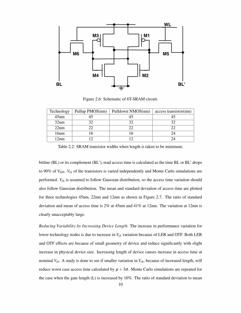
2.2.2 Case Study - 6T-SRAM
The effect of Vth variation on Read Access time and RNM are examined for a typical 6T-SRAM
cell shown in Figure 2.6. All the six transistors have minimum length for simplicity. The pull
up PMOS transistors are assigned minimum width. The widths of access transistor and pull
down NMOS are found by making the read and write noise margins equal [13]. The transistor
widths for all the technologies are given in Table 2.2.
Read Access Time: Read Access Time depends on sense amplifiers at the output of
SRAM circuit. Assuming that sense amplifiers are able to measure 10% of VDD drop on either9
M1
M2
M3
M4
M5M6
BL BL'
WL
Figure 2.6: Schematic of 6T-SRAM circuit.
Technology Pullup PMOS(nm) Pulldown NMOS(nm) access transistor(nm)45nm 45 45 4532nm 32 32 3222nm 22 22 2216nm 16 16 2412nm 12 12 24
Table 2.2: SRAM transistor widths when length is taken to be minimum.
bitline (BL) or its complement (BL’), read access time is calculated as the time BL or BL’ drops
to 90% of VDD. Vth of the transistors is varied independently and Monte Carlo simulations are
performed. Vth is assumed to follow Gaussian distribution, so the access time variation should
also follow Gaussian distribution. The mean and standard deviation of access time are plotted
for three technologies 45nm, 22nm and 12nm as shown in Figure 2.7. The ratio of standard
deviation and mean of access time is 2% at 45nm and 41% at 12nm. The variation at 12nm is
clearly unacceptably large.
Reducing Variability by Increasing Device Length: The increase in performance variation for
lower technology nodes is due to increase in Vth variation because of LER and OTF. Both LER
and OTF effects are because of small geometry of device and reduce significantly with slight
increase in physical device size. Increasing length of device causes increase in access time at
nominal Vth. A study is done to see if smaller variation in Vth, because of increased length, will
reduce worst case access time calculated by µ +3σ . Monte Carlo simulations are repeated for
the case when the gate length (L) is increased by 10%. The ratio of standard deviation to mean10

0 2 4 6 8 1 0
0 . 0
0 . 2
0 . 4
0 . 6
0 . 8
1 . 0
A c c e s s t i m e ( p s )
N o m i n a l L i n c r e a s e d1 2 n m
0 2 4 6 8 1 0
A c c e s s t i m e ( p s )
2 2 n m
0 2 4 6 8 1 0
A c c e s s t i m e ( p s )
4 5 n m
Figure 2.7: SRAM: Comparison of access time PDF’s in 45nm, 22nm, and 12nm technologies.
of access time drops to 28% at 12nm at the cost of slight reduction in nominal performance!
Figure 2.8: SRAM. Mean and 3σ point for all technologies
11

The simulation results show that at 45nm technology node, the performance variation
does not improve with increase in L. At 22nm, the variation decreases but is not large enough
to bring the 3σ access time less than the nominal. However at 12nm, the 3σ access time with
10% larger L is less than the nominal case. Figure 2.8 also shows that with scaling, while the
nominal access time reduces, the worst case delay increases. By tuning gate length to 10%
more than nominal, the access time increases for each technology but the trend with technology
scaling remains the same. The worst case delay at 12nm reduces below the nominal thus giving
tightly coupled performance variation than at nominal. As variation in performance is small in
current technologies, the focus of process tuning should be to enhance the nominal performance
but with scaling, variability becomes an important parameter.
Read Noise Margin(RNM): For a first order analysis, RNM is considered to be a linear
function of mismatches between Vth of transistors. The following six mismatches are considered
and all are taken to be independent.
1. Mismatch between M1,M2 and between M3,M4
2. Mismatch between M1,M3 and between M2,M4
3. Mismatch between M2,M5 and between M4,M6
The variations in Vth of each transistor are directly mapped to mismatches between
pairs as listed above. The variation of mismatch is considered to be summation of variation of
both transistors as given in equation below.
σ2Vth,(M1M2)
= σ2Vth,(M1)
+σ2Vth,(M2)
(2.1)
Threshold voltage of each transistor is changed separately and shift in RNM is observed. The β
coefficients are calculated empirically from linear equation between mismatch and RNM. The
variation in RNM is calculated from variation of mismatches and β coefficients as given in:
σ2RNM = β 2
1 σ2Vth,(M1M2)
+β 22 σ2
Vth,(M3M4)+β 2
3 σ2Vth,(M1M3)
+β 24 σ2
Vth,(M2M4)+β 2
5 σ2Vth,(M2M5)
+β 26 σ2
Vth,(M4M6)(2.2)
12

The variation due to the individual intrinsic parameters is calculated and is shown in
Figure 2.9. Similar to inverter delay variation, the contribution of LER and OTF on SRAM
RNM variation increases with technology scaling. The variation due to RDF dominates till
22nm, but below that, LER and OTF are the major contributors. The mean of RNM for 12nm
is 0.074V and from Figure 2.9 we can see that variability is very large. SRAM is very sensitive
to mismatches and its sensitivity increases significantly with scaling.
1 2 n m 1 6 n m 2 2 n m 3 2 n m 4 5 n m0 . 0 00 . 0 10 . 0 20 . 0 30 . 0 40 . 0 50 . 0 60 . 0 70 . 0 80 . 0 90 . 1 00 . 1 10 . 1 2
RNM(
V)
T e c h n o l o g y
O T F L E R R D F
Figure 2.9: SRAM RNM variability due to each intrinsic factor variation.
2.3 Effect of Variability on Path length
To evaluate variability of circuits, with different path lengths, a ring oscillator with 51 inverters
is considered. Delay across different number of gates is observed. As path length increases,
nominal delay increases in proportion to the number of gates in the path. Variation in threshold
voltage is considered to be Gaussian distributed and completely independent in each transistor.
So variation in delay is given by equation (2.3) [28] and increases with√
N, where N is the
number of stages.
σpath =√
∑σ2gate (2.3)
13

Figure 2.10: Nominal Delay and Delay variation with different path lengths at 45nm technology
node at (a) nominal voltage of VDD=1.0V, (b) VDD=0.5V.
Figure 2.11: Nominal Delay and Delay variation with different path lengths at 22nm technology
at (a) nominal voltage of VDD=0.8V, (b) VDD=0.5V.
14

Figure 2.12: Nominal Delay and Delay variation with different path lengths at 12nm technology
at (a) nominal voltage of VDD=0.65V, (b) VDD=0.5V
So overall, the worst case delay, µ +3σ keeps increasing with increasing path length.
But the variation in delay as a percentage of nominal delay, σ/µ , keeps decreasing. Figures 2.10
- 2.12 show these trends with increasing path length. Figure 2.10a shows nominal delay, worst
case delay (µ + 3σ ) and σ/µ of inverter chain at 45nm technology node at nominal voltage
of VDD=1.0V. Figure 2.10b plots the same at VDD=0.5V. Nominal delay for path length of 31
inverters is 277.9ps at nominal VDD=1.0V and 2104ps at VDD=0.5V. Delay variation(σ ) because
of threshold voltage variation calculated using the method in [32] is 1.329ps at nominal VDD
and 47.5ps at VDD = 0.5V . Thus variability(σ/µ%) increased from 0.47% at nominal VDD to
2.25% at lower VDD. This shows that variability becomes increasingly important for low power
applications, where supply voltage is reduced. Similar trends are observed for 22nm, 12nm at
nominal voltage and at VDD=0.5V as shown in Figures 2.11 and 2.12.
As both nominal delay and delay variation increase with increasing number of gates
in a path, worst case delay (µ + 3σ ) also keeps increasing. This trend can be clearly seen at
12nm technology node in Figure 2.12. At 12nm technology node, for nominal supply voltage,
15

when path length is 10, the difference between nominal and worst case delay curves (that is
3σ ) is 10.74ps and this difference increases to 27.55ps at path length of 47. Hence even though
random variations average out with increasing path length, path length cannot be increased to
reduce delay variation. But the delay variation with respect to nominal delay(σ/µ%) becomes
small with increasing path length. It reduces from 7.94% for path length of 10 inverters to
4.33% for path length of 47 at 12nm technology node.
Threshold voltage variations across technology nodes keeps increasing with technol-
ogy scaling. While delay variation increases, the nominal delay decreases and σ/µ increases
significantly. At nominal voltages, σ/µ at 45nm for path length of 43 inverters is 0.41%, while
it is 1.27% at 22nm and 4.5% at 12nm. Further VDD scaling at 22nm and 12nm technologies
increases σ/µ to 4.8% at 22nm and 10.93% 12nm. Such high values for even large path lengths
makes these circuits unreliable at scaled technologies.
2.4 Effect of Variation on Logic Style
Any logic function can be implemented in multiple ways. Figure 2.13 shows how large gates
like AND6 can be implemented in multiple ways. We study how variation may be affected
by the way a function is implemented using AND6 as an example. The first implementation
has 6 NMOS transistors stacked, so width of NMOS is 6Wn. The second implementation has
3 transistors stacked, so width is 3Wn. The third implementation has only two transistors in
stack and width is 2Wn. The final implementation has 3 stacked trnansistors and width is 3Wn.
Switching input in a stack is always given to the transistor farthest from output so that maximum
delay in the gate is considered. Low to high delay is considered as performance metric because
this triggers the stack in both NAND and NOR gates.
Variation in Vth is smallest in the first implementation, because σVth ∝1√W
and the first
implementation has the widest gate. Variation in delay relative to nominal delay is small in the
first case when compared to second and third implementations. But nominal delay value is high
for that implementation because of large stack. So worst case delay, µ + 3σ is large for first
case compared with all other implementations. For the fourth implementation, nominal delay
is large because of multiple stages but σ/µ is smaller than second and third implementations
because multiple stages average out the effect of random variations. Both second and third
16

NAND NOTNAND
NAND
NOR
NAND
NAND
NAND
NOR
NAND NOT
NAND NOT
NAND NOT
1 2
3 4
Figure 2.13: Different implementations of AND6 function.
implementations give almost the same delay and delay variability because both have similar
stacks and it is not clear as to which is better circuit.
The delay and delay variation results for 45nm technology are summarized in Table 2.3.
Table 2.4 shows similar trends for 12nm technology. So in all the implementations, circuits with
lower nominal delay gives lower variability. This is because variability depends on nominal
value along with amount of threshold voltage variation. This can be shown as follows. Delay
Tp ∝1ID
, and ID ∝ (VDD−Vth). From [28], we have
σTp =∂ (Tphl)
∂VthσVth (2.4)
Substituting we get,
σTP = σVth
∂TP
∂Vth= σVth
TP
VDD−Vth(2.5)
Implementation µ (ps) σ (ps) µ +3σ (ps) σ/µ %1 18.96 0.19 19.54 1.032 11.72 0.13 12.11 1.113 12.01 0.13 12.40 1.084 18.33 0.18 18.87 0.98
Table 2.3: Nominal delay and delay variation when AND6 is implemented in different styles at45nm technology node.
17

Implementation µ (ps) σ (ps) µ +3σ (ps) σ/µ %1 18.76 1.18 22.30 6.292 10.04 0.84 12.56 8.373 9.50 0.90 12.19 9.424 13.98 1.16 17.46 8.30
Table 2.4: Nominal delay and delay variation when AND6 is implemented in different styles at12nm technology node.
2.5 Variability and Logical Effort
A path which is sized according to logical effort can have
• fewer gates with high electrical effort per gate or
• more number of gates with low electrical effort per gate.
Longer paths with slowly increasing gate sizes should have lower variability than small
paths with rapidly increasing gate sizes. This is because in both cases, sizes are increasing
which decreases variation in Vth. But longer paths tend to average out effect of random varia-
tions so variation should be less. As an example, consider an inverter chain, loaded with 1pF
capacitance as shown in Figure 2.14. The first stage inverter is fixed to be 8 times minimum
size. The buffer stage is designed with different number of stages and gate sizing of each stage
is calculated through logical effort. The results are shown in Table 2.5 for 12nm technology
node.
1pF. . .
Figure 2.14: Buffer loaded with 1pF capacitance.
18

No. of Stages Fanout µ (ps) σ (ps) µ +3σ (ps)2 30 34.40 3.005 43.424 5 20.40 1.362 24.494 4 18.82 1.281 22.666 3 27.13 1.121 30.498 2 23.69 1.237 27.40
Table 2.5: Nominal delay and delay variation of buffer stage driving 1pf load with differentnumber of stages at 12nm technology node.
From Table 2.5, we see that fanout 4 has the least nominal delay. Variation in delay
should decrease when number of stages increases because of averaging out of random variations
and also because of increasing gate sizes that decreases Vth variation. But variability depends on
nominal delay also and nominal delay increases with increasing number of stages. Because of
these opposite trends, the variation for path lengths 4, 6 and 8 are almost the same. Increasing
nominal delay increases worst case(µ +3σ ) performance for path lengths 4, 6 and 8. For path
length of 2 inverters, nominal delay is high because of high load on each inverter and variability
is high because it is proportional to nominal delay. So it is best to design circuits with minimum
number of gates while keeping the nominal delay low.
19

Chapter 3
ANALYTICAL MODEL FOR NOMINAL DELAY
An analytical model for nominal delay is developed in this chapter. Delay equations are ini-
tially derived for CMOS inverter gate from current equations which consider short channel
effects [21] in Section 3.1. The model is quite detailed and accounts for width of gate, loading
capacitance and input transition time. The derivation is extended to account for stacked transis-
tors in NAND and NOR gates in Section 3.2. The analytical models are validated using PTM
models [4] at 45nm technology and 32nm technology nodes.
3.1 Nominal Delay Model for Inverter
The inverter delay models derived with current equations from Shockley’s MOSFET model or
Sakurai’s α-power law [27] do not apply as technology scales down below 50nm. This is be-
cause channel length modulation becomes important in scaled technologies and saturation cur-
rent is no longer constant. In fact, saturation current is a function of drain-source voltage(VDS).
The current equation for scaled devices has been derived in [21] and is given below.
ID =
0, (VGS ≤Vth : cuto f f ),
βl(Vin−Vth)αVDS, (VDS <VDSAT : linear),
βs(Vin−Vth)α [1+λ (VDS−VDD)], (VDS ≥VDSAT : saturation),
(3.1)
where βs =ID0
(VDD−Vth)α , βl =βs[1+λ (VDSAT−VDD)]
VDSAT. Here α is the velocity saturation index and
is taken to be α = 1 for the technology nodes considered. λ is the empirical channel length
modulation factor. ID0 is the drain current at VGS = VDS = VDD. VDSAT is the drain saturation
voltage at VGS = VDD. VDSAT is also considered to be the saturation voltage for all VGS as in
[21], because the range of VDD is very small for technologies under 45nm and VDSAT does not
vary much in this range.
The IDS vs VDS curves for different values of VGS based on the current equation (3.1)
are plotted for 45nm technology in Figure 3.1. The estimated saturation current matches the
HSPICE simulated current within 5% error. Next the method to estimate delay using the above
current equations is described.
20

0 . 0 0 . 2 0 . 4 0 . 6 0 . 8 1 . 0
0 . 0
2 . 0 x 1 0 - 4
4 . 0 x 1 0 - 4
6 . 0 x 1 0 - 4
8 . 0 x 1 0 - 4
1 . 0 x 1 0 - 3
V G S = 0 . 7 V
V G S = 0 . 8 V
V G S = 0 . 9 V
I DS(A)
V D S ( V )
I D S S i m u l a t e d I D S A n a l y t i c a l
V G S = 1 . 0 V
Figure 3.1: NMOS characteristics - Simulated and Analytical
In
Ip
CL
OutIn
Figure 3.2: Schematic of CMOS Inverter circuit.
3.1.1 Model derivation
Input Vin is considered to be a linear rising ramp input with transition time First, the delay
equation is derived for high to low delay, Tphl . The same equation is applicable to low to high
delay. The input Vin is considered to be a linear rising ramp input with transition time tr. So
at time t, Vin(t) =VDD× t/tr. As input ramps up, the region of operation of NMOS changes as
shown in Figure 3.3. So, output voltage is derived based on the characteristics of the specific
region.
21

Figure 3.3: Regions of operation of NMOS transistor as input rises.
Region 1. Vin <Vth: Here NMOS is in cutoff region and no current flows through it. So output
voltage is at VDD.
Region 2. Vth < Vin ≤ VDD: NMOS is in saturation and the output node starts discharging.
Our derivation is different from [21] since we do not consider coupling capacitance. The
contribution of coupling capacitance to delay is significant only if input has short transition
times. But most of the gates derive their input from previous stage and do not have sharp
edges. So it is unnecessary to consider coupling capacitance and make the derivation more
complicated. The current to voltage relation in an inverter is
dVout
dtCL =−In + Ip, (3.2)
where CL is the load capacitance at output node, In is current through the NMOS and Ip is
current through the PMOS, as shown in Figure 3.2. In this region, while Vin < VDD−Vthp,
where Vthp is the threshold voltage of the PMOS, PMOS is in the linear region. The time during
which both NMOS and PMOS are on is when Vth <Vin <VDD−Vthp. For scaled technologies,
this period is very small because VDD is small and VDD−Vthp−Vth approaches zero. This is
different compared to previous technologies where VDD was large enough to keep both PMOS
and NMOS on for sufficient time to affect propagation delay. So here PMOS current is ignored
unlike [21].
With these new conditions, a new set of equations are derived. The above differential
22

equation (3.2) is solved for Vout by substituting saturation current equation from (3.1) to get
Vout =
(VDD−
1λ
)(eKy(Vin−Vth)
α+1)+K, (3.3)
where Ky =βstrλ
CL(α+1)VDD. Constant K is found from the boundary condition when Vin =Vth. The
corresponding Vout is VDD and K = 1/λ . So the final equation for Vout is
Vout =
(VDD−
1λ
)(eKy(Vin−Vth)
α+1)+
1λ
(3.4)
Region 3. t > tr,Vin =VDD: In this region, NMOS is still in saturation and PMOS is in cutoff.
The output node continues to discharge and reaches VDD/2. Saturation current equation from
(3.1) with Vin =VDD is applied to equation (3.2) to get
Vout =
(VDD−
1λ
)(eKzt)+K2, (3.5)
where Kz =βsλ (VDD−Vth)
α
CL. Constant K2 is found from the boundary condition when t = tr. By
equating Vout from equation (3.5) to that from equation (3.4), we get
K2 =
(VDD−
1λ
)((eKy(VDD−Vth)
α+1)− eKztr
)+
1λ
(3.6)
With technology scaling, propagation delays have reduced to the order of transition
times. So transition times can no longer be ignored in the delay equations. Propagation delay,
Tphl is defined by the time between when Vin = VDD/2 (that is tr/2) and when Vout = VDD/2.
Vout reaches VDD/2 in either Region 2 or Region 3, depending on the input transition time and
output load capacitance. Thus the expression for Tphl depends on whether the input transition
time is small or large, or whether the output load capacitance is small or large.
• For slow input or small load capacitance, Vout reaches VDD/2 in Region 2. When Vout
is VDD/2, from equation (3.4), VDD/2 =(VDD− 1
λ
)(eKy(VDDt/tr−Vth)
α+1)+ 1
λ. For α = 1,
solving for t, we get t = trVDD
[√Klog +Vth
].
Tphl = t− tr/2. So,
Tphl =tr
VDD
[√Klog +Vth
]− tr
2(3.7)
where Klog =1
Kyln[
0.5VDD− 1λ
VDD− 1λ
].
23

• For fast input or large load capacitance, Vout reaches VDD/2 in Region 3. Tphl is obtained
in a similar way but now using equation (3.5) and is given by
Tphl =1Kz
ln
[0.5VDD−K2
VDD− 1λ
]− tr
2(3.8)
3.1.2 Model Validation
The model is validated for a wide range of widths, load capacitances and transition times with
HSPICE simulations. First, width is varied from twice minimum length to 20 times minimum
length and for this case, fanin and fanout are fixed at FO4. Next load capacitance is varied by
sweeping fanout from FO4 to FO20 and keeping fanin to be FO4. Here width of inverter is
fixed at 4 times minimum length. Then input transition time is varied by sweeping fanin of the
gate with fanout fixed at 10. Here too width of inverter is fixed to be 4 times minimum length.
Figures 3.4 and 3.5 plot high to low (HL) delay values predicted by the model and
HSPICE simulation results for 45nm and 32nm technologies, respectively. As seen from Fig-
ures 3.4 and 3.5, delay is almost constant with varying width, as expected. Delay is proportional
to load capacitance and it is also proportional to transition time for small transition times but
saturates for large transition times. Figure 3.4 also shows that model is continuous between
Region 2 and Region 3. The analytical model for nominal delay matches the simulated values
with average error of 1.08% when varying width, 2.95% error when varying load capacitance
and 1.83% when varying transition time for 45nm technology. For 32nm technology, average
errors are 0.71%, 4.58% and 3.15% with varying width, load capacitance and input transition
times, respectively.
Next for low to high (LH) delay, the equation for Tplh, is similar to that of Tphl; the
NMOS parameters such as Vth, ID0, width and VDSAT are replaced by the corresponding PMOS
parameter. LH delay plots are generated for varying widths, load capacitance and transition
times. They are shown in Figures 3.6 and 3.7 for 45nm and 32nm technology nodes, respec-
tively. As seen from Figures 3.6 and 3.7, the model matches the predicted value closely. The
average error in 45nm technology when sweeping width is -1.23%, when sweeping CL is -5.23%
and when sweeping tr is 2.9%. The average error in 32nm technology when sweeping width is
24

0 . 0 4 . 0 x 1 0 - 7 8 . 0 x 1 0 - 7
1 . 0 0 E - 0 1 1
1 . 5 0 E - 0 1 1
2 . 0 0 E - 0 1 1
2 . 5 0 E - 0 1 1
3 . 0 0 E - 0 1 1
3 . 5 0 E - 0 1 1 T p h l - A n a l y t i c a l T p h l - S P I C E
Delay
(s)
W i d t h ( m )0 . 0 4 . 0 x 1 0 - 1 5 8 . 0 x 1 0 - 1 5
R e g i o n 2
T p h l - A n a l y t i c a l T p h l - S P I C E
L o a d C a p a c i t a n c e ( F )
R e g i o n 3
0 . 0 4 . 0 x 1 0 - 1 1 8 . 0 x 1 0 - 1 1
R e g i o n 2
R e g i o n 3
T p h l - A n a l y t i c a l T p h l - S P I C E
T r a n s i t i o n t i m e ( s )
Figure 3.4: Inverter HL delay with varying width, capacitance, transition time at 45nm technol-ogy node.
0 . 0 4 . 0 x 1 0 - 7 8 . 0 x 1 0 - 7
5 . 0 0 E - 0 1 2
1 . 0 0 E - 0 1 1
1 . 5 0 E - 0 1 1
2 . 0 0 E - 0 1 1
2 . 5 0 E - 0 1 1
3 . 0 0 E - 0 1 1 t p h l - a n a l y t i c a l t p h l - s i m u l a t e d
Delay
(s)
W i d t h ( m )0 . 0 4 . 0 x 1 0 - 1 5 8 . 0 x 1 0 - 1 5
t p h l - a n a l y t i c a l t p h l - s i m u l a t e d
L o a d C a p a c i t a n c e ( F )0 . 0 4 . 0 x 1 0 - 1 1 8 . 0 x 1 0 - 1 1
t p h l - a n a l y t i c a l t p h l - s i m u l a t e d
T r a n s i t i o n t i m e ( s )
Figure 3.5: Inverter HL delay with varying width, capacitance, transition time at 32nm technol-ogy node.
25

-4.0%, when sweeping CL is -4.3% and when sweeping tr is 1.4%. Thus the proposed model is
accurate for predicting nominal delay of inverter.
0 . 0 4 . 0 x 1 0 - 7 8 . 0 x 1 0 - 7
5 . 0 0 E - 0 1 2
1 . 0 0 E - 0 1 1
1 . 5 0 E - 0 1 1
2 . 0 0 E - 0 1 1
2 . 5 0 E - 0 1 1
3 . 0 0 E - 0 1 1
3 . 5 0 E - 0 1 1
4 . 0 0 E - 0 1 1 t p h l - a n a l y t i c a l t p h l - s i m u l a t e d
Delay
(s)
W i d t h ( m )0 . 0 4 . 0 x 1 0 - 1 5 8 . 0 x 1 0 - 1 5
t p h l - a n a l y t i c a l t p h l - s i m u l a t e d
L o a d C a p a c i t a n c e ( F )0 . 0 4 . 0 x 1 0 - 1 1 8 . 0 x 1 0 - 1 1
t p h l - a n a l y t i c a l t p h l - s i m u l a t e d
T r a n s i t i o n t i m e ( s )
Figure 3.6: Inverter LH delay with varying width, capacitance, transition time at 45nm technol-ogy node.
3.2 Nominal Delay Model for NAND and NOR gates
The delay model derived for an inverter is extended to handle stacked transistors in NAND and
NOR gates. First the output voltage behavior is modeled according to region of operation of
NMOS and PMOS transistors and then the Tphl delay is found by the time between tr/2 and the
time when Vout reaches VDD/2. The Tphl delay equations for NAND2 gate are derived, and the
same equations can be applied to NOR2 gate also. Delay equations for NAND3 are also given
at the end of this section with supporting simulation results and plots.
3.2.1 NAND2 Delay Model
In stacked transistors, output voltage discharge characteristics depends on state of the transistors
placed between the transistor with switching input and the output. Transistors placed between
switching input and supply nodes do not affect output and hence delay. For instance, in Fig-
ure 3.8, when input is given to A1, output depends only on transistor M1. But when input is
given to A2, output depends on both M1 and M2 transistors. For the NAND2 gate the two cases26

0 . 0 4 . 0 x 1 0 - 7 8 . 0 x 1 0 - 7
5 . 0 0 E - 0 1 2
1 . 0 0 E - 0 1 1
1 . 5 0 E - 0 1 1
2 . 0 0 E - 0 1 1
2 . 5 0 E - 0 1 1
3 . 0 0 E - 0 1 1 t p h l - a n a l y t i c a l t p h l - s i m u l a t e d
Delay
(s)
W i d t h ( m )0 . 0 4 . 0 x 1 0 - 1 5 8 . 0 x 1 0 - 1 5
t p h l - a n a l y t i c a l t p h l - s i m u l a t e d
L o a d C a p a c i t a n c e ( F )0 . 0 4 . 0 x 1 0 - 1 1 8 . 0 x 1 0 - 1 1
t p h l - a n a l y t i c a l t p h l - s i m u l a t e d
T r a n s i t i o n t i m e ( s )
Figure 3.7: Inverter LH delay with varying width, capacitance, transition time at 32nm technol-ogy node.
M1
M2
A1
A2
M3 M4A1 A2
X
Out
CL
Figure 3.8: NAND2 gate schematics.
are considered separately:
Case 1. Input given to bottom transistor: We assume that input voltage rises from 0 to VDD in
transition time tr. Initially when input voltage is at 0V, output voltage is at VDD. The voltage at
node X in Figure 3.8 is at VDD−Vth,M1, where Vth,M1 is the threshold voltage of M1. According
27

Figure 3.9: NAND2 gate discharge behavior when input is given to bottom transistor.
to Elmore’s law, delay is proportional to
R2(CL +CX)+R1CL, (3.9)
where CL is the load capacitance and CX is the capacitance at node X . The first term, in equation
(3.9), tvx = R2(CL +CX), is the time to discharge CL and CX through M2. The second term,
tvout = R1CL, is the time to discharge load capacitance through M1. So, Tphl of NAND2 gate
when input is give to bottom transistor is
Tphl = tvx + tvout −tr2. (3.10)
• Derivation of tvx: As input to M2 increases, M2 shifts from cut-off region to saturation.
It moves to linear region when Vx discharges below VDSAT . Let Vx f be the final voltage at
X when Vout reaches VDD/2. So total time taken to discharge CL +CX through M2 can be
split into two:
1. Time taken for VX to discharge from VDD−Vth,M1 to VDSAT , tsat . Here M2 is in
saturation.
2. Time taken to discharge from VDSAT to Vx f . Here M2 is in linear region.
These times are shown in Figure 3.9. From equation (3.7),
tsat =tr
VDD
[√Klog +Vth
](3.11)
28
where Klog =1
Kyln[
VDSAT− 1λ
VDD− 1λ
]. Depending on input transition time, tsat and tvx can be less
than tr or more than tr.
tvx < tr: In this case input is still rising when Vx reached Vx f and M2 is in linear region.
Using equation (3.2), Vout is solved with In represented by linear current equation.
Vout = e
[−Kx
(VDDt
tr−Vth
)α+1−C], (3.12)
where Kx =βstr[1+λ (VDSAT−VDD)]
VDDCLVDSAT (α+1) . The constant C is found using the boundary condition
when Vout is equal to VDSAT at t = tsat .
Time when Vout reaches Vx f is
tvx =tr
VDD
√ ln(Vx f )+C−Kx
+Vth
, (3.13)
where C =−Kx
(VDDtsat
tr−Vth
)α+1− ln(VDSAT ).
tsat ≤ tr, tvx ≥ tr : During the time from tsat to tr, M2 is in linear region with rising
input and voltage at Vx is given by equation (3.12). Let the voltage at Vx reach Vx,tr
when t = tr. The time taken to discharge Vx from Vx,tr to Vx f is ln(Vx,trVx f
)R2Cx, where
R2 =VDSID0
= VDSAT[βs(1+λ (VDSAT−VDD))](VDD−Vth)
. So total tvx is given by equation (3.14).
tvx = tr + ln(Vx f
Vx,tr)R2Cx (3.14)
tsat > tr : Here input voltage has already reached VDD. So time taken to discharge from
VDSAT to Vx f is given by ln(VDSATVx f
)R2Cx. The total tvx is given by equation (3.15).
tvx = tsat + ln(VDSAT
Vx f)R2Cx, (3.15)
where R2 =VDSID0
= VDSAT[βs(1+λ (VDSAT−VDD))](VDD−Vth)
and tsat is given by (3.11).
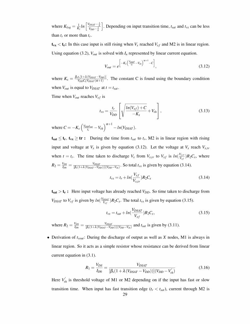
• Derivation of tvout : During the discharge of output as well as X nodes, M1 is always in
linear region. So it acts as a simple resistor whose resistance can be derived from linear
current equation in (3.1).
R1 =VDS
ID0=
VDSAT
[βs(1+λ (VDSAT −VDD))](VDD−V ′th)(3.16)
Here V′
th is threshold voltage of M1 or M2 depending on if the input has fast or slow
transition time. When input has fast transition edge (tr < tsat), current through M2 is29

large, current through M1 is limited by M1 itself and V′
th = Vth,M1. If input has slow
transition edge, current through M2 is small and current through M1 is limited by M2.
So V′
th =Vth. The time to discharge CL from VDD to VDD/2 is given by
tvout = 0.69R1CL. (3.17)
Case 2. Input given to top transistor: When input is given to top transistor, VX is already dis-
charged. So only Vout has to discharge from VDD to VDD/2 through the stack. This is equivalent
to an inverter where M1 and M2 are together and represented by a single transistor of almost
half the width. The delay is given by the equations (3.7) or (3.8) depending on whether the
input is fast or slow.
0 . 0 4 . 0 x 1 0 - 7 8 . 0 x 1 0 - 75 . 0 0 E - 0 1 2
1 . 0 0 E - 0 1 1
1 . 5 0 E - 0 1 1
2 . 0 0 E - 0 1 1
2 . 5 0 E - 0 1 1
3 . 0 0 E - 0 1 1 t p h l - a n a l y t i c a l t p h l - s i m u l a t e d
Delay
(s)
W i d t h ( m )0 . 0 4 . 0 x 1 0 - 1 5 8 . 0 x 1 0 - 1 5
t p h l - a n a l y t i c a l t p h l - s i m u l a t e d
L o a d C a p a c i t a n c e ( F )0 . 0 4 . 0 x 1 0 - 1 1 8 . 0 x 1 0 - 1 1
t p h l - a n a l y t i c a l t p h l - s i m u l a t e d
T r a n s i t i o n t i m e ( s )
Figure 3.10: NAND2 gate HL delay with varying width, capacitance, transition time when inputis given to M2 at 45nm technology node.
3.2.2 Model Validation
The plots in Figures 3.10 and 3.11 show the results using the proposed model and HSPICE
simulations for NAND2 gate when input is given to M2(bottom) and M1(top) respectively.
Delay values are plotted for varying widths, load capacitances and transition times. Similar to
inverter plots, fanin and fanout are kept constant at FO4 while sweeping width from 2 times
30

0 . 0 4 . 0 x 1 0 - 7 8 . 0 x 1 0 - 75 . 0 0 E - 0 1 2
1 . 0 0 E - 0 1 1
1 . 5 0 E - 0 1 1
2 . 0 0 E - 0 1 1
2 . 5 0 E - 0 1 1
3 . 0 0 E - 0 1 1 t p h l - a n a l y t i c a l t p h l - s i m u l a t e d
Delay
(s)
W i d t h ( m )0 . 0 4 . 0 x 1 0 - 1 5 8 . 0 x 1 0 - 1 5
t p h l - a n a l y t i c a l t p h l - s i m u l a t e d
L o a d C a p a c i t a n c e ( F )0 . 0 4 . 0 x 1 0 - 1 1 8 . 0 x 1 0 - 1 1
t p h l - a n a l y t i c a l t p h l - s i m u l a t e d
T r a n s i t i o n t i m e ( s )
Figure 3.11: NAND2 gate HL delay with varying width, capacitance, transition time when inputis given to M1 at 45nm technology node.
minimum width to 20 times minimum width. For varying load capacitance, fanout is swept
from FO4 to FO20, while fanin is kept at FO4 and width set at 4 times minimum length. For
varying input transition time, fanin is swept from FO4 to FO20, while fanout is fixed at FO10
and width is fixed at 4 times minimum width.
Similar to INV delay characteristics, delay in NAND2 gate is also almost invariant to
width, varies linearly with CL and varies linearly with tr for low transition times and saturates
for higher values. When input is given to M2 the average error when varying width is -0.16%,
when varying CL is -0.27% and when varying tr is 1.17%. When input is given to M1 the
average error when varying width is -2.92%, when varying CL is 1.02% and when varying tr is
-1.12%.
Similar plots are generated for NOR2 gate but for low to high delays. The average error
when input is given to M2(top) when varying width is -5.15%, when varying CL is -0.66% and
when varying tr is -0.31%. The average error when input is given to M1(bottom) when varying
width is -2.45%, when varying CL is -1.29% and when varying tr is 1.36%.
31

0 . 0 4 . 0 x 1 0 - 7 8 . 0 x 1 0 - 75 . 0 0 E - 0 1 2
1 . 0 0 E - 0 1 1
1 . 5 0 E - 0 1 1
2 . 0 0 E - 0 1 1
2 . 5 0 E - 0 1 1
3 . 0 0 E - 0 1 1 t p h l - a n a l y t i c a l t p h l - s i m u l a t e d
Delay
(s)
W i d t h ( m )0 . 0 4 . 0 x 1 0 - 1 5 8 . 0 x 1 0 - 1 5
t p h l - a n a l y t i c a l t p h l - s i m u l a t e d
L o a d C a p a c i t a n c e ( F )0 . 0 4 . 0 x 1 0 - 1 1 8 . 0 x 1 0 - 1 1
t p h l - a n a l y t i c a l t p h l - s i m u l a t e d
T r a n s i t i o n t i m e ( s )
Figure 3.12: NOR2 gate LH delay with varying width, capacitance, transition time when inputis given to bottom PMOS at 45nm technology node.
0 . 0 4 . 0 x 1 0 - 7 8 . 0 x 1 0 - 75 . 0 0 E - 0 1 2
1 . 0 0 E - 0 1 1
1 . 5 0 E - 0 1 1
2 . 0 0 E - 0 1 1
2 . 5 0 E - 0 1 1
3 . 0 0 E - 0 1 1 t p h l - a n a l y t i c a l t p h l - s i m u l a t e d
Delay
(s)
W i d t h ( m )0 . 0 4 . 0 x 1 0 - 1 5 8 . 0 x 1 0 - 1 5
t p h l - a n a l y t i c a l t p h l - s i m u l a t e d
L o a d C a p a c i t a n c e ( F )0 . 0 4 . 0 x 1 0 - 1 1 8 . 0 x 1 0 - 1 1
t p h l - a n a l y t i c a l t p h l - s i m u l a t e d
T r a n s i t i o n t i m e ( s )
Figure 3.13: NOR2 gate LH delay with varying width, capacitance, transition time when inputis given to top PMOS at 45nm technology node.
32

The low to high delays for NAND gates and high to low delays for NOR gates follow
the exact same equations for inverter because transistors are not stacked here and are equivalent
to inverters.
3.2.3 NAND3 Delay Model
M1
M2
A1
A2
M5A1 A2
X1
Out
X2
A3
A3
M3
M4 M6
CL
Figure 3.14: NAND3 gate schematics.
Delay equations for NAND3 are derived using a similar procedure. Figure 3.14 shows
a NAND3 gate where M1 is the top transistor, M2 is the middle transistor and M3 is the bottom
transistor.
Case 1. Input given to M1: This is the simplest case where nodes X1 and X2 are already
discharged and the voltage at the output node has to discharge through the three transistors. M1,
M2 and M3 are reduced to an equivalent transistor of almost one-third the width of NAND3
gate NMOS. The delay equation is similar to inverter delay given by equation (3.7) or (3.8)
depending on input slew rate.
Case 2. Input given to M2: In this case, X2 is already discharged but X1 and output node have
33

to be discharged. Delay depends on M2 and M1. It is given by sum of tvx1 and tvout .
Tphl = tvx1 + tvout −tr2
(3.18)
tvx1 is given by one of the equations (3.13), (3.14) and (3.15) depending on the input slew rate.
tvout is given by
tvout = 0.69R1CL. (3.19)
where R1 =VDSID0
= VDSAT[βs(1+λ (VDSAT−VDD))](VGS−Vth)
Case 3. Input given to M3: In this case both X1 and X2 are charged and delay depends on all
the three transistors M1, M2 and M3.
Tphl = tvx1 + tvx2 + tvout −tr2
(3.20)
tvx2 is given by one of the equations (3.13), (3.14) and (3.15) depending on the input slew rate.
tvx1 is similar to tvout because M2 is also in linear region all through the discharge of Vout . RC
constant is multiplied by 0.4 because there is only around 30% discharge. Thus tvx2 is given by
tvx2 = 0.4R2(CL +Cx1). (3.21)
where R2 =VDSID0
= VDSAT[βs(1+λ (VDSAT−VDD))](VGS2−Vth)
Finally tvout is given by
tvout = 0.69R1CL (3.22)
where R1 =VDSID0
= VDSAT[βs(1+λ (VDSAT−VDD))](VGS1−Vth)
3.2.4 NAND3 Validation
The plots for NAND3 gate when input is given to top, middle and bottom transistors are given
in Figures 3.15, 3.16 and 3.17, respectively. The average error when input is given to M1(top)
when varying width is -3.16%, when varying CL is 1.01%and when varying tr is 0.44%. The
average error when input is given to M2(middle) when varying width is -0.10%, when varying
CL is 2.69%and when varying tr is 0.58%. The average error when input is given to M3(bottom)
when varying width is 1.71%, when varying CL is 1.91% and when varying tr is 1.01%.
34

3.2.5 Summary:
In this chapter we derived nominal delay models for inverter and stacked transistors such as
NAND2, NOR2 and NAND3. Delay predicted is in good agreement with simulated results.
Hence this approach can be extended to any complex circuit considering input transition time,
load capacitance and stacking effect.
0 . 0 4 . 0 x 1 0 - 7 8 . 0 x 1 0 - 75 . 0 0 E - 0 1 2
1 . 0 0 E - 0 1 1
1 . 5 0 E - 0 1 1
2 . 0 0 E - 0 1 1
2 . 5 0 E - 0 1 1
3 . 0 0 E - 0 1 1 t p h l - a n a l y t i c a l t p h l - s i m u l a t e d
Delay
(s)
W i d t h ( m )0 . 0 4 . 0 x 1 0 - 1 5 8 . 0 x 1 0 - 1 5
t p h l - a n a l y t i c a l t p h l - s i m u l a t e d
L o a d C a p a c i t a n c e ( F )0 . 0 4 . 0 x 1 0 - 1 1 8 . 0 x 1 0 - 1 1
t p h l - a n a l y t i c a l t p h l - s i m u l a t e d
T r a n s i t i o n t i m e ( s )
Figure 3.15: NAND3 gate HL delay with varying width, capacitance, transition time when inputis given to M1 at 45nm technology node.
35

0 . 0 4 . 0 x 1 0 - 7 8 . 0 x 1 0 - 75 . 0 0 E - 0 1 2
1 . 0 0 E - 0 1 1
1 . 5 0 E - 0 1 1
2 . 0 0 E - 0 1 1
2 . 5 0 E - 0 1 1
3 . 0 0 E - 0 1 1
3 . 5 0 E - 0 1 1 t p h l - a n a l y t i c a l t p h l - s i m u l a t e d
Delay
(s)
W i d t h ( m )0 . 0 4 . 0 x 1 0 - 1 5 8 . 0 x 1 0 - 1 5
t p h l - a n a l y t i c a l t p h l - s i m u l a t e d
L o a d C a p a c i t a n c e ( F )0 . 0 4 . 0 x 1 0 - 1 1 8 . 0 x 1 0 - 1 1
t p h l - a n a l y t i c a l t p h l - s i m u l a t e d
T r a n s i t i o n t i m e ( s )
Figure 3.16: NAND3 gate HL delay with varying width, capacitance, transition time when inputis given to M2 at 45nm technology node.
0 . 0 4 . 0 x 1 0 - 7 8 . 0 x 1 0 - 75 . 0 0 E - 0 1 2
1 . 0 0 E - 0 1 1
1 . 5 0 E - 0 1 1
2 . 0 0 E - 0 1 1
2 . 5 0 E - 0 1 1
3 . 0 0 E - 0 1 1
3 . 5 0 E - 0 1 1 t p h l - a n a l y t i c a l t p h l - s i m u l a t e d
Delay
(s)
W i d t h ( m )0 . 0 4 . 0 x 1 0 - 1 5 8 . 0 x 1 0 - 1 5
t p h l - a n a l y t i c a l t p h l - s i m u l a t e d
L o a d C a p a c i t a n c e ( F )0 . 0 4 . 0 x 1 0 - 1 1 8 . 0 x 1 0 - 1 1
t p h l - a n a l y t i c a l t p h l - s i m u l a t e d
T r a n s i t i o n t i m e ( s )
Figure 3.17: NAND3 gate HL delay with varying width, capacitance, transition time when input
is given to M3 at 45nm technology node.
36

The parameters required in the model are given in Table 3.1. The parameters α , λ ,
Vth, ID0 and VDSAT are extracted from device characteristics. The parameters load capacitance
and final voltage, Vx f , that node X reaches are parameters from the circuit level. All other
parameters like Ky, Kz, K2, Klog C and Kx are derived from the parameters in Table 3.1.
Parameter ExtractionInformation
α 1 for technologies consideredλ Device characteristics
Vth Device characteristicsID0 Device characteristics
VDSAT Device characteristicsCL Circuit characteristicsVx f Circuit characteristics
Table 3.1: Parameters used in the model and their extraction information.
37
Chapter 4
ANALYTICAL MODEL FOR DELAY VARIABILITY
This chapter analyzes variation in delay due to variations in threshold voltage. The delay equa-
tions derived in Chapter 3 are used to predict delay variability. Delay variability of inverter is
derived in Section 4.1. In Section 4.2 variability model is extended to NAND2 and NOR2
gates and later to NAND3 gates in Section 4.3. This model is validated with PTM models [4]
at 45nm technology and 32nm technology nodes.
4.1 Delay Variability in Inverter
Threshold voltage variation in transistors is assumed to follow Gaussian distribution. So delay
variation should also follow Gaussian distribution with standard deviation, σTp [28].
σTp =∂ (Tphl)
∂VthσVth (4.1)
Equation (4.1) can be applied on the delay equation of any gate to get delay variability due to
Vth variation. For an inverter with slow rising input or small load capacitance, inverter delay
follows equation (3.7) and variability in such case is given by
σTp =tr
VDDσVth . (4.2)
For an inverter with fast rising inputs or large load capacitance, inverter delay follows
equation (3.8) and variability in such case is given by
σTp = [S1+S2(S3−S4)]σVth , (4.3)
where S1= 1Kz(VDD−Vth)
ln[
0.5VDD−K2VDD− 1
λ
], S2= 1
Kz
[VDD− 1
λ
0.5VDD−K2
], S3=
(eKy(Vin−Vth)
α+1)(α+1)Ky(VDD−
Vth)α and S4 = eKztr λβstr
CL. Here α is velocity saturation index and is taken to be α = 1 for
technologies considered, λ is the empirical channel length modulation factor, βs =ID0
(VDD−Vth)α ,
Ky =βstrλ
CL(α+1)VDD, Kz =
βsλ (VDD−Vth)α
CL, K2 =
(VDD− 1
λ
)((eKy(VDD−Vth)
α+1)− eKztr
)+ 1
λ.
Delay variability obtained analytically is compared with HSPICE Monte Carlo simu-
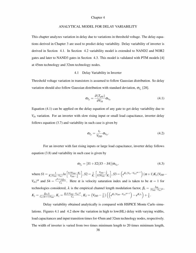
lations. Figures 4.1 and 4.2 show the variation in high to low(HL) delay with varying widths,
load capacitances and input transition times for 45nm and 32nm technology nodes, respectively.
The width of inverter is varied from two times minimum length to 20 times minimum length,38

keeping fanin and fanout constant at FO4. To study the effect of load capacitance, fanin and
width are kept constant while varying load capacitance. To study the effect of input slew rate,
fanout and width are constant while varying input transition times. Here the baseline voltage
variation is 50mV corresponding to twice minimum width and the threshold voltage varies with
width as σVth ∝1√W
, where W is width of the transistor.
0 . 0 4 . 0 x 1 0 - 7 8 . 0 x 1 0 - 70 . 0
2 . 0 x 1 0 - 1 3
4 . 0 x 1 0 - 1 3
6 . 0 x 1 0 - 1 3
8 . 0 x 1 0 - 1 3
1 . 0 x 1 0 - 1 2
1 . 2 x 1 0 - 1 2
1 . 4 x 1 0 - 1 2
( a )
s i g m a - a n a l y t i c a l s i g m a - s i m u l a t e d
Delay
Varia
tion S
igma(s
)
W i d t h ( m )0 . 0 4 . 0 x 1 0 - 1 5 8 . 0 x 1 0 - 1 5
( b )
s i g m a - a n a l y t i c a l s i g m a - s i m u l a t e d
L o a d C a p a c i t a n c e ( F )0 . 0 4 . 0 x 1 0 - 1 1 8 . 0 x 1 0 - 1 1
( c )
s i g m a - a n a l y t i c a l s i g m a - s i m u l a t e d
T r a n s i t i o n t i m e ( s )
Figure 4.1: Inverter HL delay variation with varying (a) width, (b) capacitance, (c) transitiontime at 45nm technology node.
Our observations are as follows.
• Since varying width does not have any effect on nominal delay (see Figure 3.4), σTp varies
in proportion to σVth , as shown in Figures 4.1a and 4.2a.
• Increasing load capacitance makes equation (4.3) applicable. According to this equation,
S1 and S2 are proportional to 1Kz
, where Kz is proportional to 1CL
. S3 and S4 vary almost
similarly canceling out each others effect. So σTp varies linearly with CL, as shown in
Figures 4.1b and 4.2b.
• Increasing input transition time is modeled by equation (4.2), according to which σTp is
proportional to tr. The trend is also very clearly seen in Figures 4.1c and 4.2c.
39
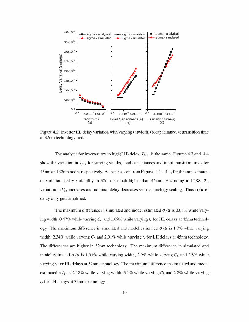
0 . 0 4 . 0 x 1 0 - 7 8 . 0 x 1 0 - 70 . 0
5 . 0 x 1 0 - 1 3
1 . 0 x 1 0 - 1 2
1 . 5 x 1 0 - 1 2
2 . 0 x 1 0 - 1 2
2 . 5 x 1 0 - 1 2
3 . 0 x 1 0 - 1 2
3 . 5 x 1 0 - 1 2
4 . 0 x 1 0 - 1 2 s i g m a - a n a l y t i c a l s i g m a - s i m u l a t e d
Delay
Varia
tion S
igma(s
)
W i d t h ( m )0 . 0 4 . 0 x 1 0 - 1 5 8 . 0 x 1 0 - 1 5
s i g m a - a n a l y t i c a l s i g m a - s i m u l a t e d
L o a d C a p a c i t a n c e ( F )( a ) ( b ) ( c )
0 . 0 4 . 0 x 1 0 - 1 1 8 . 0 x 1 0 - 1 1
s i g m a - a n a l y t i c a l s i g m a - s i m u l a t e d
T r a n s i t i o n t i m e ( s )
Figure 4.2: Inverter HL delay variation with varying (a)width, (b)capacitance, (c)transition timeat 32nm technology node.
The analysis for inverter low to high(LH) delay, Tplh, is the same. Figures 4.3 and 4.4
show the variation in Tplh for varying widths, load capacitances and input transition times for
45nm and 32nm nodes respectively. As can be seen from Figures 4.1 - 4.4, for the same amount
of variation, delay variability in 32nm is much higher than 45nm. According to ITRS [2],
variation in Vth increases and nominal delay decreases with technology scaling. Thus σ/µ of
delay only gets amplified.
The maximum difference in simulated and model estimated σ/µ is 0.68% while vary-
ing width, 0.47% while varying CL and 1.09% while varying tr for HL delays at 45nm technol-
ogy. The maximum difference in simulated and model estimated σ/µ is 1.7% while varying
width, 2.34% while varying CL and 2.01% while varying tr for LH delays at 45nm technology.
The differences are higher in 32nm technology. The maximum difference in simulated and
model estimated σ/µ is 1.93% while varying width, 2.9% while varying CL and 2.8% while
varying tr for HL delays at 32nm technology. The maximum difference in simulated and model
estimated σ/µ is 2.18% while varying width, 3.1% while varying CL and 2.8% while varying
tr for LH delays at 32nm technology.
40

0 . 0 4 . 0 x 1 0 - 7 8 . 0 x 1 0 - 7
5 . 0 x 1 0 - 1 3
1 . 0 x 1 0 - 1 2
1 . 5 x 1 0 - 1 2
2 . 0 x 1 0 - 1 2
2 . 5 x 1 0 - 1 2
3 . 0 x 1 0 - 1 2 s i g m a - s i m u l a t e d s i g m a - a n a l y t i c a l
Delay
Varia
tion S
igma(s
)
W i d t h ( m )0 . 0 4 . 0 x 1 0 - 1 5 8 . 0 x 1 0 - 1 5
s i g m a - s i m u l a t e d s i g m a - a n a l y t i c a l
L o a d C a p a c i t a n c e ( F )0 . 0 4 . 0 x 1 0 - 1 1 8 . 0 x 1 0 - 1 1
s i g m a - s i m u l a t e d s i g m a - a n a l y t i c a l
T r a n s i t i o n t i m e ( s )
Figure 4.3: Inverter LH delay variation with varying width, capacitance, transition time at 45nm
technology node.
0 . 0 4 . 0 x 1 0 - 7 8 . 0 x 1 0 - 7
5 . 0 x 1 0 - 1 3
1 . 0 x 1 0 - 1 2
1 . 5 x 1 0 - 1 2
2 . 0 x 1 0 - 1 2
2 . 5 x 1 0 - 1 2
3 . 0 x 1 0 - 1 2
3 . 5 x 1 0 - 1 2 s i g m a - a n a l y t i c a l s i g m a - s i m u l a t e d
Delay
Varia
tion S
igma(s
)
W i d t h ( m )0 . 0 4 . 0 x 1 0 - 1 5 8 . 0 x 1 0 - 1 5
s i g m a - a n a l y t i c a l s i g m a - s i m u l a t e d
L o a d C a p a c i t a n c e ( F )0 . 0 4 . 0 x 1 0 - 1 1 8 . 0 x 1 0 - 1 1
s i g m a - a n a l y t i c a l s i g m a - s i m u l a t e d
T r a n s i t i o n t i m e ( s )
Figure 4.4: Inverter LH delay variation with varying width, capacitance, transition time at 32nm
technology node.
41
4.2 Delay Variability in NAND2 and NOR2 gates
Delay variations in NAND and NOR gates can also be derived using equation (4.1). Delay
variation for NAND2 high to low delay is given below. The variation depends on whether input
is given to top transistor or bottom transistor of the stack.
Case 1. Input given to bottom transistor: When input is given to bottom transistor (M2 of
Figure 3.8), Vth variation in any of the transistors in the stack affects delay variation.
1. Variation in Vth of bottom transistor: Partial derivative of NAND2 delay equation (3.10)
with respect to Vth gives three solutions according to the input slew rate. tsat is time
taken for the intermediate node voltage Vx to discharge from initial value of VDD−Vth,M1
to VDSAT and is given in equation (3.11). tvx is the time taken for Vx to discharge from
initial value of VDD−Vth,M1 to Vx f , where Vx f is the final voltage at node X when Vout is
discharged to VDD/2. It is given in equations (3.13), (3.14) and (3.15).
tvx < tr : For this case, input is very slow and Vx reaches its final value before input
reaches VDD. The variation in delay is given as:
σTp =
(tr
VDD+
0.69R1CL
VDD−Vth
)σVth . (4.4)
tsat < tr, tvx > tr : For this case, input is slow and Vx reaches VDSAT before input reaches
VDD, but Vx reaches its final value after input reaches VDD. The variation in delay is given
as:
σTp =
(2Kx(VDD−Vth)R1(CL +Cx)+
ln(Vx,tr/Vx f )R1(CL +Cx)
(VDD−Vth)
)σVth . (4.5)
where Kx =βstr[1+λ (VDSAT−VDD)]
VDDCLVDSAT (α+1) .
tvx > tr : For this case, input is fast and input reaches VDD before even Vx reaches VDSAT .
The variation in delay is given as:
σTp =
(tr
VDD+
ln(VDSAT/Vx f )R1CL
VDD−Vth
)σVth . (4.6)
2. Variation in Vth of top transistor: The partial derivative of equation (3.10) with respect to
Vth,M1 gives three possible solutions depending on the input transition time.
42

tvx < tr : For this case, input is very slow and Vx reaches its final value before input
reaches VDD. The variation in delay is given as:
σTp =
tr
VDDKy
√ln(Vx f )+C−Kx
(VDD−1/λ +Vth,M1)
σVth . (4.7)
where Kx =βstr[1+λ (VDSAT−VDD)]
VDDCLVDSAT (α+1) , Ky =βstrλ
CL(α+1)VDD, C =−Kx
(VDDtsat
tr−Vth
)α+1− ln(VDSAT ).
tsat < tr, tvx > tr : For this case, input is slow and Vx reaches VDSAT before input reaches
VDD, but reaches its final value after input reached VDD. The variation in delay is given
as:
σTp =
(R1CLKx
Ky ∗ (VDD−1/λ +Vth,M1)
)σVth . (4.8)
tvx > tr : For this case, input is fast and input reaches VDD before even Vx reaches VDSAT .
The variation in delay is given as:
σTp =
(tr
VDD ∗√
KlogKy(VDD−1/λ +Vth,M1)+
0.69R1CL
VDD−Vth,M1
)σVth . (4.9)
where where Klog =1
Kyln[
0.5VDD− 1λ
VDD− 1λ
].
Case 2. Input given to top transistor: When input is given to top transistor, delay depends
only on Vth of top transistor. So variation in delay is given by inverter delay variation as in equa-
tions (4.2) or (4.3) depending on the region or operation when Vout reaches VDD/2. So variation
in bottom transistor should have almost no effect on the delay in this case.
Model Validation: Table 4.1 shows variation when input is given to top(M1) and bottom(M2)
transistors. In each case Vth of only M1 or M2 is varied. NAND2 gate is loaded with FO10 and
fanin is set at FO4. Width of gate is taken to be 4 times minimum size, that is width of PMOS
transistors is 4 times minimum size and width of NMOS transistors is 8 times the minimum
width. Amount of Vth variation added is calculated using the method in [32]. Simulated and
model estimated results show that, when input is given to M1, delay variability depends only on
Vth of M1 alone. But when input is given to M2, Vth of both M1 and M2 affect delay variability.
Simulation results closely match with model estimated values.
43

Input transistor Variation transistor Simulated Analytical
µ (ps) σ (ps) σ/µ % µ (ps) σ (ps) σ/µ %
M1M1 15.60 1.68 10.77 13.86 1.17 8.43
M2 15.50 0.34 2.19 13.86 ˜0 ˜0
M2M1 16.50 0.91 5.52 16.14 0.97 6.01
M2 16.50 1.49 9.03 16.14 1.52 9.42
Table 4.1: Variation numbers when input is given to top(M1) and bottom(M2) transistors of
NAND2 gate, with Vth of one of them varying.
NAND2 HL delay variations when input is given to top and bottom transistors are plot-
ted for 45nm technology in Figures 4.5 and 4.6. Figures show NAND2 delay variations with
varying widths, load capacitances and transition times. The maximum difference in predicted
and HSPICE simulated σ/µ is 1.7% when varying width, 1.4% when varying load capaci-
tance and 1.7% when varying input transition time when input is given to top(M1) transistor.
When input is given to bottom(M2) transistor, maximum difference between model estimated
and HSPICE simulated σ/µ is 1.3% while varying width, 0.90% while varying load capaci-
tance and 0.69% while varying input transition time. Thus in all cases the difference between
estimated results and HSPICE simulation results is very small.
4.3 Delay Variability in NAND3
Similar analysis is used to derive equations for delay variability of NAND3. Delay variation
depends on whether the input is given to the bottom, middle or top transistor.
Case 1. Input given to bottom transistor: When input is given to bottom transistor, Vth
variation in top most transistor and bottom most transistor affects delay variability. Middle
transistor variation by itself does not have significant effect on delay variability because its
variation is compensated either by top or bottom transistors.
1. Variation in Vth of bottom transistor: Partial derivative of equation (3.20) with respect to
Vth gives equations (4.6) , (4.5) and (4.4) according to input transition time.
2. Variation in Vth of top transistor: Partial derivative of equation (3.20) with respect to
44

0 . 0 4 . 0 x 1 0 - 7 8 . 0 x 1 0 - 70 . 0
5 . 0 x 1 0 - 1 3
1 . 0 x 1 0 - 1 2
1 . 5 x 1 0 - 1 2
2 . 0 x 1 0 - 1 2
2 . 5 x 1 0 - 1 2
3 . 0 x 1 0 - 1 2 s i g m a - a n a l y t i c a l s i g m a - s i m u l a t e d
Delay
Varia
tion S
igma(s
)
W i d t h ( m )0 . 0 4 . 0 x 1 0 - 1 5 8 . 0 x 1 0 - 1 5
s i g m a - a n a l y t i c a l s i g m a - s i m u l a t e d
L o a d C a p a c i t a n c e ( F )0 . 0 4 . 0 x 1 0 - 1 1 8 . 0 x 1 0 - 1 1
s i g m a - a n a l y t i c a l s i g m a - s i m u l a t e d
T r a n s i t i o n t i m e ( s )
Figure 4.5: NAND2 gate HL delay variation with varying width, capacitance, transition timewhen input is given to M2 at 45nm technology node.
0 . 0 4 . 0 x 1 0 - 7 8 . 0 x 1 0 - 70 . 0
5 . 0 x 1 0 - 1 3
1 . 0 x 1 0 - 1 2
1 . 5 x 1 0 - 1 2
2 . 0 x 1 0 - 1 2
2 . 5 x 1 0 - 1 2 s i g m a - a n a l y t i c a l s i g m a - s i m u l a t e d
Delay
Varia
tion S
igma(s
)
W i d t h ( m )0 . 0 4 . 0 x 1 0 - 1 5 8 . 0 x 1 0 - 1 5
s i g m a - a n a l y t i c a l s i g m a - s i m u l a t e d
L o a d C a p a c i t a n c e ( F )0 . 0 4 . 0 x 1 0 - 1 1 8 . 0 x 1 0 - 1 1
s i g m a - a n a l y t i c a l s i g m a - s i m u l a t e d
T r a n s i t i o n t i m e ( s )
Figure 4.6: NAND2 gate HL delay variation with varying width, capacitance, transition timewhen input is given to M1 at 45nm technology node.
45

Vth,M1 for the case when tsat > tr gives
σTp =
(tr
VDD ∗√
KlogKy(VDD−1/λ +Vth,M1)+
0.69R1(CL +Cx)
VDD−Vth,M1+
0.4R2CL
VDD−Vth,M1
)σVth .
(4.10)
For the other two cases when tsat < tr and tvx < tr, equations (4.5) and (4.4) hold true.
Case 2. Input given to middle transistor: When input is given to middle transistor, Vth varia-
tion in any of the top or middle transistors affects delay variation. Bottom most transistor does
not affect output delay hence does not affect variability.
1. Variation in Vth of middle transistor: Partial derivative of equation (3.20) with respect to
Vth gives equations similar to (4.4), (4.5) and (4.6) depending on input slew rate.
2. Variation in Vth of top transistor: Partial derivative of equation (3.20) with respect to
Vth,M1 gives equations similar to (4.7), (4.8) and (4.9) according to input transition time.
Case 3. Input given to top transistor: When input is given to top transistor, delay depends
only on Vth of top transistor. So variation in delay is given by inverter delay variation equation
as in (4.2) or (4.3) depending on the region when Vout reaches VDD/2. So variation in middle or
bottom transistor should have almost no effect on the delay variation.
Model Validation: Table 4.2 shows variation when input is given to top(M1), middle(M2) and
bottom(M3) transistors. In each case Vth of only M1, M2 or M3 transistor is varied. NAND3
gate considered is 4 times minimum length, that is PMOS transistor is 4 times minimum length
and NMOS is 12 times minimum length. It is loaded with FO10 and fanin is FO4. Amount
of Vth variation to be added is calculated using method from [32]. As expected, when input
is given to M3 transistor, Vth variation in M1 and M3 results in considerable delay variability
but variation in M2 transistor has almost no effect. When input is given to M2 transistor, it is
similar to NAND2 gate. So variation in M1 and M2 transistors add to variability, but bottom
transistor does not have any effect. When input is given to M1 transistor, variation in only M1
affects delay. Simulation results match very well with model estimated values.
46

Input transistor Variation transistor Simulated Analyticalµ (ps) σ (ps) σ/µ % µ (ps) σ (ps) σ/µ %
M1M1 15.29 0.63 4.14 15.29 0.51 3.34M2 15.22 0.16 1.06 15.29 ˜0 ˜0M3 15.19 0.14 0.94 15.29 ˜0 ˜0
M2M1 17.66 0.32 1.83 16.57 0.64 3.86M2 17.68 0.58 3.26 16.57 0.64 3.86M3 17.62 0.11 0.62 16.57 ˜0 ˜0
M3M1 18.02 0.34 1.90 18.47 0.64 3.47M2 18.00 0.21 1.16 18.47 ˜0 ˜0M3 18.06 0.63 3.47 18.47 0.64 3.47
Table 4.2: Variation numbers when input is given to top(M1), middle(M2) and bottom(M3)transistors of NAND3 gate, with Vth of one of them varying.
NAND3 delay variations at 45nm are plotted in Figures 4.7, 4.8 and 4.9 when input
is given to M1, M2 and M3 transistors, respectively. Figures show delay variations for varying
widths, load capacitances and input transition times. The maximum difference in predicted and
HSPICE simulated σ/µ is 0.75% while varying width, 0.97% while varying load capacitance
and 0.82% while varying input slew rate when input is given to M1. The maximum difference in
predicted and HSPICE simulated σ/µ is 0.42% while varying width, 0.63% while varying load
capacitance and 0.63% while varying input slew rate when input is given to M2. The maximum
difference in predicted and HSPICE simulated σ/µ is 0.15% while varying width, 0.48% while
varying load capacitance and 0.6% while varying input slew rate when input is given to M3.
Interestingly for large load capacitances, delay variability is high when input is given
to M1 transistor than when given to M2 and M3 transistors for NAND3. Similar is the trend for
NAND2. This is because, discharge rate of M1, M2 and M3 affect delay when input is given
to M3 and discharge rate of M1 and M2 affect delay when input is given to M2. But when
input is given to M1, output depends on discharge rate of only M1. When load is high, the
current reaches maximum value in M1 increasing nominal delay to a large extent. As variability
depends on nominal delay also, large loads result in high delay variability.
47

0 . 0 4 . 0 x 1 0 - 7 8 . 0 x 1 0 - 70 . 0
5 . 0 x 1 0 - 1 3
1 . 0 x 1 0 - 1 2
1 . 5 x 1 0 - 1 2
2 . 0 x 1 0 - 1 2
2 . 5 x 1 0 - 1 2 s i g m a - a n a l y t i c a l s i g m a - s i m u l a t e d
Delay
Varia
tion S
igma(s
)
W i d t h ( m )0 . 0 4 . 0 x 1 0 - 1 5 8 . 0 x 1 0 - 1 5
s i g m a - a n a l y t i c a l s i g m a - s i m u l a t e d
L o a d C a p a c i t a n c e ( F )0 . 0 4 . 0 x 1 0 - 1 1 8 . 0 x 1 0 - 1 1
s i g m a - a n a l y t i c a l s i g m a - s i m u l a t e d
T r a n s i t i o n t i m e ( s )
Figure 4.7: NAND3 gate HL delay variation with varying width, capacitance, transition time
when input is given to M1 at 45nm technology node.
0 . 0 4 . 0 x 1 0 - 7 8 . 0 x 1 0 - 70 . 0
5 . 0 x 1 0 - 1 3
1 . 0 x 1 0 - 1 2
1 . 5 x 1 0 - 1 2
2 . 0 x 1 0 - 1 2
2 . 5 x 1 0 - 1 2 s i g m a - a n a l y t i c a l s i g m a - s i m u l a t e d
Delay
Varia
tion S
igma(s
)
W i d t h ( m )0 . 0 4 . 0 x 1 0 - 1 5 8 . 0 x 1 0 - 1 5
s i g m a - a n a l y t i c a l s i g m a - s i m u l a t e d
L o a d C a p a c i t a n c e ( F )0 . 0 4 . 0 x 1 0 - 1 1 8 . 0 x 1 0 - 1 1
s i g m a - a n a l y t i c a l s i g m a - s i m u l a t e d
T r a n s i t i o n t i m e ( s )
Figure 4.8: NAND3 gate HL delay variation with varying width, capacitance, transition time
when input is given to M2 at 45nm technology node.
48
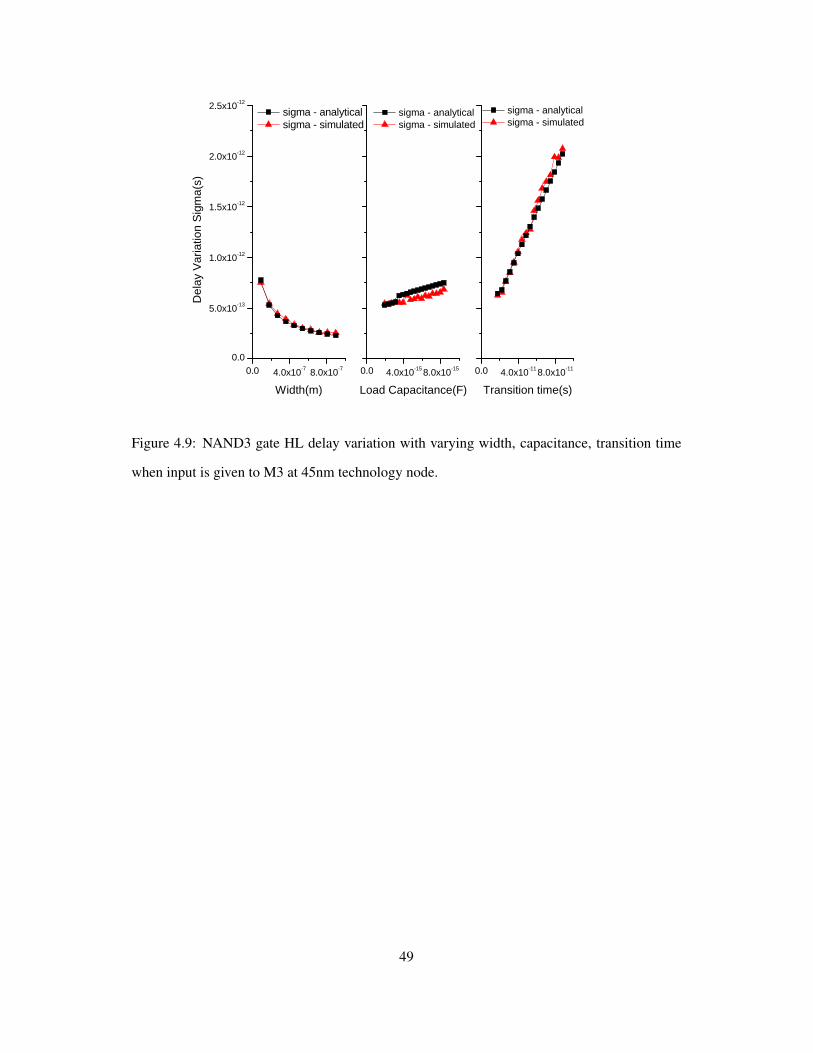
0 . 0 4 . 0 x 1 0 - 7 8 . 0 x 1 0 - 70 . 0
5 . 0 x 1 0 - 1 3
1 . 0 x 1 0 - 1 2
1 . 5 x 1 0 - 1 2
2 . 0 x 1 0 - 1 2
2 . 5 x 1 0 - 1 2 s i g m a - a n a l y t i c a l s i g m a - s i m u l a t e d
Delay
Varia
tion S
igma(s
)
W i d t h ( m )0 . 0 4 . 0 x 1 0 - 1 5 8 . 0 x 1 0 - 1 5
s i g m a - a n a l y t i c a l s i g m a - s i m u l a t e d
L o a d C a p a c i t a n c e ( F )0 . 0 4 . 0 x 1 0 - 1 1 8 . 0 x 1 0 - 1 1
s i g m a - a n a l y t i c a l s i g m a - s i m u l a t e d
T r a n s i t i o n t i m e ( s )
Figure 4.9: NAND3 gate HL delay variation with varying width, capacitance, transition time
when input is given to M3 at 45nm technology node.
49
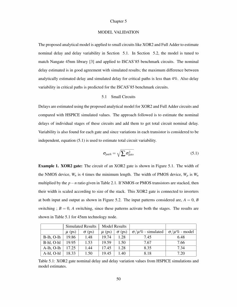
Chapter 5
MODEL VALIDATION
The proposed analytical model is applied to small circuits like XOR2 and Full Adder to estimate
nominal delay and delay variability in Section 5.1. In Section 5.2, the model is tuned to
match Nangate 45nm library [3] and applied to ISCAS’85 benchmark circuits. The nominal
delay estimated is in good agreement with simulated results; the maximum difference between
analytically estimated delay and simulated delay for critical paths is less than 4%. Also delay
variability in critical paths is predicted for the ISCAS’85 benchmark circuits.
5.1 Small Circuits
Delays are estimated using the proposed analytical model for XOR2 and Full Adder circuits and
compared with HSPICE simulated values. The approach followed is to estimate the nominal
delays of individual stages of these circuits and add them to get total circuit nominal delay.
Variability is also found for each gate and since variations in each transistor is considered to be
independent, equation (5.1) is used to estimate total circuit variability.
σpath =√
∑σ2gate (5.1)
Example 1. XOR2 gate: The circuit of an XOR2 gate is shown in Figure 5.1. The width of
the NMOS device, Wn is 4 times the minimum length. The width of PMOS device, Wp is Wn
multiplied by the p−n ratio given in Table 2.1. If NMOS or PMOS transistors are stacked, then
their width is scaled according to size of the stack. This XOR2 gate is connected to inverters
at both input and output as shown in Figure 5.2. The input patterns considered are, A = 0, B
switching ; B = 0, A switching, since these patterns activate both the stages. The results are
shown in Table 5.1 for 45nm technology node.
Simulated Results Model Resultsµ (ps) σ (ps) µ (ps) σ (ps) σ/µ% - simulated σ/µ% - model
B-lh, O-lh 19.86 1.48 19.74 1.28 7.45 6.48B-hl, O-hl 19.95 1.53 19.59 1.50 7.67 7.66A-lh, O-lh 17.25 1.44 17.45 1.28 8.35 7.34A-hl, O-hl 18.33 1.50 19.45 1.40 8.18 7.20
Table 5.1: XOR2 gate nominal delay and delay variation values from HSPICE simulations andmodel estimates.
50

Figure 5.1: Schematic of XOR2 circuit
NOTNOTXOR
NOT
NOT3X 3X
Figure 5.2: XOR2 gate with input and output loading with FO4.
Table 5.1 shows the that maximum error between simulated and estimated σ/µ is less
than 1%. Such an accurate prediction of nominal delay and delay variation has been possible
because the model considers load capacitance, transition times and stacking effect.
Example 2. Full Adder: The full adder circuit is shown in Figure 5.3. The transistor widths
considered are similar to XOR2 gate, namely, Wn is 4 times minimum length and Wp is Wn
multiplied by the p− n ratio from Table 2.1. If NMOS or PMOS transistors are stacked, then
their width is scaled according to number of transistors stacked. This full adder is connected to
inverter at both input and output as shown in Figure 5.4.
The input patterns considered are, A = 1, Ci = 0, B switching ; B = 0, Ci = 1, A switch-
ing since these patterns activate both the stages. The results are shown in Table 5.2. The
maximum difference between the σ/µ estimates and simulated value is 0.65%.
51

A
A
A
A
BB
BB
Ci
A CiB
A B Ci A
A
B
B
Ci
CiCo' So'
Figure 5.3: Mirror Adder structure of Full Adder
NOT NOT
NOT
NOT3X 3X
NANDFA
Figure 5.4: Full Adder with input and output loading with FO4.
Simulated Results Model Resultsµ (ps) σ (ps) µ (ps) σ (ps) σ/µ% - simulated σ/µ% - model
B-lh, O-lh 24.73 1.726 22.63 1.611 6.98 7.12B-hl, O-hl 21.96 1.456 22.84 1.647 6.63 7.21A-lh, O-lh 24.96 1.868 23.65 1.681 7.48 7.11A-hl, O-hl 26.36 1.712 26.36 1.882 6.49 7.14
Table 5.2: Full Adder nominal delay and delay variation values from simulated results andmodel estimated results.
5.2 Application to ISCAS Benchmark Circuits
Setup: The proposed model has been tuned to match the Nangate 45nm technology library [3].
The model is verified for gates with drive strength X1 in the library. Here input transition times
range from 7.5ps to 600ps and load capacitance ranges from 0.4fF to 25.6fF. 10 ISCAS bench-
52
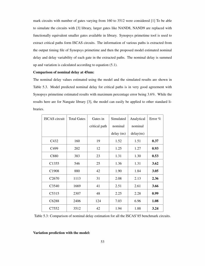
mark circuits with number of gates varying from 160 to 3512 were considered [1] To be able
to simulate the circuits with [3] library, larger gates like NAND8, NAND9 are replaced with
functionally equivalent smaller gates available in library. Synopsys primetime tool is used to
extract critical paths form ISCAS circuits. The information of various paths is extracted from
the output timing file of Synopsys primetime and then the proposed model estimated nominal
delay and delay variability of each gate in the extracted paths. The nominal delay is summed
up and variation is calculated according to equation (5.1).
Comparison of nominal delay at 45nm:
The nominal delay values estimated using the model and the simulated results are shown in
Table 5.3. Model predicted nominal delay for critical paths is in very good agreement with
Synopsys primetime estimated results with maximum percentage error being 3.6%. While the
results here are for Nangate library [3], the model can easily be applied to other standard li-
braries.
ISCAS circuit Total Gates Gates in Simulated Analytical Error %
critical path nominal nominal
delay (ns) delay(ns)
C432 160 19 1.52 1.51 0.37
C499 202 12 1.25 1.27 0.93
C880 383 23 1.31 1.30 0.53
C1355 546 25 1.36 1.31 3.62
C1908 880 42 1.90 1.84 3.05
C2670 1113 31 2.08 2.13 2.36
C3540 1669 41 2.51 2.61 3.66
C5315 2307 48 2.25 2.28 0.99
C6288 2406 124 7.03 6.96 1.08
C7552 3512 42 1.94 1.88 3.24
Table 5.3: Comparison of nominal delay estimation for all the ISCAS’85 benchmark circuits.
Variation prediction with the model:
53

The delay variability of critical paths of the ISCAS benchmark circuits is estimated. Amount of
Vth variation added is 50mV for a transistor of twice the minimum length and σVth ∝1√W
, where
W is the width of transistor. Table 5.4 shows delay variation for all the ISCAS benchmark
circuits. The average variation is 1.7%. The time taken to estimate variability with the model is
a very small fraction of the time taken to run SPICE simulations.
ISCAS circuit Nominal Delay(ps) Variation (ps) σ/µ %
C432 1512.70 37.56 2.48
C499 1244.10 33.88 2.68
C880 1293.00 26.16 2.01
C1355 1321.70 27.11 2.07
C1908 1840.10 32.87 1.78
C2670 2141.90 27.13 1.27
C3540 2600.80 37.97 1.46
C5315 2261.50 27.33 1.20
C6288 6776.90 48.59 0.70
C7552 1875.10 24.18 1.34
Table 5.4: Variation prediction for critical paths in ISCAS’85 benchmark circuits
The variation is small in these circuits because of averaging out of random variations
in these long paths.
5.2.1 Effects of Variability
The proposed analytical model is used to identify possible timing violations early in the design
flow.
Setup time violations: Setup time violations are caused by variations in critical paths. Vari-
ability is low in these paths because of averaging effect. However, paths with slightly smaller
delay can have larger variability and can become critical. Figure 5.5 shows the delay distribu-
tion graph for C880 benchmark circuit at nominal conditions and with Vth variations. As it can
be seen from the graph the distribution widens because of variations and the number of critical
paths increase. Some of the non-critical paths at nominal conditions have now become critical.54

The number of shortest paths also increase. The minimum delay decreased and this can cause a
hold violation.
0 2 0 0 4 0 0 6 0 0 8 0 0 1 0 0 0 1 2 0 0 1 4 0 0 1 6 0 00 . 0 0
0 . 0 5
0 . 1 0
0 . 1 5
0 . 2 0
0 . 2 5
0 . 3 0
I n c r e a s e d n u m b e r o f s h o r t p a t h s
Norm
alised
numb
er of
paths
D e l a y ( p s )
N o m i n a l W i t h V a r i a t i o n
I n c r e a s e d n u m b e r o f c r i t i c a l p a t h s
Figure 5.5: Delay distribution curve for C880 benchmark circuit at nominal and with variations.
Similar trend is seen in another circuit ISCAS C7552. Here the critical path has a nom-
inal delay of 1885.4ps and paths with 5% less than critical path delay are also considered as
critical paths. Consider Path-2 with a delay of 1787.3ps, that is 5.2% smaller than the critical
path and so not considered to be critical. Now with a slight Vth variation of σVth =10mV (for a
transistor with width twice the minimum length and σVth varying with the relation σVth ∝1√Wn
),
the worst case delay (µ +3σ ) of the critical path is 1900.5ps and of Path-2 is 1806.8ps, which
is within 5% of the critical path delay. Hence Path-2 now is also critical. Similarly, Path-3 with
nominal delay of 1777.7ps becomes critical for σVth=30mV. Figure 5.6 plots the worst case de-
lays of these paths as a function of σVth . The plot also shows that as σVth increases, the number
of critical paths increases. The proposed model can thus help easily identify paths that may
become critical due to Vth variations, early in the design phase and without time consuming
Monte Carlo simulations.
55

0 . 0 0 0 . 0 4 0 . 0 8 0 . 1 2 0 . 1 61 . 8 x 1 0 - 9
1 . 9 x 1 0 - 9
2 . 0 x 1 0 - 9
2 . 1 x 1 0 - 9
C r i t i c a l p a t h P a t h 3
Worst
Case
Delay
(s)
σ V t h
0 . 0 0 0 . 0 4 0 . 0 8 0 . 1 2 0 . 1 61 . 8 x 1 0 - 9
1 . 9 x 1 0 - 9
2 . 0 x 1 0 - 9
2 . 1 x 1 0 - 9
l e s s t h a n 5 % d i f f e r e n c e
C r i t i c a l p a t h P a t h 2
Worst
Case
Delay
(s)l e s s t h a n 5 % d i f f e r e n c e
Figure 5.6: Non-critical path becoming critical in light of Vth variation.
Hold time violations: The delay variability is small in long paths because of averaging effect.
But in smaller paths of the circuit, variation is considerable and the contaminated delays (µ −
3σ ) can cause hold time violations.
The proposed model is applied to two ISCAS benchmark circuits, C5315 and C2670,
to estimate the nominal delay and delay variability of the shortest paths. Hold time is assumed
to be 15ps for D-Flip Flop from [3] for reasonable data and clock transition times. There are no
hold violations under nominal conditions. But as variation in Vth increases, contaminated delays
of many paths fall below hold time. Figure 5.7 shows the number of possible hold violations
with varying σVth . For instance, when σVth=50mV, there are 12 hold violations in C5315 and 8
hold violations in C2670.
To avoid the hold time violations, design can be quickly modified by adding buffers to
the identified shortest paths and the new design is verified for timing violations by the proposed
model. For one of the failing paths in the C5315 ISCAS benchmark circuit, the nominal delay
is 19.2ps and path length is 1 gate. With σVth of 50mV, delay variation is 1.58ps, causing a hold
violation. But with the addition of a buffer(two inverters), nominal delay is now 63.1ps and56
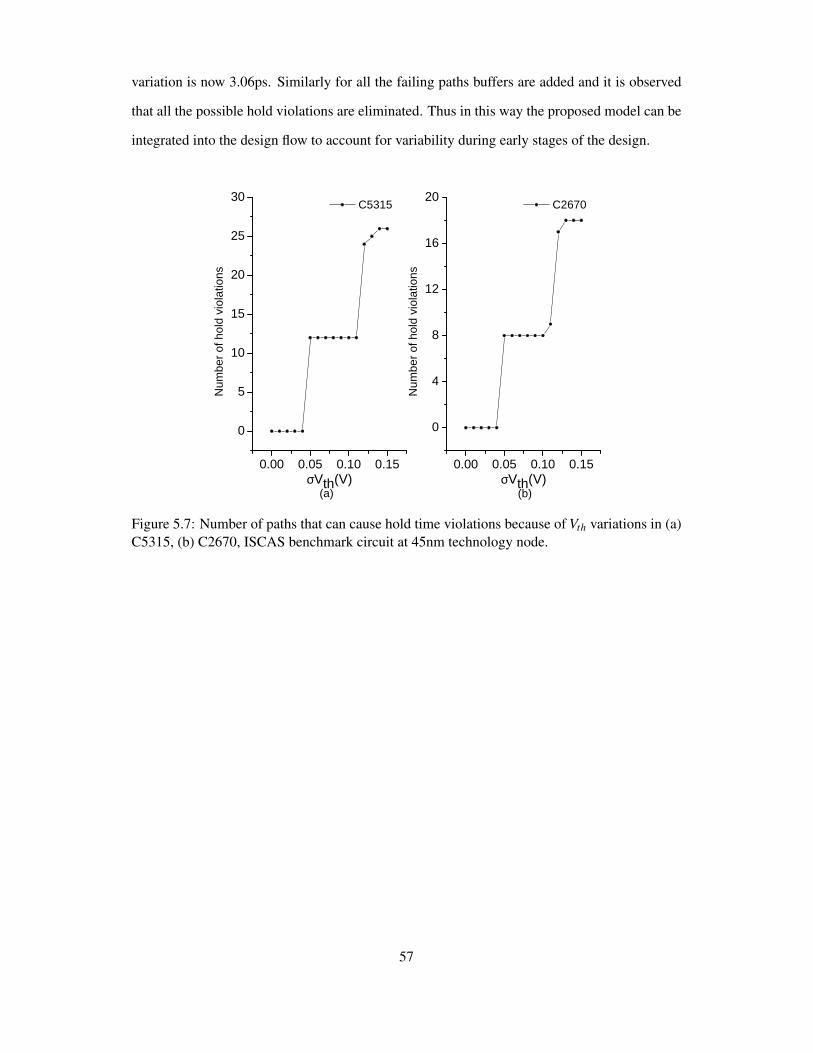
variation is now 3.06ps. Similarly for all the failing paths buffers are added and it is observed
that all the possible hold violations are eliminated. Thus in this way the proposed model can be
integrated into the design flow to account for variability during early stages of the design.
0 . 0 0 0 . 0 5 0 . 1 0 0 . 1 5
0
5
1 0
1 5
2 0
2 5
3 0 C 5 3 1 5Nu
mber
of ho
ld vio
lation
s
σV t h ( V )0 . 0 0 0 . 0 5 0 . 1 0 0 . 1 5
0
4
8
1 2
1 6
2 0
( b )
C 2 6 7 0
Numb
er of
hold
violat
ions
σV t h ( V )( a )
Figure 5.7: Number of paths that can cause hold time violations because of Vth variations in (a)C5315, (b) C2670, ISCAS benchmark circuit at 45nm technology node.
57

Chapter 6
CONCLUSIONS
6.1 Summary
In this thesis, an accurate analytical model to predict nominal delay and delay variability of
CMOS circuits is proposed. The model is comprehensive and enables a quick estimate of
variability for large CMOS circuits. It can be integrated with an existing design flow to facilitate
design of robust circuits in scaled technologies.
First a nominal delay model is developed for an inverter that considers factors such as
gate width, load capacitance and input transition time. The average error compared to HSPICE
simulated results is -1.17% for varying width, load capacitance and input transition time at
45nm technology node. The model is then extended to gates with stacked transistors like NAND
and NOR. In such gates, the delay is also a function of the position of the transistor with switch-
ing input. The average error is 0.31% for varying width, load capacitance and input transition
time at 45nm technology for NAND2 gate.
Next, the model for delay variability because of varying Vth is derived for an inverter.
The variability of a gate is directly proportional to tr except when loaded with large load capac-
itance. The maximum difference between estimated and simulated σ/µ is 1.09% for varying
width, load capacitance and input transition time at 45nm technology. The model is extended
to handle stacked transistors. The maximum difference between estimated and simulated σ/µ
is 1.7% for varying width, load capacitance and input transition time at 45nm technology for
NAND2 gate.
The proposed model is applied to complex gates like XOR and Full adder. Model esti-
mated σ/µ matches HSPICE simulated results within 0.65% error. The model is then applied
to complex ISCAS’85 benchmark circuits. The nominal delay estimates are within 4% differ-
ence when compared to Synopsys primetime estimated results. The variability estimates for
ISCAS’85 benchmark circuits are done with in fraction of time compared to HSPICE simula-
tions. It is also observed that, variability in non-critical paths can be more than that of critical
path and the worst case delay (µ + 3σ ) can be larger for non-critical paths. Also the rate of
possible hold violations increases rapidly with increasing Vth variations. These kind of analysis
58

were quickly done using the proposed model. Using HSPICE would have been impractical.
Thus the proposed model reduces time and effort to analyze variability of complex
circuits without compromising on the accuracy.
6.2 Future Work
The model has been developed for all gates at 45nm technology and for inverter at 32nm tech-
nology. It can be further extended to 22nm, 16nm and 12nm technology nodes. Variability is
high at these technology nodes and Vth variation is not the only cause. Along with Vth variation,
other parameter like width of transistors has to be taken into account. Variations in length and
width become prominent at these technology nodes because of small feature size. The model
can be extended to account for these variations also.
59

REFERENCES
[1] ISCAS’85. http://dropzone.tamu.edu/~xiang/iscas.html.
[2] ITRS. http://public.itrs.net/.
[3] Nangate. http://www.nangate.net/.
[4] PTM. http://ptm.asu.edu/.
[5] M. Alam, K. Kang, B.C. Paul, and K. Roy. Reliability- and Process-Variation AwareDesign of VLSI Circuits. 14th International Symposium on the Physical and FailureAnalysis of Integrated Circuits, 2007. IPFA 2007, pages 17 –25, July 2007.
[6] M. Alioto, G. Palumbo, and M. Pennisi. Understanding the effect of process variations onthe delay of static and domino logic. IEEE Transactions on Very Large Scale Integration(VLSI) Systems, 18:697–710, May 2010.
[7] A. Asenov, A.R. Brown, J.H. Davies, S. Kaya, and G. Slavcheva. Simulation of intrinsicparameter fluctuations in decananometer and nanometer-scale MOSFETs. IEEE Transac-tions on Electron Devices, 50(9):1837 – 1852, Sept. 2003.
[8] A. Asenov, S. Kaya, and J.H. Davies. Intrinsic threshold voltage fluctuations in decananoMOSFETs due to local oxide thickness variations. IEEE Transactions on Electron De-vices, 49(1):112 –119, Jan 2002.
[9] S. Borkar. Circuit Techniques for Subthreshold Leakage Avoidance, Control, and Toler-ance. Proc. Intl Electron Devices Meeting (IEDM 2004), IEEE Press, pages 421–424.
[10] S. Borkar. Designing reliable systems from unreliable components: the challenges oftransistor variability and degradation. IEEE Micro, 25(6):10 – 16, Nov.-Dec. 2005.
[11] E. Cassan, P. Dollfus, S. Galdin, and P. Hesto. Calculation of direct tunnelling gate currentthrough ultrathin oxide and oxide/nitride stacks in MOSFETs and H-MOSFETs. Micro-electron Reliability, 40:585 – 588, 2000.
[12] M. Chandhok, K. Frasure, E.S. Putna, T. Younkin, W. Rachmady, U. Shah, and W. Yueh.Improvement in linewidth roughness by postprocessing. Journal of Vacuum Science Tech-nology B: Microelectronics and Nanometer Structures, 26(6):2265 –2270, Nov. 2008.
[13] B. H. Calhoun et al. Digital circuit design challenges and opportunities in the era ofnanoscale CMOS. Proceedings of the IEEE, 96(2):343–365, Feb 2008.
[14] D. L. Goldfarb et al. Effect of thin-film imaging on line edge roughness transfer to under-layers during etch processes. Journal of Vacuum Science Technology B: Microelectronicsand Nanometer Structures, 22(2):647 –653, Mar 2004.
60

[15] J. Tschanz et al. Effectiveness of Adaptive Supply Voltage and Body Bias for ReducingImpact of Parameter Variations in Low Power and High Performance Microprocessors.IEEE J. Solid-State Circuits, 38(5):826–829, May 2003.
[16] M. Niwa et al. Atomic order planarization ultrathin SiO2/Si(001) interface. AppliedPhysics Letters, 63(5):675 –677, Aug 1993.
[17] S. Borkar et al. Parameter Variations and Impact on Circuits and Microarchitecture. Proc.40th Design Automation Conf. (DAC 03), pages 338–342, 2003.
[18] S. Ghosh, S. Bhunia, and K. Roy. CRISTA: A New Paradigm for Low-Power, Variation-Tolerant, and Adaptive Circuit Synthesis Using Critical Path Isolation. IEEE TransactionsComputer-Aided Design of Integrated Circuits and Systems, 26:1947–1956, Nov 2007.
[19] R.W. Keyes. Physical limits in digital electronics. Proceedings of the IEEE, 63(5):740 –767, May 1975.
[20] P. Liu and Y.B. Kim. An accurate timing model for nano CMOS circuit consideringstatistical process variation. IEEE International SoC Design Conference(ISOCC), pages269–272, 2007.
[21] P. Liu, Y.B. Kim, and Y.L. Lee. An Accurate Analytical Propagation Delay Model ofNano CMOS Circuits. IEEE International SoC Design Conference(ISOCC), pages 200–203, 2007.
[22] T. Mizuno, J. Okumtura, and A. Toriumi. Experimental study of threshold voltage fluctu-ation due to statistical variation of channel dopant number in MOSFET’s. IEEE Transac-tions on Electron Devices, 41(11):2216 –2221, Nov 1994.
[23] S. Nassif, K. Bernstein, D.J. Frank, A. Gattiker, W. Haensch, B.L. Ji, E. Nowak, D. Pear-son, and N.J. Rohrer. High Performance CMOS Variability in the 65nm Regime andBeyond. Electron Devices Meeting, 2007. IEDM 2007. IEEE International, pages 569–571, Dec. 2007.
[24] A. T. Putra, A. Nishida, S. Kamohara, and T. Hiramoto. Random Vth variation induecedby gate edge fluctuations in nanoscale MOSFETs. Silicon Nanoelectronics Workshop,pages 73–74, 2007.
[25] J.M. Rabaey. Digital Integrated Circuits: A Design Perspective. Englewood Cliffs, NJ:Prentice-Hall, 1996.
[26] T. Sakurai and A.R.Newton. Delay analysis of series-connected MOSFET circuits. IEEEJ.Solid-State Circuits, 26:122–131, 1991.
61

[27] T. Sakurai and A.R. Newton. Alpha-Power law MOSFET model and its application toCMOS inverter delay and other formulas. IEEE J. Solid-State Circuits, 25:584–594, 1990.
[28] S. R. Sarangi, B. Greskamp, R. Teodorescu, J. Nakano, A. Tiwari, and J. Torrellas. VAR-IUS: A model of process variation and resulting timing errors for microarchitects. IEEETransactions on Semiconductor Manufacturing, 21:3–13, 2008.
[29] K. Yamaguchi T. Hagivaga and S. Asai. Threshold voltage variation in very small MOStransistors due to local dopant fluctuations. Proc. Symp. VLSI Technol., Dig. Tech. Papers,pages 46–47, 1982.
[30] D. Z.-Y. Ting, E. S. Daniel, and T. C. McGill. Interface roughness effects in ultrathin gateoxides. VLSI System Design, 8:47 – 51, 1998.
[31] Y. Wang and M. Zwolinski. Analytical transient response and propagation delay modelfor nanoscale CMOS inverter. IEEE International Symposium on Circuits and Systems,pages 2998 – 3001, May 2009.
[32] Y. Ye, S. Gummalla, C. Wang, C. Chakrabarti, and Y. Cao. Random Variability Modelingand its Impact on Scaled CMOS Circuits. J. Computational Electronics, pages 108–113,2010.
[33] Y. Ye, F. Liu, M. Chen, S. Nassif, and Y. Cao. Statistical Modeling and Simulation ofThreshold Variation Under Random Dopant Fluctuations and Line-Edge Roughness. IEEETransactions on Very Large Scale Integration (VLSI) Systems, (99):1 –10, 2010.
62