
AN ALGORITHM AND SYSTEM FOR MEASURING IMPEDANCE IN D-Q COORDINATES
163
AN ALGORITHM AND SYSTEM FOR MEASURING IMPEDANCE IN D-Q COORDINATES Gerald Francis Dissertation submitted to the Faculty of the Virginia Polytechnic Institute and State University in partial fulfillment of the requirements for the degree of Doctor of Philosophy in Electrical Engineering Dushan Boroyevich, Chairperson William T. Baumann Rolando Burgos Jack J. Lesko William H. Tranter January 25th, 2010 Blacksburg, VA Keywords: Impedance Measurement, Three Phase AC Systems, Rotating Coordinate Systems, Transfer Functions, Power Electronics, D-Q Coordinates Copyright 2010, Gerald Francis
Transcript of AN ALGORITHM AND SYSTEM FOR MEASURING IMPEDANCE IN D-Q COORDINATES

AN ALGORITHM AND SYSTEM FOR
MEASURING IMPEDANCE IN D-Q COORDINATES
Gerald Francis
Dissertation submitted to the Faculty of the Virginia Polytechnic Institute and State
University in partial fulfillment of the requirements for the degree of
Doctor of Philosophy
in
Electrical Engineering
Dushan Boroyevich, Chairperson
William T. Baumann
Rolando Burgos
Jack J. Lesko
William H. Tranter
January 25th, 2010
Blacksburg, VA
Keywords: Impedance Measurement, Three Phase AC Systems, Rotating
Coordinate Systems, Transfer Functions, Power Electronics, D-Q Coordinates
Copyright 2010, Gerald Francis

An Algorithm and System for Measuring Impedances in D-Q Coordinates
Gerald Francis
ABSTRACT
This dissertation presents work conducted at the Center for Power Electronics Systems
(CPES) at Virginia Polytechnic Institute and State University.
Chapter 1 introduces the concept of impedance measurement, and discusses previous work
on this topic. This chapter also addresses issues associated with impedance measurement.
Chapter 2 introduces the analyzer architecture and the proposed algorithm. The algorithm
involves locking on to the voltage vector at the point of common coupling between the analyzer
and the system via a PLL to establish a D-Q frame. A series of sweeps are performed, injecting
at least two independent angles in the D-Q plane, acquiring D- and Q-axis voltages and currents
for each axis of injection at the point of interest.
Chapter 3 discusses the analyzer hardware and the criteria for selection. The hardware built
ranges from large-scale power level hardware to communication hardware implementing a
universal serial bus. An eight-layer PCB was constructed implementing analog signal
conditioning and conversion to and from digital signals with high resolution. The PCB
interfaces with the existing Universal Controller hardware.
Chapter 4 discusses the analyzer software. Software was written in C++, VHDL, and
Matlab to implement the measurement process. This chapter also provides a description of the
software architecture and individual components.
Chapter 5 discusses the application of the analyzer to various examples. A dynamic model
of the analyzer is constructed, considering all components of the measurement system.
Congruence with predicted results is demonstrated for three-phase balanced linear impedance
networks, which can be directly derived based on stationary impedance measurements. Other
impedances measured include a voltage source inverter, Vienna rectifier, six-pulse rectifier and
an autotransformer-rectifier unit.

iii
To my Mom, my Sister and my
Grandparents for enabling me to
get where I am today.
I love you all!

iv
Acknowledgements
I would like to thank my colleagues at the Center for Power Electronics Systems (CPES). I have
had many conversations and collaboratively investigated many tough questions with many of
them (their questions and my own). They are a valuable resource to the power electronics
community, and working together, we can help to build a better future for everyone!
I would like to thank my project members for their support, including Dr. Fred Wang, Dr.
Sebastian Rosado, Igor Cvetkovic, Sara Ahmed, Zhiyu Shen, Bo Wen, Di Zhang, and Dong
Dong.
I would like to thank my committee and exam members, Dr. William Baumann, Dr. William
Tranter, Dr. Jack Lesko and Dr. Jaime De La Ree. I appreciate their help and the time they have
given me in helping me during my studies.
I would like to thank Dr. Rolando Burgos for his continual help and support throughout my time
in CPES. Rolando has helped me greatly throughout my time in Virginia Tech as a friend,
giving me advice on and working with me to produce papers, as a project member, and as a
committee member.
I would like to give special thanks to my advisor, Dr. Dushan Boroyevich. It is with his help and
support that I have been able to achieve this. Dr. Boroyevich has been my advisor starting in my
undergraduate studies, was my advisor for my Master‟s, and is my advisor supporting my Ph.D.
degree.
I would like to thank my friends and family for always being there and supporting me! I love
you all!
Jerry
All photographs by Gerald Francis.

v
TABLE OF CONTENTS
Chapter 1. Introduction ................................................................................................................... 1
I. Dynamics of Three Phase Systems under Active Loads ......................................................... 1
II. Stability Analysis in the DQ Frame ....................................................................................... 3
A. Objective Statement ........................................................................................................... 5
III. Existing Attempts at Defining and Measuring Stability and Impedances ............................ 6
A. Non-D-Q frame impedance measurements ........................................................................ 7
B. Injection Signals ................................................................................................................. 7
C. Exogenous Frequency Content and Harmonics ................................................................. 9
D. D-Q Frame Alignment ....................................................................................................... 9
E. Measurement System Error Analysis ............................................................................... 10
F. Balancedness..................................................................................................................... 11
G. Multiple Signal Paths ....................................................................................................... 11
H. Other Related Work in Impedance and Identification ..................................................... 11
I. Challenge of Verification .................................................................................................. 12
IV. Summary ............................................................................................................................. 12
V. Dissertation Contents ........................................................................................................... 13
Chapter 2. Algorithmic Solution and System Architecture .......................................................... 15
I. Proposed Algorithm ............................................................................................................... 15
A. System Description and Nomenclature ............................................................................ 15
B. Calculating Impedance – System of Equations ................................................................ 19
C. Calculating Impedance – Linear regression ..................................................................... 20
D. Voltage Perturbation Magnitude Consideration .............................................................. 21

vi
E. Current Perturbation Magnitude ....................................................................................... 22
F. Frequency Content in ABC Domain................................................................................. 23
II. Model of System .................................................................................................................. 23
A. Network Analyzer ............................................................................................................ 24
B. Impedance Tester Model .................................................................................................. 24
C. System Model and Construction ...................................................................................... 25
III. Representing System Dynamics ......................................................................................... 26
A. Single Phase Example ...................................................................................................... 26
B. Application to Three-Phase D-Q Systems ....................................................................... 30
IV. Phase-Locked Loop ............................................................................................................ 31
A. Effect of the Phase-Locked Loop on Impedance Measurement ...................................... 31
B. Locking the PLL............................................................................................................... 32
C. Phase Locked Loop Accuracy and Imbalances ................................................................ 33
V. Summary .............................................................................................................................. 34
Chapter 3. Hardware Implementation Architecture ...................................................................... 35
I. System Architecture .............................................................................................................. 35
II. Overview of System ............................................................................................................. 36
III. Subsystem Key Functions and Interfaces Overview .......................................................... 37
A. Power Processing Subsystem ........................................................................................... 38
B. Signal-Conditioning Subsystem ....................................................................................... 39
C. Control and HMI subsystem ............................................................................................ 39
IV. Power Processing Subsystem – Injection ........................................................................... 40
V. Power Processing Subsystem – Measurement ..................................................................... 41
A. Current Sensors ................................................................................................................ 41
B. Voltage Sensors ................................................................................................................ 44
vii
VI. Cabinet ................................................................................................................................ 48
VII. Signal-Processing Subsystem ............................................................................................ 50
A. – Digital Subsystem - Universal Controller ..................................................................... 51
B. Digital Subsystem – Control System Communication – Hardware and Physical Interface
............................................................................................................................................... 53
C. Analog Subsystem Overview ........................................................................................... 56
D. Analog Subsystem Architecture....................................................................................... 56
E. Analog Subsystem Inputs ................................................................................................. 58
F. Analog Subsystem Outputs............................................................................................... 59
VIII. Control Subsystem ........................................................................................................... 61
IX. Summary and Conclusions ................................................................................................. 61
Chapter 4. Software Implementation Architecture ....................................................................... 63
I. Overview ............................................................................................................................... 63
II. DSP Software ....................................................................................................................... 65
A. Overview .......................................................................................................................... 65
B. Message Loop (Communication) ..................................................................................... 66
C. Interrupt Handler (Algorithm) .......................................................................................... 71
III. FPGA Firmware .................................................................................................................. 72
A. Architecture ...................................................................................................................... 72
IV. Matlab Software – Algorithm and Instrumentation Interface............................................. 74
A. Architecture ...................................................................................................................... 74
B. Algorithm ......................................................................................................................... 74
C. Instrumentation Interface ................................................................................................. 75
D. Data Management Scripts ................................................................................................ 76
V. Matlab Software – GUI and Data Storage ........................................................................... 76

viii
A. Graphical User Interface .................................................................................................. 76
B. Data Storage ..................................................................................................................... 78
VI. USB Interface ..................................................................................................................... 79
A. Short Review of Active-X Controls and COM ................................................................ 79
B. COM as Used in This Architecture .................................................................................. 81
C. USB Active-X Dispinterface ............................................................................................ 82
D. USB Interface Software ................................................................................................... 82
VII. GPIB Interface ................................................................................................................... 83
VIII. Summary and Conclusions............................................................................................... 84
Chapter 5. Verification and Test ................................................................................................... 85
I. Introduction ........................................................................................................................... 85
II. Model of an ABC Domain Transfer Function as Seen in the DQ Space ............................. 86
A. Notation and D-Q representation of three-phase variables .............................................. 86
B. Example Systems ............................................................................................................. 88
C. Symmetrical Transfer functions in the ABC Domain as seeniIn the DQ Domain .......... 89
D. Sinusoidal Modulation in the Frequency Domain ........................................................... 91
E. Application to example ..................................................................................................... 93
F. Properties of Transformed Matrices ................................................................................. 93
G. Application of Field Properties ........................................................................................ 95
H. Symmetrical State Space Models in the ABC Domain as seen In the DQ Domain ........ 95
I. Phase State Space Model Transformation to D-Q ............................................................. 95
J. Extension to Non-Diagonal ABC Domain Transfer Functions ........................................ 97
K. Application to Power Electronics-based Three-Phase Converters and their Elements ... 97
III. Characteristics of System under Test .................................................................................. 99
IV. Tests used to Validate Operation ...................................................................................... 106

ix
A. Passive Stationary Coordinate Measurements ............................................................... 106
B. Calculated Impedances ................................................................................................... 108
C. Test Cases – Balanced Linear Combinations ................................................................. 109
V. Measurements which Observe Impedance of More Complex Modules ............................ 111
A. Unbalanced Conditions .................................................................................................. 112
B. Balanced Impedance Condition ..................................................................................... 112
C. Unbalanced Impedance Condition ................................................................................. 119
VI. Switching Converters – VSI ............................................................................................. 121
A. Architecture .................................................................................................................... 121
B. Properties of the Nominal Impedance of the VSI .......................................................... 122
VII. Six-Pulse Rectifier ........................................................................................................... 126
VIII. ATRU ............................................................................................................................. 133
IX. Summary and Conclusions ............................................................................................... 140
Chapter 6. Summary and Conclusions ........................................................................................ 141
I. Summary .............................................................................................................................. 141
II. Conclusion .......................................................................................................................... 141
III. Future Work and Improvements ....................................................................................... 142
A. Injection Amplifiers ....................................................................................................... 142
B. Algorithm Implementation ............................................................................................. 143
C. Complete real-time data flow in FPGA.......................................................................... 143
References ....................................................................................................................................144

x
List of Figures
Fig. 1-1: Three Phase AC Balanced Waveform .............................................................................. 1
Fig. 1-2: Constant Power Load Characteristic and Linear Approximation Showing Negative
Slope ............................................................................................................................................... 2
Fig. 1-3: Example System with Unit Under Test / Measurement ................................................... 6
Fig. 2-1: System in ABC Coordinates .......................................................................................... 16
Fig. 2-2: System In D-Q Coordinates ........................................................................................... 17
Fig. 2-3: Injecting Current On the D-axis ..................................................................................... 18
Fig. 2-4: Injecting Current On the Q-axis ..................................................................................... 19
Fig. 2-5: System Inputs and Outputs............................................................................................. 24
Fig. 2-6: Network Analyzer Block Diagram................................................................................. 24
Fig. 2-7: Tester Injection and Measurement Unit Interface .......................................................... 25
Fig. 2-8: System Diagram of Tester with Analyzer ...................................................................... 26
Fig. 2-9: Sample System ............................................................................................................... 27
Fig. 2-10: Block Diagram Representation of System ................................................................... 27
Fig. 2-11: Sample impedance with shunt current and load side supply removed ......................... 28
Fig. 2-12: Block diagram of example with perturbation and load side supply removed. ............. 28
Fig. 2-13: Injecting Shunt Current Into Example ......................................................................... 29
Fig. 2-14: Simplified Block Diagram Representing Shunt Injection into Example ..................... 29
Fig. 2-15: Block Diagram Representation of System Under Test ................................................ 30
Fig. 2-16: Typical D-Q Phase Locked Loop ................................................................................. 31
Fig. 2-17: Dual Decoupled Synchronous Reference Frame based PLL ....................................... 33
Fig. 3-1: System Block Diagram .................................................................................................. 37
Fig. 3-2: Subsystem Definitions ................................................................................................... 38
Fig. 3-3: Power Processing Subsystem Showing Interfaces 1 and 2 ............................................ 40
Fig. 3-4: Injection Reference to Injection Current ........................................................................ 41
Fig. 3-5: Current Sensors .............................................................................................................. 43
Fig. 3-6: Current Sensor Frequency Response (Negative reference) .......................................... 43
Fig. 3-7: Original Voltage Sensor ................................................................................................. 44
Fig. 3-8: Original Voltage Sensor Response (Gain of sensor normalized)................................... 45

xi
Fig. 3-9: New Custom Voltage Sensors ........................................................................................ 46
Fig. 3-10: Voltage Sensor Transfer Function vs Tektronix Probe ................................................ 47
Fig. 3-11: Injection Hardware Cabinet ......................................................................................... 49
Fig. 3-12: Injection Hardware Cabinet Lower Stage .................................................................... 50
Fig. 3-13: Signal Processing Subsystem ....................................................................................... 51
Fig. 3-14: Universal Controller Functional Block Diagram ......................................................... 52
Fig. 3-15: Universal Controller ..................................................................................................... 53
Fig. 3-16: USB Interface Schematic ............................................................................................. 55
Fig. 3-17: Analog and USB Interface with Universal Controller Mounted On Top .................... 57
Fig. 3-18: Analog Measurement PCB Architecture (Excluding USB Interface) .......................... 58
Fig. 3-19: Analog Output Stage Schematic .................................................................................. 61
Fig. 4-1: Software Architecture .................................................................................................... 65
Fig. 4-2: USB Custom Command Packet for Controller Application Communication ............... 68
Fig. 4-3: Signal flow diagram for interrupt handler ...................................................................... 71
Fig. 4-4: SPI Bus Interface VHDL Block Diagram ...................................................................... 73
Fig. 4-5: Sweep Process and Messaging ....................................................................................... 75
Fig. 4-6: Graphical User Interface ................................................................................................ 77
Fig. 4-7: Currents as displayed on current tab. The currents are those used to measure the
impedance which is selected in the first tab, labeled Results Viewer. ......................................... 78
Fig. 4-8: Directory Structure of Impedance Measurement Software ............................................ 79
Fig. 4-9: Software used to set UC parameters directly via USB. The parameters sent to the
controller can be seen in the grid on the left hand side. The parameters may be changed using
the controls in the group box labeled Set, and read by pressing Acquire. The USB Active-X
control can be seen in the lower right hand corner. ...................................................................... 83
Fig. 5-1: DQ Representation of ABC domain Transfer Function ................................................. 87
Fig. 5-2: System Represented in DQ Coordinates ........................................................................ 88
Fig. 5-3: Transforming to ABC Coordinates and Applying H ..................................................... 89
Fig. 5-4: Applying Hdq and Transforming to ABC Coordinates ................................................. 90
Fig. 5-5: System Block Diagram ................................................................................................ 100
Fig. 5-6: Modified Block Diagram with All Inputs and Outputs ................................................ 103
Fig. 5-7: Simplified System ........................................................................................................ 104

xii
Fig. 5-8: Measured line-to-neutral impedance and 10th-order state-space approximation ........ 108
Fig. 5-9: Passive Impedance Test Setup ..................................................................................... 109
Fig. 5-10: Passive Impedance Test Results - RLC Test, Zdd and Zqq ....................................... 110
Fig. 5-11: Passive Impedance Test Results - RLC Test, Zdq and Zqd ....................................... 111
Fig. 5-12: Stationary Frame Measurements of RLC Impedance ................................................ 113
Fig. 5-13: Actual Zdd and Zqq Impedances Compared to Measured Impedances ..................... 114
Fig. 5-14: Actual and Measured Zdq and Zqd Impedances ........................................................ 115
Fig. 5-15: Actual and Filtered Zdd and Zqq Impedances ........................................................... 116
Fig. 5-16: Actual and Filtered Zdq and Zqd Impedances ........................................................... 117
Fig. 5-17: Current Sensor Response Voltages Transformed to the D-Q frame. The actual
currents are 15 times larger than the sensor‟s output. ................................................................. 118
Fig. 5-18: Load Voltage Response In To DSP Showing Significant Reduction At High
Frequencies. The actual voltages are 51 times larger than the sensor‟s output. ........................ 119
Fig. 5-19: Zdd and Zqq for Unbalanced Impedances ................................................................. 120
Fig. 5-20: Zqd and Zdq for Unbalanced Case ............................................................................. 121
Fig. 5-21: Voltage Source Inverter Block Diagram With Control Components ........................ 122
Fig. 5-22: Simulated impedance of the VSI when measured with D-Q frame aligned with the D-
axis and aligned with an offset of 10 degrees from the D-Axis. The impedances are coincident as
per the model............................................................................................................................... 123
Fig. 5-23: Simulated Impedances for Asymmetrical Control of the Voltage Source Inverter ... 124
Fig. 5-24: VSI Measured and Simulated Impedances: Zdd (Upper Left), Zdq (Upper Right), Zqd
(Lower Left), Zqq (Lower Right). The two simulations are two different IF bandwidth choices.
The PLL is aligned with the D-axis voltage, and the Q-axis is running in open-loop. ............... 125
Fig. 5-25: VSI Impedance when aligned on the Q-Axis: Zdd (Upper Left), Zdq (Upper Right),
Zqd (Lower Left), Zqq (Lower Right). The two simulations are two different IF bandwidth
choices. The PLL is aligned with the D-axis voltage, and the Q-axis is running in open-loop. 126
Fig. 5-26: Diode rectifier driving programmable load ................................................................ 127
Fig. 5-27: Six-pulse rectifier waveforms showing ABC voltages in the first graticule (at 50 volts
per division), ABC currents in the second graticule (at 2 amps per division), and - currents in
the third graticule (also at 2 amps per division). The fourth graticule shows the trajectory of the
current on the - plane. All waveforms vs. time are scaled to 500 S per division................ 128

xiii
Fig. 5-28: Zdd for six-pulse rectifier showing results for constant current (CI), constant power
(CP) and constant resistance (CR) for two different power levels. ............................................ 129
Fig. 5-29: Zqq for six-pulse rectifier showing results for constant current (CI), constant power
(CP) and constant resistance (CR) for two different power levels. ............................................ 130
Fig. 5-30: Zdq for six-pulse rectifier showing results for constant current (CI), constant power
(CP) and constant resistance (CR) for two different power levels. ............................................ 131
Fig. 5-31: Zqd for six-pulse rectifier showing results for constant current (CI), constant power
(CP) and constant resistance (CR) for two different power levels ............................................. 132
Fig. 5-32: Six-pulse constant current response with capacitors and inductors shown................ 133
Fig. 5-33: ATRU Test setup showing source on left, followed by a source side resistor
impedance of 0.6 Ohms followed by the injection hardware followed by the ATRU and load. 134
Fig. 5-34: ATRU waveforms showing ABC voltages in the first graticule (at 50 volts per
division), ABC currents in the second graticlule (at 2 amps per division), and - currents in the
third graticule (also at 2 amps per division). The fourth graticule shows the trajectory of the
current on the - plane. All waveforms vs. time are scaled to 500 S per division................ 135
Fig. 5-35: ATRU Zdd showing results for constant current (CI), constant power (CP) and
constant resistance (CR) for two different power levels. ............................................................ 136
Fig. 5-36: ATRU Zdq showing results for constant current (CI), constant power (CP) and
constant resistance (CR) for two different power levels. ............................................................ 137
Fig. 5-37: ATRU Zqd showing results for constant current (CI), constant power (CP) and
constant resistance (CR) for two different power levels. ............................................................ 138
Fig. 5-38: ATRU Zqq showing results for constant current (CI), constant power (CP) and
constant resistance (CR) for two different power levels. ............................................................ 139
Fig. 5-39: ATRU DC Link and Zdd ........................................................................................... 140

xiv
List of Tables
Table 4-1: DSP Shared Parameters ............................................................................................... 67
Table 4-2: Index Parameters ......................................................................................................... 70
Table 5-1: Transfer Function Description ................................................................................... 100

1
Chapter 1. Introduction
Three-phase AC systems are often used at the kilowatt power level and above, providing
three electrical conductors delivering power. Most often, the three voltage waveforms form
sinusoidal patterns, phase-shifted by 120 degrees, as depicted below.
Fig. 1-1: Three Phase AC Balanced Waveform
Three-phase power electronics-based converter interface systems are used to provide power
to loads, to provide filtering functions, and to convert between forms of electrical energy.
Examples are three-phase inverters, three-phase rectifiers, three-phase motor drives, three-phase
AC-AC converters, and three-phase active filters.
I. Dynamics of Three Phase Systems under Active Loads
As power electronics technology infiltrates the power processing and generation field, it
introduces the opportunity, requirement, and consequences of applying closed-loop control.
There exists now the opportunity to control power flow and improve the quality of the delivered
power. The converters are nonlinear, and their dynamics are coupled with those of the load and
source systems they provide power to and take power from. As a consequence, many power
electronics systems require control to provide a regulated output. With this regulation, however,
comes new phenomena that were not previously seen in the power system, and as such it
introduces new perils, including, but not limited to, threatening the stability of the power system
[1].
References [1-5] show that power electronics converters with regulated output control
provide negative incremental impedance characteristics at their input. Such systems regulate the
output voltage, and at a fixed current they consume constant power. If the power electronics

2
converter is perfect and lossless, the input will also have a constant power characteristic, upon
which linearizing provides a negative slope at its operating point, as shown in Fig. 1-2.
i
v
v0
o
iv
lin viii
vv 0
, 00
i0
iiv
1)(
Fig. 1-2: Constant Power Load Characteristic and Linear Approximation
Showing Negative Slope
While our larger national power grid can tolerate many of these behaviors, as their effect is
small compared to the size of the system, many smaller systems cannot. Some small systems
contain their own power source, and are not directly connected to the near-infinite busses
presented by the national power grid. Examples of such systems are aircraft in the air [6-8],
ships at sea [9-13], hybrid-electric vehicles [14-16], and small islands with small power
processing plants. Sometimes systems are connected to equipment such as frequency changers,
AC/DC converters and other hardware. Examples of these connected systems are aircraft on the
ground or on an aircraft carrier connected to the airport or ship‟s grid [17]. The aircraft
examples also have another phenomenon – both have local systems operating at higher line
frequencies ranging from more than 300 Hz to 800 Hz instead of the traditional 50 and 60 Hz
typically encountered. These higher line frequencies provide additional challenges relating to
control.
These systems are becoming more and more prevalent in our society, changing functions that
were previously implemented with hydraulic and mechanical systems to implementation with
electrical systems, and as a consequence it is imperative that we are able to predict and test their

3
safe operation. Furthermore, they are being integrated into vehicular platforms under which
stability concerns are greater due to the small power sources. This is not the first time power
electronics have introduced this challenge of interconnected system stability, however. The use
of DC/DC converters in distributed power systems other than DC distribution systems received a
lot of attention in the past. Solutions are available for DC systems [18], but for the systems
discussed in this paper, there are issues not seen in DC systems that prevent direct application of
these methods.
II. Stability Analysis in the DQ Frame
The power system interfaces with devices used to control power flow in order to provide
power to the load, which consists of three-phase power converters. Analysis of these devices
and systems can be performed at multiple levels, ranging from power flow and power quality all
the way to models of the solid-state semiconductor devices in the converters themselves.
Appropriate models are chosen based on the level of analysis to be performed [19]. As this
report focuses on measuring impedance as a function of frequency, the models will be small-
signal models representing the converter and subsystem behavior at a given operating point.
The loads of these power electronic systems, being mechanical or electrical, tend to have
dynamic properties (states), and the power conditioning equipment itself contains elements with
dynamic properties, such as inductors and capacitors, in addition to controllers which introduce
additional states and delays. The converters themselves (and thus the aggregate systems)
generally comprise a set of nonlinear dynamics, and in the case of power electronics, these are
also non-smooth, right-hand-side discontinuous nonlinear differential equations. Power
converter modeling approaches commonly used today have methods to smooth out these right-
hand-side discontinuities [20, 21] and provide Lipschitz systems to the user for analysis,
simplifying the model of the converter to one with continuous, but usually still nonlinear system
dynamics. Although these systems have been simplified by such models, they remain
challenging to analyze, often providing multiple stability points (and therefore basins of
attraction), and a series of other nonlinear phenomena, ranging from bifurcation to limit cycles
and chaos [22, 23]. Furthermore, such nonlinear systems operate on a nominal trajectory in
steady-state, nominally given by (1)

4
, , (1)
making them non-stationary systems with periodic tendencies.
To simplify analysis, attempts have been made, to map this non-stationary system and its
components to one which is stationary [24], mitigating (but unfortunately not completely
eliminating in practice) the non-autonomous nature of such systems. To transform the system,
the three voltages can be represented as a voltage vector which rotates in three-dimensional
space. If the voltage vector follows the trajectory given in (1), it will trace a circle at a constant
frequency of radians per second. A rotating coordinate system can be defined that matches the
frequency of rotation of the voltage vector, making the voltage appear stationary in that frame.
This transformation is shown in (2).
(2)
For the systems in this dissertation, the third component, the 0-axis, can be ignored. If the
system is always balanced, this axis is identically zero for all time.
For linear analysis of nonlinear systems, it is necessary to have an operating point upon
which to perform linearization. When the system is unbalanced, this operating point disappears
when using the map described above, and the system cannot be linearized, and thus classical
stability analysis becomes difficult without further tools. If the three voltages follow the
trajectory specified in (1) then the resulting vector in the D-Q frame, calculated by applying (2)
will be
(3)
Systems of loads and sources, although stable individually, may become unstable when they
are interconnected. Stability in the D-Q frame has been explored previously in [4, 25, 26] for
systems whose impedance is known. Based on the analysis methods provided in these papers,
one may predict whether the interconnection of two power electronics subsystems at an
operating point will produce a stable system. In order to apply these methods in practice, it

5
becomes necessary to be able to measure the impedance to which to apply the criteria discussed
in these works.
This is not an easy task. Nearly all systems are nonlinear, and as such, require an operating
point in order to take a measurement. This requires the system to be operating during the
measurement. The fact that most of these converters are designed for a high power level
precludes the use of most commercially available equipment used to measure impedance via
traditional means, such as the Agilent 4394. This equipment can take highly accurate
measurements, but at very low power levels. For linear time-invariant, balanced networks, this is
not a requirement, but for nonlinear systems, unless the impedance can be transformed a
posteriori, it is necessary to be at the system operating point. For nearly all systems that involve
power electronics equipment, this is a requirement.
This restriction gives rise to several challenges in implementing a measurement system for
this kind of subsystem. The first challenge is the ability to induce a perturbation into a system.
Such an injection must be supplied at a reasonable magnitude in order to perturb the system, and
the injection equipment must be able to operate with other large power sources active in the
system.
Furthermore, unlike traditional analyzers, this analyzer must measure the impedance in an
artificial frame of reference that does not physically exist. There are no D- and Q- axis terminals
to which one may connect a sensor, and the reference frame must be derived via real-time
processing.
A. Objective Statement
The objective of this work is to produce a set of requirements for an instrument that can be
used to measure the frequency-dependent AC impedance of a subsystem (on either load side or
source side) in the D-Q synchronous rotating reference frame during its operation. This report
addresses the components required to measure these impedances and the algorithm of the
measurement unit. These findings are this work‟s primary contribution to the field.

6
III. Existing Attempts at Defining and Measuring Stability and Impedances
Despite the pronounced need for a method to measure impedances, the problem has gone
unsolved. Several works have approached components of this problem, but no one study has
completely addressed all the critical issues presented, and the actual works presenting
experimental data are limited to a few that provide incremental contributions to the
understanding of these challenges. Nearly all of the studies published on this topic, however,
present simulated results.
An example system can be represented as Fig. 1-3. A source system supplies a converter,
which supplies a load. The input impedance and output impedance of the converter can be
measured. In the case of a DC-DC converter, many methods have been made available to do
so[27].
Source
Subsystem
Unit Under
Test (UUT)
Load
Subsystem
i4
v2
+
-
v3
+
-
v1
+
-
v4
+
-
i1 i3i2vp1 vp2
ip1 ip2
Fig. 1-3: Example System with Unit Under Test / Measurement
The nonlinear nature of these systems require them to be running when measured, and
therefore most attempts have provided methods for doing so. Without the challenge of a rotating
coordinate system, analyzers can be directly connected to amplifiers or coupling networks which
couple the perturbation via one of the sources shown in Fig. 1-3.
To create a perturbation in an interface, a series voltage source, current source, or a series- or
shunt-configured impedance may be used. These devices modify the system currents and
voltages in order to create a perturbation. It should be noted that the location at which the
system is perturbed is not necessarily the same as where the perturbation is measured. That is,
ip2 may be used to create a perturbation while i1 and v1 are being measured. The sources in Fig.
1-3 are not in the system, but are placed within the model for the purpose of measuring

7
impedances within the system via injection hardware. One may wish to reference [21] for the
details.
A. Non-D-Q frame impedance measurements
Several works have measured the impedance of the power system as seen from the wall. In
this measurement, a perturbation is injected (without reference frame translation), and several
data points are taken [28-30]. In these measurements, the line voltage acts more as a
disturbance, and is not used as part of the measurement. This method is then repeated to get the
three-phase impedances.
Some works measure the frequency response only at the harmonics of the line, and then
reference this measurement as harmonic impedance (not to be confused with harmonic transfer
functions like those found in [31] that cause responses to be shifted in frequency). Most of this
work has not been driven by stability, but by transient performance and harmonics.
Approaches to measuring the impedances range from the use of a network analyzer [29, 32-
34] to the use of power spectral density techniques via Matlab implementation of Welch‟s
averaged periodogram [35, 36], to transient-fitting techniques via the extended Prony Method
[35, 37-39].
B. Injection Signals
When measuring impedance or admittance, which is a small-signal phenomenon, one must
measure an input (current or voltage) and an output (voltage or current). For a linear system (or
a nonlinear system that is linearized about an operating point), the input and output signal
components at the same frequency are related by a transfer function which defines the gain and
phase shift at that frequency. In order to measure this kind of transfer function, there must be
measurable quantities at that frequency in the input and output signal. In the case of very large
systems, where it may be difficult to explicitly create such a sinusoidal perturbation, the
frequency content may be generated by events such as transients caused by load connections and
disconnections, or other activity in the system not created for the purpose of measurement [33].
It is, however, possible in smaller systems, such as those of interest in this report, to be able to
cause a perturbation into the system.

8
While possible, this is not a small task within itself. There are many challenges with such an
injection. Irrespective of what it should look like, the first challenge is how to safely cause a
perturbation. This problem can be solved with methods including injection via power
converters, machines, and modulated impedances.
In [40], a power converter was used to generate a perturbation into the system on all three
phases. A voltage source inverter was attached to the system, and was provided power on the DC
side from an external source. The converter was shunt connected to the power system.
Activating the converter switches allowed the converter to inject current into the system.
The paper also mentioned that the technique may be performed using an active filter, but did not
demonstrate this. The results in this paper were simulated. It should be noted that while some of
the papers I‟ve studied refer to the injection topology as a measurement technique, this has
nothing to do with the actual measurement itself, but is instead related to creating a perturbation,
not processing the results or determining the injection signal used to acquire the impedance.
Reference [40] claims that the switching frequency of the voltage source converter has to be an
unspecified number of times higher than the highest frequency component of the injected signal.
The claim is, however, substantiated by neither analysis nor reference.
Reference [40] also describes a case where a wound-rotor induction machine was used to
inject a perturbation into the system. In this dissertation, DC current is injected into the machine
and the machine is allowed to spin up to speed and synchronize with the system, after which the
perturbation can be injected on top of the DC signal. A disadvantage this paper discusses below
is that the induction machine must be sized for each application and power level. The machine
injects onto all three phases as it rotates.
A third technique modulates a three-phase shunt-connected resistive impedance using a
three-phase chopper circuit [41]. This injection is made smoother with the addition of a series
inductor. A power semiconductor switch shorts one resistor to create the modulation.
A similar method to inject modulates an impedance only between two of the three phases
[42]. Unlike the previous injection methods, this last injection does not make use of a three-
phase symmetrical injection. It should be noted that here also the results were demonstrated via
simulation. This technique has been patented by Belkhayat [43].

9
Another injection method mentioned by [41] not implemented is a series voltage injection. It
is acknowledged, however, that this is less practical due to the large currents present in the
system.
The converter-based perturbation methods above were directly connected to the system. If
isolation is desired, or if the electronics used are insufficient to inject a signal of proper
magnitude, the use of a transformer may be warranted. Using a transformer does impose
additional restrictions on the injected frequency content, as we discuss below.
C. Exogenous Frequency Content and Harmonics
While injection itself is a challenge, a second challenge involves the presence of exogenous
signals in the network during measurement. Since the network is nonlinear, it is measured
during operation. As such, there are other exogenous signals present due to the system‟s
operation. These include, but are not limited to line frequency harmonics [44], switching ripples,
low-frequency modulation effects [45, 46], zero-crossing distortions due to the non-ideal
behavior of diodes and diode rectifier bridges [47, 48], and load-source interactions [49]. These
low-frequency effects make measurement more difficult, as they are not caused by the injected
perturbation. While attempts have been made to mitigate these effects [50], they still prevail in
many systems.
D. D-Q Frame Alignment
In the D-Q frame, an alignment is chosen which defines the frame. Most work aligns either
the D-Axis or the Q-Axis to the rotating voltage vector. If the D-Q frame is aligned to a different
angle, the impedance may also change [4]. This property that shows no change when changing
the alignment angle is referred to as isotropism or rotational invariance. If a system‟s impedance
is dependent on the alignment of the D-Q frame, the impedance is considered to be anisotropic.
Therefore, for anisotropic systems, it is necessary that the D-Q coordinate system is aligned
properly with the variable of interest. In this report, the D-Q frame will be aligned with the D-
axis such that the Q-axis voltage component is centered on zero, and unless specified otherwise,
all impedances will be defined using this convention.

10
This alignment is usually achieved via a phase-locked loop (PLL) that controls the reference
frame angular velocity until it aligns with the rotating voltage vector. However, if the voltage
vector has harmonics or noise, or if there are unbalances in the system created by the system
itself or by the injected perturbation, the PLL will have a reaction to it, and the frame will no
longer rotate at a constant frequency. Some approaches did not use a PLL, but instead used a
low-pass filter on the line voltage, which will be even more significantly affected by these
harmonics and other exogenous signals, as the basis voltage will now contain low-frequency
perturbation signals. So far, no discussion of the PLL has been presented in the literature for the
purpose of impedance measurement. However, several PLL designs have been found to be
robust to the presence of unbalance [51]. In the case of [40], there is no PLL, and the induction
machine used aligns itself using a DC injected signal, and is therefore subject to the same frame
variation by the system during the AC injection [3].
E. Measurement System Error Analysis
So far no paper has been published with regards to error analysis for these measurements,
although in [28] the repeatability of the measurements was briefly discussed, providing error
bands based on statistical variation of 30 repeated measurements. Each technique has several
computations, and each sensor has errors. It is possible to analyze the errors and how they
propagate through the system. It is important to discuss error when designing a measurement
system, and it remains an open question as to how much error is in the computed impedance
based on what is measured in the actual system. The only way to improve such systems and to
analyze their correctness is to systematically identify the sources of error and their effect on the
reported measurement results.
Typical errors in measurement can come from quantization, sensor nonlinearities, noise,
offsets, and frequency drift of the system, as well as components of the analog-to-digital
conversion such as power supplies. A model of the system must be constructed including an
analyzer that shows how the errors contribute to the output. These errors may not be obvious, as
the transformation to rotating coordinates will provide a frequency shift, and the multi-input,
multi-output nature of the system allows opportunities for these errors to cross-couple between
channels, further complicating the analysis.

11
The valid ranges of the measurement systems presented are also never validated. This is due
to the fact that most are simulated and most simulations use ideal sources and sensors without
quantization or sampling, whereas one would find practical issues in implementing a system for
measurement.
F. Balancedness
While ideal conditions specify that a system in stationary coordinates maps to a point in the
D-Q domain at which linearization can occur, no analysis has been performed based on how
much variation is tolerable, or to what extent the system remains linear despite this time-
variation. Many works have been done presenting phasor and impedance measurement for the
purpose of protective relaying in power systems, to which the issue of balancedness has been
thoroughly addressed; but this measurement is mostly at the synchronous frequency of the
system, and the impedances are measured via phasors. Alternatively, harmonic impedances have
been identified using a Hilbert transform [52].
G. Multiple Signal Paths
As there are two channels, d and q, the impedances are matrices, and there is coupling
between the load and source subsystems via these. A perturbation on the D-channel can cross-
couple to the Q-channel output, which can then interact with the load, and again cross-couple to
produce a voltage response back on the D-channel. This interaction makes the impedance appear
to include the load, and is a result of having a multivariable system. The solution must decouple
this interaction.
H. Other Related Work in Impedance and Identification
Many authors also have algorithms to extract parameters from the system to fit a
predetermined system model. While this is not black-box impedance measurement, it is
noteworthy in this report, as it is another technique used to acquire actual data to fit a model of
the system. It is, however, not as accurate as individual point measurements. Such work can be
found in [53].

12
Additional work has been done on the capture of dynamics via artificial recurrent neural
networks in the D-Q coordinate system [54-56]. These works inject noise into the system and
learn and record the response of the noise to the dynamics. The system input-output relationship
can then be extrapolated from the response. This approach has the advantage in that if the
network is trained properly, it can filter out exogenous noise from the measurements. Although
this approach does capture the dynamics, it does not discuss how to extract the impedance from
the dynamic results, and focuses mostly on the network itself. It should be noted that all three
works cited are only simulated. There is no discussion on the error of the approximation.
I. Challenge of Verification
An additional challenge that arises when building a measurement system is the ability to
verify the measurements are correct. As presented in this work, in the case of linear networks it
is possible to derive the expected D-Q impedances given symmetric, linear, time-invariant
impedances of each phase in stationary coordinates. It should be noted that no published result
that conducted experimental work verified the full impedance they were measuring against
known impedances by measuring them using dedicated equipment. The closest to this was a
low-order parametric model constructed using nominal parameters of a load inductance and
resistance.
For other systems, such as voltage source inverters, creating an approximate model is a well-
known way to represent the system dynamics under ideal conditions [24]. However, this
approximate model derived from ideal switching behavior, and is not without assumptions. It is
important to know for verification purposes that the model is accurate and represents the true
converter‟s behavior despite the presence of other time-varying and nonlinear behavior, such as
converter dead-time and the potential discontinuous conduction of each phase around the zero
crossing.
IV. Summary
The need to know the system impedance has been made apparent based on system stability
requirements, which have become important recently based on the ever-increasing demand of
equipment with destabilizing effects on their host systems. These motivations are amplified by

13
the increasing number of small systems with limited power generation capability and the
increased transition of former hydraulic and mechanical systems to electrical power.
Attempts to measure three-phase impedances have been incomplete. The results that have
been presented thus far do not provide confidence that the measurements are being performed in
an approach acceptable for all load types, especially loads containing power converters. Reasons
for this include a series of issues related to D-Q frame alignment, nonlinear load behavior, multi-
channel power flow, and a range of exogenous signals preventing successful and complete
measurement.
Furthermore, no published work has attempted to characterize their measurement system for
accuracy. As the objective is to formulate a measurement instrument, it is essential to know its
boundaries and capabilities to avoid trusting incorrect measurements. Additional work is
required in order to understand these characteristics and capabilities.
V. Dissertation Contents
Chapter 1 has provided a summary of the literature on predicting perturbations in three-phase
AC systems. Chapter 2 addresses the proposed algorithmic solution and verifies it in simulation.
In this chapter it will be seen that the algorithm can be validated by constructing an analyzer in
simulation which builds a frequency response table. The frequency response is then post-
processed in Matlab to calculate impedances. The system as a whole is discussed here, defining
interfaces in the D-Q domain and discussing the architecture of a solution.
Chapter 3 addresses the hardware implemented as part of the solution to implement the
impedance tester outlined in Chapter 2. It discusses the hardware hierarchical architecture, and
reviews all of the hardware used, from the power hardware used in the injection, to signal-
processing elements implemented on custom-printed circuit boards, to the sensors used. Critical
characteristics of each element are discussed here, including THD, harmonic content and
nonlinearities.
Chapter 4 addresses the software implemented as part of the solution. The software is
hierarchical just like the hardware, with supervisory software running on a PC that
communicates to a DSP, which runs real-time transformations and signal conditioning. Software

14
elements are written in VHDL to implement communication drivers for exchanging data with
serial peripheral interface equipment. Additional software is written describing the presentation
of results to the user of the instrument and the management of stored results for future use.
Chapter 5 validates the tester with known impedances and explores additional impedances,
such as that of a voltage source inverter, a six-pulse rectifier, an 18-pulse auto-transformer
rectifier unit, a Vienna-type boost power factor correcting rectifier, and an unbalanced linear
load. Additional error analysis and validation is shown in this chapter, along with the
characterization of the measurement equipment.
Chapter 6 concludes and summarizes the work. Propositions for future architectural and
functional improvements are made here.

15
Chapter 2. Algorithmic Solution and System Architecture
Given the challenges shown described in Chapter 1, a solution is proposed which finds the
equivalent impedances of the D-Q system. As will be shown in this chapter, the system will be
perturbed in the D-Q domain, and all voltages and currents at the interface perturbed will be
measured. From a set of responses based on these perturbations, the matrix impedance in the D-
Q frame will be calculated. During this, the reader will be exposed to issues such as the
limitations of measurement equipment and synchronization of the measurement system with the
D-Q frame.
I. Proposed Algorithm
A. System Description and Nomenclature
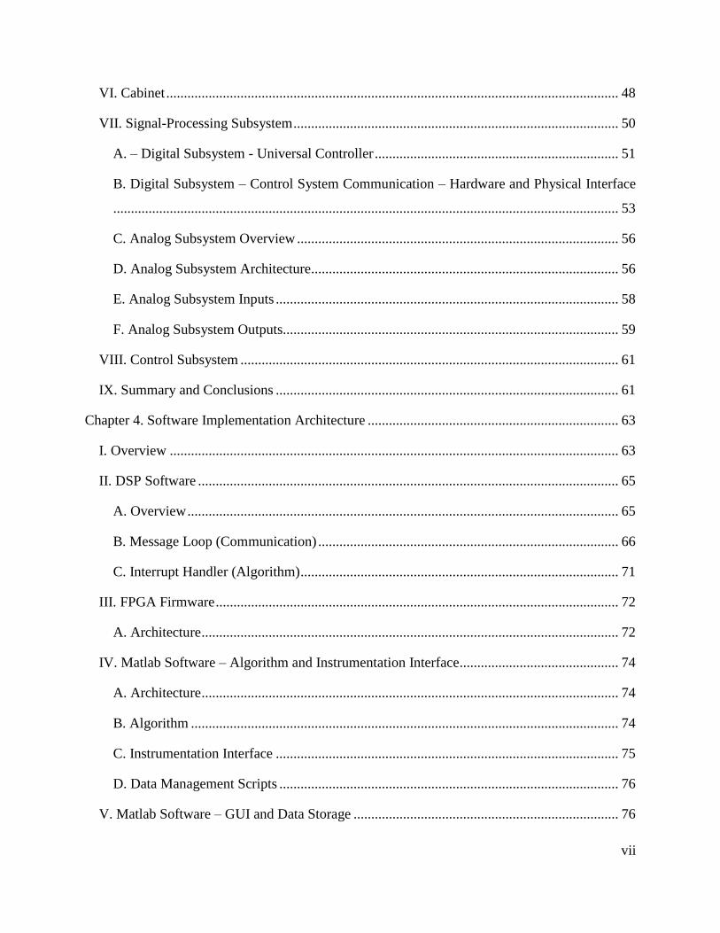
A load and a source interconnected in a three-phase system may be represented by the
following model shows in Fig. 2-1 in ABC coordinates. Adding a perturbation to every phase at
the point of common coupling between the load and the source can be represented using the
Thévenin-equivalent model in Fig. 2-1.
16
ZSa(s)
ZSb(s)
ZSc(s)
ZLa(s)
ZLb(s)
ZLs(s)
iLa
iLb
iLc
iSa
iSb
iSc
iPciPbiPa
van
vbn
vcn
All voltages are with respect to the neutaral, n.
n
vsa
vsb
vsc
Th
eve
nin
Eq
uiv
ale
nt S
ou
rce
Mo
de
l Th
eve
nin
Eq
uiv
ale
nt L
oa
d M
od
el
Fig. 2-1: System in ABC Coordinates
Assuming vsa, vsb, and vsc are symmetric and the source and load are balanced, the equivalent
system in the D-Q frame will appear as follows, where vsd and vsq are constant, as shown in Fig.
2-2.

17
iSdZSdd(s)
ZSdq(s) iSq
vSd
iLd ZLdd(s)
ZLdq(s) iLq
ipd
iSqZSqd(s)
ZSqd(s) iSd
vSq
iLq ZLqq(s)
ZLqd(s) iLd
ipq
Fig. 2-2: System In D-Q Coordinates
Here, the three-phase source and load have been transferred to dual channels (D- and Q-axes)
with matrix impedances to allow both the primary axis and cross-coupling impedances, which
are seen even for simple non-resistive linear circuits.
Injection on one axis, either D, or Q, will lead to currents and voltages on both axes. One
may record these responses. From the cross-coupling terms, there will be interactions from one
channel to the other, which couples to the opposite subsystem. This is shown below, where the
mechanism of coupling the load to the source via the opposite channel is shown via the curved
arrows in Fig. 2-3.

18
iSdZSdd(s)
ZSdq(s) iSq
iLd ZLdd(s)
ZLdq(s) iLq
ipd
iSqZSqd(s)
ZSqd(s) iSd
iLq ZLqq(s)
ZLqd(s) iLd
pd
Sd
i
i
pd
Sq
i
i
vd
vq
pd
q
i
v
pd
d
i
v
Fig. 2-3: Injecting Current On the D-axis
Correspondingly, one may repeat the procedure on the Q-axis and obtain current and voltage
responses on the Q-axis, as shown in Fig. 2-4.

19
iSdZSdd(s)
ZSdq(s) iSq
iLd ZLdd(s)
ZLdq(s) iLq
ipq
iSqZSqd(s)
ZSqd(s) iSd
iLq ZLqq(s)
ZLqd(s) iLd
pq
Sd
i
i
pq
Sq
i
i
vd
vq
pq
q
i
v
pq
d
i
v
Fig. 2-4: Injecting Current On the Q-axis
A critical fact to note here is that since all the impedances are small-signal measurements and
the transfer functions obtained are small-signal phenomena, we can use the principle of
superposition. For a successful measurement, our system must remain the same across multiple
injections if we are to excite them several times, and thus we require the D-Q system to be time-
invariant during this injection, implying that without perturbation, the trajectory of the current
and voltage vectors on the D-Q plane can be mapped to a point. As such, we can measure these
transfer functions either simultaneously or sequentially, and by repeating an injection while
measuring the same inputs and outputs, we will get the same transfer function.
B. Calculating Impedance – System of Equations
If all transfer functions in the system can be directly measured, one can calculate the
impedance by solving two sets of linearly independent equations. The first set of equations is
given as follows:

20
(4)
This equation shows the transfer function relationship between the voltages and the currents, and
as such does not consider exogenous signal content such as noise or external sources.
(5)
As we can see in (5), a critical assumption is that the impedance does not change, which is the
same as in the first equation. Recombining these equations gives:
(6)
Similarly,
(7)
Taking the transpose (denoted with operator ) and stacking these gives:
(8)
Multiplying from the right by the inverse of the current matrix gives:
(9)
Where denotes the inverse of the transpose (or the transpose of the inverse). It is to be noted
here that the current vectors must be linearly independent.
C. Calculating Impedance – Linear regression
The second approach to calculating the impedance used is linear regression. If a set of current
vectors are applied to the system, an aggregate matrix of these vectors can be written as:

21
(10)
and a corresponding set of voltage vectors can be represented as:
(11)
Then an estimate of the impedance can be found via linear regression:
(12)
Similarly, one may repeat this for the source side impedance:
(13)
where
(14)
D. Voltage Perturbation Magnitude Consideration
Since the injection is in shunt configuration, the current will split according to the relative
values of the load and source, forming a current divider between the load and source subsystems.
The perturbation can be determined by comparing the two impedance equations at the point of
common coupling:
(15)
The current flows into the source:

22
(16)
The following two equations are also equal to each other:
(17)
Taking note of the source-side current definition, the nodal equation at the point of common
coupling becomes the following.
(18)
Substituting the two impedance equations gives:
(19)
Factoring the voltages out and moving the impedances to the left of (17) gives:
(20)
It can be seen that if either impedance is significantly small, it is hard to make a voltage
perturbation from the perturbation currents. This restricts the impedances with which the
analyzer can accurately work.
E. Current Perturbation Magnitude
Taking (18) and substituting in the load impedance gives:
(21)
Multiplying from the left by the inverse of the load impedances gives:

23
(22)
F. Frequency Content in ABC Domain
The signal has corresponding time domain values . One may apply the D-Q to
ABC transformation (the inverse of (2) without the 0-axis):
(23)
It can be seen that if a sinusoidal perturbation is present on at a frequency of , then the
resulting transform signals in the ABC domain will have components at frequencies which are
. If the perturbation frequency equals the line frequency, the two components become
perturbations at frequencies of 0 (DC) and . This will be problematic for systems containing
transformers, as they will saturate.
II. Model of System
While the above approach models the system in D-Q, several components are required when
implementing the actual system. Many components in the above system were considered ideal,
such as sensors, signal processing and sampling, and knowledge of the D-Q frame alignment. In
practice many of these issues will add complexity to the system.

24
System
Under
Test
d-q
Model
ipd
iL
v
is
vs vL
Fig. 2-5: System Inputs and Outputs
A. Network Analyzer
Many vendors produce specialized equipment to measure transfer functions directly. This
equipment is generally considered reliable and commercially available, and it would therefore be
beneficial to take advantage of this equipment in the system design. Such equipment generally
has three ports. The first port is the location at which to inject a perturbation. The second and
third ports, referred to as the reference (R) and the input (A), are for measurements. The
equipment measures the transfer function from R to A by injecting on a terminal (here, referred
to as RFOUT). A diagram of the tester is shown in Fig. 2-6.
Network
Analyzer
RFOUT
R
A
Fig. 2-6: Network Analyzer Block Diagram
B. Impedance Tester Model
The tester must measure the system under test, transform the variables to D-Q and present
them to a three-port analyzer. We can now construct an interface between the system under test
and the analyzer.

25
Tester
ABC
Behavioral
Model
v
is
RFOUT
iL
ip
A
Parameter Array
Fig. 2-7: Tester Injection and Measurement Unit Interface
C. System Model and Construction
When all three components are assembled, the tester is able to measure impedances one
channel at a time. The perturbation enters the system as it‟s created by the impedance tester, and
the system will, as a result of this perturbation, produce responses on the voltage at the point of
injection, the source, and the load impedances. These impedances will be transformed via signal
processing and presented as an output in the D-Q frame.
26
Injection
And
Signal
Processing
v
is
RFOUT
iL
ip
AParameter Array
Gain/Phase
Analyzer
System
Under
Test
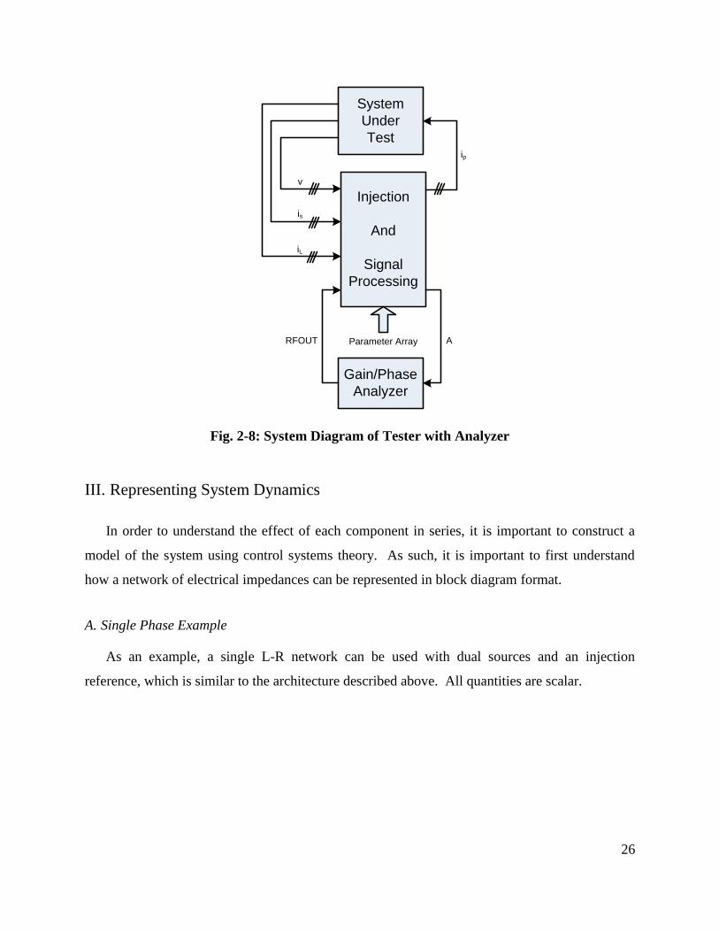
Fig. 2-8: System Diagram of Tester with Analyzer
III. Representing System Dynamics
In order to understand the effect of each component in series, it is important to construct a
model of the system using control systems theory. As such, it is important to first understand
how a network of electrical impedances can be represented in block diagram format.
A. Single Phase Example
As an example, a single L-R network can be used with dual sources and an injection
reference, which is similar to the architecture described above. All quantities are scalar.
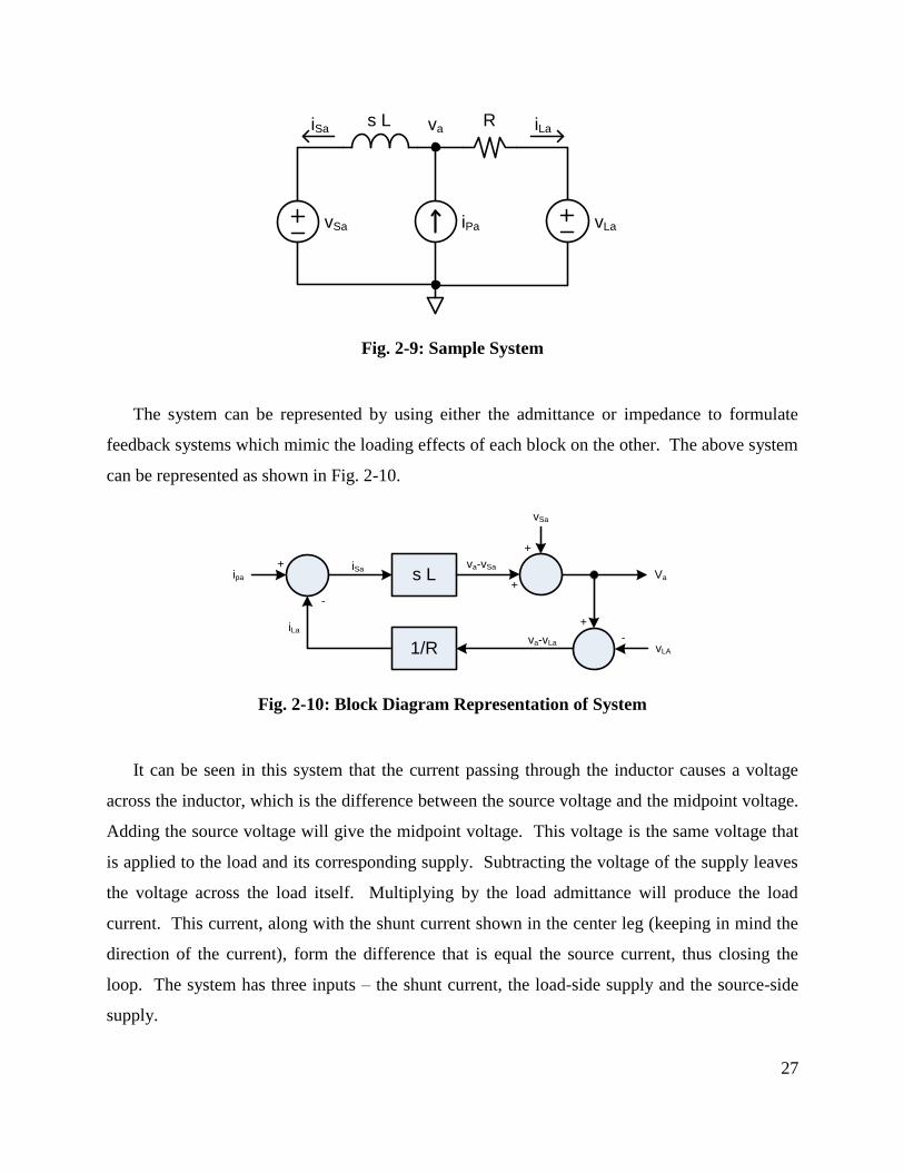
27
s L R
vLavSa iPa
iLaiSa va
Fig. 2-9: Sample System
The system can be represented by using either the admittance or impedance to formulate
feedback systems which mimic the loading effects of each block on the other. The above system
can be represented as shown in Fig. 2-10.
s L
1/R
Va
vLA
ipa
iSa
iLa
va-vLa
va-vSa
vSa
+
+
+
+
-
-
Fig. 2-10: Block Diagram Representation of System
It can be seen in this system that the current passing through the inductor causes a voltage
across the inductor, which is the difference between the source voltage and the midpoint voltage.
Adding the source voltage will give the midpoint voltage. This voltage is the same voltage that
is applied to the load and its corresponding supply. Subtracting the voltage of the supply leaves
the voltage across the load itself. Multiplying by the load admittance will produce the load
current. This current, along with the shunt current shown in the center leg (keeping in mind the
direction of the current), form the difference that is equal the source current, thus closing the
loop. The system has three inputs – the shunt current, the load-side supply and the source-side
supply.

28
It can be demonstrated that this is valid, and the block diagram may be manipulated by
removing some of the sources to reconstruct familiar situations. Removing the source and load
gives the diagram shown in Fig. 2-11.
s L R
vSa iPa
iLaiSa va
Fig. 2-11: Sample impedance with shunt current and load side supply removed
To calculate Va, one may simply use a voltage divider, immediately providing R/(R+s L)
Vsa as the voltage at V. Using feedback diagrams and removing unnecessary elements, one may
use the block diagram to get the same result shown in Fig. 2-12. The diagram on the left is
produced by removing the unused inputs and replacing the summing junction with an inverting
gain, as the second input of the junction was not used. The diagram can be simplified to that
shown on the right-hand side of the diagram.
s L
1/R
Va
iSa
iLa
va-vSa
vSa
+
+
-1
s L/R
VavSa
+
-
Fig. 2-12: Block diagram of example with perturbation and load side supply removed.
Applying the feedback formula will produce the correct output:
(24)

29
Any variable may be selected as the output of interest. A similar manipulation will provide the
current as:
(25)
which one may immediately recognize as the conductance of the circuit. One may repeat this for
the other two sources. A particular example of interest, as will be seen later, is the shunt current,
shown in Fig. 2-13.
s L R
vLavSa iPa
iLaiSa va
Fig. 2-13: Injecting Shunt Current Into Example
The block diagram can be simplified to the following by removing the unused inputs:
VaiPa
+
-
s L
1/RiLa
iSa
Fig. 2-14: Simplified Block Diagram Representing Shunt Injection into Example
The voltage may be found via the feedback formula:
(26)
which can be seen as the parallel impedance of the source and load.

30
If one were to use the response of and also repeat for , one could divide these two
responses to get impedance . However, if either R or L were set very small, the corresponding
response on would be very small, which may introduce practical challenges associated with
measuring such a small response to perform this calculation.
B. Application to Three-Phase D-Q Systems
Applying this to a three-phase D-Q system, one may represent the systems described by Fig.
2-2 with the following block diagram.
ZS
YL
v
vL
ipiS
iLv-vL
v-vS
vS
+
+
+
+
-
-
Fig. 2-15: Block Diagram Representation of System Under Test
In this diagram all lines have been vectorized, and all variables are a vector of size 2. and
are both 2x2 matrices of transfer functions. While this is not the finalized block diagram of
our system, it provides a basis on which one can develop a model of the measurement and
injection system.
Injecting current into the system via , one can get the transfer function to the corresponding
change at the point of common coupling between the two systems and the injection:
(27)
One may similarly obtain the load current:
(28)
One may use this information as described earlier to solve for or the source
impedance . This diagram will be used in the future to build sensors and other elements into
the model.
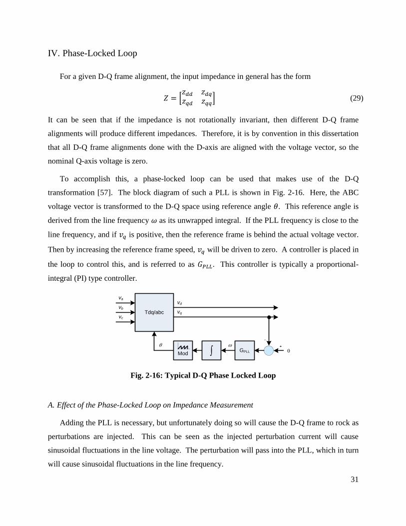
31
IV. Phase-Locked Loop
For a given D-Q frame alignment, the input impedance in general has the form
(29)
It can be seen that if the impedance is not rotationally invariant, then different D-Q frame
alignments will produce different impedances. Therefore, it is by convention in this dissertation
that all D-Q frame alignments done with the D-axis are aligned with the voltage vector, so the
nominal Q-axis voltage is zero.
To accomplish this, a phase-locked loop can be used that makes use of the D-Q
transformation [57]. The block diagram of such a PLL is shown in Fig. 2-16. Here, the ABC
voltage vector is transformed to the D-Q space using reference angle . This reference angle is
derived from the line frequency as its unwrapped integral. If the PLL frequency is close to the
line frequency, and if is positive, then the reference frame is behind the actual voltage vector.
Then by increasing the reference frame speed, will be driven to zero. A controller is placed in
the loop to control this, and is referred to as . This controller is typically a proportional-
integral (PI) type controller.
Tdq/abc
ModGPLL∫
vd
vq
va
vb
vc
q w0
-
+
Fig. 2-16: Typical D-Q Phase Locked Loop
A. Effect of the Phase-Locked Loop on Impedance Measurement
Adding the PLL is necessary, but unfortunately doing so will cause the D-Q frame to rock as
perturbations are injected. This can be seen as the injected perturbation current will cause
sinusoidal fluctuations in the line voltage. The perturbation will pass into the PLL, which in turn
will cause sinusoidal fluctuations in the line frequency.
32
B. Locking the PLL
Signal content that is not at the fundamental frequency will have effects on the angular
frequency of the PLL. When measuring the impedance, it is assumed the D-Q frame is at
constant frequency. If the PLL were allowed to keep changing the line frequency, this
assumption would not be valid.
Alternatively, locking the PLL during a sweep may work in theory if the estimated line
frequency were exactly the same as the actual line frequency. Since there will always be some
error in the estimated and actual frequencies, locking the PLL would allow the D-Q frame to
escape at a relative speed equal to the estimation error. Thus the measurement would not be
synchronized with the voltage vector once the PLL is locked. For example, if the actual line
frequency is 400 Hz, and the PLL is completely disabled when the frequency is 399 Hz, the
voltage vector will rotate on the D-Q plane at 1 Hz, removing the steady-state operating point.
As a resolution, the PLL bandwidth can be reduced to be significantly below the lowest
perturbation frequency, ensuring that there will be no noticeable effect on the PLL by the
perturbation. As the PLL is still running, small errors between the PLL estimated frequency and
the actual frequency can be compensated without rocking the frame. Using PI control, one may
write the equations as follows:
(30)
In this form, one cannot change the gains instantaneously. Simply moving the gain through the
integral term, however, allows for sudden changes in the value of :
(31)
Upon achieving a lock on the voltage, will be very small. It is therefore possible to make step
changes in and without making a significant step change in . Thus the gain of the PLL
can be changed on the fly by implementing (31) instead of (30), although for constants and
, these two equations are equivalent.

33
C. Phase Locked Loop Accuracy and Imbalances
While the ideal voltage vector is sinusoidal with all three voltage vectors equal in magnitude,
as described in (1); in practice, the three voltage vectors are not going to be equal. The resulting
imbalances will make the steady-state voltage vector oscillate at a frequency of [57]. We can
see that this is possible by considering the fact that an imbalance in voltage produces a positive
and a negative sequence component. The zero sequence component does not transfer to the D-Q
frame, and is normal to it. The D-Q frame rotates with the voltage vector. The negative
sequence rotates in the opposite direction of the D-Q frame at the same line frequency. Thus,
from the D-Q frame, it would appear that the negative sequence is rotating at twice the line
frequency in the opposite direction.
Depending on the amount of imbalance in the line voltages, the oscillations may be
significant enough to affect the phase-locked loop. To mitigate this, a phase-locked loop may be
used that isolates the positive sequence of the voltage, such as the one used in [58].
Such a PLL makes use of two rotating reference frames. The dynamics between the two
reference frames are decoupled via a state-space system, providing as its output four variables:
, , , and . Although the reference frame used in [58] is more general and can
eliminate any harmonic, it can be simplified to operate only with the positive and negative
sequences, simplifying its implementation. The only variable under control is the positive
sequence Q-axis voltage, as shown in Fig. 2-17.
ModGPLL∫
va
vb
vc
q w-
+
vd+
vq+
vq-
vd-
0
Dual -
decoupled
Synchronous
reference
frame
transformation
Fig. 2-17: Dual Decoupled Synchronous Reference Frame based PLL

34
V. Summary
We have constructed a block diagram with unidirectional signal flow which represents the
system under test. It was shown from this block diagram how one may calculate the current
entering the load, as well as the voltage response from a current injection, which will be useful
for determining the magnitude of the responses obtained from injection.
An algorithm has been developed that allows for multiple shunt current injections between
the load and source subsystems to identify the input impedance of the load or the output
impedance of the source of a three-phase AC network in the D-Q domain.
We‟ve discussed the use of a phase-locked loop to synchronize the reference frame of the
instrument with the rotating voltage vector that is measured. The PLL chosen mitigates the
effect of unbalance in the system. It was shown that the PLL has to be present and operational
during the sweep, but should be reduced to a low bandwidth prior to measurement to ensure the
PLL frequency is not disturbed by the injected perturbation during the measurement process.

35
Chapter 3. Hardware Implementation Architecture
This chapter discusses the hardware architecture and factors to consider when constructing
the actual measurement system. Several aspects of the design–ranging from the power stage, to
the analog processing, to the digital processing–will be considered. The solution will be derived
from a set of requirements specified a priori. Factors found during implementation will be
discussed, identifying both the recommended and required features of the specified architecture
and its components.
I. System Architecture
The design of the system architecture can be posed as a recursive problem, where the
problem can be broken up into several subsystems which implement key functions. These
subsystems are partitioned to isolate functionality, improve debugging and reduce development
cycle time, and improve component re-use. As defined in Chapter 2, the key hardware
requirements can be summarized as follows:
1. The system must be able to inject a specified waveform used as a perturbation into the
system during its operation.
2. The system must be able to measure the resulting currents and voltages produced by the
system under test.
3. The system must be able to apply the required transformations.
4. The system must be able to output a second set of signals in the rotating domain.
5. The system must interact with the user, who configures the system parameters and
coordinates the measurement.
6. The system must be able to present the results back to the user.
7. The system must be able to coordinate the measurement process.
The system should do these with the following desired characteristics:
1. Minimal noise

36
2. Maximal bandwidth
3. Minimal error
4. Maximum repeatability (accuracy)
The non-deal characteristics of the components used to implement the solution will influence the
measured results. These non-idealities are some of the key elements which differentiate an
actual implementation from a simple simulation, and thus ultimately limit the measurement
instrument‟s capabilities.
The choice of the subsystem boundaries are also strongly influenced by the available
technologies used to implement the system. The following are chosen as the subsystems. The
subsystem boundaries are chosen also as a way to abstract the power level from the other
modules:
Power Processing Subsystem
Signal Conditioning Subsystem (analog + digital)
(Supervisory) Control and HMI
II. Overview of System
The hardware for the impedance tester consists of a PC controlling a network analyzer and a
universal controller (DSP-based digital controller). The controller in turn was connected to a
specialized analog interface specifically designed for this application. The analog interface
provided three analog references to three current amplifiers, which were transformer-coupled to
the power system. Sensors were placed to measure the current and voltage responses as well as
the fundamental, and the sensor responses were sent back to the specialized analog processing
board. The entire system uses isolated power supplies on each sensor and interface to prevent
ground loops and minimize the measurement noise which can be created from such loops [59].
A conceptual block diagram showing the system is provided for reference in Fig. 3-1.

37
Fig. 3-1: System Block Diagram
III. Subsystem Key Functions and Interfaces Overview
The subsystems are chosen to meet the functional requirements of the application. The three
subsystems are configured as shown in Fig. 3-2.

38
1
2
3
Power Processing Subsystem
Signal Processing Subsystem
Control Subsystem
Fig. 3-2: Subsystem Definitions
A. Power Processing Subsystem
The power processing subsystem is responsible for managing the power as related to the
application. Injection equipment and sensors appear at the boundary between this subsystem and
the signal-conditioning subsystem. Existing equipment may be used, swapping out the power
processing subsystem for a different one to adapt the measurement unit to a different subsystem,
leading to a scalable (power level can be adjusted), modular and flexible (can be developed in
parallel) architecture.
The power processing subsystem has two interfaces. The first is the power ports used to
connect the test unit to the system under test (Interface 2 in Fig. 3-2). The second is the

39
measured currents and voltages from the transducers, and the reference current outputs (Interface
1 in Fig. 3-2).
B. Signal-Conditioning Subsystem
The signal-conditioning subsystem attempts to provide ideal analog inputs and outputs,
eliminating noise and preparing the signals for digital sampling. Furthermore, it is responsible
for synchronizing the transformation with the voltage, performing the transformation, providing
the perturbation references and identifying the actual transfer functions. Included in this
subsystem is the gain / phase analyzer used to identify the transfer function via a frequency
sweep. This subsystem consists of both analog and digital processing hardware.
This subsystem has two major interfaces. The first is the interface to the power processing
subsystem, which provides the reference perturbation currents and reads the measured currents
and voltages to the power stage. This interface is an analog interface. The second major
interface is that which communicates with the control component. This component can be
considered to be composed of two pieces. One is the DQ transformation control, and the other is
the control that acquires the transfer function. Both are digital.
C. Control and HMI subsystem
The control and HMI subsystem is responsible for coordinating the major actions needed to
acquire the impedance, which consists of instructing sweeps to be performed, and configuring
the signal-processing subsystem. The user controls the parameters of the sweep via this module,
which is also used to present the results to the user. For the purposes of this implementation, this
module is implemented as a PC.
This module has two major interfaces, one being the results interface which is presented via a
text and graphical front end to the user, and the second is the interface which controls the signal
processing unit.

40
IV. Power Processing Subsystem – Injection
The power processing subsystem has two major functions. Firstly, it is responsible for
injecting the perturbation into the system. Secondly, it is responsible for measuring the resulting
changes in the currents and voltages at the interface where the impedance is to be acquired. The
subsystem is shown in Fig. 3-3.
1
2
Fig. 3-3: Power Processing Subsystem Showing Interfaces 1 and 2
The system under test shown in Fig. 2-8 has as its input three current sources. It is necessary
to construct a mechanism to inject these three currents in order to cause a perturbation in the
system. It is also necessary to find a way to bring back the voltages and currents to a processing
mechanism so that the resultant ABC domain data can be transformed to the D-Q domain.
As outlined in Chapter 1, several attempts have been made to create this perturbation source,
although in those implementations, they were modulating impedances and using voltages which
in turn caused currents, and did not actively control the current. The approach taken here uses
three linear amplifiers operating in current mode. These amplifiers are isolated from the main
power system via transformers. The input to the amplifiers is a signal ipxref where x is a, b, or c.
The output of the amplifiers is the injected current into the system. Each phase has a
configuration as shown in Fig. 3-4.

41
ipxref
ipa
Fig. 3-4: Injection Reference to Injection Current
V. Power Processing Subsystem – Measurement
The same system has as outputs three sets of measurements. These measurements are
implemented via sensors. The sensors measure the line-to-neutral voltage, and the line current in
the ABC domain. Sensors need to measure the full line current and voltage and translate the
levels down to that which can be converted to a signal for use in digital processing. Additional
requirements regarding isolation and high bandwidth, while having a guaranteed maximum and
minimum signal level, make hall-effect current and voltage sensors a desirable solution.
A challenge in sensor design involves the requirement of the sensor to measure the full
stationary frame measurement variables, even though all we are interested in is the small
perturbation on top of it. Thus the sensors must have a large range, most of which will not be
used for small-signal processing. Thus it is important to use as much of the dynamic range as
possible for each sensor. Furthermore, based on the impedance ratio between the source and the
load, the majority of the perturbation may flow in the opposite direction to the current which is
being measured, producing an even smaller response. It is therefore important to choose good
sensors.
A. Current Sensors
i) Sensor Selection
Many kinds of current sensors are available and in development for use in power
applications, such as those mentioned in the overview provided in [60]. Examples of current
sensors that may be used are:
Resistive current shunts
Hall effect current sensors
42
Current transformers
Rogowski Coils
Giant Magnetorestrictive effect sensors (GMR)
Giant Magnetoimpedance effect sensors (GMI)
The selection of a current sensor for use in three phase impedance measurement systems
should be done according to a set of performance requirements related to the application and the
required bandwidth. In determining a sensor‟s bandwidth it is important to know how much
phase shift the sensor will provide at high frequencies. This phase shift will distort the
measurements at higher frequencies if it is not compensated. Added phase delay from the
current sensors will make the impedance increase as the algorithms divide by the current
response matrix, turning phase delay into phase gain.
While some current sensors have high bandwidth, they may not be able to reliably measure
low-bandwidth signals. Impedance measurement requires accurate measurement of high and low
bandwidth signals. Sensor technologies such as Rogowski sensors and hall-effect transformers
may not have low enough bandwidth to reliably get measurements at very low frequencies. New
hybrid technologies are emerging that may eliminate this restriction.
Furthermore, there is a challenge associated with integration of the current sensor for
measurement applications into the actual system. There is a fundamental limitation related to
accuracy and resolution. The current sensor must be able to measure the full line current of the
application. However, only the current related to the perturbation is of interest, which is very
small compared to the fundamental current. Therefore, only a small part of the total dynamic
range is of use for impedance measurement.
ii) Chosen Sensors
The current sensors chosen are LEM sensors with part number HTA-300. The sensors have a
150 kHz bandwidth, as indicated by the data sheet. The sensors connect to an interface PCB that
provides each sensor its own isolated power source to prevent ground loops in the measurement
circuit. The sensors and the associated interface PCB are shown below.

43
Fig. 3-5: Current Sensors
The sensor response can be modeled by a first-order response, and the corresponding frequency
response is shown in Fig. 3-6.
Fig. 3-6: Current Sensor Frequency Response (Negative reference)
-24
-23
-22
-21
-20
Magnitu
de (
dB
)
101
102
103
104
105
-182
-181
-180
-179
-178
-177
Phase (
deg)
Bode Diagram
Frequency (Hz)

44
B. Voltage Sensors
i) Sensor Selection
Almost every voltage sensor available from LEM has a very low bandwidth, and thus was
unsuitable to be used for measuring impedance characteristics at high frequencies. Furthermore,
when the line frequency is increased, it becomes more restricted, as the DQ transform will take
components from higher frequencies. The original attempts to measure impedance were
performed with available equipment, using a LV-1200-SP1 sensor. The bandwidth of this sensor
was 8 kHz, and thus it limited the frequency range of the measurements. Subsequent evaluation
of available LEM sensors indicated that the phase delay at the bandwidth was significant, and
may be approximated by a first-order model. Phase delay in the voltage sensors will affect the
phase delay of the computed impedance. Phase delay in the voltage sensors will cause the phase
of the measured impedance to decrease. The first sensor chosen is shown below.
Fig. 3-7: Original Voltage Sensor
After measuring its transfer function, the sensor is found to be insufficient, as the bandwidth
is too low. The measured bandwidth is shown in Fig. 3-8.
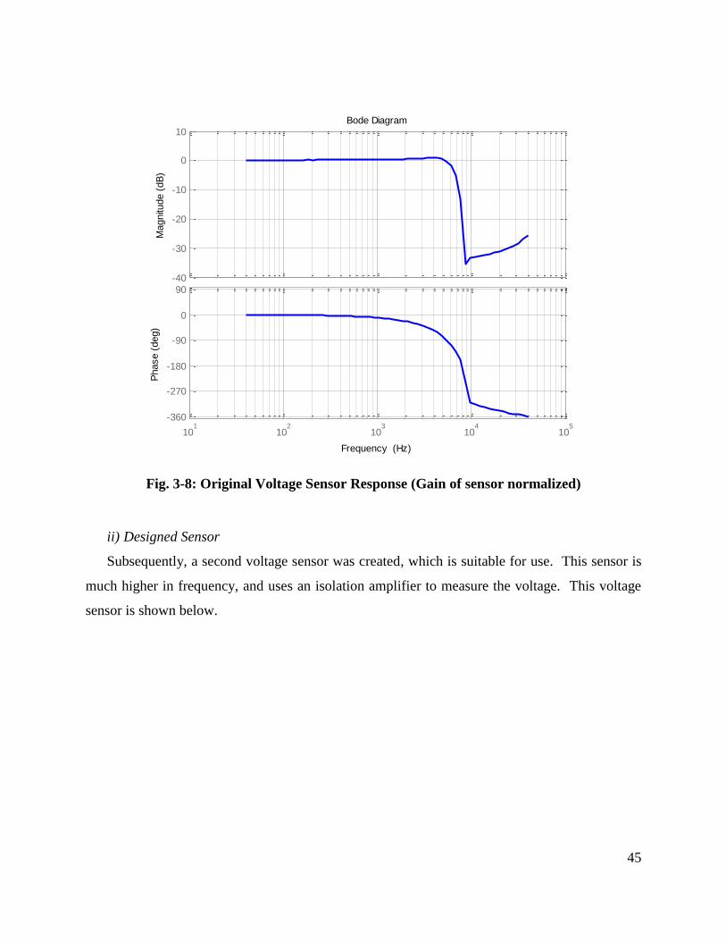
45
Fig. 3-8: Original Voltage Sensor Response (Gain of sensor normalized)
ii) Designed Sensor
Subsequently, a second voltage sensor was created, which is suitable for use. This sensor is
much higher in frequency, and uses an isolation amplifier to measure the voltage. This voltage
sensor is shown below.
-40
-30
-20
-10
0
10
Magnitu
de (
dB
)
101
102
103
104
105
-360
-270
-180
-90
0
90
Phase (
deg)
Bode Diagram
Frequency (Hz)

46
Fig. 3-9: New Custom Voltage Sensors
The sensor consists of a voltage divider with a 1:51 ratio. The maximum input voltage of the
sensor is 500 volts. To increase performance, the resistive divider uses low inductance resistors
with values of 10 kilo-Ohms and 200 Ohms, reducing the effect of noise at the sensors output.
The resistive divider feeds an instrumentation amplifier with input protection, which accurately
measures the small voltage from the sensors. The amplifier then feeds an analog device AD215
isolation amplifier, which isolates the measurement signal from the power line. It is
recommended that when connecting this sensor, you connect the negative input of the sensor to
the neutral conductor. The AD215 provides a separate fly-back power supply that is capable of
driving the instrumentation amplifier. As the output signal from the AD215 is going to the
measurement system, an isolating DC/DC converter is used that isolates the input power from
the measurement system, similar to that of the current sensor. The sensor produces an output
voltage ranging from +10 volts to -10 volts.
The sensors developed have the following measured transfer function from input to output, as
measured with an amplifier and two differential probes:

47
Fig. 3-10: Voltage Sensor Transfer Function vs Tektronix Probe
The isolation amplifier has a 2 microsecond transport delay. It is seen here that the delay
matches closely the phase characteristic of the sensor. The resultant transfer function is shown in
(32):
(32)
This will be the model of the voltage sensor that will be used to determine the sensor
characteristics in the DQ domain.
-0.6
-0.4
-0.2
0
0.2
Magnitu
de (
dB
)
101
102
103
104
105
-30
0
Phase (
deg)
Sensor Transfer function vs Tektronix P5205 Differential Probe
Frequency (Hz)
Phase A
Phase B
Phase C
2 s Delay

48
VI. Cabinet
The cabinet containing the impedance measurement equipment is shown in Fig. 3-11. This
cabinet contains all of the power-processing equipment and the digital controller used to
coordinate the injection. Care must be taken to ensure that there is sufficient air flow across the
three gaps in the cabinet. Lack of airflow will cause the amplifier to shut down due to thermal
overload, and thus may require an external fan. For the purposes of this implementation, a box
fan sufficed, and was placed in front of the cabinet at the height of the middle amplifier to
substitute for commercial rack-mounted fans, which could have been used instead.

49
Fig. 3-11: Injection Hardware Cabinet
The lower workings of the cabinet contain the transformers, contactors, and sensors used
during measurement. It should be noted that the injection lines enter the system between the two
sets of current sensors and couple at the load side terminal block. The main conductors can be
seen traversing the bottom of the cabinet from the load side terminal block to the source side
terminal block. The conductors are 150 square millimeters (250 kcmil) and are made of copper
conductor.

50
Fig. 3-12: Injection Hardware Cabinet Lower Stage
VII. Signal-Processing Subsystem
The signal-processing subsystem consists of an analog section that conditions the signals for
analog sampling, and a digital signal section that processes the signals and coordinates timing
and sampling. Within this subsystem there is also an analog-digital interface which is of
particular interest. This interface will determine which sampling and resolution issues will add
non-ideal behavior to the system in the form of noise, and which may thus be a bottleneck for
bandwidth.

51
1
3
Fig. 3-13: Signal Processing Subsystem
A. – Digital Subsystem - Universal Controller
In order to choose a digital control system, an analysis of IO is required. Many possibilities
can be chosen to implement the digital control system, and while this is not the focus of this
dissertation, the digital control system choices significantly affect the capabilities that can be
provided by the instrument, most significantly the processing bandwidth. Here, many signals
must be simultaneously sampled, including all currents and all voltages.
When considering the digital controller, one must consider the interfaces required to interact
with the system. The digital interfaces which are required in this and all measurement systems

52
following the recommended architecture can be seen as the boundaries of the colored box in Fig.
3-1. The selection of conversion devices have a notable tradeoff between bandwidth and IO
when using a serial bus compared to a parallel bus; however, the number of required IO channels
prevents us from using a purely parallel implementation. Furthermore, the effect can be reduced
if the serial data can be read in parallel to a new conversion.
The universal controller is the current digital control platform implemented at CPES. The
controller is an field-programmable gate array (FPGA)-centric design with a DSP. Many
available references discuss the controller [61-65], and its schematics are available at [61]. The
controller was developed at CPES, and since its inception more than 28 controllers have been
manufactured with applications ranging from embedded motor controllers [66] to distributed
converter control systems [67], and from communication protocol research to hardware-in-the-
loop test setups [62, 65] which integrate the controller with a simulation engine. The block
diagram of the controller is shown in Fig. 3-14.
Fig. 3-14: Universal Controller Functional Block Diagram
In this controller, the FPGA organizes the functions on the board, but the DSP creates the
requests, as the user‟s application control code usually resides within the DSP. The controller
itself is shown in Fig. 3-15.

53
Fig. 3-15: Universal Controller
B. Digital Subsystem – Control System Communication – Hardware and Physical Interface
The interface between the control subsystem and the signal processing subsystem does not
have to be fast and has no hard real-time requirements. Most communication solutions are
therefore applicable. Here, potential solutions include, but are not limited to:
Ethernet
Serial Bus
GPIB
USB
Shared Memory
The primary requirement of this interface is the ability to read and write memory to set states.
Based on this architecture, no interrupt capability is necessary. This is because the variables
being controlled are part of the digital subsystem and are used to route signals; and because there
are set parameters for the PI PLL, and thus there is no need for synchronism based on the
parameters being modified. For convenienc,e this system may be chosen to be a prepackaged
Peripheral
Expansion
Multiprocessor
Connector User DIP
Switches Hex
Display
Multiprocessor
Connector DSP Flash
Expansion
Connector I/O
FPGA DSP
PCI
Dual-Port
Peripheral
EEPROM
DAC
Communication
Transceivers
Expansion
Connector I/O

54
solution that is either a built-in feature of the digital signal processor selected or a function
provided by an auxiliary chip. It is critical, however, that the requirements of the solution
chosen do not interfere with the ability of the real time tasks required to perform the
transformation.
i) Implementation
The analog measurement subsystem is sensitive to noise. It is important to ensure that there
are no large ground loops, including loops involving the PC through communication cables.
Techniques used to mitigate noise coupling are strongly recommended and may be found in
resources such as [59]. The voltage transients on the universal serial bus are fast and add noise
to the system. The universal serial bus section of the PCB should therefore be isolated from the
main PCB.
In the hardware built for this study, this isolation was accomplished via digital isolating chips
(Analog Devices ADUM1100). These chips allow the USB interface to operate on a separate
ground plane. Separate power is provided to this isolated circuit via an isolated 3.3 volt output
DC/DC converter. The ground of the USB connector is shared with this plane, and this isolation
separates any grounding issue that connecting the USB cable to the PC may provide.
The universal serial bus interface chip chosen is the MAX3420E. This chip directly connects
to the USB data lines via a series 33 Ohm resistor. The chip also accepts a 3.3 volt signal that
connects to the USB power pin on the connector. This pin is used to determine if the USB cable
is plugged into the port. As this device is used as a slave, a type B connector is present on the
PCB for connecting the USB cable. The USB chip also requires either a silicon oscillator or a
crystal. A crystal was chosen, and this also connects to the chip to provide a clock to the USB
onboard circuitry.
The schematic of the USB interface is shown in Fig. 3-16. The green area of the schematic is
galvanically isolated from the main ground, and is also the ground shared with the USB cable.
The grey area is the input power ground. Two linear regulators can be seen in the upper right
hand corner. These power the digital isolating buffers (shown crossing the ground planes
between green and white) with 3.3 volts.

55
SCLKR
SCLK
MISO
SS_L
MOSI
RST_L
GPX
INT
MAX3420E
USB
Interface
DC DC
Pin3.3 V
3.3V
Linear
Regulator
DX+
DX-
VSENSE
General Purpose
I/O Header
Iso
latio
n
Ba
rrie
r
Fig. 3-16: USB Interface Schematic

56
C. Analog Subsystem Overview
The analog interface will ideally take an input signal and provide an ideal electrical signal
which can be sampled by the analog-to-digital converter without ill effects. Similarly, it will
provide an ideal isolated output signal which can be provided as a reference to an injection
source. The parameters considered here in making this decision are:
Signal bandwidth
Signal dynamic range
Signal isolation requirements
Signal EMI
D. Analog Subsystem Architecture
With the exception of two onboard DA converters, the universal controller is a completely
digital platform. To interface with the rest of the system, we created an analog interface. The
interface contains:
18 Analog input channels (via SMB coaxial connectors)
6 Analog output channels (via SMB coaxial connectors)
1 USB interface (via a USB type B connector)
1 Power input (via screw terminals)
1 Controller interface (via a 60 pin 2x30 header)
The PCB is shown in Fig. 3-17 below, with the universal controller mounted on top of it.

57
Fig. 3-17: Analog and USB Interface with Universal Controller Mounted On Top
The PCB is an 8-layer PCB with more than 5000 pads, and is 0.110 inches thick. To
minimize cross-talk, a ground trace separates any two conductors, including digital conductors,
as their frequency is very high. A block diagram of the PCB is shown below.

58
Fig. 3-18: Analog Measurement PCB Architecture (Excluding USB Interface)
The PCB consists of three sets of six-channel AD converters, and six individual digital-to-
analog converters. All converters communicate with the controller via a serial peripheral bus.
As the connections directly interface the FPGA on the digital controller, there is digital interface
protection consisting of a transient voltage suppressor and a current limiting resistor on all lines
going to the universal controller connector. In the event of a failure on this PCB, high voltage
will be prevented from traveling to the universal controller FPGA, protecting it in such an event.
E. Analog Subsystem Inputs
i) Implementation
The analog inputs are converted to a digital signal by an Analog Devices AD7656 analog-to-
digital converter [68]. This converter has a maximum sample rate of 256 kilosamples per
second. Each channel samples simultaneously, and each channel is converted individually with
its own dedicated successive approximation register-based state machine.

59
The input stage of all analog channels is driven by a high-impedance instrumentation
amplifier with a high common-mode rejection ratio. The AD7656 is driven by a dedicated line
driver preceded by a sixth-order Chebyschev filter, which is in turn preceded by a common mode
choke.
The corner of the Chebyschev filter is at 20 kHz, and the converter attempts to eliminate all
signal content with a very sharp roll-off to prevent anti-aliasing. As such, each channel will
produce a large phase delay. However, since all channels will produce a nearly identical phase
delay, the effect of the delay is mitigated.
It should be noted that the op-amp chosen has a quiescent current of 10 milliamps, which,
although seemingly small at first, will provide significant power consumption when supplied
from +/- 15 volts. There are 18 input channels, with each channel containing 4 op-amps.
Consequently, the PCB will require significant cooling to keep the PCB from overheating, as
there are a total of 72 op-amps in the signal conditioning path, each consuming 300 milliwatts of
power, providing a total of 21 watts of power dissipation.
F. Analog Subsystem Outputs
i) Function
The analog output subsystem accepts digital results from the algorithm implemented in the
FPGA, and makes the results available to analog inputs on the instrumentation. There are two
sets of analog outputs which one may consider groups. The first group is the outputs that go to
the gain and phase analyzer. The second group is the outputs that go to the amplifiers. The
output stage consists of the digital-to-analog (DA) converter followed by analog filtering.
Additional requirements demand the outputs be isolated. Finally the analog output subsystem
must have the ability to drive the signal. At the output of the filter is a line driver, which is used
to connect to the cable that is used to pass the analog signal from the analog interface PCB to its
recipient; either the analyzer or an amplifier.
ii) Signal Conditioning and Isolation
As the network analyzer is sensitive to noise, it is important to ensure that the outputs are
clean. Isolation amplifiers can be used to eliminate ground loops. A second option is to use
isolation on the digital side, before the DA converter. If this is done, there must be very stable

60
supplies available for the DA on the isolated plane, as well as separate digital and analog
grounding planes present to prevent digital noise from corrupting the analog signal [59].
Different kinds of isolation amplifiers can be implemented, ranging from optical isolation
amplifiers to capacitive isolation amplifiers to inductive isolation amplifiers. Of the amplifiers
commercially available, the inductive ones seem to have the highest bandwidth. Additional
issues with isolation amplifiers are their common-mode rejection ratio (CMRR). If the CMRR is
not high, then the effect of the isolation is mitigated. Generally the CMRR decreases with the
frequency, as capacitive effects grow between the input and output.
Each analog output is isolated via the use of an Analog Devices AD215 isolation amplifier.
This isolation amplifier has a bandwidth of 250 kHz, and can be conceptualized as a chopper and
a reconstruction circuit. As this amplifier is typically used on the input side of a system, the
amplifier takes its power from the output side, and thus an isolated DC/DC converter is required
for each amplifier providing +/- 15 volts to allow us to use this chip for output isolation.
iii) Digital-to-Analog Conversion
The digital-to-analog converter (DAC) chosen is a Texas Instruments DAC8831. The DAC
works with an external amplifier. The Texas Instruments OPA602 was chosen for this. The
DAC connects to both the positive and negative input terminals of the op-amp as well as its
input, and uses these to produce the desired output voltage at the output of the op-amp. The
structure of the DAC is a resistive ladder divider. The DAC and high-performance amplifier
drive the isolation amplifier, which in turn drives a line driver on the isolated side.
iv) Implemented Solution
The structure of the analog output channel is shown in Fig. 3-19 below. Not shown are the
high-impedance pull-up and pull-down resistors to keep the converter in a stable state if powered
without the presence of the universal controller.

61
R
Bandgap
reference
DAC
Fig. 3-19: Analog Output Stage Schematic
It should be noted that noise on this circuit will couple to the output, and as such, sufficient
filtering using multi-layer ceramic chip capacitors is specified at several capacitance ranges to
mitigate the effect of such noise. The DAC is a 16-bit device, and with an output range of +/- 10
volts, the least significant bit (LSB) represents a voltage magnitude of 305 microvolts.
VIII. Control Subsystem
The control subsystem is implemented primarily in a PC. However, due to the interface
restrictions of the selected instrument in the DQ domain, a GPIB converter must be added to this
subsystem. This is the most abstract and flexible subsystem of three subsystems. The
implementation is in Matlab. This subsystem has no hard real-time requirements, and thus any
number of platforms can be chosen to implement it.
IX. Summary and Conclusions
The hardware for our system was constructed to implement the impedance tester. The
hardware consisted of linear power amplifiers to inject the three perturbation currents into the

62
system. The injection amplifiers were coupled to the system via a transformer due to limitations
on its isolation and voltage range.
We developed sensors to measure the voltages at the point of common coupling between the
two subsystems and the injection unit. Existing voltage sensors were insufficient as they
provided significant phase delay at high frequencies and had low bandwidth; therefore, we
created our own voltage sensors. The new sensors provided a much lower phase shift.
The current sensors chosen are for the full line current. When measuring smaller systems,
we found that increasing the current sensor gain will improve measurement results, giving rise to
a new set of current sensors with higher gain; although at the same time, a higher impedance
added into the circuit.
A signal-processing and mixed signal technology PCB was implemented to acquire all sensor
signals and provide them to the standard control processing platform developed at CPES prior to
this project. This PCB also included an isolated section providing USB communication
capability to the control platform. The PCB is an 8-layer PCB containing more than 5000 pads.
A PC was used to run Matlab and coordinate the activities of the hardware via software-
based supervisory control and data acquisition, and made use of both USB and GPIB to
communicate with the instrumentation.
A gain/phase analyzer from Agilent Technologies was integrated into the system providing
the frequency response measurement function to the system architecture. Input and output
signals from this analyzer were passed directly to the developed signal-processing PCB, which in
turn was processed by the DSP.

63
Chapter 4. Software Implementation Architecture
I. Overview
Like the software, the hardware can be designed in a modular fashion. The hardware
presented in the previous chapter is controlled via a set of software programs running on multiple
platforms, from a graphical user interface presenting results to the user via scripting language in
a host program, which makes calls to Windows running on a PC; down to a low-level language
describing the interconnection of registers and combinational logic implemented in an FPGA
found in the signal-processing subsystem.
The software used to control the system is written in a hierarchical fashion. Higher-level
software is used to implement the measurement algorithm and acquire individual sets of
frequency response data from the instrumentation. Matlab is chosen as the language to
implement this software due to its computational proficiency and capability to display graphical
results. After such data is acquired, Matlab is also used to acquire the impedance. Lower levels
of software assist in accomplishing this task.
The lower-level software was written so it could be incrementally tested and verified.
Modularity and flexible software design practices were used in designing this software. The
design approach taken was to specify the interfaces and functions of each component and how
each component interacted with the other components. Individual components can then be
aggregated to form the final software solution.
The modules were assigned based on functional partitioning of the application. Interfaces
result from drawing boundaries across the system to isolate and contain functionality into
modules. These boundaries are chosen based on several criteria:
If the function must run in real-time or can be post-processed
The ease of changing and debugging the function
The application-independent nature of the function

64
Matlab must communicate with the instrumentation, the DSP, and the user. The functionality
associated with communication can be encapsulated in to modules which are application-
independent. Since there is no available existing mechanism in place to do this directly in an
efficient manner, Active-X controls are developed that encapsulate the overhead of interfacing
with the instrumentation and the DSP. As communication with the DSP occurs over a
completely custom interface defined by this application, the Active-X control that interfaces with
the UC encapsulates the overhead associated with forming packets and acquiring the USB device
from the system, leaving only functional objective-based actions to Matlab, while hiding the
details of the communication implementation.
Secondly, the DSP executes code to control the injection, as well as to communicate with the
Active-X component just described. Matlab provides the control of the DSP states and signal
outputs to the analog subsystem, and the injection is calculated in an interrupt-based subroutine
executing at a fixed frequency. The parameters sent from the Active-X over USB are managed
in an interruptible message loop that runs whenever the interrupt is not running. This
architecture is depicted in Fig. 4-1.

65
PC
Matlab
IDispatch IDispatch
GPIB Server
IGPIBIfc
UnivCtl USB
Device Driver
Windows API,
File I/O
UnivCtl
Active-X
Control
GPIB
Active-X
Control
Universal Controller
USB Message
LoopISR
Shared
Memory
Parameters
USB
X
GPIB
Network
Fig. 4-1: Software Architecture
II. DSP Software
A. Overview
The DSP is responsible for controlling the injection and all real-time transformations and
alignment of the DQ frame. It exists as part of the digital processing subsystem defined in
Chapter 3.

66
i) Threading and synchronization
There are two threads of execution that operate within the DSP. The first is a message
loop with which the PC communicates to the controller via USB. The second is a fixed-
frequency interrupt that is used to process the data made available from the FPGA.
The FPGA in the architecture of the digital platform chosen provides atomic access
operations. Since the components accessed by the message loop are mutually exclusive of the
components accessed by the interrupt, there is no risk that interrupting an operation in process in
the message loop will corrupt its state. If a different platform is chosen to implement the
software, this will be an issue and has to be managed.
B. Message Loop (Communication)
There are two components to the message loop, both relating to USB. As USB is plug-
and-play compliant, the slave device (in this case the controller) is responsible for
communicating with the Windows operating system to identify itself and its communication
capabilities, as specified in Chapter 9 of [69].
The plug-and-play requirements include descriptors used to describe the USB device itself
(including its Class, Subclass, Vendor ID, and device ID, among others), its endpoints (logical
channels for communication), its interfaces, and strings used to identify the device to the user in
Windows. These descriptors are coded in a header file, and are sent back to the controller upon
request.
The second major function of the message loop is to manage communication with the
client application on the PC. In this case, Matlab uses an Active-X control written as part of this
solution that communicates with the controller via packets.
To simplify communication, data transmitted to and from the controller is encoded in
integers, although no change in the structure would be necessary to communicate 32-bit floating
point numbers. The controller makes available an indexed array of integer parameters that the
controller may read or write. In this application, the parameters control several components of
the injection. Among these are numerical data used to control operation of the hardware, such as
injection magnitudes, while others are themselves indices which determine which variables to
transmit on the analog outputs of the controller. A third type of parameter is a bitmap that

67
controls the state of the phase-locked loop which aligns the system. A list of parameters is
shown in Table 4-1.
Table 4-1: DSP Shared Parameters
Index Data Source DSP Variable Description
1 Windows fOmegaSet Setpoint for frequency when PLL is disabled
2 Windows pfOut1 Value to send out DAC2 (see )
3 Windows IpD offset Value of offset in injection reference D-axis
4 Windows IpQ Offset Value of offset in injection reference Q-axis
5 Windows IpD gain Value of gain in injection reference D-axis
6 Windows IpQ gain Value of offset in injection reference Q-axis
7 Windows pfOut2 Value to send out DAC6
8 DSP fOmega Frequency as determined by PLL
9 Windows PLL Mode 1 = Line-Neutral, Fast, 3 = Line-Neutral, Slow,
9 = Line-Line, Fast, 11 = Line-Line, Slow
10 Windows fIp0 Zero sequence injection (for diagnostics)
The functions used to manage the message loop can be split into three categories. The first is
low-level functions used to write and read the registers in the USB application-specific
integrated circuit (ASIC). These functions have no interpretation of the data being sent and are
simply used to transport it to and from the chip.
The second set of functions includes those used to manage operating system-level requests
and to support plug-and-play. As plug-and-play devices must be able to identify themselves and
details about themselves when asked by the operating system, a set of mandatory functions is
implemented to manage packets sent from Windows to the device regarding such inquiries.
Proper response data is then transmitted back to Windows. This data is referred to as setup data,
and requests for this data are transmitted to the ASIC over a logical pipe referred to as the
SETUP DATA pipe. These requests are eight bytes long. When Windows sends this data to the
device, it is placed in the Setup data FIFO (first-in, first-out data structure, ending in a register
readable by the DSP). The ASIC will assert a status bit in the status word, indicating that a
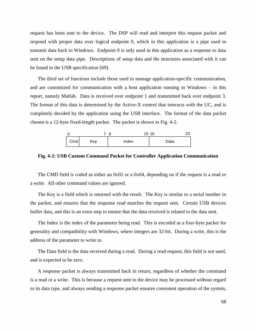
68
request has been sent to the device. The DSP will read and interpret this request packet and
respond with proper data over logical endpoint 0, which in this application is a pipe used to
transmit data back to Windows. Endpoint 0 is only used in this application as a response to data
sent on the setup data pipe. Descriptions of setup data and the structures associated with it can
be found in the USB specification [69].
The third set of functions include those used to manage application-specific communication,
and are customized for communication with a host application running in Windows – in this
report, namely Matlab. Data is received over endpoint 1 and transmitted back over endpoint 3.
The format of this data is determined by the Active-X control that interacts with the UC, and is
completely decided by the application using the USB interface. The format of the data packet
chosen is a 12-byte fixed-length packet. The packet is shown in Fig. 4-2.
DataIndex
70 8 15 16 23
KeyCmd
Fig. 4-2: USB Custom Command Packet for Controller Application Communication
The CMD field is coded as either an 0x02 or a 0x04, depending on if the request is a read or
a write. All other command values are ignored.
The Key is a field which is returned with the result. The Key is similar to a serial number in
the packet, and ensures that the response read matches the request sent. Certain USB devices
buffer data, and this is an extra step to ensure that the data received is related to the data sent.
The Index is the index of the parameter being read. This is encoded as a four-byte packet for
generality and compatibility with Windows, where integers are 32-bit. During a write, this is the
address of the parameter to write to.
The Data field is the data received during a read. During a read request, this field is not used,
and is expected to be zero.
A response packet is always transmitted back in return, regardless of whether the command
is a read or a write. This is because a request sent to the device may be processed without regard
to its data type, and always sending a response packet ensures consistent operation of the system,

69
removing the type of command from the behavior. If the command sent is a command to write
data, the response packet is the same as the incoming packet. Otherwise, if the response packet
is a request to read data, then the response packet will contain the result of the inquiry. Either
way, the response packet contains the current value of the register.
It is important to note that a protocol has been put in place that runs concurrently with the
actual operation of the system, and it is important to remember that data dependent on other data
(which must change in a single atomic operation) must be enforced by the application. Such is
the case when changing the gain of a controller, as one generally cannot change the proportional
gain first, and then the integral gain at a later time. Both must be changed simultaneously. This
does affect the operation of the system when using the PLL, but the order of changes can be done
such that the dependent data is not changed while it is active.
After the parameter array has been updated, a function is called to update the application with
the new parameters. The parameters are always sent as 32-bit integers, but the data in the
application is usually in floating point format. The scaling factors are one function of this update
function, UpdateParameters(). A second purpose of this function is to move pointers. In this
application, different data are sent out via the analog interface, depending on which stage of the
measurement the application is in. There are several ways to handle this. The most intuitive, but
least efficient way of doing this is to use a very large case statement inside the interrupt service
routine, where a parameter indicates which index to use, and thus which case to execute.
A more efficient way is to dereference a pointer which points to the output variable of
interest. This is the approach taken here, and the pointer is set by the USB function. It is
acceptable that this pointer is moved asynchronously to the application, as the application does
not measure when the pointer is moved, making the output value unobserved during this
transition. The pointer is still assigned by looking up the value of the parameter of interest in a
case statement – the difference being that this case statement does not have to execute within the
time constraints of the interrupt service routine. The list of parameters that can be observed is
shown in Table 4-2.

70
Table 4-2: Index Parameters
Index Variable Description
1-18 fInputV[n-1] (n is index) Data from ADC
20 fVd d-,q-,or 0- channel voltage
(scaled by sensor) 21 fVq
22 fV0
23 fVa Va, Vb, or Vc voltages as read by
sensor (line-to-line or line-to-
neutral, depending on parameter
9 setting)
24 fVb
25 fVc
30 fILd d-, Q-, or 0- channel currents
(scaled by sensor) 31 fILq
32 fIL0
33 fILa ILa, ILb, or ILc currents as read
by sensor (line-to-line or line-to-
neutral, depending on parameter
9 setting)
34 fILb
35 fILc
40 fPert Perturbation reference from
analyzer RF OUT terminal
42 fVqInt PLL Vq Integral Component
45 fVtest0 Square wave that toggles each
time the interrupt is called
56 VsdnBar
PLL states for positive and
negative sequence D- and Q-
channel components
57 VsqnBar
58 VsdmBar
59 VsqmBar
63 fIPaRef Reference outputs that are to be
sent to controller 64 fIPbRef
65 fIPcRef
99 cfCosWt Cosine component of transform

71
C. Interrupt Handler (Algorithm)
The interrupt handler executes the main loop, and implements the signal flow diagram shown
in Fig. 4-3.
Fig. 4-3: Signal flow diagram for interrupt handler
The parameters shown that do not flow from the analog-to-digital converter (ADC) are set
via communication with the PC. Injection is controlled via the IpdGain and IpqGain. Setting
both of these to zero disables injection. The Lock variable determines whether the PLL acquires
the voltage vector or maintains a lock. This is set via the graphical user interface.
The interrupt handler monitors its own execution period in CPU clock cycles. This is
important when coding to ensure that adding code does not cause an overflow, and that the
interrupt occurs at a fixed sampling frequency. Variation in the sampling frequency will lead to
improper operation of the digital filters, and will produce transfer functions which are not
intended in the design. Such a problem may lead to harmonic injection and stability issues, most
specifically with the phase-locked loop.

72
III. FPGA Firmware
A. Architecture
The FPGA provided on the universal controller is its core. All peripherals are connected via
this FPGA, including the analog interface PCB described earlier. For detailed information on the
architecture of the FPGA code and its core components, one may read [61]. Described here is
the digital interface and communication processing used to interact with the measurement PCB.
As mentioned above, all peripherals are connected via a serial peripheral interface bus (SPI).
From this bus, the controller has a module that processes the data and control signals specific to
each device in a VHDL-based device driver [70] which makes the data available to the DSP so
that it may be read and processed by the interrupt-based DSP code. The architecture of the
VHDL code relevant to this piece is shown in Fig. 4-4.
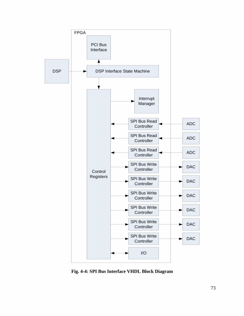
73
SPI Bus Read
Controller
SPI Bus Read
Controller
SPI Bus Read
Controller
Interrupt
Manager
Control
Registers
SPI Bus Write
Controller
SPI Bus Write
Controller
SPI Bus Write
Controller
SPI Bus Write
Controller
SPI Bus Write
Controller
SPI Bus Write
Controller
I/O
DSP Interface State Machine
PCI Bus
Interface
DSP
ADC
ADC
ADC
DAC
DAC
DAC
DAC
DAC
DAC
FPGA
Fig. 4-4: SPI Bus Interface VHDL Block Diagram

74
IV. Matlab Software – Algorithm and Instrumentation Interface
A. Architecture
Matlab code is written based on scripts and functions. The code is separated into functions
related to the algorithm execution, functions related to instrument control and configuration,
functions related to data storage and retrieval, functions related to the graphical user interface
and results presentation.
B. Algorithm
The algorithm is controlled via the ZDQ_MEAS_MAIN script. This script calls all
measurement acquisition functions and computes the impedance based on these measurements.
The scripts related to algorithm are responsible for determining the configuration state of the
gain/phase analyzer as well as the output being measured. After scripts related to the algorithm
have executed, the impedance is available as an frequency response data (FRD) object in
Matlab.
Using the messaging scheme discussed above, messages are sent to the GPIB instrument and
to the digital signal processing subsystem to control the sweep and coordinate inputs and outputs.
Fig. 4-5 is shows the messaging between the controller subsystem and the digital signal
processing subsystem, as well as the controller subsystem and the gain / phase analyzer used to
identify the impedance. Each message is described below:
Reset. This message resets the gain / phase analyzer to the default state.
Configure I/O. This sets the input and output paths of the digital processing subsystem to
inject the perturbation at the correct angle in the DQ space and to transmit the correct DQ
variable to the gain/phase analyzer for transfer function identification.
Configure Sweep. This message is sent to the gain/phase analyzer and is used to set the
sweep parameters, such as the start and stop frequencies, the IF bandwidth, the number of
points, and, if used, the averaging.
Enable Injection. This writes the gain values that enable the instrument to inject a
perturbation.
Sweep. This command starts the process which identifies the transfer function.
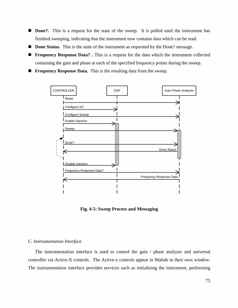
75
Done?. This is a request for the state of the sweep. It is polled until the instrument has
finished sweeping, indicating that the instrument now contains data which can be read.
Done Status. This is the state of the instrument as requested by the Done? message.
Frequency Response Data? . This is a request for the data which the instrument collected
containing the gain and phase at each of the specified frequency points during the sweep.
Frequency Response Data. This is the resulting data from the sweep.
DSPCONTROLLER Gain Phase Analyzer
Configure Sweep
Reset
Sweep
Done?
Done Status
Disable Injection
Enable Injection
Frequency Response Data?
Frequency Response Data
Configure I/O
Fig. 4-5: Sweep Process and Messaging
C. Instrumentation Interface
The instrumentation interface is used to control the gain / phase analyzer and universal
controller via Active-X controls. The Active-x controls appear in Matlab in their own window.
The instrumentation interface provides services such as initializing the instrument, performing

76
and monitoring sweep status, and importing data from the analyzer and interpreting it into
frequency response data objects.
D. Data Management Scripts
Data management scripts are responsible for the storage and recall of data from the results
directories in which each sweep is stored. The stored data makes use of universally unique
identifiers (UUIDs), which are used to recall the data. The scripts used for generating UUIDs are
also included here. Data can be recalled from the results directory via scripts that search the
results for the matching UUID.
V. Matlab Software – GUI and Data Storage
A. Graphical User Interface
The graphical user interface is a tabbed dialog with a menu. Most of the functionality of the
graphical user interface is designed to view the results of sweeps, recalling descriptions, dates,
globally unique identifiers (GUIDs), and plots of the sweeps. The first tab allows the user to
select the impedance based on the date and time it was taken via a list box. Upon selecting the
impedance, the channels are shown in small bode plots on the same tab, and information about
the impedance is loaded into an edit box adjacent to the list box. When this selection changes,
other tabs in the dialog change as a result. The second tab shows the currents measured during
the sweep. The third tab shows the voltages measured during the sweep. The fourth tab shows
the individual impedances. The first four tabs display results as governed by the first tab, where
the user selects the results to be displayed. The fifth tab allows the user to measure individual
SISO transfer functions and view their results, and can be considered a separate function. The
results of the SISO transfer functions are stored and accessible in a similar fashion to the D-Q
impedances.

77
Fig. 4-6: Graphical User Interface

78
Fig. 4-7: Currents as displayed on current tab. The currents are those used to measure the
impedance which is selected in the first tab, labeled Results Viewer.
B. Data Storage
The structure of the measurement file system is shown in Fig. 4-8.

79
Fig. 4-8: Directory Structure of Impedance Measurement Software
The measurement results are stored in Results 1X1 for the SISO transfer function
measurements and Results for D-Q impedances. Upon measuring the impedances, the Matlab
script PERSIST_DATA will store the results into a .mat file located in a subfolder in either
RESULTS1X1 or RESULTS. The script will also store a text version of the same data, and
optionally plots of the impedances and measured voltages and currents. As this takes a
significant amount of space, it is disabled, but can be easily added via a data maintenance script.
Binary executables are stored in the Bin subdirectory, and its subdirectory sys stores the
device driver used with Windows, although Windows will copy this driver upon installation.
Matlab contains the scripts used, and is the directory from which the system operates.
VI. USB Interface
A. Short Review of Active-X Controls and COM
As Active-x controls are used in the architecture for simplicity, it is instrumental to briefly
discuss them, how to create them, and how to use them. It is assumed the reader has familiarity
ZMEAS
Matlab XML Toolbox
Results 1X1RESULTS_YYYYMMDD_H
HMMSS
ResultsRESULTS_YYYYMMDD_H
HMMSS
Bin SYS

80
with object-oriented programming and understands concepts such as pointers, object
construction and destruction, and is somewhat familiar with Windows and the registry.
COM [71] is a subsystem in windows that allows pre-existing objects to be directly loaded
into memory and interfaced without having to compile them at runtime for each application. An
object may exist in one of three places:
In the calling process (called a container/the containing process), known as an in-proc
server
On the same machine as the calling process, called a local server
On a remote machine (giving rise to Distributed COM, or DCOM), called a remote server
Prior to use, an object must be registered with Windows. This is done at the command
line by calling RegSvr32 followed by the process name if the object is stored in a dll, or by
calling the executable with the switch /RegServer if the object is an executable. Performing this
function makes windows aware of the object, and places information about it in the windows
registry (in the hive HKEY_CLASSES_ROOT). Along with this information is a string known
as a globally unique identifier (GUID) or a UUID, hereafter simply referred to as GUID.
When a client process wants to use the object, it makes a call to Windows and “asks”
windows for this object by providing the object‟s GUID as the only identifying parameter.
Windows then looks up in the registry the location of the object and creates the object as
specified in the function call (whether it be in process. local or remote). Along with the object,
the calling process specifies an interface to be requested; this is discussed later. The code is then
loaded by Windows in the appropriate location, and a pointer is given to the calling process
representing that object.
An object may have several interfaces. Each interface is functionally distinct in that it is
designed to assist the calling process in performing tasks. For example, an object that processes
data may provide two interfaces. One interface to add and remove data and to perform
computations, and a second interface to store and load that data to or from a disk. The object is
the same, and the data is the same, but the objectives of the two interfaces are different; one deals
with the values of the data itself, and the other deals with the objects‟ persistence. These two
interfaces have two different interface IDs (referred to as IIDs). Some interfaces are accessed
81
mostly by the user while others are directly managed by Windows or the container (as in the
cases we will describe). Thankfully, the infrastructure provided by Microsoft provides the basic
functionality and implements most of the functions necessary to make the object work in simple
containers, alleviating the user from having to perform this task.
To program such an object, one has many choices, but usually makes use of one of two ways
to do it, mostly either the Microsoft Foundation Classes (MFC) or the Active-X Template
Library (ATL). ATL was chosen for this application for several reasons, including its light
weight and my familiarity with its use. The ATL wizards provided by Microsoft in Visual
Studio 2005 make it very simple to program such an object, allowing the programmer to focus
mostly on the functional code, and not on the mechanics of the implementation.
To further simplify this, the objects created in the application we are using contain a
dispinterface [71]. This interface implements an interface called IDispatch, allowing programs
such as Matlab to access functions in the object simply using user-friendly names, and allows
their use in Matlab to be as simple as that of a class in C++ or visual basic. To display the object
and manage its instantiation, Matlab calls other interfaces, but these are beyond the scope of this
report, and are not necessary to describe the concept of the object‟s operation. Active-X controls
as considered in this report are to be thought of as in-proc server COM objects with a
dispinterface.
B. COM as Used in This Architecture
Two Active-X objects are created in this architecture. One is used to manage the USB
interface via Matlab, and the other is used to manage the GPIB interface via Matlab. The
Active-X object in Matlab for GPIB does access a local (or remote) COM server which
implements the NI-488 API.
Matlab has intrinsic commands to create Active-x objects, specifically actxcontrol and
actxcontrollist. Once the object is created in Matlab, it appears and is accessed just like one
would access a class in C++. Matlab hides some of the details of the data type transmission,
such as moving arrays and strings between the object and the Matlab script, represented by
SAFEARRAYS and BSTRs.

82
C. USB Active-X Dispinterface
There are three primary functions provided via the dispinterface of the USB Active-X
control:
One function to write data to the DSP
One function to read data from the DSP
One function to open a connection
The connection is closed upon destroying the object in Matlab. This is performed by clearing
the associated variable representing that object and closing its associated host window, as Matlab
places Active-x controls in a host window. Due to delays, one should call these functions twice
in a row. Upon calling the read function, the parameter being read is returned to the user as the
return value.
No error checking is implemented programmatically and made available to the user from
these functions, but errors will interrupt the program and return failure codes. Additionally,
errors will be written to the debugging window and to a log with a description of the error. If a
read or write function is called prior to opening a connection, the Active-X control will attempt
to open the connection when the read or write function is called, and the connection will remain
open throughout the lifetime of the object.
D. USB Interface Software
Certain operations involve human interaction, such as setting the PLL frequency and the
analyzer modes of operation. These modes can be set via a small modal dialog application
developed using Microsoft Foundation Classes (MFC). The dialog also demonstrates the use of
the USB Active-X control, which can be seen in the lower right hand corner of Fig. 4-9.
A second Active-X control, MS FlexGrid (a Microsoft Active-X, msflxgrd.ocx, which must
be registered on the system) is used to produce the list of parameters seen on the left-hand side of
the dialog box in Fig. 4-9. This Active-X is located in the system32 folder in the system
directory. The parameters are the same set of parameters used by Matlab to control the injection.
They may be monitored from this window, and changed if necessary.

83
Fig. 4-9: Software used to set UC parameters directly via USB. The parameters sent to the
controller can be seen in the grid on the left hand side. The parameters may be changed
using the controls in the group box labeled Set, and read by pressing Acquire. The USB
Active-X control can be seen in the lower right hand corner.
This application demonstrates the need for a mutex [72].. If the mutex is not present, one
may request a read from this application while Matlab is simultaneously requesting one. The
command packet sent to the controller requesting the read from this application may be
accidentally sent to Matlab if there is no synchronization that controls access to the application.
As this synchronization is implemented in the Active-X, it is transparent to both applications,
which are unaware of each other.
VII. GPIB Interface
The GPIB interface makes use of the NI-488 API to communicate with instrumentation.
Matlab is used to coordinate this communication via Active-X objects written for this purpose in
C++ using the Microsoft Active-X template library (ATL). The GPIB interface was
implemented as an ATL-based COM (Component Object Model) server, and made use of
DCOM in order to avoid driver conflicts on the original PCs used to do the tests. The end

84
solution involved a single PC, and due to the nature of the implementation of COM, the changing
from a local process to a remote one is done by simply calling a different function.
VIII. Summary and Conclusions
We have written software to implement the control and communication functions required by
a three-phase impedance analyzer. The architecture is a hybrid architecture consisting of
elements written in C++, VHDL, and Matlab, and is implemented on a DSP, FPGA, and a PC
running Windows XP.
Data storage functions have been implemented to allow the persistence of the acquired
impedances to disk. Via the use of GUIDs, these results may be later recalled in to Matlab
programmatically or via a graphical user interface developed for this purpose.
The impedance calculations are performed in Matlab. Communication with other
instrumentation, including the customized hardware developed during this project, is performed
using Matlab‟s ability to instantiate Active-X controls. There are two controls to facilitate this --
one control for GPIB and another for USB. The GPIB control communicates with an out-of-
process COM server written for this project, which in turn communicates with the GPIB
instrument. The USB control communicates with a customized USB device driver designed for
the universal controller and developed during this project. The device driver is based off the
Bulk USB driver developed by Microsoft. This driver communicates with the IC on the large
PCB developed for this project, which in turn communicates with the DSP, ultimately adding
plug and play capability to the universal controller as well as a communication interface used to
modify parameters in the DSP directly. We developed a simple protocol to facilitate this.
We‟ve written FPGA code to support the serial peripheral interface of all peripherals,
transferring data to and from the devices to memory-mapped control registers readable by the
DSP for use in the control algorithm and communication. The FPGA code was written in
VHDL.
We wrote additional supporting software to facilitate debugging and logging via a dedicated
output window. We also wrote additional Matlab software to analyze specific results acquired
during the verification procedure.

85
Chapter 5. Verification and Test
I. Introduction
After constructing the instrument it is necessary to produce a model of it based on
measurements, and verify the model‟s operation. There is, however, an obstacle which prevents
one from directly measuring the results and immediately knowing whether the model is accurate.
This obstacle is the fact that the impedances being measured are unknown, so the reference as to
what is the correct impedance (measured by other means) starts out undefined. DQ impedance,
as is well-known and mentioned in Chapter 1, is not physically measurable, and no instrument
previously constructed can measure it with confidence enough to establish a standard.
Therefore, the first challenge in verification involves identifying the correct impedance with
which to compare the results of the measurement instrument.
There is, however, a solution for linear, time-invariant impedances. If one acquires the
impedance in the stationary (ABC) frame and assumes symmetry across all phases, the correct
impedance DQ impedance can be determined. This relationship is derived in Section II of this
chapter.
Section III defines a model of the tester derived from piecewise component analysis, relating
the transfer functions measured in Chapter 3 back to the actual instrument, and indicating their
contribution to the effect on the measured impedance.
Section IV takes the results from Section II and uses them to first deduce the correct DQ
impedance from the measured impedance of linear networks in the ABC domain, and then uses
this measurement to validate the instrument‟s measurement results.
As the previous technique is only applicable to networks which start out measurable in
stationary coordinates, it is the only criteria used to validate the instrument‟s operation. In the
case of nonlinear networks, it is not as easy to use these as examples to validate the instrument,
as the results are unknown. Many papers propose ideas on what the impedance of these
networks should be, and in some cases these are used in this section to validate what is known

86
about the impedance as suggested in these papers. Section V presents the results of measuring
these nonlinear networks.
Section VI presents the conclusions of this chapter.
II. Model of an ABC Domain Transfer Function as Seen in the DQ Space
In order to compare results of known impedance, a mechanism must be in place which can
take results measured for linear impedances in the stationary frame and compute their equivalent
DQ impedance. This section develops the basis for this transformation, focusing on systems
which are balanced, three-phase systems. Furthermore, this paper only focuses on three-phase
systems without the presence of zero-sequence dynamics (where the voltages and currents of all
three phases sum to zero).
Traditionally, this is approached by analyzing the state-space model of a the system in
stationary coordinates in the time domain, and then finding the equivalent state-space model in
D-Q in the time domain, and then transforming that model to the frequency domain. This
analysis must be performed on a case-by-case basis, requiring re-derivation whenever the model
changes.
It is, however, possible to perform this time-varying transformation without ever utilizing the
time domain, and using strictly frequency domain models, as is shown and demonstrated in this
section.
A. Notation and D-Q representation of three-phase variables
The three-phase line currents and voltages are represented as a vector in the ABC domain
and the D-Q domain as follows:
, (33)
The D-Q transformation used in this work is repeated here for the reader‟s convenience:

87
(34)
where is the frequency of rotation.
Since we are not considering the zero sequence, , and thus the
inverse transformation can be defined as its transpose:
(35)
In a three-phase system, dynamical subsystems often exist in a three-phase system on a per-
phase but symmetric basis. These subsystems can be represented by a diagonal matrix of
transfer functions. We will define the frequency domain 3x3 matrix operator as
(36)
If we were to view these dynamics from the D-Q frame, we would see the dynamics as described
in Fig. 5-1.
Habc(s)
D-Q
ABC
xd(t)
wt
xq(t)
xa(t)
xb(t)
xc(t)
L
L
LXc(s)
Xb(s)
Xa(s)
Yc(s)
Yb(s)
Ya(s)L-1
L-1
L-1
ya(t)
yb(t)
yc(t)
D-Q
ABC
wt
yd(t)
yq(t)
Fig. 5-1: DQ Representation of ABC domain Transfer Function

88
For dynamics such as those described in (36), one can envision an equivalent small-signal,
time-invariant model in the D-Q domain, described by these dynamics as:
Hdq(s)
Xd(s)
Xq(s)
Yd(s)
Yq(s)
Fig. 5-2: System Represented in DQ Coordinates
where is a 2x2 matrix operator:
(37)
There is a relationship between the elements in the two system descriptions shown in (36) and
(37), which is the topic of this section.
B. Example Systems
The following examples will be used as a reference throughout this chapter to provide an
intuitive example.
i) Inductive Load
A three-phase wye-connected resistor inductor represented in the ABC domain has a per-
phase impedance . The three-phase impedance of the system in ABC
coordinates can be represented as
(38)
where is the identity matrix. Note that this system directly matches the form of (36).
ii) State Space System
A three-phase wye-connected impedance matrix can be represented as a state-space system
of the form

89
(39)
(40)
This system is an aggregated form of (3) where each element in matrix 3 is represented by the
state-space system
(41)
for some order of system , making
(42)
(43)
C. Symmetrical Transfer functions in the ABC Domain as seeniIn the DQ Domain
Converting to and from the ABC domain transfer functions to the D-Q domain involves a
time-domain multiplication of the D-Q matrix, which is a convolution in the frequency domain
between the variable and the transformation.
This can be shown graphically in the following two diagrams:
H(s)
H(s)
H(s)
D-Q
ABC
ya
yb
yc
xa
xb
xc
xd
xq
Fig. 5-3: Transforming to ABC Coordinates and Applying H
It is important to note here that is the same transfer function applied to each phase. To
allow the transfer function to pass to the D-Q domain, we would like to “pull” H(s) through the
transformation, so while keeping the same inputs and outputs, we would instead produce:

90
D-Q
ABC
ya
yb
yc
xd
xq
Hdq(s)
yd
yq
Fig. 5-4: Applying Hdq and Transforming to ABC Coordinates
where is the 2x2 matrix of transfer functions described in (37).
If the transformation was were a time-varying one, and were, instead, a time-invariant
transformation, one can immediately get the model via a similarity transformation. As an
example, consider the invertible time-invariant transformation matrix T.
Given
(44)
(45)
one can construct a new basis function such that:
(46)
(47)
As is not time-variant, it follows that:
(48)
(49)
Similarly,
(50)
Simple substitution shows that the equivalent system dynamics in the new domain yields:

91
(51)
(52)
However, as the matrix described in (34) is also an explicit function of time, we have less
freedom with respect to how we can transform our system:
(53)
(54)
but instead
(55)
where denotes convolution.
It is therefore not as easy to separate from , as we did in the previous solution.
One potential solution to the problem takes advantage of the fact that the form of the elements of
are sinusoidal, and thus one can apply the modulation property of the Laplace transform
to simplify the results.
D. Sinusoidal Modulation in the Frequency Domain
Given a three-phase variable in the DQ domain, the equivalent representation of the matrix in
the ABC domain can be described by applying the modulation property of the Laplace
transformation of the DQ variable to the ABC domain.
Let us consider the vector to be the original variable transformed to the ABC domain
by (35). In the time domain, the component can be expressed as
, which is and undergoing cosine and
sine modulation, respectively.

92
In constructing the complete operator that will transform our system, it is useful to construct
smaller operators for compactness. If we define a cosine modulation operator such that
where :
(56)
and a sine modulation operator such that where
:
(57)
then can be represented as
(58)
To simplify the conversion of other phases, it is also useful to define equivalent operators for
the phase-shifted cosine and sine modulation (for example, and similar terms) in
terms of their trigonometric representations, , and re-apply the above-
mentioned operators directly with the coefficients, instead of needing to define new operators for
the phase-shifted modulations:
(59)
(60)
(61)
(62)
which correspond to multiplication of by , , and
, respectively. The Laplace transform of the components of the vector can
then be expressed as:
(63)

93
(64)
(65)
Next, applying to each ABC frequency domain variable yields the ABC frequency
domain outputs, .
The result obtained after applying can now be transformed back to the D-Q domain by
the inverse transform, applying the same modulation properties just described to the ABC
domain output . The expressions become rather complex, but the results can be simplified.
Following this simplification, we can derive based on these modulation properties the simplified
equivalent system in the D-Q domain directly to be:
(66)
which is the key contribution of this section.
E. Application to example
Returning to the example of the inductor, we can calculate the D-Q impedance,
using this method. By substitution,
(67)
(68)
Thus we can verify the D-Q impedance of an inductor to be
(69)
F. Properties of Transformed Matrices
T he matrices resulting from transformation (33) have a notable form, with equal diagonals and
equal anti-diagonals with opposite signs. Matrices of this form comprise a field referred to in
this paper as :

94
(70)
Matrices of this structure form field. Some notable properties of these matrices are:
i) Closure under addition
Two matrices A and B belonging to are added to create a third matrix, C=A+B, also in this
group.
ii) Closure under multiplication
Two matrices A and B belonging to create a third matrix C=AB, also in .
iii) Commutativity
Two matrices A and B belonging to have a product which is invariant to the order of the
matrices. That is, .
The first three properties can be proven by algebraically expanding the matrices and
showing that the form of the results matches the form required for membership in .
iv) Closure under multiplicative inversion
A matrix A belonging to will yield an inverse which is also a member of . This can be
shown by taking any matrix in , such as
(71)
where , and computing its inverse:
(72)
The resultant matrix also follows the form of elements of , indicating closure under inversion.
v) Closure of feedback-interconnected systems
It follows from the above properties that if there is a closed-loop system consisting of G and
H, then the resulting feedback interconnected system , will also be a member of .
(73)
where is the identity matrix, also a member of , serving as the multiplicative identity
element.

95
G. Application of Field Properties
Application of these properties allows us to explore more parallels between the D-Q domain
and the ABC domain.
It is intuitive that in the ABC domain, the per-phase single input, single output transfer
functions are commutative, and different elements of each phase may be re-ordered without
changing the system response. Following this, the same elements now represented in the D-Q
domain may be re-ordered without changing the D-Q domain frequency response due to the fact
that members of commute.
Since most of the power electronics components prior to and after the switching converter
but before the D-Q transform in the control loop are of this form, it is possible to simplify system
representations using these properties.
H. Symmetrical State Space Models in the ABC Domain as seen In the DQ Domain
Fitting frequency-domain data to known forms of transfer functions, as is often done in
component approximations, is both tedious and error-prone. Alternatively, direct frequency
domain measurements of a transfer function can be taken in the ABC domain using equipment
such as a gain/phase analyzer or a network analyzer, and the resulting data may then be fit to a
generic state-space model of sufficient order using one of the many available tools designed for
this purpose. From the generic state-space model shown in this section, we show that there is an
equivalent state-space model in the D-Q domain.
I. Phase State Space Model Transformation to D-Q
Given a state-space model of a phase of the balanced system, with each phase having a
transfer function described by the following equations.
(74)
the model can be transformed to the D-Q domain by applying (66) and reducing:

96
(75)
where is , and and are the new states of the system.
i) Preservation of System States
The original system in the ABC domain had transfer functions, each with n states. It is seen
above, however, that the number of states has been reduced from 3n to 2n. The reader is
reminded that these methods hold for balanced, symmetrical systems with balanced, three-phase
symmetrical perturbations where the zero sequence is never excited. The system models are
therefore on the planar subspace . Therefore, one of the states of
the ABC system is completely specified by the other two at any instant in time. Thus the number
of states of the system is preserved from the ABC domain when transforming to the D-Q
domain, and is equal to two times the total number of states representing any single phase of the
three-phase system. From the linearity property of the Laplace transform, we see that
.
ii) Application to Example
The example with inductors may be transformed into a state-space system and used to
demonstrate this mode of transformation:
(76)
(77)
where is the equivalent series resistance of the inductor, is its inductance, is the
Laplace transform of the three-phase voltage vector across the inductors, and is the
corresponding three phase current vector. The output equation is trivial.
Conversion to the D-Q domain via the procedure described above yields the following:

97
(78)
which can be recognized as the impedance of an inductor in the D-Q frame available in many
texts.
J. Extension to Non-Diagonal ABC Domain Transfer Functions
The constraint on the system that the transfer functions must be in a wye configuration, while
common, can limit the application of these techniques. There is a second form of ABC domain
transfer function that may be also directly transformed to the D-Q domain. Given a transfer
function matrix of the form:
(79)
when transformed to the alpha-beta domain (in this paper defined as the DQ domain where
) yields
(80)
This is equivalent to the system,
(81)
which yields an identical result.
K. Application to Power Electronics-based Three-Phase Converters and their Elements
Three-phase power converters have subsystems and effects which are applied to each phase
independently. Two of these, the anti-aliasing filters and the digital delay, have transfer

98
functions that can be derived in the D-Q domain from the given ABC domain transfer functions,
and are demonstrated here.
i) Anti-aliasing Filter
An anti-aliasing filter is typically used in such a converter to remove components of the
signal that are of a higher frequency than the sampling frequency. Such a filter is often
implemented as a simple second order Butterworth filter. This model can be expressed as:
(82)
The corresponding representation in the D-Q frame rotating at frequency may be found by
modeling this filter in state space as follows:
(83)
Upon transforming this filter using the method described in Section IIIA., the resulting filter in
the DQ domain becomes:
(84)
ii) Digital Delay
The digital delay can be modeled in stationary coordinates as:
(85)
Upon applying the modulation operators (56) and (57), one can find via Euler identities that:
=
(86)

99
=
(87)
Applying these results in (33) yields:
(88)
One may recognize the coefficient matrix as a rotation operator, rotating the input vector by an
angle of radians. T is typically one or two sample periods for a digitally controlled
converter.
III. Characteristics of System under Test
Using the system descriptions above, one may construct the following block diagram of the
system used during a single sweep in the D-Q domain. Radial symmetry is assumed among the
components comprising one block. Transfer functions starting with „H‟ are continuous-time
systems. Transfer functions starting with „G‟ represent discrete time systems, and are
implemented either in the DSP or FPGA.
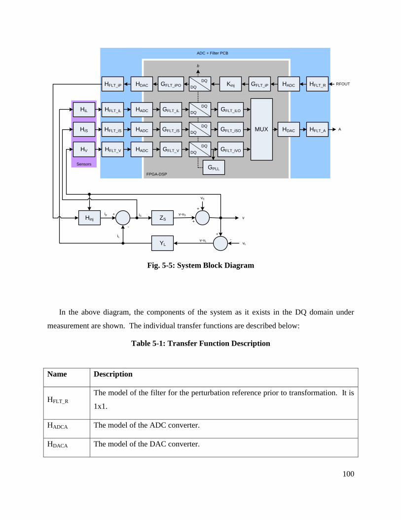
100
ZS
YL
v
vL
iS
iLv-vL
v-vS
vS
+
+
+
+
-
-
Hinj
ip
HiS
HiL HFLT_iL
HFLT_iS
HADC
HADC GFLT_iS
GFLT_iL DQ
DQ
DQ
DQ
HV HFLT_V HADC GFLT_V DQ
DQ
GPLL
GFLT_iPOHDACHFLT_iP
GFLT_iSO
GFLT_iLO
GFLT_iVO
MUX HDAC HFLT_A
HFLT_RDQ
DQHADCGFLT_iPKinj RFOUT
A
b
FPGA-DSP
ADC + Filter PCB
Sensors
Fig. 5-5: System Block Diagram
In the above diagram, the components of the system as it exists in the DQ domain under
measurement are shown. The individual transfer functions are described below:
Table 5-1: Transfer Function Description
Name Description
HFLT_R The model of the filter for the perturbation reference prior to transformation. It is
1x1.
HADCA The model of the ADC converter.
HDACA The model of the DAC converter.

101
Name Description
HFLT_A The model of the output filter to the gain/phase analyzer.
HFLT_iP The model of the output filter to each amplifier from the DAC reference.
HFLT_iL The DQ model of the model of the filtered load currents prior to DQ
transformation.
HFLT_iS The DQ model of the model of the filtered source currents prior to DQ
transformation.
HFLT_V The DQ model of the model of the filtered voltages prior to DQ transformation.
HADCD The DQ model of the ADC converter.
HDACD The DQ model of the DAC converter.
HiL The transfer function of the load current sensor.
HiS The transfer function of the source current sensor.
HV The transfer function of the voltage sensor.
GPLL The model of the PLL dynamics on the DQ frame during injection.
GFLT_iLO A filter in the DQ domain after transformation. It is optional and was represented
as a scalar in the implementation, but may be a transfer function in other designs.
GFLT_iSO A filter in the DQ domain after transformation. It is optional and was represented
as a scalar in the implementation, but may be a transfer function in other designs.
GFLT_iVO A filter in the DQ domain after transformation. It is optional and was represented
as a scalar in the implementation, but may be a transfer function in other designs.
GFLT_iL The input filter for the measured load currents. It is 2x2.
GFLT_iS The input filter for the measured source currents. It is 2x2.
GFLT_v The input filter for the measured voltages. It is 2x2.

102
Name Description
GFLT_iP The input filter prior to the DQ transformation. It is 1x1.
GFLT_iPO The output filter of the perturbation reference. It is diagonal 2x2.
Kinj A 2x1 vector which determines the angle at which to inject.
Hinj The transfer function from the injection reference to the current injected into the
system.
ZS The source impedance.
YL The load admittance.
The model can be simplified by eliminating the elements that switch each time the transfer
function is measured. This can be done with the understanding that the multiplexer just selects
an input to present on the output. Since the system is time-invariant, the multiplexer can be
eliminated by creating three outputs, on for each of the corresponding multiplexers. In this new
representation, A becomes the three outputs, namely A_iLO, A_iSO, and A_VO, representing
the load current, source current and voltage, respectively, as presented to the gain/phase
analyzer.
Secondly, Kinj can be eliminated by creating a second input, which represents perturbations
on the other channel. Kinj was a 2x1 matrix that projected the perturbation onto a vector in the
DQ domain. As described in Chapter 4, for each perturbation, it was changed to project the
disturbance at another angle in the D-Q space. It can simply be replaced here by two inputs –
one on the D-axis and one on the Q-axis, referred to as RFOUT_d and RFOUT_q, respectively.
Combined together as a vector, these will be referred to as Rdq. It is still shown in Fig. 5-6 as
Kinj2x2, but is equal to the 2x2 identity matrix with both input channels explicitly shown.

103
ZS
YL
v
vL
iS
iLv-vL
v-vS
vS
+
+
+
+
-
-
Hinj
ip
HiS
HiL HFLT_iL
HFLT_iS
HADCD
HADCD GFLT_iS
GFLT_iL DQ
DQI
DQ
DQI
HV HFLT_V HADCD GFLT_V DQ
DQI
GPLL
GFLT_iPOHDACDHFLT_iP
GFLT_iSO
GFLT_iLO
GFLT_VO
MUX HDACA HFLT_A
HFLT_R
DQ
DQI
HADCAGFLT_iP
Kinj2x2
RFOUT_d
A_iSO
b
FPGA-DSP
ADC + Filter PCB
Sensors
HDACA HFLT_A A_iLO
HDACA HFLT_A A_VO
HFLT_RHADCAGFLT_iP RFOUT_q
Fig. 5-6: Modified Block Diagram with All Inputs and Outputs
The model can be further simplified. If the injection system is good, and follows the
reference, then the loop containing Hinj (the effect of the voltage on the injection system) can be
eliminated. Also, if the PLL is extremely slow, then the loop containing GPLL can be eliminated:

104
ZS
YL
v
vL
iS
iLv-vL
v-vS
vS
+
+
+
+
-
-
Hinj
ip
HiS
HiL HFLT_X
HFLT_X
HADCD
HADCD GFLT_iS
GFLT_iL DQ
DQI
DQ
DQI
HV HFLT_X HADCD GFLT_V DQ
DQI
GFLT_iPOHDACDHFLT_iP
GFLT_iSO
GFLT_iLO
GFLT_VO
HDACA HFLT_A
HFLT_R
DQ
DQI
HADCAGFLT_iP
Kinj2x2
RFOUT_d
A_iSO
FPGA-DSP
ADC + Filter PCB
Sensors
HDACA HFLT_A A_iLO
HDACA HFLT_A A_VO
HFLT_RHADCAGFLT_iP RFOUT_q
Fig. 5-7: Simplified System
After simplifying the model, the following equations can be written as shown in Chapter 2.
For compactness they have each been given a transfer function definition:
(89)
(90)
(91)
Using the above model, the following equations can be written:
(92)
(93)
(94)
(95)

105
For compactness of notation, we define the following:
(96)
Another assumption that shall be made based on the design of the hardware is that all the anti-
aliasing filters are identical. That is,
(97)
So that:
(98)
(Remembering that is ).
Combining (98) with (89) gives:
(99)
Repeating for the currents:
(100)
(101)
Simplifying , , , , , and to be their respective
constants as used in this application: , , , , , and , and
combining with (97):
(102)
Again combining terms for compactness one can define:
(103)
And constants , ,
This gives rise to the following:
(104)
(105)

106
(106)
from which if one computes the impedance (estimated, so denoted ) using the results obtained
from the analyzer, one gets:
(107)
(108)
IV. Tests used to Validate Operation
Linear impedances are favorable to use as a standard which can be used to verify the
instrument is measuring the impedances correctly, as they can be transferred to the D-Q domain
directly using techniques described earlier in this chapter. However, they do not validate the
system against several requirements necessary for operation in a power electronics system, such
as PLL alignment, harmonic rejection, and nonlinear properties.
A. Passive Stationary Coordinate Measurements
In order to determine whether the measurement taken in D-Q coordinates by the impedance
tester is correct, one may assume values of the parameters of a standard linear circuit (such as the
values of capacitance, inductance, and resistance), and from that circuit derive the equivalent D-
Q circuit, and then compare the results obtained from the impedance tester measurements to the
nominal ones. Alternatively, a more accurate model can be constructed by measuring the
impedance of the network in the ABC domain and deriving the small-signal model directly from
the impedance. In order to do this, one can follow the following procedure:

107
1. Measure the impedance of all three phases, line to neutral.
2. Short the cable connecting to the load on the far end and measure its impedance.
3. Take the average of all three phase line-to-neutral measurements obtained in step 1.
4. Subtract the neutral impedance from this impedance, giving the impedance from the
line to the neutral point of the load.
5. Use a state-space model approximation algorithm, such as fitfrd in Matlab, to
approximate the averaged impedance with a state-space model object.
6. Apply a transformation on the state-space model object to obtain the equivalent
nominal D-Q impedance.
7. Compare this impedance with the impedance in D-Q as directly measured by the
analyzer.
To follow this procedure, we first calibrate an Agilent 4394A impedance analyzer with an
impedance probe on the front. After that, without power, we measure the impedance of the
circuit as described in steps 1 and 3. This data can then be exported to Matlab via the GPIB
interface of the analyzer, where it can be manipulated to create the D-Q impedance. The most
complex example measured gives the following impedance when measured in stationary
coordinates.

108
Fig. 5-8: Measured line-to-neutral impedance and 10th-order state-space approximation
We can see from Fig. 5-8 that there is a resonance about 1 kHz and an anti-resonance about 5
kHz. A 10th
-order state-space model was used to approximate this system.
B. Calculated Impedances
An impedance of a single line-to-neutral phase can be represented in state-space form as:
I
X
DC
BA
V
sX (109)
In the above example, where a 10th
-order approximation was made of the data as measured
by the precision impedance analyzer (Agilent 4394A), we would expect the following
dimensions on the variables when placed into this form:
, , ,
-30
-20
-10
0
10
20
30
Magnitu
de (
dB
)
102
103
104
-90
-45
0
45
90
Phase (
deg)
State Space Approximation of Positive Sequence (Measured)
Frequency (Hz)
ABC Approximation of Measured
Positive Sequence Component

109
The D-Q impedance can be derived to be:
q
d
q
d
q
d
q
d
DQ
I
I
X
X
DC
DC
BA
BA
V
V
sX
sX
sZ
00
00
0
0
:)( (110)
The order of the model in the D-Q domain is a 20th
-order model. The matrix is an anti-
diagonal matrix with all nonzero elements equal to the line frequency.
C. Test Cases – Balanced Linear Combinations
Fig. 5-9: Passive Impedance Test Setup
We performed tests using the full-scale voltage and current sensors. It should be noted that
the impedances are equal in magnitude, and that for these linear loads, they are rotationally
invariant [4]. Thus the Zdd and Zqq impedances are identical, with Zqd equal to –Zdq. Fig.
5-10 shows the Zdd and Zqq impedances as well as the nominal impedance computed from the
measurements. The actual impedances (calculated from the stationary frame impedances) are
coincident in the plot, and thus only one line may be visible. The measurements are mostly
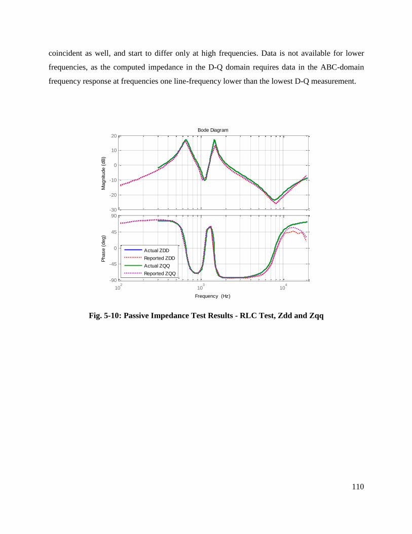
110
coincident as well, and start to differ only at high frequencies. Data is not available for lower
frequencies, as the computed impedance in the D-Q domain requires data in the ABC-domain
frequency response at frequencies one line-frequency lower than the lowest D-Q measurement.
Fig. 5-10: Passive Impedance Test Results - RLC Test, Zdd and Zqq
-30
-20
-10
0
10
20
Magnitu
de (
dB
)
102
103
104
-90
-45
0
45
90
Phase (
deg)
Bode Diagram
Frequency (Hz)
Actual ZDD
Reported ZDD
Actual ZQQ
Reported ZQQ

111
Fig. 5-11: Passive Impedance Test Results - RLC Test, Zdq and Zqd
V. Measurements which Observe Impedance of More Complex Modules
Several impedances were created to validate the operation of the converter. These
impedances were applied, and are shown in the previous section. This section demonstrates the
use of the impedance measurement unit to acquire the impedance of more complex systems,
some of which are DSP–controlled, and others of which are nonlinear. The impedance of these
systems, while it has been theorized, have not been measured in the works we‟ve found.
The following is the list of systems measured:
Unbalanced linear system
Voltage source inverter
Vienna rectifier
-60
-40
-20
0
20
Magnitu
de (
dB
)
102
103
104
-540
-360
-180
0
180
Phase (
deg)
Bode Diagram
Frequency (Hz)
Actual ZDQ
Reported ZDQ
Actual ZQD
Reported ZQD

112
Six-pulse rectifier
ATRU
It should be noted that while the impedance of the linear case is well-known and can be
derived, the impedances of the subsequent cases are not well-known, and can only be compared
to simulation models.
A. Unbalanced Conditions
We created and measured a second RLC network. The network was modified to remove the
phase C inductor, leaving all other elements present. It should be noted that this measurement
made use of the higher gain current sensors.
B. Balanced Impedance Condition
Prior to analyzing the unbalanced condition, the balanced condition for this network will be
investigated. The first step is to identify the DQ nominal impedance. This can be done from the
stationary domain using the Agilent 4394A precision impedance analyzer with the 42941A
precision impedance probe.

113
Fig. 5-12: Stationary Frame Measurements of RLC Impedance
From here, the impedance can be converted to DQ by first approximating the impedances
with a continuous state-space model, averaging the three approximations, and then performing
the stationary frame-to-D-Q transformation on the average. These derived D-Q impedances can
be seen along with the measured impedances in Fig. 5-15 and Fig. 5-16.
-20
-10
0
10
20
30
Magnitu
de (
dB
)
101
102
103
104
105
-90
-45
0
45
90
Phase (
deg)
Impedance in Stationary Coordinates
Frequency (Hz)
ZAB
ZBC
ZCA

114
Fig. 5-13: Actual Zdd and Zqq Impedances Compared to Measured Impedances
-30
-20
-10
0
10
20
Magnitu
de (
dB
)
101
102
103
104
-180
-90
0
90
180
Phase (
deg)
Balanced Case - Zdd and Zqq
Frequency (Hz)
Zdd Measured
Zqq Measured
Zdd Actual
Zqq Actual

115
Fig. 5-14: Actual and Measured Zdq and Zqd Impedances
-40
-30
-20
-10
0
10
20
Magnitu
de (
dB
)
101
102
103
104
-720
-540
-360
-180
0
180
360
Phase (
deg)
Balanced Case - Zdd and Zqq
Frequency (Hz)
Zdq Measured
Zqd Measured
Zdq Actual
Zqd Actual

116
Fig. 5-15: Actual and Filtered Zdd and Zqq Impedances
-30
-20
-10
0
10
20
Magnitu
de (
dB
)
101
102
103
104
-90
-45
0
45
90
Phase (
deg)
Balanced Case - Zdd and Zqq
Frequency (Hz)
Zdd Measured
Zqq Measured
Zdd Actual
Zqq Actual
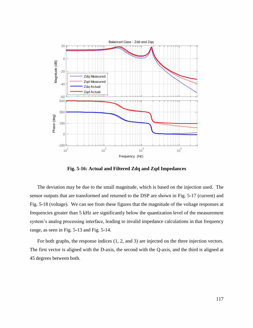
117
Fig. 5-16: Actual and Filtered Zdq and Zqd Impedances
The deviation may be due to the small magnitude, which is based on the injection used. The
sensor outputs that are transformed and returned to the DSP are shown in Fig. 5-17 (current) and
Fig. 5-18 (voltage). We can see from these figures that the magnitude of the voltage responses at
frequencies greater than 5 kHz are significantly below the quantization level of the measurement
system‟s analog processing interface, leading to invalid impedance calculations in that frequency
range, as seen in Fig. 5-13 and Fig. 5-14.
For both graphs, the response indices (1, 2, and 3) are injected on the three injection vectors.
The first vector is aligned with the D-axis, the second with the Q-axis, and the third is aligned at
45 degrees between both.
-60
-40
-20
0
20
Magnitu
de (
dB
)
101
102
103
104
-180
0
180
360
540
Phase (
deg)
Balanced Case - Zdd and Zqq
Frequency (Hz)
Zdq Measured
Zqd Measured
Zdq Actual
Zqd Actual
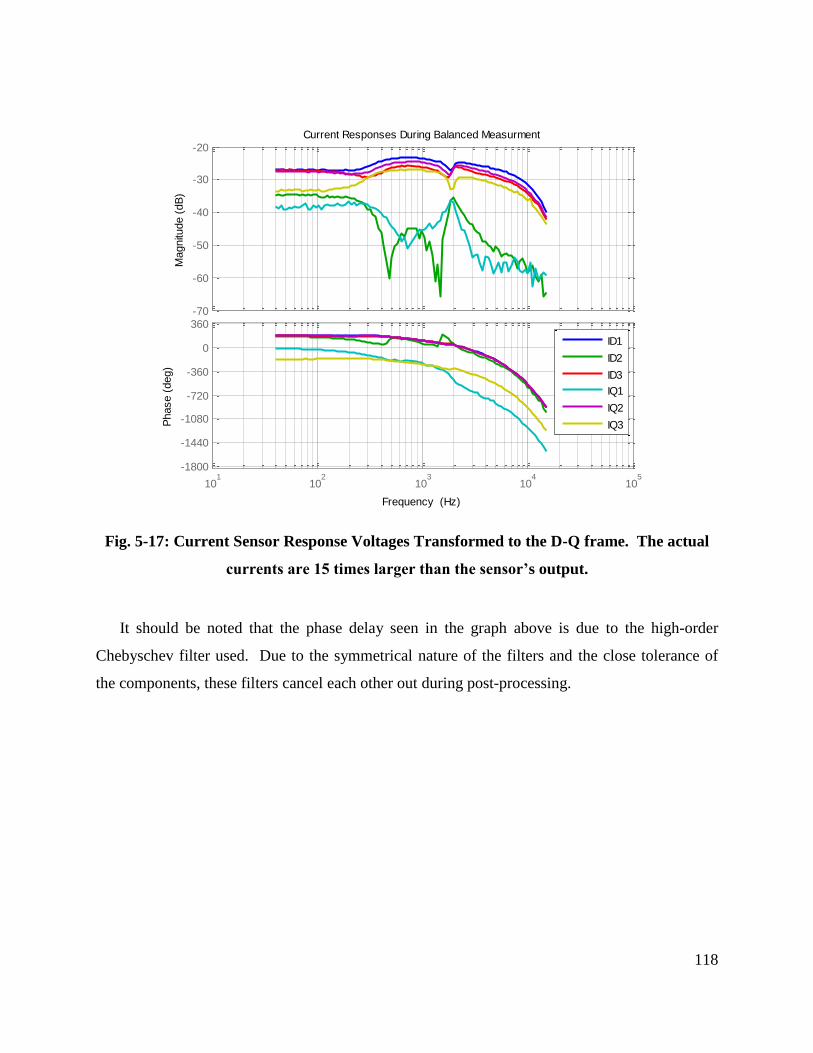
118
Fig. 5-17: Current Sensor Response Voltages Transformed to the D-Q frame. The actual
currents are 15 times larger than the sensor’s output.
It should be noted that the phase delay seen in the graph above is due to the high-order
Chebyschev filter used. Due to the symmetrical nature of the filters and the close tolerance of
the components, these filters cancel each other out during post-processing.
-70
-60
-50
-40
-30
-20
Magnitu
de (
dB
)
101
102
103
104
105
-1800
-1440
-1080
-720
-360
0
360
Phase (
deg)
Current Responses During Balanced Measurment
Frequency (Hz)
ID1
ID2
ID3
IQ1
IQ2
IQ3

119
Fig. 5-18: Load Voltage Response In To DSP Showing Significant Reduction At High
Frequencies. The actual voltages are 51 times larger than the sensor’s output.
C. Unbalanced Impedance Condition
To make the impedance significantly unbalanced, the inductor of phase C was removed from
the circuit. The new impedances can be seen in Fig. 5-19 and Fig. 5-20.
-90
-80
-70
-60
-50
-40
-30
Magnitu
de (
dB
)
101
102
103
104
105
-1440
-1080
-720
-360
0
360
Phase (
deg)
Voltage Responses During Balanced Measurment
Frequency (Hz)
VD1
VD2
VD3
VQ1
VQ2
VQ3

120
Fig. 5-19: Zdd and Zqq for Unbalanced Impedances
-30
-20
-10
0
10
20
Magnitu
de (
dB
)
101
102
103
104
-90
-45
0
45
90
Phase (
deg)
Unbalanced Case - Zdd and Zqq
Frequency (Hz)
Zdd Measured
Zqq Measured
Zdd Actual
Zqq Actual

121
Fig. 5-20: Zqd and Zdq for Unbalanced Case
VI. Switching Converters – VSI
A voltage source inverter was used as another element to test. The inverter was run from a
DC supply rated at 600 volts and 6 amps, and was run at 300 volts. The impedances were
measured in line-to-line mode, and the required neutral connection was made to the load neutral
point, although nearly no current flowed through the neutral conductor.
A. Architecture
The voltage source inverter is under current control via PI regulators with decoupling.
Additional digital filters are present in the D-Q domain. As this is a voltage-source inverter
driving a passive load, there is no need for a PLL, and the D-Q frequency of the rotation is
-60
-40
-20
0
20
Magnitu
de (
dB
)
101
102
103
104
-540
-360
-180
0
180
Phase (
deg)
Unbalanced Case - Zdd and Zqq
Frequency (Hz)
Zdq Measured
Zqd Measured
Zdq Actual
Zqd Actual

122
determined internally. The inverter was run at 3 amps RMS. The load voltage varied, depending
on the test case.
Fig. 5-21: Voltage Source Inverter Block Diagram With Control Components
B. Properties of the Nominal Impedance of the VSI
It can be shown that a VSI under current control has a rotationally invariant impedance. If
the PLL in the measurement system were misaligned in this case, the results would be the same
according to this model. The following example illustrates this:

123
Fig. 5-22: Simulated impedance of the VSI when measured with D-Q frame aligned with
the D-axis and aligned with an offset of 10 degrees from the D-Axis. The impedances are
coincident as per the model.
To properly determine the impedance of the voltage source inverter, one channel of the
inverter was left in current mode while the other channel of the inverter was left in open–loop
mode. This change made the inverter‟s impedance asymmetric, and rotating the measurement
PLL will consequently rotate the impedance. This can be shown in simulation. The following is
the impedance of the inverter when the measurement PLL is aligned with the D-axis and with the
Q-axis, showing that the impedance does vary with the measurement PLL angle. It should be
noted that there is less variation at higher frequencies because the inductor becomes the
dominant component of the converter‟s output impedance at higher frequencies.
0
50
100
From: In(1)T
o: O
ut(
1)
-180
0
180
To: O
ut(
1)
0
50
100
To: O
ut(
2)
100
105
-180
0
180
To: O
ut(
2)
From: In(2)
100
105
Bode Diagram
Frequency (Hz)
Magnitu
de (
dB
) ; P
hase (
deg)
Aligned w ith Vq=0
10 degree offset

124
Fig. 5-23: Simulated Impedances for Asymmetrical Control of the Voltage Source Inverter
Measurements of the system impedance can be used to validate the PLL alignment and
demonstrate proper operation of the PLL, as shown below:
0
20
40
From: In(1)
To: O
ut(
1)
-180
0
180
To: O
ut(
1)
0
10
20
30
To: O
ut(
2)
102
103
-180
0
180
To: O
ut(
2)
From: In(2)
102
103
Bode Diagram
Frequency (Hz)
Magnitu
de (
dB
) ; P
hase (
deg)
Aligned w ith D
Aligned w ith Q

125
Fig. 5-24: VSI Measured and Simulated Impedances: Zdd (Upper Left), Zdq (Upper
Right), Zqd (Lower Left), Zqq (Lower Right). The two simulations are two different IF
bandwidth choices. The PLL is aligned with the D-axis voltage, and the Q-axis is running
in open-loop.
It can be seen by aligning the measurement PLL with the Q-axis voltage, the impedances will
swap, making the new, rotated impedance appear as measured:
-50
0
50
From: In(1)T
o: O
ut(
1)
-180
0
180
To: O
ut(
1)
-50
0
50
To: O
ut(
2)
102
103
104
-180
0
180
To: O
ut(
2)
From: In(2)
102
103
104
Bode Diagram
Frequency (Hz)
Magnitu
de (
dB
) ; P
hase (
deg)
Simulation
TC15
TC16

126
Fig. 5-25: VSI Impedance when aligned on the Q-Axis: Zdd (Upper Left), Zdq (Upper
Right), Zqd (Lower Left), Zqq (Lower Right). The two simulations are two different IF
bandwidth choices. The PLL is aligned with the D-axis voltage, and the Q-axis is running
in open-loop.
VII. Six-Pulse Rectifier
The Vienna rectifier, when all switches are off, operates in six-pulse mode. Impedances
were taken, connecting a dynamic load to the DC side of the rectifier. With all switches in the
off position, the model can be simplified to the diagram shown in Fig. 5-26.
0
50
From: In(1)
To: O
ut(
1)
-180
0
180
To: O
ut(
1)
-50
0
50
To: O
ut(
2)
102
103
-180
0
180
To: O
ut(
2)
From: In(2)
102
103
Bode Diagram
Frequency (Hz)
Magnitu
de (
dB
) ; P
hase (
deg)

127
C
L
L
L
R
R
R
)(tvb)(tvc
)(tva
Programmable
Load
Fig. 5-26: Diode rectifier driving programmable load
The voltage source used was an HP 6834 three-phase AC power supply. The resistors used
had an impedance rated at 0.66 Ohms. The inductors had a nominal inductance of 150
microhenries. As the rectifier used the same power stage as the Vienna, the capacitance of the
DC link was split between two capacitors stacked in series, each rated at 40 microfarads,
providing a combined capacitance on the DC link of 20 microfarads. The midpoint of the
Vienna rectifier was uncontrolled during this experiment, and thus the operating point was lower
than the total rating of the Vienna rectifier to minimize overvoltage risk due to capacitor
imbalance.
We can be see from Fig. 5-27 that the current waveforms in the six-pulse rectifier are
dominated by harmonics. The current waveform is clearly non-sinusoidal, as can be seen in both
the time domain waveforms and the plane.

128
Fig. 5-27: Six-pulse rectifier waveforms showing ABC voltages in the first graticule (at 50
volts per division), ABC currents in the second graticule (at 2 amps per division), and -
currents in the third graticule (also at 2 amps per division). The fourth graticule shows the
trajectory of the current on the - plane. All waveforms vs. time are scaled to 500 S per
division.
The following figures show the results obtained for the impedance tests for the six-pulse
rectifier operating under several test conditions. The test conditions presented include constant
power loads, constant current loads and constant resistance loads on the DC bus (with an
additional capacitor present as shown in Fig. 5-26), with which two different power levels were
tested.

129
Fig. 5-28: Zdd for six-pulse rectifier showing results for constant current (CI), constant
power (CP) and constant resistance (CR) for two different power levels.
The Zdd impedance reflects the impedance of the DC link. Constant power loads on the DC
link do produce a Zdd impedance that approaches -180 degrees, as expected. Constant current
loads approach 90 degrees. This can be shown to match the impedance of the DC link capacitor.
Constant resistance loads approach zero degrees, and the constant resistance does approach 0
degrees. However, at lower frequencies, the effect of the dynamic load used dominates the
frequency response. This is also seen later with the ATRU, where the same decreasing response
was observed at low frequencies, but when replacing the dynamic load with resistors, the
response matches the DC link impedance, and does in fact go flat.
It should be noted that the constant current case impedance is invariant to power in this axis.
We will see later that the value of the capacitance and inductance can be related to the circuit.
0
10
20
30
40
50
Magnitu
de (
dB
)
101
102
103
104
105
-180
-90
0
90
Phase (
deg)
All Loads All Operating Points Zdd
Frequency (Hz)
CI 78W
CI 78W
CP 78W
CP 113W
CR 113W
CR 113W

130
Fig. 5-29: Zqq for six-pulse rectifier showing results for constant current (CI), constant
power (CP) and constant resistance (CR) for two different power levels.
As seen in Fig. 5-29, the load power influences the Zqq impedance, but the DC link
dynamics do not seem to be visible in the Zqq impedance.
25
30
35
40
45
50
Magnitu
de (
dB
)
101
102
103
104
105
-45
0
45
90
Phase (
deg)
All Loads All Operating Points Zqq
Frequency (Hz)
CI 78W
CI 78W
CP 78W
CP 113W
CR 113W
CR 113W

131
Fig. 5-30: Zdq for six-pulse rectifier showing results for constant current (CI), constant
power (CP) and constant resistance (CR) for two different power levels.
It can be seen that the Zdq impedance, as shown in Fig. 5-30, is split, and seems to be
dominated by the power level and not the DC link load type.
5
10
15
20
25
30
Magnitu
de (
dB
)
101
102
103
104
105
-45
0
45
Phase (
deg)
All Loads All Operating Points Zdq
Frequency (Hz)
CI 78W
CI 78W
CP 78W
CP 113W
CR 113W
CR 113W

132
Fig. 5-31: Zqd for six-pulse rectifier showing results for constant current (CI), constant
power (CP) and constant resistance (CR) for two different power levels
The Zqd impedance seems to have the link impedance present, although it is negative, as can
be seen by the constant current impedances cases providing impedances now approaching +90
degrees instead of -90 degrees as before, the constant power loads approaching +180 as the
frequency goes to zero, and by the constant resistance approaching zero from above. Previously
the impedances phases converged to -90 degrees, whereas here they approach +90 degrees. It
can again be seen that the frequency response is grouped in frequencies greater than 800 Hertz
by power level, and have identical phases.
5
10
15
20
25
30
Magnitu
de (
dB
)
101
102
103
104
105
-180
-90
0
90
180
Phase (
deg)
All Loads All Operating Points Zqd
Frequency (Hz)
CI 78W
CI 78W
CP 78W
CP 113W
CR 113W
CR 113W
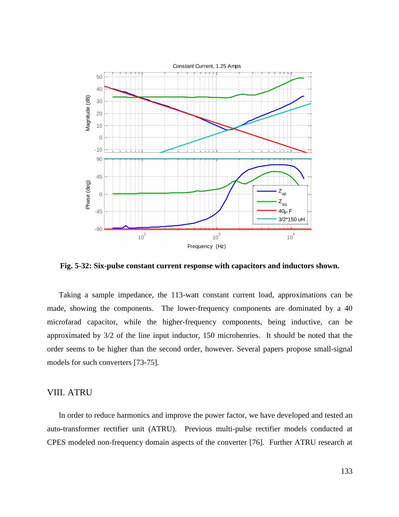
133
Fig. 5-32: Six-pulse constant current response with capacitors and inductors shown.
Taking a sample impedance, the 113-watt constant current load, approximations can be
made, showing the components. The lower-frequency components are dominated by a 40
microfarad capacitor, while the higher-frequency components, being inductive, can be
approximated by 3/2 of the line input inductor, 150 microhenries. It should be noted that the
order seems to be higher than the second order, however. Several papers propose small-signal
models for such converters [73-75].
VIII. ATRU
In order to reduce harmonics and improve the power factor, we have developed and tested an
auto-transformer rectifier unit (ATRU). Previous multi-pulse rectifier models conducted at
CPES modeled non-frequency domain aspects of the converter [76]. Further ATRU research at
-10
0
10
20
30
40
50
Magnitu
de (
dB
)
102
103
104
-90
-45
0
45
90
Phase (
deg)
Constant Current, 1.25 Amps
Frequency (Hz)
Zdd
Zqq
40 F
3/2*150 uH

134
CPES led to the production of several small-scale ATRU prototypes [77-79] including research
into the stability of systems including such converters [80].
A reduced-scale 18-pulse auto-transformer rectifier unit was tested under 700 watts of power.
The ATRU provided 151 volts on the DC side provided an input voltage of 70 volts RMS.
R
R
R
)(tvb)(tvc
)(tva
ATRU:
3 à 9 Phase
Autotransformer
(Delta-Polygon
Topology)
+ 18 Pulse
Rectifier
Electronic
Load
DCPL
DCNL
DCC
Fig. 5-33: ATRU Test setup showing source on left, followed by a source side resistor
impedance of 0.6 Ohms followed by the injection hardware followed by the ATRU and
load.
The ATRU produces a much cleaner waveform with significantly lower harmonics than the
six-pulse rectifier. The time-domain waveform is shown in Fig. 5-34.

135
Fig. 5-34: ATRU waveforms showing ABC voltages in the first graticule (at 50 volts per
division), ABC currents in the second graticlule (at 2 amps per division), and - currents
in the third graticule (also at 2 amps per division). The fourth graticule shows the
trajectory of the current on the - plane. All waveforms vs. time are scaled to 500 S per
division.

136
Fig. 5-35: ATRU Zdd showing results for constant current (CI), constant power (CP) and
constant resistance (CR) for two different power levels.
It is seen in Fig. 5-35 that the impedance does reflect the DC link, as constant power load
impedances approach -180 degrees, constant current impedances approach -90 degrees, and
constant resistance loads approach zero degrees.
-40
-20
0
20
40
Magnitu
de (
dB
)
101
102
103
104
105
-180
-90
0
90
180
Phase (
deg)
Zdd ATRU
Frequency (Hz)
CC 700W
CP 700W
CR 700W
CC 400W
CP 400W
CR 400W
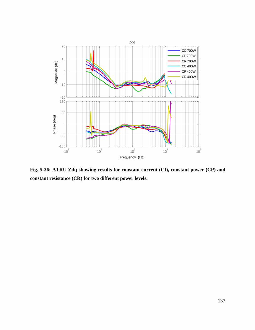
137
Fig. 5-36: ATRU Zdq showing results for constant current (CI), constant power (CP) and
constant resistance (CR) for two different power levels.
-20
-10
0
10
20
Magnitu
de (
dB
)
101
102
103
104
105
-180
-90
0
90
180
Phase (
deg)
Zdq
Frequency (Hz)
CC 700W
CP 700W
CR 700W
CC 400W
CP 400W
CR 400W
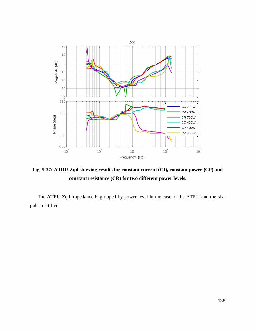
138
Fig. 5-37: ATRU Zqd showing results for constant current (CI), constant power (CP) and
constant resistance (CR) for two different power levels.
The ATRU Zqd impedance is grouped by power level in the case of the ATRU and the six-
pulse rectifier.
-40
-30
-20
-10
0
10
20
Magnitu
de (
dB
)
101
102
103
104
105
-360
-180
0
180
360
Phase (
deg)
Zqd
Frequency (Hz)
CC 700W
CP 700W
CR 700W
CC 400W
CP 400W
CR 400W

139
Fig. 5-38: ATRU Zqq showing results for constant current (CI), constant power (CP) and
constant resistance (CR) for two different power levels.
It should be noted that similar to the six-pulse rectifier, the ATRU impedances are grouped
on the Zqq axis by power level, and do not differ between different types of DC loads. The
sharp drop of the impedance near 400 Hz is suspected to be due to the dual polygon transformer
used, as it is designed for 400 Hz operation. When perturbing near 400 Hz in the DQ domain,
the ABC frame frequencies generated are near 800 Hz and near DC. The transformer was not
designed to accept frequencies lower than 400 Hz. We can see from Fig. 5-38 that the
impedance starts to drop at 400 Hz ± 200 Hz.
The low-frequency resistive characteristic is actually created based on the characteristic of an
electronic load operating in constant resistance mode. If the electronic load is substituted for an
actual resistor, more accurate results can be obtained. Fig. 5-39 is the value of the load as
measured on the DC link.
0
5
10
15
20
Magnitu
de (
dB
)
101
102
103
104
105
-90
-45
0
45
90
Phase (
deg)
Zqq
Frequency (Hz)
CC 700W
CP 700W
CR 700W
CC 400W
CP 400W
CR 400W

140
Fig. 5-39: ATRU DC Link and Zdd
This was obtained by perturbing on the D-axis via the three-phase injection system described,
while measuring the change of voltage and current on the DC side of the ATRU.
IX. Summary and Conclusions
Measurements were taken, and they agree with the model for linear loads. The operation of
the PLL is verified, and the impedances change according to PLL alignment. The VSI control
was modified to ensure the impedance was rotationally variant, forcing different impedances on
the D- and Q-axes.

141
Chapter 6. Summary and Conclusions
I. Summary
We have developed an impedance analyzer that allows its user to measure impedances in the
D-Q frame. The analyzer was an effort combining hardware- and software-based hierarchical
design, as described in Chapters 3 and 4. Several impedances were measured, as shown in
Chapter 5, and matching results were extracted for linear time-invariant impedances, while
meaningful results were extracted from switching converters–although the model used to verify
these results has not been tested sufficiently to conclude that it is correct.
A review of existing literature is provided in Chapter 1, showing that no existing solution
solves all the issues that are critical to implementing an impedance tester for three-phase
systems. While different papers have contributed different aspects, most have focused on the
injection technique, and do not address hardware implementations. Furthermore, the majority of
the papers indicate software-based simulation results, and do not show experimental results.
We have developed an impedance analyzer algorithm that includes a phase-locked loop and
an injection sequence controller. The resulting current and voltages caused by the shunt
injection of a perturbation current are captured at the load or source interface. They are then
processed after the injection using software written in Matlab scripting language. The results
may be stored and recalled for later use, as each measurement is stored along with complete
intermediate data so it may be re-processed at a later date if new techniques are made available.
Furthermore, the intermediate data serves to provide information on the accuracy of the
measurements as demonstrated.
II. Conclusion
The D-Q impedance can be measured via separate shunt current injections in the D-Q frame
by measuring the current and voltage responses to these perturbations and post-processing the
acquired data. Multiple injections are produced in the D-Q frame and are transformed to the
ABC frame where the physical injection takes place into the system. The measured currents and
142
voltages are then transformed back from the ABC domain to the D-Q domain where they are
provided to a network analyzer to acquire the system‟s response to the particular perturbation
injected. After acquiring all necessary perturbations, the system‟s impedance can be determined
via post processing the results on a per-frequency basis using the responses acquired at that
specific frequency for each angle of injection on each axis.
When acquiring these measurements, injections at certain frequencies in the D-Q domain will
cause components of the current and voltage in the stationary frame which are different. They are
the sum and difference between the injection frequency in the D-Q domain and the line
frequency. As a result, the system may be endangered if injection happens at these frequencies,
particularly injecting near the line frequency in the D-Q domain, as this will produce components
near DC in the ABC domain, leading to the risk of transformer saturation.
During the process of measurement, the D-Q frame must be aligned at a known position
relative to either the voltage or current. This was achieved in this dissertation via the use of a
phase locked loop. Furthermore, effects of PLL misalignment are shown to cause the impedance
to be different for loads whose impedance is rotationally invariant.
Results are presented indicating impedances for several passive loads, line-commutated
converters, and switching converters. The measurements are shown to be different from the
models previously developed in the D-Q domain. All impedances tested were below the 2
kilowatt level.
III. Future Work and Improvements
Testing at high power is still pending. Current testing has been limited to below two
kilowatts due to supply and load availability. Future testing at CPES can be done with linear
loads.
A. Injection Amplifiers
The models of the converters operating in the D-Q frame must be validated to ensure the
results match. It is anticipated that the current amplifiers will not be able to measure at high

143
power levels due to the small size of the current perturbation. Larger amplifiers will be required
to ensure that the amplifier can inject a sufficiently large perturbation.
B. Algorithm Implementation
The nature of the analyzer is very pipelined. Many conversions can be done in parallel. The
architecture lends itself strongly to implementation in an FPGA. Some of the filters
implemented may be implemented digitally in the FPGA using a sample rate higher than the
calculation rate. This would make them more invariant to parameter mismatches, and would
simplify the design of the analog stage of the PCB, as well as make it much easier to make
changes to the filter parameters without having to solder and remove components.
As DSP execution time is a major limiting factor in the bandwidth limitation of the system, it
would be beneficial to move as many functions as possible to the FPGA side. It is important to
consider, however, the interface chosen to partition the two processing units. Partitioning the
system at the wrong interface, one which requires the transmission of many intermediate
variables between the DSP and FPGA, may actually slow the system down due to an interface
bottleneck and limited communication bandwidth.
C. Complete real-time data flow in FPGA
If the FPGA could implement all the real-time processing functions, the bandwidth of the
system would be as fast as the time it took to execute one step. This solution utilizes a fully
pipelined architecture. Since all data travels with its corresponding data down the pipeline, there
is no relative shift of data such as current and voltage. As such, the impedance can be extracted
at a much higher rate. The pipeline latency does not affect the calculation result, as described
earlier, since all variables of interest share the same delay. The pipeline shift would be triggered
by the AD incoming sample, and the output would be synchronized with the input.
Such an implementation would not come without risks, however. A very high bit size may
be needed in order to ensure accuracy, as each operation in an FPGA typically uses fixed-point
computation, and each step would introduce quantization noise into the calculation.

144
References
[1] M. Belkhayat, R. Cooley, and E. H. Abed, "Stability and dynamics of power systems with
regulated converters," 1995 IEEE International Symposium on Circuits and Systems, Vols
1-3, pp. 143-145, 1995.
[2] M. Belkhayat, R. Cooley, and A. Witulski, "Large signal stability criteria for distributed
systems with constant power loads," Pesc 95 Record - 26th Annual IEEE Power
Electronics Specialists Conference, Vols I and II, pp. 1333-1338, 1995.
[3] M. Belkhayat, "Stability criteria for AC power systems with regulated loads," West
Lafayette, IN: Purdue University, 1997.
[4] L. Harnefors, "Modeling of three-phase dynamic systems using complex transfer functions
and transfer matrices," IEEE Transactions on Industrial Electronics, vol. 54, pp. 2239-
2248, Aug 2007.
[5] S. Chandrasekaran, D. Borojevic, and D. K. Lindner, "Input filter interaction in three phase
AC-DC converters," in Power Electronics Specialists Conference, 1999. PESC 99. 30th
Annual IEEE, 1999, pp. 987-992 vol.2.
[6] A. Emadi and M. Ehsani, "Aircraft power systems: Technology, state of the art, and future
trends," IEEE Aerospace and Electronic Systems Magazine, vol. 15, pp. 28-32, Jan 2000.
[7] J. A. Weimer, "Electrical-Power Technology for the More Electric Aircraft," Aiaa/IEEE
Digital Avionics Systems Conference, 12th Dasc, pp. 445-450, 1993.
[8] J. A. Weimer, "The role of electric machines and drives in the more electric aircraft," IEEE
Iemdc'03: IEEE International Electric Machines and Drives Conference, Vols 1-3, pp.
11-15, 2003.
[9] T. J. McCoy, "Trends in ship electric propulsion," 2002 IEEE Power Engineering Society
Summer Meeting, Vols 1-3, Conference Proceedings, pp. 343-346, 2002.
[10] N. Doerry, H. Robey, J. Amy, and C. Petry, "Powering the future with the integrated
power system," Naval Engineers Journal, vol. 108, pp. 267-279, May 1996.
[11] R. Jayabalan and B. Fahimi, "Naval shipboard power system," in Vehicle Power and
Propulsion, 2005 IEEE Conference, 2005.
[12] C. Rivetta, G. A. Williamson, and A. Emadi, "Constant power loads and negative
impedance instability in sea and undersea vehicles: Statement of the problem and
comprehensive large-signal solution," 2005 IEEE Electric Ship Technologies Symposium,
pp. 313-320, 2005.
[13] J. G. Ciezki and R. W. Ashton, "Selection and stability issues associated with a navy
shipboard DC zonal electric distribution system," IEEE Transactions on Power Delivery,
vol. 15, pp. 665-669, Apr 2000.

145
[14] A. Emadi and S. S. Williamson, "Modern Automotive Power Systems: Advancements
into the Future," in Power Electronics and Motion Control Conference, 2006. EPE-
PEMC 2006. 12th International, 2006, pp. 1762-1768.
[15] A. Emadi, A. Khaligh, C. H. Rivetta, and G. A. Williamson, "Constant power loads and
negative impedance instability in automotive systems: Definition, modeling, stability, and
control of power electronic converters and motor drives," IEEE Transactions on
Vehicular Technology, vol. 55, pp. 1112-1125, Jul 2006.
[16] A. Emadi, M. Ehsani, and J. M. Miller, Vehicular electric power systems : land, sea, air,
and space vehicles. New York: Marcel Dekker, 2004.
[17] R. G. Blakey, "Power electronics in warships," Power Engineering Journal, vol. 7, pp.
65-70, 1993.
[18] C. M. Wildrick, F. C. Lee, B. H. Cho, and B. C. Choi, "A Method of Defining the Load
Impedance Specification for a Stable Distributed Power-System," IEEE Transactions on
Power Electronics, vol. 10, pp. 280-285, May 1995.
[19] S. Rosado, R. Burgos, S. Ahmed, F. Wang, and D. Boroyevich, "Modeling of power
electronics for simulation based analysis of power systems," in Proceedings of the 2007
summer computer simulation conference San Diego, California: Society for Computer
Simulation International, 2007.
[20] G. W. Wester and R. D. Middlebrook, "Low-Frequency Characterization of Switched dc-
dc Converters," Aerospace and Electronic Systems, IEEE Transactions on, vol. AES-9,
pp. 376-385, 1973.
[21] R. W. Erickson and D. Maksimovic, Fundamentals of power electronics, 2nd ed.
Norwell, Mass.: Kluwer Academic, 2001.
[22] S. K. Mazumder, A. H. Nayfeh, and D. Boroyevich, "Theoretical and experimental
investigation of the fast- and slow-scale instabilities of a DC-DC converter," IEEE
Transactions on Power Electronics, vol. 16, pp. 201-216, Mar 2001.
[23] M. Al-Fayyoumi, "Nonlinear dynamics and interactions in power electronic systems,"
Blacksburg, VA: Virginia Polytechnic Institute and State University, 1999.
[24] S. Hiti, "Modeling and control of three-phase PWM converters," Blacksburg, VA:
Virginia Polytechnic Institute and State University, 1995., 1995.
[25] L. Harnefors, M. Bongiorno, and S. Lundberg, "Stability analysis of converter-grid
interaction using the converter input admittance," 2007 European Conference on Power
Electronics and Applications, Vols 1-10, pp. 924-933, 2007.
[26] R. Burgos, et. al, "Modeling Considerations and Stability Analysis of Aerospace Power
Systems with Hybrid AC/DC Distribution," in SAE Power Systems Conference, 2006.
[27] Y. Panov and M. Jovanovic, "Practical issues of input/output impedance measurements in
switching power supplies and application of measured data to stability analysis," Apec
2005: Twentieth Annual IEEE Applied Power Electronics Conference and Exposition,
Vols 1-3, pp. 1339-1345, 2005.
[28] M. Sumner, B. Palethorpe, and D. W. P. Thomas, "Impedance measurement for improved
power quality - Part 1: The measurement technique," IEEE Transactions on Power
Delivery, vol. 19, pp. 1442-1448, Jul 2004.
[29] M. B. Harris, A. W. Kelley, J. P. Rhode, and M. E. Baran, "Instrumentation for
Measurement of Line Impedance," Apec '94 - Ninth Annual Applied Power Electronics
Conference and Exposition, Vols 1 and 2, pp. 887-893, 1994.

146
[30] M. Sumner, B. Palethorpe, D. W. P. Thomas, P. Zanchetta, and M. C. Di Piazza, "A
technique for power supply harmonic impedance estimation using a controlled voltage
disturbance," IEEE Transactions on Power Electronics, vol. 17, pp. 207-215, Mar 2002.
[31] E. Mollerstedt and B. Bernhardsson, "Out of control because of harmonics - An analysis
of the harmonic response of an inverter locomotive," IEEE Control Systems Magazine,
vol. 20, pp. 70-81, Aug 2000.
[32] J. P. Rhode, A. W. Kelley, and M. E. Baran, "Complete characterization of utilization-
voltage power system impedance using wideband measurement," IEEE Transactions on
Industry Applications, vol. 33, pp. 1472-1479, Nov-Dec 1997.
[33] J. P. Rhode, A. W. Kelley, and M. E. Baran, "Line impedance measurement: A
nondisruptive wideband technique," Ias '95 - Conference Record of the 1995 IEEE
Industry Applications Conference/Thirtieth Ias Annual Meeting, Vols 1-3, pp. 2233-2240,
1995.
[34] A. W. Kelley and M. H. Harris, "Method and Apparatus for Nondisruptively Measuring
Line Impedance at Frequencies Which are Relatively Close to the Line Frequency," U. S.
P. a. T. Office, Ed. United States: North Carolina State University, 1995, p. 7.
[35] M. Sumner, B. Palethorpe, D. Thomas, P. Zanchetta, and M. C. Di Piazza, "Estimation of
power supply harmonic impedance using a controlled voltage disturbance," Pesc 2001:
32nd Annual Power Electronics Specialists Conference, Vols 1-4, Conference
Proceedings, pp. 522-527, 2001.
[36] M. C. Di Piazza, P. Zanchetta, M. Sumner, and D. W. P. Thomas, "Estimation of load
impedance in a power system," Ninth International Conference on Harmonics and
Quality of Power Proceedings, Vols I - Iii, pp. 520-525, 2000.
[37] B. Palethorpe, M. Sumner, and D. W. P. Thomas, "System impedance measurement for
use with active filter control," Eighth International Conference on Power Electronics and
Variable Speed Drives, pp. 24-28, 2000.
[38] B. Palethorpe, M. Sumner, and D. W. P. Thomas, "Power system impedance
measurement using a power electronic converter," Ninth International Conference on
Harmonics and Quality of Power Proceedings, Vols I - Iii, pp. 208-213, 2000.
[39] S. D. Sudhoff, B. P. Loop, J. Byoun, and A. M. Cramer, "A new procedure for
calculating immittance characteristics using detailed computer simulations," 2007 IEEE
Power Electronics Specialists Conference, Vols 1-6, pp. 901-908, 2007.
[40] Y. Familiant, "AC impedance measurement techniques in power systems," in Electrical
Engineering Milwaukee: University of Wisconsin - Milwaukee, 2006, p. 115.
[41] Y. L. Familiant, K. A. Corzine, J. Huang, and M. Belkhayat, "AC Impedance
Measurement Techniques," in Electric Machines and Drives, 2005 IEEE International
Conference on, 2005, pp. 1850-1857.
[42] J. Huang, K. A. Corzine, and M. Belkhayat, "Small-Signal Impedance Measurement of
Power-Electronics-Based AC Power Systems Using Line-to-Line Current Injection,"
IEEE Transactions on Power Electronics, vol. 24, pp. 445-455, Jan-Feb 2009.
[43] M. Belkhayat, "Impedance Measurement Using Line-To-Line Current Injection," U.S.,
Ed. United States, 2008.
[44] H. Zhu, in Electrical Engineering. vol. Ph. D. Blacksburg: Virginia Polytechnic Institute
and State University, 2005.
147
[45] J. T. Boys and P. G. Handley, "Harmonic analysis of space vector modulated PWM
waveforms," Electric Power Applications, IEE Proceedings B, vol. 137, pp. 197-204,
1990.
[46] S. F. A. Mehrizi-Sani, and P. L. Wilson, "Harmonic and Loss Analysis of Space-Vector
Modulated Converters," in International Conference on Power Systems Transients
(IPST'07) Lyon, France, 2007.
[47] S. Jian, "On the zero-crossing distortion in single-phase PFC converters," Power
Electronics, IEEE Transactions on, vol. 19, pp. 685-692, 2004.
[48] K. J. Karimi and A. C. Mong, "Modeling nonlinear loads for aerospace power systems,"
in Energy Conversion Engineering Conference, 2002. IECEC '02. 2002 37th Intersociety,
2002, pp. 33-38.
[49] S. Jian, C. Min, and K. J. Karimi, "Aircraft power system harmonics involving single-
phase PFC converters," Aerospace and Electronic Systems, IEEE Transactions on, vol.
44, pp. 217-226, 2008.
[50] R. S. Zhang, "High performance power converter systems for nonlinear and unbalanced
load/source," [Blacksburg, Va.: University Libraries, Virginia Polytechnic Institute and
State University, 1998.
[51] P. Rodriguez, J. Pon, J. Bergas, J. I. Candela, R. P. Burgos, and D. Boroyevich,
"Decoupled double synchronous reference frame PLL for power converters control (vol
22, pg 584, 2007)," IEEE Transactions on Power Electronics, vol. 22, pp. 1078-1078,
May 2007.
[52] J. Huang, K. Corzine, and M. Belkhayat, "Single-phase ac impedance modeling for
stability of integrated power systems," 2007 IEEE Electric Ship Technologies
Symposium, pp. 483-489, 2007.
[53] S. Cobreces, F. Huerta, D. Pizarro, F. J. Rodrguez, and E. J. Bueno, "Three-phase power
system parametric identification based on complex-space recursive least squares," 2007
IEEE International Symposium on Intelligent Signal Processing, Conference Proceedings
Book, pp. 563-568, 2007.
[54] P. Xiao, G. K. Venayagamoorthy, and K. A. Corzine, "Combined training of recurrent
neural networks with particle swarm optimization and backpropagation algorithms for
impedance identification," 2007 IEEE Swarm Intelligence Symposium, pp. 9-15, 2007.
[55] P. Xiao, G. K. Venayagamoorthy, and K. A. Corzine, "Impedance identification of
integrated power system components using recurrent neural networks," 2007 IEEE
Electric Ship Technologies Symposium, pp. 48-52, 2007.
[56] P. Xiao, G. Venayagamoorthy, and K. Corzine, "A novel impedance measurement
technique for power electronic systems," 2007 IEEE Power Electronics Specialists
Conference, Vols 1-6, pp. 955-960, 2007.
[57] V. Kaura and V. Blasko, "Operation of a phase locked loop system under distorted utility
conditions," IEEE Transactions on Industry Applications, vol. 33, pp. 58-63, Jan-Feb
1997.
[58] P. Rodriguez, J. Pou, J. Bergas, J. I. Candela, R. P. Burgos, and D. Boroyevich,
"Decoupled double synchronous reference frame PLL for power converters control,"
IEEE Transactions on Power Electronics, vol. 22, pp. 584-592, Mar 2007.
[59] H. W. Johnson and M. Graham, High-speed digital design : a handbook of black magic.
Englewood Cliffs, N.J.: Prentice Hall, 1993.
148
[60] C. C. Xiao, L. Y. Zhao, T. Asada, W. G. Odendaal, and J. D. van Wyk, "An overview of
integratable current sensor technologies," 2003 IEEE Industry Applications Conference,
Vols 1-3, pp. 1251-1258, 2003.
[61] G. Francis, "A synchronous distributed digital control architecture for high power
converters," [Blacksburg, Va.: University Libraries, Virginia Polytechnic Institute and
State University, 2004.
[62] G. Francis, R. Burgos, P. Rodriguez, F. Wang, D. Boroyevich, R. Liu, and A. Monti,
"Virtual prototyping of universal control architecture systems by means of processor in
the loop technology," Apec 2007: Twenty-Second Annual IEEE Applied Power
Electronics Conference and Exposition, Vols 1 and 2, pp. 21-27, 2007.
[63] G. Francis, R. Burgos, F. Wang, and D. Boroyevich, "A universal controller for
distributed control of power electronics conversion systems," Proceedings of the 2006
IEEE Workshop on Computers in Power Electronics, pp. 8-14, 2006.
[64] G. W. Francis, R. P. Burgos, I. Celanovic, F. Wang, and D. Boroyevich, "A universal
controller for distributed control of power electronics systems in electric ships," ACC:
Proceedings of the 2005 American Control Conference, Vols 1-7, pp. 1999-2004, 2005.
[65] R. Liu, A. Monti, G. Francis, R. Burgos, F. Wang, and D. Boroyevich, "Implementing a
processor-in-the-loop with a universal controller in the virtual test bed," 2007 IEEE
Power Electronics Specialists Conference, Vols 1-6, pp. 945-950, 2007.
[66] R. P. Burgos, P. Kshirsagar, A. Lidozzi, H. Jang, F. Wang, D. Boroyevich, P. Rodriguez,
and S. K. Sul, "Design and evaluation of a PLL-based position controller for sensorless
vector control of permanent-magnet synchronous machines," Iecon 2006 - 32nd Annual
Conference on IEEE Industrial Electronics, Vols 1-11, pp. 5196-5201, 2006.
[67] D. Ghizoni, R. Burgos, G. Francis, J. Guo, X. Ma, L. Solero, F. Wang, D. Boroyevich,
and D. A. Cartes, "Design and evaluation of a 33 kW PEBB module for distributed power
electronics conversion systems," 2005 IEEE 36th Power Electronic Specialists
Conference (PESC), Vols 1-3, pp. 530-536, 2005.
[68] A. D. Inc, "AD7656-1: 250 kSPS, 6-Channel, Simultaneous Sampling, Bipolar 16-Bit
ADC."
[69] T. U. I. Forum, "USB 2.0 Specification."
[70] J. R. Armstrong and F. G. Gray, Structured logic design with VHDL. Englewood Cliffs,
N.J.: PTR Prentice Hall, 1993.
[71] D. Rogerson, Inside COM. Redmond, Wash.: Microsoft Press, 1997.
[72] J. Richter, Advanced Windows, 3rd ed. Redmond, Wash.: Microsoft Press, 1997.
[73] B. Zhonghui, K. J. Karimi, and S. Jian, "Input Impedance Modeling and Analysis of
Line-Commutated Rectifiers," in Power Electronics Specialists Conference, 2007. PESC
2007. IEEE, 2007, pp. 1981-1987.
[74] S. Jian and K. J. Karimi, "Small-signal input impedance modeling of line-frequency
rectifiers," Aerospace and Electronic Systems, IEEE Transactions on, vol. 44, pp. 1489-
1497, 2008.
[75] S. Jian and J. Colon, "Input Impedance Modeling of Line-Frequency Rectifiers by the
Method of Impedance Mapping," in Computers in Power Electronics, 2006. COMPEL
'06. IEEE Workshops on, 2006, pp. 69-75.
[76] C. T. Tinsley, "Modeling of multi-pulse transformer/rectifier units in power distribution
systems," [Blacksburg, Va.: University Libraries, Virginia Polytechnic Institute and
State University, 2003.

149
[77] S. Rosado, R. Burgos, F. Wang, and D. Boroyevich, "Large- and Small-Signal Evaluation
of Average Models for Multi-Pulse Diode Rectifiers," in Computers in Power
Electronics, 2006. COMPEL '06. IEEE Workshops on, 2006, pp. 89-94.
[78] H. Zhu, "New multi-phase diode rectifier average models for AC and DC power system
studies," [Blacksburg, Va.: University Libraries, Virginia Polytechnic Institute and State
University, 2005.
[79] A. Uan-Zo-li, R. Burgos, F. Wang, D. Boroyevich, F. Lacaux, and A. Tardy,
"Comparison of prospective topologies for aircraft autotransformer-rectifier units," in
Industrial Electronics Society, 2003. IECON '03. The 29th Annual Conference of the
IEEE, 2003, pp. 1122-1127 Vol.2.
[80] S. Rosado, R. Burgos, F. Wang, and D. Boroyevich, "Large-Signal Stability Assessment
of AC/DC Systems with Multi-Pulse Rectification and DC-Fed PWM Motor Drives," in
Power Electronics Specialists Conference, 2007. PESC 2007. IEEE, 2007, pp. 2168-
2173.


![Enhance High Impedance Fault Detection and …yweng2/papers/2019TSG-PMU.pdfalgorithm [2], impedance-based method [3] and PC-based fault locating and diagnosis algorithm [4], etc. However,](https://static.fdocuments.us/doc/165x107/5fe122d4df236711b2274e10/enhance-high-impedance-fault-detection-and-yweng2papers2019tsg-pmupdf-algorithm.jpg)


![The Observer Algorithm for Visibility Approximation · can be done for example using Bresenham’s circle algorithm [9] which is used here. The circle algorithm calculates the coordinates](https://static.fdocuments.us/doc/165x107/601615fe2510ed5a9d603fe2/the-observer-algorithm-for-visibility-approximation-can-be-done-for-example-using.jpg)
