An accurate prediction of high-frequency circuit … accurate prediction of high-frequency circuit...
16
Invited paper An accurate prediction of high-frequency circuit behaviour Sadayuki Yoshitomi, Hideki Kimijima, Kenji Kojima, and Hideyuki Kokatsu Abstract—An accurate way to predict the behaviour of an RF analogue circuit is presented. A lot of effort is required to eliminate the inaccuracies that may generate the devia- tion between simulation and measurement. Efficient use of computer-aided design and incorporation of as many physical effects as possible overcomes this problem. Improvement of transistor modelling is essential, but there are many other un- solved problems affecting the accuracy of RF analogue circuit modelling. In this paper, the way of selection of accurate tran- sistor model and the extraction of parasitic elements from the physical layout, as well as implementation to the circuit sim- ulation will be presented using two CMOS circuit examples: an amplifier and a voltage controlled oscillator (VCO). New simulation technique, electro-magnetic (EM)-co-simulation is introduced. Keywords—electro-magnetic simulation, SPICE, circuit test structure, RF CMOS, EKV2.6-MOS model, spiral inductor, CMOS VCO. 1. Introduction The goal of RF analogue circuit design with ultimate accuracy has been sought by both modelling and circuit engineers for a long time. The necessity to consider the electro-magnetic (EM) effects has been recognized because the electro-magnetic behaviour of the signal line and the passive elements can have considerable effect on the cir- cuit performance. The following phenomena become prominent: the self- inductance, skin effect and mutual electrical coupling be- tween signal lines and the electro-magnetic loss of silicon substrate. These factors are as important for the design as for the accuracy of the transistor SPICE model. Moreover, the issue becomes even more critical as the operating fre- quency of RF circuits is increased. Introduction of the above phenomena into the model is not easy because of their dependence on the type of the layout, location, size of the device, the number and the structural configuration of the transistor, etc. Thus, for the circuit design of chips intended for mass production, the electro- magnetic behaviour has still not been introduced until today. In this paper, ways to overcome this problem for the semi- conductor industry have been proposed. This is a new sim- ulation technique, EM-co-simulation [1]. The main idea is to share the results of EM simulation with the circuit simulation. Each step, as well as the results of the verification will be explained in this paper. All the test structures presented in this paper have been fabricated in TOSHIBA’s 3.3 V, 0.40 μ m rule SiGe BiC- MOS technology. The maximum values of f T and f max of n-p-n transistors are 30 GHz and 50 GHz, respectively, and the maximum f T of NMOS is about 20 GHz. Three metal layers have been implemented with the uppermost layer of 3 μ m thickness dedicated for the fabrication of inductors. This report consists of the following parts: – selection of CMOS SPICE model, – investigation of the applicability of EM simulation, – verification of the circuit performance by using EM- co-simulation technique. 2. Selection of CMOS SPICE model An accurate transistor model is the most essential matter for the real circuit design. Lately, surface potential (SP) based MOS models, such as EKV [3–5], HiSIM [6] and SP [7] have become well recognized. Among these three models, only EKV Version 2.6 (EKV2.6) has already been implemented into several commercial-based simulators, therefore, a comparison in terms of DC and small signal output characteristics be- tween EKV 2.6 and BSIM3 Version 3.2 (BSIM3V3.2) [8, 9] was made. 2.1. Device measurement and stability test Before starting the discussion on the accuracy of the above two models, one should rather clear the measurement sta- bility issue first to make the discussion trustworthy. Its solution is to analyze the robustness of the measurement data by using statistical approach. The detailed procedure will be explained in the following section. The measurement of MOS transistors with three geome- tries: large (L g = 10 μ m, W g = 10 μ m), short (L g = 0.4 μ m, W g = 10 μ m), and narrow (L g = 10 μ m, W g = 0.6 μ m), has been performed by two persons for 4 chips belonging to one wafer. This 8 (= 4 times 2) sets of measurements have been repeated three times. A total of 24 measurement data for each size have been collected. Agilent’s HP4156 with cascade probe station has been used as a measurement tool. 47
Transcript of An accurate prediction of high-frequency circuit … accurate prediction of high-frequency circuit...

Invited paper An accurate prediction
of high-frequency circuit behaviour
Sadayuki Yoshitomi, Hideki Kimijima, Kenji Kojima, and Hideyuki Kokatsu
Abstract—An accurate way to predict the behaviour of an
RF analogue circuit is presented. A lot of effort is required
to eliminate the inaccuracies that may generate the devia-
tion between simulation and measurement. Efficient use of
computer-aided design and incorporation of as many physical
effects as possible overcomes this problem. Improvement of
transistor modelling is essential, but there are many other un-
solved problems affecting the accuracy of RF analogue circuit
modelling. In this paper, the way of selection of accurate tran-
sistor model and the extraction of parasitic elements from the
physical layout, as well as implementation to the circuit sim-
ulation will be presented using two CMOS circuit examples:
an amplifier and a voltage controlled oscillator (VCO). New
simulation technique, electro-magnetic (EM)-co-simulation is
introduced.
Keywords—electro-magnetic simulation, SPICE, circuit test
structure, RF CMOS, EKV2.6-MOS model, spiral inductor,
CMOS VCO.
1. Introduction
The goal of RF analogue circuit design with ultimate
accuracy has been sought by both modelling and circuit
engineers for a long time. The necessity to consider the
electro-magnetic (EM) effects has been recognized because
the electro-magnetic behaviour of the signal line and the
passive elements can have considerable effect on the cir-
cuit performance.
The following phenomena become prominent: the self-
inductance, skin effect and mutual electrical coupling be-
tween signal lines and the electro-magnetic loss of silicon
substrate. These factors are as important for the design as
for the accuracy of the transistor SPICE model. Moreover,
the issue becomes even more critical as the operating fre-
quency of RF circuits is increased.
Introduction of the above phenomena into the model is not
easy because of their dependence on the type of the layout,
location, size of the device, the number and the structural
configuration of the transistor, etc. Thus, for the circuit
design of chips intended for mass production, the electro-
magnetic behaviour has still not been introduced until today.
In this paper, ways to overcome this problem for the semi-
conductor industry have been proposed. This is a new sim-
ulation technique, EM-co-simulation [1].
The main idea is to share the results of EM simulation with
the circuit simulation. Each step, as well as the results of
the verification will be explained in this paper.
All the test structures presented in this paper have been
fabricated in TOSHIBA’s 3.3 V, 0.40 µm rule SiGe BiC-
MOS technology. The maximum values of fT and fmaxof n-p-n transistors are 30 GHz and 50 GHz, respectively,
and the maximum fT of NMOS is about 20 GHz. Three
metal layers have been implemented with the uppermost
layer of 3 µm thickness dedicated for the fabrication of
inductors.
This report consists of the following parts:
– selection of CMOS SPICE model,
– investigation of the applicability of EM simulation,
– verification of the circuit performance by using EM-
co-simulation technique.
2. Selection of CMOS SPICE model
An accurate transistor model is the most essential matter
for the real circuit design. Lately, surface potential (SP)
based MOS models, such as EKV [3–5], HiSIM [6] and
SP [7] have become well recognized.
Among these three models, only EKV Version 2.6
(EKV2.6) has already been implemented into several
commercial-based simulators, therefore, a comparison in
terms of DC and small signal output characteristics be-
tween EKV 2.6 and BSIM3 Version 3.2 (BSIM3V3.2) [8, 9]
was made.
2.1. Device measurement and stability test
Before starting the discussion on the accuracy of the above
two models, one should rather clear the measurement sta-
bility issue first to make the discussion trustworthy. Its
solution is to analyze the robustness of the measurement
data by using statistical approach. The detailed procedure
will be explained in the following section.
The measurement of MOS transistors with three geome-
tries: large (Lg = 10 µm, Wg = 10 µm), short (Lg = 0.4 µm,
Wg = 10 µm), and narrow (Lg = 10 µm, Wg = 0.6 µm),
has been performed by two persons for 4 chips belonging
to one wafer. This 8 (= 4 times 2) sets of measurements
have been repeated three times. A total of 24 measurement
data for each size have been collected. Agilent’s HP4156
with cascade probe station has been used as a measurement
tool.
47

Sadayuki Yoshitomi, Hideki Kimijima, Kenji Kojima, and Hideyuki Kokatsu
To evaluate the model’s accuracy two quantities Dev gmsand Dev n f act have been introduced defined by the follow-
ing formulae:
Dev gms = ∑large,short,narrow
IDIspec =10
∑ID
Ispec =0.1
|meas(gms)−sim(gms)|sim(gms)
,
(1)
Dev n fact = ∑large,short,narrow
IDIspec =10
∑ID
Ispec =0.1
|meas(n)− sim(n)|sim(n)
. (2)
The measurement and calculation of gms (normalized gate-
to-source conductance) and n (slope factor) have been done
using formulae (3)–(9), where ID is the drain current, UT is
the thermal voltage (= kT/q), q is the electron charge,
εsi is the silicon permittivity, Nsub is the doping concen-
tration in silicon, and VTO is the threshold voltage.
Using (4), the universal function Gs expressed by (3) [5]
can be obtained from the gms, that can easily be obtained
from the simulation and measurement data. In this sense,
Gs is a useful figure, because both simulated and measured
behaviour of a MOSFET should follow this function:
GS =1
12
+
√
14
+ID
Ispec
, (3)
gms ≡ −∂ ID
∂VS
∣
∣
∣
∣
VG,VD
=GS · ID
UT, (4)
where:
Ispec = 2 ·n ·U2T ·µ ·Cox ·
WL
, (5)
n ≡[
∂VP
∂VG
]−1
= 1+GAMMA
2√
Ψo +VP, (6)
where:
VP ∼= VG −VTO
n, (7)
GAMMA =√
2qεsiNsub/
C′ox , (8)
Ψ0 = 2 ·UT · ln(
Nsub/ni)
. (9)
The Dev gms and Dev n fact have been calculated and sta-
tistical analysis has been performed with Minitab [10]
software using the obtained data. Figures 1 and 2 show
the statistical distribution of Dev gms and Dev n fact and
Fig. 1. Run chart of Dev gms and Dev n fact in the case of
EKV2.6 model.
Fig. 2. Statistical distribution of Dev gms and Dev n fact values
in the case of EKV2.6 model.
48

An accurate prediction of high-frequency circuit behaviour
Table 1 summarizes the analytical result. Gauge R&R in
Table 1 is the measure of the stability of the measurement
system, which is the total sum of % contribution of three
factors: (1) repeatability, (2) reproductivity and (3) mea-
surement operator. The theory requires that Gauge R&R
should be less than 20% [10].
Table 1
Summary of the stability test of Dev gms and Dev n factin case of EKV2.6 model
Factor Contribution [%]
for robustness Dev gms Dev n fact
Total Gauge R&R 5.49 13.12
– repeatability 5.49 13.12
– reproductivity 0 0
– fellow 0 0
Part-to-part 94.51 86.88
Total variation 100 100
The resultant Dev n fact and Dev gms value in Table 1 was
5.49% and 13.2% respectively, which is less than 20%.
It has been concluded that the way of measurement used
in this study is stable and independent of the measure-
ment operator so that the obtained measurement data is
trustworthy.
2.2. Results and discussion of the benchmark test
The SPICE parameter extraction for EKV2.6 and
BSIM3V3.2 models was done. The number of model
parameters was 26 in the case of extraction based on
EKV2.6 (including 22 original parameters and 4 pa-
rameters for extrinsic elements) and 81 in the case of
BSIM3V3.2 (all 81 original parameters). Simulation data
has been generated by Synopsys’s HSPICE2002.2. Agi-
lent’s ICCAP has been used for verification and parameter
extraction.
It should be noted that the parameters of both mod-
els include the temperature effects in the range from
−40C to 150C. The number of the variations of geo-
metrical test patterns used for the extraction is 19 (gate
length ranges from 0.35 µm to 10 µm, and gate width
from 0.6 µm to 10 µm).
After parameter extraction, simulation data was generated
to calculate Dev gms and Dev n fact , and the median value of
24 samples for each model was obtained using the Minitab
software. Discussion on the modelling accuracy has been
done based on this median value.
Figure 3 shows the comparison of Gs between EKV2.6 and
BSIM3V3.2 for short and large devices. One should focus
Fig. 3. The benchmark result of Gs(= gmsUT /ID) according to
EKV2.6 and BSIM3V3.2 for: (a) short device (Ispec = 3.0 µA);
(b) large device (Ispec = 280 nA).
on the Gs value in the range 0.1 < ID/Ispec < 10, which
corresponds to the operation region of MOSFET between
moderate and strong inversion, which is typically used for
analogue circuits. This figure shows that both theoretical
and measured Gs values match well. This means that the
formula (3) is a valid expression for MOSFETs output char-
acteristics.
As for the simulated results between two models, the
EKV2.6 model is a better fit with Gs than BSIM3V3.2 in
the whole range of ID/Ispec. This fact indicates that EKV2.6
can describe the real behaviour of MOSFETs much better
than BSIM3V3.2.
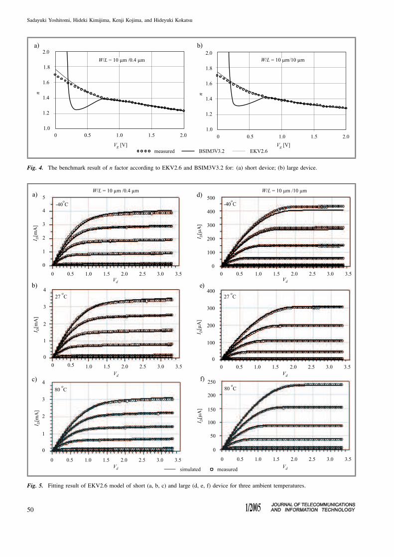
Comparison of the slope factor n has been performed and
the results are given in Fig. 4. Strange behaviour has
been observed in the case of BSIM3V3.2 results. The
BSIM3V3.2 curve started decreasing for voltages below
VGB = 0.7 V and then increasing sharply for VGB more
49
Sadayuki Yoshitomi, Hideki Kimijima, Kenji Kojima, and Hideyuki Kokatsu
Fig. 4. The benchmark result of n factor according to EKV2.6 and BSIM3V3.2 for: (a) short device; (b) large device.
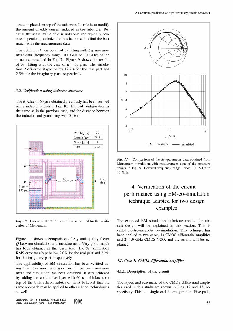
Fig. 5. Fitting result of EKV2.6 model of short (a, b, c) and large (d, e, f) device for three ambient temperatures.
50

An accurate prediction of high-frequency circuit behaviour
closer to 0, while the EKV2.6 curve is in good agreement
with the measured data.
The results are summarized in Table 2. Dev gms for
EKV2.6 was 21.0, which is approximately 1/5 of that of
BSIM3V3.2 (99.0). The same holds for Dev n fact which
was only 2.10 for EKV2.6, while it rose to 28.3 for
BSIM3V3.2, which is 13.5 times higher. This confirms that
EKV2.6 is better to use than BSIM3V3.2. These results
coincide completely with those presented by Dr. Matthias
Bucher [5].
Table 2
Comparison of Dev gms and Dev n fact values
calculated according to EKV2.6 and BSIM3V3.2
Contents EKV2.6 BSIM3V3.2
Dev gms 21.0 99.0
Dev n fact 2.10 28.3
Figure 5 shows the results of the verification of EKV2.6
models over three ambient temperatures (−40C, 27Cand 80C). It is amazing that this superb fit could be
obtained using only 26 model parameters.
As a result of the above investigation, EKV2.6 was chosen
for the entire study in this research.
2.3. Modification of the MOSFET SPICE model
for RF application
In the previous section, the modelling accuracy of the
intrinsic part of MOSFET has been discussed. However,
the following extrinsic elements should be taken in account
in the case of high frequency circuit operation:
1. Ohmic resistance of the gate material.
2. Resistance between source or drain and the substrate.
3. Coupling capacitances between gate, drain and
source, respectively.
Figure 6 shows the EKV2.6 model modified for RF appli-
cation [11–14]. Two added resistors RG and RB describe
the gate and substrate resistance, respectively. Two capac-
itances (CGDFI and CGSFI) placed between the gate and
drain, and gate and source are the sum of the overlap ca-
pacitances for the intrinsic part (CGD and CGS) and the ex-
trinsic part describing the coupling between gate and drain,
and gate and source electrodes (CGD FI and CGS FI) .
These values have been related to the physical layout by
the following formulae [13, 14]. In the following sec-
tion, extraction procedure of these values will be explained
later.
- - - Device configuration - - -
Lg [m] : gate length
W f [m] : finger length
Multi : numbers of parallel devices
RPSH [Ω/square] : sheet resistance of gate material
RGCT [Ω] : gate contact resistance
- - - Gate resistance reduction factor - - -
FRG = 13 (one sided) (10)
FRG = 112 (double sided) (11)
- - - Formula for the extraction of RG - - -
RGSH = RPSH ·FRG (12)
RG =RGCT +RGSH ·W f /Lg
Multi (13)
- - - Formula for the extraction of RB- - -
Rbre f : RB value used for best fit
W f re f : finger length used to fit RB
RB =Rbre fW fre f
W f Multi(14)
- - - G-D coupling capacitance - - -
CGDFI = (CGD +CGD FI)W f Multi (15)
- - - G-S coupling capacitance - - -
CGSFI = (CGS +CGS FI)W f Multi (16)
Fig. 6. Subcircuit-based EKV2.6 model with W f (finger
length) = 20 µm, Lg (gate length) = 0.4 µm, and Multi (numbers
of fingers) = 5.
51

Sadayuki Yoshitomi, Hideki Kimijima, Kenji Kojima, and Hideyuki Kokatsu
3. Investigation of the applicability
of EM simulation
In this section, the results of the investigation of the ap-
plicability of electro-magnetic simulation will be explained
using pad and inductor structures. Agilent’s Momentum [1]
has been used as a simulation tool.
3.1. Verification using pad structure
Figure 7 is the layout view of the pad structure used as the
first case of the investigation. This is 1 port ground (G)-
signal (S)-ground (G) configuration with 150 µm pitch.
Fig. 7. Layout of the pad structure used for the verification of
Momentum.
Fig. 8. Cross sectional information on TOSHIBA’s 0.4 µm
BiCMOS technology used for Momentum simulation.
Two G pads are connected to the silicon substrate through
guard ring. Figure 8 illustrates the cross sectional infor-
mation on the BiCMOS process used for the Momentum
simulation. A thin conductive layer with variable thick-
ness (d), which has the same resistivity as the bulk sub-
Fig. 9. Comparison of the S11-parameter data obtained from
Momentum simulation with measurement data of the structure
shown in Fig. 8. Covered frequency range: from 100 MHz to
10 GHz.
52
An accurate prediction of high-frequency circuit behaviour
strate, is placed on top of the substrate. Its role is to modify
the amount of eddy current induced in the substrate. Be-
cause the actual value of d is unknown and typically pro-
cess dependent, optimization has been used to find the best
match with the measurement data.
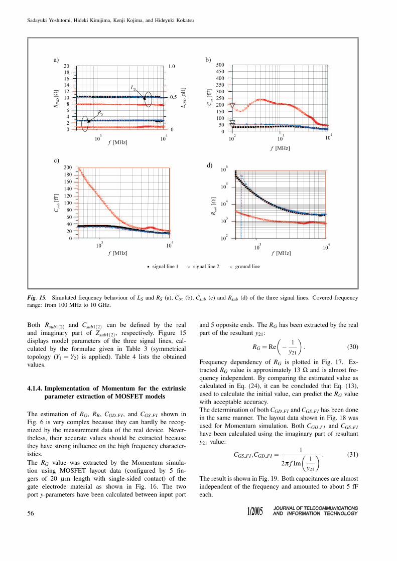
The optimum d was obtained by fitting with S11 measure-
ment data (frequency range: 0.1 GHz to 10 GHz) of the
structure presented in Fig. 7. Figure 9 shows the results
of S11 fitting with the case of d = 60 µm. The simula-
tion RMS error stayed below 12.2% for the real part and
2.5% for the imaginary part, respectively.
3.2. Verification using inductor structure
The d value of 60 µm obtained previously has been verified
using inductor shown in Fig. 10. The pad configuration is
the same as in the previous case, and the distance between
the inductor and guard-ring was 20 µm.
Fig. 10. Layout of the 2.25 turns of inductor used for the verifi-
cation of Momentum.
Figure 11 shows a comparison of S11 and quality factor
Q between simulation and measurement. Very good match
has been obtained in this case, too. The S11 simulation
RMS error was kept below 2.0% for the real part and 2.2%
for the imaginary part, respectively.
The applicability of EM simulation has been verified us-
ing two structures, and good match between measure-
ment and simulation has been obtained. It was achieved
by adding the conductive layer with 60 µm thickness on
top of the bulk silicon substrate. It is believed that the
same approach may be applied to other silicon technologies
as well.
Fig. 11. Comparison of the S11-parameter data obtained from
Momentum simulation with measurement data of the structure
shown in Fig. 8. Covered frequency range: from 100 MHz to
10 GHz.
4. Verification of the circuit
performance using EM-co-simulation
technique adapted for two design
examples
The extended EM simulation technique applied for cir-
cuit design will be explained in this section. This is
called electro-magnetic co-simulation. This technique has
been applied to two cases, 1) CMOS differential amplifier
and 2) 1.9 GHz CMOS VCO, and the results will be ex-
plained.
4.1. Case 1: CMOS differential amplifier
4.1.1. Description of the circuit
The layout and schematic of the CMOS differential ampli-
fier used in this study are shown in Figs. 12 and 13, re-
spectively. This is a single-ended configuration. Five pads,
53

Sadayuki Yoshitomi, Hideki Kimijima, Kenji Kojima, and Hideyuki Kokatsu
located on the upper side of the circuit are for the DC
power supply, and two sets of G-S-G pads on both sides
are provided for the input/output. This circuit, which is
fully dedicated for the verification of model parameters,
has the following features.
1. Unified device configuration to suppress the pro-
cess fluctuation effect.
All transistors in the circuit are NMOSFETs with the
following geometry and configuration of RG:
Lg (gate length) = 0.4 µm, (17)
W f (finger length) = 20 µm, (18)
Multi (numbers of parallel devices) = 5, (19)
FRG = 13 (single-sided gate contact), (20)
RPSH (sheet resistance of gate
material) = 3.5 Ω/square, (21)
RGCT (gate contact resistance) = 3 Ω, (22)
RGSH = RPSH ·FRG = 1.67 Ω/square, (23)
RG =RGCT +RGSH ·W f /Lg
Multi= 12.3 Ω. (24)
All resistors are used with a series or parallel connec-
tion of the 300 Ω resistor having 4 µm width. This is
aimed at reducing the effect of process fluctuations,
which strongly depends on the resistor width.
2. Only 1st and 2nd metal layers have been used.
This is for practical reasons. A shorter turn-around
time was expected.
3. Special pattern has been fabricated to calibrate
out the parasitic impedances of the pads.
Open calibration pattern was prepared to detect the
intrinsic behaviour of the circuit.
Fig. 12. Layout of CMOS differential amplifier.
Fig. 13. Schematics of CMOS differential amplifier shown in
Fig. 12.
4.1.2. Conditions of the measurement and simulation
The two port S-parameter measurement was done in the
following conditions:
– frequency range: 0.1 GHz to 6 GHz with 0.1 GHz
step,
– supply voltage: 2.8 V to 3.4 V with 0.2 V step,
– instrument: Agilent’s HP8510B network analyzer
and HP4142 DC supply.
4.1.3. Characterization of signal lines using Momentum
To predict the high frequency behaviour more accurately,
the effect of series parasitic impedances of the following
lines should be taken into account, because such effects
cannot be removed by open de-embedding procedure only:
1) signal line between RF input pad and the core circuit,
2) signal line between RF output pad and the core cir-
cuit,
3) ground line between ground and the core circuit.
Momentum simulation has been used to characterize these
three lines. The layout data of the above signal lines were
picked up and used for Momentum simulation. The result-
ing S-parameters have been converted into the equivalent
circuit as shown in Fig. 14 and the parameters of the circuit
equivalent model were calculated by the formulae listed in
Table 3.
In Fig. 14 Ls and Rs is the series inductance and resistance.
Cox1(2) is the coupling capacitance between metal lines and
silicon substrate, which is usually estimated by the insulator
capacitance. The parallel network of Rsub1(2) and Csub(2)
denote the signal loss regarding eddy current generated
54

An accurate prediction of high-frequency circuit behaviour
in the substrate. The formulae in Table 4 exhibit the case for
symmetrical topology. Nevertheless, this can be expanded
to the asymmetrical case by introducing y22 instead of y11.
The advantage of this methodology is that all the model
parameters can be extracted directly from the measurement
data without any use of optimization.
Fig. 14. Schematic description of the equivalent circuit of the
signal line 1, signal line 2 and ground line shown in Fig. 12.
Table 3
Formulae for the extraction of the equivalent circuit
of Fig. 14
Element Extraction formula
Ls
Im( 1
y21
)
2π f
Rs Re
(
1y21
)
Zsub1(2)1
y11(22) + y21− 1
j2πCox
Cox1(2)−1
2π f Im[
1y11(22) + y21
] at low frequency end
Csub1(2)
Im[ 1
Zsub1(2)
]
2π f
Rsub1(2)1
Re
[
1Zsub1(2)
]
The calculation methodology in Table 4 starts from the gen-
eration of π-structured network consisting of Y1, Y2 and Y3.
Table 4
Equivalent-circuit elements of the three lines
shown in Fig. 12 with the symmetrical topology assumed
Line elementLs
[nH]
Rs
[Ω]
Cox1(2)
[fF]
Csub1(2)
[fF]
Rsub1(2)
[Ω]
Input 0.51 2.68 31.9 13.4 892
Output 0.51 2.79 54.2 13.2 1541
Ground 0.39 0.60 150.2 23.7 720
They are calculated based on the two-port y-parameters
(y11, y12, y21, y22) according to the following relationship:
Y1 = y11 + y12 or y11 + y21, (25)
Y2 = y22 + y12 or y22 + y21, (26)
Y3 = −y12 = −y21. (27)
Complete expressions for Y1 and Y2 can be written as the
series impedance connection for Cox1(2) and Zsub1(2). Nev-
ertheless, one assumption makes the extraction of Cox1(2),
Csub1(2) and Rsub1(2) simple. At the low frequency end,
where the effect of eddy current is negligible, Zsub1(2) can
be simplified to be a solo connection of Rsub1(2). In this
case, both Y1 and Y2 can be approximated in the following
way:
Y1(2) =1
jωCox1(2)+
11
Rsub1(2)+ jωCsub1(2)
∼= 1jωCox1(2)
+11
Rsub1(2)
=1
jωCox1(2)+ Rsub1(2) .(28)
Thus, Cox1(2) can be calculated from the imaginary part of
Eq. (28). Care should be taken to obtain Cox1(2) value. It
should be picked up from the data taken at a frequency
as low as possible, where the introduced assumption is
valid.
Then, Zsub1(2) can be defined by the remainder after sub-
tracting the impedance of Cox1(2) from Y1(2):
Zsub1(2) =1
1Rsub1(2)
+ jωCsub1(2)
= Y1(2) −1
jωCox1(2). (29)
55
Sadayuki Yoshitomi, Hideki Kimijima, Kenji Kojima, and Hideyuki Kokatsu
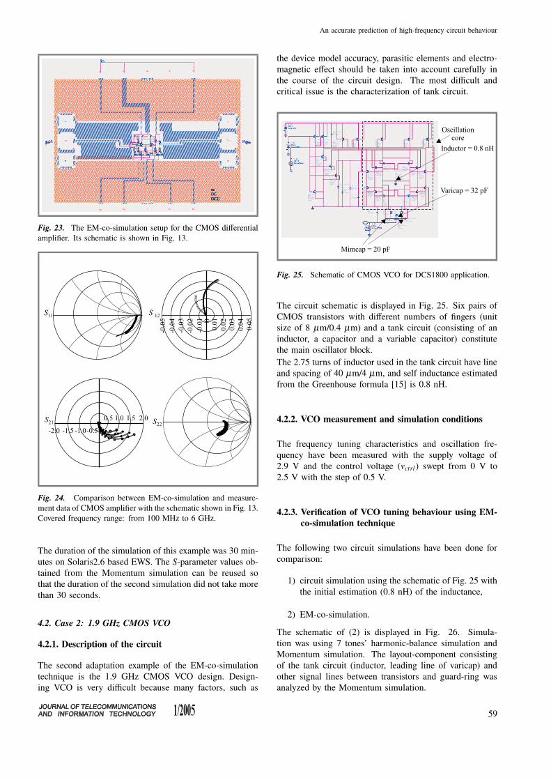
Fig. 15. Simulated frequency behaviour of LS and RS (a), Cox (b), Csub (c) and Rsub (d) of the three signal lines. Covered frequency
range: from 100 MHz to 10 GHz.
Both Rsub1(2) and Csub1(2) can be defined by the real
and imaginary part of Zsub1(2), respectively. Figure 15
displays model parameters of the three signal lines, cal-
culated by the formulae given in Table 3 (symmetrical
topology (Y1 = Y2) is applied). Table 4 lists the obtained
values.
4.1.4. Implementation of Momentum for the extrinsic
parameter extraction of MOSFET models
The estimation of RG, RB, CGD FI , and CGS FI shown in
Fig. 6 is very complex because they can hardly be recog-
nized by the measurement data of the real device. Never-
theless, their accurate values should be extracted because
they have strong influence on the high frequency character-
istics.
The RG value was extracted by the Momentum simula-
tion using MOSFET layout data (configured by 5 fin-
gers of 20 µm length with single-sided contact) of the
gate electrode material as shown in Fig. 16. The two
port y-parameters have been calculated between input port
and 5 opposite ends. The RG has been extracted by the real
part of the resultant y21:
RG = Re(
− 1y21
)
. (30)
Frequency dependency of RG is plotted in Fig. 17. Ex-
tracted RG value is approximately 13 Ω and is almost fre-
quency independent. By comparing the estimated value as
calculated in Eq. (24), it can be concluded that Eq. (13),
used to calculate the initial value, can predict the RG value
with acceptable accuracy.
The determination of both CGD FI and CGS FI has been done
in the same manner. The layout data shown in Fig. 18 was
used for Momentum simulation. Both CGD FI and CGS FIhave been calculated using the imaginary part of resultant
y21 value:
CGS FI ,CGD FI =1
2π f Im(
1y21
) . (31)
The result is shown in Fig. 19. Both capacitances are almost
independent of the frequency and amounted to about 5 fF
each.
56

An accurate prediction of high-frequency circuit behaviour
Fig. 16. Momentum setup for the extraction of RG. Simulation
target is the gate electrode material with 5 fingers of 20 µm length.
Fig. 17. Resultant RG obtained using the setup shown in Fig. 16.
Covered frequency range: from 100 MHz to 10 GHz.
The extraction of RB was done as the last step. RB has
a strong effect on the S22 value of the circuit. This is
because the output impedance of MOSFET, which forms
the source-follower network, has a strong influence on the
circuit’s S22. Mathematical optimization has been used to
extract RB. The effect of RB on the circuit’s S-parameters
is displayed in Fig. 20. At RB value of 180 Ω, best fit with
the measurement was obtained. All parameters extracted
in this section are summarized in Fig. 6.
With the lumped model of the signal lines and modi-
fied EKV2.6 model, the final simulation was performed.
Fig. 18. (a) Setup for the extraction of CGS FI and CGD FI ;
(b) resultant current flow obtained from Momentum simulation.
Simulation target is the gate material with the configuration as
shown in Fig. 6.
Fig. 19. Extracted CGD FI and CGS FI . Covered frequency range:
from 100 MHz to 10 GHz.
57

Sadayuki Yoshitomi, Hideki Kimijima, Kenji Kojima, and Hideyuki Kokatsu
Fig. 20. Effect of RB as shown in Fig. 6 on the S-parameters
of the differential amplifier. Covered frequency range: from
100 MHz to 6 GHz.
Fig. 21. Final simulation results with subcircuit-based RF-
MOSFET (as shown in Fig. 6) and lumped signal line models
(as shown in Fig. 13). Covered frequency range: from 100 MHz
to 6 GHz.
The results are shown in Fig. 21. As seen, the simulated
and measured S-parameter values are in very good agree-
ment. Thus, the simulation accuracy of an RF circuit can
be enhanced by the use of a proper device model and EM
simulation.
4.1.5. Verification of amplifier behaviour using EM-co-
simulation technique
As an extended example, EM-co-simulation technique will
be presented in this section. The flow chart to execute
EM-co-simulation is illustrated in Fig. 22. A layout-compo-
nent, that is a symbolized layout block, can be used together
with SPICE compact models as shown in Fig. 23. Agi-
lent’s ADS-2003C with Verilog-A code of EKV2.6 model
was used for this simulation.
Fig. 22. Simulation flow of electro-magnetic co-simulation.
Figure 23 illustrates the view of the simulation schematic.
The core part of the circuit is composed of spice compo-
nents (transistors, resistors and capacitors), and other ex-
ternal components such as signal lines, pads are contained
inside the layout-components.
At the first step of the simulation, EM simulation is
invoked to analyze the S-parameters of the layout-com-
ponent. After its completion, circuit simulation is followed
by the use of the resultant S-parameters and compact model.
Now that both accurate transistor model and EM simu-
lation methodology is available, simulation results shows
good agreement with the measurement data as shown
in Fig. 24.
58
An accurate prediction of high-frequency circuit behaviour
Fig. 23. The EM-co-simulation setup for the CMOS differential
amplifier. Its schematic is shown in Fig. 13.
Fig. 24. Comparison between EM-co-simulation and measure-
ment data of CMOS amplifier with the schematic shown in Fig. 13.
Covered frequency range: from 100 MHz to 6 GHz.
The duration of the simulation of this example was 30 min-
utes on Solaris2.6 based EWS. The S-parameter values ob-
tained from the Momentum simulation can be reused so
that the duration of the second simulation did not take more
than 30 seconds.
4.2. Case 2: 1.9 GHz CMOS VCO
4.2.1. Description of the circuit
The second adaptation example of the EM-co-simulation
technique is the 1.9 GHz CMOS VCO design. Design-
ing VCO is very difficult because many factors, such as
the device model accuracy, parasitic elements and electro-
magnetic effect should be taken into account carefully in
the course of the circuit design. The most difficult and
critical issue is the characterization of tank circuit.
Fig. 25. Schematic of CMOS VCO for DCS1800 application.
The circuit schematic is displayed in Fig. 25. Six pairs of
CMOS transistors with different numbers of fingers (unit
size of 8 µm/0.4 µm) and a tank circuit (consisting of an
inductor, a capacitor and a variable capacitor) constitute
the main oscillator block.
The 2.75 turns of inductor used in the tank circuit have line
and spacing of 40 µm/4 µm, and self inductance estimated
from the Greenhouse formula [15] is 0.8 nH.
4.2.2. VCO measurement and simulation conditions
The frequency tuning characteristics and oscillation fre-
quency have been measured with the supply voltage of
2.9 V and the control voltage (vctrl) swept from 0 V to
2.5 V with the step of 0.5 V.
4.2.3. Verification of VCO tuning behaviour using EM-
co-simulation technique
The following two circuit simulations have been done for
comparison:
1) circuit simulation using the schematic of Fig. 25 with
the initial estimation (0.8 nH) of the inductance,
2) EM-co-simulation.
The schematic of (2) is displayed in Fig. 26. Simula-
tion was using 7 tones’ harmonic-balance simulation and
Momentum simulation. The layout-component consisting
of the tank circuit (inductor, leading line of varicap) and
other signal lines between transistors and guard-ring was
analyzed by the Momentum simulation.
59

Sadayuki Yoshitomi, Hideki Kimijima, Kenji Kojima, and Hideyuki Kokatsu
Fig. 26. Simulation setup of EM-co-simulation for CMOS VCO
tuning characteristics.
Fig. 27. Comparison of simulation results between EM-co-simu-
lation and measurement of tuning characteristics of CMOS VCO.
Fig. 28. Comparison of simulation characteristics of the inductor in the tank circuit between lumped model and Momentum. Model
parameter values are displayed in the figure.
60
An accurate prediction of high-frequency circuit behaviour
Simulation results for the two cases are compared in
Fig. 27. The frequency deviation in the case (1) ranged
between 330 MHz and 400 MHz from vctrl = 0 V to
vctrl = 2.0 V, which approximately amounted to the fre-
quency error of 16%–18%. In the case (2), the deviation
has been drastically decreased to only 3 MHz difference
from the measurement in the whole vctrl range. Thus, it
can be concluded that EM-co-simulation is accurate and
effective for the design of VCO circuits.
4.2.4. Detailed analysis of the tank circuit
The reason for the obtained accuracy in the case (2) seems
to be the increase of the inductance in the tank circuit. This
is confirmed by the Momentum analysis of the tank circuit
layout. The values of the equivalent circuit as shown in
Fig. 14 are Ls = 1.12 nH, Rs = 2.06 Ω, Cox1(2) = 490 fF,
Csub1(2) = 50 fF and Rsub1(2) = 414 Ω. Figure 28 shows the
comparison of simulation data of equivalent circuit with
Momentum output.
The resultant Ls was 1.12 nH (a visible increase from
the initial estimation of 0.8 nH), which means that the
oscillation frequency was decreased by 15%. This in-
creased inductance is ascribed to the parasitic induc-
tances of the inductor’s extension part, mutual coupling
with the surrounding guard ring, and other electrical
coupling.
Based on the above results, it can be concluded that the
EM-co-simulation can incorporate the parasitic effects that
cannot easily be estimated from the layout, and provides
the circuit designer with the accurate prediction of high
frequency circuit behaviour.
5. Conclusions
In this study, it has been proved that the proper use of
good CMOS SPICE model (EKV2.6) and electro-magnetic
simulation can yield a good match between measured and
simulated data. Through the investigation of the applica-
bility of EM simulation, using several test structures, it has
been concluded that EM simulation is very useful for the
estimation of inductor characteristics, layout parasitic com-
ponents in the circuit and the extrinsic part of the transistor.
EM-co-simulation is introduced as a new simulation tech-
nique. This can be used as a “post-layout tool” because of
its acceptable accuracy.
To summarize, it can be concluded again that the use of
both: accurate transistor model and electro-magnetic sim-
ulation is the shortest route to predict the behaviour of RF
circuits in the most accurate way.
Acknowledgements
The Authors would like to express their gratitude to
Dr. Matthias Bucher the Department of Electronics and
Computer Engineering at Technical University of Crete for
technical comments on the extraction of EKV2.6 model
parameters and to Dr. Władysław Grabiński at Freescale
Semiconductor Geneva Modeling and Characterization Lab
for heartfelt support.
References
[1] “ADS 2003C reference manual”, Agilent Technologies, 2003.
[2] “HSPICE2002.2 model manual”, Synopsis, 2002.
[3] C. Enz, F. Krummenacher, and E. Vittoz, “An analytical MOS
transistor model valid in all regions of operation and dedicated to
low-voltage and low-current applications”, J. Anal. Integr. Circ. Sig.
Proc., no. 8, pp. 83–114, 1995.
[4] M. Bucher, C. Lallement, C. Enz, F. Théodoloz, and F. Krummen-
acher, “The EPFL-EKV MOSFET model equations for simulation,
Version 2.6”, Tech. Rep., Electronics Laboratory, Swiss Federal In-
stitute of Technology Lausanne (EPFL), June 1997.
[5] M. Bucher, “Analytical MOS transistor modelling for analog circuit
simulation”, Ph.D. thesis, no. 2114, Lausanne, EPFL, 1999.
[6] STARC Physical Design Gr, “HiSIM1.2.0 release note”, Apr. 2003,
http://home.hiroshima-u.ac.jp/usdl/HiSIM.shtml
[7] G. Gildenblat and T. L. Chen, “Overview of an advanced surface-
potential-based MOSFET model”, in Tech. Proc. Fifth Int. Conf.
Model. Simul. Microsyst., Puerto Rico, 2002, pp. 657–661.
[8] “BSIM3V3 MOSFET model”,
http://www.device.eecs.berkeley.edu/ bsim3
[9] “BSIM4 MOSFET model”,
http://www.device.eecs.berkeley.edu/ bsim4
[10] Minitab Inc. “MINITABrfor Windows release 12.21 manual”,
1998.
[11] C. Enz, “An MOS transistor model for RF IC design valid in all
regions of operation”, IEEE Trans. Microw. Theory Tech., vol. 50,
no. 1, 2002.
[12] M. J. Deen and T. A. Fieldy, “CMOS RF modeling characterization
and applications”, World Sci., 2002.
[13] F. Krummenacher, M. Bucher, and W. Grabiński, “Deliverable D2.1,
RF EKV MOSFET model implementation”, CRAFT, Eur. Project,
no. 25710, WP2, July 2000.
[14] F. Krummenacher, M. Bucher, and W. Grabiński, “Deliverable D2.2,
RF EKV MOSFET model implementation”, CRAFT, Eur. Project,
no. 25710, WP2, July 2000.
[15] H. M. Greenhouse, “Design of planar rectangular microelectronic
inductors”, IEEE Trans. Parts, Hybr., Packag., vol. PHP-10, no. 2,
June 1974.
[16] S. S. Mohan, “Modeling, design and optimization of on-chip induc-
tors and transformers”, CIS, Stanford University, June 1999.
Sadayuki Yoshitomi was born
in Sasebo, Japan, in 1965. He
received the B.E. and M.E, and
Ph.D. degrees from Yokohama
National University, Yokohama,
Japan, 1988, 1990, and 1993,
respectively. The title of his
doctor thesis was the “The stu-
dy on the silicon dioxide film
deposited by liquid phase depo-
sition (LPD)”. His background
61
Sadayuki Yoshitomi, Hideki Kimijima, Kenji Kojima, and Hideyuki Kokatsu
is the physics of Si/SiO2 interface. In 1993, he joined
the Research and Development Center, Toshiba Corpora-
tion, Kawasaki, Japan, where he was engaged in the re-
search and development of BiCMOS device technologies.
His current field of interest is the application of simulation
technologies for telecommunication applications such as
system simulation for next generation ICs, electro-magnetic
simulation and SPICE modelling.
e-mail: [email protected]
TOSHIBA Corporation Semiconductor Company
Microelectronics Center
2-5-1 Kasama, Sakae-Ku
Yokohama-City, Kanagawa, 247-8585 Japan
Hideki Kimijima was born in
Yokohama, Japan, in 1973. He
received the B.E. and M.E. de-
grees from Yokohama National
University, Yokohama, Japan,
in 1995 and 1997, respectively.
In 1997, he joined Microelec-
tronics Engineering Laboratory,
Toshiba Corporation, Kawasaki,
Japan, where he was engaged
in the research and development
of device technology of RF-CMOS. Since 2000, he has
been involved for the research and development of de-
vice technology of RF BiCMOS, especially SiGe BiCMOS
process in Semiconductor Company, Toshiba Corporation,
Kawasaki, Japan. His current interests are device physics
of bipolar transistor and CMOS.
e-mail: [email protected]
TOSHIBA Corporation Semiconductor Company
Microelectronics Center at Kitakyushu Operation
1-10-1 Shimoitozu, Kokura-Kita-Ku
Kitakyuushyu-City, Fukuoka, 803-8686 Japan
Kenji Kojima received the B.E.
and M.E. degrees in electri-
cal engineering from Kanagawa
University, Yokohama, Japan,
in 1990 and 1992, respectively.
In 1992, he joined the Medical
Equipment Division of Toshiba
Corporation, Tochigi, Japan.
In 1996, he joined the Semi-
conductor Division, Toshiba
Corporation, Kanagawa, Japan.
Since 2001, he has been engaged in the research and devel-
opment of device technology of advanced CMOS analogue
and logic in SoC research and development center.
e-mail: [email protected]
TOSHIBA Corporation Semiconductor Company
Advanced CMOS Technology Department
Soc Research and Development Center
8 Shinsugita-Cho, Isogo-ku
Yokohama-City, Kanagawa, 235-8522 Japan
Hideyuki Kokatsu was born
in Tokyo, Japan, in 1967. He
received the B.S. and M.S.
degrees in theoretical physics
from Shizuoka University, Shi-
zuoka, Japan, in 1990 and 1992,
respectively. In 1992, he joined
the Semiconductor System En-
gineering Center, Toshiba Cor-
poration, Kawasaki, Japan. He
currently is engaged in the de-
sign and development of high-frequency analogue inte-
grated.
e-mail: [email protected]
TOSHIBA Corporation Semiconductor Company
Microelectronics Center
2-5-1 Kasama, Sakae-Ku
Yokohama-City, Kanagawa, 247-8585 Japan
62