AN 835: PAM4 Signaling Fundamentals · 2019-09-23 · In many electrical interface standards such...
52
AN 835: PAM4 Signaling Fundamentals Subscribe Send Feedback AN-835 | 2019.03.12 Latest document on the web: PDF | HTML
Transcript of AN 835: PAM4 Signaling Fundamentals · 2019-09-23 · In many electrical interface standards such...
AN 835: PAM4 SignalingFundamentals
SubscribeSend Feedback
AN-835 | 2019.03.12Latest document on the web: PDF | HTML
Contents
1. Introduction................................................................................................................... 41.1. NRZ Fundamentals................................................................................................ 41.2. Standards Using PAM4 Coding Scheme..................................................................... 71.3. CEI-56G Interconnect Reaches and Application Distances............................................8
1.3.1. VSR (Very Short Reach) Chip-to-Module....................................................... 91.3.2. MR (Mid-Range Reach) - Chip to Chip Within a PCBA...................................... 91.3.3. LR (Long Reach) - Chip to Chip Across a Backplane/Midplane or a Cable............9
2. CEI-56G-MR Transmitter...............................................................................................112.1. Naming Conventions............................................................................................ 112.2. Eye Height (EH6) and Eye Width (EW6).................................................................. 112.3. Eye Linearity....................................................................................................... 132.4. Electrical Characteristics....................................................................................... 14
2.4.1. Transmitter Characteristics........................................................................142.4.2. Transmitter Return Loss............................................................................ 152.4.3. Transmitter Linearity (RLM)........................................................................ 172.4.4. Signal-to-Noise-and-Distortion Ratio (SNDR)............................................... 18
2.5. PAM4 Jitter Methodology.......................................................................................192.6. TX Pre-Emphasis Method...................................................................................... 19
3. CEI-56G-MR-PAM4 Interface Details.............................................................................223.1. COM Introduction.................................................................................................22
3.1.1. Backplane Measurements..........................................................................233.2. Normative Channel Specification COM.....................................................................283.3. Informative Channel Insertion Loss........................................................................ 303.4. Informative Channel Return Loss........................................................................... 31
4. CEI-56G-MR-PAM4 Receiver..........................................................................................324.1. Challenges in Analyzing PAM4 Signals.....................................................................324.2. PAM4 Receiver Architecture...................................................................................33
4.2.1. Analog vs. Digital Receiver........................................................................ 334.2.2. Slicer..................................................................................................... 334.2.3. Clock and Data Recovery (CDR)................................................................. 33
4.3. Equalization Technique......................................................................................... 334.4. CEI-56G-MR-PAM4 Receiver Details........................................................................ 34
4.4.1. Electrical Characteristics........................................................................... 344.4.2. Receiver Input Return Loss........................................................................354.4.3. Receiver Interference Tolerance................................................................. 364.4.4. Receiver Jitter Tolerance........................................................................... 36
5. PAM4 Link Case Study...................................................................................................385.1. OIF_Stressed...................................................................................................... 38
5.1.1. Channel Characteristics.............................................................................395.1.2. OIF_Stressed PAM4 Link Simulation with the Advanced Link Analyzer..............41
5.2. OIF_Compliant.................................................................................................... 425.2.1. Channel Characteristics.............................................................................435.2.2. OIF_Compliant PAM4 Link Simulation with the Advanced Link Analyzer............45
Contents
AN 835: PAM4 Signaling Fundamentals Send Feedback
2
6. Medium Reach (MR) PAM4 System Design Study.......................................................... 476.1. System Power..................................................................................................... 476.2. System Cost........................................................................................................476.3. Board Space........................................................................................................476.4. Conclusion.......................................................................................................... 48
7. Glossary and Acronyms.................................................................................................49
8. References....................................................................................................................51
9. Document Revision History for AN 835: PAM4 Signaling Fundamentals........................ 52
Contents
Send Feedback AN 835: PAM4 Signaling Fundamentals
3
1. IntroductionThis Pulse-Amplitude Modulation 4-Level (PAM4) application note explains PAM4theory and operation while introducing the Intel® Stratix® 10 TX device capability andthe realization of 57.8 Gbps data rate applications.
The application note uses 56 Gbps to describe data rates in general because of thebaseline established in the Common Electrical Interface (CEI). However, the actualdata rate can be up to 57.8 Gbps.
1.1. NRZ Fundamentals
Ethernet is a family of computer networking technologies that is most widely used inlocal area networks (LAN), metropolitan area networks (MAN) and wide area networks(WAN).
Since its commercial introduction in 1980 and first standardization in 1983, Ethernetcontinues to support increasing demands for a connected world with instant datatransmission. Development of 100G Ethernet is currently underway. Achieving greaterEthernet speeds like 200G/400G requires a significant technological advancement.Two coding schemes are possible: Non-Return-to-Zero (NRZ), also known as Pulse-Amplitude Modulation 2-Level (PAM2), and Pulse-Amplitude Modulation 4-Level(PAM4). Because of NRZ’s higher Nyquist frequency which results in higher channel-dependent loss, PAM4 has become a more viable solution.
NRZ is a modulation technique that has two voltage levels to represent logic 0 andlogic 1. PAM4 uses four voltage levels to represent four combinations of two bits logic– 11, 10, 01, and 00. Refer to Standards Using PAM4 Coding Scheme for more detailsabout PAM4 naming conventions. Each of the modulation schemes comes with aunique set of advantages and disadvantages.
AN-835 | 2019.03.12
Send Feedback
Intel Corporation. All rights reserved. Intel, the Intel logo, Altera, Arria, Cyclone, Enpirion, MAX, Nios, Quartusand Stratix words and logos are trademarks of Intel Corporation or its subsidiaries in the U.S. and/or othercountries. Intel warrants performance of its FPGA and semiconductor products to current specifications inaccordance with Intel's standard warranty, but reserves the right to make changes to any products and servicesat any time without notice. Intel assumes no responsibility or liability arising out of the application or use of anyinformation, product, or service described herein except as expressly agreed to in writing by Intel. Intelcustomers are advised to obtain the latest version of device specifications before relying on any publishedinformation and before placing orders for products or services.*Other names and brands may be claimed as the property of others.
ISO9001:2015Registered
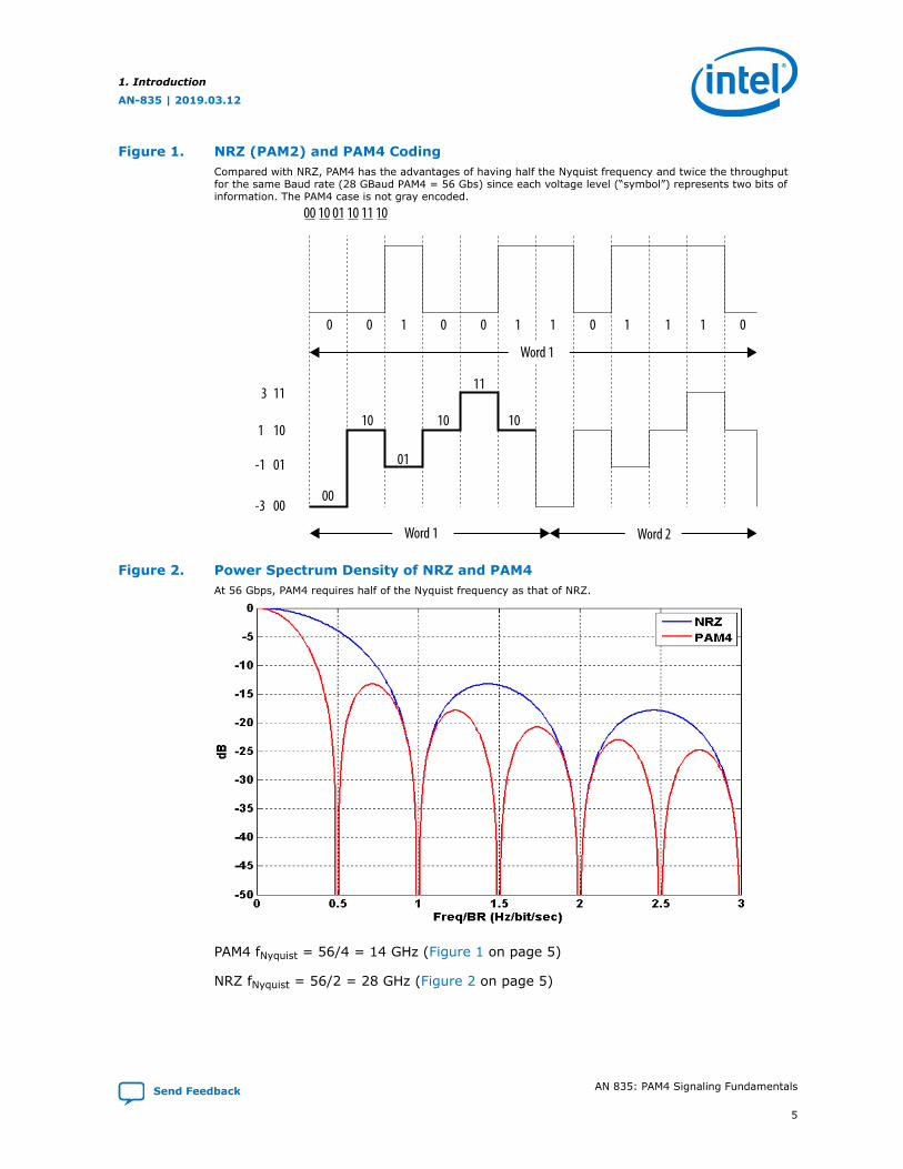
Figure 1. NRZ (PAM2) and PAM4 CodingCompared with NRZ, PAM4 has the advantages of having half the Nyquist frequency and twice the throughputfor the same Baud rate (28 GBaud PAM4 = 56 Gbs) since each voltage level (“symbol”) represents two bits ofinformation. The PAM4 case is not gray encoded.
00
10
01
10
11
10
0 0 1 0 0 1 1 0 1 1 1 0
3
1
-1
-3
00 10 01 10 11 10
00
01
10
11
Word 1 Word 2
Word 1
Figure 2. Power Spectrum Density of NRZ and PAM4At 56 Gbps, PAM4 requires half of the Nyquist frequency as that of NRZ.
PAM4 fNyquist = 56/4 = 14 GHz (Figure 1 on page 5)
NRZ fNyquist = 56/2 = 28 GHz (Figure 2 on page 5)
1. Introduction
AN-835 | 2019.03.12
Send Feedback AN 835: PAM4 Signaling Fundamentals
5
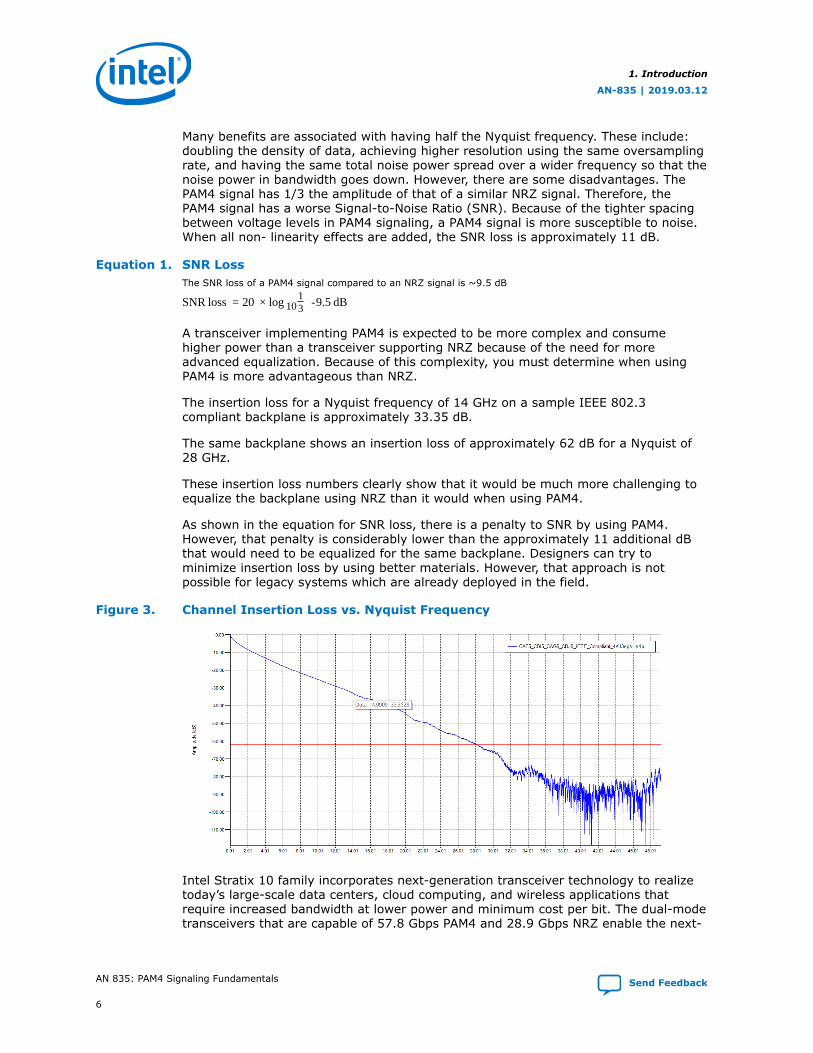
Many benefits are associated with having half the Nyquist frequency. These include:doubling the density of data, achieving higher resolution using the same oversamplingrate, and having the same total noise power spread over a wider frequency so that thenoise power in bandwidth goes down. However, there are some disadvantages. ThePAM4 signal has 1/3 the amplitude of that of a similar NRZ signal. Therefore, thePAM4 signal has a worse Signal-to-Noise Ratio (SNR). Because of the tighter spacingbetween voltage levels in PAM4 signaling, a PAM4 signal is more susceptible to noise.When all non- linearity effects are added, the SNR loss is approximately 11 dB.
Equation 1. SNR LossThe SNR loss of a PAM4 signal compared to an NRZ signal is ~9.5 dB
SNR loss = 20 × log 1013 ≃ -9.5 dB
A transceiver implementing PAM4 is expected to be more complex and consumehigher power than a transceiver supporting NRZ because of the need for moreadvanced equalization. Because of this complexity, you must determine when usingPAM4 is more advantageous than NRZ.
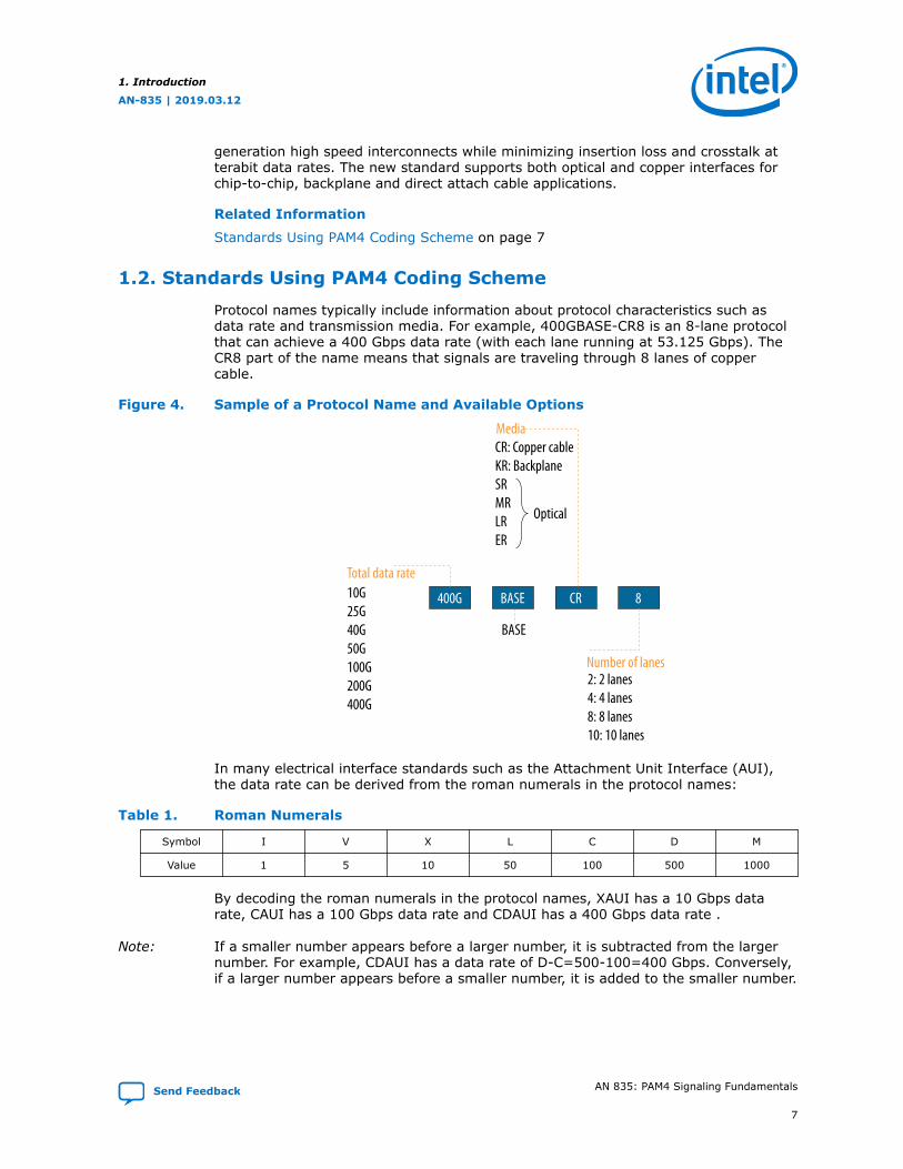
The insertion loss for a Nyquist frequency of 14 GHz on a sample IEEE 802.3compliant backplane is approximately 33.35 dB.
The same backplane shows an insertion loss of approximately 62 dB for a Nyquist of28 GHz.
These insertion loss numbers clearly show that it would be much more challenging toequalize the backplane using NRZ than it would when using PAM4.
As shown in the equation for SNR loss, there is a penalty to SNR by using PAM4.However, that penalty is considerably lower than the approximately 11 additional dBthat would need to be equalized for the same backplane. Designers can try tominimize insertion loss by using better materials. However, that approach is notpossible for legacy systems which are already deployed in the field.
Figure 3. Channel Insertion Loss vs. Nyquist Frequency
Intel Stratix 10 family incorporates next-generation transceiver technology to realizetoday’s large-scale data centers, cloud computing, and wireless applications thatrequire increased bandwidth at lower power and minimum cost per bit. The dual-modetransceivers that are capable of 57.8 Gbps PAM4 and 28.9 Gbps NRZ enable the next-
1. Introduction
AN-835 | 2019.03.12
AN 835: PAM4 Signaling Fundamentals Send Feedback
6
generation high speed interconnects while minimizing insertion loss and crosstalk atterabit data rates. The new standard supports both optical and copper interfaces forchip-to-chip, backplane and direct attach cable applications.
Related Information
Standards Using PAM4 Coding Scheme on page 7
1.2. Standards Using PAM4 Coding Scheme
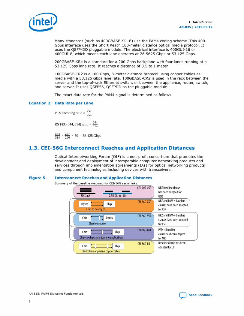
Protocol names typically include information about protocol characteristics such asdata rate and transmission media. For example, 400GBASE-CR8 is an 8-lane protocolthat can achieve a 400 Gbps data rate (with each lane running at 53.125 Gbps). TheCR8 part of the name means that signals are traveling through 8 lanes of coppercable.
Figure 4. Sample of a Protocol Name and Available Options
400G BASE CR
Total data rate10G25G40G50G100G200G400G
BASE
Media
Optical
CR: Copper cableKR: BackplaneSRMRLRER
8
Number of lanes2: 2 lanes4: 4 lanes8: 8 lanes10: 10 lanes
In many electrical interface standards such as the Attachment Unit Interface (AUI),the data rate can be derived from the roman numerals in the protocol names:
Table 1. Roman Numerals
Symbol I V X L C D M
Value 1 5 10 50 100 500 1000
By decoding the roman numerals in the protocol names, XAUI has a 10 Gbps datarate, CAUI has a 100 Gbps data rate and CDAUI has a 400 Gbps data rate .
Note: If a smaller number appears before a larger number, it is subtracted from the largernumber. For example, CDAUI has a data rate of D-C=500-100=400 Gbps. Conversely,if a larger number appears before a smaller number, it is added to the smaller number.
1. Introduction
AN-835 | 2019.03.12
Send Feedback AN 835: PAM4 Signaling Fundamentals
7
Many standards (such as 400GBASE-SR16) use the PAM4 coding scheme. This 400-Gbps interface uses the Short Reach 100-meter distance optical media protocol. Ituses the QSFP-DD pluggable module. The electrical interface is 400GUI-16 or400GUI-8, which means each lane operates at 26.5625 Gbps or 53.125 Gbps.
200GBASE-KR4 is a standard for a 200 Gbps backplane with four lanes running at a53.125 Gbps lane rate. It reaches a distance of 0.5 to 1 meter.
100GBASE-CR2 is a 100 Gbps, 3-meter distance protocol using copper cables asmedia with a 53.125 Gbps lane rate. 100GBASE-CR2 is used in the rack between theserver and the top-of-rack Ethernet switch, or between the appliance, router, switch,and server. It uses QSFP56, QSFPDD as the pluggable module.
The exact data rate for the PAM4 signal is determined as follows:
Equation 2. Data Rate per Lane
PCS encoding ratio =257256
RS FEC(544, 514) ratio =544514
544514 ×
257256 × 50 = 53.125 Gbps
1.3. CEI-56G Interconnect Reaches and Application Distances
Optical Internetworking Forum (OIF) is a non-profit consortium that promotes thedevelopment and deployment of interoperable computer networking products andservices through implementation agreements (IAs) for optical networking productsand component technologies including devices with transceivers.
Figure 5. Interconnect Reaches and Application DistancesSummary of the baseline roadmap for CEI-56G serial links.
3D Stack 2.5D Die-to-die
CEI-56G-USR
Optics ChipChip to nearby OE
CEI-56G-XSR
Chip Optics
Chip Chip
Chip to module
CEI-56G-VSR
Chip-to-chip and midplane applications
CEI-56G-MR
Chip ChipBackplane or passive copper cable
CEI-56G-LR
NRZ baseline clausehas been adopted for USRNRZ and PAM-4 baselineclauses have been adoptedfor XSR
NRZ and PAM-4 baselineclauses have been adoptedfor VSR
PAM-4 baselineclause has been adoptedfor MRBaseline clause has beenadopted for LR
1. Introduction
AN-835 | 2019.03.12
AN 835: PAM4 Signaling Fundamentals Send Feedback
8
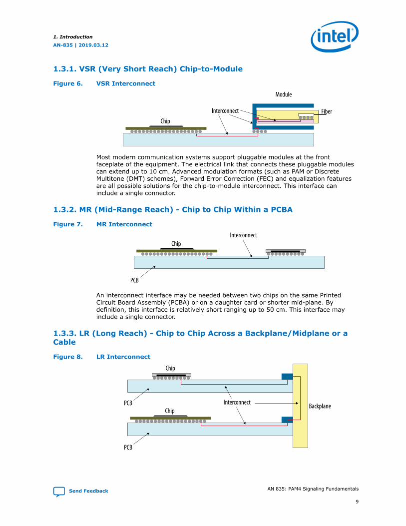
1.3.1. VSR (Very Short Reach) Chip-to-Module
Figure 6. VSR Interconnect
Module
Interconnect FiberChip
Most modern communication systems support pluggable modules at the frontfaceplate of the equipment. The electrical link that connects these pluggable modulescan extend up to 10 cm. Advanced modulation formats (such as PAM or DiscreteMultitone (DMT) schemes), Forward Error Correction (FEC) and equalization featuresare all possible solutions for the chip-to-module interconnect. This interface caninclude a single connector.
1.3.2. MR (Mid-Range Reach) - Chip to Chip Within a PCBA
Figure 7. MR Interconnect
ChipInterconnect
PCB
An interconnect interface may be needed between two chips on the same PrintedCircuit Board Assembly (PCBA) or on a daughter card or shorter mid-plane. Bydefinition, this interface is relatively short ranging up to 50 cm. This interface mayinclude a single connector.
1.3.3. LR (Long Reach) - Chip to Chip Across a Backplane/Midplane or aCable
Figure 8. LR Interconnect
ChipInterconnect
PCB
Chip
BackplanePCB
1. Introduction
AN-835 | 2019.03.12
Send Feedback AN 835: PAM4 Signaling Fundamentals
9
This interface communicates between two cards across a backplane or midplane withina chassis and is less than 1 meter with up to two connectors. KP-FEC may be arequirement to meet the BER.
Table 2. Summary of CEI 56G Different Reaches and Distances
Parameter Ultra Short Reach(USR)
Extra ShortReach (XSR) VSR MR LR
Reach 2.5D/3D Chip- to-opticsEngine Chip- to-module Chip-to-chip Chip-to-chip over
a backplane
Data Rate (Gbps) 19.6-58 39.2-58 39.2-58 36-58 36-58
BER (pre-FEC) 1E-15 1E-15 1E-6 1E-6 1E-4
Distance 10 mm (~0.4") 50 mm (~2") 150 mm (~6") 500 mm (~20") 1000 mm (~40")
Interconnect MCM PCB+0 connector PCB+1 connector PCB+1 connector PCB+2 connectors
Insertion Loss(dB) 2@28 GHz (NRZ) 4@14 GHz (PAM4) 10@14 GHz
(PAM4)20@14 GHz
(PAM4)30@14 GHz
(PAM4)
Modulation NRZ PAM4 or NRZ PAM4 or NRZ PAM4 or NRZ PAM4 or ENRZ
FEC No No Yes/No Yes/No Yes/No
Table 3. Summary of Ethernet 50G/Lane Standards
Reach 400GBE (802.3bs) 200GBE(802.3bs, .cd) 100GBE (802.3cd) 50GBE (802.3cd)
Chip-to-chip (C2C)and Chip-to-module
(C2M)400GAUI-8 200GAUI-4 — —
Backplane (BP) — 200GBASE-KR4 100GBASE-KR2 50GBASE-KR
Copper Cable (CC) — 200GBASE-CR4 100GBASE-CR2 50GBASE-CR
1. Introduction
AN-835 | 2019.03.12
AN 835: PAM4 Signaling Fundamentals Send Feedback
10
2. CEI-56G-MR TransmitterThis section discusses the CEI-56G-MR transmitter electrical specifications, jittermethodologies and terms and the pre-emphasis method.
2.1. Naming Conventions
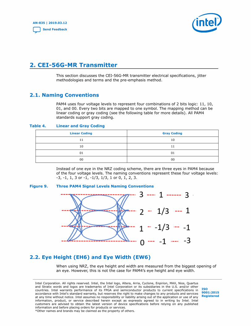
PAM4 uses four voltage levels to represent four combinations of 2 bits logic: 11, 10,01, and 00. Every two bits are mapped to one symbol. The mapping method can belinear coding or gray coding (see the following table for more details). All PAM4standards support gray coding.
Table 4. Linear and Gray Coding
Linear Coding Gray Coding
11 10
10 11
01 01
00 00
Instead of one eye in the NRZ coding scheme, there are three eyes in PAM4 becauseof the four voltage levels. The naming conventions represent these four voltage levels:-3, -1, 1, 3 or -1, -1/3, 1/3, 1 or 0, 1, 2, 3.
Figure 9. Three PAM4 Signal Levels Naming Conventions
2.2. Eye Height (EH6) and Eye Width (EW6)
When using NRZ, the eye height and width are measured from the biggest opening ofan eye. However, this is not the case for PAM4’s eye height and eye width.
AN-835 | 2019.03.12
Send Feedback
Intel Corporation. All rights reserved. Intel, the Intel logo, Altera, Arria, Cyclone, Enpirion, MAX, Nios, Quartusand Stratix words and logos are trademarks of Intel Corporation or its subsidiaries in the U.S. and/or othercountries. Intel warrants performance of its FPGA and semiconductor products to current specifications inaccordance with Intel's standard warranty, but reserves the right to make changes to any products and servicesat any time without notice. Intel assumes no responsibility or liability arising out of the application or use of anyinformation, product, or service described herein except as expressly agreed to in writing by Intel. Intelcustomers are advised to obtain the latest version of device specifications before relying on any publishedinformation and before placing orders for products or services.*Other names and brands may be claimed as the property of others.
ISO9001:2015Registered
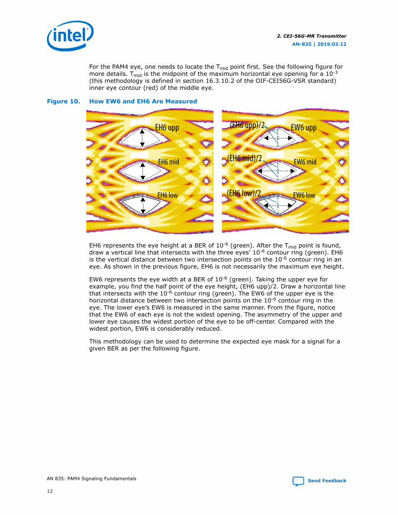
For the PAM4 eye, one needs to locate the Tmid point first. See the following figure formore details. Tmid is the midpoint of the maximum horizontal eye opening for a 10-3
(this methodology is defined in section 16.3.10.2 of the OIF-CEI56G-VSR standard)inner eye contour (red) of the middle eye.
Figure 10. How EW6 and EH6 Are Measured
EH6 upp
EH6 mid
EH6 low
EW6 upp
EW6 mid
EW6 low
(EH6 upp)/2
(EH6 mid)/2
(EH6 low)/2
EH6 represents the eye height at a BER of 10-6 (green). After the Tmid point is found,draw a vertical line that intersects with the three eyes' 10-6 contour ring (green). EH6is the vertical distance between two intersection points on the 10-6 contour ring in aneye. As shown in the previous figure, EH6 is not necessarily the maximum eye height.
EW6 represents the eye width at a BER of 10-6 (green). Taking the upper eye forexample, you find the half point of the eye height, (EH6 upp)/2. Draw a horizontal linethat intersects with the 10-6 contour ring (green). The EW6 of the upper eye is thehorizontal distance between two intersection points on the 10-6 contour ring in theeye. The lower eye’s EW6 is measured in the same manner. From the figure, noticethat the EW6 of each eye is not the widest opening. The asymmetry of the upper andlower eye causes the widest portion of the eye to be off-center. Compared with thewidest portion, EW6 is considerably reduced.
This methodology can be used to determine the expected eye mask for a signal for agiven BER as per the following figure.
2. CEI-56G-MR Transmitter
AN-835 | 2019.03.12
AN 835: PAM4 Signaling Fundamentals Send Feedback
12
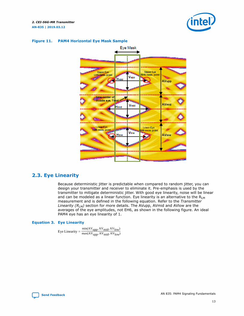
Figure 11. PAM4 Horizontal Eye Mask Sample
2.3. Eye Linearity
Because deterministic jitter is predictable when compared to random jitter, you candesign your transmitter and receiver to eliminate it. Pre-emphasis is used by thetransmitter to mitigate deterministic jitter. With good eye linearity, noise will be linearand can be modeled as a linear function. Eye linearity is an alternative to the RLMmeasurement and is defined in the following equation. Refer to the TransmitterLinearity (RLM) section for more details. The AVupp, AVmid and AVlow are theaverages of the eye amplitudes, not EH6, as shown in the following figure. An idealPAM4 eye has an eye linearity of 1.
Equation 3. Eye Linearity
Eye Linearity =min(AVupp, AVmid, AVlow)
max(AVupp, AVmid, AVlow)
2. CEI-56G-MR Transmitter
AN-835 | 2019.03.12
Send Feedback AN 835: PAM4 Signaling Fundamentals
13
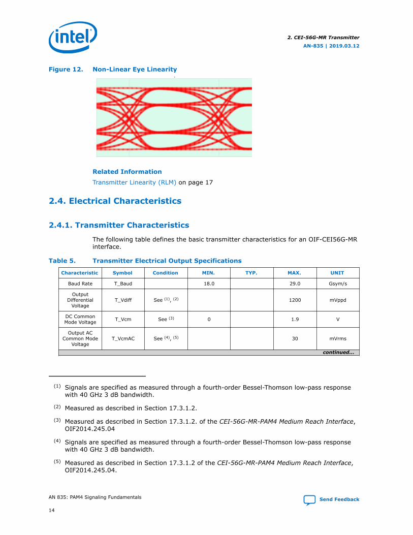
Figure 12. Non-Linear Eye Linearity
Related Information
Transmitter Linearity (RLM) on page 17
2.4. Electrical Characteristics
2.4.1. Transmitter Characteristics
The following table defines the basic transmitter characteristics for an OIF-CEI56G-MRinterface.
Table 5. Transmitter Electrical Output Specifications
Characteristic Symbol Condition MIN. TYP. MAX. UNIT
Baud Rate T_Baud 18.0 29.0 Gsym/s
OutputDifferential
VoltageT_Vdiff See (1), (2) 1200 mVppd
DC CommonMode Voltage T_Vcm See (3) 0 1.9 V
Output ACCommon Mode
VoltageT_VcmAC See (4), (5) 30 mVrms
continued...
(1) Signals are specified as measured through a fourth-order Bessel-Thomson low-pass responsewith 40 GHz 3 dB bandwidth.
(2) Measured as described in Section 17.3.1.2.
(3) Measured as described in Section 17.3.1.2. of the CEI-56G-MR-PAM4 Medium Reach Interface,OIF2014.245.04
(4) Signals are specified as measured through a fourth-order Bessel-Thomson low-pass responsewith 40 GHz 3 dB bandwidth.
(5) Measured as described in Section 17.3.1.2 of the CEI-56G-MR-PAM4 Medium Reach Interface,OIF2014.245.04.
2. CEI-56G-MR Transmitter
AN-835 | 2019.03.12
AN 835: PAM4 Signaling Fundamentals Send Feedback
14
Characteristic Symbol Condition MIN. TYP. MAX. UNIT
Single-EndedTransmitter
Output VoltageT_Vse See (6), (7) -0.3 1.9 V
DifferentialOutput Return
LossT_SDD22 (8) dB
Common ModeOutput Return
LossT_SCC22 (9) dB
LevelSeparation
Mismatch RatioT_RLM
See(10) (11)(12)
0.95 %
Steady-StateVoltage T_Vf 0.4 0.6 V
Linear Fit PulsePeak T_Pk 0.80 x T_Vf V
Signal-to-Noise-and-Distortion-
Ratio
T_SNDR 31 dB
2.4.2. Transmitter Return Loss
The following figure details the minimum permitted MR transmitter differential returnloss (RL) for 29 Gbaud/s. Notice that RLmin is -6 dB at 14.5 GHz. Using the equationfor differential return loss limit below, with f = 14.5, fb = 29, the result is RLmin =6.09 dB. This is roughly the same as the RL for an NRZ system, which means that thetransmitter operates roughly the same with existing legacy backplanes.
(6) Signals are specified as measured through a fourth-order Bessel-Thomson low-pass responsewith 40 GHz 3 dB bandwidth.
(7) Measured as described in Section 17.3.1.2 of the CEI-56G-MR-PAM4 Medium Reach Interface,OIF2014.245.04.
(8) See Equation 17-4 of the CEI-56G-MR-PAM4 Medium Reach Interface, OIF2014.245.04
(9) See Equation 17-5 of the CEI-56G-MR-PAM4 Medium Reach Interface, OIF2014.245.04
(10) Signals are specified as measured through a fourth-order Bessel-Thomson low-pass responsewith 40 GHz 3 dB bandwidth.
(11) Measured as described in Section 17.3.1.2 of the CEI-56G-MR-PAM4 Medium Reach Interface,OIF2014.245.04.
(12) Measured as described in Section 17.3.1.6 of the CEI-56G-MR-PAM4 Medium Reach Interface,OIF2014.245.04.
2. CEI-56G-MR Transmitter
AN-835 | 2019.03.12
Send Feedback AN 835: PAM4 Signaling Fundamentals
15
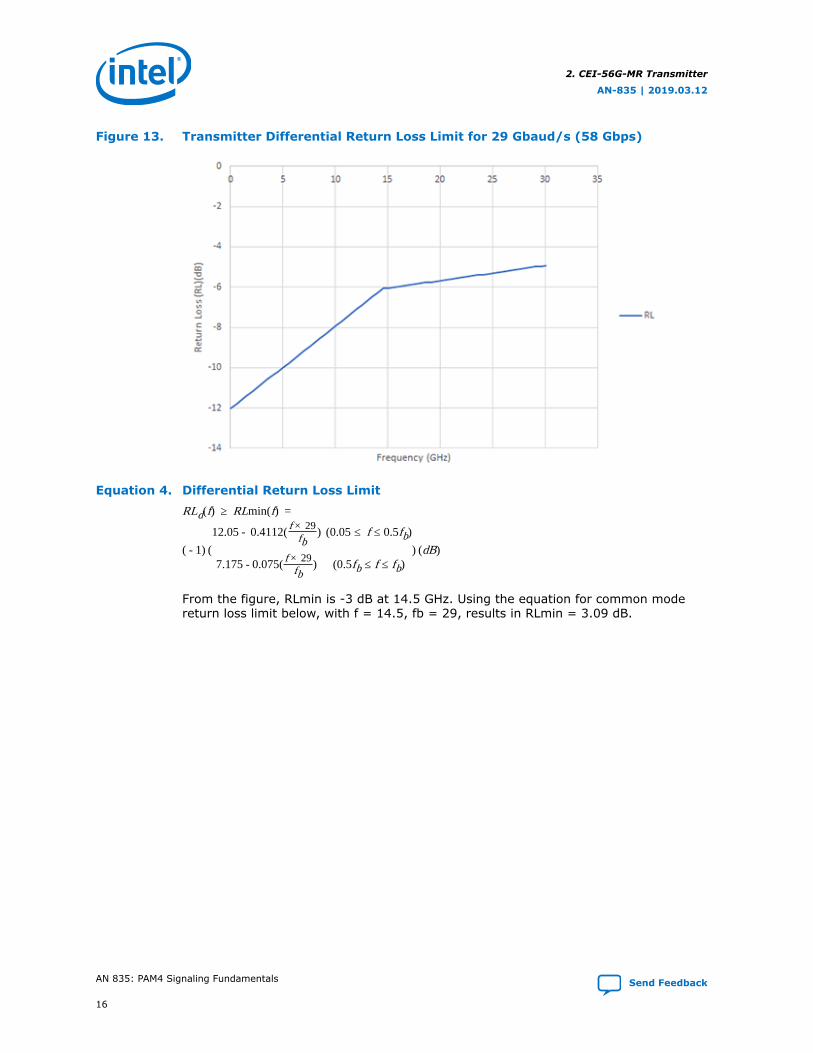
Figure 13. Transmitter Differential Return Loss Limit for 29 Gbaud/s (58 Gbps)
Equation 4. Differential Return Loss LimitRLd(f) ≥ RLmin(f) =
( - 1) (
12.05 - 0.4112(f × 29
fb) (0.05 ≤ f ≤ 0.5fb)
7.175 - 0.075(f × 29
fb) (0.5fb ≤ f ≤ fb)
) (dB)
From the figure, RLmin is -3 dB at 14.5 GHz. Using the equation for common modereturn loss limit below, with f = 14.5, fb = 29, results in RLmin = 3.09 dB.
2. CEI-56G-MR Transmitter
AN-835 | 2019.03.12
AN 835: PAM4 Signaling Fundamentals Send Feedback
16
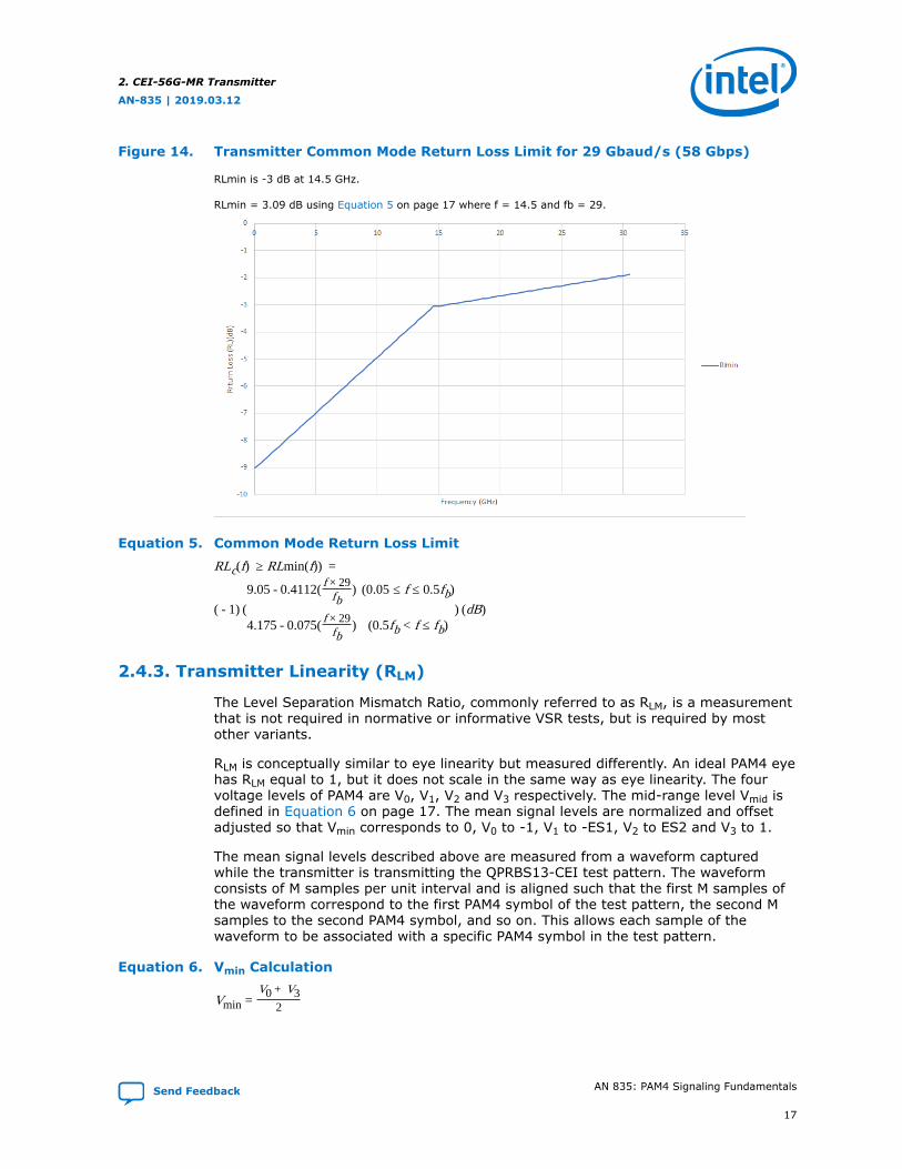
Figure 14. Transmitter Common Mode Return Loss Limit for 29 Gbaud/s (58 Gbps)
RLmin is -3 dB at 14.5 GHz.
RLmin = 3.09 dB using Equation 5 on page 17 where f = 14.5 and fb = 29.
Equation 5. Common Mode Return Loss LimitRLc(f) ≥ RLmin(f)) =
( - 1) (
9.05 - 0.4112(f × 29
fb) (0.05 ≤ f ≤ 0.5fb)
4.175 - 0.075(f × 29
fb) (0.5fb < f ≤ fb)
) (dB)
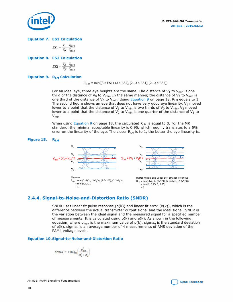
2.4.3. Transmitter Linearity (RLM)
The Level Separation Mismatch Ratio, commonly referred to as RLM, is a measurementthat is not required in normative or informative VSR tests, but is required by mostother variants.
RLM is conceptually similar to eye linearity but measured differently. An ideal PAM4 eyehas RLM equal to 1, but it does not scale in the same way as eye linearity. The fourvoltage levels of PAM4 are V0, V1, V2 and V3 respectively. The mid-range level Vmid isdefined in Equation 6 on page 17. The mean signal levels are normalized and offsetadjusted so that Vmin corresponds to 0, V0 to -1, V1 to -ES1, V2 to ES2 and V3 to 1.
The mean signal levels described above are measured from a waveform capturedwhile the transmitter is transmitting the QPRBS13-CEI test pattern. The waveformconsists of M samples per unit interval and is aligned such that the first M samples ofthe waveform correspond to the first PAM4 symbol of the test pattern, the second Msamples to the second PAM4 symbol, and so on. This allows each sample of thewaveform to be associated with a specific PAM4 symbol in the test pattern.
Equation 6. Vmin Calculation
Vmin =V0 + V3
2
2. CEI-56G-MR Transmitter
AN-835 | 2019.03.12
Send Feedback AN 835: PAM4 Signaling Fundamentals
17
Equation 7. ES1 Calculation
ES1 =V1 - VminV0 - Vmin
Equation 8. ES2 Calculation
ES2 =V2 - VminV3 - Vmin
Equation 9. RLM CalculationRLM = min((3 × ES1), (3 × ES2), (2 - 3 × ES1), (2 - 3 × ES2))
For an ideal eye, three eye heights are the same. The distance of V1 to Vmin is onethird of the distance of V0 to Vmin. In the same manner, the distance of V2 to Vmin isone third of the distance of V3 to Vmin. Using Equation 9 on page 18, RLM equals to 1.The second figure shows an eye that does not have very good eye linearity. V1 movedlower to a point that the distance of V1 to Vmin is two thirds of V0 to Vmin. V2 movedlower to a point that the distance of V2 to Vmin is one quarter of the distance of V3 toVmin.
When using Equation 9 on page 18, the calculated RLM is equal to 0. For the MRstandard, the minimal acceptable linearity is 0.95, which roughly translates to a 5%error on the linearity of the eye. The closer RLM is to 1, the better the eye linearity is.
Figure 15. RLM
2.4.4. Signal-to-Noise-and-Distortion Ratio (SNDR)
SNDR uses linear fit pulse response (p(k)) and linear fit error (e(k)), which is thedifference between the actual transmitter output signal and the ideal signal. SNDR isthe variation between the ideal signal and the measured signal for a specified numberof measurements. It is calculated using p(k) and e(k). As shown in the followingequation, where pmax is the maximum value of p(k), sigmae is the standard deviationof e(k). sigman is an average number of 4 measurements of RMS deviation of thePAM4 voltage levels.
Equation 10.Signal-to-Noise-and-Distortion Ratio
2. CEI-56G-MR Transmitter
AN-835 | 2019.03.12
AN 835: PAM4 Signaling Fundamentals Send Feedback
18

SNDR must be at a minimum 31 dB according to the OIF-56G-MR transmitterspecification.
SNDR is measured at the transmitter output with transmitters on all lanes enabled andtransmitting the QPRBS13-CEI pattern, with at least 14 symbol periods of delaybetween each lane and with identical transmit equalizer settings.
2.5. PAM4 Jitter Methodology
Many NRZ signal standards require extrapolation of Total Jitter (Tj) to BERs of 10-12.This required fitting values to a (dual-dirac) model. Total Jitter (Tj) includes RandomJitter (Rj) and Deterministic Jitter (Dj), which are determined by that extrapolationmethod. PAM4 technologies require only a BER of 10-6 at the physical layer. Sinceoscilloscopes can easily acquire 106 bits in a single acquisition, Rj/Dj extrapolation isnot required, and a new methodology is used for PAM4 signaling.
Table 6. Transmitter Output Jitter Specifications
Characteristic Symbol Condition MIN. TYP. MAX. UNIT
UncorrelatedBounded High
ProbabilityJitter
T_UBHPJ
See (13)
0.05 UIpp
UncorrelatedUnbounded
Gaussian JitterT_UUGJ 0.01 UIrms
Even-Odd Jitter T_EOJ 0.019 UIpp
Uncorrelated Unbounded Gaussian Jitter (UUGJ) is conceptually similar to Rj.Uncorrelated Bounded High Probability Jitter (UBHPJ) is conceptually similar to Dj.Even-Odd Jitter (EOJ) is a new method for PAM4. EOJ is measured from a specificpattern PRBS13Q defined in the OIF-56G standard.
The methodology used to measure UUGJ, UBHPJ and EOJ is defined in section17.3.1.7.1 of the OIF-CEI-56G-MR standard.
2.6. TX Pre-Emphasis Method
When signals travel through a lossy backplane, signal transitions can expand toadjacent intervals. This effect is known as Inter-Symbol Interference (ISI). Thepurpose of TX pre-emphasis is to apply delay and inversion to the signal and add itback to the original signal with the proper weight, thereby compensating for ISI fromthe nearby data symbol.
The transmitter equalization requirements for each CEI standard are defined in theirrespective COM specifications. Refer to CEI-56G-MR-PAM4 Interface Details for moreinformation about transmitter equalization requirements. These are the minimumexpected pre-emphasis requirements. For an MR channel, there are only three taps:
• Main cursor
• Pre-cursor
• Post-cursor
(13) Measured as described in Section 17.3.1.7
2. CEI-56G-MR Transmitter
AN-835 | 2019.03.12
Send Feedback AN 835: PAM4 Signaling Fundamentals
19
Table 7. MR COM Specifications
Parameter Symbol Value Units
Signaling rate fb 18 - 29 Gsym/s
Maximum start frequency fmin 0.05 GHz
Maximum frequency step Δf 0.01 GHz
Device package modelSingle-ended devicecapacitanceTransmission line length,Test 1Transmission line length,Test 2Transmission linecharacteristic impedanceSingle-ended packagecapacitance at package-to-board interface
Cd
zp
zp
ZC
Cp
160123085110
fFmmmmΩfF
Single-ended referenceresistance R0 50 Ω
Single-ended terminationresistance Rd 55 Ω
Receiver 3 dB bandwidth fr 0.75 x fb
Transmitter equalizer,minimum cursor c(0) 0.60 -
Transmitter equalizer, pre-cursor coefficientMinimum valueMaximum valueStep size
c(-1)-0.15
00.05
---
Transmitter equalizer, post-cursor coefficientMinimum valueMaximum valueStep size
c(1)-0.25
00.05
---
Continuous time filter, DCgainMinimum valueMaximum valueStep size
gDC-1501
dBdBdB
Continuous time filter, DCgain2Minimum valueMaximum valueStep size
gDC2-501
dBdBdB
Continuous time filter, zerofrequencies
fzfz2
fb/2.5fb/40
GHzGHz
Continuous time filter, polefrequencies
fp1
fp2
fp3
fb/2.5fb/40
fb
GHzGHz
2. CEI-56G-MR Transmitter
AN-835 | 2019.03.12
AN 835: PAM4 Signaling Fundamentals Send Feedback
20
Related Information
CEI-56G-MR-PAM4 Interface Details on page 22
2. CEI-56G-MR Transmitter
AN-835 | 2019.03.12
Send Feedback AN 835: PAM4 Signaling Fundamentals
21
3. CEI-56G-MR-PAM4 Interface DetailsThis chapter details the electrical interface between nominal baud rates of 18 Gsym/s(36 Gbps) and 29 Gsym/s (58 Gbps) using PAM4 coding.
The signal trace or channel between a transmitter and a receiver must meet theChannel Operating Margin (COM) specification, a method and a threshold quantityused for channel compliance. The COM specification table is normative (mandatory).The insertion loss (IL) or return loss (RL) formulas or graphs are only informative(recommended).
3.1. COM Introduction
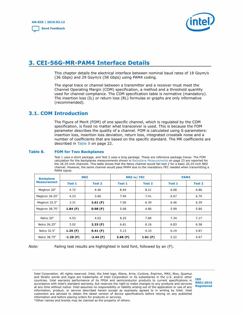
The Figure of Merit (FOM) of one specific channel, which is regulated by the COMspecification, is fixed no matter what transceiver is used. This is because the FOMparameter describes the quality of a channel. FOM is calculated using S-parameters:insertion loss, insertion loss deviation, return loss, integrated crosstalk noise and anumber of coefficients that are based on the specific standard. The MR coefficients aredescribed in Table 8 on page 22.
Table 8. FOM for Two BackplanesTest 1 uses a short package, and Test 2 uses a long package. These are reference package traces. The FOMcalculation for the backplanes measurements shown in Backplane Measurements on page 23 are reported forthe 26.25-inch channels. This table shows that the Nelco channel would fail test 2 for a basic 26.25-inch NRZchannel. However, the same channel would pass PAM4 due to the mandatory FEC needed when transmitting aPAM4 signal.
BackplaneMeasurement
NRZ NRZ w/ FEC PAM4
Test 1 Test 2 Test 1 Test 2 Test 1 Test 2
Megtron 20" 4.72 4.46 8.44 8.21 6.68 6.86
Megtron 26.25" 4.23 3.66 7.94 7.41 6.67 6.70
Megtron 32.5" 3.31 2.61 (F) 7.06 6.39 6.46 6.39
Megtron 38.75" 1.84 (F) 0.98 (F) 5.68 4.86 5.99 5.80
Nelco 20" 4.53 4.02 8.25 7.80 7.34 7.17
Nelco 26.25" 3.02 2.33 (F) 6.81 6.16 6.83 6.58
Nelco 32.5" 1.25 (F) 0.41 (F) 5.13 4.33 6.19 5.87
Nelco 38.75" -1.29 (F) -2.44 (F) 2.66 (F) 1.61 (F) 5.22 4.67
Note: Failing test results are highlighted in bold font, followed by an (F).
AN-835 | 2019.03.12
Send Feedback
Intel Corporation. All rights reserved. Intel, the Intel logo, Altera, Arria, Cyclone, Enpirion, MAX, Nios, Quartusand Stratix words and logos are trademarks of Intel Corporation or its subsidiaries in the U.S. and/or othercountries. Intel warrants performance of its FPGA and semiconductor products to current specifications inaccordance with Intel's standard warranty, but reserves the right to make changes to any products and servicesat any time without notice. Intel assumes no responsibility or liability arising out of the application or use of anyinformation, product, or service described herein except as expressly agreed to in writing by Intel. Intelcustomers are advised to obtain the latest version of device specifications before relying on any publishedinformation and before placing orders for products or services.*Other names and brands may be claimed as the property of others.
ISO9001:2015Registered
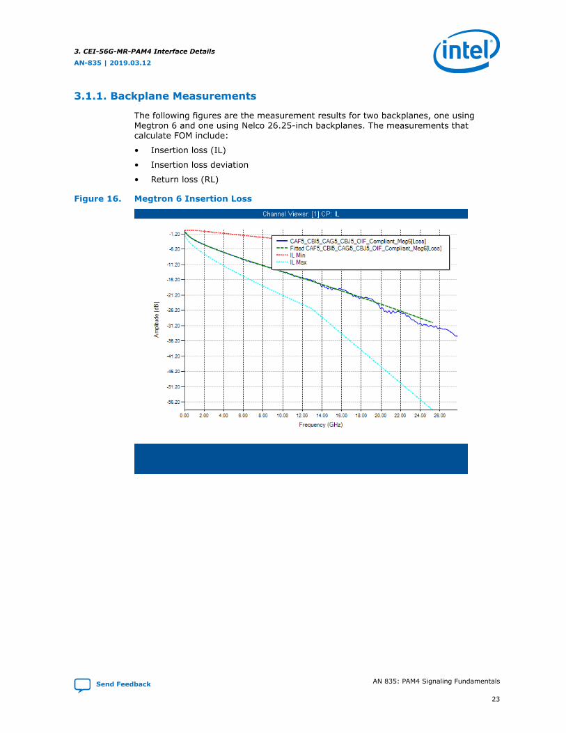
3.1.1. Backplane Measurements
The following figures are the measurement results for two backplanes, one usingMegtron 6 and one using Nelco 26.25-inch backplanes. The measurements thatcalculate FOM include:
• Insertion loss (IL)
• Insertion loss deviation
• Return loss (RL)
Figure 16. Megtron 6 Insertion Loss
3. CEI-56G-MR-PAM4 Interface Details
AN-835 | 2019.03.12
Send Feedback AN 835: PAM4 Signaling Fundamentals
23
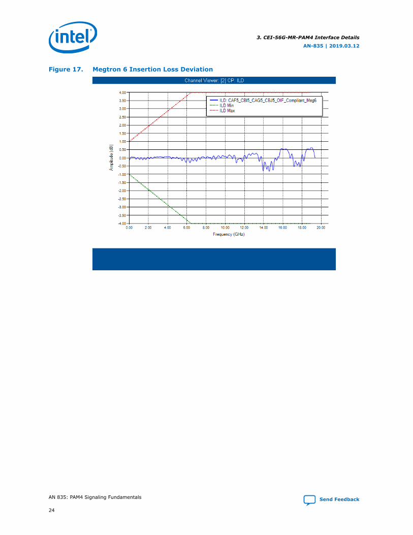
Figure 17. Megtron 6 Insertion Loss Deviation
3. CEI-56G-MR-PAM4 Interface Details
AN-835 | 2019.03.12
AN 835: PAM4 Signaling Fundamentals Send Feedback
24
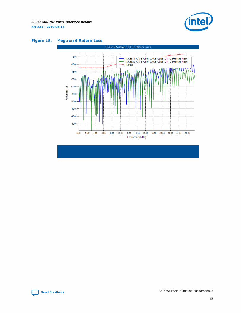
Figure 18. Megtron 6 Return Loss
3. CEI-56G-MR-PAM4 Interface Details
AN-835 | 2019.03.12
Send Feedback AN 835: PAM4 Signaling Fundamentals
25
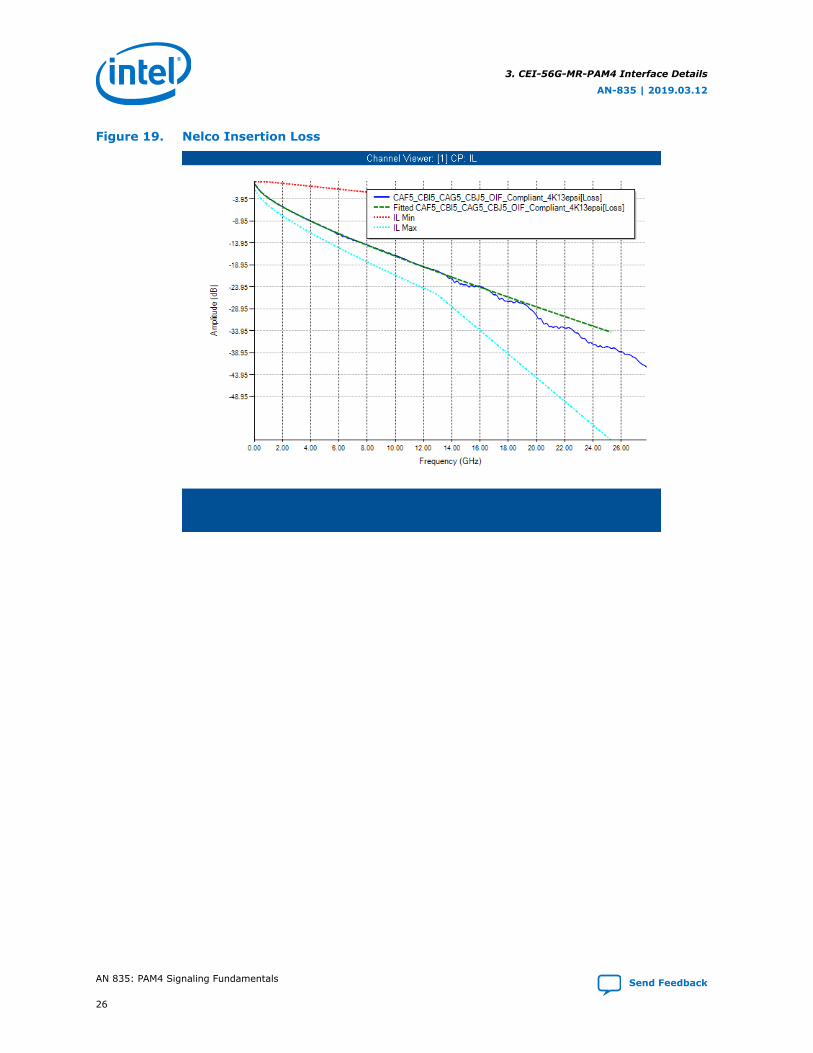
Figure 19. Nelco Insertion Loss
3. CEI-56G-MR-PAM4 Interface Details
AN-835 | 2019.03.12
AN 835: PAM4 Signaling Fundamentals Send Feedback
26
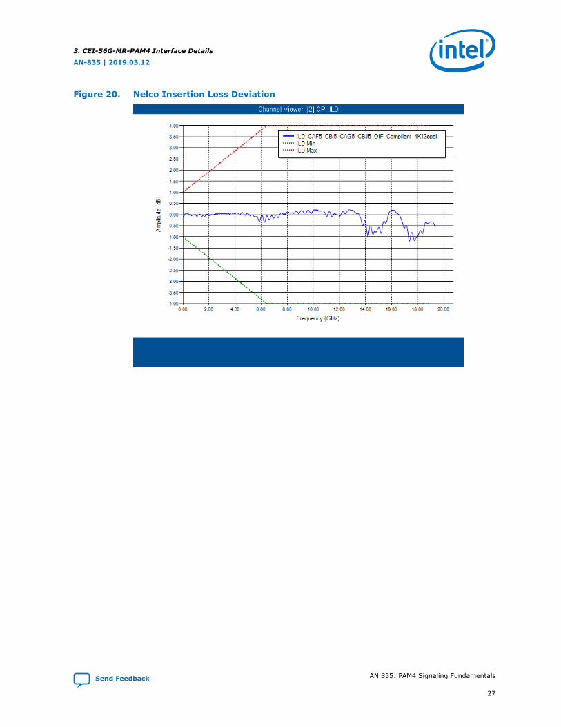
Figure 20. Nelco Insertion Loss Deviation
3. CEI-56G-MR-PAM4 Interface Details
AN-835 | 2019.03.12
Send Feedback AN 835: PAM4 Signaling Fundamentals
27
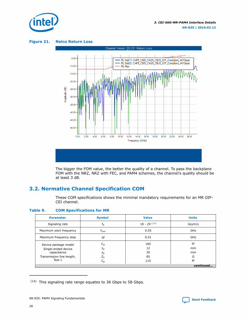
Figure 21. Nelco Return Loss
The bigger the FOM value, the better the quality of a channel. To pass the backplaneFOM with the NRZ, NRZ with FEC, and PAM4 schemes, the channel’s quality should beat least 3 dB.
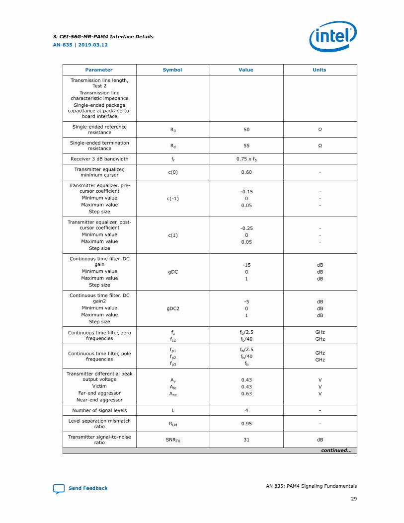
3.2. Normative Channel Specification COM
These COM specifications shows the minimal mandatory requirements for an MR OIF-CEI channel.
Table 9. COM Specifications for MR
Parameter Symbol Value Units
Signaling rate fb 18 - 29 (14) Gsym/s
Maximum start frequency fmin 0.05 GHz
Maximum frequency step Δf 0.01 GHz
Device package modelSingle-ended device
capacitanceTransmission line length,
Test 1
Cd
zp
zp
ZC
Cp
160123085110
fFmmmmΩfF
continued...
(14) This signaling rate range equates to 36 Gbps to 58 Gbps.
3. CEI-56G-MR-PAM4 Interface Details
AN-835 | 2019.03.12
AN 835: PAM4 Signaling Fundamentals Send Feedback
28
Parameter Symbol Value Units
Transmission line length,Test 2
Transmission linecharacteristic impedanceSingle-ended package
capacitance at package-to-board interface
Single-ended referenceresistance R0 50 Ω
Single-ended terminationresistance Rd 55 Ω
Receiver 3 dB bandwidth fr 0.75 x fb
Transmitter equalizer,minimum cursor c(0) 0.60 -
Transmitter equalizer, pre-cursor coefficientMinimum valueMaximum value
Step size
c(-1)-0.15
00.05
---
Transmitter equalizer, post-cursor coefficientMinimum valueMaximum value
Step size
c(1)-0.25
00.05
---
Continuous time filter, DCgain
Minimum valueMaximum value
Step size
gDC-1501
dBdBdB
Continuous time filter, DCgain2
Minimum valueMaximum value
Step size
gDC2-501
dBdBdB
Continuous time filter, zerofrequencies
fzfz2
fb/2.5fb/40
GHzGHz
Continuous time filter, polefrequencies
fp1
fp2
fp3
fb/2.5fb/40
fb
GHzGHz
Transmitter differential peakoutput voltage
VictimFar-end aggressor
Near-end aggressor
Av
Afe
Ane
0.430.430.63
VVV
Number of signal levels L 4 -
Level separation mismatchratio RLM 0.95 -
Transmitter signal-to-noiseratio SNRTX 31 dB
continued...
3. CEI-56G-MR-PAM4 Interface Details
AN-835 | 2019.03.12
Send Feedback AN 835: PAM4 Signaling Fundamentals
29
Parameter Symbol Value Units
Number of samples per unitinterval M 32 -
Decision feedback equalizer(DFE) length Nb 10 UI
Normalized DFE coefficientmagnitude limit for n = 2 to
Nb
bmax(1)bmax(2-Nb)
0.50.2
-
Random jitter, RMS RJ 0.01 UI
Dual-Dirac jitter, peak ADD 0.02 UI
One-sided noise spectraldensity 0 2.6 x 10⁻⁸ V2/GHz
Target detector error ratio DER0 10-6 -
Channel operating margin,min COM 3 dB
A transmitter or receiver must ensure that it meets the values in that table atminimum to be able to claim compliance.
Each standard has a specific table.
3.3. Informative Channel Insertion Loss
For a channel to be considered MR, it must fit within the minimum or maximumenvelope.
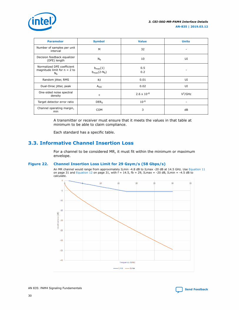
Figure 22. Channel Insertion Loss Limit for 29 Gsym/s (58 Gbps/s)An MR channel would range from approximately ILmin -4.8 dB to ILmax -20 dB at 14.5 GHz. Use Equation 11on page 31 and Equation 12 on page 31, with f = 14.5, fb = 29, ILmax = -20 dB, ILmin = -4.5 dB tocalculate.
3. CEI-56G-MR-PAM4 Interface Details
AN-835 | 2019.03.12
AN 835: PAM4 Signaling Fundamentals Send Feedback
30
Channel insertion loss must be bounded by the following equations:
Equation 11.Maximum Insertion LossILmax =
- [1.083 + 2.398f × 29
fb+ 0.676
f × 29fb
, fmin ≤ f ≤ fb]
Equation 12.Minimum Insertion LossILmin =
- [
0, fmin ≤ 1GHz
13 (f - 1), 1GHz ≤ f ≤ 17.5 GHz
5.5, 17.5 < f ≤ fb
]
3.4. Informative Channel Return Loss
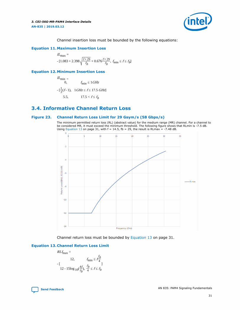
Figure 23. Channel Return Loss Limit for 29 Gsym/s (58 Gbps/s)The minimum permitted return loss (RL) (abstract value) for the medium range (MR) channel. For a channel tobe considered MR, it must exceed the minimum threshold. The following figure shows that RLmin is -7.5 dB.Using Equation 13 on page 31, with f = 14.5, fb = 29, the result is RLmax = -7.48 dB.
Channel return loss must be bounded by Equation 13 on page 31.
Equation 13.Channel Return Loss LimitRLfmax =
- [12, fmin ≤ f
fb4
12 - 15log 10(4ffb
),fb4 ≤ f ≤ fb
]
3. CEI-56G-MR-PAM4 Interface Details
AN-835 | 2019.03.12
Send Feedback AN 835: PAM4 Signaling Fundamentals
31
4. CEI-56G-MR-PAM4 ReceiverThis chapter explains the basic receiver architecture to successfully detect PAM4signals and recover the data with different equalization techniques (when required).
To understand the PAM4 receiver solutions, you should understand the variouschallenges associated with analyzing PAM4 signals.
4.1. Challenges in Analyzing PAM4 Signals
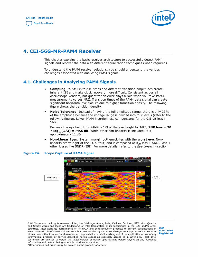
• Sampling Point: Finite rise times and different transition amplitudes createinherent ISI and make clock recovery more difficult. Consistent across alloscilloscope vendors, but quantization error plays a role when you take PAM4measurements versus NRZ. Transition times of the PAM4 data signal can createsignificant horizontal eye closure due to higher transition density. The followingfigure shows the transition density.
• Noise Tolerance: Instead of having the full amplitude range, there is only 33%of the amplitude because the voltage range is divided into four levels (refer to thefollowing figure). Lower PAM4 insertion loss compensates for the 9.5-dB loss inSNR.
Because the eye height for PAM4 is 1/3 of the eye height for NRZ, SNR loss = 20* log10(1/3) = ~9.5 dB. When other non-linearity is included, it isapproximately 11 dB.
• Non-Linear Eyes: System margin bottleneck lies with the worst eye. Non-linearity starts right at the TX output, and is composed of RLM loss + SNDR loss +other losses like SNDR (ISI). For more details, refer to the Eye Linearity section.
Figure 24. Scope Capture of PAM4 Signal
AN-835 | 2019.03.12
Send Feedback
Intel Corporation. All rights reserved. Intel, the Intel logo, Altera, Arria, Cyclone, Enpirion, MAX, Nios, Quartusand Stratix words and logos are trademarks of Intel Corporation or its subsidiaries in the U.S. and/or othercountries. Intel warrants performance of its FPGA and semiconductor products to current specifications inaccordance with Intel's standard warranty, but reserves the right to make changes to any products and servicesat any time without notice. Intel assumes no responsibility or liability arising out of the application or use of anyinformation, product, or service described herein except as expressly agreed to in writing by Intel. Intelcustomers are advised to obtain the latest version of device specifications before relying on any publishedinformation and before placing orders for products or services.*Other names and brands may be claimed as the property of others.
ISO9001:2015Registered
Related Information
Eye Linearity on page 13
4.2. PAM4 Receiver Architecture
While the receiver architecture includes the basic modules required in a PAM4 seriallink, it does not include architectural details of the Intel Stratix 10 PAM4 receiversolution.
4.2.1. Analog vs. Digital Receiver
Transition times of the PAM4 data signal can create significant horizontal eye closuredue to the transition noise, which is dependent on the rise and fall times of the signal.Transition-qualified phase detectors are needed to look at analog levels for clockrecovery.
Legacy NRZ analog receiver design can be leveraged. However, direct detection(comparators for four amplitude levels) requires a lot of power. For multileveltransmission, PAM4, digital receivers prove to be more flexible and provide powerfulsignal processing techniques. This can be expensive because of the addedarchitectural complexities.
4.2.2. Slicer
Unlike NRZ, PAM4 symbols (two bits/symbol) are represented by different voltagelevels. Three slicers with varying voltage thresholds are required to detect thedifferent amplitude levels for PAM4.
4.2.3. Clock and Data Recovery (CDR)
Clock and data recovery is one of the challenging functions in modern high-speedserial data transmission. Multilevel transitions make the NRZ CDR unusable. The mostfamous CDR technique, for PAM4, is baud-rate CDR. Some of the examples are asfollows:
1. Mueller-Mueller phase detector-based CDR
K. Mueller and M. Muller, Timing Recovery in Digital Synchronous Data Receivers,IEEE Transactions on Communications, vol. COM-24, no. 5, pp. 516-531, May1976.
2. Minimum mean square error phase detector-based CDR
E. Lee and D. Messerschmitt, Digital Communication, 2nd ed. Kluwer AcademicPublishers, Massachusetts, 1997.
4.3. Equalization Technique
Channel equalizations are needed to achieve the designated bit error rate targets formost link configurations.
Continuous-time linear equalizer (CTLE), feed-forward equalizer (FFE), and decision-feedback equalizer (DFE) are still the dominant receiver equalization schemes. Most ofthe NRZ equalization techniques are transferable. However, there are certaindistinctions and details that need further attentions in PAM4 signaling links.
4. CEI-56G-MR-PAM4 Receiver
AN-835 | 2019.03.12
Send Feedback AN 835: PAM4 Signaling Fundamentals
33
• Multiple and floating decision threshold levels: The decision thresholds needto be determined adaptively based on the link configuration. This is usually doneby using a dedicated adaptation loop that performs Automatic Gain Control (AGC)on the incoming waveform or adjusts the thresholds based on the statistics of thereceived signal.
• Reduced equalization solution space: In the NRZ scheme, a receiver canusually over-equalize (within certain range) a waveform without dramaticallydecreasing the error-free data recovery margins. Over-equalizing a signal oftensharpens the transition times, which may help reduce the noise-to-jitter transferand, hence, the clock recovery performance. In PAM4, this flexibility is largelytaken away because over-equalization will deteriorate the adjacent symbols. Thisimplies that the equalization needs to be more precise with a reduced solutionspace. Furthermore, the step size of a receiver equalizer with discrete levels, suchas CTLE AC gain levels and FFE/DFE tap coefficients, usually needs to be reducedto achieve the precision goal.
• Receiver nonlinearity effects: Nonlinearity in receivers may introduce non-uniform and asymmetric eye shapes. The equalizer will need to implementcompensation schemes to achieve optimal performance.
The details on receiver equalization are out of the scope of this document. Intel Stratix10 transceivers are auto-adaptive for both NRZ and PAM4 signal recovery.
4.4. CEI-56G-MR-PAM4 Receiver Details
This section details the receiver requirement as per CEI-56G- MR-PAM4 specifications.
A compliant receiver must autonomously operate at the specified bit error rate (BER)with the worst-case combination of a compliant transmitter and a compliant channel.The receiver shall accept the differential input signal amplitudes produced by acompliant transmitter connected with minimum attenuation as specified in Figure 22on page 30.
4.4.1. Electrical Characteristics
Table 10. Receiver Electrical Input Specification for MR
Parameter Symbol Value Unit
Baud Rate R_Baud 18.0 - 29.0 Gsym/s
Differential Input ReturnLoss R_SDD11 Equation 4 on page 16 dB
Differential to CommonMode Input Conversion2 R_SCD11 Equation 11 on page 31 dB
Interference Tolerance See "Receiver Interference Tolerance Parameters" table
Jitter Tolerance See "Receiver Jitter Tolerance Parameters" table
4. CEI-56G-MR-PAM4 Receiver
AN-835 | 2019.03.12
AN 835: PAM4 Signaling Fundamentals Send Feedback
34
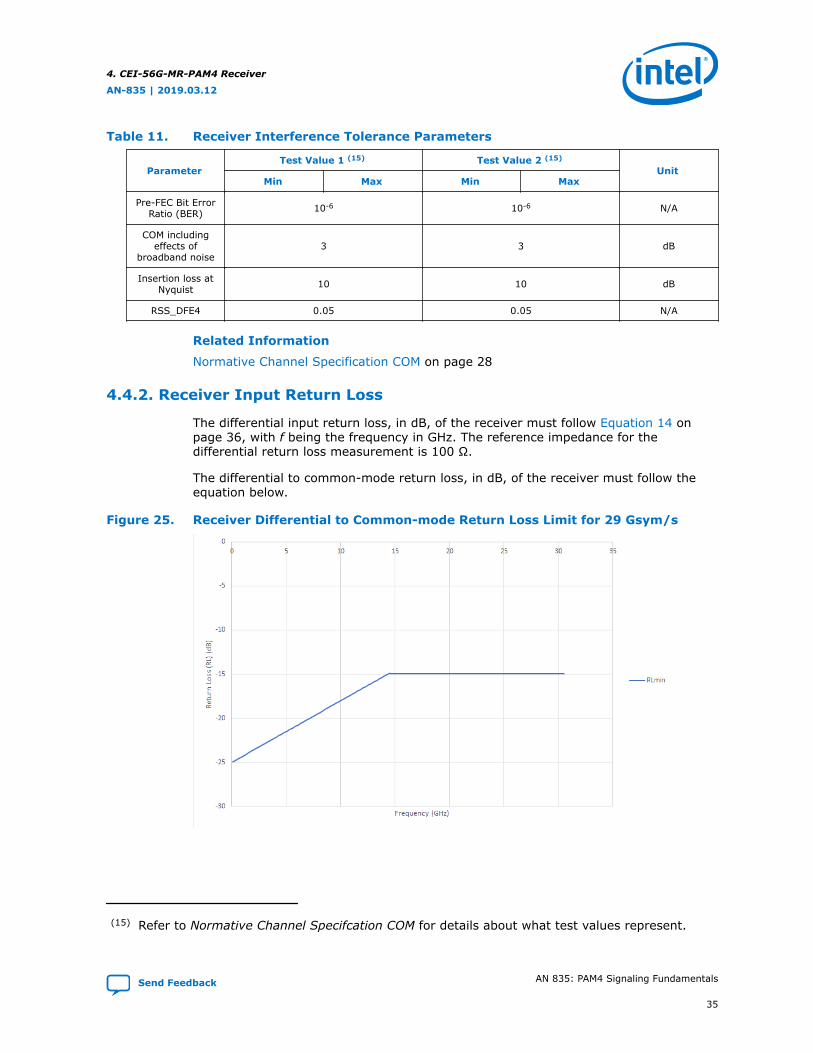
Table 11. Receiver Interference Tolerance Parameters
ParameterTest Value 1 (15) Test Value 2 (15)
UnitMin Max Min Max
Pre-FEC Bit ErrorRatio (BER) 10-6 10-6 N/A
COM includingeffects of
broadband noise3 3 dB
Insertion loss atNyquist 10 10 dB
RSS_DFE4 0.05 0.05 N/A
Related Information
Normative Channel Specification COM on page 28
4.4.2. Receiver Input Return Loss
The differential input return loss, in dB, of the receiver must follow Equation 14 onpage 36, with f being the frequency in GHz. The reference impedance for thedifferential return loss measurement is 100 Ω.
The differential to common-mode return loss, in dB, of the receiver must follow theequation below.
Figure 25. Receiver Differential to Common-mode Return Loss Limit for 29 Gsym/s
(15) Refer to Normative Channel Specifcation COM for details about what test values represent.
4. CEI-56G-MR-PAM4 Receiver
AN-835 | 2019.03.12
Send Feedback AN 835: PAM4 Signaling Fundamentals
35
Equation 14.Differential to Common-Mode Return LossRLdc(f) ≥ RLmin(f) =
( - 1)(25 - 0.6897(
f × 29fb
) (0.05 ≤ f ≤ 0.5fb)
15 (0.5fb < f ≤ fb)) (dB)
4.4.3. Receiver Interference Tolerance
The receiver of each lane must meet the pre-FEC BER requirement with the channelmatching the Channel Operating Margin (COM) and loss parameters for Test 1 andTest 2 (refer to Table 9 on page 28).
The following considerations apply to the interference tolerance test:
• The test transmitter's measured SNDR should be used for SNRTX in the COMcalculation
• The transmitter output levels are set such that RLM is equal to 0.95
• The test transmitter meets the specifications in the CEI-56G-MR Transmittersection.
• The test transmitter is constrained such that for any transmitter equalizer setting,the differential peak-to-peak voltage is less than 800 mV
Related Information
CEI-56G-MR Transmitter on page 11
4.4.4. Receiver Jitter Tolerance
Receiver jitter tolerance must meet the conditions and parameters defined in thefollowing table. This sinusoidal jitter is part of the jitter applied in the stressed inputtest. The receiver BER must be less than the maximum value for each pair of jitterfrequency and peak-to-peak amplitude value listed in the table and figure below.
Table 12. Receiver Jitter Tolerance Parameters
Frequency Range Sinusoidal Jitter, Peak-to-Peak (UI)
f < fb/664000 Not Specified
fb/664000 < f ≤ fb/6640 5 * fb / (664000 * f)
fb/6640 < f ≤ 10 times receiver loop bandwidth (fb/6640) 0.05
4. CEI-56G-MR-PAM4 Receiver
AN-835 | 2019.03.12
AN 835: PAM4 Signaling Fundamentals Send Feedback
36
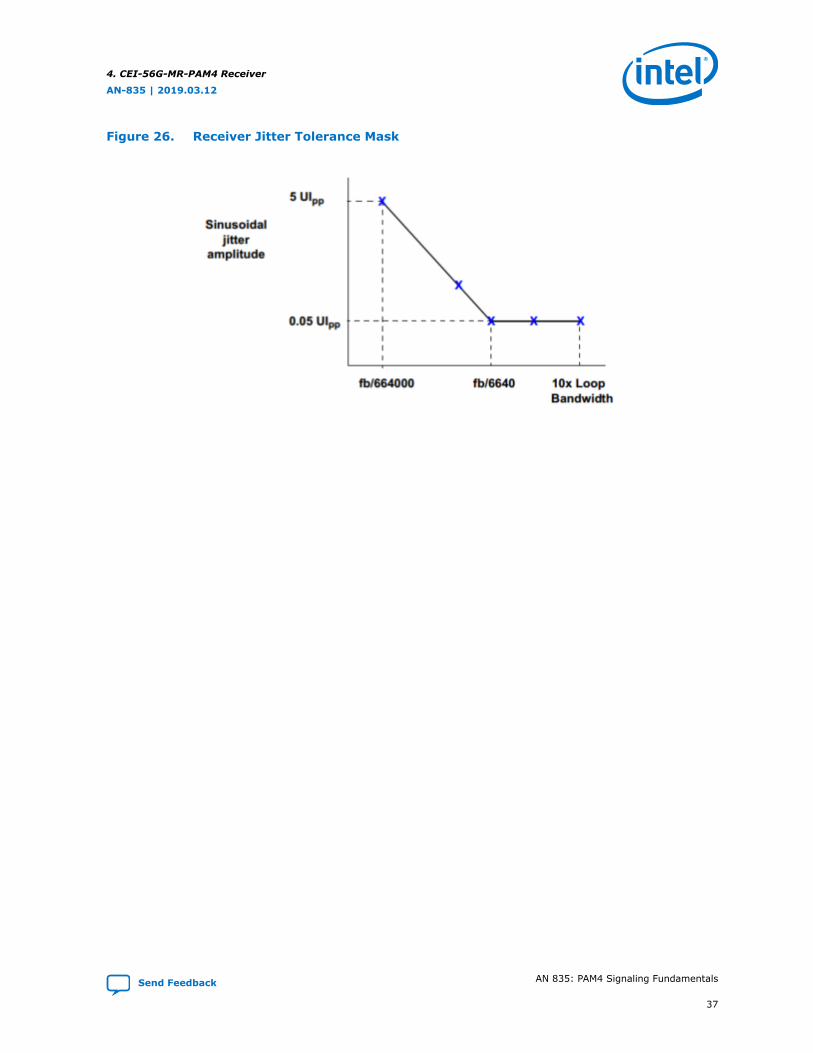
Figure 26. Receiver Jitter Tolerance Mask
4. CEI-56G-MR-PAM4 Receiver
AN-835 | 2019.03.12
Send Feedback AN 835: PAM4 Signaling Fundamentals
37
5. PAM4 Link Case StudyThis section shows the result from a case study on the following two links:
1. OIF_Stressed: Out of spec of CEI-OIF 56G MR spec
2. OIF_Compliant: Within spec of CEI-OIF 56G MR spec
Table 13. Channel Characteristics @ 14 GHz
Electrical Characteristics CEI-56G-MR-PAM4 Spec(dB) OIF_Stressed (dB) OIF_Compliant (dB)
Insertion Loss < 20.0 22.78 18.79
Return Loss > 7.5 ~14.5 ~13.5
Channel Operating Margin(COM) > 3.0 ~3 ~3.7
The link simulations were performed with the help of Intel’s Advanced Link Analyzer.The transmitter and the receiver are both Intel Stratix 10 E-Tile IBIS-AMI models. Thepackage models are added on top because they are not part of the device model.Hence, you observe separate TX and RX package models in the following figures forlink simulation results.
5.1. OIF_Stressed
COM Analysis was run on the channel under test using the Channel Viewer of Intel’sAdvanced Link Analyzer. The COM results were as follows:
• Short package length, COM (test 1) = 3.4139 dB, passing
• Long package length, COM (test 2) = 2.7932 dB, marginally failing
The link simulation was run on the typical TX and RX packages, ~22.6 mm. Thechannel is just passing with COM ~3 dB.
AN-835 | 2019.03.12
Send Feedback
Intel Corporation. All rights reserved. Intel, the Intel logo, Altera, Arria, Cyclone, Enpirion, MAX, Nios, Quartusand Stratix words and logos are trademarks of Intel Corporation or its subsidiaries in the U.S. and/or othercountries. Intel warrants performance of its FPGA and semiconductor products to current specifications inaccordance with Intel's standard warranty, but reserves the right to make changes to any products and servicesat any time without notice. Intel assumes no responsibility or liability arising out of the application or use of anyinformation, product, or service described herein except as expressly agreed to in writing by Intel. Intelcustomers are advised to obtain the latest version of device specifications before relying on any publishedinformation and before placing orders for products or services.*Other names and brands may be claimed as the property of others.
ISO9001:2015Registered
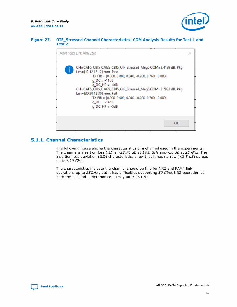
Figure 27. OIF_Stressed Channel Characteristics: COM Analysis Results for Test 1 andTest 2
5.1.1. Channel Characteristics
The following figure shows the characteristics of a channel used in the experiments.The channel’s insertion loss (IL) is ~22.76 dB at 14.0 GHz and~38 dB at 25 GHz. Theinsertion loss deviation (ILD) characteristics show that it has narrow (<2.5 dB) spreadup to ~20 GHz.
The characteristics indicate the channel should be fine for NRZ and PAM4 linkoperations up to 25GHz , but it has difficulties supporting 50 Gbps NRZ operation asboth the ILD and IL deteriorate quickly after 25 GHz.
5. PAM4 Link Case Study
AN-835 | 2019.03.12
Send Feedback AN 835: PAM4 Signaling Fundamentals
39
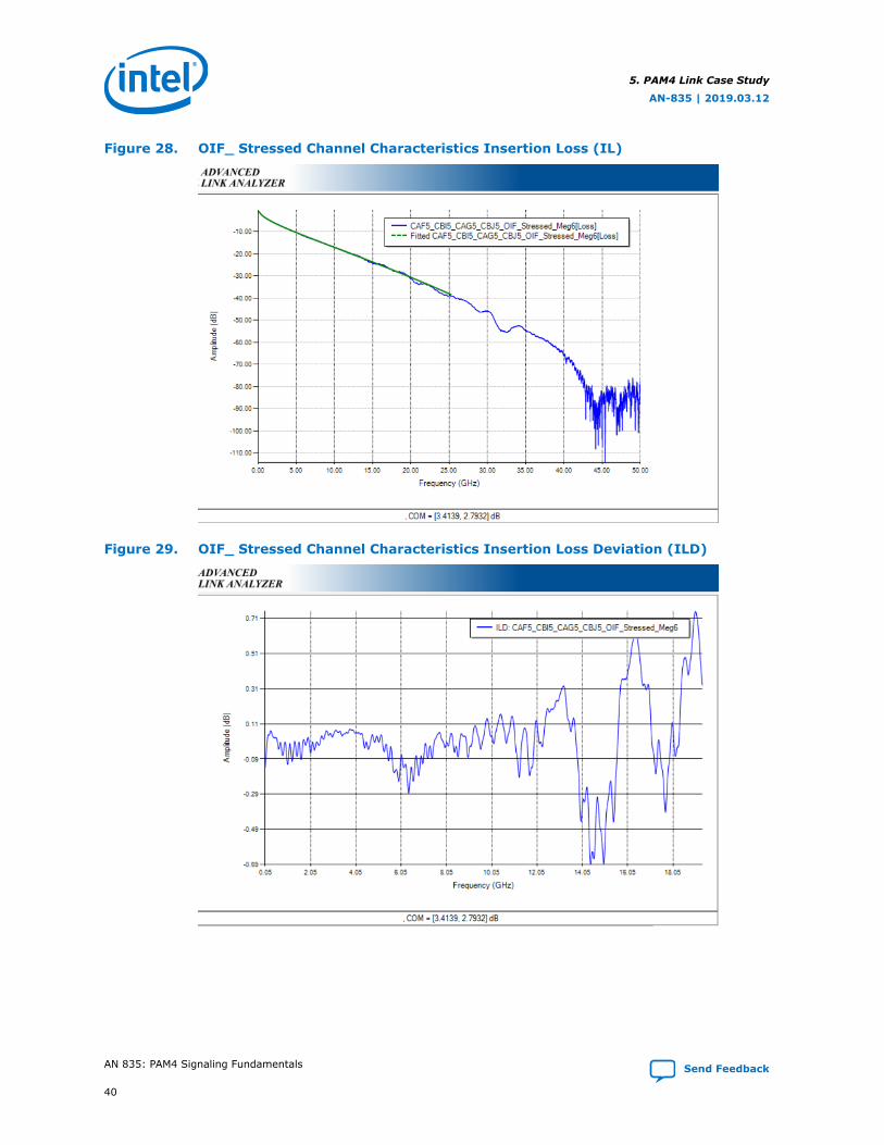
Figure 28. OIF_ Stressed Channel Characteristics Insertion Loss (IL)
Figure 29. OIF_ Stressed Channel Characteristics Insertion Loss Deviation (ILD)
5. PAM4 Link Case Study
AN-835 | 2019.03.12
AN 835: PAM4 Signaling Fundamentals Send Feedback
40
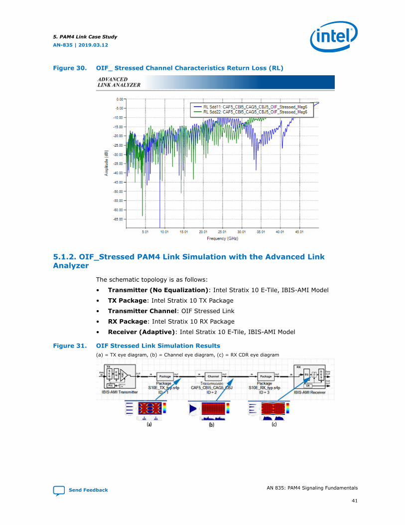
Figure 30. OIF_ Stressed Channel Characteristics Return Loss (RL)
5.1.2. OIF_Stressed PAM4 Link Simulation with the Advanced LinkAnalyzer
The schematic topology is as follows:
• Transmitter (No Equalization): Intel Stratix 10 E-Tile, IBIS-AMI Model
• TX Package: Intel Stratix 10 TX Package
• Transmitter Channel: OIF Stressed Link
• RX Package: Intel Stratix 10 RX Package
• Receiver (Adaptive): Intel Stratix 10 E-Tile, IBIS-AMI Model
Figure 31. OIF Stressed Link Simulation Results(a) = TX eye diagram, (b) = Channel eye diagram, (c) = RX CDR eye diagram
5. PAM4 Link Case Study
AN-835 | 2019.03.12
Send Feedback AN 835: PAM4 Signaling Fundamentals
41
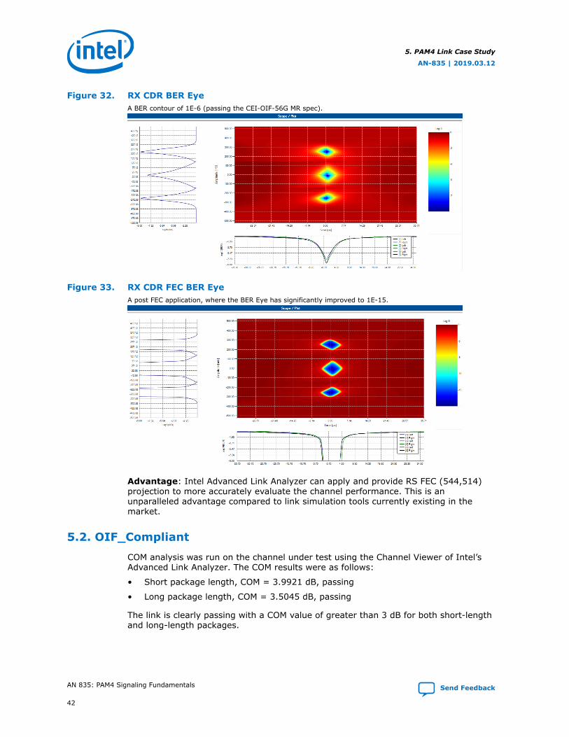
Figure 32. RX CDR BER EyeA BER contour of 1E-6 (passing the CEI-OIF-56G MR spec).
Figure 33. RX CDR FEC BER EyeA post FEC application, where the BER Eye has significantly improved to 1E-15.
Advantage: Intel Advanced Link Analyzer can apply and provide RS FEC (544,514)projection to more accurately evaluate the channel performance. This is anunparalleled advantage compared to link simulation tools currently existing in themarket.
5.2. OIF_Compliant
COM analysis was run on the channel under test using the Channel Viewer of Intel’sAdvanced Link Analyzer. The COM results were as follows:
• Short package length, COM = 3.9921 dB, passing
• Long package length, COM = 3.5045 dB, passing
The link is clearly passing with a COM value of greater than 3 dB for both short-lengthand long-length packages.
5. PAM4 Link Case Study
AN-835 | 2019.03.12
AN 835: PAM4 Signaling Fundamentals Send Feedback
42
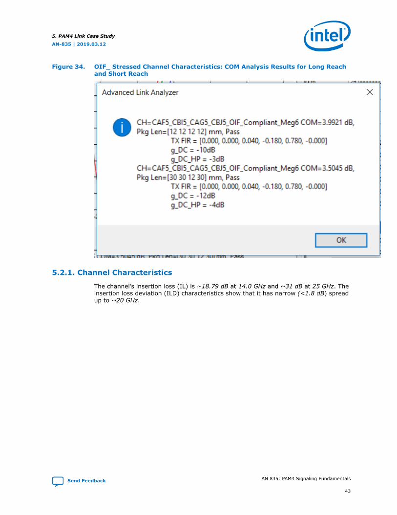
Figure 34. OIF_ Stressed Channel Characteristics: COM Analysis Results for Long Reachand Short Reach
5.2.1. Channel Characteristics
The channel’s insertion loss (IL) is ~18.79 dB at 14.0 GHz and ~31 dB at 25 GHz. Theinsertion loss deviation (ILD) characteristics show that it has narrow (<1.8 dB) spreadup to ~20 GHz.
5. PAM4 Link Case Study
AN-835 | 2019.03.12
Send Feedback AN 835: PAM4 Signaling Fundamentals
43
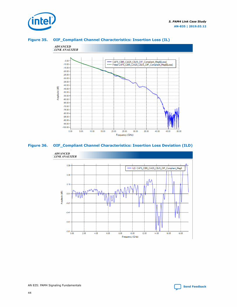
Figure 35. OIF_Compliant Channel Characteristics: Insertion Loss (IL)
Figure 36. OIF_Compliant Channel Characteristics: Insertion Loss Deviation (ILD)
5. PAM4 Link Case Study
AN-835 | 2019.03.12
AN 835: PAM4 Signaling Fundamentals Send Feedback
44
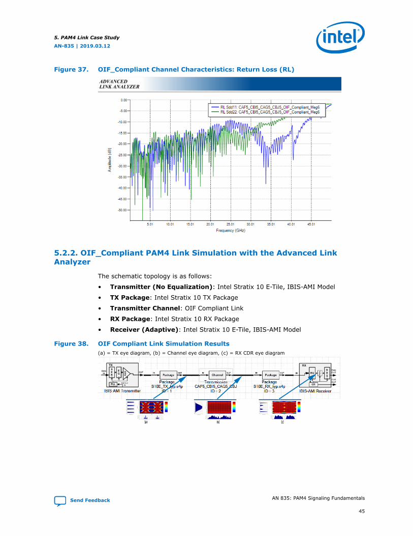
Figure 37. OIF_Compliant Channel Characteristics: Return Loss (RL)
5.2.2. OIF_Compliant PAM4 Link Simulation with the Advanced LinkAnalyzer
The schematic topology is as follows:
• Transmitter (No Equalization): Intel Stratix 10 E-Tile, IBIS-AMI Model
• TX Package: Intel Stratix 10 TX Package
• Transmitter Channel: OIF Compliant Link
• RX Package: Intel Stratix 10 RX Package
• Receiver (Adaptive): Intel Stratix 10 E-Tile, IBIS-AMI Model
Figure 38. OIF Compliant Link Simulation Results(a) = TX eye diagram, (b) = Channel eye diagram, (c) = RX CDR eye diagram
5. PAM4 Link Case Study
AN-835 | 2019.03.12
Send Feedback AN 835: PAM4 Signaling Fundamentals
45
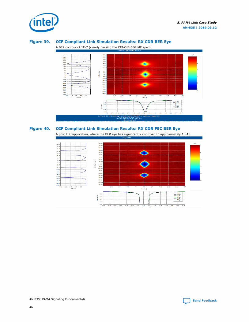
Figure 39. OIF Compliant Link Simulation Results: RX CDR BER EyeA BER contour of 1E-7 (clearly passing the CEI-OIF-56G MR spec).
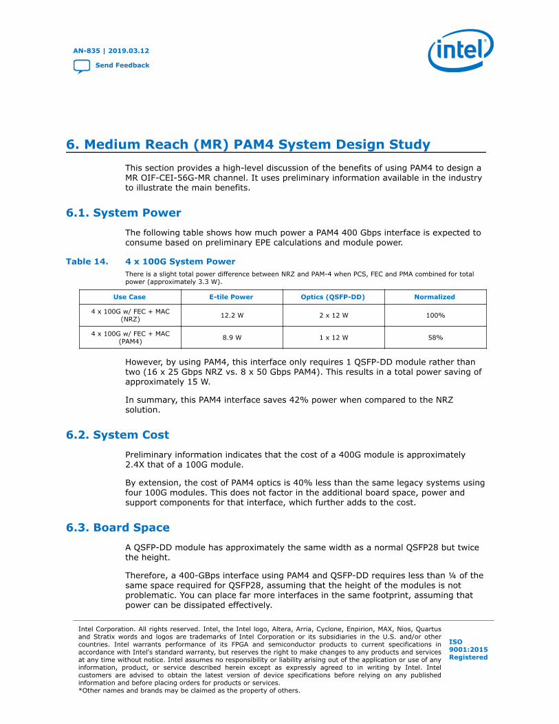
Figure 40. OIF Compliant Link Simulation Results: RX CDR FEC BER EyeA post FEC application, where the BER eye has significantly improved to approximately 1E-18.
5. PAM4 Link Case Study
AN-835 | 2019.03.12
AN 835: PAM4 Signaling Fundamentals Send Feedback
46
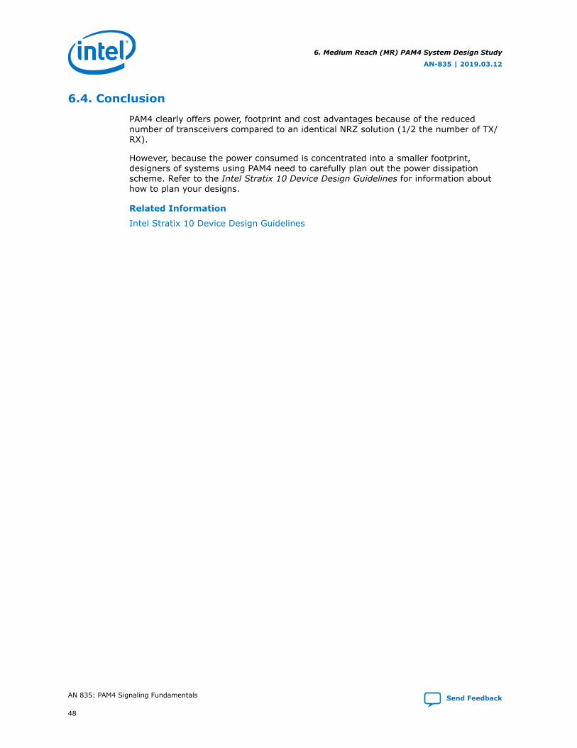
6. Medium Reach (MR) PAM4 System Design StudyThis section provides a high-level discussion of the benefits of using PAM4 to design aMR OIF-CEI-56G-MR channel. It uses preliminary information available in the industryto illustrate the main benefits.
6.1. System Power
The following table shows how much power a PAM4 400 Gbps interface is expected toconsume based on preliminary EPE calculations and module power.
Table 14. 4 x 100G System PowerThere is a slight total power difference between NRZ and PAM-4 when PCS, FEC and PMA combined for totalpower (approximately 3.3 W).
Use Case E-tile Power Optics (QSFP-DD) Normalized
4 x 100G w/ FEC + MAC(NRZ) 12.2 W 2 x 12 W 100%
4 x 100G w/ FEC + MAC(PAM4) 8.9 W 1 x 12 W 58%
However, by using PAM4, this interface only requires 1 QSFP-DD module rather thantwo (16 x 25 Gbps NRZ vs. 8 x 50 Gbps PAM4). This results in a total power saving ofapproximately 15 W.
In summary, this PAM4 interface saves 42% power when compared to the NRZsolution.
6.2. System Cost
Preliminary information indicates that the cost of a 400G module is approximately2.4X that of a 100G module.
By extension, the cost of PAM4 optics is 40% less than the same legacy systems usingfour 100G modules. This does not factor in the additional board space, power andsupport components for that interface, which further adds to the cost.
6.3. Board Space
A QSFP-DD module has approximately the same width as a normal QSFP28 but twicethe height.
Therefore, a 400-GBps interface using PAM4 and QSFP-DD requires less than ¼ of thesame space required for QSFP28, assuming that the height of the modules is notproblematic. You can place far more interfaces in the same footprint, assuming thatpower can be dissipated effectively.
AN-835 | 2019.03.12
Send Feedback
Intel Corporation. All rights reserved. Intel, the Intel logo, Altera, Arria, Cyclone, Enpirion, MAX, Nios, Quartusand Stratix words and logos are trademarks of Intel Corporation or its subsidiaries in the U.S. and/or othercountries. Intel warrants performance of its FPGA and semiconductor products to current specifications inaccordance with Intel's standard warranty, but reserves the right to make changes to any products and servicesat any time without notice. Intel assumes no responsibility or liability arising out of the application or use of anyinformation, product, or service described herein except as expressly agreed to in writing by Intel. Intelcustomers are advised to obtain the latest version of device specifications before relying on any publishedinformation and before placing orders for products or services.*Other names and brands may be claimed as the property of others.
ISO9001:2015Registered
6.4. Conclusion
PAM4 clearly offers power, footprint and cost advantages because of the reducednumber of transceivers compared to an identical NRZ solution (1/2 the number of TX/RX).
However, because the power consumed is concentrated into a smaller footprint,designers of systems using PAM4 need to carefully plan out the power dissipationscheme. Refer to the Intel Stratix 10 Device Design Guidelines for information abouthow to plan your designs.
Related Information
Intel Stratix 10 Device Design Guidelines
6. Medium Reach (MR) PAM4 System Design Study
AN-835 | 2019.03.12
AN 835: PAM4 Signaling Fundamentals Send Feedback
48
7. Glossary and AcronymsTable 15. Glossary of Terms
Terminology Definition
CEI IA A clause-based format supporting publication of new clausesover time
CEI-1.0 Includes CEI-6G-SR, CEI-6G-LR, CEI-11G-SR clauses
CEI-2.0 Added CEI-11G-LR clause
CEI-3.0 Added work from CEI-25G-LR, CEI-28G-SR
CEI-3.1 Includes CEI-28G-MR and CEI-28G-VSR
2.5DA type of die-to-die integration via a silicon interposer
having through-silicon vias (TSVs) connecting its top andbottom metal layers
3D
A three-dimensional (3D) integrated device in which two ormore layers of active electronic components (e.g.,
integrated circuit dies) are integrated vertically into a singlecircuit where through-silicon vias (TSVs) are commonly
used for die-to-die connection
Informative Recommended
Normative Mandatory
Table 16. List of Acronyms
Terminology Definition
AGC Automatic Gain Control
AUI Attachment Unit Interface
CEI Common Electrical Interface
COM Channel Operating Margin
DMT Discrete Multitone Modulation
ENRZ Ensemble Non-Return to Zero
FEC Forward Error Correction
FOM Figure of Merit
IA Implementation Agreements
LR Long Reach
MCM Multi-Chip Module
MR Mid Reach
NRZ Non-Return to Zero
continued...
AN-835 | 2019.03.12
Send Feedback
Intel Corporation. All rights reserved. Intel, the Intel logo, Altera, Arria, Cyclone, Enpirion, MAX, Nios, Quartusand Stratix words and logos are trademarks of Intel Corporation or its subsidiaries in the U.S. and/or othercountries. Intel warrants performance of its FPGA and semiconductor products to current specifications inaccordance with Intel's standard warranty, but reserves the right to make changes to any products and servicesat any time without notice. Intel assumes no responsibility or liability arising out of the application or use of anyinformation, product, or service described herein except as expressly agreed to in writing by Intel. Intelcustomers are advised to obtain the latest version of device specifications before relying on any publishedinformation and before placing orders for products or services.*Other names and brands may be claimed as the property of others.
ISO9001:2015Registered
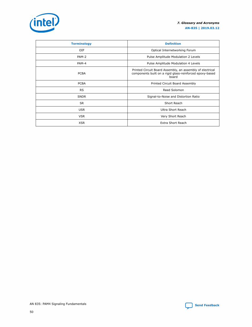
Terminology Definition
OIF Optical Internetworking Forum
PAM-2 Pulse Amplitude Modulation 2 Levels
PAM-4 Pulse Amplitude Modulation 4 Levels
PCBAPrinted Circuit Board Assembly, an assembly of electricalcomponents built on a rigid glass-reinforced epoxy-based
board
PCBA Printed Circuit Board Assembly
RS Reed Solomon
SNDR Signal-to-Noise and Distortion Ratio
SR Short Reach
USR Ultra Short Reach
VSR Very Short Reach
XSR Extra Short Reach
7. Glossary and Acronyms
AN-835 | 2019.03.12
AN 835: PAM4 Signaling Fundamentals Send Feedback
50
8. References1. Equalization and Clock Recovery for a 2.5-10 Gb/s PAM-2/PAM-4 Backplane
Transceiver Cell
2. High Speed Baud-Rate Clock Recovery
3. "Effects of Device Characteristics in Multi-Level Signaling Links"
AN-835 | 2019.03.12
Send Feedback
Intel Corporation. All rights reserved. Intel, the Intel logo, Altera, Arria, Cyclone, Enpirion, MAX, Nios, Quartusand Stratix words and logos are trademarks of Intel Corporation or its subsidiaries in the U.S. and/or othercountries. Intel warrants performance of its FPGA and semiconductor products to current specifications inaccordance with Intel's standard warranty, but reserves the right to make changes to any products and servicesat any time without notice. Intel assumes no responsibility or liability arising out of the application or use of anyinformation, product, or service described herein except as expressly agreed to in writing by Intel. Intelcustomers are advised to obtain the latest version of device specifications before relying on any publishedinformation and before placing orders for products or services.*Other names and brands may be claimed as the property of others.
ISO9001:2015Registered
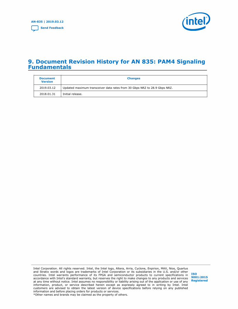
9. Document Revision History for AN 835: PAM4 SignalingFundamentals
DocumentVersion
Changes
2019.03.12 Updated maximum transceiver data rates from 30 Gbps NRZ to 28.9 Gbps NRZ.
2018.01.31 Initial release.
AN-835 | 2019.03.12
Send Feedback
Intel Corporation. All rights reserved. Intel, the Intel logo, Altera, Arria, Cyclone, Enpirion, MAX, Nios, Quartusand Stratix words and logos are trademarks of Intel Corporation or its subsidiaries in the U.S. and/or othercountries. Intel warrants performance of its FPGA and semiconductor products to current specifications inaccordance with Intel's standard warranty, but reserves the right to make changes to any products and servicesat any time without notice. Intel assumes no responsibility or liability arising out of the application or use of anyinformation, product, or service described herein except as expressly agreed to in writing by Intel. Intelcustomers are advised to obtain the latest version of device specifications before relying on any publishedinformation and before placing orders for products or services.*Other names and brands may be claimed as the property of others.
ISO9001:2015Registered