AN-266Circuit Applications of Sample-HoldAmplifiers · TRACE VERTICAL HORIZONTAL A 10V/DIV 1...
14
Application Report SNOA599A – May 2004 – Revised May 2004 AN-266 Circuit Applications of Sample-Hold Amplifiers ..................................................................................................................................................... ABSTRACT Most designers are familiar with the sample-hold amplifier as a system component which is utilized in high speed data acquisition work. In these applications, the sample-hold amplifier is used to store analog data which is then digitized by a relatively slow A/D converter. In this fashion, high speed or multiplexed analog data can be digitized without resorting to complex and expensive ultra-high speed A/D converters. Contents 1 Introduction .................................................................................................................. 2 2 Fiber Optic Data Link Intrusion Alarm .................................................................................... 2 3 Proportional Pulse Stretcher ............................................................................................... 3 4 Controlled Amplitude Pulser ............................................................................................... 5 5 Isolated Input Signal Conditioning Amplifier ............................................................................. 7 6 Precision, High Efficiency Temperature Controller ..................................................................... 9 7 Sample-Hold Amplifier Terms ............................................................................................ 12 List of Figures 1 Fiber Optic Data Link Intrusion Alarm .................................................................................... 2 2 Intrusion Attempt and Detection .......................................................................................... 3 3 Pulse Stretching Circuit .................................................................................................... 4 4 Input Pulse Stretching ...................................................................................................... 5 5 Pulse Amplitude Control Circuit .......................................................................................... 6 6 Pulse Amplitude Control Traces .......................................................................................... 6 7 Isolated Input Signal Conditioning Amplifier ............................................................................. 7 8 Signal Pulses ................................................................................................................ 8 9 Signal Pulses ............................................................................................................... 9 10 Precision, High Efficiency Temperature Controller .................................................................... 10 11 High Gain Amplification Without Drift Problems ....................................................................... 11 12 Controlled Oven Recovers Within 2 seconds After ±0.002°C Steps ............................................... 12 13 Typical Sample-Hold IC Amplifier ....................................................................................... 13 All trademarks are the property of their respective owners. 1 SNOA599A – May 2004 – Revised May 2004 AN-266 Circuit Applications of Sample-Hold Amplifiers Submit Documentation Feedback Copyright © 2004, Texas Instruments Incorporated
Transcript of AN-266Circuit Applications of Sample-HoldAmplifiers · TRACE VERTICAL HORIZONTAL A 10V/DIV 1...

Application ReportSNOA599A–May 2004–Revised May 2004
AN-266 Circuit Applications of Sample-Hold Amplifiers.....................................................................................................................................................
ABSTRACT
Most designers are familiar with the sample-hold amplifier as a system component which is utilized in highspeed data acquisition work. In these applications, the sample-hold amplifier is used to store analog datawhich is then digitized by a relatively slow A/D converter. In this fashion, high speed or multiplexed analogdata can be digitized without resorting to complex and expensive ultra-high speed A/D converters.
Contents1 Introduction .................................................................................................................. 22 Fiber Optic Data Link Intrusion Alarm .................................................................................... 23 Proportional Pulse Stretcher ............................................................................................... 34 Controlled Amplitude Pulser ............................................................................................... 55 Isolated Input Signal Conditioning Amplifier ............................................................................. 76 Precision, High Efficiency Temperature Controller ..................................................................... 97 Sample-Hold Amplifier Terms ............................................................................................ 12
List of Figures
1 Fiber Optic Data Link Intrusion Alarm .................................................................................... 2
2 Intrusion Attempt and Detection .......................................................................................... 3
3 Pulse Stretching Circuit .................................................................................................... 4
4 Input Pulse Stretching ...................................................................................................... 5
5 Pulse Amplitude Control Circuit .......................................................................................... 6
6 Pulse Amplitude Control Traces .......................................................................................... 6
7 Isolated Input Signal Conditioning Amplifier............................................................................. 7
8 Signal Pulses ................................................................................................................ 8
9 Signal Pulses ............................................................................................................... 9
10 Precision, High Efficiency Temperature Controller.................................................................... 10
11 High Gain Amplification Without Drift Problems ....................................................................... 11
12 Controlled Oven Recovers Within 2 seconds After ±0.002°C Steps ............................................... 12
13 Typical Sample-Hold IC Amplifier ....................................................................................... 13
All trademarks are the property of their respective owners.
1SNOA599A–May 2004–Revised May 2004 AN-266 Circuit Applications of Sample-Hold AmplifiersSubmit Documentation Feedback
Copyright © 2004, Texas Instruments Incorporated

Introduction www.ti.com
1 Introduction
Most designers are familiar with the sample-hold amplifier as a system component which is utilized in highspeed data acquisition work. In these applications, the sample-hold amplifier is used to store analog datawhich is then digitized by a relatively slow A/D converter. In this fashion, high speed or multiplexed analogdata can be digitized without resorting to complex and expensive ultra-high speed A/D converters.
The use of sample-hold amplifiers as circuit oriented components is not as common as the class ofapplication described above. This is unfortunate, because sampling techniques allow circuit functionswhich are sophisticated, low cost and not easily achieved with other approaches. An excellent example isfurnished by the fiber optic data link intrusion alarm of Figure 1.
2 Fiber Optic Data Link Intrusion Alarm
The circuit of Figure 1 will detect an attempt to tap a fiber optic data link. It may be used with any fiberoptic communication system which transmits data in pulse coded form. The circuit works by detecting anyshort-term change in the loss characteristics of the fiber optic line. Long term changes due to temperatureand component aging do not affect the circuit. The amplitude of the pulses at the LH0082 fiber opticreceiver IC (A6) will depend upon the characteristics of the photocomponents and the losses in the opticalline. Any attempt to tap the fiber optic will necessitate removal of some amount of light energy. This willcause an instantaneous drop in the pulse amplitude at A6's output. The amplitude of each of A6's outputpulses is sampled by the LF398 sample-hold amplifier (A3), A1 and A2 provide a delayed sample-holdcontrol pulse to A3, which insures that A6's output is sampled well after its output has settled. Undernormal conditions, the pulse-to-pulse amplitude variations at A6's output will be negligible, and the outputof A3 will be at a DC level. A4 is AC coupled and its output will be zero. During an intrusion attempt,energy will be removed from the line and A6's output will shift, causing A3 to jump to a new DC level. Thisshift will be AC amplified by A4 and the A5 comparator will trip, activating the latch circuitry.
Figure 1. Fiber Optic Data Link Intrusion Alarm
2 AN-266 Circuit Applications of Sample-Hold Amplifiers SNOA599A–May 2004–Revised May 2004Submit Documentation Feedback
Copyright © 2004, Texas Instruments Incorporated

www.ti.com Proportional Pulse Stretcher
In Figure 1, fiber optic link eavesdropping attempts are immediately detected by this design. Working on apulse-by-pulse comparison basis, A3 samples each input pulse and holds its output amplitude value at aDC level. Anything that disturbs the next input's amplitude causes a jump in this level; because A4 is anAC-coupled amplifier, the comparator and latch then activate.
Note that the circuit is not affected by slow drifts in circuit components over time and temperature becauseit is only sensitive to AC disturbances on the line. In addition, the frequency and pulse widths of the datamay vary over wide ranges. The photo of an intrusion attempt occurring just past the midpoint of Trace Ais immediately detected by Figure 1's circuit. The photodetector's amplifier output (A) shows a slightamplitude drop. The next time the S-H amplifier samples this signal (B), the alarm latch sets (C). Figure 2shows the circuit in operation. Trace A is A6's output. Trace B is the sample-hold control pin at A3 andTrace C is the latch-alarm output. In this figure, a disturbance on the fiber optic line has occurred just pastthe midpoint of the photo. This is reflected by the reduced amplitude of A6's output at this point. The latch-alarm output goes high just after the sample command rises, due to the sample-hold amplifier jumping tothe new value at A6's output. In the photo, the disturbance has been made large (≃10%) for viewingpurposes. In practice, the circuit will detect an energy removal as small as 0.1% from the line.
Figure 2. Intrusion Attempt and Detection
TRACE VERTICAL HORIZONTAL
A 10V/DIV 1 mSEC/DIV
B 10V/DIV 1 mSEC/DIV
C 10V/DIV 1 mSEC/DIV
3 Proportional Pulse Stretcher
Circuit Figure 3 allows high accuracy measurement of short width pulse durations. The pulses may beeither repetitive or single-shot events. Using digital techniques, a 1% width measurement of a 1 μs eventrequires a 100 MHz clock. This circuit gets around this requirement by linearly amplifying the width of theinput pulse with a time multiplying factor of 1000 or more. Thus, a 1 μs input event will yield a 1 ms outputpulse which is easy to measure to 1%. This measurement capability is useful in high energy physics andnuclear instrumentation work, where short pulse width signals are common. Pulse width measurement
3SNOA599A–May 2004–Revised May 2004 AN-266 Circuit Applications of Sample-Hold AmplifiersSubmit Documentation Feedback
Copyright © 2004, Texas Instruments Incorporated

Proportional Pulse Stretcher www.ti.com
accuracy is enhanced by this pulse stretching circuit. A short input pulse triggers the 74121 one-shot and(via Q1) discharges the 100 pF capacitor while concurrently turning on the recharging current source, Q3.So long as the input pulse is present, the capacitor charges; when the pulse ends, the capacitor's voltageis proportional to the pulse's width. S-H amplifier A2 samples this voltage, and the resultant DC levelcontrols the ON duration of the A4/A5 pulse width modulator.
A sequence of events in Figure 3's circuit stretches a 350 ns input pulse (A) by a factor of 2000. Whentriggered, comparator A1 goes low (B). This action starts the recharging of a capacitor (C) after itspreviously stored charge has been dumped (D). When the input pulse ends, the capacitor's voltage issampled under control of a delayed pulse (E) derived from the input amplifier's inverting output (F). Thesampled and held voltage then turns off a voltage controlled pulse width modulator (G), and a stretchedoutput pulse results (H).
Figure 4, Trace A shows a 350 ns input pulse applied to the circuit of Figure 3. The A1 comparator outputgoes low (Figure 4, Trace B), triggering the DM74121 one shot, which resets the 100 pF capacitor to 0Vvia Q1 with a 50 ns pulse (Trace C). Concurrently, Q2 is turned off, allowing the A3 current source tocharge the 100 pF capacitor in a linear fashion (Figure 4, Trace C). This charging continues until thecircuit input pulse ends, causing A1's output to return high and cutting off the current source. The voltageacross the 100 pF capacitor at this point in time is directly proportional to the width of the circuit inputpulse. This voltage is sampled by the LF398 sample-hold amplifier (A2) which receives its sample-holdcommand from A3 (Figure 4, Trace E—note horizontal scale change at this point). A3 is fed from a delaynetwork which is driven by A1's inverting output. The output of A2 is a DC voltage, which represents thewidth of the most recently applied pulse to the circuit's input. This DC potential is applied to A4, whichalong with A5 comprises a voltage controlled pulse width modulator. A5 ramps positive (Figure 4, TraceG) until it is reset by a pulse from A6, which goes high for a short period (Figure 4, Trace F) each timeA3's output (Figure 4, Trace E) goes low. The ramps at A6's output are compared to A2's output voltageby A4, which goes high for a period linearly dependent on A2's output value (Figure 4, Trace H). Thispulse is the circuit's output.
In this particular circuit, the time amplification factor is about 2000 with a 1 μs full-scale width giving a 1.4ms output pulse. Absolute accuracy of the time expansion is 1% (10 ns) referred to input with resolutiondown to 2 ns. The 50 ns DM74121 reset pulse limits the minimum pulse width the circuit can measure.
Figure 3. Pulse Stretching Circuit
4 AN-266 Circuit Applications of Sample-Hold Amplifiers SNOA599A–May 2004–Revised May 2004Submit Documentation Feedback
Copyright © 2004, Texas Instruments Incorporated

www.ti.com Controlled Amplitude Pulser
Figure 4. Input Pulse Stretching
TRACE VERTICAL HORIZONTAL
A 10V/DIV 100 nSEC/DIV
B 5V/DIV 100 nSEC/DIV
C 5V/DIV 100 nSEC/DIV
D 5V/DIV 100 nSEC/DIV
E 50V/DIV 500 μSEC/DIV
F 50V/DIV 500 μSEC/DIV
G 20V/DIV 500 μSEC/DIV
H 100V/DIV 500 μSEC/DIV
4 Controlled Amplitude Pulser
Pulse amplitude control results when this circuit samples an output pulse's amplitude and compares it witha preset reference level. When the output exceeds this reference, A2 readjusts switching transistor Q3'ssupply voltage to the correct level.Figure 5 depicts a circuit which converts an input pulse train into anamplitude stabilized pulse output which will drive a 20Ω load. The output pulse amplitude is adjustablefrom 0V to 10V and is stable over time, temperature and load changes. This circuit function is useful inautomatic test equipment and general laboratory applications.
The circuit works by storing the sampled amplitude of the output pulse as a DC level, and supplying thisinformation to a feedback loop which controls the voltage applied to the output switch. Each time a pulseis applied at the circuit in- put, the Q2-Q3 combination turns on and drives the load.
5SNOA599A–May 2004–Revised May 2004 AN-266 Circuit Applications of Sample-Hold AmplifiersSubmit Documentation Feedback
Copyright © 2004, Texas Instruments Incorporated

Controlled Amplitude Pulser www.ti.com
Simultaneously, the A1 sample-hold amplifier is placed in the sample mode. When the pulse ends, A1'soutput is at a DC level equal to the amplitude of the output pulse. This level is compared to the amplitudeset DC reference by A2, whose output drives Q1. Q1's emitter provides the DC supply level to the Q2-Q3switch. This servo action forces the amplitude of the output pulse to be the same as the DC potential atthe amplitude set potentiometer wiper, regardless of Q3 switch losses or loading. A 10V, 0.5A pulse (A) isamplitude stabilized by the S-H technique depicted in Figure 5. Note the clean 50 ns rise (B) and fall (C)times. In Figure 6, Trace A is the circuit output. Traces B and C detail the rising and falling edges of theoutput (note horizontal sweep time change for B and C) with clean 50 ns transitions into the 20Ω load.
Figure 5. Pulse Amplitude Control Circuit
Figure 6. Pulse Amplitude Control Traces
TRACE VERTICAL HORIZONTAL
A 10V/DIV 1 mSEC/DIV
B 10V/DIV 100 nSEC/DIV
C 10V/DIV 100 nSEC/DIV
6 AN-266 Circuit Applications of Sample-Hold Amplifiers SNOA599A–May 2004–Revised May 2004Submit Documentation Feedback
Copyright © 2004, Texas Instruments Incorporated
www.ti.com Isolated Input Signal Conditioning Amplifier
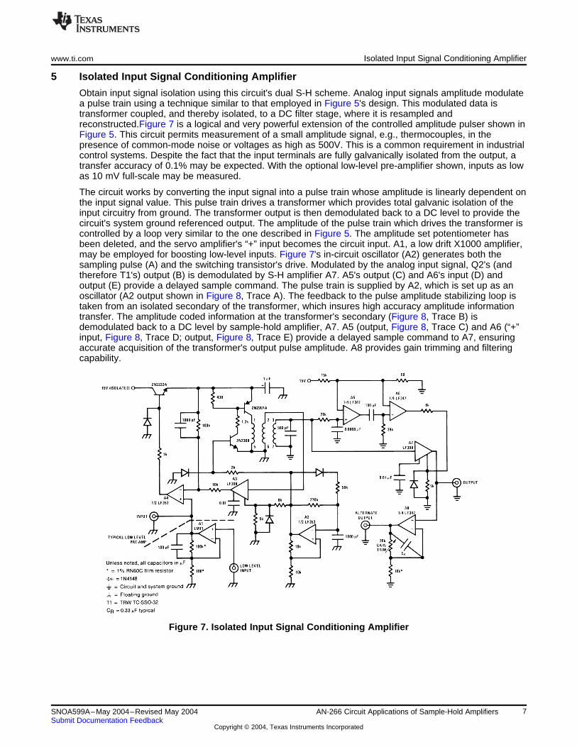
5 Isolated Input Signal Conditioning Amplifier
Obtain input signal isolation using this circuit's dual S-H scheme. Analog input signals amplitude modulatea pulse train using a technique similar to that employed in Figure 5's design. This modulated data istransformer coupled, and thereby isolated, to a DC filter stage, where it is resampled andreconstructed.Figure 7 is a logical and very powerful extension of the controlled amplitude pulser shown inFigure 5. This circuit permits measurement of a small amplitude signal, e.g., thermocouples, in thepresence of common-mode noise or voltages as high as 500V. This is a common requirement in industrialcontrol systems. Despite the fact that the input terminals are fully galvanically isolated from the output, atransfer accuracy of 0.1% may be expected. With the optional low-level pre-amplifier shown, inputs as lowas 10 mV full-scale may be measured.
The circuit works by converting the input signal into a pulse train whose amplitude is linearly dependent onthe input signal value. This pulse train drives a transformer which provides total galvanic isolation of theinput circuitry from ground. The transformer output is then demodulated back to a DC level to provide thecircuit's system ground referenced output. The amplitude of the pulse train which drives the transformer iscontrolled by a loop very similar to the one described in Figure 5. The amplitude set potentiometer hasbeen deleted, and the servo amplifier's “+” input becomes the circuit input. A1, a low drift X1000 amplifier,may be employed for boosting low-level inputs. Figure 7's in-circuit oscillator (A2) generates both thesampling pulse (A) and the switching transistor's drive. Modulated by the analog input signal, Q2's (andtherefore T1's) output (B) is demodulated by S-H amplifier A7. A5's output (C) and A6's input (D) andoutput (E) provide a delayed sample command. The pulse train is supplied by A2, which is set up as anoscillator (A2 output shown in Figure 8, Trace A). The feedback to the pulse amplitude stabilizing loop istaken from an isolated secondary of the transformer, which insures high accuracy amplitude informationtransfer. The amplitude coded information at the transformer's secondary (Figure 8, Trace B) isdemodulated back to a DC level by sample-hold amplifier, A7. A5 (output, Figure 8, Trace C) and A6 (“+”input, Figure 8, Trace D; output, Figure 8, Trace E) provide a delayed sample command to A7, ensuringaccurate acquisition of the transformer's output pulse amplitude. A8 provides gain trimming and filteringcapability.
Figure 7. Isolated Input Signal Conditioning Amplifier
7SNOA599A–May 2004–Revised May 2004 AN-266 Circuit Applications of Sample-Hold AmplifiersSubmit Documentation Feedback
Copyright © 2004, Texas Instruments Incorporated
Isolated Input Signal Conditioning Amplifier www.ti.com
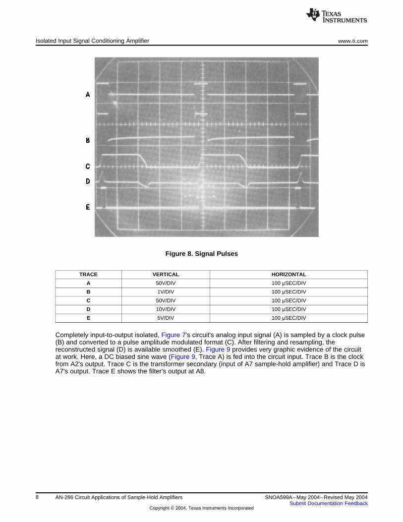
Figure 8. Signal Pulses
TRACE VERTICAL HORIZONTAL
A 50V/DIV 100 μSEC/DIV
B 1V/DIV 100 μSEC/DIV
C 50V/DIV 100 μSEC/DIV
D 10V/DIV 100 μSEC/DIV
E 5V/DIV 100 μSEC/DIV
Completely input-to-output isolated, Figure 7's circuit's analog input signal (A) is sampled by a clock pulse(B) and converted to a pulse amplitude modulated format (C). After filtering and resampling, thereconstructed signal (D) is available smoothed (E). Figure 9 provides very graphic evidence of the circuitat work. Here, a DC biased sine wave (Figure 9, Trace A) is fed into the circuit input. Trace B is the clockfrom A2's output. Trace C is the transformer secondary (input of A7 sample-hold amplifier) and Trace D isA7's output. Trace E shows the filter's output at A8.
8 AN-266 Circuit Applications of Sample-Hold Amplifiers SNOA599A–May 2004–Revised May 2004Submit Documentation Feedback
Copyright © 2004, Texas Instruments Incorporated

www.ti.com Precision, High Efficiency Temperature Controller
Figure 9. Signal Pulses
TRACE VERTICAL HORIZONTAL
A 5V/DIV 100 mSEC/DIV
B 100V/DIV
C 5V/DIV
D 5V/DIV
E 5V/DIV
6 Precision, High Efficiency Temperature Controller
Tight temperature control results when high voltage pulses synchronously drive a thermistor-bridge—atrick that increases signal level—and are then sampled and used to control a pulse width modulatedheater driver. The sample-hold amplifier in Figure 10 is used to provide very high stability in an oventemperature control circuit. In this circuit, the output signal of the pulse driven thermistor-bridge is tentimes greater than the usual DC driven bridge. In thermistor-bridges, power dissipation in the resistors andthermistor is the limiting factor in how much DC bridge drive may be used. However, if the bridge drive isapplied in the form of high voltage pulses at very low duty cycle, average power dissipation will be low anda high bridge output signal will result.
9SNOA599A–May 2004–Revised May 2004 AN-266 Circuit Applications of Sample-Hold AmplifiersSubmit Documentation Feedback
Copyright © 2004, Texas Instruments Incorporated

Precision, High Efficiency Temperature Controller www.ti.com
Figure 10. Precision, High Efficiency Temperature Controller
In Figure 10, this operation is implemented by having the A1 oscillator drive Q1 to energize a common24V transformer used “backwards”. The transformer's floated output is a 100V pulse which is applieddirectly across the thermistor-bridge. With one side of the bridge output grounded, the bridge drive withrespect to ground appears as complementary 50V pulses (Figure 11, Traces A and B). A2 providesamplification of the bridge's pulsed output (Figure 11, Trace C). A3, a sample-hold amplifier, samples themiddle of A2's output pulses and has a DC output equal to the amplitude of these pulses. Proper timingfor A3's sample command (Figure 11, Trace D) is provided by the A4-A5 pair and their associated RCnetworks. The DC output of A3 is low-pass filtered and fed to A6, which combines with A7 to form asimple pulse width modulator. The output of A7 is a ramp (Figure 11, Trace F—note horizontal scalechange) which is periodically reset by A5's output (Figure 11, Trace E). This ramp is compared at A6 toA3's output, and the resultant pulse at A6's output (Figure 11, Trace G) is used to drive the Q2 heatercontrol switch. In this fashion, the ON time of the pulse applied to the heater will be proportional to thesensed offset at the thermistor-bridge. Thermal feedback from the heater to the thermistor completes aloop around the circuit. The 5 MΩ potentiometer is used to adjust the time constant of this loop, and the2.5k potentiometer at A2 sets the gain.
Driving a thermistor-bridge with complementary high voltage pulses (A and B) permits high gainamplification without drift problems (C). Driven by a delayed sample command (D), a S-H amplifierconverts the bridge's error signal to a DC level (E) that controls a pulse width modulated heater driver (Fand G).
In operation, with the thermistor and heater tightly coupled, the time constant of the loop is adjusted byapplying small step changes in the temperature setpoint. This is done by alternately opening and closing aswitch across a 100Ω resistor in series with one of the bridge resistors. For the thermistor shown, thisrepresents a 0.02°C step. The response of the loop to these steps can be monitored at A3's output. Withthe loop time constant and gain properly adjusted, A3's output will settle in a minimum amount of time inresponse to the steps. Figure 12 shows settling for both “+” and “−” steps, with settling inside 2 secondsfor either polarity step.
10 AN-266 Circuit Applications of Sample-Hold Amplifiers SNOA599A–May 2004–Revised May 2004Submit Documentation Feedback
Copyright © 2004, Texas Instruments Incorporated

www.ti.com Precision, High Efficiency Temperature Controller
Figure 11. High Gain Amplification Without Drift Problems
TRACE VERTICAL HORIZONTAL
A 100V/DIV 200 μSEC/DIV
B 100V/DIV 200 μSEC/DIV
C 5V/DIV 200 μSEC/DIV
D 10V/DIV 200 μSEC/DIV
E 5V/DIV 1 mSEC/DIV
F 10V/DIV 1 mSEC/DIV
G 50V/DIV 1 mSEC/DIV
11SNOA599A–May 2004–Revised May 2004 AN-266 Circuit Applications of Sample-Hold AmplifiersSubmit Documentation Feedback
Copyright © 2004, Texas Instruments Incorporated

Sample-Hold Amplifier Terms www.ti.com
Figure 12. Controlled Oven Recovers Within 2 seconds After ±0.002°C Steps
In Figure 12, tight heater to thermistor coupling and careful calibration can provide rapid temperaturerestabilization. Here the controlled oven recovers within 2 seconds after ±0.002°C steps.
Once adjusted, and driving a well insulated and designed oven, the circuit's control stability can bemonitored. The high output signal levels from the bridge, in combination with the gain provided by A2,yield extremely good performance.
7 Sample-Hold Amplifier Terms
Acquisition Time: The time required to acquire a new analog input voltage with an output step of 10V.Note that acquisition time is not just the time required for the output to settle, but also includes the timerequired for all internal nodes to settle so that the output assumes the proper value when switched to thehold mode.
Aperture Time: The delay required between hold command and an input analog transition, so that thetransition does not affect the held output.
Dynamic Sampling Error: The error introduced into the held output due to a changing analog input at thetime the hold command is given. Error is expressed in mV with a given hold capacitor value and input slewrate. Note that this error term occurs even for long sample times.
Gain Error: The ratio of output voltage swing to input voltage swing in the sample mode expressed as apercent difference.
Hold Settling Time: The time required for the output to settle within 1 mV of final value after the holdlogic command.
Hold Step: The voltage step at the output of the sample-hold when switching from sample mode to holdmode with a steady (DC) analog input voltage. Logic swing is specified, usually 5V.
12 AN-266 Circuit Applications of Sample-Hold Amplifiers SNOA599A–May 2004–Revised May 2004Submit Documentation Feedback
Copyright © 2004, Texas Instruments Incorporated

www.ti.com Sample-Hold Amplifier Terms
Figure 13. Typical Sample-Hold IC Amplifier
13SNOA599A–May 2004–Revised May 2004 AN-266 Circuit Applications of Sample-Hold AmplifiersSubmit Documentation Feedback
Copyright © 2004, Texas Instruments Incorporated

IMPORTANT NOTICE
Texas Instruments Incorporated and its subsidiaries (TI) reserve the right to make corrections, enhancements, improvements and otherchanges to its semiconductor products and services per JESD46, latest issue, and to discontinue any product or service per JESD48, latestissue. Buyers should obtain the latest relevant information before placing orders and should verify that such information is current andcomplete. All semiconductor products (also referred to herein as “components”) are sold subject to TI’s terms and conditions of salesupplied at the time of order acknowledgment.
TI warrants performance of its components to the specifications applicable at the time of sale, in accordance with the warranty in TI’s termsand conditions of sale of semiconductor products. Testing and other quality control techniques are used to the extent TI deems necessaryto support this warranty. Except where mandated by applicable law, testing of all parameters of each component is not necessarilyperformed.
TI assumes no liability for applications assistance or the design of Buyers’ products. Buyers are responsible for their products andapplications using TI components. To minimize the risks associated with Buyers’ products and applications, Buyers should provideadequate design and operating safeguards.
TI does not warrant or represent that any license, either express or implied, is granted under any patent right, copyright, mask work right, orother intellectual property right relating to any combination, machine, or process in which TI components or services are used. Informationpublished by TI regarding third-party products or services does not constitute a license to use such products or services or a warranty orendorsement thereof. Use of such information may require a license from a third party under the patents or other intellectual property of thethird party, or a license from TI under the patents or other intellectual property of TI.
Reproduction of significant portions of TI information in TI data books or data sheets is permissible only if reproduction is without alterationand is accompanied by all associated warranties, conditions, limitations, and notices. TI is not responsible or liable for such altereddocumentation. Information of third parties may be subject to additional restrictions.
Resale of TI components or services with statements different from or beyond the parameters stated by TI for that component or servicevoids all express and any implied warranties for the associated TI component or service and is an unfair and deceptive business practice.TI is not responsible or liable for any such statements.
Buyer acknowledges and agrees that it is solely responsible for compliance with all legal, regulatory and safety-related requirementsconcerning its products, and any use of TI components in its applications, notwithstanding any applications-related information or supportthat may be provided by TI. Buyer represents and agrees that it has all the necessary expertise to create and implement safeguards whichanticipate dangerous consequences of failures, monitor failures and their consequences, lessen the likelihood of failures that might causeharm and take appropriate remedial actions. Buyer will fully indemnify TI and its representatives against any damages arising out of the useof any TI components in safety-critical applications.
In some cases, TI components may be promoted specifically to facilitate safety-related applications. With such components, TI’s goal is tohelp enable customers to design and create their own end-product solutions that meet applicable functional safety standards andrequirements. Nonetheless, such components are subject to these terms.
No TI components are authorized for use in FDA Class III (or similar life-critical medical equipment) unless authorized officers of the partieshave executed a special agreement specifically governing such use.
Only those TI components which TI has specifically designated as military grade or “enhanced plastic” are designed and intended for use inmilitary/aerospace applications or environments. Buyer acknowledges and agrees that any military or aerospace use of TI componentswhich have not been so designated is solely at the Buyer's risk, and that Buyer is solely responsible for compliance with all legal andregulatory requirements in connection with such use.
TI has specifically designated certain components which meet ISO/TS16949 requirements, mainly for automotive use. Components whichhave not been so designated are neither designed nor intended for automotive use; and TI will not be responsible for any failure of suchcomponents to meet such requirements.
Products Applications
Audio www.ti.com/audio Automotive and Transportation www.ti.com/automotive
Amplifiers amplifier.ti.com Communications and Telecom www.ti.com/communications
Data Converters dataconverter.ti.com Computers and Peripherals www.ti.com/computers
DLP® Products www.dlp.com Consumer Electronics www.ti.com/consumer-apps
DSP dsp.ti.com Energy and Lighting www.ti.com/energy
Clocks and Timers www.ti.com/clocks Industrial www.ti.com/industrial
Interface interface.ti.com Medical www.ti.com/medical
Logic logic.ti.com Security www.ti.com/security
Power Mgmt power.ti.com Space, Avionics and Defense www.ti.com/space-avionics-defense
Microcontrollers microcontroller.ti.com Video and Imaging www.ti.com/video
RFID www.ti-rfid.com
OMAP Applications Processors www.ti.com/omap TI E2E Community e2e.ti.com
Wireless Connectivity www.ti.com/wirelessconnectivity
Mailing Address: Texas Instruments, Post Office Box 655303, Dallas, Texas 75265Copyright © 2012, Texas Instruments Incorporated