Simulation Methods of Quantum-Dot Semiconductor Optical Amplifiers

1
The Basics of Testing Operation Amplifiers: Three Methods
Presenter: David R. Baum Co Author: Daryl Hiser
Date: 23April2008

2 2
Purpose
• This paper will provide information on three operational amplifier test methods which have a proven track record.
• Frequently we get questions about how to test opamps. This paper will serve as a teaching tool that we can use to help people quickly learn the various methods.
• The presentation will discuss the tradeoffs and how to make the best test circuit choice.

3 3
Test Method Outline • Overview of the three test circuits. • Iq (Quiescent Current) • Vos (Input Offset Voltage) • PSRR (Power Supply Rejection Ratio) • CMRR (Common Mode Rejection Ratio) • Ib, Ios (Input Bias Current, Input Offset Current) • Aol (DC Open Loop Gain) • Putting it all together

4 4
Method 1 – Self Test Circuit
• The “Self Test” method uses the DUT itself to perform the test. It is sometimes called the false summing junction method.
50k
50k Rin
50
1001*Vos
+Vs
Vs Iq Figure 3, False Summing Junction
Rf 50k
Vout DUT
+
Vin
Vos +
_ _

5 5
Method 1 Self Test Circuit
• Advantages – Simplicity of design – Most stable of the three methods
• Disadvantages – Can be slower – Low Iq parts are difficult to test
Continued

6 6
Method 2 – Two Amp Loop
• The “Two Amp Loop” method uses another “Loop Amplifier” to perform the tests.
Vout
Loop Amp + DUT
+
Rin
50
50k Rf
+Vs
Vs
Iq Figure 4
=1001*Vos

7 7
Method 2 – Two Amp Loop
• Advantages – Accurate control of DUT output voltage – Usually faster testing
• Disadvantages – Stability – Compensation must be correct – Not useful for DUTs with variable gain/phase
Continued

8 8
Method 3 – Three Amp Loop
• The “Three Amp Loop” method uses two additional amplifier to perform the tests.
+ +
Loop Control
+
Iq Figure 5, Buffer Loop (Three Amp)
Loop Amp
Vout
1Meg
500k
1Meg
+
DUT
Rin
50
50k Rf
+Vs
Vs

9 9
Method 3 – Three Amp Loop
• Advantages – Accurate control of DUT output voltage – Usually faster testing – DUT power supplies can be > Loop amps
• Disadvantages – Stability – Compensation must be correct – Not useful for DUTs with variable gain/phase – There is always a 1Meg load on the DUT
Continued

10 10
Iq (Quiescent Current) • Definition the current consumed by the part with the output current equal to zero
+Vs
Vs
+
DUT
Iq Figure 1
• This circuit satisfies this requirement. Ib will generally be very small and not contribute any significant error to the quiescent current measurement. However, this circuit doesn’t allow testing other device parameters and is therefore not very useful.

11 11
Iq (Quiescent Current) • This circuit is more practical, but still only allows two parameters to be easily tested.
Rf 50k
Vs
+Vs
+
DUT
50 Rin
Iq Figure 2, Self Test
Vos +
_ 1001*Vos
Continued

12
Iq (Quiescent Current) Figure 3 represents a more practical circuit for measuring the quiescent current in very low quiescent current parts. In this implementation the output can be adjusted to zero output current by controlling Vin, not always and easy task
50k
50k Rin
50
1001*Vos
+Vs
Vs Iq Figure 3, False Summing Junction
Rf 50k
Vout DUT
+
Vin
Vos +
_ _
Continued

13
Iq (Quiescent Current)
The three amp loop in Figure 5 can also be used to measure Iq, but care must be taken as there is always a 1 Meg ohm resistor at the output of the DUT.
Continued
+ +
Loop Control
+
Iq Figure 5, Buffer Loop (Three Amp)
Loop Amp
Vout
1Meg
500k
1Meg
+
DUT
Rin
50
50k Rf
+Vs
Vs
a1

Slide 13
a1 The three amp loop in Figure 5 can also be used to measure Iq, but care must be taken as there is always a 1 Meg ohm resistor at the output of the DUT. a0873033, 4/7/2008
14
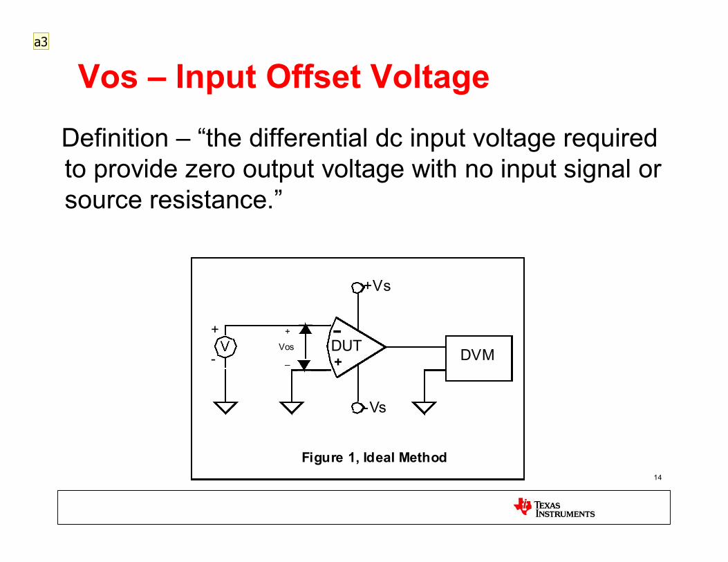
Vos – Input Offset Voltage
Definition – “the differential dc input voltage required to provide zero output voltage with no input signal or source resistance.”
+ V DVM
Vs
+Vs
Figure 1, Ideal Method
DUT +
Vos
+
_
a3
Slide 14
a3 The Input Offset Voltage, Vos, is variously defined as, “the differential dc input voltage required to provide zero output voltage with no input signal or source resistance,” or “the differential dc input voltage require to provide zero output voltage, with no other input signal and zero resistance in either input terminal path to ground,” or “the differential dc input voltage required to provide zero voltage at the output of an operational amplifier when the input bias current is zero.” This would suggest an “ideal” theoretical method for testing the Input Offset Voltage which is impractical. The definition would suggest that one should connect a low output, variable voltage source with high accuracy and resolution to the input of the operational amplifier and adjust the input voltage until the output voltage is zero. Then the input offset voltage would simply be the inverse of the input voltage applied. There are two serious problems with this method. With operational amplifiers with very high open loop gain, the resolution of the voltage source would have to be less than a microvolt to guarantee any degree of repeatability and an iterative approach would need to be used to drive the output to zero. This would be costly in time if it could ever be achieved. Noise in the system, coupling into the voltage source and operational amplifier, would make the measurement and control next to impossible in a high speed automated test environment. Graeme, Jerald G., Tobey, Gene E., Huelsman, Lawrence P., "Operational Amplifers, Design and Applications", McGraw Hill Book Company, New York, p 454, 1971 Wait, John V., Huelsman, Lawrence P., Korn, Granino A., ôIntroduction to Operational Amplifier Theory and Applications,ö McGraw Hill Book Company, New York, p 101, 1975
a0873033, 4/7/2008
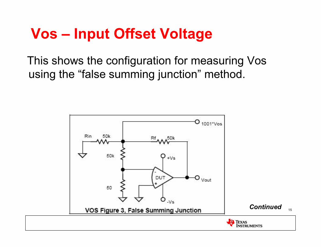
15
Vos – Input Offset Voltage
This shows the configuration for measuring Vos using the “false summing junction” method.
Continued

16
Vos – Input Offset Voltage
Offset voltage is easy to measure with the two amplifier loop.
Continued

17
Vos – Input Offset Voltage
The three amplifier loop must be kept stable by the appropriate selection of resistor and capacitor on the far right amplifier.
Continued

18
Vos – Input Offset Voltage “Errors”
Sources of error may not be obvious!
Continued

19
Vos – Input Offset Voltage “Errors”
This shows sources of error due to Thermal EMF.
Continued

20
Vos – Input Offset Voltage “Errors” A. Thermally Generated EMFs caused by:
– Relay Contacts – Solder Joints – SWAP Block Pogo Pin Connections – Automated handler contacts and sockets.
B. Leakage currents caused by: – Power Supplies – Relay Control and supply traces.
C. Noise – Environment – Testers – components, for example: resistor noise
Continued

21
Practical Design Considerations for Test Boards

22
Practical Design Considerations for Test Boards
Continued

23
PSRR Power Supply Rejections Ratio
Definition the ratio of the absolute value of the change in the supply voltages divided by the change in the input offset voltage of the op amp. Simply it is Operational Amplifiers ability to reject changes in the power supply voltages over a specified range. Since the offset voltage is needed to make this measurement, the techniques already developed for measuring Vos can be used.
Continued

24
PSRR Power Supply Rejections Ratio
This test can be accomplished in all three test loop circuits by setting the power supplies, +Vs and Vs to the minimum supply voltage for the DUT. Then measure 1001 * Vos. The supplies should then be programmed to the maximum voltage for the DUT. Then measure 1001*Vos again. Now we can calculate PSRR.
Continued

25
PSRR Power Supply Rejections Ratio
Measuring PSRR with this method is the same as the selftest loop.
Continued

26
PSRR Power Supply Rejections Ratio
PSRR Equations
Continued

27
CMRR Common Mode Rejections Ratio
Definition the ratio of the differential voltage gain to the commonmode voltage gain. It is the op amp’s ability to reject common mode voltages over a specified range. Since the offset voltage is needed to make this measurement, the techniques already developed for measuring Vos can be used

28
CMRR Common Mode Rejections Ratio
The CMRR measurement with the two amp loop is made the same way as the selftest loop method.

29
CMRR Common Mode Rejections Ratio
CMRR Equations
Continued
a6

Slide 29
a6 It may be desirable to make all measurements with respect to ground. This can be accomplished by keeping the noninverting input tied to ground, and moving the power supplies in a tracking fashion positively or negatively to apply effective common mode voltages to the amplifier. The output must be driven to the midpoint of the supplies to eliminate any Aol errors to corrupt the CMRR measurement using this technique. a0873033, 4/11/2008

30
Ib+ Input Bias Current
An+ electrometer can be used in this configuration because the amplifier is stable.

31
Ib Input Bias Current
Ib, which is usually hard to measure, can be measured with an electrometer in this configuration because the loop amp keeps the DUT stable.
Continued

32
Ib Input Bias Current
Continued

33
Ib Input Bias Current
Continued

34
Ib Input Bias Current
Continued

35
Ib Input Bias Current
Continued

36
Ib Input Bias Current
Continued

37
Ib Input Bias Current
Continued

38
Ib Input Bias Current
Continued

39
Aol – DC Open Loop Gain

40
Aol – DC Open Loop Gain
Continued

41
Aol – DC Open Loop Gain
Continued

42
Aol – DC Open Loop Gain
Continued

43
Aol – DC Open Loop Gain
Continued

44 44
Putting it all together
The nice thing about the “SelfTest” method and the “Two Amp Loop” is that they can live together easily on the same test board.
• Advantages –Stability is never an issue –Both methods can be used on the same part –Comparison is easy.
• Disadvantage –Requires more board space / components –Requires more programming

45 45
Putting it all together – Two Amp
Continued

46 46
Putting it all together – Self Test
Continued

47 47
Conclusions

48 48
Method 1 Self Test Circuit
• Advantages – Simplicity of design – Most stable of the three methods
• Disadvantages – Can be slower – Low Iq parts are difficult to test
Continued

49 49
Method 2 – Two Amp Loop
• Advantages – Accurate control of DUT output voltage – Usually faster testing
• Disadvantages – Stability – Compensation must be correct – Not useful for DUTs with variable gain/phase
Continued

50 50
Method 3 – Three Amp Loop
• Advantages – Accurate control of DUT output voltage – Usually faster testing – DUT power supplies can be > Loop amps
• Disadvantages – Stability – Compensation must be correct – Not useful for DUTs with variable gain/phase – There is always a 1Meg load on the DUT
Continued