Amplifier-Based Tuneable RF Predistortion for Radio-over ...
95
Amplifier-Based Tuneable RF Predistortion for Radio-over-Fibre Systems Jingfang Liu A Thesis In the Department of Electrical and Computer Engineering Presented in Partial Fulfillment of the Requirements for the Degree of Master of Applied Science (Electrical and Computer Engineering) at Concordia University Montréal, Québec, Canada March 2011 Jingfang Liu, 2011
Transcript of Amplifier-Based Tuneable RF Predistortion for Radio-over ...

Amplifier-Based Tuneable RF Predistortion for
Radio-over-Fibre Systems
Jingfang Liu
A Thesis
In the Department
of
Electrical and Computer Engineering
Presented in Partial Fulfillment of the Requirements
for the Degree of Master of Applied Science (Electrical and Computer Engineering) at
Concordia University
Montréal, Québec, Canada
March 2011
Jingfang Liu, 2011
CONCORDIA UNIVERSITY
SCHOOL OF GRADUATE STUDIES
This is to certify that the thesis prepared
By: Jingfang Liu
Entitled: “Amplifier-based Tuneable RF Predistortion for Radio-over-Fiber
Systems”
and submitted in partial fulfillment of the requirements for the degree of
Master of Applied Science
Complies with the regulations of this University and meets the accepted standards with
respect to originality and quality.
Signed by the final examining committee:
________________________________________________ Chair
Dr. D. Qiu
________________________________________________ Examiner, External
Dr. A. Ben Hamza, CIISE To the Program
________________________________________________ Examiner
Dr. P. Valizadeh
________________________________________________ Supervisor
Dr. G. Cowan
________________________________________________ Supervisor
Dr. X. Zhang
Approved by: ___________________________________________
Dr. W. E. Lynch, Chair
Department of Electrical and Computer Engineering
____________20_____ ___________________________________
Dr. Robin A. L. Drew
Dean, Faculty of Engineering and
Computer Science

iii
ABSTRACT
Amplifier-Based Tuneable RF Predistortion for Radio-over-Fibre Systems
Jingfang Liu
Semiconductor laser diodes (LDs) have been extensively employed for directly
transporting wideband multicarrier signals in radio-over-fibre (RoF) systems. However,
an inherent characteristic of LDs, the nonlinearity, always has been a fundamental
problem in fibre-optic systems. When optical subcarrier modulation (SCM) is used,
nonlinear characteristics will induce harmonic and intermodulation distortion (IMD)
products that degrade the system’s performance significantly. Therefore, it is essential to
improve the linearity of RoF systems.
An amplifier-based tuneable radio frequency (RF) predistortion circuit for RoF
systems is proposed to linearize the distributed feedback laser diode (DFB-LD) in the
range of 0.7 ~ 2.5 .GHz Instead of conventional insertion loss linearization techniques, in
this work, a high gain amplifier-based tuneable predistortion circuit was designed. The
designed amplifier-based predistortion circuit consists of an impedance matching
network and a distortion generation block. To match the distortion generator to the 50
characteristic impedance of an RF source, a capacitively cross-coupled common gate
(CCC-CG) broadband matching network is designed. The tuneability of the predistortion
circuit is achieved by adjusting the bias current of the triplet-core circuit in the
predistortion generation block. The predistortion integrated circuit (IC) is designed with
TSMC90nm technology. Performance of the investigated predistortion is simulated with
Cadence Virtuoso Hspice/Spectre circuit simulator. Compared with free running LDs,

iv
this predistortion circuit achieves more than 10 dB third-order IMD (IMD3) suppression
over the operating frequency range. The proposed scheme is suitable for broadband RF
optical transmission applications.
Theoretical analysis of the nonlinear transfer function of the predistortion circuit
and DFB-LD has been performed. The nonlinearity of transistors under different
configurations is analyzed.

v
Acknowledgements
I would like to thank many people who made my life at Concordia memorable
and enjoyable. First and foremost, I wish to acknowledge my advisors Dr. X. Zhang and
Dr. G. Cowan-they are great research mentors who gave me strong motivation in my
research. I really appreciate the opportunity they provided and their considerate guidance,
patient advice and support for me to finish this work.
I want to thank Dr. B. Hraimel for performing the measurement, PhD candidate
Frank Bernardo and VLSI/CAD Specialist Ted Obuchowicz for their help with CAD
tools. Thanks to my friends in photonics lab and VLSI lab for their helpful discussions
with optical components, CAD tools and friendship.
Also I have sincere appreciation to the Le Fonds québécois de la recherche sur la
nature et les technologies (FQRNT), Quebec, Canada for supporting this research project.
Finally, I must reserve my special thanks for my significant others. I would like to
thank my parents, my sister, brother and my husband Luo Ma for their unconditional love
and support throughout my life.

vi
Table of Contents
ABSTRACT ...................................................................................................................... iii
Acknowledgements ........................................................................................................... v
Table of Contents ............................................................................................................. vi
List of Figures ................................................................................................................... ix
List of Tables ................................................................................................................... xii
List of Acronyms ............................................................................................................ xiii
List of Principal Symbols .............................................................................................. xvi
Chapter 1 Introduction..................................................................................................... 1
1.1 Introduction .......................................................................................................................... 1
1.2 Motivation and Review of Technologies ............................................................................ 3
1.3 Objective ............................................................................................................................... 8
1.4 Thesis Scope and Contributions ......................................................................................... 9
1.5 Thesis Outline ..................................................................................................................... 10
Chapter 2 The Principle of Predistortion ..................................................................... 12
2.1 Introduction to Distributed Feedback Laser Diode ........................................................ 12
2.2 Mathematical Analysis of Predistortion........................................................................... 13
2.2.1 Modeling of Nonlinear Transmission Characteristics of a DFB-LD in RoF Systems .. 14
2.2.2 Mathematical Analysis of Predistortion ........................................................................ 17
2.3 Triplet-Core Circuit ........................................................................................................... 20
2.3.1 Nonlinear Transconductance of a Single Transistor and Differential Circuits ............. 21
2.3.2 Introduction of Gilbert Cell and the Multi-tanh Principle ............................................ 26
2.3.3 Proposed Triplet-Core Circuit....................................................................................... 28

vii
2.4 Conclusion ........................................................................................................................... 33
Chapter 3 Input Impedance Matching Network Design of The Proposed Triplet-
core Circuit ...................................................................................................................... 34
3.1 Introduction ........................................................................................................................ 34
3.2 Capacitively Cross-coupled Common Gate LNA ............................................................ 35
3.2.1 Noise Analysis of the CCC-CG LNA ........................................................................... 40
3.2.2 S-parameter Test Setup of Fully Differential Circuit.................................................... 41
3.2.3 Design and Simulation Results ..................................................................................... 42
3.3 Nonlinearity Analysis of the CG LNA and CCC-CG LNA ............................................ 45
3.5 Conclusion .......................................................................................................................... 47
Chapter 4 Design of the Amplifier-based Tuneable RF Predistortion ...................... 48
4.1 Introduction ........................................................................................................................ 48
4.2 Design Guidelines of the Amplfier-Based Tuneable RF Predistortion Circuit ............ 48
4.2.1 System Architecture Consideration .............................................................................. 49
4.2.2 Current Mirror Design .................................................................................................. 51
4.2.2.1 Basic Current Mirror .................................................................................. 52
4.2.2.2 Cascode Current Mirror ............................................................................. 53
4.2.2.3 Active Current Mirror ................................................................................ 55
4.2.3 Current Injection Technique ......................................................................................... 57
4.2.4 Laser Bias Circuit and Output Stage Power Supply ..................................................... 58
4.3 Circuit Performance Evaluation ....................................................................................... 59
4.3.1 Two-Tone Signal Simulation ........................................................................................ 59
4.3.2 Tuneability Evaluation .................................................................................................. 65
4.4 Comparison of This Work with Previous Predistortion ................................................. 67

viii
4.5 Conclusion .......................................................................................................................... 68
Chapter 5 Conclusion ..................................................................................................... 70
5.1 Conclusion .......................................................................................................................... 70
5.2 Future Work ....................................................................................................................... 71
References ........................................................................................................................ 73

ix
List of Figures
Figure 1.1 Radio-over-fibre system [1]............................................................................................ 2
Figure 1.2 Mixed polarization linearization of MZM for OSSB modulation [4]. ........................... 4
Figure 1.3 Diagram of a feedforward system [6]. ............................................................................ 5
Figure 1.4 Predistortion block diagram [7]. ..................................................................................... 7
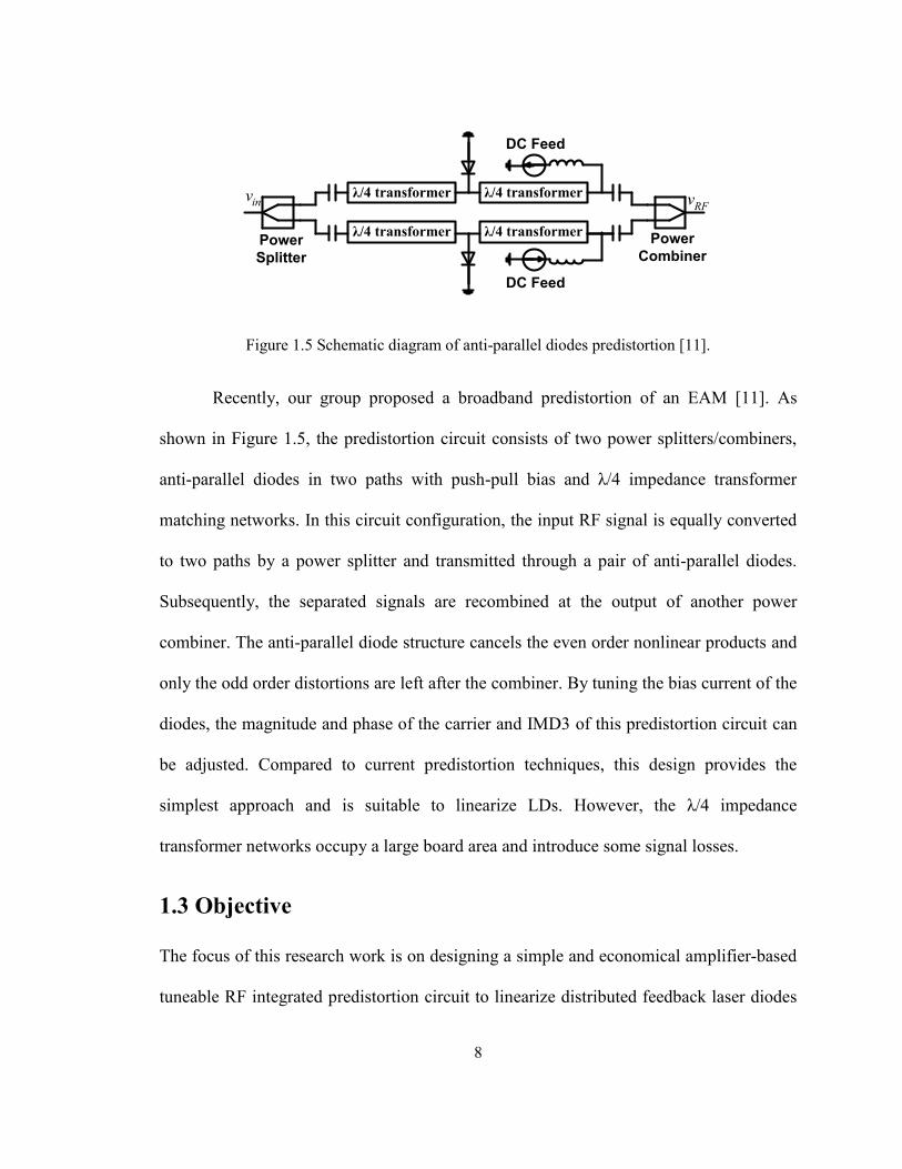
Figure 1.5 Schematic diagram of anti-parallel diodes predistortion [11]. ....................................... 8
Figure 2.1 Diagram of a DFB-LD with Bragg grating on the top [12]. ......................................... 13
Figure 2.2 Measured nonlinear characteristics of a DFB-LD. ....................................................... 14
Figure 2.3 Measured nonlinear characteristics of the DFB-LD. .................................................... 16
Figure 2.4 Block diagram of predistortion circuit and DFB-LD. .................................................. 17
Figure 2.5 Desired gm curve of the predistortion circuit. ............................................................... 19
Figure 2.6 Nonlinear characteristic of DFB-LD with theoretical predistortion cancellation. ........ 20
Figure 2.7 Simulated DC characteristics of a W/L (10 µm/100 nm) NMOSFET. ........................ 22
Figure 2.8 Simulated g2/g1 and g3/g1 ratio of a W/L (10 µm/100 nm) NMOSFET. ...................... 22
Figure 2.9 Basic differential pair. .................................................................................................. 23
Figure 2.10 Voltage-current (V-I) characteristic of the differential pair. ...................................... 25
Figure 2.11 gm of transistor M1. ..................................................................................................... 25
Figure 2.12 Basic Multi-tanh doublet [21]. .................................................................................... 27
Figure 2.13 Dual gm components for the doublet. .......................................................................... 28
Figure 2.14 Transconductance of the proposed doublet circuit. .................................................... 29
Figure 2.15 Schematic diagram of the proposed triplet-core circuit. ............................................. 30
Figure 2.16 gm curves of proposed triplet-core circuit. .................................................................. 31
Figure 2.17 Overall gm curves by tuning I1 and I3. ......................................................................... 32

x
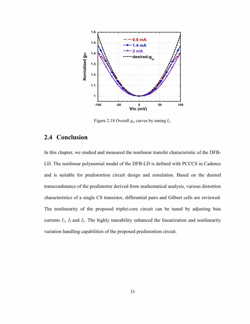
Figure 2.18 Overall gm curves by tuning I2. ................................................................................... 33
Figure 3.1 Basic CG LNA. ............................................................................................................ 36
Figure 3.2 Dominant noise sources in the basic CG LNA [29]. .................................................... 37
Figure 3.3 Proposed fully differential CCC-CG LNA. .................................................................. 38
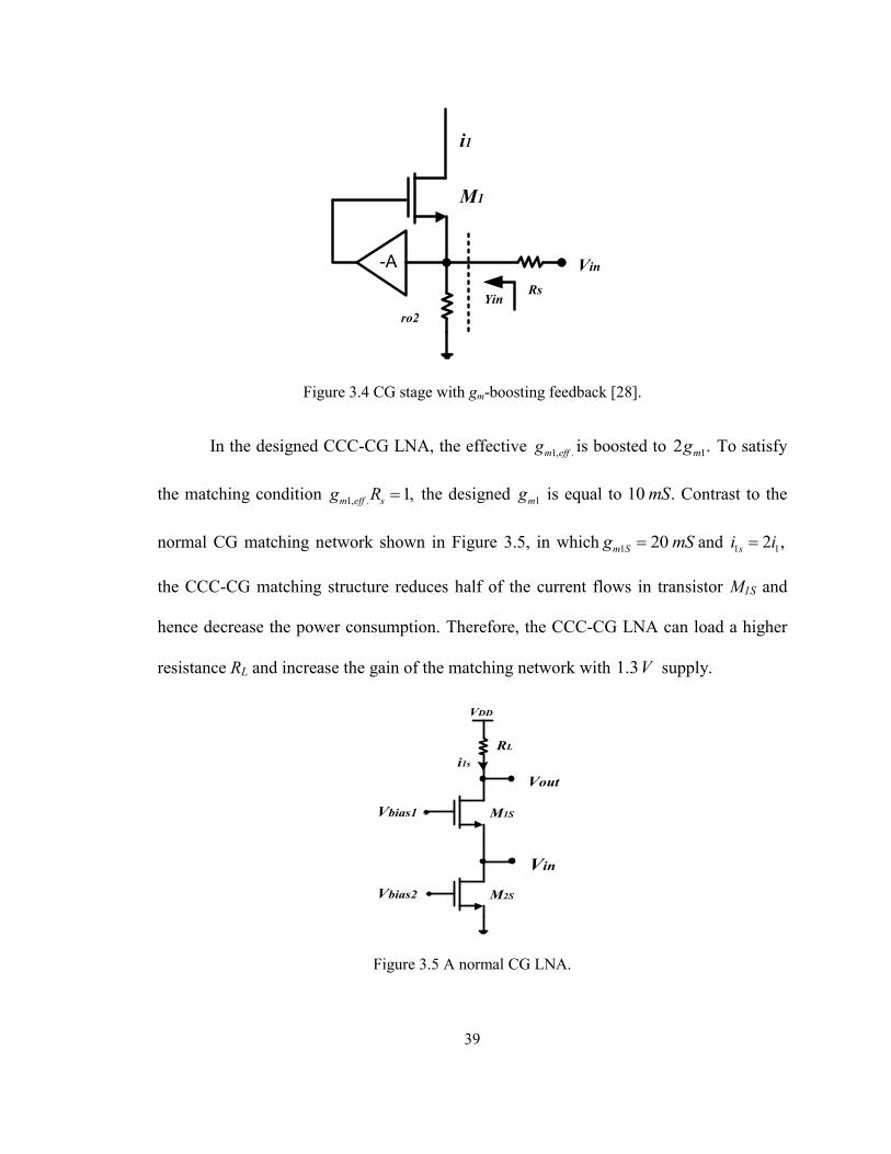
Figure 3.4 CG stage with gm-boosting feedback [28]. ................................................................... 39
Figure 3.5 A normal CG LNA. ...................................................................................................... 39
Figure 3.6 Traditional test setup for simulating a differential amplifier [30]. ............................... 41
Figure 3.7 Improved test setup of designed circuit [31]. ............................................................... 42
Figure 3.8 Simulated gain and S11from 0.7 to 2.5 GHz. ............................................................... 43
Figure 3.9 Simulated NF from 0.7 to 2.5 GHz. .............................................................................. 44
Figure 3.10 Simulated NF of the predistortion circuit from 0.7 to 2.5 GHz. ................................. 44
Figure 3.11 Third-order input intercept point of the CG LNA when f0=0.7 GHz. ......................... 45
Figure 3.12 Third-order input intercept point of the CCC-CG LNA when f0 =0.7 GHz. .............. 46
Figure 4.1 Block diagram of the system architecture. ................................................................... 49
Figure 4.2 Chip architecture. ......................................................................................................... 50
Figure 4.3 A basic current mirror. ................................................................................................. 52
Figure 4.4 Current bias network the CCC-CG matching network. ................................................ 54
Figure 4.5 An improved bias network of the CCC-CG stage. ....................................................... 55
Figure 4.6 Proposed active current amplification stage. ................................................................ 56
Figure 4.7 Laser diode power supply. ............................................................................................ 59
Figure 4.8 Harmonic balance simulation setup of the DFB-LD with predistortion circuit. .......... 60
Figure 4.9 Simulated spectra at the output of the DFB-LD, (a) without and (b) with predistortion
(matched) circuit. ................................................................................................................... 61
Figure 4.10 Simulated carrier and IMD3 of DFB-LD, with and without predistortion (matched)
circuit at 1600 MHz. ............................................................................................................... 62

xi
Figure 4.11 Simulated IMD3/C of DFB-LD, theoretical analysis, with and without predistortion
(matched) from 0.7 to 2.5 GHz. ............................................................................................. 64
Figure 4.12 Simulated IMD3/C with matched and unmatched predistortion circuit. .................... 65
Figure 4.13 Simulated phase difference between signal carrier and IMD3 with matched and
unmatched predistortion circuit. ............................................................................................ 65
Figure 4.14 Simulated output power of the predistortion circuit for different bias currents Ib2 and
Ib3. ........................................................................................................................................... 67

xii
List of Tables
Table 2.1 Transfer function coefficients of the 4th order polynomial curve fitting of the DFB-LD
transmission characteristics. ............................................................................................. 16
Table 2.2 Transfer function coefficients of the DFB-LD transmission characteristics.................. 17
Table 3.1 Simulated characteristics of CG LNA and CCC-CG LNA ............................................ 46
Table 4.1 Active current mirrors involved in Figure 4.6. .............................................................. 57
Table 4.2 Comparison of previously published predistortion design ............................................ 68

xiii
LIST OF ACRONYMS
ADC Analog-to-Digital Converter
BS Base Station
CAD Computer-aided Design
CCC-CG Capacitive Cross-coupled Common Gate
CG Common Gate
CMOS Complementary Metal-oxide-semiconductor
CMC Canadian Microelectronics Corporation
CS Common Source
CTB Composite Triple Beat Distortion
DC Direct Current
DFB-LD Distributed Feedback Laser Diode
DUT Device-Under-Test
EAM Electro-absorption Modulator
E/O Electrical-to-Optical
GSM Global System for Mobile Communication
HB Harmonic Balance
IC Integrated Circuit
IIP3 Input Referred Third-order Intercept Point
IMD Intermodulation distortion
IMD3 Third-order Intermodulation distortion
IP3 Third-order Intercept Point

xiv
LD Laser diode
LNA Low Noise Amplifier
MOS Metal-oxide-semiconductor
MOSFET Metal-oxide-semiconductor Field-effect Transistor
MZM Mach-Zehnder Modulator
NF Noise Figure
O/E Optical-to-Electrical
OSSB Optical Single Side Band
PCB Printed Circuit Board
PCCCS Polynomial Current Control Current Source
PD Photo Detector
PMOS P-channel MOSFET
PSS Periodic Steady-State
RAP Radio Access Point
RF Radio Frequency
RFIC Radio Frequency Integrated Circuit
RoF Radio-over-Fibre
SCM Subcarrier Modulation
SISO Single Input Single Output
S/N Signal-to-Noise
TE Transverse Electric
TM Transverse Magnetic
TSMC Taiwan Semiconductor Manufacturing Company

xv
UMTS Universal Mobile Telecommunication Systems
UWB Ultra-Wideband
VCO Voltage Controlled Oscillators
VLSI Very Large Scale Integration
WLAN Wireless Local-area Network

xvi
List of Principal Symbols
0I DC bias current
thI Threshold current of laser diode
thi i-th order
im Modulation index of thi carrier
i Phase of thi carrier
( )L t Output power of laser diode
0L Power at the DC bias current
opticalP Power received by power meter
outputI Current photodetected by PD
R Responsivity of a PD
.pdi RF signal current output of the predistortion circuit
ik Transfer function coefficients of DFB-LD
ia Transfer function coefficients of the predistortion circuit
inV Input RF signal provided to the predistortion circuit
mg Transconductance of MOSFET transistor
ig The thn order transconductance of MOSFET transistor
W Width of MOSFET transistor
L Length of MOSFET transistor
SSI Bias current of the differential pair

xvii
GSV Gate-source voltage
DSV Drain-source voltage
gsv Small signal gate-source voltage
ovV Overdrive voltage of MOSFET transistor
THV Threshold voltage of MOSFET transistor
OSV Offset voltage
ovV Thermal voltage
nF Noise figure of thn device
nG Power gain of thn device
CC Cross-coupled capacitor
gsC Parasitic capacitor
inY Input admittance
VA Voltage gain
LR Load resistance
SR Source resistance
n Channel mobility
oxC Capacitance per unit area
Channel-length modulation factor
mA Milli Ampere
mS Milli siemens

xviii
µm Micrometre
nm Nanometre
mV Milli Voltage
mW Milli Walt
1
CHAPTER 1 INTRODUCTION
1.1 Introduction
Mobile and wireless communications have experienced tremendous growth in the last
three decades. So far, three mobile standards have been successfully launched. Mobile
communications have evolved from the first-generation (1G) of analog systems in the
1980s to the second-generation (2G) of digital mobile systems in the 1990s. The Global
System for Mobile communication (GSM) standard which was developed in the 2G
systems provides national and international coverage. Current 2G and third-generation
(3G) systems are commonly used in mobile communication systems. The fourth-
generation (4G) of systems is under development and is expected to be available in the
near future. Apart from the mobile telephone communication, wireless networking is also
rapidly growing. The first Wireless Local-area Network (WLAN) developed in 1990 is
limited to low speed and narrow band operation. After that, various studies have been
devoted to broaden its operation bandwidth and boost the transmission data rate. During
the last 20 years, due to the fast evolution of wireless network services, broadband
communication and high-speed transmission are widely available for military and
commercial uses.
The rapid growth of mobile and wireless communications accelerates the
evolution of radio-over-fibre (RoF) technologies. To increase the bandwidth or, to
enhance the signal handling capability of a wireless access network, high carrier
frequencies or smaller cells (i.e. micro-cells and pico-cells) can be used. However, if
smaller cells are used, a larger number of Base Stations (BSs) or Radio Access Points
2
(RAPs) are needed to satisfy wide coverage and hence, increase the system cost.
Although a wired network offers broad bandwidth, it limits the overall convenience and
reduces the cost efficiency of systems. The RoF technology with low cost, high carrier
frequency and high bandwidth can have compatible properties of wired and wireless
network by arranging suitable locations of RAPs through the network along with mesh
routers.
In RoF systems, radio frequency (RF) signals are transmitted by using lasers and
optical fibre links [1]: the optical light generated from a laser source is modulated by an
RF signal and then transported over optical fibre links. This technology is widely used in
multi-service domains, like GSM, WLAN, and Universal Mobile Telecommunication
Systems (UMTS). Compared with other transmission media, optical fibre as the
backbone in RoF technology has unique properties, such as light weight, low attenuation
loss, small size, broad bandwidth and insensitivity to electromagnetic radiation. These
advantages make it as the optimal solution for transmitting RF signals efficiently in
wireless networks.
Power
Amplifier
Low Noise
Amplifier
Laser
Laser
Photo
Detector
Photo
Detector
Base StationCentral Site
Circulator Antenna
Rfin
Modulated
RfoutModulated
Figure 1.1 Radio-over-fibre system [1].
3
A typical RoF system is depicted in Figure 1.1. When a modulated signal (i.e.
GSM) is transmitted between the central site and base station, semiconductor lasers and
photo detectors (PDs) are employed as electrical-to-optical (E/O) converters and optical-
to-electrical (O/E) converters before and after the signal are distributed over optical fibre,
respectively. Generally, direct modulation of semiconductor lasers is the most cost
effective solution in comparison to other modulators, such as an Electro-absorption
Modulator (EAM) and a Mach-Zehnder modulator (MZM).
1.2 Motivation and Review of Technologies
Although these superior characteristics of optical fibre enable RoF technology as
an attractive approach in wireless communication, it is necessary to enhance the linearity
in optical links to improve the signal transmission quality. When multiple subcarrier
modulation (SCM) RF signals are introduced simultaneously in RoF links, undesired
harmonics and intermodulation distortion (IMD) products are generated due to the
nonlinearity of optical components, such as laser diodes (LDs), MZMs EAMs, and PDs.
These undesired products distort the received signals and degrade the overall system’s
performance. In RoF systems, it is required to keep the distortion below certain levels in
order to satisfy the quality of service provided to the users. Each user’s provided service
has required characteristics specified by the corresponding communication standard. For
example, the UMTS standard requires keeping the distortion 45dB lower than signal
carrier [2-3] for the down link.
In RoF systems, both modulation and photo-detection devices contribute to the
link distortion. Modulation devices usually are the main contributors to distortion

4
generation. Hence, it is critical to suppress the nonlinear distortion produced by
modulators. In general, even order distortion terms and harmonics fall far away from the
carrier frequency and can easily be filtered out, but third-order IMD (IMD3) terms are
close to carrier frequencies and are difficult to filter out. In order to minimize spectral
regrowth in the adjacent channels, the odd-order IMD products must be effectively
suppressed. Since distortion terms beyond 3rd
order are negligible, most linearization
work is focused on IMD3 cancellation.
Until now, many linearization technologies have been studied to improve the
linearity of optical components using optical or electrical techniques, such as mixed
polarization techniques [4], light injection techniques [5], feedforward linearization [6],
and analog predistortion techniques [2, 7-11].
Figure 1.2 Mixed polarization linearization of MZM for OSSB modulation [4].
A linearized Optical Single-sideband (OSSB) Mach-Zehnder modulator (MZM) is
given in [4]. The linearizer includes a linear polarizer with an angle of α with respect to
the z-axis, a dual-electrode z-cut LiNbO3 MZM, and a second linear polarizer with an
angle of β with respect to the z-axis, as shown in Figure 1.2. The anisotropic
characteristic of the z-cut LiNbO3 MZM enables the RF signal to be simultaneously

5
modulated in both orthogonal polarized states, Transverse Electric (TE) and Transverse
Magnetic (TM), by different modulation depth. When the optical signal exits the first
polarizer, z-(TM) axis will carry more IMD3 while the x-(TE) axis will carry less IMD3.
Followed by the MZM, the optical signal enters the second polarizer. Since the two
angles α and β are related to each other, therefore, the combined IMD3 from the two arms
of MZM can be suppressed by carefully selecting α and β of the two linear polarizes. This
mixed-polarization based linearization technique is mainly dependent on choosing α and
β, thus this linearization technique is limited to polarization dependent modulators.
However, this linearization method cannot be used to linearize LDs, which are known as
polarization independent components. On the other hand, high insertion loss is another
disadvantage of this technique. In the mixed polarization method, the signal carrier is
attenuated by more than 10 dB which decreases the transmitted signal significantly.
Laser (L1)
Laser (L2)Photodiode
(D1)
VGA (A2)VGA (A1)
Power
Splitter
(C1)
Input
Optical
Optical
Coupler (K1)
50/50 10/90
Optical
Coupler (K2)
Fiber Delay
-
+
180 Hybrid
Coupler (C2)
Electrical
delay
Electrical
delay
Photodiode
(D2)
Feedforward
output
Transmission
Fiber
Electrical
1
2
Figure 1.3 Diagram of a feedforward system [6].

6
A feedforward linearization technique is given in Figure 1.3. This system consists
of two loops: signal cancellation loop (the first loop) and distortion cancellation loop (the
second loop). In the first loop, the RF signal is split into two paths, where one modulates
the primary laser L1 and the other is the error-free reference path. Due to the nonlinearity
of laser L1, the signal at the output of the variable gain amplifier A1 contains carrier and
IMD products. Signal cancellation is achieved at the output of the 1800 hybrid coupler C2,
in which the output products of A1 are subtracted from the error-free reference path.
Ideally, only IMD3 distortion is left at the output of C2. The error signal at the output of
coupler C2 is shifted by 1800 and then injected into the second loop. The optical coupler
K2 combines the output signal of laser L2 and the signal transmitted from the optical fibre.
Distortion cancellation is realized at the output of the PD, since the PD functions as a
broadband in-phase microwave combiner. Furthermore, intensity laser noise can also be
reduced by this architecture. However, the feedforward technology requires accurate
amplitude and phase matching between the signal cancellation loop and the distortion
cancellation loop, which makes this technique difficult to achieve in practice, thus
limiting the amount of distortion reduction. In addition, the feedforward linearization
method requires extra LDs and PDs and hence, increases the cost and complexity of the
whole system.
Compared to the feedforward linearization method mentioned above,
predistortion techniques have become an attractive solution due to their lower cost, less
complexity and easy implementation. Predistortion circuits are designed which operate at
1350 MHz and 5800 MHz are reported in [8] and [9], respectively. In [7, 10], the
predistortion circuits are designed with CMOS 0.18 µm technology and operate in 1850 ~

7
2150 MHz and 50 ~ 500 MHz, respectively. In [2], they designed a predistortion
prototype using discrete diodes that can operate at 370 ~ 480 MHz, 820 ~ 960 MHz and
1710 ~ 1980 MHz. Two predistortion prototypes reported in [7] and [11] are reviewed in
detail.
Figure 1.4 Predistortion block diagram [7].
An adaptive CMOS predistortion linearizer is proposed in [7]. In this predistortion
prototype, shown in Figure 1.4, the input RF signal is firstly split into three paths: one
goes through the time delay path, the other two paths go through the nonlinearity
generation (second- and third-order distortion) circuits, and then these three paths are
combined after the power combiner. In this predistortion configuration, the power budget
and the complexity of the overall system are increased by additional phase-adjust and
gain-adjust blocks. To achieve a constant suppression over the bandwidth, it is required
to ensure that the correction tones produced by the predistortion circuit experience the
same delay and equal gain. Otherwise, linearity improvement will be hard to achieve.
8
Power
Splitter
Power
Combiner
DC Feed
RFvλ/4 transformer
inv λ/4 transformer
λ/4 transformer λ/4 transformer
DC Feed
Figure 1.5 Schematic diagram of anti-parallel diodes predistortion [11].
Recently, our group proposed a broadband predistortion of an EAM [11]. As
shown in Figure 1.5, the predistortion circuit consists of two power splitters/combiners,
anti-parallel diodes in two paths with push-pull bias and λ/4 impedance transformer
matching networks. In this circuit configuration, the input RF signal is equally converted
to two paths by a power splitter and transmitted through a pair of anti-parallel diodes.
Subsequently, the separated signals are recombined at the output of another power
combiner. The anti-parallel diode structure cancels the even order nonlinear products and
only the odd order distortions are left after the combiner. By tuning the bias current of the
diodes, the magnitude and phase of the carrier and IMD3 of this predistortion circuit can
be adjusted. Compared to current predistortion techniques, this design provides the
simplest approach and is suitable to linearize LDs. However, the λ/4 impedance
transformer networks occupy a large board area and introduce some signal losses.
1.3 Objective
The focus of this research work is on designing a simple and economical amplifier-based
tuneable RF integrated predistortion circuit to linearize distributed feedback laser diodes

9
(DFB-LDs) in the application of GSM, WLAN, and UMTS systems, which covers
0.7 ~ 2.5 .GHz The designed predistortion circuit will extend the output power of the
DFB-LD for which IMD3 is 45 dB lower than the carrier signal. This will enhance the
signal transmission capability of RoF systems significantly. In contrast to traditional
lossy predistortion, the proposed predistortion circuit predistorts and amplifies the signal
using a single path instead of the conventional two-path approach. The low noise and
high gain characteristics of the predistortion circuit make it able to process the signal
received from antenna without using additional amplifiers. The entire predistortion
system is single-input and single-output (SISO). This will significantly reduce the
complexity and cost of RoF systems.
1.4 Thesis Scope and Contributions
This thesis developed a gain boosting integrated circuit (IC) solution to suppress IMD3
distortion in optical fibre access communication systems. The predistortion circuit is
designed with TSMC90nm technology, which is supported by Canadian Microelectronics
Corporation (CMC). The proposed amplifier-based predistortion circuit has an equivalent
transconductance of 0.64 S over a bandwidth of 1.8 .GHz The simulated noise figure (NF)
of the entire predistortion circuit is 6.65 dB maximum.
The main challenges in this design are the broad operational bandwidth, which
covers 0.7 ~ 2.5 GHz and high modulation current generation, typically up to 25 .mA In
order to achieve the specified bandwidth, modulation current requirements and NF
minimization, 1.3V supply is selected (instead of the recommended1.2V ) with slight
increase in power dissipation.

10
The main contributions of this thesis are:
1. An amplifier-based tuneable RF predistortion for RoF systems was designed,
which covers the most significant frequency band of wireless access application
from 0.7 to 2.5 GHz.
2. The principle of the predistortion topology was analyzed. The transfer functions
of the predistortion linearizer were derived. The nonlinearity of a common-source
(CS) transistor, differential pairs and Gilbert cells were studied. A novel distortion
generation method based on existing linearization techniques was developed.
3. A capacitively cross-coupled (CCC-CG) low noise amplifier (LNA) was used for
broadband matching of the proposed triplet-core circuit to the50 characteristic
impedance of the RF chain. The noise performance of the matching network and
predistortion circuit were analyzed and simulated. The nonlinearity of the normal
common gate (CG) and the CCC-CG LNA were investigated.
4. Different types of current mirror were designed to bias and process the signal. The
current injection technique was used to improve the conversion gain and reduce
system power dissipation. The entire predistortion circuit supplies both DC
current and modulation signal to the DFB-LD.
1.5 Thesis Outline
The rest of the thesis is organized as follows:
The principle of predistortion linearization is discussed in Chapter 2. The
nonlinear transfer function of a DFB-LD is measured experimentally and modeled with
the 4th
order polynomial equation. To linearize the DFB-LD, the transfer function of

11
predistortion circuit is derived. The nonlinear characteristics of a single transistor,
differential pairs and Gilbert cells are discussed. After a review of the Multi-tanh
principle of Gilbert cells, the triplet-core circuit is proposed and its nonlinear
characteristic is analyzed and computed using Cadence Virtuoso Hspice/Spectre circuit
simulators.
Chapter 3 describes the matching network design of the proposed triplet-core
circuit. A gm-boosting CCC-CG topology is analyzed. A differential test bench is studied
and applied to simulate the matching behavior and noise performance of the designed
LNA. The nonlinearity of the matching network is simulated.
Chapter 4 begins with the architecture of the whole system design. From the
system point of view, a 1800 coupler is used to convert the single input to differential
inputs in the printed circuit board (PCB) design process. The matching network has a
fully differential configuration while the distortion generator converts the differential
input to a single ended output. Therefore, the matching stage and distortion generator can
be connected to one another. This chapter explains the detailed design work. Various
current mirrors are described, such as basic current mirrors, cascode current mirrors and
active current mirrors. The current injection technique is also described. The designed IC
supplies both bias current and modulation current to directly drive the DFB-LD. Finally,
simulation results are presented and discussed.
Chapter 5 gives concluding remarks, the progress that has been accomplished and
suggests some future work.

12
CHAPTER 2 THE PRINCIPLE OF PREDISTORTION
2.1 Introduction to Distributed Feedback Laser Diode
Nowadays, semiconductor LDs are one of the most common electro-optic devices used in
RoF systems due to their advantages, such as small size, cost-effectiveness, simplicity
and ease of monolithic integration with other E/O components. Like other modulators,
LDs are the main nonlinear contributors in RoF systems. The nonlinear characteristics of
an LD introduce many harmonics and IMD products if SCM is used, and these nonlinear
products degrade the performance and sensitivity of RoF systems. Therefore, it is highly
desirable to develop linearization techniques to compensate the nonlinear distortion.
A DFB-LD is a semiconductor LD, in which a diffraction grating is etched close
to the p-n junction of the diode in order to achieve the selectivity of lasing wavelength.
The optical grating acts like an optical filter, where all these small reflections are added
in phase. Ideally, only one wavelength is selected by the optical grating and fed back to
the gain region and lases. Figure 2.1 shows one possible way to incorporate a grating
within a diode laser cavity. In a DFB-LD, the intensity of the laser output will be changed
directly by the modulation signal. Also, the optical output power of the LD and its lasing
frequencies are fluctuating with the modulation signal. Therefore, DFB-LD is a
frequency dependant direct modulator.

13
n
p
Active
Layer
PL,O
Bottom
ContactAnti-reflection
Mirror
Light
Beam Substrat
Top
Contact
Figure 2.1 Diagram of a DFB-LD with Bragg grating on the top [12].
2.2 Mathematical Analysis of Predistortion
To linearize the DFB-LD, it is necessary to study its nonlinear characteristics. There are
two approaches in evaluating the nonlinear distortion of a DFB-LD in multichannel
transmission: one is based on dynamic modeling of the rate equations [13], while the
other is based on static modeling of the light-current characteristics (typically, L-I curve)
[14]. Compared with rate-equations-based modeling, L-I curve modeling is an easier
approach to evaluate the nonlinear characteristics of a DFB-LD. In this work, the
nonlinearity of the DFB-LD is studied with its static L-I curve. The modulation current
provided to the laser is described in [14] as
0 0 1( ) ( ) cos(2 )
N
th i i iiI t I I I m f t
(2.2.1)
I0 is the DC bias current, Ith is the threshold current of the laser, mi is the modulation
index of the ith
carrier, and φi is the phase of ith
carrier. In response to the modulation, the
light output L (t) is given by

14
0 01
/( ) [ ( ) ]
!
n nN n
i
d L dIL t L I t I
n (2.2.2)
where L0 is the power at the DC bias current.
2.2.1 Modeling of Nonlinear Transmission Characteristics of a DFB-LD
in RoF Systems
To accurately analyze the nonlinearity of the DFB-LD, we first perform the experiment to
measure its nonlinear transmission characteristics. The experimental setup consists of a
current source, a DFB-LD and an optical power meter. During the experiment, the bias
current supplied to the DFB-LD is adjusted from 1 to 125 mA, with a step of 1 mA and
the optical power is measured at each step. The DFB-LD starts lasing when operating
beyond its threshold current. The threshold current of the tested DFB-LD is 8 mA . The
measured L-I curve on a linear scale is shown in Figure 2.2.
0
0.4
0.8
1.2
1.6
0 20 40 60 80 100 120
Op
tica
l o
utp
ut
(mW
)
Bias current (mA)
Figure 2.2 Measured nonlinear characteristics of a DFB-LD.

15
Poptical is the power received by the power meter. Converting Poptical to the current
photodetected by PD, Ioutput, we have
output opticalI P R (2.2.1.1)
Where R is the responsivity of the PD. Typically, R is 0.6, which refers to the optical to
electrical conversion efficiency of the PD.
To investigate the nonlinearity of the DFB-LD, we fit the I-I curve (bias current
of DFB-LD versus current detected by PD) by a polynomial using curve fitting functions
in Kaleidagraph. The model is built by writing the nonlinear equation to a Polynomial
Current Control Current Source (PCCCS), which is available in the Analog Library of
Cadence. The proposed predistortion circuit is designed and simulated based on the
PCCCS model.
The considered modulation and bias current of the DFB-LD are 25 mA and
35 ,mA respectively. Therefore, the photodetected current Ioutput in terms of bias current is
obtained by polynomial curve fitting within the operation range, i.e. 10 ~ 70 mA. Some
bias currents that are below or close to threshold are ignored. The fitted curve with bias
current of the DFB-LD is plotted in Figure 2.3. A 4th
order polynomial curve fitting is
well matched with the measured nonlinear transmission characteristics. The nonlinear
characteristic of the DFB-LD is described in equation (2.2.1.2). Table 2.1 gives the value
of transfer function coefficients.
2 3 4
0 1 2 3 4( ) ( )outputI I f I M M I M I M I M I (2.2.1.2)
Where ( 0,1,2,...,4)iM i are the transfer function coefficients of the I-I curve.
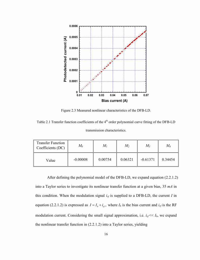
16
0
0.0001
0.0002
0.0003
0.0004
0.0005
0.0006
0.01 0.02 0.03 0.04 0.05 0.06 0.07
Ph
oto
de
tec
ted
cu
rre
nt
(A)
Bias current (A)
Figure 2.3 Measured nonlinear characteristics of the DFB-LD.
Table 2.1 Transfer function coefficients of the 4th order polynomial curve fitting of the DFB-LD
transmission characteristics.
Transfer Function
Coefficients (DC)
M0 M1 M2 M3 M4
Value
-0.00008 0.00754 0.06321 -0.61371 0.34454
After defining the polynomial model of the DFB-LD, we expand equation (2.2.1.2)
into a Taylor series to investigate its nonlinear transfer function at a given bias, 35 mA in
this condition. When the modulation signal irf is supplied to a DFB-LD, the current I in
equation (2.2.1.2) is expressed as ,b rfI I i where Ib is the bias current and irf is the RF
modulation current. Considering the small signal approximation, i.e. irf << Ib, we expand
the nonlinear transfer function in (2.2.1.2) into a Taylor series, yielding

17
2 3
0 1 2 3( ) ( ) ..... ...n
rf rf rf rf n rfoutputI I f i k k i k i k i k i (2.2.1.3)
Where ( 1,2,3,..., ,...)ik i n are the Taylor series coefficients
1
( )
1!
bf Ik
2
( ),
2!
bf Ik
( )..., ,...
!
n
bn
f Ik
n The transfer function coefficients in terms of irf are shown in Table 2.2.
Table 2.2 Transfer function coefficients of the DFB-LD transmission characteristics.
Transfer Function
Coefficients (AC)
k0 k1 k2 k3 k4
Value
0.0002 0.0098 0.0013 -0.5655 0.3445
2.2.2 Mathematical Analysis of Predistortion
The block diagram of the predistortion circuit followed with a DFB-LD is depicted in
Figure 2.4.
Predistortion3
. 1 3pd in ini a av v
Distributed Feedback
Laser Diode Model3
1 . 3 .out pd pdi k ki i
inv .pdi outi
Figure 2.4 Block diagram of predistortion circuit and DFB-LD.
The proposed predistortion circuit is transconductance based and the DFB-LD is
modeled by a PCCCS and hence, the output of predistortion circuit and input of DFB-LD
are expressed in current mode. In this work, we are only concerned about the IMD3
18
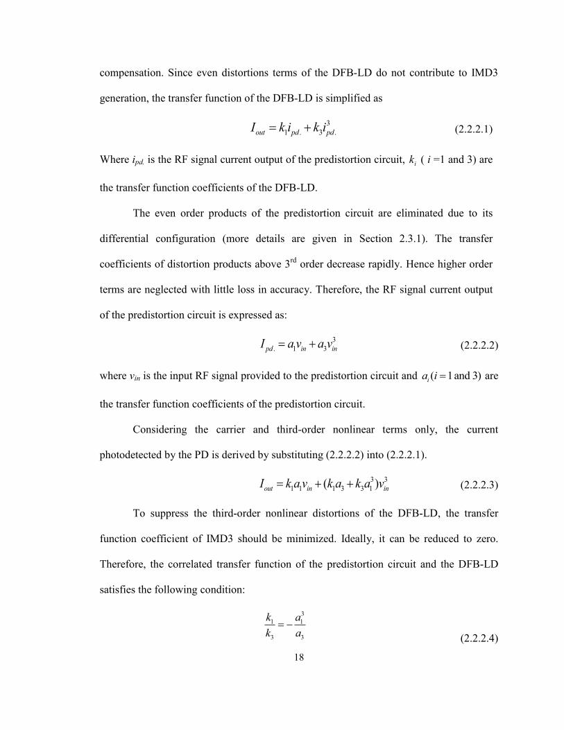
compensation. Since even distortions terms of the DFB-LD do not contribute to IMD3
generation, the transfer function of the DFB-LD is simplified as
3
1 . 3 .out pd pdI k i k i (2.2.2.1)
Where ipd. is the RF signal current output of the predistortion circuit, ik ( i =1 and 3) are
the transfer function coefficients of the DFB-LD.
The even order products of the predistortion circuit are eliminated due to its
differential configuration (more details are given in Section 2.3.1). The transfer
coefficients of distortion products above 3rd
order decrease rapidly. Hence higher order
terms are neglected with little loss in accuracy. Therefore, the RF signal current output
of the predistortion circuit is expressed as:
3
. 1 3pd in inI a v a v (2.2.2.2)
where vin is the input RF signal provided to the predistortion circuit and ( 1and 3)ia i are
the transfer function coefficients of the predistortion circuit.
Considering the carrier and third-order nonlinear terms only, the current
photodetected by the PD is derived by substituting (2.2.2.2) into (2.2.2.1).
3 3
1 1 1 3 3 1( )out in inI k a v k a k a v (2.2.2.3)
To suppress the third-order nonlinear distortions of the DFB-LD, the transfer
function coefficient of IMD3 should be minimized. Ideally, it can be reduced to zero.
Therefore, the correlated transfer function of the predistortion circuit and the DFB-LD
satisfies the following condition:
3
1 1
3 3
k a
k a
(2.2.2.4)

19
Normally, in nonlinear devices, such as optical modulators and amplifiers, carrier
and IMD3 terms are out of phase, which is known as a gain compression characteristic.
Consequently, to achieve IMD3 compensation, the carrier and IMD3 of the predistortion
circuit should be in phase, which is known as a gain expansive characteristic. The
proposed predistortion is voltage input and current output. With the transfer function
coefficients k1 and k3 given in Table 2.2 and equation (2.2.2.4), the normalized
transconductance gm curve of the predistortion circuit in terms of input voltage is plotted
in Figure 2.5.
1
1.1
1.2
1.3
1.4
1.5
1.6
-0.1 -0.05 0 0.05 0.1
desired gm
No
rma
lize
d g
m
Vin
(V)
Figure 2.5 Desired gm curve of the predistortion circuit.
Assuming the photodetected output current of the DFB-LD is fed to a 50 load,
the nonlinear characteristics of the DFB-LD without predistortion and theoretical analysis
of the compensated DFB-LD with predistortion circuit are plotted in Figure 2.6. As
shown in Figure 2.6, the free-running DFB-LD cannot fulfill the requirement of keeping
the IMD3 45 dB lower than the signal carrier when the processed signal is greater than
11mA (corresponding to 35.4 dBm output RF power in Figure 2.6). The third-order

20
nonlinearity is suppressed as can be seen from the slope of 5 in IMD3 when using the
predistortion circuit. From a system point of view, the amplifier-based predistortion
circuit enhanced the power transmission capability and increase the signal-to-noise (S/N)
ratio of RoF systems. Therefore, the power boosting predistortion circuit minimized the
system cost and power consumption of the entire system. Ideally, with the predistortion
circuit, the DFB-LD can handle 21mA signal current (corresponding to 30.3 dBm
output RF power in Figure 2.6) within the system linearity requirement.
-120
-100
-80
-60
-40
-20
-40 -38 -36 -34 -32 -30
Carrier
without predistortion
required
theoretical compensation
Carr
ier
an
d I
MD
3 (
dB
m)
Output RF power (dBm)
3
5
Figure 2.6 Nonlinear characteristic of DFB-LD with theoretical predistortion cancellation.
2.3 Triplet-Core Circuit
To build a CMOS predistortion circuit, nonlinear characteristics of three different circuit
configurations are studied: a single CS transistor, a differential pair and Gilbert cells.
Based on the Multi-tanh linearization technique, a novel distortion generation method is
developed.

21
2.3.1 Nonlinear Transconductance of a Single Transistor and
Differential Circuits
Consider a single CS MOSFET biased in saturation. The small-signal output current
depends on the gate-source (VGS) and drain-source voltages (VDS), but the dependence on
VDS for a transistor in saturation can be ignored here with little loss in accuracy [15].
Expanding its output drain current into a one-dimensional Taylor series in terms of the
small-signal gate-source voltage (vgs) around the bias point, we get
2 3
1 2 3( ) ...d gs gs gs gsi v g v g v g v (2.3.1.1)
where g1 is the small-signal transconductance, g2, g3, … are the higher-order coefficients
which define the intensity of the corresponding nonlinearity. Of all these coefficients, g3
is particularly important because it controls the third-order nonlinear distortion, hence
determining the input referred Third-order Intercept Point (IIP3) [16-17]. The first three
coefficients gi (i = 1, 2, and 3) can be found by taking the ith
derivative of equation
(2.3.1.1) in terms of vgs
2 3
1 2 32 3
1 1
2 6
D D D
GS GS GS
I I Ig g g
V V V
(2.3.1.2)
In the simulation, by sweeping VGS of a CS NMOSFET with a dimension of W/L
(10 µm/100 nm) and a fixed VDS, the first three derivatives of drain current in terms of
VGS are plotted in Figure 2.7. As depicted in Figure 2.7, when VGS transitions from the
weak to moderate inversion region or the strong inversion region, the dependence of g3
on VGS is such that g3 changes from positive to negative (contrasting to g1). Figure 2.8
depicts the corresponding absolute value of 2 1/g g and 3 1/g g on a log scale. As shown

22
in Figure 2.8, the nonlinearity of a transistor varies with the overdrive voltage. In the
strong inversion region, transistor always has higher linear transconductance and lower
second- /third-order distortion coefficients.
-0.05
0
0.05
0 0.2 0.4 0.6 0.8 1
g1
g2
g3
g1
(A
/V), g
2 (
A/V
2) an
d g
3(A
/V3)
VGS
(V)
Figure 2.7 Simulated DC characteristics of a W/L (10 µm/100 nm) NMOSFET.
-3
-2
-1
0
1
2
0 0.2 0.4 0.6 0.8 1
abs(g2/g
1)
abs(g3/g
1)
ab
s(g
2/g
1)
an
d a
bs(g
3/g
1)
(dB
)
VGS
(V)
Figure 2.8 Simulated g2/g1 and g3/g1 ratio of a W/L (10 µm/100 nm) NMOSFET.

23
Some efficient linearization methods based on the DC characteristics of a CS
transistor are described in [15-17]. The nonlinearity of a single CS transistor can be
improved by using multiple gate transistors: the main transistor operates in the saturation
region while an auxiliary transistor with different size operates in the weak inversion
region which nulls the negative 3rd
order derivative g3 of the main transistor. This is
known as derivative superposition method [16]. However, with this linearization
topology, it is hard to build a widely tuneable and high gain predistortion circuit due to its
low signal handling capability and high tuning sensitivity in the weak inversion region.
Numerous linearization techniques have been developed with differential pairs.
Compared to a single CS transistor, it demonstrates an “odd-symmetric” input/output
characteristic and correspondingly exhibits much less distortion [18-19]. A schematic
diagram of a basic differential pair is shown in Figure 2.9.
Iss
I1 I2
Vin
M1 M2
Figure 2.9 Basic differential pair.
Assuming transistors M1 and M2 are identical long channel MOSFET, biased in
the saturation or strong inversion region. The output current is developed as:
2
0 1 2 2 12
SSSS in in in
SS
IKI I I I KV V V
I K (2.3.1.3)

24
where 1
( )2
n ox
WK c
L and ISS is the bias current of the differential pair.
Expanding (2.3.1.3) into a Maclaurin series, yields
3/23
0
3
12 ...
2 2
12 ... 2
4
SSSS in in in
SS
ov in in in ov
ov
IKI I KV V V
KI
KKV V V V V
V
(2.3.1.4)
We have
ov GS THV V V (2.3.1.5)
Where Vov is the overdrive voltage and VTH is the threshold voltage of M1 and M2.
Equation (2.3.1.4) indicates that the nonlinearity decreases with increasing Vov. With a
fixed transistor size of M1 and M2, increasing Vov, the first-order transfer function
coefficient increases while the third-order’s decreases. Consequently, the amplitude of
signal carrier is increased and third-order distortion terms are reduced and hence, the
nonlinearity of the differential pair is reduced. However, increasing Vov leads to large
power dissipation. Thus, it is necessary to tradeoff transistor size and power dissipation.
The DC characteristic of the differential pair is simulated in Hspice. By sweeping
Vin, the desired output current I1 and I2 can be obtained from the differential pair circuit.
As illustrated in Figure 2.10, the output currents I1 and I2 are odd functions of Vin. 1 2I I
falls to zero when Vin = 0. Beyond 2 ,in ovV V one transistor carries the entire ISS while
the other is turned off. The equivalent transconductance of M1 in the differential pair is
plotted in Figure 2.11.

25
-1.4
-1.2
-1
-0.8
-0.6
-0.4
-0.2
0
-200 -150 -100 -50 0 50 100 150 200
I1
I2
Cu
rren
t o
utp
ut
(mA
)
Vin
(mV)
Figure 2.10 Voltage-current (V-I) characteristic of the differential pair.
0
0.5
1
1.5
2
2.5
3
-300 -200 -100 0 100 200 300
gm
gm
(m
S)
Vin
(mV)
Figure 2.11 gm of transistor M1.
The gm of M1 in terms of Vin is developed as:
2 2
2
2 2
2
2[1 ] 2 [1 ]
1 12
in inSS ov
SS ov
m
in in
SS ov
KV VI K KV
I V
KV V
I V
g
(2.3.1.6)
As shown in Figure 2.11, the transconductance gm is a symmetric function of Vin.

26
The shape of the transconductance gm curve in Figure 2.11, along with its relationship
with the overdrive voltage ovV can be used to evaluate the nonlinearity of differential pairs.
Generally, with fixed transistor sizes, higher ISS contributes to a higher Vov and hence
expands the gm curve. High linearity in differential pairs is obtained at Vin = 0, but
degrades with large input signal.
With MOSFETs scaling down below 100 nm, the square-law model is no longer
accurate [20]. However, the basic observations made in this section about the large-signal
operation of the MOS differential pair are still valid. In particular, the differential pair
still gives rise to a compressive nonlinearity.
2.3.2 Introduction of Gilbert Cell and the Multi-tanh Principle
The Gilbert cell was first described by Barrie Gilbert in 1968. Gilbert cell is built by
connecting the input and output of differential pairs in parallel [21]. The Multi-tanh
principle of Gilbert cell is named based on its topological and mathematical aspects. If
( 2)n n differential pairs are connected in parallel, their individual nonlinear
transconductance can be expanded along the input-voltage axis by applying input offset
voltages. Offset voltage can also be supplied by selecting the emitter area ratio of
differential pairs. The Multi-tanh configuration enhances the large signal handling
capability of individual differential pairs. If the overall transconductance is extended to a
wider region, it can provide a low-distortion scheme. Such a cell gives a highly linear
transconductance, hence it is widely used to build linear amplifiers, mixer, voltage
controlled oscillators (VCOs), tuneable filters, or other active elements.

27
The doublet, in which two differential pairs are connected in parallel, is the
simplest form of a Gilbert cell. To illustrate the Multi-tanh principle, the doublet is
discussed as an example. A bipolar transistor based doublet is shown in Figure 2.12.
Vin
Iout
IT
Q1
Ae e
e
IT
Q2
Q3
Q4
Ae
Figure 2.12 Basic Multi-tanh doublet [21].
In Figure 2.12, differential pairs Q1-Q2 and Q3-Q4, are biased with equal tail
current IT. The offset voltages are provided by making the emitters’ area ratio of Q1 and
Q4 “A” times of Q2 and Q3. The emitter area ratio “A” shifts the peak of each gm by an
equivalent offset voltage Vos. The relationship between A and Vos satisfies
lnos TV V A (2.3.2.1)
where VT is the thermal voltage.
The overall gm is much more linear compared with each individual
transconductance, as illustrated in Figure 2.13. In the doublet circuit, the original gm is
reduced by a factor of 24 / (1 )A A [21]. In order to reach the same conversion gain, ISS
and the diffusion area should be multiplied by 2(1 ) / 4A A . From this point of view, the

28
linearity of the Gilbert cell is achieved at the expense of increasing the system power
dissipation and using large transistors.
0
1
2
3
4
-200 -100 0 100 200
gm
(m
S)
Vin (mV)
sum
gm1 gm2
Figure 2.13 Dual gm components for the doublet.
2.3.3 Proposed Triplet-Core Circuit
The Multi-tanh principle can also be applied to MOSFETs, since MOS transistors
operating in the sub-threshold and saturation region behave almost exactly like bipolar
transistors. The concept that works in strong inversion: the width ratio of transistors gives
an input offset voltage which shifts the peak of the gm curve away from 0.inV In the
doublet circuit, if the peak of each individual gm is shifted further with higher offset
voltage, a valley appears at the center of the gm curve. Therefore, the gm curve of the
doublet circuit has the similar shape with the desired transconductance of predistortion
circuit, as depicted in Figure 2.14. The gm curve of MOSFET based doublet and the
desired gm curve are shown in Figure 2.14. The doublet circuit has a simple architecture
29
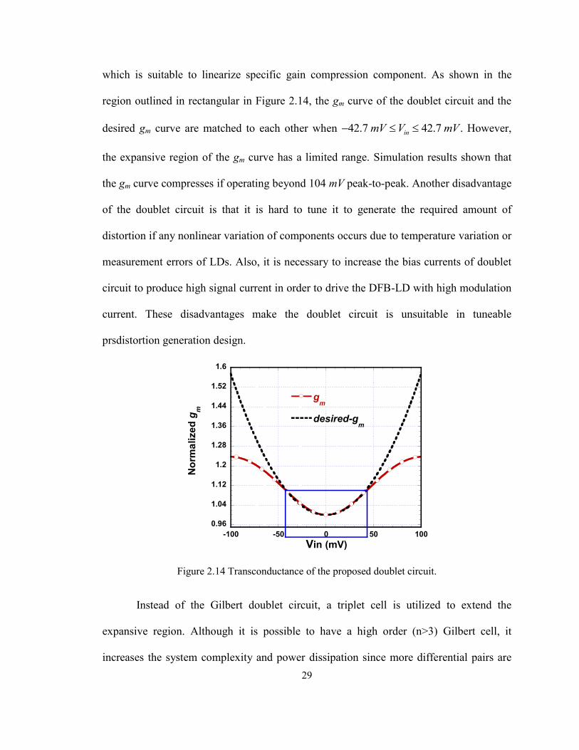
which is suitable to linearize specific gain compression component. As shown in the
region outlined in rectangular in Figure 2.14, the gm curve of the doublet circuit and the
desired gm curve are matched to each other when 42.7 42.7 .inmV V mV However,
the expansive region of the gm curve has a limited range. Simulation results shown that
the gm curve compresses if operating beyond 104 mV peak-to-peak. Another disadvantage
of the doublet circuit is that it is hard to tune it to generate the required amount of
distortion if any nonlinear variation of components occurs due to temperature variation or
measurement errors of LDs. Also, it is necessary to increase the bias currents of doublet
circuit to produce high signal current in order to drive the DFB-LD with high modulation
current. These disadvantages make the doublet circuit is unsuitable in tuneable
prsdistortion generation design.
0.96
1.04
1.12
1.2
1.28
1.36
1.44
1.52
1.6
-100 -50 0 50 100
gm
desired-gm
No
rma
lize
d g
m
Vin (mV)
Figure 2.14 Transconductance of the proposed doublet circuit.
Instead of the Gilbert doublet circuit, a triplet cell is utilized to extend the
expansive region. Although it is possible to have a high order (n>3) Gilbert cell, it
increases the system complexity and power dissipation since more differential pairs are

30
involved. The triplet cell is designed to generate the desired gm to compensate the
nonlinearity of the DFB-LD rather than to make a linear gm curve. There are two ways to
implement the triplet cell. One is to shift the two peaks of gm further and add another
differential pair, which has a smaller transconductance. The other approach is to make a
doublet cell with a wider linear region, which can be obtained with higher overdrive
voltage. By subtracting the extra gm curve of the third additional differential pair, we
obtained the desired curve. Comparing these two approaches, the second option provides
wider expansive region and hence, is used to build the proposed triplet-core circuit. The
triplet-core circuit and the corresponding gm curves are shown in Figure 2.15 and Figure
2.16.
M1A
Vin
Iout
I1=IT I2=KIT
M2A M3A
M1B M2B M3B
I3=IT
A
A
Figure 2.15 Schematic diagram of the proposed triplet-core circuit.

31
-5
0
5
10
15
-400 -300 -200 -100 0 100 200 300 400
gm
(m
S)
Vin (mV)
gm gm
M1A-M1B M2A-M2B
gm
M3A-M3B
sum
Figure 2.16 gm curves of proposed triplet-core circuit.
As explained in Section 2.3.1, the nonlinearity of the differential pair depends on
the tail current, given by I1, I2 and I3 of the triplet-core circuit. Consequently, tuning I1, I2
and I3 shifts gm the curves and hence varies the nonlinearity of the triplet-core circuit. In
this work, the offset voltage of the outer differential pairs are provided with a transistor
width ratio “A”, “A” is equal to 8 and K is equal to 0.33 in this design. No offset voltage
is applied to the inner pair. The current subtraction is achieved if the output of the inner
differential pair (M2A/M2B) is cross-coupled with the outer pairs (M1A/M1B and M3A/M3B).
Obviously, this triplet-core circuit has a fully differential configuration. Since the outer
differential pairs have a symmetrical structure, I1 and I3 can be controlled by one current
mirror. Therefore, two current sources Ib2 and Ib3 are used to adjust tail currents: Ib2
controls I1 and I3 while Ib3 controls I2. The detailed schematic diagram of the triplet-core
circuit is given in Figure 4.2.

32
The nonlinearity of the triplet-core is tuneable. As depicted in Figure 2.17 and
Figure 2.18, when the tail currents of the outer pairs I1 and I3 are increased from 2.4 mA
to 3.0 ,mA the nonlinearity of triplet-core is decreased; while tuning the tail current of
inner pair I2 from 0.8 mA to 2.0 ,mA the nonlinearity at higher level, beyond 100 mV
peak-to-peak, is reduced. DC sweeps also indicate how to tune the nonlinearity of the
triplet-core circuit to get the desired gm curve: tuning I1 and I3 to fit the overall gm with
low signal input and tuning I2 to fit the overall gm with high signal input.
1
1.1
1.2
1.3
1.4
1.5
1.6
1.7
-100 -50 0 50 100
2.4 mA
2.7 mA
3.0 mA
desired-gm
No
rmalized
gm
Vin (mV)
Figure 2.17 Overall gm curves by tuning I1 and I3.
33
1
1.1
1.2
1.3
1.4
1.5
1.6
-100 -50 0 50 100
0.8 mA
1.4 mA
2 mA
desired-gm
No
rma
lize
d g
m
Vin (mV)
Figure 2.18 Overall gm curves by tuning I2.
2.4 Conclusion
In this chapter, we studied and measured the nonlinear transfer characteristic of the DFB-
LD. The nonlinear polynomial model of the DFB-LD is defined with PCCCS in Cadence
and is suitable for predistortion circuit design and simulation. Based on the desired
transcondutance of the predistorter derived from mathematical analysis, various distortion
characteristics of a single CS transistor, differential pairs and Gilbert cells are reviewed.
The nonlinearity of the proposed triplet-core circuit can be tuned by adjusting bias
currents I1, I2 and I3. The highly tuneability enhanced the linearization and nonlinearity
variation handling capabilities of the proposed predistortion circuit.

34
CHAPTER 3 INPUT IMPEDANCE MATCHING NETWORK
DESIGN OF THE PROPOSED TRIPLET-CORE CIRCUIT
3.1 Introduction
Impedance matching is an essential part of RF circuit design for maximum power
transmission and is therefore discussed in detail in numerous sources [22-25]. As we
know, the Gilbert cell configuration is usually noisy because of the current subtraction of
differential pairs [24]. Input matching condition and NF are figures of merit to measure
the matching network. Since impedance matching and NF are correlated [25], it is
necessary to come up with a solution to match the triplet-core circuit and reduce its affect
on the NF of systems.
When n blocks are cascaded, the NF of the entire system is given by [26]
321
1 1 2
11...
FFF F
G G G
(3.1.1)
Where ( 1,2,3,...)nF n is the NF for the nth
block and ( 1,2,3,...)nG n is the linear
power gain of the nth
block.
This is known as the Friis formula and typical results show that the most critical
stage is usually the first stage. Hence, the NF of the first stage usually dominates the
sensitivity of the entire system. Consequently, it is promising to design an impedance
matching network and diminish the NF of the triplet-core circuit by cascading an LNA
which provides enough gain and low NF in front.
35
Many LNAs presented in other works (i.e. [27-28]) have achieved a good
matching and high gain. In this work, a gm-boosting CCC-CG topology [28-29] is
selected to match to triplet-core circuit to 50 . Noise performance and the gain of the
proposed CCC-CG matching network are analyzed. S11 and NF are performed with S-
parameter simulation using the Spectre simulator in Cadence. The capacitively cross-
coupled gm-boosting technology is a power reduction approach, which also indicates that
the same signal current will be modulated on the reduced DC current. The increased
signal density would degrade the nonlinearity of system. Based on this consideration, the
nonlinearity of CG with and without capacitively cross-coupled structures are simulated.
3.2 Capacitively Cross-coupled Common Gate LNA
The basic CS LNA topology is widely used because it provides good noise performance
and high gain. In a CS configuration, source degeneration inductors are usually applied to
the source of the active transistors in order to make a 50 Ω input matching network.
However, using this approach it is hard to meet the broadband matching and gain flatness
requirements. A three-section band-pass Chebyshev filter [22] or a two-section LC ladder
[23] can achieve broadband matching and good noise performance. However, extra
elements involved in the matching network increase the area and the complexity of the
chip. Additionally, a CS LNA consumes high power. These disadvantages make the CS
LNA a non-optimal choice in low power LNA design.
In contrast to CS LNA, CG LNA is a simpler approach due to its superior
broadband input matching, linearity and low power consumption advantages. However,

36
the shortcoming of a CG LNA is that it presents a relatively high NF. A basic CG LNA is
shown in Figure 3.1.
M
RsVin
Ls
VDD
Lload
Vout
Vbias
Figure 3.1 Basic CG LNA.
The dominant noise sources of the basic CG LNA are the noise current ins of the
source resistance ,sR and the drain current noise source ind as shown in Figure 3.2, while
the NF contributed by the gate noise of transistor M is usually negligible. The NF of the
CG LNA is
2 2
2 2
1( )1
1
( )1
nd
m S
m Sns
m S
ig R
g Ri
g R
F
(3.2.1)
With 2
04nd di kT g f and 2 14 ,ns Si kTR f where 0dg is the zero bias drain conductance
of transistor M. SR is the source resistance. With an input matching condition of
1,m Sg R equation (3.2.1) reduces to

37
20
1
0
2
4 11 ( )
4
1 1
d
S m S
d
m S
kT g f
kTR f g R
g
g R
F
(3.2.2)
Where γ is the channel thermal noise coefficient (γ is typically 2/3 for long channel
transistors and 2 for short channel transistors) and 0/ .m dg g It is reported in [27] that
the minimum NF of a CG-LNA is limited to3 .dB
M
Rs
ino
ins
ind
Figure 3.2 Dominant noise sources in the basic CG LNA [29].
To improve the noise performance of a CG LNA, a capacitively cross-coupled gm-
boosting scheme is introduced in [27-29]. The presented CCC-CG LNA in [28] is
inductively degenerated which occupies a large chip area and increases the cost of the
chip. In this design work, current source transistors are used to achieve broadband
matching with slightly increased NF. The designed CCC-CG LNA which is fully
differential is shown in Figure 3.3.

38
M3 M1
Vdd
Cc CcVinn Vinp
M4 M2
Vbias1
RL RL
Von Vop
Vdd
Vbias2
i1i2
Figure 3.3 Proposed fully differential CCC-CG LNA.
The inverting amplification value “A” in half circuit analysis in Figure 3.4 is
approximately equal to the capacitor voltage division ratio
1/ 1
1/ 1/ 1 /
gs
c gs gs c
AC
C C C C
(3.2.3)
Where CC is the cross-coupled capacitor and gsC is the parasitic capacitance of transistor
M1 and M2. Thus, the effective transconductance is expressed as
1, . 1
2gs c
m ef f m
gs c
C Cg g
C C
(3.2.4)
Usually, CC >>Cgs,yielding 1A and
1, . 1 1(1 ) 2m eff m mg A g g (3.2.5)
The overall input admittance is
1, . 2 11/in m eff o gsY g r sC (3.2.6)
The voltage gain with gm-boosting is calculated as
1, .v m eff LA g R (3.2.7)
39
-A
ro2
M1
Rs
Vin
Yin
i1
Figure 3.4 CG stage with gm-boosting feedback [28].
In the designed CCC-CG LNA, the effective 1, .m effg is boosted to 12 .mg To satisfy
the matching condition 1, . 1,m eff sg R the designed 1mg is equal to 10 .mS Contrast to the
normal CG matching network shown in Figure 3.5, in which 1 20m Sg mS and 1 12 ,si i
the CCC-CG matching structure reduces half of the current flows in transistor M1S and
hence decrease the power consumption. Therefore, the CCC-CG LNA can load a higher
resistance RL and increase the gain of the matching network with 1.3V supply.
M1S
Vin
M2S
Vbias1
VDD
RL
Vout
Vbias2
i1s
Figure 3.5 A normal CG LNA.

40
3.2.1 Noise Analysis of the CCC-CG LNA
Generally, thermal noise and flicker noise are two typical significant noise sources of a
MOSFET, but the dominant sources of noise at RF come from the transistors’ thermal
noise. The dominant noise sources in the normal CG LNA in Figure 3.5 are the noise
current nsi of the source resistance, drain current noise 1ndi and 2ndi of M1 and M2, and Li
of the load resistor. Ignoring the gate current noise, the small-signal analysis reveals the
NF of the normal CG LNA is
2 2
1 2 2
1 2
22 2 2 21 1
1 1
1( )1
1
( ) ( )1 1
nd S
m S S nd S L
m S S m S Sns
ns ns
m S S m S S
ig R i i
g R g Rii ig R g R
F
(3.2.1.1)
With2 2 2 1
1 01 2 024 , 4 , 4nd S d S nd S d S L Li kT g f i kT g f i kTR f and 2 14 ,s Si kTR f equation
(3.2.1.1) reduces to
201 1
022
1 1
11 ( )d S s m S s
d S s
m S s L m S s
g R g RF g R
g R R g R
(3.2.1.2)
For a matched condition, we have 1 1.m S sg R Then equation (3.2.1.2) reduces to
02
01
41 (1 )d S s
d S L
g RF
g R
(3.2.1.3)
In the designed CCC-CG matching network, the matching condition of the CCC-
CG satisfies
1(1 ) 1m sA g R
(3.2.1.4)
The half circuit noise analysis of the CCC-CG is similar to the normal CG LNA.
Combining (3.2.1.2) and (3.2.1.4), the NF of the CCC-CG matching network becomes

41
201 02 112 2
1 01 1
02
01
1 (1 )1 ( )
(1 ) (1 )
41 (1 )
2
d d s m sm s
m s d L m s
d s
d L
g g R A g RF g R
A g R g R A g R
g R
g R
(3.2.1.5)
Comparing (3.2.1.3) to (3.2.1.5), the capacitively cross-coupled structure reduces
the noise generated by 1SM and 2SM by a factor of 2.
3.2.2 S-parameter Test Setup of Fully Differential Circuit
The test setup illustrated in Figure 3.6 is the most commonly used simulation setup for a
differential device-under-test (DUT) [30-31]. The DUT can be driven with a single
source or differentially from both sources. The other differential terminal can be
connected with a source resistance if using a single source. However, this traditional
configuration cannot reject undesired common-mode signals and hence, has some
potential errors and significantly reduce the reliability of circuits’ performance.
DUT
+
-
+
-
- +
Vdm1 Rin1
+ -
Rout1
Rout2
Rout0
+ -
Vdm2 Rin2
Vcm Rin0
Figure 3.6 Traditional test setup for simulating a differential amplifier [30].
To improve the test bench setup, an ideal_balun in the Analog Library of Cadence
is used to perform differential- and common-mode simulations. In this case, vd and vc are
the differential- and common-mode of the unbalanced pair of signals, and vp and vn are
the balanced pair of signals. Thus, we have

42
(1 / 2)( )
1 / 2
1 / 2
differential-mode voltage
common-mode voltage
positive voltage
negative voltage
d p n
c p n
p c d
p c
v v v
v v v
v v v
v v
dv
The current flowing in/out of the ideal_balun are:
(1 / 2)( )
1 / 2
1 / 2
differential-mode current
common-mode current
positive current
negative current
d p n
c p n
p c d
n c
i i i
i i i
i i i
i i
di
S-parameter and noise analysis of the designed CCC-CG LNA is simulated with
the test bench set-up shown in Figure 3.7. Since the system characteristic impedance
is50 , the impedances with each port are 50 . Therefore, the differential impedance
seen by the DUT is 100 and the common-mode impedance is 25 . Hence, the
reference resistance of ports Pid, Pod, and ports Pic, Poc are set to 100 and 25 ,
respectively.
d p
nc
p d
cn
DUT
+
-
+
-
+ -
Pid
+ -
Pic
+ -
Pod
+ -
Poc
Figure 3.7 Improved test setup of designed circuit [31].
3.2.3 Design and Simulation Results
In this design, transistor M1 and M3 are biased and sized with 1/31/ (2 ) 50mg . Two
1 pF capacitors (CC) are used to cross-couple M1 and M3. Transistors M2 and M4 are

43
biased and sized for minimum NF contribution. As illustrated in Figure 3.8, the designed
CCC-CG LNA achieves a simulated input match of 16 dB over the band and 16.4 dB
gain with a 0.2 dB ripple.
-20
-15
-10
-5
0
5
10
15
20
800 1200 1600 2000 2400
S11 Gain
S11
an
d G
ain
(d
B)
Frequence (MHz)
Figure 3.8 Simulated gain and S11from 0.7 to 2.5 GHz.
The simulated NF of the normal CG LNA and the designed CCC-CG LNA are
shown in Figure 3.9. For fair comparison, the CG LNA and the CCC-CG LNA are
designed with an equivalent transconductance and load resistance and hence, they have
the same matching condition and gain. The designed CCC-CG matching network
achieves a minimum NF of 3.0 dB and reduces the NF of the normal CG around 0.8 .dB

44
3
3.2
3.4
3.6
3.8
4
800 1200 1600 2000 2400
CCC-CG LNA
CG LNA
NF
(d
B)
Frequency (MHz)
Figure 3.9 Simulated NF from 0.7 to 2.5 GHz.
The designed predistortion circuit has a differential input and single ended output
configuration (the details of the design work are described in Chapter 4). The noise
performance of the predistortion circuit is simulated by using the test bench depicted in
Figure 3.7 but with a single port at its output. The maximum NF of the entire
predistortion circuit is 6.65 dB as illustrated in Figure 3.10.
5.6
5.8
6
6.2
6.4
6.6
6.8
800 1200 1600 2000 2400
overall NF
NF
(d
B)
Frequency (MHz)
Figure 3.10 Simulated NF of the predistortion circuit from 0.7 to 2.5 GHz.

45
3.3 Nonlinearity Analysis of the CG LNA and CCC-CG LNA
The 1 dB compression point and IP3 are figures of merit to evaluate the nonlinearity of an
LNA. Pure frequency-domain simulators (e.g. harmonic balance tools) can be used to
compute input referred IIP3. In Figure 3.11 and Figure 3.12, the simulated values of input
and output powers are plotted with bold lines and the asymptotes with expected slope are
plotted with dash lines. The nonlinearity comparison of the CG LNA and the CCC-CG
LNA keeps the equivalent transconductance and load resistance. As shown in Figure 3.11
and Figure 3.12, the IIP3 of the CCC-CG LNA is 4.7 dB lower than CG LNA.
Figure 3.11 Third-order input intercept point of the CG LNA when f0=0.7 GHz.

46
Figure 3.12 Third-order input intercept point of the CCC-CG LNA when f0 =0.7 GHz.
The triplet-core circuit requires pure RF tones as its input. Otherwise, distortion
terms in the distorted output of the matching network are recognized as signal inputs to
the triplet-core and hence, generate distortion products. The nonlinear effects of the
matching network will be evaluated in the entire circuit simulation in Chapter 4.
The simulated IIP3 and NF of the designed CG LNA and the CCC-CG LNA
which have an equivalent transconductance and load resistance are shown in Table 3.1.
Although the IIP3 of the CCC-CG LNA is degraded, it has a low NF which is considered
necessary in the matching network design. Therefore, compared to the CG LNA, the
CCC-CG LNA matching network is a better approach.
Table 3.1 Simulated characteristics of CG LNA and CCC-CG LNA
Parameters IIP3 (dBm) NF (dB)
CG LNA -1.26 3.8
CCC-CG LNA -6.01 3.0

47
3.5 Conclusion
A gm-boosting CG topology of matching network is introduced in this chapter. The
designed fully differential CCC-CG LNA exhibits a lower NF, consumes less power and
degrades the linearities in contrast to the conventional CG LNA. The designed CCC-CG
matching network obtains a simulated 16.4 dB gain, minimum 3.0 dB NF and consumes
1.9 mW with 1.3V supply. The maximum NF of the entire predistortion circuit is
6.65 .dB

48
CHAPTER 4 DESIGN OF THE AMPLIFIER-BASED
TUNEABLE RF PREDISTORTION
4.1 Introduction
In Chapter 2, we analyzed the principle of predistortion linearization and presented a
triplet-core circuit to generate the desired distortion. Matching considerations of the
triplet-core with the characteristic impedance of the RF system are presented. A matching
network design and simulation results were presented in Chapter 3. This chapter
discusses the design methods of the proposed amplifier-based RF predistortion circuit.
The architecture of the predistortion circuit is described. A state-of-the-art design using
both static and dynamic current mirrors is studied. The predistortion IC solution provides
both modulation current and controllable bias current to drive the DFB-LD. Simulation
results are presented showing the expected predistortion functions.
4.2 Design Guidelines of the Amplfier-Based Tuneable RF
Predistortion Circuit
This section describes the outline of the analog predistortion IC based on system level
specification. On-chip and off-chip components are selected in order to minimize chip
area and reduce the cost. The system and chip architecture are presented. The circuit
blocks include current mirror bias circuits, a current injection structure and a power
supply output stage.

49
4.2.1 System Architecture Consideration
CCC-CG
+
-
+
-
Distortion
Generator
+
-180 Degree
Hybrid
Coupler
CC1
CC2
RFin Output
Predistortion IC
Figure 4.1 Block diagram of the system architecture.
Figure 4.1 shows the system architecture. It contains an off-chip 1800 hybrid
coupler, two 20 pF off-chip capacitors Cc1 and Cc2, and the predistortion IC consisting of
the CCC-CG matching network and the proposed distortion generator. The off-chip 1800
hybrid coupler converts the single-ended signal to differential. Cc1 and Cc2 couple the
differential signal into the predistortion IC. The CCC-CG matching network amplifies the
signal supplied to the distortion generation block. The distortion generator can be tuned
to produce the desired IMD3 to compensate the nonlinear distortion of the DFB-LD. The
CCC-CG matching network is fully differential. The distortion generator converts the
differential signal to single-ended. The entire system is SISO. Consequently, this simple
architecture makes it easier to integrate the system with other components. The detailed
chip architecture is depicted in Figure 4.2.

50
Figure 4.2 Chip architecture.

51
In contrast with traditional matching approaches, CCC-CG allows broadband input
matching without inductors which are usually used when designing LNAs. The only
components which take a large area are the cross-coupling capacitors. They are selected
to be 1.07 pF and have a dimension of 26 *26m m (available in mimcap_um,
tsmcN90rf library). The CCC-CG supplies both carriers and the DC bias to the proposed
triplet-core circuit. Compared with other existing RFICs, the signal path does not require
any DC feed or AC coupling. The distortion generator includes the triplet-core circuit,
which was described in Section 2.3.2, the current injection structure, the active current
mirrors and the output power supply stage. The distortion signal generated by the triplet-
core circuit can be amplified up to16 mA by the active current mirrors. A current-
injection technique is used to improve the efficiency of current mirrors. An additional
transistor M13 provides a signal current of 9 mA maximum and a bias current of 30 mA
maximum to the DFB-LD. The bias current of the DFB-LD can be controlled by Iref.
More details about the output stage power supply are described in Section 4.2.4.
4.2.2 Current Mirror Design
Current mirrors are one of the most important building blocks of analog Very Large Scale
Integration (VLSI) circuits. Various analog blocks use current mirrors designs. Analog-
to-digital converters (ADC), amplifiers, comparators are using them. Current mirrors are
circuits designed to source and sink a constant current. They are extensively used to
replicate accurately an input current. A well designed current mirror has high output
impedance, a wide operating range and provides a constant current source. This section

52
explains different types of current mirrors used in the proposed predistortion block. This
included a basic current mirror, a cascode current mirror and an active current mirror.
4.2.2.1 Basic Current Mirror
M1 M2
Iref Iout
Figure 4.3 A basic current mirror.
A basic current mirror [18] consisting of M1 and M2 is shown in Figure 4.3. The principle
of the current mirror designs are explained with the square-law model of long channel
MOSFET while ignoring short channel effect with little loss in accuracy. The diode
connected transistor M1 defines the gate-to-source voltage of M2, hence VGS1=VGS2.
Normally, M1 and M2 are operating in saturation. If the two transistors are matched and
operated in the saturation region, the current of Iout matches that of Iref. Thus, we have
2
1 1 1
1( ) ( ) (1 )
2ref n ox GS TH DS
WI C V V
L (4.2.2.1.1)
2
2 2 2
1( ) ( ) (1 )
2out n ox GS TH DS
WI C V V
L (4.2.2.1.2)
Where μn is the carrier mobility in the conducting channel and Cox is the oxide
capacitance per unit area. W1/L1 and W2/L2 are the ratio of device dimensions of M1 and
M2, respectively. VTH is the threshold voltage and λ1, λ2 are the channel-length modulation
factors of M1 and M2, respectively.

53
Neglecting channel-length modulation, we have
2
1
( / )
( / )out ref
W LI I
W L (4.2.2.1.3)
In this case, M1 and M2 need not to be identical. M1 and M2 are chosen the same
length in order to minimize errors due to the side diffusion of the source and drain area.
The desired output current can be obtained by simply scaling the ratio of transistor width
of M1 and M2.
In this design work, the typical basic current mirrors are used to bias the current
source transistors of the CCC-CG stage, the tail currents of the triplet-core circuit and the
DC current of the DFB-LD (refer to Figure 4.2 for more details).
4.2.2.2 Cascode Current Mirror
Excellent current matching is desirable in current mirror designs. Accordingly, a well
designed current mirror has high output resistance and excellent device matching. As we
know, the basic current mirror is the simplest method to reproduce identical current in a
different path. In spite of this, it has some disadvantages. The output current cannot
accurately replicate the input due to a difference in effective length due to channel-length
modulation. The basic current mirror has difficulty overcoming these drawbacks and
thereby limits its application in IC design.
In contrast to a basic current mirror, cascode current mirrors are usually employed
to minimize channel-length modulation effects. Cascode current mirrors are an attractive
solution to achieving high output resistance, using low voltage and having high accuracy.
They are used in many applications. In the CCC-CG matching design (half of the CCC-
CG circuit is shown), transistors M1 and M2 are biased by current mirrors. The bias

54
network of the CCC-CG matching network is shown in Figure 4.4.
Bias
Network of
CCC-CG
Vibas2
Vibas1
MbRaM1
M2
RL
Mb1 Mb2
Mb4 Mb5
Mb6
Vdd Vdd
Vdd
Vdd
Vdd
a
Ib1
1 : 1
1 : 1
1 : 1
X
Y
Iout1 Iout2Iout
Figure 4.4 Current bias network the CCC-CG matching network.
The desired bias voltages Vbias1 and Vbias2 are 0.72V and 0.55 ,V respectively.
Vbias1 biases transistor M1 of the CCC-CG and also processes the cross-coupled signal. To
prevent the signal from entering Mb6, a transistor based resistor MbRa is inserted between
the bias network and transistor M1, adding about 1 k resistance. The bias voltages Vbias2
is defined by
2 , 1bias X GS bV V V (4.2.2.2.1)
Transistor Mb6 can be sized with a shorter width or longer channel length to give a
higher overdrive voltage to bias M2.
1 , 6 1 2bias DS b GS ovV V V V (4.2.2.2.2)
In Figure 4.4, we have
, 2 , 4DS b DD GS bV V V
(4.2.2.2.3)
Where

55
2 1 1DS bias GSV V V
(4.2.2.2.4)
This can lead to a difference between 1outI and .outI The difference is dependent
on DDV and , .TH pV Uncertaint in outI can lead to uncertaint in the proximate of the triode
or saturation boundary for 1M and 2.M The bias network in Figure 4.4 can be improved
by putting a cascode transistor above 2bM as shown in Figure 4.5. In this circuit
, 2 2DS b DSV V , which gives a better match between 1outI and ,outI leading to a better
prediction of the bias condition for 1M and 2.M
Improved
Bias
Network
Vibas2
Vibas1
MbRaM1
M2
RL
Mb1 Mb2
Mb4 Mb5
Mb6
Vdd Vdd
Vdd
Vdd
Vdd a
Mb3
Vibas2
Y
Ib1
1 : 1
1 : 1
1 : 1
X
Iout1 Iout2Iout
Figure 4.5 An improved bias network of the CCC-CG stage.
4.2.2.3 Active Current Mirror
As we know, current mirrors can be used to process signals. In this design, the active
current mirror also converts the differential signal to a single ended output. Compared
with a fully differential configuration, a single ended structure has a lower bandwidth
because an internal high frequency pole is introduced by the diode-connected

56
configuration and hence reduces the bandwidth. However, a single ended output is a
superior option to enhancing the cascade capability of the predistortion system.
The triplet-core circuit uses a fully-differential configuration. It drives an active load
formed by transistors M5 and M10. The circuit is shown in Figure 4.6. The currents
flowing into transistors M5 and M10 define the gate-to-source voltages of M7 and M11,
respectively. The signal passes through M7, M8, and M12. The differential currents are
subtracted at node P. An extra signal path through M13 is introduced to produce more
signal current and a portion of the common-mode current to the DFB-LD.
M8 M12 M13
Vdd Vdd Vdd Vdd Vdd Vdd
Vbias4
Triplet-core CircuitV+
V-
Current Injection Circuit
M7 M5 M6 M9 M10 M11
1 2 :1k k
P
1 2 1:k k k
1 2 2:k k k
1:11:1 1:1
11: k
iout
Figure 4.6 Proposed active current amplification stage.
For an active current mirror, if iin increases by ΔI, then iout increases by ΔI
(W/L)j/(W/L)i which indicates that the current mirror amplifies the small-signal current if
(W/L)j/ (W/L)i>1. If the current mirror is designed with a ratio k, both bias current and
signal current are amplified by a factor of k. The signal amplification is achieved by
increasing system power dissipation. In this work, the current ratio of M5 and M7, M10 and
M11, M8 and M12, M8 and M13 are shown in Table 4.1. In this design, the current ratio k1,

57
and k2 are selected based on the modulation requirement of the DFB-LD. If the signal
current at each differential output of the triplet-core is Δi, the total signal current available
to drive the DFB-LD is 1 2(2 ) .k k i Based on bandwidth optimization consideration, the
mirror ratio of M5 and M7 is chosen to be 1 21/ .k k
Table 4.1 Active current mirrors involved in Figure 4.6.
Current Mirror M5/M7 M10/M11 M8/M12 M8/M13
Mirror ratio 1 21/ k k 11/ k
1 2 1/k k k 1 2 2/k k k
4.2.3 Current Injection Technique
The current injection technique, also known as current bleeding, is a very attractive
approach for biasing circuit designs. A charge injection method used by Gilbert cells is
presented in [32-33]. This type of biasing topology provides several advantages over the
traditional biasing techniques. Firstly, this topology enables an easy way to adjust the
bias current present in the Gilbert cell input transistors while keeping the bias current in
other transistors steady. Secondly, the Gilbert cell benefits by improved gain and linearity
by using current injection method (the linearity enhanced by increasing IP3 which was
discussed in Section 3.3). As explained in [32], increasing Iss can improve the gain and
IP3 of Gilbert cells. Thirdly, this biasing method reduces the voltage headroom. Low
voltage and low power are a trend in future integrated circuit designs.
The current injection circuit shown in Figure 4.6 is outlined in the blue dotted
lines. The two PMOS transistors M6 and M9 supply some of the DC current to the triplet-
core circuit. Transistors M5, M6, M9 and M10 have the same W/L dimensions. Hence, the

58
current injection circuit establishes an identical drain current in M5, M6, M9 and M10.
Transistor M6 and M9 are biased by a current mirror which can provide half of the tail
current of the triplet-core circuit. Therefore, half of the tail current flows into the drains
of active current mirror transistors M5 and M10. The input impedance at the drain of M6 is
high. Therefore, the RF signals only flow into the active current mirror. The current
copier M7 and M11, with a factor of 1 2k k and k1, multiplies half the DC current while
keeping the same signal current. With the current injection method, the transistor size of
M7, M8, M11, M12 and M13 can be reduced to half compared to the transistor sizes without
using current injection. Therefore, the current injection approach reduces power
dissipation of the proposed predistortion circuit by more than 100 .mW
4.2.4 Laser Bias Circuit and Output Stage Power Supply
The output stage power supply for the DFB-LD is shown in Figure 4.7. Transistor M12
processes the modulation current while M14 supplies additional bias current to drive the
DFB-LD. Transistor M13 provides both modulation and bias current. The basic current
mirror of M14 and M15, with a 14 15/W W ratio of 8, supplies a tuneable bias current. By
adjusting the current source Ib4 from 0.625 mA to10 mA , M14 could supply a current in
the range of 50 ~ 80 mA to the DFB-LD. If the voltage at node P is Vp and the forward
voltage of LD is Vfd, then the value of +V is P fdV V . Typically, the offset voltage of
node P is set to be 0.7 .V To improve the matching and avoid input signal degradation,
the input termination of the DFB-LD has to be physically placed as close as possible to
the predistortion IC using bonding wires.

59
M15M12 M13
Ib4
Vdd
Ibias
+V
Output Stage Power Supply
M14
P
Figure 4.7 Laser diode power supply.
4.3 Circuit Performance Evaluation
Harmonic balance (HB) [34] is a frequency-domain analysis technique to calculate the
steady-state response of electrical circuits. It is a useful method to perform analysis of
strongly or weakly nonlinear circuit. It is normally the preferred analysis method chosen
by simulators when investigating analog RF systems.
The complete chip is designed using the Cadence design environment. To
evaluate system performance, Spectre circuit simulator is used. Spectre is a state-of-the-
art tool used to simulate RFICs, such as power amplifiers, LNAs and mixers. HB
simulation in Periodic Steady-State (PSS) analysis is used to compute the nonlinearity of
the predistortion circuit.
4.3.1 Two-Tone Signal Simulation
Multiple frequencies or tones (typically two-tones) are usually used to evaluate IMD in
analog RF or microwave circuits. In the simulator, the two-tone signal is generated using

60
a power source port component, which is available in the Analog Library of Cadence.
This source provides two sinusoidal signals with zero degree phase offset at a specified
power level. In the simulation set up, the two fundamental frequencies are 1600 MHz and
1604 MHz with an input power of 25 .dBm The internal source resistance is set to 50 .
To convert the single input to differential, an S2P file based 1800 hybrid coupler is used.
Current sources 1 2 3, ,b b bI I I and 4bI are used to bias the predistortion circuit. Ib1 supplies the
bias current to the biasing network. Ib2 and Ib3 are tuneable sources that adjust the
nonlinearity of the predistortion circuit. Ib4 controls the DC supply of the DFB-LD. The
DFB-LD is biased at 35 mA and modulated with a current of 16 mA . In order to reach the
modulation strength needed by the DFB-LD, the total input power of the predistortion
circuit is set to 25 dBm , corresponding to 25 mV peak-to-peak for each differential input
branch. Therefore, the equivalent transconductance of the differential input predistortion
circuit is 0.64 S .The simulation setup of the predistortion IC which includes the CCC-CG
matching network and distortion generation block is illustrated in Figure 4.8. +
- P1 + -
P2
180 Degree Hybrid
CouplerDFB-LD
Model
Predistortion IC
Ib1 Ib2Vdd
Ib3 Ib4
Figure 4.8 Harmonic balance simulation setup of the DFB-LD with predistortion circuit.

61
To compare the linearity improvement, we set the output power level constant and
compare the IMD3 to carrier ratios between the linearized and nonlinearzed DFB-LD.
Figure 4.9 (a)-(b) shows the simulated RF spectra at the output of the DFB-LD without
and with predistortion, respectively. It is shown that the predistortion circuit reduces
IMD3 to less than 50 .dBc This gives an IMD3 suppression of 12 .dB
(a)
(b)
Figure 4.9 Simulated spectra at the output of the DFB-LD, (a) without and (b) with predistortion
(matched) circuit.
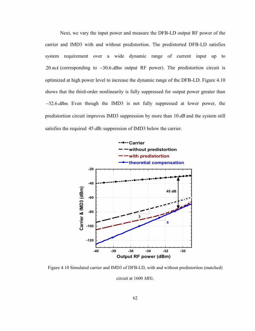
62
Next, we vary the input power and measure the DFB-LD output RF power of the
carrier and IMD3 with and without predistortion. The predistorted DFB-LD satisfies
system requirement over a wide dynamic range of current input up to
20 mA (corresponding to 30.6 dBm output RF power). The predistortion circuit is
optimized at high power level to increase the dynamic range of the DFB-LD. Figure 4.10
shows that the third-order nonlinearity is fully suppressed for output power greater than
32.6 .dBm Even though the IMD3 is not fully suppressed at lower power, the
predistortion circuit improves IMD3 suppression by more than 10 dB and the system still
satisfies the required 45 dBc suppression of IMD3 below the carrier.
-120
-100
-80
-60
-40
-20
-40 -38 -36 -34 -32 -30
Carrier
without predistortion
with predistortion
theoretial compensation
Carr
ier
& I
MD
3 (
dB
m)
Output RF power (dBm)
5
3
45 dB
Figure 4.10 Simulated carrier and IMD3 of DFB-LD, with and without predistortion (matched)
circuit at 1600 MHz.

63
Furthermore, the performance of the predistortion circuit is simulated for
broadband operation with a two-tone signal input. The frequency spacing between the
two tones is kept at 4 MHz and the operation frequency of the first tone is swept from 0.7
to 2.5 GHz in steps of 100 MHz. The results of theoretical analysis using nonlinear
transmission coefficients are plotted in Figure 4.11. Theoretically, the IMD3/C can be
improved by 13.4 dB at 16 mA current input power level. With the predistortion circuit,
the IMD3/C is improved by 15 dB at 700 MHz and 10 dB at 2500 MHz. This is because
the theoretical analysis of the predistortion circuit transfer function is limited to the third-
order nonlinearity with frequency independent coefficients. The simulated predistortion
circuit cancels some IMD3 terms generated by higher order nonlinearity. The poor
performance of the predistortion circuit at high frequency may be due to the high
insertion loss at high frequency, the matching circuit and the presence of nonlinear
parasitic capacitance that increases the phase shift between the carrier and IMD3 [34-35].
The parasitic capacitance of MOSFET is usually nonlinear. Nonlinear capacitors increase
the phase shift between signal carrier and distortion terms with the increase of operation
frequency.

64
-55
-50
-45
-40
-35
800 1200 1600 2000 2400
without predistortion
theoretical cancellation
with predistortion
IMD
3/C
arr
ier
(dB
c)
Frequency (MHz)
Figure 4.11 Simulated IMD3/C of DFB-LD, theoretical analysis, with and without predistortion
(matched) from 0.7 to 2.5 GHz.
We compared the distortion suppression with matched and unmatched
predistortion circuit. The unmatched predistortion circuit only contains the distortion
generation block. The CCC-CG matching network degrades IMD3 cancellation, as
depicted in Figure 4.12. The effect of the nonlinear parasitic capacitance that increases
the phase shift between carrier and IMD3 is evident in Figure 4.13 for the unmatched
predistortion circuit. The matching network generates some distortion products and
increases the phase mismatch between the carrier and IMD3 as shown in Figure 4.13.
These distortion products are amplified by the distortion generation block along with the
carriers and are sent to the DFB-LD. When these amplified distortion products are
comparable with the ones generated by the distortion generation block only, they interact
destructively and reduce the amount of IMD3 input to the DFB-LD to suppress its third-
order nonlinearity. To reduce the nonlinearity effect caused by the CCC-CG matching
network, the triplet-core circuit is tuned to generate more distortion signal.

65
-60
-55
-50
-45
-40
-35
800 1200 1600 2000 2400
without predistortion
theoretical analysis
matched predistortion
unmatched predistortion
IMD
3/C
arr
ier
(dB
c)
Frequency (MHz)
Figure 4.12 Simulated IMD3/C with matched and unmatched predistortion circuit.
2
4
6
8
10
12
14
16
18
800 1200 1600 2000 2400
matched predistortion
unmatched predistortion
Ph
as
e (
de
gre
e)
Frequency (MHz)
Figure 4.13 Simulated phase difference between signal carrier and IMD3 with matched and
unmatched predistortion circuit.
4.3.2 Tuneability Evaluation
Another advantage of this predistortion circuit is that the generated IMD3 can be varied
by up to 10 dB by tuning the bias current I2 and I3. For effective third-order nonlinearity

66
suppression of a DFB-LD, there is a required amount of IMD3 to be generated by the
predistortion circuit at the input of DFB-LD. The nonlinearity of the triplet-core circuit
was discussed in Section 2.3.3. As we shown, tuning the bias current of differential pairs
would change the nonlinearity of the entire transconductance. Adjusting the bias current
should keep the active current mirrors in saturation.
Figure 4.14 is plotted by feeding the output current of the predistortion circuit to a
50 load. The bias current I1 and I3, I2 of the proposed triplet-core circuit can be tuned
by adjusting the bias current of M16 and M17 (refer to Figure 4.2 for more information).
Since I1 and I2 can be tuned from 2.6 ~ 3 mA and 0.8 ~ 2 mA while the current mirror ratio
of M16/M1C and M16/M2C are 1/2 and 1, respectively. Correspondingly, the bias currents
Ib2 and Ib3 of the predistortion circuit can be adjusted from 1.3 ~ 1.5 mA and 0.8 ~ 2 mA
respectively. IMD3 can be increased by reducing Ib2 or increasing Ib3. The highest
dynamic range of IMD3 is obtained when Ib2 is 1.3 mA and Ib3 is 2 .mA The strong
tuneability enables the predistortion circuit to correctly linearize some unknown LD
sources.

67
-60
-50
-40
-30
-20
-10
0
10
20
0 2 4 6 8 10
Carrier
I2, I3 (1.3 mA, 0.8 mA)I2, I3 (1.5 mA, 0.8 mA)I2, I3 (1.5 mA, 2 mA)I2, I3 (1.3 mA, 2 mA)
Carr
ier
an
d IM
D3 (
dB
m)
Output power (dBm)
Figure 4.14 Simulated output power of the predistortion circuit for different bias currents Ib2 and
Ib3.
4.4 Comparison of This Work with Previous Predistortion
Comparing the designed amplifier-based predistortion with the most recently published
predistortion in circuit level [2, 7-10], this work has three advantages. First, the designed
predistortion circuit achieves 6 ~ 15 dB IMD3 suppression over a broadband operation,
from 700 MHz to 2500 MHz. The IMD3 suppression of this predistortion circuit is
comparable with [8], which is designed for a single operation frequency. Second, the
designed amplifier-based predistortion circuit uses a single path to predistort and amplify
the signal. Contrasting to the multi-path configuration in [2, 7-10], this design has a
simple structure. Third, as opposed to the voltage-mode currently reported CMOS

68
predistortion circuit [7, 10], the designed predistortion is a current-mode approach which
supplies directly current source to the LD. Although the predistortion circuit in [8] is a
current approach, our design can supply higher modulation current and operate in much
broader bandwidth. Table 4.2 shows a comparison of this work and recently published
predistortion circuit.
Table 4.2 Comparison of previously published predistortion design
Tech.
Operating Frequency (MHz)
IMD3 Suppression (dB)
Complexity
This work 90 nm CMOS 700 ~ 2500 6~15 Low
[10] 0.18 µm CMOS 1850 ~ 2150 5~10 High
[9] Not reported 5800 16 High
[8] 0.35 µm CMOS 1350 12 High
[7] 0.18 µm CMOS 50 ~ 500 5~10 High
[2] Not reported
370 ~ 480 820 ~ 960
1710 ~ 1980 6~10 High
4.5 Conclusion
In this chapter, detailed information of the circuit design is introduced. The predistortion
circuit consists of basic, cascode and active current mirror networks. The current
injection technique significantly improves the efficiency of current amplification and
reduces power dissipation. The predistortion IC supplies a modulation signal of up to
25 mA and bias current of 110 mA with 200 mW of power consumption. The equivalent
transconductance of the predistortion IC is 0.64 S. The predistortion circuit is simulated

69
using Cadence Virtuoso Spectre circuit simulator. The designed predistortion achieves
more than 10 dB improvement from 0.7 to 2.5 GHz. By adjusting the bias currents, the
IMD3 can be shifted 10 dB , which is suitable to linearize other LDs.

70
CHAPTER 5 CONCLUSION
5.1 Conclusion
In wireless access networks, RoF systems have the highest potential to satisfy large
capacity, high speed and cost effective requirements. However, the nonlinearity
introduced by optical modulators’ response significantly distorts RoF transmission.
Among currently available linearization techniques, predistortion is selected to linearize
the DFB-LD.
In this thesis, an amplifier-based tuneable RF predistortion IC solution is
investigated and designed using TSMC 90 nm technology. The complete circuit includes
a triplet-core circuit, matching networks and current mirror designs. The IC supplies up
to 25 mA modulation current and 110 mA bias while consuming 200 .mW It is capable
of suppressing IMD3 up to 15.4 dB compared to the free-running DFB-LD at
16 mA signal amplitude input. The frequency of operation ranges from 0.7 to 2.5 GHz.
The presented predistortion circuit is the first gain boosting IC solution which
provides a cost effective approach. The designed predistortion circuit does not require
external amplifiers or phase shifters because they would introduce undesired IMD3 and
limit the operation bandwidth. Also, the gain boosting predistortion circuit makes it
possible to remove the LNA which is the block just before the modulator. Thirdly, the IC
is broadband matched without using inductors. Inductors take up a large amount of chip
area. Therefore, the predistortion IC solution reduces system cost significantly.

71
5.2 Future Work
The future results of extensive research done on the predistortion IC are described:
The IC layout and fabrication are the first considerations. Since the input has a
fully differential configuration, careful design is necessary to ensure symmetry of the
CCC-CG stage and to the input path of the triplet-core circuit. Also, the symmetrical
parts of LNA and active current mirrors have to be matched. Otherwise, the different
signal delay will diminish the capability of IMD3 suppression.
The second consideration involves testing the chip. It is necessary to design a
PCB which includes a broadband 1800 hybrid coupler and two off-chip 20 pF capacitors.
The 1800 hybrid coupler converts the single ended input RF signal to differential inputs.
The differential signals are coupled to the predistortion IC using two 20 pF capacitors.
To reduce the interconnection loss between the predistortion IC and DFB-LD, the two
blocks are placed physically close and a bonding wire is used to connect them together.
The third consideration involves the proposed approach to improving the system’s
stability. As we know, the laser’s band gap changes with temperature and thermal
expansion and hence, varies the nonlinearity of LDs. Therefore, an adaptive temperature
control circuit would enhance its temperature tolerance. In the future, instead of using
discrete devices, the predistortion IC and DFB-LD can be fabricated in one package.
Therefore, the cascaded commercialized modulator can provide a much more linear
transmission in RoF systems.
Last but not the least, more advanced TSMC technologies, like 65 nm, 40 nm or
28 nm can be used to design a high frequency, Ultra-Wideband and low power analog

72
predistortion IC. Additionally, an automatic gain control LNA can be designed to
regulate the signal input to the distortion generation block. Also, the predistortion circuit
can be modified to linearize power amplifiers (PAs) and other modulators as well.
73
REFERENCES
[1] Ng’oma, “Radio-over-Fibre Technology for Broadband Wireless Communication
Systems,” Ph.D. thesis, Electrical Engineering, Eindhoven Univ., pp. 19, 2005.
[2] L. Roseli, V. Borgioni, F. Zepparelli, F. Ambrosi, M. Comez, P. Faccin, and A.
Casini, “Analog Laser Predistortion for Multiservice Radio-Over-Fiber Systems,”
IEEE J. of Lightwave Technol., vol. 21, pp. 1211 – 1223, May 2003.
[3] R.E. Schuh and D. Wake, “Distortion of W-CDMA signals over optical fiber links,”
in Int. Top. Meeting Microwave Photonics Tech. Dig. (MWP’99), Melbourne,
Australia, Nov. 1999, pp. 9-12.
[4] B. Masella and X. Zhang, “Linearized optical single-sideband Mach-Zhender
modulator for radio-over-fiber systems,” IEEE Photon. Technol. Lett., vol. 19, pp.
2024-2026, Dec. 2007.
[5] S.H. Lee, J.M. Kang, I.H. Choi, and S.K. Han, “Linearization of DFB laser diode by
external light-injected cross-gain modulation for Radio-over-Fiber Link,” IEEE
Photon. Technol. Lett., vol. 18, pp. 1545-1547, July, 2006.
[6] T. Ismail, C. Liu, J.E. Mitchell, and A.J. Seeds, “High-Dynamic-Range Wireless-
Over-Fiber Link Using Feedforward Linearization,” IEEE J. of Lightwave Technol.,
vol. 25, pp. 3274-3282, May. 2003.
[7] R. Sadhwani and B. Jalali, “Adaptive CMOS Predistortion Linearizer for Fiber-Optic
Links,” IEEE J. of Lightwave Technol., vol. 21, pp. 3180-3193, Dec. 2003.

74
[8] F. C. Lin, D. M. Holburn, V. A. Lalithambika, R. J. Mears, C. H. Hum and S. D.
Wlaker, “A CMOS predistortion circuit for wideband optical fibre links,” in IEEE
CCECE, vol. 1, May 2004, pp. 245-248.
[9] H. H. Lu, S. J. Tzeng and Y. L. Liu, “Intermodulaltion distortion suppression in a
full-duplex Radio-over-Fiber ring network,” IEEE Photon. Technol. Lett., vol. 16,
pp. 602-604, Dec. 2004.
[10] Z. Xu and L. MacEachern, “A predistortion circuit design technique for high
performance analog optical transmission,” in IEEE MNRC, 2008, pp. 213-216.
[11] Y. Shen, B. Hraimel, Xiupu Zhang, G. Cowan, K. Wu, and T. Liu, “A novel analog
broadband RF predistortion circuit to linearize electroabsorption modulator in
multiband OFDM ultra-wideband radio over fiber systems,” IEEE Trans.
Microwave. Theory Tech., vol. 58, no.11, pp. 3327 - 3335, 2010.
[12] Charles H. Cox, Edition III, Analog Optical Links Theory and Practice, Chapter 6,
Cambridge Univ. Press, 2004.
[13] B. H.T. Lin, and Y. H. Kao, “Nonlinear distortions and compensation of DFB laser
diode in AM-VSB lightwave CATV applications,” IEEE J. of Lightwave Technol.,
vol. 14, pp. 2567 – 2574, Nov. 1996.
[14] J. Lipson, L. C. Upadhyayula, S. Y. Huang, C. B. Roxlo, E. J. Flynn, P. M. Nitzsche,
C. J. McGrath, G. L. Fenderson and M. S. Schaefer, “High-fidelity lightwave
transmission of multiple AM-VSB NTSC signals,” IEEE Trans. Microwave. Theory
Tech., vol. 38, no.5, pp. 483 - 493, May 1990.
75
[15] T. W. Kim, B. Kim and K. Lee, “High linear receiver front-end adopting MOSFET
transconductance linearization by multiple gated transistors,” IEEE J. of Solid-State
Circuit, vol. 39, pp. 223 – 229, Jan. 2004.
[16] M. Parvizi and A. Nabavi, “Improved dericative superposition scheme for
simultaneous second- and third-order distortion cancellation in LNAs,” IET J.
Electronics Lett., vol. 45, pp. 1323 – 1325, Dec. 2009.
[17] V. Aparin and L. E. Larson, “Modified derivative superposition method for
linearizing FET low-noise amplifier,” IEEE Trans. Microwave. Theory Tech., vol.
53, pp. 571 - 581, Feb. 2005.
[18] B. Razavi, “Passive and active current mirrors,” in Design of analog CMOS
integrated circuits, New York, USA, McGraw-Hill, pp. 135 – 151, 2001.
[19] S. T. Dupuie and M. Ismail, “Highfrequency CMOS transconductors,” in Analogue
IC design: the current-mode approach, Herts, U. K., Peter Peregrinus, pp. 181 -237,
1990.
[20] L. Bisdounis, “Short-circuit energy dissipation model for sun-100nm CMOS
buffers,” in IEEE ICECS, 2010, pp. 615-618.
[21] B. Gilbert, “The Multi-tanh principle: A tutorial overview,” IEEE J. of Solid-State
Circuit, vol. 33, no. 1, pp. 2 – 17, Jan. 1998.
[22] A. Bevilacqua and A. M. Niknejad, “An ultrawideband CMOS low-noise amplifier
for 3.1-10.6-GHz wireless receivers,” IEEE J. Solid-State Circuits, vol. 39, no. 12,
pp. 2259 – 2268, Dec. 2004.

76
[23] A. Bevilacqua, C. Sandner, A. Gerosa, and A. Nevani, “A fully integrated
differential CMOS LNA for 3-5-GHz ultrawideband wireless receivers,” IEEE
Microwave and Wireless Components Lett., vol. 16, pp. 134-136, Mar. 2006.
[24] S. S. K. Ho, and C. E. Saavedra, “A CMOS broadband low-noise mixer with noise
cancellation,” IEEE Trans. Microwave. Theory Tech., vol. 58, no. 5, pp. 1126 – 1132,
May 2010.
[25] T. H. Lee, “Noise,” in The design of CMOS radio frequency integrated circuits, New
York, USA, Cambridge University Press, 1998.
[26] H. T. Friis, “Noise figure of radio receivers,” in Proc. IRE, vol. 32, July 1944,
pp.419-422.
[27] W. Zhuo, S. Embabi, J. Gyvez, and E. Sanchez-Sinencio, “Using capacitive cross-
coupling technique in RF low-noise amplifiers and down-conversion mixer design,”
in Proc. Eur. Solid-State Circuits, pp. 116–119, Sep. 2000.
[28] W. Zhuo, X. Li, S. Shekhar, S. H. K. Embabi, J. Pineda de Gyvez, D. J. Allstot, and
E. Sanchez-Sinencio, “A capacitor cross-coupled common-gate low-noise
amplifier,” IEEE J. Trans. on circuit and systems, vol. 52, Dec. 2005.
[29] X. Li, S. Shekhar and D. J. Allstot, “Gm- Boosted Common-Gate LNA and
Differential Colpitts VCO/Q VCO in 0.18-μm CMOS,” IEEE J. Solid-State Circuit,
vol.40, pp. 2609-2619, Dec. 2005.
[30] K. Kundert, “A test bench of differential circuits”, [Online] available:
http://www.designers-guide.org/Analysis/diff.pdf
[31] K. Kundert, “Measuring S-parameter of a differential mixer”, [Online] available:
http://www.designers-guide.org/Analysis/diff-sp.pdf
77
[32] L. A. MacEachern and T. Manku, “A charge-injection method for Gilbert cell
biasing,” in IEEE CCECE, vol. 1, 1998, pp 365-368.
[33] K. Xuan, K. F. Tsang, and S. C. Lee, and W. C. Lee, “A current bleeding mixer based
on Gilbert-cell featuring LO amplification,” in IEEE SOCC, 2009, pp 137-140.
[34] S. A. Maas, “Volterra-Series and Power-Series Analysis,” in Nonlinear microwave
and RF circuits, Boston, London, Artech house, pp. 215 – 276, 2003.
[35] C. Crespo-Cadenas, J. Reina-Tosina, and J. Madero-Ayora,“Phase characterization of
two-tone intermodulation distortion,” in IEEE MTT-S international conference, 2005.