AMC: Advanced Multi-accelerator Controller · AMC: Advanced Multi-accelerator Controller...
33
AMC: Advanced Multi-accelerator Controller 1,2 ,Tassadaq Hussain, 3 ,Amna Haider, 3 Shakaib A. Gursal, and 1 Eduard Ayguad´ e 1 Barcelona Supercomputing Center , 2 BSC-Microsoft Research Centre , 3 Unal Center of Engineering Research & Development Barcelona, Spain {tassadaq.hussain, eduard.ayguade} @bsc.es {first name}@ucerd.com Abstract The rapid advancement, use of diverse architectural features and introduction of High Level Synthesis (HLS) tools in FPGA technology have enhanced the ca- pacity of data-level parallelism on a chip. A generic FPGA based HLS multi- accelerator system requires a microprocessor (master core) that manages memory and schedules accelerators. In a real environment, such HLS multi-accelerator sys- tems do not give a perfect performance due to memory bandwidth issues. Thus, a system demands a memory manager and a scheduler that improves performance by managing and scheduling the multi-accelerator’s memory access patterns effi- ciently. In this article, we propose the integration of an intelligent memory system and efficient scheduler in the HLS-based multi-accelerator environment called Advanced Multi-accelerator Controller (AMC). The AMC system is evaluated with memory intensive accelerators, High Performance Computing (HPC) appli- cations and implemented and tested on a Xilinx Virtex-5 ML505 evaluation FPGA board. The performance of the system is compared against the microprocessor- based systems that have been integrated with the operating system. Results show that the AMC based HLS multi-accelerator system achieves 10.4x and 7x of speedup compared to the MicroBlaze and Intel Core based HLS multi-accelerator systems. 1. Introduction In the last few years the density of FPGAs [1, 2] and performance per watt [3] have improved, which allows the High Performance Computing (HPC) industry to increase and provide more functionalities on a single chip. 3D ICs [4] open Preprint submitted to Parallel Computing May 7, 2015
Transcript of AMC: Advanced Multi-accelerator Controller · AMC: Advanced Multi-accelerator Controller...

AMC: Advanced Multi-accelerator Controller
1,2,Tassadaq Hussain, 3,Amna Haider, 3Shakaib A. Gursal, and 1Eduard Ayguade1 Barcelona Supercomputing Center , 2BSC-Microsoft Research Centre ,
3Unal Center of Engineering Research & DevelopmentBarcelona, Spain
{tassadaq.hussain, eduard.ayguade}@bsc.es{first name}@ucerd.com
Abstract
The rapid advancement, use of diverse architectural features and introduction ofHigh Level Synthesis (HLS) tools in FPGA technology have enhanced the ca-pacity of data-level parallelism on a chip. A generic FPGA based HLS multi-accelerator system requires a microprocessor (master core) that manages memoryand schedules accelerators. In a real environment, such HLS multi-accelerator sys-tems do not give a perfect performance due to memory bandwidth issues. Thus, asystem demands a memory manager and a scheduler that improves performanceby managing and scheduling the multi-accelerator’s memory access patterns effi-ciently. In this article, we propose the integration of an intelligent memory systemand efficient scheduler in the HLS-based multi-accelerator environment calledAdvanced Multi-accelerator Controller (AMC). The AMC system is evaluatedwith memory intensive accelerators, High Performance Computing (HPC) appli-cations and implemented and tested on a Xilinx Virtex-5 ML505 evaluation FPGAboard. The performance of the system is compared against the microprocessor-based systems that have been integrated with the operating system. Results showthat the AMC based HLS multi-accelerator system achieves 10.4x and 7x ofspeedup compared to the MicroBlaze and Intel Core based HLS multi-acceleratorsystems.
1. Introduction
In the last few years the density of FPGAs [1, 2] and performance per watt [3]have improved, which allows the High Performance Computing (HPC) industryto increase and provide more functionalities on a single chip. 3D ICs [4] open
Preprint submitted to Parallel Computing May 7, 2015

another dimension in the HPC industry that emulate three-dimensional stackedchips by rapidly reconfiguring their two-dimensional fabrics in a third spatial di-mension of time/space. Such devices have the power to reconfigure their fabricup-to 1.6 billion times per second [4]. The Stacked Silicon Interconnect (SSI) [5]technology provides another dimension to high-density FPGAs that satisfies theneeds of on-chip resources for HPC system. SSI combines two or more FPGAsfor larger and complex systems. As the designs grow larger and complex, thechances of error and complexity increase, thus demands an abstract level designmethodology.
Time is indeed changing the way HPC systems are designed. Now the HPCindustry wants to execute multi-applications for optimal performance. This de-mands a design environment which has dense and flexible hardware consumesless power and has abstract-level programming tools. Reducing design time andthe size of the team are crucial. Numerous architectures (RISC, CISC), designmethodologies (SoC, MPSoc), and programming tools (OpenMP, MPI) are avail-able in the HPC domain. These systems do not give a perfect performance due tothe processor-memory speed gap [6, 7] given by the formulaA T = Prob ∗ OnChipMemory + (1 − Prob ) ∗ [On/Offchipbus + DRAM ]t .
The Access Time (AT) depends upon the probability (Prob) to access data from dif-ferent units such as On Chip Memory (On-Chip data arrangement and probabil-ity of reuse), on/offchipbus (flow control, arbitration, translation, interconnection)and DRAMt (bank, column and row selection).
Over the past few years, HLS tools have been strengthened and become trulyproduction-worthy [8] by supporting fundamental technologies such as pipelin-ing and FSM. Initially confined to data path designs, HLS tools are now com-menced to address complete systems, including control logic, complex on-chipand off-chip interconnections. HLS [9] tools provide design modeling, synthesis,and validation at a higher level of abstraction. This makes computation cheaper,smaller, and less power hungry, thus enabling more sophisticated system designfor complex HPC applications. HLS-based multi-accelerator systems always re-quire a master processor core which perform memory management, data transferand scheduling of the multi-accelerator. The master core adds overhead of ad-dress/data management, bus request/grant and external memory access time.
To improve HLS-based multi-accelerator system performance an intelligentcontroller is needed that has efficient on-chip Specialized Memory and data man-agement, an intelligent front-end/back-end scheduler and a fast I/O link and sup-ports programming model that manages memory accesses in software so that hard-ware can best utilize them. We implement such a controller in hardware called
2

Advanced Multi-accelerator Controller (AMC), some salient features of the pro-posed AMC architecture are given below:
• The AMC based system can operate as a stand-alone system, without sup-port of the master cores and operating system (OS).
• The AMC provides specialized on-chip (1D/2D/3D) memory that improvessystem performance by prefetching complete data sets.
• Complex access patterns are described using single or multiple descriptors,thus reduces the on-chip communication time.
• It handles multiple HLS hardware accelerator IPs using an event-drivenhandshaking methodology; this decreases the time-to-market and complex-ity of hardware.
• The AMC schedules multi-accelerator requests while taking into accountboth the processing and memory requirements defined at program-time. Atrun-time, the AMC back-end scheduler reorders accelerator’s memory re-quests considering SDRAM open banks. This removes the overhead fromopening/closing rows/banks and idle cycles on the data bus.
• Standard C/C++ language calls are supported to program multi-acceleratortasks in software.
Section 2 discusses the HLS-based system. Section 3 describes the AMC sys-tem and Section 4 explains how it is used. Section 5 introduces the experimentalframework and Section 6 presents the results. Section 7 discusses the related workand finally Section 8 provides the conclusions.
(a) (b)
Figure 1: (a) Generic High Level Synthesis Multi-Accelerator System (b) High Level SynthesisTool Design Flow
3

2. High Level Synthesis Multi-accelerator System
In this section, we discuss High-Level Synthesis (HLS) system design toolsand working operation. The HLS tool takes algorithm level behavioral specifica-tion of a system and generates a register-transfer level structure that implementsthat behaviour. The HLS-based multi-accelerator system is shown in Figure 1 (a).The HLS system is further categorized into three sections the Master Core, theHLS tools and the SDRAM controller.
2.1. Master CoreA Master Core (CPU) is capable of initiating data transfer on the bus for
multi-accelerator (slave). The core is responsible for memory management andscheduling of HLS multi-accelerator system. It decides when an accelerator startexecution and provides a I/O link. All accelerators can communicate with eachother via Master core. The HLS system does not get optimum performance ifaccelerators are not tightly scheduled.
2.2. High Level Synthesis ToolIn this section, we explain existing HLS tool and their basic operation. Trans-
lation of HPC algorithms into hardware is difficult and time-consuming. Largeapplication result in big systems with higher chances of failure and complexity inthe scheduling and reuse of resources. To control the size and complexity of suchapplications, system designers are required to perform design modeling, synthe-sis, and validation at a higher level of abstraction. Ylichron (now PLDA Italia)provides a source-to-source C to VHDL compiler toolchain targeting system ar-chitects called HCE (Hardware Compiling Environment) [10]. ROCCC 2.0 [11] isa free and open source tool that focuses on FPGA-based code acceleration from asubset of the C language. ROCCC tries to utilize parallelism within the constraintsof the target device, optimize clock cycle time by pipelining, and minimizes area.
A generic HLS toolchain takes ANSI-C language as input, which representsthe hardware architecture with some restrictions and extensions. The design flowconsists of a series of steps (see Figure 1 (b)), with each step transforming theabstraction level of the algorithm into a lower level description. The HLS toolfirst extracts the Control and Data Flow Graph (CDFG) from the application tobe synthesized. The CDFGs describe the computational nodes and edges betweenthe nodes. Tool provides different methods to explore the CDFG of the inputalgorithm and generates the data-path structure. The generated data-path struc-ture contains the user-defined number of computing resources for each computing
4

node type and the number of storage resources (registers). The Allocation andScheduling step maps the CDFG algorithm onto the computing data-path and pro-duces a Finite State Control Machine. The Refine step uses the appropriate BoardSupport Package and performs synthesis for the communication network. Finally,the VHDL-RTL generation step produces the VHDL files to be supplied to theproprietary synthesis tools for the targeted FPGA.
2.3. SDRAM ControllerIn this section, we describe basic parameters and working operation of Syn-
chronous Dynamic Random Access Memory (SDRAM). SDRAM is dynamic ran-dom access memory (DRAM) that is synchronized with the processor system bus(shown in Figure 1 (a)). The parameters nbanks, wmem, fmem, dr, and BL areused to describe the SDRAM memory architecture. Where nbanks stands for thenumber of banks, wmem is the width of the data bus in bytes, fmem representsthe clock frequency of memory in MHz, dr defines the number of data words thatcan be transferred during a clock cycle, and BL is the word length of programmedburst. To control the SDRAM system, specific commands are sent to the memoryport according to the protocol. The SDRAM communications protocol includessix command signals which are activate (ACT), read (RD), write (WR), precharge(PRE), refresh (REF), and no-operation (NOP). The activate command is suppliedwith a row and a bank as an argument, informs the selected bank to copy the re-quested row to its row buffer. Once the requested row is opened, column can beaccessed by read and write bursts having burst length (BL) of 4 or 8 words. Theread and write commands include separate bank, row, and column address lines.The precharge command corresponds the activate command to place the contentsof the row buffer back to its location in the memory. An auto-precharge flag witha read and write command is inserted to automatically precharge at early possiblemoment after the data transfer. This gives the benefits to an upcoming schedulingrow to be opened as quickly as possible without causing contention on shared sys-tem bus. To prevent the data loss by capacitor leakage, a refresh command mustconstantly be issued. For entire memory array, multiple refresh commands arerequired.
3. Advanced Multi-Accelerator Controller
In this section, we describe the Advanced Multi-Accelerator Controller (AMC)system (shown in Figure 2) for HLS tool. The architecture is based on five units:
5

Figure 2: Architecture of Advanced Multi-Accelerator Controller Based System
the Input/Output link, the Memory Architecture, the Memory Manager, the Sched-uler and the SDRAM Controller.
3.1. Input/Output LinkThe Input/Output (I/O) link provides an interface between AMC and HLS
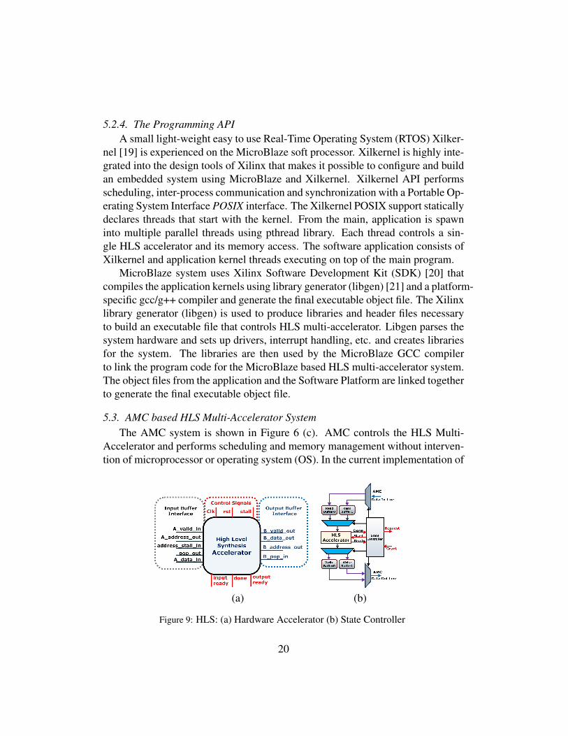
multi-accelerator unit. The I/O link as shown in Figure 2 is used to read/writehigh-speed data to/from register memory of HLS multi-accelerator. Transfer ofdata is accomplished according to the system clock. The AMC Input/Output (I/O)link has a peak bandwidth of 1.6 GB/s as it operates at maximum 200 MHz clockhaving data bus width of 64-bit. A state controller (Figure 9 (b)) is integrated witheach hardware accelerator to manage multiple buffers. The state controller takesaccelerator data requests and manages multiple buffers using request and grantsignals.
3.2. Memory ArchitectureA reliable and efficient memory architecture is required for any application
being programmed for HLS multi-accelerator system. The AMC memory archi-tecture is divided into two sections the Descriptor Memory and the Data Memory.
3.2.1. Descriptor MemoryThe AMC descriptor memory holds the information of multi-accelerator mem-
ory access patterns and scheduling methodology. The descriptor memory is fixedlength data word with a number of attribute fields that describe the access pat-tern. A single descriptor describes the access pattern of a strided stream, andmultiple descriptors are used to define complex memory patterns. The least set ofparameters for the memory descriptor block, includes command, source address,destination address, stride, stream and priority. Command specifies whether to
6

r e c e i v e ( /∗ Loca l Address ∗ / 0 x00000000 , /∗ E x t e r n a l Address ∗ / 0 x00000100 ,/∗ P r i o r i t y ∗ / 0x00 , /∗ Stream ∗ / 0x08 , /∗ S t r i d e ∗ / 0x00 ) ;
Figure 3: AMC Function Call: Single Descriptor Program
read/write a single element or a stream of data. The address parameters specify thestarting addresses of the source and destination locations. Stride indicates the dis-tance between two consecutive physical memory addresses of a stream. The pri-ority describes the selection and execution criteria of an accelerator. The programstructure of AMC is stack based where descriptor holds information of completememory access pattern. The machine code of AMC consists of just an opcode thatactivate/deactivate accelerator kernel. Memory management and optimization forrepeated memory access is done at compile time and are executed in hardware atruntime. The proposed AMC system provides C and C++ language support thatinitializes descriptor blocks. The program example of a single memory access ispresented in Figure 3. The local address and external address parameters hold thestart address of specialized (buffer) memory and main memory (SDRAM) data setrespectively. The Priority defines the order in which memory access is entitled tobe process. The parameters Stream and Stride define the type of memory access.The value 0x08 and 0x00 of Stream and Stride parameters respectively initial-izes AMC to access a stream of 8-words with a unit stride. At run-time, the AMCaccesses 32-bit word from the 0x00000100 address location of main memoryand write it to the 0x00000000 address location of Specialized Memory. Thefollowing memory access till the end of a stream, the AMC generates main mem-ory address by taking the address of main memory from the previous access andadds stride (0x08) value. The Specialized Memory address is sequential (con-tiguous) and requires unit increment.
3.2.2. Data MemoryTo achieve high performance from any computing unit, analysis of the data
transfer through the algorithm and placement on underlying memory architectureis required. The AMC underlying data memory structure is shown in Figure 5,The data memory of AMC system is further subdivided into three sections whichare: the Register Memory, the Specialized Memory and the Main Memory.
7

(a) (b) (c)
Figure 4: AMC: (a) Dataset/Program Code (b) Three Dimension Specialized Memory Architec-ture (c) (3 x (n x 2) + 1) n-Stencil
Register Memory. The Register Memory is fast and efficient as it provides paral-lel/patronized data access in a single cycle to the accelerator. The register memoryresides on the same hardware of processing unit and uses FPGA resources/slicesthat have multiple small independent memory register arrays. The HLS tools(such as ROCCC [11] & HCE [10]) can automatically solve memory bottleneckproblems by splitting, interleaving, or reorganizing registers that reuse the portionof data. The HLS tools interleave and reorganize the register memory that rear-range sequential data storage into two or more non-contiguous storage blocks andprovide single cycle access.
Specialized Memory. The application’s dataset placed on main memory (SDRAM)has a linear structure. Hence, it is critical to keep the application’s dataset accesslatency much lower than the main memory. The Specialized Memory (Figure 4(b)) structure is used to reduce SDRAM access latency and provide parallel read-/write accesses to compute units. The Specialized Memory architecture is an arrayof dual port Static RAM cells which are tightly coupled and mapped according tothe accelerator’s access patterns and can be shared between more than one acceler-ators by the memory management unit 3.3. The Specialized Memory access is fastas register memory and is physically organized into multi dimension (1D/2D/3D)architecture. One application kernel can access complete row, column or block ofSpecialized Memory. The memory specified for one accelerator can be accessibleto another accelerator if data reuse is required.
The program structure that is used to initializes Specialized Memory into 1D,2D or 3D structure is shown in Figure 4 (a). The Buffer Width describes the sizeof row Nx (1D buffer). The Buffer Dimension explains the dimensions (2D/3D)
8

(Nz and Ny) of the memory block. Nx and Nz define the sizes of each block (Ny).The size of block (Nx, Nz) is selected to fit in one BRAM of the target device. Thecurrent AMC Specialized Memory architecture is composed of single or multipleBRAM18 (1x18 Kb) blocks. Depending upon the dimension of Specialized Mem-ory (Nx, Nz) (rows, column) the memory block can be configured as, 1x16k,2x8k, 4x4k, 8(9)x2k or 16(18)x1k. A master port (M) is used to trans-fer streaming data between main memory unit and Specialized Memory.
For example, a 3D Specialized memory architecture for generic stencil dataaccess is shown in Figure 4 (b). Each bank of Specialized memory has two ports(PortA & PortB) which allows the compute unit to perform parallel read/writedata to/from multiple banks. The on-chip encapsulation of data memories withprocessing units allows application kernels to access data without extra delay.The generic stencil structure is shown in Figure 4 (c). When n=4, 25 points arerequired to compute one central point. This means, to compute a single elementeight points are required in each of x, y and z directions, as well as one centralpoint. The 3D-stencil (when n = 4) occupies 9 different banks to place it onSpecialized Memory. The central, x and z points are placed on the same bank(y),and each y-point needs a separate bank (y+4 to y-4). The Specialized Memorytakes 9 cycles ((2 points/bank)/cycle) to transfer 17 points of bank(y) and 1 pointeach from bank(y+4) to bank(y-4). Each bank read/write operation is independentto other and can be performed in parallel. Therefore, the Specialized Memorytakes nine cycles to transfer 25 points of single stencil. To utilize all bank andto reduce access time multiple 3D-Stencils are placed on 3D Specialized Memory(Figure 5 (b).
Global Memory. The slowest type of memory in the AMC system is the globalmemory, which is the main memory (SDRAM), and is accessible by the wholesystem. Even though, AMC has an efficient way of accessing main memory thatbest utilizes the bandwidth, it still has latency with respect to other memory sys-tems (discussed in section 3.5).
3.3. Memory ManagerTo achieve maximum memory bandwidth, the AMC organises complex ac-
cess pattern in single or multiple descriptors at compile-time. At run-time, theAMC Memory Manager transfers complete pattern to/from the main memory andSpecialized Memory in multiple noncontiguous strided streams. The AMC Mem-ory Manager has a view of main memory address space that is partitioned into
9

(a) (b)
Figure 5: (a) Memory Hierarchy of AMC System (b) N-Stencil Vector Load & Update Points
segments (shown in Figure 5 (a)). Each segment contains single or multiple de-scriptors that hold the information of specialized and main memory for each ac-celerator. The AMC Memory Manager applies protection at the segment level e.g.a segment can be read/written by the accelerator for which it is allocated. Withina segment, AMC organizes and rearranges multiple noncontiguous memory ac-cesses simultaneously that reduces read/write delay due to the control selection ofSDRAM memory. To reduce false sharing, the Specialized Memory is by defaultdedicated to a single accelerator unit. In the AMC system, the Specialized Memoryis tightly connected to the accelerator that avoids core stalling due to transfer ofmemory content in terms of on-chip communication and SDRAM access latency.AMC keeps the knowledge of memory as to whether or not a certain memory areais in the accelerator’s Specialized Memory. This knowledge allows the AMC tomanage the placement of memory as well as reuses and shares already accessedmemory. The Memory Manager is further divided into two sections which are:the Address Manager and the Data Manager. The Address Manager fetches sin-gle or multiple descriptors depending on the access pattern, translates/reordersin hardware, in parallel with AMC Read/Write operations. The Data Managerimproves the (computedpoint / accessedpoint) (c/a) ratio by organizing and manag-ing the memory accesses. For an accelerator generating single computedpoint, themaximum achievable (ideal) c/a ratio is 1. To provide efficient data access andexcessive reuse, the Data Manager is further divided into three units: the LoadUnit, the Update Unit and the Reuse Unit. The Load unit accesses all point of anaccess pattern, which are required for single Computedpoint. After accessing thefirst access pattern (points), the memory manager transfers control to Reuse unit
10
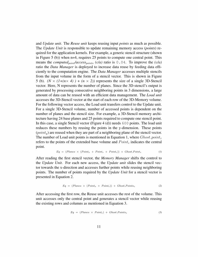
and Update unit. The Reuse unit keeps reusing input points as much as possible.The Update Unit is responsible to update remaining memory access (points) re-quired for the application kernels. For example, a generic stencil structure (shownin Figure 5 (b)) when n=4, requires 25 points to compute one central point. Thismeans the computedpoint/accesspoints (c/a) ratio is 0.04. To improve the (c/a)ratio the Data Manager is deployed to increase data reuse by feeding data effi-ciently to the computation engine. The Data Manager accesses multiple stencilsfrom the input volume in the form of a stencil vector. This is shown in Figure5 (b). (N × (1+(n× 4) ) + (n × 2)) represents the size of a single 3D-Stencilvector. Here, N represents the number of planes. Since the 3D-stencil’s output isgenerated by processing consecutive neighboring points in 3 dimensions, a largeamount of data can be reused with an efficient data management. The Load unitaccesses the 3D-Stencil vector at the start of each row of the 3D-Memory volume.For the following vector access, the Load unit transfers control to the Update unit.For a single 3D-Stencil volume, number of accessed points is dependent on thenumber of planes and the stencil size. For example, a 3D-Stencil memory archi-tecture having 24 base planes and 25 points required to compute one stencil point.In this case, a single Stencil vector (Figure 4 (d)) needs 600 points. The load unitreduces these numbers by reusing the points in the y-dimension. These points(pointy) are reused when they are part of a neighboring plane of the stencil vector.The number of Load unit points is mentioned in Equation 1, where Ghost pointzrefers to the points of the extended base volume and Pointc indicates the centralpoint.
Eq = (Planes × (Pointx + Pointz + Pointc)) + Ghost Pointz (1)
After reading the first stencil vector, the Memory Manager shifts the control tothe Update Unit. For each new access, the Update unit slides the stencil vec-tor towards the x-direction and accesses further points while reusing neighboringpoints. The number of points required by the Update Unit for a stencil vector ispresented in Equation 2.
Eq = (Planes × (Pointx + Pointc)) + Ghost Pointsz (2)
After accessing the first row, the Reuse unit accesses the rest of the volume. Thisunit accesses only the central point and generates a stencil vector while reusingthe existing rows and columns as mentioned in Equation 3.
Eq = (Planes × Pointc) + Ghost Pointsz (3)
11

(a) (b) (c)
Figure 6: AMC: (a) Front-End Scheduler (b) Front-End Scheduling Process (c) Back-End Sched-uler Lookup Table
The Memory Manager improves 3D-Stencil (c/a) ratio. Form the 8-point 3D-Stencil unit, the Memory Manager uses a single input point 25 times before dis-carding it from the internal memory. In practice, this is not achievable due to theghost points (i.e., points belonging to a neighboring tile that are necessary for thecurrent computation) present on the boundaries of the input volume. The MemoryManager improves data reuse ratio for large base volumes.
3.4. SchedulerThe AMC scheduler manages read/write memory accesses and controls oper-
ations of multiple accelerators. The scheduler is categorized into two sections, theFront-End Scheduler and the Back-End Scheduler.
3.4.1. The Front-End SchedulerThe front-end scheduler deals with multi-accelerator execution processes. Each
accelerator requests to access main memory, the front-end scheduler keep placingincoming requests in the buffer. The selection of an accelerator depends on theaccelerator’s request and priority state. The accelerators are categorized into threestates, busy (accelerator is processing on local buffer), requesting (accelerator isfree), and request & busy. In the request & busy state the accelerator is assumedto have double or multi buffers. During this state, the accelerator is processingon one buffer while making requests to fill other. To provide a feature of multi-buffers support in the current developed platform, a state controller (Figure 9 (b))is instantiated with each accelerator that handles the states of accelerator using adouble/multi-buffering technique. The state controller manages the accelerator’sRequest & Grant signals and communicates with the scheduler. Each Request in-cludes a read and write buffer operation. Once the request is accepted, the statecontroller provides a path to the AMC read/write buffer.
12

AMC front-end scheduler supports two scheduling policies, symmetric andasymmetric that execute accelerators efficiently. In Symmetric multi-acceleratorstrategy, the AMC scheduler manipulates the available accelerator’s request inFIFO (First in First out). The Programmed Priority Buffer (Figure 6 (a)) is usedto manage the accelerator’s request in FIFO order. The Asymmetric strategy em-phasizes on priority and incoming requests of the accelerators. The schedulingpolicies are configured statically at program-time and are executed by hardware atrun-time. The number of priority levels can be configured for asymmetric schedul-ing. Assigned priorities of the accelerators are placed in the programmed prioritybuffer (Figure 6 (a)). The comparator picks an accelerator to execute, only if it isready to run, and there are no higher priority accelerators that are in a ready state.If same priorities are assigned for more than one accelerator, AMC scheduler ex-ecutes them as FIFO method. If no scheduling policy is defined for the front-endscheduler, AMC transfers control to the back-end scheduler.
The Front-End Scheduler accumulates requests from the multi-accelerator sys-tem and maintains them in the task buffer (Figure 6 (a)) as per predefined schedul-ing policy. For example, different requests are generated in concurrent order frommultiple sources (Shown in Figure 6 (b)). The Front-End Scheduler takes firstrequest as it is, remaining requests are executed on the priority level defined inProgrammed Priority Buffer. When currently running accelerator process fin-ishes, the AMC does a context switch. Depending upon the scheduling policiesand programme priority buffer, the AMC selects the new accelerator.
3.4.2. The Back-End SchedulerThe AMC Back-End Scheduler employs a strategy that gathers multiple mem-
ory requests, manages them with respect to physical addresses (SDRAM) andmaximizes the reuse of open SDRAM banks that decrease the overhead of open-ing and closing of rows. This strategy imposes conditions on the arrangementof the memory accesses and affects the worst-case latency and gross/net band-width of external memory. The back-end scheduler uses two scheduling rules formemory patterns:
• Patterns are scheduled in a non-blocking manner, which means that a patternthat has been issued cannot be stopped until it has finished access.
• A read or a written pattern scheduled immediately after itself, when thememory is idle. This makes consecutive read and writes accesses indepen-dent of each other, further simplifying back-end scheduling operation.
13

The scheduling of memory accesses is dependent upon the physical address ofcurrent and next transfer. For example, at run-time the Back-End Scheduler gath-ers memory requests from multi-accelerator and place them in Address Look-upTable (shown in Figure 6 (c)). The Address Look-up Table contains unorderedmemory access requests. Each memory access is categorized into four parts i.e.ID, Bank, Row and Column. The ID holds the information of an accelerator andits local memory. The Bank, Row and Column belongs to the physical memory ad-dress space. At run-tome, the Back-End Scheduler schedules memory accesses ofmultiple accelerators by giving highest priority to the bank and row address. Thelookup table executes the AMC policy called bank/row address management pol-icy. The policy manages addresses in a lookup table so that it accesses SDRAMmemory that is available in the row buffer or have the same bank without con-flicting the pattern. Accessing memory from the same row buffer is the fastestmemory access and only requires column access. The longest memory access(when Bank conflicts) requires a pre-charge signal, followed by row and columnaccesses.
The Memory Manager (Section 3.3) of AMC has particular descriptor mem-ory (register set) for each accelerator unit, shown in Figure 5 (a). These descrip-tors are masked with interrupt and request signal. Once a request is generatedthe Memory Manager starts memory operation for the requested accelerator us-ing its descriptors. After completion of memory read/write operation, the AMCscheduler receives an interrupt (ack) signal from the Memory Manager unit. Thissignal informs the scheduler about the selection of next accelerator to execute.The scheduler captures the ack signal from the Memory Manager and assigns thegrant signal to the appropriate accelerator unit.
3.5. SDRAM ControllerIn current AMC design, the SDRAM device uses four banks of memory per
device therefore four address bits are used to select the memory bank. For theselection of the appropriate row and column within that row of memory 13 and10 address lines are used respectively that completes the address mapping fromphysical address to the memory address. The memory controller has a peak band-width of 3.2 GB/s since it has a clock frequency of 200 MHz, a data rate of2 words per clock cycle, and a data bus width of 64 bits. The memory con-troller [12] consumes 30 cycles for single load/store memory access. Out of which1-3 clocks are used to communicate the memory controller with requesting unit.The PRECHARGE command is used to read/write row from a bank. To acti-vate row of given bank, ACTIVATE command is inserted. Once the Read/Write
14

API Function Descriptionsend (accelerator id, Vectorizing Data Accessstream, stride) Stride defines type of vector for the accleratorreceive (accelerator id, stride = 1 transfers a row vectorstream, stride) stride = row, transfers a column vector
stride = row + 1, transfer diagonal vectorAMC MEMCPY (command, Block/Tiled Data Accessaccelerator buffer, dataset) command defines access type read or write
accelerator buffer indicatespecialized memory bufferdataset indicates main memory block of data
Table 1: C/C++ Device Drivers to Program/Operate PPMC System
commands are given to SDRAM with credible data, it takes ten empty clocks toprecharge using PRECHARGE command. The PRECHARGE to ACTIVE com-mand takes four cycles and ACTIVE to READ command also takes four cycles.READ/WRITE command to read/write valid assertion takes ten cycles. Reads andwrites occur in bursts.
4. Use Case Example
To explain the working principle of the AMC system, in this section we brieflydescribe its supported access patterns and programming.
The current AMC system provides comprehensive support for the C and C++languages to control the HLS multi-accelerator system and data accesses (Vector-izing/Tiling). The functionality of the AMC is managed by C based device driversshown in Table 1. The device driver aligns and arranges multiple data stream insingle/multiple descriptor/s at compile time, this reduces on-chip communicationand address request/grant time. The AMC programming interface allows the pro-grammer to describe complex access patterns using C/C++ APIs and align datastructures at program-time; during compilation AMC realigns application kernelsthat demand a selective layout of Specialized Memory. AMC device drivers al-low the programmer to describe Specialized Memory. To manage a number ofaccelerators, each accelerator is assigned a fixed id. Data transfer is done us-ing explicit event (message passing) between different accelerators controlled byAMC scheduler. If an accelerator needs data from on-chip or off-chip memory,it sends a request signal to AMC Front-End Scheduler which manages the data
15

movement. If zero priority is assigned to an accelerator (at compile-time) thenAMC scheduler transfers control to Back-End Scheduler. The Back-End sched-uler executes input request with respect to open SDRAM banks and rows. Thehighest priority is assigned to accelerate’s addresses with open bank and row. AnAMC MEMCPY instruction is created which reads/writes a block of data from mainmemory to the accelerator’s Specialized Memory.
Figure 7 shows the programming of AMC based multi-accelerator system.The program initializes two hardware accelerators and their 2D and 3D tiled datapattern. Part I & II of defines the specialized memory and data set. Part III of theprogram structure specifies the scheduling policies that include the accelerator idand its priority. Part lV shows AMC MEMCPY instructions that copy 2D/3D blocksof data from the main memory to the specialized memory of accelerator. TheAMC scheduler supports the scheduling policies similar to the Portable OperatingSystem Interface (POSIX) Threads. If the same priority is assigned to multipleaccelerators, the AMC scheduler processes the accelerators in symmetric mode.
/ / AMC: S p e c i l i z e d Memoryt y p e d e f s t r u c t DATA MEMORY{
/ / On−Chip S p e c i l i z e d Memory D e s c r i p t i o ni n t BUFF WID ; / / WIDTHi n t BUFF DIM ; / / DIMENSION}AMC Specilized Memory ;
/ / AMC: D a t a S e tt y p e d e f s t r u c t DATASET MEMORY{
/ / On−Chip S p e c i l i z e d Memory D e s c r i p t i o ni n t DataSet ADD ; / / BASE ADDRESSi n t DataSet WID ; / / WIDTHi n t DataSet DIM ; / / DIMENSION}AMC DataSet ;
t y p e d e f s t r u c t A c c e l e r a t o r{
/ / A c c e l e r a t o r D e s c r i p t i o ni n t A c c e l e r a t o r ;i n t P r i o r i t y ;}AMC Acclerator ;
i n t main ( ){AMC Specilized Memory Buff 2D ;AMC Specilized Memory Buff 3D ;AMC Acclerator A c c e l e r a t o r 0 ;AMC Acclerator A c c e l e r a t o r 1 ;AMC DataSet D a t a S e t 0 ;AMC DataSet D a t a S e t 1 ;
/ / P a r t I/ / I n i t i l i z e s 2D (128 x128 ) S p e c i l i z e d Memory
Buff 2D . BUFF WID=128;Buff 2D . BUFF DIM=2;
/ / I n i t i l i z e s 3D (32 x32x32 ) S p e c i l i z e d MemoryBuff 3D . BUFF WID=32;Buff 3D . BUFF DIM=3;
/ / P a r t I I/ / DATA SET : Golab Memory
D a t a S e t 0 . DataSet ADD=0X00000000 ;D a t a S e t 0 . DataSet WID =128;D a t a S e t 0 . DataSet DIM =2;D a t a S e t 1 . DataSet ADD=0X00010000 ;D a t a S e t 1 . DataSet WID =32;D a t a S e t 1 . DataSet DIM =32;
/ / P a r t I I I/ / A c c e l e r a t o r I n i t i l i z a t i o n
A c c e l e r a t o r 0 . A c c e l e r a t o r =0;A c c e l e r a t o r 0 . P r i o r i t y =1;A c c e l e r a t o r 1 . A c c e l e r a t o r =1;A c c e l e r a t o r 1 . P r i o r i t y =2;
/ / P a r t IV/ / D a t a T r a n s f e r
AMC MEMCPY{A c c e l e r a t o r 0 ,Buff 2D ,D a t a S e t 0 ) ;AMC MEMCPY{A c c e l e r a t o r 1 , Buff 3D ,D a t a S e t 1 ) ; }
Figure 7: AMC Multi-Accelerator System: Programming Example
16
5. Experimental Framework
In this section, we describe and evaluate the AMC based HLS multi-acceleratorsystem. In order to evaluate the performance of the AMC system, the results arecompared with a MicroBlaze and Intel core based HLS multi-accelerator systems.The Xilinx Integrated Software Environment and Xilinx Platform Studio are usedto design the HLS multi-accelerator system. Xilinx Power Estimator does thepower analysis. A Xilinx Virtex-5 ML505 evaluation FPGA board is used totest the multi-accelerator systems. The section is divided into four sub-sectionsthe Intel based HLS Multi-Accelerator System, the MicroBlaze based HLS Multi-Accelerator System, the AMC based HLS Multi-Accelerator System and the HLSMulti-Accelerator Kernels.
5.1. Intel based HLS Multi-Accelerator SystemThe Intel system with HLS multi-accelerator is shown in Figure 8 (a). The
system architecture is further divided into three sections the Master Core, theProgramming API, and the Bus Unit.
5.1.1. The Master CoreThe Intel Core i7 CPU is used to manage the memory system and schedules
the HLS multi-accelerator. To achieve the maximum performance the HLS multi-accelerator system is executed on an optimized multi-threaded reference imple-mentation, written in C++, compiled with g++ with optimization -O3, and exe-cuted on system having a quad-core Intel Core i7-2600, 3.4 GHz, with 16 GBRAM, 1333 MHz bus. The system uses Ubuntu 11.04 OS with Linux kernel ver-sion 2.6.3. These higher memory baselines are required to enable sufficient mem-ory for the HLS multi-accelerator kernels. In the current system, PerformanceApplication Programming Interface (PAPI) hardware performance counter usedto collect execution clock cycles for each accelerator kernel.
5.1.2. The Programming APIOpenMP (Open Multiprocessing) is an API that caters multi-platform shared
memory systems and extend it beyond real HPC systems that contain embeddedsystems, real-time systems, and accelerators. Tasks execution is the most signifi-cant feature of OpenMP 3.0. OpenMP 3.0 task pragmas make it compatible withthe idea of using one HLS multi-accelerator. The shared memory parallelism isspecified by C/C++ program using a set of compiler directives, runtime routinesand environment variables that power the run-time performance of the system. In
17

(a) (b) (c)
Figure 8: HLS Multi-Accelerator Systems: (a) Intel Core System (b) MicroBlaze System (c) AMCSystem
current multi-accelerator system, each accelerator is defined in a separate task.OpenMP executes them independently ensures that all defined accelerators anddata transfer tasks are completed at some point.
5.1.3. The PCI Bus UnitIntel core manages data movement between On Chip Memory Controller (OCMC)
and multi-accelerator by using PCI bus. The PCI bus has multiple DMA channelswhich manages the data transfer requests. The data transfer requests issued to PCIDMA channels are according to available completion resources (Send/Receive in-terfaces) which forward them to the appropriate DMA channel. The XpressLite2IP [13] is used in the design to manage eight separate data flows using DMAchannels. The PCI Express XpressLite2 IP transfers the data sets from the hostmachine to multi-accelerator. The PCI Express IP is programmed to work at 1 GByte/s using a 125 MHz clock speed and a 64-bit data bus.
5.2. MicroBlaze based HLS Multi-Accelerator SystemThe FPGA based MicroBlaze system is proposed (Figure 8 (b)) to execute
HLS multi-accelerator kernels. The design (excluding hardware accelerators) uses7225 flip-flops, 6142 LUTs and 15 BRAMs. The system architecture is furtherdivided into four sections the Master Core, the Bus Unit, the Memory Unit andthe Programming API.
5.2.1. The Master CoreA MicroBlaze softcore is used in the HLS multi-accelerator system that sched-
ules the memory requests of HLS multi-accelerator kernels. The MicroBlaze pro-cessor [14] has Harvard memory architecture where instruction and data accesses
18

have separate 32-bit each address spaces. MicroBlaze instruction prefetcher im-proves the system performance by using the instruction prefetch buffer and in-struction cache streams. The accelerators scheduling and data memory manage-ment are controlled by MicroBlaze (RISC) soft-core processor. The data accessto Input/Output memory is memory mapped. The MicroBlaze system has twointerfaces for memory and I/O accesses; the Local Memory Bus (LMB), the Pro-cessor Local Bus (PLB). The MicroBlaze uses a dedicated Local Memory Bus(LMB) [15] to link with local-memory (FPGA BRAM) that offers single clockcycle access to the local BRAM.
5.2.2. The Bus UnitIn the design, a Processor Local Bus (PLB) [16] provides connection between
hardware accelerators and microprocessor. The PLB has 128 bit-width and con-nected to a bus control unit, a watchdog timer, separate address/read/write datapath units, and an optional DCR (Device Control Register) slave interface thatprovides access to a bus error status registers. Bus is configured for single masters(MicroBlaze) and multi slaves (HLS multi-accelerators). An arbiter is used thatgrants the data access to multi-accelerator. The Input/Output (I/O) Module [17]is a light-weight implementation of a set of standard (I/O) functions commonlyused in a MicroBlaze processor sub-system. The (I/O) bus provides access to ex-ternal modules using MicroBlaze Load/Store instructions. The Input/Output Busis mapped in the MicroBlaze memory space, with the I/O bus address directly re-flecting the byte address used by MicroBlaze Load/Store instructions. The PLBprovides maximum of 2 GByte of bandwidth while operating at 125MHz and128-bit width, with byte enables to write byte and half-word data.
5.2.3. The Memory UnitLocal memory is used for data and program storage and is implemented using
Block RAM. The local memory is connected to MicroBlaze through the LocalMemory Bus (LMB) and the LMB BRAM Interface Controllers. The target ar-chitecture has 16 KB of each instruction and data cache. To access data frommain memory, a parameterizable Multi-Port Memory Controller (MPMC) [18] isemployed. (MPMC) provides an efficient interfacing between the processor andSDRAM. The MPMC connects SDRAM with MicroBlaze processors using IBMCoreConnect Processor Local Bus (PLB). A DDR2 controller is used with MPMCto access data from DDR2 SDRAM memory. The supported DDR2 memory hasa peak bandwidth of 1 GByte/s as it has a clock frequency of 125MHz, and a databus width of 64 bits.
19
5.2.4. The Programming APIA small light-weight easy to use Real-Time Operating System (RTOS) Xilker-
nel [19] is experienced on the MicroBlaze soft processor. Xilkernel is highly inte-grated into the design tools of Xilinx that makes it possible to configure and buildan embedded system using MicroBlaze and Xilkernel. Xilkernel API performsscheduling, inter-process communication and synchronization with a Portable Op-erating System Interface POSIX interface. The Xilkernel POSIX support staticallydeclares threads that start with the kernel. From the main, application is spawninto multiple parallel threads using pthread library. Each thread controls a sin-gle HLS accelerator and its memory access. The software application consists ofXilkernel and application kernel threads executing on top of the main program.
MicroBlaze system uses Xilinx Software Development Kit (SDK) [20] thatcompiles the application kernels using library generator (libgen) [21] and a platform-specific gcc/g++ compiler and generate the final executable object file. The Xilinxlibrary generator (libgen) is used to produce libraries and header files necessaryto build an executable file that controls HLS multi-accelerator. Libgen parses thesystem hardware and sets up drivers, interrupt handling, etc. and creates librariesfor the system. The libraries are then used by the MicroBlaze GCC compilerto link the program code for the MicroBlaze based HLS multi-accelerator system.The object files from the application and the Software Platform are linked togetherto generate the final executable object file.
5.3. AMC based HLS Multi-Accelerator SystemThe AMC system is shown in Figure 6 (c). AMC controls the HLS Multi-
Accelerator and performs scheduling and memory management without interven-tion of microprocessor or operating system (OS). In the current implementation of
(a) (b)
Figure 9: HLS: (a) Hardware Accelerator (b) State Controller
20

Table 2: Brief description of application kernels
AMC, a modular DDR2 SDRAM [22] controller is integrated that accesses datafrom physical memory and to perform the address mapping from physical addressto the memory address. The DDR2 SDRAM controller provides a high-speedsource-synchronous interface and transfers data on both edges of the clock cycle.The DDR2 memory has a peak bandwidth of 1 G Byte/s since it has a clock fre-quency of 125MHz, a data rate of 2 words per clock cycle, and a data bus widthof 32 bits. A 256 MByte (32M x 16) of DDR2 memory having SODIMM I/Omodule is connected with AMC memory controller. The system (excluding HLSaccelerators units) consumes 4986 flip-flops, 4030 LUTs, 24 BRAMs.
21

5.4. HLS Multi-Accelerator KernelsThe application kernels that are used in the design are shown in Table 2. The
hardware accelerator (shown in 9 (a)) is generated by the HLS ROCCC[11] com-piler for the evaluated application kernel. A wrapper module and a state controller(Figure 9 (b)) is integrated with each hardware accelerator to manage multiplebuffers and makes it feasible to be integrated in the AMC, MicroBlaze and Intelcore based systems. Column Access pattern of Table 2 presents memory accesspatterns of the application kernels. Each color represents a septate memory accesspattern. The column Reg, LUT describes the slices (Registers, LUTs) utilized byHLS-based hardware accelerators. The column Points shows a number of inputs(accesspoint) required to generate a single output.
6. Results and Discussion
This section analyzes the results of different experiments conducted on AMC,MicroBlaze and Intel based systems. The experiments are characterized into foursubsections: Application’s Performance, System’s Performance, Memory AccessUnit, and Area & Power.
6.1. Application’s PerformanceThe application kernels (Table 2) are executed individually on AMC, MicroB-
laze and Intel based systems. The section is further divided into two subsectionsthat are: Applications Performance without On-Chip Memory and ApplicationsPerformance with On-Chip Memory.
Figure 10: Application Kernels Execution Time Without On-chip Memory Support
22

6.1.1. Applications Performance without On-Chip MemoryThis section presents execution time (clock cycles) of each application ker-
nel by disabling on-chip (specialized/cache) memories of the systems (shown inFigure 10). Each bar represents the application kernel’s computation time andmemory access time. The application kernel computation time contains the HLSaccelerator processing time for 4KByte of data. Memory access time holds ad-dress/data management and request/grant time from main memory unit. X and Yaxis represent application kernels and number of clock cycles, respectively. Thevertical axis has logarithmic scale in the Figure 10. By using AMC system, the re-sults show that Radian converter achieves 3.94x and 1.75x of speed-up comparedto the MicroBlaze and Intel based systems respectively. The Thresholding appli-cation achieves 7.1x and 1.89x of speed-up. These applications have load/storememory access pattern. The FIR application has streaming data access patternwith 43.2x and 32x of speed-up. The AMC system requires only one descriptorblock to access data pattern thus reduces address generation/management and on-chip communication time. The FFT application kernel reads a 1D block of data,processes it and writes it back to physical memory. This application achieves 22xand 20x speed-ups. The Matrix Multiplication kernel accesses row and columnvectors. The AMC system manages complex data patterns of the application inhardware and attains 29x and 19.9x of speed-up. The Smith-Waterman applica-tion achieves 10.4x and 8.7x of speed-up. The Laplacian filter achieves 6.15 and14.83 of speed-up. Both Laplacian and Smith-Waterman applications have 2DTiled (block) access pattern. The 3D-Stencil data decomposition achieves 3.6xand 3.3 of speed-up.
6.1.2. Applications Performance with On-Chip MemoryIn this section, we calculate computedpoint/accesspoint (c/a) ratio of AMC sys-
tem for each application kernel and compared the performance with MicroBlazeand Intel systems. The column c/a without memory manager of Table 6.1.1 rep-resents data elements required to generate a single output. Radian Convertor &Thresholding kernels has load/store access pattern with one c/a ratio, it meansonly a single element from main memory is required to the computing unit. Dueto irregular data access pattern both applications are unable to get the benefit fromon-chip memory. As shown in Table 6.1.1 & Figure 11 the application FIR, FFT,Matrix Multiplication, Smith-Waterman, 2D Laplacian, and 3D-Stencil need morethan a single data elements for next computations. A 128-Tap FIR filter requires128 number of inputs to generate a single output. The AMC Data Manager im-proves c/a ratio of FIR and 2D Laplacian Kernel to one by reusing accessed points.
23

Figure 11: Application Kernels Execution Time with On-chip Memory Support
FFT and Smith-Waterman kernel’s data elements are not reused by AMC systemdue to complex access pattern. Matrix Multiplication application kernel takes 32element wide row and column vector to generate a single element. The AMC sys-tem reused row vector and accesses only column vector for each multiplication.For generic stencil (n=4) application kernel, 25 points are required to computeone central point. This means the computedpoint/accesspoint (c/a) ratio is 0.04.The AMC memory system improves the (c/a) ratio by reusing and feeding dataefficiently to the computation engine. The AMC Memory system keeps updat-ing/using all memories, so that memory accesses do not affect the performanceof the system. When executing application on the system by enabling on-chip
Table 3: AMC: On-Chip Memory System
Application Load Reuse Update c/a without Achieved c/a withKernel Value Value Value Memory Manager Memory ManagerRadian Convertor 1 0 1 1 1Thresholding 1 0 1 1 1FIR 128 127 1 0.0078 1FFT 64 0 64 0.015 0.015Matrix Multiplication 64 32 32 0.015 0.03132x32 (Row x Column)Smith Waterman 3 0 3 0.33 0.332D Laplacian (3x3) 9 8 1 0.1 13D Stencil (8x9x8) 25 24 1 0.04 0.125
24

(cache/specialized) memory units results show that Radian converter and Thresh-olding applications do not improve performance due to their irregular memorypattern and having no temporal data locality. While executing FIR application, theresults show that AMC system achieves 26.5x and 14.4x of speed-up comparedto MicroBlaze and Intel systems respectively. The FIR application has streamingdata access pattern with maximum sequential data locality. The FFT applica-tion kernel reads a 1D block of data, processes it and writes it back to the mainmemory. This application has achieves 11x and 8.5x speed-ups. The Matrix Mul-tiplication kernel accesses row and column vectors. The application attains 14xand 9.6x of speed-up. The Smith-Waterman and Laplacian application have 2Dblock/tiled data access pattern. The Smith-Waterman application has no data lo-cality and achieves 36.3x and 14.3x of speed-up. The Laplacian filter has temporaldata locality and achieves 38.8 and 18.73 of speed-up. The 3D-Stencil applicationkernel has 3D tiled memory access pattern with complex data locality. The AMCsystem’s 3D data and descriptor memory manages/reuses 3D-Stencil data and 3Dtiled access pattern respectively and achieves 58x and 53.7 of speed-up.
6.2. System’s PerformanceThe system performance is measured by executing HLS multi-accelerator ker-
nels all together on AMC, MicroBlaze and Intel based systems. All applicationkernels are executed simultaneously with the different set of priorities. At runtime, AMC system and baseline systems manage executions and pipeline/over-lap data transfer where possible. Figure 12 illustrates the execution time of thesystem and categorizes execution time into three factors: computation (applica-tion processing) time, arbitration (request/grant) time among the scheduling, andthe memory management (bus delay and memory access) time. The computationtime of application kernels in all systems is overlapped under the scheduling, andmemory access time (shown in Figure 10), therefore, it is not shown in Figure 12.The Intel-based system holds PCI bus communication which takes extra time toaccess data from the Main Memory. In the AMC system, memory managementtime is dominant, and the AMC overlaps scheduling and computation under mem-ory access time. While running all HLS accelerator kernels together, the resultsshow that the AMC based system achieves 10.4x and 7x of speed-up compared toMicroBlaze and Intel Core based systems. The AMC system efficiently schedulesHLS multi-accelerator and manages memory access patterns.
25

Figure 12: HLS multi-accelerator Systems Execution Time
6.3. Memory Access UnitIn this section we compare AMC system’s data access time with Vector and
MicroBlaze based FPGA systems, Intel Core i7 CPU and GPU Nvidia C2050Fermi-based simulation environments by executing the image thresholding appli-cation with irregular memory access pattern. Figure 13 shows a plot with Read-/Write data accesses for AMC, MicroBlaze, Pentium, Vector and GPU core sys-tems. The X-axis presents data sets that are read/written by the image threshold-ing application from/to the main memory. The Y-axis has logarithmic scale andpresents the number of clock cycles consumed while accessing the data set. Themain memory single access latency on a MicroBlaze system with 125MHz DDRSDRAM is measured to be almost 50 cycles. The SDRAM memory latency on In-tel Core i7 CPU with a memory clock 1.33 GHz, SDRAM DDR3 Controller withcapacity of 2x4 GB, SODIMM module and 128 bit bus-width is measured almost150 cycles using SiSoftware Sandra 2013 [23]. While executing on FPGA, theVESPA vector processor core [24] consumes almost 300 clock cycles for a sin-gle load/store memory access. Streaming Architectural Simulator (SArcs) trace-based architectural simulator targeting real GPU device (Tesla C2050) based onthe NVIDIA Fermi generation is used to evaluate GPU systems. A GPU Fermiarchitecture (C2050) having 3 GB SDRAM capacity and 144 GB/s bandwidthgets a penalty of approximately 600 clock cycles [25, 26] while accessing mainmemory. The results show that AMC irregular memory access is 2, 14, 26 and 20times faster than MPMC, Intel core i7, vector and GPU systems respectively. TheAMC system has higher speed-up for regular access patterns (such as Tiled) thanfor irregular patterns.
6.4. Area & PowerStudies [27] have shown that on a GPU system, applications are easily imple-
mented and processed significantly faster than on FPGA and multi-core systems.
26

Figure 13: Memory Read/Write Access Time of Different Systems
However, a compute-capable discrete GPU can draw more than 200 watts [27] byitself. In this section, we measure the idle power of AMC, MicroBlaze and Intelsystems without having HLS multi-accelerator system. The Intel Core i7 CPU(4 Cores) with a system clock of 2.4 GHz and 8 GByte of global memory con-sumes 15.80 watts static power [23]. The MicroBlaze and AMC systems withouthaving HLS multi-accelerator consume 2.75 and 2.1 watts respectively on XilinxV5-Lx110T FPGA device. Both systems have a system clock of 125 MHz and256 MByte of global memory. Due to the light weight of AMC, the system con-sumes 32% fewer slices and 23% less on-chip power than the MicroBlaze basedsystem.
7. Related Work
A programming model is significant for multi-core architectures as it auto-mates the exploitation of parallelism of a sequential software and make it portablebetween different architectures. The Cell Superscalar (CellSs) [28] programmingmodel permits programmers to write sequential application and the programmingmodel utilizes the offered concurrency and uses the dissimilar components of theCell/BE (PPE and SPEs) for automatic parallelization at run time. CellSs frame-work manages data transfer using task interface. The main memory is accessedby DMA routines. A DMA transfer or a group of DMA transfers is recognized bya tag. Number of transfers can be grouped by using the similar tag. After startingan asynchronous transfer, the completion can be assured via the DMA tag. Aninterface is provided to scatter/gather memory access patterns for one, two andthree-dimensional arrays. Using the combination of different DMAs (DMA list)CellSs implements Scatter/Gather operations. Intel brings a suite of programming
27

models, the Intel Array Building Blocks [29].A number of scheduling and memory management approaches exist for multi-
accelerator, but to the best of our knowledge a challenge is still there to find mech-anisms that can schedule dynamic operations while taking both the processingand memory requirements into account. Marchand et al. [30] developed soft-ware and hardware implementations of the Priority Ceiling Protocol that controlthe multiple-unit resources in a uniprocessor environment. A multi-acceleratorhaving 16 AMD dual-core CPU computing nodes with 4 NVIDIA GPUS and aXilinx FPGA is presented by Showerman et al. [31]. The cluster nodes are in-terconnected with both InfiniBand and Ethernet networks. The software stackconsists of standard cluster tools, the accelerator-specific software package andenhancement of the resource allocation and branch subsystem. Ferrante [32] de-veloped a scheduling algorithm which allows for distributing IPSec – a suite ofprotocols that provides security to communications at IP level – packet process-ing over the CPU and multiple accelerators and to support soft QoS. He providessome high-level simulations to prove that the algorithm works as desired and thatit can provide a performance enhancement especially when the system is over-loaded. Anderson [33] proposed and implemented a scheduling method for real-time systems for multicore platforms that encourage certain groups of tasks tobe scheduled together while ensuring real-time constraints. This method can beapplied to encourage tasks that shares a common working set to be executed inparallel, which makes more effective use of shared caches. Wolf et al. [34] Pro-vides a real-time capable thread scheduling interface to the two-level hardwarescheduler of MERASA multi-core processor. A time-bounded synchronizationmechanism for the concurrent threads execution is proposed for multi-core archi-tecture. The architecture is capable of executing hard real-time threads. Yan etal. [35] designed a hardware scheduler to assist the SPC task scheduling on het-erogeneous multi-core architecture. The scheduler supports first come first service(FCFS) and dynamic priority scheduling strategies. Ganusov et al. [36] proposedthe Efficient Emulation of Hardware Prefetchers via Event Driven Helper Thread-ing (EDHT). EDHT gives the idea of using accessible general purpose cores ina chip multiprocessor environment. It acts as helper engine for separate threadsworking on the active cores. Wen et al. [37] present an FT64 based on chip mem-ory subsystem that combines software/hardware managed memory structure. Thestream accelerator is HPC application-specific coprocessor. It combines cachingand software-managed memory structures, capturing locality exhibited in regu-lar/irregular stream access without data transfer between stream register file andcaches. Chai et al. [38] presented a configurable stream unit for providing stream-
28

ing data to hardware accelerators. The stream unit is situated in the system bus,and it prefetches and align data based on streams descriptors.
Hussain et al. [39] [40] discussed the architecture of a pattern based memorycontroller for application specific single accelerator. He also provides a memorycontroller [41] and [42] [43] for single core vector processor and graphics systemrespectively. The design is appropriate only for single core, whereas in AMCwe present a mechanism both for multi-hardware accelerator. Moreover, featuresof AMC like the Scheduler and Memory Manager enable higher performance ofHLS multi-hardware accelerators.
8. Conclusion
HLS-based multi-accelerator systems suffer from poor performance on FPGAarchitectures due to the processor-memory speed gap. A generic HLS multi-accelerator system requires a microprocessor (CPU) that controls the multi-acceleratorand manages the memory system. In this work, we have proposed an efficient andintelligent controller in hardware (AMC) for a HLS multi-accelerator environ-ment. The AMC improves the system performance by reducing accelerator/pro-cessor and memory speed gap, and schedule/manage complex memory patternswithout the support of the processor and operating system. The AMC system pro-vides strided, scatter/gather and tiled memory access support that eliminates theoverhead of arranging and gathering address/data by the master core (micropro-cessor). The proposed environment can be programmed by the microprocessorusing a High Level Language (HLL) API or directly from an accelerator using aspecific command interface. The experimental evaluations based on the MicroB-laze and Intel-based HLS multi-accelerator systems with Xilkernel (RTOS) andLinux kernel respectively demonstrates that AMC system best utilizes hardwareresources and efficiently accesses physical data. In the future, we are intend-ing to insert a selective static/dynamic set of data access pattern inside AMC formulti-accelerator (vector accelerator) design that would definitely reduce the re-quirement of programming AMC by the user for a range of applications.
9. Acknowledgments
This work has been supported by the Ministry of Science and Innovationof Spain (CICYT) under contract TIN–2007–60625 and by the European UnionFramework Program 7 HiPEAC2 Network of Excellence. The authors would liketo thank the Barcelona Supercomputing Center, Microsoft’s Barcelona Research
29
Center, Unal Center of Education Research and Development (UCERD) and theUniversitat Politecnica de Catalunya (UPC) for their support. The authors alsowish to thank the reviewers for their insightful comments.
References
[1] Xilinx Virtex-7. Leading FPGA System Performance and Capacity, 2012.
[2] Altera Stratix IV. Stratix IV FPGA: High Density, High Performance ANDLow Power, 2012.
[3] Xilinx Artix-7. Leading System Performance per Watt for Cost SensitiveApplications, 2012.
[4] Halfhill, T.R. Tabula’s time machine. Microprocessor Report, 2010.
[5] Kirk Saban. Xilinx Stacked Silicon Interconnect Technology DeliversBreakthrough FPGA Capacity, Bandwidth, and Power Efficiency. In WhitePaper: Virtex-7 FPGAs, 2011.
[6] Wulf, Wm. A. and McKee, Sally A. Hitting the memory wall: implicationsof the obvious. SIGARCH Comput. Archit. News, 1995.
[7] McKee, Sally A. Reflections on the memory wall. ACM: Proceedings of the1st conference on Computing frontiers, 2004.
[8] T. Hussain, M. Pericas, N. Nacho and E. Ayguade. Implementation of aReverse Time Migration Kernel using the HCE High Level Synthesis Tool.FPT 2012.
[9] M.C.McFarland, A.C.Parker, and R.Camposano. The high-level synthesis ofdigital systems. Proc. IEEE, vol. 78, no. 2, 1990.
[10] Alessandro Marongiu and Paolo Palazzari. The HARWEST Compiling En-vironment: Accessing the FPGA World through ANSI-C Programs. CUG2008 Proceedings, 2008.
[11] Villarreal, Jason, and others. Designing modular hardware accelerators in Cwith ROCCC 2.0. In FCCM 2010.
[12] Xilinx. Channelized Direct Memory Access and Scatter Gather, February25, 2010.
30

[13] PLDA. PCI Express XpressLite2 Reference Manual, February 2010.
[14] Embedded Development Kit EDK 10.1i. MicroBlaze Processor ReferenceGuide.
[15] Xilinx LogiCORE IP. Local Memory Bus (LMB), December, 2009.
[16] Embedded Development KitEDK 10.1i. MicroBlaze Processor ReferenceGuide.
[17] Xilinx. LogiCORE IP I/O Module, October, 2012.
[18] Xilinx LogiCORE IP. Multi-Port Memory Controller (MPMC), March 2011.
[19] Xilinx . Xilkernel, December , 2006.
[20] Xilinx Software Development Kit (SDK).
[21] Embedded System Tools Reference Manual EDK 13.1.
[22] Xilinx LogiCORE IP. Multi-Port Memory Controller (MPMC), March 2011.
[23] SiSoftware Sandra 2013.
[24] Yiannacouras, and others. VESPA: portable, scalable, and flexible FPGA-based vector processors. In CASES 2008, Proceedings of international con-ference.
[25] D. Haugen. Seismic data compression and gpu memory latency. Dept. ofComputer and Information. Science, Norwegian University of Science andTechnology, 2009.
[26] Gulati, Kanupriya and Khatri, Sunil P. Hardware Acceleration of EDA Al-gorithms: Custom ICs, FPGAs and GPUs. Springer Publishing Company,Incorporated, 2010.
[27] Scogland, and others. A first look at integrated GPUs for green high-performance computing. Computer Science - Research and Development.
[28] Cell Superscalar (CellSs) Users Manual (Barcelona Supercomputing Cen-ter), May 2009.
31
[29] A. Ghuloum, A. Sharp, N. Clemons, S. Du Toit, R. Malladi, M. Gangad-har, M. McCool. Array Building Blocks: A Flexible Parallel ProgrammingModel for Multicore and Many-Core Architectures, Sept, 2010 .
[30] P. Marchand and P. Sinha. A hardware accelerator for controlling accessto multiple-unit resources in safety/time-critical systems. Inderscience Pub-lishers, April 2007.
[31] M. Showerman, J. Enos, A. Pant, V. Kindratenko, C. Steffen, R. Penningtonand W. Hwu . QP: A Heterogeneous Multi-Accelerator Cluster. In 10thLCI International Conference on High-Performance Clustered Computing,March 2009.
[32] A. Ferrante, V. Piuri and F. Castanier. A QoS-enabled packet schedulingalgorithm for IPSec multi-accelerator based systems. In Proceedings of the2nd conference on Computing frontiers, 2005.
[33] James H. Anderson and John M. Calandrino. Parallel task scheduling onmulticore platforms. ACM, January 2006.
[34] J. Wolf, M. Gerdes, F. Kluge, S. Uhrig, J. Mische, S. Metzlaff, C. Rochange,H. Casse”, P. Sainrat, T. Ungerer. RTOS Support for Parallel Execution ofHard Real-Time Applications on the MERASA Multi-core Processor. InProceedings of the 2010 13th IEEE International Symposium.
[35] L. Yan, W. Hu, T. Chen, Z. Huang. Hardware Assistant Scheduling forSynergistic Core Tasks on Embedded Heterogeneous Multi-core System. InJournal of Information & Computational Science (2008).
[36] Ganusov, Ilya and Burtscher, Martin. Efficient emulation of hardwareprefetchers via event-driven helper threading. In Proceedings of the 15th in-ternational conference on Parallel architectures and compilation techniques,2006.
[37] M Wen, N Wu, C Zhang, Q Yang, J Ren, Y He, W Wu, J Chai, M Guan, CXun. On-Chip Memory System Optimization Design for the FT64 ScientificStream Accelerator. Micro IEEE 2008.
[38] Sek M. Chai, N. Bellas, M. Dwyer and D. Linzmeier. Stream Memory Sub-system in Reconfigurable Platforms. 2nd Workshop on Architecture Re-search using FPGA Platforms, 2006.
32

[39] Tassadaq Hussain, M. Pericas, N. Nacho and E. Ayguade. ReconfigurableMemory Controller with Programmable Pattern Support. HiPEAC Workshopon Reconfigurable Computing, Jan, 2011.
[40] Tassadaq Hussain, M. Shafiq, M. Pericas, N. Nacho and E. Ayguade. PPMC:A Programmable Pattern based Memory Controller. In ARC 2012.
[41] Tassadaq Hussain, Oscar Palomar, Adriyn Cristal, Osman Unsal, EduardAyguady and Mateo Valero. PVMC: Programmable Vector Memory Con-troller. In The 25th IEEE International Conference on Application-specificSystems, Architectures and Processors. IEEE ASAP 2014 Conference, 2014.
[42] Tassadaq Hussain, Oscar Palomar, Adriyn Cristal, Osman Unsal, EduardAyguady, Mateo Valero and Amna Haider. Stand-alone Memory Controllerfor Graphics System. In The 10th International Symposium on Applied Re-configurable Computing (ARC 2014). ACM, 2014.
[43] Tassadaq Hussain and Amna Haider. PGC: A Pattern-Based Graphics Con-troller. Int. J. Circuits and Architecture Design, 2014.
33