Alveo U280 Data Center Accelerator Card User Guide...Alveo U280 Data Center Accelerator Card User...
43
Alveo U280 Data Center Accelerator Card User Guide UG1314 (v1.3) February 27, 2020
Transcript of Alveo U280 Data Center Accelerator Card User Guide...Alveo U280 Data Center Accelerator Card User...
Alveo U280 Data CenterAccelerator Card
User Guide
UG1314 (v1.3) February 27, 2020

Revision HistoryThe following table shows the revision history for this document.
Section Revision Summary02/27/2020 Version 1.3
Block Diagram Revised to indicate changes from ES to production release.
Target Platform Floorplan, Memory Resource Availability perSLR, Basic Vitis™ Compiler Options, Kernel Insertion, -slrExample, and HMSS RAMA IP Insertion
Removed sections.
Creating an MCS File and Programming the Alveo Card Added information for generating the MCS file.
DDR4 DIMM Memory Added reference clock information.
USB JTAG Interface Removed section.
FT4232HQ USB-JTAG/UART Interface Added connectivity information for the FTDI FT4232HQdevice.
QSFP28 Module Connectors and Front Panel Indicators Added high-speed connection tables.
I2C Bus Provided additional information on the I2C bus.
Card Power System Added information on the card management system.
Clocks Added new section.
Miscellaneous I/O Added new section.
11/20/2019 Version 1.2.1
General updates. Editorial updates only. No technical content updates.
10/31/2019 Version 1.2
All sections. Updated to Vitis™ taxonomy.
06/28/2019 Version 1.1
Chapter 2: Vitis Design Flow New section.
02/11/2019 Version 1.0
Initial Xilinx release. N/A
Revision History
UG1314 (v1.3) February 27, 2020 www.xilinx.comAlveo U280 Data Center Accelerator Card User Guide 2Send Feedback
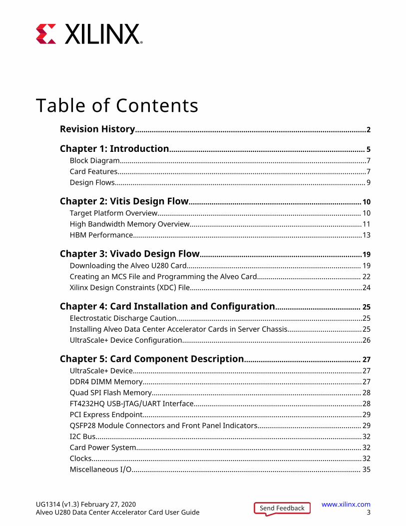
Table of ContentsRevision History...............................................................................................................2
Chapter 1: Introduction.............................................................................................. 5Block Diagram..............................................................................................................................7Card Features...............................................................................................................................7Design Flows................................................................................................................................ 9
Chapter 2: Vitis Design Flow................................................................................... 10Target Platform Overview........................................................................................................ 10High Bandwidth Memory Overview........................................................................................11HBM Performance.....................................................................................................................13
Chapter 3: Vivado Design Flow..............................................................................19Downloading the Alveo U280 Card......................................................................................... 19Creating an MCS File and Programming the Alveo Card..................................................... 22Xilinx Design Constraints (XDC) File........................................................................................24
Chapter 4: Card Installation and Configuration......................................... 25Electrostatic Discharge Caution...............................................................................................25Installing Alveo Data Center Accelerator Cards in Server Chassis......................................25UltraScale+ Device Configuration............................................................................................26
Chapter 5: Card Component Description........................................................ 27UltraScale+ Device.....................................................................................................................27DDR4 DIMM Memory................................................................................................................27Quad SPI Flash Memory........................................................................................................... 28FT4232HQ USB-JTAG/UART Interface......................................................................................28PCI Express Endpoint................................................................................................................29QSFP28 Module Connectors and Front Panel Indicators..................................................... 29I2C Bus........................................................................................................................................32Card Power System................................................................................................................... 32Clocks..........................................................................................................................................32Miscellaneous I/O..................................................................................................................... 35
UG1314 (v1.3) February 27, 2020 www.xilinx.comAlveo U280 Data Center Accelerator Card User Guide 3Send Feedback

Chapter 6: Known Issues and Limitations...................................................... 37
Appendix A: Regulatory and Compliance Information........................... 38CE Directives.............................................................................................................................. 38CE Standards..............................................................................................................................38Compliance Markings............................................................................................................... 39
Appendix B: Additional Resources and Legal Notices............................. 40Xilinx Resources.........................................................................................................................40Documentation Navigator and Design Hubs.........................................................................40References..................................................................................................................................40Please Read: Important Legal Notices................................................................................... 42
UG1314 (v1.3) February 27, 2020 www.xilinx.comAlveo U280 Data Center Accelerator Card User Guide 4Send Feedback

Chapter 1
IntroductionThe Xilinx® Alveo™ U280 Data Center accelerator cards are Peripheral Component Interconnectexpress (PCIe®) Gen3 x16 compliant and Gen4 x8 compatible cards featuring the Xilinx 16 nmUltraScale+™ technology. The Alveo U280 card offers 8 GB of HBM2 at 460 GB/s bandwidth toprovide high-performance, adaptable acceleration for memory-bound, compute-intensiveapplications including database, analytics, and machine learning inference.
The Alveo U280 Data Center accelerator cards are available in passive and active coolingconfigurations. Except where noted, this user guide applies to both the active and passiveversions of the U280 card. The following figure shows a passively cooled Alveo U280 acceleratorcard.
Figure 1: Alveo U280 Data Center Accelerator Card (Passive Cooling)
UG1314 (v1.3) February 27, 2020 www.xilinx.comAlveo U280 Data Center Accelerator Card User Guide 5Send Feedback

CAUTION! The Alveo U280 accelerator card with passive cooling is designed to be installed into a data centerserver, where controlled air flow provides direct cooling. Due to the card enclosure, switches and LEDs are notaccessible or visible. The card details in this user guide are provided to aid understanding of the card features. Ifthe cooling enclosure is removed from the card and the card is powered-up, external fan cooling airflow MUSTbe applied to prevent over-temperature shut-down and possible damage to the card electronics. Removing thecooling enclosure voids the board warranty.
See Appendix B: Additional Resources and Legal Notices for references to documents, files, andresources relevant to the Alveo U280 accelerator cards.
Chapter 1: Introduction
UG1314 (v1.3) February 27, 2020 www.xilinx.comAlveo U280 Data Center Accelerator Card User Guide 6Send Feedback

Block DiagramThe block diagram of the Alveo U280 accelerator card is shown in the following figure.
Figure 2: U280 Block Diagram
DDR4 DIMM
TEMPSENSOR
USBConn.
VCCINTRegulatorI2C
SPI2
SPI1
TEMPSENSOR
Temp.Sensor
EEPROM
I/OExpander
FanController
I2CMUX
GTY
I2C_SYSMON
4xG
TY
SI570DDR4 DIMM
UART
SYS_JTAG_ENEXT_JTAG_EN
UART UART
USB-TO-UART/JTAG
XCU280H2892
Satellite ControllerMSP432P4111
PCIe Edge Connector (X16)
SP1x4
CSn
QSFP0
I2CMUX
GTY
QSFP1 SMBU
S
12V_PEX
12V_AUX
JTAG
JTAG over GPIO
I2C
SPI WP
I/OExpander
I/OExpander
DDR42x72 bit
lmon
lmon
I2C_MAIN
GPIO
I2C
X22401-021120
Card FeaturesThe Alveo U280 accelerator card features are listed in this section. Detailed information for eachfeature is provided in Chapter 5: Card Component Description.
Chapter 1: Introduction
UG1314 (v1.3) February 27, 2020 www.xilinx.comAlveo U280 Data Center Accelerator Card User Guide 7Send Feedback
• Alveo U280 accelerator card:
○ XCU280 UltraScale+ device
• Memory (two independent dual-rank DDR4 interfaces)
○ 32 gigabyte (GB) DDR4 memory
○ 2x DDR4 16 GB, 2400 mega-transfers per second (MT/s), 64-bit with error correcting code(ECC) DIMM
○ x4/x8 unregistered dual inline memory module (UDIMM) support
• Configuration options
○ 1 gigabit (Gb) Quad Serial Peripheral Interface (SPI) flash memory
○ Micro-AB universal serial bus (USB) JTAG configuration port
• 16-lane PCI Express
• Two QSFP28 connectors
• USB-to-UART FT4232HQ bridge with Micro-AB USB connector
• PCIe Integrated Endpoint block connectivity
○ Gen1, 2, or 3 up to x16
○ Gen4 x8
• I2C bus
• Status LEDs
• Power management with system management bus (SMBus) voltage, current, and temperaturemonitoring
• Dynamic power sourcing based on external power supplied
• 65W PCIe slot functional with PCIe slot power only
• 150 W PCIe slot functional with PCIe slot power and 6-pin PCIe AUX power cable connected
• 225 W PCIe slot functional with PCIe slot power and 8-pin PCIe AUX power cable connected
• Onboard reprogrammable flash configuration memory
• JTAG and universal asynchronous receiver-transmitter (UART) access through the USB port
• UltraScale+ device configurable over USB/JTAG and Quad SPI configuration flash memory
Chapter 1: Introduction
UG1314 (v1.3) February 27, 2020 www.xilinx.comAlveo U280 Data Center Accelerator Card User Guide 8Send Feedback

Design FlowsThe preferred optimal design flow for targeting the Alveo Data Center accelerator card uses theVitis™ unified software platform. However, traditional design flows, such as RTL or HLx are alsosupported using the Vivado® Design Suite tools. The following figure shows a summary of thedesign flows.
Figure 3: Alveo Data Center Accelerator Card Design Flows
High complexity
Slowest
High
Simplicity
Time to Market
Hardware Expertise Required
Complexity abstracted
Fastest
Low
RTL Flow HLx Flow (IP integrator)
Traditional Flows
Target Platform
Vitis
X22272-020419
Requirements for the different design flows are listed in the following table.
Table 1: Requirements to Get Started with Alveo Data Center Accelerator Card DesignFlows
RTL Flow HLx Flow VitisFlow documentation UG9491 UG8952 UG14163
Hardware documentation UG1314 UG1314 N/A
Vivado tools support Board support XDC Board support XDC N/A
Programming the FPGA Vivado Hardware Manager Vivado Hardware Manager UG13014
Notes:1. UltraFast Design Methodology Guide for the Vivado Design Suite (UG949).2. Vivado Design Suite User Guide: System-Level Design Entry (UG895). See “Using the Vivado Design Suite Platform Board
Flow” in Chapter 2 and Appendix A.3. Vitis Accelerated Flow in the Vitis Unified Software Platform Documentation (UG1416).4. Getting Started with Alveo Data Center Accelerator Cards (UG1301).
Chapter 1: Introduction
UG1314 (v1.3) February 27, 2020 www.xilinx.comAlveo U280 Data Center Accelerator Card User Guide 9Send Feedback

Chapter 2
Vitis Design FlowThe following section is aimed at designers, and is intended as a quick start guide to the U280target platform. It describes how to link a kernel into the target platform and then run this kernelin hardware on the platform. Background information on the structure of the platform is alsoprovided.
For more details on the Vitis™ and hardware platforms, refer to the Vitis Accelerated Flow in theVitis Unified Software Platform Documentation (UG1416) and Embedded Processor PlatformDevelopment in the Vitis Unified Software Platform Documentation (UG1416).
Target Platform OverviewThe target platform consists of a Vivado® IP integrator block design with all of the required boardinterfaces configured and connected to the device I/Os.
The Vitis environment platforms require the device to remain up and running on a remote hostwhile applications are downloaded to it. Vitis target platforms use partial reconfiguration (PR)technology to enable compiled binary downloads to the accelerator device while the deviceremains online and linked to the PCIe® bus of the host. There is a fixed static logic partition thatcontains the board interface logic. The static partition is not reimplemented when the Vitisapplications are run. This is known as a target platform because it describes the boundary of thephysical board with the kernel logic. The target platform is intended to keep the device alive andto control reconfiguration and debugging of the device.
The dynamically programmable region defines the programmable device logic partition thatintegrates the user kernels from the Vitis environment. It contains memories, memory interfaces,and AXI interconnect logic. This logic is dynamically configured and implemented along with theVitis kernel logic each time an application is run. Each time a kernel application is run, partialreconfiguration technology is applied to reconfigure the dynamic region.
The dynamically programmable region has several DDR/HBM/PLRAM memory interfacescoupled with interconnect logic. The term PLRAM refers to internal UltraRAM/block RAM thatcan be accessed by host and user kernels. The dynamically programmable region uses theMemory Subsystem (MSS) IP (for DDR/PLRAM) and the HBM Memory Subsystem (HMSS) IP (forHBM). These subsystems are unique to the Vitis platforms. They contain multiple memoryinterfaces, coupled with the appropriate interconnect IP. When the dynamic region is being built
Chapter 2: Vitis Design Flow
UG1314 (v1.3) February 27, 2020 www.xilinx.comAlveo U280 Data Center Accelerator Card User Guide 10Send Feedback

(that is, when kernels are applied and connected to memory resources), the IP automatically trimaway any of the unused DDR/PLRAM interfaces and disable the unused HBM interfaces whichreside in the dynamic region. This allows for more of the device to be available for kernel logic,and reduces run time. Dynamic memory enablement is also optimal for power, because unusedmemories consume minimal power.
See Alveo Data Center Accelerator Card Platforms User Guide (UG1120) for information onavailable target platforms and resources.
High Bandwidth Memory OverviewU280 High Bandwidth Memory (HBM) devices incorporate 4 GB HBM stacks. Using stackedsilicon interconnect technology, the programmable logic communicates to the HBM stacksthrough memory controllers. The U280 has access to two stacks of 4 GB HBM, each consistingof 16 pseudo channels with direct access to 256 MB. A high-level diagram of the two HBMstacks is shown below.
The programmable logic has 32 HBM AXI interfaces. HBM AXI interfaces can access any memorylocation in any of the 32 HBM PCs on either of the HBM stacks through a built-in switchproviding access to the full 8 GB memory space. For more detailed information on the HBM,refer to AXI High Bandwidth Controller LogiCORE IP Product Guide (PG276). The flexible connectionbetween the programmable logic and the HBM stacks results in easy floorplanning and timingclosure as well as offering flexibility for kernel implementation.
Figure 4: High-Level Diagram of Two HBM Stacks0
4:4 4:4 4:4 4:4 4:4 4:4 4:4 4:4
MC0 MC1 MC2 MC3 MC4 MC5 MC6 MC7 MC8 MC9 MC10 MC11 MC12 MC13 MC14 MC15
PC00
PC01
PC02
PC03
PC04
PC05
PC06
PC07
PC08
PC09
PC10
PC11
PC12
PC13
PC14
PC15
PC16
PC17
PC18
PC19
PC20
PC21
PC22
PC23
PC24
PC25
PC26
PC27
PC28
PC29
PC30
PC31
HBM Stack 1 HBM Stack 2
SwitchNetwork
MCs, PHYs, etc.
1 2 3 4 5 6 7 8 9 10 11 12 13 14 15 16 17 18 19 20 21 22 23 24 25 26 27 28 29 30 31
X23418-102219
In addition to HBM, two Memory IP instances enable access to on-board DDR4 SDRAM. TheU280 accelerator card contains two channels of DDR4-2400 SDRAM, at 16 GB per channel for atotal of 40 GB global memory between internal HBM and external DDR4.
Chapter 2: Vitis Design Flow
UG1314 (v1.3) February 27, 2020 www.xilinx.comAlveo U280 Data Center Accelerator Card User Guide 11Send Feedback
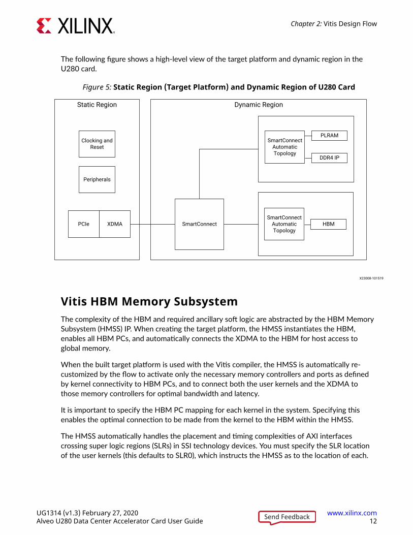
The following figure shows a high-level view of the target platform and dynamic region in theU280 card.
Figure 5: Static Region (Target Platform) and Dynamic Region of U280 Card
Static Region
Clocking and Reset
Peripherals
PCIe XDMA
Text
Text
SmartConnect Automatic Topology
PLRAM
DDR4 IP
SmartConnect Automatic Topology
HBMSmartConnect
Dynamic Region
X23008-101519
Vitis HBM Memory SubsystemThe complexity of the HBM and required ancillary soft logic are abstracted by the HBM MemorySubsystem (HMSS) IP. When creating the target platform, the HMSS instantiates the HBM,enables all HBM PCs, and automatically connects the XDMA to the HBM for host access toglobal memory.
When the built target platform is used with the Vitis compiler, the HMSS is automatically re-customized by the flow to activate only the necessary memory controllers and ports as definedby kernel connectivity to HBM PCs, and to connect both the user kernels and the XDMA tothose memory controllers for optimal bandwidth and latency.
It is important to specify the HBM PC mapping for each kernel in the system. Specifying thisenables the optimal connection to be made from the kernel to the HBM within the HMSS.
The HMSS automatically handles the placement and timing complexities of AXI interfacescrossing super logic regions (SLRs) in SSI technology devices. You must specify the SLR locationof the user kernels (this defaults to SLR0), which instructs the HMSS as to the location of each.
Chapter 2: Vitis Design Flow
UG1314 (v1.3) February 27, 2020 www.xilinx.comAlveo U280 Data Center Accelerator Card User Guide 12Send Feedback

The HBM subsystem in U280 devices performs well in applications where sequential data accessis required. However, for applications requiring random data access, performance can varysignificantly depending on the application requirements (for example, the ratio of read and writeoperations, minimum transaction size, and size of the memory space being addressed). TheRandom Access Memory Attachment (RAMA) IP helps to address such problems by significantlyimproving memory access efficiency in cases where the required memory exceeds 256 MB (oneHBM pseudo channel). Refer to RAMA LogiCORE IP Product Guide (PG310) for more information.
For using the RAMA IP to be considered, a kernel master should meet the following criteria:
• The master randomly accesses locations across more than one 256 MB HBM PC.
• The master uses a static, single ID on the AXI transaction ID ports (AxID), or the master usesslowly changing (pseudo-static) AXI transaction IDs.
If these conditions are not met, the thread creation used in the RAMA IP to improve performancehas little effect, and consumes programmable logic for no purpose.
Memory SubsystemWhen creating the target platform, the Memory Subsystem (MSS) instantiates all available DDR4memory controllers and automatically constructs an optimized SmartConnect-based network toconnect the XDMA to the memory controllers (two memory controllers in the case of the U280card) for host access to global memory. PLRAM memory (internal SRAM – UltraRAM and blockRAM) can also be accessed and is also created coupled to a similar optimal switch network.
When the built target platform is used with the Vitis compiler, the MSS is automatically re-customized by the flow to instantiate only the necessary memory as defined by kernelconnectivity to memory resources, and to automatically construct an optimized SmartConnect-based network to connect both the user kernels and the XDMA to those memory resources.Unmapped memory resources are not instantiated, and the SmartConnect network is optimizedaccordingly.
The MSS automatically handles the placement and timing complexities of AXI interfaces crossingSLRs in SSI technology devices, in the event that user kernels in a given SLR are mapped to oneor more memory controllers in a different SLR. Accordingly, you must specify the DDR/PLRAMresource requirements for each kernel in the system.
HBM PerformanceThe unique feature of the U280 platform is the hardened HBM subsystem, which is encapsulatedby the Vitis HBM Memory Subsystem (HMSS). Important performance figures,recommendations, and limitations are covered in this section.
Chapter 2: Vitis Design Flow
UG1314 (v1.3) February 27, 2020 www.xilinx.comAlveo U280 Data Center Accelerator Card User Guide 13Send Feedback

Performance FiguresA summary of the most common and least complex use case performances is shown below:
• Linear access point-to-point: single kernel master per HBM PC.
• Small random accesses point-to-point: single kernel master per HBM PC.
For linear accesses, the efficiency for all transaction sizes (read-only and write-only transactiontypes) is 91% when the transaction size is larger than 32 bytes.
Table 2: Linear Accesses (Single Kernel Master per HBM PC Performance)
TransactionSize Type Bandwidth1 Efficiency Total Bandwidth2
64 B+ WO 13.1 91% 419
64 B+ RO 13.1 91% 419
32 B WO 4.5 32% 144
32 B RO 4.5 31% 144
Notes:1. One master (GB/s).2. 32 masters (GB/s).
The achievable bandwidth (read-only and write-only) for small random accesses is shown below.
Table 3: Small Random Accesses (Single Kernel Master per HBM PC performance)
TransactionSize Type Bandwidth1 Efficiency Total Bandwidth2
64 B WO 4.9 32% 147
64 B RO 5.6 35% 160
32 B WO 4.5 31% 144
32 B RO 4.4 31% 141
Notes:1. One master (GB/s).2. 32 masters (GB/s).
Note: Because of the complexity and flexibility of the switch, there are many combinations that result incongestion at a particular memory location or in the switch itself. It is important to plan memory accessesso that kernels access limited memory where possible, and to isolate the memory accesses for differentkernels into different HBM PCs.
Interleaved read and write transactions cause a drop in efficiency with respect to read-only or write-onlydue to memory controller timing parameters (bus turnaround). The exact performance drop is dictated bythe read/write ratio and timing.
Chapter 2: Vitis Design Flow
UG1314 (v1.3) February 27, 2020 www.xilinx.comAlveo U280 Data Center Accelerator Card User Guide 14Send Feedback

Performance LimitationsThere is a bottleneck when a write transaction passes from HBM Stack 1 to HBM Stack 2. Thisbottleneck has the following effects:
• 33% of expected performance for 32B write transactions.
• 66% of expected performance for 64B write transactions.
• Other transaction sizes are not affected.
• Read transactions are not affected.
When planning memory resources, kernel masters planning to write at sizes of 32B/64B shouldnot access HBM memory resources on both stacks.
Figure 6: Write Bottleneck for Small Transactions
0
4:4 4:4 4:4 4:4 4:4 4:4 4:4 4:4
MC0 MC1 MC2 MC3 MC4 MC5 MC6 MC7 MC8 MC9 MC10 MC11 MC12 MC13 MC14 MC15
PC00
PC01
PC02
PC03
PC04
PC05
PC06
PC07
PC08
PC09
PC10
PC11
PC12
PC13
PC14
PC15
PC16
PC17
PC18
PC19
PC20
PC21
PC22
PC23
PC24
PC25
PC26
PC27
PC28
PC29
PC30
PC31
HBM Stack 1 HBM Stack 2
SwitchNetwork
MCs, PHYs, etc.
1 2 3 4 5 6 7 8 9 10 11 12 13 14 15 16 17 18 19 20 21 22 23 24 25 26 27 28 29 30 31
Write Bottleneck
X23423-102319
Performance NotesThe following should be noted with respect to the platform:
• The host is connected to one of the HBM ports on the platform.
○ Up to 32 kernel masters can access HBM.
○ The HBM switch provides for 32 masters to be connected. The host therefore shares aswitch port with one of the 32 kernel masters if required (this might not be optimal).
○ Xilinx recommends that no more than 31 kernel ports should be used if host and kernelinterference is expected to cause a problem.
• A kernel requiring access to HBM and DDR4 must use separate masters.
Chapter 2: Vitis Design Flow
UG1314 (v1.3) February 27, 2020 www.xilinx.comAlveo U280 Data Center Accelerator Card User Guide 15Send Feedback

○ This is a platform simplification.
○ DDR4/PLRAM access can be shared on a single master.
• A kernel master should only access a contiguous subset of the 32 HBM pseudo channels.
○ This makes optimization of the HBM connection point more straightforward.
• By default, without user memory planning (--connectivity.sp option on v++), all kernelmasters access a single HBM PC.
• By default, all kernels are assumed in SLR0.
○ This might lead to device congestion for complex designs, leading to a need for kernelfloorplanning.
RecommendationsRecommendations to get best performance from the platform are as follows:
• Select the kernel master data width and kernel frequency to match the followingrequirements:
○ The hardened HBM core clock runs at 450 MHz.
○ The hardened HBM AXI ports are 256 bits wide.
○ For linear transactions, the kernel should be configured to match the following bandwidth:
- 256 bits at 450 MHz (this might be a challenging design).
- 512 bits at 225 MHz (a larger but less challenging design).
○ It might be possible to achieve the same bandwidth with lower kernel frequency/bus widthcombinations. This depends on the traffic profile/switch usage.
○ For random transactions, it might be possible to scale the kernel master bandwidth down; akernel clock of 300 MHz and a width of 256 bits, for example. This must be assessed on acase-by-case basis.
• Use only HBM memory resources where possible.
○ DDR interfaces consume a large number of resources in the middle of SLR0 and SLR1, andmight in some cases cause congestion when routing to the HBM.
○ PLRAM resources also consume resources, but are more flexible in placement and aretherefore preferable to DDR if HBM is not sufficient.
• The platform offers a large amount of flexibility in terms of memory access patterns.
○ Measure memory subsystem performance to validate assumptions when not using simpleaccess (single master to single memory resource).
• Use as many HBM PCs as possible in parallel.
Chapter 2: Vitis Design Flow
UG1314 (v1.3) February 27, 2020 www.xilinx.comAlveo U280 Data Center Accelerator Card User Guide 16Send Feedback
○ High bandwidth can only be achieved with many kernel ports and many HBM PCs beingused in parallel.
• A kernel master should be capable of at least 64 outstanding read transactions and 32outstanding write transactions for random access.
○ More than this might add some performance at the expense of increased logic (up to 128outstanding transactions supported).
• Smaller transactions offer less efficiency than larger transactions. Use large transactionswhere possible.
• Avoid routing small write transactions across the boundary between HBM stacks 1 and 2.
○ When using 32B or 64B write transactions, ensure that a kernel accesses HBM[0:15] (stack1) or HBM[16:31] (stack 2); not both.
PLRAM Use and ModificationThe U280 platform contains HBM DRAM and DDR DRAM memory resources. An additionalmemory resource in the platform is internal FPGA SRAM (UltraRAM and block RAM). Theplatform initially contains six instances of 128 KB of PLRAM (block RAM). There are two PLRAMinstances in each SLR. The size and type (UltraRAM/block RAM) of each PLRAM can be changedbefore kernels are inserted. A pre-system-linkage Tcl file is used to change the PLRAM. Usage ofthe pre-system-linkage Tcl file can be enabled as follows on the v++ command line:
v++ --xp param:compiler.userPreSysLinkTcl=<full_path_to>/pre_user_tcl_file.tcl
An API is provided to change attributes of the PLRAM instance or memory resource:
sdx_memory_subsystem::update_plram_specification <memory_subsystem_bdcell> <plram_resource_name> <plram_specification>
In this API, <plram_specification> is a Tcl dictionary consisting of the following entries(entries below are the defaulted values for each instance in the platform):
{ SIZE 128K # Up to 4M AXI_DATA_WIDTH 512 # Up to 512 SLR_ASSIGNMENT SLR0 # SLR0 / SLR1 / SLR2 MEMORY_PRIMITIVE BRAM # BRAM or URAM READ_LATENCY 1 # To optimise timing path }
Chapter 2: Vitis Design Flow
UG1314 (v1.3) February 27, 2020 www.xilinx.comAlveo U280 Data Center Accelerator Card User Guide 17Send Feedback
In the example below, PLRAM_MEM00 is changed to be 2 MB in size and composed of UltraRAM;PLRAM_MEM01 is changed to be 4 MB in size and composed of UltraRAM. These resourcescorrespond to the v++ command line memory resources PLRAM[0:1].
# Setup PLRAM sdx_memory_subsystem::update_plram_specification [get_bd_cells /memory_subsystem] PLRAM_MEM00 { SIZE 2M AXI_DATA_WIDTH 512 SLR_ASSIGNMENT SLR0 READ_LATENCY 10 MEMORY_PRIMITIVE URAM}
sdx_memory_subsystem::update_plram_specification [get_bd_cells /memory_subsystem] PLRAM_MEM01 { SIZE 4M AXI_DATA_WIDTH 512 SLR_ASSIGNMENT SLR0 READ_LATENCY 10 MEMORY_PRIMITIVE URAM}
validate_bd_design -forcesave_bd_design
The READ_LATENCY is an important attribute, because it sets the number of pipeline stagesbetween memories cascaded in depth. This varies by design, and affects the timing QoR of theplatform and the eventual kernel clock rate. In the example above for PLRAM_MEM01(PLRAM[1]):
• 4 MB of memory are required in total.
• Each UltraRAM is 32 KB (64 bits wide). 4 MB × 32 KB → 128 UltraRAMs in total.
• Each PLRAM instance is 512 bits wide → 8 UltraRAMs are required in width.
• 128 total UltraRAMs with 8 UltraRAMs in width → 16 UltraRAMs in depth.
• A good rule of thumb is to pick a read latency of depth/2 + 2 → in this case, READ_LATENCY= 10.
This allows a pipeline on every second UltraRAM, resulting in the following:
• Good timing performance between UltraRAMs.
• Placement flexibility; not all UltraRAMs need to be placed in the same UltraRAM column forcascade.
Chapter 2: Vitis Design Flow
UG1314 (v1.3) February 27, 2020 www.xilinx.comAlveo U280 Data Center Accelerator Card User Guide 18Send Feedback

Chapter 3
Vivado Design FlowThis section provides a starting point for expert HDL developers using the RTL flows, ordevelopers who want to customize in HLx beyond the standard support in the Vivado® tools.
Downloading the Alveo U280 CardFor either the RTL or HLx flow, designers can start by downloading the U280 accelerator cardfiles (zip).
1. In Vivado, select Create New Project → RTL Project to open the New Project dialog box.
2. Click Update Board Repositories for the latest board files, and then select the U280 card:
UG1314 (v1.3) February 27, 2020 www.xilinx.comAlveo U280 Data Center Accelerator Card User Guide 19Send Feedback

The New Project Summary dialog box appears.
Chapter 3: Vivado Design Flow
UG1314 (v1.3) February 27, 2020 www.xilinx.comAlveo U280 Data Center Accelerator Card User Guide 20Send Feedback

3. Click Finish.
The Project Summary Overview page appears. You can now create the RTL-based project.
Chapter 3: Vivado Design Flow
UG1314 (v1.3) February 27, 2020 www.xilinx.comAlveo U280 Data Center Accelerator Card User Guide 21Send Feedback

Creating an MCS File and Programming theAlveo Card
For custom RTL flow, this section outlines the procedures to do the following:
• Create an MCS file (PROM image)
• Flash programming through the USB-JTAG (Micro-USB) interface
Create an MCS File (PROM Image)
The Alveo accelerator card contains a Quad SPI configuration flash memory part that can beconfigured over USB-JTAG. This part contains a protected region, with the factory base image atthe 0x00000000 address space. This base image points to the customer programmable region ata 0x01002000 address space offset.
To ensure that the PROM image is successfully loaded onto the Alveo accelerator card at poweron, the starting address must be set to 0x01002000 and the interface set to spix4 whencreating the MCS file. Details on adding this to the MCS file can be found in the UltraScaleArchitecture Configuration User Guide (UG570).
Chapter 3: Vivado Design Flow
UG1314 (v1.3) February 27, 2020 www.xilinx.comAlveo U280 Data Center Accelerator Card User Guide 22Send Feedback

In addition, the following code must be placed in the project XDC file to correctly configure theMCS file.
# Bitstream Configuration# ------------------------------------------------------------------------set_property CONFIG_VOLTAGE 1.8 [current_design]set_property BITSTREAM.CONFIG.CONFIGFALLBACK Enable [current_design]set_property BITSTREAM.GENERAL.COMPRESS TRUE [current_design]set_property CONFIG_MODE SPIx4 [current_design]set_property BITSTREAM.CONFIG.SPI_BUSWIDTH 4 [current_design]set_property BITSTREAM.CONFIG.CONFIGRATE 85.0 [current_design]set_property BITSTREAM.CONFIG.EXTMASTERCCLK_EN disable [current_design]set_property BITSTREAM.CONFIG.SPI_FALL_EDGE YES [current_design]set_property BITSTREAM.CONFIG.UNUSEDPIN Pullup [current_design]set_property BITSTREAM.CONFIG.SPI_32BIT_ADDR Yes [current_design]# ------------------------------------------------------------------------
After the XDC file has been updated, generate the MCS file with the following command(including the quotation marks.)
write_cfgmem -force -format mcs -interface spix4 -size 1024 -loadbit "up 0x01002000 <input_file.bit>" -file "<output_file.mcs>"
Where:
• <input_file.bit> is the filename of the input .bit file
• <output_file.mcs> is the MCS output filename
Program the Alveo Card
After the MCS file is created, see the procedure in the "Programming the FPGA Device" chapterin the Vivado Design Suite User Guide: Programming and Debugging (UG908) to connect to theAlveo Data Center accelerator card using the hardware manager.
1. Select Add Configuration Device and select the mt25qu01g-spi-x1_x2_x4 part.
2. Right-click the target to select Program the Configuration Memory Device.
a. Select the MCS file target.
b. Select Configuration File Only.
c. Click OK.
3. After programming has completed, disconnect the card in the hardware manager, anddisconnect the USB cable from the Alveo accelerator card.
4. Perform a cold reboot on the host machine to complete the card update.
IMPORTANT! If you are switching between an Alveo Data Center accelerator card target platform and acustom design, revert the card to the golden image before loading an alternate image into the PROM. SeeGetting Started with Alveo Data Center Accelerator Cards (UG1301) for more information.
Chapter 3: Vivado Design Flow
UG1314 (v1.3) February 27, 2020 www.xilinx.comAlveo U280 Data Center Accelerator Card User Guide 23Send Feedback

Xilinx Design Constraints (XDC) FileRTL users can reference the Vivado Design Suite User Guide: Using Constraints (UG903) for moreinformation. The Alveo accelerator card XDC files are available for download from theirrespective websites along with this user guide.
Chapter 3: Vivado Design Flow
UG1314 (v1.3) February 27, 2020 www.xilinx.comAlveo U280 Data Center Accelerator Card User Guide 24Send Feedback

Chapter 4
Card Installation and Configuration
Electrostatic Discharge CautionCAUTION! ESD can damage electronic components when they are improperly handled, and can result in totalor intermittent failures. Always follow ESD-prevention procedures when removing and replacing components.
To prevent ESD damage:
• Use an ESD wrist or ankle strap and ensure that it makes skin contact. Connect the equipmentend of the strap to an unpainted metal surface on the chassis.
• Avoid touching the adapter against your clothing. The wrist strap protects components fromESD on the body only.
• Handle the adapter by its bracket or edges only. Avoid touching the printed circuit board orthe connectors.
• Put the adapter down only on an antistatic surface such as the bag supplied in your kit.
• If you are returning the adapter to Xilinx Product Support, place it back in its antistatic bagimmediately.
Installing Alveo Data Center AcceleratorCards in Server Chassis
Because each server or PC vendor's hardware is different, for physical board installationguidance, see the manufacturer’s PCI Express® board installation instructions.
For programming and start-up details, see Getting Started with Alveo Data Center Accelerator Cards(UG1301).
UG1314 (v1.3) February 27, 2020 www.xilinx.comAlveo U280 Data Center Accelerator Card User Guide 25Send Feedback

UltraScale+ Device ConfigurationThe Alveo U280 accelerator card supports two UltraScale+™ FPGA configuration modes:
• Quad SPI flash memory
• JTAG using USB JTAG configuration port
The FPGA bank 0 mode pins are hardwired to M[2:0] = 001 master SPI mode with pull-up/downresistors.
At power up, the FPGA is configured by the Quad SPI NOR flash device (MicronMT25QU01GBBA8E12-0SIT) with the FPGA_CCLK operating at a clock rate up to 105 MHzusing the master serial configuration mode. The Quad SPI flash memory NOR device has acapacity of 1 Gb.
If the JTAG cable is plugged in, QSPI configuration might not occur. JTAG mode is alwaysavailable independent of the mode pin settings.
For complete details on configuring the FPGA, see the UltraScale Architecture Configuration UserGuide (UG570).
Table 4: Configuration Modes
Configuration Mode M[2:0] Bus Width CCLK DirectionMaster SPI 001 x1, x2, x4 FPGA output
JTAG Not applicable – JTAG overrides x1 Not applicable
Chapter 4: Card Installation and Configuration
UG1314 (v1.3) February 27, 2020 www.xilinx.comAlveo U280 Data Center Accelerator Card User Guide 26Send Feedback

Chapter 5
Card Component DescriptionThis chapter provides a functional description of the components of the Alveo™ U280 DataCenter accelerator card.
UltraScale+ DeviceThe Alveo U280 accelerator card is populated with the 16 nm UltraScale+™ XCU280 FPGA. Thisdevice incorporates two 4 GB High Bandwidth Memory (HBM) stacks adjacent to the device die.Using SSI technology, the device communicates to the HBM stacks through memory controllersthat connect through the silicon interposer at the bottom of the device. Each XCU280 FPGAcontains two 4 GB HBM stacks, resulting in up to 8 GB of HBM per device. The device includes32 HBM AXI interfaces used to communicate with the HBM. The flexible addressing feature thatis provided by a built-in switch allows for any of the 32 HBM AXI interfaces to access anymemory address on either one or both of the HBM stacks. This flexible connection between thedevice and the HBM stacks is helpful for floorplanning and timing closure.
Related InformationKnown Issues and Limitations
DDR4 DIMM MemoryTwo independent dual-rank DDR4 interfaces are available. The card is populated with twosocketed single-rank Micron MTA18ASF2G72PZ-2G3B1IG 16 GB DDR4 RDIMMs. Each DDR4DIMM is 72 bits wide (64 bits plus support for ECC). The DDR4 and HBM interfaces have a100.000 MHz system reference clock input. The 100.000 MHz reference clock to bank 65 ofSLR0 is used by both the HBM and the DDR4 C0 interface in banks 64, 65, and 66. The C1DDR4 interface is located in banks 68, 69, and 70 with the 100.000 MHz system clock going intobank 69 of SLR1. Banks 64, 65, 66, 68, 69, and 70 are powered from an onboard 1.2V regulator.
The detailed FPGA and DIMM pin connections for the feature described in this section aredocumented in the Alveo U280 accelerator card XDC file.
UG1314 (v1.3) February 27, 2020 www.xilinx.comAlveo U280 Data Center Accelerator Card User Guide 27Send Feedback
For more details about the Micron DDR4 DIMM, see the Micron MTA18ASF2G72PZ-2G3B1IGdata sheet at the Micron website: http://www.micron.com.
Related InformationXilinx Design Constraints (XDC) File
Quad SPI Flash MemoryThe Quad SPI device provides 1 Gb of nonvolatile storage.
• Part number: MT25QU01GBBB8E12-0AAT (Micron)
• Supply voltage: 1.8V
• Datapath width: 4 bits
• Data rate: 100 MHz
For more flash memory details, see the Micron MT25QU01GBBB8E12-0AAT data sheet at theMicron website.
For configuration details, see the UltraScale Architecture Configuration User Guide (UG570). Thedetailed FPGA and Flash pin connections for the feature described in this section aredocumented in the Alveo U280 accelerator card XDC file, referenced in Xilinx Design Constraints(XDC) File.
Related InformationXilinx Design Constraints (XDC) File
FT4232HQ USB-JTAG/UART InterfaceThe USB connector for debug and development is located on the rear of the card and requires amicro-AB USB connection cable. The USB is connected to a FTDI FT4232HQ device, which hasthe following connectivity:
• ADBUS → JTAG connection to the UltraScale+ device JTAG through a level shifter that can bedisabled by the satellite controller to prevent user tampering.
Note: This port is also connected to the satellite controller through a level shifter that can be disabledby the satellite controller to prevent user tampering.
• ACBUS → RS232 serial port connection to the satellite controller.
○ Port connection needs to be configured for no parity, 8 data bits, 1 stop bit with a line rateof 115200.
Chapter 5: Card Component Description
UG1314 (v1.3) February 27, 2020 www.xilinx.comAlveo U280 Data Center Accelerator Card User Guide 28Send Feedback

• ABBUS → RS232 serial port connection to the UltraScale+ device.
○ Port connection needs to be configured by user and UltraScale+ device design.
○ USB_UART_TX connects to IO_L24N_T3U_N11_75 (pin A28) on the UltraScale+ device.
○ USB_UART_RX connects to IO_T3U_N12_75 (pin B33) on the UltraScale+ device.
The FTDI FT4232HQ data sheet is available on the FTDI website: https://www.ftdichip.com/.
PCI Express EndpointThe Alveo U280 accelerator card implements a 16-lane PCI Express® edge connector thatperforms data transfers at the rate of 2.5 giga-transfers per second (GT/s) for Gen1, 5.0 GT/s forGen2, 8.0 GT/s for Gen3 applications, and 16.0 GT/s for Gen4 applications.
The detailed UltraScale+ device and PCIe pin connections for the feature described in thissection are documented in the accelerator card design constraints (XDC) file. The endpoint iscompliant to the v3.0 specification, and compatible with the specification (specifications areavailable here). For additional information on Gen4 compatible features, see UltraScale+ DevicesIntegrated Block for PCI Express LogiCORE IP Product Guide (PG213).
Related InformationXilinx Design Constraints (XDC) File
QSFP28 Module Connectors and Front PanelIndicators
The Alveo accelerator cards host two 4-lane small form-factor pluggable (QSFP) connectors thataccept an array of optical modules and copper cables. Each connector is housed within a singleQSFP cage assembly.
The QSFP+ connectors sideband control signals (MODSELL, RESETL, MODPRSL, INTL, andLPMODE) are behind an I2C expander and are not accessible from the UltraScale+ device. TheQSFP+ I2C interface and sideband control signals on the Alveo U280 accelerator card are onlyaccessible through the satellite controller, and are currently not supported with the exceptionthat the satellite controller does actively drive the LPMODE signal low so that an optical moduleis enabled when inserted. The MODSELL, RESETL, MODPRSL, INTL, and LPMODE sidebandsignals are defined in the small form factor (SFF) specifications listed below.
The components visible through the card PCIe panel/bracket top to bottom are:
Chapter 5: Card Component Description
UG1314 (v1.3) February 27, 2020 www.xilinx.comAlveo U280 Data Center Accelerator Card User Guide 29Send Feedback

• Done, power bad, and 2x status LEDs
○ Currently, the two status LEDs (green and yellow) are undefined and have no currentfunctionality.
○ The done LED is blue and indicates that the UltraScale+ device is configured.
○ The power bad LED is red and indicates there is not a power good situation. This signal isderived from the AND'ing of all the power supplies power good signals on the card andinverting the result.
• QSFP0: the QSFP0 interface is the upper QSFP connector and has the high-speedconnections to the UltraScale+ device listed in the following table.
Table 5: QSFP0 Interface High-Speed Connections
Signal Name Bank Pin Reference Pin NumberMGT_SI570_CLOCK0_C_N 134 MGTREFCLK0N_134 T43
MGT_SI570_CLOCK0_C_P 134 MGTREFCLK0P_134 T42
QSFP0_CLOCK_N 134 MGTREFCLK1N_134 R41
QSFP0_CLOCK_P 134 MGTREFCLK1P_134 R40
QSFP0_RX1_N 134 MGTYRXN0_134 L54
QSFP0_RX2_N 134 MGTYRXN1_134 K52
QSFP0_RX3_N 134 MGTYRXN2_134 J54
QSFP0_RX4_N 134 MGTYRXN3_134 H52
QSFP0_RX1_P 134 MGTYRXP0_134 L53
QSFP0_RX2_P 134 MGTYRXP1_134 K51
QSFP0_RX3_P 134 MGTYRXP2_134 J53
QSFP0_RX4_P 134 MGTYRXP3_134 H51
QSFP0_TX1_N 134 MGTYTXN0_134 L49
QSFP0_TX2_N 134 MGTYTXN1_134 L45
QSFP0_TX3_N 134 MGTYTXN2_134 K47
QSFP0_TX4_N 134 MGTYTXN3_134 J49
QSFP0_TX1_P 134 MGTYTXP0_134 L48
QSFP0_TX2_P 134 MGTYTXP1_134 L44
QSFP0_TX3_P 134 MGTYTXP2_134 K46
QSFP0_TX4_P 134 MGTYTXP3_134 J48
• QSFP1: the QSFP1 interface is the lower QSFP connector and has the high-speedconnections to the UltraScale+ device listed in the following table.
Table 6: QSFP1 Interface High-Speed Connections
Signal Name Bank Pin Reference Pin NumberMGT_SI570_CLOCK1_C_N 135 MGTREFCLK0N_135 P43
MGT_SI570_CLOCK1_C_P 135 MGTREFCLK0P_135 P42
Chapter 5: Card Component Description
UG1314 (v1.3) February 27, 2020 www.xilinx.comAlveo U280 Data Center Accelerator Card User Guide 30Send Feedback

Table 6: QSFP1 Interface High-Speed Connections (cont'd)
Signal Name Bank Pin Reference Pin NumberQSFP1_CLOCK_N 135 MGTREFCLK1N_135 M43
QSFP1_CLOCK_P 135 MGTREFCLK1P_135 M42
QSFP1_RX1_N 135 MGTYRXN0_135 G54
QSFP1_RX2_N 135 MGTYRXN1_135 F52
QSFP1_RX3_N 135 MGTYRXN2_135 E54
QSFP1_RX4_N 135 MGTYRXN3_135 D52
QSFP1_RX1_P 135 MGTYRXP0_135 G53
QSFP1_RX2_P 135 MGTYRXP1_135 F51
QSFP1_RX3_P 135 MGTYRXP2_135 E53
QSFP1_RX4_P 135 MGTYRXP3_135 D51
QSFP1_TX1_N 135 MGTYTXN0_135 G49
QSFP1_TX2_N 135 MGTYTXN1_135 E49
QSFP1_TX3_N 135 MGTYTXN2_135 C49
QSFP1_TX4_N 135 MGTYTXN3_135 A50
QSFP1_TX1_P 135 MGTYTXP0_135 G48
QSFP1_TX2_P 135 MGTYTXP1_135 E48
QSFP1_TX3_P 135 MGTYTXP2_135 C48
QSFP1_TX4_P 135 MGTYTXP3_135 A49
For additional information about the quad SFF pluggable (28 Gb/s QSFP+) module, see theSFF-8663 and SFF-8679 specifications for the 28 Gb/s QSFP+ at the SNIA Technology Affiliateswebsite: https://www.snia.org/sff/specifications2.
Each QSFP connector has its own clock generator with two selectable frequencies of161.132812 MHz or 156.2500 MHz. See Clocks for details on the QSFP+ clocking.
The detailed UltraScale+ device and QSFP pin connections for the feature described in thissection are documented in the Xilinx Design Constraints (XDC) File.
Related InformationXilinx Design Constraints (XDC) File
Chapter 5: Card Component Description
UG1314 (v1.3) February 27, 2020 www.xilinx.comAlveo U280 Data Center Accelerator Card User Guide 31Send Feedback

I2C BusThe Alveo U280 accelerator cards implement an I2C bus network to communicate withnumerous sensors and voltage regulators on the card. These I2C interfaces are not accessiblefrom the UltraScale+ device and are only accessible via the satellite controller. For moreinformation on accessing various sensors on the card via the UltraScale+ device, see CardManagement Solution Subsystem Product Guide (PG348) for card management system access andimplementation (the device tree details are available in the board support package).
Card Power SystemLimited power system telemetry is available through the card management system (CMS) I2C IP.See Card Management Solution Subsystem Product Guide (PG348) for information on how the I2CIP is instantiated during the UltraScale+ device design process that begins after the Alveo DataCenter accelerator card is selected from the Vivado Design Suite Boards tab. See Design Flowsfor more information.
ClocksThe Alveo U280 card has reference and system clocks located in multiple banks to support themany features on the card.
• System clocks: the UltraScale+ device system reference clocks are supplied by a local 100.000MHz Abracon AB-557-03-HCHC-F-L-C-T oscillator and also connected to a Silicon LabsSI53340-B-GM 1:4 clock buffer. The local oscillator clock is distributed to bank 65 (DDR4),bank 69 (HBM and DDR4), and bank 75 (common logic).
○ SI53340-B-GM → OUT0 SYSCLK0_P/SYSCLK0_N 100.000 MHz. System clock for firstDDR4 MIG interface and HBM memories.
- Pins: IO_L12P_T1U_N10_GC_A08_D24_65/IO_L12N_T1U_N11_GC_A09_D25_65.
○ SI53340-B-GM → OUT1 SYSCLK1_P/SYSCLK1_N 100.000 MHz. System clock for secondDDR4 MIG interface.
- Pins: IO_L13P_T2L_N0_GC_QBC_69/IO_L13N_T2L_N1_GC_QBC_69.
○ SI53340-B-GM → OUT3 SYSCLK3_P/SYSCLK3_N 100.000 MHz - bank 75 100 MHz inputclock.
- Pins: IO_L11P_T1U_N8_GC_75/IO_L11N_T1U_N9_GC_75.
Chapter 5: Card Component Description
UG1314 (v1.3) February 27, 2020 www.xilinx.comAlveo U280 Data Center Accelerator Card User Guide 32Send Feedback

The U280 card has several reference input clocks to support PCIe x16 and bifurcated PCIe x8.
• The PCIe edge connector to the 100 MHz clock source is buffered through a Silicon LabsSI53322-B-GM 1:2 clock buffer and supplied to bank 225 and 227 for the PCIe GTYtransceivers.
○ PCIe fingers PEX_REFCLK_P/PEX_REFCLK_P 100.000 MHz is buffered through a SiliconLabs SI53322-B-GM 1:2 clock buffer and distributed to these pins:
- OUT0 → PCIE_CLK0_P/PCIE_CLK0_N 100.000 MHz - PCIe REFCLK0 for bifurcated x8lanes 0-7 synchronous clocking.
- Pins: MGTREFCLK0P_227_AL15/MGTREFCLK0N_227_AL14.
- OUT1 → PCIE_CLK1_P/PCIE_CLK1_N 100.000 MHz - PCIe REFCLK0 for x16 andbifurcated x8 lanes 8-15 synchronous clocking.
- Pins: MGTREFCLK0P_225_AR15/MGTREFCLK0N_225_AR14.
• An onboard Abracon AB-557-03-HCHC-F-L-C-T @ 100.000 MHz dual output PCIe MEMsoscillator is also used with a Silicon Labs SI53340-B-GM 1-to-4 clock buffer to supply clockingto the PCIe interfaces on bank 224 through bank 227.
○ SI53340-B-GM → OUT2 SYSCLK2_P/SYSCLK2_N 100.000 MHz - PCIe REFCLK1 forbifurcated x8 lanes 0-7 asynchronous clocking.
- Pins: MGTREFCLK1P_227_AK13/MGTREFCLK1N_227_AK12.
○ AB-557-03 OUT0 → SYS_CLK5_P/SYS_CLK5_N @ 100.000 MHz - PCIe REFCLK1 for x16and bifurcated x8 lanes 8-15 asynchronous clocking.
- Pins: MGTREFCLK1P_225_AP13/MGTREFCLK1N_225_AP12.
Each QSFP quad has both reference clocks connected as follows:
• QSFP0 clock MGTREFCLK1:
○ Clock generator: Silicon Labs 546BAB001028BBG.
○ Output CLK_P/N: the QSFP0_CLOCK_P/N clock is an AC-coupled LVDS 156.25 MHz clockwired to the GTY bank 134 MGTREFCLK1clock input pins (MGTREFCLK1P_134_R40/MGTREFCLK1N_134_R41).
○ Clock controls:
- OE_B ← Active-Low input to SI546 to enable output frequency.
Pin: "QSFP0_OEB" - IO_L9P_T1L_N4_AD12P_75_H32.
- FS ← Clock select pin .
FS = 1 → 161.132812 MHz 1.8V LVDS (default when FPGA pin Hi-Z or driven High).
FS = 0 → 156.25 MHz 1.8V LVDS when driven low by FPGA.
Pin: "QSFP0_FS" - IO_L9N_T1L_N5_AD12N_75_G32.
Chapter 5: Card Component Description
UG1314 (v1.3) February 27, 2020 www.xilinx.comAlveo U280 Data Center Accelerator Card User Guide 33Send Feedback

• QSFP1 clock MGTREFCLK1.
○ Clock generator: Silicon Labs 546BAB001028BBG.
○ Output CLK_P/N: the QSFP0_CLOCK_P/N clock is an AC-coupled LVDS 156.25 MHz clockwired to the GTY bank 135 MGTREFCLK1clock input pins (MGTREFCLK1P_135_M42/MGTREFCLK1N_135_M43).
○ Clock controls:
- OE_B ← Active-Low input to SI546 to enable output frequency.
Pin: "QSFP1_OEB" - IO_L8N_T1L_N3_AD5N_75_H30.
- FS ← Clock select pin.
FS = 1 → 161.132812 MHz 1.8V LVDS (default when FPGA pin Hi-Z or driven High).
FS = 0 → 156.25 MHz 1.8V LVDS when driven low by FPGA.
Pin: "QSFP1_FS" - IO_L7N_T1L_N1_QBC_AD13N_75_G33.
• QSFP0/1 clock MGTREFCLK0.
○ Clock generator: SI570 - SiLabs 570BAB000544DG at 156.250 MHz programmableoscillator
Reprogramming I2C access only possible via the satellite controller through an I2Cmultiplexer. There is no access to the Si570 I2C interface from the FPGA. The output ofthe SI570 device is fed into a Silicon Labs SI53340-B-GM 1:4 LVDS clock buffer anddistributed to the FPGA MGTREFCLK0 of banks 134 and 135. In addition, a third clock isdistributed to bank 75.
○ SI53340-B-GM outputs:
- OUT0: USER_SI570_CLOCK_P/USER_SI570_CLOCK_N 156.250 MHz - general purposesystem clock.
Pins: IO_L12P_T1U_N10_GC_75_G30/IO_L12N_T1U_N11_GC_75_F30.
- OUT1: Not connected.
Pins: N/A
- OUT2 MGT_SI570_CLOCK0_C_P/MGT_SI570_CLOCK0_C_N 156.250 MHz - QSFP0REFCLK0.
Pins: MGTREFCLK0P_134_T42/MGTREFCLK0N_134_T43.
- OUT3 MGT_SI570_CLOCK1_C_P/MGT_SI570_CLOCK1_C_N 156.250 MHz - QSFP0REFCLK1.
Pins: MGTREFCLK0P_135_P42/MGTREFCLK0N_135_P43.
Chapter 5: Card Component Description
UG1314 (v1.3) February 27, 2020 www.xilinx.comAlveo U280 Data Center Accelerator Card User Guide 34Send Feedback

In summary, the UltraScale+ device reference clocks are supplied by a local 100.000 MHzAbracon AB-557-03-HCHC-F-L-C-T oscillator also connected to a Silicon Labs SI53340-B-GM1:4 clock buffer and the PCIe edge connector 100 MHz clock source. The local oscillator clock isdistributed to bank 65, bank 69, bank 75, bank 225, and bank 227 for the DDR4, common logicand PCIe GTY transceivers. The PCIe edge connector 100 MHz clock source is buffered througha Silicon Labs SI53322-B-GM 1:2 clock buffer and supplied to bank 225 and bank 227 for thePCIe GTY transceivers. The detailed FPGA and clock pin connections for the feature described inthis section are documented in the U280 accelerator card XDC file.
Related InformationXilinx Design Constraints (XDC) File
Miscellaneous I/OOn the U280 card, the UltraScale+ device has a single bank with various inputs and outputs tocommunicate with the satellite controller and other devices on the card. See the XDC file for allof the signal connections. This section only references the signals that are usable in bank 75.Bank 75 is powered from a 1.8V source.
IMPORTANT! The D32 pin must be connected appropriately or tied to logic 0. If D32 is pulled up, floated, ortied to 1, the U280 card might become unrecoverable after programming.
Table 7: Bank 75 SLR2 Miscellaneous I/O Descriptions
Signal Name Direction Pin I/O DescriptionFPGA_RXD_MSP Input E28 IO_L18P_T2U_N10_AD2P_75 Satellite controller CMS UART
receive (115200, no parity, 8 bits, 1stop bit).
FPGA_TXD_MSP Output D29 IO_L18N_T2U_N11_AD2N_75 Satellite controller CMS UARTtransmit (115200, no parity, 8 bits, 1stop bit).
I2C_FPGA_SDA Bi Dir C33 IO_T2U_N12_75 Slave I2C data connection fromsatellite controller to FPGA.
I2C_FPGA_SCL Bi Dir C30 IO_L19P_T3L_N0_DBC_AD9P_75 Slave I2C clock connection fromsatellite controller to FPGA.
I2C_MAIN_INT_B Output B31 IO_L19N_T3L_N1_DBC_AD9N_75 Slave I2C active-Low systeminterrupt output from FPGA tosatellite controller.
I2C_MUX0_INTB_FPGA Input D31 IO_L16N_T2U_N7_QBC_AD3N_75 Slave I2C active-Low interruptoutput from FPGA to satellitecontroller.
PEX_PWRBRKN Input C32 IO_L17N_T2U_N9_AD10N_75 PEX_PWRBRKN active-Low inputfrom PCIe connector signaling PCIecard to shut down card power inserver failing condition.
Chapter 5: Card Component Description
UG1314 (v1.3) February 27, 2020 www.xilinx.comAlveo U280 Data Center Accelerator Card User Guide 35Send Feedback
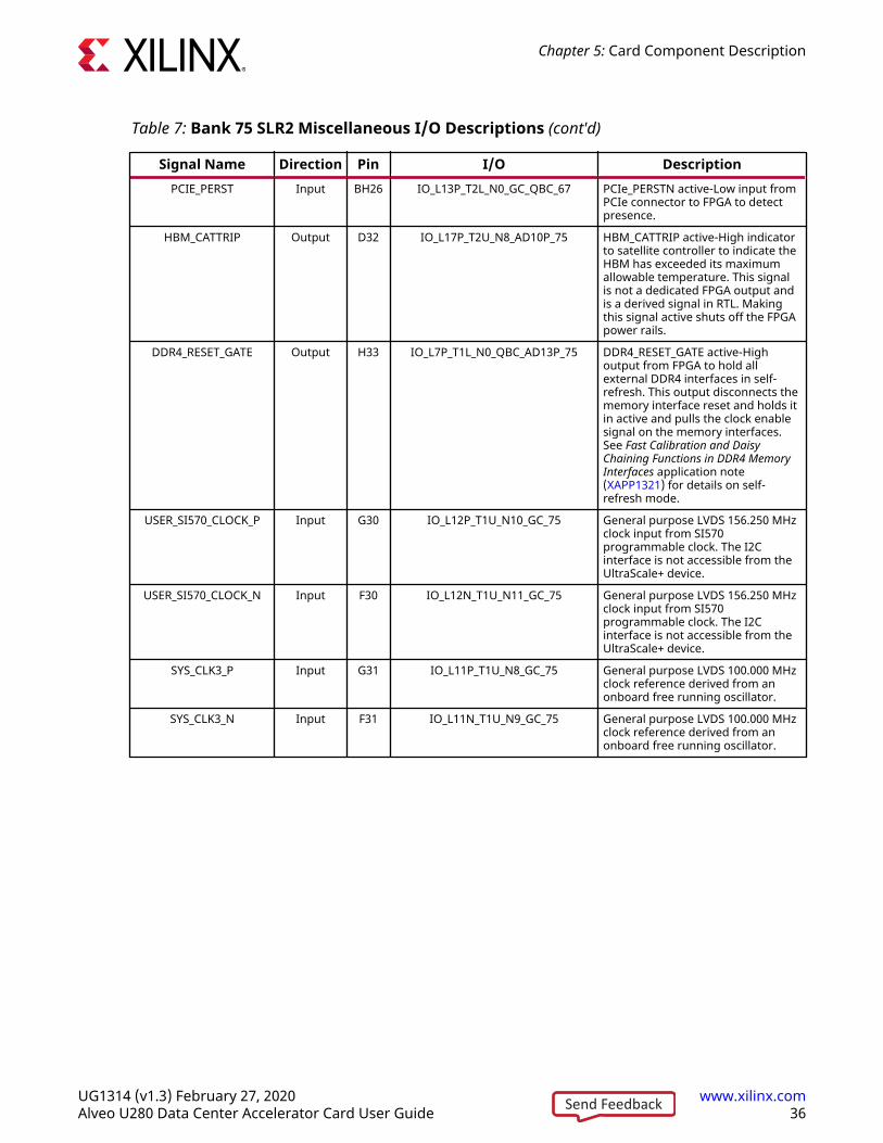
Table 7: Bank 75 SLR2 Miscellaneous I/O Descriptions (cont'd)
Signal Name Direction Pin I/O DescriptionPCIE_PERST Input BH26 IO_L13P_T2L_N0_GC_QBC_67 PCIe_PERSTN active-Low input from
PCIe connector to FPGA to detectpresence.
HBM_CATTRIP Output D32 IO_L17P_T2U_N8_AD10P_75 HBM_CATTRIP active-High indicatorto satellite controller to indicate theHBM has exceeded its maximumallowable temperature. This signalis not a dedicated FPGA output andis a derived signal in RTL. Makingthis signal active shuts off the FPGApower rails.
DDR4_RESET_GATE Output H33 IO_L7P_T1L_N0_QBC_AD13P_75 DDR4_RESET_GATE active-Highoutput from FPGA to hold allexternal DDR4 interfaces in self-refresh. This output disconnects thememory interface reset and holds itin active and pulls the clock enablesignal on the memory interfaces.See Fast Calibration and DaisyChaining Functions in DDR4 MemoryInterfaces application note(XAPP1321) for details on self-refresh mode.
USER_SI570_CLOCK_P Input G30 IO_L12P_T1U_N10_GC_75 General purpose LVDS 156.250 MHzclock input from SI570programmable clock. The I2Cinterface is not accessible from theUltraScale+ device.
USER_SI570_CLOCK_N Input F30 IO_L12N_T1U_N11_GC_75 General purpose LVDS 156.250 MHzclock input from SI570programmable clock. The I2Cinterface is not accessible from theUltraScale+ device.
SYS_CLK3_P Input G31 IO_L11P_T1U_N8_GC_75 General purpose LVDS 100.000 MHzclock reference derived from anonboard free running oscillator.
SYS_CLK3_N Input F31 IO_L11N_T1U_N9_GC_75 General purpose LVDS 100.000 MHzclock reference derived from anonboard free running oscillator.
Chapter 5: Card Component Description
UG1314 (v1.3) February 27, 2020 www.xilinx.comAlveo U280 Data Center Accelerator Card User Guide 36Send Feedback

Chapter 6
Known Issues and LimitationsAR 71752 is the master answer record for the Alveo Data Center accelerator cards. For TechnicalSupport, open a Support Service Request.
UG1314 (v1.3) February 27, 2020 www.xilinx.comAlveo U280 Data Center Accelerator Card User Guide 37Send Feedback
Appendix A
Regulatory and ComplianceInformation
This product is designed and tested to conform to the European Union directives and standardsdescribed in this section.
CE Directives2014/35/EC, Low Voltage Directive (LVD)
2014/30/EC, Electromagnetic Compatibility (EMC) Directive
CE StandardsEN standards are maintained by the European Committee for Electrotechnical Standardization(CENELEC). IEC standards are maintained by the International Electrotechnical Commission (IEC).
Electromagnetic CompatibilityEN:55032:2015, Information Technology Equipment Radio Disturbance Characteristics – Limits andMethods of Measurement
EN:55024:2015, Information Technology Equipment Immunity Characteristics – Limits and Methodsof Measurement
This is a Class A product. In a domestic environment, this product can cause radio interference, inwhich case the user might be required to take adequate measures.
SafetyIEC 60950-1, 2nd Edition, 2014, Information technology equipment – Safety, Part 1: Generalrequirements
Appendix A: Regulatory and Compliance Information
UG1314 (v1.3) February 27, 2020 www.xilinx.comAlveo U280 Data Center Accelerator Card User Guide 38Send Feedback

EN 60950-1, 2nd Edition, 2014, Information technology equipment – Safety, Part 1: Generalrequirements
Compliance MarkingsIn August of 2005, the European Union (EU) implemented the EU Waste Electricaland Electronic Equipment (WEEE) Directive 2002/96/EC and later the WEEE RecastDirective 2012/19/EU. These directives require Producers of electronic andelectrical equipment (EEE) to manage and finance the collection, reuse, recyclingand to appropriately treat WEEE that the Producer places on the EU market afterAugust 13, 2005. The goal of this directive is to minimize the volume of electricaland electronic waste disposal and to encourage re-use and recycling at the endof life.Xilinx has met its national obligations to the EU WEEE Directive by registering inthose countries to which Xilinx is an importer. Xilinx has also elected to join WEEECompliance Schemes in some countries to help manage customer returns atend-of-life.If you have purchased Xilinx-branded electrical or electronic products in the EUand are intending to discard these products at the end of their useful life, pleasedo not dispose of them with your other household or municipal waste. Xilinx haslabeled its branded electronic products with the WEEE Symbol to alert ourcustomers that products bearing this label should not be disposed of in a landfillor with municipal or household waste in the EU.
This product complies with Directive 2002/95/EC on the restriction of hazardoussubstances (RoHS) in electrical and electronic equipment.
This product complies with CE Directives 2006/95/EC, Low Voltage Directive (LVD)and 2004/108/EC, Electromagnetic Compatibility (EMC) Directive.
Appendix A: Regulatory and Compliance Information
UG1314 (v1.3) February 27, 2020 www.xilinx.comAlveo U280 Data Center Accelerator Card User Guide 39Send Feedback

Appendix B
Additional Resources and LegalNotices
Xilinx ResourcesFor support resources such as Answers, Documentation, Downloads, and Forums, see XilinxSupport.
Documentation Navigator and Design HubsXilinx® Documentation Navigator (DocNav) provides access to Xilinx documents, videos, andsupport resources, which you can filter and search to find information. To open DocNav:
• From the Vivado® IDE, select Help → Documentation and Tutorials.
• On Windows, select Start → All Programs → Xilinx Design Tools → DocNav.
• At the Linux command prompt, enter docnav.
Xilinx Design Hubs provide links to documentation organized by design tasks and other topics,which you can use to learn key concepts and address frequently asked questions. To access theDesign Hubs:
• In DocNav, click the Design Hubs View tab.
• On the Xilinx website, see the Design Hubs page.
Note: For more information on DocNav, see the Documentation Navigator page on the Xilinx website.
ReferencesThese documents provide supplemental material useful with this guide:
Appendix B: Additional Resources and Legal Notices
UG1314 (v1.3) February 27, 2020 www.xilinx.comAlveo U280 Data Center Accelerator Card User Guide 40Send Feedback
Product Websites
The most up-to-date information related to the Alveo™ U280 card and documentation isavailable on the Alveo U280 Data Center Accelerator Card.
Supplemental Documents
The following Xilinx document provide supplemental material useful with this guide.
• AXI High Bandwidth Controller LogiCORE IP Product Guide (PG276)
• UltraFast Design Methodology Guide for the Vivado Design Suite (UG949)
• Vivado Design Suite User Guide: System-Level Design Entry (UG895)
• Getting Started with Alveo Data Center Accelerator Cards (UG1301)
• UltraScale Architecture Configuration User Guide (UG570)
• Vivado Design Suite User Guide: Programming and Debugging (UG908)
• Virtex UltraScale+ FPGA Data Sheet: DC and AC Switching Characteristics (DS923)
• UltraScale Architecture-Based FPGAs Memory IP LogiCORE IP Product Guide (PG150)
• Vivado Design Suite User Guide: Using Constraints (UG903)
• UltraScale Architecture PCB Design User Guide (UG583)
Additional Links
The following links provide supplemental material useful with this guide.
• Xilinx, Inc: https://www.xilinx.com
• Micron Technology: http://www.micron.com
(MTA18ASF2G72PZ-2G3B1IG, MT25QU01GBB8E12-OAAT)
• Si53322 Data Sheet: https://www.silabs.com/documents/public/data-sheets/si5332x-datasheet.pdf
• AB-557-03 Data Sheet: https://abracon.com/Oscillators/AB-557-03.pdf
• Si546 Data Sheet: https://www.silabs.com/documents/public/data-sheets/si546-datasheet.pdf
• Future Technology Devices International, Ltd.: http://www.ftdichip.com
(FT4232HQ)
• QSFP+ module: https://members.snia.org/document/dl/25969
Appendix B: Additional Resources and Legal Notices
UG1314 (v1.3) February 27, 2020 www.xilinx.comAlveo U280 Data Center Accelerator Card User Guide 41Send Feedback

Please Read: Important Legal NoticesThe information disclosed to you hereunder (the "Materials") is provided solely for the selectionand use of Xilinx products. To the maximum extent permitted by applicable law: (1) Materials aremade available "AS IS" and with all faults, Xilinx hereby DISCLAIMS ALL WARRANTIES ANDCONDITIONS, EXPRESS, IMPLIED, OR STATUTORY, INCLUDING BUT NOT LIMITED TOWARRANTIES OF MERCHANTABILITY, NON-INFRINGEMENT, OR FITNESS FOR ANYPARTICULAR PURPOSE; and (2) Xilinx shall not be liable (whether in contract or tort, includingnegligence, or under any other theory of liability) for any loss or damage of any kind or naturerelated to, arising under, or in connection with, the Materials (including your use of theMaterials), including for any direct, indirect, special, incidental, or consequential loss or damage(including loss of data, profits, goodwill, or any type of loss or damage suffered as a result of anyaction brought by a third party) even if such damage or loss was reasonably foreseeable or Xilinxhad been advised of the possibility of the same. Xilinx assumes no obligation to correct anyerrors contained in the Materials or to notify you of updates to the Materials or to productspecifications. You may not reproduce, modify, distribute, or publicly display the Materialswithout prior written consent. Certain products are subject to the terms and conditions ofXilinx's limited warranty, please refer to Xilinx's Terms of Sale which can be viewed at https://www.xilinx.com/legal.htm#tos; IP cores may be subject to warranty and support terms containedin a license issued to you by Xilinx. Xilinx products are not designed or intended to be fail-safe orfor use in any application requiring fail-safe performance; you assume sole risk and liability foruse of Xilinx products in such critical applications, please refer to Xilinx's Terms of Sale which canbe viewed at https://www.xilinx.com/legal.htm#tos.
AUTOMOTIVE APPLICATIONS DISCLAIMER
AUTOMOTIVE PRODUCTS (IDENTIFIED AS "XA" IN THE PART NUMBER) ARE NOTWARRANTED FOR USE IN THE DEPLOYMENT OF AIRBAGS OR FOR USE IN APPLICATIONSTHAT AFFECT CONTROL OF A VEHICLE ("SAFETY APPLICATION") UNLESS THERE IS ASAFETY CONCEPT OR REDUNDANCY FEATURE CONSISTENT WITH THE ISO 26262AUTOMOTIVE SAFETY STANDARD ("SAFETY DESIGN"). CUSTOMER SHALL, PRIOR TO USINGOR DISTRIBUTING ANY SYSTEMS THAT INCORPORATE PRODUCTS, THOROUGHLY TESTSUCH SYSTEMS FOR SAFETY PURPOSES. USE OF PRODUCTS IN A SAFETY APPLICATIONWITHOUT A SAFETY DESIGN IS FULLY AT THE RISK OF CUSTOMER, SUBJECT ONLY TOAPPLICABLE LAWS AND REGULATIONS GOVERNING LIMITATIONS ON PRODUCTLIABILITY.
Appendix B: Additional Resources and Legal Notices
UG1314 (v1.3) February 27, 2020 www.xilinx.comAlveo U280 Data Center Accelerator Card User Guide 42Send Feedback
Copyright
© Copyright 2019-2020 Xilinx, Inc. Xilinx, the Xilinx logo, Alveo, Artix, Kintex, Spartan, Versal,Virtex, Vivado, Zynq, and other designated brands included herein are trademarks of Xilinx in theUnited States and other countries. OpenCL and the OpenCL logo are trademarks of Apple Inc.used by permission by Khronos. PCI, PCIe, and PCI Express are trademarks of PCI-SIG and usedunder license. AMBA, AMBA Designer, Arm, ARM1176JZ-S, CoreSight, Cortex, PrimeCell, Mali,and MPCore are trademarks of Arm Limited in the EU and other countries. All other trademarksare the property of their respective owners.
Appendix B: Additional Resources and Legal Notices
UG1314 (v1.3) February 27, 2020 www.xilinx.comAlveo U280 Data Center Accelerator Card User Guide 43Send Feedback


![When HLS Meets FPGA HBM: Benchmarking and Bandwidth … · 2020. 10. 14. · HBM channels and FPGA logic due to the power restriction [30]. Alveo U280 has a similar architecture as](https://static.fdocuments.us/doc/165x107/60b4a9a525821659e7622ed9/when-hls-meets-fpga-hbm-benchmarking-and-bandwidth-2020-10-14-hbm-channels.jpg)