Alternative Approaches to 3-Dimensional Packaging and ... · 3-Dimensional Packaging and...
29
Alternative Approaches to 3-Dimensional Packaging and Interconnection Joseph Fjelstad SiliconPipe, Inc. www.SiPipe.com IC Packaging … a Technology in Transition In the past, IC packaging has been considered a “formula-matic” activity Now, the importance of IC packaging has risen significantly IC package is commonly the limiting factor in chip/system performance Improved IC packaging options and design approach are required to meet future needs and overcome the limitations of current PCBs
Transcript of Alternative Approaches to 3-Dimensional Packaging and ... · 3-Dimensional Packaging and...

1
Alternative Approaches to 3-Dimensional Packaging and Interconnection
Joseph FjelstadSiliconPipe, Inc.www.SiPipe.com
IC Packaging … a Technology in Transition
In the past, IC packaging has been considered a “formula-matic” activity
Now, the importance of IC packaging has risen significantly
IC package is commonly the limiting factor in chip/system performance
Improved IC packaging options and design approach are required to meet future needs and overcome the limitations of current PCBs

2
Perspective
Modern Electronics are driven by IC packaging technology Thus far there have been three eras in packaging
Through hole – DIPs, PGAs
Surface mount – PQFPs, BGAs
Chip Scale – Flip Chip, Wafer Level
3D packaging is the dawn of the next era Seeds of 3D packaging were planted in the 1980’s
Package Selection Growth

3
3-Dimensional Drivers
Consumer demand is for smaller, lighter products with more features.
Portable products (e.g cell phones, PDAs, digital cameras etc.) require volumetric system miniaturization and interconnection (VSMI) to meet the demand for increased functionality in less overall space.
This is best achieved with 3D packaging technology.
Worldwide Mobile Phone Example

4
What is 3D Packaging?
Packaging and interconnection technologies that address and utilize all dimensions of space in their construction are embraced by the term 3D packaging.
There are several approaches to 3D packaging
Stacked chips in packages – ICs stacked and interconnected inside the package before encapsulation.
Stacked packages – packaged chips stacked one atop another
Hybrid stacked structures – Stacked chip or multi-chip packages that are themselves stacked.
Chips in separate packages separated in space but interconnected on multiple planes
Benefits of 3D Packaging3D packaging offers several benefits including:
Smaller, Thinner Packages – i.e. More silicon functions per cm3
Significant size and weight reductionsReduced Packaging Costs Reduction in TestReduction in Number of Components on AssemblyPackage I/O reductionReduced Time to Market More freedom is silicon design and mixing of technologies Simplified system level circuit routing to direct chip to chip interconnect. Reduction motherboard size and layer countReduced System Cost (SiP vs SoC) Higher performance at reduced power

5
Die Stacked StructuresMany potential solutions in die stacking.
Stacked face up and wire bonded Flip chip stacks Combination flip chip and wire bond
Stacked chip structures generally use thinned die (75µm- 200µm) Substrates are normally thin core rigid laminate or flexible substrates. Wire bonding technology modified to allow low loop wire bonding Reverse bonding technology provides solutionsOver mold material is thinner to keep height down multiple die within the package.
Stacked die technology
Source: Amkor

6
Chip Stacking Package Options
Stacked Package Structures
A few potential solutions for package stacking…Stacked lead frame packages
TSOPs, DIPs (not common)
Stacked Peripheral array packagesExamples: Micro Z®, etCSP®
Fold over full area array packagesTessera, Valtronics
Applications:Stacked DRAM memory
Stacked SRAM and flash
Others

7
Stacked Packaging Options
Stacked Lead Frame Packages
Stacked Packaging Options
Stacked Peripheral Array Packages

8
Stacked Package Comparison
Size comparison of stacked package technologies
Stacked TSOP µZ Package
TSOP
2-die
4-die
1-die
Source: Tessera
From PQFP
to StackBGA

9
Finished Structures
Folded Package Options
10
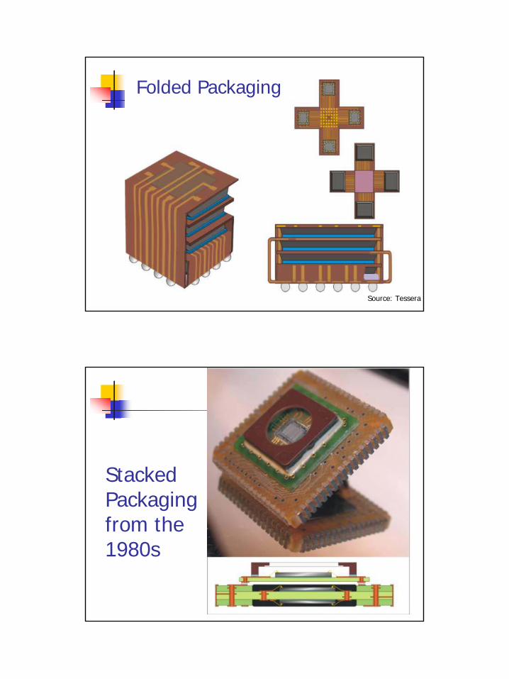
Source: Tessera
Folded Packaging
Stacked Packaging from the 1980s

11
3D for High Speed?
Technology Trends:
Digital electronics and telecom operating frequencies have entered into the multi-GHz range…
Currently, the mainstream SERDES data rate is 1.25Gb/s to 5Gb/s and is expected to reach 10Gb/s to 40Gb/s within the next 3-5 years.
The entire electronic networking and computer industry, (i.e. High Speed Backplanes, Fiber Channel, InfiniBand, OIF, RapidIO, 3GIO, and XAUI), are moving into multi-gigabit serial link topologies.
Intel P4, CPU frequency is currently 3GHz and could increase to 10GHz in three to five years.
12
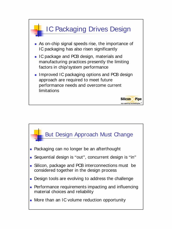
IC Packaging Drives Design
As on-chip signal speeds rise, the importance of IC packaging has also risen significantly
IC package and PCB design, materials and manufacturing practices presently the limiting factors in chip/system performance
Improved IC packaging options and PCB design approach are required to meet future performance needs and overcome current limitations
But Design Approach Must Change
Packaging can no longer be an afterthought
Sequential design is “out”, concurrent design is “in”
Silicon, package and PCB interconnections must be considered together in the design process
Design tools are evolving to address the challenge
Performance requirements impacting and influencing material choices and reliability
More than an IC volume reduction opportunity

13
IC Packaging Challenges/Needs
Chip, packaging & substrate co-designDigital & analog mixed signal, transient thermal analysis, thermo-mechanical analysis, electrical power disturb, signal integrity
Organic substratesTg, dielectric loss, planarity & warpage, processing temperature, (e.g Pb Free impact), moisture absorption
Electrostatic Discharge (ESD) control Need for better and alternative ESD control methods
Cu/low-k impact on IC packaging Wire bond, FC and underfill on Cu & low-k wafers (adhesion, material strength, etc.)
Understanding the Issues
High speed means rapid rise times
Rise time degradation is a major concern
Rise time degradation is caused by:
Signal loss
Conductor and dielectric loss
Impedance Discontinuities
Connectors, vias, material changes, mfg defects

14
Performance Limiters
PCB Problem Areas

15
Moving Ahead of Moore’s Law

16
The Interconnect Gap
There is a 10X gap between signal speeds on IC and signal speeds on PC boards. This gap is increasing and rapidly becoming a major technology bottleneck.
Traditional chip-based interconnect gap solutions are running out of steam. Problems with traditional copper solutions include signal loss, signal degradation, cross-talk, reflections, power requirements new channel-based solutions are needed.
Silicon and optical solutions are being readied but which is right?
Unleashing IC Performance

17
How Do You Get There ?
Chip or Channel?Chip choices…
Chip solutions use complex signaling technology and higher transmit power to move high-speed chip-to-chip signals over increasing complex PCBs.
Limitations on transistors available for I/O and insufficient power budgets prevents I/O design from solving fundamental channel problems.
The companies that address chip-to-chip speed issues do so by providing increasingly expensive semiconductor I/O designs requiring more sophisticated SERDES designs, highly engineered packages and increasing power requirements.
Channel choices…Optical solutions:
Challenges for optical: cost, power, heat, manufacturability, conversion cost and business disruption.
Copper solutions move chip-to-chip high speed signals through innovative copper alternatives to traditional PC boards.
Challenges in copper: new IC packaging techniques, high–speed, low power transceivers, new constant-impedance connectors, new ESD in-package techniques and PCB signal loss mitigation.
18
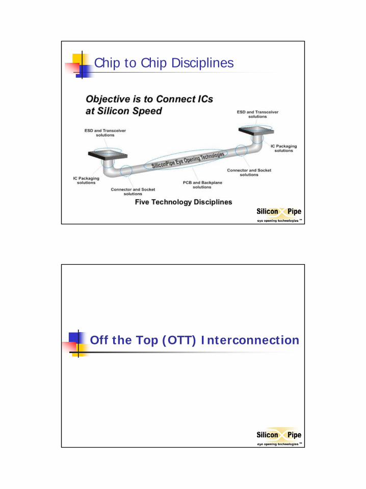
Chip to Chip Disciplines
Off the Top (OTT) Interconnection

19
20Gbps Chip-to-Chip Solution
Clearing the Channel
SiliconPipe, Inc - Copyright 2004 All rights reserved

20
Eye Diagram Comparison
SiliconPipe, Inc - Copyright 2004 All rights reserved
20Gbps Channel for Chip-to-ChipTechnological Advantages...
High speed flex based channel technology enables the link between packages over distances up to 15 inches, with near zero skew at speeds to 20Gbps per channel.
(15Gbps/channel packaging for 0.13µm CMOS structures, 20Gbps for 90nm CMOS structures)
Chip interconnections are standard in the package is structured as a commodity item allowing many companies to bid for the task
Easily standardized interconnection architecture
Applicable to various die sizes and performances
Increased design flexibility
Full compatibility with existing packaging assembly

21
Rethinking Circuit Design
Patents Pending
OTT Advantage at Test

22
Performance Potential
Example of a “Perfect Channel”

23
1Kb/s 10Kb/s 100Kb/s 1Mb/s 1Gb/s100Mb/s10Mb/s 1Tb/s100Gb/s10Gb/s 1000Tb/s100Tb/s10Tb/s
Phone Modems
CableModems 1Gig En DWDMEthernet
Fast Ethernet 10 Gig En
OC12 OC192 OC768DSL T1 OC3T3
Optical Performance - Copper Simplicity
ResearchProduction or in Development
Electron performance
Photonic performance
Production or in Development Research
Supercharged Copper
Interconnects
Can Copper Deliver the Promise?
24
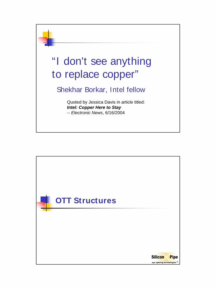
“I don't see anything to replace copper”
Shekhar Borkar, Intel fellow
Quoted by Jessica Davis in article titled: Intel: Copper Here to Stay-- Electronic News, 6/16/2004
OTT Structures

25
New I/O Placement
Off The Top IC Packaging

26
OTT Package (before chip placement)
Prototypes

27
Directly from Chip to Chip
Connector Option Example

28
Retrofitting Possibilities
Retrofitting Possibilities
29
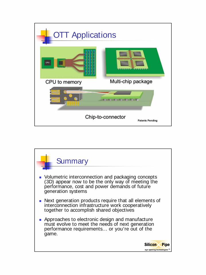
OTT Applications
Summary
Volumetric interconnection and packaging concepts (3D) appear now to be the only way of meeting the performance, cost and power demands of future generation systems
Next generation products require that all elements of interconnection infrastructure work cooperatively together to accomplish shared objectives
Approaches to electronic design and manufacture must evolve to meet the needs of next generation performance requirements… or you’re out of the game.