Alliance Memory-AS4C512M32MD3-15BCN€¦ · AS4C512M32MD3-15BCN Confidential -1 of 104 ... Table 1....
104
Alliance Memory Inc. 511 Taylor Way, San Carlos, CA 94070 TEL: (650) 610-6800 FAX: (650) 620-9211 Alliance Memory Inc. reserves the right to change products or specification without notice Revision History 16Gb AS4C512M32MD3-15BCN - 178 ball FBGA PACKAGE Revision Details Date Rev 1.0 Preliminary datasheet Nov. 2016 AS4C512M32MD3-15BCN Confidential - 1 of 104 - Rev.1.1 Aug. 2017 Aug. 2017 Rev 1.1 Pin Assignment revise
Transcript of Alliance Memory-AS4C512M32MD3-15BCN€¦ · AS4C512M32MD3-15BCN Confidential -1 of 104 ... Table 1....

AA
AS4C512M32MD3-15BCN
C
lliance Memory Inc. 511 Taylor Way, San Carlos, CA 94070 TEL: (650) 610-6800 FAX: (650) 620-9211 lliance Memory Inc. reserves the right to change products or specification without notice
Revision History 16Gb AS4C512M32MD3-15BCN - 178 ball FBGA PACKAGE
Revision Details Date Rev 1.0 Preliminary datasheet Nov. 2016
Aug. 2017Rev 1.1 Pin Assignment revise
onfidential - 1 of 104 - Rev.1.1 Aug. 2017

Spe- D- O
AS4C512M32MD3-15BCN
C
HIGH PERFORMANCE 16Gbit LPDDR3 SDRAM 8 BANKS X 32Mbit X 32 X 2 CS
cificationsensity : 16G bitsrganization :
- 32M words x 32 bits x 8 banks x 2 CSackage :
Features- Low power consumption- Eight-bit prefetch DDR architecture and BL8 only- Eight internal banks for concurrent operation- Double data rate architecture for command, address
- P- 178-ball FBGA- Lead-free (RoHS compliant) and Halogen-free
- Power supply :- VDD1 = 1.8V (1.7V~1.95V)- VDD2/VDDQ/VDDCA = 1.2V (1.14V~1.3V)
- HSUL_12 interface (High Speed Unterminated Logic1.2V)
- Data rate :- 1333Mbps RL=10
- RL / WL select setA / setB- Driver strength :
- Typical : 34.3/40/48/60/80 Ω- PD34.3_PU40 / PD40_PU48 / PD34.3_PU48
- ODT: RZQ/4, RZQ/2, RZQ/1 (RZQ = 240 Ω)- Operating case temperature range
- Commercial Tc = -25°C to +85°C
and data Bus- Bidirectional and differential data strobe per byte of
data (DQS and DQS)- DQS is edge-aligned with data for READs, center-
aligned with data for WRITEs- Differential clock inputs (CK and CK)- Data mask (DM) for write data- Programmable READ and WRITE latencies (RL/WL)- Auto Refresh and Self Refresh- Per-bank refresh for concurrent operation- Partial-array self refresh (PASR)- On-chip temperature sensor to control self refresh rate
for temperature compensated self refresh (TCSR)- Deep power-down mode (DPD)- Selectable output drive strength (DS)- Selectable On-Die Termination- CA Training- Write leveling via MR setting- Clock stop capability- DQ calibration offering specific DQ output patterns- ZQ calibration
Table1.OrderingInformation
Product part No Org Temperature Max Clock (MHz)
512M x 32 667
Package
178-ball FBGA
Table2.SpeedGradeInformationSpeed Grade Clock Frequency Read latency (RL) Write Latency (Set A) Clock Cycle Time (tCK)
AS4C512M32MD3-15BCN Commercial -25°C to +85°C
LPDDR3-1333 667 MHz 10 6 1.5
onfidential - 2 of 104 - Rev.1.1 Aug. 2017

16Gb LPDDR3 SDRAM Signals and Addressing
Configuration 512Mb x 32
CS CS0, CS1
CKE CKE0, CKE1
CK, CK CK, CK
DQ [31:0]
DQS / DM [3:0] / [3:0]
CA [9:0]
Bank Address BA0 ~ BA2
Row Address R0 ~ R13
Column Address C0 ~ C10
AS4C512M32MD3-15BCN
Confidential - 3 of 104 - Rev.1.1 Aug. 2017

Pin Assignment - 11.0mmX11.5mm 178B FBGA
<Top View>
Notes:1. Do Not Use (DNU)2. Top view, A1 in Top Left Corner
DQ16 DQ17 DQ18 DQ19
VDD1
DM0 VSSQ
DQ4 DQ5
VDDQ DQ1
DM2 DQ0
DQ20 DQ21
DQS0_t
DQS0_c
DQ6 DQ7
DQ2 DQ3
DQS2_t
DQS2_c
DQ22 DQ23
VSSQ DNU
DNU DNUVDD2 VDD2 VDDQ
CA0
DNU VSS VSS VSS VSSQ
DNU DNU
NC VSS VSSQ
VDD1 VDD1 VDD1 VDD1
VSS
VSS
VSSQ
LPDDR3
Commend/Address
LPDDR3 Data IO
Power
(VDD1,VDD2,VDDCA,
VDDQ,VREF)
Ground
(VSS,VSSCA,VSSQ)
CA6 VSS VSSQ VDDQ DQ14 DQ13 DQ12
VDDCA
VDDCA
VSS
CK_c
VSS
VDDCA
VDDCA
CA2
CA1
CA5
VSSCA
VDDCA
CK_t
CKE0
CS0_n
CA4
VSS VSSQ
VDD2 VSSQ
VDD2 VDD2
VDD2 VDD2
VDD2 VDD2
VDD2 VSS
VSS VSSQ
VSS VSSQ
VDD2 VDD2
DQ11 DQ10
DM1 VSSQ
VDDQ VDDQ
ODT VDDQ
VDDQ NC
DQ9 DQ8
DQS1_t
DQS1_c
VSSQ VDDQ
VDDQVref(DQ)
VSSQ VDDQ
CA3
VSSCA
DNU VSS
DNU DNU VDD1 DNU
DNU
DNU DNU
VSS
VSSCA
VSSCA
Vref(CA)
VSSCA
CKE1
CS1_n
VSSCA
VSS
VDD2
ZQ0 VSS VSSQ
CA9
CA8
CA7
VSSCA
VSSCA
VSS VSSQ
VDD2 VDD2
ZQ1
NC
VDD2
VDD1 VDD1VDD1 VDD2 VDD2 VDD1 VDDQ
DQ31 DQ30
DQ27 DQ26
DM3 DQ15
DQ29 DQ28
DQ25 DQ24
DQS3_t
DQS3_c
1 2 3 4 5 6 7 8 9 10 1311 12
A
B
C
D
E
F
G
H
J
K
L
M
N
P
R
T
U
A
B
C
D
E
F
G
H
J
K
L
M
N
P
R
T
U
1 2 3 4 5 6 7 8 9 10 1311 12
VDDQ
VSSQ
VDDQ
VSSQ
VDDQ
VDDQ
VSSQ
VDDQ
VDD2
VSS
VDD2
VDDQ
VSSQ
AS4C512M32MD3-15BCN
Confidential - 4 of 104 - Rev.1.1 Aug. 2017

Signal Pin Description
Pin Type Function
CK, CK(CK_t, CK_c)
Input Clock : CK and CK are differential clock inputs. All CA inputs are sampled on both rising and falling edges of CK. CS and CKE inputs are sampled at the rising edge of CK. AC timings are referenced to clock.
CKE Input Clock Enable : CKE HIGH activates and CKE LOW deactivates the internal clock signals, input buffers, and output drivers. Power-saving modes are entered and exited via CKE transitions. CKE is considered part of the command code. CKE is sampled at the rising edge of CK.
CS(CS_n) Input Chip Select : CS is considered part of the command code and is sampled at the rising edge of CK.
CA0~CA9 Input Command/address inputs: Provide the command and address inputs according to the command truth table.
DM0~DM3 Input Input Data Mask : DM is an input mask signal for write data. Although DM balls are input-only, the DM loading is designed to match that of DQ and DQS balls. DM[3:0] is DM for each of the four data bytes, respectively.
DQ0~DQ31 Input/output Data input/output: Bidirectional data bus.
DQS[3:0],(DQS_t[3:0]),
DQS[3:0](DQS_c[3:0])
Input/output Data strobe: The data strobe is bidirectional (used for read and write data) and complementary (DQS and DQS). It is edge-aligned output with read data and centered input with write data. DQS[3:0]/DQS[3:0] is DQS for each of the four data bytes, respectively
NC No Connect: No internal electrical connection is present.
ODT Input On-Die Termination: This signal enables and disables termination on the DRAM DQ bus according to the specified mode register setting.
ZQ Input External impedance (240 ohm): This signal is used to calibrate the device out-put impedance.
VDD1 Supply Core power: Supply 1.
VDD2 Supply Core power: Supply 2.
VDDQ Supply DQ power supply: Isolated on the die for improved noise immunity.
VDDCA Supply Command/address power supply: Command/address power supply.
VREF(DQ), VREF(CA)
Supply Reference voltage: VREF(CA) is reference for command/address input buffers,VREF(DQ) is refer-ence for DQ input buffers.
VSS Supply Common ground
VSSQ Supply DQ Common ground
VSSCA Supply CA Common ground
AS4C512M32MD3-15BCN
Confidential - 5 of 104 - Rev.1.1 Aug. 2017

Functional Block Diagram
512Mb X 32 178 Ball LPDDR3
Notes:1. Total current consumption is dependent to user operating conditions. AC and DC Characteristics shown in this specification are based on a single die.
CS0_n
4Gb x16 deviceCKE0
VDD1, VDD2, VDDCA,
(256M x 16)
CA0~CA9
DQ0~DQ15
CK_t, CK_c
ZQ0
VSS, VSSCA, VSSQ
4Gb x16 device(256M x 16)
VDDQ, Vref(CA/DQ)
DQ16~DQ31
ZQ1
4Gb x16 device(256M x 16)
4Gb x16 device(256M x 16)
CS1_nCKE1
DQS0_t~DQS1_t, DQS0_c~DQS1_cDM0~DM1
DQS2_t~DQS3_t, DQS2_c~DQS3_cDM2~DM3
ODT Ball
ODT GND
AS4C512M32MD3-15BCN
Confidential - 6 of 104 - Rev.1.1 Aug. 2017

Simplified State Diagram
Self
Idle1
Reading
Precharging
Writing
ACT
RD
SREF
REF
PD
MRR
PDX
PDX
PD
WR
Automatic Sequence
Command Sequence
RDAWRA
Refreshing
Refreshing
PowerDown
Active
withReading
with
Active
ReadingWriting
PR(A) = Precharge (All)
MRW = Mode Register Write
SREF = Enter Self Refresh
REF = Refresh
PD = Enter Power DownPDX = Exit Power Down
ACT = Activate
WR(A) = Write (with Autoprecharge)RD(A) = Read (with Autoprecharge)
SREFX
MR
AutoprechargeAutoprecharge
DeepPower DPDX PowerDownOn
MRR = Mode Register Read
SREFX = Exit Self RefreshDPD = Enter Deep Power DownDPDX = Exit Deep Power Down
MRR
MRW
DPD
PowerApplied
MRWriting2
MRReading
Resetting
MRReading
Reset
Reset = Reset is achieved through MRW command
MRR
RDA3WRA3
Reset
Resetting
Active
DownPower
Idle
Idle
PR, PRA
PowerDown
Resetting
PD
PDX
PR, PRA
RD3WR3
AS4C512M32MD3-15BCN
Confidential - 7 of 104 - Rev.1.1 Aug. 2017

AS4C512M32MD3-15BCN
C
Basic FunctionalityLPDDR3-SDRAM is a high-speed synchronous DRAM device internally configured as an 8-bank memory.
LPDDR3 devices use a double data rate architecture on the Command/Address (CA) bus to reduce the number of input pins in the system. The 10-bit CA bus contains command, address, and bank information. Each command uses one clock cycle, during which command information is transferred on both the positive and negative edge of the clock.
These devices also use a double data rate architecture on the DQ pins to achieve high speed operation. The double data rate architecture is essentially an 8n pre-fetch architecture with an interface designed to transfer two data bits per DQ every clock cycle at the I/O pins. A single read or write access for the LPDDR3 SDRAM effectively consists of a single 8n-bit wide, one clock cycle data transfer at the internal DRAM core and eight corresponding n-bit wide, one-half-clock-cycle data transfers at the I/O pins.
Read and write accesses to the LPDDR3 SDRAMs are burst oriented; accesses start at a selected location and continue for a programmed number of locations in a programmed sequence. Accesses begin with the registration of an Activate command, which is then followed by a Read or Write command. The address and BA bits registered coincident with the Activate command are used to select the row and the bank to be accessed. The address bits registered coincident with theRead or Write command are used to select the bank and the starting column location for the burst access.
Prior to normal operation, the LPDDR3 SDRAM must be initialized. The following section provides detailed information covering device initialization, register definition, command description and device operation.
onfidential - 8 of 104 - Rev.1.1 Aug. 2017

AS4C512M32MD3-15BCN
C
Power-Up, Initialization, and Power-Off LPDDR3 devices must be powered up and initialized in a predefined manner. Power-up and initialization by means other than those specified will result in undefined operation.
Voltage Ramp and Device Initialization
The following sequence must be used to power up the device. Unless specified otherwise, this procedure is mandatory and applies to devices.
Voltage Ramp:
While applying power (after Ta), CKE must be held LOW (=<0.2 x VDDCA), and all other inputs must be between VILmin and VIHmax. The device outputs remain at High-Z while CKE is held LOW. Following the completion of the voltage ramp (Tb), CKE must be maintained LOW. DQ, DM, DQS and DQS voltage levels must be between VSSQ and VDDQ during voltage ramp to avoid latch up. CK, CK, CS, and CA input levels must be between VSSCA and VDDCA during voltage ramp to avoid latch-up.
The following conditions apply:Ta is the point where any power supply first reaches 300 mV.After Ta is reached, VDD1 must be greater than VDD2 - 200 mV.After Ta is reached, VDD1 and VDD2 must be greater than VDDCA - 200 mV.After Ta is reached, VDD1 and VDD2 must be greater than VDDQ - 200 mV.After Ta is reached, VREF must always be less than all other supply voltages.Note:Ta is the point when any power supply first reaches 300mV.Noted conditions apply between Ta and power-off (controlled or uncontrolled).Tb is the point at which all supply and reference voltages are within their defined operating ranges.Power ramp duration tINIT0 (Tb - Ta) must be no greater than 20 ms.The voltage difference between any of VSS, VSSQ, and VSSCA pins may not exceed 100 mV.
Beginning at Tb, CKE must remain LOW for at least Tinit1 = 100 ns, after which CKE can be asserted HIGH. The clock must be stable at least Tinit2 = 5 x Tck prior to the first CKE LOW-to-HIGH transition (Tc). CKE, CS, and CA inputs must observe setup and hold requirements (Tis, Tih) with respect to the first rising clock edge (as well as to subsequent falling and rising edges).
If any MRRs are issued, the clock period must be within the range defined for tCKb. MRWs can be issued at normal clock frequencies as long as all AC timings are met. Some AC parameters (for example, Tdqsck) could have relaxed timings (such as tDQSCKb) before the system is appropriately configured. While keeping CKE HIGH, NOP commands must be issued for at least Tinit3 (Td). The ODT input signal may be in undefined state until tIS before CKE is registered HIGH. When CKE is registered HIGH, the ODT input signal shall be statically held at either LOW or HIGH. The ODT input signal remains static until the power up initialization sequence is finished, including the expiration of tZQINIT.
onfidential - 9 of 104 - Rev.1.1 Aug. 2017
AS4C512M32MD3-15BCN
C
RESET Command:
After Tinit3 is satisfied, the MRW RESET command must be issued (Td). An optional PRECHARGE ALL command can be issued prior to the MRW RESET command. Wait at least Tinit4 while keeping CKE asserted and issuing NOP com-mands.
MRRs and Device Auto Initialization (DAI) Polling:
After Tinit4 is satisfied (Te), only MRR commands and power-down entry/exit commands are supported. After Te, CKE can go LOW in alignment with power-down entry and exit specifications. Use the MRR command to poll the DAI bit and report when device auto initialization is complete; otherwise, the controller must wait a minimum of Tinit5, or until the DAI bit is set before proceeding. As the memory output buffers are not properly configured by Te, some AC parameters must have relaxed timings before the system is appropriately configured. After the DAI bit (MR0, DAI) is set to zero by the memory device (DAI complete), the device is in the idle state (Tf ). DAI status can be determined by issuing the MRR command to MR0. The device sets the DAI bit no later than Tinit5 after the RESET command. The controller must wait at least Tinit5 or until the DAI bit is set before proceeding.
ZQ Calibration:
After Tinit5 (Tf ), the MRW initialization calibration (ZQ_CAL) command can be issued to the memory (MR10). This command is used to calibrate output impedance over process, voltage, and temperature. In systems where more than one LPDDR3 device exists on the same bus, the controller must not overlap MRW ZQ_CAL commands. The device is ready for normal operation after Tzqinit.
Normal Operation:
After Tzqinit (Tg), MRW commands must be used to properly configure the memory (for example the output buffer drive strength, latencies, etc.). Specifically, MR1, MR2, and MR3 must be set to configure the memory for the target frequency and memory configuration.After the initialization sequence is complete, the device is ready for any valid command. After Tg, the clock frequency can be changed using the procedure described in the LPDDR3 specification.
onfidential - 10 of 104 - Rev.1.1 Aug. 2017

AS4C512M32MD3-15BCN
C
Power Ramp and Initialization Sequence
Notes:1. High-Z on the CA bus indicates NOP.2. For tINIT values, see below Table.3. After RESET command (time Te), RTT is disabled until ODT function is enabled by MRW to MR11 following Tg.4. CA Training is optional.
NOTE 1 If DAI bit is not read via MRR, SDRAM will be in idle state after tINIT5(max) has expired.
Parameter
Value
Unit CommentMin Max
tINIT0 - 20 ms Maximum voltage-ramp time
tINIT1 100 - ns Minimum CKE LOW time after completion of voltage ramp
tINIT2 5 - tCK Minimum stable clock before first CKE HIGH
tINIT3 200 - us Minimum idle time after first CKE assertion
tINIT4 1 - us Minimum idle time after RESET command
tINIT51 - 10 us Maximum duration of device auto initialization
tZQINIT 1 - us ZQ initial calibration
tCKb 18 100 ns Clock cycle time during boot
CK_t / CK_c
Supplies
CKE
CA1
DQ
tISCKE
tINIT3
tINIT1
tINIT2
tINIT4
* Midlevel on CA bus means: valid NOP
PD
CA
Ta Tb Tc Td Te Tf
ZQC
Tg
tINIT02
tINIT5
MRRRESET
tIS
ValidODT3 Static HIGH or LOW
Tf’
tZQINIT
ValidTraining
onfidential - 11 of 104 - Rev.1.1 Aug. 2017

AS4C512M32MD3-15BCN
C
Initialization after RESET (without voltage ramp)
If the RESET command is issued before or after the power-up initialization sequence, the re-initialization procedure must begin at Td.
Power-Off Sequence
Use the following sequence to power off the device. Unless specified otherwise, this procedure is mandatory and applies to devices. While powering off, CKE must be held LOW (=< 0.2 x VDDCA); all other inputs must be between VILmin and VIHmax. The device outputs remain at High-Z while CKE is held LOW.
DQ, DM, DQS, and DQS voltage levels must be between VSSQ and VDDQ during the power-off sequence to avoid latch-up. CK, CK, CS, and CA input levels must be between VSSCA and VDDCA during the power-off sequence to avoid latch-up.
Tx is the point where any power supply decreases under its minimum value specified in the DC operating condition table.Tz is the point where all power supplies are below 300 mV. After Tz, the device is powered off.
The following conditions apply:Between Tx and Tz, VDD1 must be greater than VDD2 - 200 mV.Between Tx and Tz, VDD1 and VDD2 must be greater than VDDCA - 200 mV.Between Tx and Tz, VDD1 and VDD2 must be greater than VDDQ - 200 mV.Between Tx and Tz, VREF must always be less than all other supply voltages.The voltage difference between any of VSS, VSSQ, and VSSCA pins may not exceed 100 mV.
Uncontrolled Power-Off Sequence
When an uncontrolled power-off occurs, the following conditions must be met:
At Tx, when the power supply drops below the minimum values specified, all power supplies must be turned off and all power-supply current capacity must be at zero, except for any static charge remaining in the system. After Tz (the point at which all power supplies first reach 300Mv), the device must power off. The time between Tx and Tz must not exceed 2s. During this period, the relative voltage between power supplies is uncontrolled. VDD1 and VDD2 must decrease with a slope lower than 0.5 V/us between Tx and Tz. An uncontrolled power-off sequence can occur a maximum of 400 times over the life of the device.
Symbol Value Unit Comment
min max
tPOFF - 2 S Maximum Power-off ramp time
onfidential - 12 of 104 - Rev.1.1 Aug. 2017

AS4C512M32MD3-15BCN
C
Mode Register Definition
LPDDR3 devices contain a set of mode registers used for programming device operating parameters, reading device information and status, and for initiating special operations such as DQ calibration, ZQ calibration, and device reset.
Mode Register Assignment and Definition
Table below shows the mode registers for LPDDR3 SDRAM. Each register is denoted as “R”, if it can be read but not written, “W” if it can be written but not read, and “R/W” if it can be read and written. Mode Register Read Command shall be used to read a register. Mode Register Write Command shall be used to write a register.
Mode Register Assignment
MR# MA<0:7> Function Access OP7 OP6 OP5 OP4 OP3 OP2 OP1 OP0
00 00H Device Info. R RL3 WL-B (RFU) RZQI (RFU) DAI
01 01H Device Feature1 W nWR (for AP) (RFU) BL
02 02H Device Feature2 W WRLev WL Sel (RFU) nWRE RL & WL
03 03H I/O Config-1 W (RFU) DS
04 04H Refresh Rate R TUF (RFU) Refresh Rate
05 05H Basic Config-1 R LPDDR3 Manufacturer ID
06 06H Basic Config-2 R Revision ID1
07 07H Basic Config-3 R Revision ID2
08 08H Basic Config-4 R I/O width Density Type
09 09H Test Mode W Vendor-Specific Test Mode
10 0AH IO Calibration W Calibration Code
11 0BH ODT W (RFU) PD ctl DQ ODT
12~15 0CH~0FH (Reserved) (RFU)
16 10H PASR_BANK W Bank Mask
17 11H PASR_Seg W Segment Mask
18~31 12H~1FH (Reserved) (RFU)
32 20H DQ calibration pattern A R See Data Calibration Pattern Description
33~39 21H~27H (Do Not Use)
40 28H DQ calibration pattern B R See Data Calibration Pattern Description
41 29H CA Training 1 W See MRW - CA Traing mode
42 2AH CA Training 2 W See MRW - CA Traing mode
43~47 2BH~2FH (Do Not Use)
48 30H CA Training 3 W See MRW - CA Traing mode
49~62 31H~3EH (Reserved) (RFU)
63 3FH Reset W X
onfidential - 13 of 104 - Rev.1.1 Aug. 2017

AS4C512M32MD3-15BCN
C
Notes:1. RFU bits shall be set to “0” during Mode Register writes.2. RFU bits shall be read as “0” during Mode Register reads.3. All Mode Registers from that are specified as RFU or write-only shall return undefined data when read and DQS shallbe toggled.4. All Mode Registers that are specified as RFU shall not be written.5. See vendor device datasheets for details on vendor-specific mode registers.6. Writes to read-only registers shall have no impact on the functionality of the device.
MR0_Devcie Information (MA<7:0> = 00H)
Note:1. RZQI, if supported, will be set upon completion of the MRW ZQ Initialization Calibration command.2. If ZQ is connected to VDDCA to set default calibration, OP[4:3] shall be set to 01. If ZQ is not connected to VDDCA, either OP[4:3]=01 or OP[4:3]=10 might indicate a ZQ-pin assembly error. It is recommended that the assembly error is corrected.3. In the case of possible assembly error (either OP[4:3]=01 or OP[4:3]=10 per Note 4), the LPDDR3 device will default to factory trim settings for RON, and will ignore ZQ calibration commands. In either case, the system may not function as intended.4. In the case of the ZQ self-test returning a value of 11b, this result indicates that the device has detected a resistor connection to the ZQ pin. However, this result cannot be used to validate the ZQ resistor value or that the ZQ resistor tolerance meets the specified limits (i.e. 240-Ω +/-1%).
64~225 40H~FFH (Reserved) (RFU)
MR# MA<0:7> Function Access OP7 OP6 OP5 OP4 OP3 OP2 OP1 OP0
00 00H Device Info. R RL3 WL-B (RFU) RZQI (RFU) DAI
OP0 DI (Device Information) Read-only 0B: DAI complete1B: DAI still in progress
OP<3:4> RZQI (Built in Self Test for RZQ Infor-mation)
Read-only 00B: RZQ self test not supported01B: ZQ-pin may connect to VDDCA or float10B: ZQ-pin may short to GND11B: ZQ-pin self test completed, no error condition detected (ZQ-pin may not connect to VDDCA or float nor short to GND)
OP6 WL (Set B) Support Read-only 0B: DRAM does not support WL (Set B)1B: DRAM supports WL (SetB)
OP7 RL3 Option Support Read-only 0B: DRAM does not support RL=3, nWR=3, WL=11B: DRAM supportsRL=3, nWR=3, WL=1for frequencies <166
MR# MA<0:7> Function Access OP7 OP6 OP5 OP4 OP3 OP2 OP1 OP0
onfidential - 14 of 104 - Rev.1.1 Aug. 2017

AS4C512M32MD3-15BCN
C
MR4_Device Temperature (MA<7:0> = 04H)
Notes:1. A Mode Register Read from MR4 will reset OP7 to “0”.2. OP7 is reset to “0” at power-up.3. If OP2 equals “1”, the device temperature is greater than 85’C.4. OP7 is set to “1”, if OP2~OP0 has changed at any time since the last read of MR4.5. LPDDR3 might not operate properly when OP<2:0> = 000B or 111B.6. For specified operating temperature range and maximum operating temperature.7. LPDDR3 devices must be derated by adding 1.875ns to the following core timing parameters: Trcd, Trc, Tras, Trp,and Trrd. tDQSCK shall be de-rated according to the tDQSCK de-rating in the AC timing table. Prevailing clock fre-quency specifications and related setup and hold timings remain unchanged.8. The recommended frequency for reading MR4 is provided in the Temperature Sensor section.
MR5_Basic Configuration 1 (MA<7:0> = 05H)
MR# MA<0:7> Function Access OP7 OP6 OP5 OP4 OP3 OP2 OP1 OP0
04 04H R TUF (RFU) Refresh Rate
OP<2:0> Refresh Rate Read-only 000B: SDRAM Low temperature operating limit exceeded001B: 4x tREFI, 4x tREFIpb, 4x tREFW010B: 2x tREFI, 2x tREFIpb, 2x tREFW011B: 1x tREFI, 1x tREFIpb, 1x tREFW (<=85’C)100B: 0.5x tREFI, 0.5x tREFIpb, 0.5x tREFW, do not de-rate SDRAM AC timing101B: 0.25x tREFI, 0.25x tREFIpb, 0.25x tREFW, do not de-rate SDRAM AC timing110B: 0.25x tREFI, 0.25x tREFIpb, 0.25x tREFW, de-rate SDRAM AC timing111B: SDRAM High temperature operating limit exceeded
OP7 TUF (Temperature Update Flag) Read-only 0B: OP<2:0> value has not changed since last read of MR4.1B: OP<2:0> value has changed since last read of MR4.
MR# MA<0:7> Function Access OP7 OP6 OP5 OP4 OP3 OP2 OP1 OP0
05 05H Basic Config-1 R LPDDR3 Manufacturer ID
OP<7:0> Manufacturer ID Read-only See JESD-TBD LPDDR3 Manufacturer ID encodings
onfidential - 15 of 104 - Rev.1.1 Aug. 2017

AS4C512M32MD3-15BCN
C
MR6_Basic Configuration 2 (MA<7:0> = 06H)
MR7_Basic Configuration 3 (MA<7:0> = 07H)
MR8_Basic Configuration 4 (MA<7:0> = 08H)
MR9_Test Mode (MA<7:0> = 09H)
MR# MA<0:7> Function Access OP7 OP6 OP5 OP4 OP3 OP2 OP1 OP0
06 06H Basic Config-2 R Revision ID1
OP<7:0> Revision ID1 Read-only 00000000B: A-version
MR# MA<0:7> Function Access OP7 OP6 OP5 OP4 OP3 OP2 OP1 OP0
07 07H Basic Config-3 R Revision ID2
OP<7:0> Revision ID1 Read-only 00000000B: A-version
MR# MA<0:7> Function Access OP7 OP6 OP5 OP4 OP3 OP2 OP1 OP0
08 08H Basic Config-4 R I/O width Density Type
OP<1:0> Type Read-only 11B: S8 SDRAMAll others: reserved
OP<5:2> Density Read-only 0110B: 4Gb1110B: 6Gb0111B: 8Gb1000B: 16Gb1001B: 32GbAll others: reserved
OP<7:6> I/O width Read-only 00B: x3201B: x16All others: reserved
MR# MA<0:7> Function Access OP7 OP6 OP5 OP4 OP3 OP2 OP1 OP0
09 09H Test Mode W Vendor-Specific Test Mode
OP<7:0> Vendor-Specific Test Mode Write-only
onfidential - 16 of 104 - Rev.1.1 Aug. 2017

AS4C512M32MD3-15BCN
C
MR10_Calibration (MA<7:0> = 0AH)
Notes:1. Host processor shall not write MR10 with “Reserved” values.2. LPDDR3 devices shall ignore calibration command, when a “Reserved” values is written into MR10.3. See AC timing table for the calibration latency.4. If ZQ is connected to VSSCA through RZQ, either the ZQ calibration function (see “MRW ZQ Calibration Command”)or default calibration (through the ZQ RESET command) is supported. If ZQ is connected to VDDCA, the device oper-ates with default calibration, and ZQ calibration commands are ignored. In both cases, the ZQ connection must notchange after power is supplied to the device.5. Devices that do not support calibration ignore the ZQ calibration command.6. Optionally, the MRW ZQ Initialization Calibration command will update MR0 to indicate RZQ pin connection.
MR11_ODT (MA<7:0> = 0BH)
Notes:1. RZQ/4 support is optional for LPDDR3-1333 devices. Consult manufacturer specifications for RZQ/4 support forLPDDR3-1333.
MR12:15_(Reserved) (MA<7:0> = 0CH- 0FH)
MR# MA<0:7> Function Access OP7 OP6 OP5 OP4 OP3 OP2 OP1 OP0
10 0AH IO Calibration W Calibration Code
OP<7:0> Calibration Code Write-only 0xFF: Calibration command after initialization0xAB: Long calibration0x56: Short calibration0xC3: ZQ ResetAll others: Reserved
MR# MA<0:7> Function Access OP7 OP6 OP5 OP4 OP3 OP2 OP1 OP0
11 0BH~0FH ODT W (RFU) PD ctl DQ ODT
OP<1:0> DQ ODT Write-only 00B: Disable (Default)01B: RZQ/4 (see Note 1)10B: RZQ/211B: RZQ/1
OP2 PD Control Write-only 0B: ODT disabled by DRAM during power down (default)1B: ODT enabled by DRAM during power down
MR# MA<0:7> Function Access OP7 OP6 OP5 OP4 OP3 OP2 OP1 OP0
12~15 0CH~0FH (reserved) (RFU)
OP<7:0> RFU
onfidential - 17 of 104 - Rev.1.1 Aug. 2017

AS4C512M32MD3-15BCN
C
MR16_PASR_Bank Mask (MA<7:0> = 010H)
MR17_PASR_Segment Mask (MA<7:0> = 011H)
MR# MA<0:7> Function Access OP7 OP6 OP5 OP4 OP3 OP2 OP1 OP0
16 10H PASR_BANK W Bank Mask
OP<7:0> Bank Mask Code Write-only 0B: refresh enable to the bank (=unmasked, default)1B: refresh blocked (=masked)
OP Bank Mask 8 Bank
0 XXXXXXX1 Bank 0
1 XXXXXX1X Bank 1
2 XXXXX1XX Bank 2
3 XXXX1XXX Bank 3
4 XXX1XXXX Bank 4
5 XX1XXXXX Bank 5
6 X1XXXXXX Bank 6
7 1XXXXXXX Bank 7
MR# MA<0:7> Function Access OP7 OP6 OP5 OP4 OP3 OP2 OP1 OP0
17 11H PASR_Seg W Segment Mask
OP<7:0> Segment Mask Code Write-only 0B: refresh enable to the segment (=unmasked, default)1B: refresh blocked (=masked)
Segment OP Segment Mask
4Gb 6Gb2 8Gb 12Gb2 16Gb 32Gb
R13:11 R14:12 R14:12 R14:12 R14:12 R14:12
0 0 XXXXXXX1 000B
1 1 XXXXXX1X 001B
2 2 XXXXX1XX 010B
3 3 XXXX1XXX 011B
4 4 XXX1XXXX 100B
5 5 XX1XXXXX 101B
6 6 X1XXXXXX 110B
7 7 1XXXXXXX 111B
onfidential - 18 of 104 - Rev.1.1 Aug. 2017

AS4C512M32MD3-15BCN
C
Notes:
1. This table indicates the range of row addresses in each masked segment. X is don’t care for a particular segment.2 No memory present at addresses with R13=R14=HIGH. Segment masks 6 and 7 are ignored.
MR18:31_(Reserved) (MA<7:0> = 012H- 01FH)
MR32_DQ Calibration Pattern A (MA<7:0> = 020H)
Notes:1. Reads to MR32 return DQ Calibration Pattern “A”. See “DQ Calibration”
MR40_DQ Calibration Pattern B(MA<7:0> = 028H)
Notes:1. Reads to MR40 return DQ Calibration Pattern “B”. See “DQ Calibration”
MR41_CA Training 1(MA<7:0> = 029H)
MR# MA<0:7> Function Access OP7 OP6 OP5 OP4 OP3 OP2 OP1 OP0
18~31 12H~1FH (Reserved) (RFU)
OP<7:0> RFU
MR# MA<0:7> Function Access OP7 OP6 OP5 OP4 OP3 OP2 OP1 OP0
32 20H DQ calibration pattern A R See “Data Calibration Pattern Description”
OP<7:0> Reads to MR32 return DQ calibration pattern A
Read-only
MR# MA<0:7> Function Access OP7 OP6 OP5 OP4 OP3 OP2 OP1 OP0
40 28H DQ calibration pattern B R See “Data Calibration Pattern Description”
OP<7:0> Reads to MR41 return DQ calibration pattern B
Read-only
MR# MA<0:7> Function Access OP7 OP6 OP5 OP4 OP3 OP2 OP1 OP0
41 29H CA Training 1 W See MRW - CA Training Mode
OP<7:0> Writes to MR41 enables CA Training Write-only
onfidential - 19 of 104 - Rev.1.1 Aug. 2017

AS4C512M32MD3-15BCN
C
Notes:
1. Writes to MR41 enables CA Training. See Mode Register Write - CA Training Mode
MR42_CA Training 1(MA<7:0> = 02AH)
Notes:1. Writes to MR42 enables CA Training. See Mode Register Write - CA Training Mode
MR48_CA Training 3(MA<7:0> = 030H)
Notes:1. Writes to MR48 enables CA Training. See Mode Register Write - CA Training Mode
MR63_Reset (MA<7:0> = 03FH): MRW only
Notes: For additional information on MRW RESET, see “Mode Register Write Command” on Timing Spec.
MR# MA<0:7> Function Access OP7 OP6 OP5 OP4 OP3 OP2 OP1 OP0
42 2AH CA Training 2 W See MRW - CA Training Mode
OP<7:0> Writes to MR42 enables CA Training Write-only
MR# MA<0:7> Function Access OP7 OP6 OP5 OP4 OP3 OP2 OP1 OP0
48 30H CA Training 3 W See MRW - CA Training Mode
OP<7:0> Writes to MR48 enables CA Training Write-only
MR# MA<0:7> Function Access OP7 OP6 OP5 OP4 OP3 OP2 OP1 OP0
63 3FH Reset W X or 0xFC
OP<7:0> Reset Write-only X or 0xFC
onfidential - 20 of 104 - Rev.1.1 Aug. 2017

AS4C512M32MD3-15BCN
C
MR64:255_(Reserved) (MA<7:0> = 40H- FFH)
Do Not Use
MR# MA<0:7> Function Access OP7 OP6 OP5 OP4 OP3 OP2 OP1 OP0
64~255 40H~FFH (reserved) (RFU)
OP<7:0> RFU
MR# MA<0:7> Function Access OP7 OP6 OP5 OP4 OP3 OP2 OP1 OP0
33~39 21H~27H (Do Not Use)
41~47 2BH~2FH (Do Not Use)
onfidential - 21 of 104 - Rev.1.1 Aug. 2017

AS4C512M32MD3-15BCN
C
LPDDR3 SDRAM Truth TableOperation or timing that is not specified is illegal, and after such an event, in order to guarantee proper operation, the LPDDR3 device must be powered down and then restarted through the specified initialization sequence before normal operation can continue.
Command Truth Table
SDRAMCommand
SDR Command Pins DDR CA pins (10)
CK_tEDGE
CKE
CS_N CA0 CA1 CA2 CA3 CA4 CA5 CA6 CA7 CA8 CA9CK_t(n-1) CK_t(n)
MRW H H L L L L L MA0 MA1 MA2 MA3 MA4 MA5 rising
X MA6 MA7 OP0 OP1 O2 OP3 OP4 OP5 OP6 OP7 falling
MRR H H L L L L H MA0 MA1 MA2 MA3 MA4 MA5 rising
X MA6 MA7 X falling
Refresh(per bank)
H H L L L H L X rising
X X falling
Refresh(all bank)
H H L L L H H X rising
X X falling
EnterSelf Refresh
H L L L L H X rising
X X X falling
Activate(bank)
H H L L H R8 R9 R10 R11 R12 BA0 BA1 BA2 rising
X R0 R1 R2 R3 R4 R5 R6 R7 R13 R14 falling
Write(bank)
H H L H L L RFU RFU C1 C2 BA0 BA1 BA2 rising
X AP3 C3 C4 C5 C6 C7 C8 C9 C10 C11 falling
Read(bank)
H H L H L H RFU RFU C1 C2 BA0 BA1 BA2 rising
X AP3 C3 C4 C5 C6 C7 C8 C9 C10 C11 falling
Precharge11
(per bank, all bank)
H H L H H L H AB X X BA0 BA1 BA2 rising
X X X X X X X X X X X falling
Enter Deep Power Down
H L L H H L X rising
X X X falling
NOP H H L H H H X rising
X X falling
Maintain PD, SREF, DPD (NOP)see note 4
L L L H H H X rising
X X falling
NOP H H H X rising
X X falling
onfidential - 22 of 104 - Rev.1.1 Aug. 2017

AS4C512M32MD3-15BCN
C
Notes:1. All LPDDR3 commands are defined by states of CS_n(CS), CA0, CA1, CA2, CA3, and CKE at the rising edge of theclock.2. Bank addresses BA0, BA1, BA2 (BA) determine which bank is to be operated upon.3. AP “high” during a READ or WRITE command indicates that an auto-precharge will occur to the bank associated withthe READ or WRITE command.4. “x” means “H or L (but a defined logic level)”, except when the LPDDR3 SDRAM is in PD, SREF, or DPD, in whichcase CS_n(CS), CK(CK_t) / CK(CK_c), and CA can be floated.5. Self refresh exit and Deep Power Down exit are asynchronous.6. VREF must be between 0 and VDDQ during Self Refresh and Deep Down operation.7. CAxr refers to command/address bit “x” on the rising edge of clock.8. CAxf refers to command/address bit “x” on the rising edge of clock.9. CS_n(CS) and CKE are sampled at the rising edge of clock.10. The least-significant column address C0 is not transmitted on the CA bus, and is implied to be zero.11. AB “high” during Precharge command indicates that all bank Precharge will occur. In this case, Bank Address is do-not-care.12. When CS_n(CS) is HIGH, LPDDR3 CA bus can be floated.
Maintain PD, SREF,
DPDsee note 4
L L X X rising
X X falling
EnterPower Down
H L H X rising
X X X falling
ExitPD, SREF,
DPD
L H H X rising
X X X falling
SDRAMCommand
SDR Command Pins DDR CA pins (10)
CK_tEDGE
CKE
CS_N CA0 CA1 CA2 CA3 CA4 CA5 CA6 CA7 CA8 CA9CK_t(n-1) CK_t(n)
onfidential - 23 of 104 - Rev.1.1 Aug. 2017

AS4C512M32MD3-15BCN
C
CKE Truth Table
Notes:1. “CKEn” is the logic state of CKE at clock rising edge n; “CKEn-1” was the state of CKE at the previous clock edge.2. “CS_n” is the logic state of CS_n at the clock rising edge n.3. “Current state” is the state of the LPDDR3 device immediately prior to clock edge n.4. “Command n” is the command registered at clock edge N, and “Operation n” is a result of “Command n".5. All states and sequences not shown are illegal or reserved unless explicitly described elsewhere in this document.6. Power Down exit time (tXP) should elapse before a command other than NOP is issued.7. Self-Refresh exit time (tXSR) should elapse before a command other than NOP is issued.8. The Deep Power-Down exit procedure must be followed as discussed in the Deep Power-Down section of the Func-tional Description.9. The clock must toggle at least once during the tXP period.10. The clock must toggle at least twice during the tXSR time.11. "X" means "Don't care".12. Upon exiting Resetting Power Down, the device will return to the Idle state if tINIT5 has expired.
Device Current State*3 CKEn-1*1 CKEn
*1CS_n*2 Command n*4
Operation n*4 Device Next State Notes
Active
Power Down
L L X X Maintain Active Power Down Active Power Down
L H H NOP Exit Active Power Down Active 6, 9
Idle Power Down
L L X X Maintain Idle Power Down Idle Power Down
L H H NOP Exit Idle Power Down Idle 6, 9
Resetting
Power Down
L L X XMaintain
Resetting Power Down
Resetting
Power Down
L H H NOP Exit Resetting Power DownIdle or
Resetting6, 9, 12
Deep Power Down
L L X XMaintain
Deep Power DownDeep Power Down
L H H NOP Exit Deep Power Down Power On 8
Self Refresh
L L X X Maintain Self Refresh Self Refresh
L H H NOP Exit Self Refresh Idle 7, 10
Bank(s) Active H L H NOPEnter
Active Power DownActive Power Down
All Banks Idle
H L H NOPEnter
Idle Power DownIdle Power Down
H L LEnter
Self-Refresh
Enter
Self RefreshSelf Refresh
H L L Deep Power DownEnter
Deep Power DownDeep Power Down
Resetting H L H NOPEnter
Resetting Power DownResetting Power Down
H H Refer to the Command Truth Table
onfidential - 24 of 104 - Rev.1.1 Aug. 2017

AS4C512M32MD3-15BCN
C
13. In the case of ODT disabled, all DQ output shall be Hi-Z. In the case of ODT enabled, all DQ shall be terminated toVDDQ.
Current State Bank n - Command to Bank n
Notes:1. The table applies when both CKEn-1 and CKEn are HIGH, and after tXSR or tXP has been met if the previous statewas Power Down.2. All states and sequences not shown are illegal or reserved.3. Current State Definitions:
Idle: The bank or banks have been pre-charged, and tRP has been met.Active: A row in the bank has been activated, and tRCD has been met. No data bursts / accesses and no register accesses are in progress.Reading: A Read burst has been initiated, with Auto Precharge disabled, and has not yet terminated or been terminated. Writing: A Write burst has been initiated, with Auto Precharge disabled, and has not yet terminated or been terminated.
4. The following states must not be interrupted by a command issued to the same bank. NOP commands or allowable commands to the other bank should be issued on any clock edge occurring during these states.
Precharging: starts with the registration of a Precharge command and ends when tRP is met. Once tRP is met, the bank will be in the idle state.Row Activating: starts with registration of an Activate command and ends when tRCD is met. Once tRCD is met, the bank will be in the ‘Active’ state.Read with AP Enabled: starts with the registration of the Read command with Auto Precharge enabled and ends when tRP has been met. Once tRP has been met, the bank will be in the idle state.Write with AP Enabled: starts with registration of a Write command with Auto Precharge enabled and ends when tRP
Current State Command Operation Next State NOTES
Any NOP Continue previous operation Current State
Idle
ACTIVATE Select and activate row Active
Refresh (Per Bank) Begin to refresh Refreshing (Per Bank) 6
Refresh (All Bank) Begin to refresh Refreshing(All Bank) 7
MRW Write value to Mode Register MR Writing 7
MRR Read value from Mode RegisterIdle
MR Reading
Reset Begin Device Auto-Initialization Resetting 8
Precharge Deactivate row in bank or banks Precharging 9, 14
Row
Active
Read Select column, and start read burst Reading 11
Write Select column, and start write burst Writing 11
MRR Read value from Mode RegisterActive
MR Reading
Precharge Deactivate row in bank or banks Precharging 9
ReadingRead Select column, and start new read burst Reading 10, 11
Write Select column, and start write burst Writing 10, 11, 12
WritingWrite Select column, and start new write burst Writing 10, 11
Read Select column, and start read burst Reading 10, 11, 13
Power On Reset Begin Device Auto-Initialization Resetting 8
Resetting MRR Read value from Mode Register Resetting MR Reading
onfidential - 25 of 104 - Rev.1.1 Aug. 2017

AS4C512M32MD3-15BCN
C
has been met. Once tRP is met, the bank will be in the idle state.
5. The following states must not be interrupted by any executable command; NOP commands must be applied to eachpositive clock edge during these states.
Refreshing (Per Bank): starts with registration of an Refresh (Per Bank) command and ends when tRFCpb is met. Once tRFCpb is met, the bank will be in an ‘idle’ state.Refreshing (All Bank): starts with registration of an Refresh (All Bank) command and ends when tRFCab is met. Once tRFCab is met, the device will be in an ‘all banks idle’ state.Idle MR Reading: starts with the registration of a MRR command and ends when tMRR has been met. Once tMRR has been met, the bank will be in the Idle state.Resetting MR Reading: starts with the registration of a MRR command and ends when tMRR has been met. Once tMRR has been met, the bank will be in the Resetting state.Active MR Reading: starts with the registration of a MRR command and ends when tMRR has been met. Once tMRR has been met, the bank will be in the Active state.MR Writing: starts with the registration of a MRW command and ends when tMRW has been met. Once tMRW has been met, the bank will be in the Idle state.Precharging All: starts with the registration of a Precharge-All command and ends when tRP is met. Once tRP is met, the bank will be in the idle state.
6. Bank-specific; requires that the bank is idle and no bursts are in progress.7. Not bank-specific; requires that all banks are idle and no bursts are in progress.8. Not bank-specific reset command is achieved through Mode Register Write command.9. This command may or may not be bank specific. If all banks are being precharged, they must be in a valid state forpre-charging.10. A command other than NOP should not be issued to the same bank while a Read or Write burst with Auto Prechargeis enabled.11. The new Read or Write command could be Auto Precharge enabled or Auto Precharge disabled.12. A Write command may be applied after the completion of the Read burst; otherwise, a BST must be used to end theRead prior to asserting a Write command.13. A Read command may be applied after the completion of the Write burst; otherwise, a BST must be used to end theWrite prior to asserting a Read command.14. If a Precharge command is issued to a bank in the Idle state, tRP shall still apply.
onfidential - 26 of 104 - Rev.1.1 Aug. 2017

AS4C512M32MD3-15BCN
C
Current State Bank n - Command to Bank m
Notes:1. The table applies when both CKEn-1 and CKEn are HIGH, and after tXSR or tXP has been met if the previous statewas Self Refresh or Power Down.2. All states and sequences not shown are illegal or reserved.3. Current State Definitions:Idle: the bank has been precharged, and tRP has been met.Active: a row in the bank has been activated, and tRCD has been met. No data bursts/accesses and no registeraccesses are in progress.Reading: a Read burst has been initiated, with Auto Precharge disabled, and has not yet terminated or been terminated.Writing: a Write burst has been initiated, with Auto Precharge disabled, and has not yet terminated or been terminated.4. Refresh, Self-Refresh, and Mode Register Write commands may only be issued when all bank are idle.5. The following states must not be interrupted by any executable command; NOP commands must be applied duringeach clock cycle while in these states:
Idle MR Reading: starts with the registration of a MRR command and ends when tMRR has been met. Once tMRR has been met, the bank will be in the Idle state.
Current State of
Bank n
Command for
Bank mOperation
Next State for
Bank mNOTES
Any NOP Continue previous operation Current State of Bank m
Idle Any Any command allowed to Bank m - 18
Row Activat-
ing, Active, or
Precharging
Activate Select and activate row in Bank m Active 6
Read Select column, and start read burst from Bank m Reading 7
Write Select column, and start write burst to Bank m Writing 7
Precharge Deactivate row in bank or banks Precharging 8
MRR Read value from Mode RegisterIdle MR Reading or
Active MR Reading9, 10, 12
Reading
(Autoprecharge
disabled)
Read Select column, and start read burst from Bank m Reading 7
Write Select column, and start write burst to Bank m Writing 7, 13
Activate Select and activate row in Bank m Active
Precharge Deactivate row in bank or banks Precharging 8
Writing
(Autoprecharge
disabled)
Read Select column, and start read burst from Bank m Reading 7, 15
Write Select column, and start write burst to Bank m Writing 7
Activate Select and activate row in Bank m Active
Precharge Deactivate row in bank or banks Precharging 8
Reading with
Autoprecharge
Read Select column, and start read burst from Bank m Reading 7, 14
Write Select column, and start write burst to Bank m Writing 7, 13, 14
Activate Select and activate row in Bank m Active
Precharge Deactivate row in bank or banks Precharging 8
Writing with
Autoprecharge
Read Select column, and start read burst from Bank m Reading 7, 14, 15
Write Select column, and start write burst to Bank m Writing 7, 14
Activate Select and activate row in Bank m Active
Precharge Deactivate row in bank or banks Precharging 8
Power On Reset Begin Device Auto-Initialization Resetting 11, 16
Resetting MRR Read value from Mode Register Resetting MR Reading
onfidential - 27 of 104 - Rev.1.1 Aug. 2017

AS4C512M32MD3-15BCN
C
Resetting MR Reading: starts with the registration of a MRR command and ends when tMRR has been met. Once tMRR has been met, the bank will be in the Resetting state.Active MR Reading: starts with the registration of a MRR command and ends when tMRR has been met. Once tMRR has been met, the bank will be in the Active state.MR Writing: starts with the registration of a MRW command and ends when tMRW has been met. Once tMRW has been met, the bank will be in the Idle state.
6. tRRD must be met between Activate command to Bank n and a subsequent Activate command to Bank m.7. Reads or Writes listed in the Command column include Reads and Writes with Auto Precharge enabled and Readsand Writes with Auto Precharge disabled.8. This command may or may not be bank specific. If all banks are being precharged, they must be in a valid state forpre-charging.9. MRR is allowed during the Row Activating state (Row Activating starts with registration of an Activate command andends when tRCD is met.)10. MRR is allowed during the Precharging state. (Precharging starts with registration of a Precharge command andends when tRP is met.11. Not bank-specific; requires that all banks are idle and no bursts are in progress.12. The next state for Bank m depends on the current state of Bank m (Idle, Row Activating, Precharging, or Active). Thereader shall note that the state may be in transition when a MRR is issued. Therefore, if Bank m is in the Row Activatingstate and Precharging, the next state may be Active and Precharge dependent upon tRCD and tRP respectively.13. A Write command may be applied after the completion of the Read burst, otherwise a BST must be issued to end theRead prior to asserting a Write command.14. Read with auto precharge enabled or a Write with auto precharge enabled may be followed by any valid command toother banks provided that the timing restriction.15. A Read command may be applied after the completion of the Write burst; otherwise, a BST must be issued to endthe Write prior to asserting a Read command.16. Reset command is achieved through Mode Register Write command.
Data Mask Truth Table
Notes:1. Used to mask write data, provided coincident with the corresponding data.
Name (Functional) DM DQs Note
Write enable L Valid 1
Write inhibit H X 1
onfidential - 28 of 104 - Rev.1.1 Aug. 2017

AS4C512M32MD3-15BCN
C
COMMAND Definitions and Timing Diagrams
ActiveThe Active command is issued by holding CS LOW, CA0 LOW, and CA1 HIGH at the rising edge of the clock. The bank addresses BA0-BA2 are used to select the desired bank. The row addresses R0-R14 is used to determine which row in the selected bank. The Active command must be applied before any Read or Write operation can be executed. The device can accept a read or write command at time tRCD after the active command is sent. Once a bank has been active, it must be precharged before another Active command can be applied to the same bank. The bank active and precharge times are defined as tRAS and tRP, respectively. The minimum time interval between two successive ACTIVE commands on the same bank is determined by the RAS cycle time of the device (tRC). The minimum time interval between two successive ACTIVE commands on different banks is defined by tRRD.
Notes:
1. A Precharge-All command uses tRPab timing, while a Single Bank Precharge command uses tRPpb timing. In thisfigure, Trp is used to denote either an All-bank Precharge or a Single Bank Precharge.
8-Bank Device Operation
Certain restriction on operation of the 8 bank devices must be observed. One for restricting the number of sequential Active commands that can be issued and another for allowing more time for RAS precharge for a Precharge All com-mand. The rules are as follows:
8-bank device Sequential Bank Activation Restriction : No more than 4 banks may be activated (or refreshed, in thecase of REFpb) in a rolling tFAW window. The number of clocks in a tFAW period is dependent upon the clock fre-quency, which may vary. If the clock frequency is not changed over this period, converting to clocks is done by dividingtFAW[ns] by tCK[ns], and rounding up to the next integer value. As an example of the rolling window, if RU(tFAW/tCK) is10 clocks, and an ACTIVATE command is issued in clock n, no more than three further ACTIVATE commands can beissued at or between clock n + 1 and n + 9. REFpb also counts as bank activation for purposes of tFAW. If the clock fre-quency is changed during the tFAW period, the rolling tFAW window may be calculated in clock cycles by adding up thetime spent in each clock period. The tFAW requirement is met when the previous n clock cycles exceeds the tFAW time.
8 bank device Precharge All allowance: tRP for a PRECHRGE ALL command must equal tRPab, which is greater than tRPpb.
CA0-9
CK_t / CK_c
[Cmd]
tRRD
Read Begins
Bank ARow Addr Row Addr
Bank BRow Addr Row Addr
Bank ACol Addr Col Addr
Bank A Bank ARow Addr Row Addr
Activate Activate Read Precharge ActivateNop Nop Nop
tRCD
tRP
tRC
tRAS
onfidential - 29 of 104 - Rev.1.1 Aug. 2017

AS4C512M32MD3-15BCN
C
Command Input Signal Timing Definition
Notes:
1. Setup and hold conditions also apply to the CKE pin. See section related to power down for timing diagrams related tothe CKE pin.
CA0-9
CK_t/CK_c
Tn TmTn+1 Tm+1 Tx Tx+1 Ty Ty+1 Ty+2
[Cmd] NopACT
Bank A Bank A
Nop Nop Nop
Tz Tz+2Tz+1
Nop NopACT
Bank B Bank B
ACT
Bank C Bank C
ACT
Bank D Bank D
Nop ACT
Bank E Bank E
tFAW
tRRD
tRRD
tRRD
CA0-9
CK_t/CK_c
T0 T2T1 T3
[Cmd]
CA
Nop
Rise
CommandCommand Nop
tISCA tIHCA
CS_n
tISCS tIHCS
tISCA tIHCA
tISCS tIHCS
VIL(AC)VIL(DC)
VIH(AC) VIH(DC)
CAFall
CARise
CAFall
CARise
CAFall
CARise
CAFall
HIGH or LOW (but a defined logic level)
onfidential - 30 of 104 - Rev.1.1 Aug. 2017

AS4C512M32MD3-15BCN
C
CKE Input Setup and Hold Timing
Notes:
1. After CKE is registered LOW, CKE signal level shall be maintained below VILCKE for tCKE specification (LOW pulsewidth).
2. After CKE is registered HIGH, CKE signal level shall be maintained above VIHCKE for tCKE specification (HIGHpulse width).
Read and Write access modes
After a bank has been activated, a read or write cycle can be executed. This is accomplished by setting CS LOW, CA0 HIGH, and CA1 LOW at the rising edge of the clock. CA2 must also be defined at this time to determine whether the access cycle is a read operation (CA2 HIGH) or a write operation (CA2 LOW).
The LPDDR3 SDRAM provides a fast column access operation. A single Read or Write Command will initiate a burst read or write operation on successive clock cycles. Burst interrupts are not allowed.
Burst Read
The Burst Read command is initiated by having CS LOW, CA0 HIGH, CA1 LOW and CA2 HIGH at the rising edge of the clock. The command address bus inputs, CA5r-CA6r and CA1f-CA9f, determine the starting column address for the burst. The Read Latency (RL) is defined from the rising edge of the clock on which the Read Command is issued to the rising edge of the clock from which the tDQSCK delay is measured. The first valid datum is available RL * tCK + tDQSCK + tDQSQ after the rising edge of the clock where the Read Command is issued. The data strobe output is driven LOW tRPRE before the first rising valid strobe edge. The first bit of the burst is synchronized with the first rising edge of the data strobe. Each subsequent data-out appears on each DQ pin edge aligned with the data strobe. The RL is programmed in the mode registers. Timings for the data strobe are measured relative to the crosspoint of DQS and its complement, DQS.
CK_t/CK_c
T0 TxT1 Tx+1
CKE VILCKEVILCKE
VIHCKE
HIGH or LOW (but a defined logic level)
tIHCKE
VIHCKE
tIHCKE
tISCKEtISCKE
onfidential - 31 of 104 - Rev.1.1 Aug. 2017

AS4C512M32MD3-15BCN
C
Notes:
1. Tdqsck can span multiple clock periods.
2. An effective Burst Length of 8 is shown.
Burst Read: RL = 12, BL = 8, tDQSCK > tCK
l i l l k i d
CK_t
CK_c
RLtCH tCL
tDQSCK
DQS_cDQS_t
tRPREtLZ(DQS)
DQ
tLZ(DQ)tHZ(DQ)
tHZ(DQS)
tRPST
tQHtDQSQmax
tQH
RL + BL/2
Transitioning data
DOUT
DOUT
DOUT
DOUT
DOUT
DOUT
DOUT
DOUT
tDQSQmax
RL-1
NopNop
DQS_cDQS_t
CMD
CA[9:0]
CK_cCK_t
DQ
tDQSCK
T0 T1 T2 T12 Ta-1 Ta Ta+1 Ta+2 Ta+3 Ta+4
Dout Dout Dout Dout Dout Dout Dout Dout
Transitioning data
A0 A1 A2 A3 A4 A5 A6 A7
Nop Nop Nop NopREAD
Bank ACol Addr Col Addr
Nop Nop N
RL = 12
onfidential - 32 of 104 - Rev.1.1 Aug. 2017

Burst Read: RL = 12, BL = 8, tDQSCK < tCK
tDQSCKDL timing
Notes:
1. tDQSCKDLmax is defined as the maximum of ABS(tDQSCKn - tDQSCKm) for any {tDQSCKn ,tDQSCKm} pair withinany 32ms rolling window.
CMD
CA[9:0]
CK_c
CK_t
DQ
T0 T1 T2 Tn
Dout Dout Dout Dout Dout Dout Dout Dout
Transitioning data
T12 Tn+1 Tn+2 Tn+3 Tn+4
DQS_cDQS_t
Nop Nop Nop NopREAD
Bank ACol Addr Col Addr
Nop NopNop Nop
A0 A1 A2 A3 A4 A5 A6 A7
tDQSCK
RL = 12
CA0-9
DQs
CK_t/CK_c
DQS_c
Tn Tn+2Tn+1 Tn+3 Tn+4 Tn+5 Tn+6 Tn+7 Tn+8
[Cmd]tDQSCKn
RL = 5
NopRead
Col Addr Col Addr
Nop Nop Nop Nop Nop Nop Nop
DOUT A0 DOUT A1 DOUT A2 DOUT A3
DQS_t
Tm Tm+2Tm+1 Tm+3 Tm+4 Tm+5 Tm+6 Tm+7 Tm+8
tDQSCKm
RL = 5
NopRead
Col Addr Col Addr
Nop Nop Nop Nop Nop Nop Nop
DOUT A0 DOUT A1 DOUT A2 DOUT A3
tDQSCKDL = | tDQSCKn – tDQSCKm |
32ms maximum
DOUT A4 DOUT A4
AS4C512M32MD3-15BCN
Confidential - 33 of 104 - Rev.1.1 Aug. 2017

AS4C512M32MD3-15BCN
C
tDQSCKDM timing
Notes:
1. tDQSCKDMmax is defined as the maximum of ABS(tDQSCKn - tDQSCKm) for any {tDQSCKn,tDQSCKm} pair withinany 1.6us rolling window.
tDQSCKDS timing
Notes:
1.tDQSCKDSmax is defined as the maximum of ABS(tDQSCKn - tDQSCKm) for any {tDQSCKn ,tDQSCKm} pair forreads within a consecutive burst within any 160ns rolling window.
CA0-9
DQs
CK_t/CK_c
DQS_c
Tn Tn+2Tn+1 Tn+3 Tn+4 Tn+5 Tn+6 Tn+7 Tn+8
[Cmd]tDQSCKn
RL = 5
NopRead
Col Addr Col Addr
Nop Nop Nop Nop Nop Nop Nop
DOUT A0 DOUT A1 DOUT A2 DOUT A3
DQS_t
Tm Tm+2Tm+1 Tm+3 Tm+4 Tm+5 Tm+6 Tm+7 Tm+8
tDQSCKm
RL = 5
NopRead
Col Addr Col Addr
Nop Nop Nop Nop Nop Nop Nop
DOUT A0 DOUT A1 DOUT A2 DOUT A3
tDQSCKDM = | tDQSCKn – tDQSCKm |
.1.6us maximum
DOUT A4DOUT A4
CA0-9
DQs
CK_t/CK_c
DQS_c
Tn Tn+2Tn+1 Tn+3 Tn+4 Tn+5 Tn+6 Tn+7 Tn+8
[Cmd]tDQSCKn
RL = 5
NopRead
Col Addr Col Addr
Nop Nop Nop Nop Nop Nop Nop
DOUT A0 DOUT A1 DOUT A2 DOUT A3
DQS_t
Tm Tm+2Tm+1 Tm+3 Tm+4 Tm+5 Tm+6 Tm+7 Tm+8
tDQSCKm
NopRead
Col Addr Col Addr
Nop Nop Nop Nop Nop Nop Nop
DOUT A7 DOUT A0 DOUT A1 DOUT A2
tDQSCKDS = | tDQSCKn – tDQSCKm |
.160ns maximum
RL = 5
DOUT A3 DOUT A4 DOUT A5 DOUT A6DOUT A7 DOUT A0 DOUT A1 DOUT A2DOUT A3 DOUT A4 DOUT A5 DOUT A6DOUT A4 DOUT A2DOUT A1
CA[0-9]
CK_t/CK_c
T0 T1 T2 Ta-1 Ta Ta+1
[Cmd]
Ta+2 Ta+4Ta+3
WRITE
Col Addr Col Addr
NOP
Ta+5 Ta+6T12
NOPNOPNOPNOPNOPNOPNOP
Bank n
NOPREAD
Col Addr Col AddrBank n
NOP
DQS_c
DQS_t
RL = 12
Dout Dout Dout Dout Dout Dout Dout DoutA0 A1 A2 A3 A4 A5 A6 A7
DinA0
DinA1
Din
Transitioning data
DQ
tDQSSmintDQSCK
NOP
BL/2WL = 6
onfidential - 34 of 104 - Rev.1.1 Aug. 2017

AS4C512M32MD3-15BCN
C
The minimum time from the burst READ command to the burst WRITE command is defined by the read latency (RL) and the burst length (BL). Minimum READ-to-WRITE latency is RL + RU(tDQSCK(MAX)/tCK) + BL/2 + 1 - WL clock cycles.
The seamless burst READ operation is supported by enabling a READ command at every fourth clock cycle for BL = 8 operation. This operation is supported as long as the banks are activated, whether the accesses read the same or differ-ent banks.
Burst Write
The burst WRITE command is initiated with CS LOW, CA0 HIGH, CA1 LOW, and CA2 LOW at the rising edge of the clock. The command address bus inputs, CA5r-CA6r and CA1f-CA9f, determine the starting column address for the burst. Write latency (WL) is defined from the rising edge of the clock on which the WRITE command is issued to the ris-ing edge of the clock from which the Tdqss delay is measured. The first valid data must be driven WL x Tck + Tdqss from the rising edge of the clock from which the WRITE command is issued. The data strobe signal (DQS) must be driven LOW Twpre prior to data input. The burst cycle data bits must be applied to the DQ pins Tds prior to the associated edge of the DQS and held valid until Tdh after that edge. Burst data is sampled on successive edges of the DQS until the 4-, 8-, or 16-bit burst length is completed. After a burst WRITE operation, Twr must be satisfied before a PRECHARGE command to the same bank can be issued. Pin input timings are measured relative to the cross point of DQS and its complement, DQS.
Data input (write) timing
p ( )
CA[0-9]
CK_t/CK_cT0 T1 T2 T4 T5 T6
[Cmd]
T7 T9T8
READ
Col Addr c Col Addr c
T10 T11T3
NOPNOPNOPNOPNOPNOP
Bank n
NOPREAD
Col Addr a Col Addr a Bank n
NOP
DQS_c
DQS_t
Transitioning data
DQ
NOP NOP
T12 T13 T14 T15
READ
Col Addr b Col Addr bBank n
NOP
Dout Dout Dout Dout Dout Dout Dout DoutA0 A1 A2 A3 A4 A5 A6 A7
Dout Dout Dout Dout Dout Dout Dout DoutB0 B1 B2 B3 B4 B5 B6 B7
Dout
NREAD
Col Addr d Col Addr dBank n
tCCD = 4
RL = 6
tCCD = 4
tDS tDS tDH
tWPRE tWPST
tDQSH tDQSL
D
DM
DQS_c
DQ
DM
tDH
DM DM DM
D D D
DQS_t
VIL(ac)
VIH(ac)
VIL(ac)
VIH(ac)
VIL(dc)
VIH(dc)
VIL(dc)
VIH(dc)
tDStDH tDH tDS
tDQSL
onfidential - 35 of 104 - Rev.1.1 Aug. 2017

AS4C512M32MD3-15BCN
C
Burst Write
tWPRE Calculation
The method for calculating tWPRE is shown in the following figure.
Method for Calculating tWPRE Transitions and Endpoints
tDQSSmax
CA0-9
DQs
CK_t / CK_c
DQS_c
T0 Ta+1Ta ... Ta+5 Tx Tx+1 Ty Ty+1
[Cmd]Case 1: with tDQSS (max)
Case 2: with tDQSS (min)
DQs
DQS_c
Completion of Burst Write
tDQSSmin
tDSS tDSS
tDSH tDSH
Bank A
PrechargeNop Activate
Bank A Row Addr Row Addr
Nop NopNop Nop NopWrite
Bank ACol Addr Col Addr
tWR tRP
DIN A0 DIN A1 DIN A6 DIN A7
DIN A0 DIN A1 DIN A2 DIN A7
DQS_t
DQS_t
WL = a
������������
�
�� ��
�������
������������������������������
��������������� ��
������������
!"
#$��
#$�
�
�� ��
�� ��
�����
onfidential - 36 of 104 - Rev.1.1 Aug. 2017

AS4C512M32MD3-15BCN
C
tWPST Calculation
The method for calculating tWPST is shown in the following figure.
Method for Calculating tWPST Transitions and Endpoints
Burst Write Followed By Burst Read
Notes: 1. The minimum number of clock cycles from the burst write command to the burst read command for any bank is [WL +1 + BL/2 + RU( tWTR/tCK)].2. tWTR starts at the rising edge of the clock after the last valid input datum.
��������������
�
�����������
��
���������
���������������������
����������������������������������
�!
"#�
"#�
���
CA0-9
DQs
CK_t / CK_c
DQS_c
T0 Tx+1Tx Ty Ty+1 Ty+2 Ty+3 Ty+4
[Cmd]
tWTR
RLWL = x
Nop Nop NopNop Nop NopNopWrite
Bank MCol Addr A Col Addr A
Read
Bank NCol Addr B Col Addr B
DIN A0 DIN A1 DIN A7
DQS_t
onfidential - 37 of 104 - Rev.1.1 Aug. 2017

AS4C512M32MD3-15BCN
C
Seamless Burst Write: WL = 4, tCCD = 4
Notes: 1. The seamless burst write operation is supported by enabling a write command every four clocks for BL = 8 operation.This operation is allowed for any activated bank.
Write data Mask
One write data mask (DM) pin for each data byte (DQ) will be supported on LPDDR3 devices, consistent with the imple-mentation on LPDDR2 SDRAMs. Each data mask (DM) may mask its respective data byte (DQ) for any given cycle of the burst. Data mask has identical timings on write operations as the data bits, though used as input only, is internally loaded identically to data bits to insure matched system timing.
CA0-9
DQs
CK_t / CK_c
DQS_c
T0 T4... T5 T6 T7 T8 T9 T10
[Cmd]
tCCD = 4
WL = 4
Nop NopNop Nop NopNopWrite
Bank MCol Addr A Col Addr A
Write
Bank NCol Addr B Col Addr B
DIN A0 DIN A1 DIN A2 DIN A3 DIN A4 DIN A5 DIN A6 DIN A7
DQS_t
Write
Bank NCol Addr C Col Addr C
DIN B0 DIN B1 DIN B2 DIN B3 D
onfidential - 38 of 104 - Rev.1.1 Aug. 2017

AS4C512M32MD3-15BCN
C
Notes: 1. For the data mask function, BL = 8 is shown; the second data bit is masked.
Precharge
The Precharge command is used to precharge or close a bank that has been activated. The Precharge command is ini-tiated by having CS LOW, CA0 HIGH, CA1 HIGH, CA2 LOW, and CA3 HIGH at the rising edge of the clock. The Pre-charge Command can be used to precharge each bank independently or all banks simultaneously. For 4-bank devices, the AB flag, and the bank address bits, BA0 and BA1, are used to determine which bank(s) to precharge. For 8-bank devices, the AB flag, and the bank address bits, BA0, BA1, and BA2, are used to determine which bank(s) to precharge. The bank(s) will be available for a subsequent row access tRPab after an All-Bank Precharge command is issued and tRPpb after a Single-Bank Precharge command is issued.
To ensure that LPDDR3 devices can meet the instantaneous current demand required to operate, the row-precharge time for an all-bank PRECHARGE (tRPab) will be longer than the row PRECHARGE time for a single-bank PRE-CHARGE (tRPpb).
DQS_c
DQ
DM
tDS tDH
DQS_t
VIL(ac)
VIH(ac)
VIL(dc)
VIH(dc)
CK_c
CK_t
[CMD]
Case 2: max tDQSS tDQSSmax
tDQSSmin
tWR
Case 1: min tDQSSWL
Write
tDS tDH
VIL(ac)
VIH(ac)
VIL(dc)
VIH(dc)
0 1 3 4 5 6 72
0 1 3 4 5 6 72
tWTR
DQS_c
DQ
DM
DQS_c
DQ
DM
DQS_t
DQS_t
onfidential - 39 of 104 - Rev.1.1 Aug. 2017

AS4C512M32MD3-15BCN
C
Bank selection for Precharge by address bits
Burst Read followed by precharge
For the earliest possible precharge, the precharge command may be issued BL/2 clock cycles after a Read command. A new bank active (command) may be issued to the same bank after the Row Precharge time (tRP). A precharge com-mand can not be issued until after tRAS is satisfied.The minimum READ-to-PRECHARGE time must also satisfy a min-imum analog time from the rising clock edge that initiates the last 8-bit prefetch of a READ command. tRTP begins BL/2 - 4 clock cycles after the READ command.
Burst Write followed by precharge
For write cycles, a delay must be satisfied from the time of the last valid burst input data until the Precharge command may be issued. This delay is known as the write recovery time (tWR) referenced from the completion of the burst write to the Precharge command. No Precharge command to the same bank should be issued prior to the tWR delay.
LPDDR3 devices write data to the array in prefetch multiples(prefetch = 8). An internal WRITE operation can only begin
AB (CA4r) BA2 (CA9r) BA1 (CA8r) BA0 (CA7r)Precharged Bank(s)
8-bank device
0 0 0 0 Bank 0 only
0 0 0 1 Bank 1 only
0 0 1 0 Bank 2 only
0 0 1 1 Bank 3 only
0 1 0 0 Bank 4 only
0 1 0 1 Bank 5 only
0 1 1 0 Bank 6 only
0 1 1 1 Bank 7 only
1 DON’T CARE DON’T CARE DON’T CARE All Banks
CA0-9
DQs
CK_t / CK_c
RL
DQS_c
T0 ...T1 Tx Tx+1 Tx+2 Tx+3 Tx+4 Tx+5
[Cmd]
tRP tRTP
Nop
Bank M
PrechargeNop Activate
Bank MRow Addr
Read
Bank MCol Addr A Col Addr A
Nop NopNop Nop
Row Addr
DOUT A0 DOUT A1 DOUT A2 DOUT A3 DOUT A4 DOUT A5 DOUT A6 DOUT A7
DQS_t
onfidential - 40 of 104 - Rev.1.1 Aug. 2017

AS4C512M32MD3-15BCN
C
after a prefetch group has been completely latched, so tWR starts at prefetch boundaries. The minimum WRITE-to-PRECHARGE time for commands to the same bank is WL + BL/2 + 1 + RU(tWR/tCK) clock cycles..
Auto Precharge
Before a new row can be opened in an active bank, the active bank must be precharged using either the PRECHARGE command or the auto precharge function. When a READ or a WRITE command is issued to the device, the AP bit (CA0f) can be set to enable the active bank to automatically begin precharge at the earliest possible moment during the burst READ or WRITE cycle.
If AP is LOW when the READ or WRITE command is issued, then normal READ or WRITE burst operation is executed and the bank remains active at the completion of the burst.
If AP is HIGH when the READ or WRITE command is issued, the auto precharge function is engaged. This feature enables the PRECHARGE operation to be partially or completely hidden during burst READ cycles (dependent upon READ or WRITE latency) thus improving system performance for random data access.
Burst Read with Auto Precharge
If AP (CA0f) is HIGH when a READ command is issued, the READ with auto-precharge function is engaged. LPDDR3 devices start an auto-precharge operation on the rising edge of the clock BL/2 or BL/2 - 4 + RU(tRTP/tCK) clock cycles later than the READ with auto precharge command, whichever is greater.
Following an auto-precharge operation, an ACTIVATE command can be issued to the same bank if the following two conditions are satisfied simultaneously:
a) The RAS precharge time (tRP) has been satisfied from the clock at which the auto- precharge begins.
b) The RAS cycle time (tRC) from the previous bank activation has been satisfied.
CA0-9
DQs
CK_t / CK_c
DQS_c
T0 Tx+1Tx Tx+4 Tx+5 Ty Ty+1 Tz Tz+1
[Cmd]
DQs
DQS_c
tWR >= tRP
WL
Bank A
PrechargeNop Activate
Bank ARow Addr Row Addr
Nop NopNop Nop NopWrite
Bank ACol Addr Col Addr
DIN A0 DIN A5 DIN A6 DIN A7
DIN A0 DIN A1 DIN A6 DIN A7
DQS_t
DQS_t
Case 1: with tDQSS (max) tDQSSmax
Case 2: with tDQSS (min) tDQSSmin
Completion of Burst Write
onfidential - 41 of 104 - Rev.1.1 Aug. 2017

AS4C512M32MD3-15BCN
C
Burst Write with Auto Precharge
If AP (CA0f) is HIGH when a WRITE command is issued, the WRITE with auto precharge function is engaged. The device starts an auto precharge on the rising edge tWR cycles after the completion of the burst WRITE.
Following a WRITE with auto precharge, an ACTIVATE command can be issued to the same bank if the following two conditions are met:
The RAS precharge time (tRP) has been satisfied from the clock at which the auto- precharge begins.
The RAS cycle time (tRC) from the previous bank activation has been satisfied.
CA0-9
DQs
CK_t / CK_c
RL
DQS_c
T0 ...T1 Tx Tx+1 Tx+2 Tx+3 Tx+4 Tx+5
[Cmd]
>= tRPpb tRTP
NopNop Activate
Bank MRow Addr
Read
Bank MCol Addr A Col Addr A
Nop NopNop Nop
Row Addr
Nop
DOUT A0 DOUT A1 DOUT A2 DOUT A3
DQS_t
DOUT A4 DOUT A5 DOUT A6 DOUT A7
CA0-9
DQs
CK_t / CK_c
DQS_c
T0 Tx+1Tx ... Tx+5 Ty Ty+1 Tz Tz+1
[Cmd]
tWR >= tRPpbWL
Nop Activate
Bank ARow Addr Row Addr
Nop NopNop Nop NopWrite
Bank ACol Addr Col Addr
Nop
DIN A0 DIN A1 DIN A6 DIN A7
DQS_t
onfidential - 42 of 104 - Rev.1.1 Aug. 2017

AS4C512M32MD3-15BCN
C
Precharge & Auto Precharge clarification
Notes: 1. For a given bank, the precharge period should be counted from the latest precharge command, either one bank pre-charge or precharge all, issued to that bank. The precharge period is satisfied after tRP depending on the latest pre-charge command issued to that bank.2. Any command issued during the minimum delay time as specified above table is illegal.3. After Read with AP, seamless read operations to different banks are supported. After Write with AP, seamless writeoperations to different banks are supported. Read w/AP and Write w/AP may not be interrupted or truncated.
From Command To Command
Minimum Delay between”From Command” to “To Command” Unit Notes
Read Precharge (to same Bank as Read) BL/2 + max(4, RU(tRTP/tCK)) - 4 clks 1
Precharge All BL/2 + max(4, RU(tRTP/tCK)) - 4 clks 1
Read w/AP
Precharge (to same Bank as Read w/AP) BL/2 + max(4, RU(tRTP/tCK)) - 4 clks 1,2
Precharge All BL/2 + max(4, RU(tRTP/tCK)) - 4 clks 1
Activate (to same Bank as Read w/AP) BL/2 + max(4, RU(tRTP/tCK)) - 4 + RU(tRPpb/tCK)
clks 1
Write or Write w/AP (same bank) Illegal clks 3
Write or Write w/AP (different bank) RL + BL/2+ RU(tDQSCKmax/tCK) - WL + 1 clks 3
Read or Read w/AP (same bank) Illegal clks 3
Read or Read w/AP (different bank) BL/2 clks 3
Write Precharge (to same Bank as Write) WL + BL/2 + RU(tWR/tCK) + 1 clks 1
Precharge All WL + BL/2 + RU(tWR/tCK) + 1 clks 1
Write w/AP
Precharge (to same Bank as Write w/AP) WL + BL/2 + RU(tWR/tCK) + 1 clks 1
Precharge All WL + BL/2 + RU(tWR/tCK) + 1 clks 1
Activate (to same Bank as Write w/AP) WL + BL/2 + RU(tWR/tCK) + 1 + RU(tRPpb/tCK)
clks 1
Write or Write w/AP (same bank) Illegal clks 3
Write or Write w/AP (different bank) BL/2 clks 3
Read or Read w/AP (same bank) Illegal clks 3
Read or Read w/AP (different bank) WL + BL/2 + RU(tWTR/tCK) + 1 clks 3
Precharge Precharge (to same Bank as Precharge) 1 clks 1
Precharge All 1 clks 1
Precharge All
Precharge 1 clks 1
Precharge All 1 clks 1
onfidential - 43 of 104 - Rev.1.1 Aug. 2017

AS4C512M32MD3-15BCN
C
Refresh Command
The Refresh Command is initiated by having CS LOW, CA0 LOW, CA1 LOW, and CA2 HIGH at the rising edge of clock. Per Bank Refresh is initiated by having CA3 LOW at the rising edge of the clock and All Bank Refresh is initiated by hav-ing CA3 HIGH at the rising edge of clock.
A per-bank REFRESH command (REFpb) performs a per-bank REFRESH operation to the bank scheduled by the bank counter in the memory device. The bank sequence for per-bank REFRESH is fixed to be a sequential round-robin: 0-1-2-3-4-5-6-7-0-1-.... The bank count is synchronized between the controller and the SDRAM by resetting the bank count to zero. Synchronization can occur upon issuing a RESET signal or at every exit from self refresh. Bank addressing for the per-bank REFRESH count is the same as established for the single-bank PRECHARGE command. A bank must be idle before it can be refreshed. The controller must track the bank being refreshed by the per-bank REFRESH command.
The REFpb command must not be issued to the device until the following conditions are met:
- tRFCab has been satisfied after the prior REFab command- tRFCpb has been satisfied after the prior REFpb command- tRP has been satisfied after the prior PRECHARGE command to that bank- tRRD has been satisfied after the prior ACTIVATE command (if applicable, for example after activating a row in a differ-ent bank than the one affected by the REFpb command).
The target bank is inaccessible during per-bank REFRESH cycle time (tRFCpb), however, other banks within the device are accessible and can be addressed during the cycle. During the REFpb operation, any of the banks other than the one being refreshed can be maintained in an active state or accessed by a READ or a WRITE command. When the per-bank REFRESH cycle has completed, the affected bank will be in the idle state.
After issuing REFpb, these conditions must be met:
- tRFCpb must be satisfied before issuing a REFab command- tRFCpb must be satisfied before issuing an ACTIVATE command to the same bank- tRRD must be satisfied before issuing an ACTIVATE command to a different bank- tRFCpb must be satisfied before issuing another REFpb command
An all-bank REFRESH command (REFab) issues a REFRESH command to all banks. All banks must be idle when REFab is issued (for instance, by issuing a PRECHARGE-all command prior to issuing an all-bank REFRESH com-mand). REFab also synchronizes the bank count between the controller and the SDRAM to zero. The REFab command must not be issued to the device until the following conditions have been met:
- tRFCab has been satisfied after the prior REFab command- tRFCpb has been satisfied after the prior REFpb command- tRP has been satisfied following the prior PRECHARGE commands
When an all-bank refresh cycle has completed, all banks will be idle. After issuing REFab:
- the tRFCab latency must be satisfied before issuing an ACTIVATE command- the tRFCab latency must be satisfied before issuing a REFab or REFpb command
onfidential - 44 of 104 - Rev.1.1 Aug. 2017

AS4C512M32MD3-15BCN
C
REFRESH Command Scheduling Separation Requirements
Notes: 1. A bank must be in the idle state before it is refreshed, so following an ACTIVATE command REFab is prohibited;REFpb is supported only if it affects a bank that is in the idle state.
In general, an all bank refresh command needs to be issued to the LPDDR3 SDRAM regularly every tREFI interval. To allow for improved efficiency in scheduling and switching between tasks, some flexibility in the absolute refresh interval is provided for postponing and pulling-in refresh command. A maximum of 8 Refresh commands can be postponed dur-ing operation of the LPDDR3 SDRAM, meaning that at no point in time more than a total of 8 Refresh commands are allowed to be postponed. In case that 8 Refresh commands are postponed in a row, the resulting maximum interval between the surrounding Refresh commands is limited to 9 x tREFI. A maximum of 8 additional Refresh commands can be issued in advance (“pulled in”) , with each one reducing the number of regular Refresh commands required later by one. Note that pulling in more than 8, depending on Refresh mode, Refresh commands in advance does not further reduce the number of regular Refresh commands required later, so that the resulting maximum interval between two surrounding Refresh commands is limited to 9 x tREFI . At any given time, a maximum of 16 REF commands can be issued within 2 x tREFI.
And for per bank refresh, a maximum 8 x 8 per bank refresh commands can be postponed or pulled in for scheduling efficiency. At any given time, a maximum of 2 x 8 x 8 per bank refresh commands can be issued within 2 x tREFI.
Refresh Command Timing
Notes: 1. Only NOP commands allowed after Refresh command registered untill tRFC(min) expires.2. Time interval between two Refresh commands may be extended to a maximum of 9 X tREFI.
Symbol minimum delay from to Notes
tRFCab REFab REFab
Activate cmd to any bank
REFpb
tRFCpb REFpb REFab
Activate cmd to same bank as REFpb
REFpb
tRRD REFpb Activate cmd to different bank than REFpb
Activate REFpb affecting an idle bank (different bank than Activate) 1
Activate cmd to different bank than prior Activate cmd
NOP
Ta0 Tb0 Tab1 Tb2Ta1 Tb3 Tc0 Tc1
REF NOP VALID
T1T0
NOP
CK_c
CK_t
COMMAND
Tc2 Tc3
VALID VALIDREF NOP VALID VALID VALID VALID REF VALID
tRFC tRFC(min)
tREFI(max.9 χ tREFI)
DRAM must be idle DRAM must be idle
Time Break Don’t Care
onfidential - 45 of 104 - Rev.1.1 Aug. 2017

AS4C512M32MD3-15BCN
C
Postponing Refresh Commands
Pulling-in Refresh Commands
Refresh Requirements
(1) Minimum number of Refresh commands:
LPDDR3 requires a minimum number, R, of REFRESH (REFab) commands within any rolling refresh window (Trefw = 32 ms @ MR4[2:0] = 011 or TC =< 85’C). For tREFW and tREFI refresh multipliers at different MR4 settings, refer to the MR4 definition.
When using per-bank REFRESH, a REFab command can be replaced by a full cycle of eight REFpb commands.
(2) Refresh Requirements and Self-Refresh:
Self refresh mode may be entered with a maximum of eight refresh commands being postponed. After exiting self-refresh mode with one or more refresh commands postponed, additional refresh commands may be postponed to the extent that the total number of postponed refresh commands (before and after the self refresh) will never exceed eight. During self-refresh mode, the number of postponed or pulled-in REF commands does not change.
“The use of self refresh mode introduces the possibility that an internally timed refresh event can be missed when CKE is raised for exit from self refresh mode. Upon exit from self refresh, the LPDDR3 SDRAM requires a minimum of one extra refresh command before it is put back into self refresh mode.”
tREFI
9 χ tREFI
8REF-Commands postponed
t
tREFI
9 χ tREFI
8 REF-Commands pulled-in
t
onfidential - 46 of 104 - Rev.1.1 Aug. 2017

AS4C512M32MD3-15BCN
C
All-Bank REFRESH Operation
Per-Bank REFRESH Operation
Notes:1. In the beginning of this example, the REFpb bank is pointing to bank 0.2. Operations to banks other than the bank being refreshed are supported during the tRFCpb period.
CA0-9
CK_t/CK_c
T0 T2T1 T3 T4 Tx Tx+1 Ty Ty+1
[Cmd]
AB
Precharge Nop Nop Nop NopREFabREFab ANY
>= tRPab >= tRFCab >= tRFCab
CA0-9
CK_t/CK_c
T0 TxT1 Tx+1 Tx+2 Ty Ty+1 Tz Tz+1
[Cmd]
AB
Precharge Nop Nop REFpbREFpb ACT
>= tRFCpb>= tRFCpb>= tRPab
Refresh to Bank 0 Refresh to Bank 1 Activate command to Bank 1
Bank 1Row A Row A
onfidential - 47 of 104 - Rev.1.1 Aug. 2017

AS4C512M32MD3-15BCN
C
Self Refresh Operation
The Self Refresh command can be used to retain data in the LPDDR3 SDRAM, even if the rest of the system is powered down. When in the Self Refresh mode, the LPDDR3 SDRAM retains data without external clocking. The LPDDR3 SDRAM device has a built-in timer to accommodate Self Refresh operation. The Self Refresh Command is defined by having CKE LOW, CS LOW, CA0 LOW, CA1 LOW, and CA2 HIGH at the rising edge of the clock. CKE must be HIGH during the previous clock cycle. CKE must not go LOW while MRR, MRW, READ, or WRITE operations are in progress. To ensure that there is enough time to account for internal delay on the CKE signal path, two NOP commands are required after CKE is driven LOW, this timing period is defined as tCPDED. CKE LOW will result in deactivation of input receivers after tCPDED has expired. Once the command is registered, CKE must be held LOW to keep the device in Self Refresh mode.
LPDDR3 devices can operate in Self Refresh in both the Standard or Extended Temperature Ranges. LPDDR3 devices will also manage Self Refresh power consumption when the operating temperature changes, lower at low temperature and higher at high temperature.
Once the LPDDR3 SDRAM has entered Self Refresh mode, all of the external signals except CKE, are “don’t care”. For proper self refresh operation, power supply pins (VDD1, VDD2, and VDDCA) must be at valid levels. VDDQ may be turned off during Self-Refresh. Prior to exiting Self-Refresh, VDDQ must be within specified limits. VrefDQ and VrefCA may be at any level within minimum and maximum levels (see Absolute Maximum DC Ratings). However prior to exiting Self-Refresh, VrefDQ and VrefCA must be within specified limits (see Recommended DC Operating Conditions). The SDRAM initiates a minimum of one all-bank refresh command internally within tCKESR period once it enters Self Refresh mode. The clock is internally disabled during Self Refresh Operation to save power. The minimum time that the SDRAM must remain in Self Refresh mode is tCKESR,min. The user may change the external clock frequency or halt the external clock tCPDED after Self Refresh entry is registered; however, the clock must be restarted and stable before the device can exit Self Refresh operation.
The procedure for exiting Self Refresh requires a sequence of commands. First, the clock shall be stable and within specified limits for a minimum of 2 tCK prior to the positive clock edge that registers CKE HIGH. Once Self Refresh Exit is registered, a delay of at least tXSR must be satisfied before a valid command can be issued to the device to allow for any internal refresh in progress. CKE must remain HIGH for the entire Self Refresh exit period tXSR for proper opera-tion. NOP commands must be registered on each positive clock edge during the Self Refresh exit interval tXSR. For the description of ODT operation and specifications during self-refresh entry and exit, see section On-Die Termination.
The use of Self Refresh mode introduces the possibility that an internally timed refresh event can be missed when CKE is raised for exit from Self Refresh mode. Upon exit from Self Refresh, it is required that at least one REFRESH com-mand (8 per-bank or 1 all-bank) is issued before entry into a subsequent Self Refresh.
Notes: 1. Input clock frequency may be changed or can be stopped or floated during self-refresh, provided that upon exiting
p ( )
CKE
[CMD]
2 tCK (min)
CS_n
Enter SR NOPValid
Enter Self-Refresh
tCKESR(min)
Exit Self-Refresh
Exit SR NOP NOP Valid
tISCKE
tXSR(min)
Input clock frequency may be changed
or stopped during Self-RefreshtIHCKE
tISCKE
CK_cCK_t
NOP
tCPDEDtIHCKE
onfidential - 48 of 104 - Rev.1.1 Aug. 2017

AS4C512M32MD3-15BCN
C
self-refresh, the clock is stable and within specified limits for a minimum of 2 clocks of stable clock are provided and the clock frequency is between the minimum and maximum frequency for the speed grade in use. 2. Device must be in the “All banks idle” state prior to entering Self Refresh mode.3. tXSR begins at the rising edge of the clock after CKE is driven HIGH.4. A valid command may be issued only after tXSR is satisfied. NOPs shall be issued during tXSR.
Partial Array Self-Refresh: Bank Masking
The LPDDR3 SDRAM has eight banks (additional banks may be required for higher densities). Each bank of an LPDDR3 SDRAM can be independently configured whether a self refresh operation is taking place. One mode register unit of 8 bits, accessible via MRW command, is assigned to program the bank masking status of each bank up to 8 banks. For bank masking bit assignments, see Mode Register 16.
The mask bit to the bank controls a refresh operation of entire memory within the bank. If a bank is masked via MRW, a refresh operation to the entire bank is blocked and data retention by a bank is not guaranteed in self refresh mode. To enable a refresh operation to a bank, a coupled mask bit has to be programmed, “unmasked”. When a bank mask bit is unmasked, a refresh to a bank is determined by the programmed status of segment mask bits, which is decribed in the following chapter.
Partial Array Self-Refresh: Segment Masking
A segment masking scheme may be used in lieu of or in combination with the bank masking scheme in LPDDR3 SDRAM. LPDDR3 devices utilize eight segments per bank. For segment masking bit assignments, see Mode register 17.
For those refresh-enabled banks, a refresh operation to the address range which is represented by a segment is blocked when the mask bit to this segment is programmed, “masked”. Programming of segment mask bits is similar to the one of bank mask bits. Eight segments are used as listed in MR17. One mode register unit is used for the program-ming of segment mask bits up to 8 bits. One more mode register unit may be reserved for future use. Programming of bits in the reserved registers has no effect on the device operation.
Notes: 1. This table illustrates an example of an 8-bank LPDDR3 device, when a refresh operation to bank 1 and bank 7, aswell as segment 2 and segment 7 are masked.
Segment Mask
(MR17)Bnak 0 Bank 1 Bank 2 Bank 3 Bnak 4 Bank 5 Bank 6 Bank 7
Bank Mask
(MR16)0 1 0 0 0 0 0 1
Segment 0 0 M M
Segment 1 0 M M
Segment 2 1 M M M M M M M M
Segment 3 0 M M
Segment 4 0 M M
Segment 5 0 M M
Segment 6 0 M M
Segment 7 1 M M M M M M M M
onfidential - 49 of 104 - Rev.1.1 Aug. 2017

AS4C512M32MD3-15BCN
C
Mode Register Read (MRR) Command
The Mode Register Read (MRR) command is used to read configuration and status data from mode registersfrom SDRAM mode registers. The MRR command is initiated with CS LOW, CA0 LOW, CA1 LOW, CA2 LOW, and CA3 HIGH at the rising edge of the clock. The mode register is selected by CA1f-CA0f and CA9r-CA4r. The mode register contents are available on the first data beat of DQ[7:0] after RL x tCK + tDQSCK + tDQSQ following the rising edge of the clock where MRR is issued. Subsequent data beats contain valid but undefined content, except in the case of the DQ calibra-tion function, where subsequent data beats contain valid content as described in the DQ Calibration specification. All DQS are toggled for the duration of the mode register read burst.
The MRR command has a burst length of eight. MRR operation (consisting of the MRR command and the correspond-ing data traffic) must not be interrupted.
Notes: 1. MRRs to DQ calibration registers MR32 and MR40 are described in “DQ calibration”.2. Only the NOP command is supported during tMRR.3. Mode register data is valid only on DQ[7:0] on the first beat. Subsequent beats contain valid but undefined data.DQ[MAX:8] contain valid but undefined data for the duration of the MRR burst.4. Minimum Mode Register Read to write latency is RL + RU(tDQSCKmax/tCK) + 8/2 + 1 - WL clock cycles.5. Minimum Mode Register Read to Mode Register Write latency is RL + RU(tDQSCKmax/tCK) + 8/2 + 1clock cycles.6. In this example, RL = 8 for illustration purposes only.
Read to MRR Timing
Notes:1. Only the NOP command is supported during tMRR.
CA0-9
DQ[0-7]
CK_t / CK_c
DQS_t
T0 T4... T5 T6 T7 T8 T9 T10
[Cmd]
UNDEF UNDEF UNDEF
tMRR= 4
DQ[8-max]
MRR
Reg A
MRR
Reg BReg A
DOUT A UNDEF UNDEF UNDEF DOUT B UNDEF
UNDEF UNDEF UNDEF UNDEF UNDEF UNDEF UNDEF UNDEF
DQS_c
tMRR= 4
CMD not allowed
RL = 8
UNDEF UNDEF UNDEFUNDEF
UNDEF UNDEF
Reg B
CK_c,
CK_t
CA[9:0]
NOP1
NOP1
NOP1
NOP1
NOP1
NOP1
Valid[Cmd]
Bank m
Col aCol a
READ MRR
Reg B Reg B
DQS_c,
DQS_t
DQ[7:0]
DQ[max:8]
T0 T1 T2 T3 T4 T5 T6 T7 T8 T9 T10 T11 T12 T13
RL
Transitioning Data Undefined
tMRR
T14
DOUTA0 DOUTA1 DOUTA2 DOUTA3 DOUTA4 DOUTA5 DOUTA6 DOUTA7 DOUTB
DOUTA0 DOUTA1 DOUTA2 DOUTA3 DOUTA4 DOUTA5 DOUTA6 DOUTA7
onfidential - 50 of 104 - Rev.1.1 Aug. 2017

AS4C512M32MD3-15BCN
C
2. The minimum number of clock cycles from the burst READ command to the MRR command is BL/2.
After a prior READ command, the MRR command must not be issued earlier than BL/2 clock cycles, or WL + 1 + BL/2 + RU(tWTR/tCK) clock cycles after a prior WRITE command, as READ bursts and WRITE bursts must not be truncated by MRR.
Burst Write Followed by MRR
Notes: 1. The minimum number of clock cycles from the burst write command to the Mode Register Read command is [WL + 1+ BL/2 + RU(tWTR/tCK)].2. Only the NOP command is supported during tMRR.
MRR Following Idle Power-Down State
Following the idle power-down state, an additional time, tMRRI, is required prior to issuing the mode register read (MRR) command. This additional time (equivalent to tRCD) is required in order to be able to maximize power-down current savings by allowing more power-up time for the MRR data path after exit from standby, idle power-down mode.
Notes: 1. Any valid command from the idle state except MRR.2. tMMRI = tRCD.
CA0-9
CK_t / CK_c
DQS_c
T0 Tx+1Tx ... Tx+5 Tx+6 Tx+7 Tx+8 Tx+9
[Cmd]
WL
Write
BA NCol Addr A Col Addr A
DIN A0 DIN A1 DIN A6 DIN A7
tWTR
MRR
Reg B
RL
CMD not allowed
tMRR
Reg B
DQS_t
Valid
CA[9:0]
[Cmd]
CK_t/CK_c
T0
tIHCKE
T2 Ta+1 Ta+2 Tb
NOP NOP VALID VALID VALID VALID
Tb+1
VALID VALID
Tb+2
EXIT PD NOP VALID (Except MRR)1 VALID (Except MRR) MRR NOP
NOP
tXP(min)
CKE
CS_n
VALIDVALID NOP
tISCKE
tMRRI
tMRR
VALID VALID
VALID
onfidential - 51 of 104 - Rev.1.1 Aug. 2017

AS4C512M32MD3-15BCN
C
Temperature Sensor
LPDDR3 devices feature a temperature sensor whose status can be read from MR4. This sensor can be used to deter-mine an appropriate refresh rate, determine whether AC timing derating is required in the extended temperature range, and/or monitor the operating temperature. Either the temperature sensor or the device operating temperature can be used to determine if operating temperature requirements are being met.
LPDDR3 devices shall monitor device temperature and update MR4 according to tTSI. Upon exiting self-refresh or power-down, the device temperature status bits shall be no older than tTSI.
When using the temperature sensor, the actual device case temperature may be higher than the operating temperature specification that applies for the standard or extended temperature ranges. For example, TCASE could be above 85’C when MR4[2:0] equals 011B. LPDDR3 devices shall allow for 2‘C temperature margin between the point at which the device updates the MR4 value and the point at which the controller re-configures the system accordingly. In the case of tight thermal coupling of the memory device to external hot spots, the maximum device temperature might be higher than what is indicated by MR4.
To assure proper operation using the temperature sensor, applications should consider the following factors:
These devices accommodate the 2 degree Celsius temperature margin between the point at which the device tempera-ture enters the extended temperature range and point at which the controller re-configures the system accordingly. To determine the required MR4 polling frequency, the system must use the maximum TempGradient and the maximum response time of the system using the following equation:
TempGradient x (ReadInterval + tTSI + SysRespDelay) =< 2’C
For example, if TempGradient is 10’C/s and the SysRespDelay is 1ms:
10’C/s x (ReadInterval + 32ms + 1ms) =< 2’C
In this case, ReadInterval shall be no greater than 167 ms.
Parameter Symbol Max/Min Value Unit Notes
System Temperature Gradient TempGradient Max System Dependent C/s Maximum temperature gradient experi-enced by the memory device at the tem-perature of interest over a range of 2’C.
MR4 Read Interval ReadInterval Max System Dependent ms Time period between MR4 READs from the system.
Temperature Sensor Interval tTSI Max 32 ms Maximum delay between internal updates of
System Response Delay SysRespDelay Max System Dependent ms Maximum response time from an MR4 READ to the system response.
Device Temperature Margin TempMargin Max 2 C Margin above maximum temperature to support controller response.
onfidential - 52 of 104 - Rev.1.1 Aug. 2017

AS4C512M32MD3-15BCN
C
DQ Calibration
LPDDR3 devices feature a DQ calibration function that outputs one of two predefined system-timing calibration patterns. MRR to MR32 (pattern A) or MRR to MR40 (pattern B) will return the specified pattern on DQ0 and DQ8 for x16 devices and DQ0, DQ8, DQ16, and DQ24 for x32 devices. For x16 devices, DQ[7:1] and DQ[15:9] drive the same information as DQ0 during the MRR burst. For x32 devices, DQ[7:1], DQ[15:9], DQ[23:17], and DQ[31:25] drive the same information as DQ0 during the MRR burst. MRR DQ calibration commands can occur only in the idle state.
Data Calibration Pattern Description
Bit Time 0 Bit Time 1 Bit Time 2 Bit Time 3 Bit Time 4 Bit Time 5 Bit Time 6 Bit Time 7
Pattern “A” (MR32) 1 0 1 0 1 0 1 0
Pattern “B” (MR40) 0 0 1 1 0 0 1 1
Temp Sensor Timing
onfidential - 53 of 104 - Rev.1.1 Aug. 2017

AS4C512M32MD3-15BCN
C
Mode Register Write (MRW) Command
The MRW command is used to write configuration data to mode registers. The MRW command is initiated with CS LOW, CA0 LOW, CA1 LOW, CA2 LOW, and CA3 LOW at the rising edge of the clock. The mode register is selected by CA1f-CA0f, CA9r-CA4r. The data to be written to the mode register is contained in CA9f-CA2f. The MRW command period is defined by TMRW. Mode register WRITEs to read-only registers have no impact on the functionality of the device.
Notes:1. At time Ty, the device is in the idle state.2. Only the NOP command is supported during tMRW.
Mode Register Write
The MRW can only be issued when all banks are in the idle precharge state. One method of ensuring that the banks are in this state is to issue a PRECHARGE-ALL command.
CK_t, CK_c
CA[9:0]
[Cmd]
Reg32 Reg32
MRR32 MRR40
Reg40 Reg40
1
1
1
1
1
1
1
1
0
0
0
0
0
0
0
0
1
1
1
1
1
1
1
1
0
0
0
0
0
0
0
0
1
1
1
1
1
1
1
1
0
0
0
0
0
0
0
0
1
1
1
1
1
1
1
1
0
0
0
0
0
0
0
0
0
0
0
0
0
0
0
0
0
0
0
0
0
0
0
0
1
1
1
1
1
1
1
1
1
1
1
1
1
1
1
1
0
0
0
0
0
0
0
0
0
0
0
0
0
0
0
0
1
1
1
1
1
1
1
1
1
1
1
1
1
1
1
1
DQS_t,
DQS_c
DQ[0]
DQ[7:1]
DQ[8]
DQ[15:9]
DQ[16]
DQ[23:17]
DQ[24]
DQ[31:25]
X16
X32
Pattern A Pattern B
T0 T1 T2 T3 T4 T5 T6 T7 T8 T9 T10 T11 T12 T13
RL=6
CMD not allowed Optionally driven the same as DQ0 or 0b
tMRR=4 tMRR=4
T14
CA0-9
CK_t / CK_c
T0 T2T1 Tx Tx + 1 Tx + 2 Ty Ty + 1 Ty + 2
[Cmd]
CMD not allowed
tMRW
tMRD
MRW
MR Addr MR Data
MRW
MR Addr MR Data
Valid
onfidential - 54 of 104 - Rev.1.1 Aug. 2017

AS4C512M32MD3-15BCN
C
Truth Table for Mode Register Read (MRR) and Mode Register Write (MRW)
Mode Register Write Reset (MRW Reset)
The MRW RESET command brings the device to the device auto-initialization (resetting) state in the power-on initializa-tion sequence. The MRW RESET command can be issued from the idle state. This command resets all mode registers to their default values. After MRW RESET, boot timings must be observed until the device initialization sequence is com-plete and the device is in the idle state. Array data is undefined after the MRW RESET command.
If the initialization is to be performed at-speed (greater than the recommended boot clock frequency), then CA Training may be necessary to ensure setup and hold timings. Since the MRW RESET command is required prior to CA Training it may be difficult to meet setup and hold requirements. User may however choose the OP code 0xFCh. This encoding ensures that no transitions are required on the CA bus between rising and falling clock edge. Prior to CA Training, it is recommended to hold the CA bus stable for one cycle prior to, and one cycle after, the issuance of the MRW RESET command to ensure setup and hold timings on the CA bus.
Notes:1. Optional MRW RESET command and optional CS_n assertion are allowed, When optional MRW RESET commandis used, tINIT4 starts at Td’.
Current Stat Command Intermediate State Next State
All Banks idleMRR Mode Register Reading (All Banks idle) All Banks idle
MRW Mode Register Writing (All Banks idle) All Banks idle
MRW (Reset) Restting (Device Auto-Init) All Banks idle
Bank(s) ActiveMRR Mode Register Reading (Bank(s) idle) Bank(s) Active
MRW Not Allowed Not Allowed
MRW (Reset) Not Allowed Not Allowed
CA0-9
CK_t / CK_c
[Cmd]
CS_n
CKE
Reg B Reg B
tINIT4
MRR
Td Te
tINIT3
MRW
FCH FCH
CMD not allowed Optional
Td’
FCH
MRW(Optional)
FCH
onfidential - 55 of 104 - Rev.1.1 Aug. 2017

AS4C512M32MD3-15BCN
C
Mode Register Write ZQ Calibration command
The MRW command is used to initiate the ZQ calibration command. This command is used to calibrate the output driver impedance and on-die termination across process, temperature, and voltage. LPDDR3 devices support ZQ calibration.
There are four ZQ calibration commands and related timings: tZQINIT, tZQRESET, tZQCL, and tZQCS. tZQINIT is for initialization calibration; tZQRESET is for resetting ZQ to the default output impedance; tZQCL is for long calibration(s); and tZQCS is for short calibration(s).
The initialization ZQ calibration (ZQINIT) must be performed for LPDDR3. ZQINIT provides an output impedance accu-racy of +/-15 percent. After initialization, the ZQ calibration long (ZQCL) can be used to recalibrate the system to an out-put impedance accuracy of +/-15 percent. A ZQ calibration short (ZQCS) can be used periodically to compensate for temperature and voltage drift in the system. The ZQ reset command (ZQRESET) resets the output impedance calibra-tion to a default accuracy of +/-30% across process, voltage, and temperature. This command is used to ensure output impedance accuracy to +/-30% when ZQCS and ZQCL commands are not used.
One ZQCS command can effectively correct at least 1.5% (ZQCorrection) of output impedance errors within tZQCS for all speed bins, assuming the maximum sensitivities specified are met. The appropriate interval between ZQCS com-mands can be determined from using these tables and system-specific parameters.
LPDDR3 devices are subject to temperature drift rate (Tdriftrate) and voltage drift rate (Vdriftrate) in various applications. To accommodate drift rates and calculate the necessary interval between ZQCS commands, apply the following for-mula:
ZQcorrection---------------------------------------------------- = CalibrationInterval(Tsens x Tdriftrate) + (Vsens x Vdriftrate)
Where Tsens = MAX (dRONdT) and Vsens = MAX (dRONdV) define temperature and voltage sensitivities.
For example, if Tsens = 0.75%/C, Vsens = 0.20%/mV, Tdriftrate = 1C/sec, and Vdriftrate = 15mV/sec, then the interval between ZQCS commands is calculated as:
1.5----------------------------- = 0.4s(0.75 x 1) + (0.20 x 15)
A ZQ calibration command can only be issued when the device is in the idle state with all banks precharged. ODT shall be disabled via the mode register or the ODT pin prior to issuing a ZQ calibration command. No other activities can be performed on the data bus and the data bus shall be un-terminated during calibration periods (tZQINIT, tZQCL, or tZQCS). The quiet time on the data bus helps to accurately calibrate output impedance. There is no required quiet time after the ZQ RESET command. If multiple devices share a single ZQ resistor, only one device can be calibrating at any given time. After calibration is complete, the ZQ ball circuitry is disabled to reduce power consumption. In systems shar-ing a ZQ resistor between devices, the controller must prevent tZQINIT, tZQCS, and tZQCL overlap between the devices. ZQ RESET overlap is acceptable.
onfidential - 56 of 104 - Rev.1.1 Aug. 2017

AS4C512M32MD3-15BCN
C
Notes: 1. Only the NOP command is supported during ZQ calibration.2. CKE must be registered HIGH continuously during the calibration period.3. All devices connected to the DQ bus should be High-Z during the calibration process.
ZQ External Resistor Value, Tolerance and Capacitive Loading
To use the ZQ Calibration function, a 240 Ohm +/- 1% tolerance external resistor must be connected between the ZQ pin and ground. A single resistor can be used for each device or one resistor can be shared between multiple devices if the ZQ calibration timings for each device do not overlap. The total capacitive loading on the ZQ pin must be limited.
ZQ Calibration Initialization timing example
onfidential - 57 of 104 - Rev.1.1 Aug. 2017

AS4C512M32MD3-15BCN
C
Because CA inputs operate as double data rate, it may be difficult for memory controller to satisfy CA input setup/hold timings at higher frequency. A CA Training mechanism is provided.
CA Training Sequence
a) CA Training mode entry: Mode Register Write to MR41b) CA Training session: Calibrate CA0, CA1, CA2, CA3, CA5, CA6, CA7 and CA8c) CA to DQ mapping change: Mode Register Write to MR48d) Additional CA Training session: Calibrate remaining CA pins (CA4 and CA9)e) CA Training mode exit: Mode Register Write to MR42
CA Training Timing
Notes: 1. Unused DQ must be valid HIGH or LOW during data output period. Unused DQ may transition at the same time as theactive DQ. DQS must remain static and not transition.2. CA to DQ mapping change via MR48 omitted here for clarity of the timing diagram. Both MR41 and MR48 trainingsequences must be completed before exiting the training mode (MR42). To enable a CA to DQ mapping change, CKEmust be driven HIGH prior to issuance of the MRW 48 command.3. Because data out control is asynchronous and will be an analog delay from when all the CA data is available, tADRand tMRZ are defined from CK_t (CK) falling edge.4. It is recommended to hold the CA bus stable for one cycle prior to and one cycle after the issuance of the MRW CAtraining entry/exit command to ensure setup and hold timings on the CA bus.5. Clock phase may be adjusted in CA training mode while CS_n (CS) is high and CKE is low resulting in an irregularclock with shorter/longer periods and pulse widths.6. Optional MRW 41, 48, 42 command and CA calibration command are allowed. To complement these optional com-mands, optional CS_n (CS) assertions are also allowed. All timing must comprehend these optional CS_n (CS) asser-tions:a) tADR starts at the falling clock edge after the last registered CS_n (CS) assertion.b) tCACD, tCACKEL, tCAMRD start with the rising clock edge of the last CS_n (CS) assertion.c) tCAENT, tCAEXT need to be met by the first CS_n (CS) assertion.d) tMRZ will be met after the falling clock edge following the first CS_n (CS) assertion with exit (MRW#42) command.
CK_t
CA0-9
CS_n
CKE
EVENDQs
ODDDQs
tCAENT
tADR
CAx R
CAx R#
CAy R
CAy R#
tCACKEL
tCAMRD
CK_n
CAxR
CAxR#
MRW#41, #48
(CA cal.Entry)
MRW#41, #48MRW#41, #48 (optional)*4 (optional)*4
CAyR
CAyR#
CAxR
CAxR#
CAyR
CAyR#
MRW#42(Optional)*4
MRW#42(Optional)*4
tADR tCACKEH
MRW#42(CA cal.Exit)
tCAEXT tMRZ
tCACD
Mode Register Write - CA Training Mode
onfidential - 58 of 104 - Rev.1.1 Aug. 2017

AS4C512M32MD3-15BCN
C
The LPDDR3 SDRAM may not properly recognize a Mode Register Write command at normal operation frequency before CA Training is finished. Special encodings are provided for CA Training mode enable/disable. MR41 and MR42 encodings are selected so that rising edge and falling edge values are the same. The LPDDR3 SDRAM will recognize MR41 and MR42 at normal operation frequency even before CA timing adjustment is finished. Calibration data will be output through DQ pins. CA to DQ mapping is described in below table.
After timing calibration with MR41 is finished, users will issue MRW to MR48 and calibrate remaining CA pins (CA4 and CA9) using (DQ0/DQ1and DQ8/DQ9) as calibration data output pins.
CA Training mode enable ( MR41(29H, 0010 1001B), OP=A4H(1010 0100B) )
CA Training mode enable ( MR42(2AH,0010 1010B),OP=A8H(1010 1000B) )
CA to DQ mapping (CA Training mode enabled with MR41)
CA Training mode enable ( MR48(30H, 0011 0000B), OP=C0H(1100 0000B) )
CA to DQ mapping (CA Training mode is enabled with MR48)
Notes: 1. Other DQs must have valid output (either HIGH or LOW)
CA0 CA1 CA2 CA3 CA4 CA5 CA6 CA7 CA8 CA9
Rising Edge L L L L H L L H L H
Falling Edge L L L L H L L H L H
CA0 CA1 CA2 CA3 CA4 CA5 CA6 CA7 CA8 CA9
Rising Edge L L L L L H L H L H
Falling Edge L L L L L H L H L H
CA0 CA1 CA2 CA3 CA5 CA6 CA7 CA8
Rising Edge DQ0 DQ2 DQ4 DQ6 DQ8 DQ10 DQ12 DQ14
Falling Edge DQ1 DQ3 DQ5 DQ7 DQ9 DQ11 DQ13 DQ15
CA0 CA1 CA2 CA3 CA4 CA5 CA6 CA7 CA8 CA9
Rising Edge L L L L L L L L H H
Falling Edge L L L L L L L L H H
CA4 CA9
Rising Edge DQ0 DQ8
Falling Edge DQ1 DQ9
onfidential - 59 of 104 - Rev.1.1 Aug. 2017

AS4C512M32MD3-15BCN
C
In order to provide for improved signal integrity performance, the LPDDR3 SDRAM provides a write leveling feature to compensate for timing skew, affecting timing parameters such as tDQSS, tDSS, and tDSH.
The memory controller uses the write leveling feature to receive feedback from the SDRAM allowing it to adjust the clock to data strobe signal relationship for each DQS/DQS signal pair. The memory controller performing the leveling must have adjustable delay setting on DQS/DQS signal pair to align the rising edge of DQS signals with that of the clock sig-nal at the DRAM pin. The DRAM asynchronously feeds back CLK, sampled with the rising edge of DQS signals. The controller repeatedly delays DQS signals until a transition from 0 to 1 is detected. The DQS signals delay established through this exercise ensures the tDQSS specification can be met.
All DQS signals may have to be leveled independantly. During Write Leveling operations each DQS signal latches the clock with a rising strobe edge and drives the result on all DQ[n] of its respective byte.
The LPDDR3 SDRAM enters into write leveling mode when mode register MR2[7] is set HIGH. When entering write lev-eling mode, the state of the DQ pins is undefined. During write leveling mode, only NOP commands are allowed, or MRW command to exit write leveling operation. Upon completion of the write leveling operation, the DRAM exits from write leveling mode when MR2[7] is reset LOW.
The controller will drive DQS_t LOW and DQS_c HIGH after a delay of tWLDQSEN. After time tWLMRD, the controller provides DQS signal input which is used by the DRAM to sample the clock signal driven from the controller. The delay time tWLMRD(max) is controller dependent. The DRAM samples the clock input with the rising edge of DQS and pro-vides asynchronous feedback on all the DQ bits after time tWLO. The controller samples this information and either increment or decrement the DQS and/or DQS delay settings and launches the next DQS/DQS pulse. The sample time and trigger time is controller dependent. Once the following DQS/DQS transition is sampled, the controller locks the strobe delay settings, and write leveling is achieved for the device.
WR Leveling Timing
CA0-9
[Cmd]MRW Nop Nop NopNop Nop Nop Nop Nop Nop
tWLDQSEN
Nop
DQs
CA CA CA CA
MRWNop
CK_c
Nop Valid
tWLMRD tWLO tDQSL tWLO tMRDtDQSH
CK_t
DQQ_tDQS_c
tWLS tWLStWLH tWLH
Mode Register Write - WR Leveling Mode
onfidential - 60 of 104 - Rev.1.1 Aug. 2017

AS4C512M32MD3-15BCN
C
ODT (On-Die Termination) is a feature of the LPDDR3 SDRAM that allows the DRAM to turn on/off termination resis-tance for each DQ, DQS, DQS and DM via the ODT control pin. The ODT feature is designed to improve signal integrity of the memory channel by allowing the DRAM controller to independently turn on/off termination resistance for any or all DRAM devices. Unlike other command inputs, the ODT pin directly controls ODT operation and is not sampled by the clock.
The ODT feature is turned off and not supported in Self-Refresh and Deep Power Down modes. ODT operation can optionally be enabled during CKE Power Down via a mode register. Note that if ODT is enabled during Power Down mode VDDQ may not be turned off during Power Down. The DRAM will also disable termination during read operations.
A simple functional representation of the DRAM ODT feature is shown in below Figure.
The switch is enabled by the internal ODT control logic, which uses the external ODT pin and other mode register con-trol information. The value of RTT is determined by the settings of Mode Register bits. The ODT pin will be ignored if the Mode Register MR11 is programmed to disable ODT, in self-refresh, in deep power down, in CKE power down (mode register option) and during read operations.
ODT Mode Register
The ODT Mode is enabled if MR11 OP<1:0> are non zero. In this case, the value of RTT is determined by the settings of those bits. The ODT Mode is disabled if MR11 OP<1:0> are zero.
MR11 OP<2> determines whether ODT, if enabled through MR11 OP<1:0>, will operate during CKE power down.
Asynchronous ODT
The ODT feature is controlled asynchronously based on the status of the ODT pin, except ODT is off when:
-ODT is disabled through MR11 OP<1:0>-DRAM is performing a read operation (RD or MRR)-DRAM is in CKE Power Down and MR11 OP<2> is zero-DRAM is in Self-Refresh or Deep Power Down modes.-DRAM is in CA Training Mode.
In asynchronous ODT mode, the following timing parameters apply when ODT operation is controlled by the ODT pin: tODTon,min,max, tODToff,min,max.
Minimum RTT turn-on time (tODTon,min) is the point in time when the device termination circuit leaves high impedance state and ODT resistance begins to turn on. Maximum RTT turn on time (tODTon,max) is the point in time when the ODT resistance is fully on. tODTon,min and tODTon,max are measured from ODT pin high.
Minimum RTT turn-off time (tODToff,min) is the point in time when the device termination circuit starts to turn off the ODT
DQ, DQS, DM
ODT
Switch
RTT
VDDQTo other circuitry likeRCV, ...
On-Die Termination
onfidential - 61 of 104 - Rev.1.1 Aug. 2017

AS4C512M32MD3-15BCN
C
resistance. Maximum ODT turn off time (tODToff,max) is the point in time when the on-die termination has reached high impedance. tODToff,min and tODToff,max are measured from ODT pin low.
ODT During Read Operations (RD or MRR)
During read operations, LPDDR3 SDRAM will disable termination and disable ODT control through the ODT pin. After read operations are completed, ODT control is resumed through the ODT pin (if ODT Mode is enabled).
ODT During Power Down
When MR11 OP<2> is zero, termination control through the ODT pin will be disabled when the DRAM enters CKE power down. After a power down command is registered, termination will be disabled within a time window specified by tODTd,min,max. After a power down exit command is registered, termination will be enabled within a time window spec-ified by tODTe,min,max.
Minimum RTT disable time (tODTd,min) is the point in time when the device termination circuit will no longer be con-trolled by the ODT pin. Maximum ODT disable time (tODTd,max) is the point in time when the on-die termination will be in high impedance.
Minimum RTT enable time (tODTe,min) is the point in time when the device termination circuit will no longer be in high impedance. The ODT pin shall control the device termination circuit after maximum ODT enable time (tODTe,max) is satisfied.
When MR11 OP<2> is enabled and MR11 OP<1:0> are non zero, ODT operation is supported during CKE power down with ODT control through the ODT pin.
ODT During Self Refresh
LPDDR3 SDRAM disables the ODT function during self refresh. After a self refresh command is registered, termination will be disabled within a time window specified by tODTd,min,max. After a self refresh exit command is registered, termi-nation will be enabled within a time window specified by tODTe,min,max.
ODT During Deep Power Down
LPDDR3 SDRAM disables the ODT function during deep power down. After a deep power down command is registered, termination will be disabled within a time window specified by tODTd,min,max.
ODT During CA Training and Write Leveling
During CA Training Mode, LPDDR3 SDRAM will disable on-die termination and ignore the state of the ODT control pin. For ODT operation during Write Leveling mode, refer to below table for termination activation and deactivation for DQ and DQS/DQS.
DRAM Termination Function In Write Leveling Mode
If ODT is enabled, the ODT pin must be high, in Write Leveling mode.
ODT pin DQS/DQS termination DQ termination
de-asserted OFF OFF
asserted ON OFF
onfidential - 62 of 104 - Rev.1.1 Aug. 2017

AS4C512M32MD3-15BCN
C
ODT States Truth Table
Notes:1. ODT is enabled with MR11[1:0]=01b, 10b, or 11b and ODT pin HIGH. ODT is disabled with MR11[1:0]=00b or ODTpin LOW.
Asynchronous ODT Timing Example for RL = 12
Automatic ODT Timing During READ Operation Example for RL = m
ODT Timing During Power Down, Self Refresh, Deep Power Down Entry/Exit Example
Notes:1. Upon exit of Deep Power Down mode, a complete power-up initialization sequence is required.
Write Read/DQ Cal ZQ Cal CA Training Write Level
DQ Termination Enabled Disabled Disabled Disabled Disabled
DQS Termination Enabled Disabled Disabled Disabled Enabled
CK_t, CK_c
CA[9:0]
cmd
Bank N
Col Add Col Add
READ
DOUT
0
DOUT
3
DOUT
4
DOUT
5
DOUT
6
DOUT
7
DQS_t,
DQS_c
DQ
T0 T1 T9 T10 T11 T12 T13 T14 T15 T16 T17 T18 T19 T20
RL=12
ODT
DRAM_RTT ODT ON ODT OFF
tODToff(min)
tODToff(max)
tODTon(min)
tODTon(max)
tDQSCK
T21
DOUT
1
DOUT
2
CK_t, CK_c
CA[9:0]
cmd
Bank N
Col Add Col Add
READ
DOUT
0
DOUT
3
DOUT
4
DOUT
5
DOUT
6
DOUT
7
DQS_t,
DQS_c
DQ
T0 T1 Tm-3 Tm-2 Tm-1 Tm Tm+1 Tm+2 Tm+3 Tm+4 Tm+5 Tm+6 Tm+7 Tm+8
RL=m
ODT
DRAM_RTT ODT ON ODT OFF
tLZ(DQS)
Tm+9
DOUT
1
DOUT
2
tAODToff
BL/2 tHZ(DQS)
tAODTon
ODT ON
tDQSCK
CK_t, CK_c
ODT
DRAM_RTT ODT ON ODT OFF ODT ON
CKE
tODTd tODTe
T0 T1 T2 T3 Tm-2 Tm-1 Tm Tm+1 Tm+2 Tn
onfidential - 63 of 104 - Rev.1.1 Aug. 2017

AS4C512M32MD3-15BCN
C
Power Down
Power-down is entered synchronously when CKE is registered LOW and CS is HIGH at the rising edge of clock. CKE must not go LOW while MRR, MRW, READ, or WRITE operations are in progress. CKE can go LOW while any other operations such as row activation, PRECHARGE, auto precharge, or REFRESH are in progress, but the power-down IDD specification will not be applied until such operations are complete.
Entering power-down deactivates the input and output buffers, excluding CKE. To ensure that there is enough time to account for internal delay on the CKE signal path, two NOP commands are required after CKE is driven LOW, this timing period is defined as tCPDED. CKE LOW will result in deactivation of input receivers after tCPDED has expired. In power-down mode, CKE must be held LOW; all other input signals are “Don’t Care.” CKE LOW must be maintained until tCKE,min is satisfied. VREFCA must be maintained at a valid level during power-down.
VDDQ can be turned off during power-down. If VDDQ is turned off, VREFDQ must also be turned off. Prior to exiting power-down, both VDDQ and VREFDQ must be within their respective minimum/maximum operating ranges.
No refresh operations are performed in power-down mode. The maximum duration in power-down mode is only limited by the refresh requirements outlined in the Refresh command section.
The power-down state is exited when CKE is registered HIGH. The controller must drive CS_n HIGH in conjunction with CKE HIGH when exiting the power-down state. CKE HIGH must be maintained until tCKE,min is satisfied. A valid, exe-cutable command can be applied with power-down exit latency tXP after CKE goes HIGH. Power-down exit latency is defined in the AC timing parameter table.
If power-down occurs when all banks are idle, this mode is referred to as idle power-down; if power-down occurs when there is a row active in any bank, this mode is referred to as active power-down.
Notes:1. Input clock frequency can be changed or the input clock can be stopped or floated during power-down, provided thatupon exiting power-down, the clock is stable and within specified limits for a minimum of 2 clock cycles prior to power-down exit and the clock frequency is between the minimum and maximum specified frequency for the speed grade inuse.
Basic Power-Down entry and exit timing
onfidential - 64 of 104 - Rev.1.1 Aug. 2017

AS4C512M32MD3-15BCN
C
CKE-Intensive Environment
REFRESH-to-REFRESH Timing in CKE-Intensive Environments
Notes: 1. The pattern shown can repeat over an extended period of time. With this pattern, all AC and DC timing and voltagespecifications with temperature and voltage drift are ensured.
READ to Power-Down Entry
Notes: 1. CKE must be held HIGH until the end of the burst operation.2. CKE can be registered LOW at RL + RU(tDQSCK(MAX)/tCK) + BL/2 + 1 clock cycles after the clock on which theREAD command is registered.
CK_t
CKE
CK_c
tCKE
tCKE
tCKE
tCKE
CK_t
[CMD]
CK_c
CKEtCKE
tREFI
tXP
tCKEtXPtCKE tCKE
REF REF
[CMD]
CKE
DQ
DQS_t
RL
Q Q Q Q Q Q Q Q
T0 Tx Tx+2 Tx+3 Tx+4 Tx+5 Tx+6T1 T2 Tx+1 Tx+7 Tx+8 Tx+9
DQS_c
RD
tISCKE
onfidential - 65 of 104 - Rev.1.1 Aug. 2017

AS4C512M32MD3-15BCN
C
Notes: 1. CKE must be held HIGH until the end of the burst operation.2. CKE can be registered LOW at RL + RU(tDQSCK/tCK)+ BL/2 + 1 clock cycles after the clock on which the READcommand is registered.3. BL/2 with tRTP = 7.5ns and tRAS(MIN) is satisfied.4. Start internal PRECHARGE.
WRITE to Power-Down Entry
Notes: 1. CKE can be registered LOW at WL + 1 + BL/2 + RU(tWR/tCK) clock cycles after the clock on which the WRITE com-mand is registered.
WRITE with Auto Precharge to Power-Down Entry
Notes: 1. CKE can be registered LOW at WL + 1 + BL/2 + RU(tWR/tCK) + 1 clock cycles after the WRITE command is regis-tered.
[CMD]
CKE1,2
DQ
DQS_t
BL/23
RL
Tx+3 Tx+4 Tx+5 Tx+6
READ with Auto Precharge to Power-Down Entry
T0 T1 T2 Tx Tx+1 Tx+2 Tx+7 Tx+8 Tx+9
Q Q Q Q Q Q Q Q
DQS_c
tISCKE
RDA PRE4
[CMD]
CKE
DQ
DQS_t
BL=8
D D D D D D D DtWR
WL
T0 Tm+1 Tm+3 Tm+4 Tm+5 Tx Tx+1T1 Tm Tm+2 Tx+2 Tx+3 Tx+4
DQS_c
tISCKEWR
BL/23
[CMD]
CKE
DQ
DQS_t
BL=8
D D D D D D D DtWR
WL
T0 Tm+1 Tm+3 Tm+4 Tm+5 Tx Tx+1T1 Tm Tm+2 Tx+2 Tx+3 Tx+4
CK_tCK_c
DQS_c
tISCKE
PRE2WRA
onfidential - 66 of 104 - Rev.1.1 Aug. 2017

AS4C512M32MD3-15BCN
C
2. Start internal PRECHARGE.
REFRESH Command to Power-Down Entry
Notes: 1. CKE can go LOW tIHCKE after the clock on which the REFRESH command is registered.
ACTIVATE Command to Power-Down Entry
Notes: 1. CKE can go LOW at tIHCKE after the clock on which the ACTIVATE command is registered.
PRECHARGE Command to Power-Down Entry
Notes: 1. CKE can go LOW tIHCKE after the clock on which the PRECHARGE command is registered.
[CMD]
CKE1
T0 T3 T5 T6 T7 T8 T9T1 T2 T4 T10
CK_tCK_c
T11
tISCKE
REF
tIHCKE
[CMD]
CKE1
T0 T3 T5 T6 T7 T8 T9T1 T2 T4 T10 T11
tISCKE
ACT
CK_tCK_c
tIHCKE
T0 T3 T5 T6 T7 T8 T9T1 T2 T4 T10
[CMD]
CKE
T11
tISCKE
PRE
CK_tCK_c
tIHCKE
onfidential - 67 of 104 - Rev.1.1 Aug. 2017

AS4C512M32MD3-15BCN
C
MRR to Power-Down Entry
Notes: 1. CKE can be registered LOW RL + RU(tDQSCK/tCK)+ BL/2 + 1 clock cycles after the clock on which the MRR com-mand is registered.2. CKE should be held high until the end of the burst operation.
MRW to Power-Down Entry
Notes: 1. CKE can be registered LOW tMRW after the clock on which the MRW command is registered.
CK_t
[CMD]
CKE1,2
DQ
DQS_t
CK_c
RL
Q Q Q Q
MRR
T0 Tx Tx+2 Tx+3 Tx+4 Tx+5 Tx+6T1 T2 Tx+1 Tx+7 Tx+8 Tx+9
DQS_c
tISCKE
Q Q Q Q
T0 T3 T5 T6 T7 T8 T9T1 T2 T4 T10
[CMD]
CKE
T11
tISCKE
MRW
CK_tCK_c
tMRW
onfidential - 68 of 104 - Rev.1.1 Aug. 2017

AS4C512M32MD3-15BCN
C
Deep Power Down
Deep Power-Down is entered when CKE is registered LOW with CS LOW, CA0 HIGH, CA1 HIGH, and CA2 LOW at the rising edge of clock. All banks must be in idle state with no activity on the data bus prior to entering the Deep Power Down mode. During Deep Power-Down, CKE must be held LOW. The contents of the SDRAM will be lost upon entry into Deep Power-Down mode.
In Deep Power-Down mode, all input buffers except CKE, all output buffers, and the power supply to internal circuitry may be disabled within the SDRAM. To ensure that there is enough time to account for internal delay on the CKE signal path, two NOP commands are required after CKE is driven LOW, this timing period is defined as tCPDED. CKE LOW will result in deactivation of command and address receivers after tCPDED has expired. All power supplies must be within specified limits prior to exiting Deep Power-Down. VrefDQ and VrefCA may be at any level within minimum and maximum levels. However prior to exiting Deep Power-Down, Vref must be within specified limits.
The contents of the SDRAM may be lost upon entry into Deep Power-Down mode.
The Deep Power-Down state is exited when CKE is registered HIGH, while meeting tISCKE with a stable clock input. The SDRAM must be fully re-initialized as described in the power up initialization Sequence. The SDRAM is ready for normal operation after the initialization sequence is completed. For the description of ODT operation and specifications during DPD entry and exit, see “ODT During Deep Power Down”.
Notes:1. Initialization sequence may start at any time after Tc.2. tINIT3, and Tc refer to timings in the LPDDR3 initialization sequence.3. Input clock frequency may be changed or the input clock can be stopped or floated during deep power-down, pro-vided that upon exiting deep power-down, the clock is stable and within specified limits for a minimum of 2 clock cyclesprior to deep power-down exit and the clock frequency is between the minimum and maximum frequency for the particu-lar speed grade.
CK_c
CKE
[CMD]
tISCKE
tINIT3 = 200 us (min)
2 tCK (min)
Tc
CS_n
Enter NOP RESET
tIHCKE
Enter Deep Power-Down mode
tDPD
Exit Deep Power-Down mode
DPD
tISCKE
Input clock frequency may be changedor the input clock stopped during Deep Power-Down
Exit PD NOP
CK_t
NOP
tRP
NOP
tCPDED
onfidential - 69 of 104 - Rev.1.1 Aug. 2017

AS4C512M32MD3-15BCN
C
Input clock stop and frequency change
LPDDR3 SDRAMs support input clock frequency change during CKE LOW under the following conditions:
- Tck(abs)min is met for each clock cycle- Refresh requirement apply during clock frequency change- During clock frequency change, only REFab or REFpb commands may be executing- Any ACTIVATE or PRECHARGE commands have completed prior to changing the frequency- Related timing conditions,Trcd and Trp, have been met prior to changing the frequency- The initial clock frequency must be maintained for a minimum of 2 clock cycles after CKE goes LOW- The clock satisfies Tch(abs) and Tcl(abs) for a minimum of two clock cycles prior to CKE going HIGH.After the input clock frequency is changed and CKE is held HIGH, additional MRW commands may be required to setthe WR, RL, etc. These settings may need to be adjusted to meet minimum timing requirements at the target clock fre-quency.
LPDDR3 devices support clock stop during CKE LOW under the following conditions:
- CK is held LOW and CK is held HIGH during clock stop- Refresh requirements are met- Only REFab or REFpb commands can be in process- Any ACTIVATE or PRECHARGE commands have completed prior to changing the frequency- Related timing conditions,Trcd and Trp, have been met prior to changing the frequency- The initial clock frequency must be maintained for a minimum of 2 clock cycles after CKE goes LOW- The clock satisfies Tch(abs) and Tcl(abs) for a minimum of two clock cycles prior to CKE going HIGH
LPDDR3 devices support input clock frequency change during CKE HIGH under the following conditions:
- Tck(abs)min is met for each clock cycle- Refresh requirement apply during clock frequency change- Any Activate, Read, Write, Precharge, Mode Register Write or Mode Register Read commands must have executed tocompletion including any associated data bursts prior to changing the frequency- The related timing conditions (Trcd, Twr, Twra, Trp,Tmrw,Tmrr etc) have been met prior to changing the frequency- CS shall be held HIGH during clock frequency change- During clock frequency change, only REFab or REFpb commands may be executing- The LPDDR3 device is ready for normal operation after the clock satisfies Tch(abs) and Tcl(abs) for a minimum of2Tck+Txp
After the input clock frequency is changed and CKE is held HIGH, additional MRW commands may be required to set the WR, RL, etc. These settings may need to be adjusted to meet minimum timing requirements at the target clock fre-quency.
LPDDR3 devices support clock stop during CKE HIGH under the following conditions:
- CK is held LOW and CK is held HIGH during clock stop- CS shall be held HIGH during clock stop- Refresh requirements are met- Only REFab or REFpb commands can be in process- Any Activate, Read, Write, Precharge, Mode Register Write or Mode Register Read commands must have executed tocompletion including any associated data bursts prior to stopping the clock- The related timing conditions (Trcd, Twr, Twra, Trp,Tmrw,Tmrr etc) have been met prior to stopping the clock- The LPDD3 device is ready for normal operation after the clock is restarted and satisfies Tch(abs) and Tcl(abs) for aminimum of 2Tck+Txp
onfidential - 70 of 104 - Rev.1.1 Aug. 2017

AS4C512M32MD3-15BCN
C
No Operation Command
The purpose of the No Operation command (NOP) is to prevent the device from registering any unwanted command between operations. Only when the CKE level is constant for clock cycle N-1 and clock cycle N, a NOP command may be issued at clock cycle N. A NOP command has two possible encodings:
1. CS HIGH at the clock rising edge N.2. CS LOW and CA0, CA1, CA2 HIGH at the clock rising edge N.
The No Operation command will not terminate a previous operation that is still executing, such as a burst read or write cycle.
onfidential - 71 of 104 - Rev.1.1 Aug. 2017

AS4C512M32MD3-15BCN
C
Absolute Maximum DC Ratings
Stresses greater than those listed may cause permanent damage to the device. This is a stress rating only, and functional operation of the device at these or any other conditions above those indicated in the operational sections of this specifi-cation is not implied. Exposure to absolute maximum rating conditions for extended periods may affect reliability.
Notes :1. See “Power-Ramp” for relationships between power supplies.2. VREFCA =< 0.6 x VDDCA; however, VREFCA may be => VDDCA provided that VREFCA =< 300mV.3. VREFDQ =< 0.6 x VDDQ; however, VREFDQ may be => VDDQ provided that VREFDQ =< 300mV.4. Storage Temperature is the case surface temperature on the center/top side of the LPDDR3 device. For the measure-ment conditions, please refer to JESD51-2 standard.
Symbol Parameter Min Max Units Note
VDD1 Voltage on VDD1 pin relative to Vss -0.4 2.3 V 1
VDD2 Voltage on VDD2 pin relative to Vss -0.4 1.6 V 1
VDDCA Voltage on VDDCA pin relative to Vss -0.4 1.6 V 1,2
VDDQ Voltage on VDDQ pin relative to Vss -0.4 1.6 V 1,3
Vin, Vout Voltage on any pin relative to Vss -0.4 1.6 V
Tstg Storage Temperature (plastic) -55 125 °C 4
onfidential - 72 of 104 - Rev.1.1 Aug. 2017

AS4C512M32MD3-15BCN
C
AC/DC Operating ConditionsOperation or timing that is not specified is illegal, and after such an event, in order to guarantee proper operation, the LPDDR3 device must be powered down and then restarted through the specialized initialization sequence before normal operation can continue.
Recommended DC Operating Conditions
Notes :1. VDD1 uses significantly less current than VDD2.2. The voltage range is for DC voltage only. DC is defined as the voltage supplied at the DRAM and is inclusive of allnoise up to 1MHz at the DRAM package ball.
Input Leakage Current
Notes :1. For CA, CKE, CS, CK, CK. Any input 0V =< VIN =< VDDCA (All other pins not under test = 0V)2. Although DM is for input only, the DM leakage shall match the DQ and DQS/DQS output leakage specification.3. The minimum limit requirement is for testing purposes. The leakage current on VREFCA and VREFDQ pins should beminimal.4. VREFDQ = VDDQ/2 or VREFCA = VDDCA/2. (All other pins not under test = 0V)
Operating Temperature Condition
Notes :1. Operating Temperature is the case surface temperature on the center/top side of the LPDDR3 device. For the mea-surement conditions, please refer to JESD51-2 standard.2. Some applications require operation of LPDDR3 in the maximum temperature conditions in the Elevated TemperatureRange between 85°C and 105°C case temperature. For LPDDR3 devices, derating may be neccessary to operate in thisrange. See MR4.3. Either the device case temperature rating or the temperature sensor may be used to set an appropriate refresh rate,determine the need for AC timing de-rating and/or monitor the operating temperature. When using the temperature sen-sor, the actual device case temperature may be higher than the TOPER rating that applies for the Standard or ExtendedTemperature Ranges. For example, TCASE may be above 85°C when the temperature sensor indicates a temperatureof less than 85°C.
Symbol ParameterRating
Units NotesMin. Typ. Max.
VDD1 Core supply voltage 1 1.70 1.80 1.95 V
VDD2 Core supply voltage 2 1.14 1.20 1.30 V
VDDCA Input supply voltage 1.14 1.20 1.30 V
VDDQ I/O supply voltage 1.14 1.20 1.30 V
Symbol parameter Min Max Units Notes
IL Input Leakage current -2 2 uA 1,2
IVREF VREF supply leakage current -1 1 uA 3,4
Symbol Parameter Rating Units Notes
TOPER Operating case temperature(Commercial) -25 to +85 °C
onfidential - 73 of 104 - Rev.1.1 Aug. 2017

AS4C512M32MD3-15BCN
C
AC and DC Input Measurement Levels
Single-Ended AC and DC Input Levels for CA and CS Signals
Notes :1. For CA and CS input only pins. VREF = VREFCA(DC).2. See Overshoot and Undershoot Specifications section.3. The ac peak noise on VREFCA may not allow VREFCA to deviate from VREFCA(DC) by more than +/-1% VDDCA(for reference: approx. +/- 12 mV).4. For reference : approx. VDD/2 ±12 mV.
Single-Ended AC and DC Input Levels for CKE
Notes :1. See Overshoot and Undershoot Specifications section.
Single-Ended AC and DC Input Levels for DQ and DM Signals
Symbol Parameter1333
Unit NotesMin Max
VIHCA(AC) AC input logic high VREF + 0.150V
Note2 V 1,2
VILCA(AC) AC input logic Low Note2 VREF - 0.150V
V 1,2
VIHCA(DC) DC input logic high VREF + 0.100V
VDDCA V 1
VILCA(DC) DC input logic Low VSSCA VREF - 0.100V
V 1
VREFCA(DC) Reference Voltage for CA and CS inputs
0.49 x VDDCA
0.51 xVDDCA
V 3,4
Symbol Parameter Min. Max. Units Notes
VIHCKE CKE input high level 0.65 x VDDCA - V 1
VILCKE CKE input low level - 0.35 x VDDCA V 1
Symbol Parameter1333
Unit NotesMin Max
VIHDQ(AC) AC input logic high VREF + 0.150V
Note2 V 1,2,5
VILDQ(AC) AC input logic Low Note2 VREF - 0.150V
V 1,2,5
VIHDQ(DC) DC input logic high VREF + 0.100V
VDDQ V 1
VILDQ(DC) DC input logic Low VSSQ VREF - 0.100V
V 1
onfidential - 74 of 104 - Rev.1.1 Aug. 2017

AS4C512M32MD3-15BCN
C
Notes :1. For DQ input only pins. VREF = VREFDQ(DC).2. See Overshoot and Undershoot Specifications section.3. The ac peak noise on VREFDQ may not allow VREFDQ to deviate from VREFDQ(DC) by more than +/-1% VDDDQ(for reference: approx. +/- 12 mV).4. For reference : approx. VDD/2 ±12 mV.5. For reference: approx. VODTR/2 +/- 12 mV.6. The nominal mode register programmed value for RODT and the nominal controller output impedance RON are usedfor the calculation of VODTR. For testing purposes a controller RON value of 50 ohm is used.
2RON + RTTVODTR = ----------------------------- X VDDQ
RON + RTT
VREFDQ(DC)(DQ ODT dis-
abled)
Reference Voltage for DQ and DM inputs
0.49 x VDDQ
0.51 xVDDQ
V 3,4
VREFDQ(DC)(DQ ODT en-
abled)
Reference Voltage for DQ and DM inputs
VODTR/2 - 0.01 x VDDQ
VODTR/2 + 0.01 x VDDQ
V 3,5,6
onfidential - 75 of 104 - Rev.1.1 Aug. 2017

AS4C512M32MD3-15BCN
C
VREF Tolerances
The dc-tolerance limits and ac-noise limits for the reference voltages VRefCA and VRefDQ are illustrated below. It shows a valid reference voltage VRef(t) as a function of time. (VRef stands for VRefCA and VRefDQ likewise). VDD stands for VDDCA for VRefCA and VDDQ for VRefDQ. VRef(DC) is the linear average of VRef(t) over a very long period of time (e.g. 1 sec) and is specified as a fraction of the linear average of VDDQ or VDDCA also over a very long period of time (e.g. 1 sec). This average has to meet the min/max requirements. Furthermore VRef(t) may temporarily deviate from VRef(DC) by no more than +/- 1% VDD. VRef(t) cannot track noise on VDDQ or VDDCA if this would send VRef outside these specifications.
The voltage levels for setup and hold time measurements VIH(AC), VIH(DC), VIL(AC) and VIL(DC) are dependent on VRef. “VRef” shall be understood as VRef(DC) above.
This clarifies that dc-variations of VRef affect the absolute voltage a signal has to reach to achieve a valid high or low level and therefore the time to which setup and hold is measured. System timing and voltage budgets need to account for VREF(DC) deviations from the optimum position within the data-eye of the input signals.
This also clarifies that the LPDDR3 setup/hold specification and derating values need to include time and voltage asso-ciated with VRef ac-noise. Timing and voltage effects due to ac-noise on VRef up to the specified limit (+/-1% of VDD) are included in LPDDR3 timings and their associated deratings.
VREF(DC) tolerance and VREF AC-Noise limits
voltage
VDD
VSS
time
onfidential - 76 of 104 - Rev.1.1 Aug. 2017

AS4C512M32MD3-15BCN
C
Input Signals
LPDDR3-1333 Input Signal
Notes:1. Numbers reflect typical values.2. For CA[9:0], CK, CK, and CS, VDD stands for VDDCA. For DQ, DM, DQS, DQS, and ODT, VDD stands for VDDQ.3. For CA[9:0], CK, CK, and CS, VSS stands for VSSCA. For DQ, DM, DQS, DQS, and ODT, VSS stands for VSSQ.
VIH(AC)
VIH(DC)
VIL(DC)
VIL(AC)
Minimum VIL and VIH Levels
VIL and VIH Levels With RingbackVDD + 0.35V
VDD
VIH(AC)
VIH(DC)
VREF + AC noiseVREF + DC error
VREF - DC errorVREF - AC noise
VIL(DC)
VIL(AC)
VSS
VSS - 0.35V
onfidential - 77 of 104 - Rev.1.1 Aug. 2017

AS4C512M32MD3-15BCN
C
AC and DC Logic Input Levels for Differential Signals
Differential signals definition
Differential swing requirement for clock (CK - CK) and strobe (DQS - DQS)
Differential AC and DC Input Levels
Notes :1. Used to define a differential signal slew-rate. For CK - CK use VIH/VIL(DC) of address/command and VREFCA; forstrobes (DQS, DQS) use VIH/VIL(DC) of DQs and VREFDQ; if a reduced dc-high or dc-low level is used for a signalgroup, then the reduced level applies also here.
Symbol ParameterValue
Unit NotesMin Max
VIHDIFF(DC) Differential input high 2 x (VIH(dc) - VREF) Note 3 V 1
VILDIFF(DC) Differential input low Note 3 2 x (VIL(dc) - Vref) V 1
VIHDIFF(AC) Differential input high 2 x (VIH(ac) - VREF) Note 3 V 2
VILDIFF(AC) Differential input low Note 3 2 x (VIL(ac) - Vref) V 2
Definition of differential ac-swing and "time above ac level" tDVAC
0.0
tDVAC
VIH.DIFF.MIN
half cycle
SQ
D-S
QD .
e.i( e
gatl
oV t
up
nI lait
ner
effiD
KC-
KC ,
)
time
tDVAC
VIH.DIFF.AC.MIN
VIL.DIFF.MAX
VIL.DIFF.AC.MAX
onfidential - 78 of 104 - Rev.1.1 Aug. 2017

AS4C512M32MD3-15BCN
C
2. For CK - CK use VIH/VIL(AC) of CA and VREFCA; for DQS - DQS, use VIH/VIL(AC) of DQs and VREFDQ; if areduced ac-high or ac-low level is used for a signal group, then the reduced level applies also here.3. These values are not defined, however the single-ended signals CK, CK, DQS, and DQS must be within the respec-tive limits (VIH(DC)max, VIL(DC)min) for single-ended signals and must comply with the specified limitations for over-shoot and undershoot.4. For CK and CK , VRef = VRefCA(DC). For DQS and DQS, VRef = VRefDQ(DC).
Allowed time before ringback (tDVAC) for DQS - DQS
Allowed time before ringback (tDVAC) for CK - CK
Slew Rate [V/ns]tDVAC [ps] @ |VIH/Ldiff(AC)| =
300mV 1333Mbps
Min Max
> 8.0 -48
8.0 -48
7.0 -46
6.0 -43
5.0 -40
4.0 -35
3.0 -27
< 3.0 -27
Slew Rate [V/ns]tDVAC [ps] @ |VIH/Ldiff(AC)| =
300mV 1333Mbps
Min Max
> 8.0 -48
8.0 -48
7.0 -46
6.0 -43
5.0 -40
4.0 -35
3.0 -27
< 3.0 -27
onfidential - 79 of 104 - Rev.1.1 Aug. 2017

AS4C512M32MD3-15BCN
C
Single-ended requirements for differential signals
Each individual component of a differential signal (CK, DQS, CK, DQS) has also to comply with certain requirements for single-ended signals.
CK and CK shall meet VSEH(AC) min / VSEL(AC) max in every half-cycle.DQS, DQS shall meet VSEH(AC) min / VSEL(AC) max in every half-cycle proceeding and following a valid transition.
Note that the applicable AC-levels for CA and DQ’s are different per speed-bin.
Note that while CA and DQ signal requirements are with respect to VREF, the single-ended components of differential signals have a requirement with respect to VDDQ/2 for DQS, DQS and VDDCA/2 for CK, CK; this is nominally the same. The transition of single-ended signals through the AC-levels is used to measure setup time. For single-ended compo-nents of differential signals the requirement to reach VSEL(AC) max, VSEH(AC) min has no bearing on timing, but adds a restriction on the common mode characteristics of these signals.
Single-ended requirement for differential signals
VSS or VSSQ
VDD or VDDQ
VSEL max
VSEH min
VSEH
VSEL
time
VDD/2 or VDDQ/2
CK or DQS
onfidential - 80 of 104 - Rev.1.1 Aug. 2017

AS4C512M32MD3-15BCN
C
Single-ended levels for CK, DQS, CK, DQS
Notes :1. For CK, CK use VSEH/VSEL(AC) of CA; for strobes (DQS0, DQS0, DQS1, DQS1, DQS2, DQS2, DQS3, DQS3) use
VIH/VIL(AC) of DQs.2. VIH(AC)/VIL(AC) for DQs is based on VREFDQ; VSEH(AC)/VSEL(AC) for CA is based on VREFCA; if a reduced
AC-high or AC-low level is used for a signal group, then the reduced level applies also here.3. These values are not defined, however the single-ended components of differential signals CK, CK, DQS0, DQS0,
DQS1, DQS1, DQS2, DQS2, DQS3, DQS3 need to be within the respective limits (VIH(DC) max, VIL(DC) min) forsingle-ended signals as well as the limitations for overshoot and undershoot. Refer to "Overshoot and Undershootspecifications”.
Differential Input Cross Point VoltageTo guarantee tight setup and hold times as well as output skew parameters with respect to clock and strobe, each cross point voltage of differential input signals (CK, CK and DQS, DQS) must meet the requirements in below table. The differ-ential input cross point voltage VIX is measured from the actual cross point of true and complement signal to the mid
Symbol ParameterValue
Unit NotesMin Max
VSEH(AC150)
Single-ended high-level for strobes
(VDDQ/2) + 0.150
NOTE 3 V 1,2
Single-ended high-level for CK, CK
(VDDCA/2) + 0.150
NOTE 3 V 1,2
VSEL(AC150)
Single-ended low-level for strobes
NOTE 3 (VDDQ/2)- 0.150
V 1,2
Single-ended low-level for CK, CK
NOTE 3 (VDDCA/2)- 0.150
V 1,2
VSEH(AC135)
Single-ended high-level for strobes
(VDDQ/2) + 0.135
NOTE 3 V 1,2
Single-ended high-level for CK, CK
(VDDCA/2) + 0.135
NOTE 3 V 1,2
VSEL(AC135)
Single-ended low-level for strobes
NOTE 3 (VDDQ/2)- 0.135
V 1,2
Single-ended low-level for CK, CK
NOTE 3 (VDDCA/2)- 0.135
V 1,2
level between of VDD and VSS.
onfidential - 81 of 104 - Rev.1.1 Aug. 2017

AS4C512M32MD3-15BCN
C
VIX Definition
VDD
CK, DQS
VDD/2
CK, DQS
VSS
VIX
VIX
VIX
onfidential - 82 of 104 - Rev.1.1 Aug. 2017

Cross point voltage for differential input signals ( CK, DQS )
Notes :1. The typical value of VIX(AC) is expected to be about 0.5 x VDD of the transmitting device, and VIX(AC) is expected totrack variations in VDD. VIX(AC) indicates the voltage at which differential input sig-nals must cross.2. For CK and CK, VREF = VREFCA(DC). For DQS and DQS, VREF = VREFDQ(DC).
Differential input slew rate definition
Notes : The differential signal (i.e. CK - CK and DQS - DQS) must be linear between these thresholds.
Symbol Parameter Min. Max. Units Notes
VIXCA Differential Input Cross Point Voltage relative to VDDCA/2 for CK, CK -120 120 mV 1,2
VIXDQ Differential Input Cross Point Voltage relative to VDDDQ/2 for DQS, DQS -120 120 mV 1,2
DescriptionMeasured
Defined byFrom To
Differential input slew rate for rising edge ( CK-CK and DQS-DQS ) VILdiff (max) VIHdiff (min) VIHdiff (min) - VILdiff (max)Delta TRdiff
Differential input slew rate for falling edge ( CK-CK and DQS-DQS ) VIHdiff (min) VILdiff (max) VIHdiff (min) - VILdiff (max)Delta TFdiff
Differential Input Slew Rate definition for DQS, DQS, and CK, CK
VIHdiffmin
0
VILdiffmax
delta TRdiffdelta TFdiff
AS4C512M32MD3-15BCN
Confidential - 83 of 104 - Rev.1.1 Aug. 2017

AS4C512M32MD3-15BCN
C
AC and DC Output Measurement Levels
Single-ended AC & DC Output Levels
Notes :1. IOH = -0.1mA.2. IOL = -0.1mA.3. The min value is derived when using RTT, min and RON,max (+/- 30% uncalibrated, +/-15% calibrated).
Differential AC & DC Output Levels
Notes :1. IOH = -0.1mA.2. IOL = -0.1mA.
Single-ended Output Slew Rate
With the reference load for timing measurements, output slew rate for falling and rising edges is defined and measured between VOL(AC) and VOH(AC) for single ended signals.
Notes : Output slew rate is verified by design and characterization, and may not be subject to production test.
Symbol Parameter Value Units Notes
VOH(DC) DC output high measurement level (for IV curve linearity) 0.9 x VDDQ V 1
VOL(DC)ODT disabled
DC output mid measurement level (for IV curve linearity) 0.1 x VDDQ V 2
VOL(DC)ODT enabled
DC output mid measurement level (for IV curve linearity) VDDQ x [0.1 + 0.9 x (RON / (RTT + RON))]
V 3
VOH(AC) AC output high measurement level (for output SR) VREFDQ+0.12 V
VOL(AC) AC output low measurement level (for output SR) VREFDQ-0.12 V
IOZ Output Leakage current (DQ, DM, DQS, DQS)(DQ, DQS, DQS are disabled; 0V =< VOUT =< VDDQ)
-5 (min) uA
5 (max) uA
MMPUPD Delta RON between pull-up and pull-down for DQ/DM -15 (min) %
15 (max) %
Symbol Parameter Value Units Notes
VOHdiff(AC) AC differential output high measurement level (for output SR) +0.2 x VDDQ V
VOLdiff(AC) AC differential output low measurement level (for output SR) -0.2 x VDDQ V
DescriptionMeasured
Defined byFrom To
Single ended output slew rate for rising edge VOL(AC) VOH(AC) VOH(AC)-VOL(AC)Delta TRse
Single ended output slew rate for falling edge VOH(AC) VOL(AC) VOH(AC)-VOL(AC)Delta TRse
onfidential - 84 of 104 - Rev.1.1 Aug. 2017

AS4C512M32MD3-15BCN
C
Description : SR : Slew RateQ : Query Output (like in DQ, which stands for Data-in, Query-Output)se : Single-ended Signals
Notes : 1. Measured with output reference load.2. The ratio of pull-up to pull-down slew rate is specified for the same temperature and voltage, over the entire tempera-ture and voltage range. For a given output, it represents the maximum difference between pull-up and pull-down driversdue to process variation.3. The output slew rate for falling and rising edges is defined and measured between VOL(AC) and VOH(AC).4. Slew rates are measured under average SSO conditions, with 50% of DQ signals per data byte switching.
Parameter SymbolValue
UnitsMin1 Max2
Single ended output slew rate (RON = 40Ω +/- 30%) SRQse 1.5 4.0 V/ns
Single-ended Output Slew Rate definition
onfidential - 85 of 104 - Rev.1.1 Aug. 2017

AS4C512M32MD3-15BCN
C
Differential Output Slew Rate
With the reference load for timing measurements, output slew rate for falling and rising edges is defined and measured between VOLdiff(AC) and VOH-diff(AC) for differential signals.
Notes : Output slew rate is verified by design and characterization, and may not be subject to production test.
Description : SR : Slew RateQ : Query Output (like in DQ, which stands for Data-in, Query-Output)diff : Differential Signals
Notes : 1. Measured with output reference load.2. he output slew rate for falling and rising edges is defined and measured between VOL(AC) and VOH(AC).3. Slew rates are measured under average SSO conditions, with 50% of DQ signals per data byte switching.
DescriptionMeasured
Defined byFrom To
Differential output slew rate for rising edge VOLdiff(AC) VOHdiff(AC) VOHdiff(AC)-VOLdiff(AC)Delta TRdiff
Differential output slew rate for falling edge VOHdiff(AC) VOLdiff(AC) VOHdiff(AC)-VOLdiff(AC))Delta TFdiff
Parameter SymbolValue
UnitsMin Max
Single ended output slew rate (RON = 40Ω +/- 30%) SRQdiff 3.0 8.0 V/ns
Output slew-rate matching Ratio (Pull-up to Pull-down) 0.7 1.4
Differential Output Slew Rate definition
onfidential - 86 of 104 - Rev.1.1 Aug. 2017

AS4C512M32MD3-15BCN
C
Overshoot and Undershoot Specification
AC Overshoot/Undershoot specifications
Notes:1. For CA0-9, CK, CK, CS, and CKE, VDD stands for VDDCA. For DQ, DM, DQS, and DQS, VDD stands for VDDQ.2. For CA0-9, CK, CK, CS, and CKE, VSS stands for VSSCA. For DQ, DM, DQS, and DQS, VSS stands for VSSQ.3. Absolute maximum requirements apply.4. Maximum peak amplitude values are referenced from actual VDD and VSS values.5. Maximum area values are referenced from maximum operating VDD and VSS values.
Parameter 1333 Unit
Maximum peak amplitude allowed for overshoot area Max 0.35 V
Maximum peak amplitude allowed for undershoot area Max 0.35 V
Maximum overshoot area above VDD Max 0.10 V-ns
Maximum undershoot area below VSS Max 0.10 V-ns
Address and Control Overshoot and Undershoot Definition
onfidential - 87 of 104 - Rev.1.1 Aug. 2017

Output buffer characteristics
HSUL_12 Driver Output Timing Reference Load
These “Timing Reference Loads” are not intended as a precise representation of any particular system environment or a depiction of the actual load presented by a production tester. System designers should use IBIS or other simulation tools to correlate the timing reference load to a system environment. Manufacturers correlate to their production test condi-tions, generally one or more coaxial transmission lines terminated at the tester electronics.
Note:1. All output timing parameter values (like tDQSCK, tDQSQ, tQHS, tHZ, tRPRE etc.) are reported with respect to thisreference load. This reference load is also used to report slew rate.
Output
VRefLPDDR3
0.5 x VDDQ
SDRAM
Cload = 5pF
Rload = 50 ΩVTT = 0.5 x VDDQ
AS4C512M32MD3-15BCN
Confidential - 88 of 104 - Rev.1.1 Aug. 2017

ODT Levels and I-V Characteristics
On-Die Termination effective resistance, RTT, is defined by mode register MR11[1:0]. ODT is applied to the DQ, DM, and DQS/DQS pins. A functional representation of the on-die termination is shown in below.
RTT is defined by the following formula:
RTTPU = (VDDQ - VOut) / | IOut |
ODT DC Electrical Characteristics, assuming RZQ = 240 ohm after proper ZQ calibration
RTT (ohm) VOUT (V)
IOUT
Min (mA) Max (mA)
RZQ/1 0.6 -2.17 -2.94
RZQ/2 0.6 -4.34 -5.88
RZQ/4 0.6 -8.68 -11.76
to other circuitry
RTTPU
IPU
ODT
VDDQ
DQVOUT
IOUT
VDDQ - VOUT
VSS
AS4C512M32MD3-15BCN
Confidential - 89 of 104 - Rev.1.1 Aug. 2017
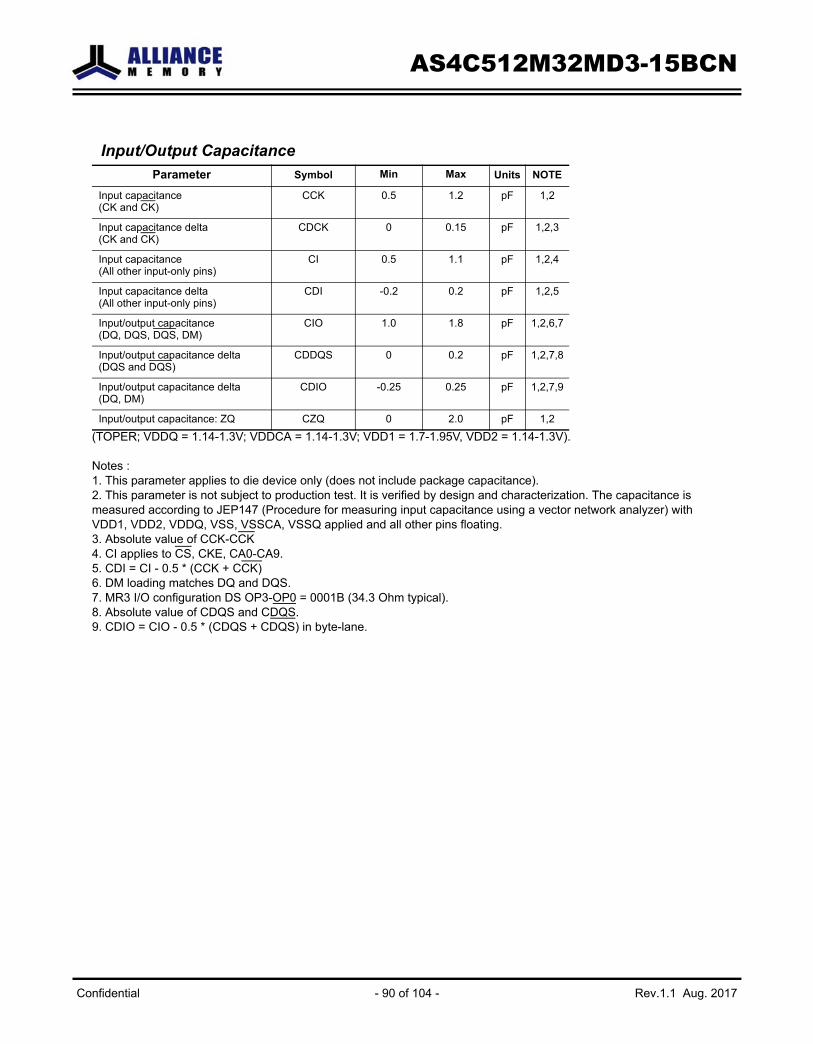
Input/Output Capacitance
(TOPER; VDDQ = 1.14-1.3V; VDDCA = 1.14-1.3V; VDD1 = 1.7-1.95V, VDD2 = 1.14-1.3V).
Notes : 1. This parameter applies to die device only (does not include package capacitance).2. This parameter is not subject to production test. It is verified by design and characterization. The capacitance is measured according to JEP147 (Procedure for measuring input capacitance using a vector network analyzer) with VDD1, VDD2, VDDQ, VSS, VSSCA, VSSQ applied and all other pins floating.3. Absolute value of CCK-CCK4. CI applies to CS, CKE, CA0-CA9.5. CDI = CI - 0.5 * (CCK + CCK)6. DM loading matches DQ and DQS.7. MR3 I/O configuration DS OP3-OP0 = 0001B (34.3 Ohm typical).8. Absolute value of CDQS and CDQS.9. CDIO = CIO - 0.5 * (CDQS + CDQS) in byte-lane.
Parameter Symbol Min Max Units NOTE
Input capacitance(CK and CK)
CCK 0.5 1.2 pF 1,2
Input capacitance delta(CK and CK)
CDCK 0 0.15 pF 1,2,3
Input capacitance(All other input-only pins)
CI 0.5 1.1 pF 1,2,4
Input capacitance delta(All other input-only pins)
CDI -0.2 0.2 pF 1,2,5
Input/output capacitance(DQ, DQS, DQS, DM)
CIO 1.0 1.8 pF 1,2,6,7
Input/output capacitance delta(DQS and DQS)
CDDQS 0 0.2 pF 1,2,7,8
Input/output capacitance delta(DQ, DM)
CDIO -0.25 0.25 pF 1,2,7,9
Input/output capacitance: ZQ CZQ 0 2.0 pF 1,2
AS4C512M32MD3-15BCN
Confidential - 90 of 104 - Rev.1.1 Aug. 2017

AS4C512M32MD3-15BCN
IDD Specification
(VDD2, VDDQ,VDDCA = 1.14~1.30V, VDD1 = 1.70~1.95V)
Conditions Symbol Power Supply 1333 Unit
Operating One Bank Active-Precharge Current:tCK = tCK(avg)min; tRC = tRCmin; CKE is HIGH; CS is HIGH between valid commands; CA bus inputs are SWITCHING; Data bus inputs are STABLEODT disabled
IDD01IDD02IDD0IN
VDD1VDD2
VDDCA,VDDQ
8357
mA
Idle power-down standby current:tCK = tCK(avg)min; CKE is LOW; CS is HIGH; All banks/RBs idle; CA bus inputs are SWITCHING; Data bus inputs are STABLEODT disabled
IDD2P1IDD2P2IDD2PIN
VDD1VDD2
VDDCA,VDDQ
0.52
0.2mA
Idle power-down standby current with clock stop:CK =LOW, CK =HIGH; CKE is LOW; CS is HIGH; All banks/RBs idle; CA bus inputs are STABLE; Data bus inputs are STABLEODT disabled
IDD2PS1IDD2PS2IDD2PSIN
VDD1VDD2
VDDCA,VDDQ
0.52
0.2mA
Idle non power-down standby current:tCK = tCK(avg)min; CKE is HIGH; CS is HIGH; All banks/RBs idle; CA bus inputs are SWITCHING; Data bus inputs are STABLEODT disabled
IDD2N1IDD2N2IDD2NIN
VDD1VDD2
VDDCA,VDDQ
257
mA
Idle non power-down standby current with clock stop: CK_t =LOW, CK_c =HIGH; CKE is HIGH; CS is HIGH; All banks/RBs idle; CA bus inputs are STABLE; Data bus inputs are STABLEODT disabled
IDD2NS1IDD2NS2IDD2NSIN
VDD1VDD2
VDDCA,VDDQ
257
mA
Confidential - 91 of 104 - Rev.1.1 Aug. 2017

AS4C512M32MD3-15BCN
Active power-down standby current: tCK = tCK(avg)min; CKE is LOW; CS is HIGH; One bank/RB active; CA bus inputs are SWITCHING; Data bus inputs are STABLEODT disabled
IDD3P1IDD3P2IDD3PIN
VDD1VDD2
VDDCA,VDDQ
26
0.2mA
Active power-down standby current with clock stop:CK=LOW, CK=HIGH; CKE is LOW; CS is HIGH; One bank/RB active; CA bus inputs are STABLE; Data bus inputs are STABLEODT disabled
IDD3PS1IDD3PS2IDD3PSIN
VDD1VDD2
VDDCA,VDDQ
26
0.2mA
Active non power-down standby current: tCK = tCK(avg)min; CKE is HIGH; CS is HIGH; One bank/RB active; CA bus inputs are SWITCHING; Data bus inputs are STABLEODT disabled
IDD3N1IDD3N2IDD3NIN
VDD1VDD2
VDDCA,VDDQ
287
mA
Active non power-down standby current with clock stop: CK=LOW, CK=HIGH; CKE is HIGH; CS is HIGH; One bank/RB active; CA bus inputs are STABLE; Data bus inputs are STABLEODT disabled
IDD3NS1IDD3NS2IDD3NSIN
VDD1VDD2
VDDCA,VDDQ
267
mA
Operating burst read current: tCK = tCK(avg)min; CS is HIGH between valid commands; One bank/RB active; BL = 4; RL = RLmin; CA bus inputs are SWITCHING; 50% data change each burst transferODT disabled
IDD4R1IDD4R2IDD4RINIDD4RQ
VDD1VDD2
VDDCAVDDQ
2220
7230
mA
Operating burst write current: tCK = tCK(avg)min; CS is HIGH between valid commands; One bank/RB active; BL = 4; WL = WLmin; CA bus inputs are SWITCHING; 50% data change each burst transferODT disabled
IDD4W1IDD4W2IDD4WIN
VDD1VDD2
VDDCA,VDDQ
221025
mA
Conditions Symbol Power Supply 1333 Unit
Confidential - 92 of 104 - Rev.1.1 Aug. 2017

AS4C512M32MD3-15BCN
C
Notes:1. Published IDD values are the maximum of the distribution of the arithmetic mean.2. ODT disabled: MR11[2:0] = 000B.3. IDD current specifications are tested after the device is properly initialized.
All Bank Refresh Burst current: tCK = tCK(avg)min; CKE is HIGH between valid commands; tRC = tRFCabmin; Burst refresh;CA bus inputs are SWITCHING; Data bus inputs are STABLEODT disabled
IDD51IDD52IDD5IN
VDD1VDD2
VDDCA,VDDQ
30149
7mA
All Bank Refresh Average current:
tCK = tCK(avg)min;
CKE is HIGH between valid commands;
tRC = tREFI;
CA bus inputs are SWITCHING;
Data bus inputs are STABLE
ODT disabled
IDD5AB1IDD5AB2IDD5ABIN
VDD1VDD2
VDDCA,VDDQ
4107
mA
Per Bank Refresh Average current:
tCK = tCK(avg)min;
CKE is HIGH between valid commands;
tRC = tREFI/8;
CA bus inputs are SWITCHING;
Data bus inputs are STABLE
ODT disabled
IDD5PB1IDD5PB2IDD5PBIN
VDD1VDD2
VDDCA,VDDQ
4107
mA
Self refresh current (Standard Temperature Range): CK=LOW, CK=HIGH;CKE is LOW; CA bus inputs are STABLE; Data bus inputs are STABLE;Maximum 1x Self-Refresh RateODT disabled
IDD61IDD62IDD6IN
VDD1VDD2
VDDCA,VDDQ
13.80.2
mA
Self refresh current (+85’C to +105’C): CK=LOW, CK=HIGH;CKE is LOW; CA bus inputs are STABLE; Data bus inputs are STABLE;ODT disabled
IDD6ET1IDD6ET2IDD6ETIN
VDD1VDD2
VDDCA,VDDQ
2.53120.4
mA
Deep power-down current: CK=LOW, CK=HIGH;CKE is LOW; CA bus inputs are STABLE; Data bus inputs are STABLE;ODT disabled
IDD81IDD82IDD8IN
VDD1VDD2
VDDCA,VDDQ
20100200
uA
Conditions Symbol Power Supply 1333 Unit
onfidential - 93 of 104 - Rev.1.1 Aug. 2017

AS4C512M32MD3-15BCN
C
4. Measured currents are the summation of VDDQ and VDDCA.5. Guaranteed by design with output load of 5PF and RON = 40Ohm.6. The 1x self refresh rate is the rate at which the device is refreshed internally during self refresh, before going into theextended temperature range.7. This is the general definition that applies to full-array SELF REFRESH.8. IDD6ET is typical values, is sampled only, and is not tested.
IDD6 Partial Array Self-Refresh Current
Notes:1. IDD6 currents are measured using bank-masking only.2. IDD values published are the maximum of the distribution of the arithmetic mean.
PASR Supply 1333 Unit
Full ArrayVDD1VDD2
VDDCA,VDDQ
13.80.2
mA
1/2 ArrayVDD1VDD2
VDDCA,VDDQ
0.792.830.2
mA
1/4 ArrayVDD1VDD2
VDDCA,VDDQ
0.692.340.2
mA
1/8 ArrayVDD1VDD2
VDDCA,VDDQ
0.632.090.2
mA
onfidential - 94 of 104 - Rev.1.1 Aug. 2017

REFRESH Requirements by Device Density
LPDDR3 Refresh Requirement Parameters (per density)
LPDDR3 Read and Write Latencies
Notes:1. RL=3/WL=1 setting is an optional feature. Refer to MR0 OP<7>.2. Write Latency (Set B) support is an optional feature. Refer to MR0 OP<6>.
Symbol Parameter 4Gb(Single Die) 16Gb(Four Dies) Unit
Number of banks 8
tREFW Refresh window: TCASE =< 85’C 32 ms
tREFW Refresh window: 1/2-Rate Refresh 16 ms
tREFW Refresh window: 1/4-Rate Refresh 8 ms
R Required number of REFRESH commands (MIN) 8192 8192
tREFI Average time between REFRESH commands (for reference only) TCASE <= 85’C
3.9 3.9 us
tREFIpb 0.4875 0.4875 us
tRFCab Refresh cycle time 130 130 ns
tRFCpb Per-bank REFRESH cycle time 60 60 ns
Parameter Value Unit
Max. Clock Frequency 166 400 533 600 667 MHz
Max. Data Rate 333 800 1066 1200 1333 MT/s
Average Clock Period 6 2.5 1.875 1.67 1.5 ns
Read Latency 31 6 8 9 10 tCK(avg)
Write Latency (Set A) 11 3 4 5 6 tCK(avg)
Write Latency (Set B)2 11 3 4 5 8 tCK(avg)
AS4C512M32MD3-15BCN
Confidential - 95 of 104 - Rev.1.1 Aug. 2017

AS4C512M32MD3-15BCN
AC Characteristics(VDD2, VDDQ,VDDCA = 1.14~1.30V, VDD1 = 1.70~1.95V)Notes 1, 2, 3 and 4 apply to all parameters. Notes begin below table.
Parameter Symbol min/maxSpeed Grade
Unit1333
Clock Timing
Max. Frequency fCK ~ 667 MHz
Average Clock Period tCK(avg)min 1.5
nsmax 100
Average HIGH pulse width tCH(avg)min 0.45
tCK(avg)max 0.55
Average LOW pulse width tCL(avg)min 0.45
tCK(avg)max 0.55
Absolute Clock Period tCK(abs) min tCK(avg) min + tJIT(per) min ps
Absolute clock HIGH pulse width tCH(abs)min 0.43
tCK(avg)max 0.57
Absolute clock LOW pulse width tCL(abs)min 0.43
tCK(avg)max 0.57
Clock Period Jitter (with supported jitter)
tJIT(per),allowed
min -80ps
max 80
Maximum Clock Jitter between two consecutive clock cycles (with allowed jitter)
tJIT(cc),allowed
max 160 ps
Duty cycle Jitter (with supported jitter)
tJIT(duty),allowed
min min((tCH(abs),min - tCH(avg),min), (tCL(abs),min - tCL(avg),min)) * tCK(avg)
psmax max((tCH(abs),max - tCH(avg),max), (tCL(abs),max -
tCL(avg),max)) * tCK(avg)
Cumulative error across 2 cycles tERR(2per), allowed
min -118ps
max 118
Cumulative error across 3 cycles tERR(3per), allowed
min -140ps
max 140
Cumulative error across 4 cycles tERR(4per), allowed
min -155ps
max 155
Cumulative error across 5 cycles tERR(5per), allowed
min -168ps
max 168
Cumulative error across 6 cycles tERR(6per), allowed
min -177ps
max 177
Cumulative error across 7 cycles tERR(7per), allowed
min -186ps
max 186
Confidential - 96 of 104 - Rev.1.1 Aug. 2017

AS4C512M32MD3-15BCN
Cumulative error across 8 cycles tERR(8per), allowed
min -193ps
max 193
Cumulative error across 9 cycles tERR(9per), allowed
min -200ps
max 200
Cumulative error across 10 cycles tERR(10per), allowed
min -205ps
max 205
Cumulative error across 11 cycles tERR(11per),allowed
min -210ps
max 210
Cumulative error across 12 cycles tERR(12per),allowed
min -215ps
max 215
Cumulative error across n = 13, 14, 15. . . 19, 20cycles
tERR(nper),allowed
min tERR(nper),allowed min = (1 + 0.68ln(n)) * tJIT(per),allowed min
psmax tERR(nper),allowed max = (1 + 0.68ln(n)) *
tJIT(per),allowed max
ZQ Calibration Parameters
Initialization Calibration Time tZQINIT min 1 us
Long Calibration Time tZQCL min 360 ns
Short Calibration Time tZQCS min 90 ns
Calibration Reset Time tZQRESET min max(50ns,3nCK) ns
Read Parameters5
DQS output access time from CK/CK tDQSCKmin 2500
psmax 5500
DQSCK Delta Short tDQSCKDS max 265 ps
DQSCK Delta Medium tDQSCKDM max 593 ps
DQSCK Delta Long tDQSCKDL max 733 ps
DQS - DQ skew tDQSQ max 165 ps
DQS Output High Pulse Width tQSH min tCH(abs) - 0.05 tCK(avg)
DQS Output Low Pulse Width tQSL min tCL(abs) - 0.05 tCK(avg)
DQ / DQS output hold time from DQS tQH min min(tQSH, tQSL) ps
Read preamble tRPRE min 0.9 tCK(avg)
Read postamble tRPST min 0.3 tCK(avg)
DQS low-Z from clock tLZ(DQS) min tDQSCK(MIN) - 300 ps
DQ low-Z from clock tLZ(DQ) min tDQSCK(MIN) - 300 ps
DQS high-Z from clock tHZ(DQS) max tDQSCK(MAX) - 100 ps
DQ high-Z from clock tHZ(DQ) max tDQSCK(MAX) + (1.4 * tDQSQ(MAX)) ps
Parameter Symbol min/maxSpeed Grade
Unit1333
Confidential - 97 of 104 - Rev.1.1 Aug. 2017

AS4C512M32MD3-15BCN
Write Parameters5
DQ and DM input hold time (Vref based) tDH min 175 ps
DQ and DM input setup time (Vref based) tDS min 175 ps
DQ and DM input pulse width tDIPW min 0.35 tCK(avg)
Write command to 1st DQS latching transition tDQSSmin 0.75
tCK(avg)max 1.25
DQS input high-level width tDQSH min 0.4 tCK(avg)
DQS input low-level width tDQSL min 0.4 tCK(avg)
DQS falling edge to CK setup time tDSS min 0.2 tCK(avg)
DQS falling edge hold time from CK tDSH min 0.2 tCK(avg)
Write postamble tWPST min 0.4 tCK(avg)
Write preamble tWPRE min 0.8 tCK(avg)
CKE Input Parameters
CKE min. pulse width (high and low pulse width)
tCKE min max(7.5ns,3nCK) tCK(avg)
CKE input setup time tISCKE14 min 0.25 tCK(avg)
CKE input hold time tIHCKE15 min 0.25 tCK(avg)
Command path disable delay tCPDED min 2 tCK(avg)
Command Address Input Parameters5
Address and control input setup time tISCA16 min 175 ps
Address and control input hold time tIHCA16 min 175 ps
CS input setup time tISCS16 min 290 ps
CS input hold time tIHCS16 min 290 ps
Address and control input pulse width tIPWCA min 0.35 tCK(avg)
CS input pulse width tIPWCS min 0.7 tCK(avg)
Boot Parameters (10 MHz - 55 MHz)16, 17, 18
Clock cycle time tCKbmax 100
nsmin 18
CKE input setup time tISCKEb min 2.5 tCK(avg)
CKE input hold time tIHCKEb min 2.5 tCK(avg)
Address and control input setup time tISb min 1150 ps
Address and control input hold time tIHb min 1150 ps
DQS output data access time from CK/CK tDQSCKbmin 2
nsmax 10
Data strobe edge to output data edge tDQSQb max 1.2 ps
Parameter Symbol min/maxSpeed Grade
Unit1333
Confidential - 98 of 104 - Rev.1.1 Aug. 2017

AS4C512M32MD3-15BCN
Mode Register Parameters
MODE REGISTER Write command period tMRW min 10 tCK(avg)
Mode Register Read command period tMRR min 4 tCK(avg)
Additional time after tXP has expired untilMRR command may be issued
tMRRI min tRCD(MIN) ns
Core Parameters20
Read Latency RL min 10 tCK(avg)
Write Latency (set A) WL min 6 tCK(avg)
Write Latency (set B) WL min 8 tCK(avg)
ACTIVE to ACTIVE command period tRC min tRAS + tRPab (with all-bank Precharge)tRAS + tRPpb (with per-bank Precharge)
ns
CKE min. pulse width during Self-Refresh (low pulse width during Self-Refresh)
tCKESR min max(15ns,3nCK) ns
Self refresh exit to next valid command delay tXSR min max(tRFCab + 10ns,2nCK) ns
Exit power down to next valid command delay tXP min max(7.5ns,3nCK) ns
CAS to CAS delay tCCD min 4 tCK(avg)
Internal Read to Precharge command delay tRTP min max(7.5ns,4nCK) ns
RAS to CAS DelaytRCD(fast)
minmax(15ns,3nCK)
nstRCD(typ) max(18ns,3nCK)
tRCD(slow) max(24ns,3nCK)
Row Precharge Time(single bank)tRPpb(fast)
minmax(15ns,3nCK)
nstRPpb(typ) max(18ns,3nCK)
tRPpb(slow) max(24ns,3nCK)
Row Precharge Time(all bank)tRPab(fast)
minmax(18ns,3nCK)
nstRPab(typ) max(21ns,3nCK)
tRPab(slow) max(27ns,3nCK)
Row Active Time tRASmin max(42ns,3nCK) ns
max 70 us
Write Recovery Time tWR min max(15ns,4nCK) ns
Internal Write to Read Command Delay tWTR min max(7.5ns,4nCK) ns
Active bank A to Active bank B tRRD min max(10ns,2nCK) ns
Four Bank Activate Window tFAW min max(50ns,8nCK) ns
Minimum Deep Power Down Time tDPD min 500 us
ODT Parameters
Parameter Symbol min/maxSpeed Grade
Unit1333
Confidential - 99 of 104 - Rev.1.1 Aug. 2017

)
)
)
)
)
)
AS4C512M32MD3-15BCN
C
Asynchronous RTT turn-on dely from ODTinput
tODTonmin 1.75
nsmax 3.5
Asynchronous RTT turn-off delay from ODTinput
tODToffmin 1.75
nsmax 3.5
Automatic RTT turn-on delay after READdata
tAODTon max tDQSCK + 1.4 x tDQSQ,max + tCK(avg,min) ps
Automatic RTT turn-off delay after READdata
tAODToff min tDQSCK,min - 300 ps
RTT disable delay from power down,self-refresh, and deep power down entry
tODTd max 12 ns
RTT enable delay from power down and selfrefresh exit
tODTe max 12 ps
CA Training Parameters
First CA calibration command after CAcalibration mode is programmed
tCAMRD min 20 tCK(avg
First CA calibration command after CKE isLOW
tCAENT min 10 tCK(avg
CA caibration exit command after CKE isHIGH
tCAEXT min 10 tCK(avg
CKE LOW after CA calibration mode isprogrammed
tCACKEL min 10 tCK(avg
CKE HIGH after the last CA calibration resultsare driven
tCACKEH min 10 tCK(avg
Data out delay after CA training calibrationcommand is programmed
tADR max 20 ns
MRW CA exit command to DQ tri-state tMRZ min 3 ns
CA calibration command to CA calibrationcommand delay
tCACD min RU(tADR+2 x tCK) tCK(avg
Write Leveling Parameters
DQS/DQS delay after write leveling mode isprogrammed tWLDQSEN
min 25ns
max -
First DQS/DQS edge after write level-ingmode is programmed tWLMRD
min 40ns
max -
Write leveling output delay tWLOmin 0
nsmax 20
Write leveling hold time tWLH min 205 ps
Write leveling setup time tWLS min 205 ps
Parameter Symbol min/maxSpeed Grade
Unit1333
onfidential - 100 of 104 - Rev.1.1 Aug. 2017

AS4C512M32MD3-15BCN
C
Notes for AC Electrical Characteristics1. Frequency values are for reference only. Clock cycle time (tCK) is used to determine device capabilities.2. All AC timings assume an input slew rate of 2 V/ns for single ended signals.3. Measured with 4 V/ns differential CK_t/CK_c slew rate and nominal VIX.4. All timing and voltage measurements are defined “at the ball”.5. READ, WRITE, and input setup and hold values are referenced to VREF.6. tDQSCKDS is the absolute value of the difference between any two tDQSCK measurements (in a byte lane) within a
contig-uous sequence of bursts in a 160ns rolling window. tDQSCKDS is not tested and is guaranteed by design. Tem-perature drift in the system is < 10 ‘C/s. Values do not include clock jitter.7. tDQSCKDM is the absolute value of the difference between any two tDQSCK measurements (in a byte lane) within a
1.6us rolling window. tDQSCKDM is not tested and is guaranteed by design. Temperature drift in the system is < 10 ‘C/s. Values do not include clock jitter.8. tDQSCKDL is the absolute value of the difference between any two tDQSCK measurements (in a byte lane) within a
32ms rolling window. tDQSCKDL is not tested and is guaranteed by design. Temperature drift in the system is < 10 ‘C/s.Values do not include clock jitter..9. TFor LOW-to-HIGH and HIGH-to-LOW transitions, the timing reference is at the point when the signal crosses the
tran-sition threshold (VTT). tHZ and tLZ transitions occur in the same access time (with respect to clock) as valid datatransitions. These parameters are not referenced to a specific voltage level but to the time when the device output is nolonger driving (for tRPST, tHZ(DQS) and tHZ(DQ)), or begins driving (for tRPRE, tLZ(DQS), tLZ(DQ)). The figure belowshows a method to calculate the point when device is no longer driving tHZ(DQS) and tHZ(DQ), or begins drivingtLZ(DQS), tLZ(DQ) by measuring the signal at two different volt-ages. The actual voltage measurement points are notcritical as long as the calculation is consistent.10. Output Transition Timing
Mode register set command delay tMRDmin max(14ns, 10nCK )
nsmax -
Temperature Derating19
DQS output access time from CK/CK(derated)
tDQSCK max 5620 ps
RAS-to-CAS delay (derated) tRCD min tRCD + 1.875 ns
ACTIVATE-to- ACTIVATE command period(derated)
tRC min tRC + 1.875 ns
Row active time (derated) tRAS min tRAS + 1.875 ns
Row precharge time (derated) tRP min tRP + 1.875 ns
Active bank A to active bank B (derated) tRRD min tRRD + 1.875 ns
Parameter Symbol min/maxSpeed Grade
Unit1333
onfidential - 101 of 104 - Rev.1.1 Aug. 2017

AS4C512M32MD3-15BCN
C
11. The parameters tLZ(DQS), tLZ(DQ), tHZ(DQS), and tHZ(DQ) are defined as single-ended. The timing parameterstRPRE and tRPST are determined from the differential signal DQS/DQS.12. Measured from the point when DQS/DQS begins driving the signal to the point when DQS/DQS begins driving thefirst rising strobe edge.13. Measured from the last falling strobe edge of DQS/DQS to the point when DQS/DQS finishes driving the signal.14. CKE input setup time is measured from CKE reaching a HIGH/LOW voltage level to CK/CK crossing.15. CKE input hold time is measured from CK/CK crossing to CKE reaching a HIGH/LOW voltage level.16. Input set-up/hold time for signal (CA[9:0], CS).17. To ensure device operation before the device is configured, a number of AC boot-timing parameters are defined inthis table. Boot parameter symbols have the letter b appended (for example, tCK during boot is tCKb).18. The LPDDR3 device will set some mode register default values upon receiving a RESET (MRW) command as spec-ified in Mode Register Definition.19. The output skew parameters are measured with default output impedance settings using the reference load.20. The minimum tCK column applies only when tCK is greater than 6ns.
tHZ(DQS), tHZ(DQ)
stop driving point = 2 x T1 - T2
VOL + 2x X mV
T1 T2
VOL + X mV
VOH - X mV
VOH - 2x X mVtLZ(DQS), tLZ(DQ)
begin driving point = 2 x T1 - T2
VOL
VTT - Y mV
VOH
T2T1
VTT - 2x Y mV
VTT + 2x Y mV
VTT + Y mV
VTTVTTY
2x Yactual waveform
X2x X
onfidential - 102 of 104 - Rev.1.1 Aug. 2017

Package Diagram178-Ball FBGA - 11.0mm x 11.5mm 0.65mm/0.8mm pitch
Vref(CA)
b
CA2b
CA2b
CA2b
CA2b
CA2b
CA2b
CA2b
CA2b
Vref(CA)
b
CA2b
Vref(CA)
b
DQ6a
VSSQ
a
VDDQ
a
R
T
Bottom View
0.5
50 ±
0.1
00
11.5
00
±0
.100
0.6
50
A
B
C
D
E
F
G
H
J
K
L
M
N
P
U
12345678910111213
11.000 ± 0.100
0.800 x 12 = 9.600
0.6
50 x
16 =
10.4
00
178 x Ø0.300±0.050(Post Reflow Ø0.320±0.050)
Ø0.15 M C A B
0.2
20 ±
0.0
50
SEATING PLANE
C
0.10 C
0.9
30 ±
0.0
70
Front View
Unit: mm
A1 INDEX MARK
VDD1a
VDD2a/b
DQ1
a
VDDQ
a
VSSQa
DQ0a
DM2a
VDDQa
DQS2_ta
DQS2_ca
VSSQa
DQ23a
VDDQ
a
DQ22
a
DQ20a
DQ21a
DQ19a
VSSQa
VDDQa
DQ18a
DQ16a
DQ17a
VDD2
b
VDD1
b
VSSb
CA0b
VDDCAb
CA1b
Vref
(CA)b
CA2b
0.700 ± 0.100 0.800
DNU
VDDQ
a
VDD2a/b
VDDQ
a
DQ0a
VDDQa
DQS2_ca
DQ23a
DQ22
a
DQ21a
VSSQa
DQ18a
DQ17a
VDD1
b
CA0b
CA1b
CA2b
DQ6a
VDDQ
a
VDD2a/b
VDDQ
a
DQ0a
VDDQa
DQS2_ca
DQ23a
DQ22
a
DQ21a
VSSQa
DQ18a
DQ17a
VDD1
b
CA0b
CA1b
CA2b
DNUDQ6
a
VDDQ
a
VDD2a/b
VDDQ
a
DQ0a
VDDQa
DQS2_ca
DQ23a
DQ22
a
DQ21a
VSSQa
DQ18a
DQ17a
VDD1
b
CA0b
CA1b
CA2b
DQ6a
VDDQ
a
CA1b
CA2b
DQ6a
VSSQ
a
VDDQ
a
VDD1a
VDD2a/b
DQ1
a
VDDQ
a
VSSQa
DQ0a
DM2a
VDDQa
DQS2_ta
DQS2_ca
VSSQa
DQ23a
VDDQ
a
DQ22
a
DQ20a
DQ21a
DQ19a
VSSQa
VDDQa
DQ18a
DQ16a
DQ17a
VDD2
b
VDD1
b
VSSb
CA0b
VDDCAb
CA1b
CA2b
DNU
VDDQ
a
VDD2a/b
VDDQ
a
DQ0a
VDDQa
DQS2_ca
DQ23a
DQ22
a
DQ21a
VSSQa
DQ18a
DQ17a
VDD1
b
CA0b
CA1b
CA2b
DQ6a
VDDQ
a
VDD2a/b
VDDQ
a
DQ0a
VDDQa
DQS2_ca
DQ23a
DQ22
a
DQ21a
VSSQa
DQ18a
DQ17a
VDD1
b
CA0b
CA1b
CA2b
DNU
VSSQ
a
VDDCAb
Vref
(CA)b
CA2b
DNU
VDD1a
DQ1
a
VSSQa
DM2a
DQS2_ta
VSSQa
VDDQ
a
DQ20a
DQ19a
VDDQa
DQ16a
VDD2
b
VSSb
VSSQ
a
VDDCAb
Vref
(CA)b
DNU
AS4C512M32MD3-15BCN
Confidential - 103 of 104 - Rev.1.1 Aug. 2017

PART NUMBERING SYSTEM AS4C 512M32MD3 15 B C N
DRAM 15=667MHz B=FBGA C=Commercial (-25°C~+85°C)
IndicatesPbandHalogenFree
Alliance Memory, Inc. 511 Taylor Way, San Carlos, CA 94070 Tel: 650-610-6800Fax: 650-620-9211www.alliancememory.com
Copyright © Alliance Memory All Rights Reserved
© Copyright 2007 Alliance Memory, Inc. All rights reserved. Our three-point logo, our name and Intelliwatt are trademarks or registered trademarks of Alliance. All other brand and product names may be the trademarks of their respective companies. Alliance reserves the right to make changes to this document and its products at any time without notice. Alliance assumes no responsibility for any errors that may appear in this document. The data contained herein represents Alliance's best data and/or estimates at the time of issuance. Alliance reserves the right to change or correct this data at any time, without notice. If the product described herein is under development, significant changes to these specifications are possible. The information in this product data sheet is intended to be general descriptive information for potential customers and users, and is not intended to operate as, or provide, any guarantee or warrantee to any user or customer. Alliance does not assume any responsibility or liability arising out of the application or use of any product described herein, and disclaims any express or implied warranties related to the sale and/or use of Alliance products including liability or warranties related to fitness for a particular purpose, merchantability, or infringement of any intellectual property rights, except as express agreed to in Alliance's Terms and Conditions of Sale (which are available from Alliance). All sales of Alliance products are made exclusively according to Alliance's Terms and Conditions of Sale. The purchase of products from Alliance does not convey a license under any patent rights, copyrights; mask works rights, trademarks, or any other intellectual property rights of Alliance or third parties. Alliance does not authorize its products for use as critical components in life-supporting systems where a malfunction or failure may reasonably be expected to result in significant injury to the user, and the inclusion of Alliance products in such life-supporting systems implies that the manufacturer assumes all risk of such use and agrees to indemnify Alliance against all claims arising from such use.
512M32=512MX32 MD3=Mobile
DDR3
AS4C512M32MD3-15BCN
Confidential - 104 of 104 - Rev.1.1 Aug. 2017

![4Gb E-die DDR3 SDRAM - samsung.com · - 5 - K4B4G0846E datasheet DDR3 SDRAM Rev. 1.2 K4B4G0446E 1. Ordering Information [ Table 1 ] Samsung 4Gb DDR3 E-die ordering information table](https://static.fdocuments.us/doc/165x107/5dd0e76fd6be591ccb634357/4gb-e-die-ddr3-sdram-5-k4b4g0846e-datasheet-ddr3-sdram-rev-12-k4b4g0446e.jpg)


![4Gb A-die DDR3 SDRAM - МТ System · DDR3 SDRAM Addressing ... 11. 4Gb DDR3 SDRAM A-die IDD Specification Table ... [ Table 1 ] Samsung 4Gb DDR3 A-die ordering information table](https://static.fdocuments.us/doc/165x107/5ad5dbf67f8b9a5c638d9a55/4gb-a-die-ddr3-sdram-sdram-addressing-11-4gb-ddr3-sdram-a-die-idd-specification.jpg)


![1Gb G-die DDR3 SDRAM x16 only - TechPowerUp€¦ · DDR3 SDRAM Addressing ... [ Table 1 ] Samsung 1Gb DDR3 G-die ordering information table. NOTE: 1. Speed bin is in order of CL-tRCD-tRP.](https://static.fdocuments.us/doc/165x107/5ad5dbf67f8b9a5c638d9a56/1gb-g-die-ddr3-sdram-x16-only-techpowerup-ddr3-sdram-addressing-table.jpg)