Ali Adibi GEORGIA TECH RESEARCH CORPORATION 03/07/2019 ...
28
AFRL-AFOSR-VA-TR-2019-0155 Nonlinear Optical Signal Processing On Chip: A New Paradigm for Implementation of Optical Logic Functionality Ali Adibi GEORGIA TECH RESEARCH CORPORATION Final Report 03/07/2019 DISTRIBUTION A: Distribution approved for public release. AF Office Of Scientific Research (AFOSR)/ RTB1 Arlington, Virginia 22203 Air Force Research Laboratory Air Force Materiel Command DISTRIBUTION A: Distribution approved for public release.
Transcript of Ali Adibi GEORGIA TECH RESEARCH CORPORATION 03/07/2019 ...

AFRL-AFOSR-VA-TR-2019-0155
Nonlinear Optical Signal Processing On Chip: A New Paradigm for Implementation of OpticalLogic Functionality
Ali AdibiGEORGIA TECH RESEARCH CORPORATION
Final Report03/07/2019
DISTRIBUTION A: Distribution approved for public release.
AF Office Of Scientific Research (AFOSR)/ RTB1Arlington, Virginia 22203
Air Force Research Laboratory
Air Force Materiel Command
DISTRIBUTION A: Distribution approved for public release.

REPORT DOCUMENTATION PAGE Form ApprovedOMB No. 0704-0188
1. REPORT DATE (DD-MM-YYYY) 2. REPORT TYPE
4. TITLE AND SUBTITLE 5a. CONTRACT NUMBER
6. AUTHOR(S)
7. PERFORMING ORGANIZATION NAME(S) AND ADDRESS(ES)
9. SPONSORING/MONITORING AGENCY NAME(S) AND ADDRESS(ES)
8. PERFORMING ORGANIZATIONREPORT NUMBER
10. SPONSOR/MONITOR'S ACRONYM(S)
13. SUPPLEMENTARY NOTES
12. DISTRIBUTION/AVAILABILITY STATEMENT
14. ABSTRACT
15. SUBJECT TERMS
18. NUMBEROFPAGES
19a. NAME OF RESPONSIBLE PERSON a. REPORT b. ABSTRACT c. THIS PAGE
17. LIMITATION OFABSTRACT
Standard Form 298 (Rev. 8/98)Prescribed by ANSI Std. Z39.18
Adobe Professional 7.0
PLEASE DO NOT RETURN YOUR FORM TO THE ABOVE ORGANIZATION. 3. DATES COVERED (From - To)
5b. GRANT NUMBER
5c. PROGRAM ELEMENT NUMBER
5d. PROJECT NUMBER
5e. TASK NUMBER
5f. WORK UNIT NUMBER
11. SPONSOR/MONITOR'S REPORTNUMBER(S)
16. SECURITY CLASSIFICATION OF:
19b. TELEPHONE NUMBER (Include area code)
The public reporting burden for this collection of information is estimated to average 1 hour per response, including the time for reviewing instructions, searching existing data sources, gathering andmaintaining the data needed, and completing and reviewing the collection of information. Send comments regarding this burden estimate or any other aspect of this collection of information, includingsuggestions for reducing the burden, to the Department of Defense, Executive Service Directorate (0704-0188). Respondents should be aware that notwithstanding any other provision of law, noperson shall be subject to any penalty for failing to comply with a collection of information if it does not display a currently valid OMB control number.
07-03-2019 Final Report 1/9/2015-31/8/2018
Hybrid Nonlinear Optical Signal Processing on Chip: A New Paradigm for Implementation of Optical Logic Functionality
FA9550-15-1-0342
Ali Adibi (PI), Ali A. Eftekhar (co-PI)
Georgia Tech Research Corporation505 10th StreetAtlanta, GA 30332-0415
AFOSR801 N Randolph St.Arlington VA 22203
Approved for public release; distribution unlimited
This program resulted in a solid framework for enabling on-chip nonlinear optical processing through realization of five solid material and device platforms with unique features, for the first time: 1) multi-layer Si/SiN/SiC material platform for nonlinear optics, quantum photonics, and optoelectronic applications (including the demonstration of the coupling modulator architecture for low-power wideband devices), 2) a hybrid material platform formed by integration of phase-change materials with Si/SiN for miniaturized ultra-low-power optoelectronic and nonlinear photonic devices, 3) a hybrid active material platform formed by integration of two-dimensional transition metal dichalcogenides with CMOS-compatible substrates with the possibility of forming lateral heterostructures through a simple annealing process for the formation of active and nonlinear devices, 4) an integrated photonic/phononic material and device platform for nonlinear devices based on combined acoustic and optical waves (e.g., SBS-based devices), and 5) an integrated material platform based on an engineered array of plasmonic nanostructures for sensing and nonlinear optics on chip. The research in this program resulted in over 20 journal papers, 25 conference papers, and 20 invited talks.
Integrated nanophotonics, Nonlinear optical signal processing, Active photonic materials and devices, Nonlinear optical materials and devices
U U U UU 26
Ali Adibi
(404)385-2738
DISTRIBUTION A: Distribution approved for public release.
1
Final Report to the
Air Force Office of Scientific Research (AFOSR)
Hybrid Nonlinear Optical Signal Processing on Chip: A
New Paradigm for Implementation of Optical Logic
Functionality
Georgia Institute of Technology
Principal Investigator:
Ali Adibi
Professor, School of Electrical and Computer Engineering,
Georgia Institute of Technology
Atlanta, GA 30332-0250
e-mail:[email protected]
Tel: (404) 385-2738
Fax: (404) 894-4641
DISTRIBUTION A: Distribution approved for public release.

2
I. Introduction
This report summarizes achievements in Dr. Adibi’s research group at Georgia Institute of Technology
under the program supported by grant number FA9550-15-1-0342. This report mainly covers major
achievements from September 1, 2017 until August 31, 2018 with brief descriptions. Achievements in the
previous years of the program are reported in the annual progress reports for similar periods ending in 2016
and 2017. For brevity, only the details of the recent progress after the last report is presented here along
with a short summary of the previous achievements. Detailed information also can be found in the recent
publications or can be directly requested from Dr. Adibi.
The goal of this AFOSR-supported research was to develop efficient, low-power, and high speed
nonlinear photonic material and device platforms for nonlinear optical signal processing that could
potentially enable the concept of optical logic. Considering the limited nonlinear response of the available
CMOS-compatible materials (e.g., silicon (Si) and silicon nitride (SiN)) for integrated nanophotonic
structures, realization of new material platforms and device architectures for realization of competent
nonlinear devices with reasonable performance is an urgent need. This important fundamental task took
most of the resources of this program. Consequently, the program resulted in a solid framework for
enabling on-chip nonlinear optical processing using an arsenal of hybrid CMOS-compatible material
platforms and a series of optimized device architectures. While the duration of the program did not allow
the eventual formation of the “optical logic” structures, the findings of this program can go far beyond the
logic concept and enable urgently needed nonlinear integrated photonic structures for state-of-the-art
applications like reservoir computing, neuromorphic computing, frequency comb generation, stimulated
Brillouin scattering (SBS)-based structures for nonlinear signal processing and laser stabilization,
nonlinear plasmonic and photonic sensing, and many others. Indeed, over a period of three years, this
program resulted in 5 solid material and device platforms with unique features, for the first time: 1) multi-
layer Si/SiN/SiC (silicon carbide) material platform for nonlinear optics, quantum photonics, and
optoelectronic applications (including the demonstration of the coupling modulator architecture for low-
power wideband devices), 2) a hybrid material platform formed by integration of phase-change materials
(PCMs) with Si/SiN for miniaturized ultra-low-power optoelectronic and nonlinear photonic devices
(including the demonstration of bistability on-chip), 3) a hybrid active material platform formed by
integration of two-dimensional transition metal dichalcogenides (2D TMDCs) with CMOS-compatible
substrates (e.g., Si and SiN) with the possibility of forming lateral heterostructures through a simple
annealing process for the formation of active and nonlinear devices (e.g. light emitters and detectors), 4) an
integrated photonic/phononic material and device platform for nonlinear devices based on combined
acoustic and optical waves (e.g., SBS-based devices), and 5) an integrated material platform based on an
engineered array of plasmonic nanostructures for sensing and nonlinear optics on chip (including
demonstration of second harmonic generation (SHG) and sensing of chiral molecules). In addition to the
results of this program, each material/device platform can enable several new devices for a wide range of
applications (some of them listed above). As such, this program was very productive in providing a solid
framework for multiple new programs in the area of integrated photonics for active, passive, and nonlinear
applications. The research in this program has resulted in over 20 journal papers (9 journal papers in
2018), 25 conference papers (11 in 2018), and 20 invited conference and seminar talks (9 In 2018). The
list of the publications that resulted from this research program is included at Section III.
In the first two years of this program, we studied different fundamental nonlinear mechanisms,
materials, and device platforms that enable efficient nonlinear optical signal processing platforms. During
this period, we developed the infrastructure for the analysis, design, optimization, fabrication, and
characterization of the envisioned materials and devices. This resulted in the development of different
simulation tools, fabrication processes, material integration schemes, and characterization tools for
DISTRIBUTION A: Distribution approved for public release.
3
nonlinear integrated photonic materials and devices. The main challenge in the development of a photonic
nonlinear signal processing platform, which can surpass the performance of the conventional signal
processing architectures based on digital electronic approaches (in terms of processing speed and power
consumption) is the lack of on-chip efficient nonlinear mechanisms/materials. Therefore, to overcome this
fundamental challenge, a good portion of our effort in this program was focused on identifying and
development of new nonlinear all-optical mechanisms and alternative material platforms, which can
mitigate this challenge and enable next generation nonlinear photonic devices for signal processing. While
we could not get to the full demonstration of a nonlinear processing device for nonlinear signal processing
in this program, we believe that the long-term impact of the achievements of this fundamental research will
considerably overwhelms the advantages of demonstration of nonlinear processing devices in conventional
material platforms with mediocre performance measures (that do not surpass those of digital electronic
signal processing approaches).
In addition to the completion of work on the material platforms in the first two years (especially the
SBS-devices), we focused in the third year on two material and device platforms for nonlinear devices
namely, 1) 2D TMDCs with lateral heterostructures for adding nonlinearity and active properties to
integrated nanophotonics, and 2) integrated photonic devices with unprecedented performance based on
SiC, which can enable more efficient nonlinear photonic devices and also provide prospects for development
of the necessary building blocks for chip-scale quantum computing. These two platforms are discussed in
details in the rest of this report while briefly discussing the completion of the work of the first two years
(for which separate reports were submitted in earlier years).
II. Research Accomplishments
II.A. Overview of the continuation of the research from previous annual reports
Our research in this program has been focused on developing new platforms for low-power and fast
nonlinear photonic devices, which can harbor the development of new nonlinear signal processing
platforms. In this approach, our work has been focused on multiple facets aiming at developing new hybrid
engineered material and device platforms and the study of their fundamental properties for enabling
ultrafast, low-power, and miniaturized devices and systems for nonlinear signal processing on chip (e.g.,
for optical computing, frequency comb generation and manipulation, and digital logic).
Figure 1 shows an overview of some of the main accomplishments initially reported in the first two
years (and some completed in the third year). We continued on the development of functional hybrid
material platforms for high-speed optoelectronic devices (Figure 1(a)), plasmonic nonlinear photonic
devices, especially second harmonic generation (Figures 1(b) and 1(c)), integrated photonic structures for
comb generation based on dispersion engineering (Figure 1(d)), lateral heterostructures in 2D TMDCs for
nonlinear and quantum photonic applications (Figure 1(e)), novel nonlinear devices through integration of
PCMs with integrated photonic structures (Figure 1(f)), and a new integrated photonic/phononic platform
for realization of SBS on chip. Each one of the resulting platforms can enable a series of devices/systems
for nonlinear photonic applications with the potential to considerably improve the performance measures of
the state-of-the-art structures.
Throughout this program, the potentials of several material systems for realization of nonlinear signal
processing devices and systems were studied. In addition to forming hybrid material and device platforms
using more conventional materials (e.g., Si and SiN), we have investigated the formation of new hybrid
platforms using new materials such as lithium niobate (LiNbO3) [1, 2] and SiC [3, 4]. On the device side,
we have used new approaches for making devices in both the conventional and new material platforms to
improve the nonlinear response. We also have developed fast and efficient nonlinear plasmonic devices
including devices for efficient nonlinear SHG based on quasi-phase matching in plasmonic nanoantenna
DISTRIBUTION A: Distribution approved for public release.

4
arrays (Figure 1(b)) [5] and demonstration of ultra-fast hot-carrier-induced nonlinearity with exceptional
nonlinear amplitude and phase responses [6, 7, 8].
We have also continued our efforts on developing new mechanisms and material platforms for low-
power nonlinear functionalities such as nonlinear signal generation and nonlinear switching including lateral
heterostructures in 2D TMDCs (Figure 1(e)), low-power all-optical phase-transition in PCM nanoparticles
(Figure (1(f)), and the low-threshold optomechanical nonlinearity in devices based on coupling between the
resonant optical and acoustic modes in optomechanical structures as well as SBS in Si waveguides and
resonators (Figure (1(g)). Our research in this areas has been reported in several recent publications
[9,10,11,12].
Figure 1, An overview of the research accomplishment supported by this program. (a) high-speed
optoelectronic devices on hybrid material platforms, (b) Efficient phase-matched SHG in plasmonic
nanoantenna structures, (c) ultra-fast hot-carrier nonlinearity in plasmonic nanostructures, (d) visible comb
signals based on dispersion engineering in different material platforms (e.g., SiN, and LiNbO3), (e) two-
dimensional TMDC alloys and heterostructures, (e) nonlinear bi-stability in hybrid SiN and PCM nanoparticle
structures, and (g) low-power SPS nonlinearity in waveguide and resonator-based SiN devices.
750 800 850 900 9500
500
1000
1500
2000
2500
wavelength, (nm)S
H Inte
nsity (
a.u
.)
p = 520 nm
P = 560 nm
p = 540 nm
LP Mode
Wavelength (nm)
GST SiN resonator
(a) (b) (c)
(d)
(f)
(e)
(g)
FP Mode
DISTRIBUTION A: Distribution approved for public release.
5
II.B. Development of a high-quality SiC material and device platform for nonlinear photonic devices
SiC is a unique semiconductor material for optoelectronic applications as it provides a wide transparency
window; strong thermal, mechanical, and optical properties; and relatively high second-order and third-
order nonlinearities. The large indirect bandgap (> 2.2 eV) and high index of refraction (~ 2.6) of SiC allow
to develop low-loss and compact integrated optoelectronic devices over a wide wavelength range from
visible to mid-infrared (IR) [13]. In addition, the possibility of achieving low-loss and high quality-factor
(Q) waveguides and resonators in SiC along with its relatively high third-order nonlinearity [14,15,16]
enable to develop low-threshold nonlinear photonic devices for applications such as optical switching [17]
and frequency comb generation [18]. Crystalline SiC has recently attracted attention for nonlinear and
quantum optics applications, as it can harbor optically-active defects (i.e., vacancies) that can be employed
as solid-state ‘qubits’ [19,20] for various nonlinear photonic (for all-optical signal processing) as well as
spintronic and quantum information applications. Both optically-pumped [21] and electrically-pumped [22]
SiC single-photon sources have been demonstrated at room temperature with high brightness and photo-
stability.
To enable such nonlinear application of SiC, we have developed a high-quality 3C- SiC-on-insulator
(SiCOI) integrated photonic material platform formed by wafer bonding of crystalline 3C-SiC to a silicon
oxide (SiO2)-on-Si substrate. We also have developed a unique process in the SiCOI platform for
minimizing the effect of lattice mismatch during the growth of SiC on Si through polishing after bonding.
This results in a high-quality SiCOI platform that enables microring resonators with record-high quality
factors (Qs). The resulting SiCOI platform enables us to develop a wide range of nonlinear applications in
integrated optics, including SHG, parametric down conversion, and nonlinear comb/soliton generation. At
the same time, the semiconductor nature of SiC enables to realize tunable optoelectronic devices to achieve
reconfigurable nonlinear photonic devices.
II.B.1. Development of a high-quality SiC material platform Among three common polytypes of crystalline SiC, namely 4H, 6H and 3C, only cubic (3C) SiC can be
epitaxially-grown on a Si substrate [23,24], which makes it compatible for integration with electronic
devices. Several research groups have demonstrated integrated photonic devices (e.g., microcavities) on
thin-film 3C-SiC [25,26,27,28,29,30,31,32,33,34], where the Si substrate is partially undercut to achieve
photonic devices with light confinement in the SiC layer. However, such suspended devices suffer from low
optical quality, low yield, and low reliability because of their fragile mechanical structures. The low optical
quality is mainly due to the low optical quality (i.e., high-loss) of the SiC transition layer, which is caused
by the high density of the defects due to the large Si/SiC lattice mismatch.
One solution for development of a high-quality 3C-SiC photonic material platform with mode
confinement in the SiC film is to use a SiCOI structure. Previous efforts for forming high-quality SiCOI
platforms have been focused on developing thin films from highly pure 6H/4H-SiC bulk wafers using the
smart-cut technique [35, 36]. However, none of the previous attempts has resulted to a high-quality SiCOI
platform.
In this program, we have used an optimized low-temperature hydrophilic bonding process [37,38]
(developed through a previous AFOSR-funded project) to transfer an 800 nm-thick layer of 3C-SiC,
epitaxially grown on a Si substrate, onto a 4 µm-thick thermally-grown SiO2 layer on a Si substrate. The
process can readily yield a high-quality SiCOI platform for integrated photonic devices without the need
for undercutting the substrate or adopting high-loss processes. The SiC film is flipped through the bonding
process, and the lower-quality SiC transition layer will be on the top of the transferred film in the SiCOI
platform, and it is removed by chemical mechanical polishing (CMP). After polishing only 100 nm from
the top of the SiC film on the SiCOI platform, we achieve a factor three reduction in the surface roughness
DISTRIBUTION A: Distribution approved for public release.

6
of the 3C-SiC film, me asured using atomic force microscopy (AFM). This process enables us to achieve
low-loss waveguides (loss <1.7 dB/cm) and high Q resonators (Q>242,000) [39], which are the best reported
results for SiC devices to-date.
Figure 2 shows the
fabrication process flow of
our SiCOI platform based on
transferring of a thin 3C-SiC
layer from the Si substrate
onto a low-refractive index
SiO2 (thickness: 4 µm) on a
Si substrate. A thin layer of
3C-SiC is epitaxially grown
on a Si substrate (NOVASiC
SA) and then is polished
using chemical-mechanical
polishing (CMP) to reduce
the surface roughness and
thinned-down the SiC layer
thickness to the desired
thickness (e.g., 800 nm) (Fig. 2(b)). A 30 nm-thick SiO2 layer is deposited on the SiC film after CMP using
atomic layer deposition (ALD). The SiC wafer is then bonded to a Si wafer with 4µm of thermal-oxide
through a wafer-scale low-temperature (300 °C) hydrophilic bonding process (Fig. 2 (f)). Finally, the Si
handle layer of the SiC wafer is removed using a combination of Bosch dry-etching process and potassium
hydroxide (KOH) wet etching (Fig. 2 (g)). Figure 2 inset shows a photo of the developed 2 inch by 2 inch
SiCOI platform with nearly 100% yield.
Figure 3 (a) shows the
cross-section of a SiC-on-Si
sample before the bonding
process. We can clearly observe
large defects (voids) at the
SiC/Si interface. These
interfacial defects are formed at
the transition layer during the
SiC layer growth (epitaxy) due
to the large lattice and thermal-
expansion-coefficient
mismatches of Si and SiC,
which in turn, result in a low-
optical-quality deposited film at the first few 100’s of nm of the grown SiC film (i.e., transition layer) [40].
As it can be seen from the cross-sectional SEM images, the SiC layer after the initial after-growth CMP has
an average thickness of 800 nm (thickness variation ~ 100 nm). Figure 3 (b) shows the cross-section SEM
image of a SiCOI sample, where the SiC layer is on the top of the buried oxide (BOX) layer ( similar to a
commercial silicon-on-insulator (SOI) wafer, with SiC instead of Si as the device layer). While the thickness
of the SiC layer has not changed in this process, the SiC film is flipped upside down, and the SiC transition
layer is now on the top of the SiCOI platform.
Figure 2, Fabrication process flow of the SiCOI material platform. (a) Piece #1,
a prime Si wafer. (b) Epitaxial growth of 3C-SiC with top surface smoothened by
CMP, leaving a 3C-SiC film with an average thickness of 800 nm (thickness
variation ~ 100 nm). (c) Deposition of a 30 nm SiO2 layer using ALD. (d) Piece
#2, a prime Si wafer. (e) Wet oxidation to grow 4 μm of thermal SiO2. (f) Piece
#1 and piece #2 are bonded using a low-temperature hydrophilic bonding process.
(g) Removal of the Si handle layer using Bosch process and KOH wet etching.
Inset: A photo of the bonded SiCOI piece.
(b) (a) (c)
(d) (e)
(f) (g)
Figure 3, (a) Cross-sectional SEM image of the original 3C-SiC-on-Si sample.
The average thickness of the SiC film is 800 nm. (b) Cross-sectional SEM
image of the SiCOI sample. The average thickness of the SiC film maintains
as 800 nm. The thickness of the BOX layer is 4 μm. (c) Top view SEM image
of the broken edges of the SiCOI sample along the SiC crystal directions.
(a) (b) (c)
DISTRIBUTION A: Distribution approved for public release.
7
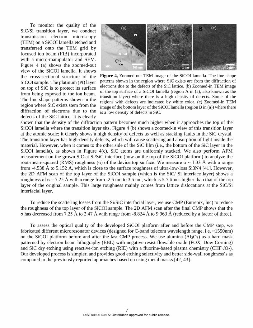
To monitor the quality of the
SiC/Si transition layer, we conduct
transmission electron microscopy
(TEM) on a SiCOI lamella etched and
transferred onto the TEM grid by
focused ion beam (FIB) incorporated
with a micro-manipulator and SEM.
Figure 4 (a) shows the zoomed-out
view of the SiCOI lamella. It shows
the cross-sectional structure of the
SiCOI sample. The platinum (Pt) layer
on top of SiC is to protect its surface
from being exposed to the ion beam.
The line-shape patterns shown in the
region where SiC exists stem from the
diffraction of electrons due to the
defects of the SiC lattice. It is clearly
shown that the density of the diffraction pattern becomes much higher when it approaches the top of the
SiCOI lamella where the transition layer sits. Figure 4 (b) shows a zoomed-in view of this transition layer
at the atomic scale; it clearly shows a high density of defects as well as stacking faults in the SiC crystal.
The transition layer has high-density defects, which will cause scattering and absorption of light inside the
material. However, when it comes to the other side of the SiC film (i.e., the bottom of the SiC layer in the
SiCOI lamella), as shown in Figure 4(c), SiC atoms are uniformly stacked. We also perform AFM
measurement on the grown SiC at Si/SiC interface (now on the top of the SiCOI platform) to analyze the
root-mean-squared (RMS) roughness (σ) of the device top surface. We measure σ ~ 1.33 Å with a range
from -4.538 Å to 5.152 Å, which is close to the surface roughness of ultra-low-loss Si3N4 [41]. However,
the 2D AFM scan of the top layer of the SiCOI sample (which is the SiC/ Si interface layer) shows a
roughness of σ = 7.25 Å with a range from -2.5 nm to 3.5 nm, which is 5-7 times higher than that of the top
layer of the original sample. This large roughness mainly comes from lattice dislocations at the SiC/Si
interfacial layer.
To reduce the scattering losses from the Si/SiC interfacial layer, we use CMP (Entrepix, Inc) to reduce
the roughness of the top layer of the SiCOI sample. The 2D AFM scan after the final CMP shows that the
σ has decreased from 7.25 Å to 2.47 Å with range from -8.824 Å to 9.963 Å (reduced by a factor of three).
To assess the optical quality of the developed SiCOI platform after and before the CMP step, we
fabricated different microresonator devices (designed for C-band telecom wavelength range, i.e. ~1550nm)
on the SiCOI platform before and after the last CMP process. We use alumina (Al2O3) as a hard mask
patterned by electron beam lithography (EBL) with negative resist flowable oxide (FOX, Dow Corning)
and SiC dry etching using reactive-ion etching (RIE) with a fluorine-based plasma chemistry (CHF3/O2).
Our developed process is simpler, and provides good etching selectivity and better side-wall roughness’s as
compared to the previously reported approaches based on using metal masks [42, 43].
Figure 4, Zoomed-out TEM image of the SiCOI lamella. The line-shape
patterns shown in the region where SiC exists are from the diffraction of
electrons due to the defects of the SiC lattice. (b) Zoomed-in TEM image
of the top surface of a SiCOI lamella (region A in (a), also known as the
transition layer) where there is a high density of defects. Some of the
regions with defects are indicated by white color. (c) Zoomed-in TEM
image of the bottom layer of the SiCOI lamella (region B in (a)) where there
is a low density of defects in SiC.
(a) (b) (c)
DISTRIBUTION A: Distribution approved for public release.
8
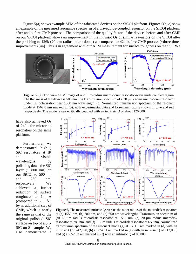
Figure 5(a) shows example SEM of the fabricated devices on the SiCOI platform. Figures 5(b, c) show
an example of the measured resonance spectru m of a waveguide-coupled resonator on the SICOI platform
after and before CMP process. The comparison of the quality factor of the devices before and after CMP
on our SiCOI platform shows an improvement in the intrinsic Qs of similar resonators on the SiCOI after
the polishing to 126k (20 µm-radius micro-donut) as compared to 42k before CMP process (~three times
improvement) [44]. This is in agreement with our AFM measurement for surface roughness on the SiC. We
have also achieved Qs
of 242k for microring
resonators on the same
platform.
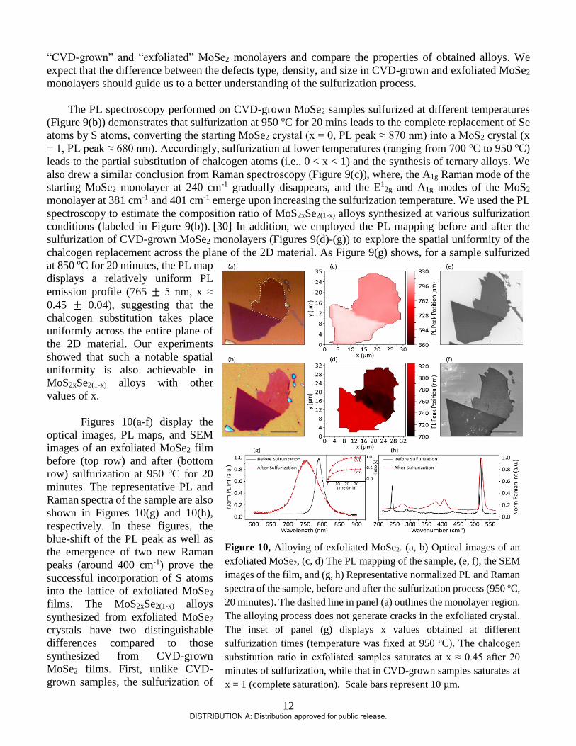
Furthermore, we
demonstrated high-Q
SiC resonators at IR
and visible
wavelengths by
polishing down the SiC
layer (~ 800 nm) on
our SiCOI to 500 nm
and 250 nm,
respectively. We
achieved a further
reduction of surface
roughness to 1.4 Å
(compared to 2.5 Å),
by an additional step of
CMP, which is nearly
the same as that of the
original polished SiC
surface on top of a 3C-
SiC-on-Si sample. We
also demonstrated a
Figure 5, (a) Top view SEM image of a 20 µm-radius micro-donut resonator-waveguide coupled region.
The thickness of the device is 500 nm. (b) Transmission spectrum of a 20 µm-radius micro-donut resonator
under TE polarization near 1550 nm wavelength. (c) Normalized transmission spectrum of the resonant
mode at 1562.0 nm marked in (b), with experimental data and Lorentzian fitting shown in blue and red,
respectively. The mode is near-critically coupled with an intrinsic Q of about 126,000.
(c) (a) (b)
Figure 6, The measured intrinsic Qs versus the outer radius of the microdisk resonators
at (a) 1550 nm, (b) 780 nm, and (c) 650 nm wavelengths. Transmission spectrum of
(d) 60-µm radius microdisk resonator at 1550 nm, (e) 20-µm radius microdisk
resonator at 780 nm, and (f) 10-µm radius microdisk resonator at 650 nm. Normalized
transmission spectrum of the resonant mode (g) at 1581.1 nm marked in (d) with an
intrinsic Q of 242,000, (h) at 774.61 nm marked in (e) with an intrinsic Q of 112,000,
and (i) at 652.52 nm marked in (f) with an intrinsic Q of 83,000.
DISTRIBUTION A: Distribution approved for public release.

9
series of microdisk resonators
working at around 1550 nm on the
500-nm thick SiC film as well as
resonators working at around 780
nm and 650 nm on the 250 nm-
thick SiC film. We demonstrated
record-high Qs of 242,000 at 1550
nm, 112,000 at 780 nm, and 83,000
at 650 nm [45] (Figure 6). These
results prove the unique
capabilities of our SiCOI platform
in form high-Q SiC resonators at a
broad wavelength range. This
platform sets the stage for the
development of high quality factor
SiC devices for nonlinear
applications at both visible and IR
wavelengths. We believe that the Q
of the resonators on the SiCOI
platform can be further improved
by starting from a thicker SiC on Si
film and removing more of the
transition SiC layer (e.g. 500 nm as
compared to 100 nm in this work) and by some adjustment in our etching process.
We also demonstrated thermally-reconfigurable high-Q SiC microring resonators with integrated
microheaters on a 3C-SiCOI platform. This platform offers an easy and reliable way for integration with
electronic devices as well as great potentials for diverse integrated optics applications. We extracted a
thermo-optic coefficient of around 2.67×10⁻⁵ /K for 3C-SiC from wavelength shift of a resonator heated by
a hot plate. Finally, we fabricateed a 40 µm-radius microring resonator with intrinsic Q of 88,000 at infrared
wavelengths (~1550 nm) after integrated with NiCr microheater. By applying current through the
microheater, a resonance shift of 30 pm/mW was achieved in the microrings, corresponding to ~50 mW per
π phase shift [46] (Figure 7). We have also designed more efficient and fast thermally reconfigured SiC
structures, which will be tested soon, that take advantage of the high thermal conductivity of SiC to achieve
very fast reconfiguration times (< 100’s ns) and considerably lower power consumptions, by directly
integrating the heater on the SiC devices. Along with the thermally tunable SiC devices, we also have
designed SiC reconfigurable devices based on carrier accumulation for much ultra-fast and low- power
reconfigurable devices, in expense of slightly higher loss, and lower tuning dynamic range.
II.C. Heterostructures in 2D TMDCs as a promising platform for nonlinear photonic devices As it was explained in the last annual report, 2D TMDCs provide specific advantages that make them a
great alternative for demonstration of fast and efficient nonlinear photonic devices. The fast carrier
dynamics of TMDCs along with their strong interaction with light and their high sensitivity of their effective
refractive index to modulation of carrier density enable efficient all-optical nonlinear processing based on
both second-order and third–order nonlinearities. Our focus on development of nonlinear photonic
structures based on 2D MDCs has been based on developing in-plane (i.e., lateral) 2D TDMC
heterostructures (e.g. lateral quantum dots and quantum wells), which we expect to greatly enhance the
nonlinear optical properties of the 2D TMDCs. We have developed a technique for selective area 2D TMDC
composition modulation, which enables us to locally engineer the 2D TMDC material band structures and
Figure 7, (a) The optical micrograph of microring resonator with the
integration of microheater. Insets are the zoomed-in SEM image of the
coupling region of the device and its transmission spectra showing an
intrinsic Q of 88,000. (b) The experimentally measured transmission spectra
of the microring resonator and (c) the numerical and experimental results of
the resonance wavelength shift with different power dissipations.
(a)
(b)
(c)
DISTRIBUTION A: Distribution approved for public release.

10
design heterostructures with the desired profile. In the last annual report, we reported our achievement on
development of ternary 2D TMDCs (MSxSe2-x) alloys with desired composition through the sulfurization
of selenide-based TMDCs (i.e., MSe2) as well as our effort on development of heterostructures based on
lithography-defined (E-beam lithography) selective masking of the TMDCs during the sulfurization
process. We also reported the issue of the crack formation in the converted (i.e., composition modulated)
TMDC caused by the conversion-induced strain. Following this effort, we have carefully studied the
fundamental causes of the crack formation and found the relation of the defects in the initial TMDC (here
MoSe2) monolayers on the crack-formation process. Furthermore, we used an arsenal of different
characterization techniques (e.g., Raman, Low-temperature photoluminescence (PL), and scanning
transmission-electron microscopy (STEM)) along with theoretical studies based on density function theory
(DFT) to study the conversion process. By studying the difference between the conversion process in the
CVD (chemical vapor deposition)-deposited and exfoliated monolayers MoSe2 samples (with different
growth condition), we found that the defects play an important role in the conversion process. This not only
provides a better understanding of the process for the development of the 2D TMDC heterostructures, but
enables us to use defect engineering as a tool to achieve a better control over the composition and the
geometry of the designed TMDC heterostructure devices.
II.C.1. Overview of the TMDC alloying and heterostructure development
Alloying of TMDCs has long served as a key technique for tuning their optoelectronic properties [47, 48].
Indeed, in ternary TMD alloys (i.e., MX’2xX2(1-x) or M’xM1-xX2; M, M’: transition metals and X, X’:
chalcogens), tuning the composition ratio (i.e., x) enables customizing the bandgap of 2D materials, offering
specifications that binary crystals (i.e., MX2) fail to provide. In addition to the rudimentary bandgap tuning,
alloying methods based on the post-growth composition modulation of binary crystals have found unique
applications in the synthesis of lateral heterostructures with arbitrary shapes and dimensions [49, 50].
Our two-step alloying approach employs a standard CVD method for synthesis of monolayer TMDC
composed of metal M and chalcogen X
(e.g., MoSe2 crystals) (first step)
followed by a high temperature
exposure to a different chalcogen (X’)
to incorporate foreign atoms (e.g., S)
into the host lattice of the MX2. The
chalcogen substitution (i.e.,
sulfurization or selenization) step is
done using a high-temperature
annealing process under a chalcogen
vapor ambient in a dedicated furnace
[51]. The degree of the sulfurization
can be controlled by adjusting
sulfurization process temperature and
time to achieve alloys with different
stoichiometry (Figure 8(a)).
The SEM inspection of several
independently converted samples
consistently confirms that more than ~
90 % of the converted MoS2 monolayer
crystals are entirely cracked (Figure
8(b)). The formation of the cracks can
Figure 8, (a) (b) PL spectroscopy representing continuous tuning of the
light emission energy (or the bandgap) between individual emission lines
corresponding to pristine MoS2 and MoSe2. Similar tuning effect can be
observed via Raman spectroscopy. (b) Crack formation in converted MoS2
monolayer crystals (SEM of an entirely cracked flake). (c,d) Experimental
demonstration of the lithography-assisted approach for fabrication of lateral
heterostructures (e.g., MoS2-MoSe2); (c) optical image of the structure and
(d) Raman measurements across the line shown in (c).
(a) (b)
(c) (d)
DISTRIBUTION A: Distribution approved for public release.

11
be attributed to the post-alloying strain caused by lattice constant mismatch between MoS2 and MoSe2 and
the thermal-expansion (in the high temperature conversion process) (leading to a total stress of 4% to 5%)
along with the reduces critical strain of MoS2 (down from 11% to less than 4%) by the pre-existing
defects/cracks in the initial 2D material (and those generated during the conversation process). The
calculations based on Griffith method [52] show that defect sizes in the range of 1 nm (corresponding to a
few atom vacancies) can lead to cracks with strains as low as 4%. Our initial TEM study of the MoSe2
samples show that the initial CVD MoSe2 has a relatively high density of such defects. In the next section,
we will explain how this challenge can be addressed.
We have also developed an alternative lithography-assisted approach for the realization of lateral
heterostructures based on selective compositions modulation. In this approach, using standard lithography
techniques combined with deposition methods (e.g., e-beam evaporation), parts of a pre-grown 2D TMDC
film are protected with a mask and unprotected regions are selectively converted into a different 2D material
(using the indirect alloying method explained in previous sections). Our experimental results demonstrate
the possibility of achieving lateral MoSe2/MoS2 HSs based on selective area composition modulation of a
pre-grown MoSe2 crystal (Figure 8(c, d)). The proposed lithography-based approach enables to
deterministically form lateral heterostructures with intended lateral dimensions and position. These features
are essential for integration of 2D heterostructures in hybrid optoelectronic devices using mainstream
CMOS fabrication processes. Moreover, the application of nanolithography techniques (e.g., EBL) enables
to fabricate quantum-confined lateral heterostructures with fine feature sizes (< 10 nm).
II.C.2. Fundamental study of the role of the defects in the development of 2D TMDC alloys and
heterostructures
Despite the diverse extent of
current studies, the role of native
defects in the alloying of
monolayer TMDCs has remained
largely unexplored. In the
post-growth alloying approach,
the presence of native defects in
the starting host crystal may
affect the details of the alloying
process as well as the ultimate
properties of ternary crystals
synthesized via the post-growth
alloying approach. Since we
synthesize MoS2xSe2(1-x) films
using the post-growth alloying
method, the quality of starting
MoSe2 films has a significant
influence on the obtained
properties of alloys as well as on
required sulfurization
parameters.
To study the effect of the
defects on the conversion
process, we perform our
sulfurization process on both
Figure 9, Synthesis of 2D ternary alloys via the chalcogen substitution. (a)
Schematic representation of the alloying process. (b, c) Representative PL
and Raman spectra, respectively, acquired from CVD-grown MoSe2
monolayers sulfurized at various temperatures for 20 mins. Composition
ratios (i.e., x) are marked on the PL spectra in (b). (d, e) The optical-
microscope images and (f, g) PL maps of a representative monolayer film
before and after sulfurization (850 oC, 20 mins), respectively. (h) The SEM
image of the MoSe2 film before sulfurization. (i) The SEM image taken from
the bottom-right corner of the triangle after the sulfurization.
DISTRIBUTION A: Distribution approved for public release.
12
“CVD-grown” and “exfoliated” MoSe2 monolayers and compare the properties of obtained alloys. We
expect that the difference between the defects type, density, and size in CVD-grown and exfoliated MoSe2
monolayers should guide us to a better understanding of the sulfurization process.
The PL spectroscopy performed on CVD-grown MoSe2 samples sulfurized at different temperatures
(Figure 9(b)) demonstrates that sulfurization at 950 oC for 20 mins leads to the complete replacement of Se
atoms by S atoms, converting the starting MoSe2 crystal (x = 0, PL peak ≈ 870 nm) into a MoS2 crystal (x
= 1, PL peak ≈ 680 nm). Accordingly, sulfurization at lower temperatures (ranging from 700 oC to 950 oC)
leads to the partial substitution of chalcogen atoms (i.e., 0 < x < 1) and the synthesis of ternary alloys. We
also drew a similar conclusion from Raman spectroscopy (Figure 9(c)), where, the A1g Raman mode of the
starting MoSe2 monolayer at 240 cm-1 gradually disappears, and the E12g and A1g modes of the MoS2
monolayer at 381 cm-1 and 401 cm-1 emerge upon increasing the sulfurization temperature. We used the PL
spectroscopy to estimate the composition ratio of MoS2xSe2(1-x) alloys synthesized at various sulfurization
conditions (labeled in Figure 9(b)). [30] In addition, we employed the PL mapping before and after the
sulfurization of CVD-grown MoSe2 monolayers (Figures 9(d)-(g)) to explore the spatial uniformity of the
chalcogen replacement across the plane of the 2D material. As Figure 9(g) shows, for a sample sulfurized
at 850 oC for 20 minutes, the PL map
displays a relatively uniform PL
emission profile (765 ± 5 nm, x ≈
0.45 ± 0.04), suggesting that the
chalcogen substitution takes place
uniformly across the entire plane of
the 2D material. Our experiments
showed that such a notable spatial
uniformity is also achievable in
MoS2xSe2(1-x) alloys with other
values of x.
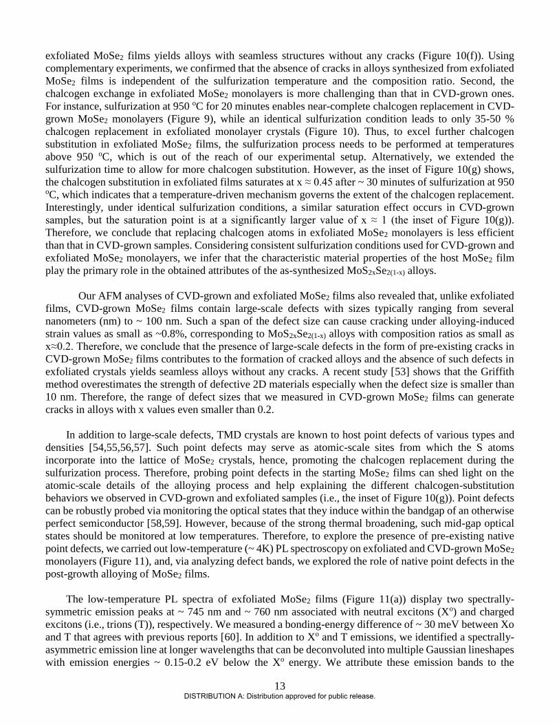
Figures 10(a-f) display the
optical images, PL maps, and SEM
images of an exfoliated MoSe2 film
before (top row) and after (bottom
row) sulfurization at 950 oC for 20
minutes. The representative PL and
Raman spectra of the sample are also
shown in Figures 10(g) and 10(h),
respectively. In these figures, the
blue-shift of the PL peak as well as
the emergence of two new Raman
peaks (around 400 cm-1) prove the
successful incorporation of S atoms
into the lattice of exfoliated MoSe2
films. The MoS2xSe2(1-x) alloys
synthesized from exfoliated MoSe2
crystals have two distinguishable
differences compared to those
synthesized from CVD-grown
MoSe2 films. First, unlike CVD-
grown samples, the sulfurization of
Figure 10, Alloying of exfoliated MoSe2. (a, b) Optical images of an
exfoliated MoSe2, (c, d) The PL mapping of the sample, (e, f), the SEM
images of the film, and (g, h) Representative normalized PL and Raman
spectra of the sample, before and after the sulfurization process (950 oC,
20 minutes). The dashed line in panel (a) outlines the monolayer region.
The alloying process does not generate cracks in the exfoliated crystal.
The inset of panel (g) displays x values obtained at different
sulfurization times (temperature was fixed at 950 oC). The chalcogen
substitution ratio in exfoliated samples saturates at x ≈ 0.45 after 20
minutes of sulfurization, while that in CVD-grown samples saturates at
x = 1 (complete saturation). Scale bars represent 10 µm.
DISTRIBUTION A: Distribution approved for public release.
13
exfoliated MoSe2 films yields alloys with seamless structures without any cracks (Figure 10(f)). Using
complementary experiments, we confirmed that the absence of cracks in alloys synthesized from exfoliated
MoSe2 films is independent of the sulfurization temperature and the composition ratio. Second, the
chalcogen exchange in exfoliated MoSe2 monolayers is more challenging than that in CVD-grown ones.
For instance, sulfurization at 950 oC for 20 minutes enables near-complete chalcogen replacement in CVD-
grown MoSe2 monolayers (Figure 9), while an identical sulfurization condition leads to only 35-50 %
chalcogen replacement in exfoliated monolayer crystals (Figure 10). Thus, to excel further chalcogen
substitution in exfoliated MoSe2 films, the sulfurization process needs to be performed at temperatures
above 950 oC, which is out of the reach of our experimental setup. Alternatively, we extended the
sulfurization time to allow for more chalcogen substitution. However, as the inset of Figure 10(g) shows,
the chalcogen substitution in exfoliated films saturates at x ≈ 0.45 after ~ 30 minutes of sulfurization at 950 oC, which indicates that a temperature-driven mechanism governs the extent of the chalcogen replacement.
Interestingly, under identical sulfurization conditions, a similar saturation effect occurs in CVD-grown
samples, but the saturation point is at a significantly larger value of x ≈ 1 (the inset of Figure 10(g)).
Therefore, we conclude that replacing chalcogen atoms in exfoliated MoSe2 monolayers is less efficient
than that in CVD-grown samples. Considering consistent sulfurization conditions used for CVD-grown and
exfoliated MoSe2 monolayers, we infer that the characteristic material properties of the host MoSe2 film
play the primary role in the obtained attributes of the as-synthesized MoS2xSe2(1-x) alloys.
Our AFM analyses of CVD-grown and exfoliated MoSe2 films also revealed that, unlike exfoliated
films, CVD-grown MoSe2 films contain large-scale defects with sizes typically ranging from several
nanometers (nm) to ~ 100 nm. Such a span of the defect size can cause cracking under alloying-induced
strain values as small as ~0.8%, corresponding to MoS2xSe2(1-x) alloys with composition ratios as small as
x≈0.2. Therefore, we conclude that the presence of large-scale defects in the form of pre-existing cracks in
CVD-grown MoSe2 films contributes to the formation of cracked alloys and the absence of such defects in
exfoliated crystals yields seamless alloys without any cracks. A recent study [53] shows that the Griffith
method overestimates the strength of defective 2D materials especially when the defect size is smaller than
10 nm. Therefore, the range of defect sizes that we measured in CVD-grown MoSe2 films can generate
cracks in alloys with x values even smaller than 0.2.
In addition to large-scale defects, TMD crystals are known to host point defects of various types and
densities [54,55,56,57]. Such point defects may serve as atomic-scale sites from which the S atoms
incorporate into the lattice of MoSe2 crystals, hence, promoting the chalcogen replacement during the
sulfurization process. Therefore, probing point defects in the starting MoSe2 films can shed light on the
atomic-scale details of the alloying process and help explaining the different chalcogen-substitution
behaviors we observed in CVD-grown and exfoliated samples (i.e., the inset of Figure 10(g)). Point defects
can be robustly probed via monitoring the optical states that they induce within the bandgap of an otherwise
perfect semiconductor [58,59]. However, because of the strong thermal broadening, such mid-gap optical
states should be monitored at low temperatures. Therefore, to explore the presence of pre-existing native
point defects, we carried out low-temperature (~ 4K) PL spectroscopy on exfoliated and CVD-grown MoSe2
monolayers (Figure 11), and, via analyzing defect bands, we explored the role of native point defects in the
post-growth alloying of MoSe2 films.
The low-temperature PL spectra of exfoliated MoSe2 films (Figure 11(a)) display two spectrally-
symmetric emission peaks at ~ 745 nm and ~ 760 nm associated with neutral excitons (Xo) and charged
excitons (i.e., trions (T)), respectively. We measured a bonding-energy difference of ~ 30 meV between Xo
and T that agrees with previous reports [60]. In addition to Xo and T emissions, we identified a spectrally-
asymmetric emission line at longer wavelengths that can be deconvoluted into multiple Gaussian lineshapes
with emission energies ~ 0.15-0.2 eV below the Xo energy. We attribute these emission bands to the
DISTRIBUTION A: Distribution approved for public release.
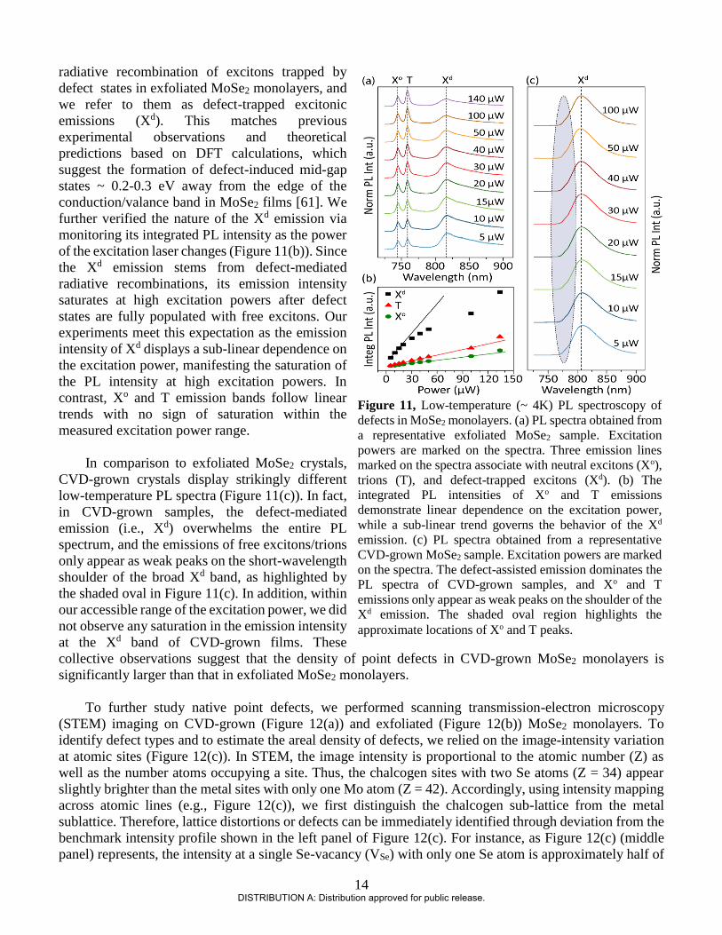
14
radiative recombination of excitons trapped by
defect states in exfoliated MoSe2 monolayers, and
we refer to them as defect-trapped excitonic
emissions (Xd). This matches previous
experimental observations and theoretical
predictions based on DFT calculations, which
suggest the formation of defect-induced mid-gap
states ~ 0.2-0.3 eV away from the edge of the
conduction/valance band in MoSe2 films [61]. We
further verified the nature of the Xd emission via
monitoring its integrated PL intensity as the power
of the excitation laser changes (Figure 11(b)). Since
the Xd emission stems from defect-mediated
radiative recombinations, its emission intensity
saturates at high excitation powers after defect
states are fully populated with free excitons. Our
experiments meet this expectation as the emission
intensity of Xd displays a sub-linear dependence on
the excitation power, manifesting the saturation of
the PL intensity at high excitation powers. In
contrast, Xo and T emission bands follow linear
trends with no sign of saturation within the
measured excitation power range.
In comparison to exfoliated MoSe2 crystals,
CVD-grown crystals display strikingly different
low-temperature PL spectra (Figure 11(c)). In fact,
in CVD-grown samples, the defect-mediated
emission (i.e., Xd) overwhelms the entire PL
spectrum, and the emissions of free excitons/trions
only appear as weak peaks on the short-wavelength
shoulder of the broad Xd band, as highlighted by
the shaded oval in Figure 11(c). In addition, within
our accessible range of the excitation power, we did
not observe any saturation in the emission intensity
at the Xd band of CVD-grown films. These
collective observations suggest that the density of point defects in CVD-grown MoSe2 monolayers is
significantly larger than that in exfoliated MoSe2 monolayers.
To further study native point defects, we performed scanning transmission-electron microscopy
(STEM) imaging on CVD-grown (Figure 12(a)) and exfoliated (Figure 12(b)) MoSe2 monolayers. To
identify defect types and to estimate the areal density of defects, we relied on the image-intensity variation
at atomic sites (Figure 12(c)). In STEM, the image intensity is proportional to the atomic number (Z) as
well as the number atoms occupying a site. Thus, the chalcogen sites with two Se atoms (Z = 34) appear
slightly brighter than the metal sites with only one Mo atom (Z = 42). Accordingly, using intensity mapping
across atomic lines (e.g., Figure 12(c)), we first distinguish the chalcogen sub-lattice from the metal
sublattice. Therefore, lattice distortions or defects can be immediately identified through deviation from the
benchmark intensity profile shown in the left panel of Figure 12(c). For instance, as Figure 12(c) (middle
panel) represents, the intensity at a single Se-vacancy (VSe) with only one Se atom is approximately half of
Figure 11, Low-temperature (~ 4K) PL spectroscopy of
defects in MoSe2 monolayers. (a) PL spectra obtained from
a representative exfoliated MoSe2 sample. Excitation
powers are marked on the spectra. Three emission lines
marked on the spectra associate with neutral excitons (Xo),
trions (T), and defect-trapped excitons (Xd). (b) The
integrated PL intensities of Xo and T emissions
demonstrate linear dependence on the excitation power,
while a sub-linear trend governs the behavior of the Xd
emission. (c) PL spectra obtained from a representative
CVD-grown MoSe2 sample. Excitation powers are marked
on the spectra. The defect-assisted emission dominates the
PL spectra of CVD-grown samples, and Xo and T
emissions only appear as weak peaks on the shoulder of the
Xd emission. The shaded oval region highlights the
approximate locations of Xo and T peaks.
DISTRIBUTION A: Distribution approved for public release.

15
the intensity at a chalcogen site
that is occupied by two Se atoms,
and the intensity at a double-Se
vacancy (V2Se) drops to the
background level because there is
no Se atom at such atomic sites.
Using this criterion, we analyzed
STEM images and concluded
that the VSe vacancy is the
dominant defect type in both
CVD-grown and exfoliated
MoSe2 films. In addition to VSe
vacancies, CVD-grown MoSe2
films also host V2Se vacancies at
a relatively lower density. We did
not observe other types of point
defects or any extended defects
in either MoSe2 samples.
Using the above criterion,
we can count the number of VSe
and V2Se vacancies across an
imaged area, and we estimated
the areal density of vacancies in
CVD-grown and exfoliated films. Inspecting several samples from each MoSe2 type showed that the average
density of VSe vacancies in CVD-grown and exfoliated films are ~ 1.23×106 µm-2 and ~ 0.42×106 µm-2,
respectively. We also estimated a density of ~ 0.11×106 µm-2 for V2Se vacancies in CVD-grown monolayers.
These estimated areal vacancy densities translate into 7.83% and 2.17% Se deficiencies in CVD-grown and
exfoliated monolayers, respectively. Indeed, the Se deficiency in CVD-grown films is more than three times
larger than that in exfoliated MoSe2 monolayers. Since our alloying approach relies on replacing Se atoms
by S atoms, the unoccupied Se sites (i.e., Se vacancies) in starting MoSe2 crystals may serve as atomic sites
from which S atoms enter the MoSe2 lattice. Thus, we speculate that the presence of Se vacancies lowers
the barrier for the chalcogen substitution and mediates the alloying process. Accordingly, the sulfurization
of CVD-grown MoSe2 films with abundant Se vacancies results in MoS2xSe2(1-x) alloys with x values larger
than that in exfoliated samples with fewer native Se vacancies.
To obtain further insight into the defect-mediated alloying mechanism, we collaborated with Reed’s
group at Stanford University to performed density-functional theory (DFT) calculations. In our DFT studies,
we consider that S atoms may incorporate into the host lattice of MoSe2 via occupying the pre-existing
vacancy sites, which may serve as niches from which the alloying process initiates and further spreads
throughout the lattice (Figure 13). However, our STEM analysis showed that the Se deficiency in host
MoSe2 monolayers is limited to only 7.83% (in CVD-grown samples). Thus, a sustainable defect-mediated
alloying process needs further generation of Se vacancies after the pre-existing vacancies are occupied by
S atoms. Our calculations show that the energy barrier for the generation of Se vacancies is larger than the
thermal energy provided during the high-temperature alloying process (i.e., KT ≈ 0.12 eV @ 950 ̊C),
meaning that the thermal desorption of Se atoms is unlikely. However, our DFT calculations suggest that
such an energy barrier can be supplied by the energy released upon the occupation of pre-existing Se
vacancies by S atoms, which enables the chalcogen substitution to proceed beyond the level of pre-existing
Se deficiencies.
Figure 12, STEM analysis of native point defects. (a,b) High-resolution
STEM images of representative CVD-grown and exfoliated MoSe2 monolayer
films, respectively. Red and blue circles mark Mo and Se2 atomic sites,
respectively. (c) Intensity profiles across the atomic lines highlighted in (a)
and (b). Identical color codes are used in panels (a-c). Using the intensity
profile (left profile), the Mo sublattice can be distinguished from the Se2 sub-
lattice. Accordingly, deviation from the reference intensities is used to identify
vacancies on CVD-grown (middle profile) and exfoliated (right profile)
MoSe2 sample. A few representative VSe and V2Se vacancies are marked on
the STEM images.
DISTRIBUTION A: Distribution approved for public release.
16
As demonstrated in PL maps, our
sulfurization process yields
MoS2xSe2(1-x) alloys with spatially
uniform compositions across the whole
plane of 2D material, suggesting that a
diffusion process assists the uniform
distribution of S atoms within the plane
of host MoSe2 monolayers. To
computationally study this
phenomenon, we considered (in
collaboration with E. Reed at Stanford
University) a two-step process in
which a sulfur binds to a Se-vacancy
site and then diffuses throughout the
layer via exchanging position with Se
vacancies. To estimate an energy
barrier for this process, we performed
nudged elastic band (NEB)
calculations using DFT calculations
[62]. Our estimation indicates that S
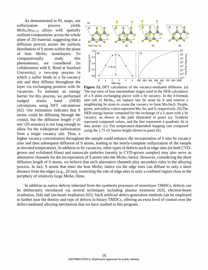
atoms could be diffusing through the
crystal, but the diffusion length (~20
nm/√20 minutes) is not long enough to
allow for the widespread sulfurization
from a single vacancy site. Thus, a
higher vacancy concentration throughout the sample could enhance the incorporation of S into Se vacancy
sites and then subsequent diffusion of S atoms, leading to the nearly-complete sulfurization of the sample
at elevated temperatures. In addition to Se vacancies, other types of defects such as edge sites (in both CVD-
grown and exfoliated films) and nanoscale pinholes (mostly in CVD-grown samples) may also serve as
alternative channels for the incorporation of S atoms into the MoSe2 lattice. However, considering the short
diffusion length of S atoms, we believe that such alternative channels play secondary roles in the alloying
process. In fact, S atoms that enter the host MoSe2 lattice via the edge sites can diffuse to only a short
distance from the edges (e.g., 20 nm), restricting the role of edge sites to only a confined region close to the
periphery of relatively large MoSe2 films.
In addition to native defects inherited from the synthesis processes of monolayer TMDCs, defects can
be deliberately introduced via several techniques including plasma treatment [63], electron-beam
irradiation, [64] and ion-beam irradiation [65]. Such artificial defect-generation methods can be employed
to further tune the density and type of defects in binary TMDCs, offering an extra level of control over the
defect-mediated alloying mechanism that we have studied in this program.
Figure 13, DFT calculation of the vacancy-mediated diffusion. (a)
The top view of four intermediate stages used in the NEB calculation
of a S atom exchanging places with a Se vacancy. In the 4-formula
unit cell of MoSe2, we replace one Se atom by S and remove a
neighboring Se atom to create the vacancy to form Mo4Se6S. Purple,
green, and yellow colors represent Mo, Se, and S, respectively. (b) The
NEB energy barrier computed for the exchange of a S atom with a Se
vacancy, as shown in the path illustrated in panel (a). Symbols
represent computed values, and the line represents a quadratic fit to
data points. (c) The temperature-dependent hopping rate computed
using the 1.75 eV barrier height shown in panel (b).
DISTRIBUTION A: Distribution approved for public release.

17
III. Publications and Presentations
III.A. Journal papers
2018
[1] A. E. Dorche, A. H. Hosseinnia, A. A. Eftekhar, and A. Adibi, “Wideband bright-soliton frequency-
comb generation at optical telecommunication wavelength in a thin silicon nitride film,” Journal of
Nanophotonics, vol. 12, no. 4, pp. 046008, 2018.
[2] T. Fan, H. Moradinejad, X. Wu, A. A. Eftekhar, and A. Adibi, “High-Q integrated photonic
microresonators on 3c-sic-on-insulator (sicoi) platform,” Optics express, vol. 26, no. 20, pp. 25814-25826,
2018.
[3] S. H. S. Mousavi, R. Lemasters, F. Wang, A. E. Dorche, H. Taheri, A. A. Eftekhar, H. Harutyunyan,
and A. Adibi, “Phase-matched nonlinear second-harmonic generation in plasmonic metasurfaces,”
Nanophotonics, 2019.
[4] H. Taghinejad, A. A. Eftekhar, P. M. Campbell, B. Beatty, M. Taghinejad, Y. Zhou, C. J. Perini, H.
Moradinejad, W. E. Henderson, and E. V. Woods, “Strain relaxation via formation of cracks in
compositionally modulated two-dimensional semiconductor alloys,” npj 2D Materials and Applications,
vol. 2, 2018.
[5] H. Taghinejad, D. A. Rehn, C. Muccianti, A. A. Eftekhar, M. Tian, T. Fan, X. Zhang, Y. Meng, Y.
Chen, and T.-V. Nguyen, “Defect-mediated alloying of monolayer transition-metal dichalcogenides,” ACS
nano, vol. 12, no. 12, pp. 12795-12804, 2018.
[6] M. Taghinejad, H. Taghinejad, S. T. Malak, H. Moradinejad, E. V. Woods, Z. Xu, Y. Liu, A. A.
Eftekhar, T. Lian, and V. V. Tsukruk, “Sharp and tunable crystal/fano‐type resonances enabled by out‐of‐
plane dipolar coupling in plasmonic nanopatch arrays,” Annalen der Physik, vol. 530, no. 10, pp. 1700395,
2018.
[7] M. Taghinejad, H. Taghinejad, Z. Xu, K.-T. Lee, S. P. Rodrigues, J. Yan, A. Adibi, T. Lian, and W.
Cai, “Ultrafast control of phase and polarization of light expedited by hot-electron transfer,” Nano letters,
vol. 18, no. 9, pp. 5544-5551, 2018.
[8] M. Taghinejad, H. Taghinejad, Z. Xu, Y. Liu, S. P. Rodrigues, K. T. Lee, T. Lian, A. Adibi, and W.
Cai, “Hot‐electron‐assisted femtosecond all‐optical modulation in plasmonics,” Advanced Materials, vol.
30, no. 9, pp. 1704915, 2018.
[9] Hossein Taghinejad, Ali A. Eftekhar, Ali Adibi, “Lateral and Vertical Heterostructures in Two-
dimensional Transition-Metal Dichalcogenides,” Invited review, Optics material express
Previous years
[10] H. Taghinejad, M. Taghinejad, A. Tarasov, M. Y. Tsai, A. H. Hosseinnia, H. Moradinejad, P. M.
Campbell, A. A. Eftekhar, E. M. Vogel, A. Adibi “Resonant light-induced heating in hybrid cavity-coupled
2D transition-metal dichalcogenides,” ACS Photonics, 3 (4), pp. 700-707, 2016.
[11] H. Taghinejad, S. H. Shams-Mousavi, Y. Gong, M. Taghinejad, A. A Eftekhar, P. Ajayan, A. Adibi
“Lattice plasmon induced large enhancement of excitonic emission in monolayer metal
dichalcogenides,” Plasmonics, pp.1-7, 2017.
[12] H. Taheri, A. A. Eftekhar, K. Wiesenfeld, and A. Adibi, “Anatomy of phase locking in hyperparametric
oscillations based on kerr nonlinearity,” IEEE Photonics Journal, 9(3), pp.1-11, 2017.
DISTRIBUTION A: Distribution approved for public release.

18
[13] H. Taheri, P. Del'Haye, A. A. Eftekhar, K. Wiesenfeld, and A. Adibi, “Self-synchronization phenomena
in the Lugiato-Lefever equation,” Physical Review A, 96(1), p.013828, 2017.
[14] R. Dehghannasiri, M. Soltani, and A. Adibi, “Efficient finite-element formulation for analysis of
whispering-gallery-mode optical resonators,” JOSA B, 34(10), pp.2259-2265, 2017.
[15] R. Dehghannasiri, A. A. Eftekhar, and A. Adibi, “Raman-like stimulated Brillouin scattering in
phononic-crystal-assisted silicon-nitride waveguides,” Physical Review A, 96(5), p.053836, 2017.
[16] A. Eshaghian Dorche, S. Abdollahramezani, H. Taheri, A. A. Eftekhar, and A. Adibi, “Extending chip-
based Kerr-comb to visible spectrum by dispersive wave engineering,” Optics Express, vol. 25, pp. 22362-
22374, 2017.
Submitted or In-preparation Refereed Journal Papers
[17] Hesam Moradinejad, Murtaza Askari, Amir H. Atabaki, Zhixuan Xia, Ali A. Eftekhar, and Ali Adibi,
“Miniaturized High-Q Silicon Nitride Resonators at Visible Wavelengths,” Submitted to optics express
(2018).
[18] A. H. Hosseinnia, J. Lavrencik, M. Sodagar, A. A. Eftekhar, S. E. Ralph, and A. Adibi, “Integrated
Resonant Modulation in Heterogeneous Silicon on Silicon Nitride Platforms,” To be submitted to Optics
Express (2019).
[19] T. Fan, X. Wu, A. A. Eftekhar, and A. Adibi, " High-Q Microresonators at visible to IR wavelengths
on a 3C-SiC-on-Insulator Platform, “in-preparation for Optics Express.
[20] X. Wu, T. Fan, A. A. Eftekhar, and A. Adibi, “High-Q thermally reconfigurable microresonators a 3C-
SiC-on-Insulator platform,” In-preparation for Optics Letters
III.B. Refereed Conference Papers
2018
[1] R. Dehghannasiri, H. Moradinejad, T. Fan, A. H. Hosseinnia, A. A. Eftekhar, and A. Adibi, "Integrated
optomechanical resonators in double-layer crystalline silicon platforms," in 2018 IEEE Photonics
Conference (IPC), IEEE, pp. 1-2, 2018.
[2] A. E. Dorche, A. A. Eftekhar, and A. Adibi, "Kerr-comb generation in a dispersion engineered coupled
thin silicon nitride microresonators," in CLEO: QELS_Fundamental Science, Optical Society of America,
p. JTu2A. 85, 2018.
[3] A. E. Dorche, A. A. Eftekhar, and A. Adibi, "Wideband kerr-comb near visible spectrum in coupling-
engineered thin silicon nitride resonators," in CLEO: Applications and Technology, Optical Society of
America, p. JW2A. 33, 2018.
[4] T. Fan, A. A. Eftekhar, and A. Adibi, "High-q microresonators at near-infrared/near visible wavelengths
on a 3c-sic-on-insulator (sicoi) platform," in 2018 IEEE Photonics Conference (IPC), IEEE, pp. 1-2, 2018.
[5] T. Fan, H. Moradinejad, X. Wu, A. A. Eftekhar, and A. Adibi, "High Q integrated photonic
microresonators on 3c sic-on-insulator platform," in CLEO: Science and Innovations, Optical Society of
America, p. SW4A. 2, 2018.
[6] H. Taghinejad, D. Daniel Rehn, A. Eftekhar, X. Zhang, S. Shi, P. Ajayan, E. Reed, and A. Adibi, “Role
of native defects in post-synthesis alloying of transition metal dichalcogenides,” Bulletin of the American
Physical Society, 2019.
DISTRIBUTION A: Distribution approved for public release.
19
[7] H. Taghinejad, A. Eftekhar, P. Campbell, M. Taghinejad, Y. Zhou, E. Reed, E. Vogel, and A. Adibi,
"Alloying-induced biaxial strain in ternary alloys of transition-metal dichalcogenides (tmds)(conference
presentation)," in Photonic and Phononic Properties of Engineered Nanostructures VIII, International
Society for Optics and Photonics, p. 1054112, 2018.
[8] H. Taghinejad, A. Eftekhar, M. Taghinejad, Y. Zhou, E. Reed, and A. Adibi, "Crack formation induced
by the post-growth alloying of two-dimensional transition-metal dichalcogenides," in APS Meeting
Abstracts, 2018.
[9] H. Taghinejad, A. A. Eftekhar, and A. Adibi, "Lateral heterostructures in two-dimensional transition
metal dichaolcogenides for optoelectronic applications (conference presentation)," in Active Photonic
Platforms X, International Society for Optics and Photonics, p. 107210L, 2018.
[10] H. Taghinejad, A. A. Eftekhar, and A. Adibi, "Planar heterostructures through selective-area alloying
of 2d transition metal dichalcogenide (conference presentation)," in 2D Photonic Materials and Devices,
International Society for Optics and Photonics, p. 105340R, 2018.
[11] M. Taghinejad, H. Taghinejad, and A. Adibi, "Ultra-sharp and tunable lattice plasmons in film-coupled
metallic nanostructures (conference presentation)," in Photonic and Phononic Properties of Engineered
Nanostructures VIII, International Society for Optics and Photonics, p. 105410T, 2018.
[12] T. Fan, H. Taghinejad, A. H. Hosseinnia, H. Moradinejad, A. A. Eftekhar, A. Adibi, “A high-Quality
silicon nitride (SiN) platform integrated with two-dimensional (2D) materials,” SPIE OPTO. Feb 2019
[13] T. Fan, H. Moradinejad, X. Wu, A. A. Eftekhar, A. Adibi, “A 3C-SiC-on-oxide (SiCOI) platform
enabling high-Q resonators over an octave frequency range from visible to near-infrared,” SPIE OPTO. Feb
2019
Previous years
[14] R. Dehghannasiri, A. A. Eftekhar, and A. Adibi, "Raman-like stimulated Brillouin scattering in SiN
waveguides," CLEO: Science and Innovations, pp. SM1E.8, San Jose, CA, 2016.
[15] H. Taheri, P. Del'Haye, A. A. Eftekhar, K. Wiesenfeld, and A. Adibi, "Self-synchronization and phase
steps in microresonator-based optical frequency combs," CLEO: Science and Innovations, pp. STu1H.6,
San Jose, CA, 2016.
[16] H. Moradinejad, M. Askari, A. H. Atabaki, Z. Xia, A. A. Eftekhar and A. Adibi, "Miniaturized high-Q
silicon nitride resonators at visible wavelengths," IEEE Photonics Conference (IPC), Orlando, FL, 2017.
[17] R. Dehghannasiri, A. A. Eftekhar and A. Adibi, “Observation of stimulated Brillouin scattering in
Si3N4 waveguides,” IEEE Photonics Conference (IPC), Orlando, FL, 2017.
[18] A. H. Hosseinnia, M. Sodagar, H. Moradinejad, T. Fan, A. A. Eftekhar and A. Adibi, “High-speed
active devices integrated in hybrid silicon on silicon nitride platform,” Conference on Lasers and Electro-
Optics (CLEO), San Jose, CA, 2017.
[19] H. Taghinejad, M. Taghinejad, A. Tarasov, T. Fan, A. A. Eftekhar, E. M. Vogel, A. Adibi “Strong light
enhancement and confinement in two-dimensional transition metal dichalcogenides,” SPIE Photonics West,
San Francisco, CA, 2017.
[20] H. Taghinejad, M. Taghinejad, A. Tarasov, A. H. Hosseinnia, H. Moradinejad, A. A. Eftekhar, E.
Vogel, and A. Adibi, “Enhancement of light-2D material interaction envisioned for energy harvesting
applications,” Conference on Lasers and Electro-Optics (CLEO), San Jose, CA, 2017.
DISTRIBUTION A: Distribution approved for public release.

20
[21] M. Taghinejad, H. Taghinejad, H. Moradinejad, A. A. Eftekhar, and Ali Adibi, “A spectroscopic
ellipsometry demonstration of ultrasharp subradiant plasmons,” META’17 Incheon, South Korea, 2017.
[22] Fan, T., Taghinejad, H., Eftekhar, A.A. and Adibi, A. “Light-matter interaction in 2D material
heterostructures,” SPIE Photonics West Meeting, San Francisco, CA, 2017.
[23] T. Fan, H. Moradinejad, X. Wu, A. A. Eftekhar, and A. Adibi, “Crystalline silicon carbide on insulator
(SCOI) material platform for integrated photonic applications,” accepted in SPIE Photonics West, San
Francisco, CA, 2018.
[24] H. Taghinejad, A. A. Eftekhar, M. Taghinejad, and A. Adibi, “Alloying-induced biaxial strain in
ternary alloys of transition-metal dichalcogenides (TMDs),” accepted for presentation in SPIE Photonics
West, San Francisco, CA, 2018.
[25] M. Taghinejad, H. Taghinejad, and A. Adibi, “Ultra-sharp and tunable lattice plasmons in film-coupled
metallic nanostructures,” accepted for presentation in SPIE Photonics West, San Francisco, CA, 2018.
Accepted Conference Papers
[24] T. Fan, X. Wu, A. A. Eftekhar, and A. Adibi, " Record-High-Q Microresonators from 650 nm to 1550
nm Wavelengths on a 3C-SiC-on-Insulator Platform, “in CLEO: Science and Innovations, Optical Society
of America, 2019.
[25] X. Wu, T. Fan, A. A. Eftekhar, and A. Adibi, “High-Q microresonators integrated with microheaters
on a 3C-SiC-on-Insulator platform,” in CLEO: Science and Innovations, Optical Society of America, 2019.
[26] A. E. Dorche, A. A. Eftekhar, and A. Adibi, “Near-visible bright-soliton Kerr comb generation in
dispersion-engineered lithium niobate coupled optical microresonators,” in CLEO: Science and
Innovations, Optical Society of America, 2019.
III.C. Invited Presentations and Keynotes
2018
[1] A. H. Hosseinnia, N. Sodagar, H. Moradinejad, T. Fan, A. A. Eftekhar, and A. Adibi, “Hybrid Material
Platforms for Low-power, High-speed, and Miniaturized Integrated Photonic Devices and Systems.”
Invited Keynote Talk fpr presentation in Optics and Photonics Conference, Philadelphia, PA, October
2018.
[2] H. Taghinejad, A. A. Eftekhar, and A. Adibi, “Planar heterostructures through selective-area alloying of
2D transition metal dichalcogenide,” Invited for presentation in SPIE Photonics West, San Francisco, CA,
2018.
[3] H. Taghinejad, A. A. Eftekhar, A. Adibi, “Lateral heterostructures in two-dimensional transition metal
dichalcogenides for optoelectronic applications.” Invited for presentation in SPIE Optics and Photonics,
San Diego, CA, August 2018.
[4] A. H. Hosseinnia, T. Fan, H. Moradinejad, N. Sodagar, S. Taghavi, A. A. Eftekhar, and A. Adibi, “Low-
power High-speed Resonance-based Integrated Photonic Modulators.” Invited for presentation in IEEE
Photonics Conference (IPC), Reston, VA, October 2018.
[5] A. H. Hosseinnia, N. Sodagar, H. Moradinejad, T. Fan, A. A. Eftekhar, and A. Adibi, “Hybrid Material
Platforms for Reconfigurable Integrated Nanophotonics, Invited for presentation in Stegeman
Symposium.” Orlando, FL, March 2018.
DISTRIBUTION A: Distribution approved for public release.

21
[6] A. H. Hosseinnia, N. Sodagar, H. Moradinejad, T. Fan, A. A. Eftekhar, and A. Adibi, “Hybrid Material
Platforms for Low-power, High-speed, and Miniaturized Integrated Nanophotonic Devices and Systems.”
Invited seminar talk for presentation in Samsung USA, San Jose, CA, August 2018.
[7] A. Adibi, “Hybrid Material and Device Platforms for Reconfigurable Integrated Nanophotonics.”
Invited seminar talk for presentation in Georgia Tech Lorraine, Metz, France, June 2018.
[8] A. Adibi, “Hybrid Material and Device Platforms for Reconfigurable Integrated Nanophotonics.”
Invited seminar talk for presentation in Aachen University, Aachen, Germany, June 2018.
[9] A. Adibi, “Hybrid Material and Device Platforms for Reconfigurable Integrated Nanophotonics.”
Invited seminar talk for presentation in Institute of Materials for Electronics and Magnetism (IMEM-CNR),
Parma, Italy, June 2018.
[10] H. Taghinejad, “Synthesis of lateral heterostructures of transition-metal dichalcogenides via spatially-
controlled alloying,” Invited, SPIE OPTO. Feb 2019
Previous years
[11] A. Adibi, “Integrated nanophotonic structures for optical computing,” Invited for Presentation in
Beyond CMOS Computing Workshop, Baltimore, MD, February 2016.
[12] A. Adibi, “Hybrid material platforms for reconfigurable integrated photonic structures”, Invited for
Presentation in Reconfigurable Electronic Workshop, Arlington, VA, May 2016.
[13] A. H. Hosseinnia, H. Moradinejad, M. Sodagar, A. A. Eftekhar, and A. Adibi, “Hybrid CMOS-
compatible material and device platform for integrated nanophotonics,” Invited for Presentation in CLEO:
Science and Innovations, San Jose, CA, June 2016.
[14] S. H. Shams Mousavi, H. Taghinejad, M. Taghinejad, A. A. Eftekhar, and A. Adibi, “Strong light-
matter interaction in two-dimensional transition metal dichalcogenides through integration with plasmonic
nanoantenna arrays,” Invited for Presentation in META Conference, Malaga, Spain, July 2016.
[15] S. H. Shams-Mousavi, H. Taghinejad, M. Taghinejad, A. A. Eftekhar and A. Adibi, "Strong light-
matter interaction through mode engineering in plasmonic nanoantenna arrays," Invited for Presentation in
Progress in Electromagnetic Research Symposium (PIERS), Shanghai, China, July 2016.
[16] A. Adibi “Hybrid material and device platforms for reconfigurable integrated nanophotonics,” Invited
Seminar Talk, Jet Propulsion Laboratory, Pasadena, CA January 2016.
[17] A. Adibi “Hybrid material and device platforms for reconfigurable integrated nanophotonics,” Invited
Seminar Talk, University of Washington, Seattle, WA, January 2016.
[18] H. Maoradinejad, A. H. Hosseinnia, T. Fan, M. Sodagar, A. A. Eftekhar, and A. Adibi, “Hybrid multi-
layer integrated nanophotonics materials and devices,” Invited for Presentation in SPIE Optics and
Photonics, San Diego, CA, August 2016.
[19] H. Taghinejad, S. H. Shams Mousavi, T. Fan, M. Taghinejad, A. A. Eftekhar, and A. Adibi, “Plasmonic
enhancement of light-matter interaction in planar materials,” Invited for presentation in META 2017
Conference, Seoul, South Korea, 2017.
[20] H. Moradinejad, T. Fan, A. H. Hosseinnia, M. Sodagar, S. Taghavi, A. A. Eftekhar, and A. Adibi,
“Optical modulation in hybrid integrated nanophotonic platforms,” Invited for presentation in IEEE
Summer Topicals Meeting, San Juan, Puerto Rico, 2017.
DISTRIBUTION A: Distribution approved for public release.

22
References:
[1] A. E. Dorche, A. A. Eftekhar, and A. Adibi, “Near-visible bright-soliton Kerr comb generation in
dispersion-engineered lithium niobate coupled optical microresonators,” in CLEO: Science and
Innovations, Optical Society of America, 2019.
[2] A. E. Dorche, A. H. Hosseinnia, A. A. Eftekhar, and A. Adibi, “Wideband bright-soliton frequency-
comb generation at optical telecommunication wavelength in a thin silicon nitride film,” Journal of
Nanophotonics, vol. 12, no. 4, pp. 046008, 2018.
[3] T. Fan, H. Moradinejad, X. Wu, A. A. Eftekhar, and A. Adibi, “High-Q integrated photonic
microresonators on 3c-sic-on-insulator (sicoi) platform,” Optics express, vol. 26, no. 20, pp. 25814-25826,
2018.
[4] T. Fan, H. Moradinejad, X. Wu, A. A. Eftekhar, A. Adibi, “A 3C-SiC-on-oxide (SiCOI) platform
enabling high-Q resonators over an octave frequency range from visible to near-infrared,” SPIE OPTO. Feb
2019
[5] S. H. S. Mousavi, R. Lemasters, F. Wang, A. E. Dorche, H. Taheri, A. A. Eftekhar, H. Harutyunyan,
and A. Adibi, “Phase-matched nonlinear second-harmonic generation in plasmonic metasurfaces,”
Nanophotonics, 2019.
[6] M. Taghinejad, H. Taghinejad, S. T. Malak, H. Moradinejad, E. V. Woods, Z. Xu, Y. Liu, A. A. Eftekhar,
T. Lian, and V. V. Tsukruk, “Sharp and tunable crystal/fano‐type resonances enabled by out‐of‐plane
dipolar coupling in plasmonic nanopatch arrays,” Annalen der Physik, vol. 530, no. 10, pp. 1700395, 2018.
[7] M. Taghinejad, H. Taghinejad, Z. Xu, K.-T. Lee, S. P. Rodrigues, J. Yan, A. Adibi, T. Lian, and W. Cai,
“Ultrafast control of phase and polarization of light expedited by hot-electron transfer,” Nano letters, vol.
18, no. 9, pp. 5544-5551, 2018.
[8] M. Taghinejad, H. Taghinejad, Z. Xu, Y. Liu, S. P. Rodrigues, K. T. Lee, T. Lian, A. Adibi, and W. Cai,
“Hot‐electron‐assisted femtosecond all‐optical modulation in plasmonics,” Advanced Materials, vol. 30, no.
9, pp. 1704915, 2018.
[9] H. Taghinejad, A. A. Eftekhar, P. M. Campbell, B. Beatty, M. Taghinejad, Y. Zhou, C. J. Perini, H.
Moradinejad, W. E. Henderson, and E. V. Woods, “Strain relaxation via formation of cracks in
compositionally modulated two-dimensional semiconductor alloys,” npj 2D Materials and Applications,
vol. 2, 2018.
[10] H. Taghinejad, D. A. Rehn, C. Muccianti, A. A. Eftekhar, M. Tian, T. Fan, X. Zhang, Y. Meng, Y.
Chen, and T.-V. Nguyen, “Defect-mediated alloying of monolayer transition-metal dichalcogenides,” ACS
nano, vol. 12, no. 12, pp. 12795-12804, 2018.
[11] R. Dehghannasiri, H. Moradinejad, T. Fan, A. H. Hosseinnia, A. A. Eftekhar, and A. Adibi, "Integrated
optomechanical resonators in double-layer crystalline silicon platforms," in 2018 IEEE Photonics
Conference (IPC), IEEE, pp. 1-2, 2018.
[12] R. Dehghannasiri, A. A. Eftekhar and A. Adibi, “Observation of stimulated Brillouin scattering in
Si3N4 waveguides,” IEEE Photonics Conference (IPC), Orlando, FL, 2017.
[13] H. Morkoç, S. Strite, G. B. Gao, M. E. Lin, B. Sverdlov, and M. Burns, "Large-band-gap SiC, III-V
nitride, and II-VI ZnSe-based semiconductor device technologies," J. Appl. Phys. 76(3), 1363–1398 (1994).
DISTRIBUTION A: Distribution approved for public release.

23
[14] 5. R. Adair, L. L. Chase, and S. A. Payne, "Nonlinear refractive index of optical crystals," Phys. Rev.
B 39(5), 3337–3350 (1989).
[15] G. L. DesAutels, C. Brewer, M. Walker, S. Juhl, M. Finet, S. Ristich, M. Whitaker, and P. Powers,
"Femtosecond laser damage threshold and nonlinear characterization in bulk transparent SiC materials," J.
Opt. Soc. Am. B 25(1), 60-66 (2008).
[16] X. Lu, J. Y. Lee, S. Rogers, and Q. Lin, "Optical Kerr nonlinearity in a high-Q silicon carbide
microresonator," Opt. Express 22(25), 30826-30832 (2014).
[17] J. Bravo-Abad, A. Rodriguez, P. Bermel, S. G. Johnson, J. D. Joannopoulos, and M. Soljacic,
"Enhanced nonlinear optics in photonic-crystal microcavities," Opt. Express 15(24), 16161-16176 (2007).
[18] P. Del’Haye, A. Schliesser, O. Arcizet, T. Wilken, R. Holzwarth, and T. J. Kippenberg, "Optical
frequency comb generation from a monolithic microresonator," Nature 450(7173), 1214–1217 (2007).
[19]W. F. Koehl, B. B. Buckley, F. J. Heremans, G. Calusine, and D. D. Awschalom, "Room temperature
coherent control of defect spin qubits in silicon carbide," Nature 479(7371), 84–87 (2011).
[20] A. L. Falk, B. B. Buckley, G. Calusine, W. F. Koehl, V. V. Dobrovitski, A. Politi, C. A. Zorman, P. X.
L. Feng, and D. D. Awschalom, "Polytype control of spin qubits in silicon carbide," Nat. Commun. 4, 1819
(2013).
[21] S. Castelletto, B. C. Johnson, V. Ivády, N. Stavrias, T. Umeda, A. Gali, and T. Ohshima, " A silicon
carbide room-temperature single-photon source," Nat. Mater. 13, 151–156 (2013).
[22] A. Lohrmann, N. Iwamoto, Z. Bodrog, S. Castelletto, T. Ohshima, T. J. Karle, A. Gali, S. Prawer, J. C.
McCallum, and B. C. Johnson, "Single-photon emitting diode in silicon carbide," Nat. Commun. 6, 7783
(2015).
[23] H. Morkoç, S. Strite, G. B. Gao, M. E. Lin, B. Sverdlov, and M. Burns, "Large-band-gap SiC, III-V
nitride, and II-VI ZnSe-based semiconductor device technologies," J. Appl. Phys. 76(3), 1363–1398 (1994).
[24] M. Bosi, G. Attolini, M. Negri, C. Ferrari, E. Buffagni, C. Frigeri, M. Calicchio, B. Pécz, F. Riesz, I.
Cora, Z. Osváth, L. Jiang, and G. Borionetti, "Defect structure and strain reduction of 3C-SiC/Si layers
obtained with the use of a buffer layer and methyltrichlorosilane addition," Cryst. Eng. Comm. 18(15),
2770–2779 (2016).
[25] X. Lu, J. Lee, P. Feng, Q. Lin, X. Lu, J. Y. Lee, and P. X.-L. Feng," A silicon carbide microdisk
resonator," Opt. Lett. 38(8), 1304–1306 (2013).
[26] B.-S. Song, S. Yamada, T. Asano, and S. Noda, "Demonstration of two-dimensional photonic crystals
based on silicon carbide," Opt. Express 19(12), 11084-11089 (2011).
[27] S. Yamada, B. S. Song, T. Asano, and S. Noda, "Silicon carbide-based photonic crystal nanocavities
for ultra-broadband operation from infrared to visible wavelengths," Appl. Phys. Lett. 99(20), 201102
(2011).
[28] S. Yamada, B.-S. Song, T. Asano, and S. Noda, "Experimental investigation of thermo-optic effects in
SiC and Si photonic crystal nanocavities," Opt. Lett. 36(20), 3981-3983 (2011).
[29] S. Yamada, B. Song, J. Upham, T. Asano, Y. Tanaka, and S. Noda, "Suppression of multiple photon
absorption in a SiC photonic crystal nanocavity operating at 155 μm," Opt. Express 20(14), 14789-14796
(2012).
[30] J. Cardenas, M. Zhang, C. T. Phare, S. Y. Shah, C. B. Poitras, B. Guha, and M. Lipson, "High Q SiC
microresonators," Opt. Express 21(14), 16882-16887 (2013).
DISTRIBUTION A: Distribution approved for public release.

24
[31] M. Radulaski, T. M. Babinec, S. Buckley, A. Rundquist, J. Provine, K. Alassaad, G. Ferro, and J.
Vučković, "Photonic crystal cavities in cubic (3C) polytype silicon carbide films," Opt. Express 21(26),
32623-32629 (2013).
[32] A. P. Magyar, D. Bracher, J. C. Lee, I. Aharonovich, and E. L. Hu, "High quality SiC microdisk
resonators fabricated from monolithic epilayer wafers," Appl. Phys. Lett. 104(5), 051109 (2014).
[33] X. Lu, J. Y. Lee, P. X. Feng, and Q. Lin, "High Q silicon carbide microdisk resonator," Appl. Phys.
Lett. 104(18), 181103 (2014).
[34] F. Martini, and A. Politi, “Linear integrated optics in 3C silicon carbide,” Opt. Express 25(10), 10735-
10742 (2017).
[35] L. D. Cioccio, F. Letertre, Y. L. Tiec, A. M. Papon, C. Jaussaud, and M. Bruel, "Silicon carbide on
insulator formation by the Smart-Cut process," Mater. Sci. Eng. B46(1-3), 349–356 (1997).
[36] J. Cardenas, M. Yu, Y. Okawachi, C. B. Poitras, R. K. W. Lau, A. Dutt, A. L. Gaeta, and M. Lipson,
"Optical nonlinearities in high-confinement silicon carbide waveguides," Opt. Lett. 40(17), 4138–4141
(2015).
[37] H. Moradinejad, A. H. Atabaki, A. H. Hosseinnia, A. A. Eftekhar, and A. Adibi, "Double-layer
crystalline silicon on insulator material platform for integrated photonic applications," IEEE Photonics J.
6(6), 1-8 (2014).
[38] A. H. Hosseinnia, A. H. Atabaki, A. A. Eftekhar, and A. Adibi, "High-quality silicon on silicon nitride
integrated optical platform with an octave-spanning adiabatic interlayer coupler," Opt. Express 23(23),
30297-30307 (2015).
[39] T. Fan, X. Wu, A. A. Eftekhar, and A. Adibi, " Record-High-Q Microresonators from 650 nm to 1550
nm Wavelengths on a 3C-SiC-on-Insulator Platform," in CLEO: Science and Innovations, Optical Society
of America, 2019.
[40] M. Bosi, C. Ferrari, D. Nilsson, and P. J. Ward, "3C-SiC carbonization optimization and void reduction
on misoriented Si substrates: from a research reactor to a production scale reactor," Cryst. Eng. Comm.
18(39), 7478–7486 (2016).
[41] X. Ji, F. A. S. Barbosa, S. P. Roberts, A. Dutt, J. Cardenas, Y. Okawachi, A. Bryant, A. L. Gaeta, and
M. Lipson, "Ultra-low-loss on-chip resonators with sub-milliwatt parametric oscillation threshold," Optica
4(6), 619-624 (2017).
[42] J. Cardenas, M. Zhang, C. T. Phare, S. Y. Shah, C. B. Poitras, B. Guha, and M. Lipson, "High Q SiC
microresonators," Opt. Express 21(14), 16882-16887 (2013).
[43] X. Lu, J. Y. Lee, P. X. Feng, and Q. Lin, "High Q silicon carbide microdisk resonator," Appl. Phys.
Lett. 104(18), 181103 (2014).
[44] T. Fan, H. Moradinejad, X. Wu, A. A. Eftekhar, and A. Adibi, “High-Q integrated photonic
microresonators on 3C-SiC-on-insulator (SiCOI) platform,” Optics express, vol. 26, no. 20, pp. 25814-
25826, 2018.
[45] T. Fan, X. Wu, A. A. Eftekhar, and A. Adibi, " Record-High-Q Microresonators from 650 nm to 1550
nm Wavelengths on a 3C-SiC-on-Insulator Platform," in CLEO: Science and Innovations, Optical Society
of America, 2019.
[46] X. Wu, T. Fan, A. A. Eftekhar, and A. Adibi, “High-Q microresonators integrated with microheaters
on a 3C-SiC-on-Insulator platform,” in CLEO: Science and Innovations, Optical Society of America, 2019.
DISTRIBUTION A: Distribution approved for public release.
25
[47] Duan, X. D.; Wang, C.; Fan, Z.; Hao, G. L.; Kou, L. Z.; Halim, U.; Li, H. L.; Wu, X. P.; Wang, Y. C.;
Jiang, J. H.; Pan, A. L.; Huang, Y.; Yu, R. Q.; Duan, X. F. Synthesis of WS2xSe2-2x Alloy Nanosheets with
Composition-Tunable Electronic Properties. Nano Lett 2016, 16, 264-269..
[48] Li, H. L.; Duan, X. D.; Wu, X. P.; Zhuang, X. J.; Zhou, H.; Zhang, Q. L.; Zhu, X. L.; Hu, W.; Ren, P.
Y.; Guo, P. F.; Ma, L.; Fan, X. P.; Wang, X. X.; Xu, J. Y.; Pan, A. L.; Duan, X. F. Growth of Alloy
MoS2xSe2(1-x) Nanosheets with Fully Tunable Chemical Compositions and Optical Properties. J Am Chem
Soc 2014, 136, 3756-3759
[49] Mahjouri-Samani, M.; Lin, M. W.; Wang, K.; Lupini, A. R.; Lee, J.; Basile, L.; Boulesbaa, A.; Rouleau,
C. M.; Puretzky, A. A.; Ivanov, I. N.; Xiao, K.; Yoon, M.; Geohegan, D. B. Patterned Arrays of Lateral
Heterojunctions Within Monolayer Two-Dimensional Semiconductors. Nat Commun 2015, 6, 7749.
[50] Taghinejad, H.; Eftekhar, A. A.; Campbell, P. M.; Beatty, B.; Taghinejad, M.; Zhou, Y.; Perini, C. J.;
Moradinejad, H.; Henderson, W. E.; Woods, E. V.; Zhang, Z.; Ajayan, P. M.; Reed, E. J.; Vogel, E. M.;
Adibi, A. Strain Relaxation via Formation of Cracks in Compositionally Modulated Two-Dimensional
Semiconductor Alloys. Npj 2d Mater Appl 2018, 2, 1-8.
[51] H. Taghinejad, A. A. Eftekhar, P. M. Campbell, B. Beatty, M. Taghinejad, Y. Zhou, C. J. Perini, H.
Moradinejad, W. E. Henderson, and E. V. Woods, “Strain relaxation via formation of cracks in
compositionally modulated two-dimensional semiconductor alloys,” npj 2D Materials and Applications,
vol. 2, 2018.
[52] I.N., Sneddon, and H. A. Elliot. "The opening of a Griffith crack under internal pressure." Quarterly of
Applied Mathematics 4.3 (1946): 262-267.
[53] Yin, H. Q.; Qi, H. J.; Fan, F. F.; Zhu, T.; Wang, B. L.; Wei, Y. J. Griffith Criterion for Brittle Fracture
in Graphene. Nano Lett 2015, 15, 1918-1924.
[54] Liu, H. J.; Zheng, H.; Yang, F.; Jiao, L.; Chen, J. L.; Ho, W. K.; Gao, C. L.; Jia, J. F.; Xie, M. H. Line
and Point Defects in MoSe2 Bilayer Studied by Scanning Tunneling Microscopy and Spectroscopy. ACS
Nano 2015, 9, 6619-6625;
[55] Zhou, W.; Zou, X. L.; Najmaei, S.; Liu, Z.; Shi, Y. M.; Kong, J.; Lou, J.; Ajayan, P. M.; Yakobson, B.
I.; Idrobo, J. C. Intrinsic Structural Defects in Monolayer Molybdenum Disulfide. Nano Lett 2013, 13, 2615-
2622;
[56] Hong, J. H.; Hu, Z. X.; Probert, M.; Li, K.; Lv, D. H.; Yang, X. N.; Gu, L.; Mao, N. N.; Feng, Q. L.;
Xie, L. M.; Zhang, J.; Wu, D. Z.; Zhang, Z. Y.; Jin, C. H.; Ji, W.; Zhang, X. X.; Yuan, J.; Zhang, Z.
Exploring Atomic Defects in Molybdenum Disulphide Monolayers. Nat Commun 2015, 6, 6293
[57] Lu, C. P.; Li, G. H.; Mao, J. H.; Wang, L. M.; Andrei, E. Y. Bandgap, Mid-Gap States, and Gating
Effects in MoS2. Nano Lett 2014, 14, 4628-4633.
[58] Li, X. F.; Puretzky, A. A.; Sang, X. H.; Santosh, K. C.; Tian, M. K.; Ceballos, F.; Mahjouri-Samani,
M.; Wang, K.; Unocic, R. R.; Zhao, H.; Duscher, G.; Cooper, V. R.; Rouleau, C. M.; Geohegan, D. B.;
Xiao, K. Suppression of Defects and Deep Levels Using Isoelectronic Tungsten Substitution in Monolayer
MoSe2. Adv Funct Mater 2017, 27, 1603850.
[59] Tongay, S.; Suh, J.; Ataca, C.; Fan, W.; Luce, A.; Kang, J. S.; Liu, J.; Ko, C.; Raghunathanan, R.;
Zhou, J.; Ogletree, F.; Li, J. B.; Grossman, J. C.; Wu, J. Q. Defects Activated Photoluminescence in Two-
Dimensional Semiconductors: Interplay Between Bound, Charged, and Free Excitons. Sci Rep-Uk 2013, 3,
2657.
DISTRIBUTION A: Distribution approved for public release.
26
[60] Surrente, A.; Dumcenco, D.; Yang, Z.; Kuc, A.; Jing, Y.; Heine, T.; Kung, Y. C.; Maude, D. K.; Kis,
A.; Plochocka, P. Defect Healing and Charge Transfer-Mediated Valley Polarization in MoS2/MoSe2/MoS2
Trilayer van der Waals Heterostructures. Nano Lett 2017, 17, 4130-4136.
[61] Tongay, S.; Suh, J.; Ataca, C.; Fan, W.; Luce, A.; Kang, J. S.; Liu, J.; Ko, C.; Raghunathanan, R.;
Zhou, J.; Ogletree, F.; Li, J. B.; Grossman, J. C.; Wu, J. Q. Defects Activated Photoluminescence in Two-
Dimensional Semiconductors: Interplay Between Bound, Charged, and Free Excitons. Sci Rep-Uk 2013, 3,
2657.
[62] G. Henkelman, B P. Uberuaga, and H. Jónsson. "A climbing image nudged elastic band method for
finding saddle points and minimum energy paths." The Journal of chemical physics 113.22 (2000): 9901-
9904.
[63] Chen, M.; Nam, H.; Wi, S.; Ji, L.; Ren, X.; Bian, L.; Lu, S.; Liang, X. Stable Few-Layer MoS2
Rectifying Diodes Formed by Plasma-Assisted Doping. Appl Phys Lett 2013, 103, 142110.
[64] Parkin, W. M.; Balan, A.; Liang, L. B.; Das, P. M.; Lamparski, M.; Naylor, C. H.; Rodríguez-Manzo,
J. A.; Johnson, A. T. C.; Meunier, V.; Drndic, M. Raman Shifts in Electron-Irradiated Monolayer MoS2.
ACS Nano 2016, 10, 4134-4142.
[65] Madaub, L.; Ochedowski, O.; Lebius, H.; Ban-d’Etat, B.; Naylor, C. H.; Johnson, A. T. C.; Kotakoski,
J.; Schleberger, M. Defect Engineering of Single- and Few-Layer MoS2 by Swift Heavy Ion Irradiation. 2d
Mater 2016, 4, 015034.
DISTRIBUTION A: Distribution approved for public release.