Alessandro Lemser Hibernate 3.2 Ago/2006 Softplan/Poligraph Alessandro Lemser.
Field Plate Devices for RF Power Applications 177
Field Plate Devices for RF Power Applications
Alessandro Chini
x
Field Plate Devices for RF Power Applications
Alessandro Chini
Department of Information Engineering University of Modena and Reggio Emilia
Italy
1. Introduction
Microwave power transistor play a key role in today’s communications system and they are a necessary component for all major aspect of human activities for entertainment, business and military applications. Recent developments in wireless communications have drastically increased the need for high-power, high efficiency, linear, low-cost, monolithic solid-state amplifiers in the 1-30 GHz frequency range. Because of these needs, there has been a significant investment in the development of high performance microwave transistors and amplifiers based on Si/SiGe, GaAs, SiC and GaN. Improving device performance by improving the semiconductor physical properties is one of the method that can be followed in order to fabricate better devices. As proposed by Johnson (Johnson, 1965) the power - frequency product depends from the carrier saturation velocity and the semiconductor critical electric field. This means that once a semiconductor material is chosen the device performance will not improve behind certain values, unless material properties improves. On the other hand, it has been shown in the literature that device performance can be greatly enhanced by adopting dedicated device structure and fabrication methods without changing the semiconductor material. One of these structures is the so called field plate structure. This structure has been successfully implemented in RF GaAs- and GaN-based devices (Asano et al., 1998; Ando et al., 2003; Chini et al., 2004; Chini et al., 2008; Wu et al., 2004; Wu et al. 2006) boosting device power performance by 2-4 times compared to conventional ones. The origin of this improvement has been associated by many authors to at least two reasons. The first one is related to the observed increase in device breakdown voltage. Increasing the device breakdown voltage means that the device can operate at higher voltages and thus, keeping constant the device current, higher output power levels. The second one is instead related to a reduction of a parasitic effect which is called DC-to-RF dispersion or drain current-collapse (Asano et al., 1998, Ando et al.,2003; Chini et al., 2004; Chini et al., 2008). When the device is affected by this phenomenon, drain current levels reached during RF operation are lower than those recorded during DC measurements. As a consequence, the device output power during RF operation decreases and device performance are lower than expected. Several authors have experimentally observed a reduction in current-collapse for device fabricated with a field plate structure
9
www.intechopen.com
Advanced Microwave Circuits and Systems178
pointing out that beside increasing the device operating voltage the field plate structure helps also in preventing drain current-collapse resulting in improved large signal RF performance compared to device without field plate. The aim of this chapter is to provide to the reader insights into field plate operation and its geometrical optimization. After giving some basic definitions concerning the operation of an RF-power device, which will be used in order to quantify the performance of the devices studied, the optimization of a gate-connected single field-plate GaAs-based pHEMT will be presented. Field plate geometrical parameters will be varied in order to show how they can affect device properties such as breakdown voltage, maximum output power and small signal performances. It will be thus possible to quantify the maximum improvement that can be achieved by using a gate connected single field plate. Finally, some advanced field plate structure will be discussed and compared in order to point out their advantages with respect to the gate connected single field plate structure.
2. Simulated device structure and simulation parameters
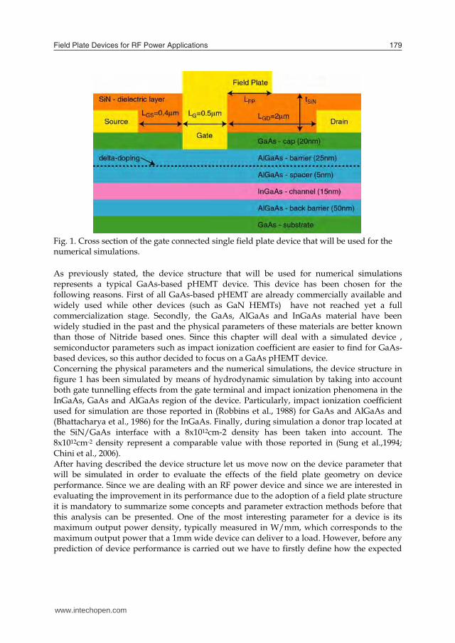
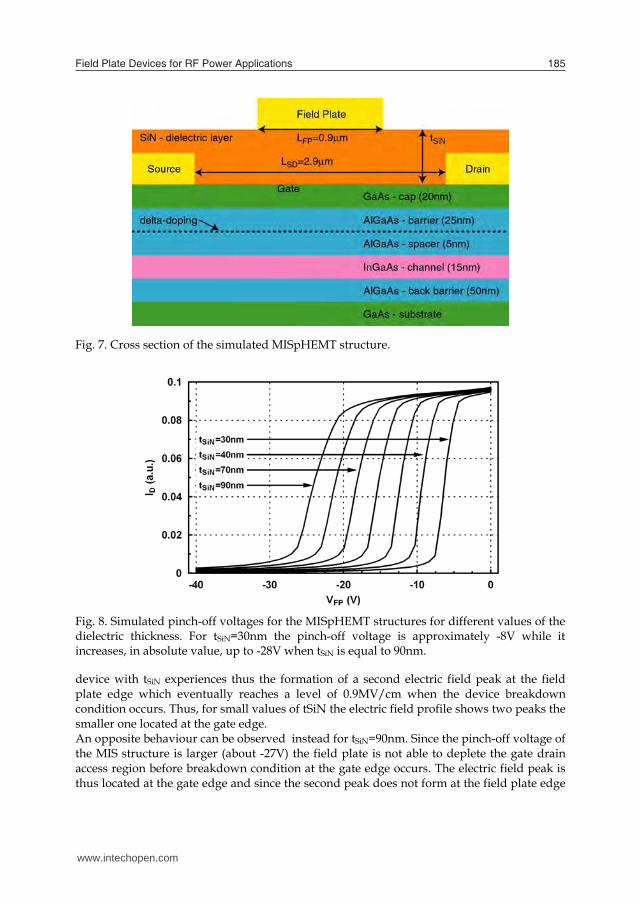
For the evaluation of the field plate benefits this author has decided to focus on a typical GaAs-based pHEMT device structure for power applications. All the numerical simulations that will be presented have been carried out by means of the commercial DESSIS-ISE (Synopsis Inc.) simulator. The device structure used for numerical simulations in this work is depicted in figure 1 and is composed as follows, starting from the bottom: a semi-insulating GaAs substrate, an undoped 50nm thick AlGaAs back-barrier, an undoped 15nm thick InGaAs channel, a 5nm thick AlGaAs spacer which is n-doped with a 2x10¹⁷(cm-3) concentration, a delta-doped layer with a concentration of 2x10¹²(cm-2), a 25nm thick AlGaAs barrier which is n-doped with a 2x10¹⁷(cm-3) concentration, a 20nm thick GaAs cap layer which is 2x10¹⁷(cm-3) n-doped. Although not necessary for the simulation process a brief description of a possible process for the realization of the simulated device is also provided in the following. The fabrication of pHEMT devices typically starts with the deposition of the source and drain ohmic contacts on the cap-layer followed by device isolation carried out either by ion-implantation or mesa isolation. A this point a SiN passivation layer is deposited, and its thickness (tSIN) will be one of the parameter that will be varied in order to evaluate field plate operation. After that SiN layer has been deposited a window is defined trough the SiN layer and the GaAs cap-layer is wet etched. In our case the defined window is 0.5m long which corresponds to the gate length of the simulated device. At this point, after a realignment lithographic step, the gate metal is evaporated forming both the gate contact and a field-plate which is formed by covering with the gate metal a portion of the SiN layer from the gate-edge toward the drain contact. The extension of the field plate (LFP) is the second parameter that will be analyzed in order to evaluate the effects of adding a gate connected single field plate structure. There are however others methods that can be used in order to fabricate field plated devices, although the resulting device behaves similarly to the one chosen here for carrying out numerical simulations. As proposed by (Chini et al., 2004) the field plate terminal can be formed on a passivated device by evaporating a second gate on top of the passivation layer and by forming an electrical connection between the gate and field plate terminal by using the common path of gate-pad and gate-feeder in the extrinsic device region.
As previously stated, the device structure that will be used for numerical simulations represents a typical GaAs-based pHEMT device. This device has been chosen for the following reasons. First of all GaAs-based pHEMT are already commercially available and widely used while other devices (such as GaN HEMTs) have not reached yet a full commercialization stage. Secondly, the GaAs, AlGaAs and InGaAs material have been widely studied in the past and the physical parameters of these materials are better known than those of Nitride based ones. Since this chapter will deal with a simulated device , semiconductor parameters such as impact ionization coefficient are easier to find for GaAs-based devices, so this author decided to focus on a GaAs pHEMT device. Concerning the physical parameters and the numerical simulations, the device structure in figure 1 has been simulated by means of hydrodynamic simulation by taking into account both gate tunnelling effects from the gate terminal and impact ionization phenomena in the InGaAs, GaAs and AlGaAs region of the device. Particularly, impact ionization coefficient used for simulation are those reported in (Robbins et al., 1988) for GaAs and AlGaAs and (Bhattacharya et al., 1986) for the InGaAs. Finally, during simulation a donor trap located at the SiN/GaAs interface with a 8x1012cm-2 density has been taken into account. The 8x1012cm-2 density represent a comparable value with those reported in (Sung et al.,1994; Chini et al., 2006). After having described the device structure let us move now on the device parameter that will be simulated in order to evaluate the effects of the field plate geometry on device performance. Since we are dealing with an RF power device and since we are interested in evaluating the improvement in its performance due to the adoption of a field plate structure it is mandatory to summarize some concepts and parameter extraction methods before that this analysis can be presented. One of the most interesting parameter for a device is its maximum output power density, typically measured in W/mm, which corresponds to the maximum output power that a 1mm wide device can deliver to a load. However, before any prediction of device performance is carried out we have to firstly define how the expected
Fig. 1. Cross section of the gate connected single field plate device that will be used for the numerical simulations.
www.intechopen.com
Field Plate Devices for RF Power Applications 179
pointing out that beside increasing the device operating voltage the field plate structure helps also in preventing drain current-collapse resulting in improved large signal RF performance compared to device without field plate. The aim of this chapter is to provide to the reader insights into field plate operation and its geometrical optimization. After giving some basic definitions concerning the operation of an RF-power device, which will be used in order to quantify the performance of the devices studied, the optimization of a gate-connected single field-plate GaAs-based pHEMT will be presented. Field plate geometrical parameters will be varied in order to show how they can affect device properties such as breakdown voltage, maximum output power and small signal performances. It will be thus possible to quantify the maximum improvement that can be achieved by using a gate connected single field plate. Finally, some advanced field plate structure will be discussed and compared in order to point out their advantages with respect to the gate connected single field plate structure.
2. Simulated device structure and simulation parameters
For the evaluation of the field plate benefits this author has decided to focus on a typical GaAs-based pHEMT device structure for power applications. All the numerical simulations that will be presented have been carried out by means of the commercial DESSIS-ISE (Synopsis Inc.) simulator. The device structure used for numerical simulations in this work is depicted in figure 1 and is composed as follows, starting from the bottom: a semi-insulating GaAs substrate, an undoped 50nm thick AlGaAs back-barrier, an undoped 15nm thick InGaAs channel, a 5nm thick AlGaAs spacer which is n-doped with a 2x10¹⁷(cm-3) concentration, a delta-doped layer with a concentration of 2x10¹²(cm-2), a 25nm thick AlGaAs barrier which is n-doped with a 2x10¹⁷(cm-3) concentration, a 20nm thick GaAs cap layer which is 2x10¹⁷(cm-3) n-doped. Although not necessary for the simulation process a brief description of a possible process for the realization of the simulated device is also provided in the following. The fabrication of pHEMT devices typically starts with the deposition of the source and drain ohmic contacts on the cap-layer followed by device isolation carried out either by ion-implantation or mesa isolation. A this point a SiN passivation layer is deposited, and its thickness (tSIN) will be one of the parameter that will be varied in order to evaluate field plate operation. After that SiN layer has been deposited a window is defined trough the SiN layer and the GaAs cap-layer is wet etched. In our case the defined window is 0.5m long which corresponds to the gate length of the simulated device. At this point, after a realignment lithographic step, the gate metal is evaporated forming both the gate contact and a field-plate which is formed by covering with the gate metal a portion of the SiN layer from the gate-edge toward the drain contact. The extension of the field plate (LFP) is the second parameter that will be analyzed in order to evaluate the effects of adding a gate connected single field plate structure. There are however others methods that can be used in order to fabricate field plated devices, although the resulting device behaves similarly to the one chosen here for carrying out numerical simulations. As proposed by (Chini et al., 2004) the field plate terminal can be formed on a passivated device by evaporating a second gate on top of the passivation layer and by forming an electrical connection between the gate and field plate terminal by using the common path of gate-pad and gate-feeder in the extrinsic device region.
As previously stated, the device structure that will be used for numerical simulations represents a typical GaAs-based pHEMT device. This device has been chosen for the following reasons. First of all GaAs-based pHEMT are already commercially available and widely used while other devices (such as GaN HEMTs) have not reached yet a full commercialization stage. Secondly, the GaAs, AlGaAs and InGaAs material have been widely studied in the past and the physical parameters of these materials are better known than those of Nitride based ones. Since this chapter will deal with a simulated device , semiconductor parameters such as impact ionization coefficient are easier to find for GaAs-based devices, so this author decided to focus on a GaAs pHEMT device. Concerning the physical parameters and the numerical simulations, the device structure in figure 1 has been simulated by means of hydrodynamic simulation by taking into account both gate tunnelling effects from the gate terminal and impact ionization phenomena in the InGaAs, GaAs and AlGaAs region of the device. Particularly, impact ionization coefficient used for simulation are those reported in (Robbins et al., 1988) for GaAs and AlGaAs and (Bhattacharya et al., 1986) for the InGaAs. Finally, during simulation a donor trap located at the SiN/GaAs interface with a 8x1012cm-2 density has been taken into account. The 8x1012cm-2 density represent a comparable value with those reported in (Sung et al.,1994; Chini et al., 2006). After having described the device structure let us move now on the device parameter that will be simulated in order to evaluate the effects of the field plate geometry on device performance. Since we are dealing with an RF power device and since we are interested in evaluating the improvement in its performance due to the adoption of a field plate structure it is mandatory to summarize some concepts and parameter extraction methods before that this analysis can be presented. One of the most interesting parameter for a device is its maximum output power density, typically measured in W/mm, which corresponds to the maximum output power that a 1mm wide device can deliver to a load. However, before any prediction of device performance is carried out we have to firstly define how the expected
Fig. 1. Cross section of the gate connected single field plate device that will be used for the numerical simulations.
www.intechopen.com
Advanced Microwave Circuits and Systems180
maximum output power can be extracted from the output I-V characteristics of said device. It can be shown (Cripps, 1999) that if the device drives a maximum current which is represented by IMAX, has a knee-voltage given by VKNEE and that the maximum applicable voltage is given by the breakdown voltage VBREAK the maximum linear power that can be obtained from the device when used as a class A linear amplifier is given by:
POUT,LIN=IMAX * (VBREAK-VKNEE) / 8 (1) If the maximum drain current IMAX is expressed in terms of A/mm equation 1 yields the maximum linear output power density. Another parameter that can be extracted, and usually easier to measure experimentally, is the saturated output power density. It can be demonstrated (Cripps, 1999) that the saturated output power is 2.1dB higher than the output linear power, or equivalently that:
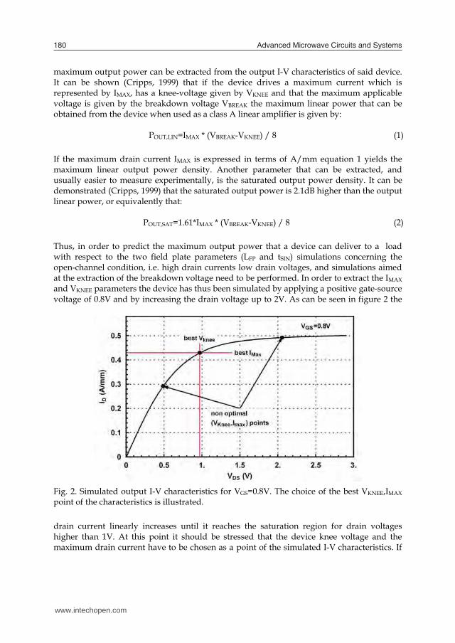
POUT,SAT=1.61*IMAX * (VBREAK-VKNEE) / 8 (2) Thus, in order to predict the maximum output power that a device can deliver to a load with respect to the two field plate parameters (LFP and tSIN) simulations concerning the open-channel condition, i.e. high drain currents low drain voltages, and simulations aimed at the extraction of the breakdown voltage need to be performed. In order to extract the IMAX and VKNEE parameters the device has thus been simulated by applying a positive gate-source voltage of 0.8V and by increasing the drain voltage up to 2V. As can be seen in figure 2 the
drain current linearly increases until it reaches the saturation region for drain voltages higher than 1V. At this point it should be stressed that the device knee voltage and the maximum drain current have to be chosen as a point of the simulated I-V characteristics. If
Fig. 2. Simulated output I-V characteristics for VGS=0.8V. The choice of the best VKNEE,IMAX
point of the characteristics is illustrated.
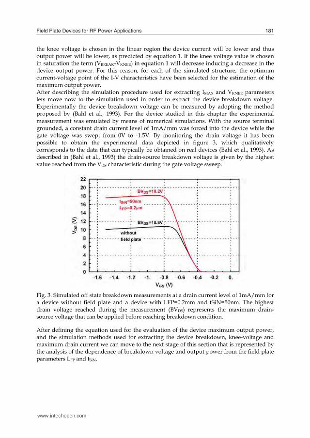
the knee voltage is chosen in the linear region the device current will be lower and thus output power will be lower, as predicted by equation 1. If the knee voltage value is chosen in saturation the term (VBREAK-VKNEE) in equation 1 will decrease inducing a decrease in the device output power. For this reason, for each of the simulated structure, the optimum current-voltage point of the I-V characteristics have been selected for the estimation of the maximum output power. After describing the simulation procedure used for extracting IMAX and VKNEE parameters lets move now to the simulation used in order to extract the device breakdown voltage. Experimentally the device breakdown voltage can be measured by adopting the method proposed by (Bahl et al., 1993). For the device studied in this chapter the experimental measurement was emulated by means of numerical simulations. With the source terminal grounded, a constant drain current level of 1mA/mm was forced into the device while the gate voltage was swept from 0V to -1.5V. By monitoring the drain voltage it has been possible to obtain the experimental data depicted in figure 3, which qualitatively corresponds to the data that can typically be obtained on real devices (Bahl et al., 1993). As described in (Bahl et al., 1993) the drain-source breakdown voltage is given by the highest value reached from the VDS characteristic during the gate voltage sweep.
After defining the equation used for the evaluation of the device maximum output power, and the simulation methods used for extracting the device breakdown, knee-voltage and maximum drain current we can move to the next stage of this section that is represented by the analysis of the dependence of breakdown voltage and output power from the field plate parameters LFP and tSiN.
Fig. 3. Simulated off state breakdown measurements at a drain current level of 1mA/mm fora device without field plate and a device with LFP=0.2mm and tSiN=50nm. The highestdrain voltage reached during the measurement (BVDS) represents the maximum drain-source voltage that can be applied before reaching breakdown condition.
www.intechopen.com
Field Plate Devices for RF Power Applications 181
maximum output power can be extracted from the output I-V characteristics of said device. It can be shown (Cripps, 1999) that if the device drives a maximum current which is represented by IMAX, has a knee-voltage given by VKNEE and that the maximum applicable voltage is given by the breakdown voltage VBREAK the maximum linear power that can be obtained from the device when used as a class A linear amplifier is given by:
POUT,LIN=IMAX * (VBREAK-VKNEE) / 8 (1) If the maximum drain current IMAX is expressed in terms of A/mm equation 1 yields the maximum linear output power density. Another parameter that can be extracted, and usually easier to measure experimentally, is the saturated output power density. It can be demonstrated (Cripps, 1999) that the saturated output power is 2.1dB higher than the output linear power, or equivalently that:
POUT,SAT=1.61*IMAX * (VBREAK-VKNEE) / 8 (2) Thus, in order to predict the maximum output power that a device can deliver to a load with respect to the two field plate parameters (LFP and tSIN) simulations concerning the open-channel condition, i.e. high drain currents low drain voltages, and simulations aimed at the extraction of the breakdown voltage need to be performed. In order to extract the IMAX and VKNEE parameters the device has thus been simulated by applying a positive gate-source voltage of 0.8V and by increasing the drain voltage up to 2V. As can be seen in figure 2 the
drain current linearly increases until it reaches the saturation region for drain voltages higher than 1V. At this point it should be stressed that the device knee voltage and the maximum drain current have to be chosen as a point of the simulated I-V characteristics. If
Fig. 2. Simulated output I-V characteristics for VGS=0.8V. The choice of the best VKNEE,IMAX
point of the characteristics is illustrated.
the knee voltage is chosen in the linear region the device current will be lower and thus output power will be lower, as predicted by equation 1. If the knee voltage value is chosen in saturation the term (VBREAK-VKNEE) in equation 1 will decrease inducing a decrease in the device output power. For this reason, for each of the simulated structure, the optimum current-voltage point of the I-V characteristics have been selected for the estimation of the maximum output power. After describing the simulation procedure used for extracting IMAX and VKNEE parameters lets move now to the simulation used in order to extract the device breakdown voltage. Experimentally the device breakdown voltage can be measured by adopting the method proposed by (Bahl et al., 1993). For the device studied in this chapter the experimental measurement was emulated by means of numerical simulations. With the source terminal grounded, a constant drain current level of 1mA/mm was forced into the device while the gate voltage was swept from 0V to -1.5V. By monitoring the drain voltage it has been possible to obtain the experimental data depicted in figure 3, which qualitatively corresponds to the data that can typically be obtained on real devices (Bahl et al., 1993). As described in (Bahl et al., 1993) the drain-source breakdown voltage is given by the highest value reached from the VDS characteristic during the gate voltage sweep.
After defining the equation used for the evaluation of the device maximum output power, and the simulation methods used for extracting the device breakdown, knee-voltage and maximum drain current we can move to the next stage of this section that is represented by the analysis of the dependence of breakdown voltage and output power from the field plate parameters LFP and tSiN.
Fig. 3. Simulated off state breakdown measurements at a drain current level of 1mA/mm fora device without field plate and a device with LFP=0.2mm and tSiN=50nm. The highestdrain voltage reached during the measurement (BVDS) represents the maximum drain-source voltage that can be applied before reaching breakdown condition.
www.intechopen.com
Advanced Microwave Circuits and Systems182
3. Breakdown dependence from field plate geometry
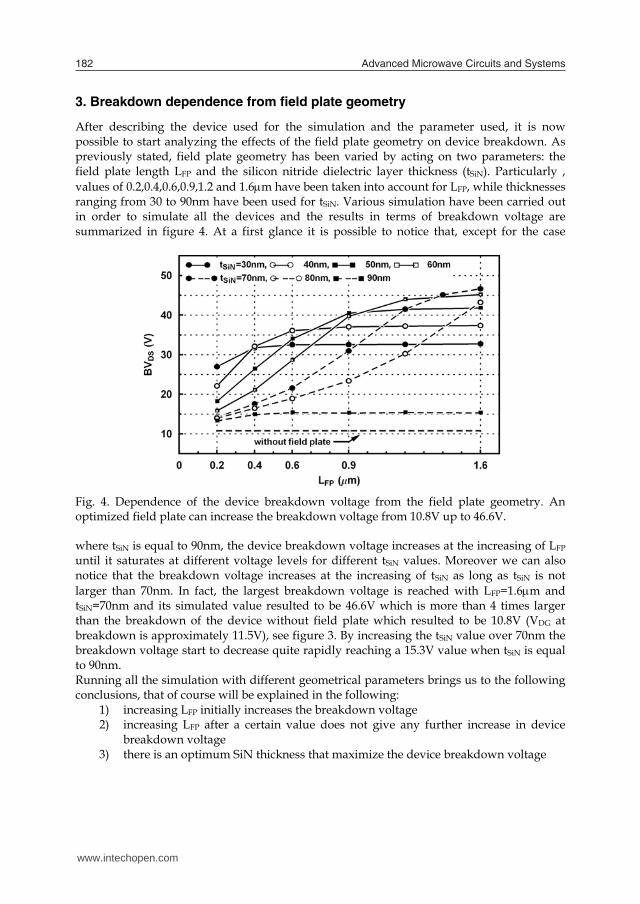
After describing the device used for the simulation and the parameter used, it is now possible to start analyzing the effects of the field plate geometry on device breakdown. As previously stated, field plate geometry has been varied by acting on two parameters: the field plate length LFP and the silicon nitride dielectric layer thickness (tSiN). Particularly , values of 0.2,0.4,0.6,0.9,1.2 and 1.6m have been taken into account for LFP, while thicknesses ranging from 30 to 90nm have been used for tSiN. Various simulation have been carried out in order to simulate all the devices and the results in terms of breakdown voltage are summarized in figure 4. At a first glance it is possible to notice that, except for the case
where tSiN is equal to 90nm, the device breakdown voltage increases at the increasing of LFP until it saturates at different voltage levels for different tSiN values. Moreover we can also notice that the breakdown voltage increases at the increasing of tSiN as long as tSiN is not larger than 70nm. In fact, the largest breakdown voltage is reached with LFP=1.6m and tSiN=70nm and its simulated value resulted to be 46.6V which is more than 4 times larger than the breakdown of the device without field plate which resulted to be 10.8V (VDG at breakdown is approximately 11.5V), see figure 3. By increasing the tSiN value over 70nm the breakdown voltage start to decrease quite rapidly reaching a 15.3V value when tSiN is equal to 90nm. Running all the simulation with different geometrical parameters brings us to the following conclusions, that of course will be explained in the following:
1) increasing LFP initially increases the breakdown voltage 2) increasing LFP after a certain value does not give any further increase in device
breakdown voltage 3) there is an optimum SiN thickness that maximize the device breakdown voltage
Fig. 4. Dependence of the device breakdown voltage from the field plate geometry. Anoptimized field plate can increase the breakdown voltage from 10.8V up to 46.6V.
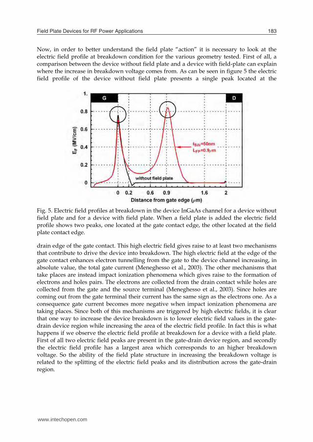
Now, in order to better understand the field plate “action” it is necessary to look at the electric field profile at breakdown condition for the various geometry tested. First of all, a comparison between the device without field plate and a device with field-plate can explain where the increase in breakdown voltage comes from. As can be seen in figure 5 the electric field profile of the device without field plate presents a single peak located at the
drain edge of the gate contact. This high electric field gives raise to at least two mechanisms that contribute to drive the device into breakdown. The high electric field at the edge of the gate contact enhances electron tunnelling from the gate to the device channel increasing, in absolute value, the total gate current (Meneghesso et al., 2003). The other mechanisms that take places are instead impact ionization phenomena which gives raise to the formation of electrons and holes pairs. The electrons are collected from the drain contact while holes are collected from the gate and the source terminal (Meneghesso et al., 2003). Since holes are coming out from the gate terminal their current has the same sign as the electrons one. As a consequence gate current becomes more negative when impact ionization phenomena are taking places. Since both of this mechanisms are triggered by high electric fields, it is clear that one way to increase the device breakdown is to lower electric field values in the gate-drain device region while increasing the area of the electric field profile. In fact this is what happens if we observe the electric field profile at breakdown for a device with a field plate. First of all two electric field peaks are present in the gate-drain device region, and secondly the electric field profile has a largest area which corresponds to an higher breakdown voltage. So the ability of the field plate structure in increasing the breakdown voltage is related to the splitting of the electric field peaks and its distribution across the gate-drain region.
Fig. 5. Electric field profiles at breakdown in the device InGaAs channel for a device withoutfield plate and for a device with field plate. When a field plate is added the electric fieldprofile shows two peaks, one located at the gate contact edge, the other located at the fieldplate contact edge.
www.intechopen.com
Field Plate Devices for RF Power Applications 183
3. Breakdown dependence from field plate geometry
After describing the device used for the simulation and the parameter used, it is now possible to start analyzing the effects of the field plate geometry on device breakdown. As previously stated, field plate geometry has been varied by acting on two parameters: the field plate length LFP and the silicon nitride dielectric layer thickness (tSiN). Particularly , values of 0.2,0.4,0.6,0.9,1.2 and 1.6m have been taken into account for LFP, while thicknesses ranging from 30 to 90nm have been used for tSiN. Various simulation have been carried out in order to simulate all the devices and the results in terms of breakdown voltage are summarized in figure 4. At a first glance it is possible to notice that, except for the case
where tSiN is equal to 90nm, the device breakdown voltage increases at the increasing of LFP until it saturates at different voltage levels for different tSiN values. Moreover we can also notice that the breakdown voltage increases at the increasing of tSiN as long as tSiN is not larger than 70nm. In fact, the largest breakdown voltage is reached with LFP=1.6m and tSiN=70nm and its simulated value resulted to be 46.6V which is more than 4 times larger than the breakdown of the device without field plate which resulted to be 10.8V (VDG at breakdown is approximately 11.5V), see figure 3. By increasing the tSiN value over 70nm the breakdown voltage start to decrease quite rapidly reaching a 15.3V value when tSiN is equal to 90nm. Running all the simulation with different geometrical parameters brings us to the following conclusions, that of course will be explained in the following:
1) increasing LFP initially increases the breakdown voltage 2) increasing LFP after a certain value does not give any further increase in device
breakdown voltage 3) there is an optimum SiN thickness that maximize the device breakdown voltage
Fig. 4. Dependence of the device breakdown voltage from the field plate geometry. Anoptimized field plate can increase the breakdown voltage from 10.8V up to 46.6V.
Now, in order to better understand the field plate “action” it is necessary to look at the electric field profile at breakdown condition for the various geometry tested. First of all, a comparison between the device without field plate and a device with field-plate can explain where the increase in breakdown voltage comes from. As can be seen in figure 5 the electric field profile of the device without field plate presents a single peak located at the
drain edge of the gate contact. This high electric field gives raise to at least two mechanisms that contribute to drive the device into breakdown. The high electric field at the edge of the gate contact enhances electron tunnelling from the gate to the device channel increasing, in absolute value, the total gate current (Meneghesso et al., 2003). The other mechanisms that take places are instead impact ionization phenomena which gives raise to the formation of electrons and holes pairs. The electrons are collected from the drain contact while holes are collected from the gate and the source terminal (Meneghesso et al., 2003). Since holes are coming out from the gate terminal their current has the same sign as the electrons one. As a consequence gate current becomes more negative when impact ionization phenomena are taking places. Since both of this mechanisms are triggered by high electric fields, it is clear that one way to increase the device breakdown is to lower electric field values in the gate-drain device region while increasing the area of the electric field profile. In fact this is what happens if we observe the electric field profile at breakdown for a device with a field plate. First of all two electric field peaks are present in the gate-drain device region, and secondly the electric field profile has a largest area which corresponds to an higher breakdown voltage. So the ability of the field plate structure in increasing the breakdown voltage is related to the splitting of the electric field peaks and its distribution across the gate-drain region.
Fig. 5. Electric field profiles at breakdown in the device InGaAs channel for a device withoutfield plate and for a device with field plate. When a field plate is added the electric fieldprofile shows two peaks, one located at the gate contact edge, the other located at the fieldplate contact edge.
www.intechopen.com
Advanced Microwave Circuits and Systems184
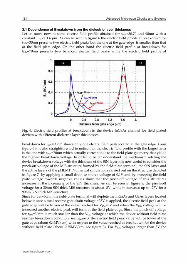
3.1 Dependence of Breakdown from the dielectric layer thickness Let us move now to some electric field profile obtained for tSiN=30,70 and 90nm with a constant LFP of 1.6 µm. As can be seen in figure 6 the electric field profile at breakdown for tSiN=30nm presents two electric field peaks but the one at the gate edge is smaller than that at the field plate edge. On the other hand the electric field profile at breakdown for tSiN=70nm presents two balanced electric field peaks while the electric field profile at
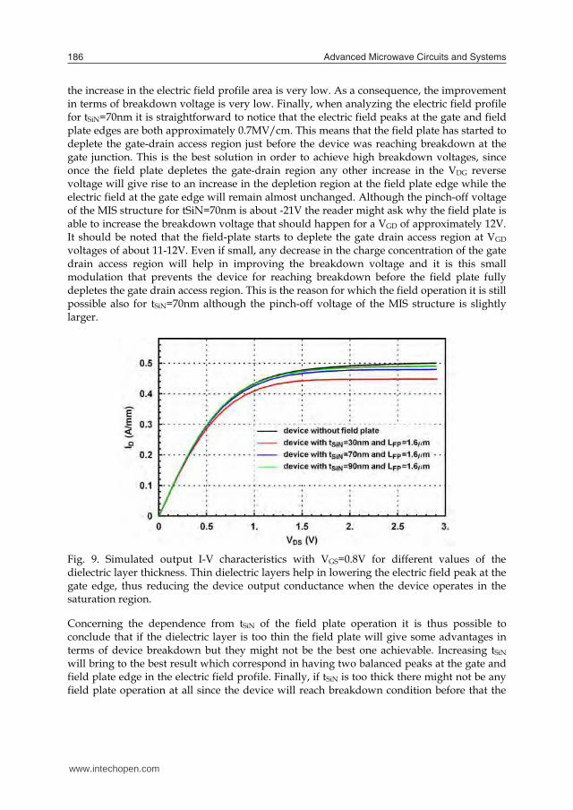
breakdown for tSiN=90nm shows only one electric field peak located at the gate edge. From figure 6 it is also straightforward to notice that the electric field profile with the largest area is the one with tSiN=70nm which actually corresponds to the field plate geometry that yields the highest breakdown voltage. In order to better understand the mechanism relating the device breakdown voltage with the thickness of the SiN layer it is now useful to consider the pinch-off voltage of the MIS structure formed by the field plate terminal, the SiN layer and the active layers of the pHEMT. Numerical simulations carried out on the structure depicted in figure 7 by applying a small drain to source voltage of 0.1V and by sweeping the field plate voltage towards negative values show that the pinch-off voltage of this structures increases at the increasing of the SiN thickness. As can be seen in figure 8, the pinch-off voltage for a 30nm SiN thick MIS structure is about -8V, while it increases up to -27V for a 90nm SiN thick MIS structure. Since for tSiN=30nm the field-plate terminal will deplete the InGaAs and GaAs layers located below it once a total reverse gate-drain voltage of 8V is applied, the electric field peak at the gate edge will be frozen at the value reached for VDG=8V and when the VDG voltage will be increased another electric peak will form at the field plate edge. Since the pinch-off voltage for tSiN=30nm is much smaller than the VGD voltage at which the device without field plate reaches breakdown condition, see figure 3, the electric field peak value will be lower at the gate edge (about 0.4MV/cm) with respect to the value reached at breakdown for the device without field plate (about 0.75MV/cm, see figure 3). For VDG voltages larger than 8V the
Fig. 6. Electric field profiles at breakdown in the device InGaAs channel for field plateddevices with different dielectric layer thicknesses.
device with tSiN experiences thus the formation of a second electric field peak at the field plate edge which eventually reaches a level of 0.9MV/cm when the device breakdown condition occurs. Thus, for small values of tSiN the electric field profile shows two peaks the smaller one located at the gate edge. An opposite behaviour can be observed instead for tSiN=90nm. Since the pinch-off voltage of the MIS structure is larger (about -27V) the field plate is not able to deplete the gate drain access region before breakdown condition at the gate edge occurs. The electric field peak is thus located at the gate edge and since the second peak does not form at the field plate edge
Fig. 8. Simulated pinch-off voltages for the MISpHEMT structures for different values of thedielectric thickness. For tSiN=30nm the pinch-off voltage is approximately -8V while itincreases, in absolute value, up to -28V when tSiN is equal to 90nm.
Fig. 7. Cross section of the simulated MISpHEMT structure.
www.intechopen.com
Field Plate Devices for RF Power Applications 185
3.1 Dependence of Breakdown from the dielectric layer thickness Let us move now to some electric field profile obtained for tSiN=30,70 and 90nm with a constant LFP of 1.6 µm. As can be seen in figure 6 the electric field profile at breakdown for tSiN=30nm presents two electric field peaks but the one at the gate edge is smaller than that at the field plate edge. On the other hand the electric field profile at breakdown for tSiN=70nm presents two balanced electric field peaks while the electric field profile at
breakdown for tSiN=90nm shows only one electric field peak located at the gate edge. From figure 6 it is also straightforward to notice that the electric field profile with the largest area is the one with tSiN=70nm which actually corresponds to the field plate geometry that yields the highest breakdown voltage. In order to better understand the mechanism relating the device breakdown voltage with the thickness of the SiN layer it is now useful to consider the pinch-off voltage of the MIS structure formed by the field plate terminal, the SiN layer and the active layers of the pHEMT. Numerical simulations carried out on the structure depicted in figure 7 by applying a small drain to source voltage of 0.1V and by sweeping the field plate voltage towards negative values show that the pinch-off voltage of this structures increases at the increasing of the SiN thickness. As can be seen in figure 8, the pinch-off voltage for a 30nm SiN thick MIS structure is about -8V, while it increases up to -27V for a 90nm SiN thick MIS structure. Since for tSiN=30nm the field-plate terminal will deplete the InGaAs and GaAs layers located below it once a total reverse gate-drain voltage of 8V is applied, the electric field peak at the gate edge will be frozen at the value reached for VDG=8V and when the VDG voltage will be increased another electric peak will form at the field plate edge. Since the pinch-off voltage for tSiN=30nm is much smaller than the VGD voltage at which the device without field plate reaches breakdown condition, see figure 3, the electric field peak value will be lower at the gate edge (about 0.4MV/cm) with respect to the value reached at breakdown for the device without field plate (about 0.75MV/cm, see figure 3). For VDG voltages larger than 8V the
Fig. 6. Electric field profiles at breakdown in the device InGaAs channel for field plateddevices with different dielectric layer thicknesses.
device with tSiN experiences thus the formation of a second electric field peak at the field plate edge which eventually reaches a level of 0.9MV/cm when the device breakdown condition occurs. Thus, for small values of tSiN the electric field profile shows two peaks the smaller one located at the gate edge. An opposite behaviour can be observed instead for tSiN=90nm. Since the pinch-off voltage of the MIS structure is larger (about -27V) the field plate is not able to deplete the gate drain access region before breakdown condition at the gate edge occurs. The electric field peak is thus located at the gate edge and since the second peak does not form at the field plate edge
Fig. 8. Simulated pinch-off voltages for the MISpHEMT structures for different values of thedielectric thickness. For tSiN=30nm the pinch-off voltage is approximately -8V while itincreases, in absolute value, up to -28V when tSiN is equal to 90nm.
Fig. 7. Cross section of the simulated MISpHEMT structure.
www.intechopen.com
Advanced Microwave Circuits and Systems186
the increase in the electric field profile area is very low. As a consequence, the improvement in terms of breakdown voltage is very low. Finally, when analyzing the electric field profile for tSiN=70nm it is straightforward to notice that the electric field peaks at the gate and field plate edges are both approximately 0.7MV/cm. This means that the field plate has started to deplete the gate-drain access region just before the device was reaching breakdown at the gate junction. This is the best solution in order to achieve high breakdown voltages, since once the field plate depletes the gate-drain region any other increase in the VDG reverse voltage will give rise to an increase in the depletion region at the field plate edge while the electric field at the gate edge will remain almost unchanged. Although the pinch-off voltage of the MIS structure for tSiN=70nm is about -21V the reader might ask why the field plate is able to increase the breakdown voltage that should happen for a VGD of approximately 12V. It should be noted that the field-plate starts to deplete the gate drain access region at VGD voltages of about 11-12V. Even if small, any decrease in the charge concentration of the gate drain access region will help in improving the breakdown voltage and it is this small modulation that prevents the device for reaching breakdown before the field plate fully depletes the gate drain access region. This is the reason for which the field operation it is still possible also for tSiN=70nm although the pinch-off voltage of the MIS structure is slightly larger.
Concerning the dependence from tSiN of the field plate operation it is thus possible to conclude that if the dielectric layer is too thin the field plate will give some advantages in terms of device breakdown but they might not be the best one achievable. Increasing tSiN will bring to the best result which correspond in having two balanced peaks at the gate and field plate edge in the electric field profile. Finally, if tSiN is too thick there might not be any field plate operation at all since the device will reach breakdown condition before that the
Fig. 9. Simulated output I-V characteristics with VGS=0.8V for different values of thedielectric layer thickness. Thin dielectric layers help in lowering the electric field peak at thegate edge, thus reducing the device output conductance when the device operates in thesaturation region.
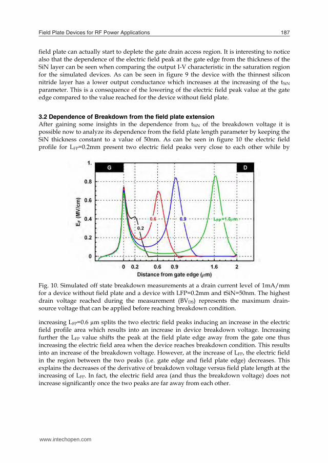
field plate can actually start to deplete the gate drain access region. It is interesting to notice also that the dependence of the electric field peak at the gate edge from the thickness of the SiN layer can be seen when comparing the output I-V characteristic in the saturation region for the simulated devices. As can be seen in figure 9 the device with the thinnest silicon nitride layer has a lower output conductance which increases at the increasing of the tSiN parameter. This is a consequence of the lowering of the electric field peak value at the gate edge compared to the value reached for the device without field plate.
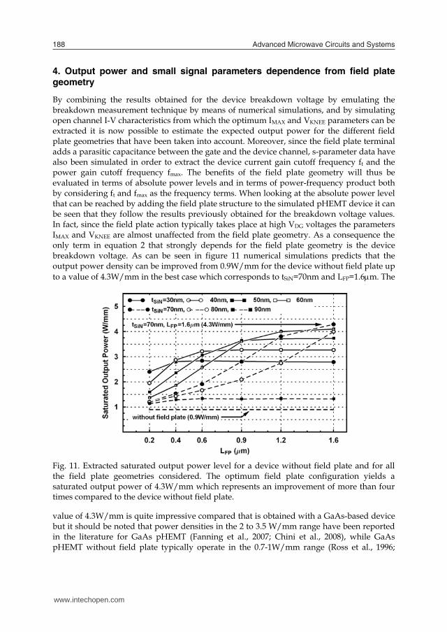
3.2 Dependence of Breakdown from the field plate extension After gaining some insights in the dependence from tSiN of the breakdown voltage it is possible now to analyze its dependence from the field plate length parameter by keeping the SiN thickness constant to a value of 50nm. As can be seen in figure 10 the electric field profile for LFP=0.2mm present two electric field peaks very close to each other while by
increasing LFP=0.6 µm splits the two electric field peaks inducing an increase in the electric field profile area which results into an increase in device breakdown voltage. Increasing further the LFP value shifts the peak at the field plate edge away from the gate one thus increasing the electric field area when the device reaches breakdown condition. This results into an increase of the breakdown voltage. However, at the increase of LFP, the electric field in the region between the two peaks (i.e. gate edge and field plate edge) decreases. This explains the decreases of the derivative of breakdown voltage versus field plate length at the increasing of LFP. In fact, the electric field area (and thus the breakdown voltage) does not increase significantly once the two peaks are far away from each other.
Fig. 10. Simulated off state breakdown measurements at a drain current level of 1mA/mmfor a device without field plate and a device with LFP=0.2mm and tSiN=50nm. The highestdrain voltage reached during the measurement (BVDS) represents the maximum drain-source voltage that can be applied before reaching breakdown condition.
www.intechopen.com
Field Plate Devices for RF Power Applications 187
the increase in the electric field profile area is very low. As a consequence, the improvement in terms of breakdown voltage is very low. Finally, when analyzing the electric field profile for tSiN=70nm it is straightforward to notice that the electric field peaks at the gate and field plate edges are both approximately 0.7MV/cm. This means that the field plate has started to deplete the gate-drain access region just before the device was reaching breakdown at the gate junction. This is the best solution in order to achieve high breakdown voltages, since once the field plate depletes the gate-drain region any other increase in the VDG reverse voltage will give rise to an increase in the depletion region at the field plate edge while the electric field at the gate edge will remain almost unchanged. Although the pinch-off voltage of the MIS structure for tSiN=70nm is about -21V the reader might ask why the field plate is able to increase the breakdown voltage that should happen for a VGD of approximately 12V. It should be noted that the field-plate starts to deplete the gate drain access region at VGD voltages of about 11-12V. Even if small, any decrease in the charge concentration of the gate drain access region will help in improving the breakdown voltage and it is this small modulation that prevents the device for reaching breakdown before the field plate fully depletes the gate drain access region. This is the reason for which the field operation it is still possible also for tSiN=70nm although the pinch-off voltage of the MIS structure is slightly larger.
Concerning the dependence from tSiN of the field plate operation it is thus possible to conclude that if the dielectric layer is too thin the field plate will give some advantages in terms of device breakdown but they might not be the best one achievable. Increasing tSiN will bring to the best result which correspond in having two balanced peaks at the gate and field plate edge in the electric field profile. Finally, if tSiN is too thick there might not be any field plate operation at all since the device will reach breakdown condition before that the
Fig. 9. Simulated output I-V characteristics with VGS=0.8V for different values of thedielectric layer thickness. Thin dielectric layers help in lowering the electric field peak at thegate edge, thus reducing the device output conductance when the device operates in thesaturation region.
field plate can actually start to deplete the gate drain access region. It is interesting to notice also that the dependence of the electric field peak at the gate edge from the thickness of the SiN layer can be seen when comparing the output I-V characteristic in the saturation region for the simulated devices. As can be seen in figure 9 the device with the thinnest silicon nitride layer has a lower output conductance which increases at the increasing of the tSiN parameter. This is a consequence of the lowering of the electric field peak value at the gate edge compared to the value reached for the device without field plate.
3.2 Dependence of Breakdown from the field plate extension After gaining some insights in the dependence from tSiN of the breakdown voltage it is possible now to analyze its dependence from the field plate length parameter by keeping the SiN thickness constant to a value of 50nm. As can be seen in figure 10 the electric field profile for LFP=0.2mm present two electric field peaks very close to each other while by
increasing LFP=0.6 µm splits the two electric field peaks inducing an increase in the electric field profile area which results into an increase in device breakdown voltage. Increasing further the LFP value shifts the peak at the field plate edge away from the gate one thus increasing the electric field area when the device reaches breakdown condition. This results into an increase of the breakdown voltage. However, at the increase of LFP, the electric field in the region between the two peaks (i.e. gate edge and field plate edge) decreases. This explains the decreases of the derivative of breakdown voltage versus field plate length at the increasing of LFP. In fact, the electric field area (and thus the breakdown voltage) does not increase significantly once the two peaks are far away from each other.
Fig. 10. Simulated off state breakdown measurements at a drain current level of 1mA/mmfor a device without field plate and a device with LFP=0.2mm and tSiN=50nm. The highestdrain voltage reached during the measurement (BVDS) represents the maximum drain-source voltage that can be applied before reaching breakdown condition.
www.intechopen.com
Advanced Microwave Circuits and Systems188
4. Output power and small signal parameters dependence from field plate geometry
By combining the results obtained for the device breakdown voltage by emulating the breakdown measurement technique by means of numerical simulations, and by simulating open channel I-V characteristics from which the optimum IMAX and VKNEE parameters can be extracted it is now possible to estimate the expected output power for the different field plate geometries that have been taken into account. Moreover, since the field plate terminal adds a parasitic capacitance between the gate and the device channel, s-parameter data have also been simulated in order to extract the device current gain cutoff frequency ft and the power gain cutoff frequency fmax. The benefits of the field plate geometry will thus be evaluated in terms of absolute power levels and in terms of power-frequency product both by considering ft and fmax as the frequency terms. When looking at the absolute power level that can be reached by adding the field plate structure to the simulated pHEMT device it can be seen that they follow the results previously obtained for the breakdown voltage values. In fact, since the field plate action typically takes place at high VDG voltages the parameters IMAX and VKNEE are almost unaffected from the field plate geometry. As a consequence the only term in equation 2 that strongly depends for the field plate geometry is the device breakdown voltage. As can be seen in figure 11 numerical simulations predicts that the output power density can be improved from 0.9W/mm for the device without field plate up to a value of 4.3W/mm in the best case which corresponds to tSiN=70nm and LFP=1.6m. The
value of 4.3W/mm is quite impressive compared that is obtained with a GaAs-based device but it should be noted that power densities in the 2 to 3.5 W/mm range have been reported in the literature for GaAs pHEMT (Fanning et al., 2007; Chini et al., 2008), while GaAs pHEMT without field plate typically operate in the 0.7-1W/mm range (Ross et al., 1996;
Fig. 11. Extracted saturated output power level for a device without field plate and for allthe field plate geometries considered. The optimum field plate configuration yields asaturated output power of 4.3W/mm which represents an improvement of more than fourtimes compared to the device without field plate.
Chini et al., 2008). The obtained 4.3W/mm value is of course optimistic since it does not take into account other phenomena, such as device self-heating, that might degrade device operation, nevertheless it gives us an important information in terms of which is the “boosting” factor of a gate connected single field plate structure. In terms of absolute power an optimized field plate device can reach power densities up to 4.7 times higher than the device without field plate. While everything seems to be very exciting in terms of output power it is now mandatory to evaluate the effects of the added field plate structure to the small-signal performances of the device. Several authors have reported a decrease in device power gain when adding field plate structures (Asano et al., 1998; Ando et al., 2003; Wu et al., 2004), and the main reason has been related to the added parasitic capacitance between the field plate and channel capacitance which gives rise to an increase in the device gate drain capacitance. The effect of increasing the gate drain capacitance is to reduce both the current gain cutoff frequency and the power gain cutoff frequency whose expression are given by (Ross et al., 1996):
ft=gm/[2л(CGS+CGD)] (3)
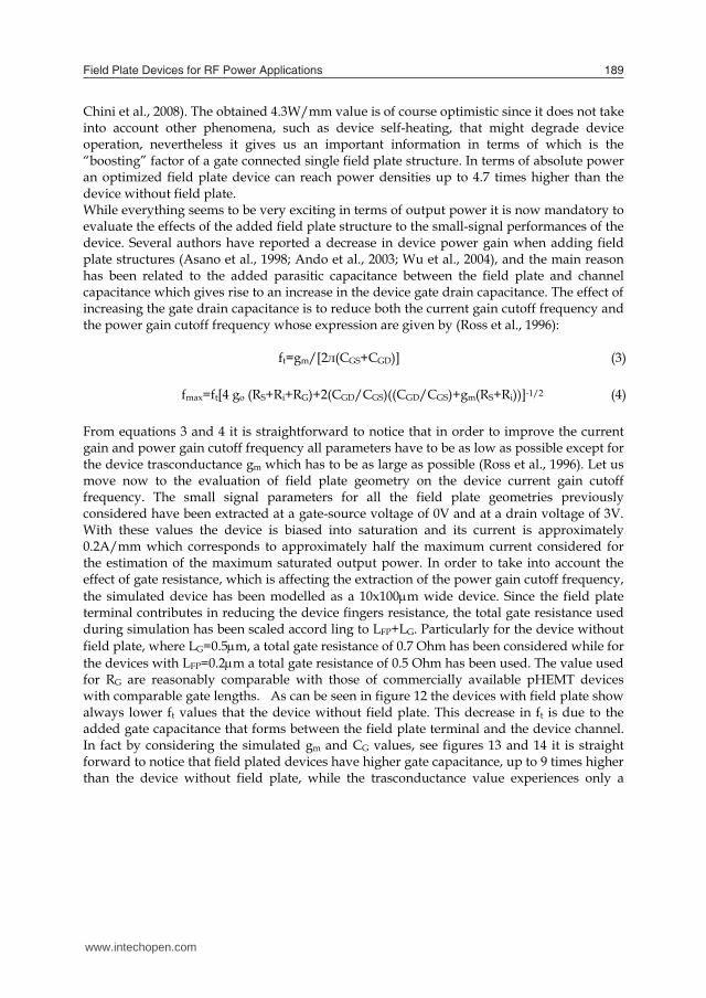
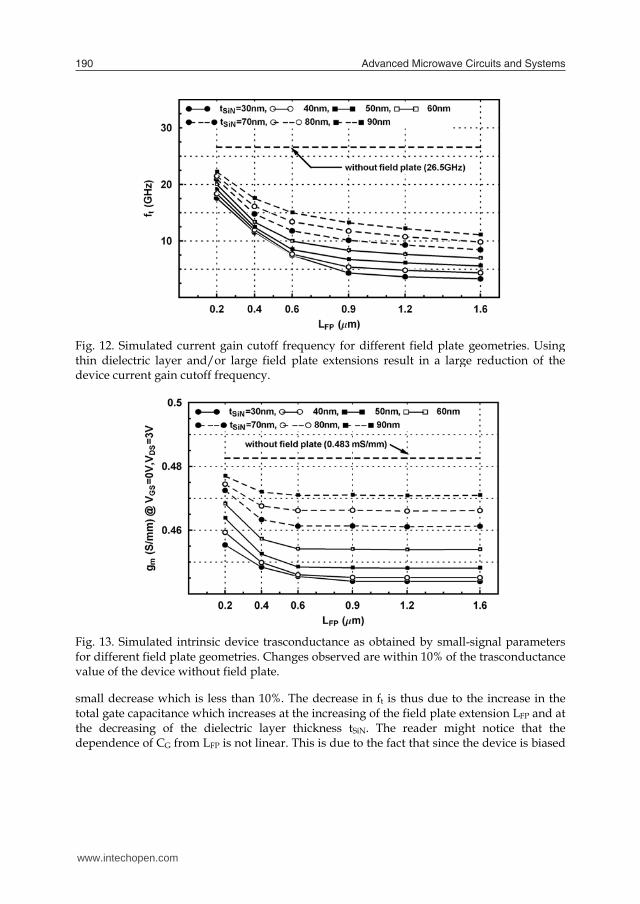
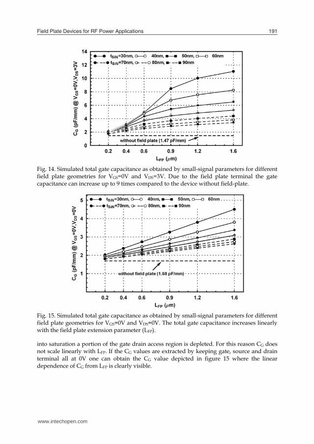
fmax=ft[4 go (RS+Ri+RG)+2(CGD/CGS)((CGD/CGS)+gm(RS+Ri))]-1/2 (4) From equations 3 and 4 it is straightforward to notice that in order to improve the current gain and power gain cutoff frequency all parameters have to be as low as possible except for the device trasconductance gm which has to be as large as possible (Ross et al., 1996). Let us move now to the evaluation of field plate geometry on the device current gain cutoff frequency. The small signal parameters for all the field plate geometries previously considered have been extracted at a gate-source voltage of 0V and at a drain voltage of 3V. With these values the device is biased into saturation and its current is approximately 0.2A/mm which corresponds to approximately half the maximum current considered for the estimation of the maximum saturated output power. In order to take into account the effect of gate resistance, which is affecting the extraction of the power gain cutoff frequency, the simulated device has been modelled as a 10x100m wide device. Since the field plate terminal contributes in reducing the device fingers resistance, the total gate resistance used during simulation has been scaled accord ling to LFP+LG. Particularly for the device without field plate, where LG=0.5m, a total gate resistance of 0.7 Ohm has been considered while for the devices with LFP=0.2m a total gate resistance of 0.5 Ohm has been used. The value used for RG are reasonably comparable with those of commercially available pHEMT devices with comparable gate lengths. As can be seen in figure 12 the devices with field plate show always lower ft values that the device without field plate. This decrease in ft is due to the added gate capacitance that forms between the field plate terminal and the device channel. In fact by considering the simulated gm and CG values, see figures 13 and 14 it is straight forward to notice that field plated devices have higher gate capacitance, up to 9 times higher than the device without field plate, while the trasconductance value experiences only a
www.intechopen.com
Field Plate Devices for RF Power Applications 189
4. Output power and small signal parameters dependence from field plate geometry
By combining the results obtained for the device breakdown voltage by emulating the breakdown measurement technique by means of numerical simulations, and by simulating open channel I-V characteristics from which the optimum IMAX and VKNEE parameters can be extracted it is now possible to estimate the expected output power for the different field plate geometries that have been taken into account. Moreover, since the field plate terminal adds a parasitic capacitance between the gate and the device channel, s-parameter data have also been simulated in order to extract the device current gain cutoff frequency ft and the power gain cutoff frequency fmax. The benefits of the field plate geometry will thus be evaluated in terms of absolute power levels and in terms of power-frequency product both by considering ft and fmax as the frequency terms. When looking at the absolute power level that can be reached by adding the field plate structure to the simulated pHEMT device it can be seen that they follow the results previously obtained for the breakdown voltage values. In fact, since the field plate action typically takes place at high VDG voltages the parameters IMAX and VKNEE are almost unaffected from the field plate geometry. As a consequence the only term in equation 2 that strongly depends for the field plate geometry is the device breakdown voltage. As can be seen in figure 11 numerical simulations predicts that the output power density can be improved from 0.9W/mm for the device without field plate up to a value of 4.3W/mm in the best case which corresponds to tSiN=70nm and LFP=1.6m. The
value of 4.3W/mm is quite impressive compared that is obtained with a GaAs-based device but it should be noted that power densities in the 2 to 3.5 W/mm range have been reported in the literature for GaAs pHEMT (Fanning et al., 2007; Chini et al., 2008), while GaAs pHEMT without field plate typically operate in the 0.7-1W/mm range (Ross et al., 1996;
Fig. 11. Extracted saturated output power level for a device without field plate and for allthe field plate geometries considered. The optimum field plate configuration yields asaturated output power of 4.3W/mm which represents an improvement of more than fourtimes compared to the device without field plate.
Chini et al., 2008). The obtained 4.3W/mm value is of course optimistic since it does not take into account other phenomena, such as device self-heating, that might degrade device operation, nevertheless it gives us an important information in terms of which is the “boosting” factor of a gate connected single field plate structure. In terms of absolute power an optimized field plate device can reach power densities up to 4.7 times higher than the device without field plate. While everything seems to be very exciting in terms of output power it is now mandatory to evaluate the effects of the added field plate structure to the small-signal performances of the device. Several authors have reported a decrease in device power gain when adding field plate structures (Asano et al., 1998; Ando et al., 2003; Wu et al., 2004), and the main reason has been related to the added parasitic capacitance between the field plate and channel capacitance which gives rise to an increase in the device gate drain capacitance. The effect of increasing the gate drain capacitance is to reduce both the current gain cutoff frequency and the power gain cutoff frequency whose expression are given by (Ross et al., 1996):
ft=gm/[2л(CGS+CGD)] (3)
fmax=ft[4 go (RS+Ri+RG)+2(CGD/CGS)((CGD/CGS)+gm(RS+Ri))]-1/2 (4) From equations 3 and 4 it is straightforward to notice that in order to improve the current gain and power gain cutoff frequency all parameters have to be as low as possible except for the device trasconductance gm which has to be as large as possible (Ross et al., 1996). Let us move now to the evaluation of field plate geometry on the device current gain cutoff frequency. The small signal parameters for all the field plate geometries previously considered have been extracted at a gate-source voltage of 0V and at a drain voltage of 3V. With these values the device is biased into saturation and its current is approximately 0.2A/mm which corresponds to approximately half the maximum current considered for the estimation of the maximum saturated output power. In order to take into account the effect of gate resistance, which is affecting the extraction of the power gain cutoff frequency, the simulated device has been modelled as a 10x100m wide device. Since the field plate terminal contributes in reducing the device fingers resistance, the total gate resistance used during simulation has been scaled accord ling to LFP+LG. Particularly for the device without field plate, where LG=0.5m, a total gate resistance of 0.7 Ohm has been considered while for the devices with LFP=0.2m a total gate resistance of 0.5 Ohm has been used. The value used for RG are reasonably comparable with those of commercially available pHEMT devices with comparable gate lengths. As can be seen in figure 12 the devices with field plate show always lower ft values that the device without field plate. This decrease in ft is due to the added gate capacitance that forms between the field plate terminal and the device channel. In fact by considering the simulated gm and CG values, see figures 13 and 14 it is straight forward to notice that field plated devices have higher gate capacitance, up to 9 times higher than the device without field plate, while the trasconductance value experiences only a
www.intechopen.com
Advanced Microwave Circuits and Systems190
small decrease which is less than 10%. The decrease in ft is thus due to the increase in the total gate capacitance which increases at the increasing of the field plate extension LFP and at the decreasing of the dielectric layer thickness tSiN. The reader might notice that the dependence of CG from LFP is not linear. This is due to the fact that since the device is biased
Fig. 13. Simulated intrinsic device trasconductance as obtained by small-signal parametersfor different field plate geometries. Changes observed are within 10% of the trasconductancevalue of the device without field plate.
Fig. 12. Simulated current gain cutoff frequency for different field plate geometries. Usingthin dielectric layer and/or large field plate extensions result in a large reduction of thedevice current gain cutoff frequency.
into saturation a portion of the gate drain access region is depleted. For this reason CG does not scale linearly with LFP. If the CG values are extracted by keeping gate, source and drain terminal all at 0V one can obtain the CG value depicted in figure 15 where the linear dependence of CG from LFP is clearly visible.
Fig. 15. Simulated total gate capacitance as obtained by small-signal parameters for differentfield plate geometries for VGS=0V and VDS=0V. The total gate capacitance increases linearlywith the field plate extension parameter (LFP).
Fig. 14. Simulated total gate capacitance as obtained by small-signal parameters for differentfield plate geometries for VGS=0V and VDS=3V. Due to the field plate terminal the gatecapacitance can increase up to 9 times compared to the device without field-plate.
www.intechopen.com
Field Plate Devices for RF Power Applications 191
small decrease which is less than 10%. The decrease in ft is thus due to the increase in the total gate capacitance which increases at the increasing of the field plate extension LFP and at the decreasing of the dielectric layer thickness tSiN. The reader might notice that the dependence of CG from LFP is not linear. This is due to the fact that since the device is biased
Fig. 13. Simulated intrinsic device trasconductance as obtained by small-signal parametersfor different field plate geometries. Changes observed are within 10% of the trasconductancevalue of the device without field plate.
Fig. 12. Simulated current gain cutoff frequency for different field plate geometries. Usingthin dielectric layer and/or large field plate extensions result in a large reduction of thedevice current gain cutoff frequency.
into saturation a portion of the gate drain access region is depleted. For this reason CG does not scale linearly with LFP. If the CG values are extracted by keeping gate, source and drain terminal all at 0V one can obtain the CG value depicted in figure 15 where the linear dependence of CG from LFP is clearly visible.
Fig. 15. Simulated total gate capacitance as obtained by small-signal parameters for differentfield plate geometries for VGS=0V and VDS=0V. The total gate capacitance increases linearlywith the field plate extension parameter (LFP).
Fig. 14. Simulated total gate capacitance as obtained by small-signal parameters for differentfield plate geometries for VGS=0V and VDS=3V. Due to the field plate terminal the gatecapacitance can increase up to 9 times compared to the device without field-plate.
www.intechopen.com
Advanced Microwave Circuits and Systems192
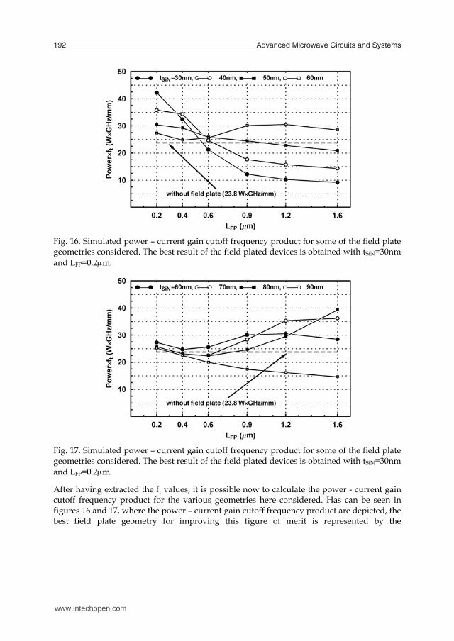
After having extracted the ft values, it is possible now to calculate the power - current gain cutoff frequency product for the various geometries here considered. Has can be seen in figures 16 and 17, where the power – current gain cutoff frequency product are depicted, the best field plate geometry for improving this figure of merit is represented by the
Fig. 17. Simulated power – current gain cutoff frequency product for some of the field plategeometries considered. The best result of the field plated devices is obtained with tSiN=30nmand LFP=0.2m.
Fig. 16. Simulated power – current gain cutoff frequency product for some of the field plategeometries considered. The best result of the field plated devices is obtained with tSiN=30nmand LFP=0.2m.
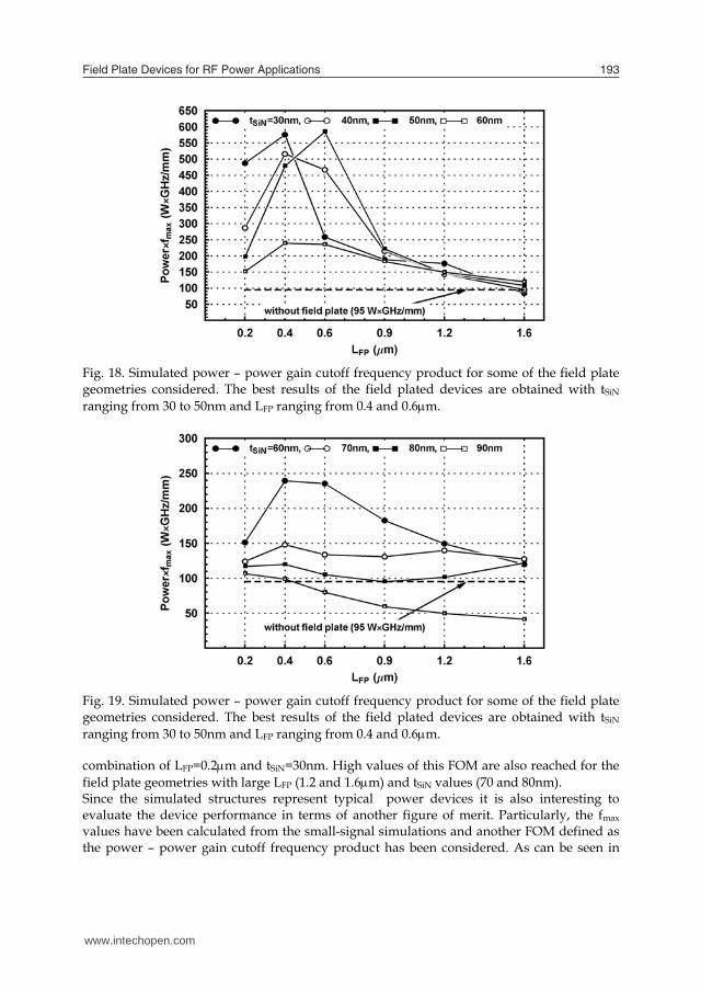
combination of LFP=0.2m and tSiN=30nm. High values of this FOM are also reached for the field plate geometries with large LFP (1.2 and 1.6m) and tSiN values (70 and 80nm). Since the simulated structures represent typical power devices it is also interesting to evaluate the device performance in terms of another figure of merit. Particularly, the fmax
values have been calculated from the small-signal simulations and another FOM defined as the power – power gain cutoff frequency product has been considered. As can be seen in
Fig. 19. Simulated power – power gain cutoff frequency product for some of the field plategeometries considered. The best results of the field plated devices are obtained with tSiN
ranging from 30 to 50nm and LFP ranging from 0.4 and 0.6m.
Fig. 18. Simulated power – power gain cutoff frequency product for some of the field plategeometries considered. The best results of the field plated devices are obtained with tSiN
ranging from 30 to 50nm and LFP ranging from 0.4 and 0.6m.
www.intechopen.com
Field Plate Devices for RF Power Applications 193
After having extracted the ft values, it is possible now to calculate the power - current gain cutoff frequency product for the various geometries here considered. Has can be seen in figures 16 and 17, where the power – current gain cutoff frequency product are depicted, the best field plate geometry for improving this figure of merit is represented by the
Fig. 17. Simulated power – current gain cutoff frequency product for some of the field plategeometries considered. The best result of the field plated devices is obtained with tSiN=30nmand LFP=0.2m.
Fig. 16. Simulated power – current gain cutoff frequency product for some of the field plategeometries considered. The best result of the field plated devices is obtained with tSiN=30nmand LFP=0.2m.
combination of LFP=0.2m and tSiN=30nm. High values of this FOM are also reached for the field plate geometries with large LFP (1.2 and 1.6m) and tSiN values (70 and 80nm). Since the simulated structures represent typical power devices it is also interesting to evaluate the device performance in terms of another figure of merit. Particularly, the fmax
values have been calculated from the small-signal simulations and another FOM defined as the power – power gain cutoff frequency product has been considered. As can be seen in
Fig. 19. Simulated power – power gain cutoff frequency product for some of the field plategeometries considered. The best results of the field plated devices are obtained with tSiN
ranging from 30 to 50nm and LFP ranging from 0.4 and 0.6m.
Fig. 18. Simulated power – power gain cutoff frequency product for some of the field plategeometries considered. The best results of the field plated devices are obtained with tSiN
ranging from 30 to 50nm and LFP ranging from 0.4 and 0.6m.
www.intechopen.com
Advanced Microwave Circuits and Systems194
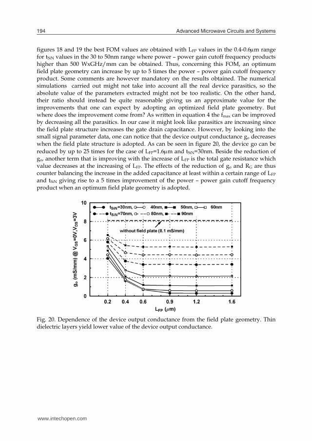
figures 18 and 19 the best FOM values are obtained with LFP values in the 0.4-0.6m range for tSiN values in the 30 to 50nm range where power – power gain cutoff frequency products higher than 500 WxGHz/mm can be obtained. Thus, concerning this FOM, an optimum field plate geometry can increase by up to 5 times the power – power gain cutoff frequency product. Some comments are however mandatory on the results obtained. The numerical simulations carried out might not take into account all the real device parasitics, so the absolute value of the parameters extracted might not be too realistic. On the other hand, their ratio should instead be quite reasonable giving us an approximate value for the improvements that one can expect by adopting an optimized field plate geometry. But where does the improvement come from? As written in equation 4 the fmax can be improved by decreasing all the parasitics. In our case it might look like parasitics are increasing since the field plate structure increases the gate drain capacitance. However, by looking into the small signal parameter data, one can notice that the device output conductance go decreases when the field plate structure is adopted. As can be seen in figure 20, the device go can be reduced by up to 25 times for the case of LFP=1.6m and tSiN=30nm. Beside the reduction of go, another term that is improving with the increase of LFP is the total gate resistance which value decreases at the increasing of LFP. The effects of the reduction of go and RG are thus counter balancing the increase in the added capacitance at least within a certain range of LFP and tSiN giving rise to a 5 times improvement of the power – power gain cutoff frequency product when an optimum field plate geometry is adopted.
Fig. 20. Dependence of the device output conductance from the field plate geometry. Thindielectric layers yield lower value of the device output conductance.
5. Advanced field plate structures
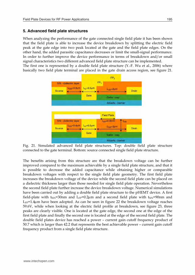
When analyzing the performance of the gate connected single field plate it has been shown that the field plate is able to increase the device breakdown by splitting the electric field peak at the gate edge into two peak located at the gate and the field plate edges. On the other hand, the added parasitic capacitance decreases or limit the small-signal performance. In order to further improve the device performance in terms of breakdown and/or small signal characteristics two different advanced field plate structure can be implemented. The first one is represented by a double field plate structure (Y.-F. Wu et al., 2006) where basically two field plate terminal are placed in the gate drain access region, see figure 21.
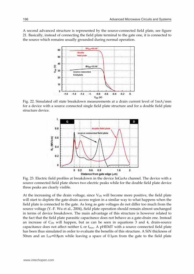
The benefits arising from this structure are that the breakdown voltage can be further improved compared to the maximum achievable by a single field plate structure, and that it is possible to decrease the added capacitance while obtaining higher or comparable breakdown voltages with respect to the single field plate geometry. The first field plate increases the breakdown voltage of the device while the second field plate can be placed on a dielectric thickness larger than those needed for single field plate operation. Nevertheless the second field plate further increase the device breakdown voltage. Numerical simulations have been carried out by adding a double field plate structure to the pHEMT device. A first field-plate with tSiN=30nm and LFP=0.2m and a second field plate with tSiN=90nm and LFP=1.4m have been adopted. As can be seen in figure 22 the breakdown voltage reaches 59.6V, while when looking at the electric field profile at breakdown, see figure 23, three peaks are clearly visible. One is located at the gate edge, the second one at the edge of the first field plate and finally the second one is located at the edge of the second field plate. The double field plates device has reached a power – current gain cutoff frequency product of 50.7 which is larger than 42.2 that represents the best achievable power – current gain cutoff frequency product from a single field plate structure.
Fig. 21. Simulated advanced field plate structures. Top: double field plate structureconnected to the gate terminal. Bottom: source connected single field plate structure.
www.intechopen.com
Field Plate Devices for RF Power Applications 195
figures 18 and 19 the best FOM values are obtained with LFP values in the 0.4-0.6m range for tSiN values in the 30 to 50nm range where power – power gain cutoff frequency products higher than 500 WxGHz/mm can be obtained. Thus, concerning this FOM, an optimum field plate geometry can increase by up to 5 times the power – power gain cutoff frequency product. Some comments are however mandatory on the results obtained. The numerical simulations carried out might not take into account all the real device parasitics, so the absolute value of the parameters extracted might not be too realistic. On the other hand, their ratio should instead be quite reasonable giving us an approximate value for the improvements that one can expect by adopting an optimized field plate geometry. But where does the improvement come from? As written in equation 4 the fmax can be improved by decreasing all the parasitics. In our case it might look like parasitics are increasing since the field plate structure increases the gate drain capacitance. However, by looking into the small signal parameter data, one can notice that the device output conductance go decreases when the field plate structure is adopted. As can be seen in figure 20, the device go can be reduced by up to 25 times for the case of LFP=1.6m and tSiN=30nm. Beside the reduction of go, another term that is improving with the increase of LFP is the total gate resistance which value decreases at the increasing of LFP. The effects of the reduction of go and RG are thus counter balancing the increase in the added capacitance at least within a certain range of LFP and tSiN giving rise to a 5 times improvement of the power – power gain cutoff frequency product when an optimum field plate geometry is adopted.
Fig. 20. Dependence of the device output conductance from the field plate geometry. Thindielectric layers yield lower value of the device output conductance.
5. Advanced field plate structures
When analyzing the performance of the gate connected single field plate it has been shown that the field plate is able to increase the device breakdown by splitting the electric field peak at the gate edge into two peak located at the gate and the field plate edges. On the other hand, the added parasitic capacitance decreases or limit the small-signal performance. In order to further improve the device performance in terms of breakdown and/or small signal characteristics two different advanced field plate structure can be implemented. The first one is represented by a double field plate structure (Y.-F. Wu et al., 2006) where basically two field plate terminal are placed in the gate drain access region, see figure 21.
The benefits arising from this structure are that the breakdown voltage can be further improved compared to the maximum achievable by a single field plate structure, and that it is possible to decrease the added capacitance while obtaining higher or comparable breakdown voltages with respect to the single field plate geometry. The first field plate increases the breakdown voltage of the device while the second field plate can be placed on a dielectric thickness larger than those needed for single field plate operation. Nevertheless the second field plate further increase the device breakdown voltage. Numerical simulations have been carried out by adding a double field plate structure to the pHEMT device. A first field-plate with tSiN=30nm and LFP=0.2m and a second field plate with tSiN=90nm and LFP=1.4m have been adopted. As can be seen in figure 22 the breakdown voltage reaches 59.6V, while when looking at the electric field profile at breakdown, see figure 23, three peaks are clearly visible. One is located at the gate edge, the second one at the edge of the first field plate and finally the second one is located at the edge of the second field plate. The double field plates device has reached a power – current gain cutoff frequency product of 50.7 which is larger than 42.2 that represents the best achievable power – current gain cutoff frequency product from a single field plate structure.
Fig. 21. Simulated advanced field plate structures. Top: double field plate structureconnected to the gate terminal. Bottom: source connected single field plate structure.
www.intechopen.com
Advanced Microwave Circuits and Systems196
A second advanced structure is represented by the source-connected field plate, see figure 21. Basically, instead of connecting the field plate terminal to the gate one, it is connected to the source which remains usually grounded during normal operation.
At the increasing of the drain voltage, since VDS will become more positive, the field plate will start to deplete the gate-drain access region in a similar way to what happens when the field plate is connected to the gate. As long as gate voltages do not differ too much from the source voltage (Y.-F. Wu et al., 2004), field plate operation should remain almost unchanged in terms of device breakdown. The main advantage of this structure is however related to the fact that the field plate parasitic capacitance does not behave as a gate-drain one. Instead an increase of CDS will happen, but as can be seen in equations 3 and 4, drain-source capacitance does not affect neither ft or fmax. A pHEMT with a source connected field plate has been thus simulated in order to evaluate the benefits of this structure. A SiN thickness of 50nm and an LFP=0.8m while leaving a space of 0.1m from the gate to the field plate
Fig. 23. Electric field profiles at breakdown in the device InGaAs channel. The device with asource connected field plate shows two electric peaks while for the double field plate devicethree peaks are clearly visible.
Fig. 22. Simulated off state breakdown measurements at a drain current level of 1mA/mmfor a device with a source connected single field plate structure and for a double field platestructure device.
contact was implemented, see figure 21. An off-state breakdown voltage of 33.4V was obtained, see figure 22, while the electric field profile at breakdown behaves in a similar way to those achievable with a gate connected field plate, see figure 23. The most interesting results are however related to the improvements in terms of small signal performance. The source connected field plate device has reached a power – current gain cutoff frequency product of 80.5 which is almost twice than 42.2 that represents the best achievable power – current gain cutoff frequency product from a single field plate structure.
6. Conclusions
Numerical simulations carried out on different field plate geometries applied to a GaAs-based pHEMT have yielded some insights on the improvements and the limitations of said structures. Field plate structure has been and will be used for the fabrication of power devices due to the extremely high benefits that can arise from this structure. It has been shown that although parasitic capacitance are added to the device, its performance can greatly improve both in terms of the power – current gain cutoff frequency and the power – power gain cutoff frequency products. The main parameter for some of the field plate geometries considered and for the two advanced structure discussed in the previous section are reported in table 1. Device# 1 2 3 4 5 6 tSiN (nm) 0 300 500 700 500 (Source) 300/900 LFP (mm) 0 0.2 0.6 1.6 0.9 0.2/1.4 BVDS (V) 10.8 27 34 46.6 33.4 59.4 Pout (W/mm) 0.9
2.4 3 4.3
3 5.5
ft (GHz) 26.6 17.6 8.5 8.4 27.2 9.3 FOM1 (W GHz/mm) 23.8 42.2 25.8 36.2 80.5 50.7 FOM2 (W GHz/mm) 95 480 585 130 920 180
Table 1. Breakdown voltage (BVDS), maximum output power (Pout), current gain cutoff frequency (ft), power-current gain cutoff frequency product (FOM1) and power-power gain cutoff frequency product (FOM2) for some of the field plate structures and geometries that have been simulated. From the value reported in table 1 it is clear that field plate parameters have of course to be tailored to the specific application in order to achieve the best results: higher operating voltages and/or output power densities can be obtained at the expenses of power gain. Advanced structures such as source connected field plate and double field plates can further improve devices performances by dramatically improving the small signal performance in the case of the source connected field plate or by further increasing the device operating voltages in the case of the double field plate structure.
7. References
Ando Y., Okamoto Y., Miyamoto H., Nakayama T., Inoue T., and Kuzuhara M. (2003) “10-W/mm AlGaN-GaN HFET With a Field Modulatine Plate”, IEEE Electron Device Letters, Vol. 24, No. 5, pp. 289-291, May 2003.
www.intechopen.com
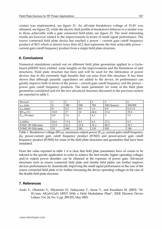
Field Plate Devices for RF Power Applications 197
A second advanced structure is represented by the source-connected field plate, see figure 21. Basically, instead of connecting the field plate terminal to the gate one, it is connected to the source which remains usually grounded during normal operation.
At the increasing of the drain voltage, since VDS will become more positive, the field plate will start to deplete the gate-drain access region in a similar way to what happens when the field plate is connected to the gate. As long as gate voltages do not differ too much from the source voltage (Y.-F. Wu et al., 2004), field plate operation should remain almost unchanged in terms of device breakdown. The main advantage of this structure is however related to the fact that the field plate parasitic capacitance does not behave as a gate-drain one. Instead an increase of CDS will happen, but as can be seen in equations 3 and 4, drain-source capacitance does not affect neither ft or fmax. A pHEMT with a source connected field plate has been thus simulated in order to evaluate the benefits of this structure. A SiN thickness of 50nm and an LFP=0.8m while leaving a space of 0.1m from the gate to the field plate
Fig. 23. Electric field profiles at breakdown in the device InGaAs channel. The device with asource connected field plate shows two electric peaks while for the double field plate devicethree peaks are clearly visible.
Fig. 22. Simulated off state breakdown measurements at a drain current level of 1mA/mmfor a device with a source connected single field plate structure and for a double field platestructure device.
contact was implemented, see figure 21. An off-state breakdown voltage of 33.4V was obtained, see figure 22, while the electric field profile at breakdown behaves in a similar way to those achievable with a gate connected field plate, see figure 23. The most interesting results are however related to the improvements in terms of small signal performance. The source connected field plate device has reached a power – current gain cutoff frequency product of 80.5 which is almost twice than 42.2 that represents the best achievable power – current gain cutoff frequency product from a single field plate structure.
6. Conclusions
Numerical simulations carried out on different field plate geometries applied to a GaAs-based pHEMT have yielded some insights on the improvements and the limitations of said structures. Field plate structure has been and will be used for the fabrication of power devices due to the extremely high benefits that can arise from this structure. It has been shown that although parasitic capacitance are added to the device, its performance can greatly improve both in terms of the power – current gain cutoff frequency and the power – power gain cutoff frequency products. The main parameter for some of the field plate geometries considered and for the two advanced structure discussed in the previous section are reported in table 1. Device# 1 2 3 4 5 6 tSiN (nm) 0 300 500 700 500 (Source) 300/900 LFP (mm) 0 0.2 0.6 1.6 0.9 0.2/1.4 BVDS (V) 10.8 27 34 46.6 33.4 59.4 Pout (W/mm) 0.9
2.4 3 4.3
3 5.5
ft (GHz) 26.6 17.6 8.5 8.4 27.2 9.3 FOM1 (W GHz/mm) 23.8 42.2 25.8 36.2 80.5 50.7 FOM2 (W GHz/mm) 95 480 585 130 920 180
Table 1. Breakdown voltage (BVDS), maximum output power (Pout), current gain cutoff frequency (ft), power-current gain cutoff frequency product (FOM1) and power-power gain cutoff frequency product (FOM2) for some of the field plate structures and geometries that have been simulated. From the value reported in table 1 it is clear that field plate parameters have of course to be tailored to the specific application in order to achieve the best results: higher operating voltages and/or output power densities can be obtained at the expenses of power gain. Advanced structures such as source connected field plate and double field plates can further improve devices performances by dramatically improving the small signal performance in the case of the source connected field plate or by further increasing the device operating voltages in the case of the double field plate structure.
7. References
Ando Y., Okamoto Y., Miyamoto H., Nakayama T., Inoue T., and Kuzuhara M. (2003) “10-W/mm AlGaN-GaN HFET With a Field Modulatine Plate”, IEEE Electron Device Letters, Vol. 24, No. 5, pp. 289-291, May 2003.
www.intechopen.com
Advanced Microwave Circuits and Systems198
Asano K., Miyoshi Y., Ishikura K., Nashimoto Y., Kuzuhara M., and Mizuta M. (1998) “Novel high power AlGaAs/GaAs HFET with a field-modulating plate operated at 35 V drain voltage”, Proceedins of the International Electron Devices Meeting (IEDM ’98), pp. 59-62, 6-9 Dec. 1998.
Bahl S. R., and del Alamo J. A. (1993), “A New Drain Injection Technique for the Measurement of Off-State Breakdown Voltage in FET’s”, IEEE Transactions on Electron Devices, Vol. 40, No. 8, pp. 1558-1560, Aug. 1993.
Bhattacharya P. K., Das U., Juang F. Y., Nashimoto Y., and S. Dhar, (1986), “Material properties and optical guiding in InGaAs-GaAs strained layer superlattices-a brief review”, Solid-State Electronics, Vol. 29, No. 2, pp. 261-267, February 1986.
Chini A., Buttari D., Coffie R., Heikman S., Keller S., and Mishra U. K., (2004), “12 W/mm power density AlGaN/GaN HEMTs on sapphire substrate”, IET Electronics Letters, Vol. 40, No. 1, pp. 73-74, Jan. 2004.
Chini A., S. Lavanga, M. Peroni, C. Lanzieri, A. Cetronio, V. Teppati, V. Camarchia, G. Ghione, and G. Verzellesi (2006) “Fabrication Characetrization and Numerical Simulation of High Breakdown Voltage pHEMTs”, Proceedings of the 1st European Microwave Integrated Circuits Conference, pp. 50-54, Sept. 2006.
Chini A., Esposto M., verzellesi G., Lavanga S., C. Lanzieri, A. Cetronio (2008) “Characterization and Numerical Simulations of High Power Field-Plated pHEMTs”, Proceedings of the 3rd European Microwave Integrated Circuits Conference, pp. 218-222, Oct. 2008.
Cripps S. C. (1999) “RF Power Amplifiers for Wireless Communications”, Artech House, ISBN 0-89006-989-1.
Fanning D., Balistreri A., Beam III E., Decker K., Evans S., Eye R., Gaiewski W., Nagle T., Saunier P., and Tserng H.-Q. (2007) “High Voltage GaAs pHEMT Technology for S-band High Power Amplifiers”, CS MANTECH Conference, Austin, Texas, pp. 173-176, 14-17 May 2007
Johnson E. O., (1965), “Physical limitation on frequency and power parameters of transistors “, RCA Rev., pp. 163–176, Jun. 1965.
Meneghesso G., Chini A., Maretto M., and Zanoni E. (2003), “Pulsed Measurements and Circuit Modeling of Weak and Strong Avalanche Effects in GaAs MESFETs and HEMTs”, IEEE Transactions on Electron Devices, Vol. 50, No. 2, pp. 324-332, Feb. 2003.
Robbins V. M., Smith S. C., and Stillman G. E. (1988), “Impact ionization in AlxGa1-xAs for x=0.1-0.4”, Applied Physics Letters, Vol. 52, No. 4, pp. 296-298, 1988.
Ross R. L., Svensson S. P., and Lugli P. (1996) “Pseudomorphic Hemt Technolgy and Applications”, Springer, ISBN 0792339150.
Sung Y.-K., Kim J.-K., Ju Y.-J., and Ryoo J.-H. (1994), “The Passivation of GaAs by laser CVD”, Proceedings of the 44th Electronic and Technolgy Conference, pp. 635-639, 1-4 May 1994.
Wu Y.-F., Saxler A., Moore M., Smith R.P., Sheppard S., Chavarkar P.M., Wisleder T., Mishra U.K., and Parikh P. (2004) “30-W/mm GaN HEMTs by field plate optimization”, IEEE Electron Device Letters, Vol. 25, No. 3, pp. 117-119, Mar. 2004.
Wu Y.-F., Moore M., Wisleder T., Chavarkar P.M., Mishra U.K. and Parikh P. (2004) “High-gain Microwave GaN HEMTs with Source-terminated Field-plates”, Proceedins of the International Electron Device Meeting (IEDM ’04), pp. 1078-1079, 13-15 Dec. 2004.
Wu Y.-F., Moore M., Wisleder T., and Parikh P. (2006) “40-W/mm Double Field-plated GaN HEMTs”, Proceedins of the 64th Device Research Conference, pp. 151-152, June 2006.
www.intechopen.com

Advanced Microwave Circuits and SystemsEdited by Vitaliy Zhurbenko
ISBN 978-953-307-087-2Hard cover, 490 pagesPublisher InTechPublished online 01, April, 2010Published in print edition April, 2010
InTech EuropeUniversity Campus STeP Ri Slavka Krautzeka 83/A 51000 Rijeka, Croatia Phone: +385 (51) 770 447 Fax: +385 (51) 686 166www.intechopen.com
InTech ChinaUnit 405, Office Block, Hotel Equatorial Shanghai No.65, Yan An Road (West), Shanghai, 200040, China
Phone: +86-21-62489820 Fax: +86-21-62489821
This book is based on recent research work conducted by the authors dealing with the design anddevelopment of active and passive microwave components, integrated circuits and systems. It is divided intoseven parts. In the first part comprising the first two chapters, alternative concepts and equations for multiportnetwork analysis and characterization are provided. A thru-only de-embedding technique for accurate on-wafer characterization is introduced. The second part of the book corresponds to the analysis and design ofultra-wideband low- noise amplifiers (LNA).
How to referenceIn order to correctly reference this scholarly work, feel free to copy and paste the following:
Alessandro Chini (2010). Field Plate Devices for RF Power Applications, Advanced Microwave Circuits andSystems, Vitaliy Zhurbenko (Ed.), ISBN: 978-953-307-087-2, InTech, Available from:http://www.intechopen.com/books/advanced-microwave-circuits-and-systems/field-plate-devices-for-rf-power-applications

© 2010 The Author(s). Licensee IntechOpen. This chapter is distributedunder the terms of the Creative Commons Attribution-NonCommercial-ShareAlike-3.0 License, which permits use, distribution and reproduction fornon-commercial purposes, provided the original is properly cited andderivative works building on this content are distributed under the samelicense.