Airborne Radar Testbed Radio Frequency Calibration · The Airborne Radar Testbed (ARTB) is a...
66
AC JW | ARTB RF Calibration 1 Airborne Radar Testbed Radio Frequency Calibration A Major Qualifying Project Submitted to the Faculty of the Worcester Polytechnic Institute in partial fulfillment of the requirements for the Degree in Bachelor of Science in Electrical and Computer Engineering By Alexander Corben & Jamie Wang Date: 10/18/2016 Sponsoring Organization: MIT Lincoln Laboratory Project Advisors: Professor Edward A. Clancy, Major Advisor Andrew Messier, MIT Lincoln Laboratory Supervisor DISTRIBUTION STATEMENT A. Approved for public release: distribution unlimited. This material is based upon work supported under Air Force Contract No. FA8721-05-C-0002 and/or FA8702-15-D-0001. Any opinions, findings, conclusions or recommendations expressed in this material are those of the author(s) and do not necessarily reflect the views of the U.S. Air Force. © 2016 Massachusetts Institute of Technology. Delivered to the U.S. Government with Unlimited Rights, as defined in DFARS Part 252.227-7013 or 7014 (Feb 2014). Notwithstanding any copyright notice, U.S. Government rights in this work are defined by DFARS 252.227-7013 or DFARS 252.227-7014 as detailed above. Use of this work other than as specifically authorized by the U.S. Government may violate any copyrights that exist in this work.
Transcript of Airborne Radar Testbed Radio Frequency Calibration · The Airborne Radar Testbed (ARTB) is a...

AC JW | ARTB RF Calibration 1
Airborne Radar Testbed Radio
Frequency Calibration
A Major Qualifying Project
Submitted to the Faculty of the
Worcester Polytechnic Institute
in partial fulfillment of the requirements for the
Degree in Bachelor of Science
in
Electrical and Computer Engineering
By
Alexander Corben
&
Jamie Wang
Date: 10/18/2016
Sponsoring Organization:
MIT Lincoln Laboratory
Project Advisors:
Professor Edward A. Clancy, Major Advisor
Andrew Messier, MIT Lincoln Laboratory Supervisor
DISTRIBUTION STATEMENT A. Approved for public release: distribution unlimited.
This material is based upon work supported under Air Force Contract No. FA8721-05-C-0002 and/or FA8702-15-D-0001. Any opinions,
findings, conclusions or recommendations expressed in this material are those of the author(s) and do not necessarily reflect the views of the U.S.
Air Force.
© 2016 Massachusetts Institute of Technology.
Delivered to the U.S. Government with Unlimited Rights, as defined in DFARS Part 252.227-7013 or 7014 (Feb 2014). Notwithstanding any
copyright notice, U.S. Government rights in this work are defined by DFARS 252.227-7013 or DFARS 252.227-7014 as detailed above. Use of
this work other than as specifically authorized by the U.S. Government may violate any copyrights that exist in this work.
AC JW | ARTB RF Calibration 2
Abstract The Airborne Radar Testbed (ARTB) is a testing system that Group 105 at MIT Lincoln
Labs is currently developing, which will be placed on a modified Twin Otter aircraft in order to
demonstrate advanced radar technologies and concepts. The antenna system employed in the
ARTB requires precise time synchronization during transmission in order to effectively produce
and maintain control over the radiated pattern. In order to ensure successful functionality, the
ARTB has a calibration module in place that can detect phase offsets in order to compensate and
maintain synchronization. The concern is that it is unknown how reliable the calibration module
is in detecting phase offsets accurately and consistently. During this ARTB RF calibration
project we characterized the calibration system under laboratory conditions.

AC JW | ARTB RF Calibration 3
Statement of Authorship
All sections of this report were written and edited by both Alexander Corben and Jamie
Wang. Both team members contributed equally to the project work from the design and
implementation of the test system to the actual testing of the Airborne Radar Testbed RF
Calibration System. Both members wrote the Abstract, Executive Summary, Introduction and
Conclusions. Additionally both members edited all sections of the report, but initial sections of
the report were written individually as follows:
Alexander Corben: 2.2, 2.3.1, 3.3.2, 3.3.3, 3.3, Chapter 5
Jamie Wang: 2.1, 2.3, 3.2, 3.3.1, 3.4, 3.5, Chapter 4

AC JW | ARTB RF Calibration 4
Acknowledgements We would like to thank our project advisors whose generous assistance made this Major
Qualifying Project possible:
Andrew Messier – Project Advisor – MIT Lincoln Laboratory
Edward Clancy – Project Advisor – Worcester Polytechnic Institute
We would also like to thank the sponsoring organization, MIT Lincoln Laboratory for
supporting this project, as well as all of the members of Group 105 at MIT Lincoln Laboratory
who provided valuable advice and input throughout the project period:
Jeffery Blanco
Tasadduq Hussain
Matthew Calderon
Gerald Benitz

AC JW | ARTB RF Calibration 5
Executive Summary
Introduction
The Airborne Radar Systems & Techniques group (Group 105) at MIT Lincoln Labs has
been developing an Airborne Radar Testbed (ARTB), a testing system that will be placed on a
Twin Otter aircraft, designed to facilitate end-to-end demonstrations of advanced radar concepts
and technologies for Intelligence, Surveillance, and Reconnaissance (ISR) airborne radar
research. The ARTB will collect raw data to aid algorithm development and demonstrate
advanced RF and processing concepts.
The antenna system implemented in the ARTB is made up of Active Electronically-
Scanned Arrays (AESAs). Each individual AESA panel utilizes phase shifters as opposed to time
delay circuits for beam steering as they are more appealing in terms of size, weight, complexity
and cost. However, utilizing phase shifter beamforming over wide instantaneous bandwidths
produces beam squint impacting the accuracy of the beam significantly. To mitigate this
inaccuracy, the antenna system employed on the ARTB consists of a series of six sub-array
panels, each driven by a unique RF waveform generator, allowing for time delay beam steering
as illustrated in Figure 1.
AESAPanel 1
AESAPanel 2
AESAPanel 3
AESAPanel 4
AESAPanel 5
AESAPanel 6
Waveform Generator
1
Waveform Generator
2
Waveform Generator
3
Waveform Generator
4
Waveform Generator
5
Waveform Generator
6
Figure 1. Sub-Array Waveform Generators
The key implementation challenge of a distributed antenna system is that all waveform
generators must be precisely time synchronized to achieve a known phase at the input to each
sub-array panel under any operational condition. Given that the system requires individual
waveform generators for each sub-array panel, there is great potential for phase and time-delay
offsets due to small differences in startup timing and clocking which cause drift between the
different channels. In order to address this challenge, Group 105 has developed a calibration
system for the ARTB that can determine the phase and time-delay offsets between channels and
compensate for their effects. The focus of this calibration concerns the transmission end of the
radar system, as it is possible given an appropriately calibrated transmission to calibrate the
receive end in software using clutter.
The main goal of this project was to develop a test system, simulating the transmission
portion of the testbed, in order to characterize the reliability of the ARTB RF phase calibration
system. The ARTB will rely solely on the phase calibration system to compensate for offsets
between each channel during transmission. Our MATLAB controlled test system consisted of
two synchronized FPGAs handling waveform generation, filtering, and synchronized
transmission, an upconverter bringing signals up to Ku band, components from the phase

AC JW | ARTB RF Calibration 6
calibration system (DUT), and two horn antennas and a receiver antenna to analyze the received
power levels of the antenna patterns. We ran systematic tests at a single frequency over time,
from full system resets and after applying an external phase shifter to intentionally put the
system out of calibration in order to measure consistency and accuracy of the phase calibration
system.
Methods
In order to investigate and characterize the reliability of the calibration system, we set
five main objectives: (1) design and develop a system simulating the ARTB transmission, (2)
verify that the system achieves functionality, (3) develop measurement techniques to use when
testing, (4) test the calibration system of the ARTB for consistency and performance at a single
frequency using two horn antennas and a receiver antenna as a feedback loop, and (5) analyze
the experimental data to quantify the consistency and accuracy of the calibration unit and explore
any resulting implications about the device under test.
In order to isolate and characterize the reliability of the calibration system, it was
necessary to develop a system simulating the radar transmission employed on the testbed. The
system was split into three main parts: waveform generation and transmission, RF components
for upconversion and calibration, and two horn antennas and a power receiver acting as a
feedback loop as illustrated in Figure 2.
Figure 2. Overall system diagram showing FPGA hardware, upconverter and calibration RF components, and horn
antennas and power receiver for feedback loop

AC JW | ARTB RF Calibration 7
Test Protocol
The phase calibration system of the ARTB utilized a phase detector comprised of a mixer
and low-pass filter and specific calibration waveforms in order to detect phase offsets between
two channels. The “reference” channel waveforms consisted of a 4µs sine wave with no phase
offsets. The “test” channel waveforms consisted of a 4µs 90° phase-stepped sine wave at the
same frequency. The resulting phase detector output would be four DC voltages from which the
phase offset between the two channels could be calculated as illustrated in Figure 3.
For the purposes of testing the calibration system, it was determined that transmitting an
interferometer beam pattern would allow for the best resolution in identifying the measured
beam angle from a power measurement scan taken at a receiver antenna. To create this beam
pattern, transmit power measurements were taken after imposing a 180° phase relationship
between the test and reference channels to produce a low power null at the center of the beam
pattern.
The testing protocol for the calibration system consisted of three primary stages. In the
first testing stage, a baseline null position was established to examine the consistency of the
calibration measurements taken at the phase detector. This baseline null position was steered to
an angle 0° off broadside by adjusting the phase difference between the two transmission
channels with an analog phase shifter in the test channel, and the baseline phase detector
measurements were taken 1000 times over a set of 5 full system resets to determine the
measurement consistency over time.
The second stage involved intentionally adding external phase offset to the test channel
via an analog phase shifter to intentionally bring the system out of calibration and move the
central null away from the 0° broadside angle. The null position and phase difference was
recorded with externally applied phase values from -180° to 180° and employed in the last stage
of testing to verify the ability of the calibration system measurements to adequately re-align the
central null position to the baseline.
Figure 3. Calibration Waveform Theory

AC JW | ARTB RF Calibration 8
The final stage of the test was to employ the phase detector measurement recorded in
stage two to re-align the two signals with fractional delay FIR filtering within the FPGA system
and ideally bring the null back to the same baseline measurement position. Using the phase
detector feedback mimicked the actual calibration as it will occur on the actual testbed, and the
power scan data provided a feedback mechanism only possible in the lab testing environment to
characterize the accuracy of the calibration system’s functionality.
Experimental Results
During the first stage of the testing procedure, a set of 1000 measurements was taken
over 5 full system resets to examine the consistency of the calibration system’s recorded data
over time. The test frequency that was employed was 16.7 GHz. Figure 4 shows the results of
this test, where the left plot reflects the overlaid phase detector output measurements which were
used to calculate the phase relationship between the two transmitted signals, and the plot on the
right is a histogram of the calculated phase differences between test and reference channels at the
phase detector output.
Figure 4. Calibration Module Consistency Data
Note that the mean of the histogram plot is around -51.6° rather than 0°. This offset is due
to two factors: the non-ideal behavior of components within the calibration system, and the fact
that the baseline measurement was taken at an off-broadside null angle close to, but not exactly
at, 0°. Given the physical path lengths within the calibration system, as well as the non-ideal
behavior of the components which make up the system, an additional applied phase offset is
expected in the phase detector output data. This baseline offset was accounted for when
attempting to re-align null positions using phase detector measurement alone.
As represented in the first stage repeatability measurements of Figure 4, the calibration
system was determined to be consistent within 1° of phase difference. This 1° difference was
consistent across all system resets and was observed throughout all tests performed on the
calibration system. A small amount of noise is represented in the phase detector measurements,
but the noise impact is eliminated by taking the average of each voltage value, as there is often
just a single deviating data point in each set of measurement data.
AC JW | ARTB RF Calibration 9
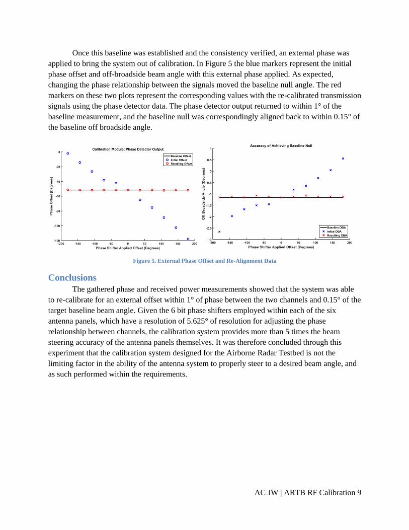
Once this baseline was established and the consistency verified, an external phase was
applied to bring the system out of calibration. In Figure 5 the blue markers represent the initial
phase offset and off-broadside beam angle with this external phase applied. As expected,
changing the phase relationship between the signals moved the baseline null angle. The red
markers on these two plots represent the corresponding values with the re-calibrated transmission
signals using the phase detector data. The phase detector output returned to within 1° of the
baseline measurement, and the baseline null was correspondingly aligned back to within 0.15° of
the baseline off broadside angle.
Figure 5. External Phase Offset and Re-Alignment Data
Conclusions
The gathered phase and received power measurements showed that the system was able
to re-calibrate for an external offset within 1° of phase between the two channels and 0.15° of the
target baseline beam angle. Given the 6 bit phase shifters employed within each of the six
antenna panels, which have a resolution of 5.625° of resolution for adjusting the phase
relationship between channels, the calibration system provides more than 5 times the beam
steering accuracy of the antenna panels themselves. It was therefore concluded through this
experiment that the calibration system designed for the Airborne Radar Testbed is not the
limiting factor in the ability of the antenna system to properly steer to a desired beam angle, and
as such performed within the requirements.

AC JW | ARTB RF Calibration 10
Table of Contents
Abstract ......................................................................................................................................................... 2
Statement of Authorship ............................................................................................................................... 3
Acknowledgements ....................................................................................................................................... 4
Executive Summary ...................................................................................................................................... 5
Introduction ............................................................................................................................................... 5
Methods .................................................................................................................................................... 6
Test Protocol ............................................................................................................................................. 7
Experimental Results ................................................................................................................................ 8
Conclusions ............................................................................................................................................... 9
Table of Contents ........................................................................................................................................ 10
Table of Figures .......................................................................................................................................... 12
1. Introduction ............................................................................................................................................. 14
2. Background ............................................................................................................................................. 16
2.1 Radar ................................................................................................................................................. 16
2.1.1 Electronically Steered Arrays .................................................................................................... 17
2.1.2 Time Delay Circuits versus Phase Shifters ................................................................................ 17
2.2 FIR Filtering ...................................................................................................................................... 19
2.2.1 Ideal Fractional Delay (FD) Filter ............................................................................................. 20
2.2.2 FD Filter Approximation ........................................................................................................... 21
2.3 Airborne Radar Testbed (ARTB) ...................................................................................................... 22
2.3.1 Mixer Theory ............................................................................................................................. 24
3. Methodology ........................................................................................................................................... 28
3.1 Design ............................................................................................................................................... 28
3.1.1 FPGA Design ............................................................................................................................. 29
3.1.2 Up-Converter ............................................................................................................................. 34
3.2 Verification of Test System .............................................................................................................. 37
3.2.1 FPGA Design Verification ......................................................................................................... 37
3.2.2 Upconverter Verification ........................................................................................................... 37
3.3 Measurement Techniques ................................................................................................................. 38

AC JW | ARTB RF Calibration 11
3.3.1 Calibration Waveforms .............................................................................................................. 39
3.3.2 Interferometer Broadside Null ................................................................................................... 40
3.3.3 MATLAB Controlled Measurement .......................................................................................... 41
3.4 Testing Calibration System ............................................................................................................... 42
3.4.1 Establish Baseline ...................................................................................................................... 42
3.4.2 Investigate Accuracy of Calibration Module ............................................................................. 43
3.5 Analysis............................................................................................................................................. 43
4. Results ..................................................................................................................................................... 44
4.1 Verification Results .......................................................................................................................... 44
4.2 Experimental Results ........................................................................................................................ 47
5. Discussion ............................................................................................................................................... 53
5.1 Implication of Results ....................................................................................................................... 53
5.2 Possible Data Concerns ..................................................................................................................... 53
5.2.1 Horizontal Linear Scan .............................................................................................................. 53
5.2.2 Multipath effects ........................................................................................................................ 55
6. Conclusions ............................................................................................................................................. 56
6.1 Measurement Conclusions ................................................................................................................ 56
6.2 Future Steps ...................................................................................................................................... 56
Works Cited ................................................................................................................................................ 58
Appendix A. MATLAB Code for Scanning Zaber Rail and Taking Block Measurements ...................... 59

AC JW | ARTB RF Calibration 12
Table of Figures
Figure 1. Sub-Array Waveform Generators .................................................................................................. 5
Figure 2. Overall system diagram showing FPGA hardware, upconverter and calibration RF components,
and horn antennas and power receiver for feedback loop ................................................................... 6
Figure 3. Calibration Waveform Theory ....................................................................................................... 7
Figure 4. Calibration Module Consistency Data ........................................................................................... 8
Figure 5. External Phase Offset and Re-Alignment Data ............................................................................. 9
Figure 6. Sub-array Waveform Generators (6 channels) ............................................................................ 15
Figure 7. Overview highlighting the general blocks utilized in radar ......................................................... 16
Figure 8. Five panel array using phase shifters for beam steering .............................................................. 17
Figure 9. Time delay beam steering additional distance to arrive .............................................................. 18
Figure 10. One dimensional phased array, split into k sub-arrays, with phase shifters at antenna elements
and time delay units driving each sub-array ...................................................................................... 19
Figure 11. Tapped Delay Line FIR Filter Implementation ......................................................................... 20
Figure 12. ARTB 6-panel antenna (bottom left) mounting plan. ................................................................ 22
Figure 13. ARTB calibration system (purple dotted box) components coupled prior to antenna system
(AESA) input. ................................................................................................................................... 23
Figure 14. Mixer Port Diagram ................................................................................................................... 24
Figure 15. Double Balanced Mixer Schematic ........................................................................................... 25
Figure 16. Impact of Bias Voltage on LO Square Wave ............................................................................ 26
Figure 17. Mixer Upconversion Operation ................................................................................................. 26
Figure 18. Overall system diagram showing FPGA hardware, upconverter and RF calibration
components, and horn antennas and power receiver for feedback loop ............................................ 29
Figure 19. FPGA block diagram inside box with UART cable for communication between MATLAB and
DAC peripheral for outputting waveforms ....................................................................................... 29
Figure 20. Finite phase stepped calibration waveform for “test” channel .................................................. 31
Figure 21. Magnitude response and group delay for 1/3 sample delay....................................................... 32
Figure 22. Single sample control module, shift register for five 16 sample sets. ....................................... 33
Figure 23. Upconverter Block Diagram ...................................................................................................... 34
Figure 24. Mixer upconversion images ....................................................................................................... 35
Figure 25. Upconverter Test Spectrogram .................................................................................................. 36
Figure 26. Calibration hardware in blue box with power dividers used to split transmitted signals, and sent
to phase detector and horn antennas .................................................................................................. 36
Figure 27. Spectrogram (top) and trace (bottom) of 600 MHz sine wave converted up to 16.8 GHz, shown
at peak of trace. ................................................................................................................................. 38
Figure 28. Picoscope three channel measurement setup ............................................................................. 39
Figure 29. Calibration waveform theory ..................................................................................................... 40
Figure 30. Power scan simulation for in-phase and interferometer measurements..................................... 41
Figure 31. Picoscope measurement of phase detector output (orange) triggered by master channel diode
detector (blue) ................................................................................................................................... 42
AC JW | ARTB RF Calibration 13
Figure 32. Waveform generation and transmission (left) with laptop, two VC707 board and RF
upconverter and calibration hardware in black chassis and feedback loop (right) with Zaber
Motorized Rail, two horn antennas and receiver antenna ................................................................. 44
Figure 33. Single period of FIR filtered output for 1/3 sample delay, no delay or advance and 1/3 sample
advance .............................................................................................................................................. 45
Figure 34. Spectrogram at 17.4 GHz (LO) center frequency with desired 16.8 GHz RF frequency (red)
and 16.2 GHz second-order spur (yellow) highly attenuated ..................................................................... 45
Figure 35. Oscilloscope wide view of synchronized FPGA outputs for 18µs waveform duration of master
(green) and slave (yellow) transmitted signals .................................................................................. 46
Figure 36. Close view (1ns/div) of phase aligned synchronization within 1ns between master (green) and
slave (yellow) transmitted signals ..................................................................................................... 46
Figure 37. Received power measurement to prove interferometer concept in test environment ................ 47
Figure 38. Baseline antenna pattern with broadside null at -1.16° off broadside angle .............................. 48
Figure 39. Baseline phase detector output over 1000 700 MHz calibration waveform measurements
resulting in a calculated phase offset of -51.683° ....................................................................................... 48
Figure 40. Baseline calculated transmit signal phase offset consistent within ~1° over 1000 measurements
........................................................................................................................................................... 49
Figure 41. Initial phase detector output as a result of external phase offset applied by phase shifter ........ 50
Figure 42. Initial power measurement as a result of external phase offset applied by phase shifter .......... 50
Figure 43. Phase detector calculated transmit signal offset over 11 distinct external phase offsets applied
by phase shifter ................................................................................................................................. 51
Figure 44. Comparison of initial null angle (blue) after applied phase shifter versus recalibrated null angle
(red) based on calibration phase offset data ...................................................................................... 52
Figure 45. Horizontal Linear Scan Measurement Distance vs. Curved Scan ............................................. 54
Figure 46. Overlaid return-to-baseline power scan measurements ............................................................. 55

AC JW | ARTB RF Calibration 14
1. Introduction The Airborne Radar Systems and Techniques group (Group 105) at MIT Lincoln
Laboratory has been developing an Airborne Radar Testbed (ARTB), a testing system that will
be placed on a Twin Otter aircraft, designed to facilitate end-to-end demonstrations of advanced
radar concepts and technologies for Intelligence, Surveillance, and Reconnaissance (ISR)
airborne radar research. The ARTB will be capable of testing current and advanced radar modes
such as GMTI, MMTI, SAR, ISAR, MIMO and EP1 with built-in flexibility for future modes. It
will collect raw data to aid algorithm development and demonstrate advanced RF and processing
concepts.
Radio Detection And Ranging (Radar) systems are tools for target location identification
which radiate electromagnetic waveforms and use the reflected energy to determine the position
and/or speed of the target. The radar antenna receives some of the echoed energy from the target,
and can amplify and process the returned signal to determine the location of the target in relation
to the antenna (Skolnik 1.1).
Initially, radar involved mechanically-steered dish antennas, the steering of which was
naturally restricted by the speed of motor and gimbal systems, and open to mechanical fatigue
and wear over time as a function of the cyclic loading. An electronically-steered antenna, on the
other hand, utilizes an individual electronic device behind each antenna element, which can
manipulate the time delay or phase of the signal passing through it. With a computer controlling
each element simultaneously, the overall beam direction and its shape can be digitally controlled
rather than relying on mechanically steering the beam.
The antenna system implemented in the ARTB is comprised of Active Electronically-
Scanned Arrays (AESAs). AESAs utilize phase shifters as opposed to time delay circuits for
beam steering; phase shifters are more appealing than time delay circuits because of size,
complexity and cost. The main difference is that time delay circuits receive the transmitted signal
from a single high-power transmitter source and selectively delay a portion of the RF signal in
order to form and steer the beam. In the case of phase shifters, each antenna element has its own
transmit/receive module employing a phase shifter which receives a digital “command” telling
the element how to delay the signal to form a particular beam. However, utilizing phase shifter
beamforming over wide instantaneous bandwidths produces beam squint impacting the accuracy
of the beam significantly. Beam squint refers to the case that over different frequencies, the
actual beam angle progressively drifts from the expected beam angle. To combat this inaccuracy,
the antenna system employed on the ARTB consists of six sub-array panels in series. Within
each sub-array, the antenna elements still use phase shifters for steering. However, each sub-
array panel is driven by a unique RF waveform generator as illustrated in Figure 6, allowing for
1 GMTI refers to ground moving target indicator radar; MMTI refers to maritime moving target indicator; SAR and ISAR refer to synthetic aperture radar, utilized for airborne and spaceborne radar; MIMO refers to multiple input and multiple output radar; and EP refers to electronic protection.
AC JW | ARTB RF Calibration 15
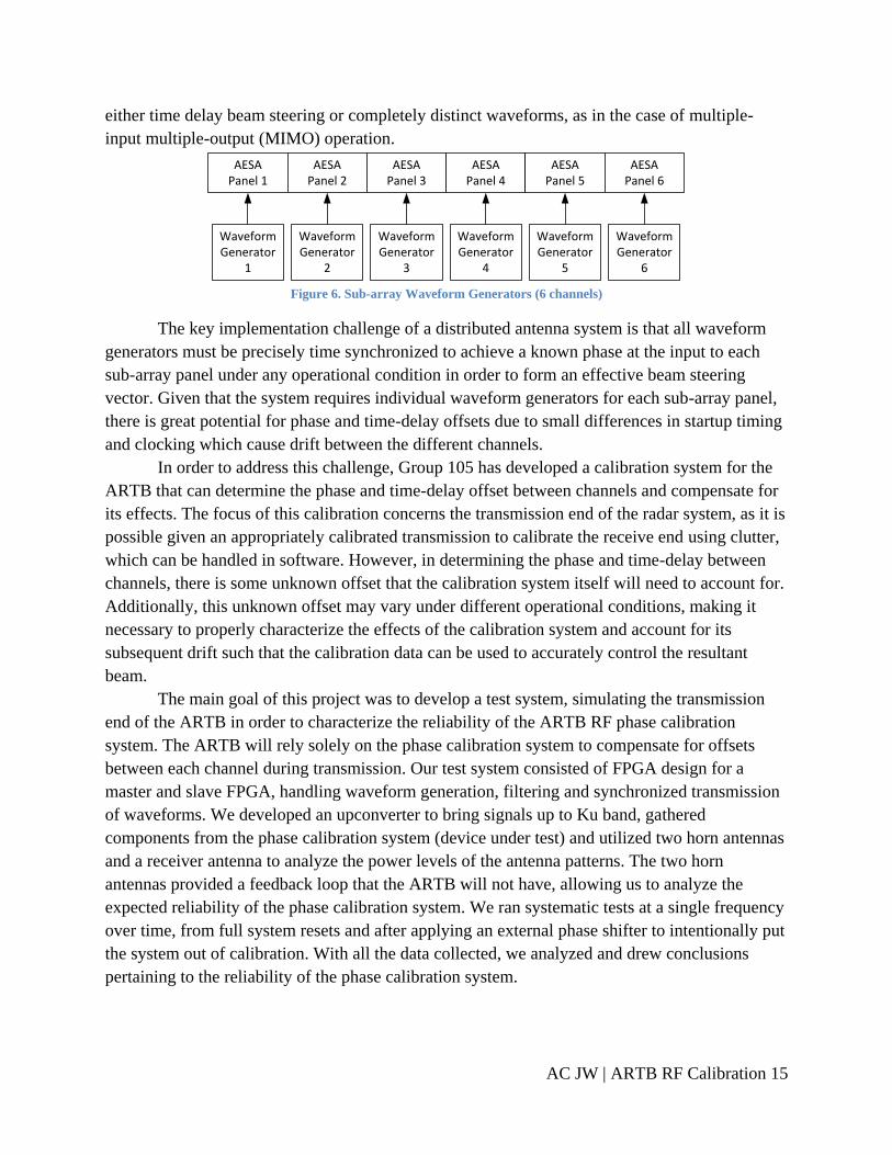
either time delay beam steering or completely distinct waveforms, as in the case of multiple-
input multiple-output (MIMO) operation.
AESAPanel 1
AESAPanel 2
AESAPanel 3
AESAPanel 4
AESAPanel 5
AESAPanel 6
Waveform Generator
1
Waveform Generator
2
Waveform Generator
3
Waveform Generator
4
Waveform Generator
5
Waveform Generator
6
Figure 6. Sub-array Waveform Generators (6 channels)
The key implementation challenge of a distributed antenna system is that all waveform
generators must be precisely time synchronized to achieve a known phase at the input to each
sub-array panel under any operational condition in order to form an effective beam steering
vector. Given that the system requires individual waveform generators for each sub-array panel,
there is great potential for phase and time-delay offsets due to small differences in startup timing
and clocking which cause drift between the different channels.
In order to address this challenge, Group 105 has developed a calibration system for the
ARTB that can determine the phase and time-delay offset between channels and compensate for
its effects. The focus of this calibration concerns the transmission end of the radar system, as it is
possible given an appropriately calibrated transmission to calibrate the receive end using clutter,
which can be handled in software. However, in determining the phase and time-delay between
channels, there is some unknown offset that the calibration system itself will need to account for.
Additionally, this unknown offset may vary under different operational conditions, making it
necessary to properly characterize the effects of the calibration system and account for its
subsequent drift such that the calibration data can be used to accurately control the resultant
beam.
The main goal of this project was to develop a test system, simulating the transmission
end of the ARTB in order to characterize the reliability of the ARTB RF phase calibration
system. The ARTB will rely solely on the phase calibration system to compensate for offsets
between each channel during transmission. Our test system consisted of FPGA design for a
master and slave FPGA, handling waveform generation, filtering and synchronized transmission
of waveforms. We developed an upconverter to bring signals up to Ku band, gathered
components from the phase calibration system (device under test) and utilized two horn antennas
and a receiver antenna to analyze the power levels of the antenna patterns. The two horn
antennas provided a feedback loop that the ARTB will not have, allowing us to analyze the
expected reliability of the phase calibration system. We ran systematic tests at a single frequency
over time, from full system resets and after applying an external phase shifter to intentionally put
the system out of calibration. With all the data collected, we analyzed and drew conclusions
pertaining to the reliability of the phase calibration system.

AC JW | ARTB RF Calibration 16
2. Background This chapter outlines the background information required to understand the development
of our test system. First, we provide a general overview of radar, then highlight the theory and
need behind development of a system for calibrating the RF calibration system on the Airborne
Radar Testbed, providing an overview of the testbed itself, along with the radar techniques that it
employs. Lastly, it delves deeper into a vital component of the project, the RF mixer, which was
used for both frequency conversion to Ku band and phase detection.
2.1 Radar
Radar is an electromagnetic sensor for the detection of reflecting objects and can be
broken up into four main subsystems as illustrated in Figure 7: transmitter, antenna, receiver and
signal processor/data processing block.
Figure 7. Overview highlighting the general blocks utilized in radar
The transmitter generates a suitable waveform for the particular functionality the radar is
to serve. The antenna is the device that allows the transmitted energy to be propagated into space
and then collects the echo energy on receive; it is almost always a directive antenna, one that
directs the radiated energy into a narrow beam to concentrate the power as well as to allow the
determination of the direction to the target. The receiver amplifies the weak received signal to a
level where its presence can be detected. The signal processor might be described as being the
part of the receiver that separates the desired signal from the undesired signals that can degrade
the detection process. Given that radar can (generally) be broken up into these four main
subsystems, it is evident that there is no single way to characterize radar. One major feature,
however, that distinguishes one type of radar from another is its antenna system. The antenna can
be mechanically scanned or electronically scanned to form and steer the beam; each type of
antenna has its particular advantages and limitations.

AC JW | ARTB RF Calibration 17
2.1.1 Electronically Steered Arrays
The first generation of radar involved mechanically-steered dish antennas that were
naturally restricted by the speed of motor and gimbal systems, and open to mechanical fatigue
and wear over time as a function of the cyclic loading. By the 1970s, radar technology shifted to
mechanically-steered planar arrays; instead of steering the beam by reflection as dish antennas
do, planar arrays manipulate individual time delays into a number of antenna elements
(radiators), arranged in a planar array panel. Regardless, mechanically-steered planar arrays still
held heavy reliance on servomotors and gimbals that not only take a (relatively) long amount of
time to steer the antenna but also suffer from fatigue applied to the components over the course
of its operational time.
Phased array radars can be electrically steered, providing a faster means of beam steering
and increased flexibility as the capability of rapidly and accurately switching beams permits
multiple radar functions to be performed (Skolnik 13.1). Electronically steered arrays (ESAs)
typically utilize time delay circuits or phase scanning to achieve beam steering.
2.1.2 Time Delay Circuits versus Phase Shifters
Beam steering can be achieved by applying the desired phase shift using phase shifters,
or applying time delays which produce a frequency dependent phase shift. Consider a uniformly
spaced five element linear array, depicted in Figure 8. Adjusting the phase of the signal
transmitted by each element allows the collective signals to act as the signal of a single antenna,
effectively forming the beam and allowing for adjustments to steer the beam as well.
Figure 8. Five panel array using phase shifters for beam steering
By controlling the phase and amplitude of excitation to each element, the beam shape and
direction can be controlled. The phase excitation controls the beam angle of the radiated pattern
from the array. For example, to produce a broadside beam, θ0 = 0°, the phase excitation for all
elements would be ϕ0 = 0°. Other scan angles would require a phase excitation corresponding to
equation 1.
𝛟(𝐧) =𝟑𝟔𝟎° ∗ 𝒅∗𝒏 ∗𝒔𝒊𝒏(𝛉)
𝝀 (1)

AC JW | ARTB RF Calibration 18
where n = the nth element, d = the spacing between each antenna element (meters), θ = the
desired beam angle (°) and 𝜆 =𝑐
𝑓 where c is the velocity of propagation (speed of light: 3*10
8
m/s) and f is the frequency of the wave (Hz). If the phase shift at each element n, ϕ(n), is fixed,
the scan angle θ becomes frequency-dependent given that wavelength λ is dependent on
frequency. The change in scan angle θ as a result of change in frequency highlights the concept
of beam squint, a disadvantage of phase shifters.
On the contrary, time-delay beam steering is frequency-independent; time delay units
provide true time delay. For a signal transmitted at a beam angle of θ°, then according to the
geometry in Figure 9 the wave must travel an additional distance d*sin(θ) to maintain the beam
angle.
Figure 9. Time delay beam steering additional distance to arrive
Assuming the same five panel array as shown in Figure 8 with time delay circuits instead of
phase shifters, the required incremental time delay at each time delay uint, t(n), to achieve a
beam angle θ is shown in a similar equation 2:
𝒕(𝒏) =𝒅∗𝒏∗𝐬𝐢𝐧 (𝛉𝟎)
𝒄 (2)
where n = the nth element, d = the spacing between each antenna element (meters), θ0 = the
desired beam angle (°) and c = the velocity of propagation (speed of light: 3*108 m/s). The issue
is that individual time-delay circuits are normally too cumbersome and impractical to be added to
each radiating element (Longbrake). Phase shifters are prevalent, appealing in size, complexity
and cost, but are frequency independent. Without true time delay, for wide instantaneous
bandwidth signals, the beam will distort (squint) over frequency. Beam squint can be enough to
steer the beam entirely off the target, resulting in a greatly reduced collected (received) signal.
To combat beam squint, the use of time delay circuits can provide true time delay beam
steering. Essentially, the antenna elements of the phased array can be grouped together into a
series of sub-arrays where time-delay circuits drive each sub-array, as illustrated in Figure 10.
dsin(θ°)
AC JW | ARTB RF Calibration 19
Figure 10. One dimensional phased array, split into k sub-arrays, with phase shifters at antenna elements and time delay
units driving each sub-array
Dividing the phased array into a sub-arrays mitigates (but does not eliminate) the beam
squint problem; each sub-array of phase shifters will have the same beam squint issue but not
nearly as significantly as the beam squint that would be exhibited in a solely phase-steered array.
The time delay control for each sub-array allows for true time delay beam steering of the whole
antenna system. Time delay control can be achieved using switched microwave or optical
networks (coaxial cables, etc.) or digital sampling and signal processing (filtering) such as a
unique waveform generator for each channel (D-REX).
2.2 FIR Filtering
Finite Impulse Response (FIR) filters are generally used to attenuate the magnitude of a
signal in a desired way depending on the signal’s frequency. The four most common FIR filters
are lowpass, highpass, bandpass, and notch filters. The basic structure to implement an FIR filter
is a tapped delay line, in which a series of delays, multipliers and adders create the desired result.
FIR filters are designed by selecting the set of coefficients, a(0) through a(N-1) where N is the
order of the filter, which act as the values used by the multipliers. This basic structure is shown
in Figure 11, and is represented by equation 3.
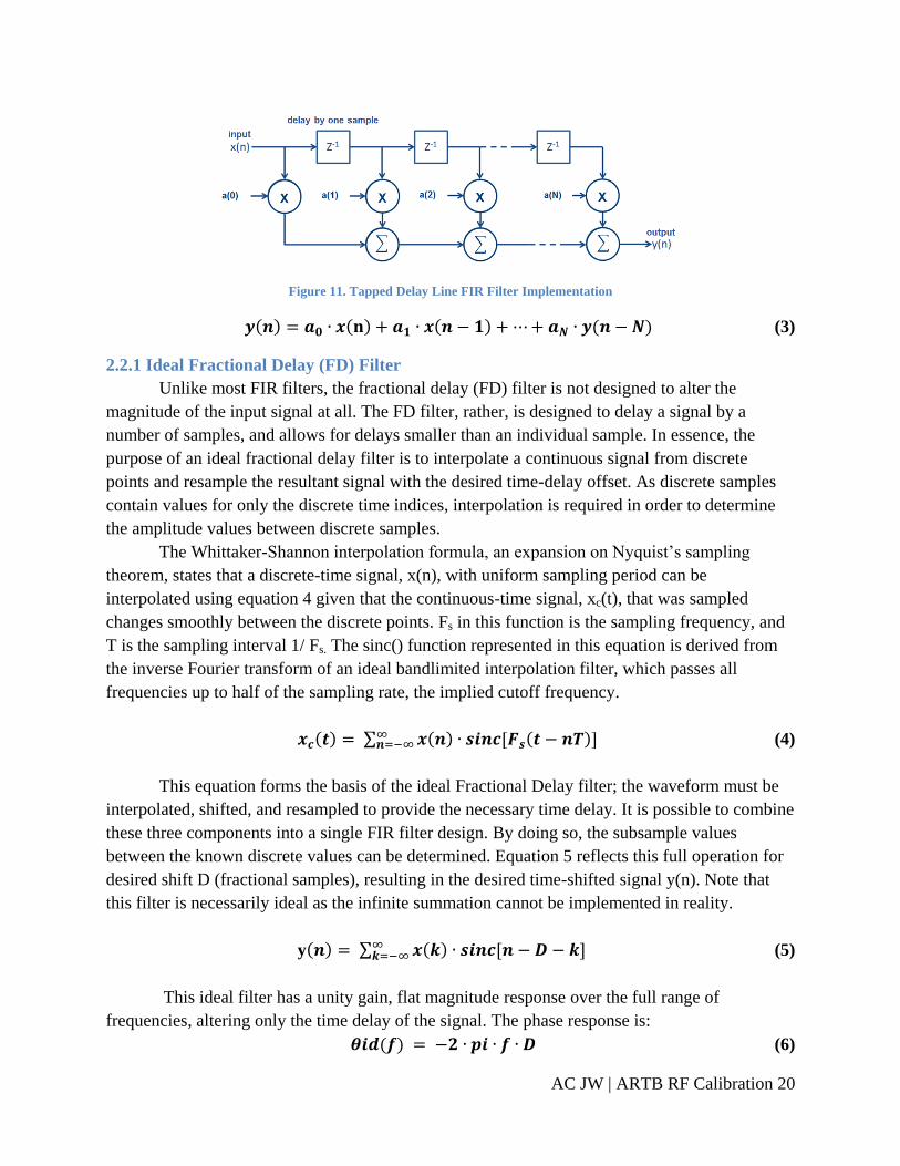
AC JW | ARTB RF Calibration 20
Figure 11. Tapped Delay Line FIR Filter Implementation
𝒚(𝒏) = 𝒂𝟎 ∙ 𝒙(𝐧) + 𝒂𝟏 ∙ 𝒙(𝒏 − 𝟏) + ⋯ + 𝒂𝑵 ∙ 𝒚(𝒏 − 𝑵) (3)
2.2.1 Ideal Fractional Delay (FD) Filter
Unlike most FIR filters, the fractional delay (FD) filter is not designed to alter the
magnitude of the input signal at all. The FD filter, rather, is designed to delay a signal by a
number of samples, and allows for delays smaller than an individual sample. In essence, the
purpose of an ideal fractional delay filter is to interpolate a continuous signal from discrete
points and resample the resultant signal with the desired time-delay offset. As discrete samples
contain values for only the discrete time indices, interpolation is required in order to determine
the amplitude values between discrete samples.
The Whittaker-Shannon interpolation formula, an expansion on Nyquist’s sampling
theorem, states that a discrete-time signal, x(n), with uniform sampling period can be
interpolated using equation 4 given that the continuous-time signal, xc(t), that was sampled
changes smoothly between the discrete points. Fs in this function is the sampling frequency, and
T is the sampling interval 1/ Fs. The sinc() function represented in this equation is derived from
the inverse Fourier transform of an ideal bandlimited interpolation filter, which passes all
frequencies up to half of the sampling rate, the implied cutoff frequency.
𝒙𝒄(𝒕) = ∑ 𝒙(𝒏) ∙ 𝒔𝒊𝒏𝒄[𝑭𝒔(𝒕 − 𝒏𝑻)]∞𝒏=−∞ (4)
This equation forms the basis of the ideal Fractional Delay filter; the waveform must be
interpolated, shifted, and resampled to provide the necessary time delay. It is possible to combine
these three components into a single FIR filter design. By doing so, the subsample values
between the known discrete values can be determined. Equation 5 reflects this full operation for
desired shift D (fractional samples), resulting in the desired time-shifted signal y(n). Note that
this filter is necessarily ideal as the infinite summation cannot be implemented in reality.
y(𝒏) = ∑ 𝒙(𝒌) ∙ 𝒔𝒊𝒏𝒄[𝒏 − 𝑫 − 𝒌]∞𝒌=−∞ (5)
This ideal filter has a unity gain, flat magnitude response over the full range of
frequencies, altering only the time delay of the signal. The phase response is:
𝜽𝒊𝒅(𝒇) = −𝟐 ∙ 𝒑𝒊 ∙ 𝒇 ∙ 𝑫 (6)

AC JW | ARTB RF Calibration 21
The response represented here results in both phase delay and group delay constant and equal to
D.
Although FD filters have linear phase response and constant phase delay, they are not
traditionally considered linear-phase as the impulse response is asymmetric about the center
point. Rather, the FD filter has "generalized linear phase” for the desired passband.
Unfortunately, it is impossible to realize an ideal FD filter in reality. When the desired
delay is integer-valued (ie. the delay does not have a fractional component), the sinc() function is
zero for every point other than at the center point, but for subsample delay the impulse response
is infinite in duration, as the sampled sinc() function used for interpolation is infinitely long in
both directions. As this discrete impulse response is infinitely long in both directions, the ideal
filter must be non-causal for fractional delays and would have an infinite duration impulse
response. Therefore, the ideal FD filter is impossible to create in reality.
2.2.2 FD Filter Approximation
The most intuitive method for approximating the ideal FD filter is to simply truncate the
impulse response symmetrically about the midpoint such that it is not infinitely long in both
directions. A side effect of such a truncation is frequency response ripple, referred to as Gibbs
Phenomenon. Essentially, the discontinuity created by the truncation of the filter causes
overshoot and ringing in the frequency domain.
There are a few different options for minimizing the effects of Gibbs Phenomenon. One
could use a lowpass interpolator instead of a fullband fractional delay filter or use a reduced
bandwidth with a smooth transition band function, for example. Both of these options result in a
decreased bandwidth, but also decrease the amount of ripple.
Another solution is to employ a time-domain window function to provide a smooth
transition to 0. As seen in this equation, the sinc function is simply multiplied by the windowing
function to result in the desired response2 (Poornachandra and Sasikala 7.5). Note that the
windowing function w(n - D) must drop-off to 0 on both sides to adequately remove the infinite
sum issue, and must also be offset by D to preserve the desired filter characteristic. Equation 7
represents the impulse response of an FD filter designed with a windowing function approach.
𝒉(𝒏) = {𝒘(𝒏 − 𝑫) ∙ 𝒔𝒊𝒏𝒄(𝒏 − 𝑫), 𝒇𝒐𝒓 𝟎 ≤ 𝒏 < 𝑵
𝟎, 𝒐𝒕𝒉𝒆𝒓𝒘𝒊𝒔𝒆 (7)
For the filters designed for this project, a truncated Taylor window was applied in
MATLAB to the coefficient set. This window is an approximation of a Dolph-Chebyshev
window which allows the Dolph-Chebyshev sidelobe ripples to drop off at the edges in the time
domain, avoiding edge discontinuities, and can be expressed as:
2 This is the impulse response of the filter, and as such does not include x(n). The infinite summation is removed by
the window which is 0 for all points outside of the desired filter order.

AC JW | ARTB RF Calibration 22
𝒘(𝒕) = {(𝟏+𝒌)
𝟐+
(𝟏−𝒌)
𝟐𝐜𝐨𝐬 (
𝝅𝒕
𝝉) , 𝒇𝒐𝒓 |𝒕| ≤ 𝝉
𝟎, 𝒐𝒕𝒉𝒆𝒓𝒘𝒊𝒔𝒆 (8)
where k is a value in the range of 0 ≤ k ≤ 1 (Prabhu 5.2.5).
. The number of sidelobes and the sidelobe attenuation were two significant factors that
had to be adjusted such that the filter maintained an appropriate bandwidth while still properly
mitigating the ringing from Gibbs Phenomenon.
2.3 Airborne Radar Testbed (ARTB)
The ARTB will be mounted on a Twin Otter aircraft as illustrated in Figure 12 in order to
facilitate end-to-end demonstrations of advanced radar concepts and technologies. The ARTB
will be implemented in two phases; phase-1 encompasses an antenna system operating at Ku3
band single polarity with 6 channels; phase-2 expands to a 12 channel antenna system capable of
operating at X4-Ku dual band.
Figure 12. ARTB 6-panel antenna (bottom left) mounting plan.
System analysis indicates that the ARTB can achieve high radar performance in the
expected operating environment with respect to handling clutter, platform motion, vibration and
jamming. The Twin Otter aircraft will be modified in order to fit all blocks of the ARTB such as
the AESA antenna system strong back (casing), digital receiver/exciter (D-REX) and processor
to handle transmission and receiving signals, RF receiver/exciter and lastly data storage.
There are potential limiting factors of the ARTB, however. A primary concern is that
there will naturally be some phase offset between each channel stemming from random
fluctuations in phase of the local oscillator, plus additional contributions from digital-to-analog
3 Ku band (12-18 GHz) 4 X band (8-12 GHz)
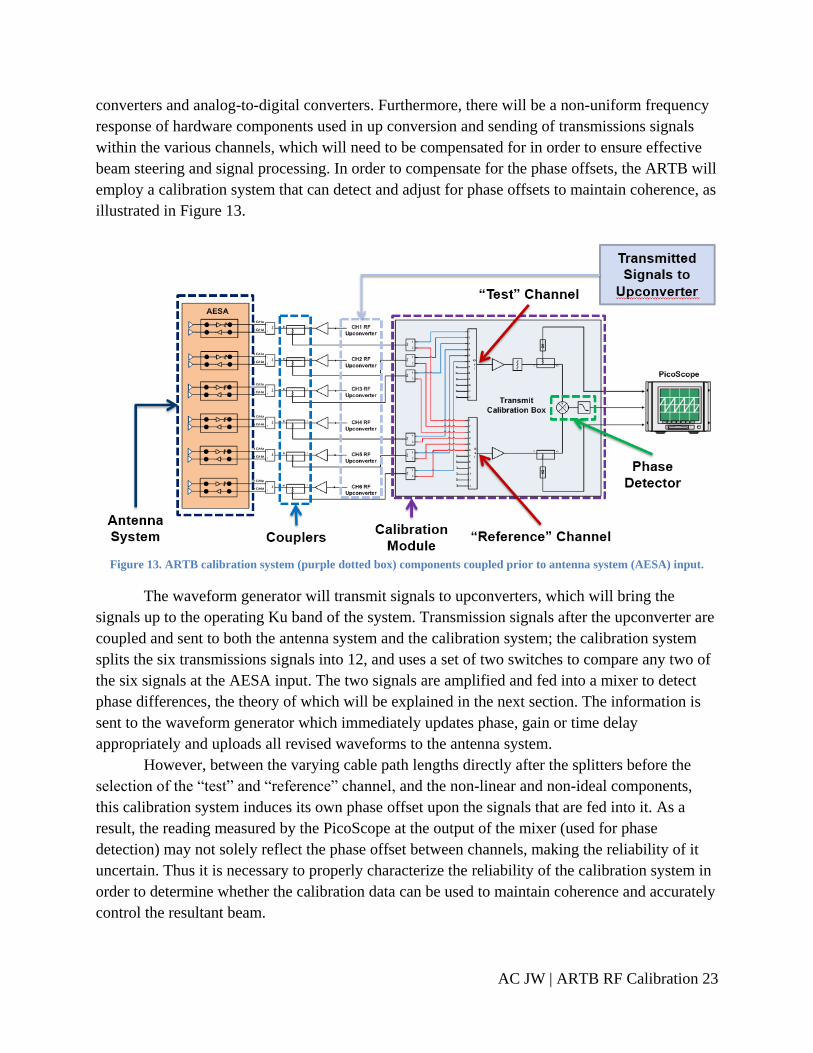
AC JW | ARTB RF Calibration 23
converters and analog-to-digital converters. Furthermore, there will be a non-uniform frequency
response of hardware components used in up conversion and sending of transmissions signals
within the various channels, which will need to be compensated for in order to ensure effective
beam steering and signal processing. In order to compensate for the phase offsets, the ARTB will
employ a calibration system that can detect and adjust for phase offsets to maintain coherence, as
illustrated in Figure 13.
Figure 13. ARTB calibration system (purple dotted box) components coupled prior to antenna system (AESA) input.
The waveform generator will transmit signals to upconverters, which will bring the
signals up to the operating Ku band of the system. Transmission signals after the upconverter are
coupled and sent to both the antenna system and the calibration system; the calibration system
splits the six transmissions signals into 12, and uses a set of two switches to compare any two of
the six signals at the AESA input. The two signals are amplified and fed into a mixer to detect
phase differences, the theory of which will be explained in the next section. The information is
sent to the waveform generator which immediately updates phase, gain or time delay
appropriately and uploads all revised waveforms to the antenna system.
However, between the varying cable path lengths directly after the splitters before the
selection of the “test” and “reference” channel, and the non-linear and non-ideal components,
this calibration system induces its own phase offset upon the signals that are fed into it. As a
result, the reading measured by the PicoScope at the output of the mixer (used for phase
detection) may not solely reflect the phase offset between channels, making the reliability of it
uncertain. Thus it is necessary to properly characterize the reliability of the calibration system in
order to determine whether the calibration data can be used to maintain coherence and accurately
control the resultant beam.
AC JW | ARTB RF Calibration 24
2.3.1 Mixer Theory
A radio-frequency (RF) mixer is an active or passive three port device as illustrated in
Figure 14 that, at a basic level, multiplies two different sinusoidal input signals (IF, LO) together
to produce the output (RF). The cosine product identity described by equation 8 shows that an
ideal multiplication will result in two different frequencies, the sum and difference, of the two
input frequencies given two sinusoidal inputs.
Figure 14. Mixer Port Diagram
𝑰𝑭 ∗ 𝑳𝑶 = 𝑹𝑭 = 𝒄𝒐𝒔(𝝎𝟏𝒕)𝒄𝒐𝒔( 𝝎𝟐𝒕) =𝒄𝒐𝒔(𝝎𝟏𝒕−𝝎𝟐𝒕)+𝒄𝒐𝒔(𝝎𝟏𝒕+ 𝝎𝟐𝒕)
𝟐 (8)
For the purposes of this project, this mixer multiplication is employed for both frequency
conversion and phase detection.
2.3.1.1 Double Balanced Mixer Operation
The double-balanced mixer, as illustrated in Figure 15, is a common mixer used in both
frequency conversion and phase detection. There are other mixer designs in common use, but the
double-balanced mixer has been chosen for this explanation specifically as it supports use as a
phase detector. For the purpose of explaining the operation of the double-balanced mixer, we
will observe the operation when the LO and RF ports are used as inputs and the IF port is the
output signal. The mixer is not always used in this configuration, as for frequency up-conversion
the RF port acts as the output and the LO and IF ports are inputs, but the behavior is similar.

AC JW | ARTB RF Calibration 25
Figure 15. Double Balanced Mixer Schematic
To begin, the center-tapped transformer T1 is employed to create a differential signal
from the single-ended local oscillator (LO). The diode ring essentially transforms this differential
sinusoidal signal into a square wave. When the differential LO is positive, current flows through
diodes D4 and D3. When these diodes are conducting, a virtual ground is created between these
two diodes, as the voltage is being split evenly between them and the center-tap of the
transformer T1 is tied to ground. At the same time, diodes D1 and D2 are not conducting, and
can be simplified to open circuits. With D1 and D2 not conducting, one end of the transformer
T2 (4) is left open-circuited and the other (6) connected to virtual ground. As a result, the
application of a separate signal to the RF port passes to the IF port. Assuming a transformer turn
ratio of 2:1, this signal passes through with minimal attenuation. When the differential LO signal
is negative, on the other hand, diodes D1 and D2 conduct, and D3 and D4 act as open circuits.
This configuration results in a situation where the opposite end of transformer T2 (6) is left open-
circuited and the other (4) connected to virtual ground. Essentially, this configuration results in
an inversion of the RF signal passing through to the IF port. In short, the resultant IF signal is the
modulation of the RF signal with a square wave at the LO frequency. When the differential LO
signal is positive, the RF input passes to the IF output normally; but when it is negative, the RF
input is negated before being output to the IF port. Thus the full-wave multiplication is achieved.
This physical explanation is necessarily a simplification of the process which occurs
within a double-balanced mixer, as a diode does not operate perfectly like an ideal switch. Non-
linear behavior within the diodes affects the output signal and generates additional spurious
frequencies beyond the two first-order images. This explanation also does not take into
consideration the bias voltage of the diodes, which both decreases the magnitude of the
modulating square wave, and introduces a transition interval where neither set of diodes is
conducting (as shown in Figure 16), leaving both ends of the transformer open-circuited.
AC JW | ARTB RF Calibration 26
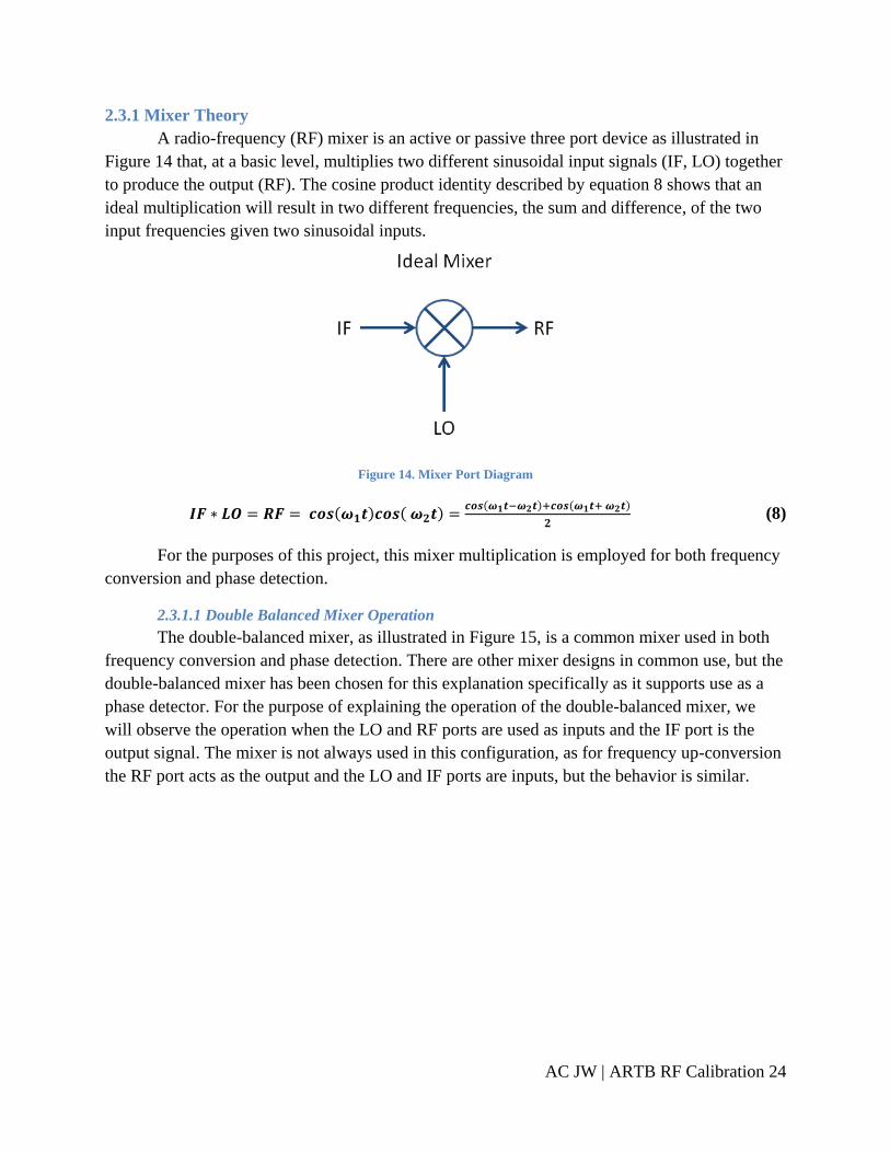
Figure 16. Impact of Bias Voltage on LO Square Wave
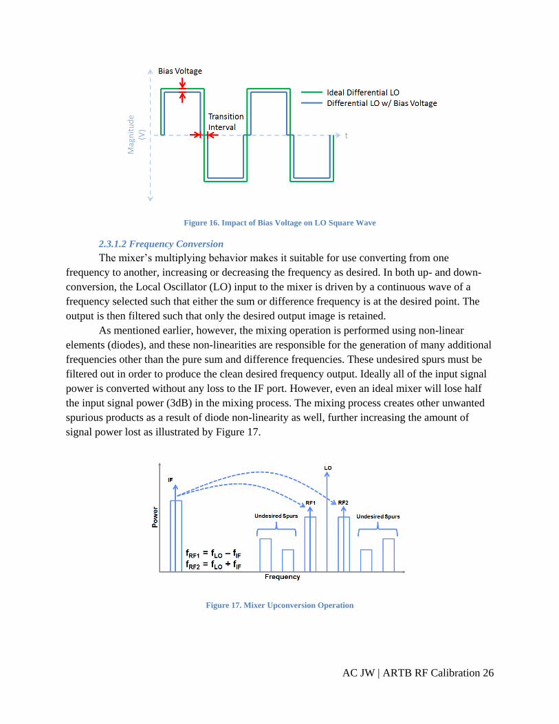
2.3.1.2 Frequency Conversion
The mixer’s multiplying behavior makes it suitable for use converting from one
frequency to another, increasing or decreasing the frequency as desired. In both up- and down-
conversion, the Local Oscillator (LO) input to the mixer is driven by a continuous wave of a
frequency selected such that either the sum or difference frequency is at the desired point. The
output is then filtered such that only the desired output image is retained.
As mentioned earlier, however, the mixing operation is performed using non-linear
elements (diodes), and these non-linearities are responsible for the generation of many additional
frequencies other than the pure sum and difference frequencies. These undesired spurs must be
filtered out in order to produce the clean desired frequency output. Ideally all of the input signal
power is converted without any loss to the IF port. However, even an ideal mixer will lose half
the input signal power (3dB) in the mixing process. The mixing process creates other unwanted
spurious products as a result of diode non-linearity as well, further increasing the amount of
signal power lost as illustrated by Figure 17.
Figure 17. Mixer Upconversion Operation

AC JW | ARTB RF Calibration 27
2.3.1.3 Phase Detection
By the same process as the up-conversion/down-conversion mixing action, an RF mixer
can be used to determine the phase difference between two different input signals if both of the
input signals have the same frequency. For instance, if the signals applied to the RF and LO ports
of a mixer have the same frequency ω and arbitrary phase φ, then it can be shown that, in the
ideal case where the mixer operates as a pure multiplier, the resultant IF voltage will be:
𝑽𝒐 = 𝒄𝒐𝒔(𝝎𝒕) ∗ 𝒄𝒐𝒔(𝝎𝒕 + 𝝋) (9)
Using the trigonometric identity,
𝑽𝒐 = 𝒄𝒐𝒔(𝝎𝒕) ∗ 𝒄𝒐𝒔(𝝎𝒕 + 𝝋) =𝒄𝒐𝒔(𝝋)+𝒄𝒐𝒔(𝟐𝝎𝒕+𝝋)
𝟐 (10)
Using a lowpass filter to remove the 2ωt term, the output voltage will become:
𝑽𝒐 =𝒄𝒐𝒔(𝝋)
𝟐 (11)
As shown, the output voltage becomes a DC voltage related directly to the phase offset
between the two input signals at the RF and LO ports; the output will vary as a cosine of the
phase difference between the input signals making the phase offset easily derivable. Ideally when
φ = π/2 the DC voltage output at the IF port should be zero. It is worth noting that this result
reflects an inherent phase ambiguity stemming from different phase offsets corresponding to the
same output voltage, i.e. cos(φ) = cos(-φ). The phase ambiguity must be mitigated somehow in
the implementation phase of a mixer as a phase detector. This phase detector application is
employed by the ARTB’s calibration system, the unit under test.

AC JW | ARTB RF Calibration 28
3. Methodology The goal of this project investigates and characterizes the calibration system of the
ARTB. Specifically, we set five main objectives to achieve: (1) design and develop a system
simulating the ARTB transmission, (2) verify that the system achieves functionality, (3) develop
measurement techniques to use when testing, (4) test the calibration system of the ARTB for
consistency and performance at a single frequency using two horn antennas and a receiver
antenna as a feedback loop, and (5) analyze the experimental data to quantify the consistency and
accuracy of the calibration unit and explore any resulting implications about the device under
test.
3.1 Design
The calibration system of the ARTB was the Device under Test (DUT) of our project. In
order to isolate and characterize the calibration system, it was necessary to develop a system
simulating the radar transmission employed on the testbed. Transmission for the system involved
the creation of hardware and software for signal generation, phase alignment, transmission and
radiation. To perform the transmission operations, FPGA hardware on two Virtex VC707
Evaluation Boards was developed to accept generated signals from MATLAB, adjust the relative
phase of the signals, and transmit single frequency signals using a DAC. An upconverter was
employed that was designed prior to the start of the project, and the resulting RF signal was
transmitted via a pair of horn antennas. A power receiver captured the antenna patterns for an
additional feedback loop allowing for measuring accuracy. All measurements were captured by a
Picoscope controlled through MATLAB. An overall system diagram is illustrated in Figure 18.
AC JW | ARTB RF Calibration 29
Figure 18. Overall system diagram showing FPGA hardware, upconverter and RF calibration components, and horn
antennas and power receiver for feedback loop
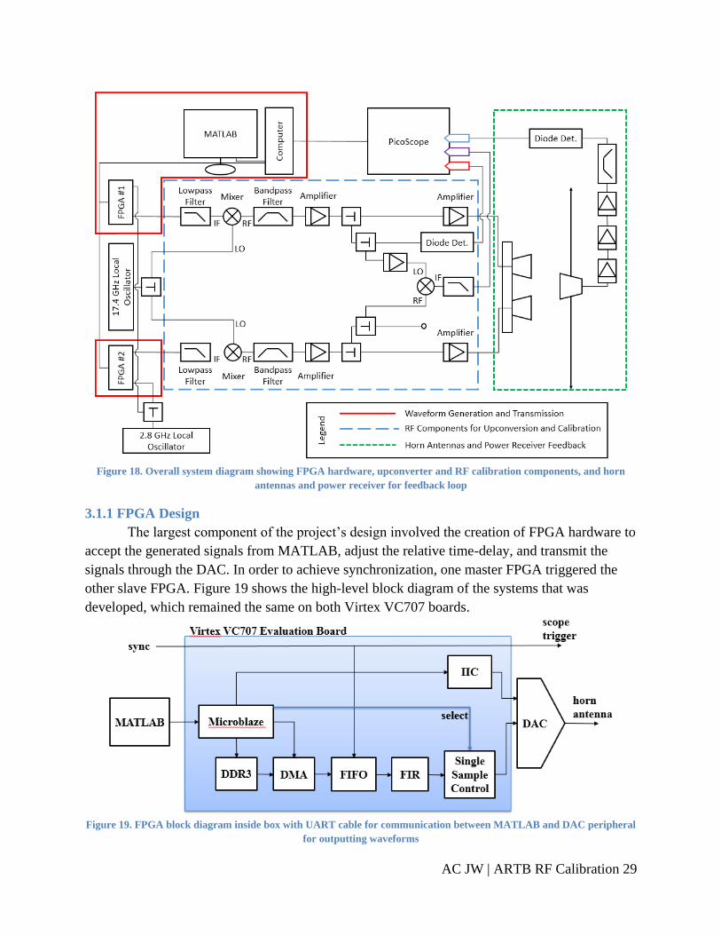
3.1.1 FPGA Design
The largest component of the project’s design involved the creation of FPGA hardware to
accept the generated signals from MATLAB, adjust the relative time-delay, and transmit the
signals through the DAC. In order to achieve synchronization, one master FPGA triggered the
other slave FPGA. Figure 19 shows the high-level block diagram of the systems that was
developed, which remained the same on both Virtex VC707 boards.
Figure 19. FPGA block diagram inside box with UART cable for communication between MATLAB and DAC peripheral
for outputting waveforms

AC JW | ARTB RF Calibration 30
The FPGA hardware design fulfills three primary functions, the reception and storage of
pre-generated waveforms, the addition of programmable delay to match the signals output by
two different FPGAs, and the transmission via DAC. The reception and storage of the
waveforms is accomplished via Universal Asynchronous Receiver/Transmitter (UART)
transmission from MATLAB through the Microblaze, storage in DDR3 SDRAM, and a Direct
Memory Access (DMA) block. A FIFO is used as a buffer to preload data from DDR3 memory
in order to ensure throughput. The FIR FD and Single Sample Control filter blocks add the
necessary delay, with subsample and single sample resolution, respectively. The DAC is
controlled via an IIC interface. The design is then synchronized between two VC707 evaluation
boards such that the waveforms can be transmitted to two different horn antennas. The two
evaluation boards run simultaneously, each with the same implemented hardware design. As the
DAC output defines the requirements for the rest of the system, we will first begin with an
explanation of how signals are being sent from the FPGA, and will follow with a description of
the system in place to meet those requirements within the chip.
3.1.1.1 Waveform Reception and Storage
The FPGA system was designed to accept any type of waveform from MATLAB such
that new data could be transmitted via the antennas during the test if needed. These test
waveforms take two main forms: continuous waves and calibration waveforms. Continuous
waves are sine waves at specific frequencies that transmit indefinitely. The functionality was
important for the experiment to account for the fact that the power receiver would take a given
amount of time to scan and record the beam pattern radiated by the antennas. The second type of
data used for the experiment was a finite calibration waveform. As seen in Figure 20, the
calibration waveform consists of a series of “chips”: contiguous 1μs sinusoids over the set of
sample frequencies. At each frequency, four of these chips were transmitted with 90° phase
offset intervals so that four phase measurements could be taken (at the DUT) for each frequency.
The four phase differences were sent to account for DC offset at the detector and alleviate phase
ambiguity in the measurement. The method by which the detector offset and phase ambiguity is
determined is further explained in Section 3.3.1. For the purposes of testing the ARTB
calibration system, nine frequencies were employed in the calibration waveform, ranging from
16.6 to 17 GHz (MATLAB generated 400-800 MHz IF) in intervals of 50 MHz. Therefore, the
value of N in Figure 20 is nine, and the total length of the calibration waveform is 37μs.

AC JW | ARTB RF Calibration 31
Figure 20. Finite phase stepped calibration waveform for “test” channel
Once generated, these 16-bit unsigned integer waveforms were transmitted via a serial Universal
Asynchronous Receiver/Transmitter (UART) port directly from MATLAB to the FPGA. The
MicroBlaze microcontroller within the FPGA stored the waveform data in DDR3 SDRAM on
the VC707 evaluation board. The Microblaze then signaled a Direct Memory Access (DMA)
block to begin data buffering. Before being sent through the time-delay circuitry, the data passed
through a data FIFO (First-In-First-Out Buffer) which buffered the data and waited for a
synchronization pulse to begin the actual transmission.
3.1.1.2 Time Delay – FIR Filter and Single Sample Control
As outlined in the background section of our report, sub-sample time delay control was
achieved using Fractional Delay (FD) FIR filters. The filters generated via MATLAB using the
process described in that section were loaded into a reloadable FIR filter within the FPGA. The
development of filter generation code that could be easily modified allowed us to generate a
variety of filters quickly during the testing process to simplify matching radiation patterns and
allow for complete fine-detail control over the time delay. The filter itself was implemented with
Xilinx FIR Compiler IP such that new filter coefficients could be reloaded from MATLAB at
will. Figure 21 shows the flat magnitude response over the full frequency band for an example
filter as well as the constant group delay. The filter shown here is one with 1/3 sample delay.
Note that the group delay for the filters is in reference to a nominal delay of 12 samples, and as
such the intended delay shown is 12.33 samples. The coefficients of the filters represented in the
Figure 21 are converted from double-precision floats to fixed-point hexadecimal values with a
sign bit and 15 fractional bits; the hexadecimal values were used in the FPGA FIR filter.

AC JW | ARTB RF Calibration 32
Figure 21. Magnitude response and group delay for 1/3 sample delay
Along with the fine delay adjustment from the FD filter, we also created a single-sample
control module to provide the ability to adjust the output time delay with coarse, full sample
resolution and allow for greater signal delay and advance. The need for a separate module stems
from the timing constraint induced by the DAC sampling frequency. Given the fact that each
clock tic transfers a set of 16 samples, simply delaying transmission by one clock tic would delay
the output by 16 samples, not allowing for the desired resolution. The single sample control
module takes in a set of 16 samples on every clock tic and moves the set into a shift register
holding five sets of samples at a time. Five sample sets were chosen to provide 32 samples of
delay or advance, with the ability if needed to create a 64 sample difference between the two
channels. Experimental testing showed that the 32 sample amount of delay or advance was
appropriate for adequately matching the waveform transmission between the two evaluation
boards to within a single-sample. A selection signal sent from the Microblaze within the FPGA
chooses any 16 samples within the register (not confined to input sample set borders), therefore

AC JW | ARTB RF Calibration 33
providing single-sample time delay control with the possibility of up to 32 samples delay or
advance, as illustrated in Figure 22.
Figure 22. Single sample control module, shift register for five 16 sample sets.
3.1.1.3 DAC Sampling
The Digital-to-Analog Converter (DAC) used for our project was an Analog Devices
AD9129 on an FMC160 mezzanine card made by 4DSP LLC. The DAC has 14-bit resolution
and supports direct RF synthesis at a sampling frequency of 2.85 Gsps, allowing for output
signals of frequencies up to around 1.4 GHz. As the IF output band from the FPGA is designed
to be from 0.2 to 1.2 GHz, the 2.85 sampling frequency was determined to be appropriate.
One key challenge with operating at a sampling frequency of 2.85 Gsps is that the FPGA
is unable to keep up with the fast speed sending data one sample at a time. As such, a level of
parallel processing was necessary to ensure that the FPGA could properly keep up with the DAC
sampling. To compensate for the speed difference, the FPGA hardware was designed such that
16 samples of data were sent to the DAC on every clock tic at 175 MHz. The DAC then takes in
these 16 samples on every clock tic and transmits them sequentially at the full 2.8 Gsps speed.
3.1.1.4 Synchronization
As the FPGA hardware design was run simultaneously on two different evaluation
boards, some method of synchronization was required to ensure that both waveforms were
transmitted at the same time. To solve the synchronization problem, we chose to simply trigger
one of the boards to transmit (the slave) with a signal from the other board (the master). The
trigger from master to slave was accomplished with a cable running from two available SMA
GPIO connections available on the two boards. When triggered, the MicroBlaze microcontrollers
on the two evaluation boards signal the data FIFO to begin transmission through the system. The
triggering method does introduce additional delay between the two boards, as it takes time for
the signal to trigger the slave transmission and the clocks on the two boards will not be perfectly
in phase. The transmission delay from master to slave was simple to account for however, as the
design already included methods for adjusting the transmission delay. Prior to the testing period,

AC JW | ARTB RF Calibration 34
the signaling delay was determined between the slave and master on an oscilloscope, and the
master delay was set such that the two waveforms matched as closely in time as possible.
3.1.2 Up-Converter
In the ARTB system, the DREX outputs wideband waveform centered around an
Intermidiate frequcney (IF) of 700 MHz a signal ranging from 200-1200 MHz through the DAC,
but tThe antenna system itself operates at Ku band, which consists of frequencies between 12
and 18 GHz. in the region of 16 GHz. The DAC output signal requires up-conversion to the
necessary frequencies. For the purposes of our experiment, we used an upconverter that we
designed over the summer, capable of converting 400-800 MHz to 16.6-17 GHz. The 40%
limited bandwidth (400 MHz as opposed to 1 GHz) was selected as the upconverter could be
built with components readily available at the laboratory, and as such the lead-time for obtaining
components was minimized. Furthermore, Tthe 16.6-17 GHz range was deemed acceptable to
draw appropriate conclusions concerning the transmit signal time-delay and phase offset as not
much of the offset is attributed to the specific bandwidth. (1 GHz vs. 400 MHz). An HMC-
T2240 Hittite Synthesized Signal Generator was employed as the 17.4 GHz local oscillator to
multiply with the signal generated by the FPGA system.
The upconverter designed by the project team consists of four main RF components
attached with SMA connections; a low pass filter, a mixer, a bandpass filter (image reject filter)
and an amplifier as illustrated in Figure 23.
Figure 23. Upconverter Block Diagram
The lowpass filter restricts the bandwidth of the upconverted signal. The filter, a
MiniCircuits 15542 lowpass filter, prevents frequency overlap between the images created by the
mixer. The 3dB cutoff frequency for the chosen filter is just over 800 MHz, allowing for
frequencies up to 800 MHz to pass un-attenuated.
In the upconverter application, the purpose of the next block, the mixer, is to multiply
two different frequency signals (IF and LO) and produce both the sum and difference frequencies
at the RF port as illustrated in Figure 24. The cosine product identity states that the product of
two cosine terms results in two different frequencies, one at the sum of the two input frequencies,
and one at the difference of the two, as seen in equation 12.
𝒄𝒐𝒔(𝝎𝟏𝒕)𝒄𝒐𝒔( 𝝎𝟐𝒕) =𝒄𝒐𝒔(𝝎𝟏𝒕−𝝎𝟐𝒕)+𝒄𝒐𝒔(𝝎𝟏𝒕+ 𝝎𝟐𝒕)
𝟐 (12)
AC JW | ARTB RF Calibration 35
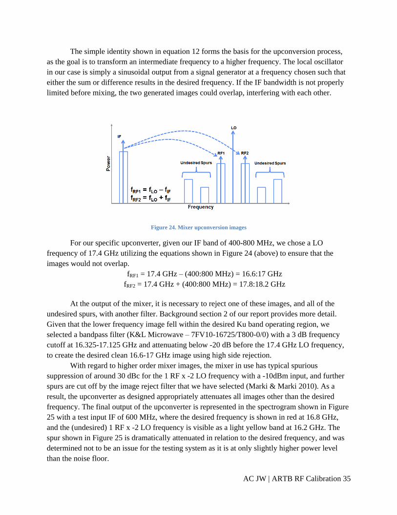
The simple identity shown in equation 12 forms the basis for the upconversion process,
as the goal is to transform an intermediate frequency to a higher frequency. The local oscillator
in our case is simply a sinusoidal output from a signal generator at a frequency chosen such that
either the sum or difference results in the desired frequency. If the IF bandwidth is not properly
limited before mixing, the two generated images could overlap, interfering with each other.
Figure 24. Mixer upconversion images
For our specific upconverter, given our IF band of 400-800 MHz, we chose a LO
frequency of 17.4 GHz utilizing the equations shown in Figure 24 (above) to ensure that the
images would not overlap.
fRF1 = 17.4 GHz – (400:800 MHz) = 16.6:17 GHz
fRF2 = 17.4 GHz + (400:800 MHz) = 17.8:18.2 GHz
At the output of the mixer, it is necessary to reject one of these images, and all of the
undesired spurs, with another filter. Background section 2 of our report provides more detail.
Given that the lower frequency image fell within the desired Ku band operating region, we
selected a bandpass filter (K&L Microwave – 7FV10-16725/T800-0/0) with a 3 dB frequency
cutoff at 16.325-17.125 GHz and attenuating below -20 dB before the 17.4 GHz LO frequency,
to create the desired clean 16.6-17 GHz image using high side rejection.
With regard to higher order mixer images, the mixer in use has typical spurious
suppression of around 30 dBc for the 1 RF x -2 LO frequency with a -10dBm input, and further
spurs are cut off by the image reject filter that we have selected (Marki & Marki 2010). As a
result, the upconverter as designed appropriately attenuates all images other than the desired
frequency. The final output of the upconverter is represented in the spectrogram shown in Figure
25 with a test input IF of 600 MHz, where the desired frequency is shown in red at 16.8 GHz,
and the (undesired) 1 RF x -2 LO frequency is visible as a light yellow band at 16.2 GHz. The
spur shown in Figure 25 is dramatically attenuated in relation to the desired frequency, and was
determined not to be an issue for the testing system as it is at only slightly higher power level
than the noise floor.

AC JW | ARTB RF Calibration 36
Figure 25. Upconverter Test Spectrogram
3.1.2.1 Calibration Hardware
The calibration hardware that made up the DUT consisted largely of the double-balanced
mixer used as a phase detector, power dividers, and a phase shifter for intentionally putting the
system out of calibration. Two horn antennas and a power receiver were utilized to provide an
additional feedback loop capturing the radiated antenna patterns in order to determine accuracy
of the calibration hardware as illustrated in Figure 26.
Figure 26. Calibration hardware in blue box with power dividers used to split transmitted signals, and sent to phase
detector and horn antennas

AC JW | ARTB RF Calibration 37
Two 15dBi Ku band horn antennas (ATM – 51-441-6) were used as the radiators for the
experiment; a receiver antenna was implemented to capture the power levels of the radiated
antenna patterns. The phase detector, the same double balanced mixer employed in the actual
ARBT calibration system (Marki M1-1020) was used such that the DUT could be appropriately
characterized. A Sage Laboratories 6805-2 analog phase shifter was used to intentionally put the
system out of calibration in order to measure accuracy of the calibration hardware. The power
dividers used in the ARTB split the signals immediately before the antennas to send to the phase
detector.
3.2 Verification of Test System
Throughout the design of our project we went through two stages of verification to ensure
that our system was achieving sufficient functionality before testing. The first stage of
verification was during our FPGA design period; we wanted to make sure that each module
actually achieved its functionality when added to the most recent design. The second stage of
verification occurred while we built our upconverter. Given that the calibration hardware was our
DUT, we did not spend time verifying it outside of the actual test.
3.2.1 FPGA Design Verification
Given that the FPGA functionally stored, filtered and sent waveforms, there were
multiple modules that made up the entire FPGA design. We utilized MATLAB to test each block
of the FPGA design by generating sinusoidal waveforms in MATLAB that were scaled to 16-bit
signed integers, for a 2.8Gsps sampling rate, varying in frequency (range of 400-800 MHz in
intervals of 50 MHz) and duration. By using a universal asynchronous receiver/transmitter
(UART) cable to communicate between MATLAB and the FPGA, we were able to evaluate each
major checkpoint by sending a sinusoidal waveform from MATLAB to the FPGA and
sequentially receiving the stored or filtered waveform in MATLAB. Given that the waveform
data were scaled to 16-bit signed integers, we used big endian storage on both the MATLAB and
FPGA side allowing for plotting the transmitted and stored or filtered waveforms. In order to test
the sending waveforms over the DAC, we used an oscilloscope to examine the output analog
waveforms.
3.2.2 Upconverter Verification
Similar to the testing of our FPGA design, during our design of the upconverter, we ran
multiple tests beginning with each individual component of the full upconverter. Initially, given
that we were not ordering components but rather gathering components at our disposal, we used
a Network Analyzer to visualize the response of different components. After finding components
(lowpass filter, mixer, bandpass filter, and amplifier) that theoretically fit our upconversion need,
we ran simulations in Genesys5 to ensure that the upconverter would work. After running
simulations in Genesys, we built the upconverter and used a spectrum analyzer to observe the
converted signals ensuring that the upconverter was bringing the IF band signal (400-800 MHz)
5 Genesys is an RF design program.

AC JW | ARTB RF Calibration 38
up to Ku band with low jitter and high attenuation of unwanted spurs as desired. As we did with
each block of the FPGA design, we added the upconverter to the most recent FPGA design,
generated and sent a sine wave from MATLAB through the system and observed the spectrum
analyzer to ensure that the full FPGA and upconverter system were working together, as
illustrated in Figure 27.
Figure 27. Spectrogram (top) and trace (bottom) of 600 MHz sine wave converted up to 16.8 GHz, shown at peak of trace.
3.3 Measurement Techniques
We utilized a Picoscope controlled by MATLAB to measure and record output data. The
two sources of feedback measurement data for the experiment were the phase detector
measurements from the calibration module’s phase detector output, as well as the receive power
scans taken at a distance of 2 meters from the transmission antennas. The master channel diode
detector output was sent to a third channel on the Picoscope; the diode detector output was an
envelope of the transmitted signal acting as a trigger. The Picoscope measurement setup is
depicted in Figure 28.

AC JW | ARTB RF Calibration 39
Figure 28. Picoscope three channel measurement setup
There were three main measurement techniques. The phase detector relied on very
specific calibration waveforms in order to calculate the transmit signal phase offset between the
two channels. The received power measurement scanned a purposely induced interferometer
pattern, described in detail later in this section. Lastly, MATLAB was used to control all
measurements on the Picoscope.
3.3.1 Calibration Waveforms
The phase detector had the ability to detect transmit signal phase offsets with specific
calibration waveforms. The calibration waveforms were essentially five 1µs chips, that varied
slightly between the master (reference) channel and slave (test) channel as illustrated in Figure
29.

AC JW | ARTB RF Calibration 40
Figure 29. Calibration waveform theory
For the untouched “reference” channel, we sent a normal 5µs 700 MHz sine wave with no phase
offset. For the “test” channel, we sent five distinct 1µs chips. The first “sync” chip was a 702
MHz sine wave with no phase offset; the next 4µs chips were a 700 MHz 90° phase stepped sine
wave. The two MHz difference between the sync chips would act as a trigger on the Picoscope
by resulting in a low frequency sine wave. The next 4µs chips would result in four DC voltages,
from which we determined the transmit signal phase offset between the two channels using
equation 13.
ɸ = 𝑡𝑎𝑛−1(𝑉4− 𝑉2
𝑉1− 𝑉3) (13)
3.3.2 Interferometer Broadside Null
The main reason for measuring the received power was to track the beam angle of the
antenna pattern; the feedback of the antenna pattern gave us the ability to determine whether the
system was in-phase. Relying solely on the calibration module without prior characterization, the
phase detector output did not accurately reflect the true offset of the system. We determined that
the easiest way to track the beam angle would be to induce an interferometer; an interferometer
occurs when two signals are 180° out of phase in relationship to each other. The destructive
interference between their antenna patterns results in a deep power null at the center of the beam
pattern, referred to as a broadside null. Figure 30 demonstrates the fact that simulating an
interferometer using the out-of-phase power data was easier and more accurate than using the in-
phase data. For the in-phase data, the slope of the power measurement was very low, and as such
accuracy of deriving the beam angle was correspondingly low, but with the out-of-phase data,
the slope was much more dramatic, making it easy to derive the beam angle with high accuracy.
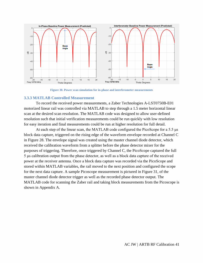
AC JW | ARTB RF Calibration 41
Figure 30. Power scan simulation for in-phase and interferometer measurements
3.3.3 MATLAB Controlled Measurement
To record the received power measurements, a Zaber Technologies A-LST0750B-E01
motorized linear rail was controlled via MATLAB to step through a 1.5 meter horizontal linear
scan at the desired scan resolution. The MATLAB code was designed to allow user-defined
resolution such that initial verification measurements could be run quickly with low resolution
for easy iteration and final measurements could be run at higher resolution for full detail.
At each step of the linear scan, the MATLAB code configured the PicoScope for a 5.5 μs
block data capture, triggered on the rising edge of the waveform envelope recorded at Channel C
in Figure 28. The envelope signal was created using the master channel diode detector, which
received the calibration waveform from a splitter before the phase detector mixer for the
purposes of triggering. Therefore, once triggered by Channel C, the PicoScope captured the full
5 μs calibration output from the phase detector, as well as a block data capture of the received
power at the receiver antenna. Once a block data capture was recorded via the PicoScope and
stored within MATLAB variables, the rail moved to the next position and configured the scope
for the next data capture. A sample Picoscope measurement is pictured in Figure 31, of the
master channel diode detector trigger as well as the recorded phase detector output. The
MATLAB code for scanning the Zaber rail and taking block measurements from the Picoscope is
shown in Appendix A.
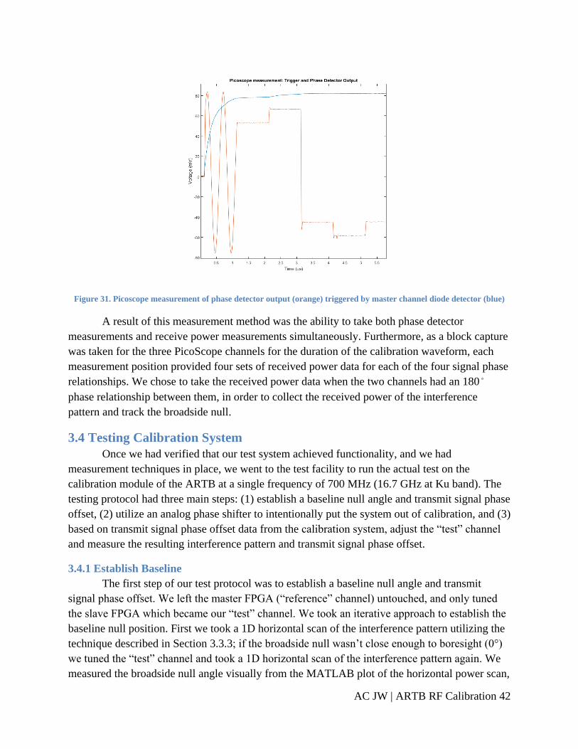
AC JW | ARTB RF Calibration 42
Figure 31. Picoscope measurement of phase detector output (orange) triggered by master channel diode detector (blue)
A result of this measurement method was the ability to take both phase detector
measurements and receive power measurements simultaneously. Furthermore, as a block capture
was taken for the three PicoScope channels for the duration of the calibration waveform, each
measurement position provided four sets of received power data for each of the four signal phase
relationships. We chose to take the received power data when the two channels had an 180˚
phase relationship between them, in order to collect the received power of the interference
pattern and track the broadside null.
3.4 Testing Calibration System
Once we had verified that our test system achieved functionality, and we had
measurement techniques in place, we went to the test facility to run the actual test on the
calibration module of the ARTB at a single frequency of 700 MHz (16.7 GHz at Ku band). The
testing protocol had three main steps: (1) establish a baseline null angle and transmit signal phase
offset, (2) utilize an analog phase shifter to intentionally put the system out of calibration, and (3)
based on transmit signal phase offset data from the calibration system, adjust the “test” channel
and measure the resulting interference pattern and transmit signal phase offset.
3.4.1 Establish Baseline
The first step of our test protocol was to establish a baseline null angle and transmit
signal phase offset. We left the master FPGA (“reference” channel) untouched, and only tuned
the slave FPGA which became our “test” channel. We took an iterative approach to establish the
baseline null position. First we took a 1D horizontal scan of the interference pattern utilizing the
technique described in Section 3.3.3; if the broadside null wasn’t close enough to boresight (0°)
we tuned the “test” channel and took a 1D horizontal scan of the interference pattern again. We
measured the broadside null angle visually from the MATLAB plot of the horizontal power scan,
AC JW | ARTB RF Calibration 43
finding the lowest power level and recording its respective angle. Once the broadside null was
within a few degrees of boresight and we had established our baseline null angle, we investigated
consistency of the calibration module. In order to investigate consistency, we sent the calibration
waveforms described in Section 3.3.2 and recorded the phase detector output of the calibration
module over five full system resets (power off and on all power supplies to amplifiers, VC707
boards, etc.) with 1000 measurements; MATLAB calculated the transmit signal phase offset
using equation 13, based on the average of each DC voltage.
3.4.2 Investigate Accuracy of Calibration Module
Once we had established a baseline null position and transmit signal phase offset, we
wanted to investigate the accuracy of the calibration module. We first applied an intentional
phase shift to the “test” channel that put the system out of calibration. Next, we recorded the
interference pattern and calibration phase detector output; we only recorded the interference
pattern to ensure that the baseline null position had shifted. We then recalibrated the system
based solely on the calibration phase detector output and lastly, recorded the resulting
interference pattern and calibration phase detector output. The figure of merit was the accuracy
between the baseline null angle and the recalibrated null angle. We applied 10 different phase
shifts between -180 to 180° with an analog phase shifter, recording the initial and resulting null
angle and transmit signal phase offset for each phase shift.
3.5 Analysis
The final objective of this project was to make sense of all the data we had collected,
drawing insight into the behavior of the calibration system. The data collected fell into two
categories, broadside null angle in terms of off broadside angle (°) and calculated transmit signal
phase offset (°). In order to analyze the consistency aspect of the calibration module, we
calculated the mean and range of the calculated transmit signal phase offsets from Section 4.4.1.
We utilized MATLAB to generate histograms highlighting the consistency of the phase detected
offsets; we generated scatter plots comparing the initial and resulting null angle and calculated
transmit signal phase offset to analyze the accuracy of the calibration module.

AC JW | ARTB RF Calibration 44
4. Results The test system designed during this project required verification prior to data collection.
Preliminary verification tests were run for the FPGA design, upconverter hardware and
antenna/receiver feedback loop. Once the test system was determined to be operational, we
conducted our experiment. The data collected consisted of 1D horizontal scans of received power
from the two horn antennas as well as phase detector voltage output over time; all of the data
were collected by a PicoScope which was controlled by MATLAB, making it easy to analyze
directly from MATLAB. Figure 32 shows pictures of the entire test setup from waveform
generation to our horn antennas and receiver antenna feedback loop.
Figure 32. Waveform generation and transmission (left) with laptop, two VC707 board and RF upconverter and
calibration hardware in black chassis and feedback loop (right) with Zaber Motorized Rail, two horn antennas and
receiver antenna
4.1 Verification Results
Prior to collecting data, we had to verify that our test system was functioning as desired.
The first step was ensuring that the FIR filtering in our FPGA design was outputting filtered
waveforms as expected. In order to simulate the FIR, MATLAB generated a 4 µs sine wave and
sent it to the FPGA. The data were then stored in an off-chip DDR send-buffer memory location
and sent to the FIR by the DMA. The FIR outputted data were received by the DMA and stored
in an off-chip DDR receive-buffer memory location. The FPGA then sent the receive-buffer data
back to MATLAB. Figure 33 demonstrates the working FIR filter for 1
3 sample delay and
advance as well as a baseline wave with no delay or advance after inputting a 200 MHz sine
wave.

AC JW | ARTB RF Calibration 45
Figure 33. Single period of FIR filtered output for 1/3 sample delay, no delay or advance and 1/3 sample advance
The second step was ensuring that our upconverter design was converting our 400-800
MHz IF band up to 16.6-17 GHz Ku band successfully. We used a Keysight Technologies
N9344C Handheld Spectrum Analyzer to run a spectrogram on the upconverter output in order to
ensure that it was attenuating spurs with low jitter as desired; Figure 34 highlights a spectrogram
of the functioning upconverter bringing 600 MHz up to 16.8 MHz.
Figure 34. Spectrogram at 17.4 GHz (LO) center frequency with desired 16.8 GHz RF frequency (red) and 16.2 GHz
second-order spur (yellow) highly attenuated
LO

AC JW | ARTB RF Calibration 46
The third step was ensuring synchronization between our two FPGAs given that the
eventual data collection relied heavily on phase alignment of outputted waveforms between the
two FPGAs. Using a Keysight MS09404-A High-Speed Oscilloscope, we captured and analyzed
the outputted waveforms of the two FPGAs. With a master FPGA triggering a slave FPGA, the
outputted waveforms would have some time offset between them purely from the amount of time
it took for the trigger to occur. However, our synchronization only required phase alignment
between the two channels because we were able to control when we sampled the phase detector
output and radiation patterns for data. Figure 35 gives an 18µs wideview of the synchronized
waveforms while Figure 36 gives a close view.
Figure 35. Oscilloscope wide view of synchronized FPGA outputs for 18µs waveform duration of master (green) and slave
(yellow) transmitted signals
Figure 36. Close view (1ns/div) of phase aligned synchronization within 1ns between master (green) and slave (yellow)
transmitted signals
The final step prior to beginning data collection was checking the environment of the
antenna/receiver feedback loop. While the idea of inducing an interferometer works in theory,
we needed to check that it was a possibility in our test environment, specifically verifying that
the antennas would create a distinctive and easily trackable broadside null. Using the receiver
antenna mounted on a Zaber Technologies A-LST0750B-E01 motorized linear rail, we took a 1D
horizontal scan of the received power; Figure 37 demonstrates the interferometer antenna pattern
in our test environment.
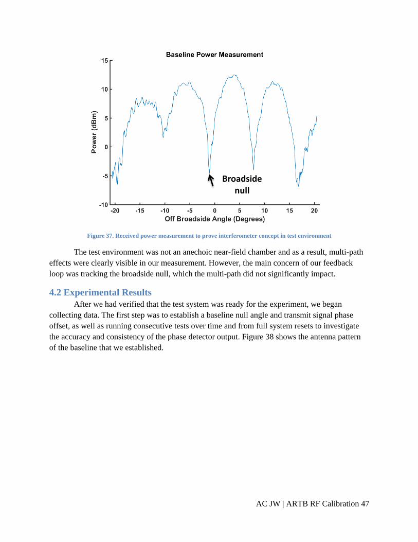
AC JW | ARTB RF Calibration 47
Figure 37. Received power measurement to prove interferometer concept in test environment
The test environment was not an anechoic near-field chamber and as a result, multi-path
effects were clearly visible in our measurement. However, the main concern of our feedback
loop was tracking the broadside null, which the multi-path did not significantly impact.
4.2 Experimental Results
After we had verified that the test system was ready for the experiment, we began
collecting data. The first step was to establish a baseline null angle and transmit signal phase
offset, as well as running consecutive tests over time and from full system resets to investigate
the accuracy and consistency of the phase detector output. Figure 38 shows the antenna pattern
of the baseline that we established.
Broadside null

AC JW | ARTB RF Calibration 48
Figure 38. Baseline antenna pattern with broadside null at -1.16° off broadside angle
While an ideal interferometer would produce a deep broadside null at 0° off broadside
angle, we tried to get our broadside null as close to 0° as possible. The fact that we did not get
exactly 0° was not significant, as we were simply establishing a baseline null position to refer to
when analyzing the consistency and accuracy of the DUT. Figure 39 shows the baseline phase
detector output over 1000 measurements, highlighting the consistency of the calibration module.
Figure 39. Baseline phase detector output over 1000 700 MHz calibration waveform measurements resulting in a
calculated phase offset of -51.683°
Broadside null

AC JW | ARTB RF Calibration 49
We ran 1000 measurements over 5 full system resets and got very similar phase detector
output and baseline power measurement. While there is some noise in Figure 39 at each DC
voltage, the noise was not significant in the transmit signal phase offset calculation as each
voltage level was averaged prior to the calculation. Figure 40 depicts a histogram of the actual
baseline transmit signal phase offset calculations and their consistency.
Figure 40. Baseline calculated transmit signal phase offset consistent within ~1° over 1000 measurements
As shown in Figure 40, the phase detector output is consistent within <1° over 1000
measurements from full system reset. Having established consistency of the calibration output as
well as a baseline null angle and transmit signal phase offset, our next step was to apply external
phase offsets using an analog phase shifter in order to investigate the accuracy of getting back to
our baseline null angle and transmit signal phase offset relying solely on the calibration data. The
accuracy is of concern as the ARTB will rely solely on the calibration data to guide the
transmission of waveforms back to full synchronization, without any additional radiation pattern
feedback loop. After applying an external phase offset, we first sent the calibration waveforms
and analyzed the phase detector output, as shown in Figure 41.
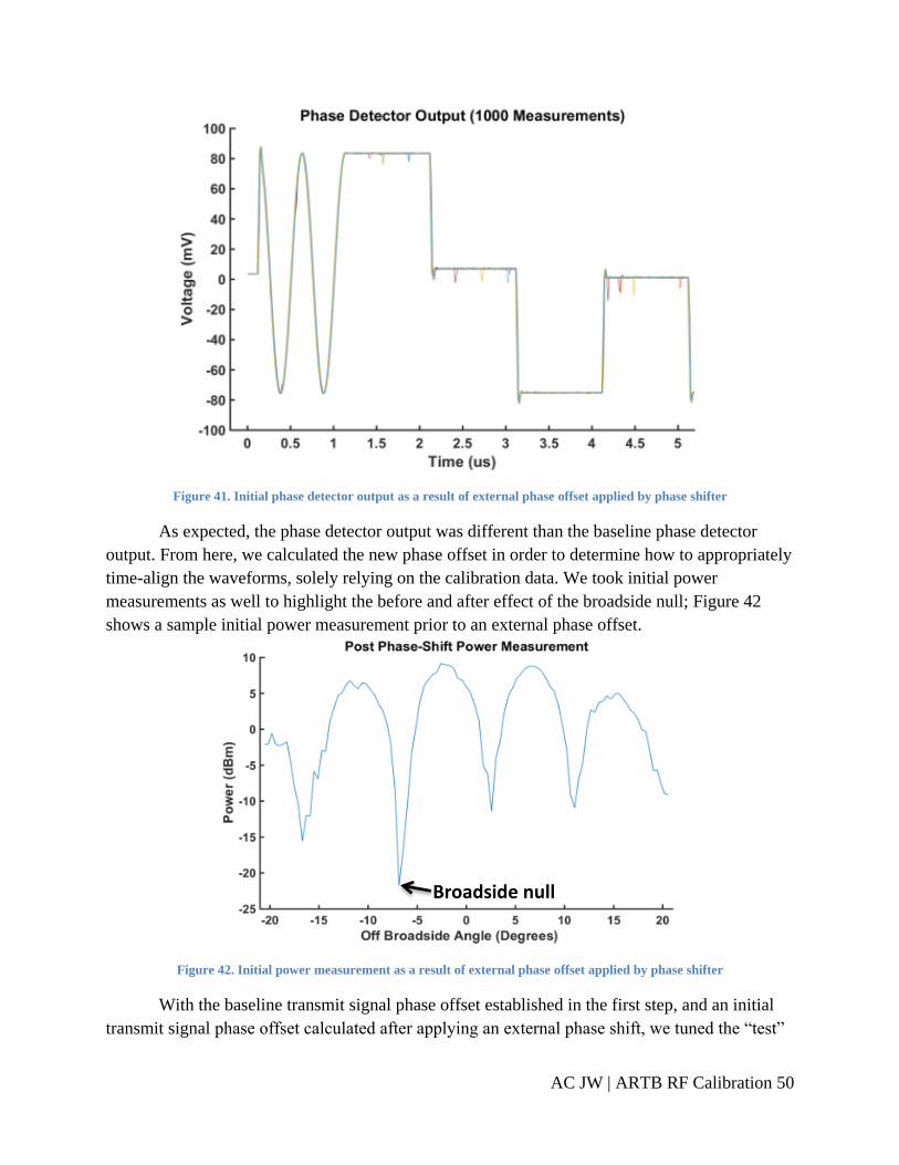
AC JW | ARTB RF Calibration 50
Figure 41. Initial phase detector output as a result of external phase offset applied by phase shifter
As expected, the phase detector output was different than the baseline phase detector
output. From here, we calculated the new phase offset in order to determine how to appropriately
time-align the waveforms, solely relying on the calibration data. We took initial power
measurements as well to highlight the before and after effect of the broadside null; Figure 42
shows a sample initial power measurement prior to an external phase offset.
Figure 42. Initial power measurement as a result of external phase offset applied by phase shifter
With the baseline transmit signal phase offset established in the first step, and an initial
transmit signal phase offset calculated after applying an external phase shift, we tuned the “test”
Broadside null
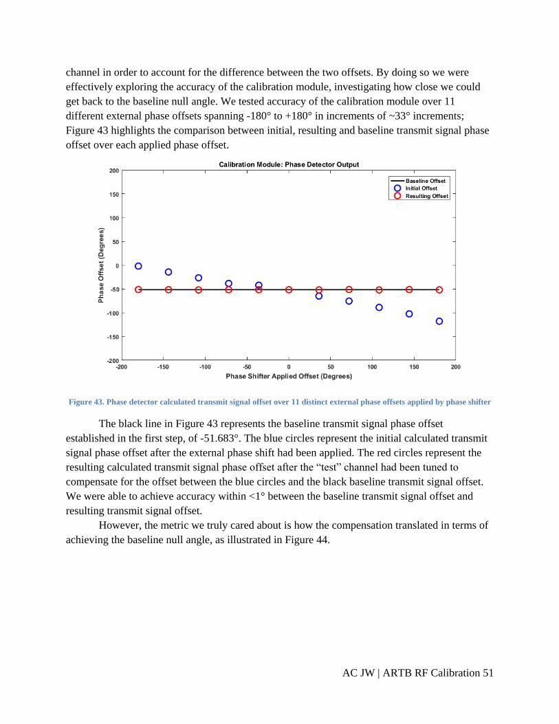
AC JW | ARTB RF Calibration 51
channel in order to account for the difference between the two offsets. By doing so we were
effectively exploring the accuracy of the calibration module, investigating how close we could
get back to the baseline null angle. We tested accuracy of the calibration module over 11
different external phase offsets spanning -180° to +180° in increments of ~33° increments;
Figure 43 highlights the comparison between initial, resulting and baseline transmit signal phase
offset over each applied phase offset.
Figure 43. Phase detector calculated transmit signal offset over 11 distinct external phase offsets applied by phase shifter
The black line in Figure 43 represents the baseline transmit signal phase offset
established in the first step, of -51.683°. The blue circles represent the initial calculated transmit
signal phase offset after the external phase shift had been applied. The red circles represent the
resulting calculated transmit signal phase offset after the “test” channel had been tuned to
compensate for the offset between the blue circles and the black baseline transmit signal offset.
We were able to achieve accuracy within <1° between the baseline transmit signal offset and
resulting transmit signal offset.
However, the metric we truly cared about is how the compensation translated in terms of
achieving the baseline null angle, as illustrated in Figure 44.

AC JW | ARTB RF Calibration 52
Figure 44. Comparison of initial null angle (blue) after applied phase shifter versus recalibrated null angle (red) based on
calibration phase offset data
Again, the black line in Figure 44 represents the baseline null angle established in the first step,
of -1.617° off broadside angle. The blue marks represent the initial broadside null angle,
recorded solely for comparison, after the external phase shift had been applied. The red marks
represent the resulting broadside null angle after the “test” channel had been tuned. Accuracy
within <1° in phase offset translated to accuracy within 0.15° in terms of off broadside angle.

AC JW | ARTB RF Calibration 53
5. Discussion The two sets of data collected in our test consisted of the calculated transmit signal phase
offsets from the calibration phase detector output, and the 1D horizontal power scans of the
radiated interference patterns. The first step in analyzing our data was to investigate the
implication of the results. The second step was to highlight possible areas of concern that may
have affected the results significantly.
5.1 Implication of Results
Given the measured data concerning the ability of the calibration system to account for
external phase offsets, it is possible to come to conclusions concerning whether the calibration
system appropriately meets the system requirements for ensuring that the beam pattern is
directed at the desired angle. The primary requirement for the system is that the calibration
between time-steered channels is not the limiting factor in the testbed’s beam steering ability.
The other components which are used to steer the beam are the phase shifters for each element
within the AESA panels. These phase shifters have 6 bit phase resolution, allowing for phase
resolution to 5.625˚. As the calibration system was able to correct for the phase difference
between the test and reference channels within 1˚, we do not believe that the calibration system
is the limiting factor of the system. One qualification to claiming that the calibration system is
not the limiting factor of the system is that the single frequency experiment does not predict the
correction consistency of achieving a wideband null over the full system bandwidth. Given the
frequency independence of the accuracy of phase measurements from the calibration module, we
do not expect testing over the full system bandwidth to dramatically alter the accuracy and
consistency of achieving a desired beam angle, but the calibration module would require
additional verification for complete assurance.
5.2 Possible Data Concerns
A few concerns arose while interpreting the data related to the testing setup and
environment. Two such considerations were the viability of performing a horizontal linear scan
as opposed to a curved scan, and the multipath effects of the testing room where the
measurements were taken. In this section we will investigate these concerns and show that their
effects do not negatively alter the results and conclusions of the experiment.
5.2.1 Horizontal Linear Scan
During the course of the project, the decision to use a horizontal linear scan for recording
the power measurements was brought up as a possible concern, as the distance between the
transmission and receiver antennas is larger at the edges of the scan. As depicted in Figure 45,
given the full scan angle and the distance of 2 meters between the transmission and receiver
antennas, the largest extent of this difference in distance was calculated to be 136 mm at the scan
edge.

AC JW | ARTB RF Calibration 54
Figure 45. Horizontal Linear Scan Measurement Distance vs. Curved Scan
Two alternatives to the chosen scan method would have been possible to counteract this
difference in distance. A curved scan as depicted in Figure 45 would allow the receiver antenna
to maintain a constant 2 meter distance from the transmission antennas, but would also require
hardware to perform a curved scan, or manual positioning of the receiver. The other alternative
would be to rotate the tripod head which held the transmission antenna setup while keeping the
receiver antenna in a constant position. This method would have also required manual rotation to
take each successive measurement. Both of these would dramatically increase the measurement
time and reduce the accuracy of measurement location, adding in the potential for operator error.
As such, the horizontal scan remained the most attractive measurement for the test.
The decision to perform the test with the linear scan required analysis of the system
geometry to ensure that the difference in distance at the edges of the scan did not negatively
affect the resultant data. At the worst case, the distance differential was calculated to be 136 mm.
Given the 16.7 GHz test frequency that was employed, the wavelength (calculated to be 17.964
mm) was determined to be sufficiently small for a significant phase difference between the ideal
curved measurement and the linear scan measurement; 7.57 wavelengths of the transmitted tone
would occur between the two. Therefore, the difference in distance would dramatically affect
any phase measurements taken. For the purposes of aligning the null power positions however,
the phase of the signal at the receiver is not important.
The other possible implication of the difference in distance between the center and edges
of the measurement scan is the free space power loss. Given the Friis Equation represented in
equation 14, it is possible to determine the power loss over the 136 mm distance in relation to the
power at the center of the scan.
𝑷𝒓 = 𝑷𝒕 + 𝑮𝒕 + 𝑮𝒓 + 𝟐𝟎𝒍𝒐𝒈 (𝝀
𝟒𝝅∆𝒓) (14)
In equation 14, Pt = transmitted power, Gt = transmitter gain, Gr = receiver gain, Δr =
distance between the antennas, λ = 2π/f where f = frequency, and Pr = received power. As the

AC JW | ARTB RF Calibration 55
136 mm distance is very small, the power loss was calculated to be 0.1 dB. The 0.1 dB loss was
determined not to be substantial for the power measurement especially because we were only
measuring the broadside null angle. As such the horizontal linear scan was deemed accurate for
the conclusions reached through this experiment.
5.2.2 Multipath effects
One other concern which arose throughout the experiment involved the multipath effects
of the testing environment. It was evident early within the testing period that the physical
geometry and layout of the testing room induced reflection effects which interfered with the
signal measurement at the receiver antenna. The multipath interference is reflected in Figure 46
which shows the results of all the final null location measurements from the return-to-baseline
tests.
Figure 46. Overlaid return-to-baseline power scan measurements
The multipath effects are most notable on the edges of the scan region, where there is
more interference from the walls of the testing environment and other objects within the room.
Fortunately, the effects of the multipath interference were consistent throughout the testing
period, as the room layout was not changed between tests. The consistency of the effects is
represented in Figure 46; the return-to-baseline test measurements were taken at different times
throughout the testing period, and the interference pattern was observed to be the same over all
of the tests. Furthermore, the multipath effects did not inhibit our ability to identify the location
of the broadside null from the power measurement or use the phase data gathered from the
calibration module to re-align the null at the baseline position. It was therefore determined that
although it would be beneficial to carry out additional testing in an anechoic chamber in the
future, the testing environment was appropriate for the experiment outlined in this report.
Broadside null

AC JW | ARTB RF Calibration 56
6. Conclusions
6.1 Measurement Conclusions
Through analysis of the gathered results and the testing system, it was determined that the
ARTB calibration system was able to accurately and consistency provide phase difference data
to account for an external offset and align the beam pattern with the desired baseline. This
conclusion was reached as the ability to use the ARTB calibration system to account for external
offset was determined not to be the limiting factor of the beam steering capabilities of the
Airborne Radar Testbed antenna system.
6.2 Future Steps
Given an extended testing period, it would be beneficial to gather additional data to more
fully characterize the behavior of the Airborne Radar Testbed’s calibration system. The first
additional experiment would be to perform the same test as described in this report within an
anechoic chamber, something which was not possible during this project due to scheduling and
timing constraints with the near-field chamber at Lincoln Laboratory. Testing in an anechoic
chamber would eliminate the multipath behavior observed in the measured power scan data and
provide addition assurance that the multipath interference did not negatively affect the results of
the experiment.
Beyond carrying out the same test in an anechoic chamber, it would also be beneficial to
test at wider bandwidths. The test at a single frequency of 16.7 GHz (700 MHz IF) provided an
understanding of the accuracy and consistency of the phase measurement performed by the
calibration system and the ability to use this measurement to return to a baseline beam angle, but
for a single frequency, phase and time-delay are essentially the same, as the frequency
dependence of phase shift is constant for a single frequency. As a result, using the phase detector
measurement to re-align the baseline null angle at a single frequency does not mean that the null
angle is properly aligned for the other frequencies within the transmission band. Testing at wider
bandwidths, the transmit signal phase offset measurements would be taken in the same way as
they were for a single frequency: by sending frequency specific calibration waveforms and
measuring the transmit signal phase offset between the two channels.
The foundation for the full bandwidth experiment is already developed through the FPGA
design that was created for the experiment described within this report. The FIR filters developed
support both sub-sample time delay control as well as continuous phase control, allowing for the
necessary corrections to re-align a wideband null to a recorded baseline.
Along with the wider bandwidth test, full characterization of the calibration system
would require an understanding of the effects of the environmental conditions on the system’s
ability to properly calibrate the antenna array system. As the system will eventually be employed
on a Twin Otter aircraft, it will be subject to temperature variation as well as vibration
throughout a flight. Understanding the implications of these environmental conditions would
allow for conclusions to be reached regarding how often the system would need to be calibrated

AC JW | ARTB RF Calibration 57
using the calibration system, or if a single calibration before flight to account for startup offsets
would be sufficient.

AC JW | ARTB RF Calibration 58
Works Cited
Coleman, C. (2004). An Introduction to Radio Frequency Engineering (86-108). Cambridge,
United Kingdom: Cambridge University Press. Print.
Davis, A. & Agarwal, K. (2001) Radio Frequency Circuit Design (271-274). New York, NY:
John Wiley & Sons, Inc. Print.
Longbrake, M. (2012). True Time-Delay Beamsteering for Radar. IEEE National Aerospace and
Electronics Conference (NAECON), 25–27 July, 246–249. Retrieved from
http://ieeexplore.ieee.org/document/6531062/
Marvasti, F. A., ed. (2001). Nonuniform sampling: Theory and practice (842-852). New York,
NY: Kluwer Academic/Plenum Publ. Print.
Poornachandra, S. & Sasikala B. (2010). Design of FIR Filter - Windowing Techniques. In
Digital Signal Processing (FIR-32-FIR-49), 3rd Edition. West Patel Nagar, New Delhi:
Tata McGraw Hill Education Private Limited. Print.
Prabhu, K. M. (2014). Truncated Taylor Family. In Window Functions and Their Applications in
Signal Processing (94-95). Boca Raton, FL: CRC Press. Print.
Shannon, C. (1998). Communication in the Presence of Noise. Proceedings of the IEEE, 86(2),
447-457. (Reprinted from Proceedings of the IRE, 37, 10-21)
Skolnik, M. (2008). Radar Handbook, 3rd Edition (1.1 – 13.7). The McGraw-Hill Companies,
USA. Print.
Välimäki, V. (1995). Discrete-Time Modeling of Acoustic Tubes Using Fractional Delay Filters.
Ph.D. dissertation, Helsinki University of Technology, Helsinki, Finland. Retrieved from
http://users.spa.aalto.fi/vpv/publications/vesan_vaitos/abstract.pdf
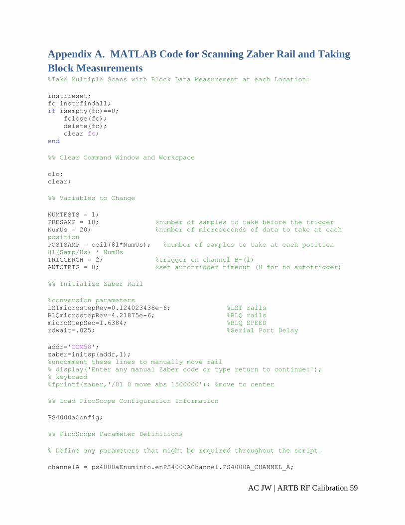
AC JW | ARTB RF Calibration 59
Appendix A. MATLAB Code for Scanning Zaber Rail and Taking
Block Measurements %Take Multiple Scans with Block Data Measurement at each Location:
instrreset; fc=instrfindall; if isempty(fc)==0; fclose(fc); delete(fc); clear fc; end
%% Clear Command Window and Workspace
clc; clear;
%% Variables to Change
NUMTESTS = 1; PRESAMP = 10; %number of samples to take before the trigger NumUs = 20; %number of microseconds of data to take at each
position POSTSAMP = ceil(81*NumUs); %number of samples to take at each position
81(Samp/Us) * NumUs TRIGGERCH = 2; %trigger on channel B-(1) AUTOTRIG = 0; %set autotrigger timeout (0 for no autotrigger)
%% Initialize Zaber Rail
%conversion parameters LSTmicrostepRev=0.124023438e-6; %LST rails BLQmicrostepRev=4.21875e-6; %BLQ rails microStepSec=1.6384; %BLQ SPEED rdwait=.025; %Serial Port Delay
addr='COM58'; zaber=initsp(addr,1); %uncomment these lines to manually move rail % display('Enter any manual Zaber code or type return to continue:'); % keyboard %fprintf(zaber,'/01 0 move abs 1500000'); %move to center
%% Load PicoScope Configuration Information
PS4000aConfig;
%% PicoScope Parameter Definitions
% Define any parameters that might be required throughout the script.
channelA = ps4000aEnuminfo.enPS4000AChannel.PS4000A_CHANNEL_A;

AC JW | ARTB RF Calibration 60
channelB = ps4000aEnuminfo.enPS4000AChannel.PS4000A_CHANNEL_B; channelC = ps4000aEnuminfo.enPS4000AChannel.PS4000A_CHANNEL_C; channelD = ps4000aEnuminfo.enPS4000AChannel.PS4000A_CHANNEL_D;
%% PicoScope Connection
% Create device - specify serial number if required % Specify serial number as 2nd argument if required. ps4000aDeviceObj = icdevice('picotech_ps4000a_generic', '');
% Connect device connect(ps4000aDeviceObj);
%% Display PicoScope Unit Information
[infoStatus, unitInfo] = invoke(ps4000aDeviceObj, 'getUnitInfo');
disp(unitInfo);
%% Set PicoScope Channels
% Default driver settings applied to channels are listed below - % use ps4000aSetChannel to turn channels on or off and set voltage ranges, % coupling, as well as analogue offset.
% In this example, data is only collected on Channel A so default settings % are used and channels B to H are switched off.
% Channels : 1 - 7 (ps4000aEnuminfo.enPS4000AChannel.PS4000A_CHANNEL_B
- PS4000A_CHANNEL_H) % Enabled : 0 % Type : 1 (ps4000aEnuminfo.enPS4000ACoupling.PS4000A_DC) % Range : 8 (ps4000aEnuminfo.enPS4000ARange.PS4000A_5V) % Analogue Offset: 0.0
% Execute device object function(s) [status.setChA] = invoke(ps4000aDeviceObj, 'ps4000aSetChannel', 0, 1, 1, 8,
0.0); %Power Reading [status.setChB] = invoke(ps4000aDeviceObj, 'ps4000aSetChannel', 1, 1, 1, 3,
0.0); %Master Diode Detector [status.setChC] = invoke(ps4000aDeviceObj, 'ps4000aSetChannel', 2, 1, 1, 3,
0.0); %Slave Diode Detector [status.setChD] = invoke(ps4000aDeviceObj, 'ps4000aSetChannel', 3, 1, 1, 3,
0.0); %Mixer Output
%if(ps4000aDeviceObj.channelCount == PicoConstants.QUAD_SCOPE ||
ps4000aDeviceObj.channelCount == PicoConstants.OCTO_SCOPE) % [status.setChC] = invoke(ps4000aDeviceObj, 'ps4000aSetChannel', 2, 0, 1,
8, 0.0); % [status.setChD] = invoke(ps4000aDeviceObj, 'ps4000aSetChannel', 3, 0, 1,
8, 0.0); %end

AC JW | ARTB RF Calibration 61
if(ps4000aDeviceObj.channelCount == PicoConstants.OCTO_SCOPE)
[status.setChE] = invoke(ps4000aDeviceObj, 'ps4000aSetChannel', 4, 0, 1,
8, 0.0); [status.setChF] = invoke(ps4000aDeviceObj, 'ps4000aSetChannel', 5, 0, 1,
8, 0.0); [status.setChG] = invoke(ps4000aDeviceObj, 'ps4000aSetChannel', 6, 0, 1,
8, 0.0); [status.setChH] = invoke(ps4000aDeviceObj, 'ps4000aSetChannel', 7, 0, 1,
8, 0.0);
end
% Obtain the maximum ADC Count from the driver maxADCCount = double(get(ps4000aDeviceObj, 'maxADCValue'));
%% Verify Timebase Index and Maximum Number of Samples
% Driver default timebase index used - use ps4000aGetTimebase2 to query the % driver as to suitability of using a particular timebase index and the % maximum number of samples available in the segment selected (the buffer % memory has not been segmented in this example) then set the 'timebase' % property if required. % % To use the fastest sampling interval possible, set one analogue channel % and turn off all other channels. % % Use a while loop to query the function until the status indicates that a % valid timebase index has been selected. In this example, the timebase % index of 79 is valid.
% Initial call to ps4000aGetTimebase2 with parameters: % timebase : 0 % segment index : 0
status.getTimebase2 = PicoStatus.PICO_INVALID_TIMEBASE; timebaseIndex = 0; while(status.getTimebase2 == PicoStatus.PICO_INVALID_TIMEBASE)
[status.getTimebase2, timeIntervalNanoSeconds, maxSamples] =
invoke(ps4000aDeviceObj, 'ps4000aGetTimebase2', timebaseIndex, 0);
if(status.getTimebase2 == PicoStatus.PICO_OK) break; else timebaseIndex = timebaseIndex + 1; end
end
set(ps4000aDeviceObj, 'timebase', timebaseIndex);
%% Set Simple Trigger % Set a trigger on Channel A, with an auto timeout - the default value for

AC JW | ARTB RF Calibration 62
% delay is used.
% Trigger properties and functions are located in the Instrument % Driver's Trigger group.
triggerGroupObj = get(ps4000aDeviceObj, 'Trigger'); triggerGroupObj = triggerGroupObj(1);
% Set the autoTriggerMs property in order to automatically trigger the % oscilloscope after 1 second if a trigger event has not occurred. Set to 0 % to wait indefinitely for a trigger event.
set(triggerGroupObj, 'autoTriggerMs', AUTOTRIG);
% Channel : 0 (ps4000aEnuminfo.enPS4000AChannel.PS4000A_CHANNEL_A) % CHANGE THIS TO TRIGGER ON THE ENVELOPE CHANNEL % Threshold : 10 (mV) % Direction : 2
(ps4000aEnuminfo.enPS4000AThresholdDirection.PS4000A_RISING)
[status.setSimpleTrigger] = invoke(triggerGroupObj, 'setSimpleTrigger',
TRIGGERCH, 5, 2);
%% Set PicoScope Block Parameters
% Capture a block of data and retrieve data values for Channel A.
% Block data acquisition properties and functions are located in the % Instrument Driver's Block group.
blockGroupObj = get(ps4000aDeviceObj, 'Block'); blockGroupObj = blockGroupObj(1);
% Set pre-trigger and post-trigger samples as required % 10 presamples and POSTSAMP postsamples
set(ps4000aDeviceObj, 'numPreTriggerSamples', PRESAMP); set(ps4000aDeviceObj, 'numPostTriggerSamples', POSTSAMP);
%% Scan and Measure
%comparizon values used for direction selection left = 'left'; right = 'right'; initdir = right;
%prompt the user to select initial direction %initdir = input('Choose a direction (left or right): ');
%initialization settings for step size and maximum X value XMaxVal = 3000000;
%User selection of the stepsize
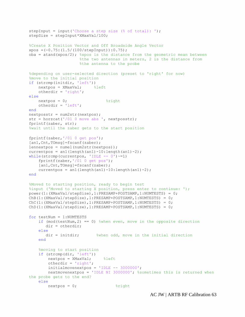
AC JW | ARTB RF Calibration 63
stepInput = input('Choose a step size (% of total): '); stepSize = stepInput*XMaxVal/100;
%Create X Position Vector and Off Broadside Angle Vector xpos =(-0.75:(1.5/(100/stepInput)):0.75); oba = atand(xpos/2); %xpos is the distance from the geometric mean between %the two antennas in meters, 2 is the distance from %the antenna to the probe
%depending on user-selected direction (preset to 'right' for now) %move to the initial position if (strcmp(initdir, 'left')) nextpos = XMaxVal; %left otherdir = 'right'; else nextpos = 0; %right otherdir = 'left'; end nextposstr = num2str(nextpos); str = horzcat('/01 0 move abs ', nextposstr); fprintf(zaber, str); %wait until the zaber gets to the start position
fprintf(zaber,'/01 0 get pos'); [an1,Cnt,TOmsg]=fscanf(zaber); lennextpos = numel(num2str(nextpos)); currentpos = an1(length(an1)-10:length(an1)-2); while(strcmp(currentpos, 'IDLE -- 0')~=1) fprintf(zaber,'/01 0 get pos'); [an1,Cnt,TOmsg]=fscanf(zaber); currentpos = an1(length(an1)-10:length(an1)-2); end
%Moved to starting position, ready to begin test %input ('Moved to starting X position, press enter to continue: '); power(1:(XMaxVal/stepSize),1:PRESAMP+POSTSAMP,1:NUMTESTS) = 0; ChB(1:(XMaxVal/stepSize),1:PRESAMP+POSTSAMP,1:NUMTESTS) = 0; ChC(1:(XMaxVal/stepSize),1:PRESAMP+POSTSAMP,1:NUMTESTS) = 0; ChD(1:(XMaxVal/stepSize),1:PRESAMP+POSTSAMP,1:NUMTESTS) = 0;
for testNum = 1:NUMTESTS if (mod(testNum,2) == 0) %when even, move in the opposite direction dir = otherdir; else dir = initdir; %when odd, move in the initial direction end
%moving to start position if (strcmp(dir, 'left')) nextpos = XMaxVal; %left otherdir = 'right'; initialmovenextpos = 'IDLE -- 3000000'; nextmovenextpos = 'IDLE NI 3000000'; %sometimes this is returned when
the probe gets to the end? else nextpos = 0; %right

AC JW | ARTB RF Calibration 64
otherdir = 'left'; initialmovenextpos = 'IDLE -- 0'; nextmovenextpos = 'IDLE NI 0'; %sometimes this is returned when the
probe gets to the end? end nextposstr = num2str(nextpos); str = horzcat('/01 0 move abs ', nextposstr); fprintf(zaber, str); %wait until the zaber gets to the start position
fprintf(zaber,'/01 0 get pos'); [an1,Cnt,TOmsg]=fscanf(zaber); currentpos = an1(length(an1)-numel(initialmovenextpos)-1:length(an1)-2);
while(strcmp(currentpos, initialmovenextpos) ~= 1 && strcmp(currentpos,
nextmovenextpos) ~= 1) fprintf(zaber,'/01 0 get pos'); [an1,Cnt,TOmsg]=fscanf(zaber); currentpos = an1(length(an1)-numel(initialmovenextpos)-1:length(an1)-
2); end
%Moved to starting position, ready to begin test (uncomment next line to %have system wait for user input on every scan) %input ('Moved to starting X position, press enter to continue: '); %probe is in initial position, read first power level from picoscope [status.runBlock] = invoke(blockGroupObj, 'runBlock', 0); [POSTSAMPles, overflow,
power(1,1:PRESAMP+POSTSAMP,testNum),ChB(1,1:PRESAMP+POSTSAMP,testNum),ChC(1,1
:PRESAMP+POSTSAMP,testNum),ChD(1,1:PRESAMP+POSTSAMP,testNum)] =
invoke(blockGroupObj, 'getBlockData', 0, 0, 1, 0);
for i = 1:(XMaxVal/stepSize) if (strcmp(dir, 'left')) nextpos = XMaxVal-(stepSize*i); %left else nextpos = stepSize*i; %right end nextposstr = num2str(nextpos); str = horzcat('/01 0 move abs ', nextposstr); fprintf(zaber, str);
%check if it has gotten there yet, wait until it gets there
fprintf(zaber,'/01 0 get pos'); [an1,Cnt,TOmsg]=fscanf(zaber); lennextpos = numel(num2str(nextpos)); currentpos = str2double(an1(length(an1)-lennextpos-1:length(an1)-1));
while(currentpos ~= nextpos)
fprintf(zaber,'/01 0 get pos'); [an1,Cnt,TOmsg]=fscanf(zaber); currentpos = str2double(an1(length(an1)-lennextpos-1:length(an1)-
1));

AC JW | ARTB RF Calibration 65
end %probe is in position, read power from picoscope [status.runBlock] = invoke(blockGroupObj, 'runBlock', 0); [POSTSAMPles, overflow,
power(i+1,1:PRESAMP+POSTSAMP,testNum),ChB(i+1,1:PRESAMP+POSTSAMP,testNum),ChC
(i+1,1:PRESAMP+POSTSAMP,testNum),ChD(i+1,1:PRESAMP+POSTSAMP,testNum)] =
invoke(blockGroupObj, 'getBlockData', 0, 0, 1, 0); end
powerdBm = (log(power/110.1)/0.1211); %%these values result from the
curvefit of the mV to dBm plot for i = 1:numel(powerdBm) if(powerdBm(i) == -Inf) powerdBm(i) = 0; end end end
%flip every even numbered test (as the test is taken left to right, the %data is reversed (may also need to take negative of nullAngle) for i = 1:NUMTESTS if (mod(i, 2) == 0) %even powerdBm(i,:) = fliplr(powerdBm(i,:)); end end
%% Disconnect Devices
% Disconnect device object from hardware. disconnect(ps4000aDeviceObj); delete(ps4000aDeviceObj); instrreset; fc=instrfindall; if isempty(fc)==0; fclose(fc); delete(fc); clear fc; end
%% Plot Gathered Data
timeNs = double(timeIntervalNanoSeconds) * double(0:PRESAMP+POSTSAMP - 1); timeUs = timeNs / 1e3;
%%plot power vs x-position %plot(xpos, power) %title('Received Power - Horizontal Slice'); %xlabel('Position (m)'); %ylabel('Voltage (mV)');
%%curve fitting %figure %plot(xpos, powerdBm) %title('Received Power - Horizontal Slice'); %xlabel('Position (m)');

AC JW | ARTB RF Calibration 66
%ylabel('Power (dBm)');
%figure %plot(oba, powerdBm) %xlim([-21 21]) %title('Received Power - Horizontal Slice'); %xlabel('Off Broadside Angle (Degrees)'); %ylabel('Power (dBm)');
%% Pull 1d Power Scan from Block Data sizedata = size(powerdBm); scandata(1:sizedata(1)) = 0; for i = 1:sizedata(1) scandata(i) = mean(powerdBm(i,800:1400)); end
figure(2) plot(oba, scandata) xlim([-21 21]) title('Received Power - Horizontal Slice'); xlabel('Off Broadside Angle (Degrees)'); ylabel('Power (dBm)');
save('ChC.mat', 'ChC'); save('ChD.mat', 'ChD'); save('power.mat', 'power'); save('powerdBm.mat', 'powerdBm'); save('oba.mat', 'oba'); save('timeUs.mat', 'timeUs'); save('scandata.mat', 'scandata');