Aic Lab Manual
50
Page1 Dev Bhoomi Institute of Technology for Women Dehradun PEC – 451 ANALOG INTEGRATED CIRCUITS Laboratory Manual For Electronics & Communication Engineering 2 ND Year Students
-
Upload
sathish-bala -
Category
Documents
-
view
37 -
download
1
description
ggg
Transcript of Aic Lab Manual

Pag
e1
Dev Bhoomi Institute of Technology for Women Dehradun
PEC – 451
ANALOG INTEGRATED CIRCUITS
Laboratory Manual
For
Electronics & Communication Engineering
2ND
Year Students

Pag
e2
FOREWORD
It is my great pleasure to present this laboratory manual for second year
engineering students for the subject of Analog Integrated Circuits keeping in view the
vast coverage required for visualization of concepts of Analog Integrated circuit.
As a student, many of you may be wondering with some of the questions in your
mind regarding the subject and exactly that has been tried to answer through this manual.
Faculty members are also advised that covering these aspects in initial stage itself
will greatly relieve them in future, as much of the load will be taken care by the
enthusiastic energies of the students, once they are conceptually clear.
Ajay Kumar Gautam
(Asst. Prof.)
Pag
e3
LABORATORY MANUAL CONTENTS
This manual is intended for the Second year students of Electronics &
Communication branch in the subject of Analog Integrated Circuit. This manual typically
contains Practical/Lab Sessions related to Analog Integrated Circuit covering various
aspects related the subject to enhance understanding of the subject.
Students are advised to thoroughly go through this manual rather than only topics
mentioned in the syllabus, as practical aspects are the key to understanding conceptual
visualization of theoretical aspects covered in the books.
Good Luck for your Enjoyable Laboratory Sessions
Ajay Kumar Gautam
(Asst. Prof.)

Pag
e4
Requirements to complete a laboratory
Each laboratory will consist of three parts:
1. Laboratory preparation and home exercises (expected to be completed before
coming to the laboratory).
2. Execution of the laboratory tasks.
3. Submission of a complete laboratory report.
Notice: A laboratory is not approved until all three requirements are fulfilled. A laboratory
report is to be submitted one week after the laboratory was performed.

Pag
e5
SUBJECT INDEX
1. Do’s and Don’ts
2. Lab Exercise:
3. Quiz on the subject
4. Conduction of Viva Voce Examination
5. Evaluation and Marking Systems

Pag
e6
Dos and Don‛ts in Laboratory
1. Do not handle any equipment before reading the instructions/Instruction manuals.
2. Do not apply voltage more than 15 V to IC 741.
3. Check CRO probe before connecting it.
4. Strictly observe the instructions given by the teacher/Lab Instructor.
5. Good English and good technical communications are necessary and will be taken
into account in grading.

Pag
e7
Experiment No. XX
OBJECTIVE
State what you understand to be the objective for the experiment. Usually, it is easier to
appreciate the objective of the experiment after the whole experiment has been performed
and the results analyzed.
An example objective for Experiment 1 might read as follows: To study Square wave
generator circuit using op-amp 741.
STATEMENT
See design statement in Lab Manual
APPARATUS REQUIRED
See requirements in Lab Manual
DESIGN
Show circuit used and all components and their values on.
Give a brief description of the operation of the circuit.
Show design equations and calculated values of circuit components (or other
parameters).
EXPERIMENTAL RESULTS/ANALYSIS
State what was done, for example, data or graphs obtained, analysis performed.
Give equations and sample of calculations used.
Give data, graphs, and experimental results, using tables whenever possible.
Carry out any specific instructions and respond to any questions asked.
DISCUSSION
Describe any unexpected results, which are different from theoretical
expectations.
Try your best to explain possible causes for any discrepancies.

Pag
e8
CONCLUSSION
Indicate how well the experiment conformed to expectations, which tasks could
not be completed and why, and how well the experimental objectives were
achieved.
Give some indication of what you learnt from the experiment.
NOTES
The Report must be written in good English.
Some of the issues in the sections listed above may not be relevant in some
experiments.

Pag
e9
PEC 451 ANALOG INTEGRATED CIRCUIT LAB
Objective: - To design and implement the circuits to gain knowledge on performance of
the circuit and its application. These circuits should also be simulated on Pspice.
1. Log and antilog amplifiers.
2. Voltage comparator and zero crossing detectors.
3. Second order filters using operational amplifier for–
Low pass filter of cutoff frequency 1 KHz.
High pass filter of frequency 12 KHz.
Band pass filter with unit gain of pass band from 1 KHz to 12 KHz.
4. Wien bridge oscillator using operational amplifier.
5. Determine capture range; lock in range and free running frequency of PLL.
6. Voltage regulator using operational amplifier to produce output of 12V with
maximum load current of 50 mA.
7. Voltage to current and current to voltage convertors.
8. Function generator using operational amplifier (sine, triangular & square wave)
9. Astable and monostable multiviberator using IC 555
Pag
e10
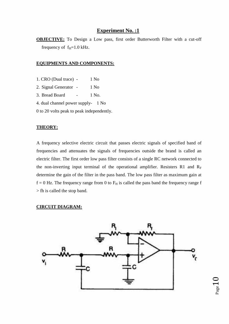
Experiment No. :1
OBJECTIVE: To Design a Low pass, first order Butterworth Filter with a cut-off
frequency of fH=1.0 kHz.
EQUIPMENTS AND COMPONENTS:
1. CRO (Dual trace) - 1 No
2. Signal Generator - 1 No
3. Bread Board - 1 No.
4. dual channel power supply- 1 No
0 to 20 volts peak to peak independently.
THEORY:
A frequency selective electric circuit that passes electric signals of specified band of
frequencies and attenuates the signals of frequencies outside the brand is called an
electric filter. The first order low pass filter consists of a single RC network connected to
the non-inverting input terminal of the operational amplifier. Resisters R1 and RF
determine the gain of the filter in the pass band. The low pass filter as maximum gain at
f = 0 Hz. The frequency range from 0 to FH is called the pass band the frequency range f
> fh is called the stop band.
CIRCUIT DIAGRAM:

Pag
e11
PROCEDURE:
1. Construct the circuit as shown in circuit diagram.
2. Apply an input sine wave and measure the amplitude of output waveform for
different values of input frequencies.
3. Calculate the gain in dB.
4. Plot the frequency response.
OBSERVATIONS:
CALCULATIONS:
i. 1
2Hf
RC
ii. Ao=1+1
FR
R
GRAPH:
Sl. No Input frequency Output voltage Gain 20 log Vo/Vi
1. 100
2 200
3 500
4. 1kHz
5. 1.5KHz
6. 2.0kHz
7. 5kHz

Pag
e12
RESULT:
i. The cut-off frequency of the low pass filter = kHz
ii.The pass band gain of low pass filter =
CONCLUSION:
i. The working of active low pass filter is observed and the output is plotted.
ii. The frequency response of the low pass filter is plotted on a semi-log graph paper.
iii. It is observed that the gain rolls of at the rate of 20dB per decade at the cut of frequency.
REVIEW QUESTIONS
i.Define an electric filter.
ii.Classify filters
iii.Discuss the disadvantages of passive filters
iv.Why are active filters preferred?
v.List the commonly used filters.
vi.Define pass band and stop band of a filter.
vii.What is roll-off rate of a first order filter?
viii.Why do we use higher order filters?
ix.On what does the damping coefficient of a filter depend?
x.What is sallen key filter?
Pag
e13
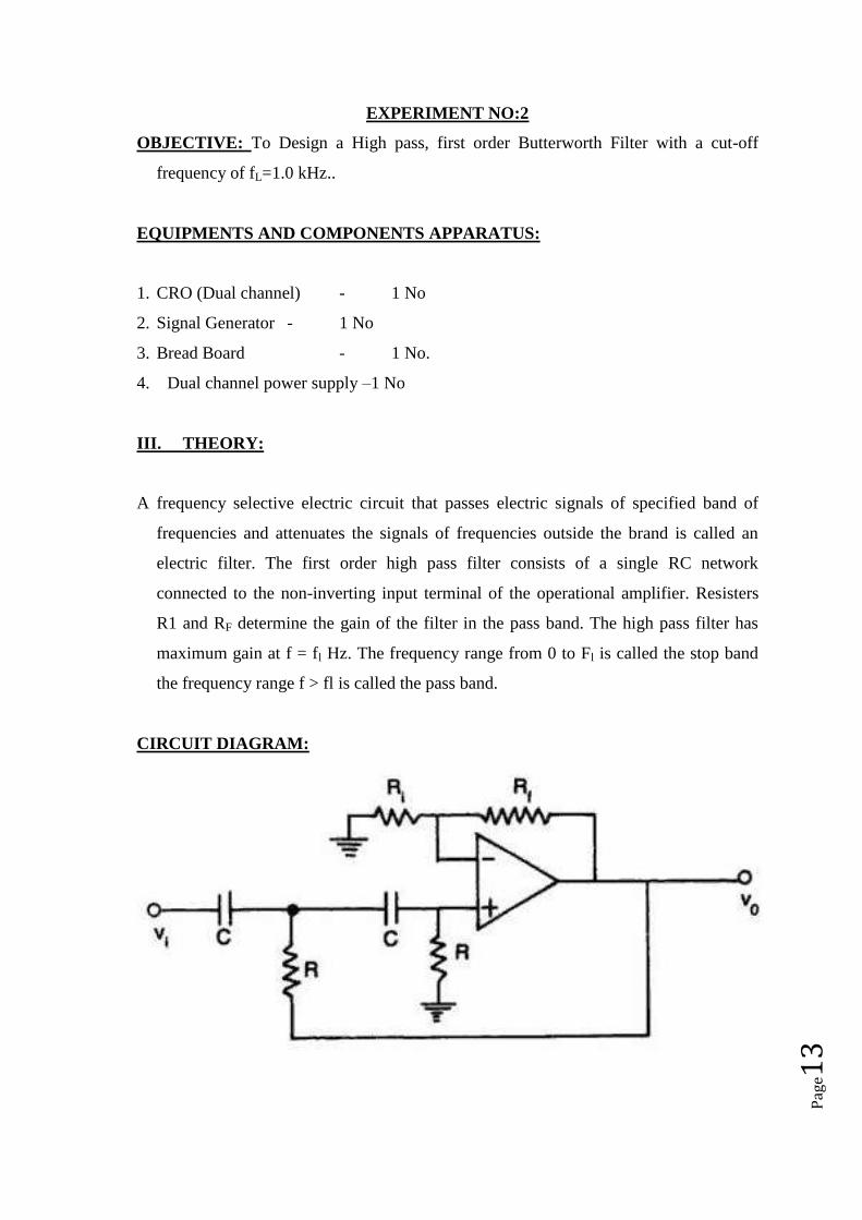
EXPERIMENT NO:2
OBJECTIVE: To Design a High pass, first order Butterworth Filter with a cut-off
frequency of fL=1.0 kHz..
EQUIPMENTS AND COMPONENTS APPARATUS:
1. CRO (Dual channel) - 1 No
2. Signal Generator - 1 No
3. Bread Board - 1 No.
4. Dual channel power supply –1 No
III. THEORY:
A frequency selective electric circuit that passes electric signals of specified band of
frequencies and attenuates the signals of frequencies outside the brand is called an
electric filter. The first order high pass filter consists of a single RC network
connected to the non-inverting input terminal of the operational amplifier. Resisters
R1 and RF determine the gain of the filter in the pass band. The high pass filter has
maximum gain at f = fl Hz. The frequency range from 0 to Fl is called the stop band
the frequency range f > fl is called the pass band.
CIRCUIT DIAGRAM:

Pag
e14
PROCEDURE:
i. Construct the circuit as shown in circuit diagram.
ii.Apply an input sine wave and measure the amplitude of output waveform for different
values of input frequencies.
iii.Calculate the gain in dB.
iv.Plot the frequency response.
OBSERVATIONS:
CALCULATIONS:
i. 1
2Hf
RC
ii. Ao=1+1R
RF
GRAPH:
Sl.No Input frequency Output voltage Gain 20 log Vo/Vi
1. 100
2 200
3 500
4. 1kHz
5. 1.5KHz
6. 2.0kHz
7. 5kHz

Pag
e15
RESULT:
The lower cutoff frequency of the high-pass filter = ------- KHz.
The pass band gain = -------
CONCLUSION:
i. The working of active high pass filter is observed and the output is plotted.
ii. The frequency response of the high pass filter is plotted on a semi-log graph paper.
iii. It is observed that the gain increases at the rate of 20dB per decade at the cut of
frequency.
REVIEW QUESTIONS
i.Define Bessel , Butterworth and Chebyshev filters, and compare their response.
ii.What are the important parameters of a band pass filter?
iii.Define Notch filter.
iv.How do we get a notch filter from a band pass filter?
v.Define state variable filter.
vi.What is switched capacitor ?
vii.Discuss the importance of switched capacitors.
viii.Give the circuit of a switched capacitor low pass filter
ix.Discuss the advantages of active filters
x.What is the roll-off rate of second order filter?

Pag
e16
WEIN BRIDGE OSCILLATOR
AIM: To Design Wein Bridge Oscillator so that the output frequency is 965 Hz.
II EQUIPMENTS AND COMPONENTS:
(i).APPARATUS
1. CRO (Dual channel) - 1 No
2. Bread Board – 1 No
3. Dual Channel Power Supply – 1 No
3. COMPONENTS:
1. 12kΩ Resistor – 1 No.
2. 50kΩ Resistor – 1 No.
3. 3.3kΩ Resistor – 1 No.
4. 0.05F Capacitor – 1 No.
5. Operational Amplifier – 1 No.
III. THEORY:
In this oscillator the Wein Bridge Circuit is connected between the amplifier input terminals and
the output terminal. The bridge has a series RC network in one arm and parallel RC network
in the adjoining arm. In the remaining two arms of the bridge resistors R1 and RF are
connected. The total phase-shift around the circuit is 0o when the bridge is balanced.
IV. CIRCUIT DIAGRAM:

Pag
e17
V. PROCEDURE:
i. Construct the circuit as shown in the circuit diagram.
ii. Adjust the potentiometer Rf such that an output wave form is obtained.
iii. Calculate the output wave form frequency and peak to peak voltage.
iv. Compare the theoretical and practical values of the output waveform frequency.
VI. OBSERVATIONS:
The frequency of oscillation = ______
VII. CALCULATIONS:
The frequency of oscillation fo is exactly the resonant frequency of the balanced Wein Bridge
and is given by fo = 1/ (2RC)
= 0.159 / RC
The gain required for sustained oscillations is given by Av= 3. i.e., Rf = 2R1
Let C = 0.05 F
Then fo = 1/ (2RC)
R = 1/ (2foC)
= 3.3 k

Pag
e18
Now let R1 = 12 k
Then Rf= 2R1 = 24 k
Use Rf = 50 k potential meter.
VIII. GRAPH:
IX: RESULT:
The frequency of oscillation of the Wein Bridge oscillator =----------
X: INFERENCE:
i. The working of Wein Bridge oscillator is observed and the output is plotted.
ii. The frequency response of the Wein Bridge oscillator is plotted
iii. It is observed that the gain doesn’t sustain beyond 5 KHz
i. Design the circuit for different frequencies of oscillations.
XV. REVIEW QUESTIONS
i.State the two condition of oscillations
ii.Classify the oscillators
iii. What is the phase shift in case of the phase shift oscillator?
iv.Explain how to measure the phase difference of two signals
v.In WEIN BRIDGE oscillator what phase shift does the opamp provide?
vi. In what mode the opamp is used in the wein bridge oscillator?
vii.What phase shift is provided by the feedback network?
viii.What is the minimum gain that the inverting opamp should have?
ix.For high frequencies which kind of opamp should be used?

Pag
e19
x.What is the condition for so that the oscillations will not die out?

Pag
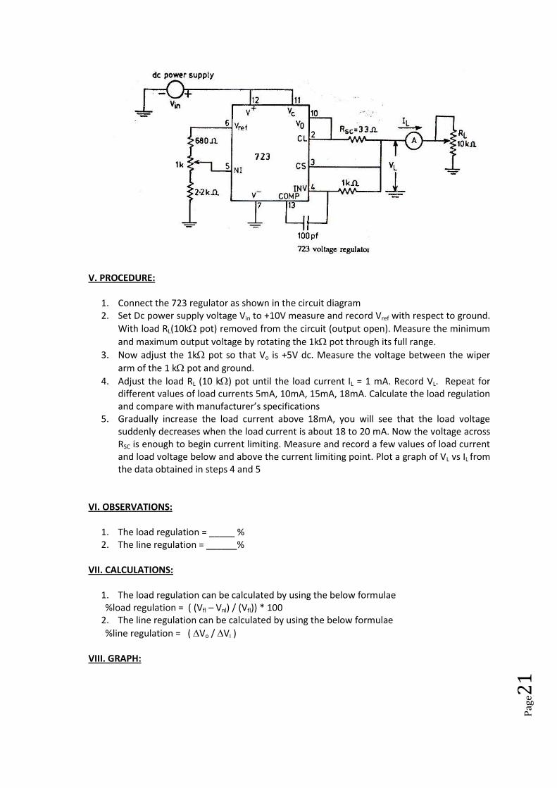
e20
IC 723 VOLTAGE REGULATOR EXPERIMENT NO:5 I AIM: To study the operation of IC723 voltage regulator II EQUIPMENTS AND COMPONENTS: (i).APPARATUS 1. DC power supply - 1 No. 2. Digital Multimeter - 1 No. 3. Ammeter - 1 No. 4. Bread Board - 1 No. . 3. COMPONENTS: 1. 1kΩ Resistor – 1 No. 2. 33Ω Resistor – 1 No. 3. 10k Ω Resistor – 1 No
4. 680 Resistor – 1 No.
5. 2.2 k Resistor – 1 No. 6. 100 pF Capacitor – 1 No 7. IC723
III. THEORY: The three-terminal regulators have the following limitations
1. No short-circuit protection 2. Output voltage (+ve or –ve) is fixed
These limitations have been overcome in 723 general purpose regulator. This IC is inherently
low current device but can be boosted to provide 5 amps or more current by connecting external components. The limitation of 723 is that it has no in-built thermal protection. It also has no short-circuit current limits. The IC723 has two sections. The first section consists of Zener Diode constant current source and a reference amplifier. The other section of the IC consists of an error amplifier series pass transistor and a current limit transistor. This is a 14-pin DIP package. The main
Features of 723 include an input voltage of 40v max, output voltage is adjustable from 2V to 37V, 150 mA output current without external pass resistor, can be used as either a linear or a switching regulator.
IV. CIRCUIT DIAGRAM:
Pag
e21
V. PROCEDURE:
1. Connect the 723 regulator as shown in the circuit diagram 2. Set Dc power supply voltage Vin to +10V measure and record Vref with respect to ground.
With load RL(10k pot) removed from the circuit (output open). Measure the minimum
and maximum output voltage by rotating the 1k pot through its full range.
3. Now adjust the 1k pot so that Vo is +5V dc. Measure the voltage between the wiper
arm of the 1 k pot and ground.
4. Adjust the load RL (10 k) pot until the load current IL = 1 mA. Record VL. Repeat for different values of load currents 5mA, 10mA, 15mA, 18mA. Calculate the load regulation and compare with manufacturer’s specifications
5. Gradually increase the load current above 18mA, you will see that the load voltage suddenly decreases when the load current is about 18 to 20 mA. Now the voltage across RSC is enough to begin current limiting. Measure and record a few values of load current and load voltage below and above the current limiting point. Plot a graph of VL vs IL from the data obtained in steps 4 and 5
VI. OBSERVATIONS:
1. The load regulation = _____ % 2. The line regulation = ______%
VII. CALCULATIONS:
1. The load regulation can be calculated by using the below formulae %load regulation = ( (Vfl – Vnl) / (Vfl)) * 100
2. The line regulation can be calculated by using the below formulae
%line regulation = ( Vo / Vi ) VIII. GRAPH:

Pag
e22
IX: RESULT: i.The % load regulation = ii. The % line regulation = X: INFERENCE: i. The working of 723 regulator is observed and the output is plotted. ii. The load regulation is calculated iii. The line regulation is calculated XV REVIEW QUESTIONS i.What is the maximum input voltage that we can give to 723 regulator? ii.What output voltage range we can obtain from 723 regulator? iii.What is the output current in case of 723 regulator? iv.What are the applications of 723 regulator? v.Define line regulation vi.Define load regulation vii.Define ripple rejection viii.Define long term stability ix.What is the current limit protection x.What are the ideal values of load and line regulations
Pag
e23
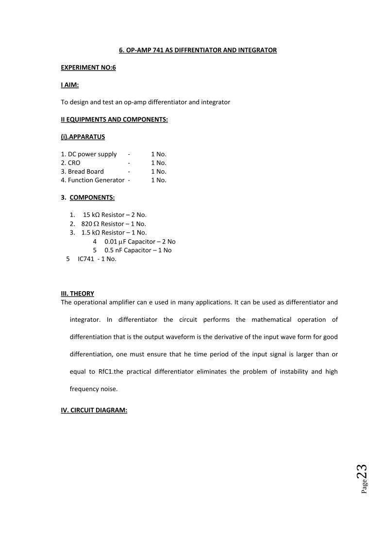
6. OP-AMP 741 AS DIFFRENTIATOR AND INTEGRATOR
EXPERIMENT NO:6 I AIM: To design and test an op-amp differentiator and integrator II EQUIPMENTS AND COMPONENTS:
(i).APPARATUS 1. DC power supply - 1 No. 2. CRO - 1 No. 3. Bread Board - 1 No. 4. Function Generator - 1 No. 3. COMPONENTS:
1. 15 kΩ Resistor – 2 No.
2. 820 Resistor – 1 No. 3. 1.5 kΩ Resistor – 1 No.
4 0.01 F Capacitor – 2 No 5 0.5 nF Capacitor – 1 No
5 IC741 - 1 No. III. THEORY The operational amplifier can e used in many applications. It can be used as differentiator and
integrator. In differentiator the circuit performs the mathematical operation of
differentiation that is the output waveform is the derivative of the input wave form for good
differentiation, one must ensure that he time period of the input signal is larger than or
equal to RfC1.the practical differentiator eliminates the problem of instability and high
frequency noise.
IV. CIRCUIT DIAGRAM:

Pag
e24
V. PROCEDURE: 1 connect the differentiator circuit as shown in fig 1.adjust the signal generator to produce a 5
volt peak sine wave at 100 Hz.
2 observe input Vi and Vo simultaneously on the oscilloscope measure and record the peak
value of Vo and the phase angle of Vo with respect to Vi.
3.Repeat step 2 while increasing the frequency of the input signal. Find the maximum frequency
at which circuit offers differentiation. Compare it with the calculated value of fa Observe &
sketch the input and output for square wave.
4. Connect the integrator circuit shown in Fig2. Set the function generator to produce a square
wave of 1V peak-to-peak amplitude at 500 Hz. View simultaneously output Vo and Vi.
5. Slowly adjust the input frequency until the output is good triangular waveform. Measure the
amplitude and frequency of the input and output waveforms.
6. Verify the following relationship between R1Cf and input frequency for good integration f>fa
& T< R1C1
Where R1Cf is the time constant
7. Now set the function generator to a sine wave of 1 V peak-to-peak and frequency 500 Hz.
Adjust the frequency of the input until the output is a negative going cosine wave. Measure
the frequency and amplitude of the input and output waveforms.
VI. OBSERVATIONS:
1. The time period and amplitude of the output waveform of differentiator circuit 2. The time period and amplitude of the integrator waveform
VII. CALCULATIONS:
Design a differentiator to differentiate an input signal that varies in
frequency from 10 Hz to 1 kHz.
12
1
CRf
f
a
fa = 1 kHz, the highest frequency of the input signal

Pag
e25
Let C1 = 0.01 F,
Then Rf = 15.9 k
Therefore choose Rf = 15.0 k
112
1
CRf a
Choose: fb= 20x fa = 20 KHz
Hence R1 = 795
Therefore choose R1 = 820 Since R1C1 = Rf Cf (compensated attenuator) Cf = 0.54 nF Therefore choose Cf = 0.5nF Integrator: Design an integrator that integrates a signal whose frequencies are between 1 KHz
and 10 KHz
f
bCR
f12
1
the frequency at which the gain is 0 dB.
ff
aCR
f2
1
fa: Gain limiting frequency, The circuit acts as integrator for frequencies between fa and fb Generally fa < fb [ Ref. Frequency response of the integrator] Therefore choose fa = 1KHz Fb = 10 KHz
Let Cf = 0.01 F
Therefore R1= 1.59k
Choose R1= 1.5 K
Rf = 15 K VIII. GRAPH:
Differentiator

Pag
e26
Integrator

Pag
e27
IX: RESULT: Differentiator
______2
1
1
f
bCR
f
T> Rf C1 = _______ Integrator
ff
aCR
f2
1 = _______
T = _________ X: INFERENCE: i. The working of differentiator and integrator is observed and the output is plotted. ii. The time period of the output waveform is calculated iii. The maximum frequency of differentiation and integration is observed
XV REVIEW QUESTIONS
i.Define differentiator ii.Define integrator iii.What are the limitations of an ordinary differentiator? iv. Explain how the practical differentiator will overcome the limitations v.What are the limitations of an ideal integrator? vi.What are the initial conditions of a loss integrator? vii.What are the differences between integrator and differentiator viii.State the applications of integrator ix.State the applications of differentiator x.Explain why integrators are preferred over differentiators in analog computer.
Pag
e28
7. 555 TIMER-ASTABLE MULTI-VIBRATOR EXPERIMENT NO:7 I AIM: To design and test astable multi-vibrator with fixed and adjustable duty cycle. II EQUIPMENTS AND COMPONENTS: (i).APPARATUS 1. DC power supply - 1 No. 2. CRO - 1 No. 3. Bread Board - 1 No. 3. COMPONENTS: 1. 3.62 kΩ Resistor – 1 No. 2. 7kΩ Resistor – 1 No.
3. 0.1 F Capacitor – 1 No 4. IC555 - 1 No. 5. Diode – 1 No.
III. THEORY: The 555 timer can be used with supply voltage in the range of + 5 v to + 18 v and can drive upto
200 mAmps. It is compatible with both TTL and CMOS logic circuits because of the wide range of supply voltage the 555 timer is versatile and easy to use in the astable multivibrator. The timer is oscillated between two threshold levels 1/3 Vcc and 2/3 Vcc in order to generate a square wave form. No external signal source is required for such generation and hence this is called as a free running multivibrator.
IV. CIRCUIT DIAGRAM:

Pag
e29
V. PROCEDURE: i.Connect the circuit using the component values as per the design of part – i ii.Observe and sketch the capacitor voltage wave form (pin-6) and output waveform (pin-3)
measure the frequency and duty cycle of the output wave form iii.Connect the circuit of fig2 using component values as per the design of part – ii and repeat
the step 2 by adjusting both the potential meters for duty cycle of 10%, 50% and 90% with a frequency of 1kHz.
VI. OBSERVATIONS: 1.tON = 69 (RA + RB) C 2.tOFF = 0.69 RBC
3. 100% xtt
tDutycycle
OFFON
ON
VII. CALCULATIONS: i. Design of astable multi-vibrator of 1 kHz with a 75% duty cycle tON = 69 (RA + RB) C tOFF = 0.69 RBC
100100% xT
tx
tt
tDutycycle ON
OFFON
ON
Where T = 1/f, the time period of the output waveform T= 1msec, tON = 0.75 m/sec, tOFF 0.25msec
Lec C = 0.1 F
RB = 3.62 k
Choose RB = 1.8 k + 1.8 k
cRRTf
BA )2(
45.11
Eq. (1)
ii. Design of astable multivibrator to produce 1 KHz output waveform with adjustable duty cycle of 10% to 90%
The circuit is as shown in Fig. 2 During the charging period, the diode ‘D’ is forward biased, RB is bypassed Hence ton = 0.69 RAC.

Pag
e30
During the discharge period, the discharging transistor is shorted (ON) and the diode ‘D’ is reverse biased.
Hence tOFF = 0.69RB C Output frequency f= 1 KHz is assumed
cRRTf
BA )(
45.11
Eq. (2)
Let C = 0.1 F
RA + RB = 14.5 K Where tON= 0.1 m/sec (for 10% duty cycle)
RA= 1.44 K When tON = 0.9 m/sec (for 90% duty cycle)
RA = 12.96 K
RA is to be varied form 1.414 K to 12.96K for 10% to 90% duty cycle.
Therefore choose RA as 1.0 K fixed resistor + 15.0k pot, similarly RB VIII. GRAPH:
IX: RESULT: tON = 69 (RA + RB) C = tOFF = 0.69 RBC =
100100% xT
tx
tt
tDutycycle ON
OFFON
ON
=
X: INFERENCE: i. The working of 555 timer astable multivibrator is observed and the output is plotted. ii. The duty cycle is calculated iii. Frequency of the output wave form is calculated
XV REVIEW QUESTIONS

Pag
e31
i.Explain the functional block diagram of a 555 timer ii.Explain the function of reset iii.What are the modes of operation of timer? iv.What is the expression of time delay of a astable multivibrator? v.Discuss some applications of timer in astable mode. vi.Define duty cycle vii.Give methods of obtaining symmetrical waveform. viii.How is an astable multivibrator connected into a pulse position modulator ix.How Schmitt trigger circuit is constructed using 555 timer x.Draw the pin diagram of 555 timer.

Pag
e32
8.555 TIMER-MONOSTABLE MULTI-VIBRATOR EXPERIMENT NO:8 I AIM: To design and test monostable multi-vibrator using IC555 Timer. II EQUIPMENTS AND COMPONENTS: (i).APPARATUS 1. DC power supply - 1 No. 2. CRO - 1 No. 3. Bread Board - 1 No. 4. Function Generator - 1 No.
3. COMPONENTS: 1. 11.8 kΩ Resistor – 1 No. 2. 1kΩ Resistor – 1 No.
3. 0.1 F Capacitor – 1 No
4. 0.01 F Capacitor – 1 No 5. IC555 - 1 No. 6. 1N4148 Diode – 1 No.
III. THEORY: The 555 timer can be used with supply voltage in the range of +5 v to +18 v and can drive upto
200 mAmps. It is compatible with both TTL and CMOS logic circuits because of the wide range of supply voltage the 555 timer is versatile and easy to use in monostable multivibrator we will provide external triggering in order to make the timer to switch over to high state (unstable). This is also called as one-short multivibrator.
IV. CIRCUIT DIAGRAM:

Pag
e33
V. PROCEDURE:
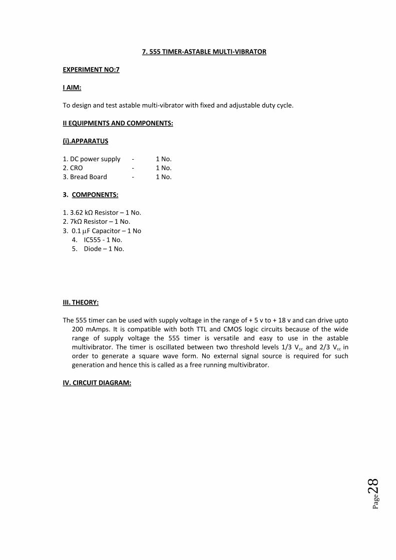
1. Connect the circuit using the component values as per the design 2. Set the square wave 2.5V peak and 1KHz trigger input on function generator 3. Apply the trigger input at pin-2 through capacitor C1. Observe both trigger input and the
output of the multivibrator on CRO simultaneously and sketch the waveforms 4. Repeat the step 3 for trigger input of 2KHz frequency
VI. OBSERVATIONS: 1 TP = 1.1 R.C. = 1.3 m/sec 2. T = 1/ f = 1m/sec VII. CALCULATIONS: i. To produce a pulse of 1.3 m/sec duration: TP = 1.3mSec TP = 1.1 R.C.
Let C = 0.1 F
R = 11.8K To provide negative edge triggering a circuit of fig.2 is to be connected between pin 2 and 8. Design of Differentiator: Let the trigger input frequency is 1KHz i.e., T = 1/f = 1mSec
Assume 1 = R1 C1 = 0.01mSec
Let C = 0.01 F
Therefore R1 = 1.0 K VIII. GRAPH:
Pag
e34
IX: RESULT: Tp = 1.1R.C. = X: INFERENCE:
i. The working of 555 timer monostable multivibrator is observed and the output is
plotted.
ii. The time period of the output waveform is calculated iii. Frequency of the output wave form is calculated
XV REVIEW QUESTIONS i. Explain the functional block diagram of a 555 timer ii. Explain the function of reset iii. What are the modes of operation of timer? iv. What is the expression of time delay of a monostable multivibrator? v. Discuss some applications of timer in monostable mode. vi. Define duty cycle vii. Give methods of obtaining symmetrical waveform. viii.How is an monostable multivibrator connected into a pulse position modulator ix. How Schmitt trigger circuit is constructed using 555 timer x. Draw the pin diagram of 555 timer.

Pag
e35
9. IC565 PLL EXPERIMENT NO:9 I AIM:
1. To study the operation of NE565 PLL 2. To use NE565 as a multiplier
II EQUIPMENTS AND COMPONENTS:
(i).APPARATUS 1. DC power supply - 1 No. 2. CRO - 1 No. 3. Bread Board - 1 No. 4. Function Generator - 1 No. 3. COMPONENTS: 1. 6.8 kΩ Resistor – 1 No.
2. 0.1 F Capacitor – 1 No
5. 0.001 F Capacitor – 2 Nos 6. IC565 - 1 No.
III. THEORY: The 565 is available as a 14-pin DIP package. It is produced by signatic corporation. The output
frequency of the VCO can be rewritten as
HzCR
fTT
o
25.0
where RT and CTare the external resistor and capacitor connected to pin 8 and pin 9. A value
between 2 k and 20 k is recommended for RT. The VCO free running frequency is adjusted with RT and CT to be at the centre fo the input frequency range.
IV. CIRCUIT DIAGRAM:

Pag
e36
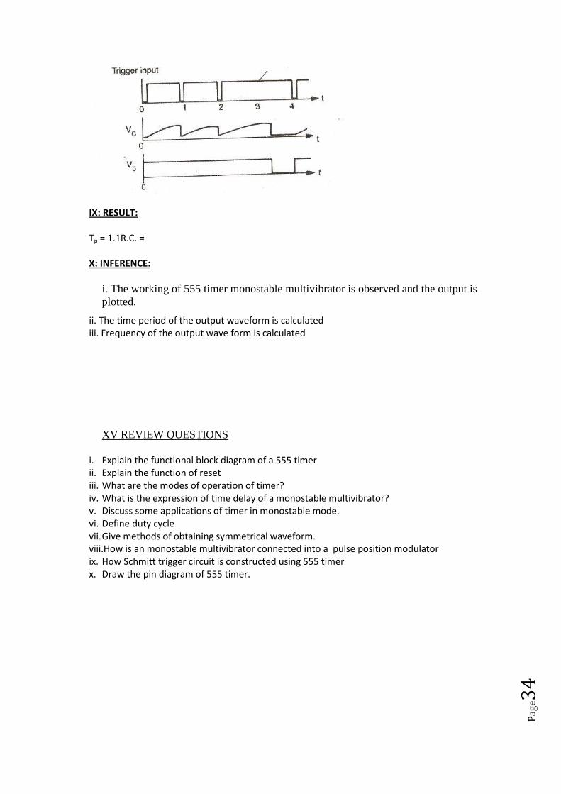
V. PROCEDURE: i. Connect the circuit using the component values as shown in the figure ii .Measure the free running frequency of VCO at pin 4 with the input signal Vin set = zero.
Compare it with the calculated value = 0.25/ RTCT iii. Now apply the input signal of 1Vpp square wave at a 1kHz to pin 2 iv. Connect 1 channel of the scope to pin 2 and display this signal on the scope v .Gradually increase the input frequency till the PLL is locked to the input frequency. This
frequency f1gives the lower ends of the capture range. Go on increase the input frequency, till PLL tracks the input signal, say to a frequency f2. This frequency f2 gives the upper end of the lock range. If the input frequency is increased further the loop will get unlocked.

Pag
e37
vi. Now gradually decrease the input frequency till the PLL is again locked. This is the frequency f3, the upper end of the capture range. Keep on decreasing the input frequency until the loop is unlocked. This frequency f4 gives the lower end of the lock range
vii .The lock range fL = (f2 – f4) compare it with the calculated value of 12
8.7 fo
Also the capture range is fc = (f3 – f1). Compare it with the calculated value of capture range. 2/1
3 ))10)(6.3)(2(
xC
ff L
c
viii. To use PLL as a multiplie5r, make connections as showin in fig. The circuit uses a 4-bit binary counter 7490 used as a divide-by-5 circuit.
ix. Set the input signal at 1Vpp square wave at 500Hz
x.. Vary the VCO frequency by adjusting the 20K potentiometer till the
PLL is locked. Measure the output frequency
xi. Repeat step 9 and 10 for input frequency of 1kHz and 1.5kHz.
VI. OBSERVATIONS: fo = __________ fL = __________ fC = __________ VII. CALCULATIONS:
fL = (f2 – f4) = 12
8.7 fo
fc = (f3 – f1) =
2/1
3 ))10)(6.3)(2(
xC
f L
VIII. GRAPH:
Pag
e38
IX: RESULT: fo = __________ fL = __________ fC = __________ X: INFERENCE: i. The working of 565 PLL is observed and the output is plotted. ii. The time period of the output waveform is calculated iii. Frequency of the output wave form is calculated iv. The Lock range and Capture range of the PLL are calculated.
XV REVIEW QUESTIONS
i. List the basic building blocks of a PLL. ii. Define capture range iii. Define lock range iv. Define pull in time

Pag
e39
v. Which is greater capture range or lock range? vi. What is the major difference between digital and analog PLLs vii. List the applications of PLL,
viii.Explain about phase detector ix. Explain about PLL based AM detector x. Explain the operation of multiplier circuit.

Pag
e40
10. IC566 VCO EXPERIMENT NO:10 I AIM: To study the operation of NE566 VCO II EQUIPMENTS AND COMPONENTS:
(i).APPARATUS 1. DC power supply - 1 No. 2. CRO - 1 No. 3. Bread Board - 1 No. 4. Function Generator - 1 No. 3. COMPONENTS: 1. 6.8 kΩ Resistor – 1 No. 2. 15 kΩ Resistor – 1 No. 3. 100 kΩ Resistor – 1 No. 4. 75 pF Capacitor – 1 No 5. IC566 - 1 No. . III. THEORY: A common type of VCO available in IC form in Stigmatic NE/SE566. Referring to the circuit
diagram a timing capacitor CT is linearly charged or discharged by a constant current source/sink. The amount of current can be controlled by changing the voltage vc applied at the modulating input (pin5) or by changing the timing resistor RT external to IC chip. The voltage at pin 6 is held at the same voltage as pin 5. Thus, if the modulating voltage at pin5 is increased, the voltage pin 6 also increases, resulting in less voltage across RT and thereby decreasing the charging current.
The voltage across the capacitor CT is applied to the inverting input terminal of Schmitt Trigger
the output voltage swing of the Schmitt Trigger is designed to Vcc and 0.5 Vcc. The output
frequency of the VCO can be calculated as follows:
The total voltage on the capacitor changes from 0.25 Vcc to 0.5 Vcc. Thus v = 0.25 Vcc. The
capacitor charges with a constant current source.
So, TC
i
t
v
TC
i
t
Vcc
25.0

Pag
e41
t = i
VccCT25.0
The time period T of the triangular wave form equal to 2t. The frequency of oscillator fo is,
fo = tT
2
11
= TCVccC
i
5.0
But i = T
CC
R
VcV
Where Vc is the voltage at pin 5. Therefore,
fo = CCTT
CC
VRC
VcV )(2
The output frequency of the VCO can be changed either by (i) RT, (ii) CT are (iii) The voltage VC at the modulating input terminal pin 5. The voltage VC can be varied by connecting a R1R2 circuit.
IV. CIRCUIT DIAGRAM:
V. PROCEDURE:
1) Make connections of the VCO as show in the Circuit diagram. 2) Measure the free running frequency of VCO at Pin 4, with the input signal V in set = 0.
Compare it with the theoretical calculated value. 3) Draw the output wave form obtained at Pin No 3. 4) Draw the output wave form obtained at Pin No 4 5) Compare the theoretical and practical values of free running frequency.
Pag
e42
VI. OBSERVATIONS:
fo = CCTT
CC
VRC
VcV )(2 = ___________
Output amplitude at Pin 4 = _____________ Output amplitude at Pin 3 = _____________ VII. CALCULATIONS:
TC
i
t
v
TC
i
t
Vcc
25.0
t = i
VccCT25.0
The time period T of the triangular wave form equal to 2t. The frequency of oscillator fo is,
fo = tT
2
11
= TCVccC
i
5.0
But i = T
CC
R
VcV
Where Vc is the voltage at pin 5. Therefore,
fo = CCTT
CC
VRC
VcV )(2
VIII. GRAPH:

Pag
e43
IX: RESULT: fo = _________ X: INFERENCE: i. The working of 566PLL is observed and the output is plotted. ii. The time period of the output waveform is calculated iii. Frequency of the output wave form is calculated
XV REVIEW QUESTIONS i. List the basic building blocks of a VCO. ii. Define free running frequency. Iii .Define lock range Iv .Explain the block diagram of IC 566 VCO. v. What is the range of modulating input voltage applied to a VCO? vi. What is the frequency transfer coefficient of VCO. vii. List the applications of VCO, viii. Explain about Schmitt trigger circuit. Ix .Explain how VCO is used in PLL. X .Explain the operation of constraint current source.

Pag
e44
11. COMPARATOR
EXPERIMENT NO: 11 I AIM: To Study the operation of comparator II EQUIPMENTS AND COMPONENTS:
(i).APPARATUS 1. DC power supply - 1 No. 2. CRO - 1 No. 3. Bread Board - 1 No. 4. Function Generator - 1 No. 3. COMPONENTS: i.10 kΩ Resistor – 1 No.
ii.1k Resistor – 1 No. iii.IC741 - 1 No. . III. THEORY: A comparator is a circuit which compares a signal voltage applied at one input of an OPAMP
with a known inference voltage at the other input. It is basically an open loop OPAMP with
output Vsat . It may be seen that change in output state takes place with an increment in input Vi of only 2mV. There are basically two types of comparators, non-inverting comparator and inverting comparator.
IV. CIRCUIT DIAGRAM:

Pag
e45
V. PROCEDURE:
1. Connect the circuit shown in Fig. And adjust the 10 k potentiometer so that Vref = +0.5V 2. Adjust the signal generator so that vi = 2V pp sine wave at 1 kHz. 3. Using a CRO observe the input and output waveform simultaneously. Plot the output waveform.
4. Adjust the 10 k potentiometer so that Vref = -0.5V. Repeat step 3 5. To make a zero crossing detector, set Vref = 0V and observe the output waveforms.
VI. OBSERVATIONS:
1. Vout = _________
2. Vin = _________

Pag
e46
VII. CALCULATIONS: Vref = 0.5 V VO = ________ Vref = -0.5V VO = _______ Time period of output waveform = ___________ VIII. GRAPH:
IX: RESULT: Vin = _______ VO = _______ Vref = ________ X: INFERENCE: i. The working of comparator is observed and the output is plotted. ii. The time period of the output waveform is calculated iii. Frequency of the output wave form is calculated

Pag
e47
XV. REVIEW QUESTIONS i.Discuss the characteristics of an ideal comparator. ii.List the different types of comparators. iii.What is the meaning of Voltage limiting? iv.What is window detector? v.What is zero crossing detector? vi.What is Schmitt trigger circuit? vii.What is time maker generator? viii.What are the differences between ideal and practical comparator? ix.What are the applications of comparator? x. In which mode the operational amplifier is connected in the comparator circuit.

Pag
e48
12. D/A CONVERTER EXPERIMENT NO:12 I AIM: To construct a 4-bit R – 2 R ladde type D/A converter. Plot the transfer characteristics, that is,
binary input vs output voltage. Calculate the resolution and linearity of the converter from the graph.
II EQUIPMENTS AND COMPONENTS:
(i).APPARATUS 1. DC power supply - 1 No. 2. CRO - 1 No. 3. Bread Board - 1 No. 4. Function Generator - 1 No.
3. COMPONENTS: 1.10 kΩ Resistor – 1 No.
2.20 k Resistor – 1 No. 3.IC741 - 1 No.
.Bandwidth adjustment range = < 1 to 60% III. THEORY: Most of the real world physical quantities such as voltage current temperature pressure are
available in analog form. It is very difficult to process the signal in analog form, hence ADC and DAC are used. The DAC is to convert digital signal into analog and hence the functioning of DAC is exactly opposite to that of ADC. The DAC is usually operated at the same frequency as the ADC. The output of the DAC is commonly staircase. This staircase like digital output is passed through a smoothing filter to reduce the effect of quantization noise. There are three types of DAC techniques (i) Weighted resistor DAC (ii) R-2R ladder. (iii) Inverted R-2R ladder. Wide range of resistors is required in binary weighted resistor type DAC. This can be avoided by using R-2R ladder type DAC where only two values of resistors are required it is well suited for integrated circuit realization.
IV. CIRCUIT DIAGRAM:

Pag
e49
V. PROCEDURE:
i. Set up the circuit shown in Fig.
ii. With all inputs (d0 to d3) shorted to ground, adjust the 20 k pot until
the output is 0V. This will nullify any offset voltage at the input of the op-
amp. Iii ..Measure the output voltage for all binary input states (0000 to 1111) and plot a graph of
binary inputs vs output voltage. iv. .Measure the size of each step and hence calculate resolution v. .Calculate linearity
VI. OBSERVATIONS:
Output Voltage = ____________ Size of each step = ____________ Resolution = ____________ Linearity = ____________ VII. CALCULATIONS: VO = VR / 2 = VFS / 2 Resolution (in volts) = VFS / (2n –1) = 1 LSB increment. VIII. GRAPH:

Pag
e50
. IX: RESULT: Output Voltage = ____________ Size of each step = ____________ Resolution = ____________ Linearity = ____________ X: INFERENCE: i. The working of D / A converter is observed and the output is plotted. ii. The staircase wave form is plotted. iii. Resolution is calculated.
XV REVIEW QUESTIONS i. Classify DAC on the basis of their output. ii. Name the essential parts of a DAC. iii. Describe the various types of electronic switches used in DAC. vi. How many resistors are required in 12 bit weighted resistor DAC? v. Why is an inverted R-2R ladder network DAC is better than R-2R ladder DAC. vi. Define resolution. vii. Define linearity. Viii .Define monotonicity. Ix .Define step size. x. Define settling time.