Afl-AOG IBM THOMAS J WATSON RESEARCH … 67 IBM THOMAS J WATSON RESEARCH CENTER YORKTOWN HEIGHTS MY...
38
/Afl-AOG 67 IBM THOMAS J WATSON RESEARCH CENTER YORKTOWN HEIGHTS MY F/6 20/12 SPECTROSCOPIC STUIES OF THE ELECTRONIC STRUCTURE OF METAL-SEI-ETC(U) 8AR 80 0 E EASTMAN F4620-76fC-00I tICLASSIFIED AFOSR-TR-80-0455 M I fllIllllfffffff
-
Upload
truongkiet -
Category
Documents
-
view
221 -
download
0
Transcript of Afl-AOG IBM THOMAS J WATSON RESEARCH … 67 IBM THOMAS J WATSON RESEARCH CENTER YORKTOWN HEIGHTS MY...
/Afl-AOG 67 IBM THOMAS J WATSON RESEARCH CENTER YORKTOWN HEIGHTS MY F/6 20/12SPECTROSCOPIC STUIES OF THE ELECTRONIC STRUCTURE OF METAL-SEI-ETC(U)
8AR 80 0 E EASTMAN F4620-76fC-00ItICLASSIFIED AFOSR-TR-80-0455 M
I fllIllllfffffff

AFOSR-TR. 8O0 04 5 5/~
SPECTROSCOPIC STUDIES OF THE ELECTRONIC STRUCTURE OF
METAL-SEMICONDUCTOR AND VACUUM-SEMICONDUCTOR INTERFACES
Dean E. Eastman
___ IBM Thomas J. Watson Research Center00J P.O. Box 218
Yorktown Heights, New York 10598
March 24, 1980
Final Technical Report for the Period October 1, 1976 - October 31, 1979
Contract No. F44620-76-C-0041
Approved for public release, distribution unlimited.
Prepared for:
Air Force Office of Scientific Research(AFSC)
Bldg. 410, Boiling AFB, D.C. 20332
* r~~JUN74c~ :~ir. '
l's...L
unclassifiee'
EECURITY CLASSIFICATON O ETTIS PAGE READ INSTRUCTIONS
EPORT DOCUMENTATION PAGE BEFORE COIPLETING FORM
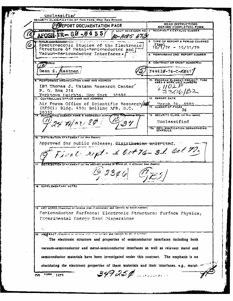
,- 4 5 2 GOVT ACCESSION NO. 3. RECIPIENT'S CATALOG NUMBER
.. -- . TYPE OF REPORT & PERIOO COVERED
Spectroscopic Stdies of the Electron'u li/1 /
Structure o. ;etal-,eiconductor and0 " _ _I0/I/7_ - 10/31/79
Vac'au-Seyniconductor Interfaces* 6. PERFORMING ORG. REPORT NUMBER
. R 8). CONTRACT OR GRANT NUMBER(s)
Dean E. astnan / F 62-76-C-
9. PERFORMING ORGANIZATION NAME AND ADDRESS 10. PROGRAM ELEMENT. PROJECT. TASKAREA & WORK UNIT NUMBERS
IBMr Thomas J. W1atson Research Center / // FP. 0. Box 218 ',)O&/FYorktown K:eichts, :.w York 1I059P __-..,(____ ,.._._..._I_
It. CONTROLLING OFFICE NAME AND ADDRESS 12. REPORT DATE
Air Force Office of Scientific Research/N '<rth MU O1(AFSC) ; Bldg. 410; Bolling AFB, D.C. 33 NUMBEROFPAES620332
14. MONTRIG AGE.4C./Nt AM & ADDRESS(A! dllersp - r11 e) IS. SECURITY CLASS. (of this report)
Con Unclassified
. .ISa. DECLASSIFICATION,'DOWNGRADINGSCHEDULE
1S. DISTHIBUTION STATEMENT (of this Report)
Approved for public release?, i ib --t .,ltwtd.
17. r-R(of the-I tt'liWTok 20, It differ'ent fro Report)
18. SUPPLEMENTARY NOTES
19. KEY WOROS (Continue on reverse side it necessary and Identify by block number)
Fer-iconductor Surfaces; Electronic Structure; Surface Physics;f::nerinental Enerav Band Dispersions
20. ABq RACT (Cnnfn.,,- 11 r-,'e. ' f -P. srv and identify h- bl.k .- ter'
The electronic structure and properties of semiconductor interfaces including both
vacuum-semiconductor and metal-semiconductor interfaces as well as relevant metal and
semiconductor materials have been investigated under this contract. The emphasis is on
elucidating the electronic properties of these materials and their interfaces, e.g., metal-
, R . .172 .- -
-anc lnss i ,. i.d
SECURITY CLASSIFICATION OF 'THIS PAGE(WIhe Data Ente'sd) ,
semiconductor Schottky barriers, which are of far reaching importance in such semiconductor
devices as MOSFETS, CCD devices, photovoltaic devices, etc. W; e p:f-erm extensive
studies of the electronic structure of semiconductor surfaces and interfaces and related metal
surfaces as a function of surface preparation, doping, thickness of adsorbed overlayer, etc.
The probes we have used include photoelectron spectroscopy (XPS and UPS - with an
emphasis on angle-resolved studies using synchrotron radiation) and yield spectroscopy,
electron energy loss spectroscopy, low energy electron diffraction and theoretical band
structure methods. Our research has included studies of well characterized surfaces of silicon
and gallium arsenide, of silicides and Si-silicide interfaces, of bulk Ge, GaAs and GaSb, of Ni
and Co surfaces, of bulk Ni, Cu, Fe, Co, ThH 2, Zn and LaB6 materials. A major achievement
of our research program has been the development for the first time of accurate experimental
methods for determining the electron energy vs momentum band dispersions E() of materials
and their surfaces; such E(f) dispersions are of central importance in solid state physics in
understanding the electronic, physical and chemical properties of materials.
lincln qi f it-0
3
TABLE OF CONTENTS
ABSTRACT
1. HIGHLIGHTS
U1. SUMMARY OF WORK COMPLETED UNDER CONTRACT
A. Electronic structure of semiconductor surfaces and interfaces.B. Electronic structure of group IV and
group rn-V semiconductors.C. Electronic structure of metal surfaces.D. Electronic structure of metals and metallic compounds.E. Studies of electronic many-electron effects.
M. LIST OF PUBLICATIONS UNDER CONTRACT
IV. BIOGRAPHY OF PRINCIPAL INVESTIGATOR
AIR F.. V'S ... .
Th : ,API..'" and is
P ' ".. , .' , ,, J0--1- (7b).
A. D.rechznlc K, . c: .,i,.)u Officer

I. HIGHLIGHTS
Significant and extensive progress in understanding the electronic structure and propertiesof semiconductor surfaces and semiconductor interfaces as well as selected metallic andsemiconductor materials has been accomplished under Air Force Office of Scientific ResearchContract F44620-76-C-0041 [Oct.'75-Sept.'79]. Techniques which have been used includephotoelectron spectroscopy (with an emphasis on angle-resolved photoemission using synchro-tron radiation), low energy electron diffraction (LEED), electron energy loss spectroscopy andAuger spectroscopy, as well as realistic band structure calculations for surfaces and bulkmaterials. In summary, 34 research papers have been published under this contract (seeSection III) on the electronic structure of (a) semiconductor surfaces and interfaces, (b) groupIV and rn-V semiconductors, (c) metal surfaces, (d) metals and metallic compounds, and (e)many-electron effects. As selected examples, three major highlights are described in thisSection: (1) New instrumentation-a display analyzer system for photoemission, (2) bandstructure determination of semiconductor surfaces-Si(100)-(2x I) and (3) band structuredetermination of bulk semiconductors--GaAs. A major accomplishment of our researchprogram has been the development for the first time of accurate experimental methods fordetermining the electron energy vs momentum E(f) band dispersions of surfaces and bulkmaterials. Such one-electron band dispersions E(t) are of central importance in solid statephysics in understanding the physical, chemical and electronic properties of materials and theirsurfaces and interfaces.
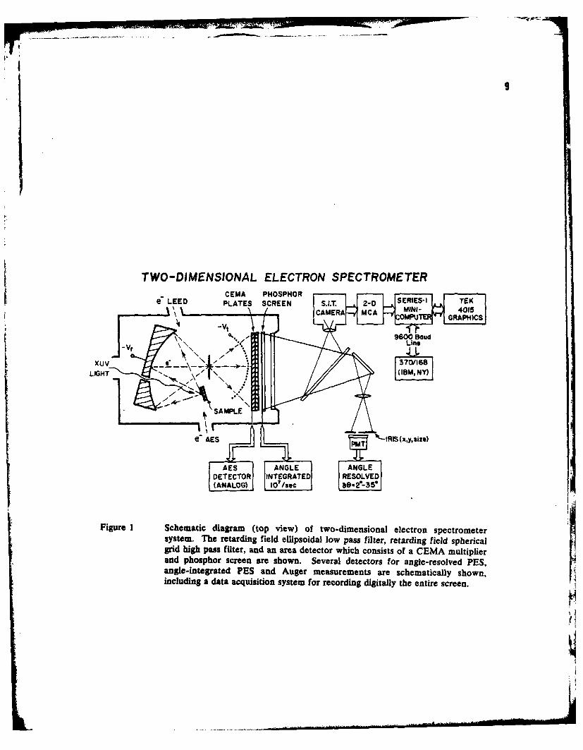
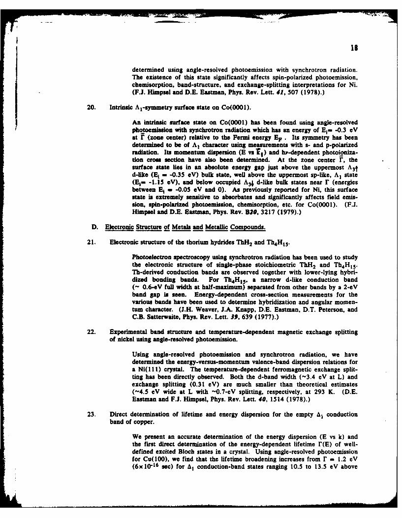
Ellipsoidal Mirror Display Analyzer System for Electron Energy and AngularMeasurements. A new type of electron energy analyzer' (Fig. 1) with full angular display(- 2 steradians) has been conceived and constructed by D.E. Eastman at IBM which issuccessfully operating at the Synchrotron Radiation Center at the University of Wisconsin-Madison. This is the first display-type spectrometer and has, for many types of measurements,an unprecedented performance - better than 100 meV energy resolution and -2" angularresolution with total data rates -100 times greater than other spectrometers. The design anddevelopment were motivated by the objective of constructing a high-resolution analyzer systemcapable of the combined measurements of:
(I) angle-resolved XUV photoemission spectroscopy (ARPES) with a polarized synchro-tron radiation source
(2) angle-integrated XUV photoemission spectroscopy(3) efficient Auger electron spectroscopy (AES)(4) low-energy electron diffraction (LEED).
The primary motivation was ARPES Xith synchrotron radiation, for which the differentialphotoemission cross section N(E,hP,k,ep,n) involves the measurement/control of fourcontinuous variables (electron energy E, photon energy hy, and two independent components
Aof momentum , .e., the angular direction) as well as the polarization e. of the radiation andcrystallographic direction n of the single crystal sample. This new display-type spectrometersystem, which incorporates a separate UHV sample preparation chamber, has been combinedwith a novel TGM monochromator that covers the entire spectral range (5 :< hr : 150 eV) ofthe 240 MeV storage ring radiation source at the University of Wisconsin-Madison. It hasbeen used for several types of angle-resolved and angle-integrated electron spectroscopies -photoemission, Auger, energy loss as well as elastic and inelastic low energy electron diffrac-tion (LEED and ILEED) for about two years with great success. This system has been ofcentral importance in attaining a major achievement: the development of techniques foraccurately determining one-electron band dispersions E(f) for solids and surfaces. Theseresults are summarized in Section MII.

5
A description of the principles of operation and features of the electron imaging two-dimensional display spectrometer system, schematically shown in Fig. 1, is as follows. A topview is depicted in Fig. 1, with hi denoting the radiation (horizontally polarized monochro-matic synchrotron radiation) which enters through a hole in the ellipsoidal mirror at 340 belowthe horizontal plane, e-AES denotes an electron source (- 1-2 keV) for Auger spectroscopy,and e-LEED denotes an electron source (0-400 eV) for LEED studies. Combined energy andangular analyses are achieved by using two retarding fields: an ellipsoidal mirror (V r) used ina reflection mode as a low-pass energy filter, and a spherical 4-grid stage (retard grid shown,V) used in a transmission mode as a high-pass filter. With an energy overlap of the twofilters for electrons emitted in any direction within the acceptance angle of the analyzer (3directions shown), the analyzer transmits electrons only in a narrow energy range AE aboutthe pass energy Ep a eVt. By suitably adjusting Vr and Vt , an energy resolution AE-O. 1 eVor larger can be selected (-lmm diameter source size, Ep-10eV) while accepting the full solidangle. A two-dimensional position-sensitive detector stage follows the high pass filter. Thisconsists of two continuous electron multiplier arrays (CEMA) with a gain of -107 followed bya phosphor screen. The electron pulses (-2ns) leaving the CEMA are accelerated andconverted to light pulses (-108 photons/pulse) at the phosphor screen, which are viewed andrecorded through a viewport. Electrons reaching the detector stage have a one-to-onerelationship between their angulw" direction and detected position.
Two angle-resolved detectors for ARPES are used. Namely, the image on the screen isviewed through a viewport with a beam-splitting mirror while a second mirror and lens forman image of the screen (Fig. 1). There is a single-channel angle-resolved detector (acceptance859,2°-35 full angle) which has an adjustable optical iris in this image plane (x and ycoordinates and size are electronically-controlled) followed by a photomultiplier countingsystem. This detector views a selected direction and digitally counts all electron events withinan acceptance angle 80. Counting rates are typically 104-105 c/s for 80=40-100,&Ea0.1-0.3 eV, and hr-8-50 eV.
The second angle-resolved detector is a two-dimensional digital data acquisition systemwhich utilizes the full capability of the analyzer. As schematically shown in Fig. 1, thisconsists of a silicon-intensified-target (S.I.T.) video camera which records all electron eventsand reads them (video rates of -3.5 megaband pixel rate) into a two-dimensional multichannelanalyzer (2-D MCA) which is controlled by an IBM Series/I computer system that collects,processes, and transfers data pictures to a Tektronix 4015 graphics terminal and to the BM370/168 computer system at IBM Research, Yorktown Heights, New York, over a 9600 baudline. The MCA (Quantex Model DS12) has 256x256m65,536 channels or pixels, each with a12-bit word. Each channel, which corresponds to an angle of -1/3x l/3*, can be operatedin a counting mode or a signal-averaging (ratemeter) mode. Energy distribution "pictures"(EDP's) can thus be taken and stored. Subsequently, angle-resolved energy distributions(AREDC's) for arbitrary directions can be selected from these "EDP's" and viewed. Angle-integrated spectra are simply obtained by summing all pixels of each full picture and plottingeach picture sum versus electron energy.
Electronic Structure of Surfaces-- E(k) Band Dispersions for Si(100)-(2xil Surface.The Si(100) surface is the standard substrate used for MOSFETS and has been studiedextensively. When prepared with a clean surface, Si(100) reconstructs with a (2x 1) surfaceunit mesh, as seen by low energy electron diffraction (LEED). The reconstructed Si(100)-(2x 1) surface has been the subject of many theoretical studies and experimental studies,including photoemission, 2 LEED,3 and electron energy loss spectroscopy. Various structuralmodels have been proposed and studied for this reconstructed surface, including a number ofdifferent pairing models 3 ,'5 s8 t ,1 12 and vacancy models. 5,6,8, 10 ,12 Several different conclusionshave been reached concerning the structure of the Si(100)(2x I) surface via calculations ofLEED3. 12 and photoemisson spectra6,7 and comparison with experimental data. A "zig-zag"

chain model has been proposed which is based on a LEED intensity analysis; 3 a self-consistentsurface calculation for this model yields metallic surface state bands. 7 Self-consistent surfacecalculations have also been performed for a vacancy model and a dimer-like pairing model, 63
as well as for the ideal unrelaxed and unreconstructed surface. 7 ,8 This dimer-ike pairing model
has been suggested as a preferred model, based on a comparison with angle-integratedphotoemission data.2 All of these models for Si(100)(2x 1) produce metallic surface statebands, as does the ideal unreconstructed Si(100) surface geometry.
We have obtained new information about the surface state bands near the top of thevalence bands using angle-resolved photoemission spectroscopy with the synchrotron radiationsource at the University of Wisconsin-Madison. In particular, we have measured the surfacedensity of states and one-electron surface band dispersions E(kI). Experimentally we find thatthe surface state bands are semiconducting, not metallic as previously believed, and observeenergy band dispersions that disagree with all presently available model calculations.
A summary of our findin! is presented in Fig. 2, where the surface state energy vsmomentum band dispersion E(NI) along the [0101 crystal direction is shown (solid line),together with the "best" previous theoretical band dispersion due to Appelbaum andHamann, s who "fit" previous photoemission and LEED results (Ml is the electron wavevectorparallel to the surface). In Fig. 2, EF denotes the Fermi energy while the right side of thefigure denotes the energy position of the underlying bulk Si band gap. It is seen in Fig. 2 thattheory (dimer models ) predicted a metallic surface, with two surface state bands crossing EFin the band gap above the valence band maximum. In contrast, experimentally we observethat the surface is semiconducting with a -0.7eV gap between EF and the surface state bandwhich disperses from -0.7 eV at r- 0 to -1.1 eV at the surface Brillouin zone boundary[010]. Our results disagree qualitatively with all surface state dispersions calculated previous-ly, i.e., the ideal surface, the vacancy model, the pairing model, and the zig-zag-chain model,and have stimulated new work on the Si(100) surface.
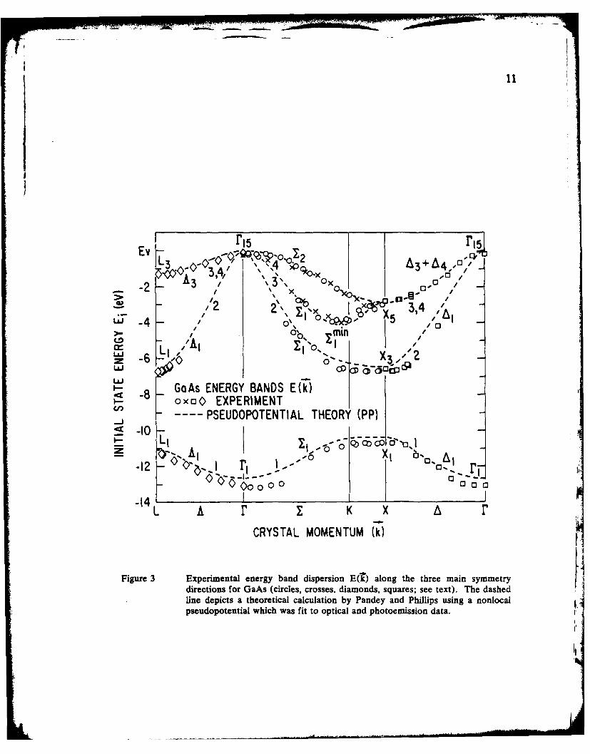
Experimental Energy vs. Momentum E(k) Band Dispersions for Solids: GaAs. We havedeveloped accurate new methods for directly determining the energy band dispersions E(1) ofa variety of materisls--emiconductors, metals, metallic compounds, etc., using angle-resolvedphotoemission with synchrotron radiation. Such measurements are of fundamental interest insolid state physics because a knowledge of one-electron energy bands is central to understand-ing many physical and chemical properties of materials. As an example of our many studies, abrief description of our determination of the E(C) dispersions of the prototype II-V semicon-ductor GaAs is given.
For semiconductors, despite numerous reported studies, only rather limited experimentalinformation about band dispersions has been obtained previously. In particular, GaAs, beingtechnologically important, has attracted much attention and is a model system for photoemis-sion studies. We have determined the experimental band dispersions E(f) of GaAs for thefirst time13 , 14 along all three major symmetry directions r-z-x, r-&-X and r-A-L. Ouraccomplishments have been two-fold: (i) to give a relatively more complete one-electrondescription for GaAs from experimental measurements, and (ii) to illustrate the usefulness andsuccess of such techniques which are of general utility for many materials.
Experimental band dispersions E(k) for GaAs have been determined along rzx, rAL,and rax and are summarized in Fig. 3 (circles, squares, crosses, and diamonds). Forcomparison, we show calculated dispersions (dashed lines) based on a nonlocal pseudopoten-tial model fit to optical and angle-integrated photoemission data. The theory agrees fairly wellfor GaAs (within -0.4 eV, worst case), which is the best understood III-V semiconductor. InFig. 3, E(T) dispersions along zx (circles) were determined using normal emission fromGaAs(l10) with photon energies in the 25 ~ h' 5 100 eV range. The same GaAs(l10)
!7
surface was used to determine E(C) dispersions along FAL (diamonds), raX (squares) andalong r x (crosses) using angular- and hy-dependent angle-resolved photoemissiontechniques.13 . 14 These techniques, which have been worked out for semiconductors for thefirst time, are of general utility and have been successfully applied to a number of selectedmaterials (see Summary Section).
I

REFERENCES
1. D.E. Eastman, J.J. Donelon, N.C. Hien, and FJ. Himpsel, An Ellipsoidal MirrorDisplay Analyzer System for Electron Energy and Angular Measurements, J. Nucl.Instrum. Methods, 1980, (in press).
2. J.E. Rowe and H. Ibach, Phys. Rev. Lett. 32, 421 (1974).
3. F. Jona, H.D. Shih, A. Ignatiev, D.W. Jepsen, and P.M. Marcus, J. Phys. CIO, L67
(1977).
4. M.J. Cardillo and G.F. Becker, Phys. Rev. Lett. 40, 1148 (1978).
5. R.E. Schlier and H.E. Farnsworth in Semiconductor Surface Physics (University ofPennsylvania Press, Philadelphia, 1957), pp. 3-22; J. Chem. Phys. 30, 917 (1959).
6. J.A. Appelbaum, G.A. Baraff, and D.R. Hamann, Phys. Rev. Lett. 35, 729 (1975).
7. G.P. Kerker, S.G. Louie, and M.L. Cohen, Phys. Rev. B17, 706 (1978).
8. L.A. Appelbaum, G.A. Baraff, and D.R. Hamann, Phys. Rev. B15, 706 (1978).
9. D.E. Eastman, F.J. Himpsel, J.A. Knapp, and K.C. Pandey, Proceedings of the 14thInternational Semiconductor Conference, Edinburgh, Scotland, September 1978.
10. T.D. Poppendick, T.C. Ngoc, and M.B. Webb, Surf. Sci. 75, 287 (1978).
11. J.A. Appelbaum and D.R. Hamann, Surf. Sci. 74, 21 (1978).
12. S.Y. Tong and A.L. Maldonado, Surf. Sci. 78, 459 (1978); M.A. Van Hove andK.A.R. Mitchell, Surf. Sci. (in press).
13. T.-C. Chiang, L.A. Knapp, and D.E. Eastman, Sol. St. Commun. 31, 917 (1979).
14. T.-C. Chiang and D.E. Eastman, Angle-Resolved Photoemission, Valence BandDispersions E(M), and Electron and Hole Lifetimes for GaAs, Phys. Rev. B, 1980 (inpress).
!' I
9
TWO-DIMENSIONAL ELECTRON SPECTROMETERCEMA PHOSPHORe7 LEED PLATES SCREEN S. T. 20 SRE- E
CAM MC MINI- 4015I
DETECTORR GRAPHIATED
LIGHT(IMNY
Figue 1 Schematic diagram (top view) of two-dimensional electron spectrometersystem. The retarding field ellipsoidal low pass filter, retarding field sphericalgrid high pass filter, and an area detector which consists of a CEMA multipierand phosphor screen are shown. Several detectors for angle-resolved PES,ange-integrated PES and Auger measurements are schematically shown,including a data acquisition system for recording digitally the entire screen.

10
Si (100) SURFACE-(2xl)
ENERGY(V)
GAP
EF= 0I 00. 00.l
THEORY EE
-I BULK
0 [oio]VELOCITY
(MOMENTUM)Figure 2 Energy band dispersion for surface states on Si(1O0)-(2x I) surface. The
theory curves (dotted) (Ref. 8) correspond to a metallic surface with surfacestates in the fundamental gap while we have experimentally determined thatthere are lower-lying surface states with a semiconducting surface.
11
r 15 r 15
L34, A3+A4,-,'
-2 - A3 ' , ox C3
.X C i
LiI -4 /do\E 1 ,X 3 /4 o
>- 0% o minl
(J) /Al 0 X 1°r L,: 11'0" 1
0 X3 .,
GaAs ENERGY BANDS E(k)-8 -
I.- oxO EXPERIMENT-j PSEUDOPOTENTIAL THEORY (PP)
LI 0-;06-12
I A1
L A r K X A r
CRYSTAL MOMENTUM W
Figure 3 Experimental energy band dispersion E(t) along the three main symmetrydirections for GaAs (circles, crosses, diamonds, squares; see text). The dashedline depicts a theoretical calculation by Pandey and Phillips using a nonlocalpseudopotential which was fit to optical and photoemission data.
]I

12
11. SUMMARY OF WORK COMPLETED UNDER CONTRACT
In the following, a brief summary is given of published research papers that were supported in
part by the Air Force Office of Scientific Research under contract F446720-70-C-0089. Forclarity, these research papers (34 in all) have been grouped into five sub-areas of research:
tA. Electronic structure of semiconductor surfaces and interfaces.B. Electronic structure of group IV and group I-V semiconductors.C. Electronic structure of metal surfaces.D. Electronic structure of metals and metallic compounds.E. Studies of electronic many-electron effects.
A. Electronic Structure of Semiconductor Surfaces and Interfaces.
1. Empty surface states on semiconductors: Their interactions with metal overlayers andtheir relation to Schottky barriers.
Measurements we have made of (EF-Ev) srace for n-type GaAs (110) indicatethat, contrary to some previous publications, there are no unoccupied surfacestates in the band gap of GaAs(110), i.e., (EF-Ev)sUfC is equal to the bandgap. This result has two major implications: (1) (EF-E v) sue is exceedinglysensitive to the quality of the cleavage, as well as to low exposures (<IL) ofresidual gases in UHV systems (even though gas sticking probabilities appearto be low); thus considerable care must be executed in using band bendingmeasurements as a probe of surface states. (2) Partial yield and electron-energy-loss measurements show transitions from core levels to unoccupiedsurface states at energies that, in the absence of excitonic shifts, would placethe one-electron energy of these unoccupied surface states on GaAs(110)- 0.5 eV below this observed position of EF. One must therefore concludethat these transitions involve strong excitonic binding, with an exciton bindingenergy EE, - 0.6 eV for GaAs(110). (W. Gudat, D. E. Eastman, and J. L.Freeouf, J. Vac. Sci. Technol. 13, 250 (1976).)
2. Electronic surface properties of HI-V semiconductors: Excitonic effects, band-bendingeffects, and interactions with Au and 0 adsorbate layers.
Photoemission studies of valence bands, core levels, empty surface states, andband bending for cleaved GaAs (110) are described. These studies show thatthere are no intrinsic band-gap surface states for GaAs (110), and that large(Z 0.5 eV) excitonic binding energies are involved in core-level-to-empty-surface-state transitions (e.g., using yield spectroscopy or electron energy-lossspectroscopy). Studies of the effects on chemisorbed oxygen and thin Auoverlayers on InAs (110) and GaAs (110) surfaces are also described. Trendsand correlations in III-V semiconductor empty surface states are discussed.(W. Gudat and D. E. Eastman, 1. Vac. Sci. Technol. 13, 831 (1976).)
3. Photoemission and band structure studies of the GaAs(1 10) Surface.
We have studied the electronic and geometrical structure of the cleavedGaAs(110) surface, using experimental ultraviolet photoemission spectroscopy
. , ml[ .... " ....... .MI A

13
(UPS) of both filled and empty surface states together with tight-bindingcalculations. We have considered several different types of structural models,including the relaxation model in which surface Ga atoms move into, and Asatoms move out of, the surface by an amount such that the plane through thenearest neighbor Ga and As atoms makes a tilt angle, OT , with the corre-sponding plane in the ideal surface while bond lengths remain constant. Weshow that this model with a tilt angle OT - 190 - in contrast with OT - 350as previously concluded from a LEED (low energy electron diffraction)analysis - adequately accounts for the photoemission spectroscopy data. Adescription of the nature of surface states including the local s- and p-orbitaldensities of states and dispersion relations is given for this relaxation model.(K. C. Pandey, J. L. Freeouf, and D. E. Eastman, J. Vac. Sci. Technol. 14,904 (1977).)
4. Chemisorption of chlorine on Si( 11l) 7 x 7 and 1 x 1 surfaces.
Using ultraviolet photoemission spectroscopy (UPS) in conjunction withtheoretical calculations, we have studied the reaction of gaseous chlorine withSi( 111) 7 x 7 and 1 x I surfaces. The UPS spectra of the two chlorine saturat-ed surfaces are very similar and consist of four peaks, a sharp main peak at-10.7 eV and smaller ones at -7.5, -13.0, and -15.7 eV relative to thevacuum level. Both the peak positions and their relative intensities are inquantitative agreement with a theoretical calculation for a structural model inwhich a single chlorine atom sits on top of each surface Si atom, indicatingthat C1 2 decomposes at the surface to make strong covalent bonds with Si.(K.C. Pandey, T. Sakurai, and H.D. Hagstrom, Phys. Rev. B16, 3648 (1977).)
5. Reaction of atomic hydrogen with Si( 111) surfaces: formation of monohydride andtrihydride phases.
By using a realistic tight-binding or LCAO (linear combination of atomicorbitals) model, detailed calculations of surface states, local densities of states,and theoretically simulated photoemission spectra have been carried out fortwo qualitatively distinct structural models for chemisorption of atomic hydro-gen on Si(l 11)1 x I surfaces. In the low-coverage model, called the monohy-dride phase or Si( I1l):H, it is assumed that a single hydrogen atom sits on topof each surface Si atom, thus saturating all dangling bonds. In the high-coverage model, designated as the trihydride phase or Si(Il1):SiH3, SiH 3radicals are bonded to the surface Si atoms. Due to the radically differentatomic structures, the theoretical spectra of the two phases show strikingdifferences. A comparison of the theoretical spectra with the ultravioletphotoemission spectra taken during hydrogen chemisorption on the quenchedSi(lll)lxl surface clearly shows that at low coverages the monohydride isformed, while at high coverages the trihydride phase is formed. Formation ofthe monohydride phase is expected on simple chemical and structural consider-ations, and it has been observed on other Si surfaces. However, formation ofthe trihydride phase is unique to Si(111)1 x 1 and as such, it has importantimplications regarding the structure and stability of clean Si(l 11) 1 x 1. (K. C.Pandey, IBM Journal of Research and Development, 22, 250 (1978).)
6. Atomic and electronic structure of semiconductor surfaces
The electronic structure of surfaces, which can be determined by variouselectron/ion spectroscopies including ultraviolet photoemission spectroscopy

14
(UPS), is dependent on the surface atomic geometry. Thus, it is possible todetermine the surface atomic structure via structure-dependent theoreticalanalyses of these experimental spectra. Because of the complexity of suchsystems, a simple but accurate theoretical scheme is required. We show thatthe valence electronic states and atomic structures of semiconductorsurfaces-both clean and with chemisorbed species as well as relaxed and/orreconstructed-can be determined using a tight-binding model. Such calcula-tions together with UPS data show that the annealed Si( 111)7x7 surfacecontains about 25% vacancies. For GaAs(110), we have found that the Gaatoms move into, and As atoms move out of the surface with small bondlength distortions so that a plane through them makes an angle of about 200with the surface. We show that H chemisorbed on Si(111) has two distinctstructural phases: a monohydride phase at low coverages, and a rather unex-pected trihydride phase at high coverages. (K. C. Pandey, Physics ofSr, 1978, Inst. of Phys. Conf. Series 43, Bristol and London,1051 (1979)).
7. Atomic and electronic structure of Si(l 11)7 x 7 surface.
Calculations of the surface electronic structure of the Si(111)7x7 surface forseveral different structural models have been carried out. Two structuralmodels, a vacancy model and a buckled surface model, give surface electronicstructures consistent with angle-averaged photoemission spectra. However, theorigin and symmetry of surface states in the two models are different. Wepoint out that these differences, in conjunction with further experiments, canbe used to decide between the two models. (K. C. Pandey, Physics of Semi-conductors 1978, Inst. of Phys. Conf. Series 43, Bristol and London, 1051(1979).)
8. Surface electronic structure studies of GaAs( 110).
Angle-resolved photoemission using synchrotron radiation from GaAs(110)has been studied in conjunction with tight binding calculations of the surfaceelectronic structure. Emission from two new surface resonances-which werepredicted to exist only for a relaxed surface-have been identified near theedges of the surface Brillouin zone at X and X'. Also, measurements of thedispersion of the As-derived surface state near the valence band maximum,first reported elsewhere, have been extended from r to the zone edge X and aband width of 0.6 eV has been determined. All of these observations, includ-ing those reported elsewhere of intrinsic surface states on GaAs(110) areaccounted for by a tight binding model calculation for a relaxed surface( 190 bond angle rotation). (J. A. Knapp, D. E. Eastman, K. C. Pandey,and F. Patella, J. Vac. Sci. Technol. 15, 1252 (1978).)
9. Angle-resolved photoemission studies of semiconductor bulk and surface states.
Polarization-dependent angle-resolved photoemission studies using synchrotronradiation together with theoretical models permit both energy and momentuminformation (e.g., E (E) dispersions) to be obtained for semiconductor bulkand surface states. Illustrative applications for intrinsic surface states(Si(l1l)-(7x7)), adsorbate states (Si(1l1):H), and bulk electronic states(GaAs(l10)) are described. (D. E. Eastman, F. J. Himpsel, J. A. Knapp andK. C. Pandey, Phfics of Sai moru 1975, Inst. of Phys. Conf. Series 43,Bristol and London, 1059 (1979).)

15
10. Quantum photoyield of diamond( 11) - a stable negative affinity emitter.
Quantum photoyield and secondary electron distributions have been measuredfor an unreconstructed diamond(l 11) surface (type Hlb, gem quality blue-whitesemiconductor). This chemically inert surface exhibits a negative electron
affinity, resulting in a stable quantum yield that increases linearly from pho-tothreshold (5.5 eV) to - 20% at 9 eV, with a very large yield of - 40-70%
for 13 S h, _< 35 eV. For all photo energies, secondary electron energydistributions show a dominant - 0.5 eV wide emission peak at the conductionband minimum (Amin-5.50±0.05 eV above the valence band maximum r 25').In contrast with recent self-consistent calculations (J. Ihm, S.G. Louie, andM.L. Cohen, Phys. Rev. B17, 769 (1978)), no occupied intrinsic surfacestates with ionization energies in the fundamental gap (the Fermi level was1 eV above r'25') were observed. Likewise, the measured photothreshold(EVa-F25') is significantly smaller than calculated (7.0±0.7 eV). (F. J.Himpsel, J. A. Knapp, J. A. VanVechten and D. E. Eastman, Phys. Rev. B20,624 (1979).)
11. Photoemission studies of intrinsic surface states on Si(100).
We have determined the energy vs k, dispersion of intrinsic surface states onSi(100) (2 x 1) by means of angle-resolved photoemission with synchrotronradiation. For k1 -0, there is a very pronounced surface state 0.7 eV belowEFi.e., - 0.4 eV below the top of the valence band) which disperses down-wards with increasing k1 . At J' on the boundary of the surface Brillouin zone,we find two states with binding energies of 0.7 and 1.2 eV with respect to EF.A rumber of geometrical models and their corresponding theoretical surfacestate bands have recently been published for Si(100)(2xl). Our resultsdisagree qualitatively with all surface state dispersions calculated to date, i.e.,the ideal surface, the vacancy model, the pairing model, and the zig-zag-chainmodel. Namely, we observed semiconducting surface state bands with a lowstate density at EF while all models calculated to date yield metallic surfacestates with a large state density at EF. (F. J. Himpsel .-nd D. E. Eastman, J.Vac. Soc. Technol. 16, 1297 (1979).)
12. Microscopic compound formation at the Pd-Si( 111) interface.
Photoemission studies of Pd on clean Si(lll) surfaces show that formation ofthe Pd 2Si compound dominates the microscopic chemistry and properties ofthe Pd-Si interface. No evidence is found for interface dipoles or occupiedmetal-induced interface states in this system. The Pd2 Si reaction product (ametal) has an electronic structure more like that of the noble metals than thetransition metals, with an occupied 4d band located - 2.75 eV below theFermi energy. (J.L. Freeouf, G.W. Rubloff, P.S. Ho, and T.S. Kuan, Phys.Rev. Lett. 43, 1836 (1979).)
13. Silicide Schottky barriers: an elemental description.'
A model for reactive Schottky barrier formation has been proposed andapplied to silicide contacts on silicon. Approximate workfunctions calculatedassuming a silicon excess near the silicide/silicon interface reconcile measuredbarrier heights with a simple Schottky description of their energetics.(J.L. Freeouf, Sol. St. Commun. 33, 1059 (1980).)

16
14. Geometrical and electronic structure of Si(001) and Si(l 11) surfaces: a status report.
A critical review of recent studies of the geometrical and electronic structureof the Si(001) and Si( 11) surfaces has been made. Emphasis is placed onlow-energy electron diffraction (LEED) studies of the geometrical structure,photoelectron spectroscopy studies of the electronic structure, and theoreticalstudies of the electronic and geometric structure of the Si(ll)-(2x 1),Si( 11 )-(7 x 7), Si( I1 )-(1 x 1), and Si(001)-(2 xl) surfaces. (D.E. Eastman,J. Vac. Si. Technol. (in press).)
B. Electronic Structure of Group IV And Group I-V Semiconductors
15. Photoemission spectroscopy using synchrotron radiation. H. The electronic structureof germanium.
We analyze photoemission spectra for Ge obtained for photon energies 6.5 Shr S 25 eV and determine the position of energy bands at symmetry pointsfor both filled and empty bands within 1 Ry of the gap. This experimentalband structure is obtained using a recently developed anisotropic direct-transition model of photoemission applicable to cleaved single-crystal semicon-ductors. For the band-structure determination we also employ a direct trans-ition analysis of optical spectra obtained by others. We fit nonlocal-pseudopotential calculations to the experimentally-determined band positions,and thereby determine the importance of both energy and I = 2, angularmomentum nonlocality in the pseudopotential. Our results for the position ofhigh-lying conduction-band states suggest 0 to + 10% self-energy (exchange-correlation) corrections to the energy of electrons excited into the conductionbands. Energy bands which provide a good fit to the experimental bandpositions are used, along with pseudo-wave-function matrix elements, tocalculate various physical properties (photoemission spectra, optical-responsefunctions, and one-electron state densities), and the results of these calcula-tions are compared with experiment. The quality of the fits obtained indicatesthat the electronic excited-state (and ground-state) properties of Ge forexcitations far from the gap are described well by a one-electron model. (W.D. Grobman, D. E. Eastman, and J. L. Freeouf, Phys. Rev. B12, 4405(1975).)
16. Angle-resolved photoemission and valence band dispersions E(I) for GaAs: Direct vs.Indirect Models.
Angle-resolved photoemission measurements for GaAs( 110) have been extend-ed to hi-100 eV. These results show that dominant emission peaks are dueto direct transitions. Weaker one-dimensional density of states featuressometimes observed are due to surface umklapp/secondary cone and lifetimeeffects. Accurate band dispersions E() for al four valence bands of GaAsalong the [1101 direction are given using simple normal emission and off-normal emission methods. Electron and hole lifetimes are directly determined.(T.-Chiang, J.A. Knapp, and D.E. Eastman, Sol. St. Commun. 31, 917 (1979).
17. Angle-resolved photoemission and valence band dispersions E(t) and electron andhole lifetimes for GaAs.
Accurate valence band dispersions E(C ) along the major symmetry directionsr-i-X, r-A-X, nd r-A-L have been determined for GaAs using simple angle-

17
resolved photoemission techniques of general utility with synchrotron radiationfor 25 5 hi S 100 eV. At these photon energies, emission features can beunderstood within the direct transition model and spectral peaks can beclassified roughly into two categories: one being those associated with primarycone emission with a lifetime broadened free-electron-like final state disper-sion, and the other (usually weaker) being those associated with secondarycone/surface umklapp emission which emphasizes valence band critical pointswith high state densities. Valence band dispersions E(f) along the r-K-Xsymmetry line perpendicular to the surface are determined using normalemission spectra (primary cone peaks) from the (110) surface at variousphoton energie. Valence band dispersions E() along r-K-X, F-A-X, andr-A-L symmetry lines parallel to the surface are determined using off-normalemission spectra (primary cone peaks) from the same (110) surface with fixedperpendicular component of the electron momentum hk± at the zone center(extended zQse scheme) and varying parallel component of the electronmomentum AkI , which are obtained by suitably varying hi and emissionangles. Experimental valence band dispersions and critical points are com-pared with other theoretical and experimental results. Simple formulae arederived to relate the widths of spectral peaks to electron and hole lifetimes.Initial hole lifetimes at valence critical points and typical final electron life-times are obtained. The latter yields final state momentum broadening(typically : 10% of the Brillouin zone size) which are consistent with thedirect transition model. (T.-C. Chiang and D.E. Eastman, Phys. Rev. (inpress).)
18. Experimental energy band dispersions, critical points, and spin-orbit splittings forGaSb using angle-resolved photoemission.
We have determined energy band dispersions E(t) and critical points for GaSbusing angle-resolved photoemission techniques. With a normal emissionconfiguration and photon energies between 24 and 95 eV, the valence banddispersions E(T) have been obtained along the r-K-X direction, with thespin-orbit splitting Ao(ra-r 7) clearly observed. With an off-normal emissionconfiguration, we have also determined the valence band critical point energiesat the L point, with the spin-orbit splitting A1(L4 ,3 -L6 ) clearly observed.Experimental valence band critical point energies at r, X and L are comparedwith recent theoretical results. Using published transition energies determinedfrom reflectance measurements, we have also obtained the low-lying conduc-tion band critical point energies. These valence and conduction band criticalpoint energies are tabulated to facilitate comparisons with other experimentaland theoretical results. (T.-C. Chiang and D.E. Eastman, Phys. Rev. (inpress).)
.1
C. Electronic Structure of Metal Surfaces.
19. Observation of a A I-Symmetry Surface State on Ni( 111).
An s-p-like intrinsic surface state on Ni(l I I) has been found which has anenergy of Ei - -0.25 eV relative to the Fermi energy at f and lies betweenthe L3 (El a -0.15 eV and L2' (Ei - -0.9 eV) bulk states. Its momentumdispersion (E vs I) and h-dependent photoionization cross section have been '
1s
determined using angle-resolved photoemission with synchrotron radiation.The existence of this state significantly affects spin-polarized photoemission,chemisorption, band-structure, and exchange-splitting interpretations for Ni.(F.J. Himpsel and D.E. Eastman, Phys. Rev. Lett. 41, 507 (1978).)
20. Intrinsic A,-symmetry surface state on Co(0001).
An intrinsic surface state on Co(0001) has been found using angle-resolvedphotoemission with synchrotron radiation which has an energy of Ei - -0.3 eVat r (zone center) relative to the Fermi energy EF . Its symmetry has beendetermined to be of A1 character using measurements with s- and p-polarizedradiation. Its momentum dispersion (E vs 1 ) and h,-dependent photoioniza-
tion cross section have also been determined. At the zone center f, thesurface state lies in an absolute energy gap just above the uppermost A3d-like (Ei - -0.35 eV) bulk state, well above the uppermost sp-like, A, state(El= -1.15 eV), and below occupied A34 d-like bulk states near r (energiesbetween _, = -0.05 eV and 0). As previously reported for Ni, this surfacestate is extremely sensitive to absorbates and significantly affects field emis-sion, spin-polarized photoemission, chemisorption, etc. for Co(0001). (F.J.Himpsel and D.E. Eastman, Phys. Rev. B20, 3217 (1979).)
D. Electronic Structure of Metals and Metallic Compounds.
21. Electronic structure of the thorium hydrides ThH2 and Th4 H1 5 .
Photoelectron spectroscopy using synchrotron radiation has been used to studythe electronic structure of single-phase stoichiometric ThH2 and Th 4H1 S.Th-derived conduction bands are observed together with lower-lying hybri-dized bonding bands. For Th4 S, a narrow d-like conduction band(- 0.6-eV full width at half-maximum) separated from other bands by a 2-eVband gap is seen. Energy-dependent cross-section measurements for thevarious bands have been used to determine hybridization and angular momen-tum character. (J.H. Weaver, J.A. Knapp, D.E. Eastman, D.T. Peterson, andC.B. Satterwaite, Phys. Rev. Lett. 39, 639 (1977).)
22. Experimental band structure and temperature-dependent magnetic exchange splittingof nickel using angle-resolved photoemission.
Using angle-resolved photoemission and synchrotron radiation, we havedetermined the energy-versus-momentum valence-band dispersion relations fora Ni( 111) crystal. The temperature-dependent ferromagnetic exchange split-ting has been directly observed. Both the d-band width (-3.4 eV at L) andexchange splitting (0.31 eV) are much smaller than theoretical estimates(-4.5 eV wide at L with -0.7-eV splitting, respectively, at 293 K. (D.E.Eastman and F.J. Himpsel, Phys. Rev. Lett. 40, 1514 (1978).)
23. Direct determination of lifetime and energy dispersion for the empty A, conductionband of copper.
We present an accurate determination of the energy dispersion (E vs k) andthe first direct determination of the energy-dependent lifetime F(E) of well-defined excited Bloch states in a crystal. Using angle-resolved photoemissionfor Cu(100), we find that the lifetime broadening increases from r - 1.2 eV(6x 10"16 sec) for A, conduction-band states ranging 10.5 to 13.5 eV above

19
the Fermi level. The measured dispersion (-2% accuracy) shows a reducedeffective mass (m/m 0 -0.90--0.94) which is related to self-energy effects.(D.E. Eastman, $.A. Knapp, and F.J. Himpsel, Phys. Rev. Lett. 41, 825(1978).)
24. Experimental energy dispersions for valence and conduction bands of palladium.
Using angle-resolved photoemission with synchrotron radiation, we havedetermined accurate energy-versus-momentum dispersion relations along the<111 direction using a Pd(lll) crystal. The energy E (:5 0.1 eV accuracy)and the momentum parallel to the surface Tl are measured directly. Theperpendicular component of the momentum k. is obtained from the measuredfinal energy via a calculated free-electron-like final band that is found to beaccurate within ±5% of the zone-boundary momentum by comparison withcertain critical points that have been measured directly (LI, r" 2, and r 15 ). Forthe initial bands, we find the dispersions of the two d-like A3 bands and of thesp-type A, band. Measured critical points (in eV) for bands numbered withincreasing energy are: r2,3,4 - -2.55 ± 0.15, r,, 6 - -1.15 ± 0.I, r 7 - 18.4t 0.5, r. - 21.7 ± 0.5, L4 = -0.4 ± 0.2, LS -0.1 ± 0.1, and L7 = 7.7 ± 0.3.Spin-orbit splitting (-0.4 eV maximum) is observed for the upper A3 band.(F.J. Himpsel and D.E. Eastman, Phys. Rev. B18, 5236 (1978).)
25. Experimental energy-band dispersions and exchange splitting for Ni.
Angle-resolved polarization-dependent photoelectron spectroscopy usingsynchrotron radiation has been used to determine the energy-versus-momentum band dispersions and magnetic exchange splitting of Ni. UsingNi( 11) and Ni(100) crystals, the band dispersions along the F-L and r-xlines have been determined for the s and d bands. The temperature-dependentmagnetic exchange splitting AE., of the upper A3 band has been directlyobserved and found to be independent of momentum k for a large region ofthe Brilouin zone. The experimental value of AE., - 0.31 ± 0.03 eV issmaller than recent calculated values (0.6 g AE01 < 0.9 eV) obtained withspin-polarized self-consistent band calculations. Also, calculated d-bandwidths are larger (typically 40%) than measured (3.4 eV at L). Our resultsare consistent with Fermi-surface data and the polarization reversal observedin spin-polarized photoemission. A number of previous contradictory pho-toemission studies of Ni are discussed in view of our results. The observedbands show that ferromagnetic nickel can be described by a Stoner-Wohlfarth-Slater spin-split band model. (F.J. Himpsel, J.A. Knapp, and D.E. Eastman,Phys. Rev. B19, 2919 (1979).)
26. Experimental energy band dispersions and lifetimes for valence and conduction bandsof copper using angle-resolved photoemission.
Energy band dispersions and electron lifetimes have been determined for bothvalence and conduction band states of copper using angle-resolved photoemis-sion with polarized synchrotron radiation in the 5 5 hr S 35 eV photonenergy range. Dispersion relations for the occupied s-p and 3d bands of Cualong the r-X and r-L symmetry lines (including critical points at r, X, and
) have been determined with an accuracy of 0.05-0.1 eV and < 5% of thezone boundary momentum. Band symmetries have been deduced using polari-zation selection rules. The dispersion relation has also been accurately deter-mined for the unoccupied &I conduction band along r-X at -10-15 eV above

21
the Fermi energy EF ; this band has a reduced effective mass (m=.90-.94)which is related to self-energy effects. Lifetimes have been directly measuredfor excited hole states (the lifetime broadening rh increases from -0.2 to0.5 eV FWHM for d-band energies from 2 to 5 eV below EF) as well as forexcited electron states in the A, conduction band (rob 1.0 to 2.0 eV forenergies 10 to 15 eV above EF). The energy dispersion and h-dependentphotoionization cross section of the s-p surface state on Cu( 11) are reported.Previous theoretical and experimental studies of copper are compared with ouraccurate E vs. It dispersions. (J.A. Knapp, F.J. Himpsel, and D.E. Eastman,Phys. Rev. B19, 4952 (1979).)
27. Temperature dependence of bulk and surface energy bands in copper using angle-resolved photoemission.
We have directly measured thermally induced changes in surface and bulkenergy-band dispersions of copper by examining angle-resolved photoemissionfrom Cu(lll) and Cu(100) surfaces for temperatures from 25 to 5000C.Polarized synchrotron radiation was used as the photon source. Observedshifts in the bulk band structure are in reasonable agreement with energy shiftscalculated for the corresponding temperature-dependent lattice changes. Themeasured temperature coefficient for the upper d band along A is1.5(±0.1)x10"4 eV/K, while the lower edge of the d bands shifts by2.0(±0.2)xiO4 eV/K. The d-band width decreases with temperature at arate of 0.5(±0.2)x10"4 eV/K as it shifts to higher energy. The Cu(1ll)surface state shifts toward EF with a measured temperature coefficient of2.7(±0.1)xi0" 4 eV/K. (.A. Knapp, F.J. Himpsel, A.R. Williams, and D.E.Eastman, Phys. Rev. 019, 2844 (1979).)
28. Symmetry method for the absolute determination of energy-band dispersions E)using angle-resolved photoelectron spectroscopy.
Angie-resolved spectra for emission in a mirror plane as a function of emissionang. and photon energy hi show critical-point behavior in interband intensi-ties for transitions on zone boundaries. For such transitions, the absoluteenergies E and crystal momentum If for both the initial and final states aregiven by hi and the emission angle. E(IE) dispersions have been determinedfor several d bands and conduction bands along the 4, A, and e axes ofcopper. (Eberhard Dietz and D.E. Eastman, Phys. Rev. Lett 41, 1674(1978).)
29. Experimental band dispersions E() along three main symmetry lines of LaB6 usingangle-resolved photoemission from one crystal surface.
Accurate valence band dispersions EM') of LaB6 have been determined alongthree main symmetry lines rM, rx, and XM using one single crystal (001)surface by a simple new photoemision technique of general utility. Usingdirect interband transitions, E(M) dispersions are mapped out by suitablyscanning polar emission angie and the photon energy. Detailed results agreewell with recent X,-APW energy band calculations. (M. Aono, T.-C. Chiang,J.A. Knapp, T. Tanaka, and D.E. Eastman, Sol. St. Commun. 32, 271(1979).)

30. Experimental exchange-split energy band dispersions for Fe and Co.
Using angle-resolved photoemission with single crystal Fe(l 11) and Co(000 1)we have determined accurate exchange-split energy band dispersions E()along symmetry lines. For Fe, Co, and Ni, respectively, occupied d-bandwidths are 3.1 eV (P), 3.8 eV (L) and 3.4 eV (L,X) while exchange splittingsare -1.5 eV (P), -1.1 eV (r) and 0.3 eV (near L). Comparison with theoryshows that state-of-the-art ab-initio calculations describe the strong ferromag-nets Fe and Co much better than Ni. (D.E. Eastman, F.J. Himpsel and J.A.Knapp, Phys. Rev. Lett. 44, 95 (1980).)
31. Experimental energy band dispersions and magnetic exchange splitting for cobalt.
We have determined E vs. I energy band dispersions of cobalt for s- andd-bands along the hexagonal axis FAA ([0001]-direction) via angle resolvedphotoelectron spectroscopy from a Co(0001)-face using synchrotron radiation.We obtain the magnetic exchange splitting at r for the upper d-band(0.85±0.2 eV) and lower d-band (1.2±0.3 eV). The overall occupied d-bandwidth (-3.8 eV at L) is about 20% narrower than a state-of-the-art self-consistent band calculation using a local density theory of exchange-correlation. The top of the majority spin d-bands is 0.35 eV below EF . Thereis a small r-centered minority electron pocket at EF which explains previouslyunidentified deHaas van Alphen orbits. We present dipole selection rules forthe A axis of a hcp lattice and show that the number of allowed transitions isreduced drastically for emission along the A-axis. The allowed transitions canbe interpreted in the same way as those for emission normal to a (111 ) face ofa fcc lattice. (F.J. Himpsel and D.E. Eastman, Phys. Rev. (in press).)
E. Studies of Electronic Many-Electron Effects..
32. Resonant photoemission shake-up and Auger processes at the 3p photothreshold in Gaand GaP.
Resonant photoemission 3d8 shake-up satellites in Ga metal and GaP, whichare closely related to M2,3M4 ,5 M4 ,5 Auger transitions, have been observed atthe 3p phototbreshold of Ga. By analyzing the line positions, multipletstructure, and resonant behavior near threshold, we have determined theexcitonic binding energies and correlation energies for various one-hole andtwo-hole excited states. While these two-hole excitations in Ga metal andGaP are similar because of their quasi-atomic nature, important differences areobserved which are due to different final state screening mechanisms for ametal and an insulator. The present results are compared with those for Cuand Ni. (T.-C. Chiang and D.E. Eastman, Phys. Rev. (in press).
33. Observation of the transition from the adiabatic to the sudden regime for theM3 M4,SM4 ,5 (G) Auger excitation in zinc.
We have observed that the photoexcited M3M4 ,5 M4 ,5 (IG) Auger line in Znasymmetrically broadens to lower energy with increasing photon energy. Thebroadening can be described by a change in the asymmetry parameter&a=0.09 using a Doniach-Sunjic lineshape. This is the first evidence for the

22
transition from the adiabatic to the sudden regime in a solid. The onset of thischange - 14 eV above threshold is related to 3d screening electron excita-tions which are seen as 3p core level satellites. (F.J. Himpsel, D.E. Eastman,and E.E. Koch, Phys. Rev. Lett. 44, 214 (1980).)
34. Two-electron resonances at the 3p-threshold of Cu and Ni.
A sharp 3d-electron satellite excitation has been found for Cu which exhibits astrong resonant enhancement (-x5) at the Cu 3p core level threshold similarto the 6 eV resomnant satellite observed previously in Ni. This satellite, whichhas two peaks at 11.8 and 14.6 eV below EF, is identified as a quasi-atomictwo-electron excitation with two 3d-holes plus one 4s electron (3d4s). Pres-ent models for the Ni resonant satellite are not able to describe our Cu results.(M. Iwan, F.J. Himpsel, and D.E. Eastman, Phys. Rev. Lett. 43, 1829(1979).)

23
III. LIST OF PUBLICATIONS UNDER CONTRACT
A. Electronic structure of semiconductor surfaces and interfaces.
I. Empty Surface States on Semiconductors: Their Interactions with Metal Overlayersand Their Relation to Schottky Barriers, W. Gadat, D.E. Eastman and J.L. Freeouf, J.Vac. Sci. Technol. 13, 250 (1976).
2. Electronic Surface Properties of Ill-V Semiconductors: Excitonic Effects, BandBending Effects, and Interactions with Au and 0 Adsorbate Layers, W. Gudat andD.E. Eastman, J. Vac. Sci. Technol 13, 831 (1976).
3. Photoemission and Band-Structure Studies of the GaAs(l10) Surface, K.C. Pandey,J.L. Freeouf and D.E. Eastman, J. Vac. Sci. Technol. 14, 904 (1977).
4. Chemisorption of Chlorine on Si(Ill) 7x7 and IxI Surfaces, K.C. Pandey, T.Sakurai, and H.D. Hagstrom, Phys. Rev. B16, 3648 (1977).
5. Reaction of Atomic Hydrogen with Si(1 11) Surfaces: Formation of Monohydride andTrihydride Phases, K.C. Pandey, IBM J. Res. Develop. 22, 250 (1977).
6. Atomic and Electronic Structure of Semiconductor Surfaces, K.C. Pandey, J. Vac. Sci.Technol. 15, 440 (1978).
7. Atomic and Electronic Structure of Si(111)7x7 Surface, K.C. Pandey, Physics of, oaicdm 1975 Inst. of Phys. Conf. Series 43, Bristol and London, 1051 (1979).
8. Surface Electronic Structure Studies of GaAs(110), JA. Knapp, D.E. Eastman, K.C.Pandey and F. Patella, J. Vac. Sci. Technol. 15, 1252 (1978).
9. Angle-Resolved Photoemission Studies of Semiconductor Bulk and Surface States,D.E. Eastman, F.J. Himpsel, JA. Knapp and K.C. Pandey, Physles of Sami ors1978, Inst. of Phys. Conf. Series 43, Bristol and London, 1059 (1979).
10. Quantum Photoyield of Diamond(I 11) - A Stable Negative Affinity Emitter, F.J.Himpsel, I.A. Knapp, J.A. VanVechten and D.E. Eastman, Phys. Rev. 20, 624 (1979).
11. Photoemission Studies of Intrinsic Surface States on Si(100), F.J. Himpsel and D.E.Eastman, J. Vac. Soc. Technol. 16, 1297 (1979).
12. Microscopic Compound Formation at the Pd/Si(111) Interface, J.L. Freeouf, G.W.
Rubloff, P.S. Ho and T.S. Kuan, Phys. Rev. Lett. 43, 1836 (1979).
13. Silicide Schottky Barriers: An Elemental Description, J.L. Freeouf, Sol. St.Commun.33, 1059 (1980).
14. Geometrical and Electronic Structure of Si(001) and Si(ll1) Surfaces: A Status Ij
Report, D.E. Eastman, J. Vac. Sci. Technol. (in press).

24
B. Electronic structure of Group IV and Group III-V semiconductors.
15. Photoemission Spectroscopy Using Synchrotron Radiation. II The Electronic Structureof Germanium, W. D. Grobman, D. E. Eastman, and J. L. Freeouf, Phys. Rev. B12,4405 (1975).
16. Angle-Resolved Photoemission and Valence Band Dispersion E () for GaAs: Directvs Indirect Models, T-C. Chiang, J.A. Knapp and D.E. Eastman, Sol. St. Commun. 31,917 (1979).
17. Angle-Resolved Photoemission, Valence Band Dispersions E(M), and Electron andHole Lifetimes for GaAs, T.-C. Chiang, J.A. Knapp, M. Aono, and D.E. Eastman,Phys. Rev. (in press).
18. Experimental Energy Band Dispersions, Critical Points, and Spin-Orbit Splittings for
GaSb Using Angle-Resolved Photoemission, T.-C. Chiang and D.E. Eastman, Phys.Rev. (in press).
C. Electronic structure of metal surfaces.
19. Observation of a A,-symmetry Surface State on Ni(lll), F. J. Himpsel and D. E.Eastman, Phys. Rev. Letters 41, 507 (1978).
20. An Intrinsic Ai-Symmetry Surface State on Co(0001), F. J. Himpsel and D. E.Eastman, Phys. Rev. B20, 3217 (1979).
D. Electronic structure of metals and metallic compounds.
21. Electronic Structure of the Thorium Hydrides ThH2 and Th4 H1 5 , J. H. Weaver, J. A.Knapp, D. E. Eastman, D. T. Peterson, and C. B. Satterhwaite, Phys. Rev. Letters 39,639 (1977).
22. Experimental Band Structure and Temperature-Dependent Magnetic ExchangeSplitting of Nickel Using Angle-Resolved Photoemission, D. E. Eastman and F. J.Himpsel, Phys. Rev. Letters 40, 1514 (1978).
23. Direct Determination of Lifetime and Energy Dispersion for the Empty AI ConductionD. E. Eastman, J. A. Knapp and F. J. Himpsel, Band of Copper, Phys. Rev. Lett., 41,825 (1978).
24. Experimental Energy Dispersion for Valence and Conduction Bands of Palladium, F. J.Himpsel and D. E. Eastman, Phys. Rev. BIi, 5236 (1978).
25. Experimental Energy Band Dispersions and Exchange Splitting for Nickel, F. J.Himpsel, J. A. Knapp and D. E. Eastman, Phys. Rev. B19, 2919 (1979).
26. Experimental Energy Band Dispersions and Lifetimes for Valence and ConductionBands of Copper using Angle-Resolved Photoemission, J. A. Knapp, F. J. Himpsel andD. E. Eastman, Phys. Rev. B19, 4952 (1979).
27. Temperature-Dependent Energy Band Dispersion of Surface and Bulk Bands ofCopper using Angle-Resolved Photoemission, J. A. Knapp, F. J. Himpsel, A. R.Williams and D. E. Eastman, Phys. Rev. B19, 2844 (1979).

25
28. Symmetry Method for the Absolute Determination of Energy Band Dispersion E(r)using Angle-Resolved Photoelectron Spectroscopy, Eberhard Dietz and D. E. EastmanPhys. Rev. Letters 41, 1674 (1978).
29. Experimental Band Dispersions E () Along Three Main Symmetry Lines of LaB6Using Angle-Resolved Photoemission from a One Crystal Surface, M. Aono, T-C.Chiang, J.A. Knapp, T. Tanaka and D.E. Eastman, Sol. St. Commun. 32, 271 (1979).
31. Experimental Exchange-Split Energy Band Dispersions for Fe and Co, D.E. Eastman,F.J. Himpsel and J.A. Knapp, Phys. Rev. Lett. 44, 95 (1980).
32. Experimental Energy Band Dispersions and Magnetic Exchange Splitting for Cobalt,F.J. Himpsel and D.E. Eastman, Phys. Rev. (in press).
E. Studies of electronic many-electron effects.
32. Two-Electron Resonance at the 3p-Threshold of Cu and Ni, M. Iwan, F.J. Himpseland D.E. Eastman, Phys. Rev. Lett. 43, 1829 (1979).
33. Observation of the Transition from the Adiabatic to the Sudden Regime for theM3 M4,SM4 ,5 (IG) Auger Excitation in Zinc, F.J. Himpsel, D.E. Eastman, and E.E.Koch, Phys. Rev. Lett. 44, 214 (1980).
34. Resonant Photoemission Shake-Up and Auger Processes at the 3p Photothreshold inGa and GaP, T.-C. Chiang and D.E. Eastman, Phys. Rev. (in press).

26
IV. BIOGRAPHY OF PRINCIPAL INVESTIGATOR
BIOGRAPHY:
Dean E. Eastman received his BS, MS and Ph. D. degrees in Electrical Engineering atM.I.T. in 1962, 1963, and 1965, respectively. He has held a National Merit Scholarship (1958to 1962), National Science Foundation Cooperative Fellowship (1962-1963) and IBMFellowship (1963-65). He is an IBM Fellow, and is also the manager of the Photoemissionand Surface Physics Group at IBM. Currently he is Chairman of the Solid State SciencesCommittee of the National Academy of Sciences, a Fellow of the American Physical Society, amember of the Users Executive Committee of the Synchrotron Radiation Center at the.University of Wisconsin, a member of the National Science Foundation Advisory Committeefor Condensed Matter Science, and a member of the Advisory Committee for the NationalSynchrotron Light Source Project, Brookhaven National Laboratory. He was a visitingProfessor of Electrical Engineering at M.I.T. (1972-13 academic year). He is the co-recipientof the 1980 Buckley Prize of the American Physical Society. His interests include developingnew photoemission spectroscopy techniques and applying them to a broad range of studies ofthe electronic band structure of solids and surfaces, chemisorption and semiconductor interfac-es.

27
PUBLICATIONS OF DEAN E. EASTMAN
1. D. E. Eastman, Measurements of Third-Order Elastic Moduli of Yttrium IronGarnet, J. Appl. Phys. 37, 2312 (1966).
2. D. E. Eastman, Second Order Magnetoelastic Properties of Yttrium Iron Garnet,J. Appl. Phys. 37, 966 (1966).
3. D. E. Eastman, Ultrasonic Study of First-Order and Second-Order MagnetoelasticProperties of Yttrium Iron Garnet, Phys. Rev. 148, 530 (1966).
4. D. E. Eastman, R. J. Joenk and D. T. Teaney, Antiferromagnetic Resonance inRbMnF3 under Axial Stress, Phys. Rev. Letters 17, 300 (1966).
5. D. E. Eastman and M. W. Shafer, Antiferromagnetic Resonance in CubicTiMnF 3, J. Appl. Phys. 38, 1274 (1967).
6. D. E. Eastman, Magnetoelastic Coupling in RbMnF 3, Phys. Rev. 156, 646(1967).
7. D. E. Eastman and M. W. Shafer, Magnetostriction in Ferromagnetic CdCr2 Se4,J. Appl. Phys. 38, 4761 (1967).
8. D. E. Eastman, M. W. Shafer and R. Figat, Cobalt-Doped TIMnF 3, A ZeroAnisotropy Cubic Antiferromagnetic, J. Appl. Phys. 38, 5209 (1967).
9. D. E. Eastman, Temperature Dependence of the Resonance Linewidth in EuO,Phys. Letters 28A, 136 (1968).
10. D. E. Eastman and W. F. Krolikowski, New Photoemission Studies of the d-bandsof Nickel and Copper, Phys. Rev. Letters 21, 623 (1968).
11. D. E. Eastman, Photoemission Studies of the Electronic Structure of TransitionMetals, J. Appl. Phys. 40, 1387 (1969).
12. D. E. Eastman, F. Holtzberg and S. Methfessel, Photoemission Studies of theElectronic Structure of EuO, EuS, EuSe and GdS, Phys. Rev. Letters 23, 226(1969).
13. S. Methfessel, D. E. Eastman, F. Holtzberg, T. R. McGuire, T. Penney, M. W.Shafer and S. von Molnar, Magnetic, Electric and Optical Properties of RareEarth Chalcogenides, Proc. of the Rare Earth Conference, Grenoble, France,Compte Rendus 18, 565 (1970).
14. D. E. Eastman, Hot Electron Scattering and Optical Density of States in Yttrium,Sol. St. Commun. 8, 41 (1970).
15. D. E. Eastman, Photoemission Studies of d-Band Structure in Sc, Y, Gd, Ti, Zr,Hf, V, Nb, Cr, and Mo, Sol. State Commun. 7, 1697 (1970).
16. D. E. Eastman, Photoemission Studies of Scandium, Titanium and Zirconium,EbI wc Douity of Star, L. H. Bennett, editor, NBS Special Pubi. 323 (1971),p. 205.

28
17. J. F. Janak, D. E. Eastman, and A. R. Williams, Direct-Transition Analysis ofPhotoemission from Palladium, Elt'eoaki Desity of States, L. H. Bennett, editor,NBS Special Publ. 323 (1971), p. 181.
18. J. F. Janak, D. E. Eastman and A. R. Williams, Direct-Transition Analysis of NewPhotoemission Data for Palladium, Sol. State Commun. 8, 271 (1970).
19. D. E. Eastman and J. K. Cashion, Photoemission from Cu, Ag and Au in the 10-to 27-eV Energy Range, Phys. Rev. Letters 24, 310 (1970).
20. D. E. Eastman, Photoemission Work Functions of Transition, Rare-Earth, andNoble Metals, Phys. Rev. B 2, 1 (1970).
21. D. E. Eastman and J. J. Donelon, High Intensity Hot Filament Vacuum Ultraviol-et Light Source, Rev. Sci. Instruments 41, 1648 (1970).
22. D. E. Eastman, Photoemission from Ni, Co and Fe from 10 to 41 eV, Proceed-ings of 1970 International Magnetism Conference at Grenoble, France, Sept.1970, J. de Physique 32, Colloque C1, 293 (1971).
23. D. E. Eastman, Lack of Evidence for Intrinsic Surface States in Ni and Cu, Phys.Rev. B 3, 1769 (1971).
24. R. J. Gambino, D. E. Eastman, T. R. McGuire, V. L. Moruzzi, and W. D.Grobman, Evidence of the Intrinsic Metallic Character of Some Rare EarthPnictides, J. Appl. Phys. 42, 1468 (1971).
25. D. E. Eastman and Moshe Kuznietz, Photoemission Studies of f-states andValence Bands in Several Rare Earth and Uranium Compounds, J. Appi. Phys.42, 1396 (1971).
26. D. E. Eastman and Moshe Kuznietz, Energy-Dependent Photoemission Intensitiesof "f" States in EuS, GdS, and US, Phys. Rev. Letters 26, 846 (1971).
27. D. E. Eastman, Photoemission Spectra for Liquid and Crystalline Au, Phys. Rev.Letters 26, 1108 (1971).
28. D. E. Eastman, J. K. Cashion and A. C. Switendick, Photoemission Studies ofEnergy Levels in the Palladium-Hydrogen System, Phys. Rev. Letters 27, 35(1971),
29. J. K. Cashion, J. L. Mees, D. E. Eastman, J. A. Simpson and C. E. Kuyatt,Windowless Photoelectron Spectrometer for High Resolution Studies of Solids andSurfaces, Rev. Sci. Instruments 42, 1670 (1971).
30. D. E. Eastman and 1. K. Cashion, Photoemission Energy Level Measurements ofChemisorbed CO and 0 on Ni, Phys. Rev. Letters 27, 1520 (1971).
31. D. E. Eastman, Ultraviolet Photoelectron Spectroscopy Studies of Noble andTransition Metals, Ekin. Spctesepy, D. Shirley, editor, North Holland, 1972,pp. 487-514.

29
32. T. H. Di Stefano and D. E. Eastman, The Band Edge of Amorphous Si0 2 byPhotoinjection and Photoconductivity Measurements, Sol. State Comm. 9, 2259(1971).
33. T. H. Di Stefano and D. E. Eastman, Photoemission Measurements of theValence Levels of Amorphous SiO2 , Phys. Rev. Letters 27, 1560 (1971).
34. D. E. Eastman, Photoemission Spectroscopy of Metals, Chapter in Twuhaiqu ofMab Rmin', V1, E. Passaglia, editor, Interscience (1972), pp. 413-479.
35. D. E. Eastman and A. R. Williams, Photoemission Studies of the ElectronicStructure of Solids, C€opmloai Solid Staru P.twla, ed. by F. Herman, N. W.Dalton, and T. R. Kohler, Plenum, 1972 pp. 23-42.
36. D. E. Eastman, Photoemission Energy Level Measurements of Sorbed Gases onTitanium, Sol. State Commun. 10, 933 (1972).
37. W. D. Grobman and D. E. Eastman, Temperature-Modulated PhotoemissionSpectra for Gold, Phys. Rev. Letters 28, 1038 (1972).
38. D. E. Eastman and W. D. Grobman, Photoemission Energy Distributions for Aufrom 10 to 40 eV Using Synchrotron Radiation, Phys. Rev. Letters 28, 1327(1972).
39. D. E. Eastman and W. D. Grobman, Photoemission Densities of Intrinsic SurfaceStates for Si, Ge and GaAs, Phys. Rev. Letters 28, 1378 (1972).
40. J. M. Baker and D. E. Eastman, Photoemission Spectra from Adsorbed 0 onW(110) and CO on W(100), J. Vac. Soc. 10, 223 (1973).
41. W. D. Grobman and D. E. Eastman, Photoemission Valence Band Densities ofStates for Si, Ge and GaAs Using Synchrotron Radiation, Phys. Rev. Letters 29,1508 (1972).
42. D. E. Eastman and W. D. Grobman, Photoemission Studies of Si, Ge and GaAsUsing Synchrotron Radiation in the 7-25 eV Range, Proc. of 11 th InternationalSemiconductor Conference at Warsaw, Poland (Polish Scientific Publishers), 889(1972).
43. W. D. Grobman and D. E. Eastman, Modulated Photoemission Spectroscopy:Application to Gold, Proc. of Ist International Conference on Modulation Spec-troscopy, Surface Science 37, 355 (1973).
44. D. E. Eastman and W. D. Grobman, Photoemission Observations of Resonantd-Levels and d-band Formation for Very Thin Overlayers of Cu and Pd on Ag,Phys. Rev. Letters 30, 177 (1973).
45. W. D. Grobman, D. E. Eastman and M. L. Cohen, A Relationship BetweenPhotoemission-Determined Valence Band Gaps in Semiconductors and Insula-tors and lonicity-Parameters, Physics Letters 434, 49 (1973).
46. P. O. Nilsson and D. E. Eastman, Photoemission Anisotropy Studies for Ag( 111)and Ag(100) Single Crystal Films, Physica Scripta, 8, 113 (1973).

31
47. J. Freeouf, M. Erbudak and D. E. Eastman, Photoemission Spectra for Gold for15 &d. hp, &l1. 90 eV and the X-Ray Limit, Sol. St. Commun. 13, 771 (1973).
48. P. 0. Nilsson, G. Arbman and D. E. Eastman, Measurements and Calculations ofPhotoemission from Ca, Sol. St. Commun. 12, 627 (1973).
49. D. E. Eastman, Photoemission Spectroscopy Using Synchrotron Radiation, Proc.of the Brookhaven Synchrotron Radiation Study Symposium, BNL 50381, pp.31-35, June, 1973.
50. D. E. Eastman, J. Frecouf and M. Erbudak, Photoemission Overviews of ValenceBand Densities of States for Ge, GaAs, GaP, InSb, ZnSe and CdTe Using Syn-chrotron Radiation, J. de Physique, Suppl. C6, 1973, p. C6-37.
51. D. E. Eastman and J. Freeouf, Valence Band and Core Level Studies of InSb viaPhotoemission Measurements in the 20-70 eV Range, Sol. St. Commun., 13,18185 (1973).
52. D. E. Eastman, Quasielastic Electron Scattering in EuO: A Possible Explanationfor the Observed "Paramagnetic" Spin-Polarized Photoemission, Phys. Rev. B,6027 (1973).
53. D. E. Eastman, J. E. Demuth and J. M. Baker, Application of Ultraviolet Pho-toemission Spectroscopy to Surface Studies (Extended abstract of invited talkpresented at the 20th National Symposium of the American Vacuum Society, J.Vac. Sci. Technol. 11, 273 (1974).
54. W. D. Grobman, R. A. Pollak, D. E. Eastman, E. T. Maas, Jr. and B. A. Scott,Valence Electronic Structure and Charge Transfer in TTF-TCNQ from Pho-toemission Spectroscopy, Phys. Rev. Letters 32, 534 (1974).
55. E. K. Li, K. H. Johnson, D. E. Eastman and J. L. Freeouf, Localized andBandlike Valence--Electron States in FeS2 and NiS2 , Phys. Rev. Letters 32, 470(1974).
56. D. E. Eastman, W. D. Grobman, J. L. Freeouf, and M. Erbudak, PhotoemissionSpectroscopy Using Synchrotron Radiation I. Overviews of Valence BandStructure for Ge, GaAs, GaP, InSb, ZnSe, CdTe and AgI, Phys. Rev., B9, 3473(1974).
57. D. E. Eastman, F. Holtzberg, J. Frecouf and M. Erbudak, Photoemission Studiesof Valence Bands and 4f Multiplet Structure in NdS, SinS, EuS, GdS, DyS, andErS, 19th Conf. on Magnetism and Magnetic Materials, Boston, Mass., Nov. 1973AIP Conf. Proc. 18, 1030 (1974).
58. T. R. McGuire, W. D. Grobman and D. E. Eastman, Photoemission Studies ofNi-Co Alloys Having Large Anisotropic Magnetoresistance, 19th Conf. onMagnetism and Magnetic Materials, Boston, Mass., Nov. 1973 AIP Conf. Proc.18, 903 (1974).
59. D. E. Eastman, J. L. Frecouf and M. Erbudak, Valence and Conduction BandState Densities of Crystalline and Amorphous Ge As seen Via PhotoelectronSpectroscopy, Tetrahedrally Bonded Amorphous Semiconductor Conference, IBM,Yorktown Heights, NY, March 1974, AIP Conf. Proc. 20, 95 (1974).

r..
31
60. J. E. Demuth and D. E. Eastman, Photoemission Observations of ir-d Bondingand Surface Reactions of Adsorbed Hydrocarbons on Ni(1 11), Phys. Rev. Let-ters, 32, 1123 (1974).
61. D. E. Eastman and J. E. Demuth, Photoemission Studies of Inorganic (Co,O,NO)and Organic (C2Hz,C 2H.I,C 614) Adsorbates on Ni(1l1) and Surface Reactions,Second International Conference on Solid Surfaces (invited paper), Kyoto, Japan,March 1974, Jap. J. of Appl. Phys. Suppl. 2, Pt. 2, 827 (1974).
62. R. A. Polak, F. Holtzberg, J. L. Freeouf and D. E. Eastman, Temperature andComposition-Dependent Valence Mixing of Sm in Cation- and Anion-SubstitutedSinS Observed by X-Ray Photoemission Spectroscopy (XPS), Phys. Rev. Letters,3, 820 (1974).
63. D. E. Eastman and J. L. Freeouf, Photoemission Partial Yield Measurements ofUnoccupied Intrinsic Surface States for Ge(111) and GaAs(110), Phys. Rev.Letters 33, 1601 (1974).
64. P. J. Feibelman and D. E. Eastman, Photoemission Spectroscopy - Correspon-dence between Quantum Theory and Phenomenology, Phys. Rev. B 19, 4392(1974).
65. D. E. Eastman, A Survey of Photoemission Measurements Using SynchrotronRadiation in the 5 :S A g 100 eV Range, Proc. of the IV International Conf. onVacuum Ultraviolet Radiation Physics, Hamburg, July 1974 (pp. 417--449).
66. D. E. Eastman and J. L. Freeouf, Photoemission Partial State Densities ofOverlapping p- and d-states for NiO, CoO, FeO, MnO, and Cr20 3, Phys. Rev.Lett. J4, 395 (1974).
67. D. E. Eastman and J. E. Demuth, Photoemission Studies of Inorganic (CO,O,NO)and Organic (C2H2,C2 H1I,C H ) Adsorbates on Ni(I11) and Surface Reactions,Japanese J. of Appl. Phys. Supp. 2, pt. 2, 827 (1974).
68. W. D. Grobman, D. E. Eastman, J. L. Freeouf and J. Shaw, Valence and Conduc-tion Band Structure of Ge Using Theoretical and Experimental PhotoemissionSpectra from 6.5 to 23 eV, Proc. XII Int. Conf. on the Phys. of Semicond., July1974 (B. G. Teubner, Stuttgart, 1974).
69. W. D. Grobman and D. E. Eastmaa, Absolute Conduction- and Valence-BandPositions for Ge from an Anisotropic Model of Photoemission, Phys. Rev. Let-ters 33, 1034 (1974).
70. J. L. Freeouf, D. E. Eastman, W. D. Grobman, F. Holtzberg and J. B. Torrance,Spectroscopically Observed Valence Mixing in SinS and Related Compounds,Phys. Rev. Letters 33, 161 (1974).
71. T. Gustafsson, E. W. Plummer, D. E. Eastman, and J. L. Freeouf, Interpretationof the Photoelectron Spectra of Molecularly Adsorbed CO, Sol. St. Commun. 17,391 (1975).
72. J. L. Freeouf and D. E. Eastman, Photoemission Measurements of Filled andEmpty Surface States and their Relation to Schottky Barriers, Critical Reviews inSolid State Science $, 245 (1975).

32
73. D. E. Eastman and J. L. Freeouf, Relation of Schottky Barriers to Empty SurfaceStates on III-V Semiconductors, Phys. Rev. Letters 34, 1624 (1975).
74. W. J. Pardee, G. D. Mahan, D. E. Eastman, R. A. Polak, L. Ley, F. R. Mc Feely,S. P. Kowalezyk, and D. A. Shirley, Analysis of Surface- and Bulk-plasmonContributions to X-Ray Photoemission Spectra, Phys. Rev. B1I, 3614 (1975).
75. D. E. Eastman and M. 1. Nathan, Photoelectron Spectroscopy, Physics Today 28(1975).
76. G. W. Bancroft, I. Adams, J. K. Creber, D. E. Eastman and W. Gudat, HighResolution Photoelectron Studies: Electric Field Ambient Splittings of Cd and Sn4d Energy Levels in Organometallic Compounds, Chem. Phys. Letters 35, 83(1976).
77. J. E. Demuth and D. E. Eastman, Determination of the State of Hybridization ofUnsaturated Hydrocarbons Chemisorbed on Nickel, Phys. Rev. B 13, 1523(1976).
78. J. E. Demuth and D. E. Eastman, The Application of UPS to the Study ofChemisorption, J. Vac. Sci. and Technol. 13, 283 (1976).
79. Peter J. Feibelman and D. E. Eastman, Angle-of-Incidence Dependence ofPhotoemission of a Localized Electron from a Jellium Solid, Phys. Rev. Letters(Comment) 36, 234 (1976).
80. W. Gudat, D. E. Eastman, and J. L. Freeouf, Empty Surface States on Semicon-ductors: Their Interactions with Metal Overlayers and their Relation to SchottkyBarriers, J. Vac. Si. Technol. 13, 250 (1976).
81. E. Spiller, R. Feder, J. Topalian, D. E. Eastman, W. Gudat, and D. Sayre, X-RayMicroscopy of Biological Objects with Carbon Kc and with Synchrotron Radia-tion, Science 191, 1172 (1976).
82. W. D. Grobman, D. E. Eastman, and J. L. Freeouf, Photoemission SpectroscopyUsing Synchrotron Radiation. II The Electronic Structure of Germanium, Phys.Rev. B12, 4405 (1975).
83. E. Spiller, R. Feder, J. Topalian, W. Gudat and D. E. Eastman, X-Ray Lithogra-phy with Synchrotron Radiation, 7th International Conference on Electron andIon Beam Science and Technology, 233 (1976).
84. J. E. Demuth and D. E. Eastman, Photoemission Observation of Two MolecularPhases of CO Adsorbed on Cu(100), Solid St. Comm. 18, 1487 (1976).
85. W. Gudat and D. E. Eastman, Electronic Surface Properties of rn-V Semiconduc-tors: Excitonc Effects, Band-Bending Effects, and Interactions with Au and 0Adsorbate Layers, J. Vac. Sci. Technol. 13, 831 (1976).
86. E. Spiller, D. E. Eastman, R. Feder, W. D. Grobman, W. Gudat and J. Topalian,Application of Synchrotron Radiation to X-Ray Lithography, J. Appi. Phys. 47,5450 (1976).
-- MOO

33
87. P. S. Bagus, J. L. Freeouf and D. E. Eastman, Relative Intensities for Multipletand Crystal-field-split Transition-Metal-Ion Photoemission Spectra, Phys.Rev. B 15, 3661 (1977).
88. D. E. Eastman, Comments on XUV Photoelectron Spectroscopy User Needs,Proc. of Quebec Summer Workshop on Synchrotron Radiation Facilities, 15-18June 1976, Quebec, Canada, p4-33.
89. G. M. Bancroft, T. K. Sham, D. E. Eastman and W. Gudat, Photoelectron Spectraof Solid Inorganic Compounds Using Synchrotron Radiation: Valence BandSpectra and Ligand Field Broadening of Core d Levels, J. Am. Chem. Soc. 99,1752 (1977).
90. G. M. Bancroft, W. Gudat, and D. E. Eastman, Photoemission Studies of the Pb5d, Sn 4d and In 4d Lines usirg Synchrotron Radiation, J. Elect. Spect. andRelated Phenomena, 10, 407 (1977).
91. E. W. Plummer, T. Gustafsson, W. Gudat and D. E. Eastman, Partial Photoioni-zation Cross Sections of N2 and CO Using Synchrotron Radiation, Phys. Rev. A15, 2339 (1977).
92. K. C. Pandey, J. L. Freeouf, and D. E. Eastman, Photoemission and Band-Structure Studies of the GaAs(110) Surface, J. Vac. Sci. Technol. 14, 904(1977).
93. 1. H. Weaver, J. A. Knapp, D. E. Eastman, D. T. Peterson, and C. B. Satte-rhwaite, Electronic Structure of the Thorium Hydrides ThH2 and Th4 HIS, Phys.Rev. Letters 39, 639 (1977).
94. W. Gudat and D. E. Eastman, Photoemission from Semiconductor Surfaces,Chapter in Phetwhai. and A* Eketmak Aepe o of Surfacw, Edited by B.Feurbacher, B. Fitton, and R. F. Willis, April 1978.
95. T. Gustafsson, E. W. Plummer, D. E. Eastman and W. Gudat, Partial Photoioni-zation Cross Sections of CO Between 20 and 40 eV Studied with SynchrotronRadiation, Phys. Rev. A, 175 (1978).
96. J. A. Knapp, D. E. Eastman, K. C. Pandey, and F. Patella, Surface ElectronicStructure Studies of GaAs(l10), J. Vac. Sci. Technol. 15, 1252 (1978).
97. D. E. Eastman and F. J. Himpsel, Experimental Band Structure and Temperature-Dependent Magnetic Exchange Splitting of Nickel Using Angle-Resolved Pho-toemission, Phys. Rev. Letters 40, 1514 (1978).
98. F. J. Himpsel and D. E. Eastman, Observation of a A,-symmetry Surface State onNi(11), Phys. Rev. Letters 41, 507 (1978).
99. D. E. Eastman, J. A. Knapp and F. J. Himpsel, Direct Determination of Lifetimeand Energy Dispersion for the Empty A, Conduction Band of Copper, Phys. Rev.Lett., 41, 325 (1978).
100. G. Aeppli, 1. J. Donelon, D. E. Eastman, R. W. Johnson, R. A. Pollak and H. J.Stolz, Addition of Monochromated UV Discharge Lamp to X-Ray PhotoemissionSpectrometer, Journal of Elec. Spec. and Related Phenomena 14, 121 (1978).

34
101. G. M. Bancroft, W. Gudat and D. E. Eastman, Photoionization-Cross-SectionStudies of Atomic and Final-State Effects on the Pb 5d Core Levels using Syn-chrotron Radiation, Phys. Rev. 517, 4499 (1978).
102. F. J. Himpeel and D. E. Eastman, Experimental Energy Dispersion for Valenceand Conduction Bands of Palladium, Phys. Rev. R18, 5236 (1978).
103. Eberhard Dietz and D. E. Eastman, A Symmetry Method for the AbsoluteDetermination of Energy Band Dispersion E(I) using Angle-Resolved Photoelec-tron Spectroscopy, Phys. Rev. Letters 41, 1674 (1978).
104. D.E. Eastman, Photoelectron Spectroscopy, in EmejdpeAW of Phtula, G.L. Trigg,Editor, (in press 1980).
105. D. E. Eastman, F. J. Himpsel, 1. A. Knapp and K. C. Pandey, Angle-ResolvedPhotoemission Studies of Semiconductor Bulk and Surface States, Phwc off
k-, 1978, Inst. of Phys. Conf. Series 43, Bristol and London, 1059(1979).
106. F. J. Himpsel, J. A. Knapp and D. E. Eastman, Experimental Energy BandDispersions and Exchange Splitting for Nickel, Phys. Rev. 019, 2919 (1979).
107. J. A. Knapp, F. J. Himpsel and D. E. Eastman, Experimental Energy BandDispersions and Lifetimes for Valence and Conduction Bands of Copper usingAngle-Resolved Photoemission, Phys. Rev. B19, 4952 (1979).
108. J. A. Knapp, F. J. Himpsel, A. R. Williams and D. E. Eastman, Temperature-Dependent Energy Band Dispersion of Surface and Bulk Bands of Copper usingAngle-Resolved Photoemission, Phys. Rev. B19, 2844 (1979).
109. F.J. Himpsel, J.A. Knapp and D.E. Eastman, Angle-Resolved PhotoemissionStudy of the Electronic Structure of Chemisorbed Hydrogen on Ni( 111), Phys.Rev. B19, 2872 (1979).
110. F. J. Himpsel and D. E. Eastman, An Intrinsic A,-Symmetry Surface State onCo(0001), Phys. Rev. B20, 3217 (1979).
111. F. I. Himpsel, J. A. Knapp, J. A. VanVechten and D. E. Eastman, QuantumPhotoyield of Diamond( 11) - A Stable Negative Affinity Emitter, Phys. Rev.B20, 624 (1979).
112. F. J. Himpsel and D. E. Eastman, Photoemission Studies of Intrinsic SurfaceStates on SI(100), J. Vac. Soc. Technol. 16, 1297 (1979).
113. T-C. Chiang, LA. Knapp and D.E. Eastman, Angle-Resolved Photoemission andValence Band Dispersion E (f) for GaAs: Direct vs Indirect Models, Sol. StateComm. J1, 917 (1979).
114. M. Aono, T-C. Chiang, J.A. Knapp, T. Tanaka and D.E. Eastman, ExperimentalBand Dispersions E(E) Along Three Main Symmetry Lines of LaB6 Using Angle-Resolved Photoemisulon from a One Crystal Surface, Sol. State Commun. 32, 271(1979).

35
115. D.E. Eastman, J.J. Donelon, N.C. Hien and F.J. Himpsel, An Ellipsoidal MirrorDisplay Analyzer System for Electron Energy and Angular Measurements, Nucle-ar Instrum. & Methods (in press).
116. D.E. Eastman, F.J. Himpsel and J.A. Knapp, Experimental Exchange-Split EnergyBand Dispersions for Fe and Co, Phys. Rev. Lett. 44, 95 (1980).
117. M. Iwan, F.J. Himpsel and D.E. Eastman, Two-Electron Resonance at the3p-Threshold of Cu and Ni, Phys. Rev. Lett. 43, 1829 (1979).
118. D.E. Eastman, R.V. Coleman, J.F. Janak, G. Wendin and A.R. Williams, Elec-tronic Structure of Magnetic 3d Metals: Ground State, Fermi Surface, andPhotoemission Properties, J. Appl. Phys. (in press).
119. D.E. Eastman, Geometrical and Electronic Structure of Si(001) and Si(111)Surfaces: A Status Report, J. Vac. Sci. Technol. (in press).
120. T.-C. Chiang, J.A. Knapp, M. Aono, and D.E. Eastman, Angle-Resolved Pho-toemission, Valence Band Dispersions E(f), and Electron and Hole Lifetimes forGaAs, Phys. Rev. (in press).
121. T.-C. Chiang and D.E. Eastman, Experimental Energy Band Dispersions, CriticalPoints, and Spin-Orbit Splittings for GaSb Using Angle-Resolved Photoemission,Phys. Rev.(in press).
122. F.J. Himpsel and D.E. Eastman, Experimental Energy Band Dispersions andMagnetic Exchange Splitting for Cobalt, Phys. Rev. (in press).
123. F.J. Himpel, D.E. Eastman, and E.E. Koch, Observation of the Transition fromthe Adiabatic to the Sudden Regime for the M3M4 ,SM4 ,5(0G) Auger Excitation inZinc, Phys. Rev. Lett. 44, 214 (1980).
124. T.-C. Chiang and D.E. Eastman, Resonant Photoemission Shake-Up and AugerProcesses at the 3p Photothreshold in Ga and GaP, Phys. Rev. (in press).
125. J.F. van der Veen, F.J. Himpsel and D.E. Eastman, Structure-Dependent 4f CoreLevel Binding Energies for Surface Atoms on Ir( 11), Ir(l 00)-(5 x 1), Phys. Rev.Lett. 44, 189 (1980).
126. G. Kaindl, T.-C. Chiang, D.E. Eastman, F.J. Himpsel, Distance-DependentRelaxation Shifts of Photoemission and Auger Energies for Xe on Pd(001),
submitted to Phys. Rev. Lett.
127. i.F. van der Veen, F.J. Himpsel, D.E. Eastman, and P. Heimann, AngularDependent Photon-Stimulated Desorption of Ions from a V 2 0 5(010) Surface,submitted to Sol. St. Commun.
128. M. Aono, F.J. Himpsel, and D.E. Eastman, Experimental Band Structure E(T) ofV3Si by Angle Resolved Photoemission, submitted to Phys. Rev. Lett.
129. D.E. Eastman, F.J. Himpsel, and J.F. van der Veen, Similarity Between theSi( 111 )-(7 x 7) and Impurity-Stabilized Si( 11 )-(I x 1) Surfaces, submitted to Sol.St. Commun.

36
130. F.J. Himpsel, J.F. van der Veen, and D.E. Eastman, Experimental Bulk EnergyBands for Diamond Using hv-Dependent Photoemission, submitted to Phys. Rev.Lett.
131. A. Bradshaw, J.F. van der Veen, F.J. Himpsel, and D.E. Eastman, ElectronicProperties of the Clean and Hydrogen-Covered TiC(111) Ti-Terminated PolarSurface, submitted to Sol. St. Commun.
132. M. Aono, T.-C. Chiang, J.A. Knapp, T. Tanaka, and D.E. Eastman, DirectRecombination and Auger Doexcitation Channels of Lad 4f Resonant Excita-tions in LaB6 , Phys. Rev. (in press).