
AFE74xx as a single-chip wideband repeater using loopback mode
19
1 SLAA871 – January 2019 Submit Documentation Feedback Copyright © 2019, Texas Instruments Incorporated AFE74xx as a single-chip wideband repeater using loopback mode Application Report SLAA871 – January 2019 AFE74xx as a single-chip wideband repeater using loopback mode Yusuf Agoro ABSTRACT This application report evaluates the performance of the AFE7422 and AFE7444 (AFE74xx) devices as an RF sampling wideband repeater capable of operating with a frequency bandwidth as low as 130 MHz.
Transcript of AFE74xx as a single-chip wideband repeater using loopback mode
1SLAA871–January 2019Submit Documentation Feedback
Copyright © 2019, Texas Instruments Incorporated
AFE74xx as a single-chip wideband repeater using loopback mode
Application ReportSLAA871–January 2019
AFE74xx as a single-chip wideband repeater usingloopback mode
Yusuf Agoro
ABSTRACTThis application report evaluates the performance of the AFE7422 and AFE7444 (AFE74xx) devices as anRF sampling wideband repeater capable of operating with a frequency bandwidth as low as 130 MHz.

www.ti.com
2 SLAA871–January 2019Submit Documentation Feedback
Copyright © 2019, Texas Instruments Incorporated
AFE74xx as a single-chip wideband repeater using loopback mode
Contents1 Introduction .................................................................................................................. 32 Repeater Mode (RX-TX Loopback With SerDes Bypassed) .......................................................... 4
2.1 Overview of the AFE74xx Repeater Mode ..................................................................... 42.2 Configuration of the AFE74xx as a Repeater .................................................................. 42.3 Programming the Repeater Mode ................................................................................ 5
3 130-MHz Digital Repeater System Overview........................................................................... 123.1 Key System Specifications ....................................................................................... 12
4 System Overview........................................................................................................... 134.1 Block Diagram ..................................................................................................... 134.2 Design Considerations............................................................................................ 134.3 Highlighted Products .............................................................................................. 134.4 System Design Theory ........................................................................................... 14
5 Hardware and Testing ..................................................................................................... 155.1 Measured Latency and Gain .................................................................................... 155.2 Measured Linearity Performance ............................................................................... 165.3 Measured Selectivity (Out-of-Band Jammer) ................................................................. 17
6 Terminology ................................................................................................................. 18
List of Figures
1 Repeater Mode (RX-TX Loopback With SerDes Bypassed) .......................................................... 42 EVM Selection ............................................................................................................... 63 Clock Selection............................................................................................................... 74 DAC Frequency Selection .................................................................................................. 75 ADC Frequency Selection .................................................................................................. 86 AFE Mode Selection ........................................................................................................ 87 Advanced Tab................................................................................................................ 98 Low Level View Tab ....................................................................................................... 109 Adust RX and TX NCO Values to Desired Frequencies .............................................................. 1110 AFE74xx Repeater Block Diagram ...................................................................................... 1311 Traditional Digital RF Repeater .......................................................................................... 1412 Latency and Gain Test Setup ............................................................................................ 1513 Latency Measurement, Average Latency = 1.12 µs ................................................................... 1514 Gain Measurement: Gain is Flat at 9 dBm With TX/RX DSA Set to 0 .............................................. 1515 Test Setup for ACPR Degradation....................................................................................... 1616 Clean ACPR Measurement Directly From DAC38RF82 ............................................................. 1617 Repeater ACPR Measurement From Output Shows 6-dB Gain of Waveform and 8-dB ACPR Degradation . 1618 Hardware Setup for Jammer Simulation ............................................................................... 1719 Repeated Wideband Signal Simulating a 120-MHz Carrier .......................................................... 1720 –50-dBc Attenuation at 23-MHz Outside Decimation Bandwidth .................................................... 17
List of Tables
1 Register Sequence for Repeater Mode (RX-TX Loopback)............................................................ 52 Key System Specifications ................................................................................................ 12
TrademarksAll trademarks are the property of their respective owners.

www.ti.com Introduction
3SLAA871–January 2019Submit Documentation Feedback
Copyright © 2019, Texas Instruments Incorporated
AFE74xx as a single-chip wideband repeater using loopback mode
1 Introduction5G networks demand RF repeaters that can support very large signal bandwidth. The AFE7422 andAFE7444 (AFE74xx) include dual- and quad-channel, 14-bit, RF-sampling analog front ends (AFEs) thatintegrate four digital-to-analog converters (DAC) and four analog-to-digital converters (ADC) capable ofsampling up to 9 GHz and 3 GHz, respectively.
Features include:• No requirement of FPGA or ASIC• No requirement of JESD link establishment• No need for physical SerDes receiver and SerDes transmitter lanes• Single-chip operation• Wide-RF instantaneous bandwidth supporting 130 MHz to 1.2 GHz• RX to TX loopback latency = 1.2 µs

RXC
RXD
RXA
RXB
STX1 SRX1
STX2 SRX2
STX3 SRX3
STX4 SRX4
STX5 SRX5
STX6 SRX6
STX7 SRX7
STX8 SRX8
DAC A JESD RX IP
DAC B JESD RX IP
DAC C JESD RX IP
DAC D JESD RX IP
TXC
TXD
TXA
TXB
STX Octet Lane 0
STX Octet Lane 1
STX Octet Lane 2
STX Octet Lane 3
STX Octet Lane 4
STX Octet Lane 5
STX Octet Lane 6
STX Octet Lane 7
RX-TX LoopbackEnable
DDCADC
DDCADC
DDCADC
DDCADC
STX Octet Path 0
STX Octet Path 1
STX Octet Path 2
STX Octet Path 3
STX Octet Path 4
STX Octet Path 5
STX Octet Path 6
STX Octet Path 7
SRX Octet Path 0
SRX Octet Path 1
SRX Octet Path 2
SRX Octet Path 3
SRX Octet Path 4
SRX Octet Path 5
SRX Octet Path 6
SRX Octet Path 7
DUC
DUC
DUC
DUC
ADC
ADC
ADC
ADC
Repeater Mode (RX-TX Loopback With SerDes Bypassed) www.ti.com
4 SLAA871–January 2019Submit Documentation Feedback
Copyright © 2019, Texas Instruments Incorporated
AFE74xx as a single-chip wideband repeater using loopback mode
2 Repeater Mode (RX-TX Loopback With SerDes Bypassed)
2.1 Overview of the AFE74xx Repeater ModeThe AFE74xx support the internal loopback of the 20-bit digital stream from the receiver to the transmitterwith the SerDes bypassed. This feature can be used in applications such as repeaters, where the digitaloutput of the RX must be fed back to the input of TX. With this loopback feature, users do not have tophysically connect the STX lanes to SRX lanes on their board (through FPGA or ASIC), and gives thefollowing advantages:• No requirement to establish a link between the AFE and FPGA because the loopback is established
within the device• Saves cost and board space because FPGA or ASIC is not required (if no baseband processing is
required on the platform)• No need for external loopback between SRX and STX lanes; loopback is handled internally
2.2 Configuration of the AFE74xx as a RepeaterThe loopback feature emulates physically connecting the STX lanes to SRX lanes. To make sure thecorrect JESD decoding and coding is used, both receiver paths and transmitter paths within the devicemust be configured to the same JESD mode (that is, the same values for L, M, F, S, and K). Thescrambler must either be enabled for both or disabled for both. Then program the SPI to switch toloopback mode. SYSREF is free running until this programming is done. Figure 1 shows a block diagramof the AFE74xx in repeater mode.
Figure 1. Repeater Mode (RX-TX Loopback With SerDes Bypassed)
Data from the STX1 lane are looped back to the SRX1 lane, and then data from STX2 to SRX2, and soon. Lane mux of receiver path and transmitter path must be set to send the data from the STX lanes to theSRX lanes in the intended way.
The sync out from the JESD RX can be looped back to sync in of the JESD TX. To achieve this loopback,externally connect the LVDS sync out pin to the LVDS sync in pin. However, because there is no JESDphysical layer involved, the loss of SYNC is not expected. Therefore, the JESD TX can be configured toignore the SYNC request from sync in pin and send RX out data after SYNC is initially established.
The following summary lists the must-do items in order to use this repeater mode through the loopbackwith SerDes bypassed:• L, M, F, S, and K for both ADC and DAC must be same• Correct configuration of lane mux on both the RX and TX• Sync looped back externally

www.ti.com Repeater Mode (RX-TX Loopback With SerDes Bypassed)
5SLAA871–January 2019Submit Documentation Feedback
Copyright © 2019, Texas Instruments Incorporated
AFE74xx as a single-chip wideband repeater using loopback mode
2.3 Programming the Repeater Mode
2.3.1 Hardware SetupThe AFE74xxEVM user's guide shows the hardware setup. Remember that in loopback mode, a capturecard is not needed. Therefore, ignore any content in the user guide referring to HSDC pro or theTSW14J57.
2.3.2 Software Setup and GUI ConfigurationProgramming the AFE74xx EVM in repeater mode is simple. After the AFE74xxEVM is programmednormally in a desired mode, a configuration file containing a specific sequence of register writes requiredto enable repeater mode must then be loaded to the device through the Low Level View tab in theAFE74xx GUI. The mode used to program the AFE74xx must have the same LMFSK values for both RXand TX. Table 1 shows the sequence of register writes that must be loaded to the AFE74xx EVM in orderto enable repeater mode (RX-TX loopback mode).
NOTE: The configuration file containing the following register writes is provided in the AFE7444product folder. Save the file titled loopback_mode_enable.cfg.
Table 1. Register Sequence for Repeater Mode (RX-TX Loopback)
Process(W for Write)
Address(Hex)
Register Value(Hex) Comment
W 0x10 0x55 Open txducp0 page for all TX
W 0x7E 0x1F
Set RBD register (0x7E) to hex value of 64 / F – 1.For example:LMFSHd = 44210, F= 2, RBD value is 64 / 2 – 1 = 31.Hex value for 31 = 0x1F.Therefore, register 0x7E is programmed to 0x1F.
W 0x10 0x00 Close txducp0 page for all TXW 0x11 0x8 Select TRAFFICCNTL pageW 0xC5 0x5 RX-TX loop-back enabled for both 2T2R_TOPsW 0xCF 0x1 Loopback FIFO init_state setW 0x11 0x0 Close TRAFFICCNTL pageW 0x17 0x0 Select SerDes_JESD_TX pageW 0x45 0xC0 RX init_state clearW 0x45 0x80 FB init_state clearW 0x45 0x0 FIFO inti_state clearW 0x26 0x0 RX jesd_clear_data clearW 0x17 0x0 Close SerDes_JESD_TX pageW 0x11 0x3 Select TXDIG_P0 pageW 0x20 0x0 TX init_state clear for both TX_TOPsW 0x11 0x0 Close TXDIG_P0 pageW 0x11 0x8 Select TRAFFICCNTL pageW 0x1A0 0xFC Gate SYSREFW 0x11 0x0 Close TRAFFICCNTL page
If sync out is not looped back to sync in, use the following SPI programming to establish SYNCW 0x17 0xC Select SerDes_JESD_TX pageW 0x72 0xFF Override STX output with K28.5
Delay 100 msW 0x72 0xF0 Override STX output with K28.5W 0x17 0x0 Close SerDes_JESD_TX page

Repeater Mode (RX-TX Loopback With SerDes Bypassed) www.ti.com
6 SLAA871–January 2019Submit Documentation Feedback
Copyright © 2019, Texas Instruments Incorporated
AFE74xx as a single-chip wideband repeater using loopback mode
The following steps show how to bring up the AFE74xx EVM and then enable repeater mode. In thisexample, the AFE74xx is programmed in mode 4 and then a config file enabling repeater is loaded in theLow Level View tab. For more details on how to bring up the AFE74xx EVM, reference the AFE74xxEVMuser's guide. After the AFE74xx is powered up, launch the AFE74xx GUI, and then reference the followingsteps:1. Click the EVM Selection button, and verify that the proper EVM is selected, as shown in Figure 2.
Figure 2. EVM Selection

www.ti.com Repeater Mode (RX-TX Loopback With SerDes Bypassed)
7SLAA871–January 2019Submit Documentation Feedback
Copyright © 2019, Texas Instruments Incorporated
AFE74xx as a single-chip wideband repeater using loopback mode
2. Click the Clock Selection button, and select Internal PLL, as shown in Figure 3.
Figure 3. Clock Selection
3. Click the DAC Frequency Selection button, and select a DAC clock frequency of 8847.36 MHz, asshown in Figure 4.
Figure 4. DAC Frequency Selection

Repeater Mode (RX-TX Loopback With SerDes Bypassed) www.ti.com
8 SLAA871–January 2019Submit Documentation Feedback
Copyright © 2019, Texas Instruments Incorporated
AFE74xx as a single-chip wideband repeater using loopback mode
4. Click the ADC Frequency Selection button, and choose a DIV factor of 3 to program the ADC clock to2949.12 MHz, as shown in Figure 5.
Figure 5. ADC Frequency Selection
5. As shown in Figure 6, click the AFE Mode Selection button, and select Mode 4.6. Click Set Mode.7. Click Run Complete Startup Sequence to program the AFE.
Figure 6. AFE Mode Selection
www.ti.com Repeater Mode (RX-TX Loopback With SerDes Bypassed)
9SLAA871–January 2019Submit Documentation Feedback
Copyright © 2019, Texas Instruments Incorporated
AFE74xx as a single-chip wideband repeater using loopback mode
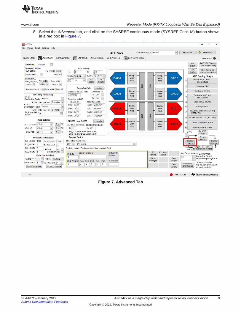
8. Select the Advanced tab, and click on the SYSREF continuous mode (SYSREF Cont. M) button shownin a red box in Figure 7.
Figure 7. Advanced Tab

Repeater Mode (RX-TX Loopback With SerDes Bypassed) www.ti.com
10 SLAA871–January 2019Submit Documentation Feedback
Copyright © 2019, Texas Instruments Incorporated
AFE74xx as a single-chip wideband repeater using loopback mode
9. In the Low Level View tab, click on the open folder icon, as shown in Figure 8.10. Load the loopback_mode_enable.cfg config file that was saved previously.
Figure 8. Low Level View Tab
www.ti.com Repeater Mode (RX-TX Loopback With SerDes Bypassed)
11SLAA871–January 2019Submit Documentation Feedback
Copyright © 2019, Texas Instruments Incorporated
AFE74xx as a single-chip wideband repeater using loopback mode
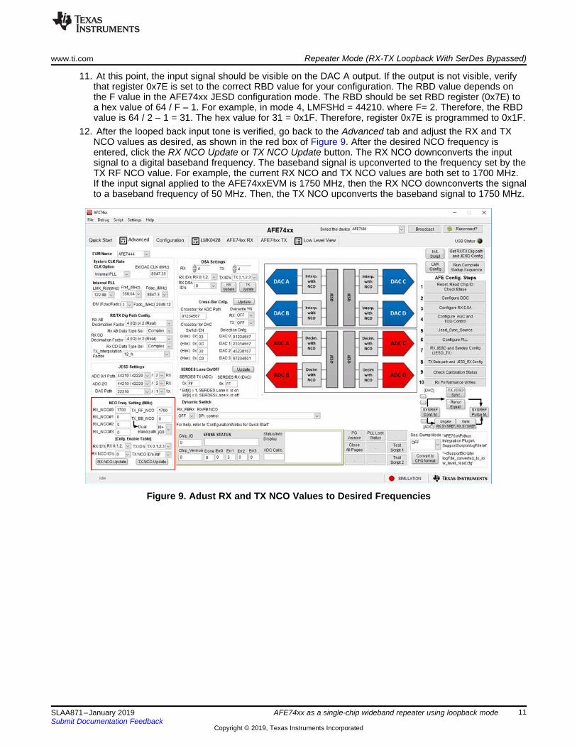
11. At this point, the input signal should be visible on the DAC A output. If the output is not visible, verifythat register 0x7E is set to the correct RBD value for your configuration. The RBD value depends onthe F value in the AFE74xx JESD configuration mode. The RBD should be set RBD register (0x7E) toa hex value of 64 / F – 1. For example, in mode 4, LMFSHd = 44210. where F= 2. Therefore, the RBDvalue is 64 / 2 – 1 = 31. The hex value for 31 = 0x1F. Therefore, register 0x7E is programmed to 0x1F.
12. After the looped back input tone is verified, go back to the Advanced tab and adjust the RX and TXNCO values as desired, as shown in the red box of Figure 9. After the desired NCO frequency isentered, click the RX NCO Update or TX NCO Update button. The RX NCO downconverts the inputsignal to a digital baseband frequency. The baseband signal is upconverted to the frequency set by theTX RF NCO value. For example, the current RX NCO and TX NCO values are both set to 1700 MHz.If the input signal applied to the AFE74xxEVM is 1750 MHz, then the RX NCO downconverts the signalto a baseband frequency of 50 MHz. Then, the TX NCO upconverts the baseband signal to 1750 MHz.
Figure 9. Adust RX and TX NCO Values to Desired Frequencies

130-MHz Digital Repeater System Overview www.ti.com
12 SLAA871–January 2019Submit Documentation Feedback
Copyright © 2019, Texas Instruments Incorporated
AFE74xx as a single-chip wideband repeater using loopback mode
3 130-MHz Digital Repeater System OverviewIn this example, the AFE74xx is evaluated as a direct RF-sampling, single-chip 4T4R wideband repeater.The AFE74xx as a repeater supports signal bandwidths from 130 MHz to 1.2 GHz. The bandwidth ofoperation for the experiments conducted in this application report is 130 MHz. The goal for all wirelesscommunication systems is to effectively distribute signals to and from users while providing optimumcoverage. Such goals have driven the demand for systems to operate at higher data rates. Although notyet permanently decided, 5G is supposed to support peak data rates in the Gbps range and average userdata rates of up to 100 Mbps. To achieve these data rates, wide signal bandwidths of 500 MHz, 1 GHz,and even up to 2 GHz are required. The demand for wide-band RF repeaters capable of operating withsuch high bandwidths is sure to increase in order to achieve optimum coverage for wireless systems. Ingeneral, RF repeaters are located throughout cells where RF signal-path obstructions exist between usersand base stations. A few different repeater types follow:• Analog: performs analog processing on received signal• Digital: performs digital processing on received signal• On-frequency: retransmits frequency on the same frequency that it was received• Off-frequency: retransmits frequency on frequency other than the received signal
Typical repeater systems configurations are 4T4R made up of four 1T1R or two 2T2R subsystems. Thisapplication report showcases the AFE74xx as an integrated, single-chip, 4T4R, digital wideband repeater.
3.1 Key System SpecificationsTable 2 shows the key system specifications.
Table 2. Key System Specifications
Parameter Specifications
Selectivity –50 dBc at +23 MHz offset from effective decimation bandwidth –70 dBc + 30MHz offset from effective decimation bandwidth
Effective decimation bandwidth 131.07 MHzAdjacent-channel power ratio (ACPR) degradation approximately 9.5 dBLatency 1.12 µsMaximum gain 9 dBm
DUC Block NCO_TX0
Interpolate-by-N
DDC Block
PA LNA
ADC DAC
ComplexMixer
Decimate-by-N ComplexMixer
NCO_RX0 DDC Block
N N
www.ti.com System Overview
13SLAA871–January 2019Submit Documentation Feedback
Copyright © 2019, Texas Instruments Incorporated
AFE74xx as a single-chip wideband repeater using loopback mode
4 System Overview
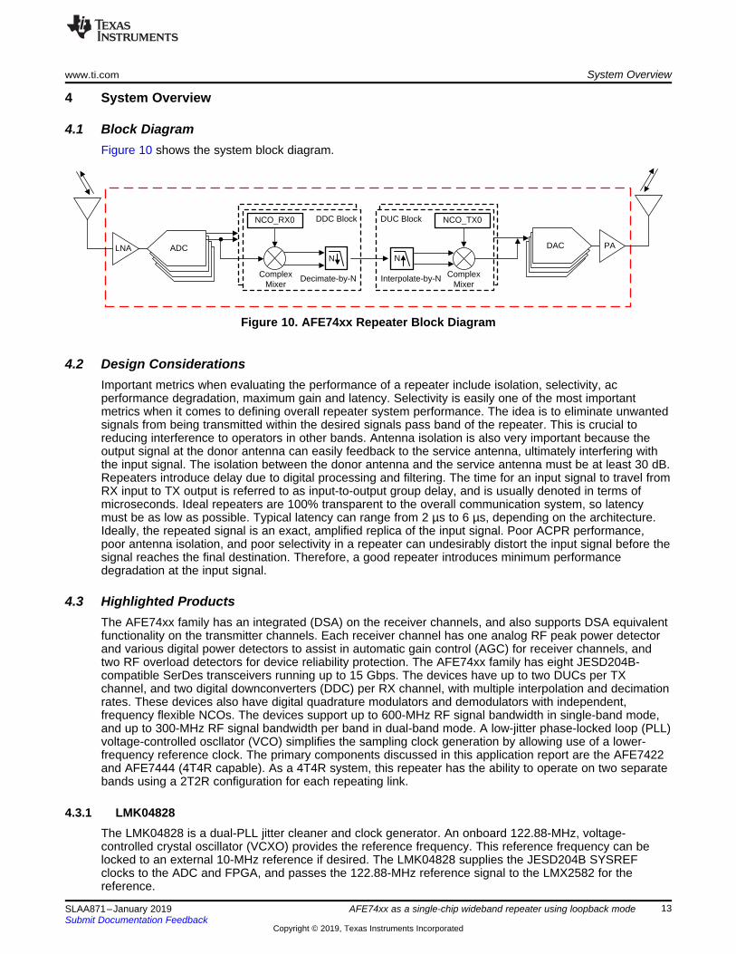
4.1 Block DiagramFigure 10 shows the system block diagram.
Figure 10. AFE74xx Repeater Block Diagram
4.2 Design ConsiderationsImportant metrics when evaluating the performance of a repeater include isolation, selectivity, acperformance degradation, maximum gain and latency. Selectivity is easily one of the most importantmetrics when it comes to defining overall repeater system performance. The idea is to eliminate unwantedsignals from being transmitted within the desired signals pass band of the repeater. This is crucial toreducing interference to operators in other bands. Antenna isolation is also very important because theoutput signal at the donor antenna can easily feedback to the service antenna, ultimately interfering withthe input signal. The isolation between the donor antenna and the service antenna must be at least 30 dB.Repeaters introduce delay due to digital processing and filtering. The time for an input signal to travel fromRX input to TX output is referred to as input-to-output group delay, and is usually denoted in terms ofmicroseconds. Ideal repeaters are 100% transparent to the overall communication system, so latencymust be as low as possible. Typical latency can range from 2 µs to 6 µs, depending on the architecture.Ideally, the repeated signal is an exact, amplified replica of the input signal. Poor ACPR performance,poor antenna isolation, and poor selectivity in a repeater can undesirably distort the input signal before thesignal reaches the final destination. Therefore, a good repeater introduces minimum performancedegradation at the input signal.
4.3 Highlighted ProductsThe AFE74xx family has an integrated (DSA) on the receiver channels, and also supports DSA equivalentfunctionality on the transmitter channels. Each receiver channel has one analog RF peak power detectorand various digital power detectors to assist in automatic gain control (AGC) for receiver channels, andtwo RF overload detectors for device reliability protection. The AFE74xx family has eight JESD204B-compatible SerDes transceivers running up to 15 Gbps. The devices have up to two DUCs per TXchannel, and two digital downconverters (DDC) per RX channel, with multiple interpolation and decimationrates. These devices also have digital quadrature modulators and demodulators with independent,frequency flexible NCOs. The devices support up to 600-MHz RF signal bandwidth in single-band mode,and up to 300-MHz RF signal bandwidth per band in dual-band mode. A low-jitter phase-locked loop (PLL)voltage-controlled oscllator (VCO) simplifies the sampling clock generation by allowing use of a lower-frequency reference clock. The primary components discussed in this application report are the AFE7422and AFE7444 (4T4R capable). As a 4T4R system, this repeater has the ability to operate on two separatebands using a 2T2R configuration for each repeating link.
4.3.1 LMK04828The LMK04828 is a dual-PLL jitter cleaner and clock generator. An onboard 122.88-MHz, voltage-controlled crystal oscillator (VCXO) provides the reference frequency. This reference frequency can belocked to an external 10-MHz reference if desired. The LMK04828 supplies the JESD204B SYSREFclocks to the ADC and FPGA, and passes the 122.88-MHz reference signal to the LMX2582 for thereference.

FPGA
LO
LO
ADC
ADC
DAC PA
DAC PA
LNA
LNA
MixerMixer
Mixer Mixer
Dual ADCs Dual DACs
System Overview www.ti.com
14 SLAA871–January 2019Submit Documentation Feedback
Copyright © 2019, Texas Instruments Incorporated
AFE74xx as a single-chip wideband repeater using loopback mode
4.4 System Design TheoryA digital RF repeater accomplishes the following goals:• Shows good selectivity by eliminating unwanted signals from being transmitted within the desired
signals passband, which reduces interference in other bands• Shows good antenna isolation between the donor and the service antenna• Has low RX to TX latency• Shows low ac-performance degradation.
Figure 11 shows the basic, traditional, RF-repeater design architecture.
Figure 11. Traditional Digital RF Repeater
The traditional repeater architecture first conditions the input signal using filters and LNAs. The localoscillator (LO) mixer downconverts the band to an intermediate frequency. The signal is filtered, sampled,and then sent to an FPGA for digital processing. The downmixing process is then reversed, and the finalsignal is output through the donor antenna to the desired base station.
All of the frequency translation functions of the traditional RF repeater are performed in the digital domainof the integrated AFE74xx system. This system replaces the need for discrete mixers, IF filters, and LOs(PLLs) from the analog-signal chain in order to achieve direct synthesis.

Agilent E5071B
Network Analyzer
Port 1
Port 2
www.ti.com Hardware and Testing
15SLAA871–January 2019Submit Documentation Feedback
Copyright © 2019, Texas Instruments Incorporated
AFE74xx as a single-chip wideband repeater using loopback mode
5 Hardware and Testing
5.1 Measured Latency and GainThe goal of this measurement is to evaluate the group delay and maximum gain of the RX-TX repeaterusing an Agilent E5071B network analyzer.
5.1.1 HardwareThe hardware used to test is as follows:• Rohde and Schwarz SMA 100 signal generator• DAC38RF82 RF DAC EVM• Agilent E4443A spectrum analyzer• Agilent E5071B network analyzer
5.1.2 Test Setup and ResultsFigure 12 shows the setup. Port 1 drives the input of the repeater with frequencies ranging from 1900MHz to 1920 MHz, and port 2 receives the signals from port 1, documenting the time of flight from Port 1to Port 2. The average group delay is approximately 1.12 µs. Figure 13 shows a graph of latency as afunction of frequencies between 1900 MHz and 1920 MHz.
The maximum gain was determined using the same setup as group delay and is approximately 9 dBmwhen both of the RX and TX DSA settings are set to 0. Figure 14 shows a graph of gain versesfrequencies between 1900 MHz and 1910 MHz.
Figure 12. Latency and Gain Test Setup
Figure 13. Latency Measurement,Average Latency = 1.12 µs
Figure 14. Gain Measurement: Gain is Flat at 9 dBmWith TX/RX DSA Set to 0

Agilent E4443A Spectrum Analyzer
1900 MHzBW = 85 MHz
DAC38RF82 RF DAC
Hardware and Testing www.ti.com
16 SLAA871–January 2019Submit Documentation Feedback
Copyright © 2019, Texas Instruments Incorporated
AFE74xx as a single-chip wideband repeater using loopback mode
5.2 Measured Linearity PerformanceThe goal of this measurement is to evaluate the transparency of the repeater by showing the ACPRdegradation of a signal through loopback.
5.2.1 Hardware and Test SetupThe DAC38RF82 is an RF DAC that generates the signal of the ACPR performance measurements.When measuring ACPR degradation, the RF DAC outputs a clean 20-MHz long-term evolution (LTE)signal centered at 1907 MHz. The output signal of the DAC first passes through a band-pass filter beforebeing connected to the input of the repeater.
Figure 15 shows the test setup for ACPR degradation. The ACPR of the LTE waveform is measureddirectly at the output of the DAC and also at the output of the repeater using the spectrum analyzer. Thecomparative difference in ACPR is the degradation of the LTE waveform due to the repeater.
Figure 15. Test Setup for ACPR Degradation
5.2.2 Test ResultsFigure 16 and Figure 17 show that the before and after LTE ACPR measurements of the repeater areapproximately 73 dB and 65 dB, respectively. The ACPR degradation caused by the receiver isapproximately 9 dBm. Notice that the reference level offset in Figure 17 increased by 2 dB to account forthe loss due to the filter and the extra SMA cables. The RX and TX DSAs were set to 1 and 0,respectively, in order to yield an overall gain of 6 dB.
Figure 16. Clean ACPR Measurement Directly FromDAC38RF82
Figure 17. Repeater ACPR Measurement From OutputShows 6-dB Gain of Waveform and 8-dB ACPR
Degradation

Splitter
Agilent E4443A Spectrum Analyzer
DAC38RF82 RF DAC
Rohde and Schwarz SMA 100A Signal Generator
www.ti.com Hardware and Testing
17SLAA871–January 2019Submit Documentation Feedback
Copyright © 2019, Texas Instruments Incorporated
AFE74xx as a single-chip wideband repeater using loopback mode
5.3 Measured Selectivity (Out-of-Band Jammer)The goal of this measurement is to characterize the in-band selectivity by sweeping a jammer in thetransition band of the repeater and recording the rolloff. Digital processing takes place in the on-chip DDCand digital upconverter (DUC). Therefore, the transition-band rolloff is fully dependent on the interpolationand decimation filters.
5.3.1 Hardware and Test SetupA DAC38RF82 is used to generate two 20-MHz LTE carriers spaced at 100 MHz and centered at 1870MHz. The LTE carriers simulate a 120-MHz wideband signal. A jammer signal is simulated by a CW toneproduced by a SMA Rhode and Schwartz signal generator. A 350-MHz to 6-GHz, mini-circuits powersplitter combines the wideband signal and CW tone to the input of the repeater. Figure 18 shows a blockdiagram of the setup.
Figure 18. Hardware Setup for Jammer Simulation
5.3.2 Test ResultsFigure 19 shows a repeated 120-MHz wideband signal at the output of the repeater without the jammerpresent. Figure 20 shows the jammer swept from the edge of the effective decimation pass band, throughthe transition band until the jammer is fully attenuated. The resulting measurement shows –50 dBc ofattenuation at 23 MHz, as denoted by marker 2.
Figure 19. Repeated Wideband Signal Simulatinga 120-MHz Carrier
Figure 20. –50-dBc Attenuation at 23-MHz OutsideDecimation Bandwidth

Terminology www.ti.com
18 SLAA871–January 2019Submit Documentation Feedback
Copyright © 2019, Texas Instruments Incorporated
AFE74xx as a single-chip wideband repeater using loopback mode
6 TerminologyDownlink: Traffic transmitter for the communication link, with respective to the main data source at theservice provider
TX: Traffic transmitter for the communication link
TXDAC: Digital-to-analog converter used for traffic transmitter
Uplink: Traffic receiver for the communication link, with respective to the main data source at the serviceprovider.
RX: Traffic receiver for the communication link
RXADC: Analog-to-digital converter used for traffic receiver or feedback receiver
DPD: Digital predistortion for power amplifier linearization
PA: Power amplifier for transmitter link
LNA: Low-noise amplifier for receiver link
DAS: Distributed antenna system
MU: Master unit in DAS
RU: Remote unit in DAS
BTS: Base station unit
MIMO: Multiple-input-multiple-output
JESD204B: JEDEC standard for high-speed serial link for data converters.
PLL: Phase-locked loop

IMPORTANT NOTICE AND DISCLAIMER
TI PROVIDES TECHNICAL AND RELIABILITY DATA (INCLUDING DATASHEETS), DESIGN RESOURCES (INCLUDING REFERENCEDESIGNS), APPLICATION OR OTHER DESIGN ADVICE, WEB TOOLS, SAFETY INFORMATION, AND OTHER RESOURCES “AS IS”AND WITH ALL FAULTS, AND DISCLAIMS ALL WARRANTIES, EXPRESS AND IMPLIED, INCLUDING WITHOUT LIMITATION ANYIMPLIED WARRANTIES OF MERCHANTABILITY, FITNESS FOR A PARTICULAR PURPOSE OR NON-INFRINGEMENT OF THIRDPARTY INTELLECTUAL PROPERTY RIGHTS.These resources are intended for skilled developers designing with TI products. You are solely responsible for (1) selecting the appropriateTI products for your application, (2) designing, validating and testing your application, and (3) ensuring your application meets applicablestandards, and any other safety, security, or other requirements. These resources are subject to change without notice. TI grants youpermission to use these resources only for development of an application that uses the TI products described in the resource. Otherreproduction and display of these resources is prohibited. No license is granted to any other TI intellectual property right or to any thirdparty intellectual property right. TI disclaims responsibility for, and you will fully indemnify TI and its representatives against, any claims,damages, costs, losses, and liabilities arising out of your use of these resources.TI’s products are provided subject to TI’s Terms of Sale (www.ti.com/legal/termsofsale.html) or other applicable terms available either onti.com or provided in conjunction with such TI products. TI’s provision of these resources does not expand or otherwise alter TI’s applicablewarranties or warranty disclaimers for TI products.
Mailing Address: Texas Instruments, Post Office Box 655303, Dallas, Texas 75265Copyright © 2019, Texas Instruments Incorporated