
afe5801
46
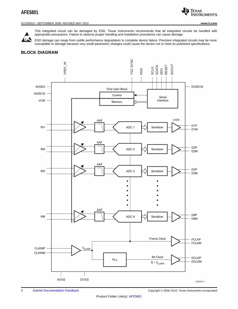
AFE5801 www.ti.com SLOS591D – SEPTEMBER 2008 – REVISED MAY 2010 8-Channel Variable-Gain Amplifier (VGA) With Octal High-Speed ADC Check for Samples: AFE5801 1FEATURES RELATED DEVICES • AFE5851: 16-Channel VGA + ADC, • Eight Variable-Gain Amplifiers (VGA) 32.5MSPS/Channel – Eight Differential Buffered Inputs With 2Vpp Maximum Swing DESCRIPTION – 5.5nV/√Hz VCA Input Noise (31dB Gain) The AFE5801 is an analog front end, targeting – Variable Gain, –5dB to 31dB With 0.125dB applications where the power and level of integration or 1dB Steps are critical. The device contains eight variable-gain – Digital Gain Control amplifiers (VGA), each followed by a high-speed (up to 65MSPS) ADC, for a total of eight ADCs per • Third-Order Antialiasing Filter With device. Programmable Cutoff Frequency (7.5, 10, or 14MHz) Each of the eight differential inputs is buffered, accepts up to 2Vpp maximum input swing, and is • Clamping followed by a VGA with a gain range from –5dB to • Analog-to-Digital Converter (ADC) 31dB. The VGA gain is digitally controlled, and the – Octal Channel, 12Bit, 65MSPS gain curves versus time can be stored in memory – Internal and External Reference Support integrated within the device using the serial interface. – No External Decoupling Required for A selectable clamping and antialias low-pass filter References (with 3dB attenuation at 7.5, 10, or 14MHz) is also integrated between VGA and ADC, for every channel. – Serial LVDS Outputs • 1.8V and 3.3V Supplies The VGA/antialias filter outputs are differential (limited to 2Vpp) and drive the onboard 12bit, • 50mW Total Power per Channel at 30MSPS 65MSPS ADC. The ADC also scales down its power • 58mW Total Power per Channel at 50MSPS consumption should a lower sampling rate be • 64QFN Package (9mm × 9mm) selected. The ADC outputs are serialized in LVDS streams, which further minimizes power and board APPLICATIONS area. • Imaging: Ultrasound, PET The AFE5801 is available in a 64-pin QFN package (9mm × 9mm) and is specified over the full industrial temperature range (–40°C to 85°C). 1 Please be aware that an important notice concerning availability, standard warranty, and use in critical applications of Texas Instruments semiconductor products and disclaimers thereto appears at the end of this data sheet. PRODUCTION DATA information is current as of publication date. Copyright © 2008–2010, Texas Instruments Incorporated Products conform to specifications per the terms of the Texas Instruments standard warranty. Production processing does not necessarily include testing of all parameters.
-
Upload
pieter-van-rooyen -
Category
Documents
-
view
212 -
download
0
description
APPLICATIONS DESCRIPTION AFE5801 www.ti.com SLOS591D – SEPTEMBER 2008 – REVISED MAY 2010 Please be aware that an important notice concerning availability, standard warranty, and use in critical applications of Texas Instruments semiconductor products and disclaimers thereto appears at the end of this data sheet. Check for Samples: AFE5801 Copyright © 2008–2010, Texas Instruments Incorporated PRODUCTION DATA information is current as of publication date. 1
Transcript of afe5801

AFE5801
www.ti.com SLOS591D –SEPTEMBER 2008–REVISED MAY 2010
8-Channel Variable-Gain Amplifier (VGA) With Octal High-Speed ADCCheck for Samples: AFE5801
1FEATURES RELATED DEVICES• AFE5851: 16-Channel VGA + ADC,• Eight Variable-Gain Amplifiers (VGA)
32.5MSPS/Channel– Eight Differential Buffered Inputs With 2VppMaximum Swing
DESCRIPTION– 5.5nV/√Hz VCA Input Noise (31dB Gain)
The AFE5801 is an analog front end, targeting– Variable Gain, –5dB to 31dB With 0.125dBapplications where the power and level of integrationor 1dB Stepsare critical. The device contains eight variable-gain
– Digital Gain Control amplifiers (VGA), each followed by a high-speed (upto 65MSPS) ADC, for a total of eight ADCs per• Third-Order Antialiasing Filter Withdevice.Programmable Cutoff Frequency (7.5, 10, or
14MHz) Each of the eight differential inputs is buffered,accepts up to 2Vpp maximum input swing, and is• Clampingfollowed by a VGA with a gain range from –5dB to• Analog-to-Digital Converter (ADC)31dB. The VGA gain is digitally controlled, and the
– Octal Channel, 12Bit, 65MSPS gain curves versus time can be stored in memory– Internal and External Reference Support integrated within the device using the serial interface.– No External Decoupling Required for A selectable clamping and antialias low-pass filter
References (with 3dB attenuation at 7.5, 10, or 14MHz) is alsointegrated between VGA and ADC, for every channel.– Serial LVDS Outputs
• 1.8V and 3.3V Supplies The VGA/antialias filter outputs are differential(limited to 2Vpp) and drive the onboard 12bit,• 50mW Total Power per Channel at 30MSPS65MSPS ADC. The ADC also scales down its power• 58mW Total Power per Channel at 50MSPS consumption should a lower sampling rate be
• 64QFN Package (9mm × 9mm) selected. The ADC outputs are serialized in LVDSstreams, which further minimizes power and board
APPLICATIONS area.• Imaging: Ultrasound, PET The AFE5801 is available in a 64-pin QFN package
(9mm × 9mm) and is specified over the full industrialtemperature range (–40°C to 85°C).
1
Please be aware that an important notice concerning availability, standard warranty, and use in critical applications of TexasInstruments semiconductor products and disclaimers thereto appears at the end of this data sheet.
PRODUCTION DATA information is current as of publication date. Copyright © 2008–2010, Texas Instruments IncorporatedProducts conform to specifications per the terms of the TexasInstruments standard warranty. Production processing does notnecessarily include testing of all parameters.
SerialInterface
Time Gain Block
CLKINP
CLKINM
PLLBit Clock
Frame Clock FCLKP
FCLKM
DCLKP
DCLKM
AVDD3
AVDD18
DVDD18
fCLKIN
6 f´ CLKIN
ADC 1 Serializer
LVDSAAF
IN1D1P
D1M
SD
OU
T
RE
SE
T
SE
N
SD
ATA
SC
LK
PD
N
TG
C S
YN
C
Control
Memory
ADC 2 Serializer
AAF
IN2D2P
D2M
ADC 3 Serializer
AAF
IN3D3P
D3M
·
·
·
·
·
·
·
·
·
·
·
·
ADC 8 Serializer
AAF
IN8D8P
D8M
B0328-01
VCM
VR
EF
_IN
AVSS DVSS
AFE5801
SLOS591D –SEPTEMBER 2008–REVISED MAY 2010 www.ti.com
This integrated circuit can be damaged by ESD. Texas Instruments recommends that all integrated circuits be handled withappropriate precautions. Failure to observe proper handling and installation procedures can cause damage.
ESD damage can range from subtle performance degradation to complete device failure. Precision integrated circuits may be moresusceptible to damage because very small parametric changes could cause the device not to meet its published specifications.
BLOCK DIAGRAM
2 Submit Documentation Feedback Copyright © 2008–2010, Texas Instruments Incorporated
Product Folder Link(s): AFE5801
AFE5801
QFN-649mm × 9mm
48
47
46
45
44
43
42
41
40
39
38
37
36
35
34
33
RGC PACKAGE(TOP VIEW)
1
2
3
4
5
6
7
8
9
10
11
12
13
14
15
1617
64
18
63
19
62
20
61
21
60
22
59
23
58
24
57
25
56
26
55
27
54
28
53
29
52
30
51
31
50
32
49
P0056-13
VC
M
AV
DD
3
AV
DD
18
CL
KIN
M
AV
SS
DV
DD
18
D8
M
D8
P
VR
EF
_IN NC
RE
SE
T
SC
LK
IN1P D2P
D5M
NC
AV
SS
VC
M
D1M
IN1M
IN2P
IN3P
IN2M
IN4P
IN3M
IN4M
DV
SS
D1
P
DV
DD
18
D3M
D4M
D4P
DCLKM
DCLKP
FCLKP
D7M
IN7M
IN7P
D6M
D6P
CL
KIN
P
IN6M
D7P
AV
SS
DV
DD
18
DV
SS
IN8P
IN8M
NC
AV
DD
18
FCLKM
D5P
PD
N
SY
NC
IN5P
SD
OU
T
AV
DD
18
AV
SS
IN5M
IN6P
D2M
D3P
SE
N
SD
ATA
AFE5801
www.ti.com SLOS591D –SEPTEMBER 2008–REVISED MAY 2010
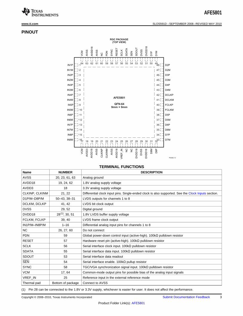
PINOUT
TERMINAL FUNCTIONSName NUMBER DESCRIPTION
AVSS 20, 23, 61, 63 Analog ground
AVDD18 19, 24, 62 1.8V analog supply voltage
AVDD3 18 3.3V analog supply voltage
CLKINP, CLKINM 21, 22 Differential clock input pins. Single-ended clock is also supported. See the Clock Inputs section.
D1P/M–D8P/M 50–43, 38–31 LVDS outputs for channels 1 to 8
DCLKM, DCLKP 41, 42 LVDS bit clock output
DVSS 29, 52 Digital ground
DVDD18 28 (1), 30, 51 1.8V LVDS buffer supply voltage
FCLKM, FCLKP 39, 40 LVDS frame clock output
IN1P/M–IN8P/M 1–16 Differential analog input pins for channels 1 to 8
NC 26, 27, 60 Do not connect
PDN 59 Global power-down control input (active-high). 100kΩ pulldown resistor
RESET 57 Hardware reset pin (active-high). 100kΩ pulldown resistor
SCLK 56 Serial interface clock input. 100kΩ pulldown resistor
SDATA 55 Serial interface data input. 100kΩ pulldown resistor
SDOUT 53 Serial interface data readout
SEN 54 Serial interface enable. 100kΩ pullup resistor
SYNC 58 TGC/VGA synchronization signal input. 100kΩ pulldown resistor
VCM 17, 64 Common-mode output pins for possible bias of the analog input signals
VREF_IN 25 Reference input in the external reference mode
Thermal pad Bottom of package Connect to AVSS
(1) Pin 28 can be connected to the 1.8V or 3.3V supply, whichever is easier for user. It does not affect the performance.
Copyright © 2008–2010, Texas Instruments Incorporated Submit Documentation Feedback 3
Product Folder Link(s): AFE5801

AFE5801
SLOS591D –SEPTEMBER 2008–REVISED MAY 2010 www.ti.com
PACKAGING/ORDERING INFORMATION (1)
PRODUCT PACKAGE-LEAD PACKAGE SPECIFIED PACKAGE ORDERING TRANSPORTDESIGNATOR TEMPERATURE MARKING NUMBER MEDIA,
RANGE QUANTITY
AFE5801 QFN-64 (2) RGC –40°C to 85°C AFE5801 AFE5801IRGCT Tape/reel, 250
AFE5801 QFN-64 (2) RGC –40°C to 85°C AFE5801 AFE5801IRGCR Tape/reel, 2000
(1) For the most-current package and ordering information, see the Package Option Addendum at the end of this document, or see the TIWeb site at www.ti.com.
(2) For the thermal pad size on the package, see the mechanical drawings at the end of this document.
ABSOLUTE MAXIMUM RATINGS (1)
over operating free-air temperature range (unless otherwise noted)
VALUE UNIT
AVDD3 to AVSS –0.3 to 3.8 V
AVDD18 to AVSS –0.3 to 2.2 V
DVDD18 to DVSS –0.3 to 2.2 V
Voltage between AVSS and DVSS –0.3 to 0.3 V
Analog input pins (INiP, INiM) to AVSS –0.3V to MIN (3.6V, AVDD3 + 0.3V) V
VREF_IN to AVSS –0.3 to 2.2 V
VCLKP, VCLKM to AVSS –0.3 to 2.2 V
Digital control pins to DVSS: PDN, RESET, SCLK, SDATA, SEN, SYNC –0.3 to 3.6 V
TJ Maximum operating junction temperature 125 °C
Tstg Storage temperature range –60 to 150 °C
(1) Stresses beyond those listed under Absolute Maximum Ratings may cause permanent damage to the device. These are stress ratingsonly, and functional operation of the device at these or any other conditions beyond those indicated under Recommended OperatingConditions is not implied. Exposure to absolute-maximum-rated conditions for extended periods may affect device reliability.
THERMAL CHARACTERISTICSPARAMETER TEST CONDITIONS TYP UNIT
qJA 0 LFM air flow 23.17 °C/W
qJC 2-oz. (0.071-mm thick) copper trace and pad soldered directly to a JEDEC-standard four-layer 22.1 °C/W3-in. × 3-in. (7.62-cm ×7.62-cm) PCB.
RECOMMENDED OPERATING CONDITIONSMIN TYP MAX UNIT
TA Ambient temperature –40 85 °C
SUPPLIES
AVDD3 Analog supply voltage (VGA) 3 3.3 3.6 V
AVDD18 Analog supply voltage (ADC) 1.7 1.8 1.9 V
DVDD18 Digital supply voltage (ADC, LVDS) 1.7 1.8 1.9 V
ANALOG INPUTS
INiP, INiM Input voltage range to AVSS VCM – 0.5 VCM + 0.5 V
VREF_IN in external reference mode 1.35 1.4 1.45 V
VCM load 3 mA
4 Submit Documentation Feedback Copyright © 2008–2010, Texas Instruments Incorporated
Product Folder Link(s): AFE5801
AFE5801
www.ti.com SLOS591D –SEPTEMBER 2008–REVISED MAY 2010
RECOMMENDED OPERATING CONDITIONS (continued)MIN TYP MAX UNIT
CLOCK INPUT
fCLKIN Input clock frequency 5 65 MSPS
Input clock duty cycle 40% 50% 60%
Sine wave, ac-coupled 0.5 Vpp
VCLKP-CLKM LVPECL, ac-coupled 1.6 Vpp
LVDS, ac-coupled 0.25 0.7 Vpp
VCLKP LVCMOS, single-ended, VCLKM to AVSS 1.8 Vpp
VIH High-level input voltage 0.75 × AVDD18 V
VIL Low-level input voltage 0.25 × AVDD18 V
DIGITAL OUTPUT
CLOAD External load capacitance from each output pin to DVSS 5 pF
RLOAD Differential load resistance (external) between the LVDS output pairs 100 Ω
ELECTRICAL CHARACTERISTICSTypical values are at 25°C, MIN and MAX values are across the full temperature range of Tmin = –40°C to Tmax = 85°C,AVDD3 = 3.3V, AVDD18 = 1.8V, DVDD18 = 1.8V, –1dBFS analog input ac-coupled with 0.1mF, internal reference mode,maximum-rated sampling frequency (65MSPS), LVCMOS (single-ended) clock, 50% duty cycle, antialiasing filter set at14MHz (3dB corner), output clamp disabled (1) and analog high-pass filter enabled, unless otherwise noted.
PARAMETER TEST CONDITIONS MIN TYP MAX UNIT
VARIABLE GAIN AMPLIFIER (VGA)
Maximum input voltage swing Linear operation, from INP to INM 2 Vpp
VCM Common-mode voltage 1.6 V
Gain range Maximum gain – minimum gain 36 dB
Maximum gain 29.5 31 32.5 dB
0.125Gain resolution dBor 1
Input resistance From each input to dc bias level 5 kΩInput capacitance Differential between the inputs 2 pF
ANTIALIAS FILTER (AAF)
7.5MHz filter selected 7.5
AAF cutoff frequency 10MHz filter selected –3dB 10 MHz
14MHz filter selected 14
7.5MHz filter selected 10
10MHz filter selected –6dB 14 MHz
14MHz filter selected 20AAF stop-band attenuation
7.5MHz filter selected 18
10MHz filter selected –12dB 24 MHz
14MHz filter selected 30
7.5MHz filter selected 1.2
In-band attenuation 10MHz filter selected At 3.2MHz 0.5 dB
14MHz filter selected 0.2
(1) Enabling clamping increases distortion values at high swings by about 2dB.
Copyright © 2008–2010, Texas Instruments Incorporated Submit Documentation Feedback 5
Product Folder Link(s): AFE5801
AFE5801
SLOS591D –SEPTEMBER 2008–REVISED MAY 2010 www.ti.com
ELECTRICAL CHARACTERISTICS (continued)Typical values are at 25°C, MIN and MAX values are across the full temperature range of Tmin = –40°C to Tmax = 85°C,AVDD3 = 3.3V, AVDD18 = 1.8V, DVDD18 = 1.8V, –1dBFS analog input ac-coupled with 0.1mF, internal reference mode,maximum-rated sampling frequency (65MSPS), LVCMOS (single-ended) clock, 50% duty cycle, antialiasing filter set at14MHz (3dB corner), output clamp disabled (1) and analog high-pass filter enabled, unless otherwise noted.
PARAMETER TEST CONDITIONS MIN TYP MAX UNIT
FULL-CHANNEL CHARACTERISTICS
Gain matching Across channels and parts 0.1 0.6 dB
–5dB to 28dB gain –1.2 ±0.3 1.2Gain error dB
Gain > 28dB –1.8 ±0.5 1.8
Offset error 31dB gain –50 50 LSB
5MHz, 31dB VGA gain, low-noise mode 5 6.5 nV/√HzInput-referred noise voltage
5MHz, 31dB VGA gain, default noise mode 5.5 nV/√Hz
SNR Signal-to-noise ratio –1dBFS ADC input, 6dB gain 66 dBc
HD2 –1dBFS ADC input, 17dB gain, fin = 2MHz –75 –60Second-harmonic distortion dBc
–1dBFS ADC input, 31dB gain, fin = 2MHz –75 –60
–1dBFS ADC input, 17dB gain, fin = 2MHz –65 –55HD3 Third-harmonic distortion dBc
–1dBFS ADC input, 31dB gain, fin = 2MHz –60 –52
SFDR Spurious-free dynamic range –1dBFS ADC input, 17dB gain, fin = 2MHz 65 dBc
THD Total harmonic distortion –1dBFS ADC input, 17dB gain, fin = 2MHz 64 dBc
IMD Intermodulation distortion fin1 = 1MHz, fin2 = 2MHz, Ain1, in2 = –7dBFS, 30dB –70 dBFSVGA gain
Group delay variation f = 100kHz to 14MHz, across gain settings and ±3.5 nschannels
f = 100kHz to 14MHz, across channels ±1.5
ClockInput overload recovery ≤ 6dB overload to within 1% 1 cycle
Clamp level After amplification. Clamp enabled by default 3 dB
ADC number of bits 12
Aggressor: fin = 3MHz, 1dB below ADC full-scaleCrosstalk Victims (channel next to aggressor channel): 50Ω 92 dB
differential (between INiP and INiM)
POWER
Default noise mode 522 600Total power dissipation mW
Low-noise mode 561 636
IAVDD3 AVDD3 current consumption 6 9 mA
IAVDD18 AVDD18 current consumption Default noise mode 198 222mA
Low-noise mode 220 244
IDVDD18 DVDD18 current consumption See (2) 81 100 mA
Standby mode 64 mWPower down
Full power-down mode 8 25 mW
AC PSRR Power-supply rejection ratio 30 dBc
(2) Using digital modes like averaging, digital gain, digital HPF, etc., (see the Application Information section) might increase the DVDD18current by about 60mA.
6 Submit Documentation Feedback Copyright © 2008–2010, Texas Instruments Incorporated
Product Folder Link(s): AFE5801
AFE5801
www.ti.com SLOS591D –SEPTEMBER 2008–REVISED MAY 2010
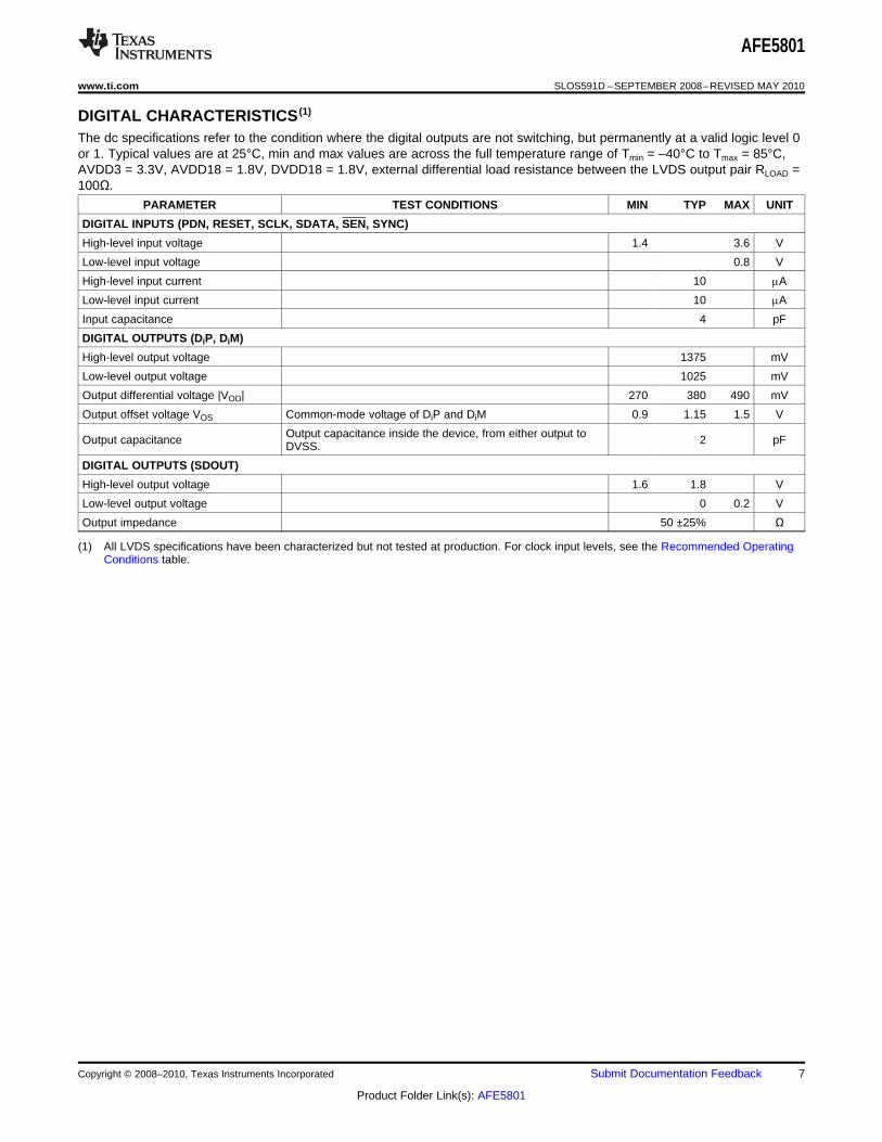
DIGITAL CHARACTERISTICS (1)
The dc specifications refer to the condition where the digital outputs are not switching, but permanently at a valid logic level 0or 1. Typical values are at 25°C, min and max values are across the full temperature range of Tmin = –40°C to Tmax = 85°C,AVDD3 = 3.3V, AVDD18 = 1.8V, DVDD18 = 1.8V, external differential load resistance between the LVDS output pair RLOAD =100Ω.
PARAMETER TEST CONDITIONS MIN TYP MAX UNIT
DIGITAL INPUTS (PDN, RESET, SCLK, SDATA, SEN, SYNC)
High-level input voltage 1.4 3.6 V
Low-level input voltage 0.8 V
High-level input current 10 mA
Low-level input current 10 mA
Input capacitance 4 pF
DIGITAL OUTPUTS (DiP, DiM)
High-level output voltage 1375 mV
Low-level output voltage 1025 mV
Output differential voltage |VOD| 270 380 490 mV
Output offset voltage VOS Common-mode voltage of DiP and DiM 0.9 1.15 1.5 V
Output capacitance inside the device, from either output toOutput capacitance 2 pFDVSS.
DIGITAL OUTPUTS (SDOUT)
High-level output voltage 1.6 1.8 V
Low-level output voltage 0 0.2 V
Output impedance 50 ±25% Ω
(1) All LVDS specifications have been characterized but not tested at production. For clock input levels, see the Recommended OperatingConditions table.
Copyright © 2008–2010, Texas Instruments Incorporated Submit Documentation Feedback 7
Product Folder Link(s): AFE5801

AFE5801
SLOS591D –SEPTEMBER 2008–REVISED MAY 2010 www.ti.com
OUTPUT INTERFACE TIMINGTypical values are at 25°C, AVDD3 = 3.3V, AVDD18 = DVDD = 1.8V, LVCMOS (single ended) clock, CLOAD = 5pF, RLOAD =100Ω, IO = 3.5mA, unless otherwise noted. Minimum and maximum values are across the full temperature range TMIN =–40°C to TMAX = 85°C.
PARAMETER TEST CONDITIONS MIN TYP MAX UNIT
The delay in time between the rising edge of the input samplingta Aperture delay 0.7 3 nsclock and the actual time at which the sampling occurs
Aperture delay matching Across channels within the same device ±150 ps
tj Aperture jitter 450 fs rms
Time to valid data after coming out of STANDBY mode 10 50
Wake-up time Time to valid data after coming out of PDN GLOBAL mode 50 200 ms
Time to valid data after stopping and restarting the input clock 30 200
InputADC latency Default, after reset 11 clock
cycles
Input clock rising edge (zero cross) to frame clock rising edge (zerotdelay Data and frame clock delay 3 4.7 6.4 nscross) minus half the input clock period (T).
Δtdelay Delay variation At fixed supply and 20°C T difference –1 1 ns
Rise time measured from –100mV to 100mVtRISE Data rise time
Fall time measured from 100mV to –100mV 0.1 0.25 0.4 nstFALL Data fall time
10MHz < fCLKIN < 65MHz
Rise time measured from –100mV to 100mVtFCLKRISE Frame clock rise time Fall time measured from 100mV to –100mV 0.1 0.25 0.4 nstFCLKFALL Frame clock fall time 10MHz < fCLKIN < 65MHz
Frame clock duty cycle Zero crossing of the rising edge to zero crossing of the falling edge 48% 50% 52%
Rise time measured from –100mV to 100mVtDCLKRISE Bit clock rise time Fall time measured from 100mV to –100mV 0.1 0.2 0.35 nstDCLKFALL Bit clock fall time 10MHz < fCLKIN < 65MHz
Zero crossing of the rising edge to zero crossing of the falling edgeBit clock duty cycle 44% 50% 56%10MHz < fCLKIN < 65MHz
Output Interface Timing (1)
Setup Time (tsu), Hold Time (th),fCLKIN, Input Clock Frequency Period (T) tpdi = 0.5 × T + tdelay, nsns ns
Input Clock Zero-Cross (risingZero-Cross Data to Zero-Cross Zero-Cross Clock to Zero-Cross edge) to Frame Clock Zero-CrossClock (both edges) Data (both edges)MHz ns (rising edge)
MIN TYP MAX MIN TYP MAX MIN TYP MAX
65 15 0.35 0.6 0.3 0.6 12.3
50 20 0.5 0.8 0.5 0.8 14.6
40 25 0.75 1 0.75 1 17
30 33 1 1.4 1 1.4 21.2
20 50 1.7 2.1 1.7 2.1 29.5
10 100 3.8 4.2 3.8 4.2 54.7
(1) FCLK timing is the same as for the output data lines. It has the same relation to DCLK as the data pins. Setup and hold are the samefor the data and the frame clock.
8 Submit Documentation Feedback Copyright © 2008–2010, Texas Instruments Incorporated
Product Folder Link(s): AFE5801
Fra
me
Clo
ck
FC
LK
Fre
q=
f CL
KIN
Inp
ut
Clo
ck
CLK
IN
Fre
q =
fC
LK
IN
SA
MP
LE
N–
1S
AM
PLE
N +
1
Data
Bit
inM
SB
FirstM
od
e
Data
Bit
inLS
BF
irst
Mode
Bit
Clo
ck
DC
LK
Fre
q=
6x
f CLK
IN
Outp
ut
Data
Ch
nO
UT
Da
tara
te=
12
xf C
LK
IN
SA
MP
LE
N
t pdi
Inp
utS
ign
al
t a
Sam
ple
NS
am
ple
N +
10
Sa
mp
leN
+ 1
1
11
Clo
ck
Cycle
sLate
ncy
SA
MP
LE
N–
11
D1
(D10)
D0
(D11)
D11
(D0)
D10
(D1)
D9
(D2)
D8
(D3)
D7
(D4)
D6
(D5)
D5
(D6)
D4
(D7)
D3
(D8)
D2
(D9)
D1
(D10)
D0
(D11)
D11
(D0)
D10
(D1)
D9
(D2)
D8
(D3)
D7
(D4)
D6
(D5)
D5
(D6)
D4
(D7)
D2
(D9)
D3
(D8)
D1
(D10)
D0
(D11)
D11
(D0)
D10
(D1)
D9
(D2)
D8
(D3)
D7
(D4)
D6
(D5)
D5
(D6)
D4
(D7)
D3
(D8)
D2
(D9)
D1
(D10)
D0
(D11)
D11
(D0)
D10
(D1)
D13
(D2)
T
T0434-0
1
Bit C
lock
DC
LK
P
Outp
ut D
ata
Pair
t su
CH
iout
t h
t ht s
u
DC
LK
M
Dn +
1D
n
AFE5801
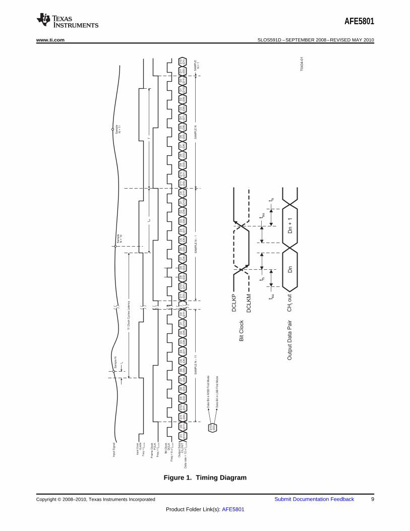
www.ti.com SLOS591D –SEPTEMBER 2008–REVISED MAY 2010
Figure 1. Timing Diagram
Copyright © 2008–2010, Texas Instruments Incorporated Submit Documentation Feedback 9
Product Folder Link(s): AFE5801

f − Frequency − MHz
−110
−90
−70
−50
−30
−10
10
0 5 10 15 20 25 30 35
Am
plitu
de −
dB
G001
Ain = −1dBFSGain = 12dBHD2 = −80.1dBcHD3 = −64.2dBcSFDR = 63.9dBcSNR = 65.9dBFSTHD = 63.9dBc
f − Frequency − MHz
−110
−90
−70
−50
−30
−10
10
0 5 10 15 20 25 30 35
Am
plitu
de −
dB
G002
Ain = −1dBFSGain = 30dBHD2 = −69.8dBcHD3 = −59.5dBcSFDR = 59.5dBcSNR = 58.8dBFSTHD = 58.9dBc
FINE_GAIN Register Setting
68
101214161820222426283032
0.000 0.125 0.250 0.375 0.500 0.625 0.750 0.875
G −
Gai
n −
dB
G021
Coarse Gain = 7dB
Coarse Gain = 31dB
Coarse Gain = 19dB
Gain Code
−8
−4
0
4
8
12
16
20
24
28
32
0 4 8 12 16 20 24 28 32 36
G −
Gai
n −
dB
G025
(Ideal+1dB) Line
(Ideal−1dB) Line
−40°C
25°C
85°C
G − Gain − dB
−1.0
−0.8
−0.6
−0.4
−0.2
0.0
0.2
0.4
0.6
0.8
1.0
−5 0 5 10 15 20 25 30
Gai
n E
rror
− d
B
G026
−40°C25°C
85°C
G − Gain − dB
45
65
85
105
125
145
165
185
−5 0 5 10 15 20 25 30
Out
put-
Ref
erre
d N
oise
− n
V/√
Hz
G022
Low-Noise Enabled
Low-Noise Disabled
AFE5801
SLOS591D –SEPTEMBER 2008–REVISED MAY 2010 www.ti.com
TYPICAL CHARACTERISTICSAll graphs are at 25°C, AVDD3 = 3.3V, AVDD18 = DVDD18 = 1.8V, –1dBFS analog input AC coupled with 0.1mF, internalreference mode, maximum rated channel sampling frequency (65MSPS), LVCMOS (single-ended) clock, 50% duty cycle,fIN = 2MHz, anti-aliasing filter set at 14MHz (3dB corner), output clamp disable and analog high-pass filter enabled. spacer
Figure 2. FFT for 2MHz Input Signal and 12dB Gain Figure 3. FFT for 2MHz Input Signal and 30dB Gain
Figure 4. Fine Gain vs Gain Code Figure 5. Gain vs Gain Code and Temperature
Figure 6. Gain Error vs Gain Code and Temperature Figure 7. Output-Referred Noise vs Gain
10 Submit Documentation Feedback Copyright © 2008–2010, Texas Instruments Incorporated
Product Folder Link(s): AFE5801

G − Gain − dB
8
18
28
38
48
58
68
78
88
98
−6 −4 −2 0 2 4 6 8 10 12 14 16 18
Inpu
t-R
efer
red
Noi
se −
nV
/√H
z
G023
Low-Power Mode Enabled
Low-Power Mode Disabled
G − Gain − dB
4
5
6
7
8
9
10
11
17 18 19 20 21 22 23 24 25 26 27 28 29 30 31
Inpu
t-R
efer
red
Noi
se −
nV
/√H
z
G024
Low-Power Mode Disabled
Low-Power Mode Enabled
G − Gain − dB
−90
−85
−80
−75
−70
−65
−60
−10 0 10 20 30 40
Ain = −1dBFS
HD
2 −
dBc
G003
fIN = 1MHz
fIN = 5MHz
fIN = 10MHz
G − Gain − dB
−90
−88
−86
−84
−82
−80
−78
−76
−74
−72
−70
−10 0 10 20 30 40
Ain = −6dBFSH
D2
− dB
c
G004
fIN = 5MHz
fIN = 1MHz
fIN = 10MHz
AFE5801
www.ti.com SLOS591D –SEPTEMBER 2008–REVISED MAY 2010
TYPICAL CHARACTERISTICS (continued)
All graphs are at 25°C, AVDD3 = 3.3V, AVDD18 = DVDD18 = 1.8V, –1dBFS analog input AC coupled with 0.1mF, internalreference mode, maximum rated channel sampling frequency (65MSPS), LVCMOS (single-ended) clock, 50% duty cycle,fIN = 2MHz, anti-aliasing filter set at 14MHz (3dB corner), output clamp disable and analog high-pass filter enabled. spacer
Figure 8. Input-Referred Noise for Low Gains Figure 9. Input-Referred Noise for High Gains
Figure 10. HD2 Across Coarse Gain and Three fIN Figure 11. HD2 Across Coarse Gain and Three fIN(–1dBFS) (1) (–6dBFS) (2)
(1) For gains ≥5dB, the input amplitude is adjusted to give –1dBFS. At 5dB gain, input amplitude is 4dBm (corresponding to –1dBFS).For gains less than 5dB, the input is kept constant at 4dBm.
(2) For gains ≥0dB, the input amplitude is adjusted to give –6dBFS. At 0dB gain, input amplitude is 4dBm (corresponding to –6dBFS).For gains less than 0dB, the input is kept constant at 4dBm.
Copyright © 2008–2010, Texas Instruments Incorporated Submit Documentation Feedback 11
Product Folder Link(s): AFE5801
G − Gain − dB
−70
−65
−60
−55
−50
−45
−40
−35
−30
−10 0 10 20 30 40
HD
3 −
dBc
G005
fIN = 10MHz
Ain = −1dBFS
fIN = 5MHz
fIN = 1MHz
G − Gain − dB
−100
−90
−80
−70
−60
−50
−40
−10 0 10 20 30 40
Ain = −6dBFS
HD
3 −
dBc
G006
fIN = 5MHzfIN = 10MHz
fIN = 1MHz
Output Amplitude − dBFS
−100
−90
−80
−70
−60
−50
−40
−30
−20
−70 −60 −50 −40 −30 −20 −10 0
fIN = 2MHz
HD
2 −
dB
G007
Gain = 18dB
Gain = 6dB
Gain = 30dB
Output Amplitude − dBFS
−100
−90
−80
−70
−60
−50
−40
−30
−70 −60 −50 −40 −30 −20 −10 0
HD
3 −
dB
G008
fIN = 2MHz
Gain = 18dB
Gain = 6dB
Gain = 30dB
Channel
−120
−110
−100
−90
−80
−70
−60
0 2 4 6 8 10
Am
plitu
de −
dB
c
G009
10MHz − Adjacent
3MHz − Adjacent 3MHz − Far
10MHz − Far
G − Gain − dB
2030
2040
2050
2060
2070
2080
2090
−5 0 5 10 15 20 25 30
Out
put O
ffset
− C
ode
G027
Analog HPF Disabled
Digital HPF Enabled
Analog HPF Enabled
AFE5801
SLOS591D –SEPTEMBER 2008–REVISED MAY 2010 www.ti.com
TYPICAL CHARACTERISTICS (continued)
All graphs are at 25°C, AVDD3 = 3.3V, AVDD18 = DVDD18 = 1.8V, –1dBFS analog input AC coupled with 0.1mF, internalreference mode, maximum rated channel sampling frequency (65MSPS), LVCMOS (single-ended) clock, 50% duty cycle,fIN = 2MHz, anti-aliasing filter set at 14MHz (3dB corner), output clamp disable and analog high-pass filter enabled. spacer
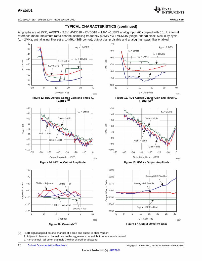
Figure 12. HD3 Across Coarse Gain and Three fIN Figure 13. HD3 Across Coarse Gain and Three fIN(–1dBFS)(1) (–6dBFS)(2)
Figure 14. HD2 vs Output Amplitude Figure 15. HD3 vs Output Amplitude
Figure 17. Output Offset vs GainFigure 16. Crosstalk (3)
(3) –1dB signal applied on one channel at a time and output is observed on:1. Adjacent channel - channel next to the aggressor channel, but not a shared channel2. Far channel - all other channels (neither shared or adjacent)
12 Submit Documentation Feedback Copyright © 2008–2010, Texas Instruments Incorporated
Product Folder Link(s): AFE5801

fIN − Input Frequency − MHz
−12−11−10−9−8−7−6−5−4−3−2−101
0 2 4 6 8 10 12 14 16 18 20
Nor
mal
ized
Am
plitu
de −
dB
G010
14MHz
7.5MHz
10MHz
f − Frequency − MHz
−70
−60
−50
−40
−30
−20
−10
0
10
20
0.0 0.5 1.0 1.5 2.0 2.5 3.0
G −
Gai
n −
dB
G011
K = 2dB
K = 3dBK = 5dB
K = 4dB
K = 6dB
K = 8dBK = 9dBK = 10dB
Analog FilterK = 7dB
f − Clock Frequency − MSPS
0
50
100
150
200
250
300
350
400
450
0 10 20 30 40 50 60 70
AV
DD
3 P
ower
− m
W
G012
AVDD Power − Default
fIN = 2MHz
AVDD Power − Low-Noise Mode
f − Clock Frequency − MSPS
0.30
0.35
0.40
0.45
0.50
0.55
0.60
5 10 15 20 25 30 35 40 45 50 55 60 65
P −
Tot
al P
ower
− m
W
G013
Total Power − Low-Noise Mode
Total Power − Default
fin = 2MHz
GAIN_MATCHING − dB
0
1
2
3
4
5
6
7
0.02 0.07 0.12 0.17 0.22 0.27 0.32 0.37 0.42 0.47 0.52
Ocu
rren
ces
− %
G030Output Code − Offset
0.0
0.5
1.0
1.5
2.0
2.5
3.0
3.5
4.0
2005 2016 2027 2038 2049 2060 2071 2072 2083
Cou
nt (
Num
ber
of C
hann
els)
− %
G031
AFE5801
www.ti.com SLOS591D –SEPTEMBER 2008–REVISED MAY 2010
TYPICAL CHARACTERISTICS (continued)
All graphs are at 25°C, AVDD3 = 3.3V, AVDD18 = DVDD18 = 1.8V, –1dBFS analog input AC coupled with 0.1mF, internalreference mode, maximum rated channel sampling frequency (65MSPS), LVCMOS (single-ended) clock, 50% duty cycle,fIN = 2MHz, anti-aliasing filter set at 14MHz (3dB corner), output clamp disable and analog high-pass filter enabled. spacer
Figure 18. Antialiasing Filter Frequency Response Figure 19. High-Pass Filter Options
Figure 20. Analog Power vs Input-Clock Frequency Figure 21. Total Power vs Input-Clock Frequency
Figure 22. Gain Matching Measured at a Single Gain (30 Figure 23. Offset (Average Code) With Signal. EverydB) as Peak-to-Peak Variation of Gain Across Channels Channel Counted as One Eventon Every Device and Measured at Three Temperatures.
Every Device at Each Temperature Counted as One Event
Copyright © 2008–2010, Texas Instruments Incorporated Submit Documentation Feedback 13
Product Folder Link(s): AFE5801
1000
1200
1400
1600
1800
2000
2200
2400
2600
2800
0 1000 2000 3000 4000 5000 6000 7000 8000
fIN = 2MHz
Sample
Out
put C
ode
G014
1000
1200
1400
1600
1800
2000
2200
2400
2600
2800
0 1000 2000 3000 4000 5000 6000 7000 8000
Sample
Out
put C
ode
G015
fIN = 2MHz
1000
1200
1400
1600
1800
2000
2200
2400
2600
2800
2500 3500 4500 5500 6500 7500 8500 9500
Sample
Out
put C
ode
G016
fIN = 2MHz
AFE5801
SLOS591D –SEPTEMBER 2008–REVISED MAY 2010 www.ti.com
TYPICAL CHARACTERISTICS (continued)
All graphs are at 25°C, AVDD3 = 3.3V, AVDD18 = DVDD18 = 1.8V, –1dBFS analog input AC coupled with 0.1mF, internalreference mode, maximum rated channel sampling frequency (65MSPS), LVCMOS (single-ended) clock, 50% duty cycle,fIN = 2MHz, anti-aliasing filter set at 14MHz (3dB corner), output clamp disable and analog high-pass filter enabled. spacer
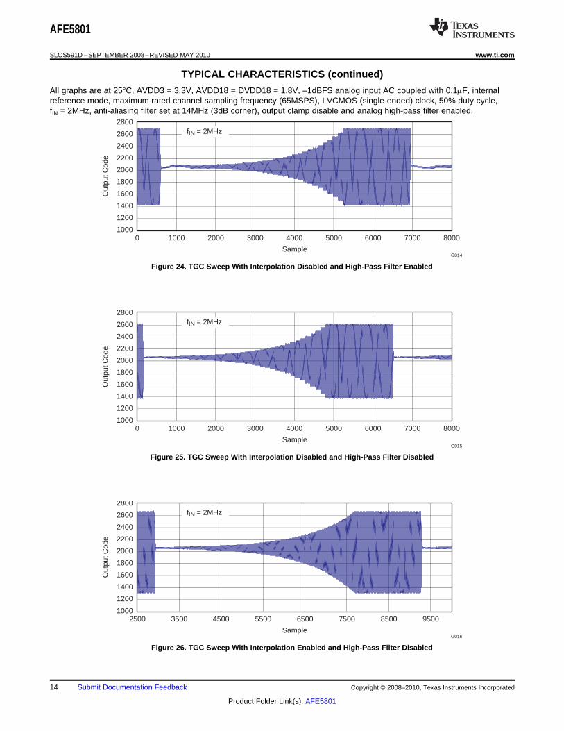
Figure 24. TGC Sweep With Interpolation Disabled and High-Pass Filter Enabled
Figure 25. TGC Sweep With Interpolation Disabled and High-Pass Filter Disabled
Figure 26. TGC Sweep With Interpolation Enabled and High-Pass Filter Disabled
14 Submit Documentation Feedback Copyright © 2008–2010, Texas Instruments Incorporated
Product Folder Link(s): AFE5801

−120
−100
−80
−60
−40
−20
0
0 5 10 15 20 25 30 35
f − Frequency − MHz
Am
plitu
de −
dB
G017
Gain = 30dBfIN1 = 2.92MHz at −7dBFSfIN2 = 3.12MHz at −7dBFSIMD3 = −70dBFS
f − Frequency − MHz
3
5
7
9
11
13
15
17
19
21
0.0 0.5 1.0 1.5 2.0 2.5 3.0
Inpu
t-R
efer
red
Noi
se −
nV
/√H
z
G018
Analog HPF Disabled
Default
High-Pass Digital Filter K = 4
Gain = 30dB
G − Gain − dB
58
59
60
61
62
63
64
65
66
67
−10 0 10 20 30 40
Ain = −1dBFS
SN
R −
dB
FS
G019
fIN = 5MHz
fIN = 1MHz
fIN = 10MHz
G − Gain − dB
58
59
60
61
62
63
64
65
66
67
−10 0 10 20 30 40
Ain = −6dBFS
SN
R −
dB
FS
G020
fIN = 5MHzfIN = 1MHz
fIN = 10MHz
Normalized Frequency − f/fc
−6
−5
−4
−3
−2
−1
0
1
0.0 0.2 0.4 0.6 0.8 1.0 1.2 1.4 1.6 1.8 2.0
Nor
mal
ized
Am
plitu
de −
dB
G028
fS = 65MSPSLow-Pass Filter = 14MHzLow-Noise Mode Enabled
Gain = −6dB
Gain = 0dB
Gain = 12dBGain = 30dB
Gain = 24dB
Gain = 6dB
Gain = 18dB
AFE5801
www.ti.com SLOS591D –SEPTEMBER 2008–REVISED MAY 2010
TYPICAL CHARACTERISTICS (continued)
All graphs are at 25°C, AVDD3 = 3.3V, AVDD18 = DVDD18 = 1.8V, –1dBFS analog input AC coupled with 0.1mF, internalreference mode, maximum rated channel sampling frequency (65MSPS), LVCMOS (single-ended) clock, 50% duty cycle,fIN = 2MHz, anti-aliasing filter set at 14MHz (3dB corner), output clamp disable and analog high-pass filter enabled. spacer
Figure 27. Intermodulation Distortion
Figure 28. Input-Referred Noise vs Frequency Figure 29. SNR vs Gain, Three fIN (–1dBFS)
Figure 30. SNR vs Gain Three fIN (–6dBFS) Figure 31. LPF Response Across Coarse Gain
Copyright © 2008–2010, Texas Instruments Incorporated Submit Documentation Feedback 15
Product Folder Link(s): AFE5801

Normalized Frequency − f/fc
−6
−5
−4
−3
−2
−1
0
1
0.0 0.2 0.4 0.6 0.8 1.0 1.2 1.4 1.6 1.8 2.0
Nor
mal
ized
Am
plitu
de −
dB
G029
fS = 65MSPSLow-Pass Filter = 14MHzLow-Noise Mode Disabled
Gain = −6dB
Gain = 0dB
Gain = 30dB
Gain = 24dB
Gain = 6dB
Gain = 18dB
Gain = 12dB DCLK
Data
0
AFE5801
SLOS591D –SEPTEMBER 2008–REVISED MAY 2010 www.ti.com
TYPICAL CHARACTERISTICS (continued)
All graphs are at 25°C, AVDD3 = 3.3V, AVDD18 = DVDD18 = 1.8V, –1dBFS analog input AC coupled with 0.1mF, internalreference mode, maximum rated channel sampling frequency (65MSPS), LVCMOS (single-ended) clock, 50% duty cycle,fIN = 2MHz, anti-aliasing filter set at 14MHz (3dB corner), output clamp disable and analog high-pass filter enabled. spacer
Figure 32. LPF Response Across Coarse Gain Figure 33. LVDS Eye Pattern
16 Submit Documentation Feedback Copyright © 2008–2010, Texas Instruments Incorporated
Product Folder Link(s): AFE5801

AFE5801
www.ti.com SLOS591D –SEPTEMBER 2008–REVISED MAY 2010
APPLICATION INFORMATION
THEORY OF OPERATION
The AFE5801 is a very low-power CMOS monolithic analog front end which includes an eight-channelvariable-gain amplifier (VGA) followed by an eight-channel, 12bit, high-speed pipeline analog-to-digital convereter(ADC) based on switched-capacitor architecture.
Each of the eight VGA differential inputs is buffered and accepts a maximum swing of 2Vpp centered at a dclevel (VCM) of about 1.6V.
Each VGA has a gain range from –5dB to 31dB, and the gain is digitally controlled, with a resolution of 0.125dB.Using the serial interface, the gain curves (common to all VGAs) versus time can be stored in the memoryintegrated within the device.
A hardware sync input pin is available (SYNC). When a pulse is applied to this pin, all the VGAs in the devicestart stepping through the selected time-gain curve at the same clock cycle. This sync can also be initiated bysoftware using the serial interface.
A selectable anti-alias low-pass filter (AAF) with 3dB attenuation at 7.5MHz, 10MHz, or 14MHz is also integrated,together with clamping (which can be disabled).
The VGA/AAF can output 2Vpp differential swing without degradation in the specified linearity and can drive anonboard 12bit ADC. After the input signals are captured by the sample-and-hold circuit, at the rising edge of theclock, the samples are sequentially converted by a series of low-resolution stages. The outputs of the stages arecombined in a digital correction logic block to form the final 12bit word with a latency of 11 clock cycles, withouttaking into account the delays introduced by the optional digital signal-processing functions. These functions are,in this order, offset correction, channel averaging, digital gain, and high-pass filtering (see General-PurposeRegister Map for more details). The 12bit words of each channel are serialized and output as LVDS levels. Forslower operation speeds, the AFE5801 offers the possibility of multiplexing up to two input channels into oneLVDS output stream, reducing even further the power consumption and routing area. In addition to the datastreams, a bit clock and frame clock are also output. The frame clock is aligned with the 12bit word boundary.
Notice that for the correct operation of the device (see the Serial Interface section), a positive pulse must beapplied to the RESET pin. This sets the internal control registers to zero. There is, nevertheless, no need for anytype of power-up sequencing.
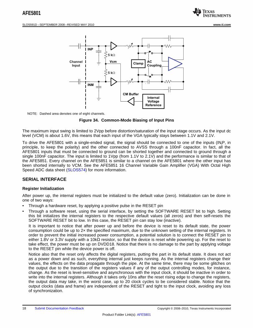
INPUT CONFIGURATION
The analog input for the AFE5801, Figure 34, consists of a differential analog buffer which has inputs biased to1.6V (usually refered as common-mode voltage, VCM). The biasing is done with two internal resistors of 5kΩ. Forproper operation, the input signal should be either ac-coupled or have a commn-mode value equal to VCM. In thecase of ac coupling, the external input capacitors form a high-pass filter with the internal bias resistors (5kΩ), so,the value of the capacitors should allow the lowest frequency of interest to pass with minimum attenuation. Forthe typical frequencies used in ultrasound (>1MHz) a value of 10nF or bigger is recommended. If dc coupling ispreferred, the user can tap the VCM output pins to set the common-mode level of the input signal. The VCM outputshould be connected to high-input-impedance circuits, as its driving capability is limited. Regardless of thechoosen input configuration, a capacitor of 100nF should be connected on each VCM input to AVSS.
For proper operation, the input signal should be in the recommended input range. The maximum input swing islimited to 2Vpp before saturation/distortion fo the input stage occurs. As the input common mode (VCM) is about1.6V, each input of the buffer should stay between 1.1V and 2.1V.
Copyright © 2008–2010, Texas Instruments Incorporated Submit Documentation Feedback 17
Product Folder Link(s): AFE5801
INP
VcmClamp
ACCoupling
InternalVoltage
Reference
CM Buffer
5 kW
5 kW
INM
ChannelInput
AFE5801
SLOS591D –SEPTEMBER 2008–REVISED MAY 2010 www.ti.com
NOTE: Dashed area denotes one of eight channels.
Figure 34. Common-Mode Biasing of Input Pins
The maximum input swing is limited to 2Vpp before distortion/saturation of the input stage occurs. As the input dclevel (VCM) is about 1.6V, this means that each input of the VGA typically stays between 1.1V and 2.1V.
To drive the AFE5801 with a single-ended signal, the signal should be connected to one of the inputs (INiP, inprinciple, to keep the polarity) and the other connected to AVSS through a 100nF capacitor. In fact, all theAFE5801 inputs that must be connected to ground can be shorted together and connected to ground through asingle 100nF capacitor. The input is limited to 1Vpp (from 1.1V to 2.1V) and the performance is similar to that ofthe AFE5851. Every channel on the AFE5851 is similar to a channel on the AFE5801 where the other input hasbeen shorted internally to VCM. See the AFE5851 16 Channel Variable Gain Amplifier (VGA) With Octal HighSpeed ADC data sheet (SLOS574) for more information.
SERIAL INTERFACE
Register Initialization
After power up, the internal registers must be initialized to the default value (zero). Initialization can be done inone of two ways:• Through a hardware reset, by applying a positive pulse in the RESET pin• Through a software reset, using the serial interface, by setting the SOFTWARE RESET bit to high. Setting
this bit initializes the internal registers to the respective default values (all zeros) and then self-resets theSOFTWARE RESET bit to low. In this case, the RESET pin can stay low (inactive).It is important to notice that after power up and before the device is reset to its default state, the powerconsumption could be up to 2× the specified maximum, due to the unknown setting of the internal registers. Inorder to prevent the initial increased power consumption, a potential solution is to connect the RESET pin toeither 1.8V or 3.3V supply with a 10kΩ resistor, so that the device is reset while powering up. For the reset totake effect, the power must be up on DVDD18. Notice that there is no damage to the part by applying voltageto the RESET pin while the device power is off.Notice also that the reset only affects the digital registers, putting the part in its default state. It does not actas a power down and as such, everything internal just keeps running. As the internal registers change theirvalues, the effects on the data propagate through the pipe. At the same time, there may be some glitches onthe output due to the transition of the registers values if any of the output controlling modes, for instance,change. As the reset is level-sensitive and asynchronous with the input clock, it should be inactive in order towrite into the internal registers. Although it takes only 10ns after the reset rising edge to change the registers,the output data may take, in the worst case, up to 20 clock cycles to be considered stable. Notice that theoutput clocks (data and frame) are independent of the RESET and tight to the input clock, avoiding any lossof synchronization.
18 Submit Documentation Feedback Copyright © 2008–2010, Texas Instruments Incorporated
Product Folder Link(s): AFE5801

T0108-04
t1
t3
t2
Power SupplyAVDD, LVDD
RESET
SEN
AFE5801
www.ti.com SLOS591D –SEPTEMBER 2008–REVISED MAY 2010
Reset Timing
Typical values at 25°C, min and max values across the full temperature range TMIN = –40°C to TMAX = 85°C,AVDD3 = 3.3V, AVDD18 = DVDD18 = 1.8V, unless otherwise noted.
PARAMATER CONDITIONS MIN TYP MAX UNIT
Delay from power-up of AVDD and LVDD to RESET pulset1 Power-on delay time 5 msactive
t2 Reset pulse width Pulse width of active RESET signal 10 ns
t3 Register write delay time Delay from RESET disable to SEN active 25 ns
tPO Power-up delay time Delay from power-up of AVDD and LVDD to output stable 6.5 ms
Figure 35. Reset Timing
Programming of different modes can be done through the serial interface formed by pins SEN (serial interfaceenable), SCLK (serial interface clock), SDATA (serial interface data) and RESET. SCLK and SDATA have a100kΩ pulldown resistor to ground, and SEN has a 100kΩ pullup resistor to DVDD18. Serial shift of bits into thedevice is enabled when SEN is low. Serial data SDATA is latched at every rising edge of SCLK when SEN isactive (low). The serial data is loaded into the register at every 24th SCLK rising edge when SEN is low. In casethe word length exceeds a multiple of 24 bits, the excess bits are ignored. Data can be loaded in multiples of24bit words within a single active SEN pulse (there is an internal counter that counts groups of 24 clocks afterthe falling edge of SEN). The interface can work with SCLK frequency from 20MHz down to very low speeds (afew Hertz) and even with a non-50% duty-cycle SCLK.
The data is divided in two main portions: a register address (8 bits) and the data itself, to load on the addressedregister (16 bits). When writing to a register with unused bits, these should be set to 0. Also, when writing, theSDOUT signal outputs zeros. The following timing diagram illustrates this process.
Copyright © 2008–2010, Texas Instruments Incorporated Submit Documentation Feedback 19
Product Folder Link(s): AFE5801

D15 D14 D13 D12 D11 D10 D9 D8 D7 D6 D5 D4 D3 D2 D1 D0A7 A6 A5 A4 A3 A2 A1 A0
SEN
SCLK
SDATA
RESET
Data Latched On Rising Edge of SCLK
Start Sequence
Start Sequence
End Sequence
End Sequence
t7
t6
t2
t4
t1
t5
t3
T0384-01
AFE5801
SLOS591D –SEPTEMBER 2008–REVISED MAY 2010 www.ti.com
Figure 36. Serial Interface Register Write
Minimum values across full temperature range TMIN = –40°C to TMAX = 85°C, AVDD3 = 3.3V, AVDD18 =DVDD18 = 1.8V.
PARAMETER DESCRIPTION MIN TYP MAX UNIT
t1 SCLK period 50 ns
t2 SCLK high time 20 ns
t3 SCLK low time 20 ns
t4 Data setup time 5 ns
t5 Data hold time 5 ns
t6 SEN fall to SCLK rise 8 ns
t7 Time between last SCLK rising edge to SEN rising edge 8 ns
GENERAL-PURPOSE REGISTER MAP
The internal registers can be divided in two groups, a group of registers to control all the general functions andsettings of the device, and a bank of registers to control the TGC/gain curves operation. Those two sets ofregisters overlap in all the address space, except for the address 0, which holds the control of the register bank.One of the bits of this register, TGC_REG_WREN (see following table) is used to access one set of registers orthe other. Its default value is zero and gives access to the general-purpose registers (which are also by defaultzero). The TGC control registers (described after the general-purpose registers) can be accessed by writing 1 toTGC_REG_WREN.
The following table describes the function of the registers when TGC_REGISTER_WREN = 0 (default). Theaddress format is address[bit of the register].
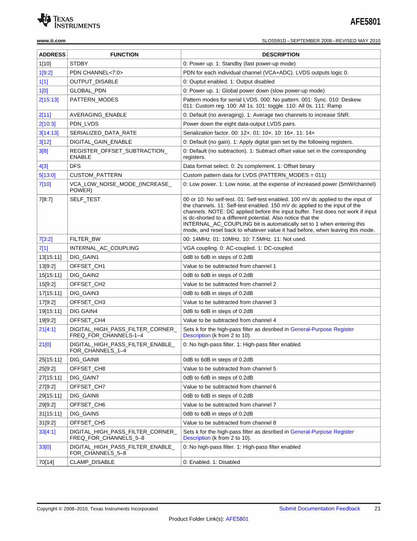
ADDRESS FUNCTION DESCRIPTION
0[2] TGC_REGISTER_WREN 0: Access to general-purpose registers. 1: Access to TGC registers
0[1] REGISTER_READOUT_ENABLE 1: Enables readout of the registers
0[0] SOFTWARE_RESET 1: Resets the device and self-resets the bit to zero
1[14] OUTPUT_RATE_2X 0: 1× rate (one ADC per LVDS stream). 1: 2× rate (2 ADCs per LVDS stream)
1[13] EXTERNAL_REFERENCE 0: Internal reference. 1: External reference
1[11] LOW_FREQUENCY_NOISE_SUPRESSION 0: No supression. 1: Supresses noise at low frequencies and pushes it to fS/2
20 Submit Documentation Feedback Copyright © 2008–2010, Texas Instruments Incorporated
Product Folder Link(s): AFE5801
AFE5801
www.ti.com SLOS591D –SEPTEMBER 2008–REVISED MAY 2010
ADDRESS FUNCTION DESCRIPTION
1[10] STDBY 0: Power up. 1: Standby (fast power-up mode)
1[9:2] PDN CHANNEL<7:0> PDN for each individual channel (VCA+ADC). LVDS outputs logic 0.
1[1] OUTPUT_DISABLE 0: Ouptut enabled. 1: Output disabled
1[0] GLOBAL_PDN 0: Power up. 1: Global power down (slow power-up mode)
2[15:13] PATTERN_MODES Pattern modes for serial LVDS. 000: No pattern. 001: Sync. 010: Deskew.011: Custom reg. 100: All 1s. 101: toggle. 110: All 0s. 111: Ramp
2[11] AVERAGING_ENABLE 0: Default (no averaging). 1: Average two channels to increase SNR.
2[10:3] PDN_LVDS Power down the eight data-output LVDS pairs.
3[14:13] SERIALIZED_DATA_RATE Serialization factor. 00: 12×. 01: 10×. 10: 16×. 11: 14×
3[12] DIGITAL_GAIN_ENABLE 0: Default (no gain). 1: Apply digital gain set by the following registers.
3[8] REGISTER_OFFSET_SUBTRACTION_ 0: Default (no subtraction). 1: Subtract offset value set in the correspondingENABLE registers.
4[3] DFS Data format select. 0: 2s complement. 1: Offset binary
5[13:0] CUSTOM_PATTERN Custom pattern data for LVDS (PATTERN_MODES = 011)
7[10] VCA_LOW_NOISE_MODE_(INCREASE_ 0: Low power. 1: Low noise, at the expense of increased power (5mW/channel)POWER)
7[8:7] SELF_TEST 00 or 10: No self-test. 01: Self-test enabled. 100 mV dc applied to the input ofthe channels. 11: Self-test enabled. 150 mV dc applied to the input of thechannels. NOTE: DC applied before the input buffer. Test does not work if inputis dc-shorted to a different potential. Also notice that theINTERNAL_AC_COUPLING bit is automatically set to 1 when entering thismode, and reset back to whatever value it had before, when leaving this mode.
7[3:2] FILTER_BW 00: 14MHz. 01: 10MHz. 10: 7.5MHz. 11: Not used.
7[1] INTERNAL_AC_COUPLING VGA coupling. 0: AC-coupled. 1: DC-coupled
13[15:11] DIG_GAIN1 0dB to 6dB in steps of 0.2dB
13[9:2] OFFSET_CH1 Value to be subtracted from channel 1
15[15:11] DIG_GAIN2 0dB to 6dB in steps of 0.2dB
15[9:2] OFFSET_CH2 Value to be subtracted from channel 2
17[15:11] DIG_GAIN3 0dB to 6dB in steps of 0.2dB
17[9:2] OFFSET_CH3 Value to be subtracted from channel 3
19[15:11] DIG GAIN4 0dB to 6dB in steps of 0.2dB
19[9:2] OFFSET_CH4 Value to be subtracted from channel 4
21[4:1] DIGITAL_HIGH_PASS_FILTER_CORNER_ Sets k for the high-pass filter as desribed in General-Purpose RegisterFREQ_FOR_CHANNELS-1–4 Description (k from 2 to 10).
21[0] DIGITAL_HIGH_PASS_FILTER_ENABLE_ 0: No high-pass filter. 1: High-pass filter enabledFOR_CHANNELS_1–4
25[15:11] DIG_GAIN8 0dB to 6dB in steps of 0.2dB
25[9:2] OFFSET_CH8 Value to be subtracted from channel 5
27[15:11] DIG_GAIN7 0dB to 6dB in steps of 0.2dB
27[9:2] OFFSET_CH7 Value to be subtracted from channel 6
29[15:11] DIG_GAIN6 0dB to 6dB in steps of 0.2dB
29[9:2] OFFSET_CH6 Value to be subtracted from channel 7
31[15:11] DIG_GAIN5 0dB to 6dB in steps of 0.2dB
31[9:2] OFFSET_CH5 Value to be subtracted from channel 8
33[4:1] DIGITAL_HIGH_PASS_FILTER_CORNER_ Sets k for the high-pass filter as desribed in General-Purpose RegisterFREQ_FOR_CHANNELS_5–8 Description (k from 2 to 10).
33[0] DIGITAL_HIGH_PASS_FILTER_ENABLE_ 0: No high-pass filter. 1: High-pass filter enabledFOR_CHANNELS_5–8
70[14] CLAMP_DISABLE 0: Enabled. 1: Disabled
Copyright © 2008–2010, Texas Instruments Incorporated Submit Documentation Feedback 21
Product Folder Link(s): AFE5801
AFE5801
SLOS591D –SEPTEMBER 2008–REVISED MAY 2010 www.ti.com
GENERAL-PURPOSE REGISTER DESCRIPTION
AVERAGING_ENABLE
Address: 2[11]When set to 1, two samples, corresponding to two consecutive channels, are averaged (channel 1 with 2, 3with 4, 5 with 6, and 7 with 8). If both channels receive the same input, the net effect is an improvement inSNR. The averaging is performed as:• Channel 1 + channel 2 comes out on channel 3.• Channel 3 + channel 4 comes out on channel 4.• Channel 5 + channel 6 comes out on channel 5.• Channel 7 + channel 8 comes out on channel 6.
DFS
Address: 4[3]DFS stands for data format select. The ADC output, by default, is in 2s-complement mode. Programming theDFS bit to 1 inverts the MSB, and the output becomes straight-offset binary mode.
DIGITAL_GAIN_ENABLE
Address: 3[12]Setting this bit to 1 applies to each channel i the corresponding gain given by DIG_GAINi<15:11>. The gainis given as 0dB + 0.2dB × DIG_GAINi<15:11>. For instance, if DIG_GAIN5<15:11> = 3, channel 5 isincreased by 0.6dB gain. DIG_GAINi<15:11> = 31 produces the same effect as DIG_GAINi<15:11> = 30,setting the gain of channel i to 6dB.
DIGITAL_HIGH_PASS_FILTER_ENABLE and DIGITAL_HIGH_PASS_FILTER_CORNER_FREQ
DIGITAL_HIGH_PASS_FILTER_ENABLE (channels 1–4): Address: 21[0]DIGITAL_HIGH_PASS_FILTER_ENABLE (channels 5–8): Address: 33[0]DIGITAL_HIGH_PASS_FILTER_CORNER_FREQ (channels 1–4): Address: 21[4:1]DIGITAL_HIGH_PASS_FILTER_CORNER_FREQ (channels 5–8): Address: 33[4:1]This group of four registers controls the characteristics of a digital high-pass transfer function applied to theoutput data, following the formula: y(n) = 2k/(2k + 1) [x(n) – x(n – 1) + y(n – 1)]. TheDIGITAL_HIGH_PASS_FILTER_CORNER_FREQ registers (one for the first four channels and one for thesecond group of four channels) describe the setting of k.
EXTERNAL_REFERENCE
Address: 1[13]The internal reference mode (default) uses approximately 3mW more power on AVDD (which is alreadyincluded in all the specification tables). The AFE5801 can operate in external reference mode byprogramming EXTERNAL_REFERENCE to 1. In this mode, the VREF_IN pin should be driven with 1.4V.Due to the high input impedace of this pin, no special drive capabilities are required. For the same reason,no decoupling on VREF_IN is needed, although depending on the noise on the 1.4V signal, some filteringmay be required. Nevertheless, when using the internal reference, there is no need to decouple VREF_IN.The advantage of using the external reference mode is that multiple AFE5801 units can be made to operatewith the same external reference, thereby improving parameters such as gain matching across devices.
FILTER_BW
Address: 7[3:2]This bit sets the 3dB attenuation frequency for the antialiasing filter (AAF).
GLOBAL_PDN
Address: 1[0]The global PDN bit is ORed with the signal in the external PDN pin (59). Therefore, a 1 on this bit shuts thedevice down completely.
22 Submit Documentation Feedback Copyright © 2008–2010, Texas Instruments Incorporated
Product Folder Link(s): AFE5801
AFE5801
www.ti.com SLOS591D –SEPTEMBER 2008–REVISED MAY 2010
INTERNAL_AC_COUPLING
Address: 7[1]This bit controls an internal high-pass filter (Figure 34), set between the input buffer and the VCA. This filterremoves the input offset to avoid its amplification by the TGC. An alternative method is to remove the offseteffect on the digital domain, either on the device following the ADC or at the ADC output, by using theDIGITAL HIGH PASS FILTER registers described previously.
LOW_FREQUENCY_NOISE_SUPPRESSION
Address: 1[11]The low-frequency noise-suppression mode is specifically useful in applications where good noiseperformance is desired in the frequency band of 0MHz to 1MHz (around dc). Setting this mode shifts thelow-frequency noise of the ADC in the AFE5801 to approximately fS/2, thereby reducing the noise flooraround dc to a much lower value.
OUTPUT_DISABLE
Address: 1[1]A 1 on this bit sets all the LVDS outputs into the high-impedance state.
OUTPUT_RATE_2X
Address: 1[14]The output data always uses a DDR format, with valid/different bits on the positive as well as the negativeedges of the LVDS bit clock, DCLK. The output rate is set by default to 1× (OUTPUT_RATE_2X = 0), whereeach ADC has one LVDS stream associated with it. If the sampling rate is low enough, two ADCs can shareone LVDS stream, in this way lowering the power consumption devoted to the interface. The unused outputswill output zero. To avoid consumption from those outputs, no termination should be connected to them. Thedistribution on the used output pairs is done in the following way:• Channel 1 and channel 2 come out on channel 3. Channel 1 comes out first.• Channel 3 and channel 4 come out on channel 4. Channel 3 comes out first.• Channel 5 and channel 6 come out on channel 5. Channel 5 comes out first.• Channel 7 and channel 8 come out on channel 6. Channel 7 comes out first.
Copyright © 2008–2010, Texas Instruments Incorporated Submit Documentation Feedback 23
Product Folder Link(s): AFE5801
AFE5801
SLOS591D –SEPTEMBER 2008–REVISED MAY 2010 www.ti.com
PATTERN_MODES and CUSTOM_PATTERN
PATTERN_MODES: Address: 2[15:13]CUSTOM_PATTERN: Address: 5[13:0]The AFE5801 can output a variety of test patterns on the LVDS outputs. These test patterns replace thenormal ADC data output and help on debugging and synchronization, with the device reading the output ofthe ADC.• PATTERN_MODE equal to 000 is the default and disables this test mode, i.e., the output data is the
same as the ADC data.• PATTERN_MODE equal to 001 (SYNC mode) replaces the normal ADC word by a fixed 1111 1100 0000
word.• PATTERN_MODE equal to 010 sets the DESKEW mode, where the 12-bit ADC output D<11:0> is
replaced with the 0101 0101 0101 word, which creates a continuous stream of 1s and 0s in the data line.• PATTERN_MODE equal to 011 outputs a constant code set by the bits in CUSTOM_PATTERN<13:0>.
Depending on the value of SERIALIZED_DATA_RATE (see following) the output bits conform to thefollowing rules:– In the default case, where SERIALIZED_DATA_RATE is 00, for 12-bit ADC data at the output, the
CUSTOM_PATTERN<13:2> bits are used, replacing the sampled data. These bits are still controlledby the LSB-first and MSB-first modes in the same way as normal ADC data are.
– For SERIALIZED_DATA_RATE = 01, 10-bit output mode is selected, and theCUSTOM_PATTERN<13:4> bits are used.
– For SERIALIZED_DATA_RATE = 10, 16-bit output mode is selected. In this case, theCUSTOM_PATTERN<13:0> bits are used for the first 14 most-significant bits, and two 0s take theplace of the LSBs.
– For SERIALIZED_DATA_RATE = 11, 14-bit mode is selected, and the CUSTOM_PATTERN<13:0>bits take the place of the output word.
• PATTERN_MODE equal to 100 makes the output always 1, whereas setting it to 110 makes the outputalways 0.
• PATTERN_MODE equal to 101 makes the output of the device toggle between two consecutive codes.On the nth sample clock, the data is 0000 0000 0000, and on the following one (nth + 1), it is1111 1111 1111.
• PATTERN_MODE equal to 111 causes all the channels to output a repeating full-scale ramp pattern. Theramp increments from zero code to full-scale code in steps of 1 LSB every clock cycle. After hitting thefull-scale code, it returns back to the zero code and ramps again.
PDN_CHANNEL<7:0>
Address: 1[9:2]Each bit controls the power down of a channel (buffer, VCA, and ADC). For example, PDN_CHANNEL<0>powers down channel 1 and the corresponding LVDS pair becomes high-impedance. DCLK and FCLK arenot powered down. They become active if terminated with 100Ω.
PDN_LVDS
Address: 2[10:3]PDN_LVDS<7:0> selects which LVDS pairs become inactive (zero output current, i.e., high-impedancestate). The frame and clock LVDS streams are powered down only when OUTPUT_DISABLE and/orGLOBAL_PDN is set.
REGISTER_OFFSET_SUBTRACTION_ENABLE
Address: 3[8]Setting this bit to 1 enables the substraction of the value on the corresponding OFFSET_CHi<9:2> (offset forchannel i) from the ADC output. The number is specified in 2s-complement format. For example,
24 Submit Documentation Feedback Copyright © 2008–2010, Texas Instruments Incorporated
Product Folder Link(s): AFE5801

x x x x x x x x x x x x x x x xA7 A6 A5 A4 A3 A2 A1 A0
SEN
SCLK
SDATA
SDOUT
SDOUT to be Latched Externally On the Rising Edge
Start Sequence End Sequence
t7
t6
t2
t4
t1
t5
t3
T0385-01
D15 D14 D13 D12 D11 D10 D9 D8 D7 D6 D5 D4 D3 D2 D1 D0
AFE5801
www.ti.com SLOS591D –SEPTEMBER 2008–REVISED MAY 2010
OFFSET_CHi<9:2> = 0100 0000 means substract –128. For OFFSET_CHi<9:2> = 0111 1111 the effect is tosubstract 127. In effect, both addition and subtraction can be performed. Note that the the offset is appliedbefore the digital gain (see DIGITAL_GAIN_ENABLE). The whole data path is 2s-complement throughoutinternally. Only when DFS = 1 (straight binary output format) is the 2s-complement word translated into offsetbinary at the end.
REGISTER_READOUT_ENABLE
Address: 0[1]The device includes an option where the contents of the internal registers can be read back. This may beuseful as a diagnostic to verify the serial interface communication between the external controller and theAFE. First, the <REGISTER READOUT ENABLE> bit must be set to 1. Then user should initiate a serialinterface cycle specifying the address of the register (A7–A0) whose content is to be read. The data bits aredon't care. The device outputs the contents (D15–D0) of the selected register on the SDOUT pin. Theexternal controller can latch the contents at the rising edge of SCLK. To enable serial register writes, set the<REGISTER READOUT ENABLE> bit back to 0. The following timing diagram shows this operation (the timespecifications follow the same information provided on the table for a serial interface register write):
Figure 37. Serial Interface Register Read
Register readback is incorrect for address 0x97. See the INTERP_ENABLE section for details.
SERIALIZED_DATA_RATE
Address: 3[14:13]These two bits control the length of the data word, i.e., the number of DCLKs per FCLK period. It is possible,for instance, to output a 16bit data stream even with a 12bit ADC. In this case, the 4 LSBs are padded with0s. The pass from higher resolution to lower serialization is not supported, however. I.e, it is not possible toselect a 10bit stream with a 12bit ADC.
TGC_REGISTER_WREN
Address: 0[2]Set this bit to 1 to access the TGC table and 0 (default after reset) to access the general-purpose registertable. The same address may point, this way, to one bank of registers (general purpose) or to the other(TGC control). Nevertheless, observe that register 0 of the general-purpose registers is always accessible,regardless of the value of TGC_REGISTER_WREN. The TGC table starts at address 1.
Copyright © 2008–2010, Texas Instruments Incorporated Submit Documentation Feedback 25
Product Folder Link(s): AFE5801

AFE5801
SLOS591D –SEPTEMBER 2008–REVISED MAY 2010 www.ti.com
VCA_LOW_NOISE_MODE
Address: 7[10]Setting this bit to 1 reduces the equivalent input noise of the VCA to 5nv/√Hz (for a 51dB gain) at theexpense of an increased power consumption (5mW increase per channel).
TGC CONTROL REGISTER MAP
The TGC operation is described in the VGA/TGC Operation section that follows. This section describes the TGCcontrol registers which can be accessed by writing 1 to TGC_REG_WREN bit. The following table describes theregister map for all the registers involved in the TGC operation.
ADDRESS D[15:7] D[8] D[7] D[6] D[5] D[4] D[3] D[2] D[1] D[0]D[0]
0x01...0x94 REG_VALUES
0x95 START_INDEX
0x96 STOP_INDEX
INTERP_0x97 0 START_GAINENABLE
0x98 HOLD_ GAIN _TIMENOT USEDUNIFORM_SOFT_ STATIC_0x99 0 0 GAIN_ FINE_GAINSYNC PGAMODE
0x9A 0 0 COARSE_GAIN
0x9B UNIFORM_GAIN_SLOPE
REG_VALUE
Address: 0x01[8:0] to 0x94[8:0]Each of these 9 bit registers (148 of them) stores the time to stay at a given gain setting, during the gainramp. The most significant bit of each register (REG_VALUE<8>) denotes either increment or decrementgain from current gain value. The other 8 bits (REG_VALUE<7:0>) denote the time (a multiple of 8 × Tclk;Tclk being the channel sampling clock, i.e., double the period of the device input clock) for the change of thegain from the CURRENT_GAIN to CURRENT_GAIN ±1dB (depending on the REG_VALUE<8>). The fastestramp (shortest time) for this 1dB gain change is set by REG_VALUE<7:0> equal to 0x00 and it is 8 × Tclk.The slowest ramp (longest time) for this 1dB gain change is set by REG_VALUE<7:0> equal to 0xFF, and itis 255 × 8 × Tclk (see VGA operation – described later).
START_INDEX
Address: 0x95[7:0]This 8 bit register specifies/points to the first REG_VALUE register of the TGC curve (i.e., where the curvestarts) and can have values ranging from 1 to 148 (in decimal).
STOP_INDEX
Address: 0x96[7:0]This 8 bit register specifies/points to the last REG_VALUE register of the TGC curve (i.e., where the curvefinishes) and can have values ranging from 1 to 148 (in decimal).
26 Submit Documentation Feedback Copyright © 2008–2010, Texas Instruments Incorporated
Product Folder Link(s): AFE5801

AFE5801
www.ti.com SLOS591D –SEPTEMBER 2008–REVISED MAY 2010
START_GAIN
Address: 0x97[5:0]This 6 bit register specifies the start gain value from –5dB to 31dB.
START_GAIN = [–5 + REG_VALUE ] dB
REG_VALUE GAIN
0x0 –5 dB0x1 –4 dB0x24 31 dB
STOP_GAIN (Not a programmable register; it is an internally computed value.)
Case 1:
INTERP_ENABLE = 1,
STOP_GAIN = START_GAIN + (STOP_INDEX – START_INDEX) – ( 2 × Number ofdecrements) + 0.875dB.
Case 2:
INTERP_ENABLE = 0,
STOP_GAIN = START_GAIN + (STOP_INDEX – START_INDEX) – ( 2 × Number ofdecrements).
HOLD_GAIN_TIME
Address: 0x98[7:0]This 8 bit register specifies the time for holding of the STOP_GAIN, after reaching either the STOP_GAINvalue as computed in the STOP_GAIN section or the maximum/minimum gain. After this time, the TGC startsstepping down to the START_GAIN value in 1dB steps every Tclk. The STOP_GAIN value is held for thefollowing number of clocks:
HOLD_GAIN_TIME = [33 × REG_VALUE] Tclks
where Tclk is the channel sampling clock.
REG_VALUE HOLD_GAIN_TIME0x0 0 Tclks0x1 33 Tclks0xFF 8415 Tclks
Copyright © 2008–2010, Texas Instruments Incorporated Submit Documentation Feedback 27
Product Folder Link(s): AFE5801
AFE5801
SLOS591D –SEPTEMBER 2008–REVISED MAY 2010 www.ti.com
INTERP_ENABLE
Address: 0x97[7]This 8 bit register sets the ramp rate. When INTERP_ENABLE = 1, the ramp rate is 0.125dB for everynumber of clocks stored in REG_VALUE:
REG_VALUE SLOPE0x0 0.125dB per Tclk0x1 0.125dB per Tclk0x2 0.125dB per 2 × Tclk0xFF 0.125dB per 255 × Tclk
When INTERP_ENABLE = 0 the ramp rate is 1dB for every 8 times the number of clocks stored in REG_VALUE:
REG_VALUE SLOPE0x0 1dB per 8 × Tclk0x1 1dB per 8 × Tclk0x2 1dB per 16 × Tclk0xFF 1dB per 255× 8 × Tclk
NOTEReading back the address 0x97 (INTERP_ENABLE) to verify its value shows the oppositevalue of what it actually is. For instance, after setting INTERP_ENABLE to 1 in addres0x97 to enable interpolation, the bit shows as 0 when reading it back from the sameaddress (0x97). After setting INTERP_ENABLE to 0 in addres 0x97 to disableinterpolation, the bit shows as 1 when reading it back.
SOFT_SYNC
Address 0x99[5]Setting SOFT_SYNC bit to 1 enables the TGC engine to run periodically following a given TGC curve,without the need for a high pulse signal in the SYNC pin (see more details in the Soft Synchronizationsection).
UNIFORM_GAIN_MODE
Address 0x99[4]Setting this bit to 0 (default) directs the TGC engine to follow an arbitrary gain-versus-time curve. If this bit isset to 1, the gain is ramped up with a slope set by the UNIFORM_GAIN_SLOPE register. (See more detailsin the Uniform Gain Increment Mode section.)
UNIFORM_GAIN_SLOPE
Address 0x9B[7:0]See the Uniform Gain Increment Mode section.
STATIC_PGA
Address 0x99[3]Setting this bit to 1 disables the TGC engine. COARSE_GAIN and FINE_GAIN control the gain value, whichis independent of time.
28 Submit Documentation Feedback Copyright © 2008–2010, Texas Instruments Incorporated
Product Folder Link(s): AFE5801
AFE5801
www.ti.com SLOS591D –SEPTEMBER 2008–REVISED MAY 2010
COARSE_GAIN
Address 0x9A[5:0]This 6 bit register specifies the coarse gain from –5 to 31dB, in 1dB steps. Observe that only values from0x00 to 0x24, both included, are valid. Setting a value bigger than 0x24 on the COARSE_GAIN register isthe same as setting 0x24. COARSE_GAIN = [–5 + REG_VALUE ] dB
REG_VALUE GAIN0x0 –5dB0x1 –4dB0x24 31dB
FINE_GAIN
Address 0x99[2:0]This 3 bit register specifies the fine gain in steps of 0.125dB resolution, from 0dB to 0.875dB. FINE_GAIN =[0.125 × REG_VALUE ] dB
REG_VALUE GAIN0x0 0dB0x1 0.125dB0x7 0.875dB
VGA/TGC OPERATION
The gain variation of the variable gain amplifier (VGA) versus time is called the TGC function and on theAFE5801 is controlled digitally. The gain is implemented by a switched network where the switches controllingthe gain are synchronized with the ADC sampling instant to minimize glitches on the output data. The gainsetting depends on the mode of operation selected by the user. There are 3 possible modes of operation:non-uniform gain, uniform gain, and static mode. The following sections describe each in detail.
Copyright © 2008–2010, Texas Instruments Incorporated Submit Documentation Feedback 29
Product Folder Link(s): AFE5801
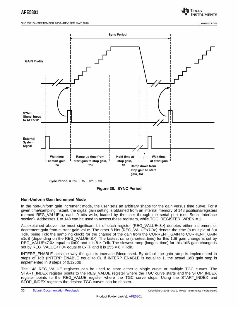
GAIN Profile
SYNC
Signal Input
to AFE5801
Hold time at
stop gain,
th Ramp down from
stop gain to start
gain, trd
Wait time
at start gain,
tw
Ramp up time from
start gain to stop gain,
tru
Wait time
at start gain
Sync Period
Sync Period = tru + th + trd + tw
External
System
Signal
AFE5801
SLOS591D –SEPTEMBER 2008–REVISED MAY 2010 www.ti.com
Figure 38. SYNC Period
Non-Uniform Gain Increment Mode
In the non-uniform gain increment mode, the user sets an arbitrary shape for the gain versus time curve. For agiven time/sampling instant, the digital gain setting is obtained from an internal memory of 148 positions/registers(named REG_VALUEs), each 9 bits wide, loaded by the user through the serial port (see Serial Interfacesection). Addresses 1 to 148 can be used to access these registers, while TGC_REGISTER_WREN = 1.
As explained above, the most significant bit of each register (REG_VALUE<8>) denotes either increment ordecrement gain from current gain value. The other 8 bits (REG_VALUE<7:0>) denote the time (a multiple of 8 ×Tclk, being Tclk the sampling clock) for the change of the gain from the CURRENT_GAIN to CURRENT_GAIN±1dB (depending on the REG_VALUE<8>). The fastest ramp (shortest time) for this 1dB gain change is set byREG_VALUE<7:0> equal to 0x00 and it is 8 × Tclk. The slowest ramp (longest time) for this 1dB gain change isset by REG_VALUE<7:0> equal to 0xFF and it is 255 × 8 × Tclk.
INTERP_ENABLE sets the way the gain is increased/decreased. By default the gain ramp is implemented insteps of 1dB (INTERP_ENABLE equal to 0). If INTERP_ENABLE is equal to 1, the actual 1dB gain step isimplemented in 8 steps of 0.125dB.
The 148 REG_VALUE registers can be used to store either a single curve or multiple TGC curves. TheSTART_INDEX register points to the REG_VALUE register where the TGC curve starts and the STOP_INDEXregister points to the REG_VALUE register where the TGC curve stops. Using the START_INDEX andSTOP_INDEX registers the desired TGC curves can be chosen.
30 Submit Documentation Feedback Copyright © 2008–2010, Texas Instruments Incorporated
Product Folder Link(s): AFE5801

AFE5801
www.ti.com SLOS591D –SEPTEMBER 2008–REVISED MAY 2010
As shown in Figure 38, a pulse high signal on the SYNC pin will set the starting gain value of the TGC curve tothe START_GAIN register value, and it will initiate the progression through the different REG_VALUEs, startingat START_INDEX. Observe that there is no option to delay the start of gain stepping after the SYNC pulse isreceived. Then, the progression continues until either the STOP_INDEX is reached or maximum/minimum gain isexceeded. After that, the last valid value of gain is held for an extra given number of clocks set by the registerHOLD_GAIN_TIME.
After the elapsing of clocks mentioned by the HOLD_GAIN_TIME register, the TGC starts to step down (or up) tothe START_GAIN in steps of 1dB every Tclk (channel sampling clock) in preparation for the next TGC profile.The TGC will start updating/following the REG_VALUEs again after a new high pulse on the SYNC pin is given.
The SYNC signal is latched by the rising edge of the channel sampling clock. In other words, the gain incrementsat the rising edge of the channel sampling clock. Setup time with rising edge is 7ns, and hold time 4ns.
Soft Synchronization
The TGC can run periodically following a given TGC curve but without the need for a high pulse signal in theSYNC pin. This is done by setting SOFT_SYNC bit to 1. Once this bit is set, the sequence of events is the sameas with the hardwired SYNC pulse. The TGC curve updates from START_INDEX to STOP_INDEX. Afterreaching STOP_INDEX or the maximum/minimum gain, the STOP_GAIN value is held for HOLD_VALUE_TIMEand then the gain ramps up or down to START_GAIN. After this the TGC update starts again automatically andrepeats all these steps periodically till the SOFT_SYNC bit becomes zero.
The SYNC process through register write occurs at the serial clock edge where the register is written. If serialclock and sample clock (channel sampling clock) are synchronous then the described relation in the hardwiredSYNC section will hold and the SYNC bit is latched by the rising edge of the channel sampling clock, respectinga setup time with rising edge of 7ns and hold time of 4ns. If sample clock and serial clock are not synchronousthen this relationship does not apply and a clock uncertainty of ±1 sample will apply in respect to the nearestsample clock rising edge.
Example 1: In the following example of non-uniform gain mode, all the 148 registers are loaded. Nevertheless,the start address for the TGC is set in START_INDEX to 2 and the stop address (STOP_INDEX) to 7. TheSTART_GAIN is set to 6 and HOLD_GAIN_TIME is 4.
With a high pulse on the SYNC pin the gain starts from 1dB (START_GAIN = 0x06). 1dB to 2dB ramp is done in120Tclks, using eight 0.125dB steps (as INTERP_ENABLE is set to 1), each 15Tclks long. The ramp from 2dB to3dB is done in 64Tclks, also in 0.125dB steps. The ramp from 3dB to 4dB is done in 40 Tclks. Decrement from4dB to 3dB in 64Tclks. Gain increment from 3dB to 4dB in 56 Tclks and from 4dB to 4.875dB in 80 Tclks.
Observe that in the case where INTERP_ENABLE = 1, STOP_GAIN = START_GAIN + (STOP_INDEX –START_INDEX) – ( 2 × Number of decrements) + 0.875dB. In the case where INTERP_ENABLE = 0,STOP_GAIN = START_GAIN + (STOP_INDEX – START_INDEX) – ( 2 × Number of Decrements). This is due tothe fact that the interpolation engine keeps the gain increasing or decreasing when INTERP_ENABLE = 1, whilethe gain is frozen when INTERP_ENABLE = 0.
TGC REG INDEX REG_VALUE[8:0] Number of Tclks Direction of Gain Change
1 0x004 4 × 8 = 32 Increment
2 0x00F 15 × 8 = 120 Increment
3 0x008 8 × 8 = 64 Increment
4 0x005 5 × 8 40 Increment
5 0x108 8 × 8 = 64 Decrement
6 0x007 7 × 8 = 56 Increment
7 0x00A 10 × 8 = 80 Increment
... ... ... ...
147 0x00F 15 × 8 = 120 Increment
148 0x00F 15 × 8 = 120 Increment
Copyright © 2008–2010, Texas Instruments Incorporated Submit Documentation Feedback 31
Product Folder Link(s): AFE5801
AFE5801
SLOS591D –SEPTEMBER 2008–REVISED MAY 2010 www.ti.com
NAME VALUE
START_INDEX 0x02
STOP_INDEX 0x07
START_GAIN 0x06
HOLD_GAIN_TIME 0x04
INTERP_ENABLE 1
UNIFORM_GAIN_MODE 0
Uniform Gain Increment Mode
By setting UNIFORM_GAIN_MODE to 1, the TGC engine can also be configured for a uniform increment gainramp mode where the gain is ramped up from the START_GAIN value to the STOP_GAIN with a slope set bythe UNIFORM_GAIN_SLOPE register. Note: STOP_GAIN is not a programmable register, but just an internallycomputed value from START_GAIN, UNIFORM_GAIN_SLOPE, START_INDEX and STOP_INDEX.
If INTERP_ENABLE = 1, UNIFORM_GAIN_SLOPE sets the number of Tclk (channel sampling clock) at a givengain before incrementing or decrementing 0.125dB. If INTERP_ENABLE = 0, this register sets the number of 8 ×Tclk (eight sampling periods) at a given gain before incrementing or decrementing 1dB. Observe that in bothcases the time it takes to step by 1dB is the same. In INTERP_ENABLE = 0 the gain is stationary at the samesetting for the given time, whereas in the other case the gain increments in fine gain steps of 0.125dB to coverthat 1dB step
When INTERP_ENABLE is zero, the STOP_GAIN is computed as START_GAIN +(STOP_INDEX-START_INDEX). Nevertheless, when INTERP_ENABLE = 1, the STOP_GAIN is equal toSTART_GAIN + (STOP_INDEX - START_INDEX) + 0.875dB. This is basically due to the fact that theinterpolation engine keeps the gain increasing on the second case, while, as explained above, is frozen on thefirst case. Observe that START_INDEX and STOP_INDEX are not used in this case as pointers to theREG_VALUEs table. Instead, only the difference between the two is important to compute STOP_GAIN. Assuch, START_INDEX can be set to zero and STOP_INDEX will store STOP_GAIN – START_GAIN. Observethat only positive slope ramps are possible.
Example 1: setting START_GAIN = 0x2 (–3dB), START_INDEX = 0x00, STOP_INDEX = 0x06,INTERP_ENABLE = 0 and UNIFORM_GAIN_SLOPE = 0x8, will set the gain at –3dB for 8 × 8 × Tclk, then to–2dB for another 64 Tclk, and so on, through –1, 0, 1, 2 and 3. After spending 64 × Tclk in 3dB, the gain will stayat that gain setting for HOLD_GAIN_TIME and start stepping down back to START_GAIN, with 1dB per Tclk.
Example 2: for the same settings, START_GAIN = 0x2 (–3dB), START_INDEX = 0x00, STOP_INDEX = 0x06,and UNIFORM_GAIN_SLOPE = 0x8, if we set INTERP_ENABLE = 1, the gain will start at –3dB for 8Tclk, then–2.875dB for another 8Tclk, then –2.750dB and so on, till 3dB. At this point, while in example 1, withINTERP_ENABLE = 0 the gain would be frozen for another 64 Tclk, in this example, the gain will continue toincrease with 0.125dB steps every 8Tclk till 3.875dB is reached. There will stay for another 8Tclk before startingto wait for HOLD_GAIN_TIME and start stepping down.
Example 3: for START_GAIN = 0x2 (–3dB) , START_INDEX = 0x00, STOP_INDEX = 0x00, INTERP_ENABLE =1 and UNIFORM_GAIN_SLOPE = 0x1, the gain will step through –3dB, –2.875, –2.75, –2.625, –2.5, –2.375,–2.25 and –2.125, staying at each of these 8 values 1 clock cycle (8 total). Then it will wait forHOLD_GAIN_TIME in –2.125dB and then it will start stepping down back to –3dB.
Example 4: same settings as example 3, but with INTERP_ENABLE = 0, would simply set the VGA gain to –3dBfor 8 clock cycles and then the logic would wait for HOLD_GAIN_TIME.
Static PGA Mode
The 3rd mode of operation is actually a mode where the TGC engine is disabled by writing 1 into theSTATIC_PGA bit. This enables the use of a fixed gain mode where the gain is obtained by the sum of a coarseand a fine gain. Coarse gain can be set from –5 to 31dB, in 1dB steps, by the register COARSE_GAIN (6 bitword from 0x00 to 0x24). Setting a value bigger than 0x24 on the COARSE_GAIN register is the same as setting0x24. The fine gain can be set in steps of 0.125dB resolution, from 0dB to 0.875dB by the FINE_GAIN register (3bit word with range from 0x00 to 0x07). Observe that the maximum gain, when both registers are set to theirmaximum gains, is actually 31.875dB.
32 Submit Documentation Feedback Copyright © 2008–2010, Texas Instruments Incorporated
Product Folder Link(s): AFE5801
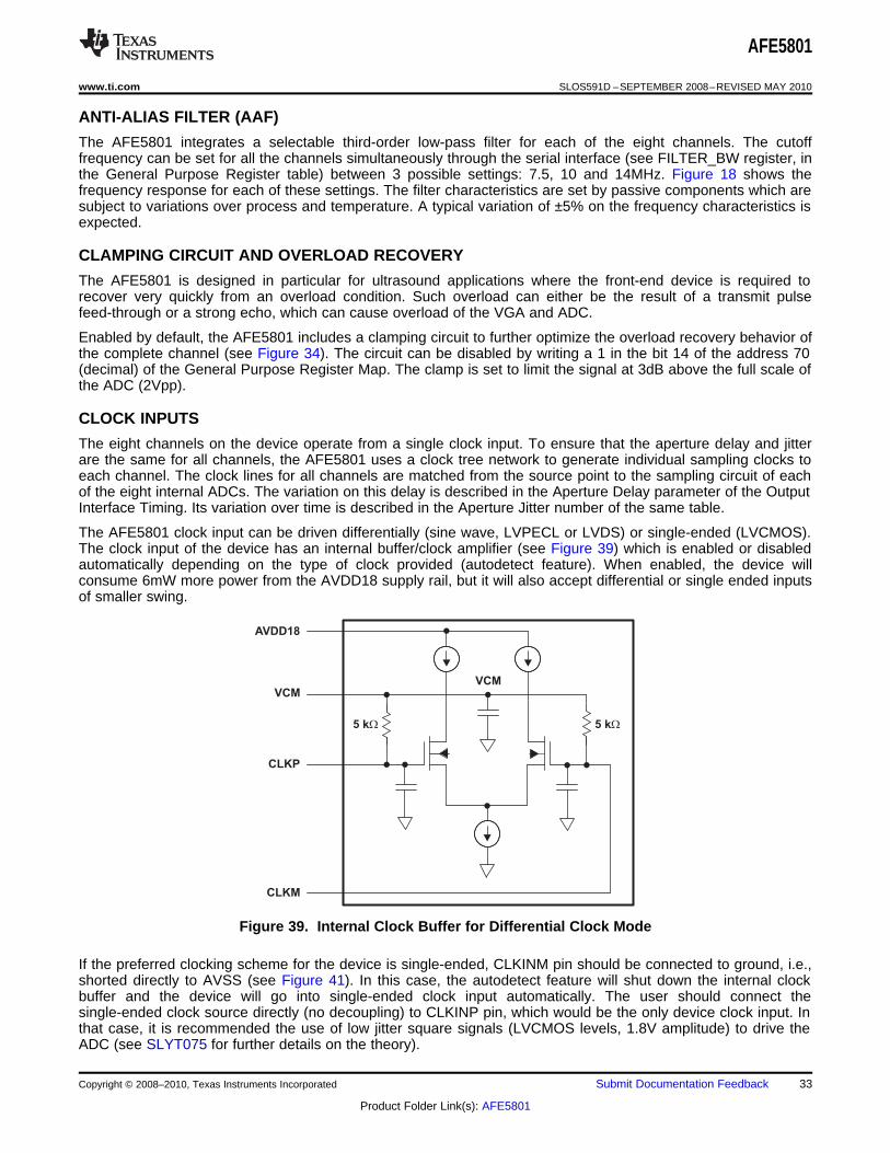
VCM
CLKP
CLKM
5 kW 5 kW
VCM
AVDD18
AFE5801
www.ti.com SLOS591D –SEPTEMBER 2008–REVISED MAY 2010
ANTI-ALIAS FILTER (AAF)
The AFE5801 integrates a selectable third-order low-pass filter for each of the eight channels. The cutofffrequency can be set for all the channels simultaneously through the serial interface (see FILTER_BW register, inthe General Purpose Register table) between 3 possible settings: 7.5, 10 and 14MHz. Figure 18 shows thefrequency response for each of these settings. The filter characteristics are set by passive components which aresubject to variations over process and temperature. A typical variation of ±5% on the frequency characteristics isexpected.
CLAMPING CIRCUIT AND OVERLOAD RECOVERY
The AFE5801 is designed in particular for ultrasound applications where the front-end device is required torecover very quickly from an overload condition. Such overload can either be the result of a transmit pulsefeed-through or a strong echo, which can cause overload of the VGA and ADC.
Enabled by default, the AFE5801 includes a clamping circuit to further optimize the overload recovery behavior ofthe complete channel (see Figure 34). The circuit can be disabled by writing a 1 in the bit 14 of the address 70(decimal) of the General Purpose Register Map. The clamp is set to limit the signal at 3dB above the full scale ofthe ADC (2Vpp).
CLOCK INPUTS
The eight channels on the device operate from a single clock input. To ensure that the aperture delay and jitterare the same for all channels, the AFE5801 uses a clock tree network to generate individual sampling clocks toeach channel. The clock lines for all channels are matched from the source point to the sampling circuit of eachof the eight internal ADCs. The variation on this delay is described in the Aperture Delay parameter of the OutputInterface Timing. Its variation over time is described in the Aperture Jitter number of the same table.
The AFE5801 clock input can be driven differentially (sine wave, LVPECL or LVDS) or single-ended (LVCMOS).The clock input of the device has an internal buffer/clock amplifier (see Figure 39) which is enabled or disabledautomatically depending on the type of clock provided (autodetect feature). When enabled, the device willconsume 6mW more power from the AVDD18 supply rail, but it will also accept differential or single ended inputsof smaller swing.
Figure 39. Internal Clock Buffer for Differential Clock Mode
If the preferred clocking scheme for the device is single-ended, CLKINM pin should be connected to ground, i.e.,shorted directly to AVSS (see Figure 41). In this case, the autodetect feature will shut down the internal clockbuffer and the device will go into single-ended clock input automatically. The user should connect thesingle-ended clock source directly (no decoupling) to CLKINP pin, which would be the only device clock input. Inthat case, it is recommended the use of low jitter square signals (LVCMOS levels, 1.8V amplitude) to drive theADC (see SLYT075 for further details on the theory).
Copyright © 2008–2010, Texas Instruments Incorporated Submit Documentation Feedback 33
Product Folder Link(s): AFE5801
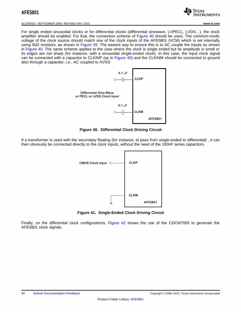
AFE5851
0.1 Fm
0.1 Fm
CLKP
CLKM
AFE5801
Differential Sine-Wave
or PECL or LVDS Clock Input
AFE5851
CLKP
CLKM
AFE5801
CMOS Clock Input
AFE5801
SLOS591D –SEPTEMBER 2008–REVISED MAY 2010 www.ti.com
For single ended sinusoidal clocks or for differential clocks (differential sinewave, LVPECL, LVDS…), the clockamplifier should be enabled. For that, the connection scheme of Figure 40 should be used. The common-modevoltage of the clock source should match one of the clock inputs of the AFE5801 (VCM) which is set internallyusing 5kΩ resistors, as shown in Figure 39. The easiest way to ensure this is to AC couple the inputs as shownin Figure 40. The same scheme applies to the case where the clock is single ended but its amplitude is small orits edges are not sharp (for instance, with a sinusoidal single-ended clock). In this case, the input clock signalcan be connected with a capacitor to CLKINP (as in Figure 40) and the CLKINM should be connected to groundalso through a capacitor, i.e., AC coupled to AVSS.
Figure 40. Differential Clock Driving Circuit
If a transformer is used with the secondary floating (for instance, to pass from single-ended to differential) , it canthen obviously be connected directly to the clock inputs, without the need of the 100nF series capacitors.
Figure 41. Single-Ended Clock Driving Circuit
Finally, on the differential clock configurations, Figure 42 shows the use of the CDCM7005 to generate theAFE5801 clock signals.
34 Submit Documentation Feedback Copyright © 2008–2010, Texas Instruments Incorporated
Product Folder Link(s): AFE5801
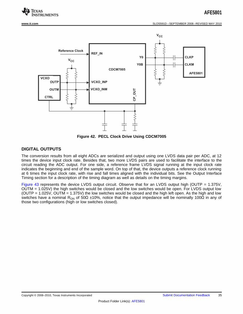
Reference Clock
VCC
REF_IN
VCXO_INP
VCXO_INM
Y0
CP
_O
UT
Y0B
VCXO
OUTP
OUTM
CTRL
CLKP
CLKM
AFE5801
VCC
CDCM7005
AFE5801
www.ti.com SLOS591D –SEPTEMBER 2008–REVISED MAY 2010
Figure 42. PECL Clock Drive Using CDCM7005
DIGITAL OUTPUTS
The conversion results from all eight ADCs are serialized and output using one LVDS data pair per ADC, at 12times the device input clock rate. Besides that, two more LVDS pairs are used to facilitate the interface to thecircuit reading the ADC output. For one side, a reference frame LVDS signal running at the input clock rateindicates the beginning and end of the sample word. On top of that, the device outputs a reference clock runningat 6 times the input clock rate, with rise and fall times aligned with the individual bits. See the Output InterfaceTiming section for a description of the timing diagram as well as details on the timing margins.
Figure 43 represents the device LVDS output circuit. Observe that for an LVDS output high (OUTP = 1.375V,OUTM = 1.025V) the high switches would be closed and the low switches would be open. For LVDS output low(OUTP = 1.025V, OUTM = 1.375V) the low switches would be closed and the high left open. As the high and lowswitches have a nominal RON of 50Ω ±10%, notice that the output impedance will be nominally 100Ω in any ofthose two configurations (high or low switches closed).
Copyright © 2008–2010, Texas Instruments Incorporated Submit Documentation Feedback 35
Product Folder Link(s): AFE5801

OUTP
OUTM
External
Switch impedance is
Nominally 50 ( ±10%)W
ROUT
+0.35 V
-0.35 V1.2 V
Hig
hL
ow
Lo
wH
igh
100 LoadW
AFE5801
SLOS591D –SEPTEMBER 2008–REVISED MAY 2010 www.ti.com
Figure 43. LVDS Output Circuit
EXTERNAL/INTERNAL REFERENCE
See EXTERNAL_REFERENCE register description in the General Purpose Register Description Section.
POWER SUPPLIES
The use of low noise power supplies with adequate decoupling is recommended, being the linear supplies thefirst choice vs switched ones, which tend to generate more noise components that can be coupled to theAFE5801.
There is no need of any type of power-up sequencing, although a positive pulse must be applied to the Reset pinonce the power supplies are considered stable (see Serial Interface Section)
There are several types of powerdown modes. On the standby mode all circuits but the reference generator arepowered-down. This enables for a fast recovery from power down to full operation. On the full power down mode,all the blocks are powered down (except some digital circuits). The power savings are bigger but the power-upwill also be slower (see specification tables for more details). The device includes also the possibility of poweringdown pairs of channels (corresponding to the same ADC) through the use of PDN_Channel<7:0> and poweringdown the LVDS outputs by using PDN_LVDS.
Finally, notice that the metallic heat sink under the package is also connected to analog ground.
LAYOUT INFORMATION
The evaluation board represents a good guideline of how to layout the board to obtain the maximumperformance out of the AFE5801. General design rules as the use of multilayer boards, single ground plane forboth, analog and digital ADC ground connections, and local decoupling ceramic chip capacitors should beapplied. The input traces should be isolated from any external source of interference or noise, including thedigital outputs as well as the clock traces. Clock should also be isolated from other signals although the lowfrequencies of the input signal relaxes the jitter requirements.
In order to maintain proper LVDS timing, all LVDS traces should follow a controlled impedance design (forexample, 100Ω differential). In addition, all LVDS trace lengths should be equal and symmetrical. It isrecommended to keep trace length variations less than 150mil (0.150in or 3.81mm).
It is necessary to solder the exposed pad at the bottom of the package to a ground plane for best thermalperformance. For detailed information, see application notes QFN Layout Guidelines (SLOA122A) and QFN/SONPCB Attachment (SLUA271A).
36 Submit Documentation Feedback Copyright © 2008–2010, Texas Instruments Incorporated
Product Folder Link(s): AFE5801

SNR 10Log10PSPN
AFE5801
www.ti.com SLOS591D –SEPTEMBER 2008–REVISED MAY 2010
DEFINITION OF SPECIFICATIONS
Analog Bandwidth – The analog input frequency at which the power of the fundamental is reduced by 3 dB withrespect to the low frequency value.
Aperture Delay –The delay in time between the rising or the falling edge of the input sampling clock (dependingon the channel) and the actual time at which the sampling occurs. This delay will be different across channels.The maximum variation is specified as aperture delay variation (channel-channel).
Aperture Uncertainty (Jitter) – The sample-to-sample variation in aperture delay.
Clock Pulse Width/Duty Cycle – The duty cycle of a clock signal is the ratio of the time the clock signal remainsat a logic high (clock pulse width) to the period of the clock signal. Duty cycle is typically expressed as apercentage. A perfect differential sine-wave clock results in a 50% duty cycle.
Maximum Conversion Rate – The maximum sampling rate at which certified operation is given. All parametrictesting is performed at this sampling rate unless otherwise noted.
Minimum Conversion Rate – The minimum sampling rate at which the ADC functions.
Differential Nonlinearity (DNL) – An ideal ADC exhibits code transitions at analog input values spaced exactly1 LSB apart. The DNL is the deviation of any single step from this ideal value, measured in units of LSBs.
Integral Nonlinearity (INL) – The INL is the deviation of the ADC's transfer function from a best fit linedetermined by a least squares curve fit of that transfer function, measured in units of LSBs.
Gain Error – The difference between the actual gain of a channel & its ideal (theoretical) gain, i.e., the error inthe absolute gain of the channel.
Gain Matching – The gain difference between two channels with same theoretical gain setting. For perfectmatching, the difference should be zero. On the context of this device, the gain matching is obtained in twodifferent ways:1. The values on the specification table represent the expected gain matching between any two channels on
the system. The gain is measured on every channel of every device, for a given gain setting, at anytemperature. The difference between the maximum recorded gain and the minimum recorded gainrepresents the gain matching at that given gain setting. The same is done for every gain setting and themaximum difference for any gain setting is presented on the table.
2. The gain matching histogram represents the channel to channel matching inside the same device, i.e., themaximum expected gain difference between any two channels of the same device, or in other words, thepeak-to-peak variation of absolute gains across all channels in the device. At a given gain setting for all thechannels of a given device (at one temperature assumed common to the whole device), the differencebetween the channel with maximum gain and the channel with minimum gain represents one count. Thesame thing is done for all the devices and for 3 temperatures (–40C, 25C and 85C). Every measurement of adevice at one given temperature represents one count.
Offset Error – The offset error is the difference, given in mV, between the ADC's actual average idle-channeloutput code and the ideal average idle-channel output code.
Temperature Drift – The temperature drift coefficient (with respect to gain error and offset error) specifies thechange per degree Celsius of the parameter from TMIN to TMAX. It is calculated by dividing the maximum deviationof the parameter across the TMIN to TMAX range by the difference TMAX – TMIN.
Signal-to-Noise Ratio – SNR is the ratio of the power of the fundamental (PS) to the noise floor power (PN),excluding the power at DC and the first nine harmonics.
(1)
SNR is either given in units of dBc (dB to carrier) when the absolute power of the fundamental is used as thereference, or dBFS (dB to full scale) when the power of the fundamental is extrapolated to the full-scaleconverter range.
Signal-to-Noise and Distortion (SINAD) – SINAD is the ratio of the power of the fundamental (PS) to the powerof all the other spectral components including noise (PN) and distortion (PD), but excluding dc.
Copyright © 2008–2010, Texas Instruments Incorporated Submit Documentation Feedback 37
Product Folder Link(s): AFE5801

S
N D
PSINAD = 10 log 10
P + P
ENOB SINAD 1.76
6.02
S
D
PTHD = 10 log 10
P
VoutPSRR = 20 log
Vsup
æ öD
ç ÷Dè ø
AFE5801
SLOS591D –SEPTEMBER 2008–REVISED MAY 2010 www.ti.com
(2)
SINAD is either given in units of dBc (dB to carrier) when the absolute power of the fundamental is used as thereference, or dBFS (dB to full scale) when the power of the fundamental is extrapolated to the full-scaleconverter range.
Effective Number of Bits (ENOB) – The ENOB is a measure the performance of a converter as compared tothe theoretical limit based on quantization noise.
(3)
Spurious-Free Dynamic Range (SFDR) – SFDR is the ratio of the power of the fundamental (PS) to the highestFFT bin, harmonic or not, excluding DC. SFDR is typically given in units of dBc (dB to carrier).
Second Harmonic Distortion (HD2) – HD2 is the ratio of the power of the fundamental (PS) to the secondharmonic, typically given in units of dBc (dB to carrier).
Third Harmonic Distortion (HD3) –HD3 is the ratio of the power of the fundamental (PS) to the third harmonic,typically given in units of dBc (dB to carrier).
Total Harmonic Distortion (THD) – THD is the ratio of the power of the fundamental (PS) to the power of thefirst nine harmonics (PD).
(4)
THD is typically given in units of dBc (dB to carrier).
AC Power Supply Rejection Ratio (AC PSRR) – A measure of the device immunity to variations in its supplyvoltage. In this datasheet, if ΔVSUP represents the change in supply voltage and ΔVOUT is the resultant changeof the ADC output code (referred to the input), then:
(5)
38 Submit Documentation Feedback Copyright © 2008–2010, Texas Instruments Incorporated
Product Folder Link(s): AFE5801
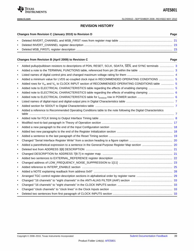
AFE5801
www.ti.com SLOS591D –SEPTEMBER 2008–REVISED MAY 2010
REVISION HISTORY
Changes from Revision C (January 2010) to Revision D Page
• Deleted INVERT_CHANNEL and MSB_FIRST rows from register map table ................................................................... 21
• Deleted INVERT_CHANNEL register description ............................................................................................................... 23
• Deleted MSB_FIRSTL register description ......................................................................................................................... 23
Changes from Revision B (April 2009) to Revision C Page
• Added pullup/pulldown resistors to descriptions of PDN, RESET, SCLK, SDATA, SEN, and SYNC terminals .................. 3
• Added a note to the TERMINAL FUNCTIONS table, referenced from pin 28 within the table ............................................ 3
• Listed names of digital control pins and changed maximum voltage rating for them ........................................................... 4
• Added a minimum value for LVDS ac-coupled clock input in RECOMMENDED OPERATING CONDITIONS ................... 5
• Added rows for VIH and VIL to CLOCK INPUT section of RECOMMENDED OPERATING CONDITIONS table ................ 5
• Added note to ELECTRICAL CHARACTERISTICS table regarding the effects of enabling clamping ................................ 5
• Added note to ELECTRICAL CHARACTERISTICS table regarding the effects of enabling clamping ................................ 6
• Added note to ELECTRICAL CHARACTERISTICS table for IDVDD18 row in POWER section .............................................. 6
• Listed names of digital-input and digital-output pins in Digital Characteristics table ............................................................ 7
• Added section for SDOUT to Digital Characteristics table ................................................................................................... 7
• Added a reference to Recommended Operating Conditions table to the note following the Digital Characteristicstable ...................................................................................................................................................................................... 7
• Added note for FCLK timing to Output Interface Timing table .............................................................................................. 8
• Modified next-to-last paragraph in Theory of Operation section ......................................................................................... 17
• Added a new paragraph to the end of the Input Configuration section .............................................................................. 18
• Added two new paragraphs to the end of the Register Initialization section ...................................................................... 18
• Added a sentence to the last paragraph of the Reset Timing section ................................................................................ 19
• Changed "Serial Interface Register Write" from a section heading to a figure caption ...................................................... 20
• Added a parenthetical expression to a sentence in the General-Purpose Register Map section ...................................... 20
• Deleted text from ADDRESS 3[8] DESCRIPTION ............................................................................................................. 21
• Changed DESCRIPTION for ADDRESS 7[8:7] in register map. ........................................................................................ 21
• Added two sentences to EXTERNAL_REFERENCE register description .......................................................................... 22
• Changed address of LOW_FREQUENCY_NOISE_SUPPRESSION to 1[11] ................................................................... 23
• Added reference to INTERP_ENABLE section .................................................................................................................. 25
• Added a NOTE explaining readback from address 0x97 ................................................................................................... 28
• Arranged TGC control register-description sections in alphabetical order by register name ............................................. 29
• Changed "16 channels" to "eight channels" in the ANTI-ALIAS FILTER (AAF) section .................................................... 33
• Changed "16 channels" to "eight channels" in the CLOCK INPUTS section ..................................................................... 33
• Changed "clock channels" to "clock lines" in the Clock Inputs section .............................................................................. 33
• Deleted two sentences from first paragraph of CLOCK INPUTS section ........................................................................... 33
Copyright © 2008–2010, Texas Instruments Incorporated Submit Documentation Feedback 39
Product Folder Link(s): AFE5801
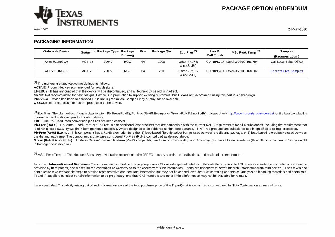
PACKAGE OPTION ADDENDUM
www.ti.com 24-May-2010
Addendum-Page 1
PACKAGING INFORMATION
Orderable Device Status (1) Package Type PackageDrawing
Pins Package Qty Eco Plan (2) Lead/Ball Finish
MSL Peak Temp (3) Samples
(Requires Login)
AFE5801IRGCR ACTIVE VQFN RGC 64 2000 Green (RoHS& no Sb/Br)
CU NIPDAU Level-3-260C-168 HR Call Local Sales Office
AFE5801IRGCT ACTIVE VQFN RGC 64 250 Green (RoHS& no Sb/Br)
CU NIPDAU Level-3-260C-168 HR Request Free Samples
(1) The marketing status values are defined as follows:ACTIVE: Product device recommended for new designs.LIFEBUY: TI has announced that the device will be discontinued, and a lifetime-buy period is in effect.NRND: Not recommended for new designs. Device is in production to support existing customers, but TI does not recommend using this part in a new design.PREVIEW: Device has been announced but is not in production. Samples may or may not be available.OBSOLETE: TI has discontinued the production of the device.
(2) Eco Plan - The planned eco-friendly classification: Pb-Free (RoHS), Pb-Free (RoHS Exempt), or Green (RoHS & no Sb/Br) - please check http://www.ti.com/productcontent for the latest availabilityinformation and additional product content details.TBD: The Pb-Free/Green conversion plan has not been defined.Pb-Free (RoHS): TI's terms "Lead-Free" or "Pb-Free" mean semiconductor products that are compatible with the current RoHS requirements for all 6 substances, including the requirement thatlead not exceed 0.1% by weight in homogeneous materials. Where designed to be soldered at high temperatures, TI Pb-Free products are suitable for use in specified lead-free processes.Pb-Free (RoHS Exempt): This component has a RoHS exemption for either 1) lead-based flip-chip solder bumps used between the die and package, or 2) lead-based die adhesive used betweenthe die and leadframe. The component is otherwise considered Pb-Free (RoHS compatible) as defined above.Green (RoHS & no Sb/Br): TI defines "Green" to mean Pb-Free (RoHS compatible), and free of Bromine (Br) and Antimony (Sb) based flame retardants (Br or Sb do not exceed 0.1% by weightin homogeneous material)
(3) MSL, Peak Temp. -- The Moisture Sensitivity Level rating according to the JEDEC industry standard classifications, and peak solder temperature.
Important Information and Disclaimer:The information provided on this page represents TI's knowledge and belief as of the date that it is provided. TI bases its knowledge and belief on informationprovided by third parties, and makes no representation or warranty as to the accuracy of such information. Efforts are underway to better integrate information from third parties. TI has taken andcontinues to take reasonable steps to provide representative and accurate information but may not have conducted destructive testing or chemical analysis on incoming materials and chemicals.TI and TI suppliers consider certain information to be proprietary, and thus CAS numbers and other limited information may not be available for release.
In no event shall TI's liability arising out of such information exceed the total purchase price of the TI part(s) at issue in this document sold by TI to Customer on an annual basis.

TAPE AND REEL INFORMATION
*All dimensions are nominal
Device PackageType
PackageDrawing
Pins SPQ ReelDiameter
(mm)
ReelWidth
W1 (mm)
A0(mm)
B0(mm)
K0(mm)
P1(mm)
W(mm)
Pin1Quadrant
AFE5801IRGCR VQFN RGC 64 2000 330.0 16.4 9.3 9.3 1.5 12.0 16.0 Q2
AFE5801IRGCT VQFN RGC 64 250 330.0 16.4 9.3 9.3 1.5 12.0 16.0 Q2
PACKAGE MATERIALS INFORMATION
www.ti.com 24-May-2010
Pack Materials-Page 1

*All dimensions are nominal
Device Package Type Package Drawing Pins SPQ Length (mm) Width (mm) Height (mm)
AFE5801IRGCR VQFN RGC 64 2000 333.2 345.9 28.6
AFE5801IRGCT VQFN RGC 64 250 333.2 345.9 28.6
PACKAGE MATERIALS INFORMATION
www.ti.com 24-May-2010
Pack Materials-Page 2

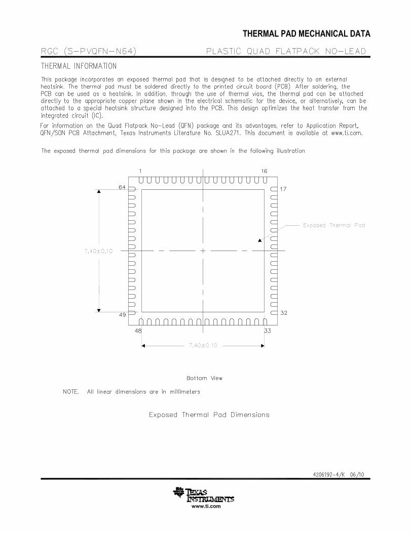
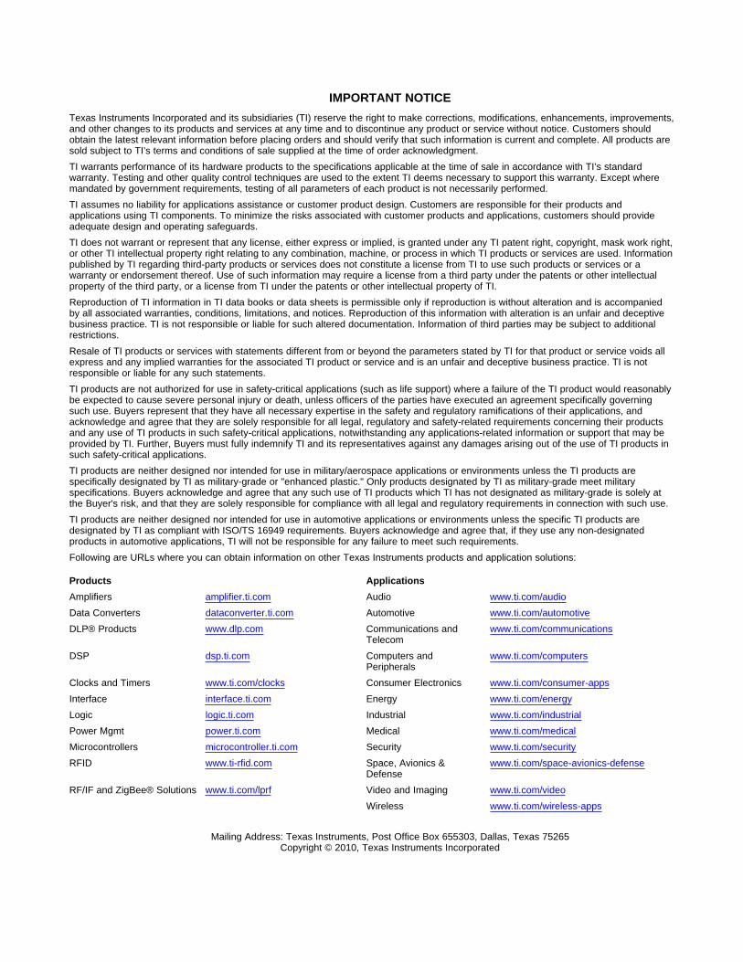
IMPORTANT NOTICE
Texas Instruments Incorporated and its subsidiaries (TI) reserve the right to make corrections, modifications, enhancements, improvements,and other changes to its products and services at any time and to discontinue any product or service without notice. Customers shouldobtain the latest relevant information before placing orders and should verify that such information is current and complete. All products aresold subject to TI’s terms and conditions of sale supplied at the time of order acknowledgment.
TI warrants performance of its hardware products to the specifications applicable at the time of sale in accordance with TI’s standardwarranty. Testing and other quality control techniques are used to the extent TI deems necessary to support this warranty. Except wheremandated by government requirements, testing of all parameters of each product is not necessarily performed.
TI assumes no liability for applications assistance or customer product design. Customers are responsible for their products andapplications using TI components. To minimize the risks associated with customer products and applications, customers should provideadequate design and operating safeguards.
TI does not warrant or represent that any license, either express or implied, is granted under any TI patent right, copyright, mask work right,or other TI intellectual property right relating to any combination, machine, or process in which TI products or services are used. Informationpublished by TI regarding third-party products or services does not constitute a license from TI to use such products or services or awarranty or endorsement thereof. Use of such information may require a license from a third party under the patents or other intellectualproperty of the third party, or a license from TI under the patents or other intellectual property of TI.
Reproduction of TI information in TI data books or data sheets is permissible only if reproduction is without alteration and is accompaniedby all associated warranties, conditions, limitations, and notices. Reproduction of this information with alteration is an unfair and deceptivebusiness practice. TI is not responsible or liable for such altered documentation. Information of third parties may be subject to additionalrestrictions.
Resale of TI products or services with statements different from or beyond the parameters stated by TI for that product or service voids allexpress and any implied warranties for the associated TI product or service and is an unfair and deceptive business practice. TI is notresponsible or liable for any such statements.
TI products are not authorized for use in safety-critical applications (such as life support) where a failure of the TI product would reasonablybe expected to cause severe personal injury or death, unless officers of the parties have executed an agreement specifically governingsuch use. Buyers represent that they have all necessary expertise in the safety and regulatory ramifications of their applications, andacknowledge and agree that they are solely responsible for all legal, regulatory and safety-related requirements concerning their productsand any use of TI products in such safety-critical applications, notwithstanding any applications-related information or support that may beprovided by TI. Further, Buyers must fully indemnify TI and its representatives against any damages arising out of the use of TI products insuch safety-critical applications.
TI products are neither designed nor intended for use in military/aerospace applications or environments unless the TI products arespecifically designated by TI as military-grade or "enhanced plastic." Only products designated by TI as military-grade meet militaryspecifications. Buyers acknowledge and agree that any such use of TI products which TI has not designated as military-grade is solely atthe Buyer's risk, and that they are solely responsible for compliance with all legal and regulatory requirements in connection with such use.
TI products are neither designed nor intended for use in automotive applications or environments unless the specific TI products aredesignated by TI as compliant with ISO/TS 16949 requirements. Buyers acknowledge and agree that, if they use any non-designatedproducts in automotive applications, TI will not be responsible for any failure to meet such requirements.
Following are URLs where you can obtain information on other Texas Instruments products and application solutions:
Products Applications
Amplifiers amplifier.ti.com Audio www.ti.com/audio
Data Converters dataconverter.ti.com Automotive www.ti.com/automotive
DLP® Products www.dlp.com Communications and www.ti.com/communicationsTelecom
DSP dsp.ti.com Computers and www.ti.com/computersPeripherals
Clocks and Timers www.ti.com/clocks Consumer Electronics www.ti.com/consumer-apps
Interface interface.ti.com Energy www.ti.com/energy
Logic logic.ti.com Industrial www.ti.com/industrial
Power Mgmt power.ti.com Medical www.ti.com/medical
Microcontrollers microcontroller.ti.com Security www.ti.com/security
RFID www.ti-rfid.com Space, Avionics & www.ti.com/space-avionics-defenseDefense
RF/IF and ZigBee® Solutions www.ti.com/lprf Video and Imaging www.ti.com/video
Wireless www.ti.com/wireless-apps
Mailing Address: Texas Instruments, Post Office Box 655303, Dallas, Texas 75265Copyright © 2010, Texas Instruments Incorporated


