ADVP-BasedBridgeArchitecturetoRandomlyAccessPixelsof High ...
13
Hindawi Publishing Corporation EURASIP Journal on Embedded Systems Volume 2011, Article ID 270908, 13 pages doi:10.1155/2011/270908 Research Article A DVP-Based Bridge Architecture to Randomly Access Pixels of High-Speed Image Sensors Tareq Hasan Khan and Khan A. Wahid Department of Electrical and Computer Engineering, University of Saskatchewan, 57 Campus Drive, Saskatoon, SK, Canada S7N 5A9 Correspondence should be addressed to Tareq Hasan Khan, tareq [email protected] Received 14 October 2010; Revised 3 January 2011; Accepted 17 January 2011 Academic Editor: Sandro Bartolini Copyright © 2011 T. H. Khan and K. A. Wahid. This is an open access article distributed under the Creative Commons Attribution License, which permits unrestricted use, distribution, and reproduction in any medium, provided the original work is properly cited. A design of a novel bridge is proposed to interface digital-video-port (DVP) compatible image sensors with popular micro- controllers. Most commercially available CMOS image sensors send image data at high speed and in a row-by-row fashion. On the other hand, commercial microcontrollers run at relatively slower speed, and many embedded system applications need random access of pixel values. Moreover, commercial microcontrollers may not have sufficient internal memory to store a complete image of high resolution. The proposed bridge addresses these problems and provides an easy-to-use and compact way to interface image sensors with microcontrollers. The proposed design is verified in FPGA and later implemented using CMOS 0.18 um Artisan library cells. The design costs 4,735 gates and 0.12 mm 2 silicon area. The synthesis results show that the bridge can support a data rate up to 254 megasamples/sec. Its applications may include pattern recognition, robotic vision, tracking system, and medical imaging. 1. Introduction In recent years, image sensors have increased in quality and capability and at the same time decreased in price, making them desirous to include in small electronic devices and sys- tems. However, these image sensors are difficult to interface with most commercial microcontrollers (MCUs) as these high-speed image sensors produce data at such a high rate that cannot be processed in real time. As a consequence, most high-speed image sensors are difficult to use in low-power and low-speed embedded systems. There is no buffering provided inside the image sensors. Most MCUs have limited internal memory space and may not be able to store a com- plete frame unless external memory is provided. Moreover, these image sensors send image data in a row-by-row fashion; as a result, the data cannot be accessed randomly; the first row must be read prior to the second row to avoid data loss. Many image processing algorithms, such as transform coding using the Discrete Cosine Transform (DCT) and pattern recognition for robotic vision, need to access pixel values in a random access fashion. Besides, a high-speed clock must be provided to operate the image sensors properly. In order to overcome these difficulties, researchers in the past have proposed application-specific design of image sen- sors with control circuitry and dedicated memory embedded on the same chip, as shown in Figure 1(a). Such sensors are dedicated to particular application and cannot be used for general purpose. In this paper, we present a digital-video- port (DVP) compatible bridge architecture that will “bridge” any general-purpose image sensor with the image processor as shown in Figure 1(b). In this work, our target is the low- speed and low-power MCU that is realized here as the image processor. The proposed bridge aims to overcome the speed gap between the commercially available image sensors and MCUs. By using the bridge hardware, the image processor can easily initialize any DVP-compatible image sensor and capture image frames. The captured pixel values are then accessed by the image processor at a random fashion through a parallel memory access interface at a desired speed for further processing. The proposed design is synthesized and
Transcript of ADVP-BasedBridgeArchitecturetoRandomlyAccessPixelsof High ...
Hindawi Publishing CorporationEURASIP Journal on Embedded SystemsVolume 2011, Article ID 270908, 13 pagesdoi:10.1155/2011/270908
Research Article
ADVP-Based Bridge Architecture to Randomly Access Pixels ofHigh-Speed Image Sensors
Tareq Hasan Khan and Khan A.Wahid
Department of Electrical and Computer Engineering, University of Saskatchewan, 57 Campus Drive, Saskatoon, SK,Canada S7N 5A9
Correspondence should be addressed to Tareq Hasan Khan, tareq [email protected]
Received 14 October 2010; Revised 3 January 2011; Accepted 17 January 2011
Academic Editor: Sandro Bartolini
Copyright © 2011 T. H. Khan and K. A. Wahid. This is an open access article distributed under the Creative Commons AttributionLicense, which permits unrestricted use, distribution, and reproduction in any medium, provided the original work is properlycited.
A design of a novel bridge is proposed to interface digital-video-port (DVP) compatible image sensors with popular micro-controllers. Most commercially available CMOS image sensors send image data at high speed and in a row-by-row fashion. On theother hand, commercial microcontrollers run at relatively slower speed, and many embedded system applications need randomaccess of pixel values. Moreover, commercial microcontrollers may not have sufficient internal memory to store a complete imageof high resolution. The proposed bridge addresses these problems and provides an easy-to-use and compact way to interface imagesensors with microcontrollers. The proposed design is verified in FPGA and later implemented using CMOS 0.18 um Artisanlibrary cells. The design costs 4,735 gates and 0.12mm2 silicon area. The synthesis results show that the bridge can support a datarate up to 254megasamples/sec. Its applications may include pattern recognition, robotic vision, tracking system, and medicalimaging.
1. Introduction
In recent years, image sensors have increased in quality andcapability and at the same time decreased in price, makingthem desirous to include in small electronic devices and sys-tems. However, these image sensors are difficult to interfacewith most commercial microcontrollers (MCUs) as thesehigh-speed image sensors produce data at such a high ratethat cannot be processed in real time. As a consequence, mosthigh-speed image sensors are difficult to use in low-powerand low-speed embedded systems. There is no bufferingprovided inside the image sensors. Most MCUs have limitedinternal memory space and may not be able to store a com-plete frame unless external memory is provided. Moreover,these image sensors send image data in a row-by-row fashion;as a result, the data cannot be accessed randomly; the firstrow must be read prior to the second row to avoid data loss.Many image processing algorithms, such as transform codingusing the Discrete Cosine Transform (DCT) and patternrecognition for robotic vision, need to access pixel values in a
random access fashion. Besides, a high-speed clock must beprovided to operate the image sensors properly.
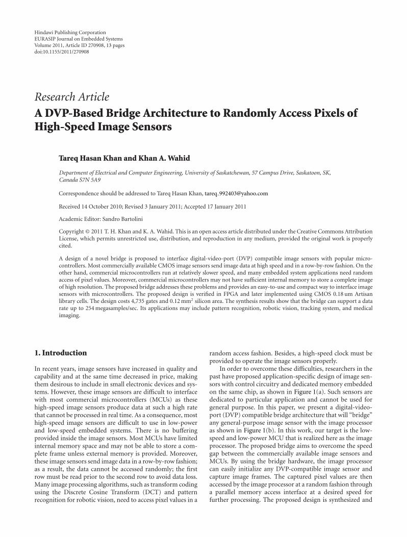
In order to overcome these difficulties, researchers in thepast have proposed application-specific design of image sen-sors with control circuitry and dedicated memory embeddedon the same chip, as shown in Figure 1(a). Such sensors arededicated to particular application and cannot be used forgeneral purpose. In this paper, we present a digital-video-port (DVP) compatible bridge architecture that will “bridge”any general-purpose image sensor with the image processoras shown in Figure 1(b). In this work, our target is the low-speed and low-power MCU that is realized here as the imageprocessor. The proposed bridge aims to overcome the speedgap between the commercially available image sensors andMCUs. By using the bridge hardware, the image processorcan easily initialize any DVP-compatible image sensor andcapture image frames. The captured pixel values are thenaccessed by the image processor at a random fashion througha parallel memory access interface at a desired speed forfurther processing. The proposed design is synthesized and
2 EURASIP Journal on Embedded Systems
Image sensor(dedicated)
Imageprocessor(general)
Controlcircuitry
Memory(fixed)
Imagesensor
(general) Proposed bridgehardware
Controlcircuitry
Memory(variable)
Imageprocessor(general)
Figure 1: Image processor connected with (a) application-specificimage sensor and (b) general-purpose image sensor via theproposed bridge.
tested in commercial FPGA board, where the maximumspeed achieved is 248MHz. The VLSI design using standard0.18 um CMOS Artisan library cells is also presented. Thebridge can be used in various embedded system applicationsincluding pattern recognition, robotic vision, biomedicalimaging, tracking system, where random access of imagepixels is required.
It should be noted that the commercial high-speedimage sensors may be interfaced with more advanced MCUs(such as AT91CAP7E, AT91SAM7S512 from Atmel [1]).However, these microcontrollers contain many additionalfeatures (such as six-layer advanced high-speed bus (AHB),peripheral DMA controller, USB 2.0 full-speed device, andconfigurable FPGA Interface) that may not be required forsimple imaging applications. Besides, programming suchmicrocontrollers and implementing the required protocolsincrease the design cycle time. The purpose of the proposedbridge hardware is to provide a compact, ready-made, andeasy-to-use solution that enables interfacing of commercialgeneral-purpose image sensors with simple microcontrollersthat are low-cost and easy-to-program (such as 8051 [2, 3],AVR [4], and PIC [5]). Thus the bridge hardware helps toshorten the design/development cycle time and facilitatesrapid system level prototyping.
2. Background
In [6–10], presented are some VLSI designs on CMOSimage sensors with random access. In [11, 12], the authorshave presented two different designs of a random accessimage sensor based on a data-address bus structure. Thework in [13] presents a low-power full-custom CMOSdigital pixel sensor array designed for a wireless endoscopycapsule [14]. The proposed architecture reduces the on-chip memory requirement by sharing pixel-level memoryin the sensor array with the digital image processor. Adental digital radiographic (DDR) system using a high-resolution charge-coupled device (CCD) imaging sensor wasdeveloped and its performance for dental clinic imaging wasevaluated in [15]. The work in [16] presents a novel smartCMOS image sensor integrating hot pixel correcting readout
circuit to preserve the quality of the captured images forbiomedical applications. In [17], an image sensor with animage compression feature using the 4× 4 DCT is presented.In [18], a CMOS image sensor has been designed to performthe front-end image decomposition in a Prediction-SPIHTimage compression scheme. In [19], an image sensor unitwith sensor to detect the gravity direction and a built-inimage rotation algorithm is presented. The system rotates thecaptured image in the direction of gravity for better viewingthat can be used in rescue robots. The paper in [20] discussesa range image sensor using a multispot laser projector forrobotic applications. In [21], a pointing device using themotion detection algorithm and its system architecture ispresented. The proposed motion detection pointing deviceuses just binary images of the binary CMOS image sensor(BCIS). In [22], a smart image sensor for real-time andhigh-resolution three-dimensional (3D) measurement to beused for sheet light projection is presented. A facial imagerecognition system based on 3D real-time facial imagingby using correlation image sensor is discussed in [23].The differential geometry theory was employed to find thekey points of face image. A design of an image sensorfocusing on image identification by adjusting the brightnessis presented in [24]. It has GPRS connectivity and canbe used in vehicle surveillance system. In [25], a single-chip image sensor for mobile applications realized in astandard 0.35 um CMOS technology is presented. In [26], asolution to reduce the computational complexity of imageprocessing by performing some low-level computations onthe sensor focal plane is presented. An autonomous imagesensor for real-time target detection and tracking is presentedin [27]. In [28], the authors describe and analyse a novelCMOS pixel for high-speed, low-light imaging applications.An 8.3-M-pixel digital-output CMOS active pixel imagesensor (APS) for ultra-definition TV (UDTV) application isdiscussed in [29]. In [30], a hardware accelerator for imagereconstruction in digital holographic imaging is presentedthat focuses to maximize the computational efficiency andminimize the memory transfer overhead to the externalSDRAM.
There are some commercial image sensors such asMT9V011 from Aptina [31] and OVM7690 from OmniVi-sion [32] that support partial access of image segmentsknown as “windowing”. By configuring the control resisters,the top-left and bottom-right corners of the desired area canbe specified. The image sensor then captures and sends animage of the specified rectangle. However, it is not possibleto access (and capture) other segments of the same framewith this feature which is required in several image codingapplications such as transform coding. There are two moredisadvantages of such approach: firstly, the internal controlregisters need to be reconfigured every time an image capturerequest is sent, which is an extra overhead; secondly, becauseof the time taken for this reconfiguration, the sensor willcapture a frame that is different in the time instant. Besides,the “windowing” is limited to rectangles only; the image datacannot be accessed in any other shapes.
In summary, the works mentioned above discuss differ-ent designs of image sensors targeted to specific application;
EURASIP Journal on Embedded Systems 3
however, they are not available for general-purpose use. Inthis paper, we present a novel concept—the design of abridge architecture that connects the commercial MCUs toany commercial DVP-based general-purpose image sensors.The bridge needs to be configured once with a set ofaddresses (provided by the manufacture as found in thedatasheet) in order to communicate with the image sensor,which makes the design universal and for general-purposeuse.
3. Design Objectives
Considering the application types (i.e., robotics vision,imaging, video, etc.) and availability of commercial micro-controllers (MCUs), in this work, we have set the followingdesign objectives to facilitate the interfacing of high-speedimage sensors with low-performance MCU.
(i) The bridge hardware should operate at very highspeed (over 200MHz) so that the image pixels canbe accessed in real time through high-speed imagesensors. As a result, the MCUs (or image processor)using the bridge need not be high performance andhigh speed.
(ii) The bridge should contain sufficient memory spaceto store image frames of different resolutions, suchas CIF, QVGA, VGA, full HD, and UHDV. Thus,an MCU with limited on-chip memory may be ableto access image pixels from the buffer memory ofthe bridge at the desired speed. Moreover, becauseof the memory buffer, any image segments of thesame frame can be accessed without having toreconfigure the image sensor, which is required inmany video coding applications. An example of suchapplication is the Discrete Cosine Transform-basedimage coding, where several 8 × 8 blocks of imagesegments of the same frame are required.
(iii) The bridge should provide an efficient way to accessthe image pixels randomly. A more convenient way isto access the 2D pixel arrays using parallel interfacingwith row and column positions. This will be asignificant improvement over the designs with typicaldata-address structure [11, 12].
(iv) The usage of the bridge should be robust. As aresult, it should provide efficient and easy ways toaccess image pixels in virtually any shapes, such asrectangles, circles, oval, and points. This facilitatesfully random access in any random shapes.
(v) Commercial image sensors from different vendorshave unique device parameters along with internalcontrol registers for proper configuration (such as,to configure frame size, colour, and sleep mode).The bridge should be able to communicate withmost available image sensors. As a result, the designshould be universal so that it can be configured atthe beginning with the proper set of parameters fora particular image sensor.
CMOS imagesensor
VD
HD
DCLK
DOUT(7:0)
STROBE
GPIO
EXTCLK
RESET
PWDN
SCL
SDA
TEST
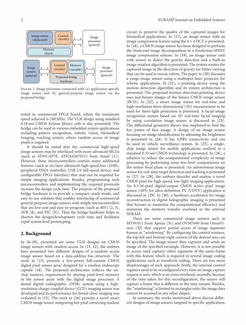
Figure 2: DVP interface pins of an image sensor.
(vi) Commercial image sensors use I2C protocol andDVP interfacing. Hence, the desired bridge hardwaremust have I2C protocol already configured as well assupport DVP interfacing.
(vii) Most commercial image sensors require high-speedexternal clock for its operation. It is desirable thatthe bridge supplies that clock so that the clock canbe efficiently controlled during operation (i.e., fullclock rate during regular operation, reduced rateduring sleep or inactivity, etc.). At the same time,the bridge should be able to detect any inactivity andautomatically enable the sleep mode of the imagesensor—this will result in power savings.
4. The DVP Interface
Most leading commercial CMOS image sensors, bothstandard-definition (SD) and high-definition (HD), sendimage data using a common standard interface, known asthe DVP interface. The common I/O pins of a typical CMOSimage sensor are shown in Figure 2.
The VD (or VSYNC) and HD (or HSYNC) pins indicatethe end of frame and end of row, respectively. Pixel databytes are available for sampling at the DOUT(0 : 7) bus atthe positive edge of the DCLK signal. The EXTCLK is theclock input for the image sensor. The frequency of DCLK ishalf or quarter of the frequency of EXTCLK depending onthe configuration of the image sensor. The initialization andconfiguration of the image sensor is done by the 2-wire (SCLand SDA) I2C protocol. In the context of image sensor, it isoften called as Serial Camera Control Bus (SCCB) interface[32]. The frame size, colour, sleep mode, and wake up modecan be controlled by sending I2C commands to the imagesensor. The RESET is an active low reset signal for the imagesensor. Some image sensors have a pin (PWDN) to controlthe active-sleep mode. Some HD image sensors may containadditional control pins (as shown as dotted line in Figure 2),which are used in special modes; however, these extra pinsmay be tied to VDD or GND or left unconnected in normaloperation.
4.1. Standard-Definition (SD) CMOS Image Sensors. TheDVP interface is widely used in most commercially available
4 EURASIP Journal on Embedded Systems
Random access memory
Memoryaddressingand control
Read addressgenerator
Image data module
I2C interfaceSensorcontrol
I2C CLK
Clockgenerator
Configure module
iBRIDGE
VD
HDDOUT (9:0)
RESET
SCL
SDA
EXTCLK
DCLK
PWDN
Imag
ese
nso
rin
terf
ace
Data(9:0)
FrameReceived
CfgWr
Init
ReqFrame
RST
Crystal
Imag
epr
oces
sor
inte
rfac
e
Col(9:0)/CfgAdr(3:0)
Row(8:0)/CfgData(7:0)
ByteIndex(1:0)
Figure 3: Block diagram of the iBRIDGE.
SD CMOS image sensors, such as TCM8230MD fromToshiba [33], OVM7690 from OmniVision [32], MT9V011from Aptina [31], LM9618 from National [34], KAC-9630from Kodak [35], and PO6030K from Pixelplus [36].
4.2. High-Definition (HD) CMOS Image Sensors. Most nativeHD (720p and 1080p) image sensors such as OV10131 fromOmniVision [32] and MT9P401 from Aptina [31] use theDVP interface. Some higher-resolution HD image sensorssuch as OV9810 [32] use an additional interface, calledthe mobile industry processor interface (MIPI) along withthe typical DVP interface. The data output bus DOUT isgenerally wider than 8 bits in these HD image sensors.
5. The iBRIDGE Architecture
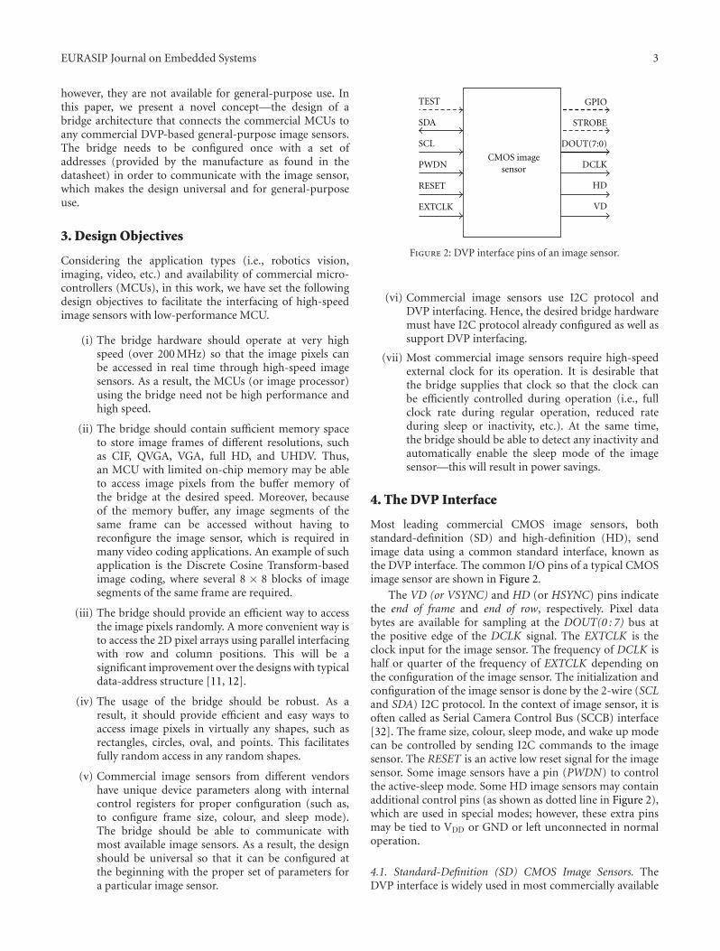
The proposed bridge (referred as iBRIDGE from now) isplaced in between the image sensor and the image processoror the microcontroller. Figure 3 shows the interfacing of theiBRIDGE and its internal blocks. The pins on the left handside are to be connected with an image sensor while thoseon the right hand side are to be connected to the imageprocessor (or the MCU). There are two types of signalscoming from the Image Processor Interface: configurationsignals (CfgWr, Init, ReqFrame, and RST) and frame accesssignals (Data, Col, Row, etc.). The configuration signals areasynchronous in nature whereas the frame access signalsdepend on the speed of the image processor requesting the“access”; hence these incoming signals do not need to besynchronized with iBRIDGE’s internal clock.
5.1. Configuring the iBRIDGE. The operation starts by firstconfiguring the iBRIDGE’s internal registers with a set of
Table 1: Configuration register mapping.
CfgAdr(3 : 0) CfgData(7 : 0) CfgAdr(3 : 0) CfgData(7 : 0)
0000 Device ID 1000 Cmd2 Reg. Adr.
0001 Total Cmd. 1001 Cmd2 Reg. Data
0010 Sleep Reg. Adr. 1010 Cmd3 Reg. Adr.
0011 Sleep Reg. Data 1011 Cmd3 Reg. Data
0100 Wake Reg. Adr. 1100 Cmd4 Reg. Adr.
0101 Wake Reg. Data 1101 Cmd4 Reg. Data
0110 Cmd1 Reg. Adr. 1110 ImageWidth/4
0111 Cmd1 Reg. Data 1111 Bytes-per-pixel
predefined addresses so that it can properly communicatewith the image sensor. Image sensors of different manufac-tures have different device ID (or slave address) which isused for such communication using the I2C protocol [37].The image sensors also have internal control registers usedto configure the functionality, such as frame size, colour,and sleep mode, and so forth. These registers are controlledby I2C protocol. The register mapping is also differentfor different manufacturers; so, the iBRIDGE needs to beconfigured as well with the proper configuration mappingof the image sensor (found on the datasheet). Table 1 showsthe configuration registers implemented inside the iBRIDGEthat are required in normal operation. The table may beextended to accommodate additional special features. Thecontent of these registers can be modified by twomultiplexedinput ports: CfgAdr(3 : 0) and CfgData(7 : 0). In order towrite to a register of iBRIDGE, the register address is placedon CfgAdr(3 : 0) bus, the data on CfgData(7 : 0) bus, and
EURASIP Journal on Embedded Systems 5
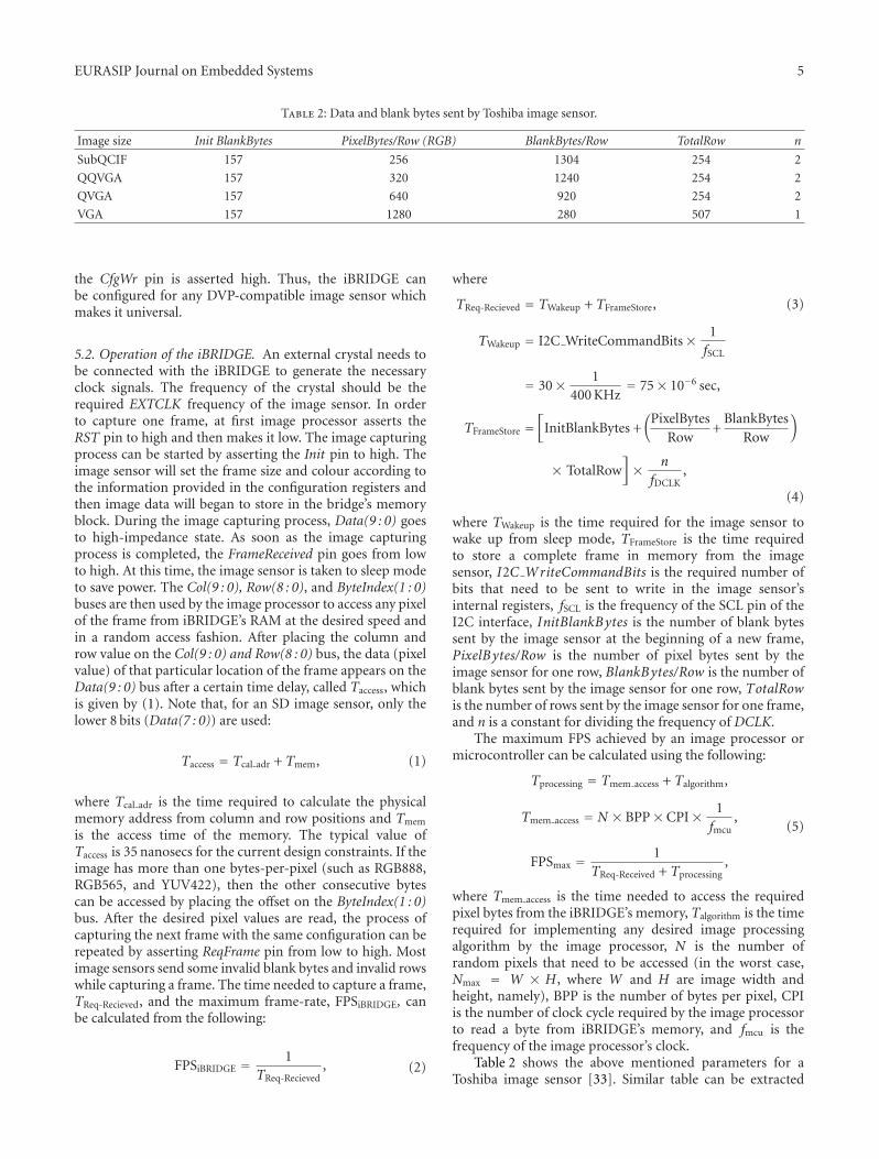
Table 2: Data and blank bytes sent by Toshiba image sensor.
Image size Init BlankBytes PixelBytes/Row (RGB) BlankBytes/Row TotalRow n
SubQCIF 157 256 1304 254 2
QQVGA 157 320 1240 254 2
QVGA 157 640 920 254 2
VGA 157 1280 280 507 1
the CfgWr pin is asserted high. Thus, the iBRIDGE canbe configured for any DVP-compatible image sensor whichmakes it universal.
5.2. Operation of the iBRIDGE. An external crystal needs tobe connected with the iBRIDGE to generate the necessaryclock signals. The frequency of the crystal should be therequired EXTCLK frequency of the image sensor. In orderto capture one frame, at first image processor asserts theRST pin to high and then makes it low. The image capturingprocess can be started by asserting the Init pin to high. Theimage sensor will set the frame size and colour according tothe information provided in the configuration registers andthen image data will began to store in the bridge’s memoryblock. During the image capturing process, Data(9 : 0) goesto high-impedance state. As soon as the image capturingprocess is completed, the FrameReceived pin goes from lowto high. At this time, the image sensor is taken to sleep modeto save power. The Col(9 : 0), Row(8 : 0), and ByteIndex(1 : 0)buses are then used by the image processor to access any pixelof the frame from iBRIDGE’s RAM at the desired speed andin a random access fashion. After placing the column androw value on the Col(9 : 0) and Row(8 : 0) bus, the data (pixelvalue) of that particular location of the frame appears on theData(9 : 0) bus after a certain time delay, called Taccess, whichis given by (1). Note that, for an SD image sensor, only thelower 8 bits (Data(7 : 0)) are used:
Taccess = Tcal adr + Tmem, (1)
where Tcal adr is the time required to calculate the physicalmemory address from column and row positions and Tmem
is the access time of the memory. The typical value ofTaccess is 35 nanosecs for the current design constraints. If theimage has more than one bytes-per-pixel (such as RGB888,RGB565, and YUV422), then the other consecutive bytescan be accessed by placing the offset on the ByteIndex(1 : 0)bus. After the desired pixel values are read, the process ofcapturing the next frame with the same configuration can berepeated by asserting ReqFrame pin from low to high. Mostimage sensors send some invalid blank bytes and invalid rowswhile capturing a frame. The time needed to capture a frame,TReq-Recieved, and the maximum frame-rate, FPSiBRIDGE, canbe calculated from the following:
FPSiBRIDGE = 1TReq-Recieved
, (2)
where
TReq-Recieved = TWakeup + TFrameStore, (3)
TWakeup = I2C WriteCommandBits× 1fSCL
= 30× 1400KHz
= 75× 10−6 sec,
TFrameStore =[InitBlankBytes +
(PixelBytes
Row+BlankBytes
Row
)
× TotalRow]× n
fDCLK,
(4)
where TWakeup is the time required for the image sensor towake up from sleep mode, TFrameStore is the time requiredto store a complete frame in memory from the imagesensor, I2C WriteCommandBits is the required number ofbits that need to be sent to write in the image sensor’sinternal registers, fSCL is the frequency of the SCL pin of theI2C interface, InitBlankBytes is the number of blank bytessent by the image sensor at the beginning of a new frame,PixelBytes/Row is the number of pixel bytes sent by theimage sensor for one row, BlankBytes/Row is the number ofblank bytes sent by the image sensor for one row, TotalRowis the number of rows sent by the image sensor for one frame,and n is a constant for dividing the frequency of DCLK.
The maximum FPS achieved by an image processor ormicrocontroller can be calculated using the following:
Tprocessing = Tmem access + Talgorithm,
Tmem access = N × BPP× CPI× 1fmcu
,
FPSmax = 1TReq-Received + Tprocessing
,
(5)
where Tmem access is the time needed to access the requiredpixel bytes from the iBRIDGE’s memory, Talgorithm is the timerequired for implementing any desired image processingalgorithm by the image processor, N is the number ofrandom pixels that need to be accessed (in the worst case,Nmax = W × H , where W and H are image width andheight, namely), BPP is the number of bytes per pixel, CPIis the number of clock cycle required by the image processorto read a byte from iBRIDGE’s memory, and fmcu is thefrequency of the image processor’s clock.
Table 2 shows the above mentioned parameters for aToshiba image sensor [33]. Similar table can be extracted
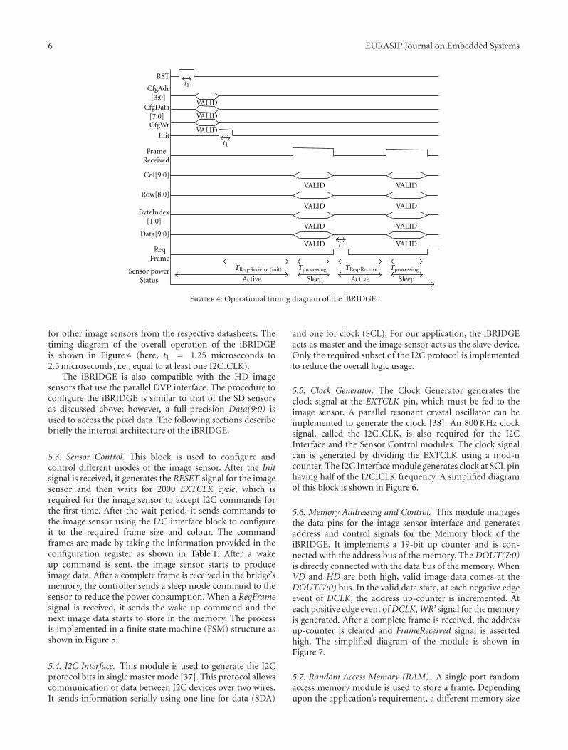
6 EURASIP Journal on Embedded Systems
VALID
VALID
VALID
VALID
VALID
VALID
VALID
VALID
VALID
VALID
VALID
RST
CfgAdr[3:0]
CfgData[7:0]CfgWr
Init
FrameReceived
Col[9:0]
Row[8:0]
ByteIndex[1:0]
Data[9:0]
ReqFrame
TReq-Recieive (init) Tprocessing TReq-Receive Tprocessing
t1
t1
t1
Sensor powerStatus Active Sleep Active Sleep
Figure 4: Operational timing diagram of the iBRIDGE.
for other image sensors from the respective datasheets. Thetiming diagram of the overall operation of the iBRIDGEis shown in Figure 4 (here, t1 = 1.25 microseconds to2.5microseconds, i.e., equal to at least one I2C CLK).
The iBRIDGE is also compatible with the HD imagesensors that use the parallel DVP interface. The procedure toconfigure the iBRIDGE is similar to that of the SD sensorsas discussed above; however, a full-precision Data(9:0) isused to access the pixel data. The following sections describebriefly the internal architecture of the iBRIDGE.
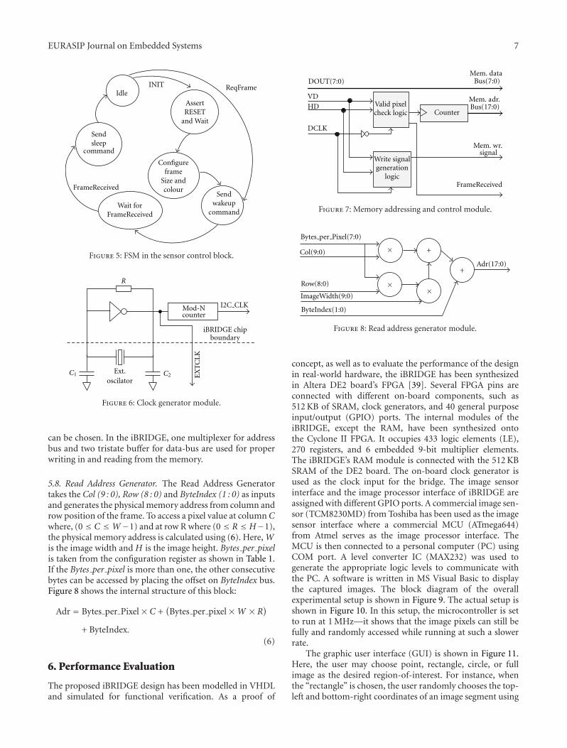
5.3. Sensor Control. This block is used to configure andcontrol different modes of the image sensor. After the Initsignal is received, it generates the RESET signal for the imagesensor and then waits for 2000 EXTCLK cycle, which isrequired for the image sensor to accept I2C commands forthe first time. After the wait period, it sends commands tothe image sensor using the I2C interface block to configureit to the required frame size and colour. The commandframes are made by taking the information provided in theconfiguration register as shown in Table 1. After a wakeup command is sent, the image sensor starts to produceimage data. After a complete frame is received in the bridge’smemory, the controller sends a sleep mode command to thesensor to reduce the power consumption. When a ReqFramesignal is received, it sends the wake up command and thenext image data starts to store in the memory. The processis implemented in a finite state machine (FSM) structure asshown in Figure 5.
5.4. I2C Interface. This module is used to generate the I2Cprotocol bits in singlemastermode [37]. This protocol allowscommunication of data between I2C devices over two wires.It sends information serially using one line for data (SDA)
and one for clock (SCL). For our application, the iBRIDGEacts as master and the image sensor acts as the slave device.Only the required subset of the I2C protocol is implementedto reduce the overall logic usage.
5.5. Clock Generator. The Clock Generator generates theclock signal at the EXTCLK pin, which must be fed to theimage sensor. A parallel resonant crystal oscillator can beimplemented to generate the clock [38]. An 800KHz clocksignal, called the I2C CLK, is also required for the I2CInterface and the Sensor Control modules. The clock signalcan is generated by dividing the EXTCLK using a mod-ncounter. The I2C Interfacemodule generates clock at SCL pinhaving half of the I2C CLK frequency. A simplified diagramof this block is shown in Figure 6.
5.6. Memory Addressing and Control. This module managesthe data pins for the image sensor interface and generatesaddress and control signals for the Memory block of theiBRIDGE. It implements a 19-bit up counter and is con-nected with the address bus of the memory. The DOUT(7:0)is directly connected with the data bus of the memory. WhenVD and HD are both high, valid image data comes at theDOUT(7:0) bus. In the valid data state, at each negative edgeevent of DCLK, the address up-counter is incremented. Ateach positive edge event ofDCLK,WR’ signal for thememoryis generated. After a complete frame is received, the addressup-counter is cleared and FrameReceived signal is assertedhigh. The simplified diagram of the module is shown inFigure 7.
5.7. Random Access Memory (RAM). A single port randomaccess memory module is used to store a frame. Dependingupon the application’s requirement, a different memory size
EURASIP Journal on Embedded Systems 7
IdleAssertRESET
and Wait
Configureframe
Size andcolour
Sendwakeup
commandWait for
FrameReceived
command
Sendsleep
INIT
FrameReceived
ReqFrame
Figure 5: FSM in the sensor control block.
I2C CLKMod-Ncounter
EX
TC
LK
R
C1 C2Ext.
oscilator
iBRIDGE chipboundary
Figure 6: Clock generator module.
can be chosen. In the iBRIDGE, one multiplexer for addressbus and two tristate buffer for data-bus are used for properwriting in and reading from the memory.
5.8. Read Address Generator. The Read Address Generatortakes the Col (9 : 0), Row (8 : 0) and ByteIndex (1 : 0) as inputsand generates the physical memory address from column androw position of the frame. To access a pixel value at columnCwhere, (0 ≤ C ≤W−1) and at row R where (0 ≤ R ≤ H−1),the physical memory address is calculated using (6). Here,Wis the image width and H is the image height. Bytes per pixelis taken from the configuration register as shown in Table 1.If the Bytes per pixel is more than one, the other consecutivebytes can be accessed by placing the offset on ByteIndex bus.Figure 8 shows the internal structure of this block:
Adr = Bytes per Pixel× C +(Bytes per pixel×W × R
)
+ ByteIndex.(6)
6. Performance Evaluation
The proposed iBRIDGE design has been modelled in VHDLand simulated for functional verification. As a proof of
Counter
DCLK
Valid pixelcheck logic
VD
Write signalgeneration
logic
HD
Mem. data
Mem. adr.
Mem. wr.signal
FrameReceived
Bus(17:0)
DOUT(7:0) Bus(7:0)
Figure 7: Memory addressing and control module.
×
××
+
+Adr(17:0)
Bytes per Pixel(7:0)
Col(9:0)
Row(8:0)
ImageWidth(9:0)
ByteIndex(1:0)
Figure 8: Read address generator module.
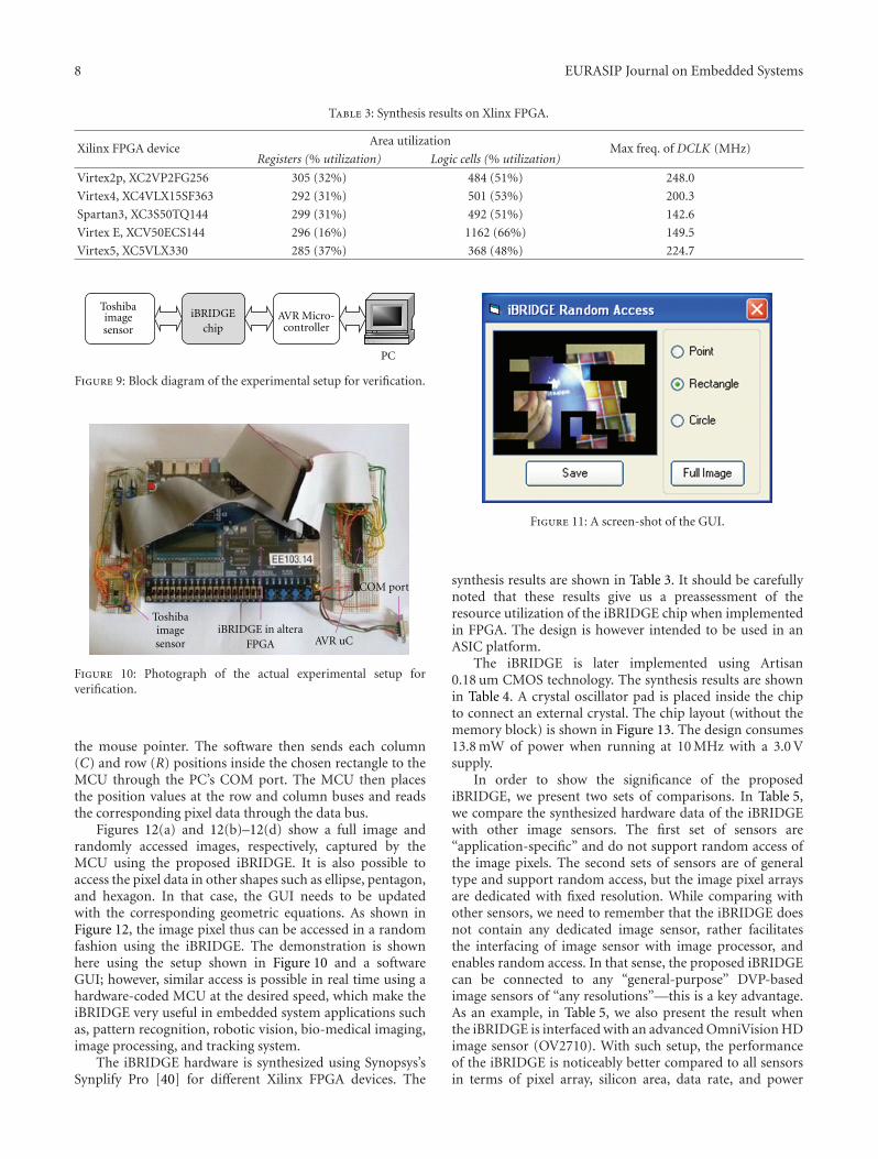
concept, as well as to evaluate the performance of the designin real-world hardware, the iBRIDGE has been synthesizedin Altera DE2 board’s FPGA [39]. Several FPGA pins areconnected with different on-board components, such as512KB of SRAM, clock generators, and 40 general purposeinput/output (GPIO) ports. The internal modules of theiBRIDGE, except the RAM, have been synthesized ontothe Cyclone II FPGA. It occupies 433 logic elements (LE),270 registers, and 6 embedded 9-bit multiplier elements.The iBRIDGE’s RAM module is connected with the 512KBSRAM of the DE2 board. The on-board clock generator isused as the clock input for the bridge. The image sensorinterface and the image processor interface of iBRIDGE areassigned with different GPIO ports. A commercial image sen-sor (TCM8230MD) from Toshiba has been used as the imagesensor interface where a commercial MCU (ATmega644)from Atmel serves as the image processor interface. TheMCU is then connected to a personal computer (PC) usingCOM port. A level converter IC (MAX232) was used togenerate the appropriate logic levels to communicate withthe PC. A software is written in MS Visual Basic to displaythe captured images. The block diagram of the overallexperimental setup is shown in Figure 9. The actual setup isshown in Figure 10. In this setup, the microcontroller is setto run at 1MHz—it shows that the image pixels can still befully and randomly accessed while running at such a slowerrate.
The graphic user interface (GUI) is shown in Figure 11.Here, the user may choose point, rectangle, circle, or fullimage as the desired region-of-interest. For instance, whenthe “rectangle” is chosen, the user randomly chooses the top-left and bottom-right coordinates of an image segment using
8 EURASIP Journal on Embedded Systems
Table 3: Synthesis results on Xlinx FPGA.
Xilinx FPGA deviceArea utilization
Max freq. of DCLK (MHz)Registers (% utilization) Logic cells (% utilization)
Virtex2p, XC2VP2FG256 305 (32%) 484 (51%) 248.0
Virtex4, XC4VLX15SF363 292 (31%) 501 (53%) 200.3
Spartan3, XC3S50TQ144 299 (31%) 492 (51%) 142.6
Virtex E, XCV50ECS144 296 (16%) 1162 (66%) 149.5
Virtex5, XC5VLX330 285 (37%) 368 (48%) 224.7
PC
Toshibaimagesensor
iBRIDGEchip
AVR Micro-controller
Figure 9: Block diagram of the experimental setup for verification.
Toshibaimagesensor
iBRIDGE in alteraFPGA AVR uC
COM port
Figure 10: Photograph of the actual experimental setup forverification.
the mouse pointer. The software then sends each column(C) and row (R) positions inside the chosen rectangle to theMCU through the PC’s COM port. The MCU then placesthe position values at the row and column buses and readsthe corresponding pixel data through the data bus.
Figures 12(a) and 12(b)–12(d) show a full image andrandomly accessed images, respectively, captured by theMCU using the proposed iBRIDGE. It is also possible toaccess the pixel data in other shapes such as ellipse, pentagon,and hexagon. In that case, the GUI needs to be updatedwith the corresponding geometric equations. As shown inFigure 12, the image pixel thus can be accessed in a randomfashion using the iBRIDGE. The demonstration is shownhere using the setup shown in Figure 10 and a softwareGUI; however, similar access is possible in real time using ahardware-coded MCU at the desired speed, which make theiBRIDGE very useful in embedded system applications suchas, pattern recognition, robotic vision, bio-medical imaging,image processing, and tracking system.
The iBRIDGE hardware is synthesized using Synopsys’sSynplify Pro [40] for different Xilinx FPGA devices. The
Figure 11: A screen-shot of the GUI.
synthesis results are shown in Table 3. It should be carefullynoted that these results give us a preassessment of theresource utilization of the iBRIDGE chip when implementedin FPGA. The design is however intended to be used in anASIC platform.
The iBRIDGE is later implemented using Artisan0.18 um CMOS technology. The synthesis results are shownin Table 4. A crystal oscillator pad is placed inside the chipto connect an external crystal. The chip layout (without thememory block) is shown in Figure 13. The design consumes13.8mW of power when running at 10MHz with a 3.0 Vsupply.
In order to show the significance of the proposediBRIDGE, we present two sets of comparisons. In Table 5,we compare the synthesized hardware data of the iBRIDGEwith other image sensors. The first set of sensors are“application-specific” and do not support random access ofthe image pixels. The second sets of sensors are of generaltype and support random access, but the image pixel arraysare dedicated with fixed resolution. While comparing withother sensors, we need to remember that the iBRIDGE doesnot contain any dedicated image sensor, rather facilitatesthe interfacing of image sensor with image processor, andenables random access. In that sense, the proposed iBRIDGEcan be connected to any “general-purpose” DVP-basedimage sensors of “any resolutions”—this is a key advantage.As an example, in Table 5, we also present the result whenthe iBRIDGE is interfaced with an advancedOmniVisionHDimage sensor (OV2710). With such setup, the performanceof the iBRIDGE is noticeably better compared to all sensorsin terms of pixel array, silicon area, data rate, and power

EURASIP Journal on Embedded Systems 9
(a) (b)
(c) (d)
Figure 12: Captured image: (a) full image; (b)–(d) randomly accessed pixel image using the iBRIDGE.
Rea
dad
dres
sge
ner
ator
Sensor control
Memory addressingand control
I2C
Clockgenerator
MUX &buffers
Figure 13: Chip layout of the iBRIDGE core.
consumption. Note that, in Table 5, the die area (i.e., corearea plus the I/O pads) is used for the iBRIDGE.
In Table 6, we present the performance of the iBRIDGEwhen interfaced with both SD (TCM8230MD) and HD(OV2710) image sensors. It can be seen that, with avery little increase in hardware (i.e., 1.96mm2) and powerconsumption (i.e., 13.8mW), any DVP-compatible com-mercial image sensor can be converted to a high-speed
Table 4: Synthesis results in ASIC.
Inputs/Outputs 36/17
Technology 0.18 um CMOS
Die dimension (W ×H) 1.4mm× 1.4mm
Core dimension (W ×H) 0.4mm× 0.3mm
Number of cells 1,446
Number of gates 4,735
Max DCLK frequency 254MHz
Core power consumption 13.8mW @ 3.0V
randomly accessible image sensor. Given the data rate, thatis 254megasamples/sec and the equations in Section 4.1, theiBRIDGE supports 333 fps for the VGA (640 × 480) and56 fps for the full HD (1920 × 1080) resolution. It is worthnoticing from Tables 5 and 6 that this data rate supported bythe iBRIDGE is much higher than other image sensors forsame frame resolution.
To show the advantages of the proposed iBRIDGE, inTable 7 we compare the performance of a low-performanceMCU interfaced with iBRIDGE with high-performanceMCUs. The comparison is based on two scenarios: onewhere a high-speed image sensor is connected with a high-performance MCU, and another where the same sensor is
10 EURASIP Journal on Embedded Systems
High-speedimagesensor
High performance
MCU
(e.g., AT91CAP7E)
(a)
High-speedimagesensor
iBridgeH/W
Low performanceMCU
(e.g., ATmega644)
(b)
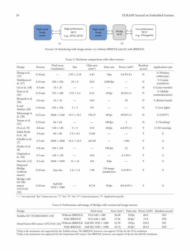
Figure 14: Interfacing with image sensor: (a) without iBRIDGE and (b) with iBRIDGE.
Table 5: Hardware comparisons with other sensors.
Design ProcessPixel array(resolution)
SizeChip area(mm2)
Data rate Power (mW)Randomaccess?
Application type
Zhang et al.[13]
0.18 um — 2.95× 2.18 6.43 2 fps 3.6 @1.8 v NS (Wirelessendoscopy)
Nishikawa etal. [17]
0.25 um 256× 256 10× 5 50.0 3,000 fps — NS (Cosinetransform)
Lin et al. [18] 0.5 um 33× 25 — — — — N S (Lossy wavelet)
Yoon et al.[25]
0.35 um 352× 288 3.55× 2.4 8.52 30 fps 20 @3.3 v NS (Mobile
communication)
Elouardi et al.[26]
0.6 um 16× 16 — 10.0 — 30 N S (Retina based)
Ji andAbshire [28]
0.18 um 256× 256 3× 3 9.0 — — N S (Low light)
Takayanagi etal. [29]
0.25 um 3840× 2160 19.7× 19.1 376.27 60 fps [email protected] v N S (UDTV)
Teman et al.[27]
0.18 um 64× 64 — — 100 fps 2 N S (Tracking)
Oi et al. [9] 0.8 um 128× 128 5× 5 25.0 60 fps 6.8 @3.3 v Y S (3D viewing)
Yadid-Pechtet al. [6]
3.0 um 80× 80 7.9× 9.2 72.68 — — Y G
Scheffer et al.[7]
0.5 um 2048× 2048 16.3× 16.5 265.69 — <100 Y G
Decker et al.[8]
0.8 um 256× 256 — — 390 fps 52 Y G
Chapinal etal. [10]
0.7 um 128× 128 — 16.0 — 6.5 @5 v Y G
Dierickx [12] 0.5 um 2048× 2048 16× 16 256 8 fps — Y G
ProposediBridge(withoutsensor)
0.18 um Any size 1.4× 1.4 1.96254mega-samples/sec
13.8 @3 v Y G
iBridge withOV HDsensor(OV2710)[32]
0.18 umFull HD
1920× 1080— 45.74 30 fps 363.8 @3 v Y G
“—”: not reported; “fps”: frames per sec; “Y”: Yes; “N”: No; “G”: General purpose; “S”: Application specific.
Table 6: Performance advantage of iBridge with commercial image sensors.
Design Pixel array Area (mm2) Data rate Power (mW) Random access?
Toshiba SD (TCM8230MD) [33] Without iBRIDGE VGA 640× 480 36.00 30 fps 60.0 NO
With iBRIDGE VGA 640× 480 37.96 30 fps1 73.8 YES
OmniVision HD sensor (OV2710) [32]Without iBRIDGE Full HD 1920× 1080 43.78 30 fps 350.0 NO
With iBRIDGE Full HD 1920× 1080 45.74 30 fps2 363.8 YES130 fps is the maximum rate supported by the Toshiba sensor. The iBRIDGE, however, can support 333 fps for the VGA resolution.230 fps is the maximum rate supported by the Omnivision HD sensor. The iBRIDGE, however, can support 56 fps for the full HD resolution.
EURASIP Journal on Embedded Systems 11
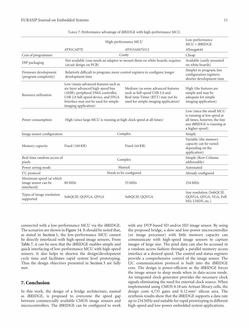
Table 7: Performance advantage of iBRIDGE with high-performance MCU.
High-performance MCU Low-performanceMCU+ iBRIDGE
AT91CAP7E AT91SAM7S512 ATmega644
Cost of programmer Costly Cheap
DIP packagingNot available (one needs an adaptor to mount them on white boards; requirescircuit design on PCB)
Available (easily mountedon white boards)
Firmware development(program complexity)
Relatively difficult to program; more control registers to configure; longerdevelopment time
Simpler to program; lessconfiguration registers;shorter development time
Resource utilization
Low (many advanced features such assix-layer advanced high-speed bus(AHB), peripheral DMA controller,USB 2.0 full-speed device, and FPGAInterface may not be used for simpleimaging application)
Medium (as some advanced featuressuch as full-speed USB 2.0 andReal-time Timer (RTT) may not beused for simple imaging application)
High (the features aresimple and may beadequate for simpleimaging application)
Power consumption High (since large MCU is running at high clock speed at all times)
Low (since the small MCUis running at low speed atall times, however, the tinysize iBRIDGE is running ata higher speed)
Image sensor configuration Complex Simple
Memory capacity Fixed (160KB) Fixed (64KB)
Variable (the memorycapacity can be varieddepending on theapplication)
Real-time random access ofpixels
Complex Simple (Row-Columnaddressable)
Power saving mode Manual Automated
I2C protocol Needs to be configured Already configured
Maximum speed (at whichimage sensor can beinterfaced)
80MHz 55MHz 254MHz
Types of image resolutionsupported
SubQCIF, QQVGA, QVGA SubQCIF, QQVGAAny resolution (SubQCIF,QQVGA, QVGA, VGA, FullHD, UHDV, etc.)
connected with a low-performance MCU via the iBRIDGE.The scenarios are shown in Figure 14. It should be noted that,as stated in Section 1, the low-performance MCU cannotbe directly interfaced with high-speed image sensors. FromTable 7, it can be seen that the iBRIDGE enables simple andquick interfacing of low-performance MCU with high-speedsensors. It also helps to shorten the design/developmentcycle time and facilitates rapid system level prototyping.Thus the design objectives presented in Section 3 are fullymet.
7. Conclusion
In this work, the design of a bridge architecture, namedas iBRIDGE, is proposed to overcome the speed gapbetween commercially available CMOS image sensors andmicrocontrollers. The iBRIDGE can be configured to work
with any DVP-based SD and/or HD image sensor. By usingthe proposed bridge, a slow and low-power microcontroller(or image processor) with little memory capacity cancommunicate with high-speed image sensors to captureimages of large size. The pixel data can also be accessed ina random access fashion through a parallel memory accessinterface at a desired speed. The control and status registersprovide a comprehensive control of the image sensor. TheI2C communication protocol is built into the iBRIDGEcore. The design is power-efficient as the iBRIDGE forcesthe image sensor to sleep mode when in data-access mode.An integrated clock generator provides the necessary clocksignals eliminating the need for external clock source. Whenimplemented using CMOS 0.18 um Artisan library cells, thedesign costs 4,735 gates and 0.12mm2 silicon area. Thesynthesis results show that the iBRIDGE supports a data rateup to 254MHz and suitable for rapid prototyping in differenthigh-speed and low-power embedded system applications.
12 EURASIP Journal on Embedded Systems
Acknowledgments
The authors would like to acknowledge the Natural Scienceand Engineering Research Council of Canada (NSERC) forits support to this research work. The authors are alsoindebted to the Canadian Microelectronics Corporation(CMC) for providing the hardware and software infrastruc-ture used in the development of this design.
References
[1] J. Uthus and O. Strom, “MCU architectures for compute-intensive embedded applications,” Atmel White Paper, 2005.
[2] L. Fanucci, S. Saponara, and A. Morello, “Power optimizationof an 8051-compliant IP microcontroller,” IEICE Transactionson Electronics, vol. E88-C, no. 4, pp. 597–600, 2005.
[3] S. Saponara, L. Fanucci, and P. Terreni, “Architectural-levelpower optimization of microcontroller cores in embeddedsystems,” IEEE Transactions on Industrial Electronics, vol. 54,no. 1, pp. 680–683, 2007.
[4] A. Holberg and A. Saetre, “Innovative techniques forextremely low power consumption with 8-bit microcon-trollers,” Atmel White Paper, 2006.
[5] T. Wilmshurt, Designing Embedded Systems with PIC Micro-controllers: Principles and Applications, Newnes, 2007.
[6] O. Yadid-Pecht, R. Ginosar, and Y. Shacham-Diamand, “A ran-dom access photodiode array for intelligent image capture,”IEEE Transactions on Electron Devices, vol. 38, no. 8, pp. 1772–1780, 1991.
[7] D. Scheffer, B. Dierickx, and G. Meynants, “Random address-able 2048 x 2048 active pixel image sensor,” IEEE Transactionson Electron Devices, vol. 44, no. 10, pp. 1716–1720, 1997.
[8] S. Decker, R. D. McGrath, K. Brehmer, and C. G. Sodini,“A 256 x 256 CMOS imaging array with wide dynamic rangepixels and column-parallel digital output,” IEEE Journal ofSolid-State Circuits, vol. 33, no. 12, pp. 2081–2090, 1998.
[9] R. Oi, T. Hamamoto, and K. Aizawa, “Pixel based randomaccess image sensor array for real-time IBR,” in Proceedings ofthe 1st IEEE International Conference on Sensors (Sensors ’02),vol. 1, pp. 134–139, June 2002.
[10] G. Chapinal, S. A. Bota, M. Moreno, J. Palacin, and A. Herms,“A 128 x 128 CMOS image sensor with analog memory forsynchronous image capture,” IEEE Sensors Journal, vol. 2, no.2, pp. 120–127, 2002.
[11] R. L. Baer and V. K. Srikantam, “Imaging parallel interfaceRAM,” U. S. Patent no. 20070024713, July, 2005.
[12] B. Dierickx, D. Scheffer, G. Meynants, W. Ogiers, and J.Vlummens, “Random addressable active pixel image sensors,”in Advanced Focal Plane Arrays and Electronic Cameras, vol.2950 of Proceedings of SPIE, pp. 2–7, Berlin, Germany, October1996.
[13] M. Zhang, A. Bermak, X. Li, and Z. Wang, “A low powerCMOS image sensor design for wireless endoscopy capsule,” inProceedings of IEEE-BIOCAS Biomedical Circuits and SystemsConference (BIOCAS ’08), pp. 397–400, November 2008.
[14] D. O. Faigel and D. Cave,Capsule Endoscopy, Saunders Elsivier,2008.
[15] J. H. Kim, S. G. So, and K. S. Joo, “Development andperformances of a dental digital radiographic system using ahigh resolution CCD image sensor,” in Proceedings of IEEENuclear Science Symposium Conference Record, vol. 3, pp.1649–1653, October 2004.
[16] Y. Cao, F. Tang, A. Bermak, and T. M. Le, “A smart CMOSimage sensor with on-chip hot pixel correcting readoutcircuit for biomedical applications,” in Proceedings of the 5thIEEE International Symposium on Electronic Design, Test andApplications (DELTA ’10), pp. 103–107, January 2010.
[17] Y. Nishikawa, S. Kawahito, M. Furuta, and T. Tamura, “A high-speed CMOS image sensor with on-chip parallel image com-pression circuits,” in Proceedings of IEEE Custom IntegratedCircuits Conference (CICC ’07), pp. 833–836, September 2007.
[18] Z. Lin, M.W. Hoffman,W. D. Leon, N. Schemm, and S. Balkir,“A CMOS front-end for a lossy image compression sensor,”in Proceedings of the 7th IEEE International Symposium onCircuits and Systems (ISCAS ’07), pp. 2838–2841, May 2007.
[19] K. Takita and S. Hirose, “Development of image sensor unitfor rescue devices,” in Proceedings of the IEEE InternationalConference on Robotics and Biomimetics (ROBIO ’05), pp. 687–692, July 2005.
[20] K. Umeda, “A compact range image sensor suitable for robots,”in Proceedings of IEEE International Conference on Robotics andAutomation, vol. 3, pp. 3167–3172, May 2004.
[21] H. J. Park, K. B. Kim, J. H. Kim, and S. Kim, “A novelmotion detection pointing device Using a binary CMOS imagesensor,” in Proceedings of IEEE International Symposium onCircuits and Systems (ISCAS ’07), pp. 837–840, May 2007.
[22] Y. Oike, M. Ikeda, and K. Asada, “A CMOS image sensor forhigh-speed active range finding using column-parallel time-domain ADC and position encoder,” IEEE Transactions onElectron Devices, vol. 50, no. 1, pp. 152–158, 2003.
[23] S. Zhan, T. Kurihara, and S. Ando, “Facial authenticationsystem based on real-time 3D facial imaging by using corre-lation image sensor,” in Proceedings of the 6th InternationalConference on Intelligent Systems Design and Applications(ISDA ’06), vol. 2, pp. 396–400, October 2006.
[24] F. C. Kao, C. Y. Huang, Z. H. Ji, and C. W. Liu, “The designof intelligent image sensor applied to mobile surveillancesystem,” in Proceedings of IEEE Intelligent Vehicles Symposium(IV ’07), pp. 264–269, June 2007.
[25] K. Yoon, C. Kim, B. Lee, andD. Lee, “Single-chip CMOS imagesensor for mobile applications,” IEEE Journal of Solid-StateCircuits, vol. 37, no. 12, pp. 1839–1845, 2002.
[26] A. Elouardi, S. Bouaziz, A. Dupret, L. Lacassagne, J. O.Klein, and R. Reynaud, “A smart sensor for image processing:towards a system on chip,” in Proceedings of InternationalSymposium on Industrial Electronics (ISIE ’06), vol. 4, pp.2857–2862, July 2006.
[27] A. Teman, S. Fisher, L. Sudakov, A. Fish, and O. Yadid-Pecht, “Autonomous CMOS image sensor for real timetarget detection and tracking,” in Proceedings of the IEEEInternational Symposium on Circuits and Systems (ISCAS ’08),pp. 2138–2141, May 2008.
[28] H. Ji and P. A. Abshire, “A CMOS image sensor for low lightapplications,” in Proceedings of IEEE International Symposiumon Circuits and Systems (ISCAS ’06), pp. 1651–1654,May 2006.
[29] I. Takayanagi, M. Shirakawa, K. Mitani et al., “A 1.25-inch60-frames/s 8.3-m-pixel digital-output CMOS image sensor,”IEEE Journal of Solid-State Circuits, vol. 40, no. 11, pp. 2305–2313, 2005.
[30] T. Lenart and V. Owall, “Xstream—a hardware accelerator fordigital holographic imaging,” in Proceedings of the 12th IEEEInternational Conference on Electronics, Circuits and Systems(ICECS ’05), Gammarth, Tunisia, December 2005.
[31] “Aptina MT9V011 Image Sensor,” September 2010, http://www.aptina.com/.
EURASIP Journal on Embedded Systems 13
[32] “OmniVisoin OVM7690 CameraCube,” September 2010,http://www.ovt.com/.
[33] Toshiba, “TCM8230MD Image Sensor,” September 2010,http://www.sparkfun.com/.
[34] “National LM9618 Image Sensor,” September 2010, http://www.datasheetcatalog.org/.
[35] “Kodak KAC-9630 Image Sensor,” September 2010, http://www.kodak.com/.
[36] “Pixelplus PO6030 Image Sensor,” September 2010, http://www.pixelplus.com/.
[37] “The I2C Bus Specification,” September 2010, http://www.nxp.com/.
[38] R. Wagner, “UART Crystal Oscillator Design Guide,” DataCommunications Application Note, March 2000, http://www.exar.com/.
[39] “Altera DE2 Board,” September 2010, http://www.altera.com/.[40] “Synopsys,” September 2010, http://www.synopsys.com/.