Advances in MEMS Based Planar VOA - ECE@NUS. JSTS...literature survey with respect to MEMS based...
13
JOURNAL OF SEMICONDUCTOR TECHNOLOGY AND SCIENCE, VOL.7, NO.3, SEPTEMBER, 2007 183 Manuscript received May 28, 2007; revised Aug. 23, 2007. * Department of Electrical & Computer Engineering, National University of Singapore, 4 Engineering Drive 3, Singapore 117576 E-mail: [email protected] ** Institute of Microelectronics, A*STAR 11, Science Park Road, Singapore 117685 E-mail : [email protected] *** Department of Electrical Engineering, National Tsing-Hua University, 101, Sec2, Kuang Fu Road, Hsinchu, Taiwan, 30055, Republic of China E-mail: [email protected] Advances in MEMS Based Planar VOA Chengkuo Lee* , **, and RueyShing Huang*** Abstract—MEMS technology is proven to be an enabling technology to realize many components for optical networking applications. Due to its widespread applications, VOA has been one of the most attractive MEMS based key devices in optical communication market. Micromachined shutters and refractive mirrors on top of silicon substrate or on the device layer of SOI (Silicon-on-insulator) substrate are the approaches trapped tremendous research activities, because such approaches enable easier alignment and assembly works. These groups of devices are known as the planar VOAs, or two-dimensional (2-D) VOAs. In this review article, we conduct the comprehensively literature survey with respect to MEMS based planar VOA devices. Apparently MEMS VOA technology is still evolving into a mature technology. MEMS VOA technology is not only the cornerstone to support the future optical communication technology, but the best example for understanding the evolution of optical MEMS technology. Index Terms—MEMS, Optical MEMS, VOA, Attenuator, Actuator I. INTRODUCTION MEMS (Microelectromechanical Systems) technology has been leveraged to create many crucial components for telecommunication applications, such as, optical switch, variable optical attenuator (VOA), tunable filter, tunable laser, and reconfigurable optical add/drop multiplexer (ROADM), etc. A comprehensive review of MEMS components for optical communication has been reported by Ming. C. Wu et al. [1]. Among these devices, VOA and its array are crucial components for enabling the advanced optical network. The requirements for optical communication components vary with the optical networks in which they are deployed. Optical network topologies typically categorized as three major networks, i.e., long-haul, metropolitan area, and access. Long-haul networks are the conventional long distance point-to- point transport networks that can send signals across one thousand kilometers before the need for regeneration. Metropolitan area networks (MANs) refer to metropolitan area core ring networks. MANs are typically hundreds of kilometers in length and typically do not use amplification. Access networks are the metropolitan area access ring networks, with stretches of few to tens of kilometers (including so-called “last mile”). Since its covered distance is short, the amplification is not necessary. After the widespread deployment of wavelength-division multiplexing (WDM) based long-haul optical networks in late 90’s, WDM transmission systems have been evolving from point-to-point transmission to next generation reconfigurable add/drop mesh structure. In terms of signal-to-noise ratio, power equalization is extremely important in such a system. Besides, power equalization should be performed automatically to reduce operational expenditure. On the other hand, such technology trend drives MANs to start evolving into transparent architecture. Regarding multiple service contents in MANs, the capability of handling multiple protocols at varying speeds becomes critical to
-
Upload
truongkiet -
Category
Documents
-
view
217 -
download
0
Transcript of Advances in MEMS Based Planar VOA - ECE@NUS. JSTS...literature survey with respect to MEMS based...

JOURNAL OF SEMICONDUCTOR TECHNOLOGY AND SCIENCE, VOL.7, NO.3, SEPTEMBER, 2007 183
Manuscript received May 28, 2007; revised Aug. 23, 2007. * Department of Electrical & Computer Engineering, National
University of Singapore, 4 Engineering Drive 3, Singapore 117576
E-mail: [email protected]
** Institute of Microelectronics, A*STAR 11, Science Park Road,
Singapore 117685
E-mail : [email protected]
*** Department of Electrical Engineering, National Tsing-Hua University,
101, Sec2, Kuang Fu Road, Hsinchu, Taiwan, 30055, Republic of China
E-mail: [email protected]
Advances in MEMS Based Planar VOA
Chengkuo Lee*,
**, and RueyShing Huang***
Abstract—MEMS technology is proven to be an
enabling technology to realize many components for
optical networking applications. Due to its widespread
applications, VOA has been one of the most attractive
MEMS based key devices in optical communication
market. Micromachined shutters and refractive mirrors
on top of silicon substrate or on the device layer of
SOI (Silicon-on-insulator) substrate are the approaches
trapped tremendous research activities, because such
approaches enable easier alignment and assembly
works. These groups of devices are known as the
planar VOAs, or two-dimensional (2-D) VOAs. In
this review article, we conduct the comprehensively
literature survey with respect to MEMS based planar
VOA devices. Apparently MEMS VOA technology is
still evolving into a mature technology. MEMS VOA
technology is not only the cornerstone to support the
future optical communication technology, but the
best example for understanding the evolution of
optical MEMS technology.
Index Terms—MEMS, Optical MEMS, VOA, Attenuator,
Actuator
I. INTRODUCTION
MEMS (Microelectromechanical Systems) technology
has been leveraged to create many crucial components
for telecommunication applications, such as, optical
switch, variable optical attenuator (VOA), tunable filter,
tunable laser, and reconfigurable optical add/drop
multiplexer (ROADM), etc. A comprehensive review of
MEMS components for optical communication has been
reported by Ming. C. Wu et al. [1]. Among these devices,
VOA and its array are crucial components for enabling
the advanced optical network. The requirements for
optical communication components vary with the optical
networks in which they are deployed. Optical network
topologies typically categorized as three major networks,
i.e., long-haul, metropolitan area, and access. Long-haul
networks are the conventional long distance point-to-
point transport networks that can send signals across one
thousand kilometers before the need for regeneration.
Metropolitan area networks (MANs) refer to metropolitan
area core ring networks. MANs are typically hundreds of
kilometers in length and typically do not use amplification.
Access networks are the metropolitan area access ring
networks, with stretches of few to tens of kilometers
(including so-called “last mile”). Since its covered distance
is short, the amplification is not necessary. After the
widespread deployment of wavelength-division multiplexing
(WDM) based long-haul optical networks in late 90’s,
WDM transmission systems have been evolving from
point-to-point transmission to next generation reconfigurable
add/drop mesh structure. In terms of signal-to-noise ratio,
power equalization is extremely important in such a
system. Besides, power equalization should be performed
automatically to reduce operational expenditure. On the
other hand, such technology trend drives MANs to start
evolving into transparent architecture. Regarding multiple
service contents in MANs, the capability of handling
multiple protocols at varying speeds becomes critical to
184 CHENGKUO LEE : ADVANCES IN MEMS BASED PLANAR VOA
the operation efficiency of MANs. Thus components
with features of handling optical signals in a way of
protocol transparency, and independence of data rate and
wavelength are crucial to the practical implementation
about supporting this architecture. Nowadays the single-
port VOA is commonly used in application like attenuation
control on individual line cards and total signal-level
control of the optical input to erbium-doped fiber amplifiers
(EDFAs). Typically, MEMS VOA devices offers physical
features like transparency (bit rate and protocol independent),
tunability, scalability, low electrical operation power
consumption, and small form factor.
At nodes of MANs, the optical signals in traffic
require easily and cost-effectively to be added into or
dropped from a particular optical fiber pipeline, and to
be switched from one channel to the other, while the
optical signal power of certain channels may need to be
attenuated at nodes too. Currently the dynamic gain
equalizer (DGE) [2, 3] is provided in conjunction with
the wavelength-division multi/demultiplexers (MUX/
DEMUXs) to perform the functions of attenuation,
reconfigurable and transparent add/drop at nodes. The
multi-channeled VOA device can be the channel-power
equalizer in WDM cross-connect nodes, and in the
transmission networks. Thus the integrated multi-channel
VOAs with MUX/DEMUXs will be an alternative to
fulfill this market. In view of market requirements, like
small footprint and low power consumption, an array
structure containing multiple MEMS attenuators in a
single silicon chip is preferable for future DWDM
applications, while single port VOA is demanded in
MAN applications.
II. EARLY DEVELOPMENT WORKS
The early development works of VOA in late 90’s are
mainly contributed by two groups at Lucent Technology
and the group of Prof. N. F. de Rooij at University of
Neuchâtel, Switzerland. In 1994, J. A. Walker et al. has
developed a MRAS (Mechanical antireflection switch)
device [4]. MARS comprises a suspended membrane
with an optical window at the center of membrane. By
actuating the membrane with displacement of λ/4, the
light of particular wavelength could be either transmitting
or reflecting. The original idea was using MARS as an
optical modulator for switching function in FTTH
(Fiber-to-the-home) applications. In 1998, J. E. Ford, J.
A. Walker and their colleagues further revised MARS
structure and applied it to the VOA application. This
MARS is a silicon nitride suspended membrane with λ/4
optical thickness above a silicon substrate with a fixed
3λ/4 spacing. Voltage applied to electrodes on top of the
membrane creates an electrostatic force and pulls the
membrane closer to the substrate, while membrane
tension provides a linear restoring force. When the
membrane gap is reduced to λ/2, the layer becomes an
antireflection coating with close to zero reflectivity. It is
basically a quarter-wave dielectric antireflection coating
suspended above a silicon substrate [5]. The membrane
sizes varies from 100~500 μm in diameter. The mechanical
resonance frequency of such MARS device is on the
order of megahertz. Thus the response time is extremely
fast, i.e. 3 μs. The dynamic range of attenuation is 25 dB.
However, the insertion loss is 2 dB and wavelength
dependent loss is relatively high for attenuation larger
than 5 dB. J. E. Ford and J. A. Walker have further
applied the concept of MRAS to a MEMS based DGE
filter. To form the DGE filter, the optical window of the
attenuator was elongated to form a suspended rectangular
membrane. An array of strip-electrode pairs along the
length of the optical window was arranged. By applying
independently controlled voltages to all the electrode
pairs, a controllable reflectivity function was developed
along the length of the device. The diffraction grating-
based, free-space optics system was used to spread the
incoming light spectrum spatially along the length of the
optical window. An input spectrum with more than 15
dB dynamic range was flattened to less than a 0.25 dB
ripple over a 42 nm wide spectrum [2].
In contrast to the suspended dielectric antireflection
membrane used in MRAS, D. Bishop, C. R. Giles and B.
Barber leaded another team at Lucent Technology in
1998 to develop MEMS VOA using a surface micromachined
polysilicon micro-shutter arranged between a transmission
fiber and a reception fiber aligned and located on the
same axis [6, 7]. In this fiber-to-fiber in-line type VOA
the shutter is connected with a movable capacitor plate
via the pivoted rigid level arm, and this shutter can move
upward and downward in an out-of-plane direction by
adjusting the position of capacitor plate due to electrostatic
force according to the applied voltage. Thereby it can
control relative amount of attenuation by blocking part
of light beams. This surface micromachined in-line type

JOURNAL OF SEMICONDUCTOR TECHNOLOGY AND SCIENCE, VOL.7, NO.3, SEPTEMBER, 2007 185
MEMS VOA can achieve dynamic range as high as 50
dB, and insertion loss less than 1 dB, while the reported
shutter displacement can reach 15µm under 25 volts dc
load. More details of these activities of Lucent Technology
can be referred to a review article made by J. A. Walker [8].
In addition to surface micromachined polysilicon
based approach, DRIE (Deep reactive ion etching)
technology is another major alternative for making
MEMS VOA structures from device layer of a SOI
(silicon on insulator) wafer. The first demonstration was
done by Prof. N. F. de Rooji’s group at University of
Neuchâtel, Switzerland in 1998 [9]. This SOI based
VOA device comprises a movable comb finger electrode
connected with micro-shutter via a suspended spring and
a stationary comb finger electrode. The attenuation range
is determined in terms of the in-plane position of Si
micro-shutter, where this in-plane position is controlled
via force balance between electrostatic force and spring
force. To reduce the return loss of the input light
reflected back into the input fiber, the micro-shutter and
the fiber end faces are at an 82º angle with respect to the
longitudinal direction of fiber channels. This in-line type
VOA achieved insertion loss and back-reflection loss
less than 1.5dB and –37dB, respectively, while it provided
57dB attenuation at 32 volts bias. Apparently among
these early demonstrations, the movable micro-shutter
based approaches exhibit promising device features, eg.
larger dynamic range. DRIE derived SOI MEMS VOA
has silicon trenches to accommodate optical fibers with
photolithography process determined alignment accuracy
regarding to micro-shutter. This feature makes the
tedious assembly and alignment works easier.
III. SURFACE MICROMACHINED MECHANISMS
FOR VOA APPLICATION
In 2002, another surface micromachined MEMS in-
line type VOA using a pop-up micro-shutter based on
electrostatic parallel plate actuation has been reported by
Prof. A. Q. Liu’s group at NTU, Singapore [10-12]. The
pop-up micro-shutter is the same as the design of Lucent
Technology, while this pop-up micro-shutter is fixed on
a drawbridge plate. The micro-shutter can be moved
downward to substrate due to applied dc bias. It demonstrates
45dB attenuation under 8 volts bias and 1.5dB insertion
loss. Comparing with references [6, 7], the driving voltage has
been reduced a lot by using this unique drawbridge structure.
In 2003, a group at APM, Inc. (Asia Pacific Microsystems,
Inc.) developed a new movement translation micromechanism
(MTM) to convert and amplify small in-plane displacement
into large out-of-plane vertical displacement or large
out-of-plane rotational angle. As shown in Fig. 1 and 2,
the in-plane displacement was provided by electrically
controlled electrothermal actuator (ETA) array. Based
on this MTM, only 3 dc volts generated 3.1µm in-plane
displacement, then rotational angle of 26.4º and equivalent
out-of-plane vertical displacement of 92.7 µm for pop-
up micromirror was subsequently derived [13, 14]. Using
Fig. 1. Schematic drawings of a surface micromachined
MEMS VOA comprising a pop-up micromirror, and the input
and output fibers. After wet-etching release process, the lense
fibers are aligned to achieve the minimum insertion loss first.
The attenuated light was reflected toward the out-of-plane
direction, when a dc voltage is applied to the ETA array.
Fig. 2. SEM photo of the MEMS VOA shows that in-plane
displacement from the ETA array under dc voltage load is
converted into out-of-plane rotation. Upper right inset shows
close-up view of pop-up micromirror, staple, and fixed-hinge
pin, while bottom left inset shows close-up view of lifted-up
MTM structure.

186 CHENGKUO LEE : ADVANCES IN MEMS BASED PLANAR VOA
Fig. 3. The schematic drawings of self-assembled VOA with
pop-up shutter and stress-induced curved beam electrostatic
actuator: (a) device configuration before structure release, (b)
device configuration after released and self-assembly, (c)
micro-shutter is driven by SDA and moved into the spacing
between fiber ends, (d) micro-shutter is moved downward and
performed the optical attenuation.
Fig. 4. The SEM photo of MEMS VOA device with the shutter
being lifted by L-shape stress-induced curved beam, and
clamped by the arrowhead locking element. The inset is the
close-up view of the bottom of the shutter plate, which is
clamped by the arrowhead locking elements.
this MTM, the in-line type VOA demonstrated 37-dB
attenuation range under 3-V dc load, while back-reflection
loss, polarization-dependent loss, and wavelength-dependent
loss at attenuation of 3 dB are measured as -45dB, 0.05,
and 0.28 dB, respectively. It revealed the effort of reducing
driving voltage for surface micromachined VOA devices.
In view of that the surface micromachined shutter and
structures are vulnerable to be damaged during optic
fiber alignment and assembly process, C. Lee et al. proposed
a concept and designs for a self-assembled VOA in 2003
[15, 16]. As shown in Fig. 3(a), 3(b) and 4, the self-
assembly mechanism allowed reflective shutter to be
lifted up and fixed by two individually controlled stress-
induced curved polysilicon beams first. Second, this
self-assembled reflective shutter was driven by a set of
electrostatic scratch drive actuator (SDA) so as to slide
into the spacing between input and output fiber ends (Fig.
3(c) and 3(d)). Then the attenuation was determined by the
vertical position of self-assembled pop-up polysilicon
reflective shutter in which it was controlled by the
applied dc bias. This VOA demonstrated continuous
attenuation capability, wide attenuation range of 60 dB,
and insertion loss less than 1 dB under the 8 and 5 dc
volts for bright operation and dark operation, respectively.
This self-assembled approach for making VOA reveals
the potential solution of getting rid of tedious optical
alignment and assembly works, while the damage of
fragile surface micromachined polysilicon shutter could
be drastically avoided.
IV. VARIOUS ATTENUATION SCHEMES AND
MECHANISMS USING ELECTROSTATIC COMB
ACTUATORS
In contrast to the concerns discussed in previous section
of surface micromachined VOAs, DRIE derived VOA
from SOI substrates with fiber alignment trenches makes
the testing, alignment and assembly works easier [9].
The work done at Prof. N. F. de Rooji’s group really
opens a window for new research activities. Since MEMS
VOAs attenuate light signals in free space, the relative
wavelength-dependent loss, polarization-dependent loss
and insertion loss are lower than other waveguide-based
approaches, while return loss and response time can
perform as good as the data achieved by the other
approaches (eg., any waveguided formats). However, the
back reflected light coupling into input fiber was a
concern for in-line type MEMS VOAs. In order to have
smaller return loss, using fibers with 8º-facet ends is a
common solution for in-line type VOA. C.-H. Kim et al.
from Seoul National University has reported a new
electrostatic comb actuated VOA with off-axis misalignment
based light attenuation scheme at the International
Conference of Optical MEMS 2002, Lugano, Switzerland,
in 2002 [17], while C. Lee revealed similar device
configuration done by APM, Inc in an invited talk at the

JOURNAL OF SEMICONDUCTOR TECHNOLOGY AND SCIENCE, VOL.7, NO.3, SEPTEMBER, 2007 187
same conference [18]. The devices made by C.-H. Kim
exhibited 2.5 dB insertion loss and 50 dB attenuation
with respect to 14µm displacement of comb actuator at 5
volts. Meanwhile, APM’s relevant results have been
published in elsewhere in 2003 [19, 20]. The VOAs In
early 2003, the VOAs using off-axis misalignment, i.e.,
single reflection type, typically achieved 35 dB attenuation
and 50 dB attenuation under 10–13 volts and 13-15 volts,
respectively. C.-H. Kim et al. of SNU reported their
progress in VOA research at the International Conference
of Optical MEMS 2003, Hawaii, USA, in 2003 [21].
The reported VOA achieved 35dB attenuation at 10
volts, while the maximum polarization-dependent loss
was 0.24dB within 25 dB attenuation range. These data
were leading performance at that time. It also reported
return loss as of –38 dB and the maximum wavelength
dependent loss is 0.7dB at 25dB attenuation. On the
other hand, C. Lee et al. at APM have improved the
designs of electrostatic comb actuator and done the
improvement of single reflection type VOA. Fig. 5 and
6 show the equivalent polarization dependent loss,
wavelength dependent loss and similar attenuation versus
dc bias characteristics. These data are about the same as
data reported by C.-H. Kim. But the return loss is kept
smaller than –50dB in 50dB dynamic attenuation range
is much better than the data in Ref. [21]. In 2003, A.
Bashir et al. at MEMSCAP, Cairo, Egypt, also developed
similar single reflection type VOA devices. The relevant
results published in 2004. [22]. Their work achieved
30dB attenuation at 32 dc volts. Within the 30dB dynamic
range the derived polarization dependant loss was less
than 0.1dB in which it was better than the data of the
other groups’ works.
Fig. 5. Measured attenuation characteristic curves of bright
operation including insertion loss (IL), back-reflection loss
(BR), polarization dependant loss (PDL) and micromirror
displacement versus the driving dc voltage.
Fig. 6. Curves of wavelength dependent loss for the single
reflection type VOA device with respect to various attenuation
ranges.
On the other hand, upon the networking equipment
configurations, we may need VOAs operated in normally
close scheme, i.e., dark type. The dark type VOA means
all incoming light is blocked out, i.e., 100% attenuation
in the beginning. All the previous reported data and
discussion from reference are based on normally open
scheme, i.e., bright type. It means the initial attenuation
is zero, i.e., initial insertion loss only. In order to clearly
illustrate the difference in operation mechanisms for
bright and dark types of VOAs with respect to in-line
and single reflection types, we explain the relationship
between light paths and attenuation mechanisms first.
As illustrated in the upper-left drawing of an in-line
type VOA with slanted shutter of 8º-angle (Fig.7a), the
insertion loss is maintained initially at its minimum level,
and incoming light signals are fully transmitted (i.e., the
upper-left drawing of Fig. 7b). This shutter is approaching
toward the light in transmission due to an applied
electrical bias, then a portion of incoming light being
blocked regarding to shutter position as illustrated in the
middle-left drawing of Fig.7b. The dark circle denotes
the light beam and the dotted circle represents the light
receiving area of output port. This drawing illustrates the
partially attenuated state of an in-line VOA device. Once
the shutter approaches further, then all the light is fully
blocked. It is the fully attenuated state as illustrated in
the bottom-left drawing of Fig.7b. Besides, the dark type
in-line VOA device is kept at its rest state, i.e., zero bias
state (the upper-right drawing of Fig. 7b), thus the VOA
maintains at their maximum insertion loss at the beginning
state. Then a portion of light is allowed to transmit regarding

188 CHENGKUO LEE : ADVANCES IN MEMS BASED PLANAR VOA
Fig. 7(a). Schematic drawing of the in-line type MEMS VOA;
where the SEM photo of a micro-shutter with a mirror plane of
a tilted angle is shown in inset.
Fig. 7(b). Schematic drawing of light path configuration based
on the in-line type attenuation scheme operated in bright and
dark types.
to shift of shutter position under a certain level of electrical
bias (the middle-right drawing of Fig. 7b). When the
applied electrical bias is larger enough to get the shutter
away from the light transmission path, all light is fully
transmitted and coupled into output port (the bottom-
right drawing of Fig.7b).
Fig. 7c illustrates the input fiber port and output fiber
port allocated in an orthogonally planar location, where
the transmission light incidents a reflective mirror and is
reflected toward the output port. It is the so-called
reflective type or single reflection VOA. The reflected
light path is changed according to different mirror positions
which are determined by comb drive actuator according
to various applied voltages, therefore the coupled light
intensity of reflected light to output port is depending on
the path of reflected light. As shown in Fig. 7d, the reflected
Fig. 7(c). Schematic drawing of the reflection type MEMS
VOA; where the SEM photo of a reflective micromirror with a
mirror plane of 45º tilted angle is shown in inset.
Fig. 7(d). Schematic drawing of light path configuration based
on the reflection type attenuation scheme operated in bright
and dark types.
light is fully coupled into output port and fully attenuated
at the beginning for bright type operation and dark type
operation, respectively. While the partial attenuated state
is considered as the operation state for both bright and
dark types, the actuated mirror position versus the initial
rest mirror position is opposite to each other, as shown
in the middle drawings of Fig. 7d. Once the applied
voltage is larger enough, the reflective mirror is pulling
back further, and then the reflected light path is shifted
far away from the initially optimized light path.
Therefore the VOA of bright type operation reaches its
full attenuation (the bottom-left drawing of Fig. 7d),
while the VOA of dark type operation reaches its full
transmission state (the bottom-right drawing of Fig. 7d).
Fig. 8 shows the measured attenuation characteristics
for reflective VOA operated in dark operation scheme.

JOURNAL OF SEMICONDUCTOR TECHNOLOGY AND SCIENCE, VOL.7, NO.3, SEPTEMBER, 2007 189
Fig. 8. Measured attenuation characteristic curves of dark
operation including insertion loss (IL), back-reflection loss
(BR), polarization dependant loss (PDL) and micromirror
displacement versus the driving dc voltage.
The dynamic range of 30dB was achieved for dark type
operation under driving voltage from 5.25 to 8.25 dc
volts. The zero attenuation state, i.e., the full transmission
state, was reached by applying 8.25 dc volts for dark
type operation. The return loss, i.e., back-reflection loss
(BR), was less than –50 dB over the full span for bright
type, and -48 dB for dark type, respectively. Besides, the
polarization dependent loss was derived as less than 0.15
dB within 10 dB attenuation, less than 0.2 dB for
attenuation between 10 dB and 20 dB, and less than 0.3
dB for attenuation between 20 dB and 30 dB, respectively.
In summary, the VOAs using single reflection demonstrates
extremely well polarization dependent loss and better
return loss than shutter based VOAs. With proper design
of comb actuators, well optimized DRIE process and
appropriate selection of lense fibers, reflective type
VOA is superior except to a concern that package of
reflective type VOA with 45º between input and output
optical fiber ports is not a common layout configuration
in application markets.
V. INNOVATIVE ALTERNATIVE APPROACHES
As the layout format concern mentioned in the
previous paragraph, C. Lee et al., of APM came up with
a new retro-reflective type VOA in 2003, meanwhile
VOA of similar concept has been reported by T.-S. Lim
et al. of LG Electronics Institute of Technology. T.-S.
Lim et al. created a folded-mirror with 45º between two
reflective mirrors, where this folded-mirror is connected
with a set of comb actuators and is suspended via a
silicon beam [23]. This VOA achieved 30 dB attenuation
(a)
(b)
Fig. 9 SEM photographs of retro-reflective type MEMS VOA
devices; (a) two reflective micromirrors and two coaxially
arranged fiber trenches to form a retro-refractive type VOA,
(b) close-up view of micromirrors made by using DRIE of SOI
substrate.
at 34 dc volts. In contrast to Lim’s work, APM’s retro-
reflective type VOAs comprised two separately controlled
reflective micromirrors that are allocated in the front of
input and output fibers and then assembled in a planar
coaxial layout (Fig. 9). The measured characteristics exhibit
insertion loss of less than 0.9 dB, return loss of less than
–50 dB, and WDL of less than 0.35 dB and 0.57 dB at 20
dB and 30 dB attenuations, respectively. The measured
dynamic range of 50 dB under 7 dc volts and voltage span
of 4.7 to 11 dc volts was reported for bright and dark
operations, respectively. The relevant results were
published in 2004 [24, 25]. Basically this retro-reflective
attenuation mechanism resulted in lower operation
voltage, since the intensity adjustment depends on the
light path shift that is doubled after retro-reflection for

190 CHENGKUO LEE : ADVANCES IN MEMS BASED PLANAR VOA
the same actuator driving voltage in previous reflective
type VOAs. These two micromirrors are potentially
capable of being feedback controlled individually; thus,
attenuation curve could behave more linear with dedicated
control design. Besides, users in optical communication
industry are familiar with the planar coaxial layout.
T.-S. Lim et al. further explored the possibility of
driving folded-mirror by using rotary comb actuator for
VOA application. This VOA comprised a folded-mirror
connected with rotary comb via a suspended beam. It
reported attenuation of 45dB at a rotation angle of 2.4º
under 21 dc volts, and response time of less than 5ms in
2004 [26]. J. Andrew Yeh et al. have reported a novel
rotary comb actuator for reflective type VOA applications
[27]. It reported 50dB attenuation at a rotation angle of
2.5º under 4.1 dc volts. The response time from 0 to 40
dB attenuation and backward switching time were measured
as 3 and 0.5 ms, respectively. The measured insertion
loss was 0.95 dB and the polarization dependent loss
was 0.3 dB at 20dB attenuation regarding to a wavelength
of 1550 nm. The WDL was measured to be 0.19, 0.25,
0.61, and 0.87 dB for attenuation at 0, 3, 10, and 20 dB,
respectively.
On the other hand, in 2003, a wedge-shaped silicon
optical leaker, i.e., a revised shutter, is proposed as a
new refractive type VOA by Y. Y. Kim of Korea
Aerospace Research Institute, S. S. Yun, et al., of the
Kwang-Ju Institute of Science and Technology, Gwangju,
Korea, and Y. G. Lee, et al., of Samsung Electro-
Mechanics Company, Suwon, Korea [28]. The fabricated
VOA with optical fibers of 8º-facet end achieved wide
attenuation range of 43 dB and small return loss of less
than -39 dB, while the polarization dependent loss was
also measured to be less than 0.08, 0.43, 1.23, and 2.56
dB for the attenuation at 0.6, 10, 20, and 30 dB,
respectively. C.-H. Kim and Y.-K. Kim from Seoul
National University have integrated two 45º reflective
mirrors to form a dual-reflection based in-line type with
minute parallel-shifted light propagation axis between
input and output ports [29]. It also reported the comprehensive
comparison between single reflection VOA using lens
fibers and the dual-reflection in-line type VOA using
common optical fibers.
Without using 45º reflective mirror, Prof. A. Q. Liu’s
group at NTU, Singapore proposed a novel elliptical
mirror driven by a axial movable comb actuator, where
the input and output fibers were arranged and aligned in
an orthogonal layout regarding to said elliptical mirror
[30]. In this unique design the input and output fibers
were allocated at the two focal centers of the reflective
elliptical mirror. Since the ellipse can focus the light
from one center to the other, the VOA enjoys low
insertion loss while using the common single-mode
fibers. As the mirror is shifted in the direction of the
axial direction of one fiber, the input beam is rapidly
defocused, producing wide attenuation range without
requiring large mirror displacement. The dynamic range
of 44 dB was achieved at 10.7 dc bias, while the response
time was measured as 0.22 ms, respectively. The measured
insertion loss was 1 dB and the polarization dependent
loss was 0.5 dB and 0.8 dB at 20dB and 40 dB attenuations,
respectively. The measured WDL was 1.3 dB at 20dB
attenuation within 1520-1620nm. Without using expensive
optics, eg. lensed fibers, this new design revealed very
interesting results with promising application potential.
VI. RELIABILITY CRITERIA AND CONCLUDING
REMARKS
As we discussed in introduction section, there is a
demand of applying MEMS based VOA in format of
multiple channels so as to fulfill the requirement of
reconfigurable and transparent add/drop function at
nodes of optical network. Using silicon deep reactive ion
etching (DRIE) to sculpt actuators and micro-mirrors
from silicon-on-insulator (SOI) substrates has been the
most available micromachining process for VOAs.
However, the non-uniformity characteristics of process
induced device performance distribution of key parameters
are lacking of comprehensive study, while such information
is crucial to practical applications in industry. In 2005 C.
Lee explored and characterized the performance of
arrayed MEMS VOA devices of 8 independently controlled
channels, i.e., multi-channeled VOA (MVOA), based on
using in-line shutter type, reflective type [31] and retro-
reflective type [32]. The channel number is potentially
scaled up to 16 channels. In these studies, experimental
study of critical parameters such as, insertion loss,
polarization dependent loss, return loss and wavelength
dependent loss were characterized for several MVOA
devices of monolithically integrated multi-channeled
configuration based on three kinds of planar light path

JOURNAL OF SEMICONDUCTOR TECHNOLOGY AND SCIENCE, VOL.7, NO.3, SEPTEMBER, 2007 191
attenuation schemes. Under well-controlled process, the
MVOA devices commonly provide excellent optical
performance with respect to industrial common specifications.
Fig. 10 display the distribution of measured key parameters
of several MVOA devices. These data revealed competing
optical characteristics, while the monolithic integrated
MVOA device is considered as a cost-effective solution
in terms of manufacturability, scalability, and ultra-compact
footprint.
Moreover, the device characteristics regarding to the
Telecordia GR1221 regulation are very interesting for
practical applications. According to the Telecordia GR1221
regulation, the measured attenuation dynamic deviation
value at 20dB attenuation should be less than ±0.5 dB
under a vibration testing condition of 20G periodical
shocks with frequency from 20 to 2kHz along with X, Y,
and Z axes, where 4 cycles of vibrations are required for
each axis. In view of such strict requirement, C. Lee has
proposed an H-shaped electrothermal mechanism in
conjuction with retro-reflective mirrors for VOA application,
as shown in Fig. 11. By drastically reducing the mass
and enhancing the stiffness of structure, the mechanical
resonant frequency of H-shaped electrothermal VOA
becomes much higher than the data of its counterpart,
i.e., the electrostatic comb actuator based retro-refractive
VOA [33, 34]. Thus the measured dynamic attenuation
deviation is less than ±0.03 and ±0.15 dB over the full
range of 20 to 2kHz with respect to the axes of in-plane
and out-of-plane perpendicular directions to the moving
axis, where the moving axis is considered as the central
beam with two refractive mirrors of H-shaped structure.
As listed in table 1, the measured dynamic attenuation
deviation is less than ±0.28, ±0.30, ±0.36 and ±0.10 dB
Table 1. Dynamic Attenuation Characteristics.
Fig. 10. Histogram of mean value distribution of measured data from each individual channel of multi-channeled VOAs using retro-
refractive attenuation scheme regarding to their polarization dependant loss (PDL) and back-reflection loss (BR) characteristics;
where (a) and (d) represent the measured at 10-dB attenuation; (b) and (e) regarding to data at 20-dB attenuation; (c) and (f) show
the data derived at 30-dB attenuation.
192 CHENGKUO LEE : ADVANCES IN MEMS BASED PLANAR VOA
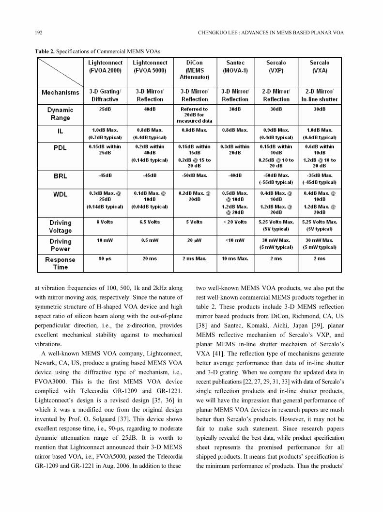
Table 2. Specifications of Commercial MEMS VOAs.
at vibration frequencies of 100, 500, 1k and 2kHz along
with mirror moving axis, respectively. Since the nature of
symmetric structure of H-shaped VOA device and high
aspect ratio of silicon beam along with the out-of-plane
perpendicular direction, i.e., the z-direction, provides
excellent mechanical stability against to mechanical
vibrations.
A well-known MEMS VOA company, Lightconnect,
Newark, CA, US, produce a grating based MEMS VOA
device using the diffractive type of mechanism, i.e.,
FVOA3000. This is the first MEMS VOA device
complied with Telecordia GR-1209 and GR-1221.
Lightconnect’s design is a revised design [35, 36] in
which it was a modified one from the original design
invented by Prof. O. Solgaard [37]. This device shows
excellent response time, i.e., 90-µs, regarding to moderate
dynamic attenuation range of 25dB. It is worth to
mention that Lightconnect announced their 3-D MEMS
mirror based VOA, i.e., FVOA5000, passed the Telecordia
GR-1209 and GR-1221 in Aug. 2006. In addition to these
two well-known MEMS VOA products, we also put the
rest well-known commercial MEMS products together in
table 2. These products include 3-D MEMS reflection
mirror based products from DiCon, Richmond, CA, US
[38] and Santec, Komaki, Aichi, Japan [39], planar
MEMS reflective mechanism of Sercalo’s VXP, and
planar MEMS in-line shutter mechaism of Sercalo’s
VXA [41]. The reflection type of mechanisms generate
better average performance than data of in-line shutter
and 3-D grating. When we compare the updated data in
recent publications [22, 27, 29, 31, 33] with data of Sercalo’s
single reflection products and in-line shutter products,
we will have the impression that general performance of
planar MEMS VOA devices in research papers are mush
better than Sercalo’s products. However, it may not be
fair to make such statement. Since research papers
typically revealed the best data, while product specification
sheet represents the promised performance for all
shipped products. It means that products’ specification is
the minimum performance of products. Thus the products’

JOURNAL OF SEMICONDUCTOR TECHNOLOGY AND SCIENCE, VOL.7, NO.3, SEPTEMBER, 2007 193
specification is generally worse than the best data shown
in research papers. On the other hand, when we check
the data discussed in the multi-channel VOA results in
Ref. [32], we may have equivalent PDL performance for
retro-reflective MEMS VOA and single reflection VOA
of Sercalo’s VXP at 10dB and 20dB attenuation. It
shows the similar data level when we have a large
amount of sampling points. It means these commercial
products are not bad at all. One more interesting point is
the driving voltage. All these commercial products have
the on-chip voltage amplifier except to Santec’s one.
Therefore they all show driving voltage less than or
about 5 volts and response time about 2ms, while
Santec’s one requires driving voltage less than 20 volts
and response time less than 10ms. By leveraging the on-
chip voltage amplifier, these devices can deploy stiffer
springs so as to gain in fast response time, i.e., 2ms.
The aforementioned data point out the promising
application potential of MEMS VOAs. Since the
architecture of next generation optical communication
evolves step by step into the mesh networks from the
present system. New functions and requirements for
MEMS VOAs may come to us upon the network
evolution. The current market demands of MEMS VOAs
already consider as a business of multiple hundred
million US dollars.
ACKNOWLEDGEMENTS
This work was partially supported by grants from a
joint-funded research project based on Faculty Research
Fund R-263-000-358-112/133 of the National University
of Singapore and from the Institute of Microelectronics,
A*Star, Singapore. C. Lee would like to thank his
previous colleagues in Asia Pacific Microsystems, Inc.
for their contribution to some of published works.
REFERENCES
[1] M. C. Wu, O. Solgaard and J. E. Ford, “Optical
MEMS for Lightwave Communication,” J. Ligtwave
Technol., Vol. 24, No. 12, pp.4433-4454, 2006.
[2] J. E. Ford and J. A. Walker, “Dynamic spectral
power equalization using micro-opto-mechanics,”
IEEE Photon. Technol. Lett., Vol.10, No. 10,
pp.1440-1442, 1998.
[3] J. E. Ford, K. W. Goossen, J. A. Walker, D. T.
Neilson, D. M. Tennant, S. Y. Park, and J. W.
Sulhoff, Interference-based micromechanical spectral
equalizers, IEEE J. Sel. Topics Quantum Elect.
Vol. 10, No. 3, pp.579-587, 2004.
[4] J. A. Walker, K. W. Goossen and S. C. Arney,
“Fabrication of a mechanical antireflection switch
for fiber-to-the-home systems,” IEEE J. MEMS,
Vol. 5, No.1, p.45-51, 1996.
[5] J. E. Ford, J. A. Walker, D. S. Greywall and K. W.
Goossen, “Micromechanical fiber-optic attenuator
with 3 µs response,” IEEE J. Lightwave Technol.,
Vol. 16, No. 9, pp. 1663-1670, 1998.
[6] B. Barber, C. R. Giles, V. Askyuk, R. Ruel, L.
Stulz, and D. Bishop, “A fiber connectorized MEMS
variable optical attenuator,” IEEE Photon. Technol.
Lett., Vol. 10, no. 9, pp. 1262-1264, 1998.
[7] C. R. Giles, V. Askyuk, B. Barber, R. Ruel, L.
Stulz, and D. Bishop, “A silicon MEMS optical
switch attenuator and its use in lightwave subsystems,”
IEEE J. Sel. Topics Quantum Elect. Vol. 5, No. 1,
pp.18-25, 1999.
[8] J. A. Walker, “The future of MEMS in
telecommunications networks,” J. Micromech.
Microeng., Vol. 10, pp. R1-R7, 2000.
[9] C. Marxer, P. Griss, and N. F. de Rooij, “A
variable optical attenuator based on silicon
micromechanics,” IEEE Photon. Technol. Lett.,
vol. 11, No.2, pp.233-235, Feb. 1999.
[10] X. M. Zhang, A. Q. Liu, C. Lu and D. Y. Tang,
“MEMS variable optical attenuator using low
driving voltage for DWDM systems,” Electron.
Lett., vol. 38, no. 8, pp. 382-383, 2002.
[11] A. Q. Liu, X. M. Zhang, C. Lu, F. Wang, C. Lu,
and Z. S. Liu, “Optical and mechanical models for
a variable optical attenuator using a micromirror
drawbridge,” J. Micromech. Microeng., vol.13,
pp.400-411, 2003.
[12] X. M. Zhang, A. Q. Liu, C. Lu, F. Wang and Z. S.
Liu, “Polysilicon micromachined fiber-optical
attenuator for DWDM applications,” Sens and
Actuators A, vol.108, pp.28-35, 2003.
[13] C. Lee, Y.-S. Lin, Y.-J. Lai, M. H. Tsai, C. Chen,
and C.-Y. Wu, “3-V driven pop-up micromirror
for reflecting light toward out-of-plane direction
for VOA applications,” IEEE Photon. Technol.
Lett., vol. 16, pp. 1044-1046, Apr. 2004.
194 CHENGKUO LEE : ADVANCES IN MEMS BASED PLANAR VOA
[14] C. Lee and Y.-S. Lin, “A new micromechanism
for transformation of small displacements to large
rotations for a VOA,” IEEE Sensors J., vol. 4, No.
4, pp. 503-509, Aug. 2004.
[15] C. Lee, Y.-J. Lai, C.-Y. Wu, Y.-S. Lin, M. H. Tsai,
R.-S. Huang and M.-S. Lin, “Scratch drive actuator
driven self-assembled variable optical attenuator,”
Jpn. J. Applied Phys., vol. 43, No. 6B, pp. 3906-
3909, 2004.
[16] C. Lee, Y.-J. Lai, C.-Y. Wu, J.A. Yeh, R.-S. Huang,
“Feasibility study of self-assembly mechanism for
variable optical attenuator,” J. Micromech. Microeng.
vol. 15, No.1, pp.55–62, 2005.
[17] C.-H. Kim, N. Park, and Y.-K. Kim, “MEMS
reflective type variable optical attenuator using
off-axis misalignment,” in Proc. IEEE/LEOS Int.
Conf. Optical MEMS 2002, Lugano, Switzerland,
pp. 55–56, Aug. 20–23, 2002.
[18] C. Lee, “Challenges in optical MEMS commercialization
and MEMS foundry,” in IEEE/LEOS Int. Conf.
Optical MEMS 2002, Lugano, Switzerland, Aug.
20–23, 2002, Oral presentation materials.
[19] C. Chen, C. Lee, Y.-J. Lai, and W.-C. Chen,
“Development and application of lateral comb
drive actuator,” Jpn. J. Appl. Phys., pt. 1, vol. 42,
no. 6B, pp. 4067–4073, June 2003.
[20] C. Chen, C. Lee, and Y.-J. Lai, “Novel VOA
using in-plane reflective micromirror and off-axis
light attenuation,” IEEE Commun. Mag., vol. 41,
pp. S16–S20, Aug. 2003.
[21] C.-H. Kim, J. Park, N. Park, and Y.-K. Kim,
“MEMS fiber-optic variable optical attenuator using
collimating lensed fiber,” in Proc. IEEE/LEOS
Intern. Conf. on Optical MEMS 2003, Hawaii,
USA, pp.145-146, Aug. 18-21, 2003.
[22] A. Bashir, P. Katila, N. Ogier, B. Saadany, D. A.
Khalil, “A MEMS-based VOA with very low PDL,”
IEEE Photon. Technol. Lett., Vol.16, No. 4, pp.
1047-1049, Apr. 2004.
[23] T.-S. Lim, C.-H. Ji, C.-H. Oh, Y. Yee and J. U. Bu,
“Electrostatic MEMS variable optical attenuator
with folded micromirror,” in Proc. IEEE/LEOS Intern.
Conf. on Optical MEMS 2003, Hawaii, USA,
pp.143-144, Aug. 18-21, 2003.
[24] C. Lee, M. H. Tsai, C.-Y. Wu, S.-Y. Hung, C.
Chen, Y.-J. Lai, M.-S. Lin, and J. Andrew Yeh,
“Characterization of MOEMS VOA Based on
Various Planar Light Attenuation Configurations,”
in Proc. of IEEE/LEOS International Conf. on
Optical MEMS 2004, Takamtsu, Japan, pp.98-99,
Aug. 22-26, 2004.
[25] C. Chen, C. Lee and J. Andrew Yeh, “Retro-
Reflection Type MOEMS VOA,” IEEE Photonics
Tech. Letters, Vol. 16, No. 10, pp. 2290-2292, Oct.
2004.
[26] T.-S. Lim, C.-H. Ji, C.-H. Oh, H. Kwon, Y. Yee,
and J. U. Bu, “ Electrostatic MEMS variable
optical attenuator with rotating folded micromirror,”
IEEE J. Sel. Topics Quantum Elect., Vol.10, pp.
558-562, May/June 2004.
[27] J. A. Yeh, S.-S. Jiang and C. Lee, “MOEMS VOA
Using Rotary Comb Drive Actuators,” Vol. 18,
No. 10, pp. 1170-1172, May 15, 2006.
[28] Y. Y. Kim, S. S. Yun, C. S. Park, J.-H. Lee, Y. G.
Lee, H. K. Lee, S. K. Yoon and J. S. Kang,
“Refractive variable optical attenuator fabricated
by silicon deep reactive ion etching,” IEEE Photon.
Technol. Lett., Vol.16, No. 2, pp.485-487, Apr.
2004.
[29] C.-H. Kim and Y.-K. Kim, “MEMS variable
optical attenuator using translation motion of 45º
tilted vertical mirror,” J. Micromech. Microeng.,
vol.15, pp. 1466-1475, 2005.
[30] H. Cai, X. M. Zhang, C. Lu, A. Q. Liu , and E. H.
Khoo, “ Linear MEMS variable optical attenuator
using reflective elliptical mirror,” IEEE Photon.
Technol. Lett., vol. 17, No.2, pp. 402-404, Feb. 2005.
[31] C. Lee, “Monolithic-integrated 8CH MEMS variable
optical attenuators,” Sens and Actuators A, vol.
123-124, pp.596-601, 2005.
[32] C. Lee, “Arrayed Variable Optical Attenuator Using
Retro-Reflective MEMS Mirrors,” IEEE Photon.
Technol. Lett., vol. 17, No. 12, pp. 2640-2642, Dec.
2005.
[33] C. Lee, “MOEMS Variable Optical Attenuator with
Robust Design for Improved Dynamic Characteristics,”
IEEE Photonics Tech. Letters, vol. 18, No. 6, pp.
773-775, Mar. 15, 2006.
[34] C. Lee, “A MEMS VOA Using Electrothermal
Actuators,” IEEE J. Lightwave Technol., vol. 25,
No.2, pp.490-498, Feb. 2007.
[35] A. Godil, “Diffractive MEMS technology offers a

JOURNAL OF SEMICONDUCTOR TECHNOLOGY AND SCIENCE, VOL.7, NO.3, SEPTEMBER, 2007 195
new platform for optical networks,” Laser Focus
World, 38(5), 181–185, (2002).
[36] http://www.lightconnect.com/
[37] O. Solgaard, F. S. A. Sandejas, and D. M. Bloom,
“Deformable grating optical modulator,” Opt. Lett.,
17(9), 688–690, (1992).
[38] http://www.diconfiberoptics.com/
[39] http://www.santec.com/
[40] http://www.sercalo.com/
Chenkuo Lee received a M.S.
degree in Materials Science and
Engineering from National Tsing
Hua University, Hsinchu, Taiwan, in
1991. He also received a M.S.
degree in Industrial and System
Engineering from Rutgers University, New Brunswick,
NJ, USA in 1993. He received the Ph.D. degree in
Precision Engineering from the University of Tokyo,
Tokyo, Japan, in Jan. 1996. He worked as foreign
researcher in the Nanometer-scale Manufacturing
Science Lab. at Research Center for Advanced Science
and Technology (RCAST) of the University of Tokyo
from 1993 to 1996. He had also worked in Mechanical
Engineering Lab., AIST, MITI of Japan as a JST
research fellow in 1996. Thereafter he was a senior
research staff of Microsystems Lab., Industrial
Technology Research Institute (ITRI), Hsinchu, Taiwan.
Since Sept. 1997, he has joined the Metrodyne
Microsystem Corporation, Hsinchu, Taiwan, and
established the MEMS device division and the 1st
micromachining fab for commercial purpose in Taiwan.
He was the manager of MEMS device division between
1997 and 2000. He had been the adjunct assistant
professor in Electro-physics Department of National
Chiao Tung University in 1998, and the adjunct assistant
professor in Institute of Precision Eng. of National
Chung Hsing University since 2001 to 2005. He co-
founded the Asia Pacific Microsystems, Inc. (APM)
Hsinchu, Taiwan, in Aug. 2001, and he has been the vice
president at APM, Inc. till end of 2005. APM was
ranked as one of the top 30 MEMS manufacturers in the
world in recent years. Currently He is an assistant
professor at the Dept. of Electrical and Computer Eng.
of National University of Singapore and a senior
member of technical staff at the Institute of
Microelectronics (IME), A*STAR, Singapore. He has
contributed more than 80 international conference
papers and extended abstracts, 45 peer-reviewed
international journal articles, and 8 US patents in MEMS
and Nanotechnology field. He is the member of IEEE,
MRS, and IEE Japan.
Ruey Shing Huang received his
Ph.D. from the University of New
South Wales, Sydney, Australia in
1979. He then joined National Tsing
Hua University as Associated Professor
in the department of electrical
engineering, and became full Professor and Chairman of
the department in 1984. In 1986 Dr. Huang moved to
Australia and became a faculty member of the school of
electrical engineering, the University of New South
Wales until 1994. He rejoined National Tsing Hua
University since 1994 and served as the head of the
department from 1997 to 2000. A pioneer of MEMS
research in Taiwan, Dr. Huang initiated and managed
the MEMS program for National Science Council and as
the director of the Center Regional MEMS Research
Center. In 2001, he co-founded Asia Pacific
Microsystems, Inc., a dedicate MEMS manufacturing
company. Since then he has been the chief technology
officer (CTO) at APM, Inc. Dr. Huang’s research was in
the sub-micron technology for microelectronics and later
in micro-fabrication for sensors and MEMS. He has
published numerous papers and holds several patents.


![1. VOA Capacity Cover...1. VOA Capacity Cover [VOA] Optimize Capacity vSphere World 2. VOA Capacity Overview [VOA] Optimize Capacity 3. VOA Report Capacity Overview [VOA] Optimize](https://static.fdocuments.us/doc/165x107/5f78a190994efe06a97a414b/1-voa-capacity-cover-1-voa-capacity-cover-voa-optimize-capacity-vsphere.jpg)