Advanced x86: BIOS and System Management Mode Internals PCI Xeno Kovah && Corey Kallenberg...
54
Advanced x86: BIOS and System Management Mode Internals PCI Xeno Kovah && Corey Kallenberg LegbaCore, LLC
-
Upload
shana-kennedy -
Category
Documents
-
view
244 -
download
6
Transcript of Advanced x86: BIOS and System Management Mode Internals PCI Xeno Kovah && Corey Kallenberg...
Advanced x86:BIOS and System Management Mode Internals
PCI
Xeno Kovah && Corey KallenbergLegbaCore, LLC
All materials are licensed under a Creative Commons “Share Alike” license.
http://creativecommons.org/licenses/by-sa/3.0/
2Attribution condition: You must indicate that derivative work"Is derived from John Butterworth & Xeno Kovah’s ’Advanced Intel x86: BIOS and SMM’ class posted at http://opensecuritytraining.info/IntroBIOS.html”
PCI (and PCI Express)
All your base. base. base…all your base address registers are
belong to PCI
PCI note:
• We’re not really going to care about low level PCI protocol details
• We’re just going to care about the way that it’s exposed to the BIOS, so that we can understand the BIOS’s view of the world, and therefore interpret its actions accordingly
• If you care about the physical level details, you need to go out and get a big ol’ book (like the full version of this https://www.mindshare.com/files/ebooks/PCI%20Express%20System%20Architecture.pdf)
4
PCI• Peripheral Component Interconnect (PCI)
– Also called Compatible PCI
• It’s a bus protocol developed by Intel around 1993• Purpose is to attach/interconnect local hardware devices to a computer• PCI is integrated into the chipset, forming a “backbone”
– Holds true for both Intel and AMD-based systems– Logically speaking, the Chipset is a PCI System
• 32-bit bus with multiplexed address and data lines– Supports 64-bit by performing two 32-bit reads
• PCI component interface is processor independent– The CPU/BIOS reads and writes to the configuration space to configure much of
the system
• Intel’s MCH/ICH chipsets implement PCI Local Bus Protocol 2.3• PCH chipsets implement PCI Express protocol (v. 2.0)
– Still supports PCI 2.3
• PCI standards are currently maintained and defined by the PCI /SIG:– http://www.pcisig.com/specifications/
5
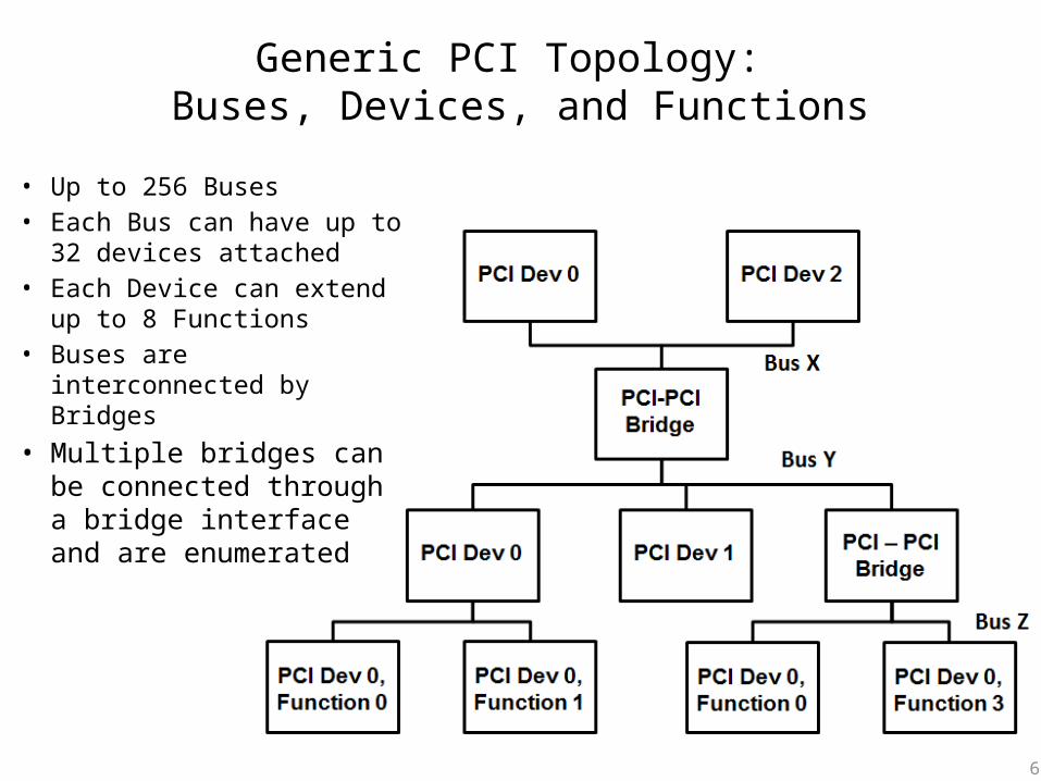
Generic PCI Topology: Buses, Devices, and Functions
• Up to 256 Buses• Each Bus can have up to
32 devices attached• Each Device can extend
up to 8 Functions• Buses are interconnected
by Bridges
• Multiple bridges can be connected through a bridge interface and are enumerated
6
PCI Address Spaces
• PCI implements three address spaces:
• 1) PCI Configuration Space (up to 256 Bytes)– Required/standard. Defined in the specifications. Every PCI device has
a configuration space.
• 2) PCI Memory-mapped space– Optional. Dependent on whether the device manufacturer needs to map
system memory to the PCI device
• 3) PCI I/O-mapped space– Optional. Same as PCI Memory Space
7
PCI Express (PCIe)
• Peripheral Component Interconnect Express (PCIe)• Developed around 2004 (not just by Intel but a collective)• Packet-based transaction protocol• Very different from PCI at the hardware level• For software configuration purposes, it is mostly the same
– Adds an extended configuration space of 4KB
• Provides backwards compatibility for Compatible PCI• Adds 4KB of PCI Express Extended Capabilities
registers – Located in either the Configuration space starting at offset 256
(immediately following the Compatible PCI configuration space)– Or located at a MMIO location specified in the Root Complex
Register Block (RCRB)
8
PCI Express (PCIe) Address Spaces
• PCIe implements four address spaces:
• 1) PCIe Configuration Space (up to 4KBytes)– Required/standard. Defined in the specifications. Every PCIe device has
its configuration space mapped to memory. – Also provides the first 256 bytes of compatible PCI (memory-mapped
and via port IO for backwards compatibility)
• 2) PCIe Memory-mapped space– Optional. Dependent on whether the device manufacturer needs to map
system memory to the PCI device
• 3) PCIe I/O-mapped space– Optional. Same as PCI Memory Space
• 4) PCIe Message Space– For low-level protocol messaging/interrupts. We don’t get into this in this
class
9
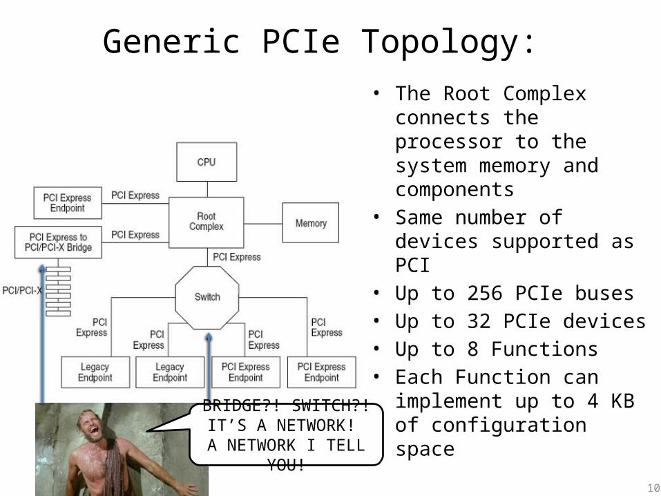
Generic PCIe Topology:
• The Root Complex connects the processor to the system memory and components
• Same number of devices supported as PCI
• Up to 256 PCIe buses• Up to 32 PCIe devices• Up to 8 Functions• Each Function can
implement up to 4 KB of configuration space
10
BRIDGE?! SWITCH?!IT’S A NETWORK!
A NETWORK I TELL YOU!
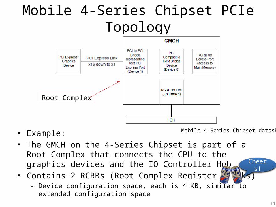
• Example:• The GMCH on the 4-Series Chipset is part of a Root Complex
that connects the CPU to the graphics devices and the IO Controller Hub
• Contains 2 RCRBs (Root Complex Register Blocks) – Device configuration space, each is 4 KB, similar to extended
configuration space
Mobile 4-Series Chipset PCIe Topology
Mobile 4-Series Chipset datasheet
Root Complex
11
Cheers!
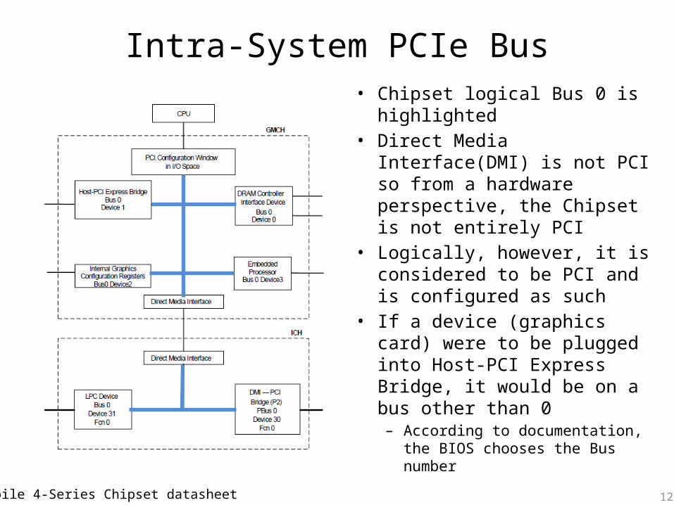
• Chipset logical Bus 0 is highlighted
• Direct Media Interface(DMI) is not PCI so from a hardware perspective, the Chipset is not entirely PCI
• Logically, however, it is considered to be PCI and is configured as such
• If a device (graphics card) were to be plugged into Host-PCI Express Bridge, it would be on a bus other than 0– According to documentation,
the BIOS chooses the Bus number
Intra-System PCIe Bus
Mobile 4-Series Chipset datasheet 12
Configuration Space Accesses• There are two ways to access the compatible PCI configuration
space registers (0 to 255)…– Port IO or Memory-mapped IO
• …but only one way to access the extended configuration space offered by PCI Express (255 to 4KB)– Memory-mapped IO
• Generally speaking, you will see accesses to PCI being performed via Port I/O in a couple situations:– When in Real Mode when accesses to 32-bit memory space is limited
• Real Mode may be reentered even after the system has transitioned to Protected mode (up to the vendor and their implementation, flat real mode could pull it off)
• I have only seen this done in a Legacy BIOS, never in UEFI
– Before PCIEXBAR has been configured• Cause it enables MMIO
• Outside of those situations, you’ll probably see PCI accesses performed via memory-mapped I/O
• But of course this is all up to the developers 13
Compatible PCI Configuration Space• This refers to the software generation of PCI configuration
transactions– those generated by the CPU/BIOS
• Compatible PCI provides 256 bytes of Configuration address space to the CPU/BIOS
• CPU/BIOS programs the registers contained therein to configure the device and system parameters
• Compatible PCI is configured using the port I/O address/data pair (CONFIG_ADDRESS, CONFIG_DATA)
• Two 32-bit I/O locations are used to generate configuration transactions– CF8h (CONFIG_ADDRESS)– CFCh (CONFIG_DATA)
• Curiously, these are never listed in the Fixed IO Address space registers in the applicable chipset datasheets, but are explicitly mentioned as CF8/CFC in the datasheets 14
I/O Port CONFIG_ADDRESS (CF8h)
• 32 bits (GIMME BUS 0, DEVICE 31 (0x1F), Function 0, offset 0x88)• Port CF8h• Bit 31 when set, all reads and writes to CONFIG_DATA are PCI
Configuration transactions • Bits 30:24 are read-only and must return 0 when read• Bits 23:16 select a specific Bus in the system (up to 256 buses)• Bits 15:11 specify a Device on the given Bus (up to 32 devices)• Bits 10:8 Specify the function of a device (up to 8 devices)• Bits 7:0 Select an offset within the Configuration Space (256 bytes max,
DWORD-aligned as bits 1:0 are hard-coded 0)• Addresses are often given in B/D/F, Offset notation (also written as B:D:F,
Offset) 15
B D F Offset
I/O Port CONFIG_ADDRESS (CF8h)
• THIS IS KEY!• YOU MUST UNDERSTAND THIS!
16
B D F Offset
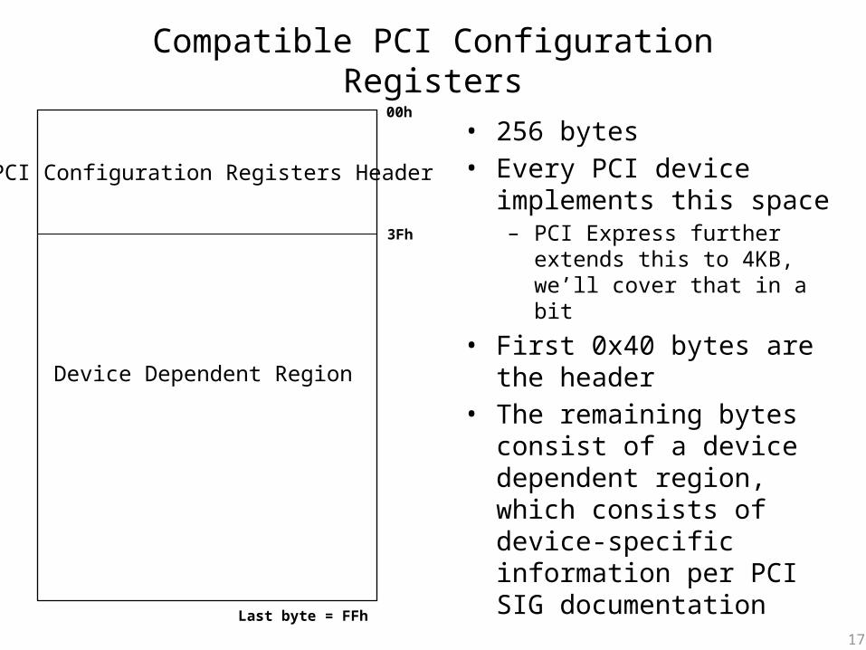
Compatible PCI Configuration Registers
• 256 bytes • Every PCI device
implements this space– PCI Express further extends
this to 4KB, we’ll cover that in a bit
• First 0x40 bytes are the header
• The remaining bytes consist of a device dependent region, which consists of device-specific information per PCI SIG documentation
PCI Configuration Registers Header
00h
3Fh
Device Dependent Region
17
Last byte = FFh
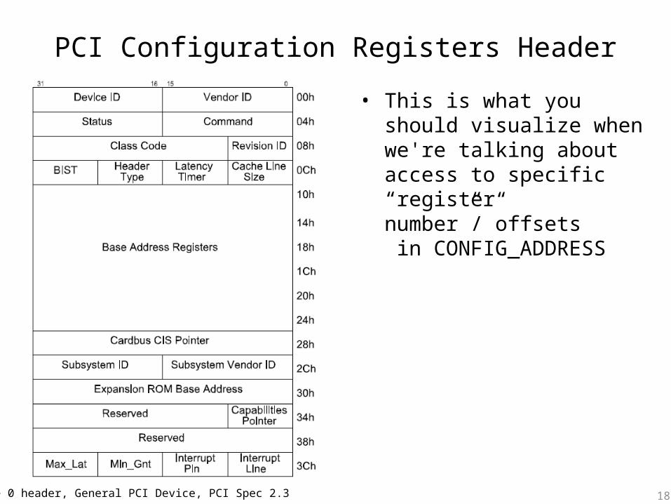
PCI Configuration Registers Header
• This is what you should visualize when we're talking about access to specific “register number”/”offsets in CONFIG_ADDRESS
Type 0 header, General PCI Device, PCI Spec 2.3 18
I/O Port CONFIG_DATA (CFCh)
• CONFIG_DATA can be accessed in DWORD, WORD, or BYTE configurations
• Reads and Writes to CONFIG_DATA with Bit 31 in CONFIG_ADDRESS set/enabled results in a PCI Configuration transaction to the device specified in CONFIG_ADDRESS
• PCI spec says that if Bit 31 is not enabled, then the transaction is forwarded out as Port I/O
19
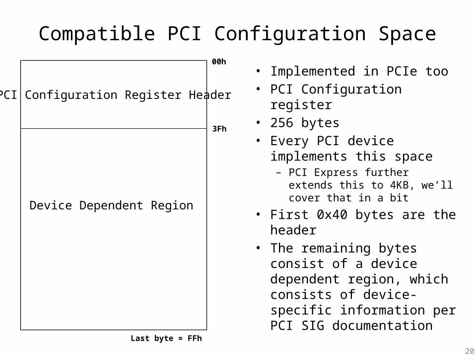
Compatible PCI Configuration Space
• Implemented in PCIe too• PCI Configuration register • 256 bytes • Every PCI device
implements this space– PCI Express further extends
this to 4KB, we’ll cover that in a bit
• First 0x40 bytes are the header
• The remaining bytes consist of a device dependent region, which consists of device-specific information per PCI SIG documentation
PCI Configuration Register Header
00h
3Fh
Last byte = FFh
Device Dependent Region
20
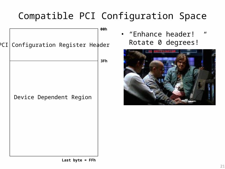
Compatible PCI Configuration Space
• “Enhance header! Rotate 0 degrees!”PCI Configuration Register Header
00h
3Fh
Device Dependent Region
21
Last byte = FFh
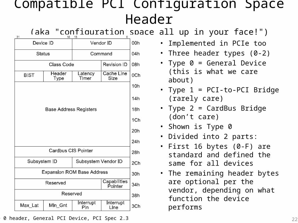
Compatible PCI Configuration Space Header(aka "configuration space all up in your face!")
• Implemented in PCIe too• Three header types (0-2)• Type 0 = General Device (this is
what we care about)• Type 1 = PCI-to-PCI Bridge
(rarely care)• Type 2 = CardBus Bridge (don’t
care)• Shown is Type 0• Divided into 2 parts:• First 16 bytes (0-F) are
standard and defined the same for all devices
• The remaining header bytes are optional per the vendor, depending on what function the device performs
Type 0 header, General PCI Device, PCI Spec 2.3 22
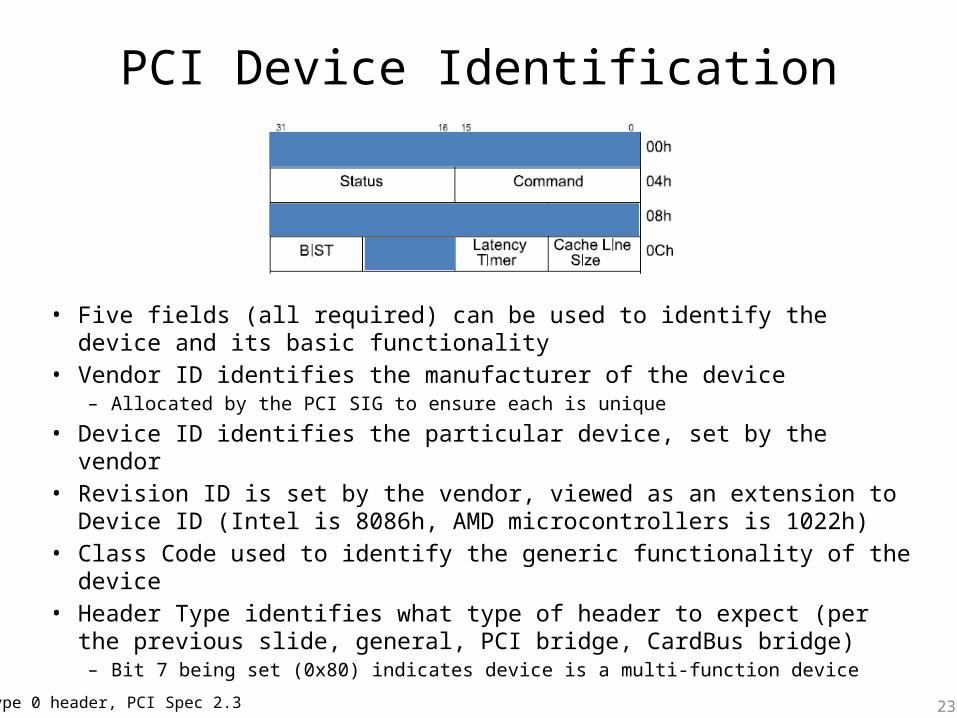
PCI Device Identification
• Five fields (all required) can be used to identify the device and its basic functionality
• Vendor ID identifies the manufacturer of the device– Allocated by the PCI SIG to ensure each is unique
• Device ID identifies the particular device, set by the vendor• Revision ID is set by the vendor, viewed as an extension to Device ID
(Intel is 8086h, AMD microcontrollers is 1022h)• Class Code used to identify the generic functionality of the device • Header Type identifies what type of header to expect (per the
previous slide, general, PCI bridge, CardBus bridge)– Bit 7 being set (0x80) indicates device is a multi-function device
Type 0 header, PCI Spec 2.3 23
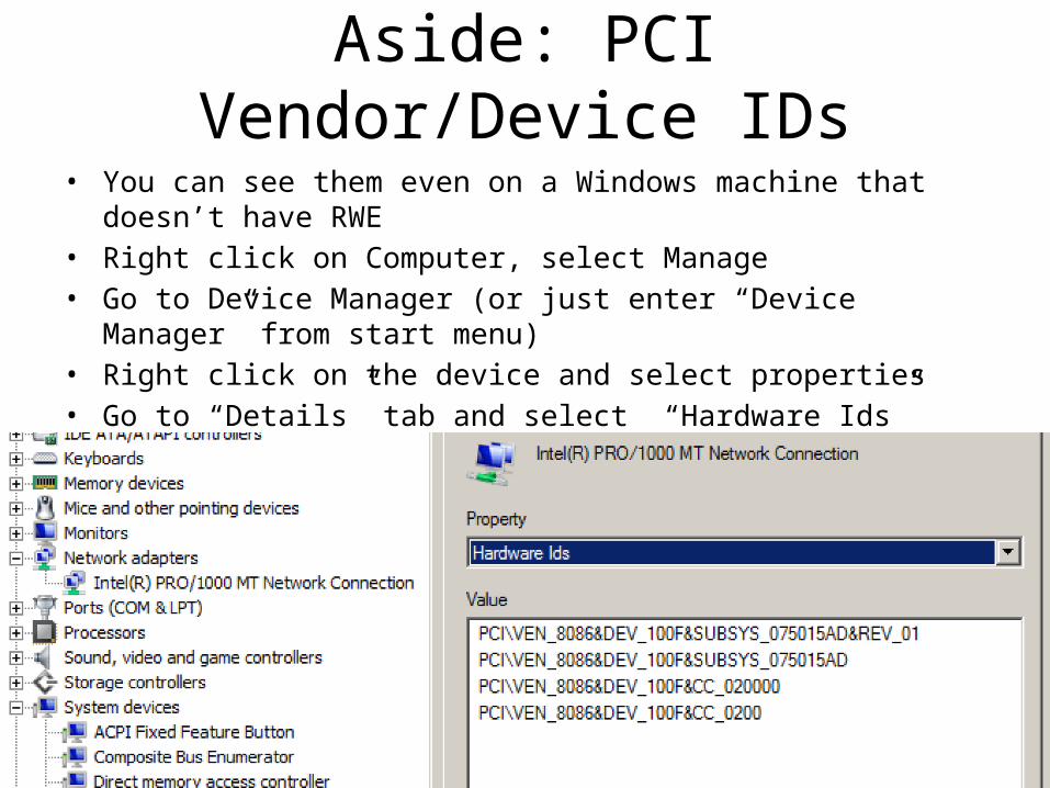
Aside: PCI Vendor/Device IDs• You can see them even on a Windows machine that doesn’t have RWE• Right click on Computer, select Manage• Go to Device Manager (or just enter “Device Manager” from start menu)• Right click on the device and select properties• Go to “Details” tab and select “Hardware Ids”
24
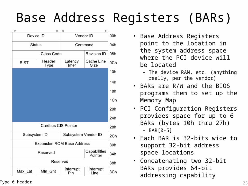
Base Address Registers (BARs)• Base Address Registers point to
the location in the system address space where the PCI device will be located– The device RAM, etc. (anything
really, per the vendor)
• BARs are R/W and the BIOS programs them to set up the Memory Map
• PCI Configuration Registers provides space for up to 6 BARs (bytes 10h thru 27h)– BAR[0-5]
• Each BAR is 32-bits wide to support 32-bit address space locations
• Concatenating two 32-bit BARs provides 64-bit addressing capability Type 0 header 25
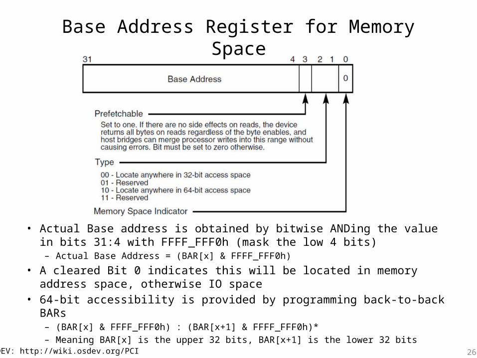
• Actual Base address is obtained by bitwise ANDing the value in bits 31:4 with FFFF_FFF0h (mask the low 4 bits)– Actual Base Address = (BAR[x] & FFFF_FFF0h)
• A cleared Bit 0 indicates this will be located in memory address space, otherwise IO space
• 64-bit accessibility is provided by programming back-to-back BARs– (BAR[x] & FFFF_FFF0h) : (BAR[x+1] & FFFF_FFF0h)*– Meaning BAR[x] is the upper 32 bits, BAR[x+1] is the lower 32 bits
Base Address Register for Memory Space
*OSDEV: http://wiki.osdev.org/PCI 26
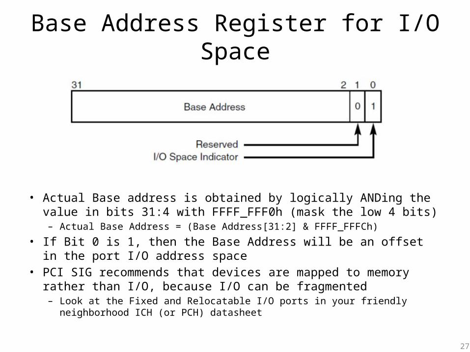
Base Address Register for I/O Space
• Actual Base address is obtained by logically ANDing the value in bits 31:4 with FFFF_FFF0h (mask the low 4 bits)– Actual Base Address = (Base Address[31:2] & FFFF_FFFCh)
• If Bit 0 is 1, then the Base Address will be an offset in the port I/O address space
• PCI SIG recommends that devices are mapped to memory rather than I/O, because I/O can be fragmented – Look at the Fixed and Relocatable I/O ports in your friendly neighborhood ICH
(or PCH) datasheet
27
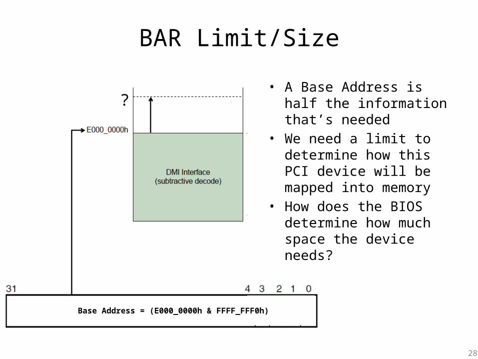
BAR Limit/Size
• A Base Address is half the information that’s needed
• We need a limit to determine how this PCI device will be mapped into memory
• How does the BIOS determine how much space the device needs?
?
Base Address = (E000_0000h & FFFF_FFF0h)
28
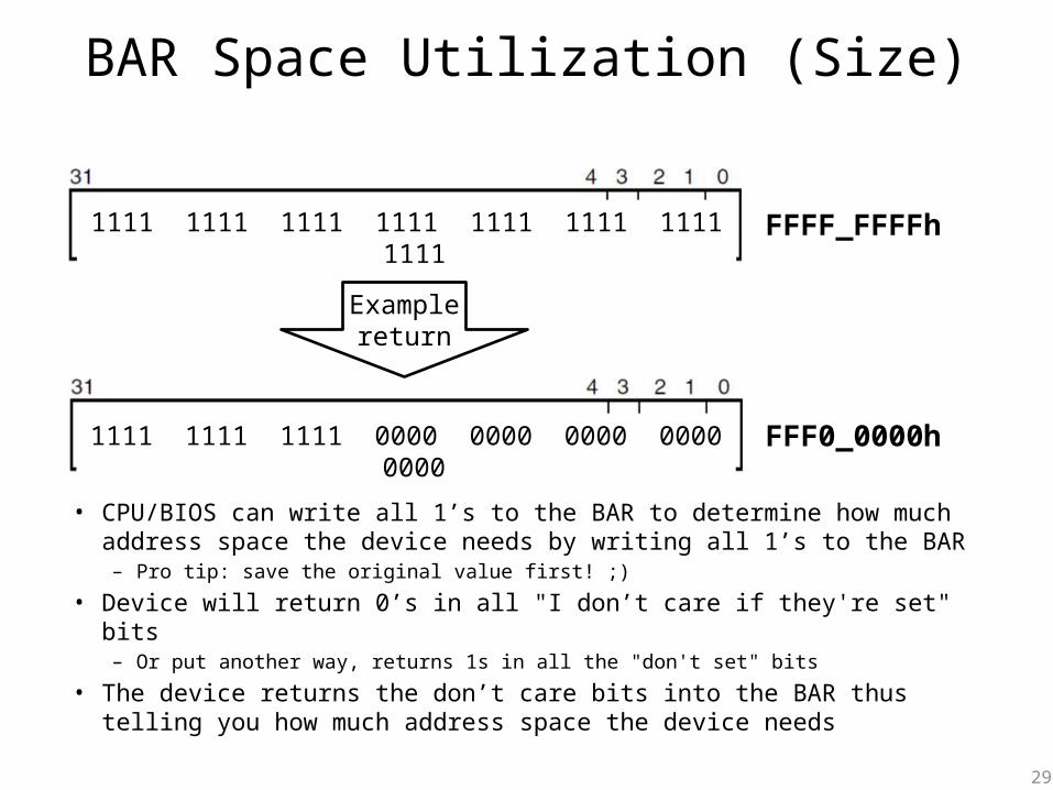
BAR Space Utilization (Size)
• CPU/BIOS can write all 1’s to the BAR to determine how much address space the device needs by writing all 1’s to the BAR– Pro tip: save the original value first! ;)
• Device will return 0’s in all "I don’t care if they're set" bits– Or put another way, returns 1s in all the "don't set" bits
• The device returns the don’t care bits into the BAR thus telling you how much address space the device needs
1111 1111 1111 1111 1111 1111 1111 1111
1111 1111 1111 0000 0000 0000 0000 0000
Examplereturn
FFFF_FFFFh
FFF0_0000h
29
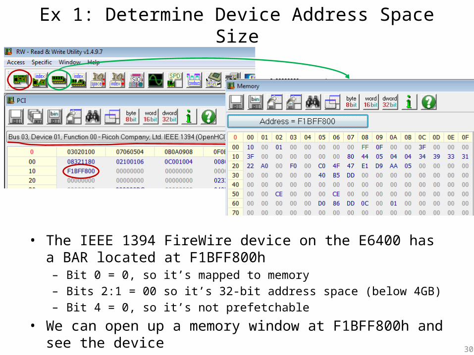
Ex 1: Determine Device Address Space Size
• The IEEE 1394 FireWire device on the E6400 has a BAR located at F1BFF800h– Bit 0 = 0, so it’s mapped to memory– Bits 2:1 = 00 so it’s 32-bit address space (below 4GB)– Bit 4 = 0, so it’s not prefetchable
• We can open up a memory window at F1BFF800h and see the device 30
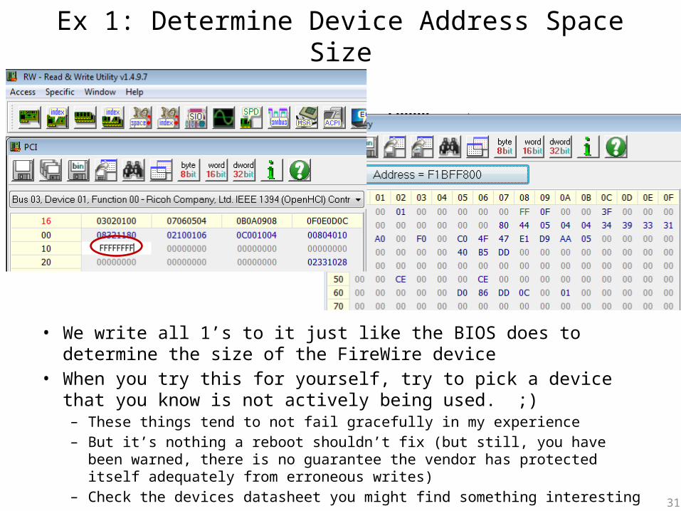
Ex 1: Determine Device Address Space Size
• We write all 1’s to it just like the BIOS does to determine the size of the FireWire device
• When you try this for yourself, try to pick a device that you know is not actively being used. ;)– These things tend to not fail gracefully in my experience– But it’s nothing a reboot shouldn’t fix (but still, you have been warned, there is no
guarantee the vendor has protected itself adequately from erroneous writes) – Check the devices datasheet you might find something interesting
31
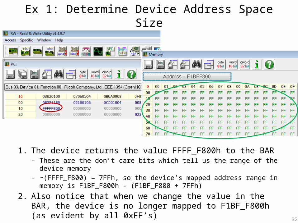
Ex 1: Determine Device Address Space Size
1. The device returns the value FFFF_F800h to the BAR– These are the don’t care bits which tell us the range of the device memory– ~(FFFF_F800) = 7FFh, so the device’s mapped address range in memory
is F1BF_F800h - (F1BF_F800 + 7FFh)
2. Also notice that when we change the value in the BAR, the device is no longer mapped to F1BF_F800h (as evident by all 0xFF’s)
32
Ex 1: Determine Device Address Space Size
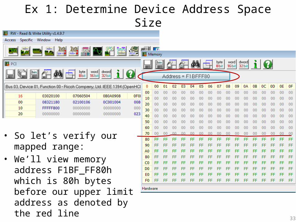
• So let’s verify our mapped range:
• We’ll view memory address F1BF_FF80h which is 80h bytes before our upper limit address as denoted by the red line
33
Ex 1: Determine Device Address Space Size
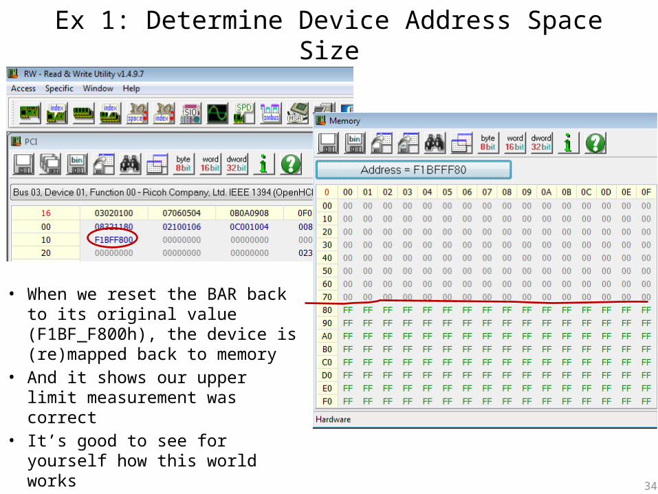
• When we reset the BAR back to its original value (F1BF_F800h), the device is (re)mapped back to memory
• And it shows our upper limit measurement was correct
• It’s good to see for yourself how this world works
34
Ex 2: Relocate the PCI Device Mapping
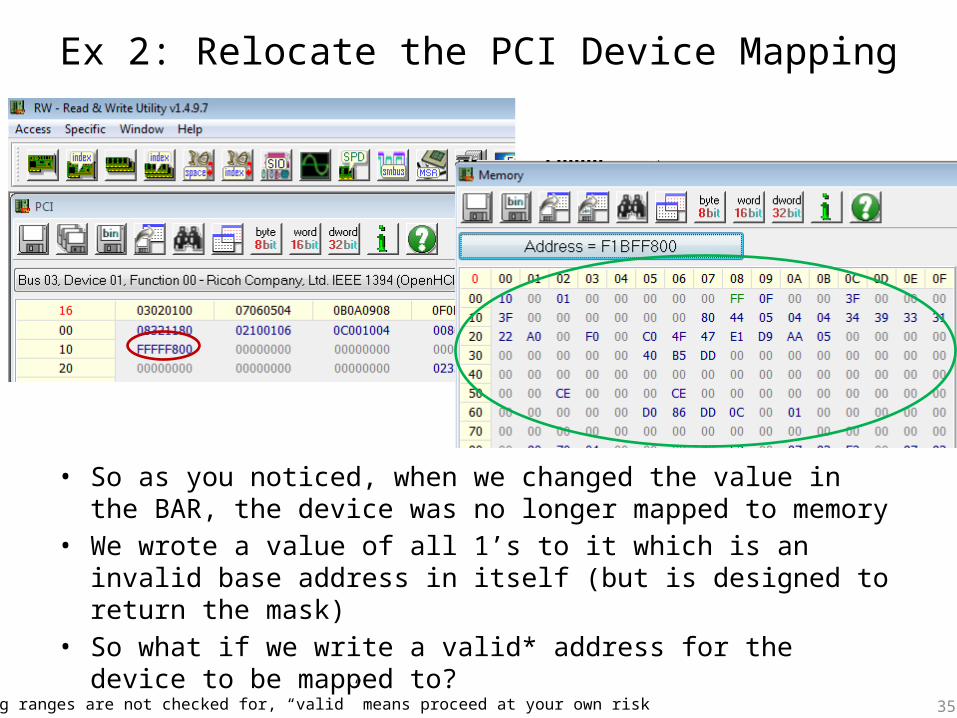
• So as you noticed, when we changed the value in the BAR, the device was no longer mapped to memory
• We wrote a value of all 1’s to it which is an invalid base address in itself (but is designed to return the mask)
• So what if we write a valid* address for the device to be mapped to?
*Overlapping ranges are not checked for, “valid” means proceed at your own risk 35
Ex 2: Relocate the PCI Device Mapping
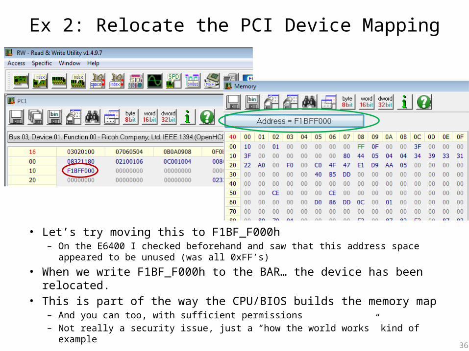
• Let’s try moving this to F1BF_F000h– On the E6400 I checked beforehand and saw that this address space
appeared to be unused (was all 0xFF’s)
• When we write F1BF_F000h to the BAR… the device has been relocated.
• This is part of the way the CPU/BIOS builds the memory map– And you can too, with sufficient permissions– Not really a security issue, just a “how the world works” kind of example 36

Aside: Things to be aware of once you start learning down at this level
• Here's a recent ASIA CCS paper evaluating whether past work on attacks that manipulate PCI (e.g. forcing MMIO overlap, configuration range overlap, etc) and other low level information for a pass-through device inside virtual environments (answer: doesn't seem like it, but they found a new attack :))
• On the Feasibility of Software Attacks on Commodity Virtual Machine Monitors via Direct Device Assignment – Pek et al.
• https://www.iseclab.org/people/andrew/download/asia14.pdf
37
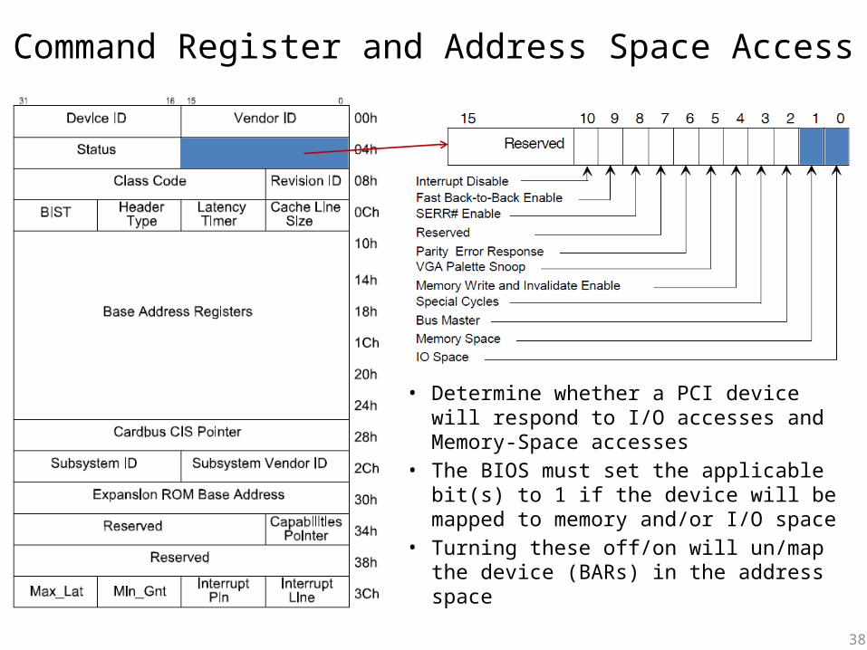
Command Register and Address Space Access
• Determine whether a PCI device will respond to I/O accesses and Memory-Space accesses
• The BIOS must set the applicable bit(s) to 1 if the device will be mapped to memory and/or I/O space
• Turning these off/on will un/map the device (BARs) in the address space
38
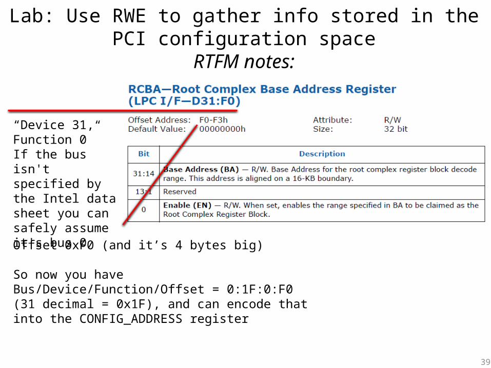
Lab: Use RWE to gather info stored in the PCI configuration space
RTFM notes:
39
“Device 31, Function 0”If the bus isn't specified by the Intel data sheet you can safely assume it's bus 0
Offset 0xF0 (and it’s 4 bytes big)
So now you have Bus/Device/Function/Offset = 0:1F:0:F0 (31 decimal = 0x1F), and can encode that into the CONFIG_ADDRESS register
Lab: Use RWE to gather info stored in the PCI configuration space
• Let’s find the RCRB address, since we’ll be using it to get to the SPI flash interface– Refer to your datasheet if doing on your own system but it should be at
B0:D31:F0 (LPC device), offset F0h
40
This association is highly refreshing!
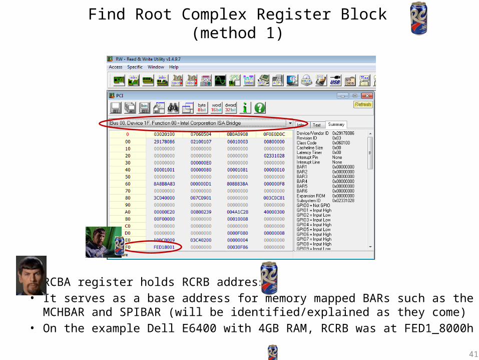
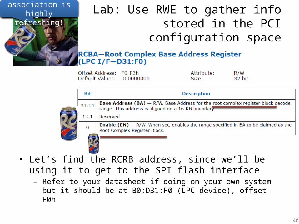
Find Root Complex Register Block(method 1)
• RCBA register holds RCRB address• It serves as a base address for memory mapped BARs such as the
MCHBAR and SPIBAR (will be identified/explained as they come)• On the example Dell E6400 with 4GB RAM, RCRB was at FED1_8000h
41
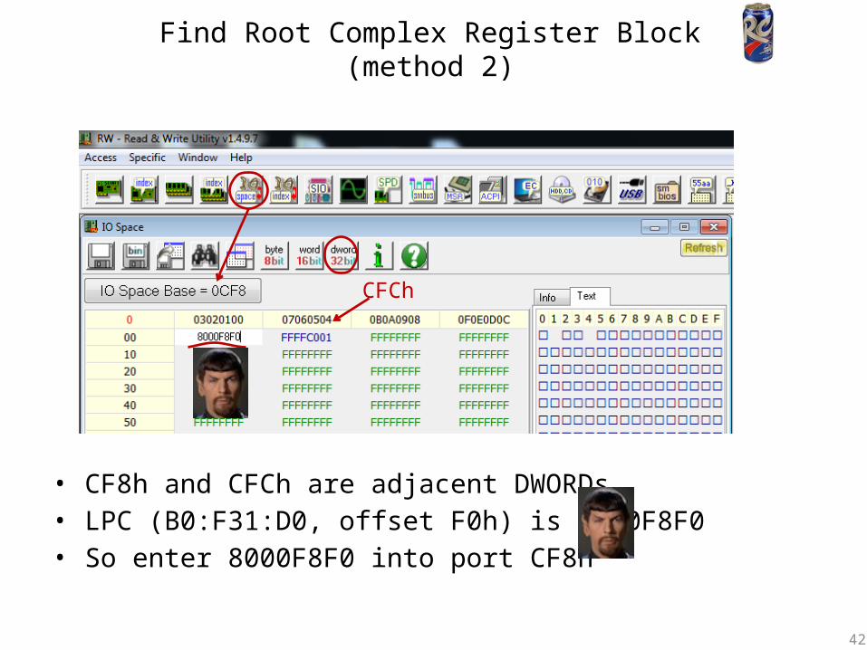
• CF8h and CFCh are adjacent DWORDs• LPC (B0:F31:D0, offset F0h) is 8000F8F0• So enter 8000F8F0 into port CF8h
CFCh
42
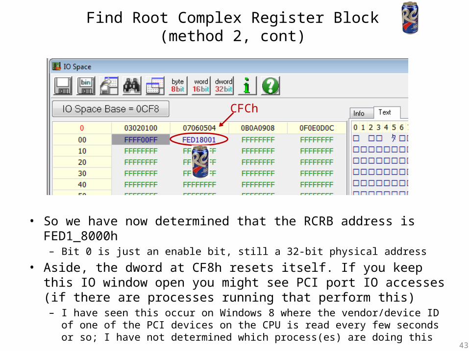
Find Root Complex Register Block(method 2)
Find Root Complex Register Block(method 2, cont)
• So we have now determined that the RCRB address is FED1_8000h– Bit 0 is just an enable bit, still a 32-bit physical address
• Aside, the dword at CF8h resets itself. If you keep this IO window open you might see PCI port IO accesses (if there are processes running that perform this)– I have seen this occur on Windows 8 where the vendor/device ID of one of the
PCI devices on the CPU is read every few seconds or so; I have not determined which process(es) are doing this
CFCh
43
PCI vs. PCIe config space access
44
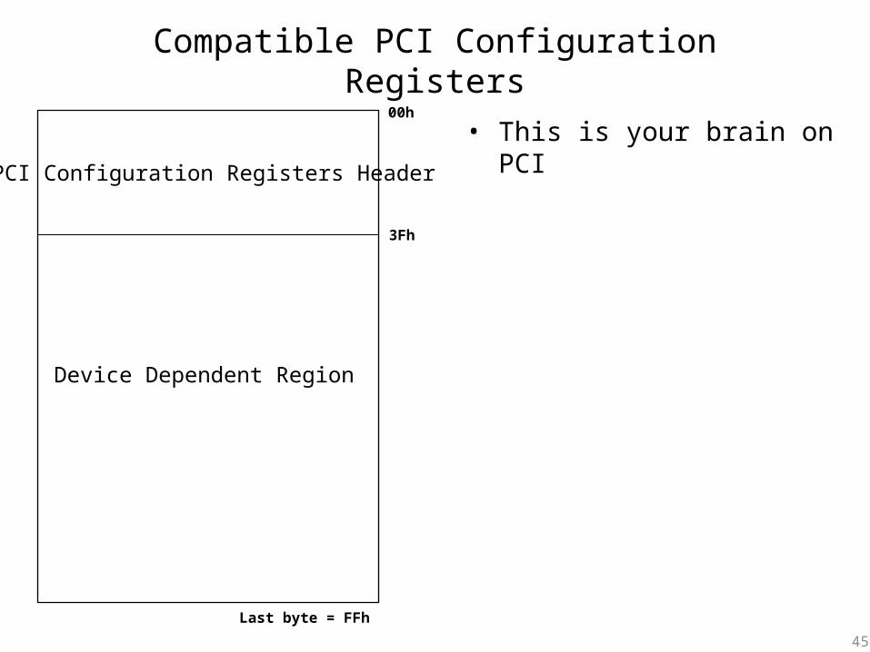
Compatible PCI Configuration Registers
• This is your brain on PCI
PCI Configuration Registers Header
00h
3Fh
Device Dependent Region
45
Last byte = FFh
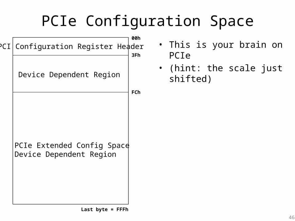
PCIe Configuration Space
• This is your brain on PCIe• (hint: the scale just shifted)
PCI Configuration Register Header00h
3Fh
FCh
Device Dependent Region
46
PCIe Extended Config SpaceDevice Dependent Region
Last byte = FFFh
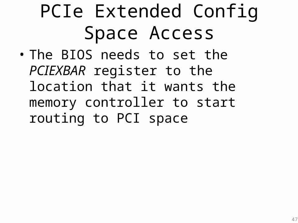
PCIe Extended Config Space Access
• The BIOS needs to set the PCIEXBAR register to the location that it wants the memory controller to start routing to PCI space
47
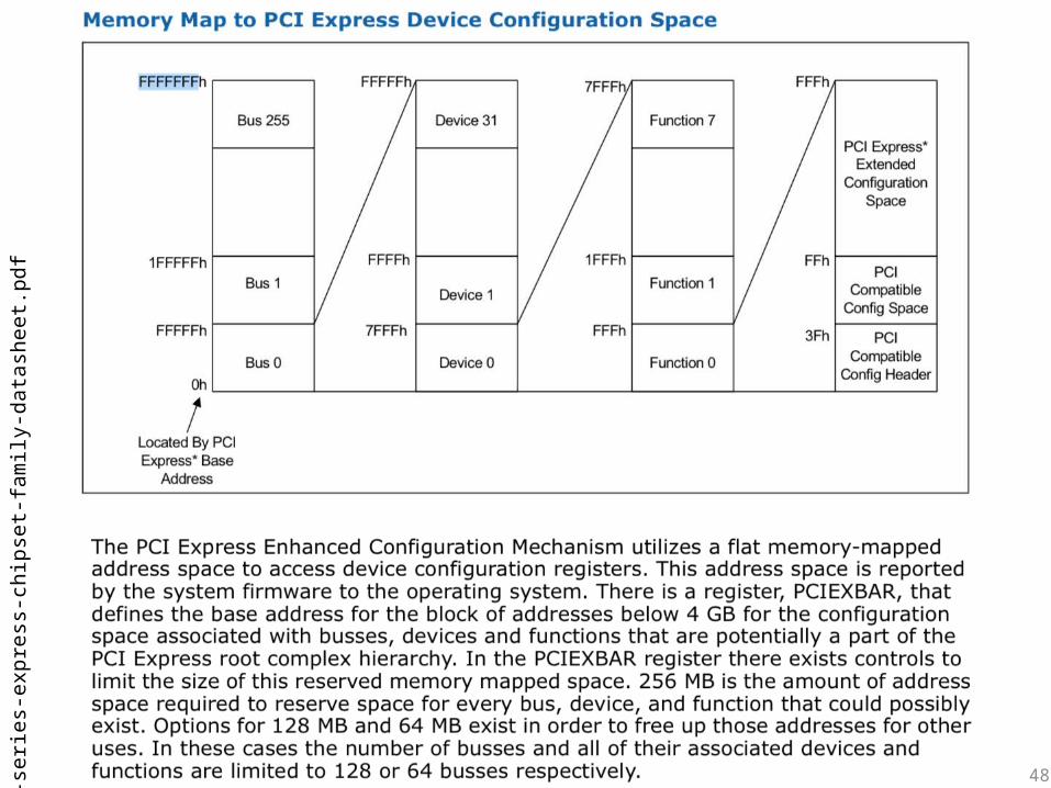
48From
3-s
erie
s-ex
pres
s-ch
ipse
t-fam
ily-d
atas
heet
PCIe Memory-Mapped Config Space Access
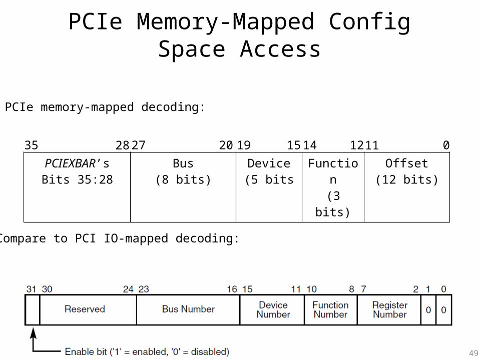
49
PCIEXBAR’sBits 35:28
Bus(8 bits)
Device(5 bits
Function(3 bits)
Offset(12 bits)
0111214151920272835
PCIe memory-mapped decoding:
Compare to PCI IO-mapped decoding:
Optional TODO
• Change the slides after this to search for BIOS_CNTL instead of PCIEXBAR
50
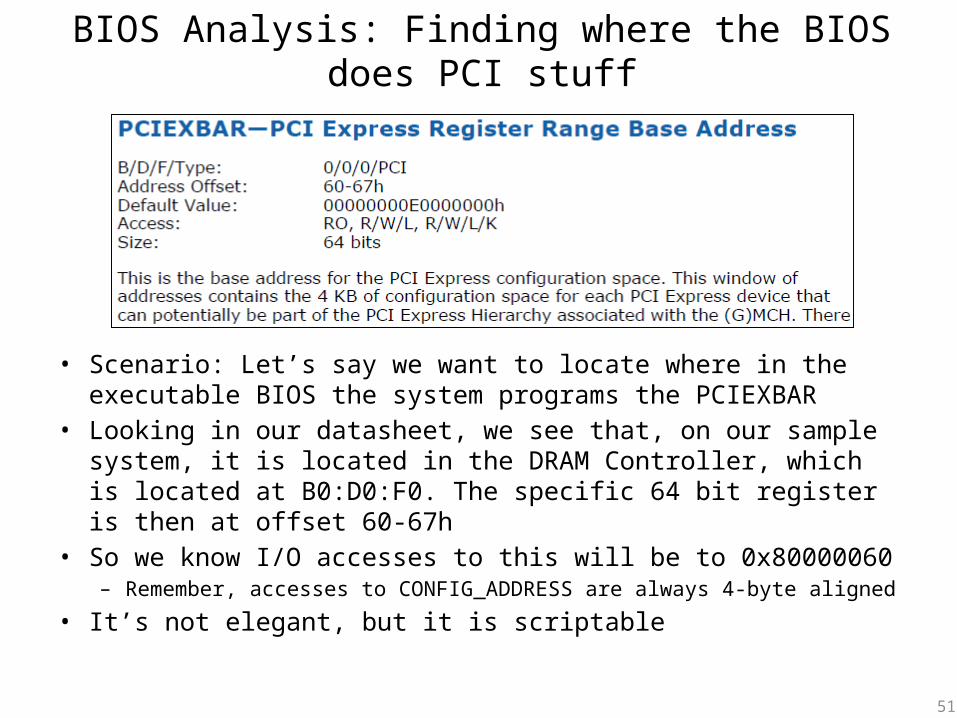
BIOS Analysis: Finding where the BIOS does PCI stuff
• Scenario: Let’s say we want to locate where in the executable BIOS the system programs the PCIEXBAR
• Looking in our datasheet, we see that, on our sample system, it is located in the DRAM Controller, which is located at B0:D0:F0. The specific 64 bit register is then at offset 60-67h
• So we know I/O accesses to this will be to 0x80000060– Remember, accesses to CONFIG_ADDRESS are always 4-byte aligned
• It’s not elegant, but it is scriptable
51
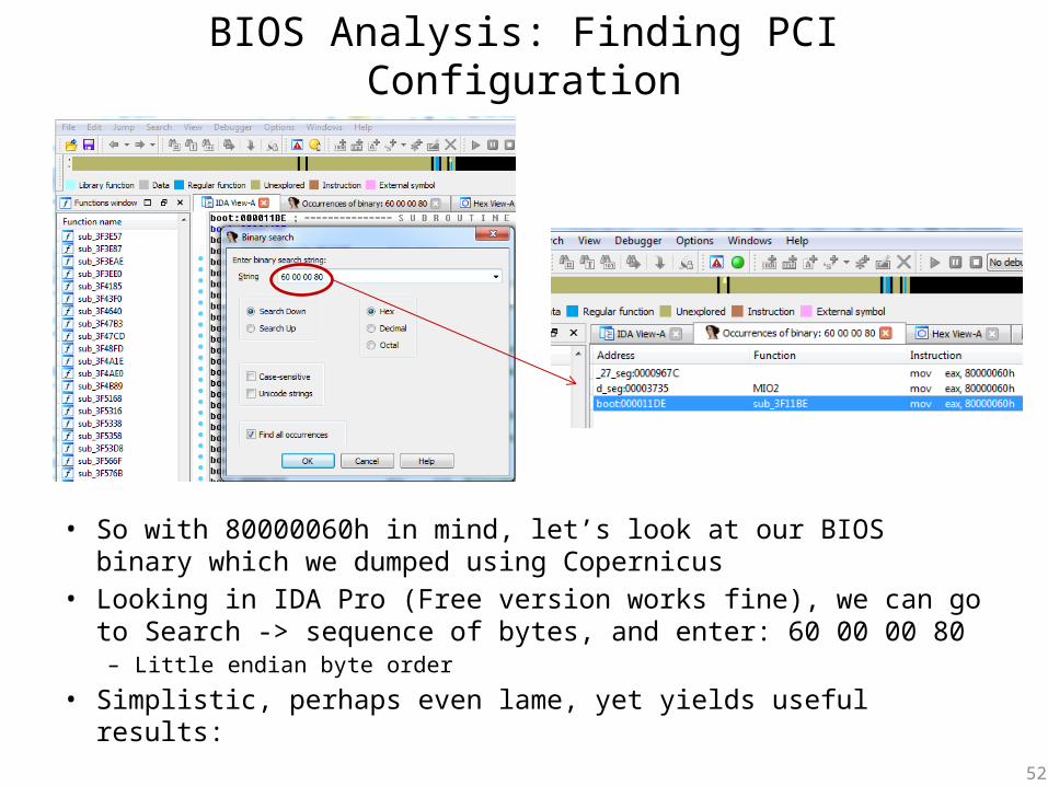
BIOS Analysis: Finding PCI Configuration
• So with 80000060h in mind, let’s look at our BIOS binary which we dumped using Copernicus
• Looking in IDA Pro (Free version works fine), we can go to Search -> sequence of bytes, and enter: 60 00 00 80– Little endian byte order
• Simplistic, perhaps even lame, yet yields useful results:52
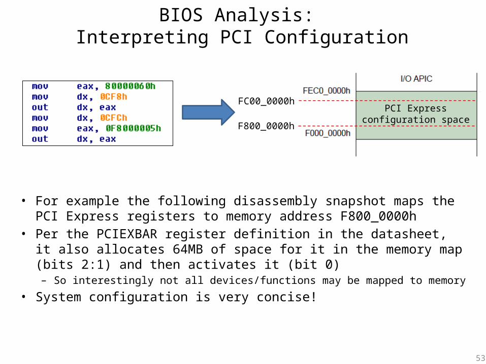
BIOS Analysis: Interpreting PCI Configuration
• For example the following disassembly snapshot maps the PCI Express registers to memory address F800_0000h
• Per the PCIEXBAR register definition in the datasheet, it also allocates 64MB of space for it in the memory map (bits 2:1) and then activates it (bit 0)– So interestingly not all devices/functions may be mapped to memory
• System configuration is very concise!
F800_0000h
FC00_0000hPCI Express
configuration space
53
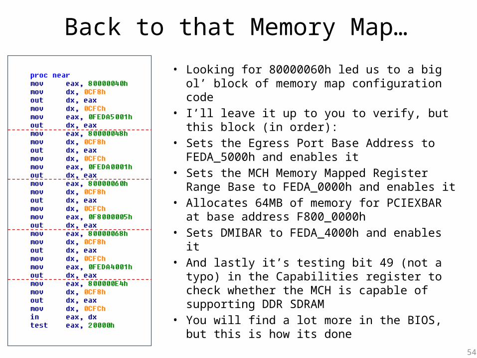
Back to that Memory Map…
• Looking for 80000060h led us to a big ol’ block of memory map configuration code
• I’ll leave it up to you to verify, but this block (in order):
• Sets the Egress Port Base Address to FEDA_5000h and enables it
• Sets the MCH Memory Mapped Register Range Base to FEDA_0000h and enables it
• Allocates 64MB of memory for PCIEXBAR at base address F800_0000h
• Sets DMIBAR to FEDA_4000h and enables it• And lastly it’s testing bit 49 (not a typo) in the
Capabilities register to check whether the MCH is capable of supporting DDR SDRAM
• You will find a lot more in the BIOS, but this is how its done
54