Advanced Universal Serial Bus Transcievers - TI.com · The device allows USB application-specific...
25
1 2 3 4 5 6 7 8 16 15 14 13 12 11 10 9 V pu(3.3) SOFTCON OE RCV VP VM SUSPND GND V CC(I/O) SPEED D - D + VPO VMO V reg(3.3) V CC(5.0) TUSB1106-Q1 www.ti.com SCAS916 – AUGUST 2011 ADVANCED UNIVERSAL SERIAL BUS TRANSCEIVERS Check for Samples: TUSB1106-Q1 1FEATURES • Available in a Thin Shrink Small-Outline Package [TSSOP (PW)] • Qualified for Automotive Applications • Compatible With Universal Serial Bus PW PACKAGE Specification Rev. 2.0 (TOP VIEW) • Transmit and Receive Serial Data at Both Full-Speed (12-Mbit/s) and Low-Speed (1.5-Mbit/s) Data Rates • Integrated Bypassable 5-V to 3.3-V Voltage Regulator for Powering Via USB V BUS • V BUS Disconnection Indication Through V P and V M • Used as USB Device Transceiver or USB Host Transceiver • Stable RCV Output During SE0 Condition • Two Single-Ended Receivers With Hysteresis • Low-Power Operation, Ideal for Portable Equipment • Support I/O Voltage Range From 1.65 V to 3.6 V DESCRIPTION The TUSB1106-Q1 universal serial bus (USB) transceiver is compliant with the Universal Serial Bus Specification Rev. 2.0. This device can transmit and receive serial data at both full-speed (12-Mbit/s) and low-speed (1.5-Mbit/s) data rates. The TUSB1106-Q1 can be used as USB device transceiver or USB host transceiver. The device allows USB application-specific ICs (ASICs) and programmable logic devices (PLDs), with power-supply voltages from 1.65 V to 3.6 V, to interface with the physical layer (PHY) of the universal serial bus. It has an integrated 5-V to 3.3-V voltage regulator for direct powering via the USB supply VBUS. The TUSB1106-Q1 allows only differential input mode and is available in a PW package. The TUSB1106-Q1 is ideal for portable electronic devices such as mobile phones, personal digital assistants, information appliances, and digital still cameras. ORDERING INFORMATION T A PACKAGE (1) (2) ORDERABLE PART NUMBER TOP-SIDE MARKING –40°C to 85°C TSSOP – PW Reel of 2000 TUSB1106IPWRQ1 TU1106I (1) Package drawings, thermal data, and symbolization are available at www.ti.com/packaging. (2) For the most current package and ordering information, see the Package Option Addendum at the end of this document, or see the TI website at www.ti.com. 1 Please be aware that an important notice concerning availability, standard warranty, and use in critical applications of Texas Instruments semiconductor products and disclaimers thereto appears at the end of this data sheet. PRODUCTION DATA information is current as of publication date. Copyright © 2011, Texas Instruments Incorporated Products conform to specifications per the terms of the Texas Instruments standard warranty. Production processing does not necessarily include testing of all parameters.
Transcript of Advanced Universal Serial Bus Transcievers - TI.com · The device allows USB application-specific...

1
2
3
4
5
6
7
8
16
15
14
13
12
11
10
9
Vpu(3 .3)
SO FTCO N
O E
R CV
VP
VM
SUSPN D
GN D V C C ( I /O )
SPEED
D −
D +
VPO
VM O
Vreg(3 .3 )
VCC (5 .0 )
TUSB1106-Q1
www.ti.com SCAS916 –AUGUST 2011
ADVANCED UNIVERSAL SERIAL BUS TRANSCEIVERSCheck for Samples: TUSB1106-Q1
1FEATURES • Available in a Thin Shrink Small-OutlinePackage [TSSOP (PW)]• Qualified for Automotive Applications
• Compatible With Universal Serial BusPW PACKAGESpecification Rev. 2.0
(TOP VIEW)• Transmit and Receive Serial Data at Both
Full-Speed (12-Mbit/s) and Low-Speed(1.5-Mbit/s) Data Rates
• Integrated Bypassable 5-V to 3.3-V VoltageRegulator for Powering Via USB VBUS
• VBUS Disconnection Indication Through VP andVM
• Used as USB Device Transceiver or USB HostTransceiver
• Stable RCV Output During SE0 Condition• Two Single-Ended Receivers With Hysteresis• Low-Power Operation, Ideal for Portable
Equipment• Support I/O Voltage Range From 1.65 V to
3.6 V
DESCRIPTIONThe TUSB1106-Q1 universal serial bus (USB) transceiver is compliant with the Universal Serial Bus SpecificationRev. 2.0. This device can transmit and receive serial data at both full-speed (12-Mbit/s) and low-speed(1.5-Mbit/s) data rates. The TUSB1106-Q1 can be used as USB device transceiver or USB host transceiver.
The device allows USB application-specific ICs (ASICs) and programmable logic devices (PLDs), withpower-supply voltages from 1.65 V to 3.6 V, to interface with the physical layer (PHY) of the universal serial bus.It has an integrated 5-V to 3.3-V voltage regulator for direct powering via the USB supply VBUS.
The TUSB1106-Q1 allows only differential input mode and is available in a PW package.
The TUSB1106-Q1 is ideal for portable electronic devices such as mobile phones, personal digital assistants,information appliances, and digital still cameras.
ORDERING INFORMATIONTA PACKAGE (1) (2) ORDERABLE PART NUMBER TOP-SIDE MARKING
–40°C to 85°C TSSOP – PW Reel of 2000 TUSB1106IPWRQ1 TU1106I
(1) Package drawings, thermal data, and symbolization are available at www.ti.com/packaging.(2) For the most current package and ordering information, see the Package Option Addendum at the end of this document, or see the TI
website at www.ti.com.
1
Please be aware that an important notice concerning availability, standard warranty, and use in critical applications of TexasInstruments semiconductor products and disclaimers thereto appears at the end of this data sheet.
PRODUCTION DATA information is current as of publication date. Copyright © 2011, Texas Instruments IncorporatedProducts conform to specifications per the terms of the TexasInstruments standard warranty. Production processing does notnecessarily include testing of all parameters.
TUSB1106-Q1
TUSB1106-Q1
SCAS916 –AUGUST 2011 www.ti.com
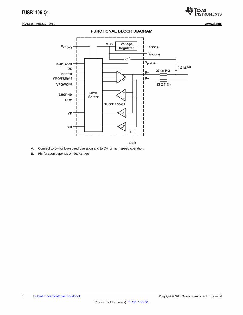
FUNCTIONAL BLOCK DIAGRAM
A. Connect to D– for low-speed operation and to D+ for high-speed operation.
B. Pin function depends on device type.
2 Submit Documentation Feedback Copyright © 2011, Texas Instruments Incorporated
Product Folder Link(s): TUSB1106-Q1

TUSB1106-Q1
www.ti.com SCAS916 –AUGUST 2011
TERMINAL FUNCTIONSTERMINAL
I/O DESCRIPTIONNAME NO.
Output enable (CMOS level with respect to VCC(I/O), active LOW). Enables the transceiver toOE 3 I transmit data on the USB bus input pad. Push pull, CMOS.
Differential data receiver (CMOS level with respect to VCC(I/O)). Driven LOW when inputRCV 4 O SUSPND is HIGH. The output state of RCV is preserved and stable during an SE0 condition
output pad. Push pull, 4-mA output drive, CMOS.
Single-ended D+ receiver (CMOS level with respect to V). For external detection of single-endedVP 5 O zero (SE0), error conditions, speed of connected device. Driven HIGH when no supply voltage
is connected to VCC(5.0) and Vreg(3.3) output pad. Push pull, 4-mA output drive, CMOS.
Single-ended D– receiver (CMOS level with respect to VCC(I/O)). For external detection ofsingle-ended zero (SE0), error conditions, speed of connected device. Driven HIGH when noVM 6 O supply voltage is connected to VCC(5.0) and Vreg(3.3) output pad. Push pull, 4-mA output drive,CMOS.
Suspend (CMOS level with respect to VCC(I/O)). A HIGH level enables low-power state while theSUSPND 7 I USB bus is inactive and drives output RCV to a LOW-level input pad. Push pull, CMOS.
Mode (CMOS level with respect to VCC(I/O)). A HIGH level enables the differential input modeMODE I (VPO, VMO), whereas a LOW level enables a single-ended input mode (VO, FSE0). See Table
5 and Table 6 input pad. Push pull, CMOS.
GND 8 Ground supply
Supply voltage for digital I/O pins (1.65 to 3.6 V). When VCC(I/O) is not connected, the D+ andVCC(I/O) 9 D– pins are in 3-state. This supply pin is independent of VCC(5.0) and Vreg(3.3) and must never
exceed the Vreg(3.3) voltage.
Speed selection (CMOS level with respect to VCC(I/O)). Adjusts the slew rate of differential dataoutputs D+ and D– according to the transmission speed. Input pad, push pull, CMOS.SPEED 10 I LOW – low speed (1.5 Mbit/s)HIGH – full speed (12 Mbit/s)
Negative USB data bus connection (analog, differential). For low-speed mode, connect to pinD– 11 AI/O Vpu(3.3) via a 1.5-kΩ resistor.
Positive USB data bus connection (analog, differential). For full-speed mode, connect to pinD+ 12 AI/O Vpu(3.3) via a 1.5-kΩ resistor.
VPO/VO I Driver data (CMOS level with respect to VCC(I/O), Schmitt trigger). See Driving Function table.Push pull, CMOS.VPO 13
VMO/FSE0 I Driver data (CMOS level with respect to VCC(I/O), Schmitt trigger). See Driving Function table.Push pull, CMOS.VMO 14
Internal regulator option. Regulated supply-voltage output (3 V to 3.6 V) during 5-V operation. Adecoupling capacitor of at least 0.1 mF is required for the regulator bypass option. Used as aVreg(3.3) 15 supply-voltage input for3.3 V ± 10% operation.
Internal regulator option. Supply-voltage input (4 V to 5.5 V). Can be connected directly to USBVCC(5.0) 16 supply VBUS regulator bypass option. Connect to Vreg(3.3).
Pullup supply voltage (3.3 V ± 10%). Connect an external 1.5-kΩ resistor on D+ (full speed) orD– (low speed). Pin function is controlled by input SOFTCON.Vpu(3.3) 1 SOFTCON = LOW – Vpu(3.3) floating (high impedance), ensures zero pullup currentSOFTCON = HIGH – Vpu(3.3) = 3.3 V, internally connected to Vreg(3.3)
Software-controlled USB connection. A HIGH level applies 3.3 V to pin Vpu(3.3), which isSOFTCON 2 I connected to an external 1.5-kΩ pullup resistor. This allows USB connect/disconnect signaling
to be controlled by software input pad. Push pull, CMOS.
Copyright © 2011, Texas Instruments Incorporated Submit Documentation Feedback 3
Product Folder Link(s): TUSB1106-Q1
TUSB1106-Q1
SCAS916 –AUGUST 2011 www.ti.com
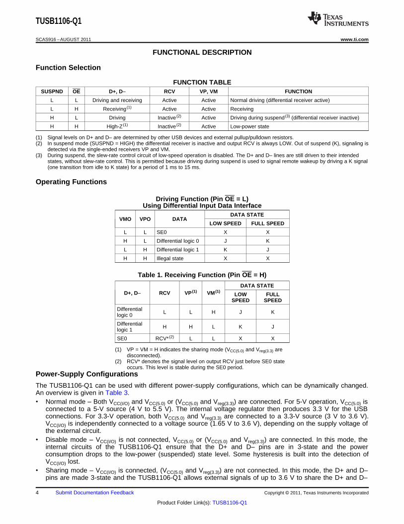
FUNCTIONAL DESCRIPTION
Function Selection
FUNCTION TABLESUSPND OE D+, D– RCV VP, VM FUNCTION
L L Driving and receiving Active Active Normal driving (differential receiver active)
L H Receiving (1) Active Active Receiving
H L Driving Inactive (2) Active Driving during suspend (3) (differential receiver inactive)
H H High-Z (1) Inactive (2) Active Low-power state
(1) Signal levels on D+ and D– are determined by other USB devices and external pullup/pulldown resistors.(2) In suspend mode (SUSPND = HIGH) the differential receiver is inactive and output RCV is always LOW. Out of suspend (K), signaling is
detected via the single-ended receivers VP and VM.(3) During suspend, the slew-rate control circuit of low-speed operation is disabled. The D+ and D– lines are still driven to their intended
states, without slew-rate control. This is permitted because driving during suspend is used to signal remote wakeup by driving a K signal(one transition from idle to K state) for a period of 1 ms to 15 ms.
Operating Functions
Driving Function (Pin OE = L)Using Differential Input Data Interface
DATA STATEVMO VPO DATA
LOW SPEED FULL SPEED
L L SE0 X X
H L Differential logic 0 J K
L H Differential logic 1 K J
H H Illegal state X X
Table 1. Receiving Function (Pin OE = H)
DATA STATED+, D– RCV VP (1) VM (1)
LOW FULLSPEED SPEED
Differential L L H J Klogic 0
Differential H H L K Jlogic 1
SE0 RCV* (2) L L X X
(1) VP = VM = H indicates the sharing mode (VCC(5.0) and Vreg(3.3) aredisconnected).
(2) RCV* denotes the signal level on output RCV just before SE0 stateoccurs. This level is stable during the SE0 period.
Power-Supply Configurations
The TUSB1106-Q1 can be used with different power-supply configurations, which can be dynamically changed.An overview is given in Table 3.• Normal mode – Both VCC(I/O) and VCC(5.0) or (VCC(5.0) and Vreg(3.3)) are connected. For 5-V operation, VCC(5.0) is
connected to a 5-V source (4 V to 5.5 V). The internal voltage regulator then produces 3.3 V for the USBconnections. For 3.3-V operation, both VCC(5.0) and Vreg(3.3) are connected to a 3.3-V source (3 V to 3.6 V).VCC(I/O) is independently connected to a voltage source (1.65 V to 3.6 V), depending on the supply voltage ofthe external circuit.
• Disable mode – VCC(I/O) is not connected, VCC(5.0) or (VCC(5.0) and Vreg(3.3)) are connected. In this mode, theinternal circuits of the TUSB1106-Q1 ensure that the D+ and D– pins are in 3-state and the powerconsumption drops to the low-power (suspended) state level. Some hysteresis is built into the detection ofVCC(I/O) lost.
• Sharing mode – VCC(I/O) is connected, (VCC(5.0) and Vreg(3.3)) are not connected. In this mode, the D+ and D–pins are made 3-state and the TUSB1106-Q1 allows external signals of up to 3.6 V to share the D+ and D–
4 Submit Documentation Feedback Copyright © 2011, Texas Instruments Incorporated
Product Folder Link(s): TUSB1106-Q1

TUSB1106-Q1
www.ti.com SCAS916 –AUGUST 2011
lines. The internal circuits of the TUSB1106-Q1 ensure that virtually no current (maximum 10 μA) is drawn viathe D+ and D– lines. The power consumption through VCC(I/O) drops to the low-power (suspended) state level.Both the VP and VM pins are driven HIGH to indicate this mode. Pin RCV is made LOW. Some hysteresis isbuilt into the detection of Vreg(3.3) lost.
Table 2. Pin States in Disable or Sharing Mode
PINS DISABLE-MODE STATE SHARING-MODE STATE
VCC(5.0)/Vreg(3.3) 5-V input/3.3-V output, 3.3-V input/3.3-V input Not present
VCC(I/O) Not present 1.65-V to 3.6-V input
Vpu(3.3) High impedance (off) High impedance (off)
D+, D– High impedance High impedance
VP, VM Invalid (1) H
RCV Invalid (2) L
Inputs (VO/VPO, FSE0/VMO, SPEED, High impedance High impedanceSUSPND, OE, SOFTCON)
(1) High impedance or driven LOW(2) High impedance or driven LOW
Table 3. Power-Supply Configuration Overview
VCC(5.0) or Vreg(3.3) VCC(I/O) CONFIGURATION SPECIAL CHARACTERISTICS
Connected Connected Normal mode
D+, D–, and Vpu(3.3) are in high impedance.Connected Not connected Disable mode VP, VM, and RCV are invalid. (1)
D+, D–, and Vpu(3.3) are in high impedance.Not connected Connected Sharing mode VP and VM are driven HIGH. RCV is driven LOW.
(1) High impedance or driven LOWPower-Supply Input Options
The TUSB1106-Q1 has two power-supply input options.• Internal regulator – VCC(5.0) is connected to 4 V to 5.5 V. The internal regulator is used to supply the internal
circuitry with 3.3 V (nominal). Vreg(3.3) becomes a 3.3-V output reference.• Regulator bypass – VCC(5.0) and Vreg(3.3) are connected to the same supply. The internal regulator is bypassed
and the internal circuitry is supplied directly from the Vreg(3.3) power supply. The voltage range is3 V to 3.6 V to comply with the USB specification.
The supply-voltage range for each input option is specified in Table 4.
Table 4. Power-Supply Input Options
INPUT OPTION VCC(5.0) VREG(3.3) VCC(I/O)
Supply input for internal regulator Voltage-reference output Supply input for digital I/O pinsInternal regulator (4 V to 5.5 V) (3.3 V, 300 μA) (1.65 V to 3.6 V)
Connected to Vreg(3.3) with Supply input Supply input for digital I/O pinsRegulator bypass maximum voltage drop of 0.3 V (3 V to 3.6 V) (1.65 V to 3.6 V)(2.7 V to 3.6 V)
Copyright © 2011, Texas Instruments Incorporated Submit Documentation Feedback 5
Product Folder Link(s): TUSB1106-Q1

TUSB1106-Q1
SCAS916 –AUGUST 2011 www.ti.com
ABSOLUTE MAXIMUM RATINGS (1)
over operating free-air temperature range (unless otherwise noted)
MIN MAX UNIT
VCC(5.0) Supply voltage range –0.5 6 V
VI(I/O) Supply voltage range –0.5 4.6 V
VCCreg(3.3) Regulated voltage range –0.5 4.6 V
VI DC input voltage –0.5 VCC(I/O) + 0.5 V
IIK Input clamp current VI = –1.8 V to 5.4 V 100 mA
Tstg Storage temperature range –40 125 °C
(1) Stresses beyond those listed under "absolute maximum ratings" may cause permanent damage to the device. These are stress ratingsonly, and functional operation of the device at these or any other conditions beyond those indicated under "recommended operatingconditions" is not implied. Exposure to absolute-maximum-rated conditions for extended periods may affect device reliability.
RECOMMENDED OPERATING CONDITIONSMIN NOM MAX UNIT
VCC(5.0) Supply voltage, internal regulator option 5-V operation 4 5 5.5 V
VCCreg(3.3) Supply voltage, regulator bypass option 3.3-V operation 3 3.3 3.6 V
VCC(I/O) I/O supply voltage 1.65 3.6 V
VI I/O supply voltage 0 VCC(I/O) V
VI/O Input voltage on analog I/O pins (D+, D–) 0 3.6 V
Tc Junction temperature –40 85 °C
6 Submit Documentation Feedback Copyright © 2011, Texas Instruments Incorporated
Product Folder Link(s): TUSB1106-Q1

TUSB1106-Q1
www.ti.com SCAS916 –AUGUST 2011
STATIC ELECTRICAL CHARACTERISTICS – SUPPLY PINSover recommended ranges of operating free-air temperature and supply voltage (unless otherwise noted)
PARAMETER TEST CONDITIONS MIN TYP MAX UNIT
RegulatedVreg(3.3) Internal regulator option, Iload ≤ 300 μA (1) (2) 3 3.3 3.6 Vsupply-voltage output
Full-speed transmitting and receiving at 12 Mbit/s,ICC Operating supply current 6 8 mACL = 50 pF on D+ and D– (3)
ICC(I/O) Operating I/O supply current Full-speed transmitting and receiving at 12 Mbit/s (3) 2.3 2.5 mA
Full-speed idle:Supply current during VD+ > 2.7 V, VD– < 0.3 VICC(idle) 500 μAfull-speed idle and SE0 SE0:
VD+ < 0.3 V, VD– < 0.3 V (4)
ICC(I/O)(static) Static I/O supply current Full-speed idle, SE0 or suspend 10 22 μA
ICC(susp) Suspend supply current SUSPND = HIGH (4) 10 22 μA
ICC(dis) Disable-mode supply current VCC(I/O) not connected (4) 10 22 μA
Sharing-mode I/OICC(I/O)(sharing) VCC(5.0) or Vreg(3.3) not connected 10 22 μAsupply current
Sharing-mode load current VCC(5.0) or Vreg(3.3) not connected,IDx(sharing) 10 μAon D+ and D– SOFTCON = LOW, VDx = 3.6 V
Supply lost 0.8during power downRegulated supply-voltage 1.65 V ≤ VCC(I/O) ≤ Vreg(3.3),Vreg(3.3)th Vdetection threshold 2.7 V ≤ Vreg(3.3) ≤ 3.6 V Supply detect 2.4during power up (5)
Regulated supply-voltageVreg(3.3)hys VCC(I/O) = 1.8 V 0.45 Vdetection hysteresis
Supply lost 0.5during power downI/O supply-voltageVCC(I/O)th Vreg(3.3) = 2.7 V to 3.6 V Vdetection threshold Supply detect 1.4during power up
I/O supply-voltageVCC(I/O)hys Vreg(3.3) = 3.3 V 0.45 Vdetection hysteresis
(1) Iload includes the pullup resistor current via Vpu(3.3).(2) In suspend mode, the typical voltage is 2.8 V.(3) Maximum value is characterized only, not tested in production.(4) Excluding any load current and Vpu(3.3)/Vsw source current to the 1.5-kΩ and 15-kΩ pullup and pulldown resistors (200 μA typ)(5) When VCC(I/O) < 2.7 V, the minimum value for Vreg(3.3)th (present) is 2 V.
Copyright © 2011, Texas Instruments Incorporated Submit Documentation Feedback 7
Product Folder Link(s): TUSB1106-Q1

TUSB1106-Q1
SCAS916 –AUGUST 2011 www.ti.com
STATIC ELECTRICAL CHARACTERISTICS – DIGITAL PINSover recommended ranges of operating free-air temperature and supply voltage (unless otherwise noted)
PARAMETER TEST CONDITIONS VCC(I/O) MIN MAX UNIT
VIL LOW-level input voltage 1.65 V to 3.6 V 0.3 VCC(I/O) V
VIH HIGH-level input voltage 1.65 V to 3.6 V 0.6 VCC(I/O) V
IOL = 100 μA 0.151.65 V to 3.6 V
IOL = 2 mA 0.4
IOL = 100 μA 0.151.8 V ± 0.15 V
IOL = 2 mA 0.4VOL LOW-level output voltage V
IOL = 100 μA 0.152.5 V ± 0.2 V
IOL = 2 mA 0.4
IOL = 100 μA 0.153.3 V ± 0.3 V
IOL = 2 mA 0.4
IOH = 100 μA VCC(I/O) – 0.151.65 V to 3.6 V
IOH = 2 mA VCC(I/O) – 0.4
IOH = 100 μA 1.51.8 V ± 0.15 V
IOH = 2 mA 1.25VOH HIGH-level output voltage V
IOH = 100 μA 2.152.5 V ± 0.2 V
IOH = 2 mA 1.9
IOH = 100 μA 2.853.3 V ± 0.3 V
IOH = 2 mA 2.6
ILI Input leakage current –1 1 μA
CIN Input capacitance Pin to GND 3.5 pF
8 Submit Documentation Feedback Copyright © 2011, Texas Instruments Incorporated
Product Folder Link(s): TUSB1106-Q1

TUSB1106-Q1
www.ti.com SCAS916 –AUGUST 2011
STATIC ELECTRICAL CHARACTERISTICS – ANALOG I/O PINSover recommended ranges of operating free-air temperature and supply voltage, VCC = 4 V to 5.5 V or Vreg(3.3) = 3 V to 3.6 V,VGND = 0 V, TA = –40°C to 85°C (unless otherwise noted)
PARAMETER TEST CONDITIONS MIN TYP MAX UNIT
VDI Differential input sensitivity |VI(D+) – VI(D–)| 0.2 V
VCM Differential common-mode voltage Includes VDI range 0.8 2.5 V
VIL LOW-level input voltage, single-ended receiver 2 0.8 V
VIH HIGH-level input voltage, single-ended receiver 0.4 V
Vhys Hysteresis voltage, single-ended receiver 0.7 V
VOL LOW-level output voltage RL = 1.5 kΩ to 3.6 V 0.3 V
VOH HIGH-level output voltage RL = 1.5 kΩ to GND 2.8 (1) 3.6 V
ILZ OFF-state leakage current 1 μA
CIN Transceiver capacitance Pin to GND 25 pF
ZDRV Driver output impedance Steady-state drive 34 (2) 39 44 ΩZINP Input impedance 10 MΩRSW Internal switch resistance at Vpu(3.3) 13 ΩVTERM Termination voltage for upstream port pullup (RPU) 3 (3) (4) 3.6 V
(1) VOH(min) = Vreg(3.3) – 0.2 V(2) Includes external resistors of 33 Ω ±1% on both D+ and D–(3) This voltage is available at Vreg(3.3) and Vpu(3.3).(4) In suspend mode, the minimum voltage is 2.7 V.
Copyright © 2011, Texas Instruments Incorporated Submit Documentation Feedback 9
Product Folder Link(s): TUSB1106-Q1

TUSB1106-Q1
SCAS916 –AUGUST 2011 www.ti.com
DYNAMIC ELECTRICAL CHARACTERISTICS – ANALOG I/O PINS (D+, D–) (1) (2)
Driver Characteristics, Full-Speed Modeover recommended ranges of operating free-air temperature and supply voltage, VCC = 4 V to 5.5 V or Vreg(3.3) = 3 V to 3.6 V,VCC(I/O) = 1.65 V to 3.6 V, VGND = 0 V, see Table 10 for valid voltage level combinations, TA = –40°C to 85°C(unless otherwise noted)
PARAMETER TEST CONDITIONS MIN MAX UNIT
CL = 50 pF to 125 pF,tFR Rise time 4 20 ns10% to 90% of |VOH – VOL| (see Figure 1)
CL = 50 pF to 125 pF,tFF Fall time 4 20 ns90% to 10% of |VOH – VOL| (see Figure 1)
Differential rise/fall time matchingFRFM Excluding the first transition from idle state 90 111.1 %(tFR/tFF)
VCRS Output signal crossover voltage Excluding the first transition from idle state (see Figure 10) 1.3 2 V
(1) Test circuit, see Figure 13(2) Driver timing in low-speed mode is not specified. Low-speed delay timings are dominated by the slow rise/fall times tLR and tLF.
DYNAMIC ELECTRICAL CHARACTERISTICS – ANALOG I/O PINS (D+, D–) (1) (2)
Driver Characteristics, Low-Speed Modeover recommended ranges of operating free-air temperature and supply voltage, VCC = 4 V to 5.5 V or Vreg(3.3) = 3 V to 3.6 V,VCC(I/O) = 1.65 V to 3.6 V, VGND = 0 V, see Table 10 for valid voltage level combinations, TA = –40°C to 85°C(unless otherwise noted)
PARAMETER TEST CONDITIONS MIN MAX UNIT
CL = 200 pF to 600 pF,tLR Rise time 75 300 ns10% to 90% of |VOH – VOL| (see Figure 1)
CL = 200 pF to 600 pF,tLF Fall time 75 300 ns90% to 10% of |VOH – VOL| (see Figure 1)
Differential rise/fall time matchingLRFM Excluding the first transition from idle state 80 125 %(tLR/tLF)
VCRS Output signal crossover voltage Excluding the first transition from idle state (see Figure 10) 1.3 2 V
(1) Test circuit, see Figure 13(2) Driver timing in low-speed mode is not specified. Low-speed delay timings are dominated by the slow rise/fall times tLR and tLF.
DYNAMIC ELECTRICAL CHARACTERISTICS – ANALOG I/O PINS (D+, D–) (1) (2)
Driver Timing, Full-Speed Modeover recommended ranges of operating free-air temperature and supply voltage, VCC = 4 V to 5.5 V or Vreg(3.3) = 3 V to 3.6 V,VCC(I/O) = 1.65 V to 3.6 V, VGND = 0 V, see Table 10 for valid voltage level combinations, TA = –40°C to 85°C(unless otherwise noted)
PARAMETER TEST CONDITIONS MIN MAX UNIT
tPLH(drv) LOW to HIGH (see Figure 4) 18Driver propagation delay ns(VO/VPO, FSE0/VMO to D+, D–)tPHL(drv) HIGH to LOW (see Figure 4) 18
tPHZ HIGH to OFF (see Figure 2) 15Driver disable delay (OE to D+, D–) ns
tPLZ LOW to OFF (see Figure 2) 15
tPZH OFF to HIGH (see Figure 2) 15Driver enable delay (OE to D+, D–) ns
tPZL OFF to LOW (see Figure 2) 15
(1) Test circuit, see Figure ?(2) Driver timing in low-speed mode is not specified. Low-speed delay timings are dominated by the slow rise/fall times tLR and tLF.
10 Submit Documentation Feedback Copyright © 2011, Texas Instruments Incorporated
Product Folder Link(s): TUSB1106-Q1

MGS963
10%
90% 90%
10%VOL
VOH
tFR,tLR tFF,tLF
MGS966
Logic Input
DifferentialData Lines
1.8 V
0 V
VOH
VOL
0.9 V 0.9 V
VOL + 0.3 V
VOH − 0.3 VVCRS
tPZHtPZL
tPHZtPLZ
MGS964VOL
Logic Output
VOH
DifferentialData Lines
0.9 V
VCRS VCRS
1.8 V
0 VtPLH(drv) tPHL(drv)
0.9 V
MGS965VOL
Logic Output
VOH
0.8 V
DifferentialData Lines
2.0 V
VCRS
0.9 V 0.9 V
VCRS
tPLH(rcv)tPLH(se)
tPHL(rcv)tPHL(se)
TUSB1106-Q1
www.ti.com SCAS916 –AUGUST 2011
DYNAMIC ELECTRICAL CHARACTERISTICS FOR ANALOG I/O PINS (D+, D–) (1)
Receiver Timing, Full-Speed and Low-Speed Mode, Differential Receiverover recommended ranges of operating free-air temperature and supply voltage, VCC = 4 V to 5.5 V or Vreg(3.3) = 3 V to 3.6 V,VCC(I/O) = 1.65 V to 3.6 V, VGND = 0 V, see Table 10 for valid voltage level combinations, TA = –40°C to 85°C(unless otherwise noted)
PARAMETER TEST CONDITIONS MIN MAX UNIT
tPLH(rcv) LOW to HIGH (see Figure 3) 15Propagation delay (D+, D– to RCV) ns
tPHL(rcv) HIGH to LOW (see Figure 3) 15
(1) Test circuit, see Figure ?
DYNAMIC ELECTRICAL CHARACTERISTICS FOR ANALOG I/O PINS (D+, D–) (1)
Receiver Timing, Full-Speed and Low-Speed Mode, Single-Ended Receiverover recommended ranges of operating free-air temperature and supply voltage, VCC = 4 V to 5.5 V or Vreg(3.3) = 3 V to 3.6 V,VCC(I/O) = 1.65 V to 3.6 V, VGND = 0 V, see Table 10 for valid voltage level combinations, TA = –40°C to 85°C(unless otherwise noted)
PARAMETER TEST CONDITIONS MIN MAX UNIT
tPLH(se) LOW to HIGH (see Figure 3) 18Propagation delay (D+, D– to VP, VM) ns
tPHL(se) HIGH to LOW (see Figure 3) 18
(1) Test circuit, see Figure 13
Figure 1. Rise and Fall Times Figure 2. OE to D+, D–
Figure 3. D+, D– to RCV, VP, VM Figure 4. VO/VPO, FSE0/VMO to D+, D–
Copyright © 2011, Texas Instruments Incorporated Submit Documentation Feedback 11
Product Folder Link(s): TUSB1106-Q1

Test Point
D.U.T.
V
+
–
33 Ω 500 Ω
50 pF
MBL142
Test Point
D.U.T.
MGS968
25 pF
Test Point
D.U.T.
D+/D–
1.5 kΩ
15 kΩ
33 Ω
VPU(3.3)
CL
TUSB1106-Q1
SCAS916 –AUGUST 2011 www.ti.com
APPLICATION INFORMATION
Figure 5. Load for Enable and Disable Times
A. V = 0 V for tPZH, tPHZ
B. V = Vreg(3.3) for tPZL, tPLZ
Figure 6. Load for VM, VP, and RCV
Figure 7. Load for D+, D–A. Full-speed mode: connected to D+
B. Low-speed mode: Connected to D–C. Load capacitance:
• CL = 50 pF or 125 pF (full-speed mode, minimum or maximum timing)
• CL = 200 pF or 600 pF (low-speed mode, minimum or maximum timing)
12 Submit Documentation Feedback Copyright © 2011, Texas Instruments Incorporated
Product Folder Link(s): TUSB1106-Q1

Vpu(3.3)
SPEED
SOFTCON
RCV
VPO/VO
VP
VM
1.65 V to 3.6 V
System ASIC
D–
D+
1.5 kW
VBUS
VCC(5.0)
OE
Vreg(3.3)
SUSPND
VMO/FSE0
VCC(I/O)
0.1 µF
3.3 V
VCC
33 W
33 W
0.1 µF
0.1 µF
TUSB1106-Q1
GND
GND
GND
GND
GND
TUSB1106-Q1
www.ti.com SCAS916 –AUGUST 2011
Figure 8. Peripheral-Side (Full-Speed) Regulator Bypass Mode
Peripheral-Side (Full-Speed) Regulator Bypass Mode
This mode is applicable when there is a 3.3-V supply already available on the board. The VBUS pin of the USBconnector, if left unused at the peripheral side, should be terminated with a 0.1-μF capacitor. While operating atfull speed, the 1.5-kΩ resistor must be connected between the D+ line and VPU(3.3) or an external 3.3-V supply.When the VCC(5.0) and the Vreg(3.3) are connected together, the device operates at regulator bypass mode. Thisenables power savings since the regulator is turned off.
Copyright © 2011, Texas Instruments Incorporated Submit Documentation Feedback 13
Product Folder Link(s): TUSB1106-Q1

Vpu(3.3)
SPEED
SOFTCON
RCV
VPO/VO
VP
VM
1.65 V to 3.6 V
System ASIC
D–
D+
1.5 kW VBUS
VCC(5.0)
OE
Vreg(3.3)
SUSPND
VMO/FSE0
VCC(I/O)
0.1 µF
3.3 V
VCC
33 W
33 W
0.1 µF
0.1 µF
TUSB1106-Q1
GND
GND
GND
GND
GND
TUSB1106-Q1
SCAS916 –AUGUST 2011 www.ti.com
Figure 9. Peripheral-Side (Low-Speed) Regulator Bypass Mode
Peripheral-Side (Low-Speed) Regulator Bypass Mode
This mode is applicable when there is a 3.3-V supply already available on the board. The VBUS pin of the USBconnector, if left unused at the peripheral side, should be terminated with a 0.1-μF capacitor. While operating atlow speed, the 1.5-kΩ resistor must to be connected between the D– line and VPU(3.3) or an external 3.3-Vsupply. When the VCC(5.0) and the Vreg(3.3) are connected together, the device operates at regulator bypass mode.This enables power savings since the regulator is turned off.
14 Submit Documentation Feedback Copyright © 2011, Texas Instruments Incorporated
Product Folder Link(s): TUSB1106-Q1

V(3.3)PU
SPEED
SOFTCON
RCV
VPO/VO
VP
VM
1.65 V to 3.6 V
System ASIC
D–
D+
1.5 kW
VBUS
VCC(5.0)
OE
Vreg(3.3)
SUSPND
VMO/FSE0
VCC(I/O)
0.1 µF
0.1 µF
0.1 µF
VCC
33 W
33 W
TUSB1106-Q1
GND
GND
GND
GND
GND
TUSB1106-Q1
www.ti.com SCAS916 –AUGUST 2011
Figure 10. Peripheral-Side (Full-Speed) Internal Regulator Mode
Peripheral-Side (Full-Speed) Internal Regulator Mode
The USB side of the TUSB1106-Q1 can be powered from the VBUS line directly if a 3.3-V supply is not present onboard. In this case, the internal regulator can be used to provide the 3.3-V supply for USB signaling. The VCC(5.0)is connected to the VBUS, which receives 5-V supply from the host, and generates the 3.3-V output at the Vreg(3.3)pin. In this mode, it is important that both VCC(5.0) and Vreg(3.3) pins have individual bypass capacitors in the rangeof 0.1 μF. Powering VCC(5.0) through the VBUS port of the USB connector realizes significant power saving forportable applications, such as cell phones, PDAs, etc. In this operating mode, the ICC(5.0) current is fed from thehost. The USB-side power consumption, ICC(5.0) is 4 mA (with the regulator active), as opposed to logic-sideICC(IO) of 1 mA under full-speed operation. While operating at full speed, the 1.5-kΩ resistor must be connectedbetween the D+ line and the VPU(3.3) or an external 3.3-V supply.
Copyright © 2011, Texas Instruments Incorporated Submit Documentation Feedback 15
Product Folder Link(s): TUSB1106-Q1

V(3.3)PU
SPEED
SOFTCON
RCV
VPO/VO
VP
VM
1.65 V to 3.6 V
System ASIC
D–
D+
1.5 kWV
BUS
VCC(5.0)
OEV
reg(3.3)
SUSPND
VMO/FSE0
VCC(I/O)
0.1 µF
0.1 µF
0.1 µF
VCC
33 W
33 W
TUSB1106-Q1
GND
GND
GND
GND
GND
TUSB1106-Q1
SCAS916 –AUGUST 2011 www.ti.com
Figure 11. Peripheral-Side (Low-Speed) Internal Regulator Mode
Peripheral-Side (Low-Speed) Internal Regulator Mode
The USB side of the TUSB1106-Q1 can be powered from the VBUS line directly if a 3.3-V supply is not present onboard. In this case, the internal regulator can be used to provide the 3.3-V supply for the USB signaling. TheVCC(5.0) is connected to the VBUS, which receives 5-V supply from the host, and generates the 3.3-V output at theVreg(3.3) pin. In this mode, it is important that both VCC(5.0) and Vreg(3.3) pins have individual bypass capacitors inthe range of 0.1 μF. Powering VCC(5.0) through the VBUS port of the USB connector realizes significant powersaving for portable applications, such as cell phones, PDAs, etc. In this operating mode, the ICC(5.0) current is fedfrom the host side. The USB-side power consumption, ICC(5.0) is 4 mA (with the regulator active), as opposed tologic-side ICC(IO) of 1 mA under full-speed operation. While operating at low speed, the 1.5-kΩ resistor must beconnected between the D– line and the VPU(3.3) or an external 3.3-V supply.
16 Submit Documentation Feedback Copyright © 2011, Texas Instruments Incorporated
Product Folder Link(s): TUSB1106-Q1

Vpu(3.3)
VCC(5.0)
Vreg(3.3)
1.65 V to 3.6 V
System ASIC
15 kW
VBUS
5 V 5 V
D–
D+
SPEED
SOFTCON
RCV
VPO/VO
VP
VM
OE
SUSPND
VMO/FSE0
VCC(I/O)
0.1 µF
VCC
33 W
33 W
0.1 µF
0.1 µF
15 kW
TUSB1106-Q1
GND
GND
GND
GNDGND
GND
GND
TUSB1106-Q1
www.ti.com SCAS916 –AUGUST 2011
Figure 12. Host Side (VCC(5.0) Supplied From VBUS Pin)
Host Side (VCC(5.0) Supplied From VBUS Pin)
If there is no 3.3-V supply on board, an external 5-V supply can support the USB-side power needs. When theVCC(5.0) is connected to an external 5-V supply, the on-chip regulator generates the 3.3-V internal supply rail,which is used to drive the USB signaling levels at the USB side of the TUSB1106-Q1. The logic-side I/Os canoperate at any voltage range from 1.65 V to 3.6 V.
Copyright © 2011, Texas Instruments Incorporated Submit Documentation Feedback 17
Product Folder Link(s): TUSB1106-Q1
Vpu(3.3)
VCC(5.0)
Vreg(3.3)
1.65 V to 3.6 V
System ASIC
15 kW
VBUS
D–
D+
SPEED
SOFTCON
RCV
VPO/VO
VP
VM
OE
SUSPND
VMO/FSE0
VCC(I/O)
0.1 µF
VCC
33 W
33 W
0.1 µF
15 kW
3.3 V
5 V
TUSB1106-Q1
GND
GND
GND GND GND
GND
TUSB1106-Q1
SCAS916 –AUGUST 2011 www.ti.com
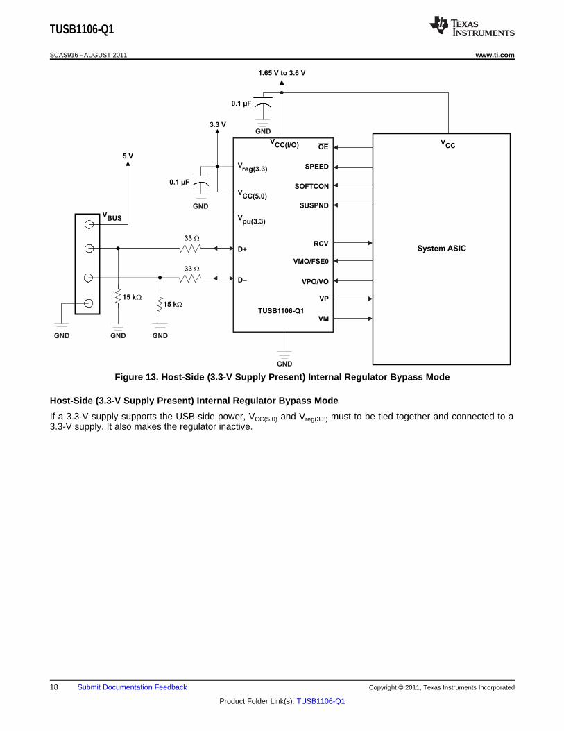
Figure 13. Host-Side (3.3-V Supply Present) Internal Regulator Bypass Mode
Host-Side (3.3-V Supply Present) Internal Regulator Bypass Mode
If a 3.3-V supply supports the USB-side power, VCC(5.0) and Vreg(3.3) must to be tied together and connected to a3.3-V supply. It also makes the regulator inactive.
18 Submit Documentation Feedback Copyright © 2011, Texas Instruments Incorporated
Product Folder Link(s): TUSB1106-Q1
PACKAGE OPTION ADDENDUM
www.ti.com 11-Apr-2013
Addendum-Page 1
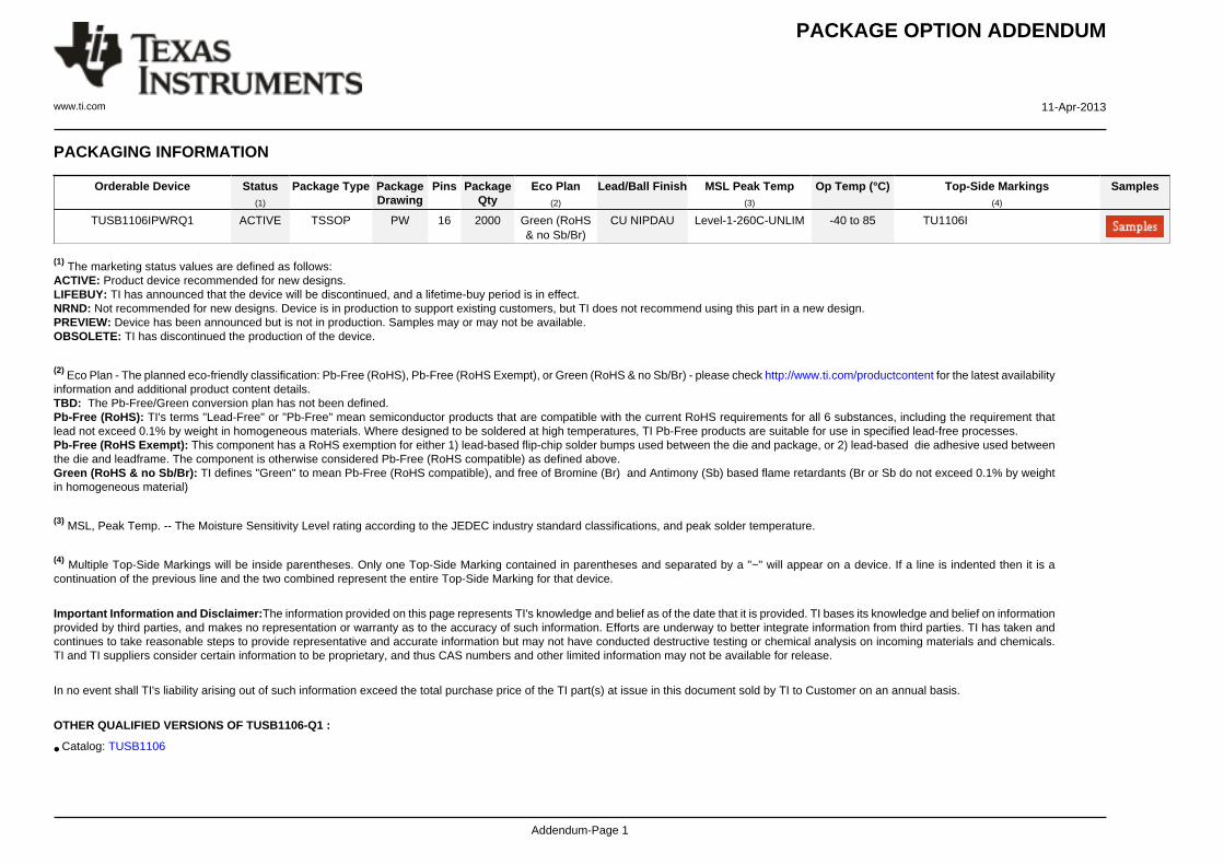
PACKAGING INFORMATION
Orderable Device Status(1)
Package Type PackageDrawing
Pins PackageQty
Eco Plan(2)
Lead/Ball Finish MSL Peak Temp(3)
Op Temp (°C) Top-Side Markings(4)
Samples
TUSB1106IPWRQ1 ACTIVE TSSOP PW 16 2000 Green (RoHS& no Sb/Br)
CU NIPDAU Level-1-260C-UNLIM -40 to 85 TU1106I
(1) The marketing status values are defined as follows:ACTIVE: Product device recommended for new designs.LIFEBUY: TI has announced that the device will be discontinued, and a lifetime-buy period is in effect.NRND: Not recommended for new designs. Device is in production to support existing customers, but TI does not recommend using this part in a new design.PREVIEW: Device has been announced but is not in production. Samples may or may not be available.OBSOLETE: TI has discontinued the production of the device.
(2) Eco Plan - The planned eco-friendly classification: Pb-Free (RoHS), Pb-Free (RoHS Exempt), or Green (RoHS & no Sb/Br) - please check http://www.ti.com/productcontent for the latest availabilityinformation and additional product content details.TBD: The Pb-Free/Green conversion plan has not been defined.Pb-Free (RoHS): TI's terms "Lead-Free" or "Pb-Free" mean semiconductor products that are compatible with the current RoHS requirements for all 6 substances, including the requirement thatlead not exceed 0.1% by weight in homogeneous materials. Where designed to be soldered at high temperatures, TI Pb-Free products are suitable for use in specified lead-free processes.Pb-Free (RoHS Exempt): This component has a RoHS exemption for either 1) lead-based flip-chip solder bumps used between the die and package, or 2) lead-based die adhesive used betweenthe die and leadframe. The component is otherwise considered Pb-Free (RoHS compatible) as defined above.Green (RoHS & no Sb/Br): TI defines "Green" to mean Pb-Free (RoHS compatible), and free of Bromine (Br) and Antimony (Sb) based flame retardants (Br or Sb do not exceed 0.1% by weightin homogeneous material)
(3) MSL, Peak Temp. -- The Moisture Sensitivity Level rating according to the JEDEC industry standard classifications, and peak solder temperature.
(4) Multiple Top-Side Markings will be inside parentheses. Only one Top-Side Marking contained in parentheses and separated by a "~" will appear on a device. If a line is indented then it is acontinuation of the previous line and the two combined represent the entire Top-Side Marking for that device.
Important Information and Disclaimer:The information provided on this page represents TI's knowledge and belief as of the date that it is provided. TI bases its knowledge and belief on informationprovided by third parties, and makes no representation or warranty as to the accuracy of such information. Efforts are underway to better integrate information from third parties. TI has taken andcontinues to take reasonable steps to provide representative and accurate information but may not have conducted destructive testing or chemical analysis on incoming materials and chemicals.TI and TI suppliers consider certain information to be proprietary, and thus CAS numbers and other limited information may not be available for release.
In no event shall TI's liability arising out of such information exceed the total purchase price of the TI part(s) at issue in this document sold by TI to Customer on an annual basis.
OTHER QUALIFIED VERSIONS OF TUSB1106-Q1 :
• Catalog: TUSB1106

PACKAGE OPTION ADDENDUM
www.ti.com 11-Apr-2013
Addendum-Page 2
NOTE: Qualified Version Definitions:
• Catalog - TI's standard catalog product

TAPE AND REEL INFORMATION
*All dimensions are nominal
Device PackageType
PackageDrawing
Pins SPQ ReelDiameter
(mm)
ReelWidth
W1 (mm)
A0(mm)
B0(mm)
K0(mm)
P1(mm)
W(mm)
Pin1Quadrant
TUSB1106IPWRQ1 TSSOP PW 16 2000 330.0 12.4 6.9 5.6 1.6 8.0 12.0 Q1
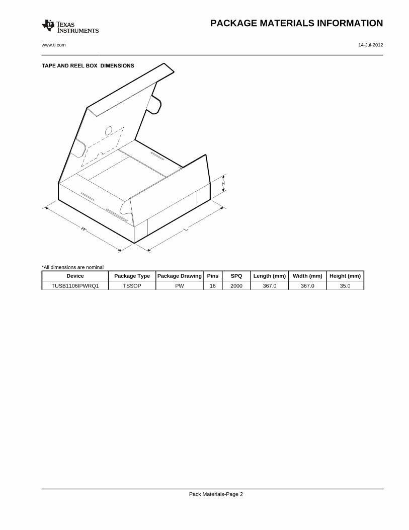
PACKAGE MATERIALS INFORMATION
www.ti.com 14-Jul-2012
Pack Materials-Page 1
*All dimensions are nominal
Device Package Type Package Drawing Pins SPQ Length (mm) Width (mm) Height (mm)
TUSB1106IPWRQ1 TSSOP PW 16 2000 367.0 367.0 35.0
PACKAGE MATERIALS INFORMATION
www.ti.com 14-Jul-2012
Pack Materials-Page 2

IMPORTANT NOTICE
Texas Instruments Incorporated and its subsidiaries (TI) reserve the right to make corrections, enhancements, improvements and otherchanges to its semiconductor products and services per JESD46, latest issue, and to discontinue any product or service per JESD48, latestissue. Buyers should obtain the latest relevant information before placing orders and should verify that such information is current andcomplete. All semiconductor products (also referred to herein as “components”) are sold subject to TI’s terms and conditions of salesupplied at the time of order acknowledgment.TI warrants performance of its components to the specifications applicable at the time of sale, in accordance with the warranty in TI’s termsand conditions of sale of semiconductor products. Testing and other quality control techniques are used to the extent TI deems necessaryto support this warranty. Except where mandated by applicable law, testing of all parameters of each component is not necessarilyperformed.TI assumes no liability for applications assistance or the design of Buyers’ products. Buyers are responsible for their products andapplications using TI components. To minimize the risks associated with Buyers’ products and applications, Buyers should provideadequate design and operating safeguards.TI does not warrant or represent that any license, either express or implied, is granted under any patent right, copyright, mask work right, orother intellectual property right relating to any combination, machine, or process in which TI components or services are used. Informationpublished by TI regarding third-party products or services does not constitute a license to use such products or services or a warranty orendorsement thereof. Use of such information may require a license from a third party under the patents or other intellectual property of thethird party, or a license from TI under the patents or other intellectual property of TI.Reproduction of significant portions of TI information in TI data books or data sheets is permissible only if reproduction is without alterationand is accompanied by all associated warranties, conditions, limitations, and notices. TI is not responsible or liable for such altereddocumentation. Information of third parties may be subject to additional restrictions.Resale of TI components or services with statements different from or beyond the parameters stated by TI for that component or servicevoids all express and any implied warranties for the associated TI component or service and is an unfair and deceptive business practice.TI is not responsible or liable for any such statements.Buyer acknowledges and agrees that it is solely responsible for compliance with all legal, regulatory and safety-related requirementsconcerning its products, and any use of TI components in its applications, notwithstanding any applications-related information or supportthat may be provided by TI. Buyer represents and agrees that it has all the necessary expertise to create and implement safeguards whichanticipate dangerous consequences of failures, monitor failures and their consequences, lessen the likelihood of failures that might causeharm and take appropriate remedial actions. Buyer will fully indemnify TI and its representatives against any damages arising out of the useof any TI components in safety-critical applications.In some cases, TI components may be promoted specifically to facilitate safety-related applications. With such components, TI’s goal is tohelp enable customers to design and create their own end-product solutions that meet applicable functional safety standards andrequirements. Nonetheless, such components are subject to these terms.No TI components are authorized for use in FDA Class III (or similar life-critical medical equipment) unless authorized officers of the partieshave executed a special agreement specifically governing such use.Only those TI components which TI has specifically designated as military grade or “enhanced plastic” are designed and intended for use inmilitary/aerospace applications or environments. Buyer acknowledges and agrees that any military or aerospace use of TI componentswhich have not been so designated is solely at the Buyer's risk, and that Buyer is solely responsible for compliance with all legal andregulatory requirements in connection with such use.TI has specifically designated certain components as meeting ISO/TS16949 requirements, mainly for automotive use. In any case of use ofnon-designated products, TI will not be responsible for any failure to meet ISO/TS16949.
Products ApplicationsAudio www.ti.com/audio Automotive and Transportation www.ti.com/automotiveAmplifiers amplifier.ti.com Communications and Telecom www.ti.com/communicationsData Converters dataconverter.ti.com Computers and Peripherals www.ti.com/computersDLP® Products www.dlp.com Consumer Electronics www.ti.com/consumer-appsDSP dsp.ti.com Energy and Lighting www.ti.com/energyClocks and Timers www.ti.com/clocks Industrial www.ti.com/industrialInterface interface.ti.com Medical www.ti.com/medicalLogic logic.ti.com Security www.ti.com/securityPower Mgmt power.ti.com Space, Avionics and Defense www.ti.com/space-avionics-defenseMicrocontrollers microcontroller.ti.com Video and Imaging www.ti.com/videoRFID www.ti-rfid.comOMAP Applications Processors www.ti.com/omap TI E2E Community e2e.ti.comWireless Connectivity www.ti.com/wirelessconnectivity
Mailing Address: Texas Instruments, Post Office Box 655303, Dallas, Texas 75265Copyright © 2015, Texas Instruments Incorporated