ADVANCED PROCESSING OF GaN FOR NOVEL ELECTRONIC...
202
ADVANCED PROCESSING OF GaN FOR NOVEL ELECTRONIC DEVICES By XIAN-AN CAO A DISSERTATION PRESENTED TO THE GRADUATE SCHOOL OF THE UNIVERSITY OF FLORIDA IN PARTIAL FULFILLMENT OF THE REQUIREMENTS FOR THE DEGREE OF DOCTORAL OF PHILOSOPHY UNIVERSITY OF FLORIDA 2000
-
Upload
nguyenkhuong -
Category
Documents
-
view
228 -
download
0
Transcript of ADVANCED PROCESSING OF GaN FOR NOVEL ELECTRONIC...

ADVANCED PROCESSING OF GaN FOR NOVEL ELECTRONIC DEVICES
By
XIAN-AN CAO
A DISSERTATION PRESENTED TO THE GRADUATE SCHOOL OF THE UNIVERSITY OF FLORIDA IN PARTIAL FULFILLMENT
OF THE REQUIREMENTS FOR THE DEGREE OF DOCTORAL OF PHILOSOPHY
UNIVERSITY OF FLORIDA
2000
ii
ACKNOWLEDGMENTS
I have been very fortunate to have the privilege of working with Prof. Stephen J.
Pearton, which turned out to be an exciting and rewarding learning experience. It is his
sharp insight, enlightened guidance and generous support that make it possible for me to
finish a project like this. He also took a genuine interest in my personal development and
ensured my growth by constant demands, advice and encouragement. I deeply appreciate
the best of opportunities Prof. Pearton provided me, and credit his belief in my capability
as an inspiration for achievement of my academic career. I am also indebted to Prof. Fan
Ren. The value of the academic and personal relationship with him is undeniable.
Many thanks extend to Prof. Cammy R. Abernathy, Prof. Fred Sharifi, Prof. Rajiv
K. Singh, and Dr. Jim M. Van Hove at SVT Associates, for their valuable contribution.
The assistance from my group mates and from collaborators of Prof. Ren's group and
Prof. Abernathy's group is highly appreciated.
Special thanks go to my family, without whom I would not be what I am, for their
moral support and encouragement through all my professional endeavors.
iii
TABLE OF CONTENTS ACKNOWLEDGMENTS ……………………………………………………………… . ii
LIST OF TABLES……………………………………………………………………... .. v
LIST OF FIGURES ……………………………………………………………………. vi
ABSTRACT …………………………………………………………………………… xiv
CHAPTERS
1. INTRODUCTION ……………………………………………………………….. .. 1
1.1 III-V Nitrides for Device Applications ……………………………………… .. 1 1.2 GaN Technology: A Late Blooming ………………………………………… .. 6 1.3 Processing Challenges for Novel Electronics ……………………………….. . 17 1.4 Dissertation Goal and Scope ………………………………………………… . 21
2. SEMICONDUCTOR PROCESSING: THEORY AND BACKGROUND
INFORMATION ……………………………………………………………... 23
2.1 Ion Implantation …………………………………………………………….. . 23 2.1.1 Ion Stopping and Damage Introduction ……………………………… . 23 2.1.2 Implant Isolation and Doping ………………………………………… . 27
2.2 Rapid Thermal Processing …………………………………………………... . 29 2.3 Metal/Semiconductor Contacts ……………………………………………… . 32
2.3.1 Schottky Contact ……………………………………………………... . 32 2.3.2 Ohmic Contact ……………………………………………………….. . 36
2.4 Dry Etching ………………………………………………………………….. . 40 3. ULTRA-HIGH TEMPERATURE ACTIVATION OF IMPLANT DOPING
IN GaN ………………………………………………………………………. . 47
3.1 Introduction …………………………………………………………………. . 47 3.2 High Temperature Annealing and AlN Encapsulation ……………………… . 48 3.3 N-type Implant Doping …………………………………………………….... . 54 3.4 P-type Implant Doping ………………………………………………………. . 57 3.5 Dopant Redistribution ……………………………………………………….. . 59 3.6 Residual Damage ……………………………………………………………. . 67

iv
4. HIGH RESISTANCE IMPLANT ISOLATION IN GaN ………………………... . 69
4.1 Introduction …………………………………………………………………. . 69 4.2 O-implantation for Selective Area Isolation ………………………………… . 71 4.3 Creation of High Resistivity GaN by Ti, Fe, and Cr Implantation …….……. . 76
5. ELECTRICAL CONTACTS TO GaN ……………………………………………. 82
5.1 Introduction ………………………………………………………………….. . 82 5.2 Effects of Interfacial Oxides on Schottky Contact ………………………….. . 85
5.2.1 (NH4)2S Treatment to Reduce Schottky Barrier Height ……………… . 85 5.2.2 Interfacial Insulator Model …………………………………………… . 92
5.3 Thermally Stable W-based Ohmic Contact …………………………………. . 95 5.3.1 W on Si-implanted GaN ……………………………………………… . 95 5.3.2 Behavior of W and WSi Contacts to p-GaN …………………………. . 98
6. DRY ETCH DAMAGE IN GaN ……………………………………………….... 107
6.1 Introduction …………………………………………………………………. 107 6.2 Plasma Damage in n-GaN …………………………………………………... 109
6.2.1 Comparison of N2 and H2 Discharge Exposure ……………………… 109 6.2.2 Effect of Etching Chemistries on Damage …………………………… 114 6.2.3 Thermal Stability of Damage ………………………………………… 124
6.3 Plasma Damage in p-GaN …………………………………………………… 126 6.3.1 Surface Type-Conversion Effects ………..…………………………... 126 6.3.2 Thermal Stability of Damage ………………………………………… 134
6.4 Determination of Damage Profile in GaN ………………………………….. 137 7. FABRICATION AND SIMULATION OF GaN-BASED BIPOLAR
TRANSISTORS …………………………………………………………….. 145
7.1 Introduction …………………………………………………………………. 145 7.2 Common Base Operation of GaN BJT and AlGaN/GaN HBT …………….. 147 7.3 Growth and Processing Issues ………………………………………………. 156 7.4 Quasi-3D Modeling of Electrical Performance of GaN Bipolar Transistors… 164
7.4.1 npn Structure …………………………………………………………. 166 7.4.2 pnp Structure …………………………………………………………. 176
8. CONCLUSIONS AND FUTURE TRENDS …………………………………….. 188 REFERENCES ……………………………………………………………………….. 193 BIOGRAPHICAL SKETCH …………………………………………………………. 202
xiv
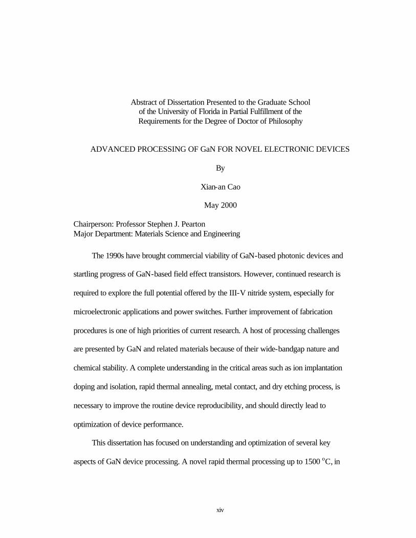
Abstract of Dissertation Presented to the Graduate School of the University of Florida in Partial Fulfillment of the Requirements for the Degree of Doctor of Philosophy
ADVANCED PROCESSING OF GaN FOR NOVEL ELECTRONIC DEVICES
By
Xian-an Cao
May 2000
Chairperson: Professor Stephen J. Pearton Major Department: Materials Science and Engineering
The 1990s have brought commercial viability of GaN-based photonic devices and
startling progress of GaN-based field effect transistors. However, continued research is
required to explore the full potential offered by the III-V nitride system, especially for
microelectronic applications and power switches. Further improvement of fabrication
procedures is one of high priorities of current research. A host of processing challenges
are presented by GaN and related materials because of their wide-bandgap nature and
chemical stability. A complete understanding in the critical areas such as ion implantation
doping and isolation, rapid thermal annealing, metal contact, and dry etching process, is
necessary to improve the routine device reproducibility, and should directly lead to
optimization of device performance.
This dissertation has focused on understanding and optimization of several key
aspects of GaN device processing. A novel rapid thermal processing up to 1500 oC, in

xv
conjunction with AlN encapsulation, has been developed. The activation processes of
implanted Si or Group VI donors, and common acceptors in GaN by using this ultrahigh
temperature annealing, along with its effects on surface degradation, dopant redistribution
and damage removal have been examined. 1400 degrees has proven to be the optimum
temperature to achieve high activation efficiency and to repair the ion-induced lattice
defects. Ion implantation was also employed to create high resistivity GaN. Damage-
related isolation with sheet resistances of 1012 Ω/ in n-GaN and 1010 Ω/ in p-GaN
has been achieved by implant of O and transition metal elements. Effects of surface
cleanliness on characteristics of GaN Schottky contacts have been investigated, and the
reduction in barrier height was correlated with removing the native oxide that forms an
insulating layer on the conventionally-cleaned surface. W alloys have been deposited on
Si-implanted samples and Mg-doped epilayers to achieve ohmic contacts with low
resistance, and better thermal stability than the existing non-refractory contact schemes.
Dry etching damage in GaN has been studied systematically using Schottky diode
measurements. Wet chemical etching and thermal annealing processes have been
developed to restore the ion-degraded material properties.
Based on these technical improvements, attempts have been made to demonstrate
GaN-based bipolar transistors. The devices operated in common base mode at current
densities up to 3.6 kA⋅cm-2 and temperatures up to 300 oC. The key issues which
currently limit the device performance, such as high base resistance, poor impurity
control, and defects resulting from the heteroepitaxial growth, have been addressed.
Physically-based simulation suggested that GaN bipolar devices may still suffer from
small minority-carrier lifetime in the absence of aforementioned processing problems.

1
CHAPTER 1 INTRODUCTION
1.1 III-V Nitrides for Device Applications
For the last three decades or so, the III-V semiconductor material system has been
viewed as highly promising for semiconductor device applications at blue and ultraviolet
(UV) wavelengths in much the same manner that its highly successful As-based and P-
based counterparts have been exploited for infrared, red and yellow wavelength. As
members of the III-V nitrides family, AlN, GaN, InN and their alloys are all wide band
gap materials, and can crystallize in both wurtzite and zincblende polytypes. Wurtizite
GaN, AlN and InN have direct room temperature bandgaps of 3.4 eV, 6.2 eV and 1.9 eV,
respectively (Fig. 1.1). In cubic form, GaN and InN have direct bandgaps, while AlN is
indirect. In view of the available wide range of direct bandgaps, GaN alloyed with AlN
and InN may span a continuous range of direct bandgap energies throughout much of the
visible spectrum well into the ultraviolet wavelengths. This makes the nitride system
attractive for optoelectronic device applications, such as light emitting diodes (LEDs),
laser diodes (LDs), and detectors, which are active in the green, blue or UV
wavelengths.1 Although similar applications based on InGaAlP heterostructures have
been successfully demonstrated, this material system is limited to about 550 nm. The
addition of III-V nitrides to the family of device-quality semiconductors is essential for
developing fall-color displays (Fig. 1.2) and the case of coherent sources high density
optical storage technologies, and very likely devices for signal and illumination

2
Fig. 1.1 Bandgap of hexagonal (α-phase) and cubic (β-phase) InN, GaN, and AlN and their alloys versus lattice constant a0.
Fig. 1.2 The various ternary and quarternary materials used for LEDs with the wavelength ranges indicated.
900 800 700 600 500 400
Wavelength (nm)
R O Y G B V
GaNGaP
InN
InGaN
AlPInP
AlAsAlGaAs
GaAs
InGaAlP
Wurtzitie Zincblende
β-AlN
β-GaN
β-InNα-InN
α-GaN
α-AlN
300 K
Lattice Constant (Å)
Ban
dgap
Eg
(eV
)

3
application. Particularly, the combination of GaN-based blue and green LEDs with
GaAs-based red LEDs forms the basis for large-scale full displays and white light
illumination. The solid-state white light source generated by mixing the primary colors in
a light scrambling configuration would provide not only compactness and high lifetime,
but also would reduce power consumption by 80-90% compared to incandescent or
fluorescent light sources.
Another area gaining a lot of attention for III-V nitrides is high temperature/high
power electronics.2 The interest stems from two intrinsic properties of this group of
semiconductors. The first is their wide bandgap nature. The wide bandgap materials such
as GaN and SiC, are promising for high temperature applications because they go
intrinsic at much higher temperatures than materials like Ge, Si and GaAs. It means that
GaN power devices can operate with less cooling and fewer high cost processing steps
associated with complicated structures designed to maximize heat extraction. The second
attractive property of III-V nitrides is that they have high breakdown fields. The critical
electric field of the breakdown scales roughly with the square of the energy band gap, and
is estimated to be >4 MV/cm for GaN,3 as compared to 0.2 and 0.4 MV/cm for Si and
GaAs respectively. Fig. 1.3 is a plot of avalanche and punch through breakdown of GaN
Schottky diodes calculated as a function of doping concentration and standoff layer
thickness. It can be seen that 20 kV device may be obtained with ~100 µm thick GaN
layer with doping concentration <1015 cm-3.
GaN has also excellent electron transport properties, including good mobility, and
high saturated drift velocity as shown in Fig. 1.4.4 This makes it adequate for general

4
Fig. 1.3 Calculated breakdown voltage as a function of doping concentration and
thickness of the drift region in GaN M-n--n+ diodes.
Fig. 1.4 Electron drift velocity at 300 K in GaN, SiC, Si and GaAs computed using the
Monte Carlo technique.
Drift Region Doping Concentration (cm-3)
1013 1014 1015 1016 1017
Bre
akdo
wn
Vol
tage
(V
)
101
102
103
104
105
106
100 µ
20 µ
5 µ
1 µ
GaN Diode
Thickness
8
Avalanche BD
Punch-through BD

5
electronics, and promising for microwave rectifiers, particularly. The material properties
associated with high temperature, high power, and high frequency application of GaN
and several conventional semiconductors are summarized in Table 1.1. It is anticipated
that GaN may eventually prove to be superior to SiC in this area.
Table 1.1 Comparison of 300 K semiconductor material properties. ( CFOM= Combined Figure of Merit for high temperature/high power/high frequency applications)
Property Si GaAs 4H-SiC GaN
Bandgap Eg (eV) 1.12 1.42 3.25 3.40
Breakdown Field EB (MV/cm) 0.25 0.4 3.0 4.0
Electron Mobility µ (cm2/V⋅s) 1350 6000 800 1300
Maximum Velocity νs (107 cm/s) 1.0 2.0 2.0 3.0
Thermal Conductivity χ (W/cm⋅K) 1.5 0.5 4.9 1.3
Dielectric Constant ε 11.8 12.8 9.7 9.0
CFOM = χεµνsEB2/(χεµνsEB
2)Si 1 8 458 489
The strongest feature of the III-V nitrides compared to SiC is the heterostructure
technology it can support. Quantum well, modulation-doped hetero-interface, and
heterojunction structure can all be made in this system, giving access to new spectral
regions for optical devices and new operation regimes for electronic devices. From this
point of view, III-V nitrides can be considered the wide band gap equivalent of the
AlGaAs/InGaAs system which has set the modern benchmark for microwave device
performance.

6
Other advantageous properties of III-V nitrides include high mechanical and
thermal stability, large piezoelectric constants and the possibility of passivation by
forming thin layers of Ga2O3 or Al2O3 with band gaps of 4.3 eV and 9.2 eV respectively.
In addition, AlN has received considerable attention for its insulating property,5
particularly as a potential isoelectronic insulator for GaAs field effect transistors (FETs).
1.2 GaN Technology: A Late Blooming
Substantial research on III-V nitrides growth was initiated in early 1960s. However,
they have trailed way behind the easier-to-grow Si and GaAs semiconductors on the
development curve. Nearly 30 years later, Si and GaAs have been pushed to their
theoretical limits, while nitrides are just beginning to show their promise. The
technological spin-offs came late because ideal substrates could not be found and the
consequent growth of GaN thin films contained substantial concentration of defects and
had high n-type background. Even in films having relatively small background electron
concentration, p-type doping could not be achieved until recently.
One particular difficulty in the growth of GaN thin films is the unavailability of
sufficiently large (>1 cm) single crystals for use as substrate for homoepitaxial growth.
Thus up to now, heteroepitaxial growth has been a practical necessity and the choice of
substrate is critical. Possible substrate materials should have low thermal expansion and
lattice mismatch with the grown crystals. Also, they should be unaffected by the growth
chemistries (such as NH3 or H2) at high growth temperatures (in excess of 1000 oC in
some cases). Under these presuppositions, sapphire and SiC are the most popular
substrate materials used currently. When hexagonal GaN is grown on the (0001) basal

7
plane of Al2O3, a lattice misfit of ~13% at the growth temperatures can generate high
density of dislocations and defects in the thin film. In the practical case, a large part of
the misfit is relaxed through 3D island growth. The residual strain is comparable to the
lattice misfit between 6H-SiC and GaN, and result is comparable dislocation densities
observed.6 Today, SiC substrates, though more costly, are of increasing interest for high
temperature high power devices like transistors due to their good thermal conductivity
and possibility of n- and p-type doping. The materials with a close lattice match with
GaN, such as LiAlO2 7 and LiGaO2
8, were also used for epitaxial substrates. However,
the grown GaN lacked the desired electronic properties due to either the rough growth or
unintentional contamination from the substrates. The ideal candidate substrate is clearly a
GaN wafer. Several research groups are investigating the growth of the bulk GaN crystals
and very thick films through various techniques.9-11 However, commercially available
large area GaN wafers appear to be several years away. The nitride community is
therefore challenged with growth of heteroepitaxial films.
Many epitaxial thin film growth processes have been developed, including
molecular beam epitaxy (MBE),12,13 hydride vapor phase epitaxy (HVPE),9-11,14
metalorganic chemical vapor deposition (MOCVD),15-20 and derivatives of these
methods. In the past few years, MOCVD has evolved into a leading technique for
production of III-V nitrides optoelectronic and microelectronic devices. One remarkable
application worthy to be mentioned is the achievement of super-bright blue LEDs.18
Characteristics of this method include the use of high purity chemical sources, a high
degree of composition control and uniformity, high growth rates, large scale
manufacturing potential and the ability to grow abrupt junctions.

8
Initially the growth of GaN was performed directly on sapphire and SiC substrate,
with large crystalline defects threading vertically from the substrate interface through the
newly deposited thin film. The wafer usually had rough surfaces mainly caused by the 3D
growth mode. In 1986, Amano et al.16 succeeded in remarkably improving the GaN
surface morphology as well as the electrical and optical properties by deposition of a thin
low-temperature AlN buffer layer prior to the high temperature growth of GaN. The
essential role of this buffer is both to supply nucleation and promote lateral growth of the
GaN film due to the decrease in interfacial free energy between the film and the substrate.
Although the buffer layer has reduced the effects of the lattice mismatch, the densities of
the threading defects in these thin films are still in the range of 109-1010 cm-2, and on the
order of one million times higher than in other semiconductor systems. These defect-
laden materials, to date, have had a surprisingly small effect on the performance of both
optical and electronic devices, but they may raise major questions as to the long-term
stability of these devices. It is unlikely that the full promise of GaN and related alloys can
be realized without a major reduction in the defect densities in the as-grown materials.
In 1994, the lateral epitaxial overgrowth (LEO) technique was employed to further
improve the quality of the heteroepitaxially grown GaN by a marked reduction in defect
density.19 In this method, a layer of GaN grown by MOCVD is covered with 100-200 nm
of amorphous SiO2 and Si3N4 with ex situ techniques. Small circular or rectangular
"windows" are then etched through to the underlying GaN. A GaN film is subsequently
regrown under conditions such that growth occurs epitaxially only in the windows and
not on the mask. If growth continues, lateral growth over the mask eventually occurs.
Since most of the extended dislocations propagate in the growth direction through GaN,

9
very few threading dislocations are visible in the regrown GaN that extends laterally over
the mask. Marchand et al.20 observed that the density of dislocation reaching the surface
of LEO GaN was in the 104-105 cm-2 range, while the film over the window regions still
contained high levels of the threading defects. Fig. 1.5 compares the cross-section
transmission electron microscopy (TEM) of a typical MOCVD growth and LEO GaN.
Fig. 1.5 Cross section TEM of typical MOCVD grown GaN using an AlN buffer layer on SiC (left) and typical LEO GaN (right).
A refined approach to a nearly dislocation free GaN substrate for devices can be
employed by two successive LEO steps with the mask of the second step positioned over
the opening defined by the mask of the first step, thus blocking the defects that grown out
of the first windows. This complicated procedure offers the possibility of eliminating the
disadvantages of heteroepitaxy, and will be important until GaN substrates become
available.

10
In addition to growing GaN films with low defect densities, another key
requirement for fabricating devices is the ability to precisely control the desired electrical
properties of the thin film. In general, wide bandgap semiconductors are difficult to dope
due to native defects. When the enthalpy for defect formation is lower than the band gap
energy, the probability of generating a defect increases with the bandgap, i.e. the energy
released by donor-to-acceptor transition. Particularly for GaN, MOCVD grown material
is commonly n-type conductive, and N-vacancy was long believed to be the dominant
donor. Many attempts have been made to avoid N-vacancy formation by growing GaN at
high pressures and high temperatures.21,22 Efficient n-type doping of GaN through
incorporation of Si during the growth proved relatively easy to achieve. Highly doping
can also be created by implantation of Si or Group VI donors. Recently, Burm et al.23
have shown a shallow Si implant at high dose to produce a doping density of 4×1020 cm-3,
resulted in an extremely low ohmic contact resistance of 4×10⁻⁸ Ω⋅cm2 using Ti/Au
contacts.
Since conductivity is proportional to the product of carrier concentration and Hall
mobility, another goal for GaN used in device applications is to obtain highest Hall
mobilities possible. Fig. 1.6 summarizes the measured electron mobility in n-type GaN,
along with the results obtained from Monte Carlo simulation.24,25 As can be seen, the
experimental data is roughly half of the calculated value, possibly due to significant
scattering from impurities and defects in the state-of-the-art materials.
The III-V nitrides are expected to be made p-type by inserting Column II elements
such as Zn, Mg Be and Ca substutionally for Ga to form single acceptors. However all of
these divalent elements form deep acceptors, the shallowest being Mg with an ionization

11
Fig. 1.6 A survey of 300 K GaN electron Hall mobility values as reported by various groups. The solid line shows the calculated results for uncompensated n-GaN.
level of 0.17 eV which is still many kTs above the valence bandedge of GaN.26 At this
acceptor level, one should only expect <10% of the Mg atoms to be ionized at room
temperature, which means the Mg concentration needs to be approximately two orders of
magnitude larger than the desired hole concentration. When MOCVD is used as the
growth method, it has been difficult to obtain p-type conductivity. It was later found that
hydrogen plays a crucial role in passivating the Mg acceptors, and creates a neutral
complex Mg-H that prevents the formation of holes in GaN.27 It was first shown by
Amano et al.28 that p-type conductivity can be achieved by activating Mg-doped GaN
using low-energy electron irradiation. Nakamura demonstrated subsequently that the
activation of Mg can also be realized by thermal annealing at ~700 oC.29 Note that MBE
Electron Concentration (cm-3)
1015 1016 1017 1018 1019 1020 1021
300
K E
lect
ron
Mob
ility
(cm
2 V-1
s-1)
100
1000 Wurtzite GaN

12
grown GaN doped with Mg may be p-type without a thermal activation process, because
of the absence of hydrogen and H-N radicals during growth. In addition, p-type doping
was also achieved by implant of Ca or Mg into GaN, followed by high temperature
annealing (~1100 oC).30,31 The highest hole concentration reported so far is ~1018 cm-3,
and the typical hole mobility is very low, often 10 cm2⋅V-1⋅s-1 or below, but allowing the
realization of p-n junctions. Achieving low resistance ohmic contacts to the GaN layers
with poor p-type doping concentrations has proved to be troublesome. Recently, Brandt
et al.32 found that by compensating Be with O, a neutral dipole is formed that does not
scatter the holes. Hence a record high hole mobility of 150 cm2⋅V-1⋅s-1 was obtained. This
may be the ideal contact layer for GaN based devices.
The current level of the progress in the development of GaN commercially viable
devices, namely GaN based-LEDs, LDs and UV detectors, has been the direct result of
the realization of high quality crystals of GaN, AlGaN, InGaN, and relatively recent
achievement of p-type conduction in GaN. The first pn junction LED was demonstrated
by Amano et al.28 in 1989. Following this , Nichia Chemical Industries announced the
commercial availability of blue LEDs with high efficiency and luminous intensities over
1 cd.18 In the subsequent years, high brightness single quantum well structure blue, green,
and yellow InGaN LEDs with luminous intensities above 10 cd have been
commercialized.33,34 In 1996, Nakamura et al.35 reported the first current-injection GaN-
based LDs with separate confinement heterostructure, and subsequently achieved
continuous-wave (CW) lasing at room temperature.36 Fig. 1.7 schematically shows the
cross-section of the nitride-based laser diode. The active layer is a InGaN multiquantum
well with a large number of well layers. GaN and AlGaN were used as the waveguide

13
and cladding layers, respectively. The mirror facet was formed by numerous methods,
including dry etching, polishing or cleaving.
Fig. 1.7 Cross-sectional view of a typical structure of GaN-based laser diode.
Surprisingly, the high-density dislocations resulting from the heteroepitaxial growth
on sapphire in these optical devices did not appear to be efficient nonradiative centers, as
they are in other III-V materials. However, the crystalline defects do affect the device
reliability. Nichia employed the LEO growth technique for their blue LDs and achieved
an increase in device lifetime from a few hundred hours to an estimated 10,000 hours.37
Another major problem limiting diode performance is high specific contact resistance of
(0001) sapphire subatrate
n-GaN:Si
n-contact (Ti/Al)
LT GaN buffer
p-contact (Ni/Au) p-GaN:Mg p-contactp-AlGaN:Mg cladp-GaN:Mg waveguideInGaN QWs activen-GaN:Si waveguiden-AlGaN:Si cladn-GaN:Si n-contact

14
ohmic contact on the p-GaN side of the junction. Present lateral GaN lasers suffer
significant IR drops due to poor p-type doping and ohmic metallization.
The nitride material growth technology that supports the optical device efforts has
also proven to be compatible with the development of electronic devices. In the past
several years, the electronic device development has emphasized field effect transistor
(FET) structures, because this important class of devices put smaller demands on the
growth and fabrication technique compared to bipolar transistors. The rapid progress that
has been made, especially in modulation-doped FETs (MODFETs), has been sufficient to
show that GaN and related alloys will play a significant role in the future development of
high temperature, high power, and high frequency electronic devices.38-41
Fig. 1.8 presents a schematic representation of a GaN/AlGaN heterostructure. Due
to the large conduction band discontinuity, the electrons diffusing from the large bandgap
AlGaN into the smaller bandgap GaN form a 2D electron gas (2DEG) in the triangle
quantum well at the interface, which is the hallmark of MODFET. The sheet carrier
density of the 2DEG was found to be further enhanced by the strong pizeoelectronic
effect in GaN. Pizeoelectronic coefficients in nitrides were measured to be about an order
of magnitude higher than in traditional Group III-V semiconductors.42 Theoretical
simulations have predicted a high peak electron velocity of ~3×107 cm/s 25 and an
electron mobility of ~2000 cm2⋅V-1⋅s-1 in the GaN channel at room temperature at a
carrier concentration of 1017 cm-3.43 Gaska et al.4 investigated the highest measured Hall
mobility at room temperature was 2019 cm2⋅V-1⋅s-1, and increased approximately fivefold
to 10,250 cm2⋅V-1⋅s-1 below 10 K for growth on 6H SiC substrate.

15
Fig. 1.8 Conduction band structure of a modulation-doped structure.
In 1993, Khan et al.38 demonstrated the first AlGaN/GaN MODFET, with a gm of
23 ms/mm and 2DEG mobility of 563 cm2⋅V-1⋅s-1 at 300 K. They also reported the first
microwave results with ft of 11 GHz and fmax of 14 GHz.39 In the early stages, the
MODFETs exhibited very low transconductances and relatively poor frequency response.
This is consistent with the defect-laden nature of the early GaN and AlGaN layers. With
improvements in the materials quality, the transconductance, current capacity, drain
breakdown voltage are all increased to the point that GaN-based MODFETs are now
strong contenders in the arena of high power devices/amplifiers. To date, the highest
power density achieved for a 0.45×125 µm GaN MODFET is 6.8 W/mm at 10 GHz and
associated gain of 10.65 dB.40 The operation temperature has been pushed to 750 oC by
employing a thermally stable Pt/Au gate contact.41
The published performances of epitaxial GaN-based MESFETs demonstrate that all
the required components for a MESFET based technology are in place,44,45 i.e. an
ECEC
∆EC
EFE0
E1+
++
++
ED
AlGaN GaN
2DEG

16
appropriate high resistivity buffer/substrate combination has been developed for doped
layer epitaxial growth, FET channels can be grown with thin n+ contact layers on which
ohmic contact with adequate contact resistances have been achieved, gate metalizations
which can pitchoff the channel and support a high drain bias have been demonstrated,
and it has shown that both mesa etch and implant isolation can be used to define the
active device area. Recently, an all implanted GaN junction FET,46 a Si3N4 gated GaN
MISFET,47 and a Ga2O3(Gd2O4) gated GaN MOSFET 48 with reasonable performance
were also reported. These types of devices potentially have advantage over MESFET,
especially at high temperatures due to low reverse leakage currents.
So far, there are only several reports of development of GaN based bipolar
transistors.49,50 Basically the device performance is limited by the difficulty in growth and
processing related to the buried p-type layer and the small minority carrier lifetime. It is
still far from commercialization of these devices, but their developments will follow the
material improvements in the new decade, and much impetus comes from defense
applications where ultrawide bandwidth and linearity are desired.
Group III-V nitrides offer a valuable combination of electrical, optical and
pizeoelectrical behavior, and enable the fabrication of LEDs, LDs, detectors, and
transistors. In the past, the poor quality of the materials, the lack of p-type doping, and
the absence of reliable processing procedures thwarted engineers and scientists from
fabricating these useful devices. However, the 1990s have brought significant advances
in the sophistication of growth techniques, the purity of the chemicals used for film
deposition, the controlled introduction and activation of selected impurities, and progress
in processing techniques. Most of the aforementioned obstacles have been sufficiently

17
overcome, and the electronic and optical devices have been demonstrated and partially
commercialized. Market projections show that GaN-based blue and green LEDs will
represent the majority of the estimated $3 billion per year GaN-based device market by
2006. In transistors, GaN can go where no other semiconductors have gone before. The
future development in this area will definitely be fueled by the increasing demand for
high temperature, high power applications. From materials science to device engineering,
from laboratory research to commercial products, III-V nitride technologies have shown a
late but exciting blooming.
1.3 Processing Challenges for Novel Electronics
While further improvements in the III-V nitride materials quality can be expected to
enhance device operation, further device advances will also require improved processing
technology. Owing to their wide bandgap nature and chemical stability, GaN and related
materials present a host of device processing challenges, including poor p-type doping
(by implantation), difficulty in achieving reliable low-resistance p-ohmic contacts, high
temperatures needed for implant activation, lack of efficient wet etch process, generally
low dry etch rates and low selectivity over etching masks, and dry etch damage. These
problems constitute a major obstacle to successful demonstration and commercialization
of some GaN-based devices, such as bipolar transistors and power switches, whose
performance are much more affected by the immature fabrication techniques. To fully
exploit these device applications, a number of critical advances are necessary in the areas
of implantation doping and isolation, high temperature thermal processing, ohmic contact
to p-type material, dry etching process, and device passivation.

18
Ion implantation is an enabling technology for creating selective area doping and
forming high resistance regions in device structures. For the development of ion
implantation doping for advanced GaN-based electronics, it is important to understand
the dopant activation process, and implantation-induced damage generation and removal.
Recent studies have showed that quite good activation efficiency can be obtained by
annealing at 1100 oC anneal,30,51 but implantation damage can not be significantly
removed at this temperature. Annealing at temperatures >1300 oC are suggested to fully
remove the damage and further optimize the transport properties of implanted regions in
GaN.51 Since these temperatures are beyond the capability of most rapid thermal
annealing systems, new annealing apparatus must be developed. Consequently, there is
an urgent need to carry out detailed studies on the dopant activation, impurity
redistribution, defect removal, and surface degradation at these elevated temperatures.
Efficient surface protection must be developed to prevent material decomposition and N2
loss from the GaN surfaces.
Ion implantation is also attractive for inter-device isolation and producing current
guiding. Efficient compensation has been achieved in the GaN materials by using N or
He implantation.30,52 However, the isolation is not stable at high temperatures, i.e. typical
implant damage compensation. Implantation in In-containing III-V nitrides has shown
that InGaN, as used in LED, laser cavity, or transistor channel, is difficult to be rendered
highly resistive.53 The defect level is usually high in the energy gap, not near midgap, as
is ideal for implant isolation. There is a strong need for an understanding of the implant
isolation process and mechanism in III-V nitride materials because of the emerging
applications for high temperature, high power electronics based on this material system.
19
In particular, attempts need to be made to explore thermally stable implant isolation in
GaN, and significant compensation must be achieved in the In-containing nitrides.
Considerable progress in the development of contacts to GaN has been made in the
past several years.54 Nevertheless, it is necessary still to improve upon the electrical
performance of these contacts, particularly to achieve low contact resistances to p-GaN,
and to develop contacts with greater thermal stability, which is critical for high current
density devices. It has proven challenging to obtained acceptable low specific contact
resistances on p-GaN. Values ≤10-5 Ω⋅cm2 would be desirable in general for electronics,
but more typical numbers are 10-1-10-3 Ω⋅cm2. The high contact resistances can be
attributed to several factors, including: (1) The absence of a metal with a sufficiently high
work function (the bandgap of GaN is 3.4 eV, and the electron affinity is 4.1 eV, but
metal work functions are typically ≤ 5 eV). (2) The relatively low hole concentrations in
p-GaN due to the deep ionization level of the Mg acceptor (~170 meV). (3) The tendency
for the preferential loss of nitrogen from the GaN surface during processing, which may
produce surface conversion to n-type conductivity. In order to further lower the contact
resistances to p-GaN, it will be necessary to further increase p-type conductivity or to
lower the barrier height of the metal contacts, perhaps by growing a more readily
contacted compositionally graded semiconductor alloy on the p-GaN.
The thermal stability of the contacts is also noteworthy. Annealing at ~700 oC
resulted in interfacial reaction along with serious morphological degradation of the
conventional Ti-based or Ni-based contacts.55,56 In the case of contact to p-GaN, the
metallization will heat up as current flows across the interface due to the high series
resistance, leading to metal migration down threading dislocations and eventual shorting

20
of the devices. Thermally stable Schottky contacts are also required for power amplifiers
and optoelectronics that operate at high temperatures, but the electrical characteristcs of
the metal/n-GaN diodes have been reported to suffer degradation upon exposure to
temperatures as low as 300 oC (Pd),57 400 oC (Pt),58 575 oC (Au)59 and 600 oC (Ni).54
Furthermore, there is a large scatter in the measured results of Schottky barrier
height (SBH) and the ohmic contact resistance, suggesting that our understanding of the
interface reactions, surface preparation, and non-idealities associated with the metal/GaN
contacts is far from complete.
Dry etching has become the dominant patterning technique for the Group III
nitrides due to the shortcomings in wet chemical etching. The etch rates in reactive ion
etch (RIE) systems are generally low.60 High density plasma etching, i.e. inductively
coupled plasma (ICP)61,62 and electron cyclotron resonance (ECR)63 etching have been
developed in a variety of chlorine- and methane-based chemistries. The etch rates of GaN
were reported as high as 9800 Å/min in a Cl2/H2/Ar mixture.62 However, surface
roughening, N depletion, and degradation in electrical and optical properties were
observed. Some device etching applications, such as gate recessing for FETs and base
mesa formation for HBTs, can be particularly susceptible to ion-induced damage. In
order to minimize the deleterious effects of energetic ions during dry etching, it will be
necessary to develop effective low-damage etching processes that utilize ion energies
well below 100 eV. At this point, it is also important to determine the nature of the
plasma-induced damage in GaN, and to explore the procedures for damage removal.
GaN-based amplifiers and switches are attractive for high power applications in
hostile environments. Reliable edge termination and passivation process are critical to

21
fully exploit these types of devices. There is not much work to date in this area. In
addition, as discussed earlier, thermally stable doping, isolation, and metal contacts are
all key issues for these special applications.
1.4 Dissertation Goal and Scope
This dissertation will investigate several important aspects of GaN processing.
Emphasis will be placed on achieving high activation efficiency implant doping and high
resistance implant isolation, developing ultra-high temperature thermal processing,
achieving reliable low resistance ohmic contacts, and systematic study of dry etch
damage. All the work is directed towards the optimizing the fabrication techniques of
GaN-based optoelectronics and microelectronics. Particularly, fabrication of advanced
GaN-based bipolar transistors will be attempted, based on these improved process
modules. Finally, the simulation of the device performance will be performed as the
implication for future trends in the arena.
Chapter 2 presents the physical mechanisms of several aspects of semiconductor
processing, including ion implantation, rapid thermal annealing, metal contact, and dry
plasma etching. The related background information of III-V materials are reviewed.
Chapter 3 starts with a review of efforts to develop implant doping in GaN to date.
An novel rapid thermal processing up to 1500 oC is then developed, with AlN as
encapsulation. The activation processes of implanted donors and acceptors in GaN using
this ultra-high temperature annealing, along with its effects on surface degradation,
impurity redistribution and defect removal are examined.

22
Chapter 4 discusses implantation isolation in n- and p-type GaN, with emphasis on
comparison of the behavior of implanted O and transition metal elements like Fe, Cr and
Ti in GaN. The compensation mechanism and the damage-related levels are determined.
In Chapter 5, early studies on ohmic contact and Schottky contact to GaN are
reviewed. Then a new surface cleaning process using an additional (NH4)2S treatment is
developed. The thin native oxide left after conventional cleaning is found to have a strong
influence on the contact characteristics on GaN. Finally the behavior of W-based ohmic
contacts on both Si-implanted n-type GaN and Mg-doped p-type GaN is studied. The
refractory contact schemes prove to be much more thermally stable than the more
common metallizations.
Chapter 6 presents a systematic study of the effects of ICP Ar, H2, N2, and Ar/Cl2
discharge exposure on the electrical properties of n- and p-type GaN. The thermal
stability and depth of the plasma damage are determined. Two different techniques are
developed to remove dry etch damage, i.e. wet chemical etching and thermal annealing.
In Chapter 7, the developed process modules are employed to demonstrate the first
MBE grown GaN BJT and AlGaN/GaN HBT. The devices operate at high temperatures
and high powers in common-base mode. The key issues related to structure growth and
device fabrication are addressed. Finally, in order to gain a better understanding of the
expected performance of GaN-based bipolar transistors, and as a suggestion for further
work, physically-based simulation is performed using Atlas/Blaze.
Chapter 8 offers conclusions of the current work and an outlook for the future
research.

23
CHAPTER 2 SEMICONDUCTOR PROCESSING: THEORY AND
BACKGROUND INFORMATION
2.1 Ion Implantation
2.1.1 Ion Stopping and Damage Introduction
Ion implantation has played a major role in development of III-V semiconductor
device technology. It is used to create the active layers by implanting a dopant species
and then activating the dopant by high temperature anneal. The bombardment with
energetic ions can also be utilized to create a high resistivity region selectively on a wafer
that already contains doped layers.
The ion implanted into a semiconductor undergoes collisions with the target atoms,
and loses energy due to the ion stopping process. Much of the ion energy is transferred to
the lattice, as a localized thermal spite or to displace the target atoms. The total energy
loss per unit distance is determined by two effects: the electronic stopping and the nuclear
stopping. In the former process, the ion energy is lost by excitation and ionization of
atoms, which suffer an inelastic collision with the ion. The lost energy eventually
dissipates as heat, and does not create atomic displacements in the materials. The
electronic stopping cross section is proportional to the velocity of the implanted ion and
therefore to the square root of its energy. Its contribution dominates in the high-energy
regime. Nuclear stopping occurs as a result of elastic collisions of ions with nuclei or
whole atoms in the solid, in which, a part of kinetic energy of the incoming ion is

24
transferred to displace the nuclei absorbed this impart. These displaced nuclei may also
have enough energy to displace other nuclei, leading to a cascade of recoiled atoms.
Nuclear energy loss dominates at intermediate energies, and leads to the creation of deep-
level compensating defects. At high energies, the contribution from this process tends to
be small because fast ions have only a short time to interact with a target nucleus, and
cannot transfer energy efficiently. Fig. 2.1 shows a schematic of the relative energy loss
due to electronic and nuclear stopping processes as a function of ion energy.64 The
relative importance of these two stopping mechanisms also depends on the mass of the
implanted ions, the mass and atomic density of the target.
Fig. 2.1 Schematic of the cross section S (proportional to the energy loss per unit distance) for electronic (Se) and nuclear (Sn) stopping processes as a function of ion
energy. Typical values for the parameters E1, E2 and E3 for O implanted in GaAs are: E1=10 keV, E2=20 keV, E3=4 MeV.

25
Both the stopping effects produce an energy loss rate of some tens of eV per
angstrom in semiconductors. The total value of dE/dx is roughly constant for many ions
over the ranges of energies of interest for implantation. The projected range Rp is then
essentially proportional to the initial incident ion energy. With an amorphous target
material, the ion profile follows purely Gaussian stopping distribution, which is related to
the projected range Rp, standard deviation ∆Rp and implant dose Φ:
N( x ) = Φ∆ ∆2 2
2
2π R
x R
Rp
p
p
exp[( )
]−−
(2.1)
The peak concentration Np=Φ∆2π Rp
occurs at Rp, and N ( )xN
ep= at x R Rp p= ± ∆ .
Considering the single crystal nature of the target, the channeling effect must be taken
into account. Channeling takes place when implanted ions enter regions between rows of
atoms, so that few nuclear collisions occur. The ions penetrate much deeper under these
conditions than for implantation in a random direction, leading to large tails on the
substrate side of the final profiles. It is better described by using joined Gaussians or by
taking into account higher order moments such as skewness and kurtosis. Channeling can
be minimized by rotating and tilting the sample with respect to the beam direction. The
only completely effective method to eliminate it is to preamorphize the semiconductor.
This is a successful procedure for implantation in Si, but is not appropriate for III-V
materials.64
Light ions slow down initially primarily by electronic stopping with little
displacement damage until eventually nuclear stopping becomes dominant at the end of
this range. By contrast, heavy ions undergo a relatively higher degree of nuclear stopping,
displacing target atoms right from the surface inwards, producing collision cascades,
26
leading to considerable lattice damage within a small volume. Depending on the ion, the
dose, and the implant temperature, the implant damage can consist of either amorphous
layers or extended crystalline defects (dislocations and stacking faults). In III-Vs damage
accumulation and possible amorphization are modeled by either a heterogeneous
mechanism, in which individual damage clusters are considered to be amorphous and
overlapping of these regions results in complete amorphization (heavy ions), or a
homogeneous mechanism in which the crystal becomes unstable and collapses to an
amorphous state when the defect density reaches a critical value (light ions). Since ions
require certain threshold energy for the production of damage, the maximum of damage
distribution is always closer to the surface than that of the ion profile. Note that for a
particular ion to completely penetrate a doped semiconductor layer and render it semi-
insulating, it is the ion damage profile that is important, not the ion profiles itself. Both
the damage profile and dopant profile can be simulated by Monte Carlo calculations of
energy deposition given up in atomic stopping processes.
In III-V semiconductors implantation can also lead to the creation of regions with
local deviations from stoichiometry resulting from the different displacement properties
of the lattice constituents, which have unequal masses.64,65 The lighter element recoils
further, resulting in an excess of the heavier elements near the surface and an excess of
the lighter elements at greater depths. Repair of the lattice during subsequent annealing
requires displaced atoms diffusing back to appropriate sites. However, in III-V’s, the
displaced atoms are unable to move quickly enough to keep up with the regrowth front,
leading to highly twinned materials. The electrical activation in regrown material is
significantly worse due to the remnant disorder than if amorphization is avoided. The

27
formation of an amorphous layer can be prevented through elevated-temperature
implantation, where more point defects are able to recombine and annihilate each other
due to higher mobility. At very high dose rates, the sample may heat up, resulting in
dynamic annealing, in which case an amorphous layer may never form. It has been
observed that GaN has a very high threshold of amorphization, on the order of ~1016 cm-2
(Si implant, 100 keV).66 This is in sharp contrast to GaAs where an amorphous region
forms for room temperature implants near a dose of ~1014 cm-2,67 and amorphization of
InP occurs at even lower ion doses(~1013 cm-2).68
2.1.2 Implant Isolation and Doping
The damage produced by implantation reduces the carrier mobility in the material,
and creates deep level centers, which trap free carriers. The material after implantation
but before annealing tends to exhibit high resistivity. This is the basis for damage-
induced isolation schemes widely used for III-V semiconductors. Due to hopping
conduction effects the as-implanted resistivity in ion-bombarded material is generally not
the maximum achievable, and subsequent annealing can increase the resistivity by several
orders of magnitude as some of the damage is annealed and trapped carriers cannot hop
from one damage site to another. At some characteristic temperature, the trap density
falls below the carrier density in the material and carriers go back into the conduction or
valence bands, reducing the resistivity back towards its initial value. The heavier ions are
observed to have high carrier removal rates and high thermal stability of the
compensation effect than for light ions. Usually a single-energy implant is inadequate to
create uniform resistivity, because it fails to isolate the near-surface region. Particularly
light ions do not create much damage at the surface due to large projected ranges, even

28
though multi-energy implant scheme is employed. One method to circumvent this
problem is to implant through a surface dielectric layer.
Another important mechanism for production of high-resistivity regions in
compound semiconductor relies on the implantation of a species, which either by itself or
in combination with impurities or dopants already present in the materials, create a
chemically active deep-level state. This type of compensation usually requires the
implanted species to be substitutional, and hence annealing is required to promote the ion
onto a substitutional site. The postimplantation resistance initially increases with
annealing temperature, but then stabilizes at a high value as a compensating deep level
formed. In the absence of out-diffusion or precipitation of this species, the isolation is
thermally stable. In many respects this mechanism is complementary to the damage-
induced method because the latter is thermally stable only up to the temperature at which
damage is annealed out, which in most III-V materials is also the temperature at which
chemically-active species become substitutional (typically ≥600 oC). This technique is
particularly significant for GaN, since the thermally stable isolation may be necessary for
high temperature and high power applications.
The temperature dependence of resistivity of the implant isolated material after
optimally annealed could be described by:
ρ ρ= 0 exp( / )E kTa (2.2)
where Ea is the activation energy corresponding to that required for promotion of an
electron from the defect level to the conduction band, or a hole to the valence band. The
value of Ea can be determined by temperature-dependent measurement of resistivity.

29
To achieve implant doping in semiconductors, annealing is required to remove the
ion-induced compensation defects and to move the interstitial dopants to substitutional
sites by short-range diffusion. The activation kinetics and maximum doping levels in III-
V materials are strongly dependent on the nature and concentration of native point
defects remaining after implantation and annealing. Activation efficiency could be
limited by rapid diffusion, low solubility, or electrical self-compensation for some
species. In some cases, co-implantation is used to improve the doping capability (e.g.
Group II acceptors co-implanted with a Group V element). The purpose is to create a
sufficient number of vacant sites that the initially interstitial dopant ions can occupy upon
annealing. This maximizes occupation of lattice site by the dopants, and reduces the
effective diffusivity of the dopants, thus increases their activation. The additional
possible advantage gained from co-implant is higher dopant solubility due to formation of
some chemical complexes.
Generally, higher n-type doping is achieved in InP and related compounds (also in
III-V nitrides), and higher p-type doping is obtained in GaAs and related materials. The
differences are thought to be due to differences in relative formation energies for the
compensating native point defects that occur in doped III-V materials.64
2.2 Rapid Thermal Processing
After implantation, the ions are in random positions and there is considerable lattice
damage created by the stopping process. Post-implant annealing is required to repair the
disorder and activate the implanted ions by causing their short-range diffusion to a lattice
position.

30
The annealing of continuous amorphous layers proceeds by solid-phase regrowth in
which the layer recrystallizes and the grown front proceeds towards the sample surface.
Amorphous layers in III-V materials show poor crystallization, and exhibit high degrees
of residual disorder in the form of microtwins, stacking faults and point defects. This is in
sharp contrast to the regrowth of amorphous Si, which leads to defect-free layers in a
single, solid phase epitaxial step at a temperature around 550 oC.64
The residual disorder in the III-V semiconductors will compensate the electrical
activity of dopants. (Residual damage in GaN has the nature of n-type conductivity due to
more N displaced). Carrier activation does not occur until most of the implant damage is
removed. Provided that the material is not annealed at high enough temperature to
remove these defects, then it is in highly resistive state. It has been demonstrated that for
most semiconductors, the implant activation temperature generally follows a two-thirds
rule with respect to the melting point.69 For GaN (Tm>2200 oC), although good dopant
activation can be achieved at 1100 oC, the optimum annealing temperature may be very
well closer to 1700 oC to fully remove the implant damage.70 Annealing conditions
consisting of a high temperature, short duration (1-30 seconds) is desirable for III-V
materials, which can give good electrical properties in the implanted layer, and restrict
surface degradation, dopants redistribution and mobility degradation in device structures.
However, the temperatures required for GaN and other wide bandgap compound
semiconductors are beyond the capability of most rapid thermal annealing systems, which
typically rely on a series of tungsten-halogen lamps as heat sources to rapidly heat up the
wafers. New annealing apparatus must be developed to optimize GaN processing
techniques.

31
In III-V semiconductors, the post-implant annealing temperature required to
activate the dopant or remove the damage always exceeds that at which the surface of
material is degraded by the loss of group V element (N for GaN). Some forms of surface
protection must be provided. With conventional III-V materials such as GaAs and InP
this is achieved in several ways: (1) capless proximity annealing, in which the wafer is
placed face-to-face with another wafer of the same type, so that the onset of preferential
As or P loss quickly suppresses further loss. The disadvantages of this method include the
fact that some group V atoms are lost from the near surface. There is also a possibility of
mechanical abrasion of the face of the sample of interest, and contamination transferred
from the dummy wafer. Despite these drawbacks, it is still the most commonly used
method in III-V research. (2) placing the wafer in a SiC-coated graphite susceptor, which
either has had its internal surfaces coated with As or P by heating a sacrificial wafer in it,
or in which granulated or powdered GaAs or InP is placed in reservoirs connected to the
region in which the wafer is contained. In both cases subsequent heating of the susceptor
produces an As or P vapor pressure above the surface of the process wafer, suppressing
loss of the group V element. This approach is widely used in industry for GaAs and to a
less extent InP. Since the susceptors are essentially black-body radiators and do not have
temperature differentials between center and edge of the wafer, the crystallographic slip
on large III-V wafers during annealing can be avoided. In the conventional geometry, the
very rapid heating and cooling during RTA could induce substantial crystallographic slip
due to generation of thermal stresses by radiative losses around the edges of the wafer.
(3) encapsulation of the wafer with a dielectric film which has similar expansion
coefficient. A protection film with quite different thermal properties could introduce

32
considerable near-surface strain, which can lead to a significant enhancement in the
diffusivity of some implanted dopants.
The equilibrium N2 pressure over GaN at 1400 oC is >1000 bar,71 and at that
temperature only two methods have proven effective in preventing surface
decomposition: using of high N2 pressure (15 kBar)72 and deposition of AlN
encapsulation layers73 (the equilibrium N2 pressure above AlN is only 10-8 bar at 1400
oC, and the activation energy of N2 loss for AlN is larger than that for GaN). AlN has
similar thermal expansion coefficients with GaN, and can be selectively removed in KOH
solution.74
2.3 Metal/Semiconductor Contacts
2.3.1 Schottky Contact
When metal is making intimate contact with a semiconductor, the Fermi levels in
the two materials must be coincident at thermal equilibrium. This can be achieved
through a charge flow from semiconductor to metal. Thus a barrier forms at the interface
and an equal and opposite space charge is distributed over the barrier region near the
semiconductor surface. With an n-type semiconductor in the absence of surface state, the
barrier height qφbn is given by:
qφbn = q(φm - χ) (2.3)
where qφm is the metal work function, qχ is the electron affinity of the semiconductor.
For an ideal contact between metal and a p-type semiconductor, the barrier height qφbp is
given by:
qφbp = εg -q(φm -χ) (2.4)

33
When surface states are present on the semiconductor surface, and the density is
sufficiently large to accommodate any additional surface charges without appreciably
altering the occupation level EF, the space charge in the semiconductor will remain
unaffected. As a result, the barrier height is determined by the property of the
semiconductor surface, and is independent of the metal work function. In practice, some
surface states always present at the semiconductor surface, and continuously distributed
in energy within the energy gap. The Schottky barrier heights of metal–semiconductor
systems with intimate contact are, in general, determined by both the metal work function
and the surface states.
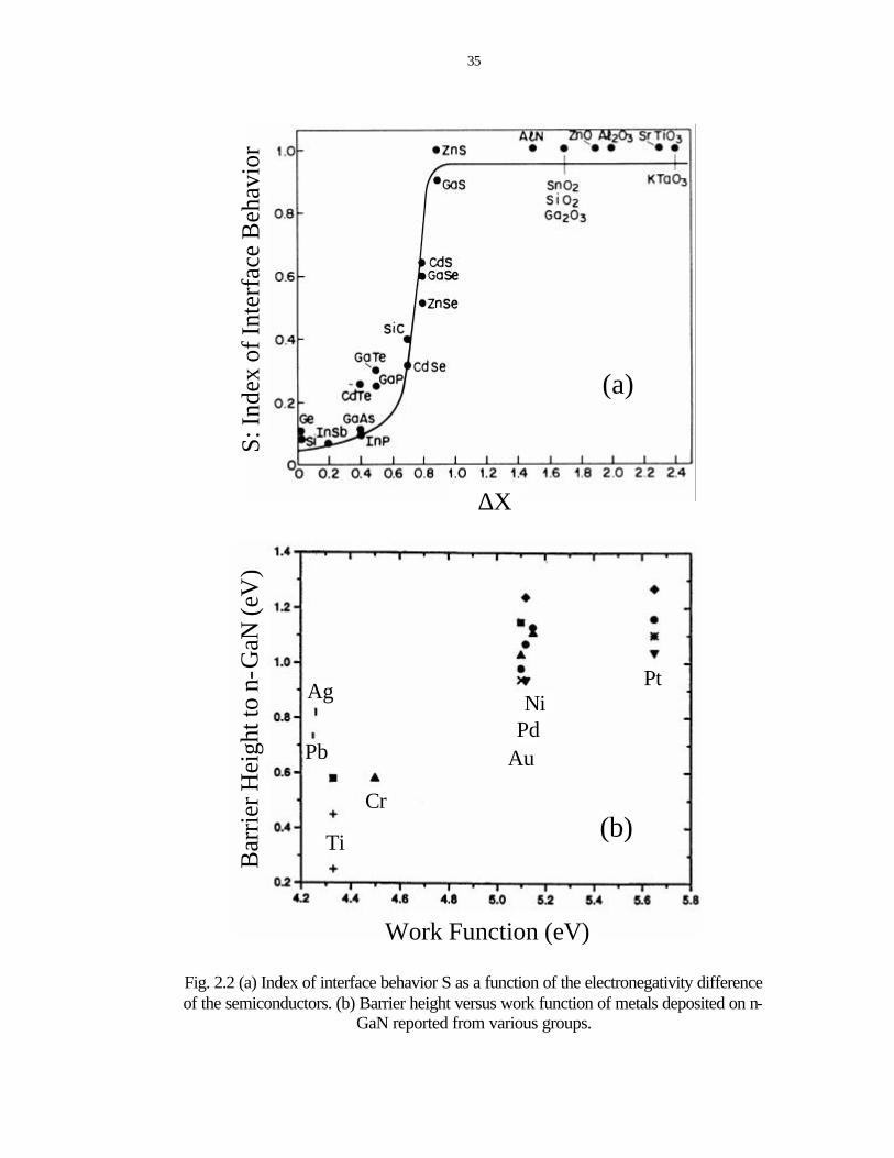
In a simple model for all semiconductors, the Schottky barrier height qφb can be
expressed as:75
qφb = q(Sχm + φ0) (2.5)
where χm is metal electronegativity, φ0 represents the contribution of surface states of
semiconductors, and interface index S=m
b
ddχφ
, is found to be a function of the
electronegativity difference ∆χ between cation and anion of compound semiconductor, as
shown in Fig. 2.2 (a). Note a sharp transition around ∆χ=1. For ionic semiconductors,
∆χ>1, the index S approaches 1, and φb is strongly dependent of the metal
electronegativity (or work function). On the other hand, for covalent semiconductors with
∆χ<1, S is small, φb is affected by high density surface states from dangling bonds and
only weakly depends on metal work function. GaN has an electronegativity difference of
1.4 (Ga: 1.6, N: 3.0), which would predict the Schottky barrier heights depend on metal
work function, and are given by eq. 2.3 and eq. 2.4 for metal on n-type and p-type

34
material respectively. A summary of reported Schottky barrier heights of a variety of
elemental metals on n-GaN is shown in Fig. 2.2 (b).54 It is clear that the barrier height
indeed varies with the metal work function within experimental scattering.
The current transport in metal-semiconductor contacts is mainly due to majority
carrier, in contrast to p-n junctions. Two major processes under forward bias are (1)
transport of electrons from the semiconductor over the potential barrier into the metal; (2)
quantum-mechanical tunneling of electrons through the barrier. In addition, we may have
recombination current in the space-charge region and leakage current at the contact
periphery. The transport of electrons over the potential barrier is often the dominant
process for Schottky diodes on moderately doped semiconductors. It can be adequately
described by thermionic emission theory for high mobility semiconductor (for low
mobility materials, the diffusion theory is also applicable), and the electric current density
over the barrier has the following expression:
J JqVkT
A TqkT
qVkTs
b= − = − −[exp( ) ] exp( )[exp( ) ]**1 12 φ (2.6)
where Js is the saturation current density, A** is the effective Richardson constant. In
practical device, the barrier height dependent on bias voltage, and the current-voltage
characteristics is more accurately described by:
J A TqkT
qVnkT
b= − −** exp( )[exp( ) ]2 1φ
(2.7)
Factor n is called the ideality factor. The barrier height and ideality factor can be obtained
from the forward J-V characteristics (for V>3kT/q):
35
Fig. 2.2 (a) Index of interface behavior S as a function of the electronegativity difference of the semiconductors. (b) Barrier height versus work function of metals deposited on n-
GaN reported from various groups.
(a)
(b)
PtNi
PdAu
Cr
Ti
Ag
Pb
∆X
S: In
dex
of In
terf
ace
Beh
avio
r
Work Function (eV)
Bar
rier
Hei
ght t
o n-
GaN
(eV
)

36
nqkT
VJ
=∂
∂ ln (2.8)
)ln(2**
sb J
TAq
kT=φ (2.9)
For a heavily doped semiconductor or for operation at low temperatures, the
tunneling current may become the dominant transport process. The tunneling current has
an expression:
)2
exp(~*
D
sbt N
mJ
εφh
(2.10)
where εs is permittivity of semiconductor, m* is effective mass of carrier, ND is carrier
concentration. It indicates the current will increase exponentially with ND0.5.
2.3.2 Ohmic Contact
It is imperative that a semiconductor device be connected to the outside world with
no adverse change to its current-voltage characteristics. This can be accomplished
through ideal ohmic contacts to the semiconductor. An ohmic contact is defined as a
metal/semiconductor contact that has negligible contact resistance relative to the bulk or
spreading resistance of the semiconductor. A satisfactory ohmic contact can supply the
required current with a voltage drop that is sufficiently small compared with the drop
across the active region of the devices. One important figure of merit for ohmic contact is
specific contact resistance rc, which is defined as:
rc = ∂∂
JV V
=
−
0
1
(2.11)

37
For contact with lower doping concentration, at relatively high temperature,
conduction across the M/S interface is dominated by thermionic-emission over the
potential barrier, as given in eq. 2.6. Therefore,
rc )exp(** kTq
TqAk bφ= (2.12)
It is obvious that low φb should be used for small rc. Ideally a metal with a lower work
function than an n-type semiconductor or higher work function than a p-type
semiconductor should be used for ohmic contact to this semiconductor. Unfortunately,
very few practical material systems satisfy this condition, and metals usually form
Schottky barriers at semiconductor interface. A practical way to obtain a low resistance
ohmic contact is to create a highly doped region near the surface by ion implantation, or
increase the doping by alloying the contacts. In this case, the depletion layer cause by the
Schottky barrier becomes very thin, and current transport through the barrier is enhanced
by tunneling. The contact resistance can be obtained from eq. 2.10,
rc ~ )2
exp(*
D
bs
N
m
h
φε (2.13)
Note that rc depends strongly on ND. Under intermediate conditions, thermionic field
emission is important, where there is enough kinetic energy for the carrier to be excited to
an energy level at which the potential barrier is thin enough for tunneling to occur.
Typical ohmic conduction is usually related to a large tunneling component.
The resistance of ideal planar contacts may be found using a transmission-line
method (TLM). This technique is based on the assumption that specific contact resistance
is determined by either the metal-semiconductor interface or by the interface between the
alloyed and nonalloyed portions of the active layer, and that the semiconductor resistivity
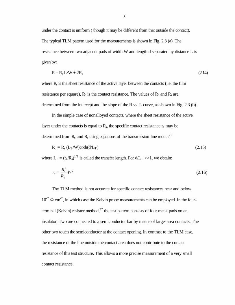
38
under the contact is uniform ( though it may be different from that outside the contact).
The typical TLM pattern used for the measurements is shown in Fig. 2.3 (a). The
resistance between two adjacent pads of width W and length d separated by distance L is
given by:
R = Rs L/W + 2Rc (2.14)
where Rs is the sheet resistance of the active layer between the contacts (i.e. the film
resistance per square), Rc is the contact resistance. The values of Rc and Rs are
determined from the intercept and the slope of the R vs. L curve, as shown in Fig. 2.3 (b).
In the simple case of nonalloyed contacts, where the sheet resistance of the active
layer under the contacts is equal to Rs, the specific contact resistance rc may be
determined from Rc and Rs using equations of the transmission-line model:76
Rc = Rs (LT/W)coth(d/LT) (2.15)
where LT = (rc/Rs)1/2 is called the transfer length. For d/LT >>1, we obtain:
22
WRR
rs
cc = (2.16)
The TLM method is not accurate for specific contact resistances near and below
10-7 Ω⋅cm-2, in which case the Kelvin probe measurements can be employed. In the four-
terminal (Kelvin) resistor method,77 the test pattern consists of four metal pads on an
insulator. Two are connected to a semiconductor bar by means of large-area contacts. The
other two touch the semiconductor at the contact opening. In contrast to the TLM case,
the resistance of the line outside the contact area does not contribute to the contact
resistance of this test structure. This allows a more precise measurement of a very small
contact resistance.

39
Fig. 2.3 Determination of contact and sheet resistance using the TLM measurements: (a) TLM pattern (b) resistance between the contact pads (width W) vs. distance between the
contacts.
Substrate
Active layer
L1 L2 L3
Distance L
Res
ista
nce
R
L1 L2 L3
Slope=RS/W
2Rc
(a)
(b)

40
It is difficult to make ohmic contacts on wide-bandgap semiconductors, such as
GaN (εg=3.4 eV, χ=4.1 eV) and SiC. Generally the doping concentration is relatively low
due to the high ionization level of typical dopants. A metal does not have high enough
work function to yield a low barrier on p-type material (qφm <5 eV for most metals). In
addition, the tendency to lose N during thermal processing which would contribute to n-
type conductivity makes the achievement of low-resistance ohmic contacts on p-GaN
particularly challenging. Other techniques for making an ohmic contact should be
explored, involving the establishment of a heavily doped surface layer by interface
reaction, alloys regrowth, or deposition of strained-layer superlattics and graded materials
to eliminate the barrier over the thickness of the contact layer.
2.4 Dry Etching
Wet chemical etching enjoys many advantages for device fabrication, including
simplicity, high selectivity, high throughput, low cost and low damage to the wafer.
However, its isotropic nature, which results in roughly equal removal of material in all
directions, makes it incapable of patterning submicron features. Dry etching, which
provides higher resolution potential by overcoming the problem of isotropy, has become
a favorable etching technique for VLSI/ULSI technology. In addition, it offers
advantages such as superior uniformity and compatibility with multichamber processing.
Especially for III-V nitrides, due to the lack of efficient wet etch recipes, dry etching has
become the dominant patterning technique.
Dry plasma etching proceeds by either physical sputtering, chemical reaction, or a
combination of the two often referred to as ion-assisted plasma etching. Physical

41
sputtering is dominated by the acceleration of energetic ions formed in the plasma to the
substrate surface at relatively high energies, typically >200 eV. Due to the transfer of
energy and momentum to the substrate, material is ejected from the surface. This
sputtering mechanism tends to yield anisotropic profiles. However it can result in rough
surface morphology, trenching, poor selectivity and nonstoichiometric surfaces thus
minimizing device performance. The etching rates are sensitive to the magnitude of
bonding force and structure of the surface, and typically quite slow.
Chemically dominated etch mechanisms rely on the formation of reactive species in
the plasma which adsorb to the surface, form volatile etch products, and then desorb from
the surface. Since ion energies are relatively low, etch rates in the vertical and lateral
direction are often similar thus results in isotropic etch profiles and loss of critical
dimensions. However, good etch rate and selectivity can be achieved, and the plasma-
induced damage is minimized.
The chemical etching is rapid, but isotropic, whereas the physical etching is slow,
but anisotropic. Provided the chemical and physical components of the etch mechanism
are balanced, high-resolution features and high etch rates with minimal damage can be
realized. This ion-assisted plasma etching is the typical mechanism of most current dry
etching techniques.
Reactive ion etching (RIE) is one of the dry etching techniques in common usage,
which utilizes both the chemical and physical components of an etch mechanism. RIE
plasmas are typically generated by applying radio frequency (rf) power of 13.56 MHz
between two parallel electrodes in a reactive gas (see Fig. 2.4(top)). The sample to be
etched is placed on the powered electrode where a potential is induced, and is subject to

42
the ion bombardment and impingement of neutral gas atoms and molecules from the
plasma. Ion energies, defined as they cross the plasma sheath, are typically a few hundred
eV. Etching is typically performed at low pressures, ranging from a few mTorr up to 200
mTorr, which promotes anisotropic etching due to increased mean free paths and reduced
collisional scattering of ions during acceleration in the sheath. RIE is by far the most
popular dry etching technique used for conventional III-V materials, and takes advantage
of the fact that there is a synergism between the physical and chemical etching
mechanisms. The observed etch rates are faster than the sum of these two components.
This is usually ascribed to the fact that the volatile etch products formed by
chemisorption of active species from the plasma onto the semiconductor surface are
quickly removed by physical sputtering, exposing a fresh layer of the material. Good
results for the III-V nitrides have been obtained in chlorine-based plasma under high ion
energy conditions where the III-N bond breaking and the sputter desorption of etch
products are most efficient. Unfortunately, the high energy plasma may induce significant
damage and degrade both electrical and optical device performances. Lowering the ion
energy and increasing the chemical activity in the plasma often results in much slower
etch rates and less anisotropic profiles. It is necessary to pursue alternative etch platforms
which combine high quality etch characteristics with low damage for III-V nitrides.
The use of high-density plasma etch systems, such as inductively coupled plasma
(ICP)61 and electron cyclotron resonance (ECR)63, has resulted in improved etch
characteristics for the III-V nitrides as compared to RIE. This observation is attributed to
plasma densities which are 2-4 orders of magnitude higher than RIE thus improving the
III-N bond breaking efficiency and the sputter desorption of etch products for the surface.

43
Additionally, since ion energy and ion density can be more effectively decoupled, plasma
induced damage is more readily controlled. Fig. 2.4 (bottom) shows a schematic diagram
of a typical ICP etch system. High density ICP plasmas are formed in a dielectric vessel
encircled by an inductive coil into which rf power is applied. The alternating electric field
between the coils induces a strong alternating magnetic field trapping electrons in the
center of the chamber and generating plasmas with uniform density and energy
distribution. By keeping ion and electron energy low, we can obtain low damage etching
while maintaining fast etch rates. Anisotropy is achieved by superimposing a rf bias on
the sample. Generally, etch characteristics are dependent upon plasma parameters
including ion energy (controlled by rf chuck power), plasma density (controlled by ICP
source power), and operation pressure ( the change in collisional frequency can result in
changes in both ion energy and plasma density). Compared to ECR, where high-density
plasmas are formed through magnetic confinement of electrons in the source region, ICP
etching is generally believed to have several advantages including easier scale-up for
production, improved plasma uniformity and lower cost of operation.
It is important to choose appropriate plasma chemistries to achieve good etch rates,
anisotropy, selectivity, and morphology. The fragmentation pattern and gas-phase
kinetics associated with the source gas can have a significant effect on the concentration
of a reactive neutrals and ions generated in the plasma thus affecting the etch
characteristics. Secondary gases such as Ar, N2, H2, or SF6 can be added to change the
chemical : physical ratio of the etch mechanism, and therefore achieve better profiles or
higher rates. Another important factor affecting the etch characteristics is the volatility of
the etch products formed. Table 2.1 shows the boiling points of possible etch products for
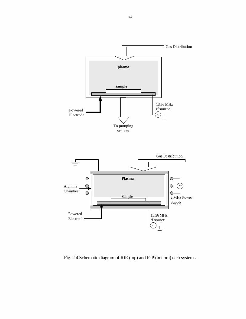
44
Fig. 2.4 Schematic diagram of RIE (top) and ICP (bottom) etch systems.
Powered Electrode
plasma
Gas Distribution
sample
To pumping system
~
13.56 MHz rf source
~
13.56 MHz rf source
Gas Distribution
Alumina Chamber
Powered Electrode
Plasma
Sample
~
2 MHz Power Supply

45
Table 2.1 Boiling points for possible etch products of III-V nitrides etched in halogen- or CH4/H2-based plasmas.
Etch products Boiling point (oC)
AlCl3 183 AlF3 Na
AlI3 360
AlBr3 263
(CH3)3Al 126
GaCl3 201
GaF3 1000
GaI3 Sublimes 345
GaBr3 279
(CH3)3Ga 55.7
InCl3 600
InF3 >1200
InI3 Na
InBr3 Sublimes
(CH3)3In 134
NCl3 <71
NF3 -129
NBr3 Na
NI3 Explodes
NH3 -33
N2 -196
(CH3)3N -33
III-V nitrides exposed to halogen- and hydrocarbon-based plasmas. For halogen-based
plasmas, etch rates are often limited by the volatility of the group III halogen etch
products. Cl-based plasmas typically yield fast rates with anisotropic, smooth etch
profiles for Ga- and Al-containing films. In a contrast, etch rates for In-containing

46
materials in room temperature Cl-based plasmas tend to be slow with rough surface
morphology and overcut profiles due to the low volatility of InCl3 and preferential loss of
the group V etch products. Significant better room temperature etch results are obtained
in CH4/H2-based plasma due to the formation of more volatile (CH3)3In.63 Based only on
Table 2.1, high etch rates can also be expected for Ga-containing films in CH4/H2-based
plasmas since the (CH3)3Ga has a much lower boiling point than GaCl3. However, in
practice very slow rates are observed, which demonstrates the complexity of the etch
process where redeposition, polymer formation, and gas-phase kinetics can influence the
results.

48
CHAPTER 3 ULTRA-HIGH TEMPERATURE ACTIVATION OF IMPLANT DOPING IN GaN
3.1 Introduction
Ion implantation is an enabling technology for selected-area doping or isolation of
advanced semiconductor devices. Implantation of donors at high doses can be used to
decrease source and drain access resistance in FETs, at lower doses to create channel
regions for FETs, while sequential implantation of both acceptors and donors may be
used to fabricate p-n junctions. In addition, ion implantation is a suitable technological
tool to explore doping, compensation effects, and redistribution properties of the potential
dopant species.
The first work on implantation in GaN was performed by Pankove and co-workers
in the earlier 1970s.78 They reported primarily on the photoluminescence properties of a
large array of implanted impurity in GaN. The work was successful in identifying Mg as
the shallowest acceptor found to date for GaN. In 1995, Pearton et al.30 achieved
electrically active n- and p-type dopants in GaN by implantation of Si and Mg
respectively. Subsequently, implanted O was shown to also be a donor and implanted Ca
an acceptor in GaN.31 Two different GaN based device structures have been
demonstrated using implant doping, namely a junction field effect transistor46 and a
planar homojunction LED.79
Tan et al.80 have observed that low dose ( ≤ 5 ×1014 cm-2) implants in GaN anneal
poorly up to 1100 °C, leaving a coarse network of extended defects, while high dose ( ≥
48
2×1015 cm-2) implants may lead to amorphization. Amorphous layers recrystallize in the
range 800-1000 °C to form defective polycrystalline material. Quite good activation
efficiencies have been obtained for n-type implanted dopants in spite of high residual
damage.30,51 It is also clear that annealing temperatures above 1300 °C are desirable for
optimal electrical properties in the implanted layers.51 At these temperatures, the
equilibrium N2 pressure over GaN is very high, thus surface protection is necessary to
prevent dissociation of the GaN. The most effective and convenient approach is use of an
AlN encapsulant that can be removed selectively in KOH after annealing. This technique
is attractive for processing of GaN devices in a conventional fabrication-line
environment, without the need for specialized high-pressure furnaces.
In this chapter we first introduced a novel rapid thermal processing (RTP) up to
1500 oC to the GaN material system, used in conjunction with AlN cap layers. The high
temperature activation characteristics of implanted Si and Group VI donors were then
examined. The activation of Mg, Be and C for p-type doping has also been investigated,
along with the redistribution of all these species in GaN. Finally the effectiveness of the
new RTP for removing lattice damage in implanted GaN was studied by TEM.
3.2 High Temperature Annealing and AlN Encapsulation
In the development of advanced electronic devices, the technology of rapid thermal
processing plays a critical role at numerous points such as implant activation of dopant
species, implantation-induced damage removal, alloying of ohmic contacts, maximization
of sheet resistance in implant isolation regions, etc. The existing commercial RTP
equipment typically relies on a series of tungsten-halogen lamps as heat sources to

49
rapidly heat up the semiconductor wafers, and only has modest temperature capacity
(<1100 oC), primarily because of the point-like nature of the sources and large thermal
mass of the systems. Recent interest in developing wide bandgap compound
semiconductors such as SiC and GaN has pushed the processing temperature
requirements to much higher values (up to 1500 oC).
To meet thus an urgent need, MHI Inc., in collaboration with the University of
Florida, has recently developed a unique high temperature RTP unit called ZapperTM,
which can achieve such high processing temperatures. To realize higher temperature
capacity, novel molybdenum intermetallic composite heat sources have been employed,
which may be used in air at temperatures up to 1900 oC. These heaters have high
emissivity (up to 0.9) and allow heat-up time of the order of seconds and heat fluxes up to
100 W/cm2. The ZapperTM unit relies on wafer movement (in/out of the furnace
horizontally) to achieve rapid ramp-up or ramp-down rates (~50 °C /s and 25 °C /s
respectively). Excellent temperature uniformity (≤ ±4 °C over a 9×6" area at 1500 °C),
good reproducibility can be obtained. Fig. 3.1 shows the typical temperature-time profiles
for an annealing cycle at 1400 oC and 1500 °C.
To examine the thermal stability of the nitrides, a variety of undoped GaN and AlN
wafers were sealed in quartz ampoules under N2 gas, and annealed in Zapper TM unit at
different time-temperature combinations. The GaN layers ~ 3 µm thick were grown at
~1050 oC by MOCVD using trimethylgallium and ammonia. Growth was preceded by
low-temperature deposition of thin (~200 Å) AlN buffers on Al2O3 substrates. Some AlN
layers were deposited by reactive sputtering of pure AlN targets in 300 mTorr of 20%
N2Ar at 400 oC. The others were grown by metal organic molecular beam epitaxy

50
Fig. 3.1 Time-temperature profiles for ZapperTM RTP annealing at 1400 oC and 1500 oC.

51
(MOMBE) at 750 oC using dimethlamine alane and plasma dissociated nitrogen.81 The
N2 pressure in the quartz ampoules was ~15 psi. This negative pressure was necessary to
prevent blowout of the ampoule at elevated annealing temperatures. The samples were
then annealed at 1100 oC – 1500 oC for a dwell time of ~10 s.
Fig. 3.2(top) shows scanning electron microscopy (SEM) micrographs of the GaN
surfaces annealed at 1200 -1500 °C. The 1200 °C annealing does not degrade the surface,
and the sample retains the same appearance as the as-grown material. After 1300 °C
annealing, there is a high density (~108 cm-2) of small hexagonal pits due to incongruent
evaporation from the surface. The 1400 °C treatment produces complete dissociation of
the GaN, and only the underlying AlN buffer survives. Annealing at 1500 °C also causes
loss of this thin buffer layer, and a smooth exposed Al2O3 substrate is evident. The
corresponding root-mean-square (RMS) surface roughness of these samples measured by
atomic force microscopy (AFM) scans is shown in Fig 3.2 (bottom).
In sharp contrast, both the sputtered and MOMBE-grown AlN were found to
survive annealing up to 1400-1500 °C. However, for the sputtered materials, we often
observed localized failure of the film (Fig 3.3(top)), possibly due to residual gas (Ar or
H2) agglomeration to form bubbles. The surface roughness tends to go through a
maximum at ~ 1300 oC, partially due to some initial localized bubbling, followed by the
film densification at temperatures ≥ 1400 oC, as shown in Fig. 3.3 (bottom). The film
retains its integrity even at 1450 oC, and appears to be more thermally stable than the AlN
buffer layer under the GaN (Fig. 3.2). This can be attributed to the fact that the AlN was
deposited at higher temperature (400 oC compared to 300 oC for the buffer layers) and

52
1200 oC 1300 oC
1500 oC1400 oC
Fig. 3.2 SEM micrographs (top) and RMS roughness (bottom) of GaN surfaces annealed at 1200 -1500 oC.
Annealing Temperature (oC)
1100 1200 1300 1400 1500 1600
RM
S R
ough
ness
(nm
)
0
4
8
12
16
GaN

53
Fig. 3.3 SEM micrographs (top) and RMS roughness (bottom) of AlN surfaces annealed at 1150 -1450 oC.
1150 oC 1250 oC
1350 oC 1450 oC
Annealing Temperature (oC)
1100 1200 1300 1400 1500
RM
S R
ou
gh
ne
ss (
nm
)
10
100
AlN

54
therefore is denser and contains less residual entrapped gas. For the MOMBE grown
films, the localized material failure was basically absent.
There is clear evidence from previous work that temperatures above 1300 oC are
required to completely remove implantation damage and to achieve the optimal dopant
activation in GaN. However, the above results show that a premium is placed on
prevention of loss of nitrogen or even surface dissociation under those conditions. AlN
encapsulation can preserve the surface quality to 1500 oC, which is quite promising for
the high temperature activation processes.
3.3 N-type Implant Doping
Nominally undoped (n~5×1016 cm-3) GaN was grown on c-plane Al2O3 substrates
MOCVD. Samples were implanted at room temperature in a non-channeling direction
with 150 keV 28Si+ ions at a dose of 5×1015 cm-2, 200 keV 32S+ and 600 keV 128Te+ ions at
doses of 5×1014 cm-2 for n-type doping. The Si implant is a standard condition for
producing very high n-type doped regions in GaN when combined with high temperature
RTA. All samples were capped with ~1000 Å reactively sputtered AlN, and annealed at
1200-1500 °C under a N2 ambient in the ZapperTM furnace for a dwell time of ~10 secs.
Following annealing, the AlN was removed in aqueous KOH at ~80 °C, and the samples
were characterized. For measurement of the electrical properties, HgIn ohmic contacts
were alloyed to the corners of 3×3 mm2 sections, and Hall effect data was recorded at 25
oC in all cases.
Fig. 3.4(a) shows an Arrhenius plot of sheet carrier concentration in Si+ implanted
material. As a comparison, the electrical results for the unencapsulated samples are also
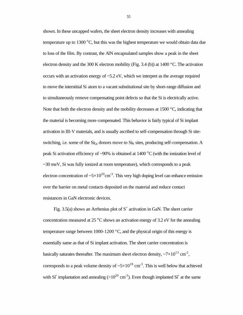
55
shown. In these uncapped wafers, the sheet electron density increases with annealing
temperature up to 1300 oC, but this was the highest temperature we would obtain data due
to loss of the film. By contrast, the AlN encapsulated samples show a peak in the sheet
electron density and the 300 K electron mobility (Fig. 3.4 (b)) at 1400 °C. The activation
occurs with an activation energy of ~5.2 eV, which we interpret as the average required
to move the interstitial Si atom to a vacant substitutional site by short-range diffusion and
to simultaneously remove compensating point defects so that the Si is electrically active.
Note that both the electron density and the mobility decreases at 1500 °C, indicating that
the material is becoming more compensated. This behavior is fairly typical of Si implant
activation in III-V materials, and is usually ascribed to self-compensation through Si site-
switching, i.e. some of the SiGa donors move to SiN sites, producing self-compensation. A
peak Si activation efficiency of ~90% is obtained at 1400 oC (with the ionization level of
~30 meV, Si was fully ionized at room temperature), which corresponds to a peak
electron concentration of ~5×1020cm-3. This very high doping level can enhance emission
over the barrier on metal contacts deposited on the material and reduce contact
resistances in GaN electronic devices.
Fig. 3.5(a) shows an Arrhenius plot of S+ activation in GaN. The sheet carrier
concentration measured at 25 oC shows an activation energy of 3.2 eV for the annealing
temperature range between 1000-1200 °C, and the physical origin of this energy is
essentially same as that of Si implant activation. The sheet carrier concentration is
basically saturates thereafter. The maximum sheet electron density, ~7×1013 cm-2,
corresponds to a peak volume density of ~5×1018 cm-3. This is well below that achieved
with Si+ implantation and annealing (>1020 cm-3). Even though implanted Si+ at the same

56
Fig. 3.4 Sheet carrier concentration (a) and electron mobility (b) in Si-implanted GaN after uncapped and AlN-capped annealing.
AlN capped
unencapsulated
1000/T (1/K)
0.5 0.6 0.7 0.8 0.9
She
et C
arrie
r C
once
ntra
tion
(cm
-2)
1012
1013
1014
1015
1016
unencapsulatedAlN capped
E a = 5 . 2 e V
S i+ → ΓαΝ
150 κες 5 ξ1015 c m
-2
1 0 s e c a n n e a l
(a)
Annealing Temperature (oC)
1000 1200 1400 1600
Car
rier
Mob
ility
(cm
-2/V
. s)
0
20
40
60
unencapsulatedAlN capped
(b)

57
dose showed evidence of site-switching and self-compensation, it still produces a higher
peak doping level than the non-amphoteric donor S, which is only slightly heavier(32S vs.
28Si). From temperature-dependant Hall measurements, we find a S+ donor ionization
level of 48±10 meV, so that the donors are fully ionized at room temperature.
Similar data is shown in Fig. 3.5 (b) for Te+ implantation. The activation starts
around the same temperature as for S, but much lower sheet electron densities are
obtained, the activation energy is significantly lower (1.5 eV) and the carrier
concentration does not saturate, even at 1400 °C. It is likely that because of the much
greater atomic weight of 128Te, even higher annealing temperatures would be required to
remove all its associated lattice damage, and that the activation characteristics are still
being dominated by this defect removal process. Residual lattice damage from the
implantation is electrically active in all III-V semiconductors, producing either high
resistance behaviors (GaAs) or residual n-type conductivity (InP, GaN). The only data
available on group VI doping in epitaxial material is from Se-doped MOCVD material,
where maximum electron concentrations of 2×10¹⁸ – 6×1019 cm-3 were achieved.82 These
are also below the values reported for Si-doping, and suggests the group VI donors do not
have any advantage over Si for creation of n-type conductivity in GaN. From limited
temperature-dependent Hall data, we estimate the Te ionization level to be 50±20 meV.
3.4 P-type Implant Doping
Similar GaN samples were implanted with 80 keV 9Be+, 80 keV 12C+, or 150 keV
24Mg+ at doses of 3-5×1014 cm-2 for p-type doping. Post-implant annealing was

58
Fig. 3.5 Arrhenius plots of sheet electron density in S (a) and Te (b) implanted GaN as a
function of annealing temperature.
1000/T (K-1)
0.55 0.60 0.65 0.70 0.75 0.80 0.85 0.90
She
et C
arrie
r C
once
ntra
tion
(cm
-2)
1012
1013
1014
S+ → GaN5 x 1014 cm -2
Ea,S = 3.2 eV
(a)
1000/T (K-1)
0.55 0.60 0.65 0.70 0.75 0.80 0.85 0.90
She
et C
arrie
r C
once
ntra
tion
(cm
-2)
1012
1013
1014
Te+ → GaN5 x 1014 cm-2
Ea, Te = 1.5 eV
(b)

59
performed at 1000-1400 °C under a N2 ambient in the ZapperTM furnace for ~10 secs in
conjunction with ~1000 Å AlN encapsulation.
The effects of the annealing temperature on the sheet carrier concentrations in Mg+
and C+ implanted GaN are shown in Fig. 3.6. There are two important features of the
data: first, we did not achieve p-type conductivity with carbon, and second only ~1% of
the Mg produces a hole at 25 °C. Carbon has been predicted previously to have a strong
self-compensation effect,83 and it has been found to produce p-type conductivity only in
metal organic molecular beam epitaxy where its incorporation on a N-site is favorable.84
Based on an ionization level of ~170 meV, the hole density in Mg-doped GaN would be
calculated to be ~10% of the Mg acceptor concentration when measured at 25 °C. In our
case we see an order of magnitude less holes than predicted. This should be related to the
existing n-type carrier background in the material and perhaps to residual lattice damage
which is also n-type in GaN. At the highest annealing temperature (1400 °C), the hole
density falls, which could be due to Mg coming out of the solution or to the creation of
further compensating defects in the GaN. The results of Be implant are similar with those
of C implant, i.e. remaining n-type after annealing, probably also due to a strong
compensation effect. This data indicates that ion implantation is not so efficient for
creating p-type conductivity in state-of-the-art GaN as epitaxial growth doping.
3.5 Dopant Redistribution
Fig. 3.7 shows the calculated, as-implanted Si atomic profile, and the secondary ion
mass spectroscopy (SIMS) profiles of as-implanted and 1400 °C annealed samples. The
calculated profile does not produce a good match to the experimental profile, and some

60
Fig. 3.6 Sheet carrier concentrations in Mg+ and C+ implanted GaN as a function of annealing temperature.
work will need to be done to obtain better stopping power data for the ions in GaN. There
is little redistribution of the Si at 1400 oC, with the diffusivity ≤ 10-13 cm2 ⋅sec-1 calculated
from the change in width at half-maximum. This result emphasizes the extremely stable
nature of Si dopant in GaN even at very high processing temperatures.
Fig. 3.8 (top) shows SIMS profiles before and after 1450 °C annealing of implanted
S in GaN. There is clearly no motion of the sulfur under these conditions and the profiles
Annealing Temperature (o C)
900 1100 1300 1500
She
et C
arri
er C
once
ntra
tion
(cm
-2)
2x10¹²
4x10¹²
6x10¹²
8x10¹²
Mg p-typeMg n-type
C n-type
Mg+, C+ → GaN 5x1014 cm-2

61
Fig. 3.7 Calculated and experimentally measured (by SIMS) profiles of implanted Si (150 keV, 5×1015 cm-2) in GaN.
Depth (µµm)
0.0 0.4 0.8 1.2 1.6
Si C
once
ntra
tion
(cm
-3)
1017
1018
1019
1020
1021
calculated profileas-implanted1400 oC, 10 s
Si+ in GaN 150 keV 5x1015 cm-2

62
are essentially coincident. Wilson85 reported some redistribution of implanted S after
annealing at 700-1000 °C in relatively thin layers of GaN, which might have been
influenced by the high crystalline defect density in the material. The samples in the
present experiment are much thicker and the extended defect density will be
correspondingly lower in the implanted region (~5×108 cm-2 compared to ~1010 cm-2 in
the thin samples). The other group VI donors, Se and Te, have low diffusion coefficients
in all compound semiconductors (for example DSe=5×10-15 cm2⋅sec-1 at 850 °C in
GaAs),64 and we find a similar result for these species implanted into GaN, as shown in
Fig. 3.8 (bottom). Given the resolution of SIMS measurement (~200 Å under these
conditions), we can obtain the diffusivity at this temperature ≤ 2×10-13 cm2 ⋅sec-1using a
simple 2 Dt estimation.
Fig. 3.9 (top) shows SIMS profile of implanted Mg in GaN, both before and after
annealing at 1450 °C. Again, within the resolution of SIMS, there is no motion of the
Mg. This is in sharp contrast to its behavior in GaAs,86,87 where the rapid diffusion of the
Ga-site acceptors during annealing can only be suppressed by co-implanting a group V
element to create a sufficient number of vacant sites for the initially interstitial acceptor
ions to occupy upon annealing. This reduces the effective diffusivity of the acceptor and
increases its electrical activation. In addition, implanted Mg in GaAs often displays out-
diffusion toward the surface (in most case up, rather than down, the concentration
gradient), leading to loss of dopant into the annealing cap.88 This has been suggested to
be due to non-equilibrium levels of Ga interstitials created by the implantation process.
This mechanism is clearly absent for implanted Mg in GaN.

63
Fig. 3.8 SIMS profiles of S+ (top) and Te+ (bottom) implanted GaN before and after annealing at 1450 oC (the profiles are essentially coincident).
S+→GaN200 keV, 5×1014 cm-2
as-implanted and annealed at 1450 oC
GaN
GaN
Te+→GaN600 keV, 3×1014 cm-2
as-implanted and annealed at 1450 oC
1016
1018
1020
1016
1018
1020
1014
102
104
106
100
0 0.2 0.4 0.6
Depth (µm)
0 0.6 1.2 1.8
Depth (µm)
Ato
m D
ensi
ty (c
m-3
)A
tom
Den
sity
(cm
-3)
Seco
ndar
y Io
n In
tens
ity (c
ts/s
ec)

64
Carbon is typically a very slow diffuser in all III-V compounds, since it strongly
prefers substitutional lattice sites.88,89 In general carbon occupies both Ga and N sites in
GaN, and the material containing high concentrations of carbon is found to be self-
compensated. Fig. 3.9 (bottom) shows that it is also an extremely slow diffuser when
implanted into GaN, with Deff ≤2×10-13 cm⋅sec-1 at 1400 °C.
Fig. 3.10 shows a series of profiles for 9Be before and after annealing up to 1200
°C. Note that there is an initial broadening of the profile at 900 °C, corresponding to an
effective diffusivity of ~5×10-13 cm2⋅sec-1 at this temperature. However there is no
subsequent redistribution at temperatures up to 1200 °C. It appears that in GaN, the
interstitial Be undergoes a type of transient-enhanced diffusion until these excess point
defects are removed by annealing, at which stage the Be is basically immobile. Implanted
Be shows several types of anomalous diffusion in GaAs, including up-hill diffusion and
movement in the tail of the profile, in addition to normal concentration-dependent
diffusion,90 which also result from the non-equilibrium concentrations of point defects
created by the nuclear stopping process of the implanted ions.
The above results show that most of the common acceptor and donor species
implanted into GaN, with the exception of Be, are extremely slow diffusers at high
temperatures. This bodes well for the fabrication of GaN-based power devices such as
thyristors and insulated gate bipolar transistors that will require creation of doped well or
source/drain regions by implantation. The low diffusivities of implanted dopants in GaN
means that junction placement should be quite precise and there will be less problems
with lateral diffusion of the source/drain regions towards the gate. In addition, these
results also show the effectiveness of the AlN cap in protecting the GaN surface from
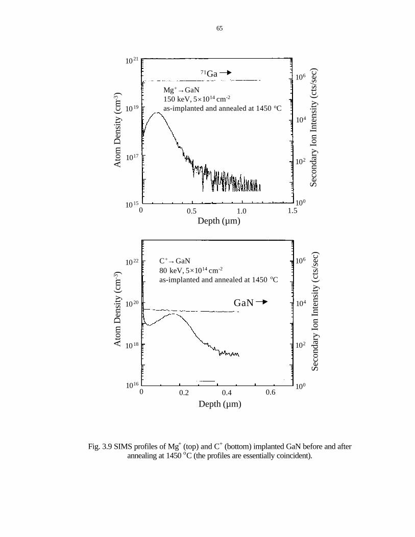
65
Fig. 3.9 SIMS profiles of Mg+ (top) and C+ (bottom) implanted GaN before and after annealing at 1450 oC (the profiles are essentially coincident).
1016
1018
1020
1017
1019
1021
1015
102
104
106
100
0 0.2 0.4 0.6
Depth (µm)
0 0.5 1.0 1.5Depth (µm)
Ato
m D
ensi
ty (c
m-3
)A
tom
Den
sity
(cm
-3)
Seco
ndar
y Io
n In
tens
ity (
cts/
sec)
Mg+→GaN150 keV, 5×1014 cm-2
as-implanted and annealed at 1450 oC
71Ga
102
104
106
100
Seco
ndar
y Io
n In
tens
ity (c
ts/s
ec)
C+→GaN80 keV, 5×1014 cm-2
as-implanted and annealed at 1450 oC
1022
GaN

66
Fig. 3.10 SIMS profiles of Be+ implanted GaN before and after annealing at different temperatures.
9Be+→GaN80 keV 5×1014 cm-2

67
dissociation, since if any of the surface was degraded during annealing, the implant
profiles would no longer overlap.
3.6 Residual Damage
Fig. 3.11 shows a plan view TEM and selected area electron diffraction pattern
from a Si-implanted sample (150 keV, 5×1015 cm-2) after annealing at 1100 °C for 10
secs. This is a high dose implant of the type used for making n+ ohmic contact regions,
and represents a worst-case scenario in terms of damage removal. It also allows
comparison to damage expected with other dopants such as S, Ca and Mg due to the
representative mass number of Si. The sample is still single-crystal as determined by the
diffraction pattern, but contains a high density of extended defects (~1010 cm-2). This is
consistent with past reports of high backscattering yields in implanted GaN annealed at
these conditions.66,91 We ascribe these defects to the formation of dislocation loops in the
incompletely repaired lattice.
By sharp contrast, annealing at 1400 °C for 10 secs brings a substantial reduction in
the implant-induced defects, as shown in Fig. 3.12. The sample is again single-crystal,
but the only contrast in the TEM plan view is due to the lower density (~109 cm-2) of
threading dislocations arising from lattice-mismatch in the heteroepitaxy. This appears to
correlate well with the fact that the highest electron mobility and carrier density in these
samples was observed for 1400 °C annealing. Clearly the ultra-high temperature
annealing is required to completely remove lattice damage in GaN implanted with high
doses. However it may not be needed for the material implanted with lower dose
(≤5×1013 cm-2) where the amount of damage created is correspondingly less.

68
Fig. 3.11 TEM plan view (a) and selected -area diffraction pattern from Si+-implanted GaN after 1100 oC, 10 s annealing.
Fig. 3.12 TEM plan view (a) and selected-area diffraction pattern from Si+-implanted
GaN after 1400 oC, 10 s annealing.

68
CHAPTER 4 HIGH RESISTANCE IMPLANT ISOLATION IN GaN
4.1 Introduction
Implant isolation has been widely used in compound semiconductor devices for
inter-device isolation such as in transistor circuits or to produce current channeling such
as in lasers. The implantation process can compensate the semiconductor layer either by a
damage or chemical mechanism, maintaining a planar device morphology without the
need for etched mesa isolation. For the former compensation, high resistivity is created
due to introduction of mid-gap, damage-related levels, which trap the free carriers in the
materials. This effect is stable only to the temperature at which the damage is annealed
out. For the latter case, the implanted species occupy the substitutional sites and create
chemically induced deep levels in the middle of the bandgap. The compensation is
thermally stable in the absence of outdiffusion or precipitation of the species. There is a
strong need for an understanding of the implant isolation process in GaN because of the
emerging applications for high temperature, high power electronics based on this material
and its alloys.
To date in the GaN materials system there has only been an examination of
damage-induced isolation. Binari et al.52 investigated H+ and He+ isolation of n-GaN,
with the material remaining compensated to over 850 oC with He+ and 400 oC with H+.
Subsequent work focused on N+ implantation into both n- and p-type GaN, producing
defect levels of 0.83 eV and 0.90 eV, respectively.30 The implantation damage was

70
annealed out at 850 oC in n-type and 950 oC in p-type material. Very effective isolation of
AlGaN heterostructure field effect transistor structures has been achieved with a
combined P+/He+ implantation leading to sheet resistances of ≥1012 Ω/ and an
activation energy of 0.71 eV for the resistivity.92 Some work has also been reported for
isolation of In-containing nitrides using O+, F+ or N+.53 Basically, the implantation in InN
and InGaN ternaries produced only one or two orders of magnitude increase in sheet
resistance after an optimum anneal. The relatively low sheet resistance (~104 Ω/)
achieved is not sufficient for inter-device isolation in electronic circuits.
To create chemically-induced isolation, it is necessary to implant impurities with
electronic levels in the GaN bandgap, and usually a minimum dose (dependent on the
doping level of the sample) is required. In other compound semiconductors, species such
as Fe, Cr, Ti and V have been employed, with other examples being O in AlGaAs (where
Al-O complexes are thought to form)93 and N in GaAs (C) (where C-N complexes are
thought to form).94
In this chapter multi-energy O+, Ti+, Fe+ or Cr+ were implanted into n- and p-type
GaN to create high resistivity. The annealing temperature dependence of the sample sheet
resistance was measured up to 900 oC. The defect levels in the materials of both types
were determined by temperature-dependent TLM measurements. The thermally stable,
electrically active concentration of deep states produced by these species was found to be
<7×1017 cm-3 in both conductivity types of GaN, with the sample resistivity approaching
its original, unimplanted value by ~900 oC in all cases. The defect levels created in the
implanted material are within 0.5 eV of either bandedge.

71
4.2 O-implantation for Selective Area Isolation
0.3 µm thick n (Si-doped) or p (Mg-doped) type GaN layers were grown on 1 µm
thick undoped GaN on (0001) sapphire substrates by rf plasma activated Molecular Beam
Epitaxy. The carrier concentration in the doped layers was 7×1017 cm-3 in each case.
Ohmic contacts were formed in a transmission line pattern (gap spacings of 2, 4, 8, 16
and 32 µm) by e-beam evaporation and lift-off of Ti/Au (n-type) and Ni/Au (p-type)
annealed at 800 oC and 700 oC, respectively, for 30 s under N2. The total metal thickness
was 4000 Å, so that these regions could act as implanted masks. A schematic of the
resultant structure is shown in Fig 4.1.
Fig. 4.1 Schematic of GaN structure for measurement of sheet resistance after ion implantation.
Ti/Au (Ni/Au for p-GaN) ~4000 Å
1 µm undoped GaN
Al2O3 substrate
0.3 µm n/p-GaN

72
The samples were then implanted at 25 oC using multiple-energy O+ ions at
different doses: 50 keV, 1×1014 cm-2; 100 keV, 2×1014 cm-2; 200 keV, 3×1014 cm-2. The
total dose was therefore 6×1014 cm-2. The sheet resistance was obtained from TLM
measurements for both the as-implanted sample and those annealed at increasing
temperatures to 900 oC. Measurement temperatures in the range of 25 oC-200 oC were
employed to determine the defect levels in the material.
In the case where the implanted species is chemically active in the GaN it is the ion
profiles that are the important feature, since it is the electrically active fraction of these
implanted species that determines the isolation behavior. In the case where the isolation
simply results from damage-related deep levels, then it is the profile of ion damage that is
important. Fig. 4.2 shows both the calculated ion profiles (top, from P-CODETM
simulations) and damage profiles (bottom, from Transport-of-Ions-in-Matter (TRIM)
simulations) for the multiple energy O+ implant scheme. Note that the defect density is
generally overstated in these calculations due to recombination of vacancies and
interstitials. In any case, the doses are below the amorphization threshold for GaN.
Fig. 4.3 (top) shows the evolution of the sheet resistance for O+ implanted n- and p-
type GaN with annealing temperature. For n-type sample, the as implanted sheet
resistance was 4×10⁹ Ω/, and gradually decreased over the entire annealing
temperature range. We do not believe this is a result of O-related shallow donor states
because these are not activated until annealing temperatures above 1100 oC.30 By
contrast, the trend in the sheet resistance in p-type GaN is typical of those observed with
damage-related isolation.64 The as-implanted resistance is 5 orders of magnitude higher

73
than that of the unimplanted material due to creation of deep traps that remove holes from
the valence

74
Fig. 4.2 Ion (top) and Damage (bottom) profiles for multiple energy O+ implant sequence into GaN.
Depth (Å)0 1000 2000 3000 4000
Ato
ms
(cm
-3)
1015
1016
1017
1018
1019
1020
O+→ GaN
1x1014 cm-2, 50 keV
2x1014 cm-2, 100 keV
3x1014 cm-2, 200 keV
Depth (Å)
0 1000 2000 3000 4000
Vac
ancy
Den
sity
(cm
-3)
1020
1021
1022
1023

75
band. Subsequent annealing tends to further increase the sheet resistance, by reducing
the probability for hopping conduction as the average distance between trap sites is
increased.95 Beyond particular annealing temperature (600 oC in this case) the trap
density begins to fall below the carrier concentration and holes are returned to the
valence band. This produces a decrease in sheet resistance toward the original,
unimplanted values. Note that even after 900 oC anneal, the sheet resistance is still two
orders of magnitude above the unimplanted value. A general rule of thumb for achieving
acceptable device isolation is that the implanted region should have a sheet resistance
≥107 Ω/.96 In this implant process, sheet resistances above this value were achieved for
annealing temperatures up to 600 oC for n-type and 800 oC for p-type.
Fig. 4.3 (bottom) shows Arrhenius plots of the sheet resistance of the implanted n-
and p-type GaN annealed at either 300 oC (n-type) or 600 oC (p-type). The annealing
temperature for the p-type sample was chosen to be close to the point where the
maximum in the sheet resistance occurs. The activation energies derived from these plots
represent the Fermi level positions for the material at the particular annealing
temperatures employed. Note that the values are far from midgap (1.7 eV for hexagonal
GaN). Particularly, the defects created in n-GaN are much shallower, and could not
produce efficient compensation in this material.
From Fig. 4.2, we find that there is a region at the immediate surface (<300 Å) that
receive much lower concentration of cumulative damage, simply because the projected
range of the 50 keV O+ ions is ~400 Å. Inadequate coverage of this near surface region is
a common problem in implant isolation processes because conventional implant systems
typically have minimum operating voltages in the 20-30 keV range. One solution to this

76
Fig. 4.3 Evolution of sheet resistance of n- and p-type GaN with annealing temperature after O+ implantation (top), and Arrhenius plots of sheet resistance after either 300 oC (n-
type) or 600 oC (p-type) annealing (bottom).
Annealing Temperature (oC)
0 200 400 600 800 1000
Rs
(Ω/
)
n-typep-type
p-type original
n-type original
O+→ GaN
102
104
1012
1010
108
106
102
104
1012
1010
108
106
1000/T (K-1)
2.0 2.4 2.8 3.2 3.6
Rs
(Ω/
)
107
108
109
1010
1011
O+ → n-GaNO+ → p-GaN
Ea = 0.20 eV
Ea = 0.45 eV

77
problem is to implant through a surface layer which acts to move the projected range of
the lowest energy implant closer to the semiconductor surface. Titanium is a good choice,
since it can be readily removed after the implant step with HF solutions. To achieve good
compensation in the near surface region, ~500 Å Ti was deposited on top of the GaN.
The implantation performed under same conditions through this Ti overlayer produced a
maximum sheet resistance 50 times higher than that without the implant overlayer. The
subsequent evolution of the resistance with annealing temperature was similar.
4.3 Creation of High Resistivity GaN by Ti, Fe and Cr Implantation
For a better understanding of the implant isolation mechanism in GaN, Ti+, Fe+ and
Cr+ were implanted into n- and p-type samples at 100 keV (1014 cm-2), 300 keV (2×10¹⁴
cm-2) and 500 keV (3×1014 cm-2). The wafer structure is the same as shown in Fig. 4.1.
The doses and energies were chosen to create an average ion concentration of ~1019 cm-3
throughout the 0.3 µm thick doped GaN layers. Both The ion and vacancy profiles for the
Fe+ implants are shown at the top and bottom, respectively, of Fig. 4.4. It is very clear
that implant with these heavier ions produced much more cumulative damage than the O+
implantation.
Fig. 4.5 shows the annealing temperature dependence of sheet resistance for Cr+
(top) and Fe+ (bottom). The as-implanted resistance is 6-7 orders of magnitude higher
than that of the unimplanted material. The sheet resistances peak at some particular
annealing temperatures (500-600 oC). There is a significant improvement in the
maximum Rs in n-type sample compared to the O+ implantation described earlier (~1012
vs. ~1010 Ω/), because of the higher vacancy and interstitial concentrations created. The

78
Fig. 4.4 Ion (top) and damage (bottom) profiles for multiple energy Fe+ implant sequence into GaN.
Depth (Å)
0 1000 2000 3000 4000
Ato
ms
(cm
-3)
1015
1016
1017
1018
1019
1020
Fe+→ GaN
1x1014 cm-2, 100 keV
2x1014 cm-2, 300 keV
3x1014 cm-2, 500 keV
Depth (Å)
0 1000 2000 3000 4000
Vac
ancy
Den
sity
(cm
-3)
1020
1021
1022
1023
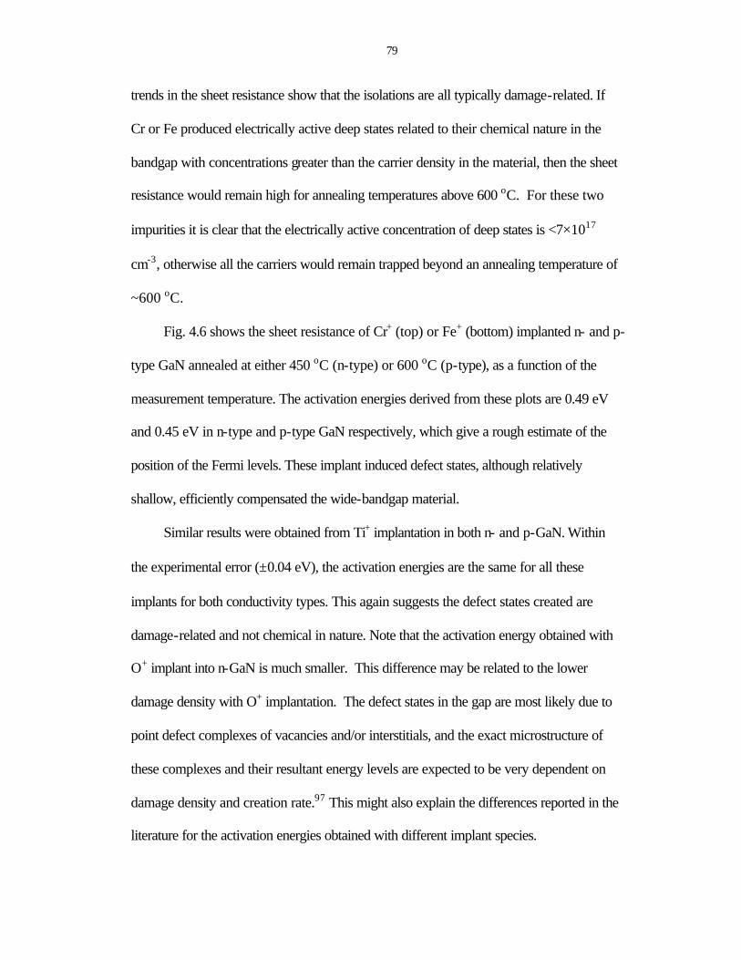
79
trends in the sheet resistance show that the isolations are all typically damage-related. If
Cr or Fe produced electrically active deep states related to their chemical nature in the
bandgap with concentrations greater than the carrier density in the material, then the sheet
resistance would remain high for annealing temperatures above 600 oC. For these two
impurities it is clear that the electrically active concentration of deep states is <7×10¹⁷
cm-3, otherwise all the carriers would remain trapped beyond an annealing temperature of
~600 oC.
Fig. 4.6 shows the sheet resistance of Cr+ (top) or Fe+ (bottom) implanted n- and p-
type GaN annealed at either 450 oC (n-type) or 600 oC (p-type), as a function of the
measurement temperature. The activation energies derived from these plots are 0.49 eV
and 0.45 eV in n-type and p-type GaN respectively, which give a rough estimate of the
position of the Fermi levels. These implant induced defect states, although relatively
shallow, efficiently compensated the wide-bandgap material.
Similar results were obtained from Ti+ implantation in both n- and p-GaN. Within
the experimental error (±0.04 eV), the activation energies are the same for all these
implants for both conductivity types. This again suggests the defect states created are
damage-related and not chemical in nature. Note that the activation energy obtained with
O+ implant into n-GaN is much smaller. This difference may be related to the lower
damage density with O+ implantation. The defect states in the gap are most likely due to
point defect complexes of vacancies and/or interstitials, and the exact microstructure of
these complexes and their resultant energy levels are expected to be very dependent on
damage density and creation rate.97 This might also explain the differences reported in the
literature for the activation energies obtained with different implant species.

80
Fig. 4.5 Evolution of sheet resistance of GaN with annealing temperature after Cr+ (top) and Fe+ (bottom) implantation.
Annealing Temperature (oC)
0 200 400 600 800 1000
Rs
(Ω/
)n-typep-type
p-type original
n-type original
Cr+→ GaN
102
104
1012
1010
108
106
102
104
1012
1010
108
106
Annealing Temperature (oC)
0 200 400 600 800 1000
Rs
(Ω/
)
n-typep-type
p-type original
n-type original
Fe+→ GaN
102
104
1012
1010
108
106
102
104
1012
1010
108
106

81
Fig. 4.6 Arrhenius plots of sheet resistance in Cr+ (top) and Fe+ (bottom) implanted n- and p-type GaN after annealing at either 450 oC (n-type) or 600 oC (p-type).
1000/T (K-1)2.0 2.4 2.8 3.2 3.6
Rs
(Ω/
)
107
108
109
1010
1011
1012
1013
Cr+ → n-GaNCr+ → p-GaN
Ea = 0.44 eV
Ea = 0.49 eV
1000/T (K-1)
2.0 2.4 2.8 3.2 3.6
Rs
(Ω/
)
108
109
1010
1011
1012 Fe+ → n-GaNFe+ → p-GaN
Ea = 0.45 eV
Ea = 0.48 eV
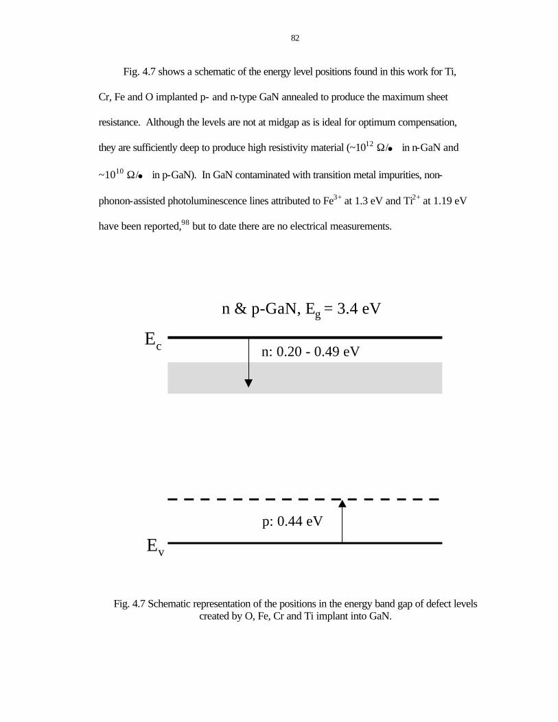
82
Fig. 4.7 shows a schematic of the energy level positions found in this work for Ti,
Cr, Fe and O implanted p- and n-type GaN annealed to produce the maximum sheet
resistance. Although the levels are not at midgap as is ideal for optimum compensation,
they are sufficiently deep to produce high resistivity material (~1012 Ω/ in n-GaN and
~1010 Ω/ in p-GaN). In GaN contaminated with transition metal impurities, non-
phonon-assisted photoluminescence lines attributed to Fe3+ at 1.3 eV and Ti2+ at 1.19 eV
have been reported,98 but to date there are no electrical measurements.
Fig. 4.7 Schematic representation of the positions in the energy band gap of defect levels created by O, Fe, Cr and Ti implant into GaN.
n & p-GaN, Eg = 3.4 eV
n: 0.20 - 0.49 eV
p: 0.44 eV
Ec
Ev

81
CHAPTER 5 ELECTRICAL CONTACTS TO GaN
5.1 Introduction
GaN is attractive for optical devices with blue or ultraviolet wavelengths as well as
for high power and high temperature electronics. Critical to the success of these devices,
however, are the ohmic contacts, and in some cases Schottky contacts to the
semiconductors. In general, making low-resistance ohmic contact is difficult for wide
bandgap materials, especially for p-type GaN due to the difficulty in doping. This creates
a large voltage drop across the GaN/metal interface for ohmic contacts, which leads to
poor device performance and reliability. For most devices, ohmic contacts with
resistances lower than 10-5 Ω⋅cm2 are desired.
Ti-based contacts with contact resistances of 10-6 – 10-5 Ω⋅cm2 have been
demonstrated on n-type GaN.23,55,99 These contacts are found to take advantages of the
formation of a thin interfacial TiN layer, which is refractory, exhibit metallic
conductivity, and possess low work function (<4 eV).100 However, no satisfying ohmic
contact to p-type GaN has been developed so far. In the search for improved contact
characteristics, a wide variety of metallizations have been investigated on p-GaN besides
the standard Ni/Au,18,56,101,102 including Ni,101,102 Au,101,103 Pd,101 Pd/Au,104 Pt/Au,105
Au/Mg/Au,106 and Pd/Pt/Au.105 Typically metals with large work function such as Ni, Pd
or Pt are in direct contact with the GaN, and the structure is annealed at 400 - 750 °C.
This produces contact resistances in the 10-1 - 10-3 Ω-cm2 range. Reports have also
83
appeared on the effect of annealing in O2 ambient in reducing rc,107 oxidation of Ni/Au
metallization and its role in improving contact quality,108 the role of surface treatments in
determining contact quality109,110 and the use of Ta/Ti contacts with low, but unstable
contact resistances.111
Another approach to achieve low-resistance contact is through semiconductor
bandgap engineering. Schubert et al.112 proposed the use of AlGaN/GaN superlattices as
a technique to increase the average hole concentration. The periodic oscillation of the
valence band edge is superimposed with the oscillation generated by pizeoelectric field,
would significantly reduce the Mg acceptor ionization energy and therefore increase the
hole concentration. Ti/Pt/Au contacts with specific contact resistance of ~4×10⁻⁴ Ω-cm2
have been achieved on this structure.113 However, this scheme may not easily be applied
to real devices, since the free carriers are separated into parallel sheets.
The Schottky contacts to n-GaN for a variety of elemental metals have been
extensively studied. The reported Schottky barrier height increases monotonically, but
does not scale proportionally with metal work function, with a considerable amount of
scatter in the experimental results for a given metal (see Fig. 2.2(b)). The I-V ideality
factor is usually significantly larger than 1, and the measured values of the Richardson’s
constant A** are quite small.54 These non-ideal behavior of GaN Schottky diodes appears
to result from the presence of several transport mechanisms, and to materials and process
factors such as defects present in these films, the effectiveness of surface cleans prior to
metal deposition, local stoichiometry variations, and variations in surface roughness.
There is not much information on Schottky contacts on p-GaN. Measurement of the
barrier height is very difficult, due to the general difficulty in growing high quality p-type

84
material, and the lack of low resistance ohmic contact. The experimental values from
conventional I-V and C-V methods are usually inconsistent, but also appear to be affected
by the work function of the metals.101
One of the important issues in making high quality Schottky and ohmic contacts to
GaN is the surface cleanliness. The ideal metal/semiconductor interface should be oxide-
and defect-free, atomically smooth, uniform, and thermally stable, with the metal
epitaxial. Analysis by spectroscopic ellipsometry showed that >30 Å of overlayer
consisting organic and inorganic, and native oxide is present on air-exposed GaN.114 In
situ treatments, such as N ion sputtering, were reported to remove oxide layer on the GaN
surface without significant modification of the N to Ga atomic ratio.101,115 For Practical
contacts, the samples are treated with various acidic or base solutions before deposition
of metal layers. It was found that HCl-based solution is more effective in removing
oxides and leaves less oxygen residue, but HF is more effective in removing carbon and
hydrocarbon contamination.116 These ex situ treatments can remove significant part of the
surface overlayer, but cannot produce atomically clean surfaces. The residual oxide layer
is expected to act as a barrier to current flow through the metal/GaN interface, therefore
has a profound influence on the electrical characteristics of contacts to GaN.
The thermal stability of metal/GaN contacts is also critically important for practical
device operation (especially power electronics). The thermal limits of most of the
metal/GaN combinations are between 300 oC and 600 oC.54 At higher temperatures,
severe degradation in contact morphology is observed, usually resulting from the
formation of new interfacial phases, such as metal gallides.

85
In this chapter, as a first step to explore the improved ohmic contact to p-GaN, the
effects of (NH4)2S treatment of the GaN surface on the electrical properties were studied.
Reductions in Schottky barrier height (SBH) by ~0.2 eV were observed. This reduction in
SBH was ascribed to removal of the native oxide of thickness 1-2 nm that was present
after conventional cleaning, and formed an interfacial insulating layer at the metal/GaN
interface. In the second part, the thermal stability of W and WSi contacts on n- and p-type
GaN was examined. Specific contact resistances in the range 10-5 Ω⋅cm2 were obtained
for W on high dose Si-implanted GaN, while true ohmic characteristics could only be
achieved at elevated temperatures for contacts on p-GaN.
5.2 Effects of Interfacial Oxides on Schottky Contact
5.2.1 (NH4)2S Treatment to Reduce Schottky Barrier Height
Three different types of samples were employed with n-type doping of either
8×1016 cm-3, or 1018 cm-3, or p-type doping (hole concentration) of 1017 cm-3. These GaN
layers were 1-3 µm thick and were grown on c-plane Al2O3 substrates by rf plasma-
assisted Molecular Beam Epitaxy. Each of the samples was treated in one of two different
ways. The first involved a conventional cleaning process that involved sequential rinsing
in acetone, isopropyl alcohol and deionized water prior to lithography for defining the
contact areas. After lithography, the samples were rinsed 60 secs in 30% HCl (25 °C)
and 30 secs in buffered HF to remove the native oxide and then immediately loaded into
the e-beam evaporator. The second cleaning process was the same as the first, but the
last step was a 20 min boil in (NH4)2S. This solution does not affect the photoresist
mask. The (NH4)2S solution is effective in removing native oxide and prevention of

86
immediate reoxidation, since a Ga-S monolayer is formed on the surface. This should be
far less of a hindrance to current flow than the presence of a much thicker native oxide.
The samples had Ti/Al or Ni/Au for ohmic contacts, each annealed at 750 °C for 30 secs
to produces low rc. The Pt (400 Å)/Au (1500 Å) rectifying contacts were e -beam
deposited with diameters 50-200 µm. The effective barrier heights were obtained from
the forward current-voltage (I-V) characteristics, according to the eq. 2.6
]1))[exp(exp(2** −−=nkTeV
kTTAJ bφ
where A** is 26.4 A· cm-2· K-2 for n-GaN, 96.1 A· cm-2· K-2 for p-GaN.
Fig. 5.1 shows forward (top) and reverse (bottom) I-V characteristics from the n+
GaN diodes, either with or without the (NH4)2S treatment prior to Schottky contact
deposition. There are several key points in this data. First, the forward current increases
as a result of the (NH4)2S treatment due to a decrease in barrier height from 0.81 eV on
the control diode to 0.58 eV on the treated diode. Second, in the linear region of the
forward characteristics, the scaling of current with contact diameter is much greater than
a power of two. This suggests that there is a non-uniform concentration of defects, which
are generation-recombination centers. Finally, the reverse leakage current is also
increased by the (NH4)2S treatment.
Similar data is shown in Fig. 5.2 for the n-GaN diodes, at two different rectifying
contact diameters. The average barrier height decreased from ~0.99 eV on the control
diodes to ~0.83 eV on the (NH4)2S treated samples. Both the forward and reverse current
increased as a result of the (NH4)2S step.
Fig. 5.3 shows I-V characteristics from the p-GaN diodes. These structures showed
high currents due to the difficulty in forming high barriers to p-GaN. The control diodes
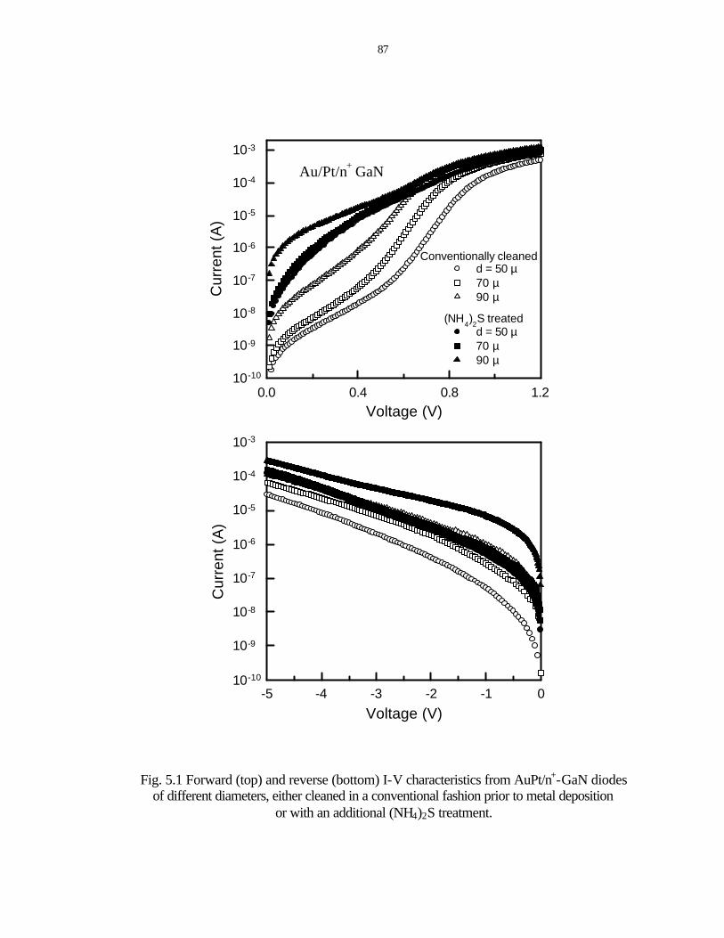
87
Fig. 5.1 Forward (top) and reverse (bottom) I-V characteristics from AuPt/n+-GaN diodes of different diameters, either cleaned in a conventional fashion prior to metal deposition
or with an additional (NH4)2S treatment.
Voltage (V)0.0 0.4 0.8 1.2
Cur
rent
(A
)
10-10
10-9
10-8
10-7
10-6
10-5
10-4
10-3
d = 50 µ70 µ90 µ
d = 50 µ70 µ90 µ
Conventionally cleaned
(NH4)2S treated
Au/Pt/n+ GaN
Voltage (V)-5 -4 -3 -2 -1 0
Cur
rent
(A
)
10-10
10-9
10-8
10-7
10-6
10-5
10-4
10-3

88
Fig. 5.2 Forward (top) and reverse (bottom) I-V characteristics from AuPt/n--GaN diodes of different diameters, either cleaned in a conventional fashion prior to metal deposition
or with an additional (NH4)2S treatment.
Voltage (V)0.0 0.4 0.8 1.2 1.6
Cu
rre
nt
(A)
10 -11
10 -10
10 -9
10 -8
10 -7
10 -6
10 -5
10 -4
10 -3
d=50 µd=200 µ
d=50 µd=200 µ
Conventionally cleaned
(NH4)2S treated
Voltage (V)
-8 -6 -4 -2 0
Cu
rre
nt
(A)
10-11
10-10
10-9
10-8
10-7
10-6
10-5
(NH4)2S treated

89
showed average barrier heights of 0.49 eV, which was slightly reduced to 0.47 eV as a
result of the (NH4)2S treatment. In these diodes the low bias current scaled with contact
diameter, indicating that surface leakage is important. We did not passivate the
perimeters of the devices in this work.
Fig. 5.3 I-V characteristics from AuPt/p-GaN diodes of different diameters, either cleaned in a conventional fashion prior to metal deposition or with an additional (NH4)2S
treatment.
Voltage (V)
-0.4 -0.2 0.0 0.2 0.4
Cur
rent
(µA
)
-10
-5
0
5
10
d = 50 µ90 µ200 µ
50 µ90 µ200 µ
Conventionally cleaned
(NH4)2S treated
Au/Pt/p-GaN

90
Table 5.1 shows a compilation of the barrier heights and ideality factors for the n+,
n and p diodes. The clear effect of the boiling (NH4)2S exposure is to decrease φb ,
suggesting it could be promising for fabrication of high quality ohmic contacts on GaN.
(NH4)2S solution was also employed to treat completed GaN mesa Schottky diodes. Fig.
5.4 shows I-V characteristics from control and the passivated devices. Both the forward
and reverse current densities increase slightly after the treatment. This probably can be
ascribed to the same reason as described earlier, i.e. (NH4)2S passivation reduced the
barrier height, and the leakage current on the periphery increased. The forward section of
the I-V characteristics shows only a slight improvement in ideality factor, and little
change in this parameter is also showed in Table 5.1. Note that the 2kT leakage current in
a diode of this type has contributions from both the bulk space-charge region and the
mesa surface, and that sulfide passivation would only affect the latter. The fact that the
Table 5.1. Summary of electrical data for test diodes.
n φb (eV)
Sample Conventionally
cleaned (NH4)2S treated
Conventionally cleaned
(NH4)2S treated
AuPt/ n+-GaN
1.6-1.8 1.8-1.9 0.81 0.58
AuPt/ n-GaN
1.4-1.6 1.3-1.8 0.99 0.83
AuPt/ p-GaN
~2 ~2 0.49 0.47

91
diode ideality factors did not improve suggests that the problem for the conventional III-
V compound semiconductors, i.e. high density of surface states, is absent for GaN, and
(NH4)2S does not passivate the surface of GaN electronically, as it for the GaAs or InP
surfaces. This is consistent with the fact that no Fermi level pinning has been observed on
the GaN surface. However we generally got ideality factors much larger than unity,
which indicates high dislocation densities and high compensation levels in the current
state of GaN materials. Particularly for diodes fabricated on MBE grown wafers, high
leakage currents were typically observed, due to relatively low epi thickness of this
growth method.
Fig. 5.4 I-V characteristics from complete GaN mesa diodes before and after (NH4)2S treatment.
Voltage (V)
-15 -10 -5 0 5
Cur
rent
(A
)
-0.006
-0.004
-0.002
0.000
0.002
control(NH4)2S passivated
0.2 0.4 0.6 0.8 1.010-7
10-6
10-5
10-4
10-3

92
5.2.2 Interfacial Insulator Model
A contamination layer such as a thin oxide at the metal/semiconductor interface
usually behaves as an insulator, and provides energy barrier for carrier injection. It is
assumed that the thickness and the mean tunneling barrier height of this thin oxide layer
are δ and χ, respectively. According to the Quantum Mechanics, the transmission
coefficient of an electron with energy E through this barrier is given by:
])()2(2
exp[][)2(2
exp 2/12/12/1
0
2/1 δχχδ
EmdxEmT −−=−−≈ ∫ hh (5.1)
where m is the tunneling effective mass. Therefore, the current density across the
interface can be expressed as (the zero of electron energy is chosen as the conduction
band edge at the semiconductor surface) :
Jqm
m f f dE dEts m t x= − −
∞ ∞
∫ ∫22
22 31 2
0 0πχ δ
h hexp[ ( ) ] ( )/ (5.2)
where Ex and Et are the electron energy components normal and parallel to the Schottky
barrier; fs and fm are the Fermi-Dirac distribution functions for electron states in the
semiconductor and metal, respectively; and mt is the effective mass component in the
semiconductor transverse to the barrier. In the nondegenerate case, the current density for
forward biases V>3kT/q is given by:
J A T m q kT qV nkTb= − −** /exp[ ( ) ]exp( / )exp( / )2 1 20
22
hχ δ φ (5.3)
Compared with eq. 2.7 The effective SBH φb can be obtained:
φ φ φb b= +0 ∆ (5.4)

93
where φb0 is the barrier height without the interfacial layer and ∆φ is the additional
barrier due to the oxide. The parameter ∆φ is given by 2
21
2kTm
h( )χ δ . The χ value for
the oxide on GaN is calculated to be ~0.2 eV using the free electron mass.101 In this work
we typically observed ∆φ to be 0.16-0.23 eV for Pt/Au on n-GaN, which yields an
estimate for oxide layer thickness of 1-2 nm left on the GaN surface after conventional
cleaning. Previous work on the effect of different surface treatments on the rc of ohmic
contacts on p-GaN has shown that wet chemical solutions that remove the native oxide
improve the contact resistance. For example, solutions of 1 HNO3 : 3 HCl were found to
produce rc values of 4.1×10⁻⁴ Ω⋅cm2 for Pd/Au ohmic contacts on p-GaN, whereas
untreated samples had values two orders of magnitude larger.109 Similarly the use of
buffered HF and boiling (NH4)2S, followed by a final dip in buffered HF prior to metal
deposition was able to lower rc by 3 orders of magnitude relative to untreated diodes.117
The oxide can also be removed by annealing the contact metal at elevated temperatures.
Ishikawa et al.101 observed that for Ni/GaN or Ta/GaN contacts, Ni or Ta diffused into
the contamination layer after annealing at 500 oC, and grew epitaxially on the GaN
surface. However, Au and Pd did not react efficiently with the oxide layer. Our work
suggests that the conventional ex situ surface treatments using HCl and HF can not
completely remove the native oxide on GaN. This oxide has a strong influence on the
contact characteristics on both n- and p-type GaN, and appears to be responsible for some
of the wide spread in contact properties reported in the literature.
Fig. 5.5 shows the band diagrams for metal/n or n+ GaN structures either with an
interfacial oxide (top) and after boiling in (NH4)2S to remove this oxide (bottom). In the
case of n-GaN the dominant current conduction mechanism probably remains as

94
thermionic field emission (albeit with low barrier height), while for n+ GaN there may
also be a contribution from field emission. Alternative explanations for the increased
current in (NH4)2S-treated samples would be an increase in contact area due to surface
roughening. However AFM measurements showed no significant change in the root-
mean-square surface roughness in our samples.
Fig. 5.5 Energy band diagrams at the interface of n+-GaN/metal and n--GaN/metal with or without an interfacial oxide layer.
φbEF EC
EV
δ
n+-GaNmetal φb
EF EC
EV
δ
n--GaNmetal
φb0EF EC
EV
n+-GaNmetal φb0
EF EC
EV
n--GaNmetal
thermionic emission thermionic emission
field emission thermionic field emission

95
5.3 Thermally Stable W-based Ohmic Contact
5.3.1 W on Si-implanted GaN
Undoped GaN layers ~3 µm thick were grown on Al2O3 by Metal Organic
Chemical Vapor Deposition. These samples were implanted with 150 keV Si+ ions at a
dose of 5 × 1015 cm-2 and annealed with AlN caps in place to 1400 °C for 10 secs, as
described in Chapter 2. W or WSi0.45 layers ~ 1000 Å thick were deposited using an
MRC501 sputtering system. The sample position was biased at 90 V with respect to the
Ar discharge. Prior to sputtering, the surface contamination was removed by a rinse in
HCl and buffered HF solutions. Transmission line patterns were defined by dry etching
the exposed metal with SF6/Ar, and forming mesas around the contact pads using
BCl3/N2 dry etching to confine the current flow. The samples were annealed for 60 secs
at 500 - 1100 °C under flowing N2.
The Si implantation followed by high temperature activation yielded about a peak
n-type doping concentration of ~5 × 1020 cm-3. For as-deposited metal contacts on this
highly doped layer, tunneling current dominates the total current. The specific contact
resistance is roughly determined by the tunneling mechanism, i.e. eq.2.13. Fig. 5.6 shows
the annealing temperature dependence of rc for W contacts on Si-implanted GaN. The
specific contact resistance improves with annealing up to ~950 °C, and degrades at high
temperatures. Cole et al.118 observed the formation of the β-W2N phase at W/GaN
interface at annealing temperatures between 600 oC and 1000 oC, as demonstrated by the
x-ray results in Fig. 5.7. The as deposited sample displays a well oriented (110) W film
overlaying a well oriented (002) GaN epilayer. The sample annealed at 800 oC exhibits a
well developed face cubic β-W2N phase as indicated by diffraction peaks from (111),

96
Fig. 5.6 Specific contact resistance for W on Si+ implanted GaN, as a function of post-metallization annealing temperature.
(200), (220) and (311) planes. The onset of the formation of this thin compound was first
detected after annealing at 600 oC. Annealing at 1000 oC caused this phase to disorder, as
reflected by the broaden W2N(111) as well as the disappearance of the other W2N peaks.
The β-W2N phase was no longer stable and subsequently transformed into the defect
structure of W-N after annealing at higher temperatures.
Temperature (oC)
400 500 600 700 800 900 1000 1100
Rc (
oh
m-c
m2)
10-6
10-5
10-4
10-3
W/Si+-implanted GaN
30 second anneals

97
Fig. 5.7 The x-ray diffraction results for the (a) as-deposited, (b) 800 oC annealed, (c) 1000 oC annealed W on n+-GaN samples.
As-deposited
800 oC
1000 oC
2θ
Inte
nsity
(cp
s)

98
The formation of the β-W2N phase paralleled the low specific contact resistance,
and is very likely to be critical for achieving the low resistance W ohmic contacts on
GaN. If the N needed to form this interfacial compound has out-diffused from the GaN
without discomposing the original structure, then there would exist an accumulation of N
vacancies near the GaN surface, which act as donors. Thus the surface GaN would be
highly n-type and the carrier tunneling is enhanced. Another possibility is that the N out-
diffusion aids in the formation of a Ga enriched highly conductive layer at the GaN
surface, and results in a lower barrier height.
The near surface GaN crystal quality is of particularly importance, and could
directly influence the uniformity and stability of the W contacts. TEM results showed that
the defect laden regions were directly associated with contact spiking into the GaN
epilayer, which in turn inhibited the formation and development of the β-W2N interfacial
phase with its associated smooth metal semiconductor interface.119 Protrusion of the
metallization down the threading and misfit dislocations was observed at 800 oC,
extending >5000 Å in some cases, which is obviously a problem for multilayer structures.
In a contrast, contacting to a low defect surface improved the lateral extent of the new
phase needed for ohmic contact formation and impeded contact metal spiking. The
excellent structural stability of the W on GaN is shown in the SEM micrographs of Fig.
5.8, where a sharp interface is retained after 750 °C annealing.
5.3.2 Behavior of W and WSi Contacts on p-GaN
The 1 µm thick GaN layers were grown on Al2O3 substrates by Molecular Beam
Epitaxy using solid Ga and rf-activated N2 from a plasma source. The Mg acceptor
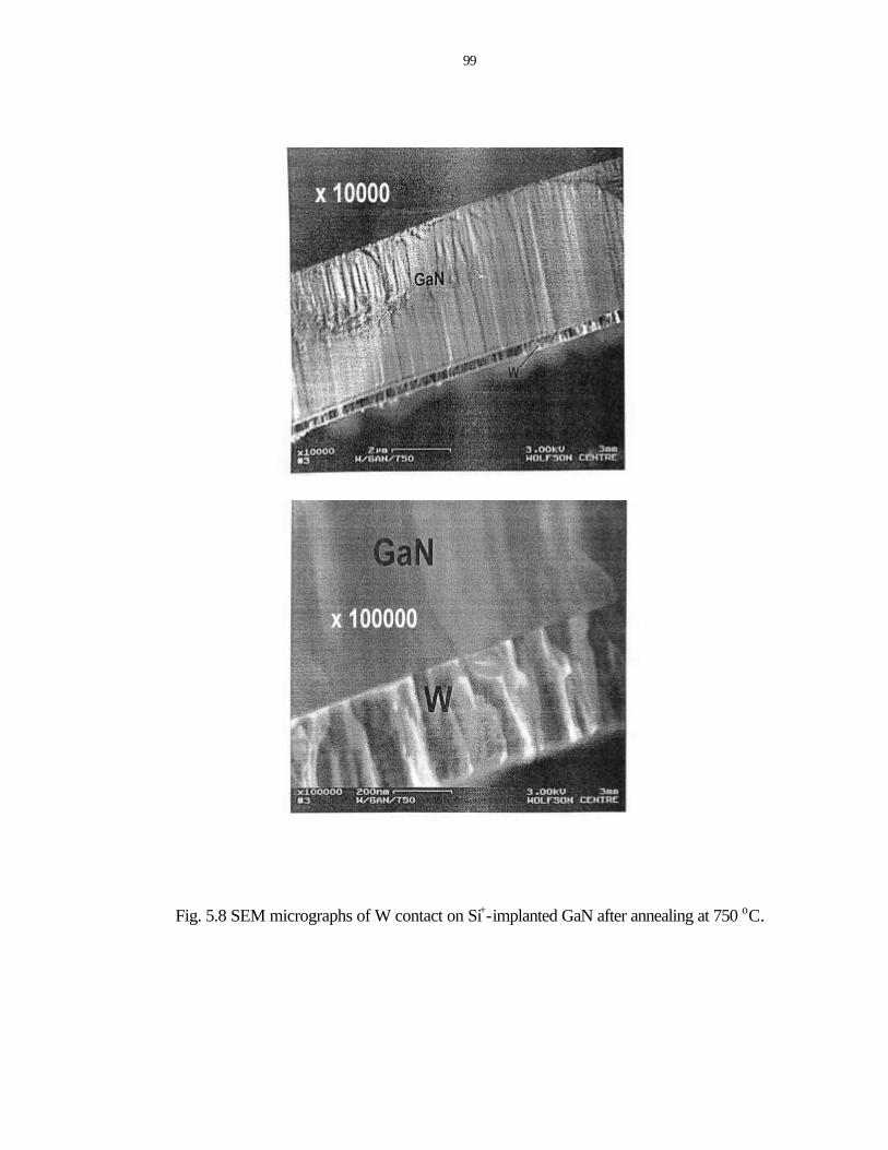
99
Fig. 5.8 SEM micrographs of W contact on Si+-implanted GaN after annealing at 750 oC.

100
concentration was 1018 cm-3. Cathodoluminescence revealed a strong peak at 383-385
nm, with very little deep level emission. W or WSi0.45 layers ~1000 Å thick were
deposited using an MRC501 sputtering system using an Ar discharge and an acceleration
voltage of 90 V. Prior to sputtering, the samples were cleaned in HCl and buffered HF
solutions. TLM patterns were defined by dry etching the exposed metal with SF6/Ar, and
forming mesas around the contact pads using BCl3/N2 dry etching to confine the current
flow. For comparison Au(1000 Å)/Ni(500 Å) was deposited by e -beam evaporation,
defined by lift-off and mesas formed by dry etching. The samples were annealed for 1
minute at temperatures from 400 - 1100 °C under a flowing N2 ambient.
Fig. 5.9 shows I-V characteristics for WSi, W and Ni/Au metallization on p-GaN,
as a function of post-deposition annealing temperature. It is clear that annealing at low
temperatures improves the intimate contact between the metals and GaN, therefore, the
contact quality. However, even at the optimum annealing temperatures for each metal
scheme (700 °C for Ni/Au and W; 800 °C for WSix), there is not true ohmic behavior,
and the contacts are better described as leaky Schottky diodes. At annealing temperatures
above these optimum conditions, the contact characteristics worsen and become more
rectifying. Note that the formation of the W2N phase at these temperatures could result in
a decrease in hole concentration at the GaN surface, and degrades the contact properties.
It is instructive to examine the contact morphology for different annealing
temperatures. Fig. 5.10 shows scanning electron micrographs of Ni/Au after annealing at
400 °C (top left) and 700 °C(top right), and of W after annealing at 400 °C (bottom left)
or 900 °C (bottom right). In the former case the Ni/Au becomes strongly islanded, as
reported by Venugopalan et al.120 due to dissociation of the GaN by the reaction with the

101
Fig. 5.9 Annealing temperature dependence of I-V characteristics of WSi, W and Ni/Au contacts on p-GaN (60 s anneal times).
Voltage (V)
-4 -2 0 2 4
WSi/p-GaN
Cu
rre
nt
(A)
as-deposited400 oC500 oC600 oC700 oC800 oC900 oC
W/p-GaN
Au/Ni/p-GaN
2 x 10⁻⁵
-2 x 10⁻⁵
0
0
0
-2 x 10⁻⁵
2 x 10⁻⁵
2 x 10⁻⁵
2 x 10⁻⁵
700 oC
800 oC

102
Fig. 5.10 SEM micrographs of Ni/Au contacts on p-GaN after 60 s anneals at 400 oC (top left) or 700 oC (top right), and W contacts after annealing at 400 oC (bottom left) or 900
oC (bottom right).
Ni.56 The rate of the reaction becomes increasingly rapid above ~600 °C, and in our
contacts a 5 min anneal at 700 °C produced extremely poor results both from an electrical
and structural view point. The reacted nature of the Ni/Au contact will definitely be a
problem in electronic devices such as heterojunction bipolar transistors or junction field
effect transistors, where the contact size is much smaller than in photonic devices, and
need to be uniform for large numbers of devices. By sharp contrast, both the W and WSi
did not show any loss of dimensional stability or surface morphology degradation even at

103
> 900 °C. In addition, there is not a strong dependence of the electrical characteristics on
annealing time, as shown in Fig. 5.11. There is little change in the contact properties for
30 secs - 2 mins, and contacts become slightly more rectifying for longer time, indicating
the interfacial reaction is very limited. In conjunction with the low defect density material
grown by epitaxial overgrowth, the use of WSi and W metallization should prove useful
in improving the thermal stability of p-ohmic contacts on GaN.
Fig. 5.11 Annealing time dependence at 700 oC of I-V characteristics from W contacts on p-GaN.
Voltage (V)
-2 -1 0 1 2
Cu
rre
nt (A
)
30 s1 min2 min3 min5 min
W/p-GaN
700 oC annealing
2 x 10⁻⁵
1 x 10⁻⁵
-2 x 10⁻⁵
-1 x 10⁻⁵
0

104
From Fermi - Dirac statistics we can calculate the Fermi level position EF for p-
GaN containing 1018 acceptors ⋅ cm-3 as a function of absolute temperature T, from
NA)/)exp((21
1kTEE Fa −+
= NV exp(-(EF-EV)/kT) (5.5)
where NA is the acceptor concentration, Ea = 171 meV for Mg in GaN and NV is the
valence band density of states. Using this relation, we calculated the ionization efficiency
for Mg as a function of sample temperature, as shown in Fig. 5.12. At 25 °C, only ~10%
of the Mg is ionized, whereas the efficiency increases to ~57% at 300 °C. Given the
acceptor concentration in our films, this means the hole density rises from ~1017 at 25 °C
to ~5.7×1017 cm-3 at 300 °C. Past investigations have shown a combination of thermionic
emission and thermionic field emission as the dominant conduction mechanisms in
contacts to p-GaN.105,121 At elevated operating temperatures, the hole density in the
material increases rapidly, leading to a decrease in material sheet resistance. Concurrently
there should be more efficient thermionic emission and tunneling of holes across the
metal - GaN barrier, leading to a decrease in specific contact resistance. Fig. 5.13 shows I
- V characteristics from the three different metallization schemes on p-GaN, as a function
of measurement temperature. At 250 °C the Ni/Au is truly ohmic, whereas the W and
WSix have linear characteristics at 300 °C. Table 5.2 shows the rc values at 300 oC are 9.2
× 10-2 Ω-cm2 (Ni/Au), 6.8 × 10⁻¹ Ω-cm2 (W) and 2.6 × 10⁻² Ω-cm2 (WSi). The substrate
sheet resistance decreases with increasing temperature, indicating that the increased hole
comncentration plays a major role in decreasing rc. Whilst device operation at elevated
temperatures clearly would improve the p-contact resistance, it remains to be seen how
much of a trade-off this entails in terms of degraded reliability.

105
Table 5.2. Temperature-dependent contact data for p-GaN.
Contact
Measurement temperature (oC)
Specific contact resistance (Ω-cm2)
Contact resistivity (Ω-mm)
Sheet resistance (Ω/)
Ni/Au 200 0.125 415.7 13900
Ni/Au 250 0.121 319.5 8470
Ni/Au 300 0.092 205.9 4600
W 300 0.682 758.4 -
WSi 300 0.026 1728.3 -
Fig. 5.12 Ionization efficiency of Mg acceptors in GaN, and Fermi-level position for GaN doped with 1018 cm-3 Mg acceptors as a function of temperature.
Temperature (oC)
0 100 200 300
Ioni
zatio
n ef
ficie
ncy
(%)
0
10
20
30
40
50
60
EF-E
V (
meV
)
120
140
160
180
200
220
240
Mg in GaN 1x1018 cm-3
EA - EV = 171 meV

106
Fig. 5.13 Measurement temperature dependence of I-V characteristics of Ni/Au, W and
WSi contacts on p-GaN.
Voltage (V)
-0.4 -0.2 0.0 0.2 0.4
WSi/p-GaN
Cur
rent
(A
)
W/p-GaN
Au/Ni/p-GaN
-4 x 10⁻⁶
0
4 x 10⁻⁶
1.2 x 10⁻⁵
0
-1.2 x 10⁻⁵
2 x 10⁻⁵
0
-2 x 10⁻⁵
RT100 oC150 oC200 oC250 oC300 oC

106
CHAPTER 6 DRY ETCH DAMAGE IN GaN
6.1 Introduction
Dry etching has proven an effective technique for the formation of mesas in GaN
devices. However, exposure to the energetic ions may result in significant damage, which
often degrades the material properties and device performance. ICP technique uses lower
ion energies than RIE, and thus in general has lower damage levels as a result. At high
source powers, however, ion flux incidence on the surface is so high that substantial
damage can be detected to depths of a few hundred angstrom. Plasma induced damage to
GaN may take several forms, all of which lead to changes in its electrical and optical
properties, as follows:
1. Ion induced creation of lattice defects which generally behave as deep level states
and thus produce compensation, trapping or recombination in the material. Due to
channeling of the low energy ions that strike the sample, and rapid diffusion of the
defects created, the effects can be measured as deep as 1000 Å from the surface,
even though the projected range of the ions is only ≤10 Å.
2. Unintentional passivation of dopants by atomic hydrogen. The hydrogen may be a
specific component of the plasma chemistry, or may be unintentionally present
from residual water vapor in the chamber or from sources such as photoresist mask
erosion. The effect of the hydrogen deactivation of the dopants is a strong function
of substrate temperature, but may occur to depths of several thousand angstroms.

108
3. Creation of non-stoichiometric surfaces through preferential loss of one of the
lattice elements. This can occur because of strong differences in the volatility of the
respective etch products, leading to enrichment of the less volatile species, or by
preferential sputtering of the lighter lattice element if there is a strong physical
component to the etch mechanism. Typical depths of this non-stoichiometry are
<100 Å.
4. Deposition of polymeric film from plasma chemistries involving CHx radicals, or
from reaction of photoresist masks with Cl2-based plasma.
In GaN-based photonic devices, the constraints placed on dry etching are minimal.
Usually these structures are heavily doped, and etch depths are comparatively large, and
thus are fairly resistant to damage. Moreover, the etch proceeds to a n+ GaN layer, onto
which an ohmic contact is subsequently deposited. Preferential loss of N2 from the near-
surface region during the etch step is actually beneficial in this case because it leads to
increased n-type doping levels and hence lower contact resistances.99,122,123 By sharp
contrast, in electronic devices such as HBTs or BJTs, the etching requirements are much
more demanding. Low damage processes are required to form mesas for the base and
collector contacts without increasing recombination in the base-emitter junction or
surface leakage in the base-collector junction.
To date, much less is known about the electrical effects of dry etch damage, and its
subsequent removal by chemical treatment or annealing in the GaN system than in other
compound semiconductors. Most past work in this area has focussed on n-type material.
The sheet resistances of GaN, InGaN, InAlN and InN samples were found to increase in
proportion to ion flux and ion energy in an ECR Ar plasma.124,125 Ren et.al.126 examined

109
the effect of ECR BCl3/N2 and CH4/H2 plasmas on the electrical performance of InAlN
and GaN channel field effect transistors. They found that hydrogen passivation of the Si
doping in the channel may occur if H2 is a part of the plasma chemistry and that
preferential loss of N2 degraded the rectifying properties of Schottky contacts deposited
on plasma-exposed surfaces. Saotome at al.127 found pure Cl2 plasma treatment decreased
near band-edge PL intensity of the GaN samples by a factor of approximately five
through introduction of non-radiative levels, whereas subsequent photo-assisted wet
etching restored this to about half of the original value.
There is very little information available on the electrical effects of plasma damage
in p-type GaN. Shul et.al.128 reported that the sheet resistance of p-GaN increased upon
exposure to pure ICP Ar discharge. The increases were almost linearly dependent on ion
energy, but weakly dependent on ion flux.
In this chapter, we studied systematically the effects of ICP N2, H2, Ar or Cl2/Ar
discharge exposure under various conditions on the properties of n- and p-GaN Schottky
diodes. The choice of these plasma chemistries enabled us to differentiate between ion
mass effects and the role of physical versus chemical components of the etching. The
depth and thermal stability of the damage has been determined. Wet etching and thermal
annealing were employed to restore the electrical properties of the damaged materials.
6.2 Plasma Damage in n-GaN
6.2.1 Comparison of N2 and H2 Discharge Exposure
The layer structure and contact metals are shown schematically in Fig. 6.1. The
GaN was grown by rf plasma-assisted Molecular Beam Epitaxy on c-plane Al2O3

110
substrates. The Ti/Au Ohmic contacts were pattern by lift-off and annealed at 750 oC,
producing contact resistances in the 10-4 Ω⋅cm-2 range. Samples were exposed to either
pure N2 or H2 discharges in a Plasma Therm 790 ICP system at a fixed pressure of 5
mTorr. The gases were injected into the ICP source at a flow rate of 15 standard cubic
centimeters per minute (sccm). The experimentally varied parameters were source power
(300-1000 W) and rf chuck power (40-250 W), which control ion flux and ion energy,
respectively. The Pt/Au Schottky metallization was then deposited through a stencil mask
by e-beam evaporation. I-V characteristics were recorded on a HP4145A parameter
analyzer, and the reverse breakdown voltage (VB) was defined as the voltage at which the
leakage current was 5×10⁻³ A. We found in all cases that plasma exposure caused
significant increases in forward and reverse currents, with ideality factors increasing from
typical values of 1.4-1.7 on control samples to >2. For this reason we were unable to
extract meaningful values of either ideality factor or barrier height.
Fig. 6.1 Schematic of GaN Schottky diode structure.
Pt/AuTi/Au Ti/Au
0.5 µm n+ (1018 cm-3) GaN
Al2O3 substrate
3 µm undoped (n~1017 cm-3) GaN

111
Fig. 6.2 shows a series of I-V characteristics from the GaN diodes fabricated on
samples exposed to either H2 or N2 discharges at different source powers. It is clear that
N2 plasma exposure creates more degradation of the diode characteristics than does H2
exposure. This implicates the ion mass (28N2+, 2H2
+ for the main positive ion species) as
being more important in influencing the electrical properties of the GaN surface than a
chemical effect, since H2 would be likely to preferentially remove nitrogen from the GaN
as NH3.
The variations of VB of the diodes with the source power during plasma exposure
are shown in Fig. 6.3. For any exposure to the N2 discharges, VB is severely reduced. By
contrast there is less degradation with the H2 plasma exposures at higher source powers.
This is likely related to the lower average ion energy at those conditions, as shown at the
bottom of Fig. 6.3. The average ion energy is approximately equal to the sum of dc self-
bias and plasma potential, with the latter being in the range -22 to -28 V as determined by
Langmuir probe measurements. Ion induced lattice damage in GaN may display n-type
conductivity, due to more N atom displaced. In addition, the heavy N2+ ions are also more
effective in preferential sputtering of the N relative to Ga and creating N vacancy,
compared to the H2+ ions. The net result is that N2
+ ions will lead to more degradation of
the surface electrical properties of GaN than do H2+ ions of similar energy.
Similar conclusions can be drawn from the data on the effect of increasing rf chuck
power. Fig. 6.4 shows the diode I-V characteristics from H2 or N2 plasma exposed
samples at fixed source power (500 W) but varying rf chuck power. There are once again
very severe decreases in breakdown voltage and increases in leakage current. The
dependence of VB on rf chuck power during the plasma exposures is shown in Fig. 6.5,
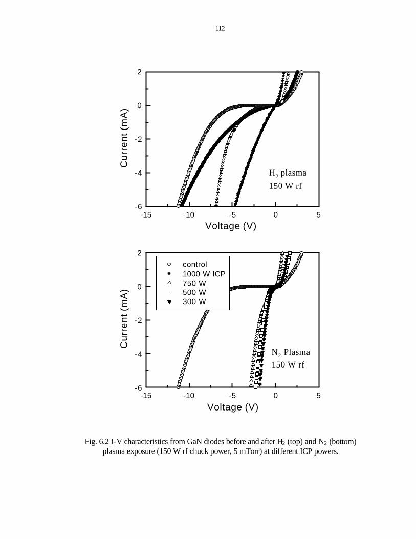
112
Fig. 6.2 I-V characteristics from GaN diodes before and after H2 (top) and N2 (bottom) plasma exposure (150 W rf chuck power, 5 mTorr) at different ICP powers.
Voltage (V)-15 -10 -5 0 5
Cu
rre
nt
(mA
)
-6
-4
-2
0
2
H2 plasma
150 W rf
Voltage (V)-15 -10 -5 0 5
Cu
rre
nt
(mA
)
-6
-4
-2
0
2
control1000 W ICP750 W 500 W300 W
N2 Plasma150 W rf

113
Fig. 6.3 Variation of VB in GaN diodes (top) and dc chuck self-bias (bottom) as a function of ICP source power in H2 or N2 plasmas (150 W rf chuck power, 5 mTorr).
Source Power (W)
0 200 400 600 800 1000 1200
VB (
V)
0
4
8
12
H2
N2
Source Power (W)
200 400 600 800 1000 1200
dc S
elf-
bias
(V
)
120
160
200
240
280
H2
N2

114
along with the dc self bias. The VB values fall by more than a factor of two even for very
low self-biases, and emphasize how sensitive the GaN surface is to degradation by
energetic ion bombardment. The degradation saturates beyond ~100 W chuck power,
corresponding to ion energies of ~175 eV. We assume that once the immediate surface
becomes sufficiently damaged, the contact properties basically cannot be made any worse
and the issue is then whether the damage depth increases with the different plasma
parameters. Since ion energy appears to be a critical factor in creating the near-surface
damage, damage depth would be expected to increase with ion energy in a non-etching
process. In the case of simultaneous etching and damage creation (e.g. in Cl2/Ar etch
processing), higher etch rates would lead to smaller depth of residual damage because the
disordered region would be partially removed.
For completed n-GaN diodes exposed to ICP discharges, we observed the changes
in the electrical properties were much less severe than those above. However, the low
bias forward currents of the damaged devices were still increased by up to two orders of
magnitude. Auger Electron Spectroscopy showed that plasma exposure created a N2-
deficient region arround the periphery of the rectifying contact, which reduced the barrier
to current conduction. By contrast, the reverse I-V is more strongly dependent on the bulk
doping in the GaN under the contact and is less affected by the plasma damage.
6.2.2 Effect of Etching Chemistries on Damage
It would be expected that exposure to etching chemistries such as Cl2/Ar create less
and shallower damage, on the basis of the fast etching rate and hence improved damage
removal. In this section we compare the effects of Cl2/Ar and Ar ICP exposure on the

115
Fig. 6.4 I-V characteristics from GaN diodes before and after H2 (top) or N2 (bottom) plasma exposure (500 W source power, 5 mTorr) at different rf chuck powers.
Voltage (V)-15 -10 -5 0 5
Cur
rent
(mA
)
-6
-4
-2
0
2
control sample40 W rf100 W rf150 W rf250 W rf
H2 Plasma500 W ICP
Voltage (V)-15 -10 -5 0 5
Cur
rent
(mA
)
-6
-4
-2
0
2
N2 Plasma500 W ICP
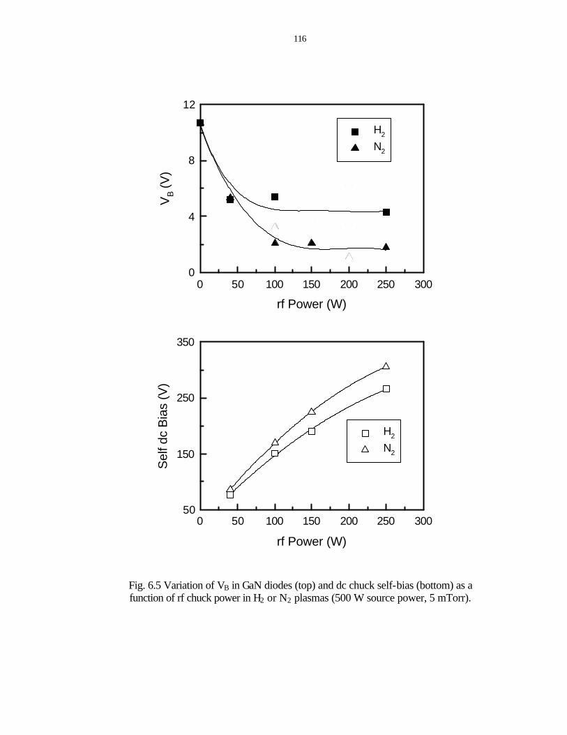
116
Fig. 6.5 Variation of VB in GaN diodes (top) and dc chuck self-bias (bottom) as a function of rf chuck power in H2 or N2 plasmas (500 W source power, 5 mTorr).
rf Power (W)
0 50 100 150 200 250 300
VB (
V)
0
4
8
12
H2
N2
rf Power (W)
0 50 100 150 200 250 300
Sel
f dc
Bia
s (V
)
50
150
250
350
H2
N2

117
electrical properties of n-GaN Schottky diodes. The layer structure consisted of 0.5 µm n+
(1018 cm-3) GaN grown on c-plane Al2O3 substrate by MBE, followed by 1 µm of
nominally doped (n~5×1016 cm-3) GaN. The mesas were etched with Ar/Cl2 ICP
discharges at low powers, and ohmic contacts were formed by e-beam evaporation and
lift-off of Ti/Al/Pt/Au, followed by annealing at 800 oC to remove dry etch damage and
alloy the contacts. The samples were exposed to either 10Cl2/5Ar or 15Ar (where the
numbers denote the gas flow rate in standard cubic centimeters per minute) ICP
discharges in a Plasma-Therm ICP reactor at a fixed pressure of 3 mTorr. We
investigated a range of rf chuck powers (25-250 W) and etch times (4-100 secs), with a
fixed source power of 500 W. The Schottky metallization Pt/Au (φ= 50, 70 or 90 µm)
was then deposited on the damaged surface by e-beam evaporation, followed by lift off.
Schematic of the mesa diodes and a SEM micrograph are shown in Fig. 6.6.
Fig. 6.7 shows a series of I-V characteristics from n-type GaN diodes fabricated on
samples exposed to either Cl2/Ar (top) or Ar (bottom) discharges at different rf chuck
powers. There is a significant reduction in VB under all conditions, with Ar producing
less damage at low chuck powers. This is probably related to two factors – the slightly
higher chuck bias with Cl2/Ar due to the lower positive ion density in the plasma (Cl is
more electronegative than Ar) and the heavier mass of the Cl2+ ions compared to Ar+.
This is consistent with data on the relative effects of N2 and H2 plasma exposure, i.e. ion
mass was more important in influencing the electrical properties of the GaN surface than
any chemical effects.
The variations of VB and VF with the rf chuck power during plasma exposure are
shown in Fig. 6.8 (top). At powers ≤100 W (this correspond to ion energies <~150 eV),

118
Fig. 6.6 Schematic of the diode structure (top) and SEM of a complete device (bottom).
Pt/Au
Ti/Al Ti/Al
0.5 µm n+-GaN
Al2O3 substrate
1 µm n--GaN
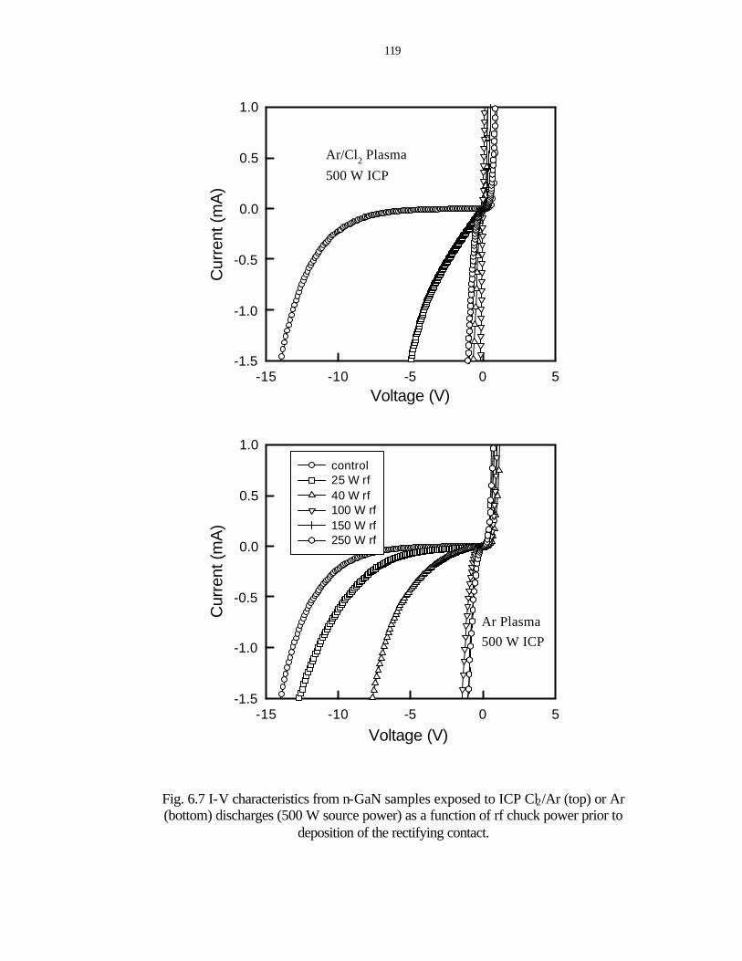
119
Fig. 6.7 I-V characteristics from n-GaN samples exposed to ICP Cl2/Ar (top) or Ar (bottom) discharges (500 W source power) as a function of rf chuck power prior to
deposition of the rectifying contact.
Voltage (V)-15 -10 -5 0 5
Cur
rent
(m
A)
-1.5
-1.0
-0.5
0.0
0.5
1.0
control25 W rf40 W rf100 W rf150 W rf250 W rf
Ar Plasma500 W ICP
Voltage (V)-15 -10 -5 0 5
Cur
rent
(m
A)
-1.5
-1.0
-0.5
0.0
0.5
1.0
Ar/Cl2 Plasma
500 W ICP

120
Fig. 6.8 Variations of VB and VF (top), and n-GaN etching rate or dc self-bias (bottom) as a function of rf chuck power for n-GaN diodes exposed to ICP Ar and Cl2/Ar discharges
(500 W source power).
rf Power (W)0 100 200
VB (
V)
0
4
8
12
VF (
V)
0.0
0.5
1.0
1.5
ArAr/Cl2ArAr/Cl2
rf Power (W)
0 100 200 300
Etc
hing
Rat
e (Å
/min
)
0
2000
4000
6000
dc B
ias
(-V
)
0
100
200
300
ArAr/Cl2ArAr/Cl2

121
the Cl2/Ar creates more degradation of VB, as discussed above, while at higher powers
the damage saturates. This is also reflected in the variation of the forward on-voltage VF
with rf chuck power. Note that the etch rate in Cl2/Ar discharges increases rapidly with
the rf chuck power (shown at the bottom of the figure). The amount of the etch damage is
the direct result of competition between defect introduction and etching processes.
Fig. 6.9 shows a series of I-V characteristics from n-type GaN diodes fabricated on
samples exposed to the two different plasmas for different times at fixed rf chuck power
(150 W) and source power (500 W). It is clear that the damage accumulates rapidly, with
the I-V characteristics becoming linear at longer times. The breakdown voltages <1 V for
basically all plasma exposure times for both Cl2/Ar and Ar. Fig. 6.10 shows the
variations in VB and VF in these diodes with plasma exposure, together with the etch
depth versus etch time (bottom). As is readily apparent, VB decreases dramatically after
even short plasma exposures (4 secs) and then tends to recover slightly up to ~25 secs. It
should be remembered that this is damage accumulating ahead of the etch front. The VB
values are saturated after some points due to the etching or sputtering effect. Since the
etch rate with Cl2/Ar is much faster (Fig. 6.10 bottom), the damage accumulation in this
chemistry should reach the saturation point much earlier, as shown in Fig 6.10 (top).
The rapid accumulation could explain why Cl2/Ar discharges produce more damage
than pure Ar. Significant damage could be created in the near-surface region in this high
density plasma after even a very short exposure. The Schottky contact is most sensitive to
the electrical properties of the immediate surface layer. For these reasons it is possible
that Cl2/Ar discharges, containing ions with higher energy and heavier mass, produce

122
Fig. 6.9 I-V characteristics from n-GaN samples exposed to ICP Cl2/Ar (top) or Ar (bottom) discharges (150 W rf chuck power, 500 W source power) as a function of
plasma exposure time prior to deposition of the rectifying contact.
Voltage (V)
-12 -8 -4 -2 -1 0 1 2
Cur
rent
(m
A)
-1.5
-1.0
-0.5
0.0
0.5
1.0
control7 s17 s25 s45 s100 s
Ar plasma150 W rf, 500 W ICP
Voltage (V)-12 -8 -4 -1 0 1
Cur
rent
(m
A)
-1.5
-1.0
-0.5
0.0
0.5
1.0
Ar/Cl2 plasma150 W rf, 500 ICP

123
Fig. 6.10 Variation of VB and VF (top) and of n-GaN etch depth (bottom) as a function of plasma exposure time for n-GaN diodes exposed to ICP Cl2/Ar discharges (500 W source
power 150 W rf chuck power).
Exposure Time (s)0 20 40 60 80 100
VB (
V)
0
1
4
8
12
VF (
V)
0.0
0.4
0.8
1.2
ArAr/Cl2ArAr/Cl2
Exposure Time (s)0 20 40 60 80 100
Etc
h D
epth
(Å
)
0
500
1000
1500
2000
ArAr/Cl2

124
more degradation in the electrical properties of the GaN Schottky diodes than pure Ar
discharges, even though the damage depth may be smaller due to high etch rate. Note
that we have studied a worst-case scenario for damage introduction during ICP etching.
In a real etch process of GaN device, damage would be less severe because much low
power conditions are employed.
6.2.3 Thermal Stability of Damage
To examine the thermal stability of the etch damage, the n-type GaN samples were
exposed to the 500 W source power, 150 W rf chuck power (dc self-bias -221 V), 5
mTorr N2 discharge, and then annealed in N2 for 30 secs at 300 – 850 oC prior to
deposition of the rectifying contact. Fig. 6.11 (top) compares the AFM data from the
control sample, the as-exposed sample and samples annealed at 550 oC or 750 oC. The
fact that plasma exposure severely degraded the surface is clear, as the RMS surface
roughness increases from 0.8 nm to 4.2 nm. Subsequent annealing essentially restored the
initial morphology. I-V data from annealed samples are shown in Fig. 6.11 (bottom).
These samples show that increasing annealing temperature up to 750 oC brings a
substantial improvement in VB. However for annealing at 850 oC the diode began to
degrade and this is consistent with the temperature at which N2 begins to be lost from the
surface.73
It is instructive to compare the thermal stability of Pt/Au contacts on the damaged
and undamaged GaN. The metal was deposited on control sample and the sample which
was plasma exposed (N2, 500 W source power, 150 W rf chuck power, 5 mTorr), then
annealed at different temperatures for 30 secs. The I-V characteristics is shown in Fig.

125
Fig. 6.11 AFM scans of GaN surfaces (top) and I-V characteristics from GaN diodes (bottom) before and after N2 plasma exposure (500 W source power, 150 W rf power, 5
mTorr) and subsequent annealing at different temperatures prior to deposition of the Schottky contacts.
Voltage (V)
-6 -4 -2 0 2
Cur
rent
(mA
)
-4
-2
0
2
controlas-exposed350 oC550 oC750 oC850
oC
(a) control sampleRMS: 0.802 nm
(b) N2 plasma exposedRMS: 4.216 nm
(c) 550 oC annealedRMS: 0.800 nm
(d) 750 oC annealedRMS: 0.706 nm
µm
2
4µm
2
4
µm
2
4µm
2
4

126
6.12. The Pt/Au contact is stable to 700 oC on unetched samples, while in the case where
the samples were exposed to the N2 plasma, the I-V characteristics shows continued
worsening upon annealing. The poorer stability in etched samples could be related to the
surface damage enhancing interfacial reaction between the Pt and GaN, while ohmic
contact on the damaged materials can take advantage of this enhanced alloying process.
Fig. 6.13 shows I-V characteristics from control, samples which were exposed to Ar
or Cl2/Ar discharges at a fixed source power (500 W) and rf chuck power (150 W rf), and
annealed in N2. Again, the annealing produced a significant recovery of the electrical
properties, and more restoration was achieved for samples exposed to the Ar plasma. The
VB values are shown in Fig. 6.14, as a function of post-plasma exposure annealing
temperature. Annealing temperatures between 700-800 oC restored >70% of the original
VB value, but clearly annealing alone cannot remove all of the dry etch induced damage.
Annealing temperatures above 800 oC were found to lead to preferential loss of N2 from
the surface, with a concurrent degradation in VB.
6.3 Plasma Damage in p-GaN
6.3.1 Surface Type-Conversion Effects
The layer structure consisted of 1 µm of undoped GaN (n~5×1016 cm-3) grown on a
c-plane Al2O3 substrate, followed by 0.3 µm of Mg doped (p~5×1017 cm-3) GaN. The
samples were grown by rf plasma-assisted Molecular Beam Epitaxy. Ohmic contacts
were formed with Ni/Au deposited by e-beam evaporation, followed by lift-off and
annealing at 750 oC. The GaN surface was then exposed for 1 min to ICP H2 or Ar
plasmas in a Plasma-Therm 790 System. The 2 MHz ICP source power was varied from

127
Fig. 6.12 I-V characteristics from GaN diodes with Schottky metal deposited on control samples (top) and plasma-exposed samples (bottom) followed by annealing at different
temperatures.
Voltage (V)-10 -8 -6 -4 -2 0 2
Cur
rent
(m
A)
-4
-2
0
2
controlas-exposed300 oC500 oC
Voltage (V)-8 -6 -4 -2 0 2
Cur
rent
(m
A)
-4
-2
0
2
control300 oC500 oC700 oC
Pt/control sample
Pt/damaged sample

128
Fig. 6.13 I-V characteristics from n-GaN samples exposed to ICP Cl2/Ar (top) or Ar (bottom) discharges (500 W source power, 100 W rf chuck power) as a function of
annealing temperature prior to deposition of the rectifying contact.
Voltage (V)-15 -10 -5 0 5
Cur
rent
(m
A)
-1.5
-1.0
-0.5
0.0
0.5
1.0
controlas-exposed600 oC700 oC800 oC
Ar100 W rf, 500 W ICP
Voltage (V)-15 -10 -5 0 5
Cur
rent
(m
A)
-1.5
-1.0
-0.5
0.0
0.5
1.0
Ar/Cl2
100 W rf, 500W ICP

129
Fig. 6.14 Variation of VB in n-GaN diodes exposed to ICP Cl2/Ar or Ar discharges (500 W source power, 100 W rf chuck power) with annealing temperature prior to deposition
of the rectifying contact.
300-1400 W, while the 13.56 MHz rf chuck power was varied from 20-250 W. The
former parameter controls ion flux incident on the sample, while the latter controls the
average ion energy. Ti/Pt/Au contacts with 250 µm diameter were deposited through a
stencil mask. The I-V characteristics of the diodes were recorded on an HP 4145A
parameter analyzer. The unetched control diodes have reverse breakdown voltages of
~2.5-4 V depending on the wafer – these values were uniform (±12%) across a particular
wafer.
Annealing Temperature (oC)
500 600 700 800
VB
(V)
0
4
8
12
ArAr/Cl2
control
Ar exposed
Ar/Cl 2 etched

130
Fig. 6.15 shows the I-V characteristics from samples exposed to either H2 (top) or
Ar (bottom) ICP discharges (150 W rf chuck, 2 mTorr) as a function of source power. In
both cases there is an increase in both the reverse breakdown voltage and the forward
turn-on voltage, with these parameters increasing monotonically with the source power
during plasma exposure.
Fig. 6.16 shows this increase in breakdown voltage as a function of source power,
and also the variation of the chuck dc self-bias. As the source power increases, the ion
density also increases and the higher plasma conductivity suppresses the developed dc
bias. Note that the breakdown voltage of the diodes continues to increase even as this
bias (and hence ion energy, which is the sum of this bias and the plasma potential)
decreases. These results show that ion flux plays an important role in the change of diode
electrical properties. The other key result is that Ar leads to consistently more of an
increase in breakdown voltage, indicating that ion mass is important rather than any
chemical effect related to removal of N2 or NH3 in the H2 discharges.
The increase in breakdown voltage on the p-GaN is due to a decrease in hole
concentration in the near-surface region through the creation of shallow donor states.
The key question is whether there is actually conversion to an n-type surface under any of
the plasma conditions. Fig. 6.17 (top) shows the forward turn-on characteristics of the p-
GaN diodes exposed to different source power Ar discharge at low source power (300
W), the turn-on remains close to that of the unexposed control sample, i.e. the surface
remains p-type with no significant reduction in conductivity. However there is a clear
increase in the turn-on voltage at higher source powers, and in fact at ≥750 W the

131
Fig. 6.15 I-V characteristics from samples exposed to either H2 (top) or Ar (bottom) ICP discharges (150 W rf chuck power) as a function of ICP source power prior to deposition
of the Ti/Pt/Au contact.
Voltage (V)-10 0 10 20 30
Cur
rent
(µ
A)
-50
0
50
100
H2 plasma150 W rf
Voltage (V)-10 0 10 20 30 40
Cur
rent
(µ
A)
-50
0
50
100
control300 W ICP500 W750 W1000 W1400 W
Ar plasma150 W rf

132
Fig. 6.16 Variation of diode breakdown voltage in samples exposed to H2 or Ar ICP discharges (150 W rf chuck power) at different ICP source powers prior to deposition of
the Ti/Pt/Au contact. The dc chuck self-bias during plasma exposure is also shown.
characteristics are those of an n-p junction, i.e. the surface has converted to n-type. The
turn-on voltage at the highest flux conditions is ~3.3 V (Fig. 6.17 (bottom)), which is
close to the build-in potential of a GaN n-p diode. Since the hole concentration in the
GaN is ~1017 cm-3, the Mg acceptor concentration is ~1019 cm-3 based on the ionization
level of ~170 meV. This means the plasma exposure at high flux conditions produces
>1019 cm-3 shallow donor states and there is surface conversion. According to our
previous study, the obvious conclusion is nitrogen vacancies create these shallow donor
ICP Power (W)
0 500 1000 1500
Bre
akdo
wn
Vol
tage
(V
)
0
10
20
30
40
50
Sel
f-dc
Bia
s (V
)
120
160
200
240
280
ArH2
ArH2

133
Fig. 6.17 Forward turn-on characteristics (top) and turn-on voltage (bottom) of diodes exposed to ICP Ar discharges (150 W rf chuck power) at different ICP source powers
prior to deposition of the Ti/Pt/Au contact.
Reverse Bias (V)-6 -4 -2 0
Cu
rre
nt
(A)
10-9
10-8
10-7
10-6
10-5
control300 W ICP750 W ICP1400 W ICP
p-GaN diode150 W rf Ar plasma exposed
ICP Power (W)
200 600 1000 1400 1800
-VF (
V)
0
1
2
3
4
5
n-p junction
control diode

134
levels. We found N2 loss from the p-GaN surface during thermal annealing at
temperatures >900 oC also produced significantly decreased p-type conduction.
The influence of rf chuck power on the diode I-V characteristics is shown in Fig.
6.18 for both H2 and Ar discharges at fixed source power (500 W). A similar trend is
observed as for the source power experiments, namely the reverse breakdown voltage
increases, consistent with a reduction in p-doping level near the GaN surface. Surface
type conversion also occurred at high powers.
Fig. 6.19 plots breakdown voltage and dc chuck self-bias as a function of the
applied rf chuck power. The breakdown voltage initially increases rapidly with ion
energy (the self-bias plus ~25 V plasma potential) and saturates above ~100 W probably
due to the fact that sputtering yield increases and some of the damaged region is
removed. Note that there are very large changes in breakdown voltage even for low ion
energies, emphasizing the need to carefully control both flux and energy.
6.3.2 Thermal Stability of Damage
One important method of removing plasma-induced damage is annealing. In these
experiments we exposed the samples to the same type of plasma (Ar, 750 W source
power, 150 W rf chuck power) and then annealed under N2 at different temperatures.
Fig. 6.20 (top) shows the I-V characteristics of these different samples, while Figure 6.20
(bottom) shows the resulting breakdown voltages as a function of annealing temperature.
On this wafer, plasma exposure caused an increase in breakdown voltage from ~2.5 to
~18 V. Subsequent annealing at 400 oC initially decreased the breakdown voltage, but
higher temperature produced a large increase. In some cases, the samples were found to

135
Fig. 6.18 I-V characteristics from samples exposed to either H2 (top) or Ar (bottom) ICP discharges (500 W source power) as a function of rf chuck power prior to deposition of
the Ti/Pt/Au contact.
Voltage (V)-10 0 10 20
Cur
rent
(µ
A)
-50
0
50
100
control20 W rf40 W100 W150 W250 W
H2 plasma500 W ICP
Voltage (V)-10 0 10 20
Cur
rent
(µ
A)
-50
0
50
100
Ar plasma500 W ICP
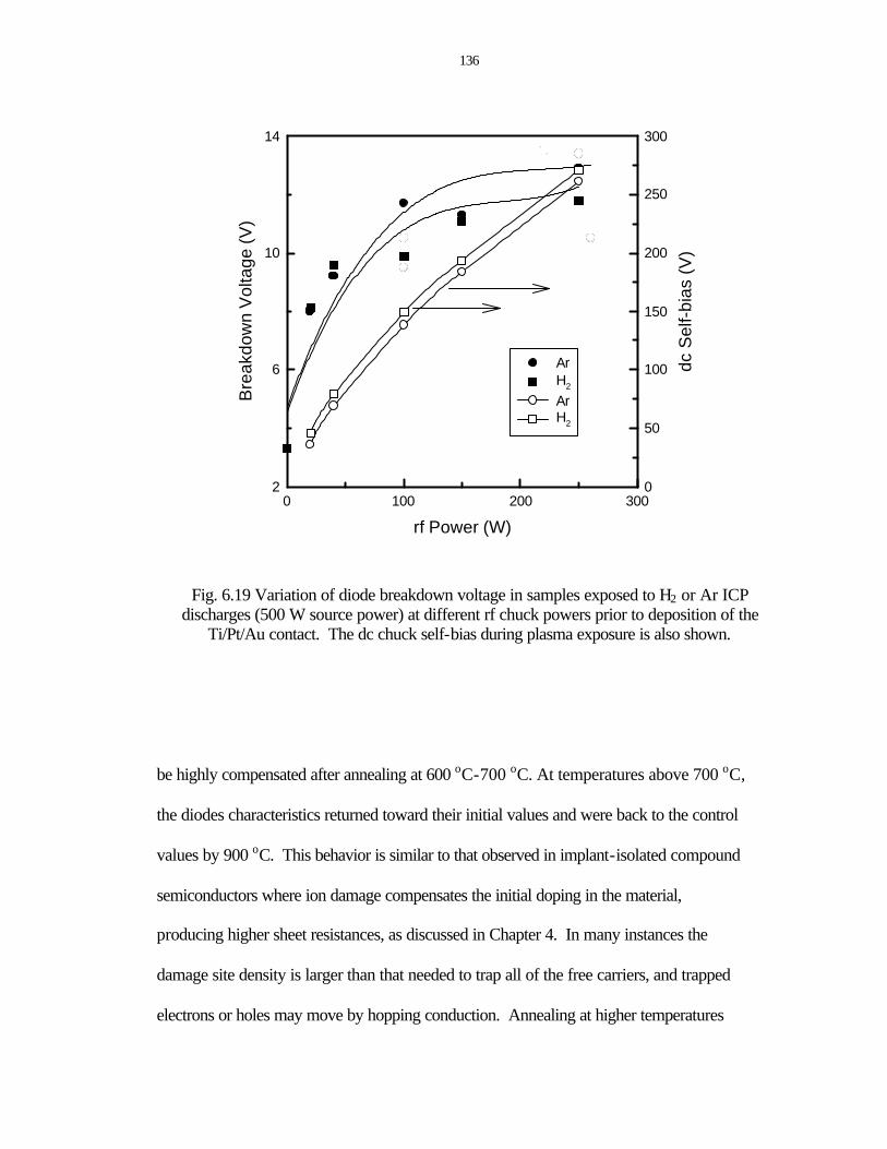
136
Fig. 6.19 Variation of diode breakdown voltage in samples exposed to H2 or Ar ICP discharges (500 W source power) at different rf chuck powers prior to deposition of the
Ti/Pt/Au contact. The dc chuck self-bias during plasma exposure is also shown.
be highly compensated after annealing at 600 oC-700 oC. At temperatures above 700 oC,
the diodes characteristics returned toward their initial values and were back to the control
values by 900 oC. This behavior is similar to that observed in implant-isolated compound
semiconductors where ion damage compensates the initial doping in the material,
producing higher sheet resistances, as discussed in Chapter 4. In many instances the
damage site density is larger than that needed to trap all of the free carriers, and trapped
electrons or holes may move by hopping conduction. Annealing at higher temperatures
rf Power (W)
0 100 200 300
Bre
akdo
wn
Vol
tage
(V
)
2
6
10
14
dc S
elf-
bias
(V
)
0
50
100
150
200
250
300
ArH2
ArH2

137
removes some of the damage sites, but there are still enough to trap all the conduction
electrons/holes. Under these conditions the hopping conduction is reduced and the
sample sheet resistance actually increases. At still higher annealing temperatures, the
trap density falls below the conduction electron or hole concentration and the latter are
returned to their respective bands. Under these conditions the sample sheet resistance
returns to its pre-implanted value. The difference in the plasma exposed samples is that
the incident ion energy is a few hundred eV compared to a few hundred keV in implant-
isolated material. In the former case the main electrically active defects produced are
nitrogen vacancies near the surface, whereas in the latter case there will be vacancy and
interstitial complexes produced in far greater numbers to far greater depths. We did not
examine the time dependence of the damage removal, but expect it would show a square
root power of annealing time.
In our previous work on plasma damage in n-GaN we found that annealing at ~750
oC almost returned the electrical properties to their initial values. If the same defects are
present in both n- and p-type materials after plasma exposure, this difference in annealing
temperature may be a result of a Fermi level dependence to the annealing mechanism.
6.4 Determination of Damage Profile in GaN
An important question is the depth of the plasma-induced damage. We found we
were able to etch p-GaN very slowly in boiling NaOH solutions, at rates that depended on
the solution molarity (Fig. 6.21) even without any plasma exposure of the material. This
enabled us to directly measure the damage depth in plasma exposed samples in two
different ways.
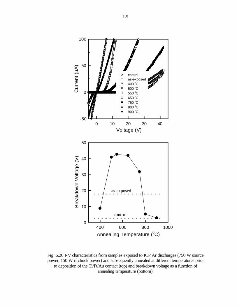
138
Fig. 6.20 I-V characteristics from samples exposed to ICP Ar discharges (750 W source power, 150 W rf chuck power) and subsequently annealed at different temperatures prior
to deposition of the Ti/Pt/Au contact (top) and breakdown voltage as a function of annealing temperature (bottom).
Voltage (V)0 10 20 30 40
Cur
rent
(µ
A)
-50
0
50
100
controlas-exposed400 oC500 oC550 oC650 oC750 oC800 oC900 oC
Annealing Temperature (oC)
400 600 800 1000
Bre
akdo
wn
Vol
tage
(V
)
0
10
20
30
40
50
as-exposed
control

139
Fig. 6.21 Wet etching rate of p-GaN in boiling NaOH solutions as a function of solution
molarity.
The first method involved measuring the etch rate as a function of depth from the
surface. Defective GaN resulting from plasma, thermal or implant damage can be wet
chemically etched at rates much faster than undamaged material because the acid or base
solutions are able to attack the broken or strained bonds present. Kim et al.129 reported
that the wet etch depth on thermally or ion-damaged GaN was self-limiting. Fig. 6.22
shows the GaN etch rate as a function of depth in samples exposed to a 750 W source
power, 150 W rf chuck power Ar discharges (-158 V dc bias). The etch rate is a strong
function of the depth from the surface and saturates between ~425-550 Å. Within this
depth range the etch rate is returned to the “bulk” value characteristic of undamaged p-
GaN.
Solution molarity (M)
0.1 1
Etc
hing
Rat
e (Å
/min
)
10
15
20
25
30
35
p-GaN in Boiling NaOH

140
Fig. 6.22 Wet etching rate of Ar plasma-exposed (750 W source power, 150 W rf chuck
power) p-GaN as a function of depth into the sample.
The second method to establish damage depth of course is simply to measure the I-
V characteristics after removing different amounts of material by wet etching prior to
deposition of the rectifying contact. Figure 6.23 (top) shows the I-V characteristics from
samples exposed to 750 W source power, 150 W rf chuck power (-160 V dc chuck bias)
Ar discharges and subsequently wet etched to different depths using 0.1 M NaOH
solutions before deposition of the Ti/Pt/Au contact. Fig. 6.23 (bottom) shows the effect
of the amount of material removed on the diode breakdown voltage. Within the
Depth (Å)
0 200 400 600
Etc
hing
Rat
e (Å
/min
)
101
102
103
104
Ar plasma-exposed p-GaNin boiling 0.1 M NaOH

141
experimental error of ± 12%, the initial breakdown voltage is re-established in the range
400-450 Å. This is consistent with the depth obtaine d from the etch rate experiments
described above, and corresponds to the ion energy of ~180 eV.
It would be instructive to determine and compare the damage depth created after
exposure to Cl2/Ar and Ar discharges (500 W source power, 150 W rf chuck power, 1
min, –192 V or –171 V dc chuck bias). For these plasma conditions, we did not observe
type conversion of the surface. The values of forward turn-on voltage increased after
plasma exposure, due to the lowered net hole concentration. The electrical properties are
almost restored after depths of 500-600 Å were removed by NaOH etching, as can be
seen in Fig. 6.24. This data can also be obtained from Fig. 6.25, where the wet etch depth
in plasma damaged p-GaN is plot as a function of etching time. What is clear from this
data is the damage depth produced in Cl2/Ar discharges is only slightly smaller than that
in Ar discharges, even though the etch rate of GaN in the former plasma is almost 30
times higher.
The damage depth in n-type GaN can be established by photoelectrochemically
(PEC)130 wet etching different amounts of the plasma-exposed material, and then
measuring the electrical properties of the GaN surfaces. For samples exposed to a 500 W
source power, 150 W rf chuck power N2 discharge, the reverse breakdown voltage was
restored to about half of its initial value after removal of ~260 Å damaged layer.
However, increasingly rough surfaces of PEC etching for larger removal depths were
usually observed. The estimated damage depth for the N2 plasma conditions mentioned
above could be similar with that established in p-type GaN samples exposed to similar
plasma conditions.

142
Fig. 6.23 I-V characteristics from samples exposed to ICP Ar discharges (750 W source power, 150 W rf chuck power) and subsequently wet etched to different depths prior to deposition of the Ti/Pt/Au contact (top) and breakdown voltage as a function of depth
removed (bottom).
Voltage (V)-10 0 10 20 30
Cur
rent
(µ
A)
-50
0
50
100
controlas-exposed150 Å300 Å400 Å600 Å
Depth Removed (Å) 0 100 200 300 400 500 600 700
Bre
akdo
wn
Vol
tage
(V
)
0
4
8
12
16
20
control
as-exposed

143
Fig. 6.24 Forward I-V characteristics from p-GaN samples exposed to ICP Cl2/Ar (top) or Ar (bottom) discharges (500 W source power, 150 W rf chuck power) and wet etched in
boiling NaOH to different depths prior to deposition of the rectifying contact.
Voltage (V)
-8 -6 -4 -2 0
Cur
rent
(m
A)
-0.6
-0.4
-0.2
0.0
control400 Å500 Å600 Å
Ar150 W rf500 W ICP
Voltage (V)-8 -6 -4 -2 0
Cur
rent
(m
A)
-0.6
-0.4
-0.2
0.0
control400 Å500 Å550 Å
Ar/Cl2
150 W rf500 W ICP

144
Fig. 6.25 Wet etch depth versus etch time in boiling NaOH solutions for plasma damaged p-GaN.
Etching Time (s)101 102 103
Etc
h D
epth
(Å
)
102
103
Ar exposedAr/Cl2 etched
p-GaN 0.1 M boiling NaOH

1
CHAPTER 7 FABRICATION AND SIMULATION OF GaN-BASED BIPOLAR TRANSISTORS
7.1 Introduction
Wide band gap materials such as III-V nitrides and SiC enjoy the associated
advantages of low intrinsic carrier concentration and high breakdown field, and have
proven to be effective for electronics for high temperature (>400 oC) and high power
(>100 W) applications.4 The recent progress in field effect AlGaN/GaN transistors has
been impressive, and has demonstrated record figures of high power microwave
performance.38-41 Compared to unipolar transistors, HBTs have higher current-carrying
capacity, more uniform threshold voltages and better linearity, which are particularly
important for radar and communications applications. The driving forces behind the
current AlGaN/GaN HBT research come from the inherent promises of this type of
device as well as the recent success of AlGaN/GaN heterostructure in both
optoelectronics and microelectronics.36,39 However, timely development has been
hampered by difficulties with growth of high quality junctions and p-type doping. High
base doping concentration is required to achieve low output conductance. In state-of-the-
art p-type GaN, the acceptor Mg concentration is usually two orders of magnitude higher
than the hole concentration due to the high ionization level, while incorporation of high
density of dopants can significantly reduce minority carrier lifetime and mobility in the
base region. The few reports on GaN/AlGaN HBTs fabricated to date have shown

146
performance limited by high base recombination rate and high base resistance, with
current gain of ~3 at room temperature.49,50 Moreover the epitaxial growth processes for
these devices are far from perfected and the material quality is compromised because of
the high defect densities in currently-employed heteroepitaxial crystals. Especially in the
MBE grown device structures, junction leakage remains one of the key issues to be
solved.
Compared to FETs, the vertical device structures with buried p-type GaN layer,
such as npn HBTs and thyristors, put much more demand on fabrication techniques. The
challenging issues include how to remove plasma damage and make low resistance ohmic
contact after dry etching down to the p-type base region. Damage on the sidewall may
result in large leakage current, and must be annealed. N2 loss from the surface and
impurity interdiffusion at the interfaces during the thermal processes may degrade the
device performance. In addition, good quality ohmic contacts are difficult to be achieved
even on n-type regions, because the annealing temperature cannot go high after metal is
deposited on the multilayer structures.
All the work on processing discussed in earlier chapters is directed towards the
optimization of GaN-based device performance. In this chapter, MBE grown GaN BJTs
and AlGaN/GaN HBTs have been demonstrated with the technical improvements such as
low damage dry etch, damage removal, and better ohmic contacts. The devices worked at
high temperatures and high powers in common-base mode. The issues related to growth
and fabrication which remain unsolved were addressed. Finally, quasi-3D simulation of
the bipolar transistors (both npn and pnp structures) was performed by using a physically-

147
based simulator ATLAS/BLAZE. The effect of layer structure design and materials
parameters on the dc performance of the devices were calculated.
7.2 Common Base Operation of GaN BJT and HBT
The layer structures of the devices, as shown in Fig. 7.1, were grown by Molecular
Beam Epitaxy using rf plasma activated N2 and solid Ga and Al. Since we have
previously found that the breakdown and leakage characteristics of GaN devices are
Fig. 7.1 Layer structure for HBT and BJT.
HBT Design
GaN 5000 Å 1×1019 cm-3 n
AlGaN to GaN, 200 Å 1×1019 cm-3 n
AlGaN 20% 800 Å, 1×1019 cm-3 n
AlGaN 5% 200 Å, UID
AlGaN x=0 to 5%, 2000 Å, p+
GaN 4000 Å 5×1016 cm-3 n
GaN 5000 Å 8×1016 cm-3 n
BJT Design
GaN 5000 Å 1×1019 cm-3 n
GaN 200 Å UID
GaN 2000 Å p+
GaN 4000 Å 5×1016 cm-3 n
GaN 5000 Å 8×1018 cm-3 n
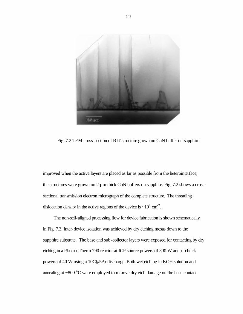
148
Fig. 7.2 TEM cross-section of BJT structure grown on GaN buffer on sapphire.
improved when the active layers are placed as far as possible from the heterointerface,
the structures were grown on 2 µm thick GaN buffers on sapphire. Fig. 7.2 shows a cross-
sectional transmission electron micrograph of the complete structure. The threading
dislocation density in the active regions of the device is ~109 cm-2.
The non-self-aligned processing flow for device fabrication is shown schematically
in Fig. 7.3. Inter-device isolation was achieved by dry etching mesas down to the
sapphire substrate. The base and sub-collector layers were exposed for contacting by dry
etching in a Plasma-Therm 790 reactor at ICP source powers of 300 W and rf chuck
powers of 40 W using a 10Cl2/5Ar discharge. Both wet etching in KOH solution and
annealing at ~800 oC were employed to remove dry etch damage on the base contact

149
Fig. 7.3 Schematic of process sequence for GaN/AlGaN HBT.
(b) Base Mesa Etching
(a) Emitter Mesa Etching
(d) Base Metal Contact
(c) Emitter/Collector Metallization
(e) Device Isolation
PR
PR

150
region and the mesa sidewall. N-type ohmic metallization of Ti/Al/Pt/Au and p-type
metallization of Ni/Au were deposited by e-beam evaporation and patterned by lift-off.
The contacts were annealed at 500 oC for 30 secs under a N2 ambient to reduce the
contact resistance. Fig. 7.4 shows a SEM of a completed HBT (top), together with
devices with emitter diameters of 50-90 µm (bottom). The devices were tested at
temperatures up to 300 oC using a temperature-controlled probe station and an HP 4145A
parameter analyzer.
Fig. 7.4 SEM micrograph of complete HBTs.

151
Common-base current-voltage characteristics from a 90 µm diameter HBT are
shown in Fig. 7.5. The collector-base breakdown voltage VBCB is ~10 V at 25 oC (top),
with an onset of IC of 2-3 V, which is close to the built-in potential of the junction. The
saturated collector current is nearly equal to the emitter current, indicating a high emitter
injection efficiency. At 250 oC the common-base breakdown voltage (VBCB) decreased to
~4 V, as shown at the bottom of Fig. 7.5. The negative temperature coefficient for VBCB
may be due to defect-assisted tunneling currents, either from bulk or surface states. Large
junction leakage is currently a problem, especially for MBE growth. At both 25 oC and
250 oC the junction ideality factors for both emitter-base and collector-base junctions
were close to 2, indicative of significant recombination. Another area for future research
will be methods for surface passivation of these device structures.
Gummel plots showed dc current gains of 15-20 at room temperatures (Fig. 7.6),
which is a significant improvement over past results. The oscillations at low bias in IC
are due to incomplete shielding of the test set-up. By removing the base contact, we
observed much smaller collector current, which confirms the transistor modulation. In
most of the devices we could not obtain common-emitter operation due to leakage in the
collector-base junction, and high base series resistance. P-type doping must be improved
to lower the resistance in the extrinsic and intrinsic base regions. Better base contact is
also required. At this point, this can be achieved by using thick contact region (extrinsic
base regrowth).
Since the main applications for GaN/AlGaN HBTs relate to their current-carrying
capability, it is of interest to measure the current density. Fig. 7.7 shows common-base
characteristics from a 50 µm diameter emitter device at 25 oC. The current density was

152
Fig. 7.5 Common-base characteristics from 50 µm diameter devices at 25 oC (top) and 250 oC (bottom). The emitter current was stepped in 200 µA increments from 200 µA.
VCB (V)-4 0 4 8 12
Cur
rent
(m
A)
0.0
1.0
2.0
3.0
25 oC
IE = 200 µA/div
GaN/AlGaN HBT
VCB (V)-4 0 4 8 12
Cur
rent
(m
A)
0.0
1.0
2.0
3.0
250 oC

153
Fig. 7.6 Gummel plot of GaN/AlGaN HBT at 25 oC.
2.55 kA·cm-2 at 8 V, corresponding to a power density of 20.4 kW·cm-2. We note that our
devices are not optimized for power operation at this point. With optimized device and
use of a power mask-set, much higher powers could be expected. This is the first report
of power densities in GaN/AlGaN HBTs, showing the potential of these devices for
microwave power amplifiers. At high temperatures, the breakdown voltage decreased,
and hence the maximum power density obtained was lower.
VB (V)
0 4 8 12
Cur
rent
(A
)
10-9
10-8
10-7
10-6
10-5
10-4
Gai
n
0.01
0.1
1
10
100
Ic
Ib

154
Fig.7.7 Common-base characteristics of GaN/AlGaN HBT at 25 oC.
Common-base I-V characteristics for the GaN BJTs are shown in Fig. 7.8 for both
25 oC and 300 oC measurement temperatures. The saturated collector current is nearly
equal to the emitter current. At 300 oC, the devices turn-on at lower collector-base
voltages but the breakdown voltage is lower. We obtained a maximum current density of
3.6 kA·cm-2 for 50 µm diameter devices at 15 V, corresponding to a power density of 54
kW·cm-2. The offset voltage is relatively high and is probably related to the high base
contact resistance. The maximum common-emitter dc current gain
B
C
dIdI was ~15 at
VCB (V)
-4 0 4 8 12
Cur
rent
(A
)
-0.02
0.00
0.02
0.04
0.06
0.08
IE = 10 mA
GaN/AlGaN HBTemitter area: 1.96 x 10⁻⁵ cm2
J = 2550 A/cm-2

155
both temperatures, as obtained from Gummel plots. Improved junction properties and
possibly surface passivation methods are likely to lead to better device performance. The
forward I-V characteristics of the junctions showed evidence of significant
recombination. Again, the reduced breakdown voltage at 300 oC may be due to defect-
related leakage. For our designs, the BJTs appeared to be more powerful and thermally
stable than the HBTs. This can probably be related to the better structure quality. The
AlGaN/GaN HBT is relatively more complicated to grow, and the incorporation of Al
could result in high density of defects at the hetero-interface.
Fig. 7.8 Common-base characteristics of 50 µm diameter BJT at 25 oC and 300 oC. Emitter current was stepped from 10 to 70 mA in 10 mA steps.
VCB (V)
-4 0 4 8 12
Cur
rent
(A
)
0.00
0.02
0.04
0.06
0.08
0.10
0.12
25 oC300 oC

156
A noticeable effect is that the offset voltage is relatively high in the BJTs and
increases with the measurement current levels as illustrated in detail in Fig. 7.9, which
shows common-base characteristics as a function of the magnitude of the emitter current
steps (10 µA-10 mA). The increases in offset voltage at higher current levels may be a
result of the high base contact resistance, as well as the fact that higher voltages are
needed to reach a particular current level.
7.3 Growth and Processing Issues
Several key issues, related to interface quality, impurity and doping control,
minority carrier lifetime and base doping and contact, remain to be resolved for III-V
nitride HBTs to achieve good common-emitter operation and AC performance. First
among these is how to suppress the junction leakage in the MBE grown structure. It has
been firmly established that the quality of the epi layers is a function of growth thickness
and the type of buffer layer on which they are grown. Fig. 7.10 shows I-V characteristics
from the emitter-collector junction for devices grown by MBE directly on sapphire, or on
buffers grown by MOCVD or HVPE. While the latter are much thicker (>10 µm), the
morphology can be much rougher than MOCVD buffers. It is quite evident the junction
quality is significantly improved on the MOCVD buffers. The dislocation density in the
active regions is reduced by at least one order of magnitude, as revealed by TEM
measurements.
The second concern is achieving good dopant and background impurity control in
HBT structures. The p-type dopant should be rapidly switched on and off around the base
region, and not spill-over into the adjacent n-type AlGaN emitter, where it could cause

157
Fig. 7.9 Common-base characteristics of BJTs at 25 oC as a function of different emitter current increments.
-4 0 4 8 12 16
Cur
rent
(A
)
0.00000
0.00004
0.00008
0.00012
0.00016
0.00020
IE = 10 µA/step
G aN -B JT
-4 0 4 8 12 16
Cur
rent
(A
)
0.0000
0.0004
0.0008
0.0012
0.0016
0.0020
IE = 200 µA/step
VCB (V)
-4 0 4 8 12 16 20
Cur
rent
(A
)
0.00
0.02
0.04
0.06
0.08
IE = 10 mA/step

158
Fig. 7.10 I-V characteristics measured between emitter and collector for HBTs grown on different GaN buffers on sapphire substrates.
displacement of the junction and hence the loss of the advantage of the heterostructure.
Fig. 7.11 shows SIMS profiles of the Al marker (open circle), signifying the position of
AlGaN emitter layer, and also the Mg doping profile (solid circle) in the adjacent base
region. The base layer is well defined. The so-called “memory effect” associated with the
use of Mg131 is illustrated by the appearance of a spike-like feature in the Mg profile after
the Mg has been switched off. We note that growth rate for the n-AlGaN is much lower
Voltage (V)
-20 -10 0 10 20
Cur
rent
(m
A)
-0.1
0.0
0.0
on sapphireon HVPE-GaNon MOCVD-GaN
EC junction

159
than that for the p-GaN base (~1 µm/hr), this would explain the observed enhancement
(or spiking) of Mg incorporation during the initial base-emitter transition. It is clear that
the reactor memory effect has produced incorporation of Mg in the emitter, although the
real situation is not quite as severe as it seems in the data because of “carry-over” of the
matrix Al signal during the depth profiling. The fact that HBT characteristics can still be
obtained on this material means there is a net surplus of donor over acceptors, and not all
of the Mg can be electrically active in the AlGaN. Both the emitter and emitter-contact
layers remain n-type.
Fig. 7.11 SIMS profile of Mg in MBE grown GaN/AlGaN HBT structures.
Depth (microns)
0.0 0.2 0.4 0.6
Con
cent
ratio
n (a
tom
s/cc
)
1017
1018
1019
1020
1021
Sec
onda
ry Io
n C
ount
s
102
103
104
105
106
Mg
Al
MBEGaN/AlGaN HBT

160
Another aspect of impurity control is to minimize the concentration of O (which
probably creates a shallow donor state in GaN), C (which may lead to compensated
material) and H (which can passivate the Mg acceptors in the base). In MBE grown
samples, we usually observe the concentrations of C and O throughout most of the
structure are well below that of the intentionally doped Si, suggesting it will have no
significant effect on the electrical properties of the material. The incorporation of H is
also low, and this is in a contrast to the MOCVD growth, where high concentration
residual hydrogen decorates the Mg doping in the base, as shown in Fig. 7.12. This is the
case even after the in situ activation anneal standard for all MOCVD-grown GaN device
structures containing p-layers. We assume in analogy with the behavior of H in other
compound semiconductor systems that this anneal dissociates the (Mg-H)o neutral
complexes, producing Mg- acceptors and inactive H2 molecules. Thus, while the
hydrogen is still present at a significant concentration in the base, it is not in an active
form, and does not effect the electrical properties. It remains to be established as to the
relative contributions of background impurities and structural defects to degradation of
gain in GaN/AlGaN HBTs.
High specific contact resistance (in particular the p-ohmic contact) is a limiting
factor in GaN-based device performance. Fig. 7.13 shows the alloying temperature
dependence of the I-V characteristics for Ni/Au contacts to the p-type base layer.
Annealing at progressively higher temperatures produced a significant improvement, but
the contacts were clearly not purely ohmic and better described as a leaky Schottky
contacts. It is noteworthy that 600 oC is the highest annealing temperature can be used in

161
Fig. 7.12 SIMS profiles showing H decorating the base region in an MOCVD grown GaN/AlGaN HBT structure.
Fig. 7.13 Annealing temperature dependence of I-V characteristics for Ni/Au on the p-type base layer.
Depth (microns)
0 1 2 3
Con
cent
ratio
n (a
tom
s/cc
)
1017
1018
1019
1020
1021
1022
Sec
onda
ry Io
n C
ount
s
100
101
102
103
104
105
H
Al
Si
O
C
MOCVD GaN/AlGaN HBT
Voltage (V)
-2 0 2
Cur
rent
(mA
)
-0.04
-0.02
0.00
0.02
0.04
as-deposited500 oC annealed600 oC

162
most device structures due to junction shorting. In addition, the high sheet resistance in
the base due to poor p-type doping could also result in significant parasitic loss,
especially when the base layer is thin. Fig. 7.14 shows the typical I-V characteristics at 25
oC and 250 oC from the base-collector and base-emitter junctions of BJTs. Note that
there is a kink in the I-V trace for the base-collector junction at ~3.2 V indicating the
presence of forward injection current. However, for the base-emitter junction, the forward
onset voltage is too high for a pn junction with a built-in potential ~3.2 V indicating high
on-resistance. In the former case, the current flows straight down from base contact to
collector (similar as in the commercialized GaN LED structure), and the voltage drop on
the thin base region is small. However in the latter case, current flows laterally in the
base, both high bulk resistivity and current crowding effect limit the carrier transport. The
current increases at higher temperatures due to improved thermionic emission as well as
higher ionization efficiency of acceptors in the intrinsic and extrinsic base regions.
Regrowth of base contact region or self-aligned base-emitter junction can reduce
the extrinsic and intrinsic base resistance, while the key issue is to improve the material
quality and p-type doping. Invoking a piezoelectric field to induce free holes in the base
is one of potential solutions.132
Minority carrier lifetime is a critical parameter in the gain of bipolar transistors and
the conductivity modulation of thyristors. It is also a critical measurement of material
quality as it relates to traps and recombination centers. The minority hole lifetime in
state-of-the-art n-GaN has been measured to be on the order of 2-7 ns, and the electron
lifetime in p-GaN is about one or two orders lower.133,134 Bandic et al.134 found that line
dislocations in unintentionally doped GaN act as recombination sites, and limit the

163
minority carrier transport properties. As the crystalline quality is improved, better values
of the minority carrier lifetime in GaN can be expected.
Fig. 7.14 I-V characteristics of base-collector and base-emitter junctions in BJTs at 25 oC or 250 oC.
Voltage (V)
0 2 4 6 8
Cur
rent
(A
)
10-9
10-8
10-7
10-6
10-5
10-4
10-3 BJT BC
BE
25 oC250 oC
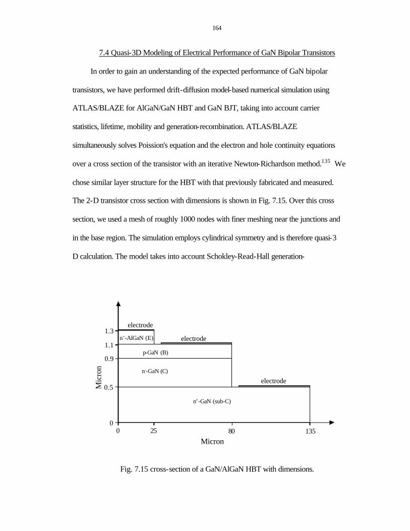
164
7.4 Quasi-3D Modeling of Electrical Performance of GaN Bipolar Transistors
In order to gain an understanding of the expected performance of GaN bipolar
transistors, we have performed drift-diffusion model-based numerical simulation using
ATLAS/BLAZE for AlGaN/GaN HBT and GaN BJT, taking into account carrier
statistics, lifetime, mobility and generation-recombination. ATLAS/BLAZE
simultaneously solves Poission's equation and the electron and hole continuity equations
over a cross section of the transistor with an iterative Newton-Richardson method.135 We
chose similar layer structure for the HBT with that previously fabricated and measured.
The 2-D transistor cross section with dimensions is shown in Fig. 7.15. Over this cross
section, we used a mesh of roughly 1000 nodes with finer meshing near the junctions and
in the base region. The simulation employs cylindrical symmetry and is therefore quasi-3
D calculation. The model takes into account Schokley-Read-Hall generation-
Fig. 7.15 cross-section of a GaN/AlGaN HBT with dimensions.
0 25 80 1350
0.5
0.9
1.1
1.3
Micron
Mic
ron
n+-AlGaN (E)
p-GaN (B)
n+-GaN (sub-C)
electrode
electrode
electroden--GaN (C)

165
recombination, Auger and optical processes, concentration dependent low field mobility
and lifetime, parallel electric field-dependent mobility, Selberherr's impact ionization and
Fermi-Dirac statistics. For high temperature performance, we took into account the
temperature dependence of carrier low-field mobility and material bandgap. A list of the
parameters employed is shown in Table 7.1 for hexagonal GaN and Al0.2Ga0.8N.136
Table 7.1 Parameters used in the simulations. Eg (GaN) = 3.4 eV (300 K) Nc (GaN) = 2.24×10⁻¹⁸ cm-3 Vv (GaN) = 1.8×1019 cm-3 εs (GaN) = 8.9 νsn (GaN) = 2.5×107 cm·s-1 νsp (GaN) = 106 cm·s-1 Epeak (GaN) = 1.4×10⁵ V·cm-1 Richardson constant (GaN) Ae* = 26.4 A·cm-2·K-2 Ap
* = 96 A·cm·-2·K-2 Auger Recombination Coefficients Aug(n) = 10-30 cm6·s-1
Aug(p) = 10-31 cm6·s-1
GaN/AlGaN band offset ratio Qc = 0.7 Temperature dependence of bandgap
( ) ( )
Kwhere
TT
ETE gg
700
300300
2032.730022
4
=
+
−+
×+= −
β
ββ
Low field mobility
5.1
7.1
300
300−
−
=
=
T
T
ppo
nno
µµ
µµ
Impact ionization (Sellaherr’s model): parameters for SiC Parameters for AlGaN: GaNAlNAl NGa χχχ 8.02.0
8.02.0+=

166
7.4.1 npn Structure
A typical device structure and doping for the npn HBT are shown in Table 7.2.
Since the Mg dopant for the base has a large ionization energy (170 meV), an acceptor
concentration approximately an order of magnitude higher than the required hole density
is necessary. The material quality is still compromised in currently available GaN due to
the high defect concentrations and impurity backgrounds. For this reason we took both
the best and typical values for carrier mobility and lifetime in each of the different layers
(which have different doping levels), and assumed there was little difference between the
values for majority and minority carriers. These range of values are listed in Table 7.3.
Table 7.2 npn GaN/AlGaN HBT structure and doping.
material thickness (Å) doping (cm-3)
emitter n+-AlGaN 2000 1×10¹⁹
base p-GaN 2000 2×10¹⁷
collector n--GaN 4000 5×10¹⁶
subcollector n+-GaN 5000 8×10¹⁸
Table 7.3 Best and typical values of mobility and lifetime in each layer of the HBT.
µe/µh τe/τh
optimistic typical optimistic typical
emitter 40/5 20/2 1×10-11/1×10-10 1×10-11/5×10-11
base 600/30 300/14 2×10⁻¹⁰/7×10-9 8×10-11/4×10-9
collector 800/40 450/22 1×10⁻⁹/2×10-8 5×10⁻¹⁰/1×10-8
subcollector 200/10 80/4 1×10-11/2×10-10 1×10-11/1×10-10

167
For the layer structure of Table 7.2, the predicted Gummel plots for the HBT are
shown at the top of Fig. 7.16 for both the optimistic and typical values of carrier mobility
and lifetime. Note that the turn-on voltage is ~2.5 V in both cases. The corresponding dc
current gains are shown at the bottom of Fig. 7.16, as a function of collector current in
devices with 50 µm diameter circular contacts. It is clear that the materials quality can
have a tremendous impact on the gain of the device. In the ideal operation region, the
gain is ~30 for high quality material, but <10 for more typical structures. Note that even
with the best parameters, the calculated gain is limited, probably by the recombination in
the base. At high injection levels, the base spreading resistance could result in non-
uniform distribution of the emitter current called emitter current crowding. We observed
most of the emitter current was concentrated near the edges of the emitter-base junction
at current densities >103 A⋅cm-2. Correspondingly, high recombination rates >5×1025 cm-2
were confined in a small region in the base at the periphery of the junction.
Additional improvements in dc current gain can be obtained by grading the base
layer. In Fig. 7.17 we show the results of grading this layer from GaN to Al0.12Ga0.88N
linearly, relative to layer of constant compositions. We assumed the optimum values for
carrier lifetime and mobility and considered that the transport properties in AlGaN are
usually much worse than in GaN. Note that the current gain can reach almost 100 for the
graded structure at high current density, at the expense of a slight increase in turn-on
voltage. The electron transit time is decreased in the graded structure due to the presence
of a quasi-electric field directed from the collector-base junction towards the emitter-base
junction (of ~17 kV·cm-1). In this case, the electrons are transported across the base by
diffusion as well as drift.

168
Fig. 7.16 Gummel plot (top) and dc current gain (bottom) for the HBT with structure of Table 7.1, assuming either optimistic or typical values for carrier mobility and lifetime.
VBE (V)
2 3 4 5
Cur
rent
(A
)
10-13
10-12
10-11
10-10
10-9
10-8
10-7
10-6
10-5
10-4
10-3
10-2
10-1
IBICIBIC
typical
optimistic
npn HBT
Collector Current (A)
10-12 10-11 10-10 10-9 10-8 10-7 10-6 10-5 10-4 10-3 10-2
Cu
rre
nt G
ain
1
10
100
optimistictypical

169
Fig. 7.17 Gummel plot (top) and dc current gain (bottom) for the HBT with structure of Table 7.1, with either a graded or constant composition base layer.
VBE (V)
2 3 4 5
Cur
rent
(A)
10-12
10-11
10-10
10-9
10-8
10-7
10-6
10-5
10-4
10-3
10-2
10-1
IB
ICIBIC
graded
flat
Collector Current (A)
10-12 10-11 10-10 10-9 10-8 10-7 10-6 10-5 10-4 10-3 10-2
Cur
rent
Gai
n
1
10
100
flatgraded

170
Fig. 7.18 shows the effect on dc current gain of these parameters, namely base
thickness (top), minority carrier mobility in the base (center) and minority carrier lifetime
in the base (bottom). As expected the gain decreases as the base thickness is increased,
due to increased recombination of electrons. Note that with high quality material and a
base thickness of 1000 Å, gains of several hundred are possible. There is a direct
correlation of gain with the minority carrier mobility, due to the reduced transit time
through the base and hence lower recombination, while minority carrier lifetime also has
a very strong influence on the device performance. Since GaN is a direct gap material, its
minority carrier lifetime would be small. The gain is maximized at low base doping
levels in high quality material. When recombination current dominates, we can
approximate the common emitter current gain β , as76
β ≈T
eτ
τ (7.1)
where τe is the electron lifetime in the base and τT is the transit time proportional to
µ⋅
ekT
WB2
eB. Note that in an ideal HBT, the gain is limited by emitter injection
efficiency, and given by:76
)/exp( kTENN
abpe
denbυυ
υβ ∆= (7.2)
where υnb and υpe are effective velocities of electrons in the base and holes in the emitter,
Nde and Nab are doping concentration in the emitter and the base, and ∆Ev is the valence-
band offset at the hetero-interface.
Fig. 7.19 shows calculated common-emitter characteristics for a base doping (hole
concentration) of 2×1017 cm-3 (top), in which the gain is >20 and the Early voltage is ~3

171
Fig.7.18 Effect on dc current gain of base thickness (top), electron mobility in base (center) or electron lifetime in base (bottom).
Base Thickness (Å)
1000 2000 3000 4000
Gai
n1
10
100
optimistictypical
Minority Carrier Lifetime in Base (s)
10-11 10-10 10-9
Gai
n
100
200
300
optimistictypical
Minority Carrier mobility in Base (cm2/V·s)
0 2x10² 4x10² 6x10² 8x10²
Gai
n
20
40
60
80
100
optimistictypical

172
Fig. 7.19 Common-emitter characteristics for the HBT with structure of Table 7.1, for hole concentrations of 2×1017 cm-3 (top) or 1018 cm-3 (bottom) in the base.
VCE (V)
0 2 4 6
I C (
A)
0.0000
0.0001
0.0002
0.0003
Base doping 2x1017 cm-3
IB=1 µA/step
VCE (V)
0 2 4 6
I C (A
)
Base doping 1x1018 cm -3
IB=1 µA/step
0
2x10⁻⁵
4x10⁻⁵

173
V, and for a hole concentration in the base of 1018 cm-3 (bottom), in which the gain is ~5
and the Early voltage becomes much larger because it is proportional to QG, the Gummel
number. The characteristics do not show good saturation behavior for low base doping
due to the base push-out effect.
The relatively high base contact specific resistance is a problem for npn GaN
transistors and leads to ohmic heating of the contact/semiconductor interface. This in turn
severely degrades the reliability of the device. The typical values of the contact resistance
on p-GaN are in the 10-2 to 10-3 Ω⋅cm2 range, but it could be much worse in practical
device because high temperature annealing is not applicable. Fig. 7.20 shows the effect of
the base contact specific resistance on the Gummel plots from devices with optimum
carrier lifetime and mobility. The case of a high base resistance reduces the gain at high
current and reduces the low-bias current, emphasizing how important the base contact is
in influencing device performance.
The effect of elevated temperature on the Gummel plots is shown in Fig. 7.21 (top).
At high temperatures the turn-on decreases, however the gain decreases somewhat due to
lower carrier mobility. In the open-base state, the punch-through breakdown voltage
BVCEO also decreases from ~18 V to ~14 V, as shown at the bottom of Fig. 7.21.
However, the device operation is still quite good at 300 oC, and shows the promise of this
technology for elevated temperature operation.
Fig. 7.22 shows a comparison of the expected gain for HBT and BJT structures with
the same doping and layer thickness. Despite the high band-offset ratio of the
AlGaN/GaN heterojunction (Qc~0.7, a high conduction-band spike forms at the hetero-
interface which necessitates thermionic emission and tunneling for electron transport

174
from the n-to-p quasineutral regions), the HBT enjoys a significant advantage in the low
injection regime. The results converge at high current densities, and under these
conditions the BJT is an attractive alternative because it is simpler to grow.
Fig. 7.20 Effect of base contact resistance on Gummel plots.
VBE (V)
2 3 4 5
Cur
rent
(A
)
10-13
10-12
10-11
10-10
10-9
10-8
10-7
10-6
10-5
10-4
10-3
10-2
10-1
IBICIBIC
Rc=0.1 Ω·cm2
Rc=0

175
Fig. 7.21 Effect of device operating temperature on Gummel plot (top) or the breakdown voltage of the C-E junction (bottom).
VBE (V)
1 2 3 4 5
Cur
rent
(A
)
10-13
10-12
10-11
10-10
10-9
10-8
10-7
10-6
10-5
10-4
10-3
10-2
10-1
IBICIBIC
300 oC
RT
VCE (V)
0 4 8 12 16 20
Col
lect
or C
urre
nt (
A)
0e+0
4e-6
8e-6
1e-5
2e-5
2e-5
RT300 oC

176
Fig. 7.22 Current gain as a function of collector current for HBT and BJT of the same
layer thicknesses and doping.
7.4.2 pnp Structure
One of the limiting factors for npn devices was the high sheet resistance of the base,
which results from the large ionization energy of the Mg acceptors in GaN (~170 meV).
An obvious alternative is pnp structures, in which the base dopant is a donor (likely Si,
ionization energy ~30 meV) and there are fewer problems with obtaining dopant
confinement in the base and to achieve a low sheet resistance. The minority hole lifetime
is also relatively longer in the base region. In addition, the large conduction-band offset at
Collector Current (A)
10-11 10-10 10-9 10-8 10-7 10-6 10-5 10-4 10-3 10-2 10-1
Cur
rent
Gai
n
1
10
100
HBT, Qc=0.7
BJT

177
the AlGaN/GaN junction can efficiently block the electron current injected from the base
to the emitter. The disadvantages to the pnp configuration include much larger hole
effective mass and typically very small hole mobility and drift velocity, which might
result in a much worse transport coefficient across the base. In this section we describe
the results of physically-based modeling of pnp HBTs, in which the same type of analysis
has been performed as for the npn structures. The layer structure and the current state-of-
the-art values of carrier mobility or lifetime employed for the simulations are shown in
Table 7.4 and Table 7.5, respectively. We assumed an emitter contact diameter of 50 µm,
and base and collector contact diameters of 100 µm.
Table 7.4 Layer structure and doping for pnp GaN/Al0.2GaN HBT.
material thickness (Å) doping (cm-3)
emitter p-AlGaN 2000 5×10¹⁷
base n-GaN 1000/2000
2×10¹⁷ (1×10¹⁸)
collector p--GaN 4000 2×10¹⁶
subcollector p-GaN 5000 1×10¹⁸
Table 7.5 Typical values of carrier mobility and lifetime in the various layers of the HBT.
µe/µh τe/τh
emitter 40/4 4×10-11/1×10-9
base 300/14 (150/7) 1×10⁻¹⁰/4×10-9 (2×10-11/1×10-9)
collector 550/27 8×10⁻¹⁰/3×10-8
subcollector 150/7 2×10-11/1×10-9

178
The first point of interest is the effect of the contact geometry. In structures grown
on sapphire substrates the contact has to be on the top surface of the sub collector. By
contrast, if a p-type conducting GaN substrate were available, the collector contact could
be placed on the bottom of the subcollector (which would be the substrate in this case).
The latter geometry provides a more vertical current flow through the device. Fig. 7.23
shows the Gummel plots (top) and current gain as a function of collector current (bottom)
for pnp HBTs with 2000Å thick base layers with doping of 2×1017 cm-3. The gains are
identical for the two contact geometries for low current densities, but at high current
levels the bottom contact structure is clearly superior. Fig. 7.24 shows the distribution of
the streamlines of the emitter current (top) and the recombination rates (bottom) at high
injection regime for the side contact structure. There is a significant current loss in the
base region, and in the subcollector where the current flow changes direction. High
recombination occurs due to the current crowding around the turning point. Note that this
is only observed in the pnp structures, where the carrier mobility is very low. In a
contrast, the emitter current distributes uniformly in the bottom contact structure, as
shown in Fig. 7.25. The recombination rates are detectable only in the base layer, as
observed in the npn structures.
In Fig. 7.26 we examine the effect of minority carrier mobility in the base (top),
base thickness (center) and minority carrier lifetime in the base (bottom). A dc gain of
~50 is obtained at a base thickness of 1000 Å, but it decreases for thicker layers due to
increased recombination. The results clearly show that material quality, which will effect
the minority carrier lifetime and mobility, has a strong influence on the device
performance. State-of-the-art GaN still contains high concentrations of residual

179
Fig. 7.23 Gummel plot (top) and dc current gain (bottom) for the pnp HBT with structure of Table 7.4, with the collector contact either on top (i.e. to be side of the e and b
contacts) or bottom of the sub-collector layer.
VBE (V)
-5 -4 -3 -2
Cur
rent
(A
)
10-9
10-8
10-7
10-6
10-5
10-4
10-3
10-2
IB
IC
IB
IC
collector contact bottom
collector contact side
pnp HBTbase 2000 Å2x1017 cm - 3
IC (A)
10-8 10-7 10-6 10-5 10-4 10-3 10-2 10-1
Gai
n
0.01
0.1
1
10
collector contact sidecollector contact bottom

180
Fig. 7.24 Distribution of the current streamlines (top) and the recombination rates (bottom) at high injection regime for the pnp HBT with side collector contact structure.
E
B
C
E
B
C
Current flowA/cm2
0.937
0.75
0.562
2.85e-5
0.375
0.188
Recombination(cm-3)
1.66e26
1.33e269.94e25
-0.022
6.63e253.31e25

181
Fig. 7.25 Distribution of the current streamlines (top) and the recombination rates (bottom) at high injection regime for the pnp HBT with bottom collector contact.
E
B
C
Current flowA/cm2
0.937
0.750.562
2.76e-4
0.375
0.188
Recombination(cm-3)
1.18e26
9.46e25
7.1e25
-0.00556
4.73e25
2.37e25

182
Fig. 7.26 Effect on dc current gain of base thickness (top), electron mobility in base (center) or electron lifetime in base (bottom) in the pnp HBT.
Minority Carrier Mobility in Base (cm2/V·s)
0 10 20 30 40 50
Gai
n
0
10
20
30
pnp HBTbase 2000 Å2x1017 cm-3
Minority Carrier Lifetime in Base (s)
10-9 10-8 10-7
Ga
in
40
80
120
pnp HBTbase 2000 Å2x1017 cm-3
Base Thickness (Å)
500 1500 2500 3500
Gai
n
10
20
30
40
50
60
pnp HBTbase 2x1017 cm-3

183
impurities such as O, C, H and Si and obviously has high densities of threading
dislocations and other extended defects. As the growth purity and perfection continues to
improve, one can expect better HBT performance.
The effect of base doping is shown in Fig. 7. 27 for two different doping levels
(1017 or 1018 cm-3). We used a base thickness of 1000 Å in these simulations. For the
lower doping concentration there is obvious base push-out in the common-emitter
characteristics. The Early voltage is ~3 V for the 1017 cm-3 base doping, whereas for the
higher doping level it was too large to measure. The Early voltage is roughly proportional
to the Gummel number, QG, and the base width.
The effect of base thickness on the collector-emitter breakdown voltage is shown in
Fig. 7.28 for a fixed doping level of 2×1017 cm-3. There is a significant increase in
breakdown voltage as base thickness increases. This information is useful in designing
HBTs for particular application in which either power or switching speed is most
important. In the former case, it is desirable to have high breakdown voltage, whereas in
the latter, a thin base is necessary.
Since one of the expected attributes of GaN/AlGaN HBTs is ability to operate at
high temperatures, it is interesting to investigate the trade-off in performance at elevated
temperatures. Fig. 7.29 shows Gummel plots (top) and the resultant dc current gains as a
function of collector current (bottom) for 25 oC and 300 oC operation. The gain decreases
by about 25% between these two temperatures, and gain at high current density remained
above 10 to a temperature of ~475 oC. It is quite clear that the transistor gain is limited
primarily by the recombination current (eq. 7.1). The decrease in the gain can be
explained by the temperature variation of the mobility, which leads to a temperature

184
Fig. 7. 27 Common-emitter characteristics for the pnp HBT with structure of Table 7.4, for hole concentrations of 2×1017 cm-3 (top) or 1018 cm-3 (bottom) in the base.
VCE (V)
-5 -4 -3 -2 -1 0
I C (
A)
-0.0003
-0.0002
-0.0001
0.0000
Base doping 1x1018 cm-3
IB=-10 µA/step
VCE (V)
-5 -4 -3 -2 -1 0
I C (
A)
-0.0025
-0.0020
-0.0015
-0.0010
-0.0005
Base doping 1x1017 cm-3
IB=-10 µA/step

185
Fig. 7.28 Effect of base thickness on the reverse breakdown voltage of the CE junction in the pnp HBT.
variation of the diffusion constant and transit time in the base. Otherwise, if the gain is
limited by the emitter current efficiency, as described by eq. 7.2, a much larger
temperature dependence of the gain would be expected.
Fig. 7. 30 shows a comparison of the current gain for pnp and npn devices with
identical layer structures and doping levels, as a function of collector current. At low
VCE (V)
-28 -24 -20 -16 -12 -8 -4 0
I C (
A)
Base 1000 Å2000 Å
pnp HBTBase doping 2x1017 cm-3
0
1x10⁻⁵
2x10⁻⁵

186
Fig. 7. 29 Effect of device operating temperature on Gummel plots (top) and dc
current gain (bottom) of the pnp HBT.
VBE (V)
-5 -4 -3 -2 -1
Cur
rent
(A
)
10-8
10-7
10-6
10-5
10-4
10-3
10-2
IB
ICIB
IC
pnp HBTbase 1000 Å2x1017 cm-3
RT
300 oC
IC (A)
10-8 10-7 10-6 10-5 10-4 10-3 10-2 10-1
Gai
n
0.1
1
10
100
RT300 oC

187
injection levels the npn device has a clear advantage, whereas at high current densities
the difference is relatively small. From practical point of view, the pnp structure is
attractive at this point because it does not suffer from high base resistances.
Fig. 7.30 Comparison of dc current gain as a function of collector current for npn and pnp GaN/AlGaN HBTs with the same doping and thickness.
IC (A)
10-10 10-9 10-8 10-7 10-6 10-5 10-4 10-3 10-2 10-1
Gai
n
0.1
1
10
100
pnpnpn
pnp/npn HBTbase 2000 Å2x1017 cm-3

189
CHAPTER 8 CONCLUSIONS AND FUTURE TRENDS
Recognized for their stability in harsh environments and their unique optical and
electronic properties, the III-V nitrides have become one of the few select classes of
materials being engineered into optoelectronics and microelectronic devices demanded
by today's technologically advancing society. Although early progress was slowed by the
lack of ideal substrates and p-type doping ability, the pace of successful GaN-based
device fabrication has accelerated within the last few years. The commercialization of
blue and green LEDs, and the achievement of long lifetime laser diodes have been
followed by the realization of UV photodetectors and numerous different electronic
devices. However, the scientific understanding necessary to routinely reproduce these
results and advance device performance is still lacking in many critical areas. While
further improvement in heteroepitaxial growth is currently gaining considerable attention,
reliable processing procedure is another critical factor for GaN to reach its full potential,
especially for microwave power electronics. This dissertation has focused on several
important aspects of GaN processing, with efforts directed towards optimizing GaN
technology and improving GaN-based device performance.
A novel rapid thermal processing at temperatures up to 1500 oC has been developed
for GaN and related materials. High quality AlN has proven to be efficient encapsulant at
these temperatures, and can be removed selectively in KOH solutions. High dose Si
implant followed by 1400 oC annealing produced metallic doping levels (~5×1020 cm-3)

189
in GaN. Post-implant annealing at 1100 oC was found to be insufficient to remove the
lattice damage, while 1400 oC produced much lower defect densities. The implantation
and activation of other common donors and acceptors in GaN have also been examined.
The group VI donors, though free of the potential drawback of being amphoteric, did not
show any advantages over Si for creation of n-type doping in GaN. Only Mg was found
to produce p-type conductivity, while C and Be-implanted samples remained n-type due
to strong compensation effects. None of the implanted species showed measurable
diffusion at high temperatures, but Be did display an apparent defect assisted
redistribution at 900 oC. A summary of these results are shown in Table 8.1.
To full develop the potential of ion implantation in advanced electronics, there is
still a need to further examine the possible implanted dopants in GaN, especially to
improve p-type doping efficiency in GaN or AlGaN. One attractive technique is to
improve the occupation of dopants on the desirable lattice sites through co-implantation,
such as co-implantation of C, Ge or Sn with group III species for more conducting p-type
nitrides, and co-implantation of Si and group VI dopants to get even better n-type
conductivity.
High sheet resistances of ~1012 Ω/ in n-GaN and 1010 Ω/ in p-GaN have been
achieved by implantation of O, Cr, Fe and Ti. The concentration of electrically active
deep energy levels related to the chemical nature of these species was found to be
<7×1017 cm-3, and the implanted GaN displayed typical damage-related isolation
behavior. Temperature-dependent measurements showed that the defect levels are in the
range of 0.2-0.49 eV in n-GaN, and ~0.44 eV in p-GaN, which are far from midgap, but
sufficient to produce high resistivity materials. Future work in the area of implant

190
Table 8.1 Ion implantation doping in GaN.
DONORS
MAX ACHIEVABLE DOPING LEVEL
(cm-3)
DIFFUSIVITY (cm2⋅s-1)
IONIZATION LEVEL (meV)
Si 5×10²⁰ <2×10-13 (1500 oC) 28
S 5×10¹⁸ <2×10-13 (1400 oC) 48
Se 2×10¹⁸ <2×10-13 (1450 oC)
Te 1×10¹⁸ <2×10-13 (1450 oC) 50
O 3×10¹⁸ <2×10-13 (1200 oC) 30
ACCEPTORS
Mg ~5×10¹⁷ <2×10-13 (1450 oC) 170
Be n-type Defect-assisted 165
C n-type <2×10-13 (1400 oC)
isolation includes search for high compensation in InGaN and thermally stable isolation
for use at elevated temperatures.
Effects of surface cleanliness on characteristics of GaN Schottky diodes have been
investigated. The reduction in SBH by an additional (NH4)2S treatment was correlated
with removal of the native oxide that forms an insulating layer on the conventionally-
cleaned GaN. Surface treatments, which have a strong influence on the electrical
performance of metal contacts, could be critical for formation of high quality ohmic
contacts to p-type GaN.

191
W-based contacts deposited on Si-implanted GaN produced ohmic contacts with
low resistance of 10-6 Ω-cm2. Minimal reaction at the W/GaN interface was observed
even at 1000 oC. The behavior of W and WSi on p-type GaN has been compared with
that of Ni/Au. True ohmic characteristics were obtained only at elevated temperatures.
The refractory contact schemes offer superior thermal stability to the standard
metallization used in photonic devices, Ti/Al and Ni/Au, and therefore are very
promising for GaN-based ultra-high-power electronics. At this point, difficulty in
achieving low resistance p-type ohmic is still one of the major obstacles in fabricating
efficient photonic devices. Further improvements in this area must be achieved at the next
stage, including better understanding of metal/GaN reactions and use of these reactions
for tunneling and/or lowering barrier height, exploring and incorporating a graded
structure or superlattice layer, or highly doped material with narrower band gap for ohmic
contacts.
Dry etch damage is another key issue for optimization of GaN processing. In this
work, plasma damage in n- and p- GaN has been studied systematically using Schottky
diode measurements. ICP discharges (including real etching chemistries) produced large
changes in diode characteristics. The results are consistent with creation of nitrogen
vacancy -- related shallow donors in the near surface region (<600 Å), which decrease the
doping concentration in p-GaN and increase electron density in n-GaN. Surface type
conversion was observed in p-GaN at high ion fluxes and high ion energies. The damage
was found to accumulate rapidly, and ion mass appeared to be a key parameter in
determining the magnitude in degradation of material properties. Annealing at ~750 oC
for n-GaN and 850 oC for p-GaN, or wet chemical etching have proven to be efficient for

192
damage removal. For GaN-based microelectronics, other promising low damage etching
such as low energy electron-enhanced etching137 or photo-assisted vapor etching,138 could
become alternative techniques and attract more and more attention in the future.
GaN-based bipolar transistors and power switches are particularly susceptible to the
relative immaturity of current-state material growth and fabrication technology. The
commercialization of these devices may still be years away. Based on the technical
improvements we achieved, attempts were made to demonstrate MBE-grown
GaN/AlGaN HBT and GaN BJT. The devices operated at current densities up to 3.6
kA⋅cm-2 and temperatures up to 300 oC, with high common-base injection efficiency. The
key issues which currently limit the device performance, such as high base resistance,
poor doping and impurity control, and defects resulting from the heteroepitaxial growth,
have been addressed. Physically-based simulation has showed that GaN-based bipolar
transistors may still suffer from small minority carrier lifetime even if the aforementioned
processing problems are sufficiently overcome. During the next few years, with
continued rapid development in material growth, there is every reason to believe that
major progress will be made on the electronic device front.
GaN and related materials provide exciting opportunities in material research and
device engineering, and are perhaps a model system for the interplay between science and
technology. In the photonics arena, device applications have appeared before there was a
complete understanding of the growth and defect issues. Today, research regarding the
III-V nitride materials is focused on the optimization of these and other devices, and
realization of their theoretical potential; thus, methods to improve heteroepitaxial growth
and critical advances in processing technology are once again at the forefront.

202
BIOGRAPHICAL SKETCH
Xian-an Cao was born in Huaining, Anhui, China, on March 31, 1972. After
completing 11-year's primary and secondary education in his hometown, and one-year's
military training in North China, he moved to Shanghai, and started his undergraduate
study at Fudan University in 1991, majoring in physics. In the fall of 1994, he was
admitted to the graduate program at Fudan one year ahead of schedule. Under Professor
Hou's guidance, he successfully finished his research thesis on sulfur passivation of the
GaAs surfaces and devices. With a strong interest in semiconductor technology, and
desire for a more nurturing academic atmosphere, Xian-an joined Professor Pearton's
group at University of Florida in 1997, working on GaN processing and devices. Since
then, he has moved steadily toward his goal to be a successful researcher and become
confident to face any challenge in the future.

Annealing Temperature (oC)
0 200 400 600 800 1000
Rs
(Ω/ž
)
n-typep-type
p-type original
n-type original
Cr+→ GaN
102
104
1012
1010
108
106
102
104
1012
1010
108
106
Annealing Temperature (oC)
0 200 400 600 800 1000
Rs
(Ω/
)
Col 6 v Col 7 Col 6 v Col 8 Col 6 v Col 10 Col 6 v Col 11
p-type original
n-type original
Fe+→ GaN
102
104
1012
1010
108
106
102
104
1012
1010
108
106

1000/T (K-1)2.0 2.4 2.8 3.2 3.6
Rs
(Ω/
)
107
108
109
1010
1011
1012
1013
Cr+ → n-GaNCr+ → p-GaN
Ea = 0.44 eV
Ea = 0.49 eV
1000/T (K-1)
2.0 2.4 2.8 3.2 3.6
Rs
(Ω/
)
108
109
1010
1011
1012 Fe+ → n-GaNFe+ → p-GaN
Ea = 0.45 eV
Ea = 0.48 eV