Advanced Organic Substrate Technologies to Enable … · Advanced Organic Substrate Technologies to...
35
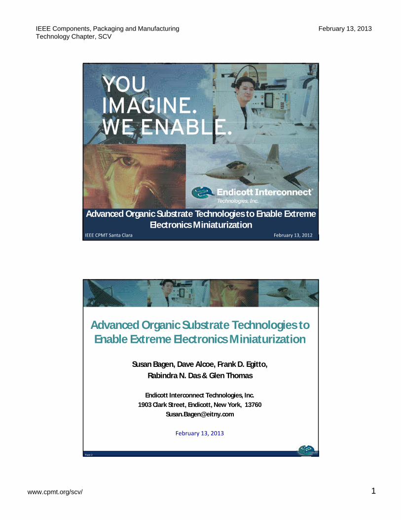
IEEE Components, Packaging and Manufacturing Technology Chapter, SCV February 13, 2013 www.cpmt.org/scv/ 1 Page 1 Advanced Organic Substrate Technologies to Enable Extreme Electronics Miniaturization IEEE CPMT Santa Clara February 13, 2012 Advanced Organic Substrate Technologies to Enable Extreme Electronics Miniaturization Enable Extreme Electronics Miniaturization Susan Bagen, Dave Alcoe, Frank D. Egitto, Rabindra N. Das & Glen Thomas Endicott Interconnect Technologies, Inc. Page 2 Endicott Interconnect Technologies, Inc. 1903 Clark Street, Endicott, New York, 13760 [email protected] February 13, 2013
Transcript of Advanced Organic Substrate Technologies to Enable … · Advanced Organic Substrate Technologies to...
IEEE Components, Packaging and Manufacturing Technology Chapter, SCV
February 13, 2013
www.cpmt.org/scv/ 1
Page 1
Advanced Organic Substrate Technologies to Enable Extreme Electronics Miniaturization
IEEE CPMT Santa Clara February 13, 2012
Advanced Organic Substrate Technologies to Enable Extreme Electronics MiniaturizationEnable Extreme Electronics Miniaturization
Susan Bagen, Dave Alcoe, Frank D. Egitto,
Rabindra N. Das & Glen Thomas
Endicott Interconnect Technologies, Inc.
Page 2
Endicott Interconnect Technologies, Inc.
1903 Clark Street, Endicott, New York, 13760
February 13, 2013
IEEE Components, Packaging and Manufacturing Technology Chapter, SCV
February 13, 2013
www.cpmt.org/scv/ 2
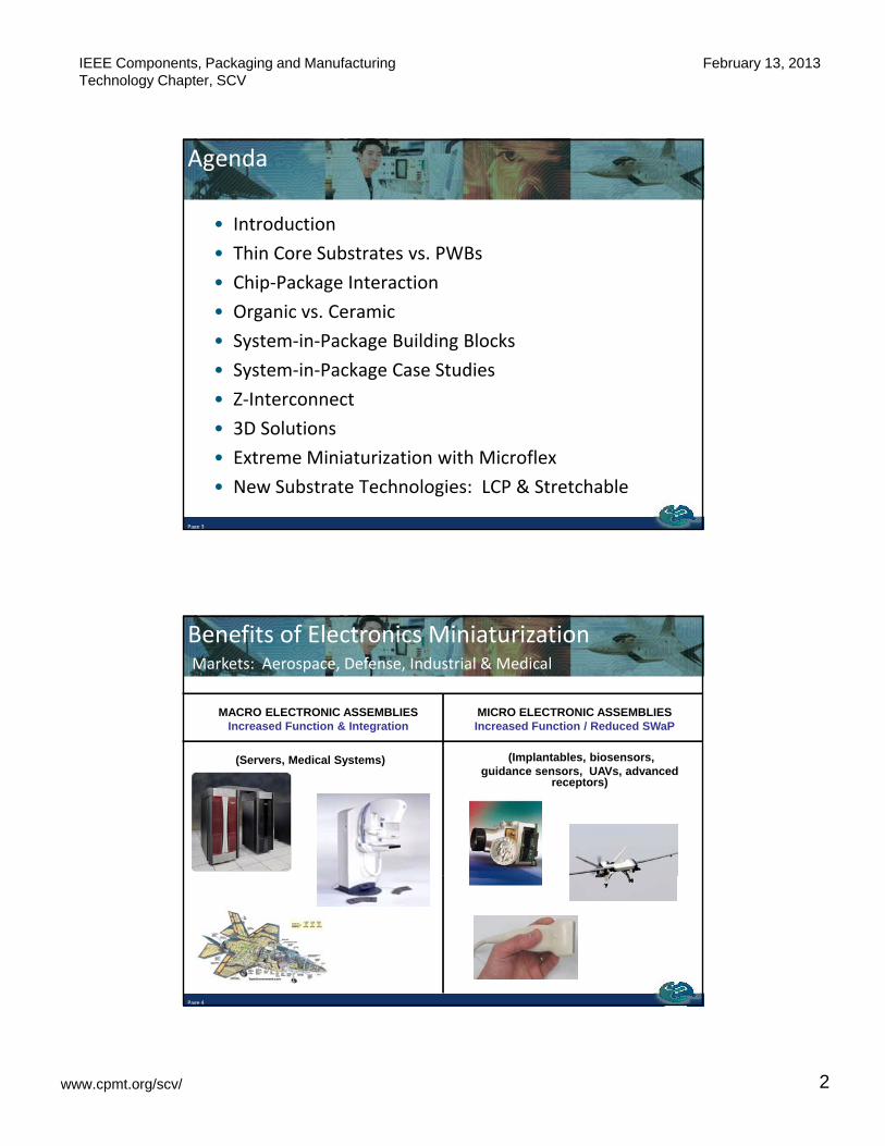
Agenda
• Introduction
• Thin Core Substrates vs. PWBs
• Chip-Package Interaction
• Organic vs. Ceramic
• System-in-Package Building Blocks
• System-in-Package Case Studies
• Z-Interconnect
Page 3
• Z-Interconnect
• 3D Solutions
• Extreme Miniaturization with Microflex
• New Substrate Technologies: LCP & Stretchable
Markets: Aerospace, Defense, Industrial & Medical
MACRO ELECTRONIC ASSEMBLIESIncreased Function & Integration
MICRO ELECTRONIC ASSEMBLIESIncreased Function / Reduced SWaP
Benefits of Electronics Miniaturization
(Servers, Medical Systems) (Implantables, biosensors, guidance sensors, UAVs, advanced
receptors)
Page 4

IEEE Components, Packaging and Manufacturing Technology Chapter, SCV
February 13, 2013
www.cpmt.org/scv/ 3
Rigid Substrates
Thin Core Substrates vs. PWBs
Page 5
Rigid Substrates
• Electronics miniaturization drives the use of fine pitch BGAs, CSPs and tiny SMT components, as well as bare die.
Substrate attributes have significant impact on the ability to reliably assemble these types of components and bare die.
• Dielectric material & filler: glass cloth vs. particle
• Substrate thickness
Page 6
• Blind & buried vias
• Line width & space capability
IEEE Components, Packaging and Manufacturing Technology Chapter, SCV
February 13, 2013
www.cpmt.org/scv/ 4
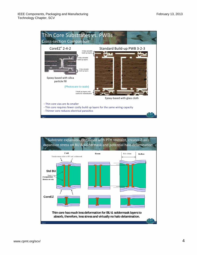
Standard Build-up PWB 3-2-3CoreEZ® 2-4-2
Thin Core Substrates vs. PWBsCross-section Comparison
2 fully wireablebuild up layers
3 fully wireablebuild up layers
(Photos are to scale)
build up layers
2 fully wireablebuild up layers
Epoxy-based with silica particle fill
Page 7
- Thin core vias are 4x smaller- Thin core requires fewer costly build up layers for the same wiring capacity- Thinner core reduces electrical parasitics
3 build up layers only useful for redistribution
Epoxy-based with glass cloth
Substrate expansion, combined with PTH restraint, creates Z-axis
expansion stress on BU & soldermask and potential halo delamination.
Std BU
Z-expansionStress on via
Page 8
CoreEZ
Thin core has much less deformation for BU & soldermask layers to absorb, therefore, less stress and virtually no halo delamination.
IEEE Components, Packaging and Manufacturing Technology Chapter, SCV
February 13, 2013
www.cpmt.org/scv/ 5
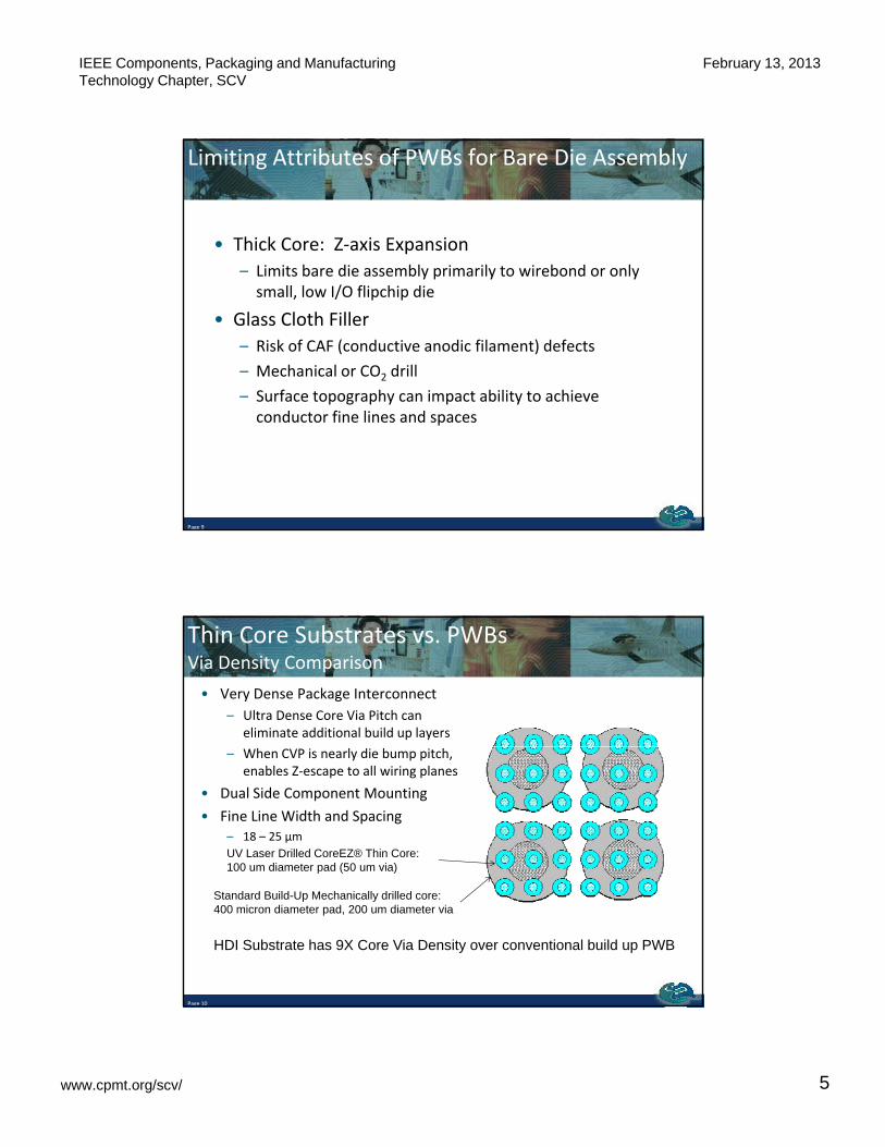
Limiting Attributes of PWBs for Bare Die Assembly
• Thick Core: Z-axis Expansion
Limits bare die assembly primarily to wirebond or only– Limits bare die assembly primarily to wirebond or only small, low I/O flipchip die
• Glass Cloth Filler
– Risk of CAF (conductive anodic filament) defects
– Mechanical or CO2 drill
– Surface topography can impact ability to achieve
Page 9
Surface topography can impact ability to achieve conductor fine lines and spaces
Thin Core Substrates vs. PWBsVia Density Comparison
• Very Dense Package Interconnect
– Ultra Dense Core Via Pitch can eliminate additional build up layers
– When CVP is nearly die bump pitch, enables Z-escape to all wiring planes
• Dual Side Component Mounting
• Fine Line Width and Spacing– 18 – 25 µm
UV Laser Drilled CoreEZ® Thin Core: 100 um diameter pad (50 um via)
Page 10
HDI Substrate has 9X Core Via Density over conventional build up PWB
Standard Build-Up Mechanically drilled core: 400 micron diameter pad, 200 um diameter via
IEEE Components, Packaging and Manufacturing Technology Chapter, SCV
February 13, 2013
www.cpmt.org/scv/ 6
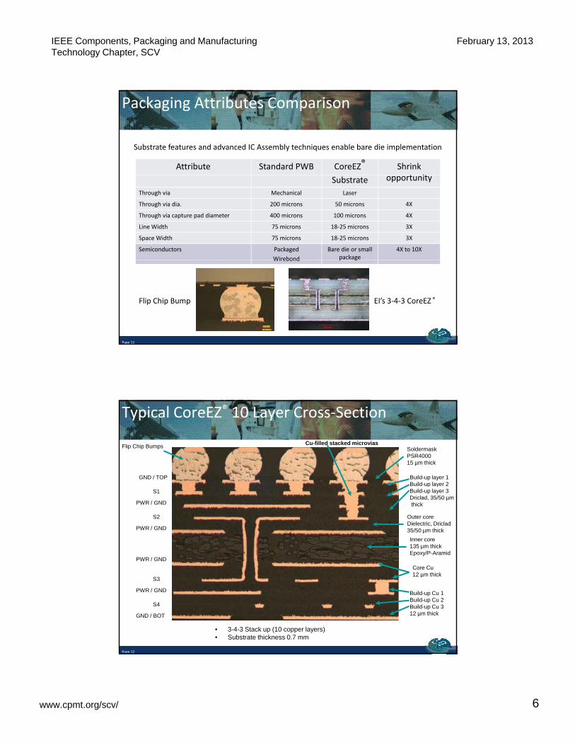
Packaging Attributes Comparison
Attribute Standard PWB CoreEZ® Shrink t it
Substrate features and advanced IC Assembly techniques enable bare die implementation
Substrate opportunity
Through via Mechanical Laser
Through via dia. 200 microns 50 microns 4X
Through via capture pad diameter 400 microns 100 microns 4X
Line Width 75 microns 18-25 microns 3X
Space Width 75 microns 18-25 microns 3X
Semiconductors Packaged
Wirebond
Bare die or small package
4X to 10X
Page 11
Wirebond p g
EI’s 3-4-3 CoreEZ ®Flip Chip Bump
Typical CoreEZ® 10 Layer Cross-Section
GND / TOP
SoldermaskPSR400015 µm thick
Build-up layer 1Build-up layer 2
Cu-filled stacked microviasFlip Chip Bumps
S1
PWR / GND
S2
PWR / GND
PWR / GND
Build-up layer 2Build-up layer 3Driclad, 35/50 µmthick
Inner core135 µm thickEpoxy/P-Aramid
Outer coreDielectric, Driclad35/50 µm thick
Core Cu
Page 12
S3
S4
PWR / GND
GND / BOT
Build-up Cu 1Build-up Cu 2Build-up Cu 312 µm thick
Core Cu12 µm thick
• 3-4-3 Stack up (10 copper layers)• Substrate thickness 0.7 mm

IEEE Components, Packaging and Manufacturing Technology Chapter, SCV
February 13, 2013
www.cpmt.org/scv/ 7
Typical HyperBGA® 9 Layer Cross Section
Non soldermask defined pad
40 micron thick KPPEouter dielectricEr = 3 2
Chip
Bump Underfill
35 micron thick PTFEDielectric, Er = 2.7
Er = 3.2 p
50 micron thick PTFEDielectric, Er = 2.7
microvia
12 thick Cu
6 Cu/38 Invar/6 CuGround plane
15 thick Cu, redistribution
Page 13
BGA Pad
15 thick Cu, redistribution
12 thick Cu, 50m dia. through via KPPE filled
Shown: 7 layer core with 1 build-up. Alternatives: Core (3-7 layer), BU to 3x layers.Can also use a traditional soldermask for SMD defined pads, if desired.
Chip-Package Interaction
Page 14

IEEE Components, Packaging and Manufacturing Technology Chapter, SCV
February 13, 2013
www.cpmt.org/scv/ 8
Flip-Chip vs. Wirebond
Wirebond: Active face is away from the substrate and associated die adhesive
Die adhesive material stress cracking avoids wirebond connections - at firstBegs questions: How far will crack run? Why did it happen? Thermal performance?
Flip-Chip: Die is 'flipped' so that electrical connections to substrate have very short length
The connections and active die face are in proximity to the substrate and underfillUnderfill is used to avoid stress to the electrical connections
Fracture / debond may not damage the wirebond
Page 15
Failure of the underfill can quickly lead to electrical opens
Thermal expansion of the Die vs Substrate is one fundamental driver of reliability
Fracture / debond likely to damage the bump
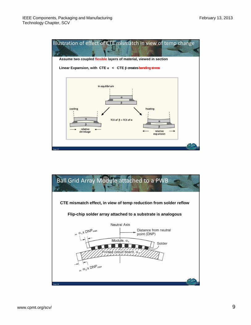
Illustration of effect of CTE mismatch in view of temp change
Assume two very stiff layers of material, viewed in section
Linear Expansion Only, with CTE α < CTE β
α
β
αα
Equilibrium Temperature
HeatedCooled
Page 16
ββ
With temperature change, dissimilar materials expand differently: “Mismatch”This expansion mismatch creates strain and stressThe strain and stress exists in either the materials, the bonding , or both
IEEE Components, Packaging and Manufacturing Technology Chapter, SCV
February 13, 2013
www.cpmt.org/scv/ 9
Illustration of effect of CTE mismatch in view of temp change
Assume two coupled flexible layers of material, viewed in section
Linear Expansion, with CTE α < CTE β creates bending stress
Page 17
Ball Grid Array Module attached to a PWB
CTE mismatch effect, in view of temp reduction from solder reflow
Flip-chip solder array attached to a substrate is analogous
Page 18
IEEE Components, Packaging and Manufacturing Technology Chapter, SCV
February 13, 2013
www.cpmt.org/scv/ 10
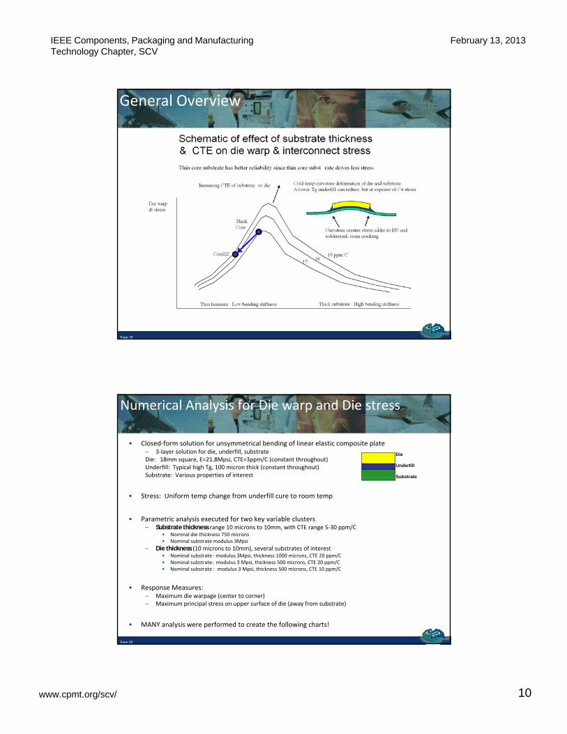
General Overview
Page 19
Numerical Analysis for Die warp and Die stress
• Closed-form solution for unsymmetrical bending of linear elastic composite plate– 3-layer solution for die, underfill, substrateDie: 18mm square, E=21.8Mpsi, CTE=3ppm/C (constant throughout)Underfill: Typical high Tg, 100 micron thick (constant throughout)Substrate: Various properties of interest
Die
Underfill
Substratep p
• Stress: Uniform temp change from underfill cure to room temp
• Parametric analysis executed for two key variable clusters– Substrate thickness range 10 microns to 10mm, with CTE range 5-30 ppm/C
• Nominal die thickness 750 microns• Nominal substrate modulus 3Mpsi
– Die thickness (10 microns to 10mm), several substrates of interest• Nominal substrate : modulus 3Mpsi, thickness 1000 microns, CTE 20 ppm/C
N i l b t t d l 3 M i thi k 500 i CTE 20 /C
Substrate
Page 20
• Nominal substrate: modulus 3 Mpsi, thickness 500 microns, CTE 20 ppm/C• Nominal substrate : modulus 3 Mpsi, thickness 500 microns, CTE 10 ppm/C
• Response Measures: – Maximum die warpage (center to corner) – Maximum principal stress on upper surface of die (away from substrate)
• MANY analysis were performed to create the following charts!

IEEE Components, Packaging and Manufacturing Technology Chapter, SCV
February 13, 2013
www.cpmt.org/scv/ 11
• CTE difference from silicon is key driver
• Substrate thickness creates a significant
Substrate Thickness & CTE EffectsComparison for common die size
15
20
25
30
Die STRESS
5 ppm/C
30
gmaximum response value for both die stress and die warpage
• For substrates above the maximal response value, thinning the substrate is worse
• For substrates below the maximal response value, thinning the substrate is
Page 21
5 ppm/C
10Die WARP
Typical flip-chip pkg rangePWB rangeWafer-level pkg
gbetter
• Nominal substrate modulus 3 Mpsi
• To compare actual designs, their stiffness will vary, along with thickness & CTE
HyperBGA
20 ppm/C, 1000micron20 ppm/C, 500micron
Die Thickness EffectComparison for three nominal substrates
• Strong effect of silicon thickness on warpage
• Silicon must become extremely thin to underpass maximum so Die STRESS
20 ppm/C, 500micron
20 ppm/C, 1000micron
10 ppm/C, 500micron
underpass maximum, so that most substrate application will warp MORE with thinner die
• Substrate properties have significant effect on die warpage
• Starting from typical die thickness, stress generally drops as die is thinned, but eventually
h i t h it
Page 22
Die WARP
10 ppm/C, 500micron
TypicalASIC
Typical thinned
Stacked (unthinned)
reaches point where it becomes compressed
• Thinned stacked die has potential to create layer-layer debonding stress, depending on substrate choice (similar to ULK ILD issues)
IEEE Components, Packaging and Manufacturing Technology Chapter, SCV
February 13, 2013
www.cpmt.org/scv/ 12
Organic vs. Ceramic Substrates
Page 23
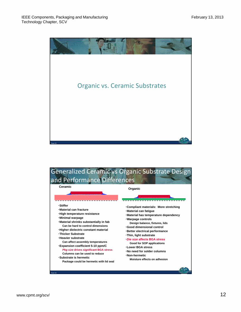
Generalized Ceramic vs Organic Substrate Design and Performance Differences
CeramicOrganic
StifferMaterial can fractureHigh temperature resistance Minimal warpageMaterial shrinks substantially in fab
Can be hard to control dimensions
Higher dielectric constant materialThicker SubstrateHeavier substrate
Compliant materials: More stretchingMaterial can fatigue Material has temperature dependencyWarpage controls
Design balance, fixtures, lids
Good dimensional controlBetter electrical performanceThin, light substrateDi i ff t BGA t
Page 24
Heavier substrateCan affect assembly temperatures
Expansion coefficient 5-10 ppm/CPkg size drives significant BGA stressColumns can be used to reduce
Substrate is hermeticPackage could be hermetic with lid seal
Die size affects BGA stressGood for SOP applications
Lower BGA stressNo need for solder columnsNon-hermetic
Moisture effects on adhesion
IEEE Components, Packaging and Manufacturing Technology Chapter, SCV
February 13, 2013
www.cpmt.org/scv/ 13
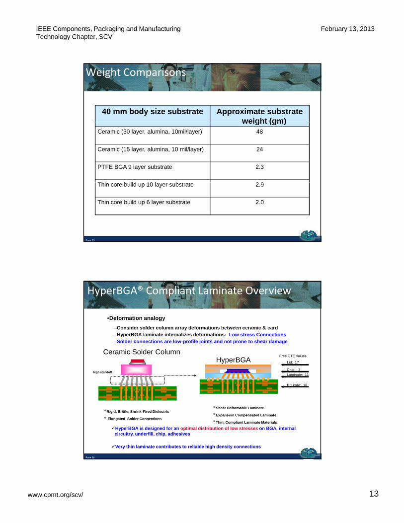
Weight Comparisons
40 mm body size substrate Approximate substrate weight (gm)weight (gm)
Ceramic (30 layer, alumina, 10mil/layer) 48
Ceramic (15 layer, alumina, 10 mil/layer) 24
PTFE BGA 9 layer substrate 2.3
Thi b ild 10 l b t t 2 9
Page 25
Thin core build up 10 layer substrate 2.9
Thin core build up 6 layer substrate 2.0
Deformation analogy
–Consider solder column array deformations between ceramic & card–HyperBGA laminate internalizes deformations: Low stress Connections
S ld ti l fil j i t d t t h d
HyperBGA® Compliant Laminate Overview
Ceramic Solder ColumnHyperBGA Lid: 17
Chip: 3Laminate: 11
PC card: 18
Free CTE values
–Solder connections are low-profile joints and not prone to shear damage
high standoff
Page 26
HyperBGA is designed for an optimal distribution of low stresses on BGA, internal circuitry, underfill, chip, adhesives
Very thin laminate contributes to reliable high density connections
Shear Deformable Laminate
Expansion Compensated Laminate
Thin, Compliant Laminate Materials
Rigid, Brittle, Shrink-Fired Dielectric
Elongated Solder Connections

IEEE Components, Packaging and Manufacturing Technology Chapter, SCV
February 13, 2013
www.cpmt.org/scv/ 14
Ceramic Solder Columndeformations in solder
SCM HyperBGAdeformations internalized
HyperBGA® Compliant Laminate Overview
MCM HyperBGA
high standoff low standoff
Page 27
PWB
Laminate
Lid
ypdeformations internalized and localized
Localized Deformation is ideal for multi-component reliability
–Thin-film behavior of thin laminate: Very little interaction between components–Low stress interconnections exist for each subcomponent
–Non-underfilled CSP and passives are successful
Compliant Laminate Advantage
–PWB Connections remain low-profile and not prone to shear damage
The Lid combines roles of heatspreading and overall flatness control
–Pre-attached laminate 'stiffener' is unnecessary, even with 0.5mm thick laminate–Use of thick aluminum lid provides extreme flatness and excellent PWB match
–ALSIC material unnecessary so far –Compliant adhesives provide outstanding thermal and mechanical support
Laminate
Lid
Page 28
MCM organic package size can be irrelevant to board level reliabilty through optimal design and construction.
PWB
Laminate

IEEE Components, Packaging and Manufacturing Technology Chapter, SCV
February 13, 2013
www.cpmt.org/scv/ 15
System-in-Package (SiP) Building Blocks
Page 29
Standard Build up 3 2 3CoreEZ® 2 4 2
Building BlocksSiP Fabrication & Assembly Technology
• Substrate Technology– Replace bulky, thick PWBs with thin, high density substrates
Standard Build-up 3-2-3CoreEZ® 2-4-2
Page 30
Photos are same magnification.Vias are 4X smaller.Core via pitch matches die.Short via length for low Z-expansion stress.
IEEE Components, Packaging and Manufacturing Technology Chapter, SCV
February 13, 2013
www.cpmt.org/scv/ 16
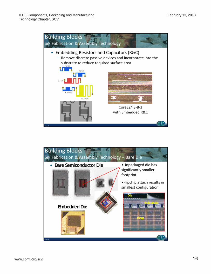
• Embedding Resistors and Capacitors (R&C)– Remove discrete passive devices and incorporate into the
substrate to reduce required surface area
Building BlocksSiP Fabrication & Assembly Technology
q
Page 31
CoreEZ® 3-8-3with Embedded R&C
• Bare Semiconductor Die
Building BlocksSiP Fabrication & Assembly Technology – Bare Die
•Unpackaged die has significantly smaller footprint.
•Flipchip attach results in smallest configuration.
Substrate
Die
Embedded Die
Page 32
PWB
IEEE Components, Packaging and Manufacturing Technology Chapter, SCV
February 13, 2013
www.cpmt.org/scv/ 17
System-in-Package (SiP)Application Examples
Page 33
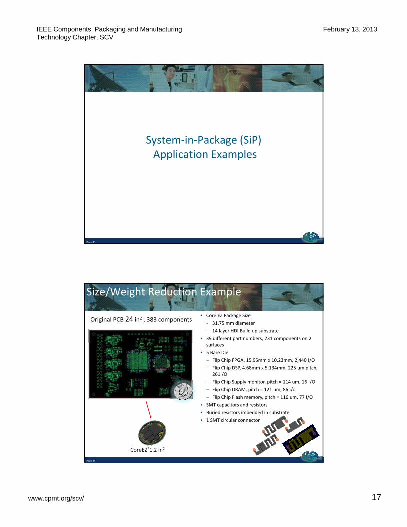
• Core EZ Package Size
- 31.75 mm diameter
- 14 layer HDI Build up substrate
• 39 different part numbers, 231 components on 2
Original PCB 24 in2 , 383 components
Size/Weight Reduction Example
surfaces
• 5 Bare Die
– Flip Chip FPGA, 15.95mm x 10.23mm, 2,440 I/O
– Flip Chip DSP, 4.68mm x 5.134mm, 225 um pitch, 261I/O
– Flip Chip Supply monitor, pitch = 114 um, 16 I/O
– Flip Chip DRAM, pitch = 121 um, 86 i/o
– Flip Chip Flash memory, pitch = 116 um, 77 I/O
Page 34
• SMT capacitors and resistors
• Buried resistors imbedded in substrate
• 1 SMT circular connector
CoreEZ®1.2 in2
IEEE Components, Packaging and Manufacturing Technology Chapter, SCV
February 13, 2013
www.cpmt.org/scv/ 18
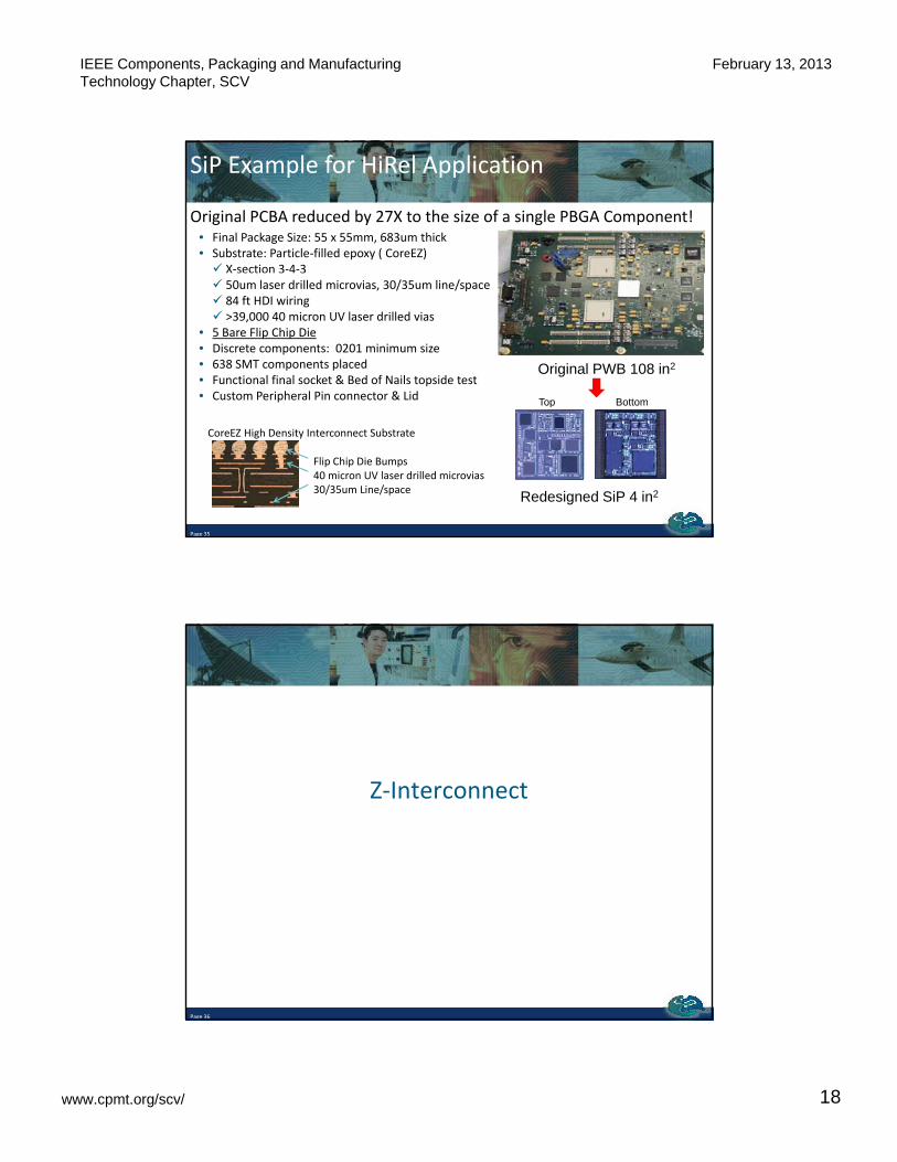
• Final Package Size: 55 x 55mm, 683um thick• Substrate: Particle-filled epoxy ( CoreEZ) X-section 3-4-3
SiP Example for HiRel Application
Original PCBA reduced by 27X to the size of a single PBGA Component!
50um laser drilled microvias, 30/35um line/space 84 ft HDI wiring >39,000 40 micron UV laser drilled vias
• 5 Bare Flip Chip Die• Discrete components: 0201 minimum size• 638 SMT components placed • Functional final socket & Bed of Nails topside test• Custom Peripheral Pin connector & Lid
Original PWB 108 in2
Top Bottom
Page 35
CoreEZ High Density Interconnect Substrate
Flip Chip Die Bumps40 micron UV laser drilled microvias30/35um Line/space
Redesigned SiP 4 in2
Top Bottom
Z-Interconnect
Page 36
IEEE Components, Packaging and Manufacturing Technology Chapter, SCV
February 13, 2013
www.cpmt.org/scv/ 19
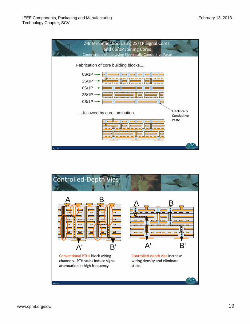
Fabrication of core building blocks.....
0S/1P
Z-Interconnection Using 2S/1P Signal Cores and 0S/1P Joining Cores
Connections Made Using Electrically Conductive Paste
0S/1P
0S/1P
2S/1P
2S/1P
followed by core lamination Electrically
Page 37
.....followed by core lamination.Conductive Paste
A B A B
Controlled-Depth Vias
A' B' A' B'
Page 38
A B A BConventional PTHs block wiring channels. PTH stubs induce signal attenuation at high frequency.
Controlled-depth vias increase wiring density and eliminate stubs.
IEEE Components, Packaging and Manufacturing Technology Chapter, SCV
February 13, 2013
www.cpmt.org/scv/ 20
100%
Parallel vs. Sequential Process Yields
Why Z-Interconnect?
20%
40%
60%
80%
100%O
vera
ll Y
ield
2 Layer Sequential
8 Layer Sequential
2 Layer Parallel
Page 39
60%70%80%90%100%
Individual Layer Yield
0%
8 Layer Parallel
Assumes Layer Joining Yield = 1 - 0.25 x (1 - Layer Yield)
Nanotechnology : A Complete SolutionEndicott Interconnect Proprietary and Confidential
Nano Materials formulation
Joining core
Assembly
Performance
Z-Interconnects
Page 40
Sintering
Hyper-ZFull-Z Rigid-flex
Board-Z
IEEE Components, Packaging and Manufacturing Technology Chapter, SCV
February 13, 2013
www.cpmt.org/scv/ 21
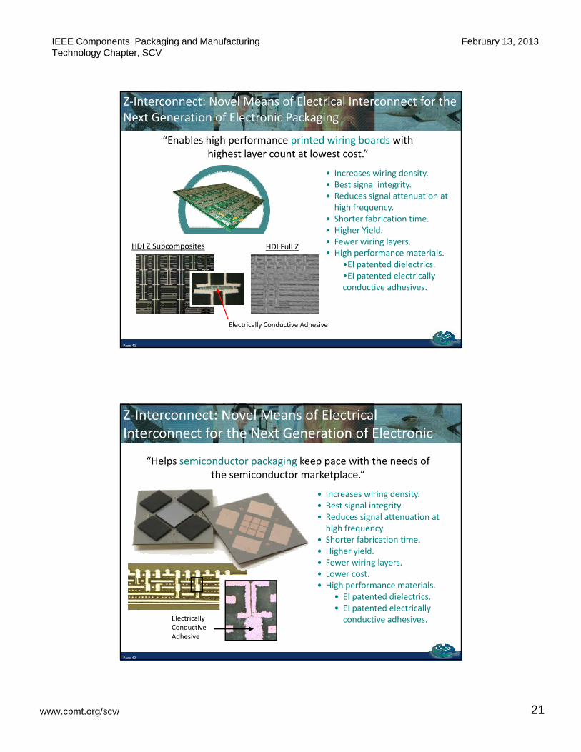
• Increases wiring density.
“Enables high performance printed wiring boards with highest layer count at lowest cost.”
Z-Interconnect: Novel Means of Electrical Interconnect for the Next Generation of Electronic Packaging
g y• Best signal integrity.• Reduces signal attenuation at
high frequency.• Shorter fabrication time.• Higher Yield.• Fewer wiring layers.• High performance materials.
EI t t d di l t i
HDI Full ZHDI Z Subcomposites
Page 41
•EI patented dielectrics.•EI patented electrically conductive adhesives.
Electrically Conductive Adhesive
Z-Interconnect: Novel Means of Electrical Interconnect for the Next Generation of Electronic Packaging
“Helps semiconductor packaging keep pace with the needs of the semiconductor marketplace.”
• Increases wiring density.• Best signal integrity.• Reduces signal attenuation at
high frequency.• Shorter fabrication time.• Higher yield.• Fewer wiring layers.• Lower cost
Page 42
• Lower cost.• High performance materials.
• EI patented dielectrics.• EI patented electrically
conductive adhesives.Electrically Conductive Adhesive
IEEE Components, Packaging and Manufacturing Technology Chapter, SCV
February 13, 2013
www.cpmt.org/scv/ 22
RigidRigid--FlexFlex
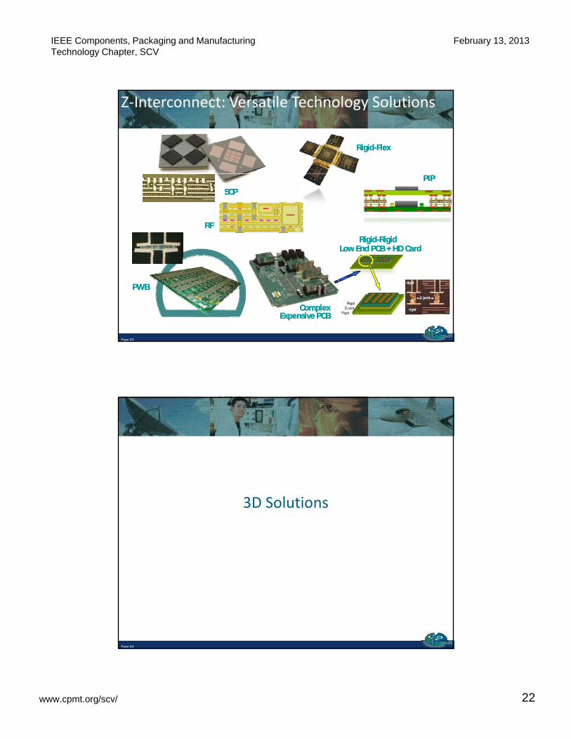
Z-Interconnect: Versatile Technology Solutions
PIP PIP
RFRF
RigidRigid--RigidRigid
SCPSCP
Low End PCB + HD CardLow End PCB + HD Card
Page 43
PWBPWB
Complex Complex Expensive PCBExpensive PCB
3D Solutions
Page 44

IEEE Components, Packaging and Manufacturing Technology Chapter, SCV
February 13, 2013
www.cpmt.org/scv/ 23
3D PackagingPackage-Interposer-Package (PIP) Technology
A new 3D “Package Interposer Package” (PIP) solution is suitable for combining multiple memory, ASICs, stacked die, stacked packaged die,
etc., into a single package.
Page 45
Schematic of Package-Interposer-Package (PIP) construction with 4 packages and 3 interposers
3D PackagingPackage-Interposer-Package (PIP) Technology
Benefits of Package-Interposer-Package
• High density, small pitch
• Re-workable and replaceable• Re-workable and replaceable
• Polymer or ceramic interposer provides additional support for improving stability and reliability
• PIP will experience less warpage and thermal stress
• Mitigates problems with coplanarity between
packages
Page 46
• Interposer Options:– Dielectric material
– Embedded passives
– Embedded actives

IEEE Components, Packaging and Manufacturing Technology Chapter, SCV
February 13, 2013
www.cpmt.org/scv/ 24
Package-Interposer-Package vs. POP
Page 47
PIP increases density while not adding to overall package thickness.
3D Multiple Interposers
Example: 4 assembled packages connected with 3
Page 48
Example: 4 assembled packages connected with 3 interposers.-Simpler assembled packages readily integrated into resulting complex, high density 3D structure-Versatility of construction-Can be removed, repaired, upgraded
IEEE Components, Packaging and Manufacturing Technology Chapter, SCV
February 13, 2013
www.cpmt.org/scv/ 25
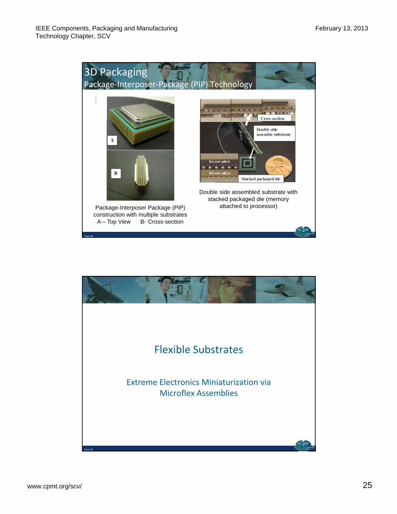
3D PackagingPackage-Interposer-Package (PIP) Technology
Page 49
Package-Interposer Package (PiP) construction with multiple substrates
A – Top View B- Cross-section
Double side assembled substrate with stacked packaged die (memory
attached to processor)
Flexible Substrates
Extreme Electronics Miniaturization via Microflex Assemblies
Page 50
Microflex Assemblies

IEEE Components, Packaging and Manufacturing Technology Chapter, SCV
February 13, 2013
www.cpmt.org/scv/ 26
Microflex Device Packaging
Die & Other Components
• ASIC Die
• PZT PLZT PMN PT• PZT, PLZT, PMN-PT
• SMT Passives
Substrate Fabrication
• 12.5 µm thick polyimide
• 25 μm laser drilled vias (minimum)
• 11/11μm line width & space (minimum)
C bl
Page 51
IC Assembly
• Flip chip pitch down to 70 μm (minimum)
Module Tester
• Full functional module test
Micro Pillar Technology for Finer Pitch Applications
Page 52
ASIC die with 70 µm bonding pad pitch, 22 µm diameter pillar
IEEE Components, Packaging and Manufacturing Technology Chapter, SCV
February 13, 2013
www.cpmt.org/scv/ 27
Microflex Assembly PackageExtreme Miniaturization
• Sensor assembly rolled to 1.175mm diameter
Single layer HDI Flex
Flip Chip Bumps
• 5 Flip Chip ASIC,.1mm thick, 31 I/O each, 2.5mm x 0.5mm
– 22 micron flip chip bumps on 70 micron die pad pitch
• 12.5mm by 6.5 mm single layer flex circuit
– 14 micron wide lines and space copper circuitry
12 5 i hi k l i id di l i
200 µm
ASIC Die
Page 53
– 12.5 micron thick polyimide dielectric
• Prototype to production
– Over 1.5M shipped
11 li /
High Density Double-Sided Flex
• 11 µm lines / spaces
• 25 µm vias
• 6 µm thick metallurgy
• 12.5 µm polyimide
• Flexible soldermask
FC ASIC Di & SMT i
Page 54
• FC ASIC Die & SMT passives
ASIC Die 12x6 mm, 200 µm thick

IEEE Components, Packaging and Manufacturing Technology Chapter, SCV
February 13, 2013
www.cpmt.org/scv/ 28
Multilayer Flex – Study to Define Design Rules
Flex
Flex
Bond-ply
Page 55
1. Cu Thickness
2. Flex thickness
3. Bond-ply thickness
Roll
Bend/Flex
Flex
Degree of Flexibility
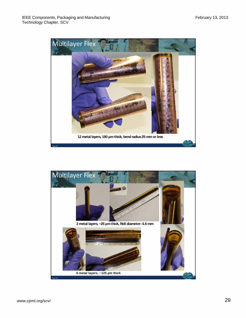
Multilayer Flex
Page 56
12 metal layers, 325 – 330 µm thick, bend radius 25 mm or higher
IEEE Components, Packaging and Manufacturing Technology Chapter, SCV
February 13, 2013
www.cpmt.org/scv/ 29
Multilayer Flex
Page 57
12 metal layers, 190 µm thick, bend radius 25 mm or less
Multilayer Flex
2 metal layers, ~25 µm thick, Roll diameter: 4.6 mm
Page 58
6 metal layers, ~125 µm thick
IEEE Components, Packaging and Manufacturing Technology Chapter, SCV
February 13, 2013
www.cpmt.org/scv/ 30
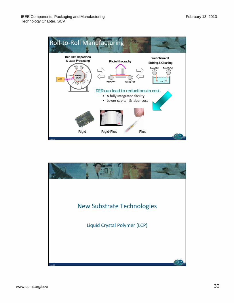
Roll-to-Roll Manufacturing
Thin Film Deposition& Laser Processing Photolithography
Supply Roll Take-Up Roll
Wet Chemical
Etching & Cleaning
Supply Roll Take-Up Roll
CoolingDrum
Laser
R2R can lead to reductions in cost.• A fully integrated facility• Lower capital & labor cost
Page 59
Azores PhotolithographyFlexRigid-FlexRigid
New Substrate Technologies
Liquid Crystal Polymer (LCP)
Page 60
IEEE Components, Packaging and Manufacturing Technology Chapter, SCV
February 13, 2013
www.cpmt.org/scv/ 31
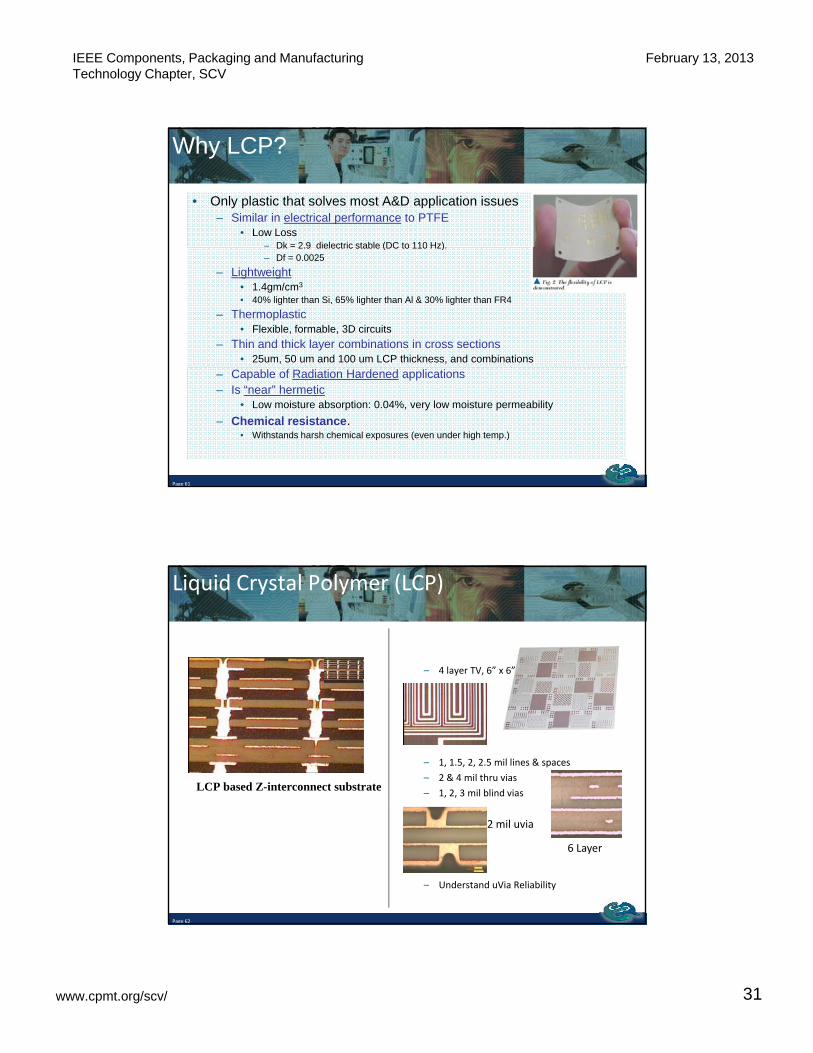
• Only plastic that solves most A&D application issues– Similar in electrical performance to PTFE
• Low Loss– Dk = 2.9 dielectric stable (DC to 110 Hz).
Why LCP?
Dk 2.9 dielectric stable (DC to 110 Hz).– Df = 0.0025
– Lightweight• 1.4gm/cm3
• 40% lighter than Si, 65% lighter than Al & 30% lighter than FR4
– Thermoplastic• Flexible, formable, 3D circuits
– Thin and thick layer combinations in cross sections• 25um, 50 um and 100 um LCP thickness, and combinations
Page 61
– Capable of Radiation Hardened applications– Is “near” hermetic
• Low moisture absorption: 0.04%, very low moisture permeability
– Chemical resistance. • Withstands harsh chemical exposures (even under high temp.)
Liquid Crystal Polymer (LCP)
– 4 layer TV, 6” x 6”
LCP based Z-interconnect substrate
– 1, 1.5, 2, 2.5 mil lines & spaces
– 2 & 4 mil thru vias
– 1, 2, 3 mil blind vias
Page 62
– Understand uVia Reliability
6 Layer
2 mil uvia

IEEE Components, Packaging and Manufacturing Technology Chapter, SCV
February 13, 2013
www.cpmt.org/scv/ 32
LCP based Rigid-Flex
Page 63
Rigid Flex gives the ability to design circuitry to fit the device, rather than building the device to fit the circuitry.
Stretchable Substrates
Conformable Electronics
Page 64
IEEE Components, Packaging and Manufacturing Technology Chapter, SCV
February 13, 2013
www.cpmt.org/scv/ 33
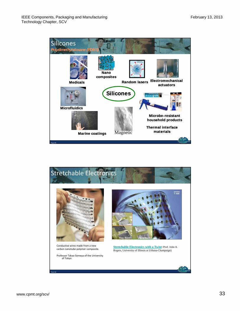
SiliconesPolydimethylsiloxane (PDMS)
Si O
CH3
CH3n
NanoNano
SiliconesSilicones
Nano Nano compositescomposites
MicrofluidicsMicrofluidics
MedicalsMedicals ElectromechanicalElectromechanicalactuatorsactuators
Random lasersRandom lasers
Page 65
Marine coatingsMarine coatings
MicrofluidicsMicrofluidics
MicrobeMicrobe--resistantresistanthousehold productshousehold products
Thermal interface Thermal interface materialsmaterialsMagnetic
Stretchable Electronics
Page 66
Conductive wires made from a new carbon nanotube-polymer composite.
Professor Takao Someya of the University of Tokyo
Stretchable Electronics with a Twist: Prof. John A. Rogers, University of Illinois at Urbana-Champaign)
IEEE Components, Packaging and Manufacturing Technology Chapter, SCV
February 13, 2013
www.cpmt.org/scv/ 34
Stretchable ElectronicsProcess Development for Metal Adhesion
• Bio-compatible
• Bio-stable
Fi li• Fine lines
silicone
SiOx
Page 67
Metal
Water Soluble PVA Substrate
Page 68

IEEE Components, Packaging and Manufacturing Technology Chapter, SCV
February 13, 2013
www.cpmt.org/scv/ 35
Summary
Advanced Electronics Packaging for A&D, industrial and medical applications is driving the need for novelmedical applications is driving the need for novel
substrate materials, ultra high density assemblies and unique form factors.
Substrate materials and construction are key to overall package performance and reliability.
Page 69
Thank you for your attention!